KR20120099341A - Semiconductor device and manufacturing method thereof - Google Patents
Semiconductor device and manufacturing method thereof Download PDFInfo
- Publication number
- KR20120099341A KR20120099341A KR1020120007150A KR20120007150A KR20120099341A KR 20120099341 A KR20120099341 A KR 20120099341A KR 1020120007150 A KR1020120007150 A KR 1020120007150A KR 20120007150 A KR20120007150 A KR 20120007150A KR 20120099341 A KR20120099341 A KR 20120099341A
- Authority
- KR
- South Korea
- Prior art keywords
- oxide semiconductor
- insulating film
- film
- semiconductor film
- transistor
- Prior art date
- Legal status (The legal status is an assumption and is not a legal conclusion. Google has not performed a legal analysis and makes no representation as to the accuracy of the status listed.)
- Granted
Links
Images


Classifications
-
- H—ELECTRICITY
- H10—SEMICONDUCTOR DEVICES; ELECTRIC SOLID-STATE DEVICES NOT OTHERWISE PROVIDED FOR
- H10D—INORGANIC ELECTRIC SEMICONDUCTOR DEVICES
- H10D30/00—Field-effect transistors [FET]
- H10D30/60—Insulated-gate field-effect transistors [IGFET]
- H10D30/67—Thin-film transistors [TFT]
- H10D30/6704—Thin-film transistors [TFT] having supplementary regions or layers in the thin films or in the insulated bulk substrates for controlling properties of the device
-
- H—ELECTRICITY
- H10—SEMICONDUCTOR DEVICES; ELECTRIC SOLID-STATE DEVICES NOT OTHERWISE PROVIDED FOR
- H10D—INORGANIC ELECTRIC SEMICONDUCTOR DEVICES
- H10D30/00—Field-effect transistors [FET]
- H10D30/01—Manufacture or treatment
- H10D30/021—Manufacture or treatment of FETs having insulated gates [IGFET]
- H10D30/031—Manufacture or treatment of FETs having insulated gates [IGFET] of thin-film transistors [TFT]
-
- H—ELECTRICITY
- H10—SEMICONDUCTOR DEVICES; ELECTRIC SOLID-STATE DEVICES NOT OTHERWISE PROVIDED FOR
- H10D—INORGANIC ELECTRIC SEMICONDUCTOR DEVICES
- H10D30/00—Field-effect transistors [FET]
- H10D30/60—Insulated-gate field-effect transistors [IGFET]
- H10D30/67—Thin-film transistors [TFT]
- H10D30/6704—Thin-film transistors [TFT] having supplementary regions or layers in the thin films or in the insulated bulk substrates for controlling properties of the device
- H10D30/6713—Thin-film transistors [TFT] having supplementary regions or layers in the thin films or in the insulated bulk substrates for controlling properties of the device characterised by the properties of the source or drain regions, e.g. compositions or sectional shapes
- H10D30/6715—Thin-film transistors [TFT] having supplementary regions or layers in the thin films or in the insulated bulk substrates for controlling properties of the device characterised by the properties of the source or drain regions, e.g. compositions or sectional shapes characterised by the doping profiles, e.g. having lightly-doped source or drain extensions
-
- H—ELECTRICITY
- H10—SEMICONDUCTOR DEVICES; ELECTRIC SOLID-STATE DEVICES NOT OTHERWISE PROVIDED FOR
- H10D—INORGANIC ELECTRIC SEMICONDUCTOR DEVICES
- H10D30/00—Field-effect transistors [FET]
- H10D30/60—Insulated-gate field-effect transistors [IGFET]
- H10D30/67—Thin-film transistors [TFT]
- H10D30/674—Thin-film transistors [TFT] characterised by the active materials
- H10D30/6755—Oxide semiconductors, e.g. zinc oxide, copper aluminium oxide or cadmium stannate
-
- H—ELECTRICITY
- H10—SEMICONDUCTOR DEVICES; ELECTRIC SOLID-STATE DEVICES NOT OTHERWISE PROVIDED FOR
- H10D—INORGANIC ELECTRIC SEMICONDUCTOR DEVICES
- H10D62/00—Semiconductor bodies, or regions thereof, of devices having potential barriers
- H10D62/60—Impurity distributions or concentrations
-
- H—ELECTRICITY
- H10—SEMICONDUCTOR DEVICES; ELECTRIC SOLID-STATE DEVICES NOT OTHERWISE PROVIDED FOR
- H10D—INORGANIC ELECTRIC SEMICONDUCTOR DEVICES
- H10D99/00—Subject matter not provided for in other groups of this subclass
-
- H10W42/00—
-
- H—ELECTRICITY
- H10—SEMICONDUCTOR DEVICES; ELECTRIC SOLID-STATE DEVICES NOT OTHERWISE PROVIDED FOR
- H10D—INORGANIC ELECTRIC SEMICONDUCTOR DEVICES
- H10D30/00—Field-effect transistors [FET]
- H10D30/01—Manufacture or treatment
- H10D30/021—Manufacture or treatment of FETs having insulated gates [IGFET]
- H10D30/031—Manufacture or treatment of FETs having insulated gates [IGFET] of thin-film transistors [TFT]
- H10D30/0312—Manufacture or treatment of FETs having insulated gates [IGFET] of thin-film transistors [TFT] characterised by the gate electrodes
Landscapes
- Thin Film Transistor (AREA)
- Semiconductor Memories (AREA)
- Solid State Image Pick-Up Elements (AREA)
- Electrodes Of Semiconductors (AREA)
- Non-Volatile Memory (AREA)
- Physics & Mathematics (AREA)
- Condensed Matter Physics & Semiconductors (AREA)
- General Physics & Mathematics (AREA)
- Engineering & Computer Science (AREA)
- Computer Hardware Design (AREA)
- Microelectronics & Electronic Packaging (AREA)
- Power Engineering (AREA)
Abstract
Description
산화물 반도체를 사용하는 반도체 장치 및 상기 반도체 장치의 제조 방법에 관한 것이다.A semiconductor device using an oxide semiconductor and a method for manufacturing the semiconductor device.
또한, 본 명세서에 있어서 반도체 장치란 반도체 특성을 이용함으로써 기능할 수 있는 장치 전반을 가리킨다. 본 명세서에서의 트랜지스터는 반도체 장치이며, 상기 트랜지스터를 포함하는 표시 장치, 반도체 회로 및 전자 기기는 모두 반도체 장치에 포함된다.In addition, in this specification, a semiconductor device refers to the general apparatus which can function by using a semiconductor characteristic. The transistor in the present specification is a semiconductor device, and a display device, a semiconductor circuit, and an electronic device including the transistor are all included in the semiconductor device.
액정 표시 장치나 발광 표시 장치로 대표되는 플랫 패널 디스플레이의 대부분에 사용되고 있는 트랜지스터는 유리 기판 위에 형성된 아몰퍼스 실리콘, 단결정 실리콘 또는 다결정 실리콘 등의 실리콘 반도체에 의해 구성되어 있다. 또한, 상기 실리콘 반도체를 사용한 트랜지스터는 집적 회로(IC) 등에도 이용되고 있다.Transistors used in most of flat panel displays such as liquid crystal display devices and light emitting display devices are composed of silicon semiconductors such as amorphous silicon, single crystal silicon, or polycrystalline silicon formed on a glass substrate. The transistor using the silicon semiconductor is also used for an integrated circuit (IC) or the like.
상기 실리콘 반도체를 대신하여 반도체 특성을 나타내는 금속 산화물을 트랜지스터에 사용하는 기술이 주목받고 있다. 또한, 본 명세서에서는 반도체 특성을 나타내는 금속 산화물을 산화물 반도체라고 부르기로 한다.The technique of using the metal oxide which shows semiconductor characteristics in a transistor instead of the said silicon semiconductor is attracting attention. In addition, in this specification, the metal oxide which shows semiconductor characteristics is called an oxide semiconductor.
예를 들어, 산화물 반도체로서 산화아연, In-Ga-Zn계 금속 산화물을 사용하여 트랜지스터를 제조하고, 상기 트랜지스터를 표시 장치의 화소의 스위칭 소자 등에 사용하는 기술이 개시되어 있다(특허문헌 1 및 특허문헌 2 참조).For example, a technique is disclosed in which a transistor is manufactured using zinc oxide and an In—Ga—Zn-based metal oxide as an oxide semiconductor, and the transistor is used for a switching element of a pixel of a display device or the like (
산화물 반도체에 있어서, 산화물 반도체에 포함되는 수소가 캐리어의 공급원이 되는 것이 지적되어 있다. 그 때문에, 산화물 반도체의 형성 시에 수소가 혼입되지 않는 조치를 강구할 것이 요구된다. 또한, 산화물 반도체 뿐만 아니라, 산화물 반도체를 사용한 트랜지스터에 있어서, 산화물 반도체에 접하는 게이트 절연막의 수소를 저감함으로써 임계값 전압의 변동을 저감하고 있다(특허문헌 3 참조).In an oxide semiconductor, it is pointed out that hydrogen contained in an oxide semiconductor becomes a supply source of a carrier. Therefore, it is required to take measures to prevent hydrogen from mixing during the formation of the oxide semiconductor. In addition to the oxide semiconductor, in the transistor using the oxide semiconductor, the variation of the threshold voltage is reduced by reducing the hydrogen in the gate insulating film in contact with the oxide semiconductor (see Patent Document 3).
또한, 산화물 반도체에 있어서, 캐리어의 공급원은 산화물 반도체에 포함되는 수소의 이외에 산화물 반도체 내의 산소 결손을 들 수 있다. 상기 산소 결손의 일부는 도너가 되어, 상기 산화물 반도체 내에 캐리어인 전자를 생성한다. 따라서, 산화물 반도체를 사용한 반도체 장치에 있어서, 채널 형성 영역을 포함하는 산화물 반도체 내의 산소 결손은 상기 산화물 반도체 내에 전자를 생성시키기 위하여 상기 반도체 장치의 임계값 전압을 마이너스 방향으로 변동시키는 요인이라고 할 수 있다.In addition, in the oxide semiconductor, a source of carrier includes oxygen deficiency in the oxide semiconductor in addition to hydrogen contained in the oxide semiconductor. Part of the oxygen vacancies becomes a donor, producing electrons which are carriers in the oxide semiconductor. Therefore, in the semiconductor device using the oxide semiconductor, oxygen vacancies in the oxide semiconductor including the channel formation region can be said to be a factor for changing the threshold voltage of the semiconductor device in the negative direction in order to generate electrons in the oxide semiconductor. .
또한, 산화물 반도체를 사용한 반도체 장치를 제조할 때에, 산화물 반도체의 측면을 원하는 형상으로 가공하면, 상기 산화물 반도체의 측면이 활성인 상태에서 반응실 내의 감압 분위기 또는 환원성 분위기에 노출된다. 그 때문에, 산화물 반도체의 측면으로부터 반응실로 산소가 빠져나가, 산소 결손을 발생하게 된다. 상기 산소 결손의 일부는 도너로서 산소 결손이 존재하는 영역을 저저항화시켜, 소스 전극 및 드레인 전극 간에 누설 전류를 발생시키는 요인이라고 할 수 있다.Moreover, when manufacturing the semiconductor device using an oxide semiconductor, if the side surface of an oxide semiconductor is processed to a desired shape, it will expose to the reduced pressure atmosphere or reducing atmosphere in a reaction chamber in the state in which the said oxide semiconductor side surface was active. As a result, oxygen escapes from the side surface of the oxide semiconductor into the reaction chamber, resulting in oxygen deficiency. Part of the oxygen vacancies can be said to be a factor of reducing the resistance region of the oxygen vacancies as a donor to generate a leakage current between the source electrode and the drain electrode.
따라서, 본 발명의 일 형태는 전기 특성의 변동이 발생하기 어렵고, 또한 전기 특성이 양호한 반도체 장치를 제공하는 것을 과제로 한다.Therefore, one aspect of the present invention is to provide a semiconductor device in which variations in electrical characteristics are less likely to occur and the electrical characteristics are good.
상기 과제를 해결하는 수단은 채널 형성 영역을 포함하는 산화물 반도체의 산소 결손이 저감하는 제조 공정으로 반도체 장치를 제조하는 것이다.The means for solving the above problems is to manufacture a semiconductor device in a manufacturing process in which oxygen vacancies in the oxide semiconductor including the channel formation region are reduced.
본 발명의 일 형태는 기판 위에 제1 절연막을 형성하고, 상기 제1 절연막 위에 제1 산화물 반도체막을 형성하고, 상기 제1 산화물 반도체막을 형성한 후, 열처리를 행하여 제2 산화물 반도체막을 형성하고, 상기 제2 산화물 반도체막을 선택적으로 에칭하여 제3 산화물 반도체막을 형성하고, 상기 제1 절연막 및 상기 제3 산화물 반도체막 위에 제2 절연막을 형성하고, 상기 제3 산화물 반도체막의 표면이 노출되도록 상기 제2 절연막의 표면을 연마하여 적어도 상기 제3 산화물 반도체막의 측면에 접하는 제3 절연막을 형성하고, 상기 제3 절연막 및 제3 산화물 반도체막 위에 도전막을 형성하고, 상기 도전막을 선택적으로 에칭하여 소스 전극 및 드레인 전극을 형성하고, 상기 제3 산화물 반도체막, 상기 소스 전극 및 상기 드레인 전극 위에 제4 절연막을 형성하고, 상기 제4 절연막 위에 상기 제3 산화물 반도체막과 중첩하는 게이트 전극을 형성하는 것이다.In one embodiment of the present invention, a first insulating film is formed on a substrate, a first oxide semiconductor film is formed on the first insulating film, the first oxide semiconductor film is formed, and then subjected to heat treatment to form a second oxide semiconductor film. Selectively etching a second oxide semiconductor film to form a third oxide semiconductor film, forming a second insulating film over the first insulating film and the third oxide semiconductor film, and exposing the surface of the third oxide semiconductor film to expose the second insulating film The surface of the substrate is polished to form a third insulating film in contact with at least the side surface of the third oxide semiconductor film, a conductive film is formed on the third insulating film and the third oxide semiconductor film, and the conductive film is selectively etched to thereby source and drain electrodes. And a fourth insulating film on the third oxide semiconductor film, the source electrode and the drain electrode. And, to form a gate electrode which overlaps with the third oxide semiconductor film over the fourth insulating film.
상기에 있어서, 제2 산화물 반도체막을 선택적으로 에칭할 때에, 제1 절연막의 일부도 선택적으로 에칭하여 제1 절연막의 제3 산화물 반도체막과 접하는 영역에 볼록부가 형성되도록 가공해도 된다.In the above, when selectively etching the second oxide semiconductor film, a part of the first insulating film may be selectively etched so as to form a convex portion in a region in contact with the third oxide semiconductor film of the first insulating film.
상기에 있어서, 제2 절연막은 서로 다른 2 이상의 절연막을 적층하여 형성할 수 있다. 이 경우, 상기 제2 절연막의 표면을 연마하여 형성되는 제3 절연막도 적층된 절연막이다.In the above description, the second insulating film may be formed by stacking two or more insulating films different from each other. In this case, the third insulating film formed by polishing the surface of the second insulating film is also a laminated insulating film.
상기에 있어서, 제2 절연막을 서로 다른 2 이상의 절연막으로 형성한 경우, 제3 산화물 반도체막과 접하는 절연막의 표면이 노출되도록 상기 제2 절연막의 일부를 연마한 후, 제3 산화물 반도체막의 표면이 노출되도록 상기 연마된 제2 절연막을 이방적으로 에칭하여 제3 절연막을 형성해도 된다.In the above, when the second insulating film is formed of two or more different insulating films, after polishing a part of the second insulating film so that the surface of the insulating film contacting the third oxide semiconductor film is exposed, the surface of the third oxide semiconductor film is exposed. The polished second insulating film may be anisotropically etched so as to form a third insulating film.
상기에 있어서, 게이트 전극을 형성한 후, 제3 산화물 반도체막에 도펀트를 첨가하고, 가열해도 된다. 이와 같이 함으로써 게이트 전극과 중첩하는 제1 산화물 반도체 영역과, 제1 산화물 반도체 영역을 사이에 끼우는 한 쌍의 제2 산화물 반도체 영역과, 소스 전극 및 드레인 전극과 중첩하는 영역에 설치되는 한 쌍의 제3 산화물 반도체 영역을 셀프 얼라인으로 형성할 수 있다.In the above, after the gate electrode is formed, a dopant may be added to the third oxide semiconductor film and heated. In this manner, a pair of first oxide semiconductor regions overlapping the gate electrode, a pair of second oxide semiconductor regions sandwiching the first oxide semiconductor region, and a pair of agents provided in the region overlapping the source electrode and the drain electrode are provided. The three oxide semiconductor region can be formed in self alignment.
또한, 게이트 전극, 소스 전극 및 드레인 전극을 마스크로 하여 제3 산화물 반도체막에 도펀트를 첨가하고 있기 때문에, 도펀트가 첨가되어 있는 영역은 한 쌍의 제2 산화물 반도체 영역이 된다. 또한, 도펀트로서는 질소, 인, 비소, 수소, 헬륨, 네온, 아르곤, 크립톤, 크세논 중 어느 하나 이상으로 하면 된다.Further, since the dopant is added to the third oxide semiconductor film using the gate electrode, the source electrode, and the drain electrode as a mask, the region where the dopant is added becomes a pair of second oxide semiconductor regions. The dopant may be any one of nitrogen, phosphorus, arsenic, hydrogen, helium, neon, argon, krypton, and xenon.
또한, 소스 전극 및 드레인 전극의 측단부에 두께가 얇은 영역을 형성함으로써 게이트 전극을 형성한 후, 제3 산화물 반도체막에 도펀트를 첨가할 때에 상기 두께가 얇은 영역과 중첩하는 제3 산화물 반도체막에 도펀트를 첨가할 수 있다. 또한, 제3 산화물 반도체막에 도펀트 농도가 다른 2종류의 영역을 형성할 수 있다.In addition, after forming a gate electrode by forming a thin region at the side ends of the source electrode and the drain electrode, when a dopant is added to the third oxide semiconductor film, the third oxide semiconductor film overlaps the thin region. Dopants may be added. In addition, two kinds of regions having different dopant concentrations can be formed in the third oxide semiconductor film.
즉, 본 발명의 다른 일 형태는 기판 위에 제1 절연막을 형성하고, 상기 제1 절연막 위에 제1 산화물 반도체막을 형성하고, 상기 제1 산화물 반도체막에 제1 산화물 반도체막을 형성한 후, 열처리를 행하여 제2 산화물 반도체막을 형성하고, 상기 제2 산화물 반도체막을 선택적으로 에칭하여 제3 산화물 반도체막을 형성하고, 상기 제1 절연막 및 상기 제3 산화물 반도체막 위에 제2 절연막을 형성하고, 상기 제3 산화물 반도체막의 표면이 노출되도록 상기 제2 절연막의 표면을 연마하여 제3 절연막을 형성하고, 상기 제3 절연막 및 제3 산화물 반도체막 위에 도전막을 형성하고, 상기 도전막 위에 레지스트 마스크를 형성하고, 상기 레지스트 마스크를 사용하여 상기 도전막의 일부를 선택적으로 에칭하여 한 쌍의 도전막을 형성하고, 상기 레지스트 마스크를 축소시킴으로써 적어도 상기 한 쌍의 도전막의 상기 제3 산화물 반도체막과 중첩하는 영역을 노출시키면서 제2 레지스트 마스크를 형성하고, 상기 제2 레지스트 마스크를 사용하여 상기 한 쌍의 도전막의 일부를 에칭하여 제1 두께인 영역과, 상기 제1 두께보다 얇은 제2 두께인 영역을 갖는 소스 전극 및 드레인 전극을 형성하고, 상기 제3 산화물 반도체막, 상기 소스 전극 및 상기 드레인 전극 위에 제4 절연막을 형성하고, 상기 제4 절연막 위에 상기 제3 산화물 반도체막과 중첩하는 게이트 전극을 형성하고, 상기 제3 산화물 반도체막에 도펀트를 첨가하고, 가열하여 상기 게이트 전극과 중첩하는 제1 산화물 반도체 영역과, 상기 제1 산화물 반도체 영역을 사이에 끼우는 한 쌍의 제2 산화물 반도체 영역과, 상기 제1 두께인 영역과 중첩하는 한 쌍의 제3 산화물 반도체 영역과, 상기 제2 두께인 영역과 중첩하는 한 쌍의 제4 산화물 반도체 영역을 형성하는 것이다.That is, in another embodiment of the present invention, a first insulating film is formed on a substrate, a first oxide semiconductor film is formed on the first insulating film, a first oxide semiconductor film is formed on the first oxide semiconductor film, and then subjected to heat treatment. Forming a second oxide semiconductor film, selectively etching the second oxide semiconductor film to form a third oxide semiconductor film, forming a second insulating film on the first insulating film and the third oxide semiconductor film, and forming the third oxide semiconductor The surface of the second insulating film is polished so that the surface of the film is exposed to form a third insulating film, a conductive film is formed on the third insulating film and the third oxide semiconductor film, a resist mask is formed on the conductive film, and the resist mask is formed. Selectively etching a portion of the conductive film to form a pair of conductive films, and the resist mask Thereby forming a second resist mask while exposing a region overlapping with the third oxide semiconductor film of at least the pair of conductive films, and etching a part of the pair of conductive films using the second resist mask to form a first thickness. Forming a source electrode and a drain electrode having a phosphorus region and a region having a second thickness smaller than the first thickness, and forming a fourth insulating film on the third oxide semiconductor film, the source electrode and the drain electrode, A first oxide semiconductor region on which the gate electrode overlaps with the third oxide semiconductor film is formed on the insulating film, a dopant is added to the third oxide semiconductor film, and is heated to overlap the gate electrode, and the first oxide semiconductor A pair of second oxide semiconductor regions sandwiching the regions and a pair of third oxides overlapping the regions having the first thickness Semiconductor region, thereby forming a fourth oxide semiconductor regions of the pair of overlapping with the second thickness region.
상기에 있어서도 제2 산화물 반도체막을 선택적으로 에칭할 때에, 제1 절연막의 일부도 선택적으로 에칭하여 제1 절연막의 제3 산화물 반도체막과 접하는 영역에 볼록부를 형성할 수 있다.Also in the above, when selectively etching the second oxide semiconductor film, a part of the first insulating film can be selectively etched to form a convex portion in a region in contact with the third oxide semiconductor film of the first insulating film.
상기에 있어서도 제2 절연막은 서로 다른 2 이상의 절연막을 적층하여 형성할 수 있다. 이 경우, 상기 제2 절연막의 표면을 연마하여 형성되는 제3 절연막도 적층된 절연막이다.Also in the above, the second insulating film may be formed by stacking two or more different insulating films. In this case, the third insulating film formed by polishing the surface of the second insulating film is also a laminated insulating film.
상기 본 발명의 다른 일 형태에 있어서도 제2 절연막을 서로 다른 2 이상의 절연막으로 형성한 경우, 제3 산화물 반도체막과 접하는 절연막의 표면이 노출되도록 상기 제2 절연막의 일부를 연마한 후, 제3 산화물 반도체막의 표면이 노출되도록 상기 연마된 제2 절연막을 이방적으로 에칭하여 제3 절연막을 형성해도 된다.According to another aspect of the present invention, when the second insulating film is formed of two or more different insulating films, the third oxide is ground after polishing a part of the second insulating film so that the surface of the insulating film in contact with the third oxide semiconductor film is exposed. The polished second insulating film may be anisotropically etched so that the surface of the semiconductor film is exposed to form a third insulating film.
또한, 상기 본 발명의 다른 일 형태에 있어서, 도펀트가 첨가되어 있는 영역은 한 쌍의 제2 산화물 반도체 영역 및 소스 전극 및 드레인 전극의 측단부의 제2 두께인 영역과 중첩하는 한 쌍의 제4 산화물 반도체 영역이 된다. 또한, 도펀트로서는 질소, 인, 비소, 수소, 헬륨, 네온, 아르곤, 크립톤, 크세논 중 어느 하나 이상으로 하면 된다.In another embodiment of the present invention, the region to which the dopant is added is a pair of fourth oxide semiconductor regions and a pair of fourth overlapping regions, which are second thicknesses of the side ends of the source electrode and the drain electrode. It becomes an oxide semiconductor region. The dopant may be any one of nitrogen, phosphorus, arsenic, hydrogen, helium, neon, argon, krypton, and xenon.
상기에 있어서, 제1 절연막 내지 제4 절연막 중 적어도 하나는 가열에 의해 산소의 일부가 탈리하는 산화절연막으로 형성해도 되고, 예를 들어, 화학양론비보다 과잉한 산소를 포함하는 산화물 절연막을 형성하면 된다.In the above description, at least one of the first insulating film to the fourth insulating film may be formed of an oxide insulating film in which part of oxygen is released by heating, and, for example, when an oxide insulating film containing oxygen in excess of the stoichiometric ratio is formed. do.
상기에 있어서, 열처리는 제1 산화물 반도체막으로부터 수소를 탈리시킴과 함께, 제1 절연막에 포함되는 산소를 제1 산화물 반도체막에 확산시키고, 제2 산화물 반도체막을 형성하는 온도에서 가열하는 것이다. 예를 들어, 상기 열처리의 온도로서는 150℃ 이상 기판의 변형점 미만이다.In the above, the heat treatment desorbs hydrogen from the first oxide semiconductor film, diffuses oxygen contained in the first insulating film into the first oxide semiconductor film, and heats it at a temperature for forming the second oxide semiconductor film. For example, as temperature of the said heat processing, it is 150 degreeC or more and less than the strain point of a board | substrate.
상기에 있어서, 제1 산화물 반도체막 내지 제3 산화물 반도체막은 In, Ga, Sn 및 Zn으로부터 선택된 하나 이상의 원소를 포함한다.In the above, the first to third oxide semiconductor films include one or more elements selected from In, Ga, Sn, and Zn.
상기에 있어서, 제1 산화물 반도체막 내지 제3 산화물 반도체막은 비단결정이며, 또한 c축 배향의 결정 영역을 갖고 있다.In the above, the first oxide semiconductor film to the third oxide semiconductor film are non-single crystals and have a crystal region of c-axis orientation.
상기에 있어서, 제3 산화물 반도체막을 형성한 후, 열처리를 더 행해도 된다. 또한, 상기 열처리에 의해 제3 산화물 반도체막으로부터 수소를 탈리시킴과 함께, 제1 절연막 및 제3 절연막에 포함되는 산소를 제3 산화물 반도체막에 확산시켜서 제4 산화물 반도체막을 형성된다.In the above, after forming a 3rd oxide semiconductor film, you may further heat-process. In addition, hydrogen is desorbed from the third oxide semiconductor film by the heat treatment, and oxygen included in the first insulating film and the third insulating film is diffused into the third oxide semiconductor film to form a fourth oxide semiconductor film.
또한, 제4 절연막 및 게이트 전극 위에 제5 절연막을 형성한 후, 열처리를 더 행해도 된다.After the fifth insulating film is formed over the fourth insulating film and the gate electrode, heat treatment may be further performed.
본 발명의 일 형태에 의해 전기 특성의 변동이 발생하기 어렵고, 또한 전기 특성이 양호한 반도체 장치를 제조할 수 있다.According to one embodiment of the present invention, it is difficult to cause variations in electrical characteristics and a semiconductor device having good electrical characteristics can be manufactured.
또한, 본 발명의 일 형태에 의해 산화물 반도체의 측면에 산소를 충분히 존재시키면서 반도체 장치를 제조할 수 있다.In addition, according to one embodiment of the present invention, a semiconductor device can be manufactured while sufficiently presenting oxygen on the side surface of the oxide semiconductor.
또한, 본 발명의 일 형태에 의해 산화물 반도체 내의 산소 결손이 충분히 적고, 소스 전극 및 드레인 전극 간의 누설 전류가 억제된 반도체 장치를 제조할 수 있다.Moreover, according to one embodiment of the present invention, a semiconductor device in which an oxygen deficiency in the oxide semiconductor is sufficiently small and a leakage current between the source electrode and the drain electrode is suppressed can be manufactured.
도 1a 내지 도 1d는 본 발명의 일 형태인 반도체 장치의 일례를 도시하는 상면도 및 단면도.
도 2a 내지 도 2d는 본 발명의 일 형태인 반도체 장치의 일례를 도시하는 상면도 및 단면도.
도 3a 내지 도 3d는 본 발명의 일 형태인 반도체 장치의 일례를 도시하는 상면도 및 단면도.
도 4a 내지 도 4c는 본 발명의 일 형태인 반도체 장치의 제조 방법의 일례를 도시하는 단면도.
도 5a 내지 도 5c는 본 발명의 일 형태인 반도체 장치의 제조 방법의 일례를 도시하는 단면도.
도 6a 내지 도 6c는 본 발명의 일 형태인 반도체 장치의 제조 방법의 일례를 도시하는 단면도.
도 7a 내지 도 7c는 본 발명의 일 형태인 반도체 장치의 제조 방법의 일례를 도시하는 단면도.
도 8a 내지 도 8c는 본 발명의 일 형태인 반도체 장치의 제조 방법의 일례를 도시하는 단면도.
도 9a와 도 9b는 본 발명의 일 형태인 반도체 장치의 제조 방법의 일례를 도시하는 단면도.
도 10a 내지 도 10c는 본 발명의 일 형태인 반도체 장치의 제조 방법의 일례를 도시하는 단면도.
도 11은 본 발명의 일 형태인 반도체 장치의 일례를 도시하는 단면도.
도 12a 내지 도 12d는 본 발명의 일 형태인 반도체 장치의 일례를 도시하는 상면도 및 단면도.
도 13a 내지 도 13c는 본 발명의 일 형태인 반도체 장치의 제조 방법의 일례를 도시하는 단면도.
도 14a 내지 도 14c는 본 발명의 일 형태인 반도체 장치의 제조 방법의 일례를 도시하는 단면도.
도 15는 본 발명의 일 형태인 반도체 장치의 일례를 도시하는 단면도.
도 16은 본 발명의 일 형태인 반도체 장치의 일례를 도시하는 단면도.
도 17은 본 발명의 일 형태인 반도체 장치의 일례를 도시하는 단면도.
도 18a와 도 18b는 본 발명의 일 형태인 반도체 장치를 설명하는 단면도 및 회로도.
도 19a와 도 19b는 본 발명의 일 형태인 반도체 장치를 설명하는 회로도.
도 20a와 도 20b는 본 발명의 일 형태인 반도체 장치를 설명하는 단면도 및 회로도.
도 21은 본 발명의 일 형태인 반도체 장치를 설명하는 회로도.
도 22a 내지 도 22c는 본 발명의 일 형태인 반도체 장치의 구체예를 도시하는 블록도 및 그의 일부의 회로도.
도 23a와 도 23b는 본 발명의 일 형태인 반도체 장치를 설명하는 단면도 및 회로도.
도 24a 내지 도 24e는 본 발명의 일 형태인 반도체 장치를 사용한 전자 기기의 예를 도시하는 사시도.
도 25a 내지 도 25c는 본 발명의 일 형태인 반도체 장치의 일례를 도시하는 상면도 및 단면도.
도 26a 내지 도 26d는 본 발명의 일 형태인 반도체 장치의 제조 방법의 일례를 도시하는 단면도.
도 27a와 도 27b는 본 발명의 일 형태인 반도체 장치의 제조 방법의 일례를 도시하는 단면도.
도 28은 본 발명의 일 형태인 반도체 장치의 구체예를 도시하는 블록도.
도 29는 본 발명의 일 형태인 반도체 장치의 구체예를 도시하는 블록도.
도 30은 본 발명의 일 형태인 반도체 장치의 구체예를 도시하는 블록도.1A to 1D are top and cross-sectional views showing an example of a semiconductor device of one embodiment of the present invention.
2A to 2D are top views and cross-sectional views showing one example of a semiconductor device of one embodiment of the present invention.
3A to 3D are top views and cross-sectional views showing one example of a semiconductor device of one embodiment of the present invention.
4A to 4C are cross-sectional views showing examples of the method for manufacturing the semiconductor device of one embodiment of the present invention.
5A to 5C are cross-sectional views showing examples of the method for manufacturing the semiconductor device of one embodiment of the present invention.
6A to 6C are cross-sectional views showing examples of the method for manufacturing the semiconductor device of one embodiment of the present invention.
7A to 7C are cross-sectional views showing examples of the method for manufacturing the semiconductor device of one embodiment of the present invention.
8A to 8C are cross-sectional views showing examples of the method for manufacturing the semiconductor device of one embodiment of the present invention.
9A and 9B are cross-sectional views showing examples of the method for manufacturing the semiconductor device of one embodiment of the present invention.
10A to 10C are cross-sectional views showing examples of the method for manufacturing the semiconductor device of one embodiment of the present invention.
11 is a cross-sectional view illustrating an example of a semiconductor device of one embodiment of the present invention.
12A to 12D are top views and cross-sectional views illustrating an example of a semiconductor device of one embodiment of the present invention.
13A to 13C are cross-sectional views showing examples of the method for manufacturing the semiconductor device of one embodiment of the present invention.
14A to 14C are cross-sectional views showing examples of the method for manufacturing the semiconductor device of one embodiment of the present invention.
15 is a cross-sectional view illustrating an example of a semiconductor device of one embodiment of the present invention.
16 is a cross-sectional view illustrating an example of a semiconductor device of one embodiment of the present invention.
17 is a cross-sectional view illustrating an example of a semiconductor device of one embodiment of the present invention.
18A and 18B are a sectional view and a circuit diagram illustrating a semiconductor device of one embodiment of the present invention.
19A and 19B are circuit diagrams illustrating a semiconductor device of one embodiment of the present invention.
20A and 20B are a sectional view and a circuit diagram illustrating a semiconductor device of one embodiment of the present invention.
21 is a circuit diagram illustrating a semiconductor device of one embodiment of the present invention.
22A to 22C are block diagrams and a circuit diagram of a part of a specific example of a semiconductor device of one embodiment of the present invention.
23A and 23B are a sectional view and a circuit diagram illustrating a semiconductor device of one embodiment of the present invention.
24A to 24E are perspective views illustrating examples of electronic devices using the semiconductor device of one embodiment of the present invention.
25A to 25C are top and cross-sectional views illustrating an example of a semiconductor device of one embodiment of the present invention.
26A to 26D are cross-sectional views illustrating an example of a method of manufacturing a semiconductor device of one embodiment of the present invention.
27A and 27B are cross-sectional views showing examples of the method for manufacturing the semiconductor device of one embodiment of the present invention.
28 is a block diagram illustrating a specific example of a semiconductor device of one embodiment of the present invention.
29 is a block diagram illustrating a specific example of a semiconductor device of one embodiment of the present invention.
30 is a block diagram illustrating a specific example of a semiconductor device of one embodiment of the present invention.
본 발명의 실시 형태에 대해서 도면을 사용하여 상세하게 설명한다. 단, 본 발명은 이하의 설명에 한정되지 않고, 본 발명의 취지 및 그의 범위로부터 일탈하지 않고 그의 형태 및 상세 사항을 다양하게 변경할 수 있는 것은 당업자라면 용이하게 이해된다. 따라서, 본 발명은 이하에 나타내는 실시 형태의 기재 내용에 한정하여 해석되는 것이 아니다. 또한, 이하에 설명하는 본 발명의 구성에 있어서, 동일 부분 또는 동일한 기능을 갖는 부분에는 동일한 부호를 다른 도면 간에서 공통되어서 사용하고, 그의 반복의 설명은 생략한다.EMBODIMENT OF THE INVENTION Embodiment of this invention is described in detail using drawing. However, the present invention is not limited to the following description, and it is readily understood by those skilled in the art that various changes in form and details thereof can be made without departing from the spirit and scope of the present invention. Therefore, this invention is not limited to description content of embodiment shown below. In addition, in the structure of this invention demonstrated below, the same code | symbol is used for the same part or the part which has the same function in common between different drawings, and the description of the repetition is abbreviate | omitted.
또한, 본 명세서에서 설명하는 각 도면에 있어서, 각 구성의 크기, 막의 두께, 또는 영역은 명료화를 위하여 과장되어 있는 경우가 있다. 따라서, 반드시 그의 스케일에 한정되는 것은 아니다.In addition, in each figure demonstrated in this specification, the magnitude | size of each structure, the thickness of a film | membrane, or an area may be exaggerated for clarity. Therefore, it is not necessarily limited to the scale.
본 명세서에 있어서, 「막」이라고 하는 용어는 CVD법(플라즈마 CVD법 등을 포함함) 또는 스퍼터링법 등에 의해 피형성면의 전체면에 형성된 것과, 상기 피형성면의 전체면에 형성된 것에 대하여 반도체 장치의 제조 공정에 관한 처리를 행한 후의 것에 사용한다.In this specification, the term "film" refers to a semiconductor formed on the entire surface of the surface to be formed by a CVD method (including a plasma CVD method or the like) or a sputtering method, and a semiconductor formed on the entire surface of the surface to be formed. It is used after performing the process regarding the manufacturing process of an apparatus.
본 명세서에서 사용하는 제1, 제2, 제3 등의 용어는 구성 요소의 혼동을 피하기 위하여 붙인 것이며, 수적으로 한정하는 것이 아니다. 그 때문에, 예를 들어, 「제1」를 「제2」 또는 「제3」 등으로 적절하게 치환하여 설명할 수 있다.Terms such as first, second, third, and the like used in the present specification are added to avoid confusion of components, and are not limited in number. Therefore, it can explain, for example, replacing "1st" with "2nd", "3rd", etc. suitably.
본 명세서에 있어서 「온 전류」란 트랜지스터가 도통 상태일 때에, 소스와 드레인의 사이에 흘러드는 전류를 말한다. 예를 들어, n형의 박막 트랜지스터의 경우에는 게이트 전압이 트랜지스터의 임계값 전압보다도 클 때에, 소스와 드레인 사이에 흐르는 전류가 온 전류이다. 또한 「오프 전류」란, 트랜지스터가 비도통 상태일 때에, 소스와 드레인 사이에 흘러드는 전류를 말한다. 예를 들어, n형의 박막 트랜지스터의 경우에는 게이트 전압이 트랜지스터의 임계값 전압보다도 작을 때에, 소스와 드레인 사이에 흐르는 전류가 오프 전류이다. 또한, 「게이트 전압」이란 소스를 기준으로 한 게이트와 소스의 전위차를 말한다.In the present specification, the "on current" refers to a current flowing between the source and the drain when the transistor is in a conductive state. For example, in the case of an n-type thin film transistor, when the gate voltage is larger than the threshold voltage of the transistor, the current flowing between the source and the drain is the on current. In addition, "off current" means the electric current which flows between a source and a drain, when a transistor is in a non-conductive state. For example, in the case of an n-type thin film transistor, when the gate voltage is smaller than the threshold voltage of the transistor, the current flowing between the source and the drain is the off current. In addition, a "gate voltage" means the potential difference of a gate and a source with respect to a source.
「소스」나 「드레인」의 기능은 회로 동작에 있어서 전류의 방향이 변화하는 경우 등에는 교체되는 경우가 있다. 이로 인해, 본 명세서에 있어서는 「소스」나 「드레인」의 용어는 교체하여 사용할 수 있는 것으로 한다.The functions of "source" and "drain" may be replaced when the current direction changes in the circuit operation. For this reason, in this specification, the terms "source" and "drain" shall be used interchangeably.
(실시 형태 1)(Embodiment 1)
본 실시 형태에서는 본 발명의 일 형태인 반도체 장치 및 상기 반도체 장치의 제조 방법에 대하여 설명한다. 구체적으로는 상기 반도체 장치는 트랜지스터로 하여 설명한다.In this embodiment, a semiconductor device of one embodiment of the present invention and a manufacturing method of the semiconductor device will be described. Specifically, the semiconductor device will be described as a transistor.
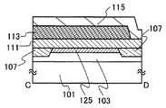
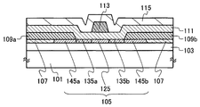
도 1a는 본 발명의 일 형태인 트랜지스터(100)의 구성을 설명하는 상면도이다. 도 1a의 일점쇄선 A-B 간의 단면도는 도 1b에 상당하고, 도 1a의 일점쇄선 C-D 간의 단면도는 도 1c에 상당하고, 도 1a의 일점쇄선 E-F 간의 단면도는 도 1d에 상당한다. 또한, 도 1a에 있어서, 하지 절연막(103), 게이트 절연막(111) 및 보호 절연막(115)은 명료화를 위해 도시하지 않고 있다.1A is a top view illustrating the configuration of a
도 1a 내지 도 1d로부터 트랜지스터(100)는 기판(101)과, 기판(101) 위에 설치된 하지 절연막(103)과, 하지 절연막(103) 위에 설치된 산화물 반도체막(105)과, 하지 절연막(103) 위이며, 또한 적어도 산화물 반도체막(105)의 측면과 접하여 설치된 사이드월 절연막(107)과, 산화물 반도체막(105) 및 사이드월 절연막(107) 위에 설치된 소스 전극(109a) 및 드레인 전극(109b)과, 산화물 반도체막(105)의 일부, 소스 전극(109a) 및 드레인 전극(109b)을 덮는 게이트 절연막(111)과, 게이트 절연막(111) 위이며, 또한 산화물 반도체막(105)과 중첩하는 게이트 전극(113)을 갖는 구조이다. 즉, 트랜지스터(100)는 톱 게이트-톱 콘택트 구조이다.1A to 1D, the
또한, 트랜지스터(100)는 산화물 반도체막(105)에 도펀트가 첨가된 영역과 도펀트가 첨가되어 있지 않은 영역을 갖는다. 구체적으로, 산화물 반도체막(105)은 게이트 전극(113)과 중첩하는 제1 산화물 반도체 영역(125)과, 한 쌍의 제2 산화물 반도체 영역(135a, 135b)과, 소스 전극(109a) 및 드레인 전극(109b)과 중첩하는 한 쌍의 제3 산화물 반도체 영역(145a, 145b)을 갖는다. 또한, 한 쌍의 제2 산화물 반도체 영역(135a, 135b)은 제1 산화물 반도체 영역(125)을 사이에 끼워서 설치되어 있다. 한 쌍의 제3 산화물 반도체 영역(145a, 145b)은 한 쌍의 제2 산화물 반도체 영역(135a, 135b)의 측면에 접하여 설치되어 있다. 그리고, 한 쌍의 제2 산화물 반도체 영역(135a, 135b)에는 도펀트가 첨가되어 있고, 제1 산화물 반도체 영역(125) 및 한 쌍의 제3 산화물 반도체 영역(145a, 145b)에는 도펀트가 첨가되어 있지 않다.In addition, the
한 쌍의 제2 산화물 반도체 영역(135a, 135b)에는 도펀트가 첨가되어 있는 점에서, 본 명세서에서는 한 쌍의 제2 산화물 반도체 영역(135a, 135b)을 LDD(Lightly Dope Drain) 영역이라고 부르기로 한다. 또한, 트랜지스터(100)에 있어서, 채널 형성되는 영역은 게이트 전극(113)과 중첩하는 제1 산화물 반도체 영역(125)이며, 한 쌍의 제3 산화물 반도체 영역(145a, 145b)은 소스 영역 및 드레인 영역이 된다.Since a dopant is added to the pair of second
트랜지스터(100)는 상기 구조에 대하여 추가로 게이트 절연막(111) 및 게이트 전극(113)을 덮는 보호 절연막(115)을 갖는 구조이어도 된다(도 1b 내지 도 1d 참조).The
이어서, 트랜지스터(100)의 하나의 변형예인 트랜지스터(110)에 대하여 설명한다. 도 2a는 트랜지스터(110)의 구성을 설명하는 상면도이다. 도 2a의 일점쇄선 A-B 간의 단면도는 도 2b에 상당하고, 도 2a의 일점쇄선 C-D 간의 단면도는 도 2c에 상당하고, 도 2a의 일점쇄선 E-F 간의 단면도는 도 2d에 상당한다. 또한, 도 2a에 있어서도, 하지 절연막(103), 게이트 절연막(111) 및 보호 절연막(115)은 명료화를 위해 도시하지 않고 있다.Next, the
도 2a 내지 도 2d로부터 트랜지스터(110)은 하지 절연막(103)의 형상이 트랜지스터(100)와 상이하다. 트랜지스터(110)의 하지 절연막(103)은 하지 절연막(103)의 산화물 반도체막(105)과 접하는 영역에 볼록부를 갖는 형상이다. 그 때문에, 트랜지스터(110)의 사이드월 절연막(107)은 하지 절연막(103) 위이며, 또한 적어도 산화물 반도체막(105)의 측면 및 하지 절연막(103)의 볼록부의 측면과 접하여 설치된다. 또한, 트랜지스터(110)의 다른 구성은 트랜지스터(100)와 동일하다.2A to 2D, the shape of the
이어서, 트랜지스터(100)의 하나의 변형예인 트랜지스터(130)에 대하여 설명한다. 도 3a는 트랜지스터(130)의 구성을 설명하는 상면도이다. 도 3a의 일점쇄선 A-B 간의 단면도는 도 3b에 상당하고, 도 3a의 일점쇄선 C-D 간의 단면도는 도 3c에 상당하고, 도 3a의 일점쇄선 E-F 간의 단면도는 도 3d에 상당한다. 또한, 도 3a에 있어서도, 하지 절연막(103), 게이트 절연막(111) 및 보호 절연막(115)은 명료화를 위해 도시하지 않고 있다.Next, the
도 3a 내지 도 3d로부터 트랜지스터(130)는 트랜지스터(110)와 마찬가지로 하지 절연막(103)의 형상이 트랜지스터(100)와 상이하고, 트랜지스터(130)의 하지 절연막(103)은 하지 절연막(103)의 산화물 반도체막(105)과 접하는 영역에 볼록부를 갖는 형상이다. 또한, 트랜지스터(130)는 서로 다른 2 이상의 절연막을 적층된 사이드월 절연막(107a, 107b)이 설치되어 있다. 사이드월 절연막(107a)은 하지 절연막(103) 위이며, 또한 적어도 산화물 반도체막(105)의 측면 및 하지 절연막(103)의 볼록부의 측면과 접하여 설치되어 있다. 사이드월 절연막(107b)은 사이드월 절연막(107a)에 접하여 설치되어 있다. 또한, 트랜지스터(130)의 다른 구성은 트랜지스터(100)와 동일하다.3A through 3D, the
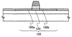
이어서, 트랜지스터(100)의 하나의 변형예인 트랜지스터(140)에 대하여 설명한다. 도 25a는 트랜지스터(140)의 구성을 설명하는 상면도이다. 도 25a의 일점쇄선 A-B 간의 단면도는 도 25b에 상당하고, 도 25a의 일점쇄선 C-D 간의 단면도는 도 25c에 상당하고, 도 25a의 일점쇄선 E-F 간의 단면도는 도 25의 (d)에 상당한다. 또한, 도 25a에 있어서도, 하지 절연막(103), 게이트 절연막(161) 및 보호 절연막(166)은 명료화를 위해 도시하지 않고 있다.Next, the
도 25a 내지 도 25의 (d)로부터 트랜지스터(140)은 산화물 반도체막(105)에 있어서의 도펀트가 첨가된 영역의 형상, 게이트 절연막(161)의 형상, 및 보호 절연막(166)의 형상이 트랜지스터(100)와 상이하다.25A to 25D, the
트랜지스터(140)의 산화물 반도체막(105)은 게이트 전극(113)과 중첩하는 제1 산화물 반도체 영역(125)과, 소스 전극(109a) 및 드레인 전극(109b)의 일부와 중첩하는 한 쌍의 제2 산화물 반도체 영역(165a, 165b)을 갖는다. 또한, 한 쌍의 제2 산화물 반도체 영역(165a, 165b)은 제1 산화물 반도체 영역(125)을 끼워서 설치되어 있다. 그리고, 한 쌍의 제2 산화물 반도체 영역(165a, 165b)에는 도펀트가 첨가되어 있다.The
또한, 트랜지스터(140)의 게이트 절연막(161)은 게이트 전극(113)과 중첩하는 영역에만 설치되어 있다. 이로 인해, 보호 절연막(166)의 일부는 산화물 반도체막(105)에 접하여 설치된다. 또한, 트랜지스터(140)의 다른 구성은 트랜지스터(100)와 동일하다.In addition, the
<트랜지스터(100)의 제조 방법><Method of
이어서, 도 1에 도시하는 트랜지스터(100)의 제조 방법에 대해서 도 4 내지 도 7을 사용하여 설명한다. 또한, 도 4 내지 도 7은 트랜지스터(100)의 제조 방법을 설명하는 단면도이며, 도 1a의 일점쇄선 A-B 간의 단면도에 상당한다.Next, the manufacturing method of the
기판(101) 위에 제1 절연막으로서 하지 절연막(103)을 형성한다.A
기판(101)은 재질 등에 큰 제한은 없지만, 적어도, 후의 열처리에 견딜 수 있을 정도의 내열성을 갖고 있는 필요가 있다. 예를 들어, 유리 기판, 세라믹 기판, 석영 기판, 사파이어 기판 등을, 기판(101)으로서 사용해도 된다.Although the board |
또한, 실리콘이나 탄화 실리콘 등의 단결정 반도체 기판, 다결정 반도체 기판, 실리콘 게르마늄 등의 화합물 반도체 기판, 금속 또는 스테인리스 등의 도전체으로 이루어지는 도전성 기판, 또는 이들 반도체 기판 또는 도전성 기판의 표면을 절연 재료로 피복한 기판 등을 사용할 수 있다. 또한, 이것들의 기판 위에 반도체 소자가 설치된 것을 기판(101)으로서 사용해도 된다.Furthermore, a single crystal semiconductor substrate such as silicon or silicon carbide, a polycrystalline semiconductor substrate, a compound semiconductor substrate such as silicon germanium, a conductive substrate made of a conductor such as metal or stainless steel, or a surface of these semiconductor substrates or conductive substrates is covered with an insulating material. One substrate or the like can be used. Moreover, you may use what provided the semiconductor element on these board | substrates as the board |
또한, 기판(101)으로서 가요성을 갖는 유리 기판 또는 가요성을 갖는 플라스틱 기판을 사용할 수 있다. 플라스틱 기판으로서는 굴절률 이방성이 작은 기판을 사용하는 것이 바람직하고, 대표적으로는 폴리에테르술폰(PES) 필름, 폴리이미드 필름, 폴리에틸렌나프탈레이트(PEN) 필름, PVF(폴리비닐 플루오라이드) 필름, 폴리에스테르 필름, 폴리카르보네이트(PC) 필름, 아크릴 수지 필름, 또는 반경화한 유기 수지 내에 섬유체를 포함하는 프리프레그 등을 사용할 수 있다.As the
하지 절연막(103)은 기판(101)으로부터의 불순물(예를 들어, Li나 Na 등의 알칼리 금속 등)의 확산을 방지하는 것 외에, 트랜지스터(100)의 제조 공정에서의 에칭 공정에 의해 기판(101)이 에칭되는 것을 방지한다.The base
또한, 하지 절연막(103)으로서는 산화실리콘, 산화갈륨, 산화알루미늄, 산화하프늄, 또는 산화이트륨 등의 산화물 절연막 재료를 단층 구조, 또는 이것들의 적층 구조로서 형성한다.As the
또한, 트랜지스터(100)의 제조에 있어서, Li나 Na 등의 알칼리 금속은 불순물이기 때문에 함유량을 적게 하는 것이 바람직하다. 기판(101)에 알칼리 금속 등의 불순물을 포함하는 유리 기판을 사용하는 경우, 알칼리 금속의 침입 방지를 위해 하지 절연막(103)을 적층 구조로서, 기판(101)과 접하는 절연막에 있어서, 질화실리콘, 또는 질화알루미늄 등의 질화물 절연막 재료를 사용하는 것이 바람직하다.In the manufacture of the
또한, 하지 절연막(103)은 적어도 표면에 산소를 포함하고, 상기 산소의 일부가 열처리에 의해 탈리하는 산화물 절연막을 사용하여 형성하는 것이 바람직하다. 산소의 일부가 열처리에 의해 탈리하는 산화물 절연막으로서는 화학양론비보다도 많은 산소를 포함하는 산화물 절연막이다. 이것은 열처리에 의해 하지 절연막(103)에 접하는 산화물 반도체막에 산소를 확산시킬 수 있기 때문이다.In addition, it is preferable to form the
하지 절연막(103)의 두께는 50 nm 이상, 바람직하게는 200 nm 이상 500 nm 이하, 더욱 바람직하게는 500 nm 이상 800 nm 이하로 한다. 하지 절연막(103)을 두껍게 함으로써 하지 절연막(103)의 산소 탈리량을 증가시킬 수 있음과 함께, 하지 절연막(103) 및 후에 형성되는 산화물 반도체막과의 계면에 있어서의 계면 준위를 저감하는 것이 가능하다.The thickness of the underlying insulating
여기서, 산화질화실리콘이란 그의 조성에 있어서 질소보다도 산소의 함유량이 많은 것을 나타내고, 예를 들어, 산소가 50 원자% 이상 70 원자% 이하, 질소가 0.5 원자% 이상 15 원자% 이하, 규소가 25 원자% 이상 35 원자% 이하, 수소가 0 원자% 이상 10 원자% 이하의 범위로 포함되는 것을 말한다. 또한, 질화산화실리콘이란 그의 조성에 있어서 산소보다도 질소의 함유량이 많은 것을 나타내고, 예를 들어, 산소가 5 원자% 이상 30 원자% 이하, 질소가 20 원자% 이상 55 원자% 이하, 규소가 25 원자% 이상 35 원자% 이하, 수소가 10 원자% 이상 25 원자% 이하의 범위로 포함되는 것을 말한다. 단, 상기 범위는 러더포드 후방 산란법(RBS: Rutherford Backscattering Spectrometry)이나, 수소 전방 산란법(HFS: Hydrogen Forward Scattering Spectrometry)을 사용하여 측정한 경우의 것이다. 또한, 구성 원소의 함유 비율은 그의 합계가 100 원자%를 초과하지 않는 값을 취한다.Here, silicon oxynitride shows that the content of oxygen is higher than nitrogen in its composition, for example, 50 atomic% or more and 70 atomic% or less of oxygen, 0.5 atomic% or more and 15 atomic% or less of silicon, and 25 atoms of silicon It means that it is contained in the range of 0 atomic% or more and 35 atomic% or less, and 0 atomic% or more and 10 atomic% or less. In addition, silicon nitride oxide shows that nitrogen content is larger than oxygen in the composition, for example, 5 atomic% or more and 30 atomic% or less, 20 atomic% or more and 55 atomic% or less, and 25 atomic atoms of silicon It means what is contained in the range of 10 atomic% or more and 35 atomic% or less and 10 atomic% or more and 25 atomic% or less. However, the range is measured by using Rutherford Backscattering Spectrometry (RBS) or Hydrogen Forward Scattering Spectrometry (HFS). In addition, the content rate of a structural element takes the value whose sum does not exceed 100 atomic%.
또한, 「산소의 일부가 열처리에 의해 탈리하는」이란 TDS(Thermal Desorption Spectroscopy: 승온 탈리 가스 분광법) 분석에서, 산소 원자로 환산한 산소의 방출량이 1.0×10¹⁸ atoms/㎤ 이상, 바람직하게는 3.0×10²⁰ atoms/㎤ 이상인 것을 말한다.In addition, "part of oxygen desorption by heat processing" means TDS (Thermal Desorption Spectroscopy) analysis, wherein the amount of oxygen released in terms of oxygen atoms is 1.0 × 10 18 atoms / cm 3 or more, preferably 3.0 × It means more than 10 20 atoms / cm 3.
이하, 산소의 방출량을 TDS 분석에서 산소 원자로 환산하여 정량하는 방법에 대하여 설명한다.Hereinafter, the method of quantifying the amount of oxygen released into oxygen atoms in TDS analysis will be described.
TDS 분석했을 때의 기체의 방출량은 스펙트럼의 적분값에 비례한다. 이로 인해, 절연막의 스펙트럼의 적분값과, 표준 시료의 기준값에 대한 비에 의해 기체의 방출량을 계산할 수 있다. 표준 시료의 기준값이란 소정의 원자를 포함하는 시료의, 스펙트럼의 적분값에 대한 원자의 밀도의 비율이다.The amount of gas released during TDS analysis is proportional to the integral of the spectrum. For this reason, the gas emission amount can be calculated by the ratio of the integral value of the spectrum of an insulating film, and the ratio with respect to the reference value of a standard sample. The reference value of the standard sample is the ratio of the density of atoms to the integrated value of the spectrum of the sample containing the predetermined atoms.
예를 들어, 표준 시료인 소정의 밀도의 수소를 포함하는 실리콘 웨이퍼의 TDS 분석 결과, 및 절연막의 TDS 분석 결과로부터, 절연막의 산소 분자의 방출량(NO2)은 수학식 1로 구할 수 있다. 여기서, TDS 분석에서 얻어지는 질량수 32로 검출되는 스펙트럼의 모두가 산소 분자 유래라고 가정한다. 질량수 32의 것으로서 CH3OH가 있지만, 존재할 가능성이 낮은 것으로서 여기에서는 고려하지 않는다. 또한, 산소 원자의 동위체인 질량수 17의 산소 원자 및 질량수 18의 산소 원자를 포함하는 산소 분자에 대해서도, 자연계에 있어서의 존재 비율이 극미량이기 때문에 고려하지 않는다.For example, from the results of TDS analysis of a silicon wafer containing hydrogen of a predetermined density, which is a standard sample, and of TDS analysis of an insulating film, the emission amount ( NO2 ) of oxygen molecules of the insulating film can be found by the following equation (1). Here, it is assumed that all of the spectra detected by the mass number 32 obtained by TDS analysis are derived from oxygen molecules. There is CH 3 OH as the mass number 32, but it is not considered here as it is unlikely to exist. In addition, the oxygen molecule containing the oxygen atom of the mass number 17 and the oxygen atom of the mass number 18 which is an isotope of an oxygen atom is also not considered because the existence ratio in nature is very small.
![]()
![]()
NH2는 표준 시료로부터 탈리한 수소 분자를 밀도로 환산한 값이다. SH2는 표준 시료를 TDS 분석했을 때의 스펙트럼의 적분값이다. 여기서, 표준 시료의 기준값을 NH2/SH2로 한다. SO2는 절연막을 TDS 분석했을 때의 스펙트럼의 적분값이다. α는 TDS 분석에 있어서의 스펙트럼 강도에 영향을 미치는 계수이다. 수학식 1의 상세 사항에 대해서는 일본 특허 공개 평6-275697 공보를 참조할 수 있다. 또한, 상기한 산소의 방출량의 수치는 덴시 가가꾸 가부시끼가이샤 제조의 승온 탈리 분석 장치 EMD-WA1000S/W를 사용하고, 표준 시료로서 1×10¹⁶ atoms/㎤의 수소 원자를 포함하는 실리콘 웨이퍼를 사용하여 측정한 수치이다.N H2 is a value obtained by converting the hydrogen molecule desorbed from the standard sample to the density. S H2 is the integral value of the spectrum when the TDS analysis of a standard sample is carried out. Here, the reference value of the standard sample is N H2 / S H2 . SO2 is an integral value of the spectrum when the insulating film is analyzed by TDS. α is a coefficient that affects the spectral intensity in the TDS analysis. For details of
또한, TDS 분석에 있어서, 산소의 일부는 산소 원자로서 검출된다. 산소 분자와 산소 원자의 비율은 산소 분자의 이온화율로부터 산출할 수 있다. 또한, 상술한 α는 산소 분자의 이온화율을 포함하기 때문에, 산소 분자의 방출량을 평가함으로써 산소 원자의 방출량에 대해서도 어림잡을 수 있다.In addition, in TDS analysis, part of oxygen is detected as an oxygen atom. The ratio of oxygen molecules and oxygen atoms can be calculated from the ionization rate of the oxygen molecules. In addition, since alpha mentioned above contains the ionization rate of an oxygen molecule, the emission amount of an oxygen atom can be estimated also by evaluating the emission amount of an oxygen molecule.
또한, NO2는 산소 분자의 방출량이다. 절연막에 있어서는 산소 원자로 환산했을 때의 산소의 방출량은 산소 분자의 방출량의 2배가 된다.In addition, N O2 is the amount of oxygen molecules released. In the insulating film, the amount of oxygen released when converted into oxygen atoms is twice the amount of released oxygen molecules.
산소의 일부가 열처리에 의해 탈리하는 산화물 절연막의 일례로서 화학양론비보다 과잉한 산소를 포함하는 산화물 절연막을 들 수 있고, 구체적으로는 산소가 과잉한 산화실리콘(SiOX(X>2))이다. 산소가 과잉한 산화실리콘(SiOX(X>2))이란 실리콘 원자수의 2배보다 많은 산소 원자를 단위 체적당에 포함하는 것이다. 단위 체적당의 실리콘 원자수 및 산소 원자수는 러더포드 후방 산란법에 의해 측정한 값이다.An example of an oxide insulating film in which a part of oxygen is released by heat treatment is an oxide insulating film containing oxygen in excess of the stoichiometric ratio, and specifically, silicon oxide (SiO X (X> 2)) in which oxygen is excessive. . Oxygen-rich silicon oxide (SiO X (X> 2)) includes more than twice as many oxygen atoms per unit volume of silicon atoms. The number of silicon atoms and oxygen atoms per unit volume is the value measured by Rutherford backscattering method.
하지 절연막(103)으로서 산소의 일부가 열처리에 의해 탈리하는 산화물 절연막을 사용함으로써 후에 형성되는 산화물 반도체막에 산소를 확산시켜, 하지 절연막(103) 및 상기 산화물 반도체막의 계면 준위를 저감할 수 있다. 따라서, 트랜지스터(100)의 동작에 기인하여 발생할 수 있는 전하 등이 하지 절연막(103) 및 상기 산화물 반도체막의 계면에 포획되는 것을 억제할 수 있어, 트랜지스터(100)를 전기 특성 열화가 적은 트랜지스터로 할 수 있다.By using an oxide insulating film in which a part of oxygen is released by heat treatment as the underlying insulating
하지 절연막(103)은 스퍼터링법, 또는 CVD법 등으로 형성할 수 있다. CVD법을 사용하는 경우에는 하지 절연막(103)을 형성한 후에 열처리를 행하여 하지 절연층(103)에 포함되는 수소 등을 탈리시켜서 제거하는 것이 바람직하다. 또한, 하지 절연막(103)이 산소의 일부가 열처리에 의해 탈리하는 산화물 절연막에 의해 형성되는 경우에는 스퍼터링법에 의한 형성 쪽이 행하기 쉽기 때문에 바람직하다.The base
하지 절연막(103)을 스퍼터링법에서 형성하는 경우, 실리콘 타깃, 석영 타깃, 알루미늄 타깃 또는 산화알루미늄 타깃 등을 사용하여, 산소를 포함하는 분위기 가스 중에서 형성하면 된다. 분위기 가스 중의 산소의 비율은 분위기 가스 전체에 대하여 6 체적% 이상으로 한다. 바람직하게는 50 체적% 이상으로 한다. 분위기 가스 중의 산소 가스의 비율을 높임으로써 산소의 일부가 열처리에 의해 탈리하는 산화물 절연막을 형성할 수 있다.When the
타깃 내의 수소도 최대한 제거되어 있으면 바람직하다. 구체적으로는 OH기가 100 ppm 이하, 바람직하게는 10 ppm 이하, 보다 바람직하게는 1 ppm 이하의 산화물 타깃을 사용함으로써 하지 절연막(103)의 수소 농도를 저감하여 트랜지스터(100)의 전기 특성 및 신뢰성을 높일 수 있다. 예를 들어, 용융 석영은 OH기가 10 ppm 이하로 하기 쉽고, 또한 비용이 낮기 때문에 바람직하다. 물론 OH기 농도가 낮은 합성 석영의 타깃을 사용해도 된다.It is preferable that hydrogen in a target is removed as much as possible. Specifically, by using an oxide target having an OH group of 100 ppm or less, preferably 10 ppm or less, more preferably 1 ppm or less, the hydrogen concentration of the underlying insulating
이어서, 하지 절연막(103) 위에 제1 산화물 반도체막(120)을 형성한다(도 4a 참조). 하지 절연막(103) 위에 스퍼터링법, 분자선 애피택시법, 원자층 퇴적법 또는 펄스 레이저 증착법에 의해 제1 산화물 반도체막(120)이 얻어진다. 여기에서는 스퍼터링법에 의해 제1 산화물 반도체막(120)을 형성한다. 제1 산화물 반도체막(120)은 두께 1 nm 이상 50 nm 이하로 형성하면 된다.Subsequently, a first
제1 산화물 반도체막(120)은 In, Ga, Sn 및 Zn으로부터 선택된 하나 이상의 원소를 포함하는 금속 산화물을 사용할 수 있다. 또한, 상기 금속 산화물은 밴드갭이 2 eV 이상, 바람직하게는 2.5 eV 이상, 보다 바람직하게는 3 eV 이상의 것을 사용한다. 이와 같이, 밴드갭이 넓은 금속 산화물을 사용함으로써 트랜지스터(100)의 오프 전류를 저감할 수 있다.The first
예를 들어, 제1 산화물 반도체막(120)로서 4원계 금속 산화물인 In-Sn-Ga-Zn계 산화물 반도체나, 3원계 금속 산화물인 In-Ga-Zn계 산화물 반도체, In-Sn-Zn계 산화물 반도체, In-Al-Zn계 산화물 반도체, Sn-Ga-Zn계 산화물 반도체, Al-Ga-Zn계 산화물 반도체, Sn-Al-Zn계 산화물 반도체나, 2원계 금속 산화물인 In-Zn계 산화물 반도체, Sn-Zn계 산화물 반도체, Al-Zn계 산화물 반도체, Zn-Mg계 산화물 반도체, Sn-Mg계 산화물 반도체, In-Mg계 산화물 반도체나, In-Ga계의 재료, 일원계 금속 산화물인 산화인듐, 산화주석, 산화아연 등을 사용할 수 있다. 또한, n원계 금속 산화물은 n 종류의 금속 산화물로 구성되는 것으로 한다. 여기서, 예를 들어, 3원계 금속 산화물인 In-Ga-Zn계 산화물 반도체는 인듐(In), 갈륨(Ga), 아연(Zn)을 갖는 산화물이라고 하는 의미이며, 그의 조성비는 특별히 상관없다. 또한, In과 Ga과 Zn 이외의 원소를 포함하고 있어도 된다.For example, as the first
또한, 상기 금속 산화물에서는 이것들의 화학양론비에 대하여 산소(O)를 과잉으로 포함시키는 것이 바람직하다. 산소(O)를 과잉으로 포함시키면 형성되는 제1 산화물 반도체막(120)의 산소 결손에 의한 캐리어의 생성을 억제할 수 있다.In the metal oxide, it is preferable to include oxygen (O) excessively with respect to these stoichiometric ratios. When oxygen (O) is excessively included, generation of carriers due to oxygen vacancies in the formed first
또한, 제1 산화물 반도체막(120)로서 화학식 InMO3(ZnO)m(m>0)로 표기되는 산화물 반도체를 사용할 수 있다. 여기서, M은 Zn, Ga, Al, Mn 및 Co로부터 선택된 하나 또는 복수의 금속 원소를 나타낸다. 예를 들어 M으로서 Ga, Ga 및 Al, Ga 및 Mn, 또는 Ga 및 Co 등이 있다.As the first
또한, 제1 산화물 반도체막(120)로서 In-Zn계 산화물 반도체를 사용하는 경우, 사용하는 타깃의 조성비는 원자수비로 In:Zn=50:1 내지 1:2(몰수비로 환산하면 In2O3:ZnO=25:1 내지 1:4), 바람직하게는 In:Zn=20:1 내지 1:1(몰수비로 환산하면 In2O3:ZnO=10:1 내지 1:2), 더욱 바람직하게는 In:Zn=1.5:1 내지 15:1(몰수비로 환산하면 In2O3:ZnO=3:4 내지 15:2)로 한다. 예를 들어, In-Zn계 산화물 반도체의 형성에 사용하는 타깃은 원자수비가 In:Zn:O=X:Y:Z인 때, Z>1.5X+Y로 한다.Furthermore, the first oxide when using the In-Zn-based oxide semiconductor as a
또한, 제1 산화물 반도체막(120)은 비정질한 산화물 반도체막이어도, 결정 영역을 포함하는 산화물 반도체막이어도 된다.The first
여기서, 제1 산화물 반도체막(120)을 형성하는 스퍼터링 장치에 대해서 이하에 상세 사항을 설명한다.Here, the sputtering apparatus for forming the first
제1 산화물 반도체막(120)을 형성하는 처리실은 누설 레이트를 1×10⁻¹⁰ Pa·㎥/초 이하로 하는 것이 바람직하고, 그것에 의해 스퍼터링법에 의해 형성할 때, 막 내로의 불순물의 혼입을 저감할 수 있다.The process chamber for forming the first
누설 레이트를 낮게 하기 위해서는 외부 누설뿐만아니라 내부 누설을 저감할 필요가 있다. 외부 누설이란 미소한 구멍이나 시일 불량 등에 의해 진공계의 밖으로부터 기체가 유입하는 것이다. 내부 누설이란 진공계 내의 밸브 등의 구획으로부터의 누설이나 내부의 부재로부터의 방출 가스에 기인한다. 누설 레이트를 1×10⁻¹⁰ Pa·㎥/초 이하로 하기 위해서는 외부 누설 및 내부 누설의 양면으로부터 대책을 취할 필요가 있다.In order to lower the leak rate, it is necessary to reduce not only external leakage but also internal leakage. External leakage refers to the inflow of gas from the outside of the vacuum system due to a small hole or a poor seal. Internal leakage is due to leakage from compartments such as valves in a vacuum system or discharge gas from internal members. In order to set the leak rate to 1 × 10 -10 Pa · m 3 / sec or less, it is necessary to take measures from both sides of the external leakage and the internal leakage.
외부 누설을 저감시키기 위해서는 처리실의 개폐 부분은 메탈 가스킷으로 시일하면 된다. 메탈 가스킷은 불화철, 산화알루미늄, 또는 산화크롬에 의해 피복된 금속 재료를 사용하면 바람직하다. 메탈 가스킷은 O링과 비교하여 밀착성이 높아, 외부 누설을 저감할 수 있다. 또한, 불화철, 산화알루미늄, 산화크롬 등의 부동태에 의해 피복된 금속 재료를 사용함으로써 메탈 가스킷으로부터 발생하는 수소를 포함하는 방출 가스가 억제되어, 내부 누설도 저감할 수 있다.In order to reduce external leakage, the opening and closing portion of the processing chamber may be sealed with a metal gasket. It is preferable to use a metal material coated with iron fluoride, aluminum oxide, or chromium oxide as the metal gasket. Metal gaskets have high adhesion compared to O-rings and can reduce external leakage. In addition, by using a metal material coated by a passivation such as iron fluoride, aluminum oxide, and chromium oxide, the release gas containing hydrogen generated from the metal gasket can be suppressed, and the internal leakage can also be reduced.
처리실의 내벽으로서 사용하는 부재는 수소를 포함하는 방출 가스가 적은 알루미늄, 크롬, 티타늄, 지르코늄, 니켈 또는 바나듐 또는 이들을 철, 크롬 및 니켈 등 중 적어도 하나를 포함하는 합금 재료에 피복한 것을 사용해도 된다. 철, 크롬 및 니켈 등 중 적어도 하나를 포함하는 합금 재료는 강성이 있고, 열에 강하고, 또한 가공에 적합하다. 여기서, 처리실의 내벽의 표면적을 작게 하기 위해서, 상기 부재의 표면 요철을 연마 등에 의해 저감해 두면, 방출 가스를 저감할 수 있다. 또는 상기 부재를 불화철, 산화알루미늄, 산화크롬 등의 부동태로 피복해도 된다.The member used as the inner wall of the processing chamber may be one in which aluminum, chromium, titanium, zirconium, nickel or vanadium containing a small amount of emission gas containing hydrogen is coated on an alloy material containing at least one of iron, chromium and nickel. . Alloy materials including at least one of iron, chromium, nickel, and the like are rigid, resistant to heat, and suitable for processing. Here, in order to reduce the surface area of the inner wall of the processing chamber, if the surface irregularities of the member are reduced by polishing or the like, the emission gas can be reduced. Alternatively, the member may be coated with a passivation agent such as iron fluoride, aluminum oxide, and chromium oxide.
또한, 분위기 가스를 처리실에 도입하기 직전에 분위기 가스의 정제기를 설치하는 것이 바람직하다. 이때, 정제기로부터 처리실까지의 배관의 길이를 5 m 이하, 바람직하게는 1 m 이하로 한다. 배관의 길이를 5 m 이하 또는 1 m 이하로 함으로써 배관으로부터의 방출 가스의 영향을 길이에 따라서 저감할 수 있다.In addition, it is preferable to provide a purifier of the atmospheric gas immediately before introducing the atmospheric gas into the processing chamber. At this time, the length of the pipe from the refiner to the processing chamber is 5 m or less, preferably 1 m or less. By setting the length of the pipe to 5 m or less or 1 m or less, the influence of the discharged gas from the pipe can be reduced along the length.
처리실의 배기는 드라이 펌프 등의 조연줄 펌프와, 스퍼터 이온 펌프, 터보 분자 펌프 및 크라이오 펌프 등의 고진공 펌프를 적절하게 조합하여 행하면 된다. 터보 분자 펌프는 큰 크기의 분자의 배기가 우수한 한편, 수소나 물의 배기 능력이 낮다. 따라서, 물의 배기 능력이 높은 크라이오 펌프 및 수소의 배기 능력이 높은 스퍼터 이온 펌프를 조합하는 것이 유효하게 된다.The evacuation of the processing chamber may be performed by appropriately combining a string pump such as a dry pump and a high vacuum pump such as a sputter ion pump, a turbo molecular pump, and a cryopump. Turbomolecular pumps are good at exhausting large-sized molecules while having low capacity for hydrogen or water. Therefore, it becomes effective to combine a cryopump with a high water exhaust capability and a sputter ion pump with a high exhaust capacity of hydrogen.
처리실 내에 존재하는 흡착물은 내벽에 흡착하고 있기 때문에 처리실의 압력에 영향을 미치지 않지만, 처리실을 배기했을 때의 가스 방출의 원인이 된다. 그 때문에, 누설 레이트와 배기 속도에 상관은 없지만, 배기 능력이 높은 펌프를 사용하여 처리실에 존재하는 흡착물을 가능한 한 탈리하고, 미리 배기해 두는 것이 중요하다. 또한, 흡착물의 탈리를 촉진하기 위해서 처리실을 베이킹해도 된다. 베이킹 함으로써 흡착물의 탈리 속도를 10배 정도 크게 할 수 있다. 베이킹은 100℃ 이상 450℃ 이하에서 행하면 된다. 이때, 불활성 가스를 도입하면서 흡착물의 제거를 행하면, 배기하는 것만으로는 탈리하기 어려운 물 등의 탈리 속도를 더욱 크게 할 수 있다.Since the adsorbate present in the processing chamber is adsorbed on the inner wall, it does not affect the pressure in the processing chamber, but it is the cause of gas discharge when the processing chamber is evacuated. Therefore, regardless of the leak rate and the exhaust speed, it is important to detach the adsorbate present in the process chamber as much as possible and to evacuate it in advance using a pump having high exhaust capacity. Moreover, you may bake a process chamber in order to accelerate | release the adsorbate. By baking, the desorption rate of an adsorbate can be made about 10 times larger. What is necessary is just to bake at 100 to 450 degreeC. At this time, if the adsorbate is removed while introducing an inert gas, it is possible to further increase the desorption rate of water or the like that is difficult to be desorbed only by evacuation.
스퍼터링법에 있어서, 플라즈마를 발생시키기 위한 전원 장치는 RF 전원 장치, AC 전원 장치, DC 전원 장치 등을 적절하게 사용할 수 있다.In the sputtering method, a power supply device for generating plasma can be suitably used an RF power supply device, an AC power supply device, a DC power supply device, or the like.
제1 산화물 반도체막(120)을 스퍼터링법에서 형성할 때가 타깃으로서는 In, Ga, Sn 및 Zn으로부터 선택된 하나 이상의 원소를 포함하는 금속 산화물 타깃을 사용할 수 있다. 타깃으로서는 4원계 금속 산화물인 In-Sn-Ga-Zn계 금속 산화물이나, 3원계 금속 산화물인 In-Ga-Zn계 금속 산화물, In-Sn-Zn계 금속 산화물, In-Al-Zn계 금속 산화물, Sn-Ga-Zn계 금속 산화물, Al-Ga-Zn계 금속 산화물, Sn-Al-Zn계 금속 산화물이나, 2원계 금속 산화물인 In-Zn계 금속 산화물, Sn-Zn계 금속 산화물 등의 타깃을 사용할 수 있다.When the first
타깃의 일례로서 In, Ga, 및 Zn을 포함하는 금속 산화물 타깃은 In2O3:Ga2O3:ZnO=1:1:1 [mol수비]의 조성비를 갖는다. 또한, 상기 금속 산화물 타깃은 In2O3:Ga2O3:ZnO=1:1:2 [mol수비]의 조성비를 갖는 타깃, 또는 In2O3:Ga2O3:ZnO=1:1:4 [mol수비]의 조성비를 갖는 타깃, In2O3:Ga2O3:ZnO=2:1:8 [mol수비]의 조성비를 갖는 타깃을 사용할 수도 있다.As an example of the target, the metal oxide target containing In, Ga, and Zn has a composition ratio of In 2 O 3 : Ga 2 O 3 : ZnO = 1: 1: 1 [mol ratio]. In addition, the metal oxide target is a target having a composition ratio of In 2 O 3 : Ga 2 O 3 : ZnO = 1: 1: 2 [mol ratio], or In 2 O 3 : Ga 2 O 3 : ZnO = 1: 1 A target having a composition ratio of: 4 [mol ratio] and a target having a composition ratio of In 2 O 3 : Ga 2 O 3 : ZnO = 2: 1: 8 [mol ratio] can also be used.
또한, 제1 산화물 반도체막(120)로서 In-Zn계 산화물 반도체를 사용하는 경우, 사용하는 타깃의 조성비는 원자수비로 In:Zn=50:1 내지 1:2(몰수비로 환산하면 In2O3:ZnO=25:1 내지 1:4), 바람직하게는 In:Zn=20:1 내지 1:1(몰수비로 환산하면 In2O3:ZnO=10:1 내지 1:2), 더욱 바람직하게는 In:Zn=1.5:1 내지 15:1(몰수비로 환산하면 In2O3:ZnO=3:4 내지 15:2)로 한다. 예를 들어, In-Zn계 산화물 반도체의 형성에 사용하는 타깃은 원자수비가 In:Zn:O=X:Y:Z인 때, Z>1.5X+Y로 한다.Furthermore, the first oxide when using the In-Zn-based oxide semiconductor as a
또한, 분위기 가스는 희가스(대표적으로는 아르곤) 분위기, 산소 분위기, 희가스 및 산소의 혼합 가스를 적절하게 사용한다. 또한, 분위기 가스에는 수소, 물, 수산기 또는 수소화물 등의 불순물이 제거된 고순도 가스를 사용하는 것이 바람직하다.In addition, the atmosphere gas suitably uses a rare gas (typically argon) atmosphere, an oxygen atmosphere, a rare gas and a mixed gas of oxygen. In addition, it is preferable to use the high purity gas which remove | eliminated impurities, such as hydrogen, water, a hydroxyl group, or a hydride, for atmospheric gas.
상기 스퍼터링 장치를 사용함으로써 수소의 혼입이 저감된 제1 산화물 반도체막(120)을 형성할 수 있다. 또한, 상기 스퍼터링 장치를 사용해도, 제1 산화물 반도체막(120)은 적지 않게 질소를 포함하여 형성된다. 예를 들어, 2차 이온 질량 분석법(SIM: Secondary Ion Mass Spectroscopy)으로 측정되는 제1 산화물 반도체막(120)의 질소 농도는 5×10¹⁸ atoms/㎤ 미만이 된다.By using the sputtering apparatus, it is possible to form the first
또한, 하지 절연막(103) 및 제1 산화물 반도체막(120)은 진공 하에서 연속하여 형성해도 된다. 예를 들어, 기판(101) 표면의 수소를 포함하는 불순물을, 열처리 또는 플라즈마 처리로 제거한 후, 대기에 폭로하지 않고 하지 절연막(103)을 형성하고, 계속하여 대기에 폭로하지 않고 제1 산화물 반도체막(120)을 형성해도 된다. 이렇게 함으로써 기판(101) 표면의 수소를 포함하는 불순물을 저감하고 또한 기판(101)과 하지 절연막(103)의 계면, 하지 절연막(103)과 제1 산화물 반도체막(120)의 계면에 대기 성분이 부착되는 것을 억제할 수 있다. 그 결과, 트랜지스터(100)를 전기 특성이 양호하고, 신뢰성이 우수한 트랜지스터로 할 수 있다.The base
또한, 제1 산화물 반도체막(120)을 형성할 때 또는 형성 후에 있어서, 제1 산화물 반도체막(120)의 산소 결손에 기인하여 전하가 발생하는 경우가 있다. 제1 산화물 반도체막(120)의 산소 결손은 그 산소 결손의 일부가 도너가 되어 캐리어인 전자가 발생하기 때문에, 트랜지스터(100)의 임계값 전압을 마이너스 방향으로 변동시켜버린다.In addition, when the first
따라서, 제1 산화물 반도체막(120)을 형성 후에, 제1 열처리를 행하여 제2 산화물 반도체막(122)을 형성한다(도 4b 참조).Therefore, after the first
제1 열처리는 제1 산화물 반도체막(120)으로부터 수소(물, 수산기 또는 수소화물을 포함함)을 방출시킴과 함께, 하지 절연막(103)에 포함되는 산소의 일부를 탈리시켜, 제1 산화물 반도체막(120) 내, 및 하지 절연막(103)과 제1 산화물 반도체막(120)의 계면 근방에 상기 산소를 확산시킨다.The first heat treatment releases hydrogen (including water, hydroxyl groups, or hydrides) from the first
제1 열처리의 온도는 상기한 산소의 확산을 가능하게 하는 온도로서, 구체적으로는 150℃ 이상 기판 변형점 온도 미만, 바람직하게는 250℃ 이상 450℃ 이하, 더욱 바람직하게는 300℃ 이상 450℃ 이하로 하고, 산화성 분위기 또는 불활성 분위기에서 행한다. 여기서, 산화성 분위기는 산소, 오존 또는 질화산소 등의 산화성 가스를 10 ppm 이상 함유하는 분위기를 말한다. 또한, 불활성 분위기는 전술한 산화성 가스가 10 ppm 미만이고, 그 외, 질소 또는 희가스로 충전된 분위기를 말한다. 처리 시간은 3분 내지 24시간으로 한다. 24시간을 초과하는 열처리는 생산성의 저하를 초래하기 때문에 바람직하지 않다.The temperature of the first heat treatment is a temperature that enables the diffusion of the oxygen, specifically 150 ° C or more and less than the substrate strain point temperature, preferably 250 ° C or more and 450 ° C or less, more preferably 300 ° C or more and 450 ° C or less. And an oxidizing atmosphere or an inert atmosphere. Here, an oxidative atmosphere means the atmosphere containing 10 ppm or more of oxidizing gases, such as oxygen, ozone, or oxygen nitride. Inert atmosphere refers to an atmosphere in which the above-described oxidizing gas is less than 10 ppm and filled with nitrogen or a rare gas. The treatment time is 3 minutes to 24 hours. Heat treatment over 24 hours is not preferable because it leads to a decrease in productivity.
제1 열처리에 사용하는 열처리 장치에 특별한 한정은 없고, 저항 발열체 등의 발열체로부터의 열전도 또는 열복사에 의해 피처리물을 가열하는 장치를 구비하고 있어도 된다. 예를 들어, 전기로나, GRTA(Gas Rapid Thermal Anneal) 장치, LRTA(Lamp Rapid Thermal Anneal) 장치 등의 RTA(Rapid Thermal Anneal) 장치를 사용할 수 있다. LRTA 장치는 할로겐 램프, 메탈 할라이드 램프, 크세논 아크 램프, 카본 아크 램프, 고압 나트륨 램프, 고압 수은 램프 등의 램프로부터 발하는 광(전자파)의 복사에 의해 피처리물을 가열하는 장치이다. GRTA 장치는 고온의 가스를 사용하여 열처리를 행하는 장치이다.There is no restriction | limiting in particular in the heat processing apparatus used for a 1st heat processing, The apparatus which heats a to-be-processed object by heat conduction or heat radiation from a heat generating body, such as a resistive heat generating body, may be provided. For example, an electric furnace or a Rapid Thermal Anneal (RTA) device such as a Gas Rapid Thermal Anneal (GRTA) device or a Lamp Rapid Thermal Anneal (LRTA) device may be used. The LRTA apparatus is an apparatus for heating a target object by radiation of light (electromagnetic waves) emitted from lamps such as halogen lamps, metal halide lamps, xenon arc lamps, carbon arc lamps, high pressure sodium lamps, and high pressure mercury lamps. GRTA apparatus is a apparatus which heat-processes using high temperature gas.
제1 열처리는 하지 절연막(103)에 포함되는 산소의 일부를 탈리시켜, 제1 산화물 반도체막(120) 내 및 하지 절연막(103)과 제1 산화물 반도체막(120)의 계면 근방에 상기 산소를 확산시키는 점에서, 제1 산화물 반도체막(120)의 산소 결손을 보충한다. 즉, 하지 절연막(103)으로부터 제1 산화물 반도체막(120)에 산소가 충분히 확산됨으로써, 임계값 전압을 마이너스 방향으로 변동시키는 제1 산화물 반도체막(120)의 산소 결손을 보충할 수 있다.The first heat treatment desorbs a part of oxygen included in the
또한, 제1 산화물 반도체막(120) 내의 수소는 도너가 되어 캐리어인 전자를 발생한다. 제1 열처리에 의해 제1 산화물 반도체막(120)은 막 내의 수소 농도가 저감되어, 고순도화된 제2 산화물 반도체막(122)이 된다. 따라서, 제2 산화물 반도체막(122)의 수소 농도는 5×10¹⁸ atoms/㎤ 미만, 바람직하게는 1×10¹⁸ atoms/㎤ 이하, 보다 바람직하게는 5×10¹⁷ atoms/㎤ 이하, 더욱 바람직하게는 1×10¹⁶ atoms/㎤ 이하이다. 또한, 제2 산화물 반도체막(122) 내의 수소 농도는 2차 이온 질량 분석법(SIMS: Secondary Ion Mass Spectroscopy)으로 측정되는 것이다.In addition, hydrogen in the first
제1 열처리에 의해 수소 농도가 충분히 저감되어서 고순도화되고, 또한 충분한 산소가 공급되어서 산소 결손에 기인하는 에너지갭 내의 결함 준위가 저감된 제2 산화물 반도체막(122)에서는 수소 등의 도너에 기인하는 캐리어 밀도가 1×10¹³/㎤ 이하가 된다. 또한, 실온(25℃)에서의 오프 전류(여기서는 단위 채널 폭(1 ㎛)당의 값)은 100 zA(1 zA(젭토 암페어)는 1×10-21 A) 이하, 바람직하게는 10 zA 이하가 된다. 제2 산화물 반도체막(122)을 사용함으로써 매우 우수한 오프 전류 특성의 트랜지스터(100)를 얻을 수 있다. 또한, Li나 Na 등의 알칼리 금속은 불순물이기 때문에 함유량을 적게 하는 것이 바람직하고 또한 제2 산화물 반도체막(122) 내에 2×1016 cm-3 이하, 바람직하게는 1×1015 cm-3 이하의 농도로 한다. 또한, 알칼리 토금속도 불순물이기 때문에, 함유량을 적게 하는 것이 바람직하다.In the second
상기로부터, 제1 열처리는 트랜지스터(100)의 전기 특성 및 신뢰성을 양호하게 할 수 있다.From the above, the first heat treatment can improve the electrical characteristics and the reliability of the
계속해서, 제2 산화물 반도체막(122)에 제1 포토리소그래피 공정을 행하여 제2 산화물 반도체막(122) 위에 레지스트 마스크를 형성한다. 상기 레지스트 마스크를 사용하여, 제1 에칭 공정에서 제2 산화물 반도체막(122)을 가공하여 제3 산화물 반도체막(124)을 형성한다(도 4c 참조). 또한, 상기 레지스트 마스크는 포토리소그래피 공정의 이외에 잉크젯법, 인쇄법 등을 적절하게 사용할 수 있다.Subsequently, a first photolithography process is performed on the second
제1 에칭 공정에 있어서, 제3 산화물 반도체막(124)의 단부가 테이퍼형 형상으로 되도록 에칭하는 것이 바람직하다. 제3 산화물 반도체막(124)의 단부를 테이퍼 형상으로 함으로써 후에 사이드월 절연막(107)이 될 제2 절연막(117)의 피복성을 향상시킬 수 있다. 포토리소그래피 공정을 사용하는 경우에는 레지스트 마스크를 후퇴시키면서 에칭함으로써 테이퍼 형상으로 할 수 있다.In the first etching step, the end portion of the third
제1 에칭 공정은 건식 에칭 또는 습식 에칭이어도 되고, 이것들을 조합하여 행해도 된다. 습식 에칭용의 에칭액으로서는 인산과 아세트산과 질산을 섞은 용액, 암모니아과수(31 중량% 과산화수소수:28 중량% 암모니아수:물=5:2:2(체적비)) 등을 사용할 수 있다. 또한, ITO07N(간또 가가꾸사제)을 사용해도 된다.Dry etching or wet etching may be sufficient as a 1st etching process, and you may perform combining these. As the etching solution for wet etching, a solution in which phosphoric acid, acetic acid and nitric acid are mixed, ammonia and water (31% by weight hydrogen peroxide: 28% by weight ammonia water: water = 5: 2: 2 (volume ratio)) and the like can be used. Moreover, you may use ITO07N (made by Kanto Chemical Co., Ltd.).
건식 에칭에 사용하는 에칭 가스로서는 염소를 포함하는 가스(염소계 가스, 예를 들어 염소(Cl2), 삼염화붕소(BCl3), 사염화규소(SiCl4), 사염화탄소(CCl4) 등)이 바람직하다.As an etching gas used for dry etching, a gas containing chlorine (chlorine-based gas such as chlorine (Cl 2 ), boron trichloride (BCl 3 ), silicon tetrachloride (SiCl 4 ), carbon tetrachloride (CCl 4 , etc.)) is preferable. .
또한, 불소를 포함하는 가스(불소계 가스, 예를 들어 사불화탄소(CF4), 육불화황(SF6), 삼불화질소(NF3), 트리플루오로메탄(CHF3) 등), 브롬화수소(HBr), 산소(O2), 이것들의 가스에 헬륨(He)이나 아르곤(Ar) 등의 희가스를 첨가한 가스 등을 사용할 수 있다.In addition, fluorine-containing gases (fluorine-based gases such as carbon tetrafluoride (CF 4 ), sulfur hexafluoride (SF 6 ), nitrogen trifluoride (NF 3 ), trifluoromethane (CHF 3 ), and hydrogen bromide) (HBr), oxygen (O 2 ), or a gas obtained by adding a rare gas such as helium (He) or argon (Ar) to these gases can be used.
건식 에칭으로서는 평행 평판형 RIE(Reactive Ion Etching)법이나, ICP(Inductively Coupled Plasma: 유도 결합형 플라즈마) 에칭법을 사용할 수 있다. 원하는 형상으로 가공할 수 있도록, 에칭 조건(코일형의 전극에 인가되는 전력량, 기판측의 전극에 인가되는 전력량, 기판측의 전극 온도 등)을 적절하게 조절한다.As dry etching, a parallel plate-type reactive ion etching (RIE) method or an inductively coupled plasma (ICP) etching method can be used. The etching conditions (the amount of power applied to the coil-shaped electrode, the amount of power applied to the electrode on the substrate side, the electrode temperature on the substrate side, etc.) are appropriately adjusted so as to be processed into a desired shape.
제3 산화물 반도체막(124)을 형성한 후, 상기 레지스트 마스크를 제거한다. 이때, 약액(박리액)을 사용하여 제거해도 되지만, 산소 플라즈마에 의한 애싱을 행하여 상기 레지스트 마스크를 제거해도 된다. 상기 레지스트 마스크의 제거를 산소 플라즈마에 의한 애싱으로 행함으로써 상기 약액에 의한 제3 산화물 반도체막(124) 표면의 오염을 억제할 수 있고, 산소 플라즈마에 의해 제3 산화물 반도체막(124)에 산소를 공급할 수 있다.After the third
제3 산화물 반도체막(124)과 같이, 원하는 형상으로 가공된 산화물 반도체막은 상기 산화물 반도체막의 측면이 활성이다. 또한, 활성이란 부대결합손을 갖고, 불안정한 결합 상태라고 하는 의미이다. 상기 산화물 반도체막의 측면이 활성인 것은 이하의 현상에 의해 발생하기 때문이다.As in the third
산화물 반도체막을 원하는 형상으로 가공할 때, 예를 들어, 상술한 조건에서 건식 에칭을 할 때, 산화물 반도체막의 측면이 염소 라디칼, 불소 라디칼 등을 포함하는 플라즈마에 노출되면, 산화물 반도체막의 측면에 노출되는 금속 원자와, 염소 라디칼, 불소 라디칼 등이 결합한다. 이때, 금속 원자와 염소 원자, 불소 원자가 결합하여 탈리하기 때문에, 산화물 반도체막 내에 상기 금속 원자와 결합하고 있었던 산소 원자가 활성이 된다. 활성이 된 산소 원자는 용이하게 반응하고, 탈리하기 쉽다. 그 때문에, 산화물 반도체막의 측면에는 산소 결손이 발생하기 쉽다.When the oxide semiconductor film is processed into a desired shape, for example, when dry etching is performed under the above-described conditions, when the side surface of the oxide semiconductor film is exposed to a plasma containing chlorine radicals, fluorine radicals, or the like, the side surface of the oxide semiconductor film is exposed. A metal atom, a chlorine radical, a fluorine radical, etc. combine. At this time, since the metal atom, the chlorine atom, and the fluorine atom are combined and released, the oxygen atom which has been bonded to the metal atom in the oxide semiconductor film becomes active. Activated oxygen atoms easily react and are easily detached. Therefore, oxygen deficiency tends to occur on the side surface of the oxide semiconductor film.
그리고, 원하는 형상으로 가공된 산화물 반도체막의 측면이 활성이면, 감압 분위기 또는 환원 분위기에 있어서, 산소가 빠져나가, 상기 산화물 반도체막의 측면에서 산소 결손을 발생한다. 감압 분위기 또는 환원 분위기는 막의 형성, 열처리 또는 건식 에칭 등, 트랜지스터의 제조 공정에서 빈번히 사용되는 처리 분위기이며, 특히 열처리된 분위기에서는 상기 산화물 반도체막의 측면에서 산소 결손이 발생하기 쉽다. 또한, 그의 산소 결손의 일부는 도너가 되어 캐리어인 전자를 생성하기 때문에, 상기 산화물 반도체막의 측면은 n형화한다.And if the side surface of the oxide semiconductor film processed into the desired shape is active, oxygen will escape in a reduced pressure atmosphere or a reducing atmosphere, and oxygen deficiency will generate | occur | produce in the side surface of the said oxide semiconductor film. A reduced pressure atmosphere or a reducing atmosphere is a processing atmosphere frequently used in a transistor manufacturing process, such as film formation, heat treatment, or dry etching. In particular, in a heat treated atmosphere, oxygen deficiency is likely to occur on the side of the oxide semiconductor film. In addition, since part of the oxygen vacancies becomes a donor to generate electrons as carriers, the side surfaces of the oxide semiconductor film are n-typed.
트랜지스터의 소스 전극 및 드레인 전극이 n형화한 측면을 포함하는 산화물 반도체막의 측면과 접함으로써 상기 산화물 반도체막의 측면을 통하여 소스 전극 및 드레인 전극 간에 누설 전류가 발생한다. 상기 누설 전류는 트랜지스터의 오프 전류를 증가시킨다. 또한, 상기 산화물 반도체막의 측면을 통하여 흐르는 전류는 경우에 따라 산화물 반도체막의 측면을 채널 영역으로 하는 트랜지스터를 형성하는 경우가 있다.A leakage current is generated between the source electrode and the drain electrode through the side surface of the oxide semiconductor film by contacting the side surface of the oxide semiconductor film including the n-sided side of the transistor source and drain electrodes. The leakage current increases the off current of the transistor. In some cases, a current flowing through the side surface of the oxide semiconductor film may form a transistor in which the side surface of the oxide semiconductor film is a channel region.
즉, 제3 산화물 반도체막(124)의 측면은 활성이며, 산소 결손이 발생하고 있다고 할 수 있다.That is, the side surface of the third
이어서, 하지 절연막(103) 및 제3 산화물 반도체막(124)을 덮어서 제2 절연막(117)을 형성한다(도 5a 참조).Subsequently, the second
제2 절연막(117)은 하지 절연막(103)의 설명에서 기재한 재료를 사용하여, 하지 절연막(103)과 동일하게 하여 형성하면 된다. 특히, 적어도 표면에 산소를 포함하고, 상기 산소의 일부가 열처리에 의해 탈리하는 산화물 절연막이 바람직하다.The second
이어서, 제3 산화물 반도체막(124)의 표면(상면)이 노출되도록 제2 절연막(117)의 표면을 연마하고, 제3 절연막으로서 적어도 제3 산화물 반도체막(124)의 측면에 접하는 사이드월 절연막(107)을 형성한다(도 5b 참조).Subsequently, the surface of the second
제2 절연막(117)의 표면을 연마하는 방법으로서는 화학적 기계적 연마(Chemical Mechanical Polishing: CMP) 처리가 있다.As a method of polishing the surface of the second
여기서, CMP 처리란 피연마물의 표면을 기준으로 하여, 그것에 따라서 표면을 화학적·기계적인 복합 작용에 의해 평탄화하는 방법이다. 일반적으로 연마 스테이지 위에 연마천을 부착하고, 피연마물과 연마천 사이에 슬러리(연마제)를 공급하면서 연마 스테이지와 피연마물을 각각 회전 또는 요동시켜서 피연마물의 표면을, 슬러리와 피연마물 표면 사이의 화학 반응과, 연마천과 피연마물의 기계적 연마의 작용에 의해 피연마물의 표면을 연마하는 방법이다.Here, the CMP treatment is a method of flattening the surface by chemical and mechanical complex action according to the surface of the polished object. In general, the polishing cloth is attached on the polishing stage, and the polishing stage and the polished object are rotated or rocked while supplying a slurry (polishing agent) between the polishing object and the polishing cloth, thereby chemically reacting the surface of the polishing object with the slurry and the surface of the polishing object. And a polishing cloth and the surface of the polished object by the action of mechanical polishing of the polished object.
CMP 처리는 1회 행해도 되고, 복수회 행해도 된다. 복수회로 나누어서 CMP 처리를 행하는 경우에는 높은 연마 레이트의 1차 연마를 행한 후, 낮은 연마 레이트의 마무리 연마를 행하는 것이 바람직하다. 이렇게 연마 레이트가 서로 다른 연마를 조합함으로써 사이드월 절연막(107) 표면의 평탄성을 더욱 향상시킬 수 있다.The CMP process may be performed once or plural times. In the case of performing CMP processing in a plurality of times, it is preferable to perform high polishing rate primary polishing and then finish polishing of low polishing rate. By combining the polishing with different polishing rates in this way, the flatness of the surface of the
예를 들어, 제2 절연막(117)의 표면에 CMP 처리를 행하는 조건은 연마천은 폴리우레탄 바탕의 연마천을 사용하고, 슬러리 공급용의 약액으로서는 실리카계 슬러리(입경 60 nm)를 사용한다. 다른 CMP 조건에 대해서는 슬러리 유량 100 ml/min이상 300 ml/min 이하, 연마압 0.005 MPa 이상 0.08 MPa 이하, 스핀들 회전수 20 rpm 이상 50 rpm 이하, 테이블 회전수 20 rpm 이상 50 rpm 이하이고, 적절하게 조정하여 행한다. 또한, 이 조건에 한정되지 않고, CMP 처리를 행하는 장치에 따라서도 처리 조건이 상이한 경우가 있기 때문에, 적절하게 조정하여 행하면 된다.For example, in the condition of performing CMP treatment on the surface of the second
또한, 트랜지스터(100)의 제조 방법에 있어서, 사이드월 절연막(107)은 상기 와 상이한 제조 공정을 적용할 수 있다. 제2 절연막(117)을 CMP 처리해가면, 다소 제3 산화물 반도체막(124)을 연마하게 되어, 제3 산화물 반도체막(124)을 깎아버리게 될 가능성이 있다. 제3 산화물 반도체막(124)을 물리적으로 연마하면, 제3 산화물 반도체막(124)의 표면에 결함이 발생하는 등, 개질하게 될 가능성이 있다. 따라서, CMP 처리에 의해 제2 절연막(117)의 대부분을 깎아내고, 그 후, 건식 에칭에 의해 제3 산화물 반도체막(124)의 표면을 노출시켜도 된다.In the method of manufacturing the
CMP 처리에 의해 제3 산화물 반도체막(124)과 동등한 두께인 사이드월 절연막(107)을 형성할 수 있다. 또한, 제3 산화물 반도체막(124)의 상면과 사이드월 절연막(107)의 상면에서 형성되는 단차는 작고, 제3 산화물 반도체막(124)의 상면에 있어서의 요철과 사이드월 절연막(107)의 상면에 있어서의 요철과의 차도 작아 평탄성이 높다.By the CMP process, the
이 결과, 적어도 산화물 반도체막(105)의 채널 형성 영역에서, 후에 형성하는 게이트 절연막(111)의 두께를 얇게 할 수 있다. 게이트 절연막(111)의 두께를 상기 채널 형성 영역에서 얇게 함으로써 트랜지스터(100)의 채널 길이를 극단적으로 짧게 함으로써 발생하는 단채널 효과에 의한 영향을 저감할 수 있다.As a result, the thickness of the
상기한 바와 같이 제3 산화물 반도체막(124)의 측면은 활성이며, 산소 결손이 발생하고 있다고 할 수 있는 것으로부터, 사이드월 절연막(107)을 형성한 후에 제2 열처리를 행해도 된다. 사이드월 절연막(107)에 포함되는 산소의 일부를 탈리시키고, 상기 산소를 제3 산화물 반도체막(124) 내, 및 제3 산화물 반도체막(124)의 측면에 확산하여 산소 결손을 보충한다. 제2 열처리에 의해 제3 산화물 반도체막(124)에 산소가 충분히 확산됨으로써, 임계값 전압을 마이너스 방향으로 변동시키는 제3 산화물 반도체막(124)의 산소 결손을 보충할 수 있다.As mentioned above, since the side surface of the third
또한, 제2 열처리는 하지 절연막(103)으로부터 제3 산화물 반도체막(124) 내, 및 제3 산화물 반도체막(124)의 계면 근방에 산소를 확산시킨다. 제2 열처리의 가열 장치는 제1 열처리의 설명에서 기재한 가열 장치 중에서 적절하게 정하면 된다. 가열 온도는 150℃ 이상 450℃ 이하, 바람직하게는 250℃ 이상 325℃ 이하의 온도에서 열처리를 행하면 된다. 또한, 제2 열처리는 상기 온도까지 서서히 온도를 상승시켜서 행해도 되고, 상기 온도까지 단계적으로 온도를 상승시켜도 된다. 제2 열처리는 산화성 분위기 또는 불활성 분위기에서 행하면 되지만, 이들에 한정되는 것은 아니고, 감압 하에서 행해도 된다.The second heat treatment diffuses oxygen from the
제2 열처리에 의해 산소 결손이 저감한 제4 산화물 반도체막을 형성할 수 있다. 또한, 상기 제4 산화물 반도체막은 도 1에 도시한 산화물 반도체막(105)에 상당한다(도 5c 참조). 따라서, 도 5c에는 도 1에 도시한 산화물 반도체막(105)과 동일한 부호 및 해칭을 기재한다. 또한, 제2 열처리는 사이드월 절연막(107)을 형성하기 전(제2 절연막(117)의 표면을 연마하기 전)에 행해도 된다.By the second heat treatment, a fourth oxide semiconductor film having reduced oxygen vacancies can be formed. The fourth oxide semiconductor film corresponds to the
이어서, 산화물 반도체막(105)(제4 산화물 반도체막) 및 사이드월 절연막(107) 위에 소스 전극(109a) 및 드레인 전극(109b)이 될 도전막(119)을 형성한다. 그 후, 도전막(119) 위에 제2 포토리소그래피 공정을 행하여 도전막(119) 위에 레지스트 마스크(139a, 139b)를 형성한다(도 6a 참조). 레지스트 마스크(139a, 139b)를 사용하여, 제2 에칭 공정에서 가공하여 소스 전극(109a) 및 드레인 전극(109b)을 형성한다(도 6b 참조).Subsequently, a
도전막(119)의 도전 재료로서 알루미늄, 티타늄, 크롬, 니켈, 구리, 이트륨, 지르코늄, 몰리브덴, 은, 탄탈, 또는 텅스텐으로 이루어지는 단체 금속, 또는 이것을 주성분으로 하는 합금 등이 있고, 이것들을 단층 구조 또는 적층 구조로 하여 도전막(119)을 형성한다. 예를 들어, 실리콘을 포함하는 알루미늄막의 단층 구조, 알루미늄막 위에 티타늄막을 적층하는 2층 구조, 텅스텐막 위에 티타늄막을 적층하는 2층 구조, 구리-마그네슘-알루미늄 합금막 위에 구리막을 적층하는 2층 구조, 티타늄막과, 그 티타늄막 위에 중첩하여 알루미늄막을 적층하고, 또한 그 위에 티타늄막을 형성하는 3층 구조 등이 있다. 또한, 산화인듐, 산화주석 또는 산화아연을 포함하는 투명 도전 재료를 사용해도 된다. 또한, 소스 전극(109a) 및 드레인 전극(109b)은 소스 배선 및 드레인 배선으로서도 기능한다.Examples of the conductive material of the
도전막(119)은 상기한 도전 재료를 사용하여 스퍼터링법에 의해 도전막을 형성하면 된다. 소스 전극(109a) 및 드레인 전극(109b) 두께는 특별히 한정은 없고, 사용하는 도전 재료의 전기 저항이나, 제조 공정에 걸리는 시간을 고려하여 적절하게 정할 수 있다.The
제2 포토리소그래피 공정은 제1 포토리소그래피 공정과 마찬가지로 하면 된다. 제2 에칭 공정은 건식 에칭에 의해 행하면 된다. 건식 에칭에 사용하는 에칭 가스로서는 예를 들어 염소 가스, 또는 삼염화붕소 가스와 염소 가스의 혼합 가스를 사용하면 된다. 단, 이것에 한정되지 않고, 습식 에칭을 사용해도 되고, 도전막(119)을 가공할 수 있는 다른 수단을 사용해도 된다.The second photolithography step may be performed similarly to the first photolithography step. What is necessary is just to perform a 2nd etching process by dry etching. As an etching gas used for dry etching, for example, chlorine gas or a mixed gas of boron trichloride gas and chlorine gas may be used. However, it is not limited to this, wet etching may be used, and other means which can process the
소스 전극(109a) 및 드레인 전극(109b)을 형성한 후, 레지스트 마스크(139a, 139b)를 제거한다. 이때, 약액(박리액)을 사용하여 제거해도 되지만, 산소 플라즈마에 의한 애싱을 행하여 레지스트 마스크(139a, 139b)를 제거해도 된다. 레지스트 마스크(139a, 139b)의 제거를, 산소 플라즈마에 의한 애싱으로 행함으로써 상기 약액에 의한 산화물 반도체막(105) 표면의 오염을 억제할 수 있고, 산소 플라즈마에 의해 산화물 반도체막(105)에 산소를 공급할 수 있다.After the
또한, 소스 전극(109a) 및 드레인 전극(109b)과, 산화물 반도체막(105)과의 사이에 소스 전극(109a) 및 드레인 전극(109b)보다도 저항률이 크고, 산화물 반도체막(105)보다도 저항률이 작은 도전막을 설치해도 된다(도시하지 않음). 또한, 본 명세서에서는 상기 도전막을 저저항막이라고 부르기로 한다. 저저항막으로서는 산화인듐(In2O3), 산화주석(SnO2), 산화아연(ZnO), 산화인듐 산화주석(In2O3-SnO2, ITO라고 약기함), 산화인듐 산화아연(In2O3-ZnO) 등의 도전성의 금속 산화물막을 적용할 수 있다. 또한, 저저항막으로서 질소를 포함하는 인듐 갈륨 아연 산화물이나, 질소를 포함하는 인듐 주석 산화물이나, 질소를 포함하는 인듐 갈륨 산화물이나, 질소를 포함하는 인듐 아연 산화물이나, 질소를 포함하는 산화주석이나, 질소를 포함하는 인듐 산화물이나, 금속 질화물(InN, ZnN 등)을 사용해도 된다. 또한, 저저항막을 1장 내지 10장의 그라핀 시트로 이루어지는 재료를 사용하여 형성해도 된다. 이렇게 소스 전극(109a) 및 드레인 전극(109b)과, 산화물 반도체막(105)의 사이에 저저항막을 설치함으로써 소스 전극(109a) 및 드레인 전극(109b)과, 산화물 반도체막(105)의 접촉 저항을 저감하는 것이 가능하게 된다. 또한, 상기 저저항막은 소스 전극(109a) 및 드레인 전극(109b)을 형성하는 제2 에칭 공정을 행할 때에, 도전막(119)을 가공한 후, 계속하여 레지스트 마스크(139a, 139b)(도 6a 참조)을 사용하여 가공하면 된다.The resistivity between the
이어서, 산화물 반도체막(105), 소스 전극(109a) 및 드레인 전극(109b) 위에 제4 절연막으로서 게이트 절연막(111)을 형성한다(도 6c 참조). 게이트 절연막(111)은 하지 절연막(103)으로 설명한 절연막 재료 및 방법을 적용하고, 단층 구조 또는 적층 구조로서 형성할 수 있다. 게이트 절연막(111)의 두께는 1 nm 이상 300 nm 이하, 보다 바람직하게는 5 nm 이상 50 nm 이하로 하면 된다. 게이트 절연막(111)의 두께를 5 nm 이상으로 하면 트랜지스터(100)의 게이트 누설 전류를 특히 저감할 수 있다.Next, a
또한, 게이트 절연막(111)은 산화물 반도체막(105)과 접하는 부분에 있어서 산소를 포함하는 것이 바람직하기 때문에, 적어도 표면에 산소를 포함하고, 상기 산소의 일부가 열처리에 의해 탈리하는 산화물 절연막을 사용하여 형성하는 것이 바람직하다. 게이트 절연막(111)로서 산소의 일부가 열처리에 의해 탈리하는 산화물 절연막을 사용함으로써 후술하는 제3 열처리에 의해 산화물 반도체막(105)에 발생하는 산소 결손을 보충할 수 있고, 트랜지스터(100)의 전기 특성 및 신뢰성을 양호하게 할 수 있다.In addition, since the
또한, 게이트 절연막(111)에 산화하프늄, 산화이트륨, 하프늄실리케이트(HfSixOy(x>0, y>0)), 질소가 첨가된 하프늄실리케이트(HfSixOyNz(x>0, y>0, z>0)), 하프늄알루미네이트(HfAlxOy(x>0, y>0)) 등의 high-k 재료를 사용할 수 있다. high-k 재료는 유전율이 높기 때문에, 예를 들어, 산화실리콘막을 게이트 절연막에 사용한 경우와 같은 게이트 절연막 용량을 가진 채, 물리적인 게이트 절연막의 두께를 두껍게 할 수 있다. 그 때문에, 게이트 누설 전류를 저감할 수 있다.In addition, hafnium oxide, yttrium oxide, and hafnium silicate (HfSi x O y (x> 0, y> 0)) and hafnium silicate (HfSi x O y Nz (x> 0, y) added to the
또한, 게이트 절연막(111)을 형성하기 전에 산화물 반도체막(105)의 표면을 산화성 가스의 플라즈마에 노출시켜서 산화물 반도체막(105)의 표면의 산소 결손을 적게 하는 것이 바람직하다.In addition, it is preferable to reduce the oxygen deficiency on the surface of the
여기서 제3 열처리를 행해도 된다. 제3 열처리에 의해 하지 절연막(103), 사이드월 절연막(107) 및 게이트 절연막(111)으로부터 산화물 반도체막(105)에 산소가 확산된다. 제3 열처리의 가열 장치는 제1 열처리의 설명에서 기재한 가열 장치 중에서 적절하게 정하면 된다. 가열 온도는 150℃ 이상 450℃ 이하, 바람직하게는 250℃ 이상 325℃ 이하의 온도에서 열처리를 행하면 된다. 또한, 제3 열처리는 상기 온도까지 서서히 온도를 상승시켜서 행해도 되고, 상기 온도까지 단계적으로 온도를 상승시켜도 된다. 제3 열처리는 산화성 분위기 또는 불활성 분위기에서 행하면 되지만, 이들에 한정되는 것은 아니고, 감압 하에서 행해도 된다.You may perform a 3rd heat processing here. Oxygen diffuses from the
또한, 본 실시 형태에서는 사이드월 절연막(107)을 형성한 후에 제2 열처리를 행하는 것으로 하여 기재하고 있지만, 이것은 한정적인 기재가 아니고, 사이드월 절연막(107)을 형성한 후에 제2 열처리를 행하지 않고, 상기 제2 열처리를 겸하여 상기 제3 열처리를 행하도록 해도 된다.In this embodiment, the second heat treatment is performed after the
이어서, 게이트 절연막(111) 위에 게이트 전극(113)이 될 도전막(123)을 형성한다. 도전막(123)은 소스 전극(109a) 및 드레인 전극(109b)이 될 도전막(119)의 설명에서 기재한 도전 재료를 사용하여, 스퍼터링법에 의해 형성하면 된다.Next, a
그 후, 도전막(123) 위에 제3 포토리소그래피 공정을 행하여 도전막(123) 위에 레지스트 마스크(133)을 형성한다(도 7a 참조). 레지스트 마스크(133)을 사용하여, 제3 에칭 공정에서 가공하여 게이트 전극(113)을 형성한다. 또한, 게이트 전극(113)은 게이트 배선으로서도 기능한다.Thereafter, a third photolithography step is performed on the
제3 포토리소그래피 공정은 제1 포토리소그래피 공정과 마찬가지로 하면 된다. 예를 들어, 제3 에칭 공정은 건식 에칭에 의해 행하면 된다. 건식 에칭에 사용하는 에칭 가스로서는 예를 들어 염소 가스, 또는 삼염화붕소 가스와 염소 가스의 혼합 가스를 사용하면 된다. 단, 제3 에칭 공정은 이것에 한정되지 않고, 습식 에칭을 사용해도 되고, 도전막(123)을 가공할 수 있는 다른 수단을 사용해도 된다.The third photolithography step may be performed similarly to the first photolithography step. For example, the third etching step may be performed by dry etching. As an etching gas used for dry etching, for example, chlorine gas or a mixed gas of boron trichloride gas and chlorine gas may be used. However, the 3rd etching process is not limited to this, Wet etching may be used, and the other means which can process the electrically
또한, 게이트 전극(113)과 게이트 절연막(111) 사이에 질소를 포함하는 In-Ga-Zn계 금속 산화물이나, 질소를 포함하는 In-Sn계 금속 산화물이나, 질소를 포함하는 In-Ga계 금속 산화물이나, 질소를 포함하는 In-Zn계 금속 산화물이나, 질소를 포함하는 산화주석이나, 질소를 포함하는 산화인듐이나, 금속 질화물(InN, ZnN 등)로 형성한 막을 설치하는 것이 바람직하다. 상기 막은 5 eV, 바람직하게는 5.5 eV이상의 일함수를 갖고, 트랜지스터(100)의 전기 특성에 있어서, 임계값 전압을 플러스로 할 수 있어, 트랜지스터(100)를 소위 노멀리 오프의 트랜지스터로 할 수 있다. 예를 들어, 질소를 포함하는 In-Ga-Zn계 금속 산화물을 사용하는 경우, 적어도 산화물 반도체막(105)보다 높은 질소 농도, 구체적으로는 질소가 7 원자% 이상의 In-Ga-Zn-O막을 사용한다. 또한, 상기 막은 게이트 전극(113)을 형성하는 제3 에칭 공정을 행할 때에, 도전막(123)을 가공한 후, 계속하여 레지스트 마스크(133)(도 7a 참조)를 사용하여 가공하면 된다.In-Ga-Zn-based metal oxides containing nitrogen, In-Sn-based metal oxides containing nitrogen, or In-Ga-based metals containing nitrogen are provided between the
이어서, 산화물 반도체막(105)에 제1 산화물 반도체 영역(125)과, 한 쌍의 제2 산화물 반도체 영역(135a, 135b)(LDD 영역)과, 한 쌍의 제3 산화물 반도체 영역(145a, 145b)을 형성한다. 이들 영역은 게이트 전극(113), 소스 전극(109a) 및 드레인 전극(109b)을 마스크로 하여 도펀트(150)를 첨가함으로써 셀프 얼라인으로 형성된다(도 7b 참조).Subsequently, the
첨가하는 도펀트(150)로서는 질소, 인, 또는 비소 등의 15족 원소, 또는 헬륨, 네온, 아르곤, 크립톤, 또는 크세논 등의 희가스 원소, 또는 수소로부터 적어도 하나를 선택하면 된다. 또한, 도펀트(150)를 첨가하는 방법으로서는 이온 도핑법 또는 이온 임플랜테이션법을 사용할 수 있다. 이온 도핑법 또는 이온 임플랜테이션법을 사용함으로써 도펀트(150)의 첨가 깊이(첨가 영역)를 제어하기 쉬워지고, 도펀트(150)를 고정밀도로 첨가할 수 있다. 또한, 이온 도핑법 또는 이온 임플랜테이션법에 의해 도펀트(150)를 첨가할 때에 기판(101)을 가열하면서 행해도 된다.As the
또한, 도펀트(150)의 첨가는 이온 도핑법 또는 이온 임플랜테이션법 이외의 방법으로도 행할 수 있다. 예를 들어, 첨가하는 원소를 포함하는 가스 분위기에서 플라즈마를 발생시키고, 피첨가물에 대하여 플라즈마 처리를 행함으로써 도펀트를 첨가할 수 있다. 플라즈마 처리를 행하는 장치로서는 건식 에칭 장치나 플라즈마 CVD 장치, 고밀도 플라즈마 CVD 장치 등을 사용할 수 있다. 이때, 산화물 반도체막(105)의 LDD 영역이 되는 부분에 결정 영역이 포함되어 있는 경우, LDD 영역을 형성할 때의 도펀트(150)의 첨가에 의한 데미지에 의해 결정성이 저감하고, 비정질 영역이 되는 경우가 있다.In addition, the
LDD 영역은 도전율이 10 S/cm 이상 1000 S/cm 이하, 바람직하게는 100 S/cm 이상 1000 S/cm 이하로 한다. 또한, 도전율이 너무 낮으면 트랜지스터(100)의 온 전류가 저하해버린다.The LDD region has a conductivity of 10 S / cm or more and 1000 S / cm or less, preferably 100 S / cm or more and 1000 S / cm or less. If the conductivity is too low, the on current of the
LDD 영역의 도펀트 농도를 증가시키면 캐리어 밀도를 증가시킬 수 있지만, 도펀트 농도를 너무 증가시키면 도펀트가 캐리어의 이동을 저해하는 것으로 되어, LDD 영역의 도전성을 저하시키게 된다.Increasing the dopant concentration in the LDD region can increase the carrier density. Increasing the dopant concentration too much results in the dopant inhibiting carrier movement, thereby lowering the conductivity of the LDD region.
따라서, LDD 영역의 도펀트 농도는 5×10¹⁸ atoms/㎤ 이상 1×10²² atoms/㎤ 이하인 것이 바람직하다. 도펀트(150)는 게이트 절연막(111)을 통과하여 첨가된다. 따라서, 상기 도펀트 농도는 게이트 절연막(111)의 두께에 대응하는 점에서, LDD 영역의 도펀트 농도가 상기한 값이 되도록 게이트 절연막(111)의 두께를 정한다.Therefore, the dopant concentration in the LDD region is preferably 5 × 10 18 atoms / cm 3 or more and 1 × 10 22 atoms / cm 3 or less. The
또한, 도펀트(150)를 첨가한 후에 열처리를 행해도 된다. 상기 열처리는 제1 열처리 내지 제3 열처리와 동일하게 행하면 되지만, LDD 영역이 결정화하지 않는 온도가 바람직하다.In addition, heat treatment may be performed after the
또한, 도펀트(150)를 첨가하는 처리는 복수회 행해도 된다. 도펀트(150)를 첨가하는 처리를 복수회 행하는 경우, 도펀트(150)는 복수회 모두에 있어서 동일해도 되고, 1회의 처리마다 바꾸어도 된다.In addition, you may perform the process of adding the
이상을 근거로 하여, 도펀트(150)를 첨가하는 조건의 일례를 기재한다. (1) 예를 들어, 도펀트(150)를 질소로 하고, 가속 전압을 20 kV로 하여 행한다. 또한, (2) 도펀트(150)를 인으로 하고, 가속 전압을 40 kV로 하여 행한다. 그리고, 도펀트(150)인 질소 또는 인의 도우즈량이 1×10¹⁴ ㎠ 이하인 경우에는 450℃ 미만으로 열처리를 행하는 것이 바람직하다. 이에 의해 LDD 영역의 시트 저항을 1×10⁷ Ω/sq.이하로 할 수 있다.Based on the above, an example of the conditions for adding the
또한, 도펀트(150)인 질소 또는 인의 도우즈량이 5×10¹⁴ ㎠ 이상 5×10¹⁵ ㎠ 미만인 경우에는 450℃ 이상 600℃ 이하로 열처리를 행하는 것이 바람직하다. 이에 의해 LDD 영역의 시트 저항을 1×10⁵ Ω/sq.이하로 할 수 있다.In addition, when the dose of nitrogen or phosphorus which is the
또한, 도펀트(150)인 질소 또는 인의 도우즈량이 5×10¹⁵ ㎠ 이상인 경우에는 600℃ 이상에서 열처리를 행하는 것이 바람직하다. 이에 의해 LDD 영역의 시트 저항을 1×10⁵ Ω/sq.이하로 할 수 있다.In addition, when the dose of nitrogen or phosphorus which is the
이어서, 게이트 절연막(111) 및 게이트 전극(113) 위에 제5 절연막으로서 보호 절연막(115)을 형성한다(도 7c 참조).Subsequently, a protective
보호 절연막(115)은 하지 절연막(103)으로 설명한 절연막 재료 및 방법을 적용하여 단층 구조 또는 적층 구조로서 형성한다. 바람직하게는 적어도 표면에 산소를 포함하고, 상기 산소의 일부가 열처리에 의해 탈리하는 산화물 절연막을 사용하여 형성한다. 더욱 바람직하게는 상기 산화물 절연막 위에 산화알루미늄, 산화질화알루미늄, 질화알루미늄, 질화산화실리콘 또는 질화실리콘 등의 절연막 재료를 사용하여 적층 구조로서 형성한다.The protective
이 후, 여기까지의 공정에서 얻어진 구성에 제4 열처리를 행해도 된다. 보호 절연막(115)을 상기 적층 구조로 함으로써 제4 열처리를 행할 때에, 상기 산화물 절연막으로부터 탈리하는 산소가 트랜지스터(100)의 계의 밖으로 방출되는 것을 억제(블록)하고, 상기 산화물 절연막으로부터 탈리하는 산소를 산화물 반도체막(105)(제4 산화물 반도체막)에 효율적으로 확산시킬 수 있다.Thereafter, the fourth heat treatment may be performed on the configuration obtained in the steps up to this point. By using the protective
제4 열처리의 가열 장치는 제1 열처리에서 설명한 가열 장치 중에서 적절하게 정하면 된다. 가열 온도는 150℃ 이상 450℃ 이하, 바람직하게는 250℃ 이상 325℃ 이하의 온도에서 열처리를 행하면 된다. 또한, 제4 열처리는 상기 온도까지 서서히 온도를 상승시켜서 행해도 되고, 상기 온도까지 단계적으로 온도를 상승시켜도 된다. 제4 열처리는 산화성 분위기 또는 불활성 분위기에서 행하면 되지만, 이들에 한정되는 것은 아니고, 감압 하에서 행해도 된다.What is necessary is just to determine suitably the heating apparatus of 4th heat processing from the heating apparatus demonstrated by 1st heat processing. Heating temperature is 150 degreeC or more and 450 degrees C or less, Preferably you may heat-process at the temperature of 250 degreeC or more and 325 degrees C or less. In addition, a 4th heat processing may be performed by gradually raising a temperature to the said temperature, and may raise a temperature step by step to the said temperature. The fourth heat treatment may be performed in an oxidizing atmosphere or an inert atmosphere, but is not limited to these and may be performed under reduced pressure.
필요에 따라, 게이트 전극(113), 소스 전극(109a) 및 드레인 전극(109b)의 일부를 개구하고, 게이트 배선, 소스 배선 및 드레인 배선의 일부를 노출시킨다.If necessary, a part of the
이상의 공정에 의해 트랜지스터(100)를 제조할 수 있다.The
트랜지스터(100)는 도펀트가 첨가된 LDD 영역을, 채널 형성 영역의 제1 산화물 반도체 영역(125)의 양단부에 설치함으로써 채널 형성 영역인 제1 산화물 반도체 영역(125)에 가해지는 전계를 완화시킬 수 있다. 트랜지스터(100)의 채널 길이를 극단적으로 짧게 함으로써 발생하는 단채널 효과에 의한 영향을 저감할 수 있다.The
<트랜지스터(110)의 제조 방법><Method of
여기서, 트랜지스터(110)(도 2a 내지 (d) 참조)의 제조 방법에 대해서 트랜지스터(100)의 제조 방법과 상이한 점을 설명한다.Here, the manufacturing method of the transistor 110 (refer to FIG. 2A-(d)) is different from the manufacturing method of the
기판(101) 위에 하지 절연막(103)을 형성하고, 하지 절연막(103) 위에 제1 산화물 반도체막(120)을 형성하고, 제1 산화물 반도체막(120)을 형성한 후, 제1 열처리를 행하여 산소 결손이 저감된 제2 산화물 반도체막(122)을 형성한다(도 4b 참조). 또한, 여기까지의 공정은 트랜지스터(100)와 동일하게 행하면 된다.A
이어서, 제2 산화물 반도체막(122)에 제1 포토리소그래피 공정을 행하여 제2 산화물 반도체막(122) 위에 레지스트 마스크를 형성한다. 상기 레지스트 마스크를 사용하여, 제1 에칭 공정에서 가공하여 제3 산화물 반도체막(124)을 형성한다. 또한, 상기 레지스트 마스크는 포토리소그래피 공정의 이외에 잉크젯법, 인쇄법 등을 적절하게 사용할 수 있다.Subsequently, a first photolithography process is performed on the second
트랜지스터(110)를 제조하기 위해서는 제1 에칭 공정에 있어서, 제2 산화물 반도체막(122)을 선택적으로 에칭함과 동시에, 하지 절연막(103)의 일부도 선택적으로 에칭하여 하지 절연막(103)의 제3 산화물 반도체막(124)과 접하는 영역에 볼록부가 형성되도록 가공한다(도 8a 참조). 이때, 제3 산화물 반도체막(124)과 접하고 있지 않은 영역의 하지 절연막(103)이 소실하지 않도록 에칭 가스 및 에칭 시간을 고려할 필요가 있다. 바람직하게는 하지 절연막(103)을 450 nm 이상 형성하고, 제1 에칭 공정에 의해 하지 절연막(103)을 100 nm 정도 에칭하는 것이 바람직하다.In order to manufacture the
예를 들어, ICP 장치를 사용하여, ICP 파워 450 W, 바이어스 파워 100 W, 에칭 가스로서 삼염화붕소를 유량 60 sccm으로 도입하고, 염소를 유량 20 sccm으로 도입하고, 처리실 내의 압력을 1.9 Pa로 하여 제1 에칭 공정을 행하면 된다.For example, using an ICP device, boron trichloride is introduced at a flow rate of 60 sccm as an ICP power of 450 W, a bias power of 100 W, and an etching gas, chlorine is introduced at a flow rate of 20 sccm, and the pressure in the processing chamber is 1.9 Pa. What is necessary is just to perform a 1st etching process.
이어서, 하지 절연막(103) 및 제3 산화물 반도체막(124) 위에 제2 절연막(117)을 형성한다(도 8b 참조). 제2 절연막(117)은 트랜지스터(100)와 동일하게 하여 형성하면 된다.Next, a second
이어서, 제3 산화물 반도체막(124)의 표면이 노출되도록 제2 절연막(117)의 표면을 CMP 처리하고, 제3 절연막으로서 적어도 제3 산화물 반도체막(124)의 측면에 접하는 사이드월 절연막(107)을 형성한다(도 8c 참조). 또한, 제2 절연막(117)의 표면을 CMP 처리하는 조건 등은 트랜지스터(100)와 마찬가지로 하면 된다.Subsequently, the surface of the second
하지 절연막(103)의 제3 산화물 반도체막(124)과 접하는 영역에 볼록부를 형성함으로써 제3 산화물 반도체막(124)의 주변이 사이드월 절연막(107)에 의해 매립된다. 이에 의해 사이드월 절연막(107)의 형성 후에 행하는 제3 열처리에 의해 사이드월 절연막(107)에 포함되는 산소의 일부를 제3 산화물 반도체막(124)의 측면에 확산시켜, 산소 결손을 충분히 보충할 수 있다.By forming a convex portion in a region in contact with the third
이후의 제조 공정은 트랜지스터(100)와 동일하게 하여 행함으로써 트랜지스터(110)를 제조할 수 있다(도 2b 참조).The subsequent manufacturing process can be performed in the same manner as the
<트랜지스터(130)의 제조 방법><Method of
여기서, 트랜지스터(130)(도 3a 내지 (d) 참조)의 제조 방법에 대해서 트랜지스터(100) 및 트랜지스터(110)의 제조 방법과 상이한 점을 설명한다.Here, the manufacturing method of the transistor 130 (refer to FIGS. 3A to 3D) will be described different from the manufacturing method of the
트랜지스터(130)의 제조에 있어서, 하지 절연막(103)의 제3 산화물 반도체막(124)과 접하는 영역에 볼록부가 형성되도록 제1 에칭 공정을 행하는 곳까지 트랜지스터(110)와 동일하다(도 8a 참조).In the manufacture of the
이어서, 하지 절연막(103) 및 제3 산화물 반도체막(124) 위에 형성하는 제2 절연막(117)을 절연막(117a, 117b)의 적층 구조로서 형성한다(도 9a 참조).Subsequently, a second
제3 산화물 반도체막(124)과 접하는 절연막(117a)은 하지 절연막(103)으로서 적용할 수 있는 산화실리콘, 산화갈륨, 산화알루미늄, 산화하프늄, 또는 산화이트륨 등의 산화물 절연막 재료로 형성하고, 바람직하게는 상술한 적어도 표면에 산소를 포함하고, 상기 산소의 일부가 열처리에 의해 탈리하는 산화물 절연막을 사용하여 형성한다. 또한, 절연막(117a)은 단층 구조이거나 적층 구조이어도 된다.The insulating
절연막(117a)에 접하는 절연막(117b)은 산화알루미늄, 산화질화알루미늄, 질화알루미늄, 질화산화실리콘 또는 질화실리콘 등의 절연막 재료로부터 선택되는 하나를 사용하여 형성한다. 바람직하게는 산화알루미늄, 산화질화알루미늄, 질화알루미늄으로부터 선택되는 하나를 사용하여 형성한다.The insulating
이어서, 제3 산화물 반도체막(124)의 표면이 노출되도록 절연막(117a, 117b)의 표면을 CMP 처리하여 제3 절연막으로서 적어도 제3 산화물 반도체막(124)의 측면에 접하는 사이드월 절연막(107a, 107b)을 형성한다. 또한, 절연막(117a, 117b)의 표면을 CMP 처리하는 조건 등은 트랜지스터(100)의 제조 방법에서 설명한 조건을 적절하게 사용하면 된다.Subsequently, the surface of the insulating
트랜지스터(110)와 마찬가지로, 하지 절연막(103)의 제3 산화물 반도체막(124)과 접하는 영역에 볼록부를 형성함으로써 제3 산화물 반도체막(124)의 주변이 사이드월 절연막(107a, 107b)에 의해 매립된다. 또한, 제2 열처리를 행해도 되고, 사이드월 절연막(107a, 107b)이라고 하는 바와 같이 적층 구조로 함으로써 제2 열처리 시, 사이드월 절연막(107a)으로부터 탈리하는 산소가 피처리물의 계의 밖으로 방출되는 것을 억제(블록)할 수 있다. 따라서, 사이드월 절연막(107a)에 포함되는 산소의 일부를 제3 산화물 반도체막(124)의 측면에 효율적으로 확산시켜, 산소 결손을 충분히 보충할 수 있고, 산화물 반도체막(105)(제4 산화물 반도체막)을 형성할 수 있다(도 9b 참조).Similarly to the
이후의 제조 공정은 트랜지스터(100)와 동일하게 하여 행함으로써 트랜지스터(130)를 제조할 수 있다(도 3b 참조).The subsequent manufacturing process can be performed in the same manner as the
또한, 트랜지스터(130)에 있어서의 사이드월 절연막(107a, 107b)의 형성 방법은 절연막(117a)의 표면이 노출되도록 절연막(117b)을 CMP 처리하고, 그 후, 절연막(117a)을 건식 에칭에 의해 에칭하여 제3 산화물 반도체막(124)의 표면을 노출시켜서 사이드월 절연막(107a, 107b)을 형성하는 것이 바람직하다.In the method for forming the
또한, 절연막(117b)에 있어서, 특히 산화알루미늄, 산화질화알루미늄, 질화알루미늄의 건식 에칭에 의한 에칭 레이트는 절연막(117a)에 사용하는 산화물 절연막 재료의 에칭 레이트보다 극단적으로 늦기 때문에, 사이드월 절연막(107b)을 절연막(117a)의 에칭 마스크로서 사용할 수 있다. 이렇게 형성함으로써 제3 산화물 반도체막(124)을 물리적으로 연마하여, 제3 산화물 반도체막(124)의 표면에 결함의 생성이나, 배향성 또는 결정성의 저하 등, 산화물 반도체막이 개질하게 되는 것을 억제할 수 있다.In the insulating
상기한 형성 방법은 도 10a와 같이 절연막(117b)을 절연막(117a)보다 두껍게 형성한다. 구체적으로는 절연막(117b)에 있어서의 제3 산화물 반도체막(124)과 중첩하고 있지 않은 영역의 상면이, 절연막(117a)에 있어서의 제3 산화물 반도체막(124)과 중첩하는 영역의 상면보다 높이 위치하도록 절연막(117b)을 형성한다. 예를 들어, 절연막(117a)을 20 nm 정도 형성한 경우에는 50 nm 정도의 절연막(117b)을 형성하면 된다.In the above-described forming method, the insulating
절연막(117a)의 표면이 노출되도록 절연막(117b)을 CMP 처리한다(도 10b 참조). 그 후, 절연막(117a)을 건식 에칭하여 제3 산화물 반도체막(124)의 표면을 노출시켜서 사이드월 절연막(107a, 107b)을 형성한다(도 10c 참조). 절연막(117b)은 거의 에칭되지 않고 절연막(117a)이 에칭되어, 제3 산화물 반도체막(124) 주변부에 절연막(107a)와 절연막(107b)으로 이루어지는 단차가 형성된다.The insulating
단, 절연막(117a)을 드라이 에칭할 때에 제3 산화물 반도체막(124)도 에칭하게 될 가능성이 있다. 따라서, 제3 산화물 반도체막(124)에 대하여 절연막(117a)의 에칭 선택비가 높은 에칭 조건을 채용할 필요가 있다. 여기에서의 건식 에칭의 조건으로서, 예를 들어, ICP/Bias=500/50 W, 압력 1.5 Pa, 에칭 가스는 CF4 및 O2의 혼합 가스로 하고, 유량비는 CF4/O2=70/30 sccm으로 한다. 이러한 조건을 채용함으로써 절연막(117a)을 선택적으로 제거하여 사이드월 절연막(107a, 107b)을 형성할 수 있다. 또한, 이렇게 형성함으로써 제3 산화물 반도체막(124)이 에칭되어버리는 것을 억제할 수 있고, 산화물 반도체막이 개질하게 되는 것을 억제할 수 있다. 또한, 상기 건식 에칭 시에, 수소를 포함하는 불순물이 포함되지 않도록 행하는 것이 바람직하다.However, when dry etching the insulating
여기서, 사이드월 절연막(107a, 107b)을 형성할 때에, CMP 처리 및 건식 에칭을 순서대로 행한 경우의 트랜지스터(130)의 단면도를 도 11에 도시한다.Here, FIG. 11 is a cross-sectional view of the
<트랜지스터(140)의 제조 방법><Method of
여기서, 트랜지스터(140)(도 25a 내지 (d) 참조)의 제조 방법에 대해서 트랜지스터(100) 및 트랜지스터(110)의 제조 방법과 상이한 점을 설명한다.Here, the manufacturing method of the transistor 140 (refer to FIGS. 25A to 25D) will be described different from the manufacturing method of the
트랜지스터(140)의 제조에 있어서, 산화물 반도체막(105) 및 사이드월 절연막(107)을 형성하는 곳까지는 트랜지스터(110)와 동일하다(도 5c 참조).In the manufacturing of the
이어서, 산화물 반도체막(105) 및 사이드월 절연막(107) 위에 게이트 절연막(161)이 될 절연막(160) 및 게이트 전극(113)이 될 도전막(112)을 형성한다(도 26a 참조). 절연막(160) 및 도전막(112)은 각각 게이트 절연막(111)에서 설명한 절연 재료 및 게이트 전극(113)이 될 도전 재료를 적절하게 사용하여 형성하면 된다. 이 후, 열처리를 행해도 된다.Next, an insulating
이어서, 포토리소그래피 공정을 행하여 도전막(112) 위에 레지스트 마스크를 형성한 후, 레지스트 마스크를 사용하여, 도전막(112)을 에칭하여 게이트 전극(113)을 형성함과 함께, 절연막(160)을 에칭하여 게이트 절연막(161)을 형성한다(도 26b 참조). 상기 에칭 공정에 있어서는 절연막(160)의 일부가 에칭되기 때문에, 산화물 반도체막(105)의 일부가 노출된다.Subsequently, after performing a photolithography process to form a resist mask on the
이어서, 산화물 반도체막(105)에 도펀트(150)를 첨가한다(도 26c 참조). 이 결과, 제1 산화물 반도체 영역(125)과, 한 쌍의 제2 산화물 반도체 영역(165a, 165b)이 형성된다(도 26d 참조). 이들 영역은 게이트 전극(113) 및 게이트 절연막(161)을 마스크로 하여 도펀트를 첨가함으로써 셀프 얼라인으로 형성된다. 이 후, 열처리를 행해도 된다. 또한 도펀트의 첨가 방법은 트랜지스터(100)와 마찬가지로 하면 된다.Next, the
이어서, 산화물 반도체막(105), 사이드월 절연막(107), 게이트 절연막(161) 및 게이트 전극(113) 위에 소스 전극 및 드레인 전극이 되는 도전막을 형성한다. 이어서, 포토리소그래피 공정을 행하여 도전막 위에 레지스트 마스크를 형성한 후, 레지스트 마스크를 사용하여 도전막을 에칭하여 소스 전극(109a) 및 드레인 전극(109b)을 형성한다(도 27a 참조).Next, a conductive film serving as a source electrode and a drain electrode is formed over the
또한, 소스 전극(109a) 및 드레인 전극(109b)은 각각 한 쌍의 제2 산화물 반도체 영역(165a, 165b)의 일부와 접하도록 형성한다. 이 결과, 한 쌍의 제2 산화물 반도체 영역(165a, 165b)에 있어서, 소스 전극(109a) 및 드레인 전극(109b)에 접하는 영역은 소스 영역 및 드레인 영역으로서 기능하고, 소스 전극(109a) 및 드레인 전극(109b)과 접하고 있지 않은 영역은 LDD 영역으로서 기능한다. 한 쌍의 제2 산화물 반도체 영역(165a, 165b)에 있어서, 소스 전극(109a) 및 드레인 전극(109b)에 접하는 영역은 도펀트가 첨가되어 있기 때문에, 한 쌍의 제2 산화물 반도체 영역(165a, 165b)과, 소스 전극(109a) 및 드레인 전극(109b)과의 접촉 저항을 저감할 수 있다. 이로 인해, 완성된 트랜지스터(140)의 온 전류를 높일 수 있다.In addition, the
이어서, 산화물 반도체막(105), 소스 전극(109a) 및 드레인 전극(109b), 게이트 절연막(161), 및 게이트 전극(113) 위에 보호 절연막(166)을 형성한다(도 27b 참조). 또한, 소스 전극(109a) 및 드레인 전극(109b) 및 보호 절연막(166)은 트랜지스터(100)와 동일하게 하여 형성하면 된다.Next, a protective
이상의 공정에 의해 트랜지스터(140)를 제조할 수 있다.The
이상으로부터, 전기 특성의 변동이 발생하기 어렵고, 또한 전기 특성이 양호한 트랜지스터(100), 트랜지스터(110), 트랜지스터(130) 및 트랜지스터(140)를 제조할 수 있다.As mentioned above, the
또한, 본 실시 형태에 나타내는 구성, 방법 등은 다른 실시 형태에 나타내는 구성, 방법 등과 적절하게 조합하여 사용할 수 있다.In addition, the structure, method, etc. which are shown in this embodiment can be used in appropriate combination with the structure, method, etc. which are shown in another embodiment.
(실시 형태 2)(Embodiment 2)
본 실시 형태에서는 실시 형태 1에서 설명한 트랜지스터와는 구성이 일부 다른 트랜지스터 및 상기 트랜지스터의 제조 방법에 대하여 설명한다.In this embodiment, a transistor different from the transistor described in
도 12a는 본 발명의 일 형태인 트랜지스터(200)의 구성을 설명하는 상면도이다. 도 12a의 일점쇄선 A-B 간의 단면도는 도 12b에 상당하고, 도 12a의 일점쇄선 C-D 간의 단면도는 도 12c에 상당하고, 도 12a의 일점쇄선 E-F 간의 단면도는 도 12d에 상당한다. 또한, 도 12a에 있어서, 하지 절연막(103), 게이트 절연막(111) 및 보호 절연막(115)은 명료화를 위해 도시하지 않고 있다.12A is a top view illustrating the configuration of the
도 12a 내지 도 12d로부터 트랜지스터(200)는 기판(101)과, 기판(101) 위에 설치된 하지 절연막(103)과, 하지 절연막(103) 위에 설치된 산화물 반도체막(105)과, 하지 절연막(103) 위이며, 또한 적어도 산화물 반도체막(105)의 측면과 접하여 설치된 사이드월 절연막(107a, 107b)과, 산화물 반도체막(105) 및 사이드월 절연막(107a, 107b) 위에 설치된 소스 전극(108a, 109a) 및 드레인 전극(108b, 109b)과, 산화물 반도체막(105)의 일부, 소스 전극(108a, 109a) 및 드레인 전극(108b, 109b)을 덮는 게이트 절연막(111)과, 게이트 절연막(111) 위이며, 또한 산화물 반도체막(105)과 중첩하는 게이트 전극(113)을 갖는 구조이다.12A to 12D, the
또한, 트랜지스터(200)는 상기 구조에 대하여 추가로 게이트 절연막(111) 및 게이트 전극(113)을 덮는 보호 절연막(115)을 갖는 구조이어도 된다.In addition, the
소스 전극(108a, 109a) 및 드레인 전극(108b, 109b)에 있어서, 산화물 반도체막(105)과 접하는 소스 전극(108a) 및 드레인 전극(108b)과, 소스 전극(108a) 및 드레인 전극(108b)에 접하는 소스 전극(109a) 및 드레인 전극(109b)과는 서로 다른 도전 재료로 형성되어 있다. 또한, 소스 전극(108a) 및 드레인 전극(108b)의 단부는 소스 전극(109a) 및 드레인 전극(109b)의 단부보다 외측에 위치한다.In the
따라서, 소스 전극(108a, 109a) 및 드레인 전극(108b, 109b)에는 소스 전극(108a, 109a) 및 드레인 전극(108b, 109b)으로 이루어지는 제1 두께인 영역과, 소스 전극(108a) 및 드레인 전극(108b)으로 이루어지고, 상기 제1 두께보다 얇은 제2 두께인 영역을 갖는다. 예를 들어, 상기 제2 두께인 영역은 도 12b에 있어서, 소스 전극(108a) 및 드레인 전극(108b)의 소스 전극(109a) 및 드레인 전극(109b)보다 돌출되어 있는 영역(L)이다.Accordingly, the
트랜지스터(200)의 산화물 반도체막(105)은 도펀트가 첨가된 영역과 도펀트가 첨가되어 있지 않은 영역을 갖는다. 구체적으로, 트랜지스터(200)에 있어서의 산화물 반도체막(105)은 게이트 전극(113)과 중첩하는 제1 산화물 반도체 영역(125)과, 한 쌍의 제2 산화물 반도체 영역(135a, 135b)과, 적어도 상기 제1 두께인 영역과 중첩하는 한 쌍의 제3 산화물 반도체 영역(145a, 145b)과, 상기 제2 두께인 영역(영역(L))하고만 중첩하는 제4 산화물 반도체 영역(155a, 155b)을 갖는다.The
한 쌍의 제2 산화물 반도체 영역(135a, 135b)은 제1 산화물 반도체 영역(125)을 끼워서 설치되어 있다. 또한, 한 쌍의 제3 산화물 반도체 영역(145a, 145b)은 한 쌍의 제2 산화물 반도체 영역(135a, 135b)의 외측에 설치되어 있다. 한 쌍의 제4 산화물 반도체 영역(155a, 155b)은 한 쌍의 제2 산화물 반도체 영역(135a, 135b)의 외측에 설치되어 있다(도 12b 참조).The pair of second
또한, 한 쌍의 제2 산화물 반도체 영역(135a, 135b) 및 한 쌍의 제4 산화물 반도체 영역(155a, 155b)에는 도펀트가 첨가되어 있고, 제1 산화물 반도체 영역(125) 및 한 쌍의 제3 산화물 반도체 영역(145a, 145b)에는 도펀트가 첨가되어 있지 않다.In addition, dopants are added to the pair of second
도펀트가 첨가되어 있는 영역 중, 한 쌍의 제2 산화물 반도체 영역(135a, 135b)과 한 쌍의 제4 산화물 반도체 영역(155a, 155b)의 도펀트 농도에는 차가 있는 것으로부터, 본 실시 형태에서는 한 쌍의 제2 산화물 반도체 영역(135a, 135b)을 제1 LDD 영역이라고 부르고, 한 쌍의 제4 산화물 반도체 영역(155a, 155b)을 제2 LDD 영역이라고 부르기로 한다.Among the regions where the dopant is added, the dopant concentrations of the pair of second
트랜지스터(200)에 있어서, 채널 형성 영역은 게이트 전극(113)과 중첩하고 있는 제1 산화물 반도체 영역(125)이다.In the
<트랜지스터(200)의 제조 방법><Method of
트랜지스터(200)의 제조 방법에 대해서 실시 형태 1에서 설명한 트랜지스터의 제조 방법과 상이한 점을 설명한다.The manufacturing method of the
우선, 트랜지스터(130)의 제조 방법과 마찬가지로 하여, 산화물 반도체막(105)을 형성하는 공정까지 행한다(도 9a 및 의 (b) 참조).First, the process of forming the
계속해서, 산화물 반도체막(105), 및 사이드월 절연막(107a, 107b) 위에 소스 전극(108a) 및 드레인 전극(108b)이 될 도전막(128)을 형성한다. 도전막(128) 위에 소스 전극(109a) 및 드레인 전극(109b)이 될 도전막(129)을 형성한다. 도전막(129) 위에 소스 전극(108a) 및 드레인 전극(108b)을 형성하기 위한 레지스트 마스크(143a, 143b)를 형성한다(도 13a 참조). 또한, 레지스트 마스크(143a, 143b)는 포토리소그래피 공정에 의해 형성하면 된다.Subsequently, a
도전막(128)의 도전 재료로서는 알루미늄, 티타늄, 크롬, 니켈, 이트륨, 지르코늄, 몰리브덴, 은, 탄탈, 또는 텅스텐으로 이루어지는 단체 금속, 또는 이것을 주성분으로 하는 합금으로 하고, 단층 구조로 하여 도전막(128)을 형성하는 것이 바람직하다. 또한, 산화인듐, 산화주석 또는 산화아연을 포함하는 투명 도전 재료를 단층 구조로 하여 형성해도 된다.As the conductive material of the
도전막(129)은 도전막(128)에 사용한 도전 재료와는 상이한 종류의 단체 금속, 상기 단체 금속을 주성분으로 하는 합금, 상기 투명 도전 재료를 단층 구조로 하여 형성할 수 있다. 또한, 도전막(129)은 알루미늄막 위에 티타늄막을 적층하는 2층 구조, 텅스텐막 위에 티타늄막을 적층하는 2층 구조, 구리-마그네슘-알루미늄 합금막 위에 구리막을 적층하는 2층 구조, 티타늄막 위에 알루미늄막을 적층하고, 또한 알루미늄막 위에 티타늄막을 적층하는 3층 구조를 형성해도 된다.The
도전막(128)은 도전막(129)보다 얇게 형성하는 것이 바람직하다. 도전막(128)의 두께가 소스 전극(108a) 및 드레인 전극(108b)의 두께가 되고, 나아가 소스 전극(108a, 109a) 및 드레인 전극(108b, 109b)에 있어서의 제2 두께가 된다. 또한, 후술하는 제2 LDD 영역의 도펀트 농도는 소스 전극(108a) 및 드레인 전극(108b)의 두께에 대응하는 점에서, 한 쌍의 제4 산화물 반도체 영역(155a, 155b)의 도펀트 농도가 하기의 값이 되도록 도전막(128)의 두께를 결정한다.The
예를 들어, 도전막(128)의 두께로서는 10 nm 이상 50 nm 이하로 하는 것이 바람직하다. 도전막(128)을 얇게 형성함으로써 건식 에칭을 사용하여, 도전막(129)을 가공하고, 소스 전극(109a) 및 드레인 전극(109b)을 형성하는 경우에, 에칭 가스가 이미 형성된 소스 전극(108a) 및 드레인 전극(108b)의 측면에 돌아 들어가 에칭하는 것을 억제할 수 있다. 따라서, 소스 전극(108a) 및 드레인 전극(108b)을 레지스트 마스크(143a, 143b)에 대하여 고정밀도로 가공된 것으로 할 수 있다. 따라서, 채널 길이가 짧은 미세한 트랜지스터를 제조할 때에도, 제1 LDD 영역 및 제2 LDD 영역을 형성할 수 있다.For example, the thickness of the
또한, 도전막(128)의 두께에 따라, 형성되는 제2 LDD 영역의 두께도 제어할 수 있다. 즉, 산화물 반도체막(105)에 첨가되는 도펀트의 첨가 깊이(첨가 영역)을 제어할 수 있다. 예를 들어, 트랜지스터(200)에서는 산화물 반도체막(105)의 상면으로부터 일부에 제2 LDD 영역이 형성되어 있으나, 도전막(128)의 두께를 가능한 한 얇게 하면, 산화물 반도체막(105)의 하면으로부터 상면까지 모든 두께 방향으로 제2 LDD 영역을 형성할 수 있다(도시하지 않음).In addition, the thickness of the second LDD region to be formed may be controlled according to the thickness of the
우선, 레지스트 마스크(143a, 143b)를 사용하여, 도전막(128) 및 도전막(129)을 선택적으로 에칭하여 소스 전극(108a) 및 드레인 전극(108b)과, 한 쌍의 도전막(129a, 129b)을 형성한다.First, the
예를 들어, ICP 장치를 사용하여, ICP 파워 450 W, 바이어스 파워 100 W, 에칭 가스로서 삼염화붕소를 유량 60 sccm, 염소를 유량 20 sccm, 처리실 내의 압력을 1.9 Pa로 한 에칭 조건에서 도전막(129)을 에칭하여 한 쌍의 도전막(129a, 129b)을 형성한다. 그 후, ICP 장치를 사용하여, ICP 파워 500 W, 바이어스 파워 150 W, 에칭 가스로서 사불화탄소 25 sccm, 염소를 유량 25 sccm, 산소를 유량 10 sccm, 처리실 내의 압력을 1.9 Pa로 한 에칭 조건에서 도전막(128)을 에칭하여 소스 전극(108a) 및 드레인 전극(108b)을 형성한다.For example, using an ICP apparatus, the conductive film (ICP power 450 W, bias power 100 W, boron trichloride flow rate 60 sccm as the etching gas, chlorine flow rate 20 sccm, and the pressure in the processing chamber at 1.9 Pa) was used for the conductive film ( 129 is etched to form a pair of
계속해서, 레지스트 마스크(143a, 143b)를 축소(후퇴)시켜서 한 쌍의 도전막(129a, 129b)을 가공하기 위한 레지스트 마스크(153a, 153b)을 형성한다(도 13b 참조). 레지스트 마스크(143a, 143b)의 축소(후퇴)는 적어도 제2 LDD 영역의 폭이 되는 분의 소스 전극(108a) 및 드레인 전극(108b)을 노출시킬 필요가 있다. 레지스트 마스크(143a, 143b)의 축소(후퇴)에는 산소 플라즈마에 의한 애싱을 행하면 된다.Subsequently, the resist
레지스트 마스크(153a, 153b)을 사용하여, 한 쌍의 도전막(129a, 129b)을 선택적으로 에칭하고, 그 후, 레지스트 마스크(153a, 153b)을 제거하여 소스 전극(109a) 및 드레인 전극(109b)을 형성한다(도 13c 참조).Using the resist
또한, 한 쌍의 도전막(129a, 129b)을 선택적으로 에칭할 때에, 건식 에칭을 행하면, 산화물 반도체막(105)도 동시에 에칭될 가능성이 있는 것으로부터, 산화물 반도체막(105)에 대하여 한 쌍의 도전막(129a, 129b)(도전막(129))의 에칭 선택비가 높은 에칭 조건을 사용하여 소스 전극(109a) 및 드레인 전극(109b)을 형성하는 것이 바람직하다. 또한, 본 공정에 의해 산화물 반도체막(105)의 일부가 에칭되어서 산화물 반도체막(105)에 요부가 형성되어도 된다.In addition, when dry etching is performed to selectively etch the pair of
또한, 한 쌍의 도전막(129a, 129b)을 에칭하는 조건으로서는 예를 들어, ICP 장치를 사용하여, ICP 파워 350 W, 바이어스 파워 20 W, 에칭 가스로서 삼염화붕소를 유량 60 sccm, 염소를 유량 20 sccm, 처리실 내의 압력을 2.0 Pa로 한 조건이다.As the conditions for etching the pair of
이렇게 형성함으로써 소스 전극(108a, 109a) 및 드레인 전극(108b, 109b)은 제1 두께인 영역과, 상기 제1 두께보다 얇은 제2 두께인 영역을 갖는다.In this manner, the
또한, 레지스트 마스크(153a, 153b)는 실시 형태 1에서 설명한 바와 같이, 산소 플라즈마에 의한 애싱에 의해 제거해도 된다.The resist
또한, 레지스트 마스크(143a, 143b)와는 상이한 제1 레지스트 마스크(도시하지 않음)를 사용하여 도전막(129)을 에칭하여 소스 전극(109a) 및 드레인 전극(109b)을 형성하고, 그 후 제1 레지스트 마스크를 제거하고, 그 후 포토리소그래피 공정에 의해 제2 레지스트 마스크(도시하지 않음)을 형성하고, 제2 레지스트 마스크를 사용하여 도전막(128)을 에칭하여 소스 전극(108a) 및 드레인 전극(108b)을 형성해도 된다. 이렇게 형성함으로써 산화물 반도체막(105)의 표면을 처리실 내의 감압 분위기 또는 환원성 분위기에 노출시키는 횟수를 적게 할 수 있어, 산화물 반도체막(105)에 발생하는 산소 결손을 저감할 수 있기 때문에, 트랜지스터(200)의 전기 특성을 양호한 것으로 할 수 있다.Further, the
이어서, 산화물 반도체막(105), 소스 전극(108a, 109a) 및 드레인 전극(108b, 109b) 위에 게이트 절연막(111)을 형성하고, 또한 게이트 전극(113)을 형성한다(도 14a 참조). 게이트 절연막(111) 및 게이트 전극(113)은 트랜지스터(130)와 동일하게 하여 형성하면 된다.Subsequently, a
이어서, 산화물 반도체막(105)에 제1 산화물 반도체 영역(125)과, 제1 LDD 영역과, 한 쌍의 제3 산화물 반도체 영역(145a, 145b)과, 제2 LDD 영역을 형성한다. 이들 영역은 게이트 전극(113), 소스 전극(108a, 109a) 및 드레인 전극(108b, 109b)을 마스크로 하여 도펀트(150)를 첨가함으로써 셀프 얼라인으로 형성된다(도 14b 참조).Subsequently, a first
도펀트(150)를 첨가하는 공정은 트랜지스터(100)와 동일하게 행하면 된다. 또한, 제1 LDD 영역의 도펀트 농도는 게이트 절연막(111)의 두께에 대응하는 점에서, 제1 LDD 영역의 도펀트 농도가 하기의 값이 되도록 게이트 절연막(111)의 두께를 정한다. 이때, 산화물 반도체막(105)의 제1 LDD 영역 및 제2 LDD 영역이 되는 부분에 결정 영역이 포함되어 있는 경우, 제1 LDD 영역 및 제2 LDD 영역을 형성할 때의 도펀트(150)의 첨가에 의한 데미지에 의해 결정성이 저감하고, 비정질 영역이 되는 경우가 있다.The step of adding the
제1 LDD 영역은 게이트 절연막(111)을 통과하여 도펀트가 첨가되고, 제2 LDD 영역은 소스 전극(108a) 및 드레인 전극(108b)을 통과하여 도펀트가 첨가된다. 도펀트는 소스 전극(108a) 및 드레인 전극(108b)보다 게이트 절연막(111)의 쪽이 통과하기 쉽다. 따라서, 제1 LDD 영역의 도펀트 농도는 제2 LDD 영역의 도펀트 농도보다도 높다.The dopant is added to the first LDD region through the
제1 LDD 영역 및 제2 LDD 영역은 도전율이 10 S/cm 이상 1000 S/cm 이하, 바람직하게는 100 S/cm 이상 1000 S/cm 이하로 한다. 또한, 도전율이 너무 낮으면 트랜지스터(200)의 온 전류가 저하해버린다.The conductivity of the first LDD region and the second LDD region is 10 S / cm or more and 1000 S / cm or less, preferably 100 S / cm or more and 1000 S / cm or less. If the conductivity is too low, the on current of the
제1 LDD 영역 및 제2 LDD 영역의 도펀트 농도를 증가시키면 캐리어 밀도를 증가시킬 수 있지만, 도펀트 농도를 너무 증가시키면 도펀트가 캐리어의 이동을 저해하게 되어, 제1 LDD 영역 및 제2 LDD 영역의 도전성을 저하시키게 된다.Increasing the dopant concentration in the first LDD region and the second LDD region may increase the carrier density, but increasing the dopant concentration too much may inhibit the carrier movement, leading to conductivity of the first LDD region and the second LDD region. Will be lowered.
따라서, 제1 LDD 영역 및 제2 LDD 영역의 도펀트 농도는 5×10¹⁸ atoms/㎤ 이상 1×10²² atoms/㎤ 이하인 것이 바람직하다. 또한, 도펀트(150)를 첨가한 후, 열처리를 행해도 된다.Therefore, the dopant concentration of the first LDD region and the second LDD region is preferably 5 × 10 18 atoms / cm 3 or more and 1 × 10 22 atoms / cm 3 or less. In addition, after adding the
또한, 도펀트(150)를 첨가하는 처리는 복수회 행해도 된다. 도펀트(150)를 첨가하는 처리를 복수회 행하는 경우, 도펀트(150)는 복수회 모두에 있어서 동일해도 되고, 1회의 처리마다 바꾸어도 된다.In addition, you may perform the process of adding the
도펀트(150)를 첨가하는 조건은 실시 형태 1에서 설명한 조건으로 할 수 있다.The conditions for adding the
이후의 제조 공정은 트랜지스터(130)와 동일하게 하여 행함으로써 트랜지스터(200)를 제조할 수 있다(도 14c 참조). 또한, 사이드월 절연막(107a, 107b)을 형성할 때에, CMP 처리 및 건식 에칭의 순서로 행한 경우의 트랜지스터(200)의 단면도를 도 15에 도시한다.The subsequent manufacturing process can be performed in the same manner as the
트랜지스터(200)는 도펀트가 첨가된 제1 LDD 영역 및 제2 LDD 영역을 채널 형성 영역의 제1 산화물 반도체 영역(125)의 양단부에 설치함으로써 채널 형성 영역인 제1 산화물 반도체 영역(125)에 가해지는 전계를 완화시킬 수 있다. 따라서, 트랜지스터(200)의 채널 길이가 극단적으로 짧게 함으로써 발생하는 단채널 효과에 의한 영향을 저감할 수 있다.The
또한, 실시 형태 1에서 설명한 저저항막과 같이, 산화물 반도체막(105)과 소스 전극(108a) 및 드레인 전극(108b) 사이에 소스 전극(108a, 109a) 및 드레인 전극(108b, 109b)보다도 저항률이 크고, 산화물 반도체막(105)보다도 저항률이 작은 도전막을 설치해도 된다.In addition, like the low resistance film described in
또한, 실시 형태 1에서 설명한 바와 같이, 게이트 전극(113)과 게이트 절연막(111) 사이에 질소를 포함하는 In-Ga-Zn계 금속 산화물이나, 질소를 포함하는 In-Sn계 금속 산화물이나, 질소를 포함하는 In-Ga계 금속 산화물이나, 질소를 포함하는 In-Zn계 금속 산화물이나, 질소를 포함하는 산화주석이나, 질소를 포함하는 산화인듐이나, 금속 질화물(InN, ZnN 등)로 형성한 막을 설치해도 된다.As described in the first embodiment, an In—Ga—Zn-based metal oxide containing nitrogen, an In—Sn-based metal oxide containing nitrogen, or nitrogen is provided between the
또한, 소스 전극(108a, 109a) 및 드레인 전극(108b, 109b)에 있어서, 본 실시 형태에서는 도전막(128) 및 도전막(129)의 적층 구조로서 형성했지만, 적층 구조로 하지 않고, 알루미늄, 티타늄, 크롬, 니켈, 구리, 이트륨, 지르코늄, 몰리브덴, 은, 탄탈, 또는 텅스텐으로 이루어지는 단체 금속, 또는 이것을 주성분으로 하는 합금을 사용한 단층 구조의 도전막을 형성하고, 상기 단층 구조의 도전막에 제1 두께의 영역과, 상기 제1 두께보다 얇은 제2 두께의 영역을 갖도록 가공하여, 소스 전극 및 드레인 전극으로 할 수도 있다. 또한, 상기 단층 구조의 도전막으로서는 실리콘을 포함하는 알루미늄이나, 산화인듐, 산화주석 또는 산화아연을 포함하는 투명 도전 재료를 사용해도 된다.In the present embodiment, the
또한, 트랜지스터(200)는 트랜지스터(130)에 있어서의 기판(101), 하지 절연막(103), 산화물 반도체막(105), 및 사이드월 절연막(107a, 107b)의 적층 구조를 바탕으로 하여 형성하고 있지만, 트랜지스터(100) 및 트랜지스터(110)에 있어서의 기판(101), 하지 절연막(103), 산화물 반도체막(105), 및 사이드월 절연막(107)의 적층 구조를 바탕으로 하여 본 실시 형태에서 설명한 제조 방법을 적용해도 된다.The
이상으로부터, 전기 특성의 변동이 발생하기 어렵고, 또한 전기 특성이 양호한 트랜지스터(200)를 제조할 수 있다.As mentioned above, the
또한, 본 실시 형태에 나타내는 구성, 방법 등은 다른 실시 형태에 나타내는 구성, 방법 등과 적절하게 조합하여 사용할 수 있다.In addition, the structure, method, etc. which are shown in this embodiment can be used in appropriate combination with the structure, method, etc. which are shown in another embodiment.
(실시 형태 3)(Embodiment 3)
본 실시 형태에서는 실시 형태 1 및 실시 형태 2에서 설명한 트랜지스터와 상이한 구조의 트랜지스터에 대하여 설명한다.In this embodiment, a transistor having a structure different from that of the transistors described in
도 16은 본 발명의 일 형태인 트랜지스터(300)의 구성을 설명하는 단면도이다.16 is a cross-sectional view illustrating a configuration of the
도 16에 도시하는 트랜지스터(300)는 기판(101) 위에 소스 전극(109a) 및 드레인 전극(109b)이 설치되고, 소스 전극(109a) 및 드레인 전극(109b)의 사이에는 절연막(301)이 설치되고, 소스 전극(109a) 및 드레인 전극(109b) 및 절연막(301) 위에 산화물 반도체막(105)이 설치되고, 산화물 반도체막(105)의 측면에는 사이드월 절연막(107)이 설치되고, 산화물 반도체막(105) 및 사이드월 절연막(107) 위에 게이트 절연막(111)이 설치되고, 게이트 절연막(111) 위에 게이트 전극(113)이 설치되고, 게이트 절연막(111) 및 게이트 전극(113)을 덮어서 보호 절연막(115)이 설치되어 있는 구조이다. 즉, 트랜지스터(300)는 톱 게이트-보텀 콘택트 구조이다.In the
또한, 트랜지스터(300)는 산화물 반도체막(105)에 있어서, 게이트 전극(113)과 중첩하고, 또한 채널 형성 영역으로서 기능하는 제1 산화물 반도체 영역(125)과, 제1 산화물 반도체 영역(125)을 사이에 끼우고, 또한 소스 영역 및 드레인 영역으로서 기능하는 한 쌍의 제2 산화물 반도체 영역(135a, 135b)이 형성되어 있는 구조이다. 또한, 제1 산화물 반도체 영역(125)에는 도펀트가 포함되어 있지 않고, 한 쌍의 제2 산화물 반도체 영역(135a, 135b)에는 도펀트가 포함되어 있다.In the
한 쌍의 제2 산화물 반도체 영역(135a, 135b)은 도전율이 10 S/cm 이상 1000 S/cm 이하, 바람직하게는 100 S/cm 이상 1000 S/cm 이하로 한다. 또한, 도전율이 너무 낮으면 트랜지스터(300)의 온 전류가 저하해버린다.The pair of second
한 쌍의 제2 산화물 반도체 영역(135a, 135b)의 도펀트 농도를 증가시키면 캐리어 밀도를 증가시킬 수 있지만, 도펀트 농도를 너무 증가시키면 도펀트가 캐리어의 이동을 저해하게 되어, 한 쌍의 제2 산화물 반도체 영역(135a, 135b)의 도전성을 저하시키게 된다.Increasing the dopant concentration of the pair of second
따라서, 한 쌍의 제2 산화물 반도체 영역(135a, 135b)의 도펀트 농도는 5×10¹⁸ atoms/㎤ 이상 1×10²² atoms/㎤ 이하인 것이 바람직하다.Therefore, the dopant concentration of the pair of second
또한, 도펀트를 첨가하는 처리는 복수회 행해도 된다. 도펀트를 첨가하는 처리를 복수회 행하는 경우, 도펀트는 복수회 모두에 있어서 동일해도 되고, 1회의 처리마다 바꾸어도 된다.In addition, you may perform the process of adding a dopant multiple times. When the process of adding a dopant is performed in multiple times, the dopant may be the same in all of several times, and may be changed for every one process.
도펀트를 첨가하는 조건은 실시 형태 1에서 설명한 조건으로 할 수 있다.The conditions for adding the dopant may be the conditions described in the first embodiment.
이어서, 트랜지스터(300)의 제조 방법에 대해서 이하에 설명한다. 여기에서는 실시 형태 1에 나타낸 트랜지스터의 제조 방법을 적용할 수 있는 것으로서 설명하는데, 실시 형태 2에서 설명한 방법에 대해서도 적절하게 적용할 수 있다.Next, the manufacturing method of the
트랜지스터(300)의 제조 방법은 기판(101) 위에 하지 절연막(103) 및 소스 전극(109a) 및 드레인 전극(109b)을 형성한다. 이 후, 소스 전극(109a) 및 드레인 전극(109b) 위에 상술한 실시 형태로 설명한 방법을 적절하게 사용하여 절연막(301)을 형성한다. 소스 전극(109a) 및 드레인 전극(109b) 및 절연막(301) 위에 제1 산화물 반도체막(120)을 형성하고, 제1 열처리를 행하여 제2 산화물 반도체막(122)을 형성하고, 제2 산화물 반도체막(122)을 선택적으로 에칭하여 제3 산화물 반도체막(124)을 형성한다. 이 후, 상술한 실시 형태에서 설명한 방법을 적절하게 사용하여, 적어도 제3 산화물 반도체막(124)의 측면에 접하는 사이드월 절연막(107)을 형성한다. 사이드월 절연막(107)을 형성한 후, 제2 열처리를 행하고, 제4 산화물 반도체막을 형성한다. 이 후, 사이드월 절연막(107) 및 제4 산화물 반도체막 위에 게이트 절연막(111)을 형성하고, 게이트 절연막(111) 위에 게이트 전극(113)을 형성한다.In the method of manufacturing the
게이트 전극(113)을 형성한 후, 게이트 전극(113)을 마스크로 하여 도펀트를 제4 산화물 반도체막에 첨가함으로써 도펀트를 포함하지 않고 채널 형성 영역으로서 기능하는 제1 산화물 반도체 영역(125)과, 도펀트를 포함하고, 또한 소스 영역 및 드레인 영역으로서 기능하는 한 쌍의 제2 산화물 반도체 영역(135a, 135b)을 갖는 산화물 반도체막(105)을 셀프 얼라인으로 형성할 수 있다.After the
이어서, 게이트 절연막(111) 및 게이트 전극(113) 위에 보호 절연막(115)을 형성한다. 또한, 게이트 절연막(111) 및 보호 절연막(115)을 형성한 후에는 각각 제2 열처리와 동일한 열처리를 행하는 것이 바람직하다.Next, a protective
이상에 의해 트랜지스터(300)를 제조할 수 있다.The
트랜지스터(300)는 소스 전극(109a) 및 드레인 전극(109b)의 사이에는 절연막(301)이 설치되고, 산화물 반도체막(105)의 측면에는 사이드월 절연막(107)이 설치되어 있는 것으로부터, 게이트 절연막(111)이 산화물 반도체막(105)의 상면하고만 접하여 설치된다. 이러한 구조로 함으로써 게이트 절연막(111)보다 하층에 설치된 부재에 의해 발생하는 단차를 억제할 수 있기 때문에, 게이트 절연막(111)의 두께를 얇게 할 수 있다. 게이트 절연막(111)의 두께를 얇게 하는 것 및 도펀트를 포함하는 한 쌍의 제2 산화물 반도체 영역(135a, 135b)에 의해 트랜지스터(300)의 채널 길이를 극단적으로 짧게 함으로써 발생하는 단채널 효과에 의한 영향을 저감할 수 있다.In the
또한, 본 실시 형태에 나타내는 구성, 방법 등은 다른 실시 형태에 나타내는 구성, 방법 등과 적절하게 조합하여 사용할 수 있다.In addition, the structure, method, etc. which are shown in this embodiment can be used in appropriate combination with the structure, method, etc. which are shown in another embodiment.
(실시 형태 4)(Fourth Embodiment)
본 실시 형태에서는 실시 형태 1 내지 실시 형태 3에서 설명한 트랜지스터와 상이한 구조의 트랜지스터에 대하여 설명한다.In this embodiment, a transistor having a structure different from that of the transistors described in
도 17은 본 발명의 일 형태인 트랜지스터(400)의 구성을 설명하는 단면도이다.17 is a cross-sectional view illustrating a configuration of the
도 17에 도시하는 트랜지스터(400)는 기판(101) 위에 설치되는 하지 절연막(103)과, 하지 절연막(103) 위에 설치되는 소스 전극(109a)과, 소스 전극(109a)의 측면과 접하는 절연막(401)과, 소스 전극(109a) 및 절연막(401)과 접하는 산화물 반도체막(105)과, 산화물 반도체막(105)의 측면과 접하는 사이드월 절연막(107)과, 사이드월 절연막(107) 위에 형성되고 또한 산화물 반도체막(105)의 상면에 접하는 드레인 전극(109b)과, 사이드월 절연막(107), 산화물 반도체막(105), 및 드레인 전극(109b)을 덮는 게이트 절연막(111)과, 게이트 절연막(111) 위에 산화물 반도체막(105)과 중첩하는 게이트 전극(113)과, 게이트 절연막(111) 및 게이트 전극(113)을 덮는 보호 절연막(115)을 갖는 구조이다.The
또한, 트랜지스터(400)의 산화물 반도체막(105)에 있어서, 게이트 전극(113)과 중첩하고, 또한 채널 형성 영역으로서 기능하는 제1 산화물 반도체 영역(125)과, 제1 산화물 반도체 영역(125)을 사이에 끼우고, 또한 소스 영역 및 드레인 영역으로서 기능하는 한 쌍의 제2 산화물 반도체 영역(135a, 135b)과, 드레인 전극(109b)의 일부와 접하는 제3 산화물 반도체 영역(145)이 형성되어 있는 구조이다. 또한, 제1 산화물 반도체 영역(125) 및 제3 산화물 반도체 영역(145)에는 도펀트가 포함되어 있지 않고, 한 쌍의 제2 산화물 반도체 영역(135a, 135b)에는 도펀트가 포함되어 있다.In the
한 쌍의 제2 산화물 반도체 영역(135a, 135b)은 도전율이 10 S/cm 이상 1000 S/cm 이하, 바람직하게는 100 S/cm 이상 1000 S/cm 이하로 한다. 또한, 도전율이 너무 낮으면 트랜지스터(400)의 온 전류가 저하해버린다.The pair of second
한 쌍의 제2 산화물 반도체 영역(135a, 135b)의 도펀트 농도를 증가시키면 캐리어 밀도를 증가시킬 수 있지만, 도펀트 농도를 너무 증가시키면 도펀트가 캐리어의 이동을 저해하게 되어, 한 쌍의 제2 산화물 반도체 영역(135a, 135b)의 도전성을 저하시키게 된다.Increasing the dopant concentration of the pair of second
따라서, 트랜지스터(400)에 있어서, 한 쌍의 제2 산화물 반도체 영역(135a, 135b)의 도펀트 농도는 5×10¹⁸ atoms/㎤ 이상 1×10²² atoms/㎤ 이하인 것이 바람직하다.Therefore, in the
또한, 도펀트를 첨가하는 처리는 복수회 행해도 된다. 도펀트를 첨가하는 처리를 복수회 행하는 경우, 도펀트는 복수회 모두에 있어서 동일해도 되고, 1회의 처리마다 바꾸어도 된다.In addition, you may perform the process of adding a dopant multiple times. When the process of adding a dopant is performed in multiple times, the dopant may be the same in all of several times, and may be changed for every one process.
도펀트를 첨가하는 조건은 실시 형태 1에서 설명한 조건으로 할 수 있다.The conditions for adding the dopant may be the conditions described in the first embodiment.
이어서, 트랜지스터(400)의 제조 방법에 대해서 이하에 설명한다. 여기에서는 실시 형태 1에 나타낸 트랜지스터의 제조 방법을 적용할 수 있는 것으로서 설명하는데, 실시 형태 2 및 실시 형태 3에서 설명한 방법도 적절하게 적용할 수 있다.Next, the manufacturing method of the
트랜지스터(400)는 하지 절연막(103) 위에 산화물 반도체막을 형성하기 전에 소스 전극(109a)을 형성한다. 이어서, 상술한 실시 형태에서 설명한 방법을 적절하게 사용하여 절연막(401)을 형성하고, 제1 산화물 반도체막을 형성하고, 제1 열처리를 행하여 제2 산화물 반도체막을 형성하고, 제2 산화물 반도체막을 선택적으로 에칭하여 제3 산화물 반도체막을 형성한다. 제3 산화물 반도체막을 형성한 후, 상술한 실시 형태에서 설명한 방법을 적절하게 사용하여 사이드월 절연막(107)을 형성하고, 제2 열처리를 하여 제4 산화물 반도체막을 형성한다. 이 후, 드레인 전극(109b)을 형성한다. 이 후, 사이드월 절연막(107)의 일부, 산화물 반도체막(105)의 일부 및 드레인 전극(109b) 위에 게이트 절연막(111)을 형성하고, 게이트 절연막(111) 위에 게이트 전극(113)을 형성한다.The
게이트 전극(113)을 형성한 후, 게이트 전극(113) 및 드레인 전극(109b)을 마스크로 하여 도펀트를 제4 산화물 반도체막에 첨가함으로써 도펀트를 포함하지 않고 채널 형성 영역으로서 기능하는 제1 산화물 반도체 영역(125)과, 도펀트를 포함하는 한 쌍의 제2 산화물 반도체 영역(135a, 135b)과, 도펀트를 포함하지 않는 제3 산화물 반도체 영역(145)을 갖는 산화물 반도체막(105)을 셀프 얼라인으로 형성할 수 있다.After the
이어서, 게이트 절연막(111) 및 게이트 전극(113) 위에 보호 절연막(115)을 형성한다. 또한, 게이트 절연막(111) 및 보호 절연막(115)을 형성한 후에는 각각 제2 열처리와 동일한 열처리를 행하는 것이 바람직하다.Next, a protective
트랜지스터(400)는 게이트 전극(113) 및 드레인 전극(109b) 사이에 도펀트를 포함하는 영역을 가짐으로써 채널 형성 영역으로서 기능하는 제1 산화물 반도체 영역(125)에 부여하는 전계를 완화할 수 있다. 그 때문에, 트랜지스터(400)의 채널 길이가 극단적으로 짧게 함으로써 발생하는 단채널 효과에 의한 영향을 저감할 수 있다.The
이상의 공정에 의해 트랜지스터(400)을 제조할 수 있다.The
또한, 본 실시 형태에 나타내는 구성, 방법 등은 다른 실시 형태에 나타내는 구성, 방법 등과 적절하게 조합하여 사용할 수 있다.In addition, the structure, method, etc. which are shown in this embodiment can be used in appropriate combination with the structure, method, etc. which are shown in another embodiment.
(실시 형태 5)(Embodiment 5)
본 실시 형태에서는 실시 형태 1 내지 실시 형태 4에 나타낸 산화물 반도체막(105)에 결정 영역을 갖는 산화물 반도체를 적용하는 방법에 대하여 설명한다.In this embodiment, a method of applying an oxide semiconductor having a crystal region to the
본 실시 형태에서 설명하는 결정 영역을 갖는 산화물 반도체는 비단결정이며, 상세하게는 상기 비단결정의 ab면에 수직인 방향으로부터 보아서, 삼각형 또는 육각형, 또는 정삼각형, 정육각형의 원자 배열을 갖고 또한 c축에 수직인 방향으로부터 보아서, 금속 원자가 층상 또는 금속 원자와 산소 원자가 층상으로 배열한 결정 부분을 포함한다. 또한, 본 명세서에서는 상기 결정 부분을 c축 배향 결정이라고 부르기로 하고, 상기 c축 배향 결정을 갖는 산화물 반도체를 CAAC 산화물 반도체(CAAC-OS: c-axis aligned crystaline oxide semiconductor)이라고 부르기로 한다.The oxide semiconductor having the crystal region described in this embodiment is a non-single crystal, and in detail, viewed from the direction perpendicular to the ab plane of the non-single crystal, it has an atomic arrangement of triangles or hexagons, or equilateral triangles or regular hexagons, Viewed from the perpendicular direction, it includes crystal parts in which metal atoms are arranged in layers or metal atoms and oxygen atoms in layers. In the present specification, the crystal portion is referred to as c-axis alignment crystal, and the oxide semiconductor having the c-axis alignment crystal is referred to as a CAAC-OS (c-axis aligned crystaline oxide semiconductor).
채널 형성 영역을 포함하는 산화물 반도체막(105)을 CAAC 산화물 반도체막으로 함으로써 가시광이나 자외광의 조사 전후 및 BT(게이트·열 바이어스) 스트레스 시험 전후에 있어서, 임계값 전압의 변동을 억제할 수 있어, 트랜지스터의 신뢰성을 향상시킬 수 있다.By using the
CAAC 산화물 반도체는 단결정이 아니지만 또한 비정질만으로 형성되어 있는 것도 아니다. 또한, CAAC 산화물 반도체는 결정화한 부분(결정 부분)을 포함하는데, 1개의 결정 부분과 다른 결정 부분의 경계를 명확하게 판별 가능하지 않은 경우도 있다. CAAC 산화물 반도체를 구성하는 산소의 일부 또는 전부는 질소로 치환되어도 된다. 또한, CAAC 산화물 반도체를 구성하는 개개의 결정 부분의 c축은 일정한 방향(예를 들어, CAAC 산화물 반도체를 지지하는 기판면이나 CAAC 산화물 반도체의 표면이나 막면, 계면 등에 수직인 방향)으로 정렬되어 있어도 된다. 또는 CAAC 산화물 반도체를 구성하는 개개의 결정 부분의 ab면의 법선은 일정한 방향(예를 들어, 기판면, 표면, 막면, 계면 등에 수직인 방향)을 향하고 있어도 된다.CAAC oxide semiconductors are not single crystals, nor are they formed solely from amorphous materials. In addition, although the CAAC oxide semiconductor includes a crystallized portion (crystal portion), the boundary between one crystal portion and another crystal portion may not be clearly distinguishable. Some or all of the oxygen constituting the CAAC oxide semiconductor may be replaced with nitrogen. In addition, the c-axis of the individual crystal parts constituting the CAAC oxide semiconductor may be aligned in a predetermined direction (for example, a direction perpendicular to the surface of the substrate supporting the CAAC oxide semiconductor, the surface of the CAAC oxide semiconductor, the film surface, the interface, or the like). . Alternatively, the normal line of the ab planes of the individual crystal parts constituting the CAAC oxide semiconductor may face a certain direction (for example, a direction perpendicular to the substrate plane, the surface, the film plane, the interface, and the like).
CAAC 산화물 반도체는 그의 조성 등에 따라 도체이거나, 반도체이거나, 절연체이거나 한다. 또한, 그의 조성 등에 따라, 가시광에 대하여 투명 또는 불투명이 된다. 이러한 CAAC 산화물 반도체의 예로서 막 형상으로 형성되고, 막 표면, 또는 기판면, 또는 계면에 수직인 방향으로부터 관찰하면 삼각형 또는 육각형의 원자 배열이 보이고 또한 그의 막 단면을 관찰하면 금속 원자 또는 금속 원자와 산소 원자(또는 질소 원자)의 층상 배열이 보이는 재료를 들 수도 있다.The CAAC oxide semiconductor may be a conductor, a semiconductor, or an insulator depending on its composition and the like. Moreover, according to the composition etc., it becomes transparent or opaque with respect to visible light. An example of such a CAAC oxide semiconductor is formed in a film shape, and when viewed from a direction perpendicular to the film surface, the substrate surface, or the interface, a triangular or hexagonal atomic arrangement is observed, and when the film cross section is observed, The material which shows the layered arrangement of an oxygen atom (or nitrogen atom) can also be mentioned.
CAAC 산화물 반도체를 갖는 산화물 반도체막(105)의 제조 방법으로서 제1 방법 및 제2 방법이 있다. 우선, 제1 방법에 대하여 설명한다.As the manufacturing method of the
실시 형태 1에서 설명한 제1 산화물 반도체막(120)을 형성하는 방법에 있어서, 기판 온도를 150℃ 이상 450℃ 이하, 바람직하게는 200℃ 이상 350℃ 이하로 하고, 스퍼터링법으로 제1 산화물 반도체막(120)을 형성한다. 이 방법에 의해 제1 산화물 반도체막(120) 내로의 수분(수소를 포함하는) 등의 혼입을 방지하면서, CAAC 산화물 반도체를 제1 산화물 반도체막(120)에 형성할 수 있다.In the method for forming the first
상기 형성 방법에 의해 제1 산화물 반도체막(120)을 형성한 후, 실시 형태 1에서 설명한 제1 열처리에 의해 제1 산화물 반도체막(120)으로부터 또한 수소를 방출시킴과 함께, 하지 절연막(103)에 포함되는 산소의 일부를, 제1 산화물 반도체막(120)과, 하지 절연막(103) 및 제1 산화물 반도체막(120)의 계면 근방에 확산시킬 수 있다. 또한, 제1 열처리는 제1 산화물 반도체막(120)의 CAAC 산화물 반도체의 결정성을 향상시킬 수 있다. 즉, 제1 열처리에 의해 제1 산화물 반도체막(120)보다 결정성이 높은 제2 산화물 반도체막(122)을 형성할 수 있다.After the first
이후, 실시 형태 1 내지 실시 형태 4에 기재한 제조 공정을 적절하게 행함으로써 CAAC 산화물 반도체를 갖는 산화물 반도체막(105)을 형성할 수 있다.Thereafter, the
이어서, 제2 방법에 대해서 이하에 설명한다. 제2 방법은 산화물 반도체막의 형성을 2회로 나누고, 각각 산화물 반도체막을 형성한 후에 열처리를 행함으로써 CAAC 산화물 반도체막을 형성하는 방법이다.Next, a 2nd method is demonstrated below. The second method is a method of forming a CAAC oxide semiconductor film by dividing the formation of the oxide semiconductor film into two, by performing heat treatment after forming the oxide semiconductor film, respectively.
하지 절연막(103) 위에 1층째의 산화물 반도체막을 형성한다. 1층째의 산화물 반도체막은 1 원자층 이상 10 nm 이하, 바람직하게는 2 nm 이상 5 nm 이하로 한다.The oxide semiconductor film of the first layer is formed on the
1층째의 산화물 반도체막의 형성 시, 기판 온도를 150℃ 이상 450℃ 이하, 바람직하게는 200℃ 이상 350℃ 이하로 하는 것이 바람직하다. 이에 의해 형성한 제1 산화물 반도체막 내에 포함되는 수분(수소를 포함함) 등의 불순물의 혼입을 저감시킬 수 있다. 또한, 1층째의 산화물 반도체막의 표면을 포함하는 영역에 결정 영역이 형성된다. 1층째의 산화물 반도체막의 결정성을 향상시킴으로써 최종적으로 결정성이 높은 CAAC 산화물 반도체막을 형성할 수 있다.At the time of formation of the oxide semiconductor film of the first layer, the substrate temperature is preferably 150 ° C or more and 450 ° C or less, preferably 200 ° C or more and 350 ° C or less. Thereby, mixing of impurities, such as water (containing hydrogen), contained in the formed first oxide semiconductor film can be reduced. Further, a crystal region is formed in the region including the surface of the oxide semiconductor film of the first layer. By improving the crystallinity of the oxide semiconductor film of the first layer, a CAAC oxide semiconductor film having high crystallinity can be finally formed.
또한, 1층째의 산화물 반도체막의 형성 후, 열처리를 행해도 된다. 상기 열처리에 의해 1층째의 산화물 반도체막으로부터 수분(수소 포함함)을 더 탈리시킬 수 있고, 결정성도 향상시킬 수 있다. 상기 열처리를 행함으로써 1층째의 산화물 반도체막 내의 비정질 영역에 대한 결정 영역의 비율을 많게 할 수 있고, 최종적으로는 결정성이 높은 CAAC 산화물 반도체막을 형성할 수 있다. 또한, 상기 열처리는 200℃ 이상 기판의 변형점 미만, 바람직하게는 250℃ 이상 450℃ 이하로 한다.In addition, you may heat-process after formation of the 1st layer oxide semiconductor film. By the heat treatment, moisture (containing hydrogen) can be further desorbed from the oxide semiconductor film of the first layer, and crystallinity can also be improved. By performing the above heat treatment, the ratio of the crystal region to the amorphous region in the oxide semiconductor film of the first layer can be increased, and a CAAC oxide semiconductor film having high crystallinity can be finally formed. In addition, the said heat processing is 200 degreeC or more less than the strain point of a board | substrate, Preferably you may be 250 degreeC or more and 450 degrees C or less.
또한, 상기 열처리는 RTA(Rapid Thermal Anneal) 장치를 사용할 수 있다. RTA를 사용함으로써 단시간에 한하여 기판의 변형점 이상의 온도에서 열처리를 행할 수 있다. 그 때문에, 비정질 영역에 대하여 결정 영역의 비율이 많은 산화물 반도체막을 형성하기 위한 시간을 단축할 수 있다.In addition, the heat treatment may use a Rapid Thermal Anneal (RTA) device. By using RTA, heat treatment can be performed at a temperature equal to or higher than the strain point of the substrate for a short time. Therefore, the time for forming the oxide semiconductor film with a large ratio of crystal region with respect to an amorphous region can be shortened.
상기 열처리는 불활성 가스 분위기에서 행할 수 있고, 대표적으로는 헬륨, 네온, 아르곤, 크세논, 크립톤 등의 희가스, 또는 질소 분위기에서 행하는 것이 바람직하다. 또한, 산소 분위기 및 감압 분위기에서 행해도 된다. 처리 시간은 3분 내지 24시간으로 한다. 처리 시간을 길게 할수록 비정질 영역에 대하여 결정 영역의 비율이 많은 산화물 반도체막을 형성할 수 있지만, 24시간을 초과하는 열처리는 생산성의 저하를 초래하기 때문에 바람직하지 않다.The heat treatment can be performed in an inert gas atmosphere, and typically, it is preferable to carry out in rare gas such as helium, neon, argon, xenon, krypton, or nitrogen atmosphere. Moreover, you may perform in oxygen atmosphere and reduced pressure atmosphere. The treatment time is 3 minutes to 24 hours. The longer the processing time, the more the oxide semiconductor film can be formed in the ratio of the crystalline region to the amorphous region. However, heat treatment over 24 hours is not preferable because it causes a decrease in productivity.
이어서, 1층째의 산화물 반도체막 위에 2층째의 산화물 반도체막을 1층째의 산화물 반도체막보다도 두껍게 형성한다. 2층째의 산화물 반도체막은 1층째의 산화물 반도체막과 동일한 방법으로 형성할 수 있다.Subsequently, the oxide semiconductor film of the second layer is formed thicker than the oxide semiconductor film of the first layer on the oxide semiconductor film of the first layer. The oxide semiconductor film of the second layer can be formed by the same method as the oxide semiconductor film of the first layer.
2층째의 산화물 반도체막을 형성할 때, 기판을 가열하면서 형성함으로써 1층째의 산화물 반도체막을 종결정에 2층째의 산화물 반도체막을 결정화시킬 수 있다. 이때, 1층째의 산화물 반도체막과 2층째의 산화물 반도체막이 동일한 원소로 구성되는 호모 성장으로 하여도 상관없다. 또한, 1층째의 산화물 반도체막과 2층째의 산화물 반도체막이 적어도 1종 이상 상이한 원소로 구성되는 헤테로 성장으로 하여도 상관없다.When the oxide semiconductor film of the second layer is formed, the oxide semiconductor film of the first layer can be crystallized in the seed crystal by forming the oxide semiconductor film of the first layer by heating the substrate. At this time, the oxide semiconductor film of the first layer and the oxide semiconductor film of the second layer may be homogeneous growths composed of the same element. The oxide semiconductor film of the first layer and the oxide semiconductor film of the second layer may be hetero growths composed of at least one or more different elements.
또한, 2층째의 산화물 반도체막을 형성한 후, 새로운 열처리를 행해도 된다. 2층째의 산화물 반도체막을 형성한 후에 행하는 열처리는 1층째의 산화물 반도체막을 형성한 후에 행하는 열처리와 동일한 방법으로 행하면 된다. 2층째의 산화물 반도체막을 형성한 후에 열처리를 행함으로써 비정질 영역에 대하여 결정 영역의 비율이 많은 CAAC 산화물 반도체막을 형성할 수 있다. 여기에서의 열처리에서도, 2층째의 산화물 반도체막을 호모 성장 또는 헤테로 성장시킬 수 있다.In addition, after the second oxide semiconductor film is formed, new heat treatment may be performed. The heat treatment performed after the second oxide semiconductor film is formed may be performed by the same method as the heat treatment performed after the first oxide semiconductor film is formed. After the second oxide semiconductor film is formed, the heat treatment is performed to form a CAAC oxide semiconductor film having a large ratio of crystal regions to the amorphous regions. Also in the heat treatment here, the oxide semiconductor film of the second layer can be grown homogeneously or heteroly.
이상의 방법으로 CAAC 산화물 반도체를 갖는 제1 산화물 반도체막(120)을 형성할 수 있다.The first
이후에는 실시 형태 1 내지 실시 형태 4에 기재한 제조 공정을 적절하게 행함으로써 CAAC 산화물 반도체를 갖는 산화물 반도체막(105)을 형성할 수 있다.Thereafter, the
또한, 제2 방법에 있어서, CAAC 산화물 반도체를 갖는 제1 산화물 반도체막(120)을 형성할 때에 행하는 열처리에 의해 하지 절연막(103)으로부터 산화물 반도체막으로의 산소가 확산되는 경우가 있다. 이 경우에는 실시 형태 1 내지 실시 형태 4에 기재한 제1 열처리를 행하지 않고 말고, CAAC 산화물 반도체를 갖는 제1 산화물 반도체막(120)에 포함되는 산소 결손이 저감되어 있는 점에서, 제2 방법으로 형성한 CAAC 산화물 반도체를 갖는 제1 산화물 반도체막(120)을 실시 형태 1 내지 실시 형태 4에 기재한 제2 산화물 반도체막(122)에 적용하는 것이 가능하다.In the second method, oxygen may diffuse from the
또한, 본 실시 형태에 나타내는 구성, 방법 등은 다른 실시 형태에 나타내는 구성, 방법 등과 적절하게 조합하여 사용할 수 있다.In addition, the structure, method, etc. which are shown in this embodiment can be used in appropriate combination with the structure, method, etc. which are shown in another embodiment.
(실시 형태 6)(Embodiment 6)
본 실시 형태에서는 상술한 실시 형태에 나타내는 트랜지스터를 사용한 반도체 장치의 회로 구성 및 동작의 예에 대해서 도 18 내지 도 21을 참조하여 설명한다. 또한, 회로도에 있어서는 산화물 반도체를 사용한 트랜지스터인 것을 나타내기 위해서, OS의 부호를 합쳐서 붙이는 경우가 있다.In this embodiment, an example of a circuit configuration and an operation of the semiconductor device using the transistor shown in the above-described embodiment will be described with reference to FIGS. 18 to 21. In addition, in the circuit diagram, in order to show that it is a transistor using an oxide semiconductor, the codes of the OS may be added together.
<반도체 장치의 단면 구성><Cross-sectional structure of semiconductor device>
처음에, 반도체 장치의 단면 구성의 일례에 대해서 도 18a를 참조하여 설명한다. 도 18a에 도시하는 반도체 장치는 하부에 제1 반도체 재료를 사용한 트랜지스터(660)를 갖고, 상부에 용량 소자(664)와, 제2 반도체 재료를 사용한 트랜지스터(601)를 갖는 것이다.First, an example of the cross-sectional structure of a semiconductor device is demonstrated with reference to FIG. 18A. The semiconductor device shown in FIG. 18A has a
도 18a에 있어서의 트랜지스터(660)는 기판(600) 위에 반도체 재료(예를 들어, 실리콘 등)을 포함하는 채널 형성 영역(616a1)과, 채널 형성 영역(616a1)을 사이에 두도록 형성된 불순물 영역(616b1) 및 불순물 영역(616b2)와, 채널 형성 영역(616a1) 위에 설치된 게이트 절연막(608)과, 게이트 절연막(608) 위에 설치된 게이트 전극(609)을 갖는다. 또한, 도면에 있어서, 명시적으로는 소스 전극이나 드레인 전극을 갖지 않는 경우가 있는데, 편의상, 이러한 상태를 포함하여 트랜지스터라고 칭하는 경우가 있다. 또한, 이 경우, 트랜지스터의 접속 관계를 설명하기 위해서, 소스 영역이나 드레인 영역을 포함하여 소스 전극이나 드레인 전극과 표현하는 경우가 있다. 즉, 본 명세서에 있어서, 소스 전극과의 기재에는 소스 영역이 포함될 수 있다.The
불순물 영역(616b1)은 트랜지스터(660)의 소스 전극 또는 드레인 전극 중 하나로서 기능한다. 불순물 영역(616b2)은 트랜지스터(660)의 소스 전극 또는 드레인 전극 중 다른 하나로서 기능한다. 또한, 도 18a에 있어서, 불순물 영역(616b2)은 불순물 영역(616b3), 게이트 절연막(608)에 형성된 개구, 배선(607) 및 도펀트가 첨가되어 있는 영역(620b)의 일부를 통하여 도전막(626b)에 접속되어 있다. 즉, 트랜지스터(660)의 소스 전극 또는 드레인 전극 중 다른 하나와 트랜지스터(601)의 소스 전극 또는 드레인 전극 중 하나는 전기적으로 접속되어 있다.The impurity region 616b1 functions as either the source electrode or the drain electrode of the
단, 본 발명의 일 형태는 이것에 한정되는 것은 아니다. 메모리셀, 트랜지스터 및 용량 소자의 전기적 접속은 적절하게 변경할 수 있다. 예를 들어, 불순물 영역(616b2)은 불순물 영역(616b3) 및 불순물 영역(616b4)을 통하여 다른 메모리셀의 불순물 영역에 접속하고 있어도 된다. 그 경우, 게이트 절연막(608)에는 개구가 형성되지 않아도 된다. 또한 배선(607)이 형성되지 않아도 된다. 즉, 트랜지스터(660)의 소스 전극 또는 드레인 전극 중 다른 하나와 다른 메모리셀이 전기적으로 접속되는 경우에는 트랜지스터(660)의 소스 전극 또는 드레인 전극 중 다른 하나와 트랜지스터(601)의 소스 전극 또는 드레인 전극 중 하나는 전기적으로 접속되어 있지 않아도 된다.However, one embodiment of the present invention is not limited to this. The electrical connections of the memory cells, transistors and capacitors can be changed as appropriate. For example, the impurity region 616b2 may be connected to the impurity region of another memory cell through the impurity region 616b3 and the impurity region 616b4. In that case, an opening may not be formed in the
배선(607)은 게이트 전극(609)과 동일한 재료 및 공정에 의해 형성할 수 있다. 배선(607)에 의해 CMP의 디싱을 방지할 수 있고, 절연막(602a), 게이트 전극(609) 및 배선(607)의 상면을 보다 평탄화할 수 있다.The
또한, 도 18a에 있어서 게이트 전극(609) 및 배선(607)은 단층 구조로 되어 있지만, 이것에 한정하는 것이 아니다. 게이트 전극(609) 및 배선(607)을 2층 이상의 적층 구조로 해도 된다. 예를 들어, 질화탄탈막 위에 텅스텐막을 적층한 구조로 해도 된다. 질화탄탈막은 텅스텐막(W)이 채널 형성 영역(616a1)에 확산하는 것을 억제하기 위해서, 양호한 전기 특성을 나타내는 트랜지스터(660)를 제조할 수 있다. 또한, 트랜지스터(660)의 게이트 전극(609)을 건식 에칭으로 형성할 때에, 염소 가스를 에칭 가스로서 사용함으로써 질화탄탈막을 선택적으로 에칭할 수 있다. 즉, 게이트 절연막(608)의 두께가 얇은 경우에도, 게이트 전극(609)과, 트랜지스터(660)의 소스 전극 및 드레인 전극인 불순물 영역(616b1, 616b2)이 단락하는 것을 억제할 수 있다.In addition, although the
또한, 고집적화를 실현하기 위해서는 도 18a에 도시한 바와 같이 트랜지스터(660)가 사이드월 절연층을 갖지 않는 구성으로 하는 것이 바람직하다. 한편, 트랜지스터(660)의 특성을 중시하는 경우에는 게이트 전극(609)의 측면에 사이드월 절연층을 설치하고, 그 사이드월 절연층과 중첩하는 영역에 형성된 불순물 농도가 상이한 영역을 포함하여 불순물 영역(616b1), 불순물 영역(616b2)를 설치해도 된다.In addition, in order to realize high integration, as shown in Fig. 18A, the
도 18에 있어서의 트랜지스터(601)에는 상술한 실시 형태에서 설명한 트랜지스터를 적용할 수 있다. 트랜지스터(601)는 채널 형성 영역(622a)과, 도펀트를 포함하는 영역(620a, 620b)과, 도전막(626a, 626b)과, 게이트 절연막(614a)과, 도전막(616a)을 갖는다.The transistor described in the above-described embodiments can be applied to the
예를 들어, 트랜지스터(601)는 실시 형태 1에서 설명한 트랜지스터(140)에 상당한다(도 25 참조). 채널 형성 영역(622a)은 제1 산화물 반도체 영역(125)에 상당하고, 도펀트를 포함하는 영역(620a, 620b)은 한 쌍의 제2 산화물 반도체 영역(165a, 165b)에 상당하고, 도전막(626a, 626b)은 소스 전극(109a) 및 드레인 전극(109b)에 상당하고, 게이트 절연막(614a)은 게이트 절연막(161)에 상당하고, 도전막(616a)은 게이트 전극(113)에 상당한다.For example, the
또한, 절연막(610a, 610b) 및 절연막(612a, 612b)은 실시 형태 1에서 설명한 트랜지스터(130)의 사이드월 절연막(107a, 107b)에 상당한다(도 11 참조). 그 때문에, 절연막(610a, 610b) 및 절연막(612a, 612b)은 트랜지스터(130)의 제조 방법을 적용함으로써 형성할 수 있다.Note that the insulating
용량 소자(664)는 트랜지스터(601)의 게이트 절연막(614a)과 동일한 공정으로 형성되는 절연막(614b), 전극(616b), 도펀트를 포함하는 영역(620a)의 일부, 게이트 전극(609)으로 구성된다. 즉, 전극(616b)은 용량 소자(664)의 한쪽의 전극으로서 기능하고, 게이트 전극(609)은 용량 소자(664)의 다른쪽의 전극으로서 기능하게 된다.The
트랜지스터(601) 및 용량 소자(664)를 덮도록 절연막(630)이 설치되어 있고, 절연막(630) 위에는 절연막(632)이 설치되어 있다. 그리고, 배선(634)은 절연막(630) 및 절연막(632)에 형성된 개구를 통하여 도전막(628b) 및 도전막(626b)과 접속되어 있다. 또한, 도 18a에서는 도전막(628b)을 사용하여 도전막(626b)과 배선(634)을 접속하고 있지만, 개시하는 발명은 이것에 한정되지 않는다. 예를 들어, 배선(634)을 직접 도전막(626b)에 접촉시켜도 된다. 또한, 절연막(630)은 실시 형태 1에서 설명한 트랜지스터(130)의 보호 절연막(115)에 상당한다.An insulating
또한, 트랜지스터(601) 및 트랜지스터(660)는 모두 n채널형 트랜지스터인 것으로서 설명하는데, p 채널형 트랜지스터를 사용할 수 있는 것은 말할 필요도 없다. 또한, 개시하는 발명이 기술적인 본질은 정보를 유지하기 위하여 산화물 반도체와 같은 오프 전류를 충분히 저감하는 것이 가능한 반도체 재료를 트랜지스터(601)에 사용하는 점에 있기 때문에, 반도체 장치에 사용되는 재료나 반도체 장치의 구조 등, 반도체 장치의 구체적인 구성을 여기에서 나타내는 것에 한정되는 것은 아니다.The
<기본 회로><Basic circuit>
이어서, 도 18a에서 도시된 반도체 장치의 기본적인 회로 구성 및 그의 동작에 대해서 도 18b를 참조하여 설명한다. 도 18b에 도시하는 반도체 장치에 있어서, 제1 배선(1st Line)과 트랜지스터(660)의 소스 전극 또는 드레인 전극은 전기적으로 접속되고, 제2 배선(2nd Line)과 트랜지스터(660)의 드레인 전극 또는 소스 전극은 전기적으로 접속되어 있다. 또한, 제3 배선(3rd Line)과 트랜지스터(601)의 소스 전극 또는 드레인 전극은 전기적으로 접속되고, 제4 배선(4th Line)과, 트랜지스터(601)의 게이트 전극은 전기적으로 접속되어 있다. 그리고, 트랜지스터(660)의 게이트 전극과, 트랜지스터(601)의 드레인 전극 또는 소스 전극은 용량 소자(664)의 전극 중 하나와 전기적으로 접속되고, 제5 배선(5th Line)과, 용량 소자(664)의 전극 중 다른 하나는 전기적으로 접속되어 있다. 또한, 제1 배선(1st Line)과 제3 배선(3rd Line)은 전기적으로 접속되어 있어도 된다.Next, the basic circuit configuration and operation of the semiconductor device shown in FIG. 18A will be described with reference to FIG. 18B. In the semiconductor device shown in FIG. 18B, the first wiring (1st Line) and the source electrode or the drain electrode of the
여기서, 트랜지스터(601)에는 예를 들어, 상술한 실시 형태에서 설명한 산화물 반도체를 사용한 트랜지스터를 적용할 수 있다. 산화물 반도체를 사용한 트랜지스터는 오프 전류가 매우 작다는 특징을 갖고 있다. 이로 인해, 트랜지스터(601)를 오프 상태로 함으로써 트랜지스터(660)의 게이트 전극의 전위를 매우 장시간에 걸쳐 유지하는 것이 가능하다. 그리고, 용량 소자(664)를 가짐으로써, 트랜지스터(660)의 게이트 전극에 부여된 전하의 유지가 용이해지고 또한 유지된 정보의 판독이 용이해진다.Here, the transistor using the oxide semiconductor described in embodiment mentioned above can be applied to the
또한, 트랜지스터(660)에 대해서는 특별히 한정되지 않는다. 정보의 판독 속도를 향상시킨다는 관점으로부터는 예를 들어, 단결정 실리콘을 사용한 트랜지스터 등, 스위칭 속도가 높은 트랜지스터를 적용하는 것이 적합하다.The
도 18b에 도시하는 반도체 장치에서는 트랜지스터(660)의 게이트 전극의 전위를 유지 가능하다고 하는 특징을 살림으로써, 다음과 같이, 정보의 기입, 유지, 판독이 가능하다.In the semiconductor device shown in Fig. 18B, by utilizing the feature that the potential of the gate electrode of the
처음에, 정보의 기입 및 유지에 대하여 설명한다. 우선, 제4 배선의 전위를 트랜지스터(601)가 온 상태로 되는 전위로 하여 트랜지스터(601)를 온 상태로 한다. 이에 의해 제3 배선의 전위가 트랜지스터(660)의 게이트 전극, 및 용량 소자(664)에 부여된다. 즉, 트랜지스터(660)의 게이트 전극에는 소정의 전하가 부여된다(기입). 여기에서는 서로 다른 두가지의 전위를 부여하는 전하(이하, 저전위 VL에 의해 부여되는 전하를 전하 QL, 고전위 VH에 의해 부여되는 전하를 전하 QH라고 함) 중 어느 하나가 부여되는 것으로 한다. 또한, 다른 3가지 또는 그 이상의 전위를 부여하는 전하를 적용하여 기억 용량을 향상시켜도 된다. 그 후, 제4 배선의 전위를 트랜지스터(601)가 오프 상태로 되는 전위로 하여 트랜지스터(601)를 오프 상태로 함으로써 트랜지스터(660)의 게이트 전극에 부여된 전하가 유지된다(유지).First, writing and holding of information will be described. First, the
트랜지스터(601)의 오프 전류는 매우 작기 때문에, 트랜지스터(660)의 게이트 전극의 전하는 장시간에 걸쳐 유지된다.Since the off current of the
이어서, 정보의 판독에 대하여 설명한다. 제1 배선에 소정의 전위(정전위)를 부여한 상태에서, 제5 배선에 적절한 전위(판독 전위)를 부여하면, 트랜지스터(660)의 게이트 전극에 유지된 전하량에 따라 제2 배선은 다른 전위를 취한다. 일반적으로, 트랜지스터(660)를 n채널형으로 하면 트랜지스터(660)의 게이트 전극에 QH가 부여되어 있는 경우의 외관의 임계값 Vth _H는 트랜지스터(660)의 게이트 전극에 QL이 부여되어 있는 경우의 외관의 임계값 Vth _L보다 낮아지기 때문이다. 여기서, 외관의 임계값이란 트랜지스터(660)를 「온 상태」로 하기 위하여 필요한 제5 배선의 전위를 말하는 것으로 한다. 따라서, 제5 배선의 전위를 Vth _H와 Vth _L의 중간의 전위 V0(예를 들어 V0=접지 전위 GND)로 함으로써 트랜지스터(660)의 게이트 전극에 부여된 전하를 판별할 수 있다. 예를 들어, 기입에 있어서 QH가 부여된 경우에는 제5 배선의 전위가 V0(>Vth _H)이 되면, 트랜지스터(660)는 「온 상태」가 된다. QL이 부여된 경우에는 제5 배선의 전위가 V0(<Vth _L)이 되어도, 트랜지스터(660)는 「오프 상태」인채로이다. 이로 인해, 제2 배선의 전위를 봄으로써, 유지되어 있는 정보를 판독할 수 있다.Next, reading of the information will be described. When a predetermined potential (reading potential) is applied to the fifth wiring in a state in which a predetermined potential (constant potential) is applied to the first wiring, the second wiring may change a different potential according to the amount of charge held in the gate electrode of the
또한, 메모리셀을 어레이 형상으로 배치하여 사용하는 경우에는 원하는 메모리셀의 정보만을 판독할 수 있을 것이 필요하게 된다. 이와 같이, 소정의 메모리셀의 정보를 판독하고, 그 이외의 메모리셀의 정보를 판독하지 않는 경우에는 판독의 대상이 아닌 메모리셀의 제5 배선에 대하여 게이트 전극의 상태에 관계 없이 트랜지스터(660)가 「오프 상태」가 되는 전위, 즉, Vth _H보다 낮은 전위(예를 들어 V1)를 부여하면 된다.In addition, when the memory cells are arranged and used in an array shape, it is necessary to be able to read only the information of the desired memory cells. As described above, when the information of the predetermined memory cell is read and the information of the other memory cells is not read, the
이어서, 정보의 재기입에 대하여 설명한다. 정보의 재기입은 상기 정보의 기입 및 유지와 동일하게 행해진다. 즉, 제4 배선의 전위를 트랜지스터(601)가 온 상태로 되는 전위로 하여 트랜지스터(601)를 온 상태로 한다. 이에 의해 제3 배선의 전위(새로운 정보에 관한 전위)가 트랜지스터(660)의 게이트 전극 및 용량 소자(664)에 부여된다. 그 후, 제4 배선의 전위를 트랜지스터(601)가 오프 상태로 되는 전위로 하여 트랜지스터(601)를 오프 상태로 함으로써 트랜지스터(660)의 게이트 전극은 새로운 정보에 관한 전하가 부여된 상태로 된다.Next, the rewriting of information is demonstrated. Rewriting of information is performed in the same manner as writing and maintaining the information. That is, the
이와 같이, 개시하는 발명에 관한 반도체 장치는 다시 정보의 기입에 의해 직접 정보를 재기입하는 것이 가능하다. 이 때문에 플래시 메모리 등에 있어서 필요해지는 고전압을 사용한 플로팅 게이트로부터의 전하의 빠져나가기가 불필요해서, 소거 동작에 기인하는 동작 속도의 저하를 억제할 수 있다. 즉, 반도체 장치의 고속 동작이 실현된다.In this manner, the semiconductor device according to the disclosed invention can directly rewrite information by writing information again. For this reason, it is unnecessary to escape the electric charge from the floating gate using the high voltage required in the flash memory or the like, so that the decrease in the operation speed caused by the erase operation can be suppressed. That is, high speed operation of the semiconductor device is realized.
또한, 트랜지스터(601)의 드레인 전극(또는 소스 전극)은 트랜지스터(660)의 게이트 전극과 전기적으로 접속됨으로써, 불휘발성 메모리 소자로서 사용되는 플로팅 게이트형 트랜지스터의 플로팅 게이트와 동등한 작용을 발휘한다. 이하에 있어서, 트랜지스터(601)의 드레인 전극(또는 소스 전극)과 트랜지스터(660)의 게이트 전극이 전기적으로 접속되는 부위를 노드 FG라고 칭하는 경우가 있다. 트랜지스터(601)가 오프인 경우, 상기 노드 FG는 절연체 내에 매설되었다고 볼 수 있고, 노드 FG에는 전하가 유지된다. 산화물 반도체를 사용한 트랜지스터(601)의 오프 전류는 실리콘 반도체 등에서 형성되는 트랜지스터의 10만분의 1 이하이기 때문에, 트랜지스터(601)의 누설 전류에 의한, 노드 FG에 축적된 전하의 소실을 무시하는 것이 가능하다. 즉, 산화물 반도체를 사용한 트랜지스터(601)에 의해 전력의 공급이 없어도 정보의 유지가 가능한 불휘발성의 기억 장치를 실현하는 것이 가능하다.In addition, the drain electrode (or source electrode) of the
예를 들어, 트랜지스터(601)의 실온(25℃)에서의 오프 전류가 10 zA(1 zA(젭토 암페어)는 1×10-21 A) 이하이고, 용량 소자(664)의 용량값이 10 fF 정도일 경우에는 적어도 104초 이상의 데이터 유지가 가능하다. 또한, 상기 유지 시간이 트랜지스터 특성이나 용량값에 따라 변동하는 것은 말할 필요도 없다.For example, the off-current at the room temperature (25 ° C.) of the
또한, 개시하는 발명의 반도체 장치에 있어서는 종래의 플로팅 게이트형 트랜지스터에 있어서 지적되어 있는 게이트 절연막(터널 절연막)의 열화라고 하는 문제가 존재하지 않는다. 즉, 종래 문제가 되고 있었던, 전자를 플로팅 게이트에 주입할 때의 게이트 절연막의 열화라고 하는 문제를 해소할 수 있다. 이것은 원리적인 기입 횟수의 제한이 존재하지 않는 것을 의미하는 것이다. 또한, 종래의 플로팅 게이트형 트랜지스터에 있어서 기입이나 소거 시에 필요하였던 고전압도 불필요하다.In the semiconductor device of the disclosed invention, there is no problem of deterioration of the gate insulating film (tunnel insulating film) pointed out in the conventional floating gate transistor. That is, the problem of deterioration of the gate insulating film at the time of injecting electrons into the floating gate, which has been a conventional problem, can be solved. This means that there is no limit on the number of times of writing in principle. In addition, in the conventional floating gate transistor, the high voltage required at the time of writing or erasing is also unnecessary.
본 실시 형태에서 나타내는 반도체 장치에 있어서는 노드 FG가 플래시 메모리 등의 플로팅 게이트형 트랜지스터의 플로팅 게이트와 동등한 작용을 하는데, 본 실시 형태의 노드 FG는 플래시 메모리 등의 플로팅 게이트와 본질적으로 다른 특징을 갖고 있다.In the semiconductor device shown in this embodiment, the node FG has the same function as the floating gate of a floating gate type transistor such as a flash memory, but the node FG of the present embodiment has a feature that is essentially different from that of a floating gate such as a flash memory. .
플래시 메모리에서는 컨트롤 게이트에 인가되는 전위가 높기 때문에, 그 전위가 인접하는 셀의 플로팅 게이트에 영향을 주지 않도록 셀과 셀의 간격을 어느 정도 유지할 필요가 발생한다. 이것은 반도체 장치의 고집적화를 저해하는 요인의 하나이다. 그리고, 상기 요인은 고전계를 가하여 터널 전류를 발생시킨다라고 하는 플래시 메모리의 근본적인 원리에 기인하는 것이다.In the flash memory, since the potential applied to the control gate is high, it is necessary to maintain the cell-to-cell spacing to some extent so that the potential does not affect the floating gate of the adjacent cell. This is one of the factors that hinders high integration of semiconductor devices. This factor is attributable to the fundamental principle of flash memory, which applies a high field to generate tunnel current.
한편, 본 실시 형태에 따른 반도체 장치는 산화물 반도체를 사용한 트랜지스터의 스위칭에 의해 동작하고, 상술한 바와 같은 터널 전류에 의한 전하 주입의 원리를 사용하지 않는다. 즉, 플래시 메모리와 같은 전하를 주입하기 위한 고전계가 불필요하다. 이에 의해 인접 셀에 대한, 컨트롤 게이트에 의한 고전계의 영향을 고려하는 필요가 없기 때문에, 고집적화가 용이해진다.On the other hand, the semiconductor device according to the present embodiment operates by switching transistors using oxide semiconductors, and does not use the principle of charge injection by tunnel current as described above. In other words, a high electric field for injecting charge such as a flash memory is unnecessary. As a result, it is not necessary to consider the influence of the high electric field due to the control gate on the adjacent cells, so that high integration is facilitated.
또한, 고전계가 불필요해서, 대형의 주변 회로(승압 회로 등)가 불필요한 점도 플래시 메모리에 대한 어드벤티지이다. 예를 들어, 본 실시 형태에 따른 메모리셀에 인가되는 전압(메모리셀의 각 단자에 동시에 인가되는 전위의 최대의 것과 최소의 것의 차)의 최대값은 2단계(1비트)의 정보를 기입하는 경우, 하나의 메모리셀에 있어서, 5V 이하, 바람직하게는 3V 이하로 할 수 있다.In addition, the advantage of the flash memory is that a high electric field is unnecessary and a large peripheral circuit (step-up circuit or the like) is unnecessary. For example, the maximum value of the voltage (difference between the maximum and minimum of the potential applied simultaneously to each terminal of the memory cell) according to the present embodiment is to write information of two steps (one bit). In this case, the memory cell can be 5V or less, preferably 3V or less.
또한, 반도체 장치의 기억 용량을 크게 하기 위해서는 고집적화 이외에, 다식화의 방법을 채용할 수도 있다. 예를 들어, 메모리셀 중의 하나에 3단계 이상의 정보를 기입하는 구성으로 함으로써 2단계(1비트)의 정보를 기입하는 경우와 비교하여 기억 용량을 증대시킬 수 있다. 예를 들어, 상술한 바와 같은 저전위를 부여하는 전하 QL, 고전위를 부여하는 전하 QH 외에, 다른 전위를 부여하는 전하 Q를 제1 트랜지스터의 게이트 전극에 부여함으로써 다식화를 실현할 수 있다. 이 경우, 비교적 규모가 큰 회로 구성(예를 들어, 15F2 내지 50F2 등: F는 최소 가공 치수)을 채용해도 충분한 기억 용량을 확보할 수 있다.In addition, in order to increase the storage capacity of the semiconductor device, a method of polymorphism can be adopted in addition to high integration. For example, a configuration in which information of three or more levels is written into one of the memory cells can increase the storage capacity as compared with the case of writing information of two levels (one bit). For example, in addition to the charge Q L imparting a low potential and the charge Q H imparting a high potential as described above, the polymorphism can be realized by applying a charge Q imparting another potential to the gate electrode of the first transistor. . In this case, even if a relatively large circuit configuration (for example, 15F 2 to 50F 2, etc .: F is the minimum processing dimension) can be secured, sufficient storage capacity can be ensured.
도 19a 및 도 19b는 (m×n)개의 메모리셀(690)을 갖는 반도체 장치의 회로도의 일례이다. 도 19a 및 도 19b의 메모리셀(690)의 구성은 도 18과 동일하다. 즉, 도 18b에 있어서의 제1 배선 및 제3 배선은 전기적으로 접속되어 도 19a 및 도 19b에 있어서의 비트선(BL)에 상당하고, 도 18b에 있어서의 제2 배선이 도 19a 및 도 19b에 있어서의 소스선(SL)에 상당하고, 도 18b에 있어서의 제4 배선이 도 19a 및 도 19b에 있어서의 기입 워드선(WWL)에 상당하고, 도 18b에 있어서의 제5 배선이 도 19a 및 도 19b에 있어서의 판독 워드선(RWL)에 상당한다(도 19a 및 도 19b 참조).19A and 19B are examples of circuit diagrams of a semiconductor device having (m × n)
도 19a에 도시하는 반도체 장치는 m개(m은 2 이상의 정수)의 기입 워드선(WWL)과, m개의 판독 워드선(RWL)과, n개(n은 2 이상의 정수)의 비트선(BL)과, 메모리셀(690)이 세로 m개(행)×가로 n개(열)의 매트릭스 형상으로 배치된 메모리셀 어레이와, n개의 비트선(BL)에 접속하는 제1 구동 회로(691)와, m개의 기입 워드선(WWL) 및 m개의 판독 워드선(RWL)에 접속하는 제2 구동 회로(692)를 갖는다. 또한, 도 19a에 도시하는 메모리셀 어레이는 메모리셀이 병렬로 접속된 NOR형의 메모리셀 어레이다.In the semiconductor device shown in Fig. 19A, m write word lines WWL, m is an integer of 2 or more, m read word lines RWL, and n (n is an integer of 2 or more) bit lines BL ), A memory cell array in which the
또한, 도 19b에 도시하는 반도체 장치는 m개(m은 2 이상의 정수)의 기입 워드선(WWL)과, m개의 판독 워드선(RWL)과, n개(n은 2 이상의 정수)의 비트선(BL)과, n개의 신호선(S)와, 메모리셀(690)이 세로 m개(행)×가로 n개(열)의 매트릭스 형상으로 배치된 메모리셀 어레이와, n개의 비트선(BL) 및 n개의 신호선(S)에 접속하는 제1 구동 회로(691)와, m개의 기입 워드선(WWL) 및 m개의 판독 워드선(RWL)에 접속하는 제2 구동 회로(692)를 갖는다. 또한, 도 19b에 도시하는 메모리셀 어레이는 메모리셀이 직렬로 접속된 NAND형의 메모리셀 어레이다.Further, the semiconductor device shown in Fig. 19B has m write word lines WWL, m is an integer of 2 or more, m read word lines RWL, and n (n is an integer of 2 or more). (BL), n signal lines S, memory cell arrays in which
그 외, 도 19a 및 도 19b에 있어서, 제2 구동 회로(692)에는 어드레스 선택 신호선(A)가 접속되어 있다. 어드레스 선택 신호선(A)은 메모리셀의 행방향의 어드레스를 선택하는 신호를 전달하는 배선이다.In addition, in FIG. 19A and FIG. 19B, the address selection signal line A is connected to the
이어서, 도 19a에 도시하는 반도체 장치의 데이터의 기입, 유지, 및 판독에 대하여 설명한다. 도 19a에 도시하는 반도체 장치에 있어서, 데이터의 기입, 유지, 및 판독은 기본적으로 도 18의 경우와 동일하다. 즉, 구체적인 기입의 동작은 이하와 같이 된다. 또한, 여기에서는 일례로서 노드 FG에 전위 VH(여기서, VH는 전원 전위 VDD보다 낮다. 즉 VH <VDD) 또는 VL 중 어느 하나를 부여하는 경우에 대하여 설명하지만, 노드 FG에 부여하는 전위의 관계는 이것에 한정되지 않는다. 또한, 노드 FG에 전위 VH를 부여한 경우에 유지되는 데이터를 데이터 "1", 노드 FG에 VL을 부여한 경우에 유지되는 데이터를 데이터 "0"으로 한다.Next, the writing, holding, and reading of data of the semiconductor device shown in FIG. 19A will be described. In the semiconductor device shown in FIG. 19A, writing, holding, and reading of data is basically the same as in the case of FIG. That is, the operation of specific writing becomes as follows. Here, as an example, the case where the potential V H (where V H is lower than the power supply potential VDD. That is, V H <VDD) or V L is given to the node FG will be described. The relationship between the potentials is not limited to this. The data retained when the potential V H is applied to the node FG is data "1", and the data retained when V L is applied to the node FG is data "0".
우선, 메모리셀(690)에 접속되는 판독 워드선(RWL)의 전위를 V0로 하고 기입 워드선(WWL)의 전위를 VDD로 하여 기입할 메모리셀(690)을 선택한다.First, the
메모리셀(690)에 데이터 "0"을 기입하는 경우에는 비트선(BL)에는 VL을 부여한다. 메모리셀(690)에 데이터 "1"을 기입하는 경우에는 트랜지스터(601)에서 발생하는 임계값분의 전위의 저하를 고려하고, 비트선(BL)에는 VH보다 트랜지스터(601)의 임계값분 높은 전위를 부여한다.When data "0" is written into the
데이터의 유지는 판독 워드선(RWL)의 전위를 V1로 하고, 기입 워드선(WWL)의 전위를 V0 또는 V1로 함으로써 행해진다(여기에서 V1은 V0보다 낮다. 즉 V1 <V0, 예를 들어 V1은 V0보다 VDD 분 낮다).Maintaining the data in performed are (here, by the potential of the read word line, and the potential of the (RWL) to V 1 the write word line (WWL) to V 0 or V 1 V 1 is lower than V 0. In other words V 1 <V 0 , for example V 1 is VDD minutes lower than V 0 ).
판독 워드선(RWL)의 전위를 V0으로부터 V1로 저하시키면 노드 FG의 전위는 용량 소자(664)와의 용량 결합에 의해 V0-V1 저하한다. 이로 인해, 데이터 "1"과 데이터 "0" 중의 어느 것이 기입된 경우에도, 트랜지스터(660)는 오프 상태로 된다.When the potential of the read word line RWL is reduced from V 0 to V 1 , the potential of the node FG decreases from V 0 -V 1 by capacitive coupling with the
기입 워드선(WWL)에는 V0 또는 V1이 부여되어 있기 때문에, 트랜지스터(601)는 오프 상태로 된다. 트랜지스터(601)의 오프 전류는 매우 작기 때문에, 노드 FG의 전하는 장시간에 걸쳐 유지된다.Since V 0 or V 1 is provided to the write word line WWL, the
데이터의 판독은 판독 워드선(RWL)의 전위를 V0로 하고 기입 워드선(WWL)의 전위를 V0 또는 V1로 함으로써 행해진다.The data is read by setting the potential of the read word line RWL to V 0 and the potential of the write word line WWL to V 0 or V 1 .
판독 워드선(RWL)의 전위를 V1로부터 V0에 상승시키면 노드 FG의 전위는 용량 소자(664)와의 용량 결합에 의해 V0-V1 상승한다. 이로 인해, 메모리셀(690)에 데이터 "1"이 기입되어 있는 경우, 노드 FG의 전위는 VH가 되고, 메모리셀(690)에 데이터 "0"이 기입되어 있으면, 노드 FG의 전위는 VL이 된다.When the potential of the read word line RWL is raised from V 1 to V 0 , the potential of the node FG rises from V 0 -V 1 by capacitive coupling with the
상술한 판독 동작에 의해 메모리셀(690)에 데이터 "1"이 기입되어 있는 경우에는 트랜지스터(660)가 온 상태로 되어 비트선(BL)의 전위가 저하한다. 또한, 데이터 "0"이 기입되어 있는 경우에는 트랜지스터(660)가 오프 상태로 되어 판독해 개시 시의 비트선(BL)의 전위가 유지되거나 또는 상승한다.When data " 1 " is written into the
트랜지스터(601)에는 본 발명의 일 형태인 반도체 장치가 적용된다. 본 발명의 일 형태인 반도체 장치는 산화물 반도체를 채널 형성 영역에 사용한 트랜지스터이기 때문에, 단결정 실리콘을 채널 형성 영역에 사용한 트랜지스터에 비하여 오프 전류가 작다는 특징을 갖는다. 이로 인해, 도 19a 및 도 19b에 도시하는 반도체 장치에 상기 트랜지스터를 적용하는 경우, 전력의 공급이 없는 경우이어도 장기간에 걸쳐 기억 내용을 유지하는 것이 가능하고, 또한 재기입 가능 횟수에 제한이 없는 기억 장치를 얻는 것이 가능하다.The semiconductor device of one embodiment of the present invention is applied to the
<반도체 장치의 단면 구성><Cross-sectional structure of semiconductor device>
이어서, 소위 DRAM(Dynamic Random Access Memory)에 상당하는 구성의 반도체 장치의 일례에 대해서 도 20a를 참조하여 설명한다. 도 20a에 도시하는 반도체 장치는 트랜지스터(602)와 용량 소자(668)를 갖는 것이다.Next, an example of a semiconductor device having a configuration corresponding to so-called DRAM (Dynamic Random Access Memory) will be described with reference to FIG. 20A. The semiconductor device shown in FIG. 20A has a
도 20a에 있어서의 트랜지스터(602)는 상술한 실시 형태에서 설명한 트랜지스터를 적용할 수 있다. 트랜지스터(602)는 채널 형성 영역(622a)과, 도펀트를 포함하는 영역(620a, 620b)과, 도전막(626a, 626b)과, 게이트 절연막(614a)과, 도전막(616a)을 갖는다.As the
예를 들어, 트랜지스터(602)는 실시 형태 1에서 설명한 트랜지스터(140)에 상당한다(도 25 참조.). 채널 형성 영역(622a)은 제1 산화물 반도체 영역(125)에 상당하고, 도펀트를 포함하는 영역(620a, 620b)은 한 쌍의 제2 산화물 반도체 영역(165a, 165b)에 상당하고, 도전막(626a, 626b)은 소스 전극(109a) 및 드레인 전극(109b)에 상당하고, 게이트 절연막(614a)은 게이트 절연막(161)에 상당하고, 도전막(616a)은 게이트 전극(113)에 상당한다.For example, the
또한, 절연막(610a, 610b) 및 절연막(612a, 612b)은 실시 형태 1에서 설명한 트랜지스터(130)의 사이드월 절연막(107a, 107b)에 상당한다(도 11 참조). 그 때문에, 절연막(610a, 610b) 및 절연막(612a, 612b)은 트랜지스터(130)의 제조 방법을 적용함으로써 형성할 수 있다.Note that the insulating
도 20a에 있어서의 용량 소자(668)는 절연막(630), 도전막(628a), 도전막(626a)으로 구성된다. 즉, 도전막(628a)은 용량 소자(664)의 한쪽의 전극으로서 기능하고, 도전막(626a)는 용량 소자(664)의 다른쪽의 전극으로서 기능하게 된다. 또한, 절연막(630)은 실시 형태 1에서 설명한 트랜지스터(130)의 보호 절연막(115)에 상당한다.The
트랜지스터(602) 및 용량 소자(664)를 덮도록 절연막(632)이 설치되어 있다. 그리고, 배선(634)은 절연막(630) 및 절연막(632)에 형성된 개구 및 도전막(628b)을 통하여 도전막(626b)과 접속되어 있다. 또한, 도 20a에서는 도전막(628b)을 사용하여 도전막(626b)과 배선(634)을 접속하고 있지만, 개시하는 발명은 이것에 한정되지 않는다. 예를 들어, 배선(634)을 직접 도전막(626b)에 접촉시켜도 된다.An insulating
<기본 회로><Basic circuit>
이어서, 도 20a에서 도시된 반도체 장치의 기본적인 회로 구성 및 그의 동작에 대해서 도 20b를 참조하여 설명한다. 도 20b에 도시하는 반도체 장치에 있어서, 제1 배선(1st Line)과 트랜지스터(602)의 소스 전극 또는 드레인 전극은 전기적으로 접속되고, 제2 배선(2nd Line)과 트랜지스터(602)의 게이트 전극은 전기적으로 접속되고, 용량 소자(668)의 전극 중 하나와 트랜지스터(602)의 드레인 전극 또는 소스 전극은 전기적으로 접속되어 있다. 또한, 제3 전극(3rd Line)과 용량 소자(668) 중 다른 하나는 전기적으로 접속되어 있다.Next, the basic circuit configuration and operation of the semiconductor device shown in FIG. 20A will be described with reference to FIG. 20B. In the semiconductor device shown in Fig. 20B, the first wiring (1st Line) and the source electrode or the drain electrode of the
여기서, 트랜지스터(602)에는 예를 들어, 산화물 반도체를 사용한 트랜지스터가 적용된다. 산화물 반도체를 사용한 트랜지스터는 오프 전류가 매우 작다는 특징을 갖고 있다. 이로 인해, 트랜지스터(602)를 오프 상태로 함으로써 용량 소자(668)에 부여된 전위를 매우 장시간에 걸쳐 유지하는 것이 가능하다.Here, for example, a transistor using an oxide semiconductor is applied to the
도 20b에 도시하는 반도체 장치에서는 용량 소자(668)에 부여된 전위를 유지 가능하다고 하는 특징을 살림으로써, 다음과 같이, 정보의 기입, 유지, 판독이 가능하다.In the semiconductor device shown in Fig. 20B, by utilizing the feature that the potential applied to the
처음에, 정보의 기입 및 유지에 대하여 설명한다. 여기에서는 간단화를 위하여, 제3 배선의 전위는 고정되어 있는 것으로 한다. 우선, 제2 배선의 전위를 트랜지스터(602)가 온 상태로 되는 전위로 하여 트랜지스터(602)를 온 상태로 한다. 이에 의해 제1 배선의 전위가 용량 소자(668)의 전극 중 하나에 부여된다. 즉, 용량 소자(668)에는 소정의 전하가 부여된다(기입). 그 후, 제2 배선의 전위를 트랜지스터(602)가 오프 상태로 되는 전위로 하여 트랜지스터(602)를 오프 상태로 함으로써 용량 소자(668)에 부여된 전하가 유지된다(유지). 트랜지스터(602)는 상술한 바와 같이 매우 오프 전류가 작으므로, 장시간에 걸쳐 전하를 유지할 수 있다.First, writing and holding of information will be described. Here, for simplicity, the potential of the third wiring is fixed. First, the
이어서, 정보의 판독에 대하여 설명한다. 제1 배선에 소정의 전위(정전위)를 부여한 상태에서, 제2 배선의 전위를 트랜지스터(602)가 온 상태로 되는 전위로 하면, 용량 소자(668)에 유지되어 있는 전하량에 따라, 제1 배선은 다른 전위를 취한다. 이로 인해, 제1 배선의 전위를 봄으로써, 유지되어 있는 정보를 판독할 수 있다.Next, reading of the information will be described. When the potential of the second wiring is set to the potential at which the
또한, 정보가 판독된 경우, 용량 소자(668)의 전하는 상실되기 때문에, 다시 기입을 행하는 점에 유의가 필요하다.In addition, when the information is read, the charge of the
이어서, 정보의 재기입에 대하여 설명한다. 정보의 재기입은 상기 정보의 기입 및 유지와 동일하게 행해진다. 즉, 제2 배선의 전위를 트랜지스터(602)가 온 상태로 되는 전위로 하여 트랜지스터(602)를 온 상태로 한다. 이에 의해 제1 배선의 전위(새로운 정보에 관한 전위)가 용량 소자(668)의 전극 중 하나에 부여된다. 그 후, 제2 배선의 전위를 트랜지스터(602)가 오프 상태로 되는 전위로 하여 트랜지스터(602)를 오프 상태로 함으로써 용량 소자(668)는 새로운 정보에 관한 전하가 부여된 상태로 된다.Next, the rewriting of information is demonstrated. Rewriting of information is performed in the same manner as writing and maintaining the information. That is, the
이와 같이, 개시하는 발명에 관한 반도체 장치는 다시 정보의 기입에 의해 직접 정보를 재기입하는 것이 가능하다. 이로 인해, 반도체 장치의 고속 동작이 실현된다.In this manner, the semiconductor device according to the disclosed invention can directly rewrite information by writing information again. This realizes high speed operation of the semiconductor device.
또한, 상기 설명은 전자를 캐리어로 하는 n형 트랜지스터(n채널형 트랜지스터)를 사용하는 경우에 관한 것인데, n형 트랜지스터 대신에 정공을 다수 캐리어로 하는 p형 트랜지스터를 사용할 수 있는 것은 말할 필요도 없다.In addition, the above description relates to the case where an n-type transistor (an n-channel transistor) using electrons as a carrier is used. It goes without saying that a p-type transistor having a large number of holes can be used instead of the n-type transistor. .
도 21에 (m×n)개의 메모리셀(695)을 갖는 반도체 장치의 회로도의 일례를 도시한다. 도 21 내의 메모리셀(695)의 구성은 도 20과 동일하다. 즉, 도 20b에 있어서의 제1 배선이 도 21에 있어서의 비트선(BL)에 상당하고, 도 20b에 있어서의 제2 배선이 도 21에 있어서의 워드선(WL)에 상당하고, 도 20b에 있어서의 제3 배선이 도 21에 있어서의 소스선(SL)에 상당한다.21 shows an example of a circuit diagram of a semiconductor device having (m × n)
도 21에 도시하는 반도체 장치는 n개의 비트선(BL)과, m개의 워드선(WL)과, 메모리셀(695)이 세로 m개(행)×가로 n개(열)의 매트릭스 형상으로 배치된 메모리셀 어레이와, n개의 비트선(BL)에 접속하는 제1 구동 회로(696)와, m개의 워드선(WL)에 접속하는 제2 구동 회로(697)를 갖는다.In the semiconductor device shown in FIG. 21, n bit lines BL, m word lines WL, and
메모리셀(695)은 트랜지스터(602)와, 용량 소자(668)로 구성되어 있다. 트랜지스터(602)의 게이트 전극은 워드선(WL)과 접속되어 있다. 또한, 트랜지스터(602)의 소스 전극 또는 드레인 전극 중 하나는 비트선(BL)과 접속되어 있고, 트랜지스터(602)의 소스 전극 또는 드레인 전극 중 다른 하나는 용량 소자의 전극 중 하나와 접속되어 있다. 또한, 용량 소자의 전극 중 다른 하나는 소스선(SL)과 접속되고, 일정한 전위가 부여되고 있다. 트랜지스터(602)에는 실시 형태 1 내지 실시 형태 5에 나타내는 트랜지스터를 적용할 수 있다.The
본 발명의 일 형태인 반도체 장치는 산화물 반도체를 채널 형성 영역에 사용하는 트랜지스터이기 때문에, 단결정 실리콘을 채널 형성 영역에 사용한 트랜지스터에 비하여 오프 전류가 작다는 특징을 갖는다. 이로 인해, 소위 DRAM으로서 인식되어 있는 도 21에 도시하는 반도체 장치에 상기 트랜지스터를 적용하는 경우, 리프레시 기간의 간격이 매우 긴 메모리를 얻는 것이 가능하다.Since the semiconductor device of one embodiment of the present invention is a transistor using an oxide semiconductor in a channel formation region, the off-state current is smaller than that of a transistor in which single crystal silicon is used in the channel formation region. For this reason, when the transistor is applied to the semiconductor device shown in Fig. 21, which is recognized as so-called DRAM, it is possible to obtain a memory having a very long interval of refresh periods.
이상, 본 실시 형태에 나타내는 구성, 방법 등은 다른 실시 형태에 나타내는 구성, 방법 등과 적절하게 조합하여 사용할 수 있다.As mentioned above, the structure, method, etc. which are shown in this embodiment can be used in combination suitably with the structure, method, etc. which are shown in another embodiment.
(실시 형태 7)(Seventh Embodiment)
산화물 반도체를 채널 형성 영역에 사용한 트랜지스터를 적어도 일부에 사용하여 CPU(Central Processing Unit)을 구성할 수 있다.A central processing unit (CPU) can be configured by using at least a portion of a transistor in which an oxide semiconductor is used for the channel formation region.
도 22a는 CPU의 구체적인 구성을 도시하는 블록도이다. 도 22a에 도시하는 CPU는 기판(1190) 위에 연산 회로(ALU: Arithmetic logic unit)(1191), ALU 컨트롤러(1192), 인스트럭션 디코더(1193), 인터럽트 컨트롤러(1194), 타이밍 컨트롤러(1195), 레지스터(1196), 레지스터 컨트롤러(1197), 버스 인터페이스(Bus I/F)(1198), 재기입 가능한 ROM(1199), 및 ROM 인터페이스(ROM I/F)(1189)를 갖고 있다. 기판(1190)은 반도체 기판, SOI 기판, 유리 기판 등을 사용한다. ROM(1199) 및 ROM I/F(1189)는 별도 칩에 설치해도 된다. 물론, 도 22a에 도시하는 CPU는 그의 구성을 간략화하여 나타낸 일례에 지나지 않고, 실제의 CPU는 그의 용도에 따라 다종다양한 구성을 갖고 있다.22A is a block diagram illustrating a specific configuration of a CPU. The CPU illustrated in FIG. 22A includes an arithmetic logic unit (ALU) 1191, an
Bus I/F(1198)를 통하여 CPU에 입력된 명령은 인스트럭션 디코더(1193)에 입력되어, 디코드된 후, ALU 컨트롤러(1192), 인터럽트 컨트롤러(1194), 레지스터 컨트롤러(1197), 타이밍 컨트롤러(1195)에 입력된다.Commands input to the CPU via the Bus I / F 1119 are inputted to the
ALU 컨트롤러(1192), 인터럽트 컨트롤러(1194), 레지스터 컨트롤러(1197), 타이밍 컨트롤러(1195)는 디코드된 명령에 기초하여 각종 제어를 행한다. 구체적으로 ALU 컨트롤러(1192)는 ALU(1191)의 동작을 제어하기 위한 신호를 생성한다. 또한, 인터럽트 컨트롤러(1194)는 CPU의 프로그램 실행 중에 외부의 입출력 장치나, 주변 회로로부터의 인터럽트 요구를, 그의 우선도나 마스크 상태로부터 판단하여 처리한다. 레지스터 컨트롤러(1197)는 레지스터(1196)의 어드레스를 생성하고, CPU의 상태에 따라서 레지스터(1196)의 판독이나 기입을 행한다.The
또한, 타이밍 컨트롤러(1195)는 ALU(1191), ALU 컨트롤러(1192), 인스트럭션 디코더(1193), 인터럽트 컨트롤러(1194), 및 레지스터 컨트롤러(1197)의 동작의 타이밍을 제어하는 신호를 생성한다. 예를 들어 타이밍 컨트롤러(1195)는 기준 클록 신호 CLK1을 바탕으로 내부 클록 신호 CLK2를 생성하는 내부 클록 생성부를 구비하고 있어, 클록 신호 CLK2를 상기 각종 회로에 공급한다.The
도 22a에 도시하는 CPU에서는 레지스터(1196)에 기억 소자가 설치되어 있다. 레지스터(1196)의 기억 소자에는 실시 형태 6에 기재되어 있는 기억 소자를 사용할 수 있다.In the CPU illustrated in FIG. 22A, a memory device is provided in the
도 22a에 도시하는 CPU에 있어서, 레지스터 컨트롤러(1197)는 ALU(1191)로부터의 지시에 따라, 레지스터(1196)에 있어서의 유지 동작의 선택을 행한다. 즉, 레지스터(1196)가 갖는 기억 소자에 있어서, 위상 반전 소자에 의한 데이터의 유지를 행할지, 용량 소자에 의한 데이터의 유지를 행할지를 선택한다. 위상 반전 소자에 의한 데이터의 유지가 선택되어 있는 경우, 레지스터(1196) 내의 기억 소자로의 전원 전압의 공급이 행해진다. 용량 소자에 있어서의 데이터의 유지가 선택되어 있는 경우, 용량 소자로의 데이터의 재기입이 행하여지고, 레지스터(1196) 내의 기억 소자로의 전원 전압의 공급을 정지할 수 있다.In the CPU shown in FIG. 22A, the
전원 정지에 대해서는 도 22b 또는 도 22c에 도시한 바와 같이, 기억 소자군과, 전원 전위 VDD 또는 전원 전위 VSS가 부여되고 있는 노드 사이에 스위칭 소자를 설치함으로써 행할 수 있다. 이하에 도 22b 및 도 22c의 회로의 설명을 행한다.As shown in Fig. 22B or 22C, the power supply stop can be performed by providing a switching element between the memory element group and the node to which the power supply potential VDD or the power supply potential VSS is applied. The circuit of FIG. 22B and FIG. 22C is demonstrated below.
도 22b 및 도 22c에서는 기억 소자로의 전원 전위의 공급을 제어하는 스위칭 소자에 산화물 반도체를 채널 형성 영역에 사용한 트랜지스터를 포함하는 기억 회로의 구성의 일례를 도시한다.22B and 22C show an example of the configuration of a memory circuit including a transistor in which an oxide semiconductor is used for the channel formation region in a switching element for controlling the supply of a power supply potential to the memory element.
도 22b에 도시하는 기억 장치는 스위칭 소자(1141)와, 기억 소자(1142)를 복수 갖는 기억 소자군(1143)을 갖고 있다. 구체적으로, 각 기억 소자(1142)에는 실시 형태 6에 기재되어 있는 기억 소자를 사용할 수 있다. 기억 소자군(1143)이 갖는 각 기억 소자(1142)에는 스위칭 소자(1141)를 통하여 하이 레벨의 전원 전위 VDD가 공급되고 있다. 또한, 기억 소자군(1143)이 갖는 각 기억 소자(1142)에는 신호 IN의 전위와, 로우 레벨의 전원 전위 VSS의 전위가 부여되고 있다.The memory device shown in FIG. 22B has a
도 22b에서는 스위칭 소자(1141)로서 산화물 반도체를 채널 형성 영역에 갖는 트랜지스터를 사용하고 있고, 상기 트랜지스터는 그의 게이트 전극에 부여되는 신호 SigA에 의해 스위칭이 제어된다.In Fig. 22B, a transistor having an oxide semiconductor in the channel formation region is used as the
또한, 도 22b에서는 스위칭 소자(1141)가 트랜지스터를 하나만 갖는 구성을 나타내고 있지만, 특별히 한정되지 않고 트랜지스터를 복수 가져도 된다. 스위칭 소자(1141)가 스위칭 소자로서 기능하는 트랜지스터를 복수 갖고 있는 경우, 상기 복수의 트랜지스터는 병렬로 접속되어 있어도 되고, 직렬로 접속되어 있어도 되고, 직렬과 병렬이 조합되어서 접속되어 있어도 된다.In addition, although the
또한, 도 22b에서는 스위칭 소자(1141)에 의해 기억 소자군(1143)이 갖는 각 기억 소자(1142)에의 하이 레벨의 전원 전위 VDD의 공급이 제어되고 있지만, 스위칭 소자(1141)에 의해 로우 레벨의 전원 전위 VSS의 공급이 제어되고 있어도 된다.In FIG. 22B, the supply of the high-level power source potential VDD to each of the
또한, 도 22c에는 기억 소자군(1143)이 갖는 각 기억 소자(1142)에 스위칭 소자(1141)를 통하여, 로우 레벨의 전원 전위 VSS가 공급되고 있는 기억 장치의 일례를 도시한다. 스위칭 소자(1141)에 의해 기억 소자군(1143)이 갖는 각 기억 소자(1142)로의 로우 레벨의 전원 전위 VSS의 공급을 제어할 수 있다.22C shows an example of a memory device in which a low level power source potential VSS is supplied to each
기억 소자군과, 전원 전위 VDD 또는 전원 전위 VSS가 부여되고 있는 노드 사이에 스위칭 소자를 설치하여, 일시적으로 CPU의 동작을 정지하고, 전원 전압의 공급을 정지한 경우에 있어서도 데이터를 유지하는 것이 가능하여, 소비 전력의 저감을 행할 수 있다. 구체적으로는 예를 들어, 퍼스널 컴퓨터의 유저가 키보드 등의 입력 장치에의 정보의 입력을 정지하고 있는 동안에도 CPU의 동작을 정지할 수 있고, 그에 의해 소비 전력을 저감할 수 있다.A switching element is provided between the storage element group and the node to which the power supply potential VDD or the power supply potential VSS is applied, thereby temporarily stopping the operation of the CPU and retaining data even when the supply of the power supply voltage is stopped. Thus, power consumption can be reduced. Specifically, for example, the operation of the CPU can be stopped while the user of the personal computer stops inputting information to an input device such as a keyboard, thereby reducing power consumption.
여기에서는 CPU를 예로 들어 설명했지만, DSP(Digital Signal Processor), 커스텀 LSI, FPGA(Field Programmable Gate Array) 등의 LSI에도 응용 가능하다.Although the CPU has been described as an example, the present invention can be applied to LSIs such as a digital signal processor (DSP), a custom LSI, and a field programmable gate array (FPGA).
본 실시 형태는 상기 실시 형태와 적절하게 조합하여 실시하는 것이 가능하다.This embodiment can be implemented in appropriate combination with the above embodiment.
(실시 형태 8)(Embodiment 8)
본 발명의 일 형태인 반도체 장치를 사용하여 대상물의 정보를 판독하는 이미지 센서 기능을 갖는 반도체 장치를 제조할 수 있다.The semiconductor device which has an image sensor function which reads the information of a target object can be manufactured using the semiconductor device which is one form of this invention.
도 23a에 이미지 센서 기능을 갖는 반도체 장치의 일례를 도시한다. 도 23a는 포토 센서의 등이 회로이며, 도 23b는 포토 센서의 일부를 도시하는 단면도이다.23A shows an example of a semiconductor device having an image sensor function. 23A is an equivalent circuit of a photo sensor, and FIG. 23B is a sectional view showing a part of the photo sensor.
도 23a에 있어서, 포토 센서(701)는 포토다이오드(702)와, 증폭 회로(703)를 갖고 있다. 포토다이오드(702)는 반도체의 접합부에 광이 닿으면 전류가 발생하는 성질을 갖는 광전 변환 소자이다. 증폭 회로(703)는 포토다이오드(702)가 수광함으로써 얻어지는 전류를 증폭하거나 또는 상기 전류에 의해 축적된 전하를 유지하는 회로이다. 포토 센서(701)는 포토다이오드(702)에 입사하는 광을 검출함으로써 피검출물의 정보를 판독할 수 있다. 또한, 피검출물의 정보를 판독할 때에 백라이트 등의 광원을 사용할 수 있다.In FIG. 23A, the
증폭 회로(703)의 구성은 포토다이오드(702)에서 발생하는 전류를 증폭할 수 있는 것이면 되고, 모든 형태를 채용할 수 있지만, 적어도 증폭 회로(703)는 포토다이오드(702)에서 발생하는 전류를 증폭하는 트랜지스터(705)를 갖는다.The configuration of the amplifying circuit 703 may be any one capable of amplifying the current generated in the
이하, 소스 전극과 드레인 전극 중 어느 하나를 제1 단자, 다른 하나를 제2 단자로 하여 도 23a에 도시한 포토 센서(701)의 구체적인 구성에 대하여 설명한다.Hereinafter, the specific structure of the
도 23a에 도시하는 포토 센서(701)는 증폭 회로(703)가 증폭 회로(703) 내로의 상기 전류의 공급을 제어하는 스위칭 소자로서 기능하는 트랜지스터(704)와, 트랜지스터(704)의 제2 단자에 부여되는 전위에 따라, 그의 제1 단자와 제2 단자 간의 전류값 또는 저항값이 정해지는 트랜지스터(705)와, 상기 전류값 또는 저항값에 의해 정해지는 출력 신호의 전위를 배선(OUT)에 공급하기 위한 스위칭 소자로서 기능하는 트랜지스터(706)를 갖는다.The
본 실시 형태에서는 트랜지스터(704)로서 실시 형태 1 내지 실시 형태 5에서 설명한 트랜지스터를 적용할 수 있다.In the present embodiment, the transistors described in
구체적으로, 도 23a에서는 포토다이오드(702)의 양극이 배선(PR)에 접속되어 있다. 또한, 포토다이오드(702)의 음극이 트랜지스터(704)의 제1 단자에 접속되어 있다. 트랜지스터(704)의 제2 단자는 증폭 회로(703) 내의 다른 반도체 소자에 접속되어 있기 때문에, 증폭 회로(703) 내의 구성에 따라 트랜지스터(704)의 제2 단자의 접속처는 상이한데, 도 23a에서는 트랜지스터(704)의 제2 단자가 트랜지스터(705)의 게이트 전극에 접속되어 있다. 또한, 트랜지스터(704)의 게이트 전극은 배선(TX)에 접속되어 있다. 배선(TX)에는 트랜지스터(704)의 스위칭을 제어하기 위한 신호의 전위가 부여되고 있다. 트랜지스터(705)의 제1 단자는 하이 레벨의 전원 전위 VDD가 부여되고 있는 배선(VR)에 접속되어 있다. 트랜지스터(705)의 제2 단자는 트랜지스터(706)의 제1 단자에 접속되어 있다. 트랜지스터(706)의 제2 단자는 배선(OUT)에 접속되어 있다. 트랜지스터(706)의 게이트 전극은 배선(SE)에 접속되어 있고, 배선(SE)에는 트랜지스터(706)의 스위칭을 제어하는 신호의 전위가 부여된다. 그리고, 배선(OUT)에는 증폭 회로(703)로부터 출력되는 출력 신호의 전위가 부여된다.Specifically, in Fig. 23A, the anode of the
도 23a에서는 트랜지스터(704)의 제2 단자와 트랜지스터(705)의 게이트 전극이 접속되어 있는 노드를 노드(FD)로서 나타내고 있다. 노드(FD)에 축적되는 전하의 양에 따라 출력 신호의 전위가 정해진다. 노드(FD)에 있어서 전하를 보다 확실하게 유지하기 위해서, 노드(FD)에 유지 용량을 접속하도록 해도 된다.In FIG. 23A, a node to which the second terminal of the
또한, 회로도에서는 독립하고 있는 구성 요소끼리가 접속되어 있는 경우이어도, 실제로는 예를 들어 배선의 일부가 전극으로서 기능하는 경우 등, 하나의 도전막이 복수의 구성 요소의 기능을 겸비하고 있는 경우도 있다. 본 명세서에 있어서 접속이란 이러한 하나의 도전막이 복수의 구성 요소의 기능을 겸비하고 있는 경우도 그의 범주에 포함한다.In the circuit diagram, even when independent components are connected to each other, one conductive film may have a function of a plurality of components, for example, when a part of the wiring functions as an electrode. . In this specification, the connection also includes the case where such one conductive film has a function of a plurality of components.
또한, 도 23a에서는 배선(PR)과, 배선(TX)과, 배선(OUT)이 각 포토 센서(701)에 접속되어 있는 경우를 예시하고 있지만, 본 발명의 일 형태에서는 각 포토 센서(701)가 갖는 배선의 수는 이것에 한정되지 않는다. 상기 배선 외에, 전원 전위가 부여되는 배선, 증폭 회로(703)에 유지되어 있는 전하의 양을 리셋하기 위한 신호의 전위가 부여되는 배선 등이 각 포토 센서(701)에 접속되어 있어도 된다.In addition, although FIG. 23A has illustrated the case where the wiring PR, the wiring TX, and the wiring OUT are connected to each
또한, 도 23a에서는 증폭 회로(703)가 스위칭 소자로서 기능하는 트랜지스터(704)를 하나만 갖는 포토 센서(701)의 구성을 도시하고 있지만, 본 발명은이 구성에 한정되지 않는다. 본 실시 형태에서는 1개의 트랜지스터가 1개의 스위칭 소자로서 기능하는 구성을 나타내고 있지만, 복수의 트랜지스터가 1개의 스위칭 소자로서 기능하고 있어도 된다. 복수의 트랜지스터가 1개의 스위칭 소자로서 기능하는 경우, 상기 복수의 트랜지스터는 병렬로 접속되어 있어도 되고, 직렬로 접속되어 있어도 되고, 직렬과 병렬이 조합되어서 접속되어 있어도 된다.In addition, although the structure of the
본 명세서에 있어서, 트랜지스터가 직렬로 접속되어 있는 상태란 예를 들어 제1 트랜지스터의 제1 단자와 제2 단자 중 어느 하나만이, 제2 트랜지스터의 제1 단자와 제2 단자 중 어느 하나에만 접속되어 있는 상태를 의미한다. 또한, 트랜지스터가 병렬로 접속되어 있는 상태란 제1 트랜지스터의 제1 단자가 제2 트랜지스터의 제1 단자에 접속되고, 제1 트랜지스터의 제2 단자가 제2 트랜지스터의 제2 단자에 접속되어 있는 상태를 의미한다.In the present specification, the state in which the transistors are connected in series means that for example, only one of the first terminal and the second terminal of the first transistor is connected to only one of the first terminal and the second terminal of the second transistor. I mean the state that there is. The state in which the transistors are connected in parallel is a state in which the first terminal of the first transistor is connected to the first terminal of the second transistor and the second terminal of the first transistor is connected to the second terminal of the second transistor. Means.
또한, 도 23a에 있어서, 증폭 회로(703)를 구성하고 있는 트랜지스터(704)로서 실시 형태 1 내지 실시 형태 5에서 설명한 트랜지스터를 사용할 수 있다. 또한, 트랜지스터(704)에 산화물 반도체를 사용함으로써 트랜지스터(704)의 오프 전류를 현저하게 작게 할 수 있다. 트랜지스터(704)는 포토 센서(701)에 있어서 축적된 전하를 유지하기 위한 스위칭 소자로서 기능하기 때문에, 전하 유지 기간에 있어서의 전하의 누설을 작게 억제할 수 있다.In addition, in FIG. 23A, the transistors described in
도 23b에 포토 센서(701)가 갖는 포토다이오드(702), 트랜지스터(704)를 포함하는 단면을 도시한다.FIG. 23B shows a cross section including the
포토 센서(701)가 갖는 포토다이오드(702)는 기판(751) 위에 순서대로 적층된 p형의 반도체막(715)과, i형의 반도체막(716)과, n형의 반도체막(717)을 갖고 있다. 도전막(710)은 포토다이오드(702)가 양극으로서 기능하는 p형의 반도체막(715)에 접속되어 있다.The
포토 센서(701)가 갖는 도전막(718)은 트랜지스터(704)의 게이트 전극으로서 기능하고 있다. 포토 센서(701)가 갖는 도전막(719)은 트랜지스터(704)의 제1 단자로서 기능한다. 포토 센서(701)가 갖는 도전막(720)은 트랜지스터(704)의 제2 단자로서 기능한다. 포토 센서(701)가 갖는 도전막(721)은 n형의 반도체막(717)과, 도전막(719)에 접속되어 있다.The
도 23b에 있어서, 포토 센서(701)는 배선(PR)으로서 기능하는 도전막(710)을 갖고 있다. 도전막(710), 도전막(719), 도전막(720)은 하지 절연막(728) 위에 형성된 1개의 도전막을 원하는 형상으로 가공함으로써 형성할 수 있다.In FIG. 23B, the
또한, 도 23b에 도시하는 포토 센서(701)의 단면도는 도전막(721)까지 형성된 상태를 도시하고 있다. 반도체 표시 장치의 경우에는 포토 센서(701) 외에 표시 소자가 설치되어 있기 때문에, 실제로는 도전막(721)을 형성한 후에 표시 소자의 형성을 행한다.In addition, the cross-sectional view of the
본 실시 형태는 다른 실시 형태에 기재한 구성과 적절하게 조합하여 실시하는 것이 가능하다.This embodiment can be implemented in appropriate combination with any of the structures described in the other embodiments.
(실시 형태 9)(Embodiment 9)
이어서, 도 28은 휴대 기기의 블록도이다. 도 28에 도시하는 휴대 기기는 RF 회로(1501), 아날로그 기저 대역 회로(1502), 디지털 기저 대역 회로(1503), 배터리(1504), 전원 회로(1505), 어플리케이션 프로세서(1506), 플래시 메모리(1510), 디스플레이 컨트롤러(1511), 메모리 회로(1512), 디스플레이(1513), 터치 센서(1519), 음성 회로(1517), 키보드(1518) 등으로 구성되어 있다. 디스플레이(1513)는 표시부(1514), 소스 드라이버(1515), 게이트 드라이버(1516)에 의해 구성되어 있다. 어플리케이션 프로세서(1506)는 CPU(1507), DSP(1508), 인터페이스(1509)(I/F(1509))를 갖고 있다. 일반적으로 메모리 회로는 SRAM 또는 DRAM으로 구성되어 있고, 메모리 회로(1512)에 상술한 실시 형태에서 설명한 반도체 장치를 채용함으로써 정보의 기입 및 판독이 고속이고, 장기간의 기억 유지가 가능하고, 또한 소비 전력을 충분히 저감할 수 있다.28 is a block diagram of the portable device. The portable device illustrated in FIG. 28 includes an
이어서, 도 29는 디스플레이의 메모리 회로(1600)에 상술한 실시 형태에서 설명한 반도체 장치를 사용한 예이다. 도 29에 도시하는 메모리 회로(1600)는 메모리(1602), 메모리(1603), 스위치(1604), 스위치(1605) 및 메모리 컨트롤러(1601)에 의해 구성되어 있다. 메모리(1602), 메모리(1603)에는 상술한 실시 형태에서 설명한 반도체 장치가 적용된다.Next, FIG. 29 is an example using the semiconductor device demonstrated in the above-mentioned embodiment for the
우선, 어느 하나의 화상 데이터가 어플리케이션 프로세서(도시하지 않음)에 의해 형성된다. 이 형성된 화상 데이터(입력 화상 데이터 1)은 스위치(1604)를 통하여 메모리(1602)에 기억된다. 그리고 메모리(1602)에 기억된 화상 데이터(기억 화상 데이터 1)은 스위치(1605), 및 디스플레이 컨트롤러(1606)를 통하여 디스플레이(1607)에 보내어져 표시된다.First, any one image data is formed by an application processor (not shown). The formed image data (input image data 1) is stored in the
입력 화상 데이터에 변경이 없는 경우, 기억 화상 데이터 1은 디스플레이 컨트롤러(1606)에 의해 통상 30 내지 60 Hz 정도의 주기로 스위치(1605)를 통하여 메모리(1602)로부터 판독된다.When there is no change in the input image data, the stored
이어서, 예를 들어 유저가 화면을 재기입하는 조작을 했을 때(즉, 입력 화상 데이터에 변경이 있는 경우), 어플리케이션 프로세서는 새로운 화상 데이터(입력 화상 데이터 2)를 형성한다. 입력 화상 데이터 2는 스위치(1604)를 통하여 메모리(1603)에 기억된다. 이 동안에도 정기적으로 메모리(1602)로부터 스위치(1605)를 통하여 기억 화상 데이터 1은 판독되고 있다. 메모리(1603)에 새로운 화상 데이터(기억 화상 데이터 2)가 기억을 마치면, 디스플레이(1607)의 다음 프레임으로부터 기억 화상 데이터 2는 판독되고, 스위치(1605), 및 디스플레이 컨트롤러(1606)를 통하여 디스플레이(1607)에 기억 화상 데이터 2가 보내어져, 표시가 행해진다. 이 판독은 또한 다음으로 새로운 화상 데이터가 메모리(1602)에 기억될 때까지 계속된다.Subsequently, for example, when the user performs an operation of rewriting the screen (that is, there is a change in the input image data), the application processor forms new image data (input image data 2). The input image data 2 is stored in the
이렇게 메모리(1602), 및 메모리(1603)는 교대로 데이터의 기입과, 데이터의 판독을 행함으로써 디스플레이(1607)의 표시를 행한다. 또한, 메모리(1602), 및 메모리(1603)는 각각 별도의 메모리로는 한정되지 않고, 1개의 메모리를 분할하여 사용해도 된다. 상술한 실시 형태에서 설명한 반도체 장치를 메모리(1602), 및 메모리(1603)에 채용함으로써 정보의 기입 및 판독이 고속이고, 장기간의 기억 유지가 가능하고, 또한 소비 전력을 충분히 저감할 수 있다.In this manner, the
이어서, 도 30은 전자 서적의 블록도이다. 도 30은 배터리(1701), 전원 회로(1702), 마이크로프로세서(1703), 플래시 메모리(1704), 음성 회로(1705), 키보드(1706), 메모리 회로(1707), 터치 패널(1708), 디스플레이(1709), 디스플레이 컨트롤러(1710)에 의해 구성된다. 본 발명은 메모리 회로(1707)에 사용할 수 있다. 메모리 회로(1707)의 역할은 서적의 내용을 일시적으로 유지하는 기능을 갖는다. 기능의 예로서는 유저가 하이라이트 기능을 사용하는 경우 등이 있다. 유저가 전자 서적을 읽고 있을 때에, 특정한 개소에 마킹을 하고 싶은 경우가 있다. 이 마킹 기능을 하이라이트 기능이라고 하여, 표시의 색을 바꾸고, 언더라인을 그리고, 문자를 굵게 하고, 문자의 서체를 바꾸는 등에 의해 주위와의 차이를 나타내는 것이다. 유저가 지정한 개소의 정보를 기억하고 유지하는 기능이다. 이 정보를 장기로 보존하는 경우에는 플래시 메모리(1704)에 카피해도 된다. 이러한 경우에 있어서도, 상술한 실시 형태에서 설명한 반도체 장치를 채용함으로써 정보의 기입 및 판독이 고속이고, 장기간의 기억 유지가 가능하고, 또한 소비 전력을 충분히 저감할 수 있다.30 is a block diagram of an electronic book. 30 shows a
(실시 형태 10)(Embodiment 10)
본 실시 형태에서는 상술한 실시 형태에서 설명한 반도체 장치를 전자 기기에 적용하는 경우에 대해서 도 24를 사용하여 설명한다. 본 실시 형태에서는 컴퓨터, 휴대 전화기(휴대 전화, 휴대 전화 장치라고도 함), 휴대 정보 단말기(휴대형 게임기, 음향 재생 장치 등도 포함함), 디지털 카메라, 디지털 비디오 카메라, 전자 페이퍼, 텔레비전 장치(텔레비전, 또는 텔레비전 수신기라고도 말하는) 등의 전자 기기에 상술한 실시 형태에서 설명한 반도체 장치를 적용하는 경우에 대하여 설명한다.In this embodiment, the case where the semiconductor device described in the above-described embodiment is applied to an electronic device will be described with reference to FIG. 24. In the present embodiment, a computer, a mobile phone (also referred to as a mobile phone, a mobile phone device), a portable information terminal (including a portable game machine, a sound reproducing device, etc.), a digital camera, a digital video camera, an electronic paper, a television device (television, or The case where the semiconductor device described in the above embodiment is applied to an electronic device such as a television receiver) will be described.
도 24a는 노트북형의 퍼스널 컴퓨터이며, 하우징(801), 하우징(802), 표시부(803), 키보드(804) 등에 의해 구성되어 있다. 하우징(801)과 하우징(802) 중 적어도 하나에는 상술한 실시 형태에 나타내는 반도체 장치가 설치되어 있다. 그 때문에, 정보의 기입 및 판독이 고속이고, 장기간의 기억 유지가 가능하고, 또한 소비 전력이 충분히 저감된 노트북형의 퍼스널 컴퓨터가 실현된다.Fig. 24A is a notebook personal computer, which is composed of a
도 24b는 휴대 정보 단말기(PDA)이며, 본체(811)에는 표시부(813)와, 외부 인터페이스(815)와, 조작 버튼(814) 등이 설치되어 있다. 또한, 휴대 정보 단말기를 조작하는 스타일러스(812) 등을 구비하고 있다. 본체(811) 내에는 상술한 실시 형태에 나타내는 반도체 장치가 설치되어 있다. 그 때문에, 정보의 기입 및 판독이 고속이고, 장기간의 기억 유지가 가능하고, 또한 소비 전력이 충분히 저감된 휴대 정보 단말기가 실현된다.24B is a portable information terminal (PDA), and a
도 24c는 전자 페이퍼를 실장한 전자 서적(820)이며, 하우징(821)과 하우징(823)의 2개의 하우징으로 구성되어 있다. 하우징(821) 및 하우징(823)에는 각각 표시부(825) 및 표시부(827)가 설치되어 있다. 하우징(821)과 하우징(823)은 축부(837)에 의해 접속되어 있고, 상기 축부(837)를 축으로 하여 개폐 동작을 행할 수 있다. 또한, 하우징(821)은 전원(831), 조작 키(833), 스피커(835) 등을 구비하고 있다. 하우징(821), 하우징(823) 중 적어도 하나에는 상술한 실시 형태에 나타내는 반도체 장치가 설치되어 있다. 그 때문에, 정보의 기입 및 판독이 고속이고, 장기간의 기억 유지가 가능하고, 또한 소비 전력이 충분히 저감된 전자 서적이 실현된다.24C shows an
도 24d은 휴대 전화기이며, 하우징(840)과 하우징(841)의 2개의 하우징으로 구성되어 있다. 또한, 하우징(840)과 하우징(841)은 슬라이드하고, 도 24d와 같이 전개하고 있는 상태로부터 중첩된 상태로 할 수 있어, 휴대에 적합한 소형화가 가능하다. 또한, 하우징(841)은 표시 패널(842), 스피커(843), 마이크로폰(844), 조작 키(845), 포인팅 디바이스(846), 카메라용 렌즈(847), 외부 접속 단자(848) 등을 구비하고 있다. 또한, 하우징(840)은 휴대 전화기의 충전을 행하는 태양 전지 셀(849), 외부 메모리 슬롯(850) 등을 구비하고 있다. 또한, 안테나는 하우징(841)에 내장되어 있다. 하우징(840)과 하우징(841) 중 적어도 하나에는 상술한 실시 형태에 나타내는 반도체 장치가 설치되어 있다. 그 때문에, 정보의 기입 및 판독이 고속이고, 장기간의 기억 유지가 가능하고, 또한 소비 전력이 충분히 저감된 휴대 전화기가 실현된다.24D shows a mobile phone and is composed of two housings, a
도 24e는 디지털 카메라이며, 본체(861), 표시부(867), 접안부(863), 조작 스위치(864), 표시부(865), 배터리(866) 등에 의해 구성되어 있다. 본체(861) 내에는 상술한 실시 형태에 나타내는 반도체 장치가 설치되어 있다. 그 때문에, 정보의 기입 및 판독이 고속이고, 장기간의 기억 유지가 가능하고, 또한 소비 전력이 충분히 저감된 디지털 카메라가 실현된다.24E is a digital camera, and is composed of a
도 24의 (f)는 텔레비전 장치(870)이며, 하우징(871), 표시부(873), 스탠드(875) 등으로 구성되어 있다. 텔레비전 장치(870)의 조작은 하우징(871)이 구비하는 스위치나, 리모콘 조작기(880)에 의해 행할 수 있다. 하우징(871) 및 리모콘 조작기(880)에는 상술한 실시 형태에 나타내는 반도체 장치가 탑재되어 있다. 그 때문에, 정보의 기입 및 판독이 고속이고, 장기간의 기억 유지가 가능하고, 또한 소비 전력이 충분히 저감된 텔레비전 장치가 실현된다.FIG. 24 (f) shows a
이상과 같이, 본 실시 형태에 나타내는 전자 기기에는 상술한 실시 형태에 따른 반도체 장치가 탑재되어 있다. 이로 인해, 소비 전력을 저감한 전자 기기가 실현된다.As mentioned above, the semiconductor device which concerns on embodiment mentioned above is mounted in the electronic device shown in this embodiment. For this reason, the electronic device which reduced the power consumption is implement | achieved.
100: 트랜지스터
101: 기판
103: 하지 절연막
105: 산화물 반도체막
107: 사이드월 절연막
107a: 사이드월 절연막
107b: 사이드월 절연막
108a: 소스 전극
108b: 드레인 전극
109a: 소스 전극
109b: 드레인 전극
110: 트랜지스터
111: 게이트 절연막
112: 도전막
113: 게이트 전극
115: 보호 절연막
117: 절연막
117a: 절연막
117b: 절연막
119: 도전막
120: 제1 산화물 반도체막
122: 제2 산화물 반도체막
123: 도전막
124: 제3 산화물 반도체막
125: 제1 산화물 반도체 영역
128: 도전막
129: 도전막
129a: 한 쌍의 도전막
129b: 한 쌍의 도전막
130: 트랜지스터
133: 레지스트 마스크
135a: 제2 산화물 반도체 영역
135b: 제2 산화물 반도체 영역
139a: 레지스트 마스크
139b: 레지스트 마스크
140: 트랜지스터
143a: 레지스트 마스크
143b: 레지스트 마스크
145a: 제3 산화물 반도체 영역
145b: 제3 산화물 반도체 영역
150: 도펀트
153a: 레지스트 마스크
153b: 레지스트 마스크
155a: 제4 산화물 반도체 영역
155b: 제4 산화물 반도체 영역
160: 절연막
161: 게이트 절연막
165a: 제2 산화물 반도체 영역
165b: 제2 산화물 반도체 영역
166: 보호 절연막
200: 트랜지스터
300: 트랜지스터
301: 절연막
400: 트랜지스터
401: 절연막
600: 기판
601: 트랜지스터
602: 트랜지스터
602a: 절연막
607: 배선
608: 게이트 절연막
609: 게이트 전극
610a: 절연막
612a: 절연막
614a: 게이트 절연막
614b: 절연막
616a: 도전막
616a1: 채널 형성 영역
616b: 전극
620a: 도펀트를 포함하는 영역
620b: 도펀트를 포함하는 영역
622a: 채널 형성 영역
626a: 도전막
626b: 도전막
628b: 도전막
630: 절연막
632: 절연막
634: 배선
660: 트랜지스터
664: 용량 소자
666: 트랜지스터
668: 용량 소자
690: 메모리셀
691: 구동 회로
692: 구동 회로
695: 메모리셀
696: 구동 회로
697: 구동 회로
701: 포토 센서
701: 각 포토 센서
702: 포토다이오드
703: 증폭 회로
704: 트랜지스터
705: 트랜지스터
706: 트랜지스터
710: 도전막
715: 반도체막
716: 반도체막
717: 반도체막
718: 도전막
719: 도전막
720: 도전막
721: 도전막
728: 하지 절연막
751: 기판
801: 하우징
802: 하우징
803: 표시부
804: 키보드
811: 본체
812: 스타일러스
813: 표시부
814: 조작 버튼
815: 외부 인터페이스
820: 전자 서적
821: 하우징
823: 하우징
825: 표시부
827: 표시부
831: 전원
833: 조작 키
835: 스피커
837: 축부
840: 하우징
841: 하우징
842: 표시 패널
843: 스피커
844: 마이크로폰
845: 조작 키
846: 포인팅 디바이스
847: 카메라용 렌즈
848: 외부 접속 단자
849: 태양 전지 셀
850: 외부 메모리 슬롯
861: 본체
863: 접안부
864: 조작 스위치
865: 표시부
866: 배터리
867: 표시부
870: 텔레비전 장치
871: 하우징
873: 표시부
875: 스탠드
880: 리모콘 조작기
1141: 스위칭 소자
1142: 기억 소자
1142: 각 기억 소자
1143: 기억 소자군
117a: 절연막
117b: 절연막
1189: ROM 인터페이스
1190: 기판
1191: 연산 회로
1192: ALU 컨트롤러
1193: 인스트럭션 디코더
1194: 인터럽트 컨트롤러
1195: 타이밍 컨트롤러
1196: 레지스터
1197: 레지스터 컨트롤러
1198: 버스 인터페이스
1199: ROM
1501: RF 회로
1502: 아날로그 기저 대역 회로
1503: 디지털 기저 대역 회로
1504: 배터리
1505: 전원 회로
1506: 어플리케이션 프로세서
1507: CPU
1508: DSP
1509: 인터페이스
1510: 플래시 메모리
1511: 디스플레이 컨트롤러
1512: 메모리 회로
1513: 디스플레이
1514: 표시부
1515: 소스 드라이버
1516: 게이트 드라이버
1517: 음성 회로
1518: 키보드
1519: 터치 센서
1600: 메모리 회로
1601: 메모리 컨트롤러
1602: 메모리
1603: 메모리
1604: 스위치
1605: 스위치
1606: 디스플레이 컨트롤러
1607: 디스플레이
1701: 배터리
1702: 전원 회로
1703: 마이크로프로세서
1704: 플래시 메모리
1705: 음성 회로
1706: 키보드
1707: 메모리 회로
1708: 터치 패널
1709: 디스플레이
1710: 디스플레이 컨트롤러100: transistor
101: substrate
103: under insulating film
105: oxide semiconductor film
107: sidewall insulating film
107a: sidewall insulating film
107b: sidewall insulating film
108a: source electrode
108b: drain electrode
109a: source electrode
109b: drain electrode
110: transistor
111: gate insulating film
112: conductive film
113: gate electrode
115: protective insulating film
117: insulating film
117a: insulating film
117b: insulating film
119: conductive film
120: first oxide semiconductor film
122: second oxide semiconductor film
123: conductive film
124: third oxide semiconductor film
125: first oxide semiconductor region
128: conductive film
129: conductive film
129a: a pair of conductive films
129b: a pair of conductive films
130: transistor
133: resist mask
135a: second oxide semiconductor region
135b: second oxide semiconductor region
139a: resist mask
139b: resist mask
140: transistor
143a: resist mask
143b: resist mask
145a: third oxide semiconductor region
145b: third oxide semiconductor region
150: dopant
153a: resist mask
153b: resist mask
155a: fourth oxide semiconductor region
155b: fourth oxide semiconductor region
160: insulating film
161: gate insulating film
165a: second oxide semiconductor region
165b: second oxide semiconductor region
166: protective insulating film
200: transistor
300: transistor
301: insulating film
400: transistor
401: insulating film
600: substrate
601 transistor
602 transistor
602a: insulating film
607: wiring
608: gate insulating film
609: gate electrode
610a: insulating film
612a: insulating film
614a: gate insulating film
614b: an insulating film
616a: conductive film
616a1: channel forming region
616b: electrode
620a: area containing the dopant
620b: area containing dopant
622a: channel forming region
626a: conductive film
626b: conductive film
628b: conductive film
630: insulating film
632: insulating film
634: wiring
660: transistor
664: capacitive element
666: transistor
668: capacitive element
690 memory cells
691: drive circuit
692: drive circuit
695: memory cell
696: drive circuit
697: drive circuit
701: photo sensor
701: angle photo sensor
702: photodiode
703: amplification circuit
704 transistor
705 transistors
706: transistor
710: conductive film
715: semiconductor film
716: semiconductor film
717: semiconductor film
718: conductive film
719: conductive film
720: conductive film
721: conductive film
728: not insulating film
751: substrate
801: housing
802: housing
803: display unit
804: keyboard
811: main body
812: stylus
813: display unit
814: operation button
815: external interface
820: eBook
821: housing
823: housing
825: display unit
827: display unit
831: power
833: Operation keys
835: speaker
837: shaft
840: housing
841: housing
842: display panel
843: speaker
844: microphone
845: operation keys
846: pointing device
847: camera lens
848: external connection terminal
849: solar cells
850: external memory slot
861: main body
863 eyepiece
864: operation switch
865: display unit
866: battery
867: display unit
870: television device
871: housing
873: display unit
875: stand
880: remote control unit
1141: switching element
1142: memory element
1142: each memory element
1143: group of memory elements
117a: insulating film
117b: insulating film
1189: ROM interface
1190: substrate
1191: arithmetic circuit
1192: ALU controller
1193: instruction decoder
1194: interrupt controller
1195: timing controller
1196: Register
1197: register controller
1198: bus interface
1199: ROM
1501: RF circuit
1502: analog baseband circuit
1503: digital baseband circuit
1504: battery
1505: power circuit
1506: application processor
1507: CPU
1508: DSP
1509: interface
1510: flash memory
1511: display controller
1512: memory circuit
1513: display
1514: display unit
1515: source driver
1516: gate driver
1517: voice circuit
1518: keyboard
1519: touch sensor
1600: memory circuit
1601: memory controller
1602: memory
1603: memory
1604: switch
1605: switch
1606: display controller
1607: display
1701: battery
1702: power circuit
1703: microprocessor
1704: flash memory
1705: voice circuit
1706: keyboard
1707: memory circuit
1708: touch panel
1709: display
1710: display controller
Claims (33)
기판 위에 제1 절연막을 형성하는 단계;
상기 제1 절연막 위에 제1 산화물 반도체막을 형성하는 단계;
상기 제1 산화물 반도체막을 선택적으로 에칭함으로써 제2 산화물 반도체막을 형성하는 단계;
상기 제1 절연막과 상기 제2 산화물 반도체막 위에 제2 절연막을 형성하는 단계;
상기 제2 산화물 반도체막이 노출되도록 상기 제2 절연막의 표면을 연마함으로써, 상기 제2 산화물 반도체막의 적어도 측면과 접하는 제3 절연막을 형성하는 단계;
상기 제2 산화물 반도체막 위에 소스 전극과 드레인 전극을 형성하는 단계;
상기 제2 산화물 반도체막, 상기 소스 전극 및 상기 드레인 전극 위에 제4 절연막을 형성하는 단계; 및
상기 제4 절연막 위에, 상기 제2 산화물 반도체막과 중첩되는 게이트 전극을 형성하는 단계
를 포함하는, 반도체 장치의 제조 방법.As a manufacturing method of a semiconductor device,
Forming a first insulating film on the substrate;
Forming a first oxide semiconductor film on the first insulating film;
Selectively etching the first oxide semiconductor film to form a second oxide semiconductor film;
Forming a second insulating film on the first insulating film and the second oxide semiconductor film;
Forming a third insulating film in contact with at least a side surface of the second oxide semiconductor film by polishing the surface of the second insulating film to expose the second oxide semiconductor film;
Forming a source electrode and a drain electrode on the second oxide semiconductor film;
Forming a fourth insulating film on the second oxide semiconductor film, the source electrode and the drain electrode; And
Forming a gate electrode overlapping the second oxide semiconductor film on the fourth insulating film
A manufacturing method of a semiconductor device comprising a.
상기 제1 산화물 반도체막을 가열하는 단계를 더 포함하는, 반도체 장치의 제조 방법.The method of claim 1,
The method of manufacturing a semiconductor device, further comprising heating the first oxide semiconductor film.
상기 제1 산화물 반도체막과 상기 제1 절연막을 선택적으로 에칭함으로써, 상기 제1 절연막 내에 있고 상기 제2 산화물 반도체막과 접하는 영역에, 돌출부를 형성하는 단계를 더 포함하는, 반도체 장치의 제조 방법.The method of claim 1,
Selectively etching the first oxide semiconductor film and the first insulating film, thereby forming a protrusion in a region in the first insulating film and in contact with the second oxide semiconductor film.
상기 게이트 전극이 형성된 후 상기 제2 산화물 반도체막에 도펀트를 첨가함으로써, 상기 게이트 전극과 중첩되는 제1 산화물 반도체 영역, 상기 제1 산화물 반도체 영역이 사이에 끼워진 한 쌍의 제2 산화물 반도체 영역, 및 상기 소스 전극 및 상기 드레인 전극과 중첩되는 영역에 배치되는 한 쌍의 제3 산화물 반도체 영역을 형성하는 단계를 더 포함하는, 반도체 장치의 제조 방법.The method of claim 1,
A first oxide semiconductor region overlapping the gate electrode, a pair of second oxide semiconductor regions sandwiched between the first oxide semiconductor region by adding a dopant to the second oxide semiconductor film after the gate electrode is formed, and And forming a pair of third oxide semiconductor regions disposed in the region overlapping the source electrode and the drain electrode.
상기 한 쌍의 제2 산화물 반도체 영역은 상기 도펀트를 포함하는 영역이고,
상기 도펀트는 질소, 인, 비소, 수소, 헬륨, 네온, 아르곤, 크립톤 및 크세논 중 하나 이상인, 반도체 장치의 제조 방법.The method of claim 4, wherein
The pair of second oxide semiconductor regions is a region including the dopant,
The dopant is at least one of nitrogen, phosphorus, arsenic, hydrogen, helium, neon, argon, krypton and xenon.
상기 제1 산화물 반도체막과 상기 제2 산화물 반도체막은 In, Ga, Sn 및 Zn 중에서 선택되는 하나 이상의 원소를 포함하는, 반도체 장치의 제조 방법.The method of claim 1,
And the first oxide semiconductor film and the second oxide semiconductor film include at least one element selected from In, Ga, Sn, and Zn.
상기 제1 산화물 반도체막과 상기 제2 산화물 반도체막의 각각은, 비단결정인 산화물 반도체막이며, c-축 정렬된 결정 영역을 포함하는, 반도체 장치의 제조 방법.The method of claim 1,
Each of the first oxide semiconductor film and the second oxide semiconductor film is an oxide semiconductor film that is a non-single crystal and includes a c-axis aligned crystal region.
상기 제3 절연막 내의 산소의 일부가 탈리되도록 상기 제3 절연막을 가열하는 단계를 더 포함하는, 반도체 장치의 제조 방법.The method of claim 1,
And heating the third insulating film such that a part of oxygen in the third insulating film is released.
상기 탈리된 산소의 일부는 상기 제2 산화물 반도체막으로 확산되는, 반도체 장치의 제조 방법.9. The method of claim 8,
A part of the desorbed oxygen is diffused into the second oxide semiconductor film.
기판 위에 제1 절연막을 형성하는 단계;
상기 제1 절연막 위에 제1 산화물 반도체막을 형성하는 단계;
상기 제1 산화물 반도체막을 선택적으로 에칭함으로써 제2 산화물 반도체막을 형성하는 단계;
상기 제1 절연막과 상기 제2 산화물 반도체막 위에 제2 절연막을 형성하는 단계;
상기 제2 절연막 위에 제3 절연막을 형성하는 단계;
상기 제2 절연막이 노출되도록 상기 제3 절연막의 표면을 연마함으로써 제4 절연막을 형성하는 단계;
상기 제2 산화물 반도체막이 노출되도록 상기 제2 절연막을 에칭함으로써 제5 절연막을 형성하는 단계;
상기 제2 산화물 반도체막 위에 소스 전극과 드레인 전극을 형성하는 단계;
상기 제2 산화물 반도체막, 상기 소스 전극 및 상기 드레인 전극 위에 제6 절연막을 형성하는 단계; 및
상기 제6 절연막 위에 상기 제2 산화물 반도체막과 중첩되는 게이트 전극을 형성하는 단계
를 포함하는, 반도체 장치의 제조 방법.As a method of manufacturing a semiconductor device,
Forming a first insulating film on the substrate;
Forming a first oxide semiconductor film on the first insulating film;
Selectively etching the first oxide semiconductor film to form a second oxide semiconductor film;
Forming a second insulating film on the first insulating film and the second oxide semiconductor film;
Forming a third insulating film on the second insulating film;
Forming a fourth insulating film by polishing a surface of the third insulating film so that the second insulating film is exposed;
Forming a fifth insulating film by etching the second insulating film to expose the second oxide semiconductor film;
Forming a source electrode and a drain electrode on the second oxide semiconductor film;
Forming a sixth insulating film on the second oxide semiconductor film, the source electrode and the drain electrode; And
Forming a gate electrode overlapping the second oxide semiconductor layer on the sixth insulating layer
A manufacturing method of a semiconductor device comprising a.
상기 제1 산화물 반도체막을 가열하는 단계를 더 포함하는, 반도체 장치의 제조 방법.The method of claim 10,
The method of manufacturing a semiconductor device, further comprising heating the first oxide semiconductor film.
상기 제1 산화물 반도체막과 상기 제1 절연막을 선택적으로 에칭함으로써, 상기 제1 절연막 내에 있고 상기 제2 산화물 반도체막과 접하는 영역에 돌출부를 형성하는 단계를 더 포함하는, 반도체 장치의 제조 방법.The method of claim 10,
Selectively etching the first oxide semiconductor film and the first insulating film to form a protrusion in a region in the first insulating film and in contact with the second oxide semiconductor film.
상기 게이트 전극이 형성된 후 상기 제2 산화물 반도체막에 도펀트를 첨가함으로써, 상기 게이트 전극과 중첩되는 제1 산화물 반도체 영역, 상기 제1 산화물 반도체 영역이 사이에 끼워진 한 쌍의 제2 산화물 반도체 영역, 및 상기 소스 전극 및 상기 드레인 전극과 중첩되는 영역에 배치되는 한 쌍의 제3 산화물 반도체 영역을 형성하는 단계를 더 포함하는, 반도체 장치의 제조 방법.The method of claim 10,
A first oxide semiconductor region overlapping the gate electrode, a pair of second oxide semiconductor regions sandwiched between the first oxide semiconductor region by adding a dopant to the second oxide semiconductor film after the gate electrode is formed, and And forming a pair of third oxide semiconductor regions disposed in the region overlapping the source electrode and the drain electrode.
상기 한 쌍의 제2 산화물 반도체 영역은 상기 도펀트를 포함하는 영역이고,
상기 도펀트는 질소, 인, 비소, 수소, 헬륨, 네온, 아르곤, 크립톤 및 크세논 중 하나 이상인, 반도체 장치의 제조 방법.The method of claim 13,
The pair of second oxide semiconductor regions is a region including the dopant,
The dopant is at least one of nitrogen, phosphorus, arsenic, hydrogen, helium, neon, argon, krypton and xenon.
상기 제1 산화물 반도체막과 상기 제2 산화물 반도체막은 In, Ga, Sn 및 Zn 중에서 선택되는 하나 이상의 원소를 포함하는, 반도체 장치의 제조 방법.The method of claim 10,
And the first oxide semiconductor film and the second oxide semiconductor film include at least one element selected from In, Ga, Sn, and Zn.
상기 제1 산화물 반도체막과 상기 제2 산화물 반도체막의 각각은, 비단결정인 산화물 반도체막이며, c-축 정렬된 결정 영역을 포함하는, 반도체 장치의 제조 방법.The method of claim 10,
Each of the first oxide semiconductor film and the second oxide semiconductor film is an oxide semiconductor film that is a non-single crystal and includes a c-axis aligned crystal region.
상기 제4 절연막과 상기 제5 절연막 중 적어도 하나 내의 산소의 일부가 탈리되도록 상기 제4 절연막과 상기 제5 절연막을 가열하는 단계를 더 포함하는, 반도체 장치의 제조 방법.The method of claim 10,
And heating the fourth insulating film and the fifth insulating film so that a part of oxygen in at least one of the fourth insulating film and the fifth insulating film is desorbed.
상기 탈리된 산소의 일부는 상기 제2 산화물 반도체막으로 확산되는, 반도체 장치의 제조 방법.18. The method of claim 17,
A part of the desorbed oxygen is diffused into the second oxide semiconductor film.
기판 위에 제1 절연막을 형성하는 단계;
상기 제1 절연막 위에 제1 산화물 반도체막을 형성하는 단계;
상기 제1 산화물 반도체막을 선택적으로 에칭함으로써 제2 산화물 반도체막을 형성하는 단계;
상기 제1 절연막과 상기 제2 산화물 반도체막 위에 제2 절연막을 형성하는 단계;
상기 제2 산화물 반도체막이 노출되도록 상기 제2 절연막의 표면을 연마함으로써 제3 절연막을 형성하는 단계;
상기 제3 절연막과 상기 제2 산화물 반도체막 위에 제1 도전막을 형성하는 단계;
상기 제1 도전막 위에 제1 레지스트 마스크를 형성하는 단계;
상기 제1 레지스트 마스크를 사용하여 상기 제1 도전막을 선택적으로 에칭함으로써 한 쌍의 제2 도전막을 형성하는 단계;
제2 레지스트 마스크를 형성하고, 상기 제1 레지스트 마스크를 수축시킴으로써, 상기 한 쌍의 제2 도전막 내에 있고 상기 제2 산화물 반도체막과 중첩되는 영역의 적어도 일부를 노출시키는 단계;
상기 제2 레지스트 마스크를 사용하여 상기 한 쌍의 제2 도전막을 일부를 에칭함으로써, 각각이 제1 두께를 갖는 영역과 상기 제1 두께보다 작은 제2 두께를 갖는 영역을 포함하는 소스 전극과 드레인 전극을 형성하는 단계;
상기 제2 산화물 반도체막, 상기 소스 전극 및 상기 드레인 전극 위에 제4 절연막을 형성하는 단계;
상기 제4 절연막 위에 상기 제2 산화물 반도체막과 중첩되는 게이트 전극을 형성하는 단계; 및
상기 제2 산화물 반도체막에 도펀트를 첨가함으로써, 상기 게이트 전극과 중첩되는 제1 산화물 반도체 영역, 상기 제1 산화물 반도체 영역이 사이에 끼워진 한 쌍의 제2 산화물 반도체 영역, 적어도 상기 제1 두께를 갖는 영역과 중첩되는 한 쌍의 제3 산화물 반도체 영역, 및 상기 제2 두께를 갖는 영역과 중첩되는 한 쌍의 제4 산화물 반도체 영역을 형성하는 단계
를 포함하는, 반도체 장치의 제조 방법.As a manufacturing method of a semiconductor device,
Forming a first insulating film on the substrate;
Forming a first oxide semiconductor film on the first insulating film;
Selectively etching the first oxide semiconductor film to form a second oxide semiconductor film;
Forming a second insulating film on the first insulating film and the second oxide semiconductor film;
Forming a third insulating film by polishing a surface of the second insulating film so that the second oxide semiconductor film is exposed;
Forming a first conductive film on the third insulating film and the second oxide semiconductor film;
Forming a first resist mask on the first conductive film;
Forming a pair of second conductive films by selectively etching the first conductive film using the first resist mask;
Forming at least a second resist mask and shrinking the first resist mask to expose at least a portion of a region within the pair of second conductive films and overlapping the second oxide semiconductor film;
By etching a portion of the pair of second conductive films using the second resist mask, each of the source electrode and the drain electrode includes a region having a first thickness and a region having a second thickness smaller than the first thickness. Forming a;
Forming a fourth insulating film on the second oxide semiconductor film, the source electrode and the drain electrode;
Forming a gate electrode overlapping the second oxide semiconductor film on the fourth insulating film; And
By adding a dopant to the second oxide semiconductor film, a first oxide semiconductor region overlapping the gate electrode, a pair of second oxide semiconductor regions sandwiched between the first oxide semiconductor region, and having at least the first thickness Forming a pair of third oxide semiconductor regions overlapping the region, and a pair of fourth oxide semiconductor regions overlapping the region having the second thickness.
A manufacturing method of a semiconductor device comprising a.
상기 제1 산화물 반도체막을 가열하는 단계를 더 포함하는, 반도체 장치의 제조 방법.20. The method of claim 19,
The method of manufacturing a semiconductor device, further comprising heating the first oxide semiconductor film.
상기 제1 산화물 반도체막과 상기 제1 절연막을 선택적으로 에칭함으로써, 상기 제1 절연막 내에 있고 상기 제2 산화물 반도체막과 접하는 영역에 돌출부를 형성하는 단계를 더 포함하는, 반도체 장치의 제조 방법.20. The method of claim 19,
Selectively etching the first oxide semiconductor film and the first insulating film to form a protrusion in a region in the first insulating film and in contact with the second oxide semiconductor film.
상기 한 쌍의 제2 산화물 반도체 영역과 상기 한 쌍의 제4 산화물 반도체 영역은 상기 도펀트를 포함하는 영역이고,
상기 도펀트는 질소, 인, 비소, 수소, 헬륨, 네온, 아르곤, 크립톤 및 크세논 중 하나 이상인, 반도체 장치의 제조 방법.20. The method of claim 19,
The pair of second oxide semiconductor regions and the pair of fourth oxide semiconductor regions are regions including the dopant,
The dopant is at least one of nitrogen, phosphorus, arsenic, hydrogen, helium, neon, argon, krypton and xenon.
상기 제1 산화물 반도체막과 상기 제2 산화물 반도체막은 In, Ga, Sn 및 Zn 중에서 선택되는 하나 이상의 원소를 포함하는, 반도체 장치의 제조 방법.20. The method of claim 19,
And the first oxide semiconductor film and the second oxide semiconductor film include at least one element selected from In, Ga, Sn, and Zn.
상기 제1 산화물 반도체막과 상기 제2 산화물 반도체막의 각각은, 비단결정인 산화물 반도체막이며, c-축 정렬된 결정 영역을 포함하는, 반도체 장치의 제조 방법.20. The method of claim 19,
Each of the first oxide semiconductor film and the second oxide semiconductor film is an oxide semiconductor film that is a non-single crystal and includes a c-axis aligned crystal region.
상기 제3 절연막 내의 산소의 일부가 탈리되도록 상기 제3 절연막을 가열하는 단계를 더 포함하는, 반도체 장치의 제조 방법.20. The method of claim 19,
And heating the third insulating film such that a part of oxygen in the third insulating film is released.
상기 탈리된 산소의 일부는 상기 제2 산화물 반도체막으로 확산되는, 반도체 장치의 제조 방법.26. The method of claim 25,
A part of the desorbed oxygen is diffused into the second oxide semiconductor film.
기판 위의 제1 절연막;
상기 제1 절연막 위의 산화물 반도체막;
상기 산화물 반도체막의 측면 위의 제2 절연막;
상기 제2 절연막 위의 제3 절연막;
상기 산화물 반도체막 위의 소스 전극과 드레인 전극;
상기 산화물 반도체막 위에 있으며 상기 산화물 반도체막과 접하는 게이트 절연막; 및
상기 게이트 절연막을 개재하여 상기 산화물 반도체막 위에 있는 게이트 전극
을 포함하는, 반도체 장치.A semiconductor device comprising:
A first insulating film on the substrate;
An oxide semiconductor film on the first insulating film;
A second insulating film on a side of the oxide semiconductor film;
A third insulating film on the second insulating film;
A source electrode and a drain electrode on the oxide semiconductor film;
A gate insulating film on the oxide semiconductor film and in contact with the oxide semiconductor film; And
A gate electrode on the oxide semiconductor film via the gate insulating film
A semiconductor device comprising a.
상기 제2 절연막의 하면은 상기 제1 절연막과 상기 산화물 반도체막 사이의 계면에 대하여 상기 기판 측 위에 배치된, 반도체 장치.28. The method of claim 27,
A lower surface of the second insulating film is disposed on the substrate side with respect to the interface between the first insulating film and the oxide semiconductor film.
상기 산화물 반도체막은, 비단결정이며, c-축 정렬된 결정 영역을 포함하는, 반도체 장치.28. The method of claim 27,
The oxide semiconductor film is a non-single crystal and includes a c-axis aligned crystal region.
상기 산화물 반도체막은,
상기 게이트 전극과 중첩되는 제1 산화물 반도체 영역;
상기 제1 산화물 반도체 영역이 사이에 끼워진 한 쌍의 제2 산화물 반도체 영역; 및
상기 제1 산화물 반도체 영역 및 상기 한 쌍의 제2 산화물 반도체 영역이 사이에 끼워지고, 각각이 상기 소스 전극 또는 상기 드레인 전극과 중첩되는 한 쌍의 제3 산화물 반도체 영역을 포함하는, 반도체 장치.28. The method of claim 27,
The oxide semiconductor film,
A first oxide semiconductor region overlapping the gate electrode;
A pair of second oxide semiconductor regions sandwiched between the first oxide semiconductor regions; And
And a pair of third oxide semiconductor regions sandwiched between the first oxide semiconductor region and the pair of second oxide semiconductor regions, each overlapping the source electrode or the drain electrode.
상기 한 쌍의 제2 산화물 반도체 영역은 5 x 10¹⁸ atoms/cm3 이상 1 x 10²² atoms/cm3 이하의 농도로 질소, 인, 및 비소 중 적어도 하나를 포함하는, 반도체 장치.31. The method of claim 30,
The pair of second oxide semiconductor regions contain at least one of nitrogen, phosphorus, and arsenic at a concentration of 5 x 10 18 atoms / cm 3 or more and 1 x 10 22 atoms / cm 3 or less.
상기 한 쌍의 제2 산화물 반도체 영역은 5 x 10¹⁸ atoms/cm3 이상 1 x 10²² atoms/cm3 이하인 농도의 도펀트로서 수소, 헬륨, 네온, 아르곤, 크립톤 및 크세논 중 적어도 하나를 포함하는, 반도체 장치.31. The method of claim 30,
The pair of second oxide semiconductor regions include at least one of hydrogen, helium, neon, argon, krypton and xenon as a dopant having a concentration of 5 x 10 18 atoms / cm 3 or more and 1 x 10 22 atoms / cm 3 or less. Semiconductor device.
상기 산화물 반도체막은 In, Ga, Sn 및 Zn 중에서 선택되는 하나 이상의 원소를 포함하는, 반도체 장치.28. The method of claim 27,
The oxide semiconductor film includes at least one element selected from In, Ga, Sn, and Zn.
Applications Claiming Priority (2)
| Application Number | Priority Date | Filing Date | Title |
|---|---|---|---|
| JPJP-P-2011-014620 | 2011-01-26 | ||
| JP2011014620 | 2011-01-26 |
Publications (2)
| Publication Number | Publication Date |
|---|---|
| KR20120099341A true KR20120099341A (en) | 2012-09-10 |
| KR101993927B1 KR101993927B1 (en) | 2019-06-27 |
Family
ID=46543519
Family Applications (1)
| Application Number | Title | Priority Date | Filing Date |
|---|---|---|---|
| KR1020120007150A Expired - Fee Related KR101993927B1 (en) | 2011-01-26 | 2012-01-25 | Semiconductor device and manufacturing method thereof |
Country Status (4)
| Country | Link |
|---|---|
| US (2) | US8865555B2 (en) |
| JP (2) | JP5965651B2 (en) |
| KR (1) | KR101993927B1 (en) |
| TW (1) | TWI570920B (en) |
Cited By (1)
| Publication number | Priority date | Publication date | Assignee | Title |
|---|---|---|---|---|
| KR20160076060A (en) | 2014-12-22 | 2016-06-30 | 대주전자재료 주식회사 | Negative electrode active material for rechargeable battery, the preparation method thereof, and rechargeable battery including the same |
Families Citing this family (51)
| Publication number | Priority date | Publication date | Assignee | Title |
|---|---|---|---|---|
| TWI866652B (en) | 2011-01-26 | 2024-12-11 | 日商半導體能源研究所股份有限公司 | Semiconductor device and manufacturing method thereof |
| US8541781B2 (en) * | 2011-03-10 | 2013-09-24 | Semiconductor Energy Laboratory Co., Ltd. | Semiconductor device and method for manufacturing the same |
| JP6053098B2 (en) | 2011-03-28 | 2016-12-27 | 株式会社半導体エネルギー研究所 | Semiconductor device |
| JP6022880B2 (en) | 2011-10-07 | 2016-11-09 | 株式会社半導体エネルギー研究所 | Semiconductor device and manufacturing method of semiconductor device |
| US9117916B2 (en) | 2011-10-13 | 2015-08-25 | Semiconductor Energy Laboratory Co., Ltd. | Semiconductor device comprising oxide semiconductor film |
| US9018629B2 (en) | 2011-10-13 | 2015-04-28 | Semiconductor Energy Laboratory Co., Ltd. | Semiconductor device and method for manufacturing semiconductor device |
| JP6026839B2 (en) | 2011-10-13 | 2016-11-16 | 株式会社半導体エネルギー研究所 | Semiconductor device |
| US8956912B2 (en) * | 2012-01-26 | 2015-02-17 | Semiconductor Energy Laboratory Co., Ltd. | Method for manufacturing semiconductor device |
| US9349849B2 (en) | 2012-03-28 | 2016-05-24 | Semiconductor Energy Laboratory Co., Ltd. | Semiconductor device and electronic device including the semiconductor device |
| US9786793B2 (en) * | 2012-03-29 | 2017-10-10 | Semiconductor Energy Laboratory Co., Ltd. | Semiconductor device comprising oxide semiconductor layer including regions with different concentrations of resistance-reducing elements |
| JP6035195B2 (en) | 2012-05-01 | 2016-11-30 | 株式会社半導体エネルギー研究所 | Method for manufacturing semiconductor device |
| US9048265B2 (en) | 2012-05-31 | 2015-06-02 | Semiconductor Energy Laboratory Co., Ltd. | Method for manufacturing semiconductor device comprising oxide semiconductor layer |
| US8519450B1 (en) * | 2012-08-17 | 2013-08-27 | International Business Machines Corporation | Graphene-based non-volatile memory |
| JP2014074908A (en) * | 2012-09-13 | 2014-04-24 | Semiconductor Energy Lab Co Ltd | Semiconductor device and method of driving semiconductor device |
| JP6091124B2 (en) * | 2012-09-21 | 2017-03-08 | 株式会社半導体エネルギー研究所 | Imaging device |
| WO2014065343A1 (en) * | 2012-10-24 | 2014-05-01 | Semiconductor Energy Laboratory Co., Ltd. | Semiconductor device |
| TWI608616B (en) * | 2012-11-15 | 2017-12-11 | 半導體能源研究所股份有限公司 | Semiconductor device |
| US9349593B2 (en) | 2012-12-03 | 2016-05-24 | Semiconductor Energy Laboratory Co., Ltd. | Method for manufacturing semiconductor device |
| KR102207028B1 (en) * | 2012-12-03 | 2021-01-22 | 가부시키가이샤 한도오따이 에네루기 켄큐쇼 | Semiconductor device |
| US9614258B2 (en) * | 2012-12-28 | 2017-04-04 | Semiconductor Energy Laboratory Co., Ltd. | Power storage device and power storage system |
| KR20140087693A (en) * | 2012-12-31 | 2014-07-09 | 삼성디스플레이 주식회사 | Thin film transistor, thin film transistor array panel including the same and manufacturing method thereof |
| JP6250883B2 (en) | 2013-03-01 | 2017-12-20 | 株式会社半導体エネルギー研究所 | Semiconductor device |
| TWI664731B (en) * | 2013-05-20 | 2019-07-01 | 半導體能源研究所股份有限公司 | Semiconductor device |
| US9293599B2 (en) * | 2013-05-20 | 2016-03-22 | Semiconductor Energy Laboratory Co., Ltd. | Semiconductor device and method for manufacturing the same |
| JP6018607B2 (en) * | 2013-07-12 | 2016-11-02 | 株式会社半導体エネルギー研究所 | Semiconductor device |
| JP6345023B2 (en) * | 2013-08-07 | 2018-06-20 | 株式会社半導体エネルギー研究所 | Semiconductor device and manufacturing method thereof |
| TWI678740B (en) * | 2013-09-23 | 2019-12-01 | 日商半導體能源研究所股份有限公司 | Semiconductor device |
| TWI642186B (en) * | 2013-12-18 | 2018-11-21 | 日商半導體能源研究所股份有限公司 | Semiconductor device |
| CN111129039B (en) * | 2013-12-27 | 2024-04-16 | 株式会社半导体能源研究所 | Light emitting device |
| US9640669B2 (en) * | 2014-03-13 | 2017-05-02 | Semiconductor Energy Laboratory Co., Ltd. | Semiconductor device, display device including the semiconductor device, display module including the display device, and electronic appliance including the semiconductor device, the display device, and the display module |
| JP6559444B2 (en) | 2014-03-14 | 2019-08-14 | 株式会社半導体エネルギー研究所 | Method for manufacturing semiconductor device |
| KR102332469B1 (en) | 2014-03-28 | 2021-11-30 | 가부시키가이샤 한도오따이 에네루기 켄큐쇼 | Transistor and semiconductor device |
| JP6326312B2 (en) * | 2014-07-14 | 2018-05-16 | 株式会社ジャパンディスプレイ | Display device |
| US9722091B2 (en) | 2014-09-12 | 2017-08-01 | Semiconductor Energy Laboratory Co., Ltd. | Method for manufacturing semiconductor device |
| JP6613116B2 (en) * | 2014-12-02 | 2019-11-27 | 株式会社半導体エネルギー研究所 | Semiconductor device and manufacturing method of semiconductor device |
| US9685560B2 (en) | 2015-03-02 | 2017-06-20 | Semiconductor Energy Laboratory Co., Ltd. | Transistor, method for manufacturing transistor, semiconductor device, and electronic device |
| US10192995B2 (en) | 2015-04-28 | 2019-01-29 | Semiconductor Energy Laboratory Co., Ltd. | Semiconductor device and manufacturing method thereof |
| US10985278B2 (en) * | 2015-07-21 | 2021-04-20 | Semiconductor Energy Laboratory Co., Ltd. | Method for manufacturing semiconductor device |
| CN108028201B (en) * | 2015-09-17 | 2021-06-04 | 堺显示器制品株式会社 | Thin film transistor and method for manufacturing thin film transistor |
| WO2017081579A1 (en) | 2015-11-13 | 2017-05-18 | Semiconductor Energy Laboratory Co., Ltd. | Semiconductor device and method for manufacturing the same |
| JP6851814B2 (en) | 2015-12-29 | 2021-03-31 | 株式会社半導体エネルギー研究所 | Transistor |
| KR102330605B1 (en) * | 2016-06-22 | 2021-11-24 | 가부시키가이샤 한도오따이 에네루기 켄큐쇼 | Semiconductor device |
| KR102447148B1 (en) | 2017-03-13 | 2022-09-23 | 가부시키가이샤 한도오따이 에네루기 켄큐쇼 | Semiconductor device and method of manufacturing semiconductor device |
| US10545408B2 (en) * | 2017-08-18 | 2020-01-28 | Varian Semiconductor Equipment Associates, Inc. | Performance improvement of EUV photoresist by ion implantation |
| US11257956B2 (en) * | 2018-03-30 | 2022-02-22 | Intel Corporation | Thin film transistor with selectively doped oxide thin film |
| US10727120B2 (en) * | 2018-08-23 | 2020-07-28 | Globalfoundries Inc. | Controlling back-end-of-line dimensions of semiconductor devices |
| CN111081773B (en) * | 2018-10-18 | 2023-03-24 | 联华电子股份有限公司 | Oxide semiconductor device and manufacturing method thereof |
| CN118763123A (en) | 2019-09-24 | 2024-10-11 | 乐金显示有限公司 | Thin film transistor, substrate thereof, and display device including the thin film transistor |
| US12295163B2 (en) | 2021-12-16 | 2025-05-06 | Asm Ip Holding B.V. | Formation of gate stacks comprising a threshold voltage tuning layer |
| KR102753227B1 (en) * | 2022-06-24 | 2025-01-14 | 주식회사 에이치피에스피 | Method of manufacturing dram cell |
| KR102885323B1 (en) * | 2022-11-14 | 2025-11-11 | 엘지디스플레이 주식회사 | Display panel and display device |
Citations (10)
| Publication number | Priority date | Publication date | Assignee | Title |
|---|---|---|---|---|
| JP2003050405A (en) * | 2000-11-15 | 2003-02-21 | Matsushita Electric Ind Co Ltd | Thin film transistor array, method of manufacturing the same, and display panel using the same |
| JP2007096055A (en) | 2005-09-29 | 2007-04-12 | Semiconductor Energy Lab Co Ltd | Semiconductor device and manufacturing method of semiconductor device |
| JP2007123861A (en) | 2005-09-29 | 2007-05-17 | Semiconductor Energy Lab Co Ltd | Semiconductor device and manufacturing method thereof |
| KR20080013804A (en) * | 2006-08-09 | 2008-02-13 | 미쓰비시덴키 가부시키가이샤 | Thin film transistor array substrate, manufacturing method and display device thereof |
| KR20080052107A (en) * | 2006-12-07 | 2008-06-11 | 엘지전자 주식회사 | Thin film transistor with oxide semiconductor layer |
| KR20080066678A (en) * | 2006-06-02 | 2008-07-16 | 자이단호진 고치켄산교신코센타 | A semiconductor device comprising an oxide semiconductor thin film layer of zinc oxide and a method of manufacturing the same |
| JP2009167087A (en) * | 2007-12-17 | 2009-07-30 | Fujifilm Corp | Inorganic crystalline alignment film, method for manufacturing the same, and semiconductor device |
| KR20090084642A (en) * | 2008-02-01 | 2009-08-05 | 삼성전자주식회사 | Oxide Semiconductor Transistors and Manufacturing Method Thereof |
| JP2009224479A (en) | 2008-03-14 | 2009-10-01 | Fujifilm Corp | Thin film field-effect transistor and method of manufacturing the same |
| JP2010272663A (en) * | 2009-05-21 | 2010-12-02 | Sony Corp | Thin film transistor, display device, and electronic device |
Family Cites Families (141)
| Publication number | Priority date | Publication date | Assignee | Title |
|---|---|---|---|---|
| JPS60198861A (en) | 1984-03-23 | 1985-10-08 | Fujitsu Ltd | Thin film transistor |
| JPH0244256B2 (en) | 1987-01-28 | 1990-10-03 | Kagaku Gijutsucho Mukizaishitsu Kenkyushocho | INGAZN2O5DESHIMESARERUROTSUHOSHOKEINOSOJOKOZOOJUSURUKAGOBUTSUOYOBISONOSEIZOHO |
| JPH0244260B2 (en) | 1987-02-24 | 1990-10-03 | Kagaku Gijutsucho Mukizaishitsu Kenkyushocho | INGAZN5O8DESHIMESARERUROTSUHOSHOKEINOSOJOKOZOOJUSURUKAGOBUTSUOYOBISONOSEIZOHO |
| JPS63210023A (en) | 1987-02-24 | 1988-08-31 | Natl Inst For Res In Inorg Mater | Compound having a hexagonal layered structure represented by InGaZn↓4O↓7 and its manufacturing method |
| JPH0244258B2 (en) | 1987-02-24 | 1990-10-03 | Kagaku Gijutsucho Mukizaishitsu Kenkyushocho | INGAZN3O6DESHIMESARERUROTSUHOSHOKEINOSOJOKOZOOJUSURUKAGOBUTSUOYOBISONOSEIZOHO |
| JPH0244262B2 (en) | 1987-02-27 | 1990-10-03 | Kagaku Gijutsucho Mukizaishitsu Kenkyushocho | INGAZN6O9DESHIMESARERUROTSUHOSHOKEINOSOJOKOZOOJUSURUKAGOBUTSUOYOBISONOSEIZOHO |
| JPH0244263B2 (en) | 1987-04-22 | 1990-10-03 | Kagaku Gijutsucho Mukizaishitsu Kenkyushocho | INGAZN7O10DESHIMESARERUROTSUHOSHOKEINOSOJOKOZOOJUSURUKAGOBUTSUOYOBISONOSEIZOHO |
| JPH05251705A (en) | 1992-03-04 | 1993-09-28 | Fuji Xerox Co Ltd | Thin-film transistor |
| JP3298974B2 (en) | 1993-03-23 | 2002-07-08 | 電子科学株式会社 | Thermal desorption gas analyzer |
| JPH08255907A (en) * | 1995-01-18 | 1996-10-01 | Canon Inc | Insulated gate transistor and manufacturing method thereof |
| JP3479375B2 (en) | 1995-03-27 | 2003-12-15 | 科学技術振興事業団 | Metal oxide semiconductor device in which a pn junction is formed with a thin film transistor made of a metal oxide semiconductor such as cuprous oxide, and methods for manufacturing the same |
| DE69635107D1 (en) | 1995-08-03 | 2005-09-29 | Koninkl Philips Electronics Nv | SEMICONDUCTOR ARRANGEMENT WITH A TRANSPARENT CIRCUIT ELEMENT |
| JP3625598B2 (en) | 1995-12-30 | 2005-03-02 | 三星電子株式会社 | Manufacturing method of liquid crystal display device |
| JPH11307627A (en) * | 1997-08-01 | 1999-11-05 | Nippon Steel Corp | Semiconductor device and manufacturing method thereof |
| US6242788B1 (en) | 1997-08-01 | 2001-06-05 | Nippon Steel Corporation | Semiconductor device and a method of manufacturing the same |
| JP4170454B2 (en) | 1998-07-24 | 2008-10-22 | Hoya株式会社 | Article having transparent conductive oxide thin film and method for producing the same |
| JP2000150861A (en) | 1998-11-16 | 2000-05-30 | Tdk Corp | Oxide thin film |
| JP3276930B2 (en) | 1998-11-17 | 2002-04-22 | 科学技術振興事業団 | Transistor and semiconductor device |
| JP2001044443A (en) * | 1999-08-02 | 2001-02-16 | Sony Corp | Semiconductor manufacturing method and semiconductor device |
| TW460731B (en) | 1999-09-03 | 2001-10-21 | Ind Tech Res Inst | Electrode structure and production method of wide viewing angle LCD |
| JP3538084B2 (en) * | 1999-09-17 | 2004-06-14 | 株式会社半導体エネルギー研究所 | Method for manufacturing semiconductor device |
| JP4089858B2 (en) | 2000-09-01 | 2008-05-28 | 国立大学法人東北大学 | Semiconductor device |
| KR20020038482A (en) | 2000-11-15 | 2002-05-23 | 모리시타 요이찌 | Thin film transistor array, method for producing the same, and display panel using the same |
| JP3997731B2 (en) | 2001-03-19 | 2007-10-24 | 富士ゼロックス株式会社 | Method for forming a crystalline semiconductor thin film on a substrate |
| JP2002289859A (en) | 2001-03-23 | 2002-10-04 | Minolta Co Ltd | Thin film transistor |
| JP4869509B2 (en) * | 2001-07-17 | 2012-02-08 | 株式会社半導体エネルギー研究所 | Method for manufacturing semiconductor device |
| JP3925839B2 (en) | 2001-09-10 | 2007-06-06 | シャープ株式会社 | Semiconductor memory device and test method thereof |
| JP4090716B2 (en) | 2001-09-10 | 2008-05-28 | 雅司 川崎 | Thin film transistor and matrix display device |
| JP4164562B2 (en) | 2002-09-11 | 2008-10-15 | 独立行政法人科学技術振興機構 | Transparent thin film field effect transistor using homologous thin film as active layer |
| WO2003040441A1 (en) | 2001-11-05 | 2003-05-15 | Japan Science And Technology Agency | Natural superlattice homologous single crystal thin film, method for preparation thereof, and device using said single crystal thin film |
| JP4083486B2 (en) | 2002-02-21 | 2008-04-30 | 独立行政法人科学技術振興機構 | Method for producing LnCuO (S, Se, Te) single crystal thin film |
| CN1445821A (en) | 2002-03-15 | 2003-10-01 | 三洋电机株式会社 | Forming method of ZnO film and ZnO semiconductor layer, semiconductor element and manufacturing method thereof |
| JP3933591B2 (en) | 2002-03-26 | 2007-06-20 | 淳二 城戸 | Organic electroluminescent device |
| US7339187B2 (en) | 2002-05-21 | 2008-03-04 | State Of Oregon Acting By And Through The Oregon State Board Of Higher Education On Behalf Of Oregon State University | Transistor structures |
| JP2004022625A (en) | 2002-06-13 | 2004-01-22 | Murata Mfg Co Ltd | Semiconductor device and method of manufacturing the semiconductor device |
| US7105868B2 (en) | 2002-06-24 | 2006-09-12 | Cermet, Inc. | High-electron mobility transistor with zinc oxide |
| JP4750342B2 (en) * | 2002-07-03 | 2011-08-17 | ルネサスエレクトロニクス株式会社 | MOS-FET, manufacturing method thereof, and semiconductor device |
| US7067843B2 (en) | 2002-10-11 | 2006-06-27 | E. I. Du Pont De Nemours And Company | Transparent oxide semiconductor thin film transistors |
| JP4166105B2 (en) | 2003-03-06 | 2008-10-15 | シャープ株式会社 | Semiconductor device and manufacturing method thereof |
| JP2004273732A (en) | 2003-03-07 | 2004-09-30 | Sharp Corp | Active matrix substrate and manufacturing method thereof |
| JP4108633B2 (en) | 2003-06-20 | 2008-06-25 | シャープ株式会社 | THIN FILM TRANSISTOR, MANUFACTURING METHOD THEREOF, AND ELECTRONIC DEVICE |
| US7262463B2 (en) | 2003-07-25 | 2007-08-28 | Hewlett-Packard Development Company, L.P. | Transistor including a deposited channel region having a doped portion |
| KR100526889B1 (en) * | 2004-02-10 | 2005-11-09 | 삼성전자주식회사 | Fin field effect transistor structure |
| US7282782B2 (en) | 2004-03-12 | 2007-10-16 | Hewlett-Packard Development Company, L.P. | Combined binary oxide semiconductor device |
| US7145174B2 (en) | 2004-03-12 | 2006-12-05 | Hewlett-Packard Development Company, Lp. | Semiconductor device |
| US7297977B2 (en) | 2004-03-12 | 2007-11-20 | Hewlett-Packard Development Company, L.P. | Semiconductor device |
| CN102867855B (en) | 2004-03-12 | 2015-07-15 | 独立行政法人科学技术振兴机构 | Amorphous oxide and thin film transistor |
| US7211825B2 (en) | 2004-06-14 | 2007-05-01 | Yi-Chi Shih | Indium oxide-based thin film transistors and circuits |
| JP2006100760A (en) | 2004-09-02 | 2006-04-13 | Casio Comput Co Ltd | Thin film transistor and manufacturing method thereof |
| US7285501B2 (en) | 2004-09-17 | 2007-10-23 | Hewlett-Packard Development Company, L.P. | Method of forming a solution processed device |
| US7298084B2 (en) | 2004-11-02 | 2007-11-20 | 3M Innovative Properties Company | Methods and displays utilizing integrated zinc oxide row and column drivers in conjunction with organic light emitting diodes |
| US7453065B2 (en) | 2004-11-10 | 2008-11-18 | Canon Kabushiki Kaisha | Sensor and image pickup device |
| US7791072B2 (en) | 2004-11-10 | 2010-09-07 | Canon Kabushiki Kaisha | Display |
| CN101057333B (en) | 2004-11-10 | 2011-11-16 | 佳能株式会社 | Light emitting device |
| US7829444B2 (en) | 2004-11-10 | 2010-11-09 | Canon Kabushiki Kaisha | Field effect transistor manufacturing method |
| US7863611B2 (en) | 2004-11-10 | 2011-01-04 | Canon Kabushiki Kaisha | Integrated circuits utilizing amorphous oxides |
| CA2585190A1 (en) | 2004-11-10 | 2006-05-18 | Canon Kabushiki Kaisha | Amorphous oxide and field effect transistor |
| RU2358355C2 (en) | 2004-11-10 | 2009-06-10 | Кэнон Кабусики Кайся | Field transistor |
| US7579224B2 (en) | 2005-01-21 | 2009-08-25 | Semiconductor Energy Laboratory Co., Ltd. | Method for manufacturing a thin film semiconductor device |
| TWI569441B (en) | 2005-01-28 | 2017-02-01 | 半導體能源研究所股份有限公司 | Semiconductor device, electronic device, and method of manufacturing semiconductor device |
| TWI505473B (en) | 2005-01-28 | 2015-10-21 | 半導體能源研究所股份有限公司 | Semiconductor device, electronic device, and method of manufacturing semiconductor device |
| US7858451B2 (en) | 2005-02-03 | 2010-12-28 | Semiconductor Energy Laboratory Co., Ltd. | Electronic device, semiconductor device and manufacturing method thereof |
| US7948171B2 (en) | 2005-02-18 | 2011-05-24 | Semiconductor Energy Laboratory Co., Ltd. | Light emitting device |
| US20060197092A1 (en) | 2005-03-03 | 2006-09-07 | Randy Hoffman | System and method for forming conductive material on a substrate |
| US8681077B2 (en) | 2005-03-18 | 2014-03-25 | Semiconductor Energy Laboratory Co., Ltd. | Semiconductor device, and display device, driving method and electronic apparatus thereof |
| WO2006105077A2 (en) | 2005-03-28 | 2006-10-05 | Massachusetts Institute Of Technology | Low voltage thin film transistor with high-k dielectric material |
| US7645478B2 (en) | 2005-03-31 | 2010-01-12 | 3M Innovative Properties Company | Methods of making displays |
| US8300031B2 (en) | 2005-04-20 | 2012-10-30 | Semiconductor Energy Laboratory Co., Ltd. | Semiconductor device comprising transistor having gate and drain connected through a current-voltage conversion element |
| JP2006344849A (en) | 2005-06-10 | 2006-12-21 | Casio Comput Co Ltd | Thin film transistor |
| US7691666B2 (en) | 2005-06-16 | 2010-04-06 | Eastman Kodak Company | Methods of making thin film transistors comprising zinc-oxide-based semiconductor materials and transistors made thereby |
| US7402506B2 (en) | 2005-06-16 | 2008-07-22 | Eastman Kodak Company | Methods of making thin film transistors comprising zinc-oxide-based semiconductor materials and transistors made thereby |
| US7507618B2 (en) | 2005-06-27 | 2009-03-24 | 3M Innovative Properties Company | Method for making electronic devices using metal oxide nanoparticles |
| KR100711890B1 (en) | 2005-07-28 | 2007-04-25 | 삼성에스디아이 주식회사 | OLED display and manufacturing method thereof |
| JP2007059128A (en) | 2005-08-23 | 2007-03-08 | Canon Inc | Organic EL display device and manufacturing method thereof |
| JP4280736B2 (en) | 2005-09-06 | 2009-06-17 | キヤノン株式会社 | Semiconductor element |
| JP2007073705A (en) | 2005-09-06 | 2007-03-22 | Canon Inc | Oxide semiconductor channel thin film transistor and method for manufacturing the same |
| JP4850457B2 (en) | 2005-09-06 | 2012-01-11 | キヤノン株式会社 | Thin film transistor and thin film diode |
| JP5116225B2 (en) | 2005-09-06 | 2013-01-09 | キヤノン株式会社 | Manufacturing method of oxide semiconductor device |
| EP1998373A3 (en) | 2005-09-29 | 2012-10-31 | Semiconductor Energy Laboratory Co, Ltd. | Semiconductor device having oxide semiconductor layer and manufacturing method thereof |
| JP5037808B2 (en) | 2005-10-20 | 2012-10-03 | キヤノン株式会社 | Field effect transistor using amorphous oxide, and display device using the transistor |
| KR20090130089A (en) | 2005-11-15 | 2009-12-17 | 가부시키가이샤 한도오따이 에네루기 켄큐쇼 | Diodes and Active Matrix Displays |
| TWI292281B (en) | 2005-12-29 | 2008-01-01 | Ind Tech Res Inst | Pixel structure of active organic light emitting diode and method of fabricating the same |
| US7867636B2 (en) | 2006-01-11 | 2011-01-11 | Murata Manufacturing Co., Ltd. | Transparent conductive film and method for manufacturing the same |
| JP4977478B2 (en) | 2006-01-21 | 2012-07-18 | 三星電子株式会社 | ZnO film and method of manufacturing TFT using the same |
| US7576394B2 (en) | 2006-02-02 | 2009-08-18 | Kochi Industrial Promotion Center | Thin film transistor including low resistance conductive thin films and manufacturing method thereof |
| US7977169B2 (en) | 2006-02-15 | 2011-07-12 | Kochi Industrial Promotion Center | Semiconductor device including active layer made of zinc oxide with controlled orientations and manufacturing method thereof |
| JP5110803B2 (en) | 2006-03-17 | 2012-12-26 | キヤノン株式会社 | FIELD EFFECT TRANSISTOR USING OXIDE FILM FOR CHANNEL AND METHOD FOR MANUFACTURING THE SAME |
| KR20070101595A (en) | 2006-04-11 | 2007-10-17 | 삼성전자주식회사 | ZnO TFT |
| US20070252928A1 (en) | 2006-04-28 | 2007-11-01 | Toppan Printing Co., Ltd. | Structure, transmission type liquid crystal display, reflection type display and manufacturing method thereof |
| EP2259294B1 (en) | 2006-04-28 | 2017-10-18 | Semiconductor Energy Laboratory Co, Ltd. | Semiconductor device and manufacturing method thereof |
| JP5128172B2 (en) | 2006-04-28 | 2013-01-23 | 株式会社半導体エネルギー研究所 | Method for manufacturing semiconductor device |
| JP5028033B2 (en) | 2006-06-13 | 2012-09-19 | キヤノン株式会社 | Oxide semiconductor film dry etching method |
| JP4999400B2 (en) | 2006-08-09 | 2012-08-15 | キヤノン株式会社 | Oxide semiconductor film dry etching method |
| JP4404881B2 (en) | 2006-08-09 | 2010-01-27 | 日本電気株式会社 | Thin film transistor array, manufacturing method thereof, and liquid crystal display device |
| JP4609797B2 (en) | 2006-08-09 | 2011-01-12 | Nec液晶テクノロジー株式会社 | Thin film device and manufacturing method thereof |
| KR100796608B1 (en) * | 2006-08-11 | 2008-01-22 | 삼성에스디아이 주식회사 | Method of manufacturing thin film transistor array substrate |
| JP4332545B2 (en) | 2006-09-15 | 2009-09-16 | キヤノン株式会社 | Field effect transistor and manufacturing method thereof |
| JP5164357B2 (en) | 2006-09-27 | 2013-03-21 | キヤノン株式会社 | Semiconductor device and manufacturing method of semiconductor device |
| JP4274219B2 (en) | 2006-09-27 | 2009-06-03 | セイコーエプソン株式会社 | Electronic devices, organic electroluminescence devices, organic thin film semiconductor devices |
| JP5116277B2 (en) * | 2006-09-29 | 2013-01-09 | 株式会社半導体エネルギー研究所 | Semiconductor device, display device, liquid crystal display device, display module, and electronic apparatus |
| US7622371B2 (en) | 2006-10-10 | 2009-11-24 | Hewlett-Packard Development Company, L.P. | Fused nanocrystal thin film semiconductor and method |
| US7511343B2 (en) * | 2006-10-12 | 2009-03-31 | Xerox Corporation | Thin film transistor |
| US7772021B2 (en) | 2006-11-29 | 2010-08-10 | Samsung Electronics Co., Ltd. | Flat panel displays comprising a thin-film transistor having a semiconductive oxide in its channel and methods of fabricating the same for use in flat panel displays |
| JP2008140684A (en) | 2006-12-04 | 2008-06-19 | Toppan Printing Co Ltd | Color EL display and manufacturing method thereof |
| KR101303578B1 (en) | 2007-01-05 | 2013-09-09 | 삼성전자주식회사 | Etching method of thin film |
| JP5337380B2 (en) * | 2007-01-26 | 2013-11-06 | 株式会社半導体エネルギー研究所 | Semiconductor device and manufacturing method thereof |
| US8207063B2 (en) | 2007-01-26 | 2012-06-26 | Eastman Kodak Company | Process for atomic layer deposition |
| KR100851215B1 (en) | 2007-03-14 | 2008-08-07 | 삼성에스디아이 주식회사 | Thin film transistor and organic light emitting display device using same |
| JP5197058B2 (en) | 2007-04-09 | 2013-05-15 | キヤノン株式会社 | Light emitting device and manufacturing method thereof |
| WO2008126879A1 (en) | 2007-04-09 | 2008-10-23 | Canon Kabushiki Kaisha | Light-emitting apparatus and production method thereof |
| US7795613B2 (en) | 2007-04-17 | 2010-09-14 | Toppan Printing Co., Ltd. | Structure with transistor |
| KR101325053B1 (en) | 2007-04-18 | 2013-11-05 | 삼성디스플레이 주식회사 | Thin film transistor substrate and manufacturing method thereof |
| KR20080094300A (en) | 2007-04-19 | 2008-10-23 | 삼성전자주식회사 | Thin film transistors and methods of manufacturing the same and flat panel displays comprising thin film transistors |
| KR101334181B1 (en) | 2007-04-20 | 2013-11-28 | 삼성전자주식회사 | Thin Film Transistor having selectively crystallized channel layer and method of manufacturing the same |
| WO2008133345A1 (en) | 2007-04-25 | 2008-11-06 | Canon Kabushiki Kaisha | Oxynitride semiconductor |
| KR101345376B1 (en) | 2007-05-29 | 2013-12-24 | 삼성전자주식회사 | Fabrication method of ZnO family Thin film transistor |
| JP5361249B2 (en) * | 2007-05-31 | 2013-12-04 | キヤノン株式会社 | Method for manufacturing thin film transistor using oxide semiconductor |
| JP2009099847A (en) * | 2007-10-18 | 2009-05-07 | Canon Inc | THIN FILM TRANSISTOR, ITS MANUFACTURING METHOD, AND DISPLAY DEVICE |
| US20090108294A1 (en) * | 2007-10-30 | 2009-04-30 | International Business Machines Corporation | Scalable high-k dielectric gate stack |
| US8586979B2 (en) | 2008-02-01 | 2013-11-19 | Samsung Electronics Co., Ltd. | Oxide semiconductor transistor and method of manufacturing the same |
| EP2086013B1 (en) | 2008-02-01 | 2018-05-23 | Samsung Electronics Co., Ltd. | Oxide semiconductor transistor |
| US9082857B2 (en) * | 2008-09-01 | 2015-07-14 | Semiconductor Energy Laboratory Co., Ltd. | Semiconductor device comprising an oxide semiconductor layer |
| JP4623179B2 (en) | 2008-09-18 | 2011-02-02 | ソニー株式会社 | Thin film transistor and manufacturing method thereof |
| JP5451280B2 (en) | 2008-10-09 | 2014-03-26 | キヤノン株式会社 | Wurtzite crystal growth substrate, manufacturing method thereof, and semiconductor device |
| JP2010153802A (en) | 2008-11-20 | 2010-07-08 | Semiconductor Energy Lab Co Ltd | Semiconductor device and method of manufacturing the same |
| CN103456794B (en) | 2008-12-19 | 2016-08-10 | 株式会社半导体能源研究所 | The manufacture method of transistor |
| KR20100075026A (en) * | 2008-12-24 | 2010-07-02 | 삼성전자주식회사 | Thin film transistor array substrate and method of fabricating the same |
| JP4752925B2 (en) | 2009-02-04 | 2011-08-17 | ソニー株式会社 | Thin film transistor and display device |
| US20100224878A1 (en) * | 2009-03-05 | 2010-09-09 | Semiconductor Energy Laboratory Co., Ltd. | Semiconductor device |
| TWI556323B (en) * | 2009-03-13 | 2016-11-01 | 半導體能源研究所股份有限公司 | Semiconductor device and method of manufacturing the same |
| TWI511288B (en) | 2009-03-27 | 2015-12-01 | Semiconductor Energy Lab | Semiconductor device |
| JP4415062B1 (en) | 2009-06-22 | 2010-02-17 | 富士フイルム株式会社 | THIN FILM TRANSISTOR AND METHOD FOR PRODUCING THIN FILM TRANSISTOR |
| KR101460868B1 (en) * | 2009-07-10 | 2014-11-11 | 가부시키가이샤 한도오따이 에네루기 켄큐쇼 | Semiconductor device |
| KR101782176B1 (en) * | 2009-07-18 | 2017-09-26 | 가부시키가이샤 한도오따이 에네루기 켄큐쇼 | Semiconductor device and method for manufacturing the same |
| KR102386147B1 (en) | 2009-07-31 | 2022-04-14 | 가부시키가이샤 한도오따이 에네루기 켄큐쇼 | Semiconductor device and manufacturing method thereof |
| WO2011013561A1 (en) | 2009-07-31 | 2011-02-03 | Semiconductor Energy Laboratory Co., Ltd. | Semiconductor device and method for manufacturing the same |
| WO2011013596A1 (en) | 2009-07-31 | 2011-02-03 | Semiconductor Energy Laboratory Co., Ltd. | Semiconductor device and manufacturing method thereof |
| WO2011013523A1 (en) | 2009-07-31 | 2011-02-03 | Semiconductor Energy Laboratory Co., Ltd. | Semiconductor device and method for manufacturing the same |
| WO2011013502A1 (en) | 2009-07-31 | 2011-02-03 | Semiconductor Energy Laboratory Co., Ltd. | Semiconductor device and manufacturing method thereof |
| US20120049281A1 (en) * | 2010-08-27 | 2012-03-01 | Toshiba America Electronic Components, Inc. | Semiconductor device with effective work function controlled metal gate |
| TWI570809B (en) | 2011-01-12 | 2017-02-11 | 半導體能源研究所股份有限公司 | Semiconductor device and method of manufacturing same |
-
2012
- 2012-01-18 TW TW101102035A patent/TWI570920B/en not_active IP Right Cessation
- 2012-01-23 US US13/355,950 patent/US8865555B2/en not_active Expired - Fee Related
- 2012-01-24 JP JP2012011719A patent/JP5965651B2/en not_active Expired - Fee Related
- 2012-01-25 KR KR1020120007150A patent/KR101993927B1/en not_active Expired - Fee Related
-
2014
- 2014-09-22 US US14/492,559 patent/US10069014B2/en not_active Expired - Fee Related
-
2016
- 2016-07-04 JP JP2016132537A patent/JP6229021B2/en not_active Expired - Fee Related
Patent Citations (10)
| Publication number | Priority date | Publication date | Assignee | Title |
|---|---|---|---|---|
| JP2003050405A (en) * | 2000-11-15 | 2003-02-21 | Matsushita Electric Ind Co Ltd | Thin film transistor array, method of manufacturing the same, and display panel using the same |
| JP2007096055A (en) | 2005-09-29 | 2007-04-12 | Semiconductor Energy Lab Co Ltd | Semiconductor device and manufacturing method of semiconductor device |
| JP2007123861A (en) | 2005-09-29 | 2007-05-17 | Semiconductor Energy Lab Co Ltd | Semiconductor device and manufacturing method thereof |
| KR20080066678A (en) * | 2006-06-02 | 2008-07-16 | 자이단호진 고치켄산교신코센타 | A semiconductor device comprising an oxide semiconductor thin film layer of zinc oxide and a method of manufacturing the same |
| KR20080013804A (en) * | 2006-08-09 | 2008-02-13 | 미쓰비시덴키 가부시키가이샤 | Thin film transistor array substrate, manufacturing method and display device thereof |
| KR20080052107A (en) * | 2006-12-07 | 2008-06-11 | 엘지전자 주식회사 | Thin film transistor with oxide semiconductor layer |
| JP2009167087A (en) * | 2007-12-17 | 2009-07-30 | Fujifilm Corp | Inorganic crystalline alignment film, method for manufacturing the same, and semiconductor device |
| KR20090084642A (en) * | 2008-02-01 | 2009-08-05 | 삼성전자주식회사 | Oxide Semiconductor Transistors and Manufacturing Method Thereof |
| JP2009224479A (en) | 2008-03-14 | 2009-10-01 | Fujifilm Corp | Thin film field-effect transistor and method of manufacturing the same |
| JP2010272663A (en) * | 2009-05-21 | 2010-12-02 | Sony Corp | Thin film transistor, display device, and electronic device |
Cited By (1)
| Publication number | Priority date | Publication date | Assignee | Title |
|---|---|---|---|---|
| KR20160076060A (en) | 2014-12-22 | 2016-06-30 | 대주전자재료 주식회사 | Negative electrode active material for rechargeable battery, the preparation method thereof, and rechargeable battery including the same |
Also Published As
| Publication number | Publication date |
|---|---|
| US20150008430A1 (en) | 2015-01-08 |
| TWI570920B (en) | 2017-02-11 |
| US8865555B2 (en) | 2014-10-21 |
| JP6229021B2 (en) | 2017-11-08 |
| US10069014B2 (en) | 2018-09-04 |
| US20120187396A1 (en) | 2012-07-26 |
| TW201251020A (en) | 2012-12-16 |
| JP2012169606A (en) | 2012-09-06 |
| JP5965651B2 (en) | 2016-08-10 |
| KR101993927B1 (en) | 2019-06-27 |
| JP2016192571A (en) | 2016-11-10 |
Similar Documents
| Publication | Publication Date | Title |
|---|---|---|
| JP6229021B2 (en) | Semiconductor device | |
| KR102500191B1 (en) | Semiconductor device and manufacturing method thereof | |
| JP7760690B2 (en) | Semiconductor Devices | |
| JP7152539B2 (en) | transistor | |
| US20150228802A1 (en) | Semiconductor device and manufacturing method thereof |
Legal Events
| Date | Code | Title | Description |
|---|---|---|---|
| PA0109 | Patent application |
St.27 status event code: A-0-1-A10-A12-nap-PA0109 |
|
| PG1501 | Laying open of application |
St.27 status event code: A-1-1-Q10-Q12-nap-PG1501 |
|
| A201 | Request for examination | ||
| E13-X000 | Pre-grant limitation requested |
St.27 status event code: A-2-3-E10-E13-lim-X000 |
|
| P11-X000 | Amendment of application requested |
St.27 status event code: A-2-2-P10-P11-nap-X000 |
|
| P13-X000 | Application amended |
St.27 status event code: A-2-2-P10-P13-nap-X000 |
|
| PA0201 | Request for examination |
St.27 status event code: A-1-2-D10-D11-exm-PA0201 |
|
| E902 | Notification of reason for refusal | ||
| PE0902 | Notice of grounds for rejection |
St.27 status event code: A-1-2-D10-D21-exm-PE0902 |
|
| E13-X000 | Pre-grant limitation requested |
St.27 status event code: A-2-3-E10-E13-lim-X000 |
|
| P11-X000 | Amendment of application requested |
St.27 status event code: A-2-2-P10-P11-nap-X000 |
|
| P13-X000 | Application amended |
St.27 status event code: A-2-2-P10-P13-nap-X000 |
|
| E90F | Notification of reason for final refusal | ||
| PE0902 | Notice of grounds for rejection |
St.27 status event code: A-1-2-D10-D21-exm-PE0902 |
|
| P11-X000 | Amendment of application requested |
St.27 status event code: A-2-2-P10-P11-nap-X000 |
|
| P13-X000 | Application amended |
St.27 status event code: A-2-2-P10-P13-nap-X000 |
|
| E701 | Decision to grant or registration of patent right | ||
| PE0701 | Decision of registration |
St.27 status event code: A-1-2-D10-D22-exm-PE0701 |
|
| PR0701 | Registration of establishment |
St.27 status event code: A-2-4-F10-F11-exm-PR0701 |
|
| PR1002 | Payment of registration fee |
St.27 status event code: A-2-2-U10-U11-oth-PR1002 Fee payment year number: 1 |
|
| PG1601 | Publication of registration |
St.27 status event code: A-4-4-Q10-Q13-nap-PG1601 |
|
| PC1903 | Unpaid annual fee |
St.27 status event code: A-4-4-U10-U13-oth-PC1903 Not in force date: 20220622 Payment event data comment text: Termination Category : DEFAULT_OF_REGISTRATION_FEE |
|
| PC1903 | Unpaid annual fee |
St.27 status event code: N-4-6-H10-H13-oth-PC1903 Ip right cessation event data comment text: Termination Category : DEFAULT_OF_REGISTRATION_FEE Not in force date: 20220622 |
|
| P22-X000 | Classification modified |
St.27 status event code: A-4-4-P10-P22-nap-X000 |