KR20120042181A - Flexible substrate for display device and manufacturing method comprising the same - Google Patents
Flexible substrate for display device and manufacturing method comprising the same Download PDFInfo
- Publication number
- KR20120042181A KR20120042181A KR1020100103715A KR20100103715A KR20120042181A KR 20120042181 A KR20120042181 A KR 20120042181A KR 1020100103715 A KR1020100103715 A KR 1020100103715A KR 20100103715 A KR20100103715 A KR 20100103715A KR 20120042181 A KR20120042181 A KR 20120042181A
- Authority
- KR
- South Korea
- Prior art keywords
- flexible substrate
- display device
- substrate
- manufacturing
- adhesive layer
- Prior art date
Links
- 239000000758 substrate Substances 0.000 title claims abstract description 135
- 238000004519 manufacturing process Methods 0.000 title claims abstract description 33
- 239000012790 adhesive layer Substances 0.000 claims abstract description 25
- 238000000034 method Methods 0.000 claims abstract description 23
- 239000012044 organic layer Substances 0.000 claims description 13
- 229910052751 metal Inorganic materials 0.000 claims description 10
- 239000002184 metal Substances 0.000 claims description 10
- 229910001220 stainless steel Inorganic materials 0.000 claims description 10
- 239000010935 stainless steel Substances 0.000 claims description 10
- 239000011888 foil Substances 0.000 claims description 9
- RYGMFSIKBFXOCR-UHFFFAOYSA-N Copper Chemical compound [Cu] RYGMFSIKBFXOCR-UHFFFAOYSA-N 0.000 claims description 7
- 229910052802 copper Inorganic materials 0.000 claims description 7
- 239000010949 copper Substances 0.000 claims description 7
- 239000011368 organic material Substances 0.000 claims description 7
- 239000004642 Polyimide Substances 0.000 claims description 6
- RTAQQCXQSZGOHL-UHFFFAOYSA-N Titanium Chemical compound [Ti] RTAQQCXQSZGOHL-UHFFFAOYSA-N 0.000 claims description 6
- 229910052782 aluminium Inorganic materials 0.000 claims description 6
- XAGFODPZIPBFFR-UHFFFAOYSA-N aluminium Chemical compound [Al] XAGFODPZIPBFFR-UHFFFAOYSA-N 0.000 claims description 6
- 239000000919 ceramic Substances 0.000 claims description 6
- 229920001721 polyimide Polymers 0.000 claims description 6
- 239000010936 titanium Substances 0.000 claims description 6
- 229910052719 titanium Inorganic materials 0.000 claims description 6
- NIXOWILDQLNWCW-UHFFFAOYSA-N acrylic acid group Chemical group C(C=C)(=O)O NIXOWILDQLNWCW-UHFFFAOYSA-N 0.000 claims 2
- 239000004973 liquid crystal related substance Substances 0.000 description 7
- 239000011521 glass Substances 0.000 description 5
- 239000010409 thin film Substances 0.000 description 5
- 239000010408 film Substances 0.000 description 4
- 239000000463 material Substances 0.000 description 4
- -1 acryl Chemical group 0.000 description 3
- 239000011248 coating agent Substances 0.000 description 2
- 238000000576 coating method Methods 0.000 description 2
- 238000007743 anodising Methods 0.000 description 1
- 230000005540 biological transmission Effects 0.000 description 1
- 230000000694 effects Effects 0.000 description 1
- 230000005684 electric field Effects 0.000 description 1
- 238000005530 etching Methods 0.000 description 1
- 239000011159 matrix material Substances 0.000 description 1
- 150000002894 organic compounds Chemical class 0.000 description 1
- 239000002245 particle Substances 0.000 description 1
- 239000004033 plastic Substances 0.000 description 1
- 230000001681 protective effect Effects 0.000 description 1
- 238000004528 spin coating Methods 0.000 description 1
- 230000035882 stress Effects 0.000 description 1
- 230000008646 thermal stress Effects 0.000 description 1
- 238000002834 transmittance Methods 0.000 description 1
- 230000000007 visual effect Effects 0.000 description 1
Images


Classifications
-
- H—ELECTRICITY
- H10—SEMICONDUCTOR DEVICES; ELECTRIC SOLID-STATE DEVICES NOT OTHERWISE PROVIDED FOR
- H10K—ORGANIC ELECTRIC SOLID-STATE DEVICES
- H10K77/00—Constructional details of devices covered by this subclass and not covered by groups H10K10/80, H10K30/80, H10K50/80 or H10K59/80
- H10K77/10—Substrates, e.g. flexible substrates
- H10K77/111—Flexible substrates
-
- G—PHYSICS
- G02—OPTICS
- G02F—OPTICAL DEVICES OR ARRANGEMENTS FOR THE CONTROL OF LIGHT BY MODIFICATION OF THE OPTICAL PROPERTIES OF THE MEDIA OF THE ELEMENTS INVOLVED THEREIN; NON-LINEAR OPTICS; FREQUENCY-CHANGING OF LIGHT; OPTICAL LOGIC ELEMENTS; OPTICAL ANALOGUE/DIGITAL CONVERTERS
- G02F1/00—Devices or arrangements for the control of the intensity, colour, phase, polarisation or direction of light arriving from an independent light source, e.g. switching, gating or modulating; Non-linear optics
- G02F1/01—Devices or arrangements for the control of the intensity, colour, phase, polarisation or direction of light arriving from an independent light source, e.g. switching, gating or modulating; Non-linear optics for the control of the intensity, phase, polarisation or colour
- G02F1/13—Devices or arrangements for the control of the intensity, colour, phase, polarisation or direction of light arriving from an independent light source, e.g. switching, gating or modulating; Non-linear optics for the control of the intensity, phase, polarisation or colour based on liquid crystals, e.g. single liquid crystal display cells
- G02F1/133—Constructional arrangements; Operation of liquid crystal cells; Circuit arrangements
- G02F1/1333—Constructional arrangements; Manufacturing methods
- G02F1/133305—Flexible substrates, e.g. plastics, organic film
-
- H—ELECTRICITY
- H10—SEMICONDUCTOR DEVICES; ELECTRIC SOLID-STATE DEVICES NOT OTHERWISE PROVIDED FOR
- H10K—ORGANIC ELECTRIC SOLID-STATE DEVICES
- H10K2102/00—Constructional details relating to the organic devices covered by this subclass
- H10K2102/301—Details of OLEDs
- H10K2102/311—Flexible OLED
-
- Y—GENERAL TAGGING OF NEW TECHNOLOGICAL DEVELOPMENTS; GENERAL TAGGING OF CROSS-SECTIONAL TECHNOLOGIES SPANNING OVER SEVERAL SECTIONS OF THE IPC; TECHNICAL SUBJECTS COVERED BY FORMER USPC CROSS-REFERENCE ART COLLECTIONS [XRACs] AND DIGESTS
- Y02—TECHNOLOGIES OR APPLICATIONS FOR MITIGATION OR ADAPTATION AGAINST CLIMATE CHANGE
- Y02E—REDUCTION OF GREENHOUSE GAS [GHG] EMISSIONS, RELATED TO ENERGY GENERATION, TRANSMISSION OR DISTRIBUTION
- Y02E10/00—Energy generation through renewable energy sources
- Y02E10/50—Photovoltaic [PV] energy
- Y02E10/549—Organic PV cells
-
- Y—GENERAL TAGGING OF NEW TECHNOLOGICAL DEVELOPMENTS; GENERAL TAGGING OF CROSS-SECTIONAL TECHNOLOGIES SPANNING OVER SEVERAL SECTIONS OF THE IPC; TECHNICAL SUBJECTS COVERED BY FORMER USPC CROSS-REFERENCE ART COLLECTIONS [XRACs] AND DIGESTS
- Y02—TECHNOLOGIES OR APPLICATIONS FOR MITIGATION OR ADAPTATION AGAINST CLIMATE CHANGE
- Y02P—CLIMATE CHANGE MITIGATION TECHNOLOGIES IN THE PRODUCTION OR PROCESSING OF GOODS
- Y02P70/00—Climate change mitigation technologies in the production process for final industrial or consumer products
- Y02P70/50—Manufacturing or production processes characterised by the final manufactured product
Landscapes
- Physics & Mathematics (AREA)
- Nonlinear Science (AREA)
- Mathematical Physics (AREA)
- Chemical & Material Sciences (AREA)
- Crystallography & Structural Chemistry (AREA)
- General Physics & Mathematics (AREA)
- Optics & Photonics (AREA)
- Electroluminescent Light Sources (AREA)
Abstract
Description
본 발명은 가요성 기판에 관한 것으로, 보다 상세하게는 표시장치용 가요성 기판의 공정을 단순화하여 제조비용을 절감할 수 있는 표시장치용 가요성 기판 및 이의 제조방법에 관한 것이다.BACKGROUND OF THE INVENTION 1. Field of the Invention The present invention relates to a flexible substrate, and more particularly, to a flexible substrate for a display device and a method of manufacturing the same, which can reduce manufacturing costs by simplifying a process of the flexible substrate for a display device.
디스플레이장치는 시각정보 전달매체로서, 브라운관 면에 문자나 도형의 형식으로 데이터를 시각적으로 표시하는 것을 말한다.The display device is a visual information transmission medium, which visually displays data in the form of characters or figures on a CRT surface.
일반적으로 평판디스플레이(Flat Panel Display : FPD)장치는 TV 또는 컴퓨터 모니터 브라운관을 이용하여 보다 두께가 얇고 가벼운 영상표시장치로서, 그 종류에는 액정을 이용한 LCD(Liquid Crystal Display; 이하, 액정표시장치라 함), 가스 방전을 이용한 PDP(Plasma Display Panel : PDP), 형광성 유기화합물에 전류가 흐르면 빛을 내는 발광현상을 이용하여 만든 유기물질인 OLED(Organic Light Emitting) 및 전기장내 하전된 입자가 양극 또는 음극쪽으로 이동하는 현상을 이용하는 EDP(Electric Paper Display) 등이 있다.In general, a flat panel display (FPD) device is a thinner and lighter image display device using a TV or computer monitor CRT, which is a liquid crystal display (LCD) using liquid crystal. ), PDP (Plasma Display Panel) using gas discharge, OLED (Organic Light Emitting), which is an organic material made by using light emitting phenomenon that emits light when electric current flows in fluorescent organic compound, and charged particles in electric field are anode or cathode EDP (Electric Paper Display) using the phenomenon that moves toward the.
평판디스플레이장치 중 가장 대표적인 액정표시장치는 액티브 매트릭스(Active Matrix) 형태로 배열된 화소들에 화상정보에 따른 데이터신호를 개별적으로 공급하여 화소들의 광투과율을 조절함으로써 원하는 화상을 표시한다.The most representative liquid crystal display device of a flat panel display device displays a desired image by individually supplying data signals according to image information to pixels arranged in an active matrix form to adjust light transmittance of the pixels.
이러한 액정표시장치는 외부에서 입력되는 화상 데이터를 표시하는 액정패널과 액정패널을 구동하기 위한 구동회로를 포함한다.The liquid crystal display includes a liquid crystal panel displaying image data input from the outside and a driving circuit for driving the liquid crystal panel.
최근 기존의 유연성이 없는 유리기판 대신에 플라스틱등과 같이 유연성 있는 재료의 기판을 사용하여 구부러질 수 있는 가요성(flexible) 기판을 이용한 표시장치가 개발되고 있다.Recently, a display device using a flexible substrate that can be bent using a substrate made of a flexible material, such as plastic, has been developed instead of a glass substrate having no flexibility.
도 1은 종래 표시장치용 가요성 양면 기판을 나타내는 단면도이다.1 is a cross-sectional view showing a flexible double-sided substrate for a conventional display device.
도 1을 참조하면, 가요성 기판에 표시장치의 제조 공정을 지탱하는 지지력을 부여해주기 위한 비가요성(rigid) 기판(10)의 상면에 제1 점착층(12)이 형성되어 있다. 이때, 비가요성 기판(10)은 유연성이 없는 유리 기판일 수 있다.Referring to FIG. 1, a first
제1 가요성 기판(14)은 제1 점착층(12)에 의해 비가요성 기판(10)의 일면에 부착되어 있다. The first
또한, 비가요성 기판(10)의 하면에는 제2 점착층(16)에 의해 제2 가요성 기판(18)이 부착되어 있다. 그 이유는 표시장치의 제조 공정 중 발생하는 열에 의해 제1 가요성 기판(14)과 비가요성 기판(10)이 휘어지는 것을 방지하기 위한 것이다.In addition, the second
여기서, 제1 및 제2 가요성 기판(14, 18)은 스테인레스 스틸(SUS: stainless steel) 등을 포함하는 메탈 호일(metal foil)로 이루어질 수 있다.Here, the first and second
도 2는 종래 표시장치용 가요성 기판을 나타내는 단면도이다.2 is a cross-sectional view illustrating a flexible substrate for a conventional display device.
도 2를 참조하면, 가요성 기판(20) 상에는 표시장치의 제조 공정을 진행하여 박막트랜지스터(TFT)가 형성되어 있으며, 박막트랜지스터(TFT) 상면에는 박막트랜지스터(TFT)를 보호하기 위해 보호 필름(22)이 형성되어 있다. 이때, 가요성 기판(20)은 스테인레스 등을 포함하는 메탈 기판일 수 있다.Referring to FIG. 2, a thin film transistor TFT is formed on the
가요성 기판(20)의 배면을 소정 두께로 식각하여 표시장치용 가요성 기판을 형성하게 된다.The back surface of the
상기와 같이, 도 1의 종래 표시장치용 가요성 양면 기판은 비가요성 기판(10)의 양면에 제1 및 제2 점착층(12, 16)을 사용하여 제1 및 제2 가요성 기판(14, 18)을 부착해야 하므로, 기판을 제조하는 공정이 복잡하고 또한 기판 제조 비용이 증가하는 문제점이 있다.As described above, the flexible double-sided substrate for the conventional display device of FIG. 1 uses the first and second
그리고, 도 2의 종래 표시장치용 가요성 기판은 박막트랜지스터(TFT) 형성 후, 기판(20)의 배면을 식각하여 기판을 완성하게 되는데, 이때에 기판(20) 배면을 식각 후 기판(20)의 탄성력이 저하되어 원하는 만큼 휘어지지 않게 되므로 기판(20)의 복원력이 저하된다. In the conventional flexible display device of FIG. 2, after forming a thin film transistor (TFT), the back surface of the
또한, 기판(20) 배면의 식각은 습식 식각 방법을 사용하기 때문에 기판(20) 배면이 일정하게 식각되는 것이 아니므로 두께 편차가 발생하게 된다. In addition, since the back surface of the
본 발명은 상기한 문제를 해결하기 위한 것으로, 표시장치용 가요성 기판의 공정을 단순화하여 제조비용을 절감할 수 있는 표시장치용 가요성 기판 및 이의 제조방법을 제공함에 있다.The present invention is to solve the above problems, and to provide a flexible substrate for a display device and a manufacturing method thereof that can reduce the manufacturing cost by simplifying the process of the flexible substrate for a display device.
본 발명의 다른 목적 및 특징들은 후술되는 발명의 구성 및 특허청구범위에서 설명될 것이다.Other objects and features of the present invention will be described in the configuration and claims of the invention described below.
상기한 목적들을 달성하기 위하여, 본 발명의 일실시예에 따른 표시장치용 가요성 기판은, 비가요성 기판, 비가요성 기판 상에 형성된 점착층, 상기 점착층 상에 형성된 가요성 기판 및 상기 가요성 기판의 전면에 형성된 유기막을 포함한다.In order to achieve the above objects, a flexible substrate for a display device according to an embodiment of the present invention, a non-flexible substrate, an adhesive layer formed on the non-flexible substrate, a flexible substrate formed on the adhesive layer and the flexible It includes an organic film formed on the front of the substrate.
상기 비가요성 기판은 세라믹(ceramic), 스테인레스 스틸(stainless steel), 구리(copper), 티타늄(titanium) 또는 양극산화(anodizing) 처리된 알루미늄(Al) 중에서 선택된 어느 하나로 형성된다.The non-flexible substrate is formed of any one selected from ceramic, stainless steel, copper, titanium, or anodized aluminum.
상기 비가요성 기판의 탄성계수는 70GPa 이상이다.The elastic modulus of the non-flexible substrate is 70 GPa or more.
상기 가요성 기판은 메탈 호일(metal foil)로 형성된다.The flexible substrate is formed of metal foil.
상기 유기막은 포토 아크릴 또는 폴리 이미드를 포함하는 유기 물질로 형성된다.The organic layer is formed of an organic material including photo acryl or polyimide.
또한, 본 발명의 일실시예에 따른 표시장치용 가요성 기판의 제조방법은, 비가요성 기판 상에 점착층을 형성하는 단계, 상기 점착층 상에 가요성 기판을 형성하는 단계 및 상기 가요성 기판 전면에 유기막을 형성하는 단계를 포함한다.In addition, the method of manufacturing a flexible substrate for a display device according to an embodiment of the present invention, forming an adhesive layer on a non-flexible substrate, forming a flexible substrate on the adhesive layer and the flexible substrate Forming an organic layer on the entire surface.
상기 비가요성 기판은 세라믹(ceramic), 스테인레스 스틸(stainless steel), 구리(copper), 티타늄(titanium) 또는 양극산화(anodizing) 처리된 알루미늄(Al) 중에서 선택된 어느 하나로 형성된다.The non-flexible substrate is formed of any one selected from ceramic, stainless steel, copper, titanium, or anodized aluminum.
상기 비가요성 기판의 탄성계수는 70GPa 이상이다.The elastic modulus of the non-flexible substrate is 70 GPa or more.
상기 가요성 기판은 메탈 호일(metal foil)로 형성된다.The flexible substrate is formed of metal foil.
상기 유기막은 포토 아크릴 또는 폴리 이미드를 포함하는 유기 물질로 형성된다.The organic layer is formed of an organic material including photo acryl or polyimide.
상술한 바와 같이, 본 발명에 따른 표시장치용 가요성 기판 및 이의 제조방법은 표시장치용 가요성 기판의 공정을 단순화하여 제조비용을 절감할 수 있는 효과를 제공한다.As described above, the flexible substrate for a display device and the method of manufacturing the same according to the present invention provide an effect of reducing the manufacturing cost by simplifying the process of the flexible substrate for a display device.
도 1은 종래 표시장치용 가요성 양면 기판을 나타내는 단면도.
도 2는 종래 표시장치용 가요성 기판을 나타내는 단면도.
도 3은 본 발명의 일실시예에 따른 표시장치용 가요성 기판을 나타내는 단면도.
도 4는 본 발명의 일실시예에 따른 표시장치용 가요성 기판의 제조 공정을 나타내는 흐름도.
도 5a 내지 도 5b는 본 발명의 일실시예에 따른 표시장치용 가요성 기판의 제조 공정을 나타내는 단면도.1 is a cross-sectional view showing a flexible double-sided substrate for a conventional display device.
2 is a cross-sectional view showing a flexible substrate for a conventional display device.
3 is a cross-sectional view illustrating a flexible substrate for a display device according to an embodiment of the present invention.
4 is a flowchart illustrating a manufacturing process of a flexible substrate for a display device according to an embodiment of the present invention.
5A to 5B are cross-sectional views illustrating a process of manufacturing a flexible substrate for a display device according to an embodiment of the present invention.
이하, 첨부한 도면을 참조하여 본 발명에 따른 표시장치용 가요성 기판 및 이의 제조방법의 바람직한 실시예를 상세히 설명한다.Hereinafter, with reference to the accompanying drawings will be described in detail a preferred embodiment of a flexible substrate for a display device and a method for manufacturing the same according to the present invention.
도 3은 본 발명의 일실시예에 따른 표시장치용 가요성 기판을 나타내는 단면도이다.3 is a cross-sectional view illustrating a flexible substrate for a display device according to an exemplary embodiment of the present invention.
도 3을 참조하면, 비가요성 기판(100)의 상면에 점착층(120)이 형성되어 있다. 이때, 비가요성 기판(100)은 열에 의해 기판이 변형되는 것을 최소화 하기 위해 유리(glass) 기판보다 강도 및 강성도가 큰 예를 들면, 세라믹(ceramic), 스테인레스 스틸(SUS: stainless steel), 구리(copper), 티타늄(titanium) 또는 양극산화(anodizing) 처리된 알루미늄(Al) 등이 사용될 수 있다. Referring to FIG. 3, an
여기서, 강성도는 탄성계수를 나타내며, 일반적인 표시장치용 유리 기판의 탄성계수는 약 70GPa이므로, 비가요성 기판(100)에 사용될 물질의 탄성계수는 70GPa 이상인 것을 사용해야 한다.Here, the stiffness represents the elastic modulus, and since the elastic modulus of the general glass substrate for a display device is about 70 GPa, the elastic modulus of the material to be used for the
본 발명에서 비가요성 기판(100)으로 탄성계수가 70GPa 이상인 물질을 사용하게 되면, 유리 기판 보다 강도 및 강성도가 높아 표시장치의 제조 공정 중 열에 의한 스트레스를 덜 받게 되어 기판의 변형도를 최소화 시킬 수 있다.In the present invention, when the material having an elastic modulus of 70 GPa or more is used as the
비가요성 기판(100)의 상면에는 점착층(120)에 의해 가요성 기판(140)이 부착되어 있다. 이때, 가요성 기판(140)은 스테인레스 스틸(SUS: stainless steel) 등을 포함하는 메탈 호일(metal foil)로 이루어질 수 있다.The
가요성 기판(140)의 상면에는 유기막(160)이 형성되어 있다. 이때, 유기막(160)은 포토 아크릴 또는 폴리 이미드와 같은 유기 물질로 형성될 수 있다. The
여기서, 유기막(160)을 형성하는 이유는 비가요성 기판(100)의 일면에만 점착층(120)이 있는 구조에서는 가요성 기판(140)이 구부러지기 쉬우며, 이로 인해 표면이 거칠어져서 표면을 평탄화 시킬 수 있는 막이 필요하기 때문이다. 또한, 유기막(160)은 열 스트레스를 완화시키는 역할을 한다.Here, the reason for forming the
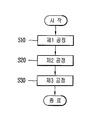
도 4는 본 발명의 일실시예에 따른 표시장치용 가요성 기판의 제조 공정을 나타내는 흐름도이고, 도 5a 내지 도 5b는 본 발명의 일실시예에 따른 표시장치용 가요성 기판의 제조 공정을 나타내는 단면도이다.4 is a flowchart illustrating a manufacturing process of a flexible substrate for a display device according to an embodiment of the present invention, and FIGS. 5A to 5B illustrate a manufacturing process of a flexible substrate for a display device according to an embodiment of the present invention. It is a cross section.
도 4를 참조하면, 본 발명의 일실시예에 따른 표시장치용 가요성 기판의 제조 공정은 제1 내지 제3 공정(S10 내지 S30)으로 나누어진다. Referring to FIG. 4, the manufacturing process of the flexible substrate for the display device according to the exemplary embodiment of the present invention is divided into first to third processes S10 to S30.
도 5a를 참조하면, 먼저 제1 공정((S10)은 가요성 기판(140)에 표시장치의 제조 공정을 지탱하는 지지력을 부여해주기 위해 비가요성 기판(100)에 점착층(120)을 부착하여 공정 장비쪽으로 반송하는 공정이다. Referring to FIG. 5A, first, in operation S10, an
이때, 비가요성 기판(100)은 열에 의해 기판이 변형되는 것을 최소화 하기 위해 세라믹(ceramic), 스테인레스 스틸(SUS: stainless steel), 구리(copper), 티타늄(titanium) 또는 양극산화(anodizing) 처리된 알루미늄(Al) 등이 사용될 수 있으며, 비가요성 기판(100)에 사용될 물질의 탄성계수는 70GPa 이상인 것을 사용한다.In this case, the
여기서, 점착층(120)은 유기 물질을 스핀 코팅(spin coating) 또는 와이어 본딩 코팅(wire bonding coating) 등과 같은 방법을 사용하여 형성할 수 있으며, 또한, 점착층(120)의 점도는 대면적 기판에 코팅 가능한 정도의 점도일 수 있다. Here, the
도 5b를 참조하면, 비가요성 기판(100)의 점착층(120) 상에 가요성 기판(140)을 부착한다. 이때, 가요성 기판(140)은 스테인레스 스틸(SUS: stainless steel) 등을 포함하는 메탈 호일(metal foil)로 이루어질 수 있다.Referring to FIG. 5B, the
이어서, 제2 공정(S20)은 가요성 기판(140) 상에 표시장치의 소자 및 신호 배선을 형성하는 등 일반적인 표시장치를 제조하는 공정과 동일한 공정이다. 이러한 표시장치의 제조 공정을 통해 액정표시장치 또는 유기발광표시장치 등 다양한 표시장치의 제조 공정이 진행될 수 있다. Subsequently, the second process S20 is the same as the process of manufacturing a general display device, such as forming elements and signal wirings of the display device on the
도 3을 참조하면, 비가요성 기판(100)의 상면에는 유기막(160)을 형성한다. 이때, 유기막(160)은 포토 아크릴 또는 폴리 이미드와 같은 유기 물질로 형성할 수 있다. Referring to FIG. 3, an
마지막으로, 제3 공정(S30)은 제2 공정(S20) 후 가요성 기판(140)을 지지해 주는 역할을 하는 비가요성 기판(100)을 점착층(120)으로부터 박리하는 공정이다. 또한, 가요성 기판(140)과 비가요성 기판(100) 사이에 위치하는 점착층(120)도 제2 공정(S20) 후에 박리할 수 도 있다.Finally, the third step S30 is a step of peeling the
본 발명의 일실시예에서는 도 3에서와 같이 가요성 기판을 형성함으로써 가요성 기판의 제조 공정을 단순화하여 제조 비용을 절감할 수 있다.In one embodiment of the present invention by forming a flexible substrate as shown in Figure 3 it is possible to simplify the manufacturing process of the flexible substrate to reduce the manufacturing cost.
또한, 가요성 기판 제조시 도 2에서와 같이 박막트랜지스터(TFT) 형성 후, 기판(20)의 배면을 식각하는 공정을 생략할 수 있으므로, 기판의 복원력을 향상시킬 수 있으며 아울러 기판(20)의 배면의 두께를 균일하게 할 수 있다.In addition, since the process of etching the back surface of the
상기한 설명에 많은 사항이 구체적으로 기재되어 있으나 이것은 발명의 범위를 한정하는 것이라기보다 바람직한 실시예의 예시로서 해석되어야 한다. 따라서, 발명은 설명된 실시예에 의하여 정할 것이 아니고 특허청구범위와 특허청구범위에 균등한 것에 의하여 정하여져야 한다.Many details are set forth in the foregoing description but should be construed as illustrative of preferred embodiments rather than to limit the scope of the invention. Therefore, the invention should not be defined by the described embodiments, but should be defined by the claims and their equivalents.
100: 비가요성 기판 120: 점착층
140: 가요성 기판 160: 유기막100: non-flexible substrate 120: adhesive layer
140: flexible substrate 160: organic film
Claims (10)
비가요성 기판 상에 형성된 점착층;
상기 점착층 상에 형성된 가요성 기판; 및
상기 가요성 기판의 전면에 형성된 유기막을 포함하는 것을 특징으로 하는 표시장치용 가요성 기판.Inflexible substrates;
An adhesive layer formed on the non-flexible substrate;
A flexible substrate formed on the adhesive layer; And
And an organic layer formed on an entire surface of the flexible substrate.
상기 비가요성 기판은 세라믹(ceramic), 스테인레스 스틸(stainless steel), 구리(copper), 티타늄(titanium) 또는 양극산화(anodizing) 처리된 알루미늄(Al) 중에서 선택된 어느 하나로 형성된 것을 특징으로 하는 표시장치용 가요성 기판.The method of claim 1,
The non-flexible substrate is formed of any one selected from ceramic, stainless steel, copper, titanium, or anodized aluminum. Flexible substrate.
상기 비가요성 기판의 탄성계수는 70GPa 이상인 것을 특징으로 하는 표시장치용 가요성 기판.The method of claim 1,
And a modulus of elasticity of the non-flexible substrate is 70 GPa or more.
상기 가요성 기판은 메탈 호일(metal foil)로 형성된 것을 특징으로 하는 표시장치용 가요성 기판.The method of claim 1,
The flexible substrate is a flexible substrate for a display device, characterized in that formed of a metal foil (metal foil).
상기 유기막은 포토 아크릴 또는 폴리 이미드를 포함하는 유기 물질로 형성된 것을 특징으로 하는 표시장치용 가요성 기판.The method of claim 1,
The organic layer is a flexible substrate for a display device, characterized in that formed of an organic material containing a photo acrylic or polyimide.
상기 점착층 상에 가요성 기판을 형성하는 단계; 및
상기 가요성 기판 전면에 유기막을 형성하는 단계를 포함하는 것을 특징으로 하는 표시장치용 가요성 기판의 제조방법.Forming an adhesive layer on the non-flexible substrate;
Forming a flexible substrate on the adhesive layer; And
And forming an organic layer on the entire surface of the flexible substrate.
상기 비가요성 기판은 세라믹(ceramic), 스테인레스 스틸(stainless steel), 구리(copper), 티타늄(titanium) 또는 양극산화(anodizing) 처리된 알루미늄(Al) 중에서 선택된 어느 하나로 형성되는 것을 특징으로 하는 표시장치용 가요성 기판의 제조방법.The method of claim 6,
The non-flexible substrate is formed of any one selected from ceramic, stainless steel, copper, titanium, or anodized aluminum. Method for producing a flexible substrate for use.
상기 비가요성 기판의 탄성계수는 70GPa 이상인 것을 특징으로 하는 표시장치용 가요성 기판의 제조방법.The method of claim 6,
The method of manufacturing a flexible substrate for a display device, characterized in that the elastic modulus of the non-flexible substrate is 70GPa or more.
상기 가요성 기판은 메탈 호일(metal foil)로 형성되는 것을 특징으로 하는 표시장치용 가요성 기판의 제조방법.The method of claim 6,
The flexible substrate is a method of manufacturing a flexible substrate for a display device, characterized in that formed of a metal foil (metal foil).
상기 유기막은 포토 아크릴 또는 폴리 이미드를 포함하는 유기 물질로 형성되는 것을 특징으로 하는 표시장치용 가요성 기판의 제조방법.The method of claim 6,
The organic layer is a method of manufacturing a flexible substrate for a display device, characterized in that formed of an organic material containing a photo acrylic or polyimide.
Priority Applications (1)
| Application Number | Priority Date | Filing Date | Title |
|---|---|---|---|
| KR1020100103715A KR20120042181A (en) | 2010-10-22 | 2010-10-22 | Flexible substrate for display device and manufacturing method comprising the same |
Applications Claiming Priority (1)
| Application Number | Priority Date | Filing Date | Title |
|---|---|---|---|
| KR1020100103715A KR20120042181A (en) | 2010-10-22 | 2010-10-22 | Flexible substrate for display device and manufacturing method comprising the same |
Publications (1)
| Publication Number | Publication Date |
|---|---|
| KR20120042181A true KR20120042181A (en) | 2012-05-03 |
Family
ID=46262990
Family Applications (1)
| Application Number | Title | Priority Date | Filing Date |
|---|---|---|---|
| KR1020100103715A KR20120042181A (en) | 2010-10-22 | 2010-10-22 | Flexible substrate for display device and manufacturing method comprising the same |
Country Status (1)
| Country | Link |
|---|---|
| KR (1) | KR20120042181A (en) |
Cited By (2)
| Publication number | Priority date | Publication date | Assignee | Title |
|---|---|---|---|---|
| WO2015099238A1 (en) * | 2013-12-27 | 2015-07-02 | 코오롱글로텍주식회사 | Flexible fabric substrate and method for manufacturing same |
| KR20160128649A (en) * | 2015-04-29 | 2016-11-08 | 엘지디스플레이 주식회사 | Flexible Substrate, Flexible Display Device Using the Same and Method for Manufacturing the Same |
-
2010
- 2010-10-22 KR KR1020100103715A patent/KR20120042181A/en not_active Application Discontinuation
Cited By (2)
| Publication number | Priority date | Publication date | Assignee | Title |
|---|---|---|---|---|
| WO2015099238A1 (en) * | 2013-12-27 | 2015-07-02 | 코오롱글로텍주식회사 | Flexible fabric substrate and method for manufacturing same |
| KR20160128649A (en) * | 2015-04-29 | 2016-11-08 | 엘지디스플레이 주식회사 | Flexible Substrate, Flexible Display Device Using the Same and Method for Manufacturing the Same |
Similar Documents
| Publication | Publication Date | Title |
|---|---|---|
| CN108257509B (en) | Flexible display device | |
| US20210336161A1 (en) | Flexible oled module stacked structure and manufacturing method thereof | |
| KR20200063801A (en) | Flexible display apparatus | |
| US20110122559A1 (en) | Flexible display device and fabrication method thereof | |
| JP6845351B2 (en) | Manufacturing method of flexible array substrate | |
| US20130135829A1 (en) | Display module | |
| JP6742523B2 (en) | Method for manufacturing flexible array substrate | |
| CN103810945A (en) | Display device having bent non-display area for reduced bezel width | |
| US20180267765A1 (en) | Jointed display screen | |
| KR20150063876A (en) | Display device | |
| KR20110080559A (en) | Electronic paper panel, manufacturing method thereof and electronic paper display device having same | |
| JP2019066849A (en) | Flexible display device and method of manufacturing the same | |
| TWI665648B (en) | Supporting frame and display device including the same | |
| TW201928462A (en) | Back cover and display including the same | |
| US20110157536A1 (en) | Electric circuit structure | |
| KR101844529B1 (en) | Display apparatus | |
| KR20100038921A (en) | Backlight unit and liquid crystal display device having the same | |
| KR102213438B1 (en) | Method of fabricating the flexible display device | |
| KR20120042181A (en) | Flexible substrate for display device and manufacturing method comprising the same | |
| US20240324276A1 (en) | Display apparatus and method of fabricating display apparatus | |
| US9036357B2 (en) | Display device and method of manufacturing the same | |
| US20220317355A1 (en) | Display apparatus | |
| KR20120116813A (en) | Flexible display device and method of manufacturing the same | |
| US12178030B2 (en) | Display device and display apparatus | |
| KR20160033817A (en) | Display device |
Legal Events
| Date | Code | Title | Description |
|---|---|---|---|
| PA0109 | Patent application |
Patent event code: PA01091R01D Comment text: Patent Application Patent event date: 20101022 |
|
| PG1501 | Laying open of application | ||
| PC1203 | Withdrawal of no request for examination | ||
| WITN | Application deemed withdrawn, e.g. because no request for examination was filed or no examination fee was paid |