KR20110082027A - Data paths for multi-level cell memory, how to store and how to use memory arrays - Google Patents
Data paths for multi-level cell memory, how to store and how to use memory arrays Download PDFInfo
- Publication number
- KR20110082027A KR20110082027A KR1020117009985A KR20117009985A KR20110082027A KR 20110082027 A KR20110082027 A KR 20110082027A KR 1020117009985 A KR1020117009985 A KR 1020117009985A KR 20117009985 A KR20117009985 A KR 20117009985A KR 20110082027 A KR20110082027 A KR 20110082027A
- Authority
- KR
- South Korea
- Prior art keywords
- data
- memory
- bits
- bit
- memory cells
- Prior art date
- Legal status (The legal status is an assumption and is not a legal conclusion. Google has not performed a legal analysis and makes no representation as to the accuracy of the status listed.)
- Granted
Links
- 238000003491 array Methods 0.000 title description 2
- 238000013507 mapping Methods 0.000 claims abstract description 54
- 238000000034 method Methods 0.000 claims abstract description 39
- 238000006243 chemical reaction Methods 0.000 claims description 40
- 238000013500 data storage Methods 0.000 claims 3
- 238000007737 ion beam deposition Methods 0.000 description 24
- 238000010586 diagram Methods 0.000 description 6
- 238000013459 approach Methods 0.000 description 4
- 238000013461 design Methods 0.000 description 4
- 239000004065 semiconductor Substances 0.000 description 3
- 238000004519 manufacturing process Methods 0.000 description 2
- 238000012986 modification Methods 0.000 description 2
- 230000004048 modification Effects 0.000 description 2
- 238000013519 translation Methods 0.000 description 2
- 230000008878 coupling Effects 0.000 description 1
- 238000010168 coupling process Methods 0.000 description 1
- 238000005859 coupling reaction Methods 0.000 description 1
- 230000002427 irreversible effect Effects 0.000 description 1
- 230000002250 progressing effect Effects 0.000 description 1
- 230000004044 response Effects 0.000 description 1
Images


Classifications
-
- G—PHYSICS
- G11—INFORMATION STORAGE
- G11C—STATIC STORES
- G11C16/00—Erasable programmable read-only memories
- G11C16/02—Erasable programmable read-only memories electrically programmable
- G11C16/06—Auxiliary circuits, e.g. for writing into memory
- G11C16/10—Programming or data input circuits
-
- G—PHYSICS
- G11—INFORMATION STORAGE
- G11C—STATIC STORES
- G11C11/00—Digital stores characterised by the use of particular electric or magnetic storage elements; Storage elements therefor
- G11C11/56—Digital stores characterised by the use of particular electric or magnetic storage elements; Storage elements therefor using storage elements with more than two stable states represented by steps, e.g. of voltage, current, phase, frequency
- G11C11/5621—Digital stores characterised by the use of particular electric or magnetic storage elements; Storage elements therefor using storage elements with more than two stable states represented by steps, e.g. of voltage, current, phase, frequency using charge storage in a floating gate
- G11C11/5628—Programming or writing circuits; Data input circuits
-
- G—PHYSICS
- G11—INFORMATION STORAGE
- G11C—STATIC STORES
- G11C11/00—Digital stores characterised by the use of particular electric or magnetic storage elements; Storage elements therefor
- G11C11/56—Digital stores characterised by the use of particular electric or magnetic storage elements; Storage elements therefor using storage elements with more than two stable states represented by steps, e.g. of voltage, current, phase, frequency
- G11C11/5621—Digital stores characterised by the use of particular electric or magnetic storage elements; Storage elements therefor using storage elements with more than two stable states represented by steps, e.g. of voltage, current, phase, frequency using charge storage in a floating gate
- G11C11/5642—Sensing or reading circuits; Data output circuits
-
- G—PHYSICS
- G11—INFORMATION STORAGE
- G11C—STATIC STORES
- G11C16/00—Erasable programmable read-only memories
- G11C16/02—Erasable programmable read-only memories electrically programmable
- G11C16/04—Erasable programmable read-only memories electrically programmable using variable threshold transistors, e.g. FAMOS
-
- G—PHYSICS
- G11—INFORMATION STORAGE
- G11C—STATIC STORES
- G11C16/00—Erasable programmable read-only memories
- G11C16/02—Erasable programmable read-only memories electrically programmable
- G11C16/06—Auxiliary circuits, e.g. for writing into memory
-
- G—PHYSICS
- G11—INFORMATION STORAGE
- G11C—STATIC STORES
- G11C2211/00—Indexing scheme relating to digital stores characterized by the use of particular electric or magnetic storage elements; Storage elements therefor
- G11C2211/56—Indexing scheme relating to G11C11/56 and sub-groups for features not covered by these groups
- G11C2211/564—Miscellaneous aspects
- G11C2211/5641—Multilevel memory having cells with different number of storage levels
Landscapes
- Engineering & Computer Science (AREA)
- Computer Hardware Design (AREA)
- Microelectronics & Electronic Packaging (AREA)
- Read Only Memory (AREA)
- Dram (AREA)
- Semiconductor Memories (AREA)
- Static Random-Access Memory (AREA)
Abstract
메모리 셀당 복수의 비트들의 저장을 제공하도록 멀티-레벨 메모리 셀들을 이용한 메모리용 데이터 경로를 포함하는, 메모리, 데이터 경로, 저장하는 방법, 및 활용하는 방법이 개시되어 있다. 그러한 데이터 경로의 하나는, 비트 맵핑 회로 및 데이터 변환기 회로를 포함한다. 이러한 비트 맵핑 회로는 원래의 데이터의 비트들을 중간 배치의 비트들에 맵핑시키도록 구성될 수 있으며, 이러한 데이터 변환기 회로는 중간 배치의 비트들을 수신하여, 메모리 셀 어레이의 메모리 셀들에 의해 저장되도록 중간 배치의 비트들을 메모리 상태에 대응하는 중간 데이터로 변환시키도록 구성될 수 있다.A memory, a data path, a method of storing, and a method of utilizing are disclosed, including a data path for a memory using multi-level memory cells to provide storage of a plurality of bits per memory cell. One such data path includes a bit mapping circuit and a data converter circuit. This bit mapping circuit can be configured to map the bits of the original data to the bits of the intermediate batch, wherein the data converter circuit receives the bits of the intermediate batch and is arranged to be stored by the memory cells of the memory cell array. Can be configured to convert the bits of P into intermediate data corresponding to the memory state.
Description
본 발명의 실시예들은 일반적으로 반도체 메모리에 관한 것으로서, 특히, 예시된 실시예들 중 하나 이상에 있어서, 메모리 셀 당 하나 초과의 이진 디지트의 디지털 정보를 저장하는 데이터 경로를 갖는 반도체 메모리에 관한 것이다.Embodiments of the present invention generally relate to semiconductor memory, and in particular, to one or more of the illustrated embodiments, to a semiconductor memory having a data path for storing more than one binary digit of digital information per memory cell. .
메모리 소자와 같은 반도체 메모리 시스템의 각각의 메모리 셀은 전통적으로 하나의 이진 디지트(비트)의 디지털 정보를 저장하기 위하여 사용되어 왔다. 많은 량의 디지털 정보를 저장하기 위하여는, 큰 어레이의 메모리 셀들이 사용된다. 셀 당 하나의 비트의 전통적인 접근법에 있어서의 하나의 도전은, 메모리 시스템의 전체 크기를 크게 증가시키지 않고 메모리의 용량을 증대시키기 위하여 메모리 어레이의 크기를 지속적으로 줄이는 것이다. 어레이의 크기를 줄이는 일례의 접근법은, 더 적은 면적을 점유하고, 메모리 셀 밀도와 용량을 증가시키기 위하여 메모리 셀 간의 거리를 줄인 메모리 셀을 설계하는 것이었다. 그러나, 메모리 셀들의 피쳐 크기가 더 작아짐에 따라서, 메모리 제조의 복잡도는 증가하여, 제조 비용의 증가를 가져온다.Each memory cell of a semiconductor memory system, such as a memory device, has traditionally been used to store digital information of one binary digit (bit). To store large amounts of digital information, large arrays of memory cells are used. One challenge in the traditional approach of one bit per cell is to continuously reduce the size of the memory array in order to increase the capacity of the memory without significantly increasing the overall size of the memory system. One example approach to reducing the size of an array has been to design memory cells that occupy less area and reduce the distance between memory cells to increase memory cell density and capacity. However, as the feature size of the memory cells becomes smaller, the complexity of memory fabrication increases, resulting in an increase in fabrication cost.
메모리 용량을 증가시키는 비교적 최근의 접근법은, 다수의 비트의 디지털 정보를 각각의 메모리 셀에 저장하기 위한 지원 회로와 메모리 셀들을 설계하는 것이었다. 예를 들어, 전통적인 경우와 같이, 1 비트의 디지털 정보를 저장하는 것이 아니라, 메모리 셀에 2 비트의 디지털 정보가 저장된다. 2 비트의 디지털 정보의 저장은 4 개의 구분된 메모리 상태를 정확하게 저장, 판독, 및 기입할 수 있는 판독/기입 회로와 메모리 셀들을 가짐으로써 성취된다. 4 개의 메모리 상태 각각은 2 비트의 정보의 상이한 조합, 즉, 00, 01, 10, 및 11을 나타낸다. 이와 대조하여, 전통적인 셀당 1 비트의 접근법은, 각각 구분된 메모리 상태가 0 또는 1을 나타내는, 2 개의 구분된 메모리 상태를 정확하게 저장, 판독, 기입할 수 있는 판독/기입 회로 및 메모리 셀들을 필요로 한다. 2 이상의 메모리 상태를 저장하기 위한 메모리 셀들의 사용은, 예를 들어, 휘발성(예컨대, DRAM) 및 비휘발성(예컨대, 플래시 메모리) 양측 모두에 있어서 상이한 유형의 메모리에 대하여 적용가능할 수 있다.A relatively recent approach to increasing memory capacity has been to design support circuits and memory cells for storing multiple bits of digital information in each memory cell. For example, as in the traditional case, rather than storing one bit of digital information, two bits of digital information are stored in a memory cell. The storage of two bits of digital information is achieved by having read / write circuits and memory cells capable of accurately storing, reading, and writing four separate memory states. Each of the four memory states represents a different combination of two bits of information, namely 00, 01, 10, and 11. In contrast, the traditional one bit per cell approach requires read / write circuits and memory cells capable of accurately storing, reading, and writing two separate memory states, each representing a separate memory state of zero or one. do. The use of memory cells to store two or more memory states may be applicable for different types of memory, for example, in both volatile (eg DRAM) and nonvolatile (eg flash memory).
2 이상의 메모리 상태를 저장하기 위하여 메모리 셀들을 사용하는 것의 현재의 추세에 따라서 앞으로 진행하여, 1 비트의 디지털 정보를 저장하기 위하여 2 개의 상이한 메모리 상태를 사용하는 것으로 시작하여, 2 비트의 디지털 정보를 저장하기 위하여 4 개의 상이한 메모리 상태를 사용하는 것으로 진보한다면, 8 개의 상이한 메모리 상태에 의해 3 비트의 디지털 정보가 저장될 수 있으며, 16 개의 상이한 메모리 상태를 사용하여 4 비트의 디지털 정보가 저장될 수 있다. 본 예에서 나타낸 바와 같이, 메모리 셀당 메모리 상태의 수는 2의 거듭제곱이며, 그 결과의 셀당 저장되는 비트의 수는 메모리 상태의 수의 기수 2의 로그함수이다.Moving forward in accordance with the current trend of using memory cells to store two or more memory states, beginning with using two different memory states to store one bit of digital information, Advancing to using four different memory states to store, three bits of digital information can be stored by eight different memory states, and four bits of digital information can be stored using sixteen different memory states. have. As shown in this example, the number of memory states per memory cell is a power of two, and the resulting number of bits stored per cell is a logarithm of the base two of the number of memory states.
이러한 추세에 따라서 메모리 시스템을 설계하는 시도는, 예를 들어, 이전의 반복보다 2 배의 메모리 상태를 확실하고 정확하게 저장, 판독, 및 기입하여야 하는 애로 사항이 있다. 2 개의 메모리 상태를 저장, 판독, 기입하는 것으로부터 4 개의 메모리 상태를 저장, 판독, 기입하는 것으로 진보하는 것은, 결국 극복된 애로사항이 있다는 것이다. 그러나, 4 개의 메모리 상태를 사용하는 것에서 8 개의 메모리 상태를 사용하는 것으로 진보하는 것은, 2 개의 메모리 상태에서 4 개의 메모리 상태로의 종래의 진보에서 있었던 것보다 현재의 기술 수준으로서는 더욱 더 어려운 도전이다. 애로 사항이 해소 불가능한 것이 아니며, 종국적으로는 극복될 것이지만, 예를 들어, 2의 거듭제곱 수의 메모리 상태를 저장하는 것에 한하지 않고 셀당 1 비트 이상의 저장 밀도를 제공하도록 다수의 메모리 상태를 저장하기 위한 메모리 셀들을 활용하는 메모리 시스템이 요구된다고 하겠다.Attempts to design a memory system in accordance with this trend, for example, have the challenge of storing, reading, and writing twice as many memory states as previous repetitions. Advancing from storing, reading, and writing two memory states to storing, reading, and writing four memory states is, in the end, a challenge that has been overcome. However, progressing from using four memory states to using eight memory states is a more difficult challenge at the current state of the art than was possible with the conventional advancement from two memory states to four memory states. . The bottleneck is not irreversible and will eventually be overcome, but storing multiple memory states to provide a storage density of more than 1 bit per cell, for example, not only storing memory states of powers of two. There is a need for a memory system that utilizes memory cells.
도 1은 본 발명의 일 실시예에 따른 데이터 경로의 블록도이다.
도 2a는 본 발명의 일 실시예에 따른 비트 맵핑 및 데이터 변환 회로(130)를 갖는 데이터 경로의 블록도이다.
도 2b는 2의 거듭제곱이 아닌 메모리 상태를 갖는 메모리 어레이의 멀티-레벨 메모리 셀의 쌍을 사용하는 것에 관한 결과적인 비트/셀 저장 밀도의 표이다.
도 3은 본 발명의 일 실시예에 따라서 6개의 메모리 상태를 갖는 멀티-레벨 메모리 셀의 쌍을 사용하여 이진 사용자 데이터를 저장하기 위한 진리표이다.
도 4는 본 발명의 일 실시예에 따라서 3개의 메모리 상태를 갖는 멀티-레벨 메모리 셀의 쌍을 사용하여 이진 사용자 데이터를 저장하기 위한 진리표이다.
도 5는 6개의 메모리 상태를 갖는 멀티-레벨 메모리 셀의 쌍을 사용하여 데이터를 저장하기 위한 본 발명의 일 실시예에 따른 데이터 경로의 블록도이다.
도 6은 3개의 메모리 상태를 갖는 멀티-레벨 셀의 쌍을 이용하여 데이터를 저장하기 위한 본 발명의 일 실시예에 따른 데이터 경로의 블록도이다.
도 7은 4개의 메모리 상태를 갖는 멀티-레벨 셀의 쌍을 이용하여 데이터를 저장하기 위한 본 발명의 일 실시예에 따른 데이터 경로의 블록도이다.
도 8은 본 발명의 일 실시예에 따른 데이터 경로를 갖는 메모리 시스템의 블록도이다.1 is a block diagram of a data path in accordance with one embodiment of the present invention.
2A is a block diagram of a data path having bit mapping and
FIG. 2B is a table of the resulting bit / cell storage densities for using a pair of multi-level memory cells of a memory array having a memory state other than power of two.
3 is a truth table for storing binary user data using a pair of multi-level memory cells having six memory states in accordance with one embodiment of the present invention.
4 is a truth table for storing binary user data using a pair of multi-level memory cells having three memory states in accordance with one embodiment of the present invention.
5 is a block diagram of a data path in accordance with one embodiment of the present invention for storing data using a pair of multi-level memory cells having six memory states.
6 is a block diagram of a data path in accordance with an embodiment of the present invention for storing data using a pair of multi-level cells having three memory states.
7 is a block diagram of a data path in accordance with one embodiment of the present invention for storing data using a pair of multi-level cells having four memory states.
8 is a block diagram of a memory system having a data path according to an embodiment of the present invention.
본 발명의 실시예에 대한 충분한 이해를 위하여 상세한 설명을 이하에 명기한다. 그러나, 당업자라면, 본 발명의 실시예는 이러한 특정 세부사항 없이도 실시될 수 있다는 것을 이해할 수 있을 것이다. 또한, 본 명세서에 기술되는 본 발명의 특정 실시예들은 일례로서 제공하는 것으로서, 이러한 특정 실시예에 본 발명의 범주를 제한하도록 사용되어서는 아니된다. 다른 경우에 있어서, 공지의 회로, 제어 신호, 타이밍 프로토콜, 및 소프트웨어 동작들은 불필요하게 본 발명을 모호하게 만들지 않도록 상세하게 나타내지 않았다.Detailed descriptions are provided below for a sufficient understanding of the embodiments of the present invention. However, it will be apparent to one skilled in the art that embodiments of the present invention may be practiced without these specific details. In addition, certain embodiments of the invention described herein are provided as examples and should not be used to limit the scope of the invention to such specific embodiments. In other instances, well-known circuits, control signals, timing protocols, and software operations have not been shown in detail in order not to unnecessarily obscure the present invention.
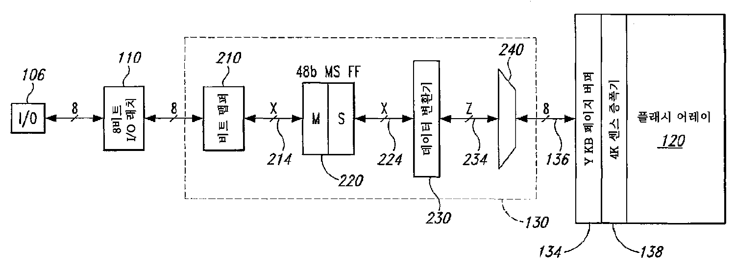
도 1은 본 발명의 일 실시예에 따른 데이터 경로(100)를 나타낸다. 데이터 경로(100)는 데이터 기입을 위하여 단자(106)와 같은 I/O(Input/Output) 노드에 인가되는 데이터들을 플래시 메모리 어레이(120)에 결합시키며, 판독 데이터 제공을 위하여 플래시 메모리 어레이(120)로부터의 데이터를 I/O 단자(106)에 결합시킨다. 메모리 어레이(120)는 P개의 상이한 메모리 셀 상태를 저장하는 멀티-레벨 메모리 셀을 포함하며, 여기서, P는 2의 거듭제곱이 아닌 수일 수 있다. 데이터 경로(100)는 이진 디지트(즉, "비트")의 정보를 래치하기 위하여 I/O 단자(106)에 결합되는 I/O 래치(110)를 포함한다. 도 1에 나타낸 실시예에 있어서, I/O 래치(106)는 8 비트 폭이며, I/O 단자(106)은 8 개의 단자를 나타낸다. 본 발명의 일 실시예에 따른 비트 맵핑 및 데이터 변환 회로(130)는 래치(110)에 결합된다. 비트 맵핑 및 데이터 변환 회로(130)는, 이하에서 상세하게 후술하지만, 메모리 어레이(120)가 셀당 N개의 비트를 저장할 수 있도록 구성되는 것으로서, 여기서, N은 정수가 아닌 수일 수 있다. 비트 맵핑 및 데이터 변환 회로(130)는 데이터 버스(136)(8비트 폭으로서 도 1에 도시됨)를 통해 페이지 버퍼(134)에 결합되며, 이어서, 센스 증폭기(138) 및 플래시 메모리 어레이(120)에 결합된다. 데이터 경로(100)는 I/O 래치(110)와 버퍼(134) 사이에 결합되는 비트 맵핑 및 데이터 변환 회로를 포함하는 것을 제외하고는 종래의 데이터 경로와 유사하다. 도 1에 도시된 실시예에 있어서, 페이지 버퍼는 4 kBits (4,096 비트)를 저장할 수 있으며, 센스 증폭기(138)는 4 k 센스 증폭기를 포함한다. 데이터 경로(100)에 제공되는 특정의 비트-크기는 일례로서 제공되는 것이며, 본 발명의 다른 실시예들에서는 상이한 비트-크기를 갖는 소자들을 포함한다.1 illustrates a
도 2a는 본 발명의 일 실시예에 따른 비트 맵핑 및 데이터 변환 회로(130)를 갖는 데이터 경로(100)를 나타낸다. 비트 맵핑 및 데이터 변환 회로(130)는 입출력(I/O) 래치(110)로부터 레지스터(220)에 데이터의 비트들을 맵핑시키거나, 그 역으로 맵핑시키기 위하여 버스(214)를 통해 레지스터(220)에 결합되는 비트 맵핑 회로(210)를 포함한다. 버스(224)를 통해 레지스터(220)에 결합되는 데이터 변환기(230)는 데이터 비트들을, 멀티플렉서(240)를 통해 페이지 버퍼(134)에 기입되도록 버스(234) 상으로 제공되는 중간 이진 데이터(IBD: Intermediate Binary Data)로 변환한다. 데이터 변환기(230)는 또한 페이지 버퍼(134)로부터 판독된 IBD를 레지스터(220)에 저장되는 데이터로 변환하여, 비트 맵핑 회로(210)를 통해 래치(110)에 제공되도록 한다. 멀티플렉서(240)는 상이한 비트 폭을 가질 수 있는 버스(234)와 버스(136)와의 사이에 IBD를 라우팅한다. 도 2a에 도시된 본 발명의 실시예에 있어서, 입출력 래치는 8 비트 폭이며, 버스(136) 또한 8 비트 폭이다. 그러나, 다른 실시예로서, 버스들의 비트 폭은 상이할 수 있다.2A illustrates a
동작에 있어서, 비트 맵핑 및 데이터 변환 회로(130)는 이진 사용자 데이터를 IBD로 변환하고, 또 그 역으로 변환하도록 구성될 수 있다. IBD는 메모리 어레이(120)의 메모리 셀에 메모리 셀 상태로서 저장될 수 있는 중간 이진 데이터이다. 전술한 바와 같이, 비트 맵핑 및 데이터 변환 회로(130)는 정수가 아닌 수의 셀당 비트(bits per cell)들을 효과적으로 저장하기 위하여 2의 거듭제곱이 아닌 메모리 상태를 저장할 수 있는 멀티-레벨 메모리 셀들의 그룹을 이용하여 이진 사용자 데이터가 저장될 수 있도록 사용될 수 있다. 정수가 아닌 수의 셀당 비트들을 제공하기 위하여 2의 거듭제곱이 아닌 상태들을 갖는 메모리 셀들의 그룹을 이용하여 이진 사용자 데이터를 저장하는 것은, 종래의 바이트 및 워드 길이로 이진 데이터를 기입 및 판독할 수 있는 사용자에게 분명한 것이다.In operation, bit mapping and
비트 맵핑 및 데이터 변환 회로(130)의 상이한 구성의 예들이 도 2b의 표(250)에 도시되어 있으며, 이는 비한정적인 예로서 제공되는 것이다. 표(250)에 도시된 일례의 구성들은, 2개의 메모리 셀들의 그룹을 활용하여 생긴 결과이고, 메모리 셀들에 의해 어레이에 저장가능한 대응하는 수의 메모리 상태에 대하여 각각의 셀당 비트의 저장 밀도를 제공한다. 예를 들어, 2개의 메모리 셀들의 그룹을 가정하면, 비트 맵핑 및 데이터 변환 회로(130)는 6개의 저장가능한 메모리 상태를 갖는 메모리 셀들로 사용되는 경우, 2.5 비트/셀의 저장 밀도를 제공하도록 구성될 수 있다. 또 다른 구성에 있어서, 비트 맵핑 및 데이터 변환 회로(130)는 4개의 저장가능한 메모리 상태를 갖는 메모리 셀들로 사용되는 경우, 2 비트/셀의 저장 밀도를 제공할 수 있다. 이하의 예에서 나타내는 바와 같이, 비트 맵핑 및 데이터 변환 회로(130)는 또한 통상의 셀당 비트의 저장 밀도를 제공하기 위하여 통상의 2의 거듭제곱의 저장가능한 메모리 상태를 갖는 메모리 셀들로 사용될 수도 있다.Examples of different configurations of the bit mapping and
도 3은 본 발명의 일 실시예에 따라서 각각 6개의 메모리 상태를 갖는, 2개의 메모리 셀들의 그룹에 의해 저장되는 IBD와 이진 사용자 데이터와의 사이의 변환을 위한 표(310 및 320)를 나타낸다. 도 2와 표(250)를 참조하여 앞서 설명한 바와 같이, 6개의 저장가능한 메모리 상태(L0-L5)를 가지며, 2개의 메모리 셀(Cell0 및 Cell1)의 그룹을 이용하는 실시예에 있어서, 2.5 비트/셀의 저장 밀도가 성취된다. 표(310)은 이진 사용자 데이터의 5비트 값들에 대한 2개의 메모리 셀의 6개 메모리 상태(L0-L5)의 조합의 할당을 나타낸다. 이하에서 상세하게 설명하는 바와 같이, 사용자의 8 비트 데이터(즉, 1 byte)는 데이터 변환기(230)에 의해 IBD로 변환되는 5 비트의 이진 데이터로 분할된다. 그 후, IBD는 한 쌍의 메모리 셀에 저장된다. 표(320)는 그 쌍의 개별 셀들에 대한 메모리 상태와 IBD 간의 변환을 나타낸다.3 shows tables 310 and 320 for conversion between IBD and binary user data stored by a group of two memory cells, each having six memory states, in accordance with one embodiment of the present invention. As described above with reference to FIG. 2 and table 250, in the embodiment having six storeable memory states L0-L5 and using a group of two memory cells Cell0 and Cell1, 2.5 bits / The storage density of the cell is achieved. Table 310 shows the allocation of a combination of six memory states L0-L5 of two memory cells to 5-bit values of binary user data. As will be described in detail below, the user's 8-bit data (ie, 1 byte) is divided into 5-bit binary data which is converted into IBD by the
예를 들어, 8 비트 이진 사용자 데이터가 01011101(B7:B0)이며, 메모리에 기입되어야 하는 경우, 사용자 데이터는 첫번째 5비트 이진 데이터로 분할되고, 나머지 3 비트는 다른 5 비트 이진 데이터의 일부가 된다. 특정한 예로서, 첫번째 5비트 이진 데이터(B4:B0)는 11101이며, 나머지 3비트 010(B7:B5)는 다른 8비트 이진 사용자 데이터로부터의 5개의 다른 비트과 결합되게 된다. 5비트 이진 데이터 11101(B4:B0)와 표(310)를 참조하면, 이진 데이터는 한 쌍의 멀티레벨 메모리 셀(Cell0 및 Cell1)의 쌍에 의해 각각 저장된 메모리 셀 상태(L0 및L2)의 조합에 대응한다. 이하에서 상세하게 설명하는 바와 같이, 해당 메모리 셀에 의해 저장될 메모리 상태를 결정함에 있어서, 5비트 이진 데이터는 2개의 3비트 IBD로 변환되며, 이어서, 이는 각각 표(320)에 따라서 해당 메모리 셀에 대응하는 메모리 상태로서 저장된다.For example, if 8-bit binary user data is 01011101 (B7: B0) and must be written to memory, the user data is divided into the first 5-bit binary data and the remaining 3 bits become part of the other 5-bit binary data. . As a specific example, the first 5 bit binary data B4: B0 is 11101 and the remaining 3 bits 010 (B7: B5) are combined with 5 different bits from other 8 bit binary user data. Referring to the 5-bit binary data 11101 (B4: B0) and the table 310, the binary data is a combination of memory cell states L0 and L2 respectively stored by a pair of multilevel memory cells Cell0 and Cell1. Corresponds to. As will be described in detail below, in determining the memory state to be stored by the memory cell, 5-bit binary data is converted into two 3-bit IBDs, which are each corresponding to the memory cell in accordance with Table 320, respectively. Is stored as a memory state corresponding to.
메모리로부터 데이터를 판독하는 경우, 한 쌍의 셀이 액세스되어, 6개의 메모리 상태를 갖는 메모리 셀들에 대하여 해당 메모리 상태가 종래와 같이 감지되어, 각각의 메모리 셀에 대하여 대응하는 3비트 IBD를 제공한다. 예를 들어, 메모리 셀(Cell0 및 Cell1)에 의해 각각 저장된 메모리 셀 상태(L0 및 L2)를 판독함으로써, 2개의 메모리 셀이 액세스되고, 메모리 상태(L0 및 L2)는 2개의 3비트 IBD인 111 및 101을 초래한다. 3비트 IBD는 다시 5비트의 이진 데이터로 변환된다. 표(310)에 따르면, 그 결과의 5비트 데이터는 11101이며, 이는 메모리에 데이터를 기입하는 이전의 예에서의 원래의 5비트 이진 데이터이다. 5비트 이진 데이터는 그후 메모리로부터 판독되어 원래의 8비트 이진 사용자 데이터로 분할되는 다른 5비트 이진 데이터와 연결된다.When reading data from the memory, a pair of cells are accessed so that the memory state is conventionally detected for memory cells having six memory states, providing a corresponding 3-bit IBD for each memory cell. . For example, by reading the memory cell states L0 and L2 stored by the memory cells Cell0 and Cell1, respectively, two memory cells are accessed, and the memory states L0 and L2 are 111 which are two 3-bit IBDs. And 101. The 3-bit IBD is converted back into 5-bit binary data. According to table 310, the resulting 5-bit data is 11101, which is the original 5-bit binary data in the previous example of writing data to memory. The 5-bit binary data is then concatenated with other 5-bit binary data that is read from memory and divided into original 8-bit binary user data.
도 4는 본 발명의 일 실시예에 따라서 각각 3개의 메모리 상태를 갖는 2개의 메모리 셀의 그룹들에 의해 저장되는 IBD들과 이진 사용자 데이터와의 사이의 변환을 위한 표(330 및 340)를 나타난다. 도 2 및 표(250)를 참조하여 상기 설명한 바와 같이, 3개의 저장가능한 메모리 상태(L0-L2)를 갖는 메모리 셀들을 활용하고, 2개의 메모리 셀(Cell0 및 Cell1)의 그룹을 사용하는 실시예에 있어서, 1.5 비트/셀의 저장 밀도가 성취된다. 표(330)은 이진 사용자 데이터의 3비트 값들에 대한 2개의 메모리 셀들의 3개의 메모리 상태(L0-L2)의 조합들의 할당을 나타낸다. 이하에서 더 상세하게 설명하는 바와 같이, 사용자의 8비트 데이터는 데이터 변환기(230)에 의해 IBD로 변환되는 3비트 이진 데이터로 분할된다. IBD는 그 후 한 쌍의 메모리 셀에 저장된다. 표(340)는 그 쌍의 개별 셀들의 메모리 상태와 IBD간의 변환을 나타낸다.4 shows tables 330 and 340 for conversion between IBDs and binary user data stored by groups of two memory cells each having three memory states in accordance with one embodiment of the present invention. . As described above with reference to FIG. 2 and table 250, an embodiment utilizes memory cells having three storeable memory states L0-L2 and uses a group of two memory cells Cell0 and Cell1. For a storage density of 1.5 bits / cell is achieved. Table 330 shows the allocation of combinations of three memory states L0-L2 of two memory cells to three bit values of binary user data. As described in more detail below, the user's 8-bit data is divided into 3-bit binary data that is converted into IBD by the
예를 들어, 8비트 이진 사용자 데이터가 01011101(B7:B0)이며, 메모리에 기입되어야 하는 경우, 사용자 데이터는 첫번째 3비트 이진 데이터(B2:B0)와 두번째 3비트 이진 데이터(B5:B3)로 분할되고, 나머지 2비트(B7:B6)는 또 다른 3비트 이진 데이터의 일부가 된다. 특정한 예에 있어서, 첫번째 3비트 이진 데이터는 101이며, 두번째 3비트 이진 데이터는 011이며, 나머지 2비트 01은 다른 8비트 이진 사용자 데이터로부터의 하나의 다른 비트와 결합되게 된다. 2개의 3비트 이진 데이터 101 및 011와 표(330)를 참조하면, 첫번째 이진 데이터 101는 제1 쌍의 멀티-레벨 메모리 셀(Cell0 및 Cell1)에 의해 각각 저장되는 메모리 셀 상태(L1 및 L0)의 조합에 대응한다. 두번째 이진 데이터(011)는 제2 쌍의 멀티-레벨 메모리 셀(Cell0 및 Cell1) 각각에 의해 저장되는 메모리 셀 상태(L1 및 L2)의 조합에 대응한다. 이하에서 더 상세하게 설명하는 하는 바와 같이, 해당 메모리 셀에 의해 저장되어야 하는 메모리 상태를 결정함에 있어서, 3비트 이진 데이터는 2개의 2비트 IBD로 변환되며, 이어서, 각각 해당 메모리 셀에 대응하는 메모리 상태로서 저장된다.For example, if 8-bit binary user data is 01011101 (B7: B0) and must be written to memory, the user data is the first three-bit binary data (B2: B0) and the second three-bit binary data (B5: B3). The remaining two bits (B7: B6) become part of another 3-bit binary data. In a particular example, the first three bits of binary data is 101, the second three bits of binary data is 011, and the remaining two
메모리로부터 데이터를 판독하는 경우, 한 쌍의 셀이 액세스되고, 3개의 메모리 상태를 갖는 메모리 셀들에 대하여 해당 메모리 상태가 종래와 같이 감지되어, 각각의 메모리 셀에 대하여 대응하는 2비트 IBD를 제공한다. 예를 들어, 제1 쌍의 메모리 셀(Cell0 및 Cell1)에 의해 각각 저장되는 메모리 셀 상태(L1 및 L0)에 있어서, 2개의 메모리 셀 상태가 액세스되고, 메모리 상태(L1 및 L0)는 2개의 IBD 10 및 11를 초래한다. 제2 쌍의 멀티레벨 메모리 셀(Cell0 및 Cell1)에 의해 각각 저장되는 메모리 셀 상태(L1 및 L2)에 있어서, 2개의 메모리 셀들이 액세스되고, 메모리 상태(L1 및 L2)는 2개의 IBD 10 및 01를 초래한다. 2비트 IBD는 다시 3비트 이진 데이터로 변환된다. 본 예에 있어서, 표(330)에 따라서, 제1 쌍의 메모리 셀들에 대한 그 결과의 3비트 이진 데이터는 101이며, 제2 쌍의 메모리셀에 에 대한 그 결과의 3비트 이진 데이터는 011이며, 이는 데이터를 메모리에 기입하는 이전의 예로부터의 원래의 3비트 데이터이다. 3비트 이진 데이터는 그 후 메모리로부터 판독되어 원래의 8비트 이진 사용자 데이터로 분할되는 다른 3비트 이진 데이터에 연결된다.When reading data from memory, a pair of cells are accessed, and the memory state is conventionally detected for memory cells having three memory states, providing a corresponding 2-bit IBD for each memory cell. . For example, in the memory cell states L1 and L0 stored by the first pair of memory cells Cell0 and Cell1, respectively, two memory cell states are accessed, and the memory states L1 and L0 are two Results in
도 5는 본 발명의 일 실시예에 따른 비트 맵핑 및 데이터 변환 회로(130)를 갖는 데이터 경로(100)를 나타낸다. 도 5의 데이터 경로(100)는 도 3을 참조하여 상기 설명한 6개의 메모리 상태, 2셀의 예를 구현하기 위하여 사용될 수 있다. 도 5에 도시된 본 발명의 실시예는 비트 맵핑 회로(210)을 통해 48비트 레지스터(220)에 결합되는 8비트 I/O 래치를 포함한다. 48비트 레지스터(220)는 이진 사용자 데이터를 IBD로 변환하는 8개의 데이터 변환기 서브회로(230A-H)에 이진 데이터를 제공하며, IBD는 멀티플렉서(240), 데이터 버스(136), 및 버퍼(134)를 통해 멀티-레벨 메모리 셀 어레이에 기입된다. 센스 증폭기(138)는 페이지 버퍼(134)에 저장되는 멀티-레벨 메모리 셀들과 IBD들에 의해 저장되는 메모리 상태들 사이를 변환한다.5 shows a
동작에 있어서, 래치(110)에 로딩되는 8비트 사용자 데이터가 순차적으로 비트 매핑 회로(210)에 제공되고, 레지스터(220)의 대응하는 위치에 사용자 데이터의 비트들을 맵핑시킨다. 도 5에 도시된 실시예에 있어서, 8비트 사용자 데이터는 적절한 비트 수의 사용자 데이터가 레지스터(220)에 로딩될 때까지 비트 맵핑 회로(210)를 통하여 맵핑된다. 6개의 메모리 상태 및 2개의 셀의 제시된 예에 있어서, 8비트 사용자 데이터는 전술한 바와 같이 5비트 이진 데이터로 분할된다. 레지스터(220)에 저장되는 5비트 이진 데이터는 데이터 변환기 서브회로(230A-H)에 제공되어 3비트 IBD의 쌍들로 변환되며, 이들은 이어서 해당 메모리 셀들에 저장되는 메모리 상태로 변환된다.In operation, 8-bit user data loaded in
예를 들어, 도 3을 참조하여 상기 설명한 예를 사용하면, 8비트 이진 사용자 데이터 01011101(B7:B0)가 래치(110)에 로딩되어, 비트 맵핑 회로(210)를 통해서 레지스터(220)에 맵핑된다. 도 5에 도시된 실시예에 있어서, 비트 11101(B4:B0)는 데이터 변환기 서브회로(230A)에 결합되는 레지스터(220)의 6개 비트 레지스터 위치 중 5개에 맵핑되게 되며, 비트 010(B7:B5)는 데이터 변환기 서브회로(230B)에 결합되는 레지스터(220)의 6개 비트 레지스터 위치 중 3개에 맵핑되게 된다. 8비트 이진 사용자 데이터는 레지스터(220)가 로딩될 때까지 비트 맵핑 회로(210)를 통해 계속 로딩된다. 8비트 사용자 데이터를 5비트 이진 데이터로 분할하는 예에 있어서, 5개의 8비트(바이트)의 사용자 데이터가 그 용량에 다다를 때까지 48비트 레지스터(220)에 로딩될 수 있다. 데이터 변환기 서브회로(230A-H)는 전술한 바와 같이 5비트 이진 데이터를 3비트 IBD로 변환한다. 도 3의 표(310)를 참조하면, 특정 예의 5비트 데이터 11101는 데이터 변환기 서브회로(230A)에 의해 3비트 IBD 111 및 101로 변환되며, 이는 페이지 버퍼(134) 내의 위치(134A 및 134B)에 멀티플렉서(240) 및 데이터 버스(136)를 통해 비트별로 로딩되도록 버스(234) 상으로 제공된다. 레지스터(220)에 저장되는 다른 5비트 이진 데이터는 마찬가지로 데이터 변환기 서브회로(230B-H)에 의해 해당 3비트 IBD의 쌍으로 변환되어, 버스(234), 멀티플렉서(240), 및 데이터 버스(136)를 통해 페이지 버퍼(134)에 로딩된다.For example, using the example described above with reference to FIG. 3, 8-bit binary user data 01011101 (B7: B0) is loaded into the
페이지 버퍼(134)가 IBD로 로딩된 후에, 센스 증폭기(138)는 해당 3비트 IBD를 대응하는 메모리 상태로 변환하고, 이는 해당 멀티-레벨 메모리 셀에 저장된다. IBD를 대응하는 메모리 상태로 변환하기 위한 센스 증폭기는 공지되어 있으며, 센스 증폭기(138)에 대하여 종래의 설계의 센스 증폭기들이 사용될 수 있다. 본 예에 있어서, 3비트 IBD 111는 메모리 상태(L0)에 대응하며(도 3의 표(320)을 참조), 5비트 이진 데이터를 저장하기 위하여 사용되는 한 쌍의 메모리 셀(Cell0 및 Cell1)(도시 생략) 중 제1 메모리 셀(Cell0)에 저장된다. 3비트 IBD 101는 L2에 대응하며, 제2 메모리 셀(Cell1)에 저장된다.After the
멀티-레벨 메모리 셀들로부터 데이터를 판독하는 경우, 데이터를 멀티-레벨 메모리 셀들에 기입하는 과정은 일반적으로 역으로 행해진다. 즉, 멀티-레벨 메모리 셀들에 의해 저장된 메모리 상태들이 센스 증폭기(138)에 의해 감지되어 3비트 IBD들로 변환되어, 페이지 버퍼(134) 내의 해당 위치에 저장된다. 메모리 셀의 쌍들로부터의 IBD들은 해당 데이터 변환기 서브회로에 결합되며, 예를 들어, 위치(134A 및 134B)에 의해 저장된 IBD들은 데이터 버스(136), 멀티플렉서(240),및 버스(234)를 통해 데이터 변환기 서브회로(230A)에 결합된다. 2개의 3비트 IBD들은 데이터 변환기(230)에 의해 해당 5비트 이진 데이터로 변환되어, 레지스터(220) 내의 적절한 비트 위치에 저장된다. 비트 맴핑 회로(210)는 5비트 이진 데이터를 8비트 데이터에 맵핑시켜, 원래의 8비트 이진 사용자 데이터를 재구성한다.When reading data from multi-level memory cells, the process of writing data to multi-level memory cells is generally reversed. That is, the memory states stored by the multi-level memory cells are sensed by the
도 6은 도 4를 참조하여 상기 설명한 3개의 메모리 상태의 2셀의 예를 구현하도록 구성되는 비트 맵핑 및 데이터 변환 회로(130)를 갖는 도 5를 참조하여 상기 설명한 데이터 경로(100)를 나타낸다. 즉, 본 발명의 몇몇 실시예에 있어서, 데이터 경로(100)는, 2의 거듭제곱이 아닌 메모리 상태와 정수가 아닌 수인 비트/셀 저장 밀도를 저장할 수 있는 멀티-레벨 메모리 셀들을 포함하여, 멀티-레벨 메모리 셀을 갖는 메모리에서 상이한 비트/셀 저장 밀도를 구현하도록 구성될 수 있다.FIG. 6 illustrates the
동작에 있어서, 래치(110)에 로딩된 8비트 이진 사용자 데이터는 비트 맵핑 회로(210)에 순차적으로 제공되어, 사용자 데이터의 비트들이 레지스터(220)의 해당 위치들에 맵핑되도록 한다. 도 6에 도시된 실시예에 있어서, 8비트 사용자 데이터는 도 4를 참조하여 상기 설명한 바와 같이 비트 맵핑 회로(210)를 통해 3비트 이진 데이터에 맵핑되어, 레지스터(220)에 저장된다. 레지스터(220)에 저장된 3비트 이진 데이터는 데이터 변환기 서브회로(230A-H)에 제공되어, 2비트 IBD의 쌍들로 변환되며, 이들은 이어서 해당 메모리 셀들에 저장되는 메모리 상태들로 변환된다.In operation, 8-bit binary user data loaded in
예를 들어, 도 4를 참조하여 상기 설명한 예를 이용하여 8비트 이진 사용자 데이터 01011101(B7:B0)가 래치(110)에 로딩되어, 비트 맵핑 회로(210)를 통해 레지스터(220)에 맵핑된다. 도 6에 도시된 실시예에 있어서, 비트 101(첫번째 3비트 B2:B0)이 데이터 변환기 서브회로(230A)에 결합되는 6개의 비트 레지스터 위치들 중 3개에 맵핑되고, 비트 011(두번째 3비트 B5:B3)가 데이터 변환기 서브회로(230B)에 결합되는 6개의 비트 레지스터 위치 중 3개에 맵핑된다. 나머지 비트 01(B7:B6)는 데이터 변환기 서브회로(230C)에 결합되는 6개의 비트 레지스터 위치들 중 2개에 맵핑되어, 래치(110)에 로딩되는 다음의 8비트 사용자 데이터 중 1 비트에 연결되게 된다. 8비트 이진 사용자 데이터는 레지스터(220)가 로딩될 때까지 비트 맵핑 회로(210)를 통해 계속 로딩된다. 8비트 사용자 데이터를 3비트 이진 데이터로 분할하는 예에 있어서, 사용자 데이터 중 3개의 8비트 바이트가 그 용량에 도달할 때까지 48비트 레지스터(220)에 로딩될 수 있다. 데이터 변환기 서브회로(230A-H)는 도 4의 표(340)를 참조하여 상기 설명한 바와 같이 3비트 이진 데이터를 2비트 IBD로 변환한다. 첫번째 3비트 데이터 101는 데이터 변환기 서브회로(230A)에 의해 2비트 IBD(10 및 11)로 변환되어, 멀티플렉서(240) 및 데이터 버스(136)를 통해 버스(234) 상으로 페이지 버퍼(134) 내의 위치(134A 및 134B)에 비트별로 로딩되도록 제공된다. 두번째 3비트 데이터 011은 데이터 변환기 서브회로(230B)에 의해 2비트 IBD 10 및 01로 변환되어, 멀티플렉서(240) 및 데이터 버스(136)를 통해 버스(234) 상으로 페이지 버퍼(134) 내의 위치(134C 및 134D)에 비트별로 로딩되도록 제공된다.For example, using the example described above with reference to FIG. 4, 8-bit binary user data 01011101 (B7: B0) is loaded into the
멀티-레벨 메모리 셀로부터 데이터를 판독하는 경우, 멀티-레벨 메모리 셀들에 의해 저장되는 메모리 상태는 센스 증폭기(138)에 의해 감지되고, 2비트 IBD들로 변환되어, 페이지 버퍼(134) 내의 해당 위치들에 저장된다. 메모리 셀들의 쌍으로부터의 IBD들은 해당 데이터 변환기 서브회로에 결합되어, 예를 들어, 위치(134A 및 134B)에 의해 저장되는 IBD들 및 위치(134C 및 134D)에 의해 저장되는 IBD들은 데이터 버스(136), 멀티플렉서(240), 및 버스(234)를 통해 데이터 변환기 서브회로(230A 및 230B)에 각각 결합된다. 2비트 IBD들의 쌍들은 대응하는 3비트 이진 데이터로 변환되어, 레지스터(220) 내의 적절한 비트 위치들에 저장된다. 비트 맵핑 회로(210)는 3비트 이진 데이터를 8비트 데이터에 맵핑시켜, 원래의 8비트 사용자 데이터를 재구성한다.When reading data from a multi-level memory cell, the memory state stored by the multi-level memory cells is sensed by the
도 7은 2 비트/셀의 비트/셀 저장 밀도를 제공하기 위하여 4개의 메모리 상태, 2셀의 예를 구현하도록 구성되는 비트 맵핑 및 데이터 변환 회로(130)를 갖는, 도 5를 참조하여 상기 설명한 데이터 경로(100)를 나타낸다. 도 5 및 도 6을 참조하여 상기 설명한 바와 같이, 데이터 경로(100)는 정수가 아닌 수의 비트/셀 저장 밀도를 제공하도록 2의 거듭제곱이 아닌 메모리 상태들을 저장할 수 있는 멀티-레벨 메모리 셀들을 갖는 메모리들에 사용될 수 있다. 도 7의 실시예에 도시된 바와 같이, 데이터 변환 회로(130)는 또한 2의 거듭제곱의 메모리 상태들을 저장할 수 있는 멀티-레벨 메모리 셀들과 동작하여 정수개의 비트/셀 저장 밀도를 제공하도록 구성될 수도 있다. 도 7에 도시된 실시예의 동작은 도 5 및 도 6을 참조하여 상기 설명한 것과 유사하다. 요약하면, 8비트 사용자 데이터는 해당 데이터 변환기 서브회로(230)에 결합되는 6개의 비트 레지스터 위치들 중 4개에 맵핑되는 4비트 이진 데이터로 분할된다. 4비트 이진 데이터는 해당 데이터 변환기 서브회로에 의해 2개의 2비트 IBD로 변환된다. 2비트 IBD 각각은 페이지 버퍼(134)에 제공되어 센스 증폭기(138)에 의해 메모리 어레이에 저장되는 대응하는 메모리 상태로 변환된다. 데이터를 판독하는 것은 기본적으로 메모리 어레이에 데이터를 기입하는 것의 역순이다.7 has four memory states, a bit mapping and
도 7의 4개 메모리 상태, 2개 메모리 셀의 예에 대한 이진 사용자 데이터의 맵핑 및 IBD로의 변환 후에 대응하는 메모리 상태로의 변환을 위한 진리표는, 이러한 진리표가 통상적인 것일 수 있으므로 간략화를 위하여 본 명세서에서 제공하지는 않았다. 예를 들어, 4개의 메모리 상태 각각은 상이한 2비트 IBD 00, 01, 10, 11에 대응할 수 있다. 한 쌍의 메모리 셀들을 사용하여, 4개의 메모리 상태, 16개의 상이한 4비트 조합을 갖는 각각의 메모리 셀이 이루어질 수 있다. 상이한 16비트 조합 각각은 2개의 2비트 IBD의 상이한 조합으로서 표현될 수 있다. 상기 설명한 바와 같이, 그 결과의 저장 밀도는 2 비트/셀이다.The truth table for the four memory states of FIG. 7, the mapping of binary user data for the example of two memory cells, and the conversion to the corresponding memory state after conversion to IBD is shown for simplicity as such truth tables may be conventional. It is not provided in the specification. For example, each of the four memory states may correspond to a different 2-
본 발명의 하나 이상의 실시예들은 또한 상이한 메모리 상태의 조합을 사용하여 상이한 비트/셀 저장 밀도를 제공하도록 구성가능한 비트 맵핑 및 데이터 변환 회로(130)를 가질 수도 있다. 일 실시예에 있어서, 이러한 비트 맵핑 및 데이터 변환 회로의 구성은 사용자에 의해 재구성될 수 있다. 예를 들어, 도 2a 및 도 2b를 참조하면, N 비트/셀 저장 밀도가 주어지는 경우에, 사용자는 메모리 어레이의 블록 경계 상에서 N개를 선택할 수 있으며, 비트 맵핑 회로(210)와 레지스터(220) 사이에 결합되는 버스(214), 레지스터(220)와 데이터 변환기(230) 사이에 결합되는 버스(224), 및 데이터 변환기(230)와 멀티플렉서(240) 사이에 결합되는 버스(234)의 비트-폭들을 소망하는 N 비트/셀을 제공하도록 구성할 수 있다. 본 발명의 또 다른 실시예에 있어서, 비트 맵핑 및 데이터 변환 회로는 구성가능할(configurable) 필요는 없다.One or more embodiments of the present invention may also have bit mapping and
상기의 특정한 실시예들은 일례로서 제공한 것이며, 본 발명의 범주를 제한하고자 하는 것이 아니다. 상기 실시예에 대하여 본 발명의 범주 내에서 개조예가 이루어질 수 있다. 예를 들어, 본 발명의 다른 실시예에 있어서, 비트 맵핑 및 데이터 변환 회로(130)는 도 5를 참조하여 설명한 것보다 더 크거나 적은 비트 용량을 가지는 레지스터들을 포함할 수 있다. 또한, 데이터 변환기의 비트 레지스터 위치로의 결합 및 버스들의 비트-폭은 다른 실시예들에서 상이할 수도 있는 것이다. 따라서, 당업자라면, 상기 실시예들은 본 발명의 범주를 제한하고자 한 것이 아님을 이해할 수 있을 것이다.The specific embodiments above are provided as examples and are not intended to limit the scope of the invention. Modifications can be made to the above embodiments within the scope of the present invention. For example, in another embodiment of the present invention, the bit mapping and
도 8은 본 발명의 일 실시예에 따른 데이터 경로를 포함하는 메모리 시스템(400)을 나타낸다. 메모리 시스템(400)은 행과 열의 뱅크로 배열되는 메모리 셀들의 어레이(430)를 포함한다. 일 실시예에 있어서, 어레이(430)의 메모리 셀들은 비휘발성 메모리이다. 몇몇 실시예에 있어서, 비휘발성 메모리 셀들은 2의 거듭제곱이 아닌 수의 메모리 상태들을 저장할 수 있는 비휘발성 메모리 셀들을 포함하는, 다수의 메모리 상태들을 저장할 수 있다.8 illustrates a
대부분의 커맨드 신호들, 어드레스 신호들, 및 기입 데이터 신호들은 I/O 버스(434)를 통해 전송되는 순차적인 I/O(Input/Output) 신호들의 셋트로서 메모리 시스템(400)에 인가된다. 도 8에 나타낸 I/O 버스(134)는 I/O 단자(106) 및 I/O 래치(110)(도 8에서 도시 생략)를 포함할 수 있다. 마찬가지로, 판독 데이터 신호들은 I/O 버스(434)를 통해 메모리 시스템(400)으로부터 출력된다. I/O 버스는 I/O 버스(434)와 내부 데이터 버스(442), 내부 어드레스 버스(444), 및 내부 커맨드 버스(446)와의 사이에 신호들을 라우팅하는 I/O 제어 유닛(440)에 연결된다. 내부 데이터 버스(442)는 본 발명의 일 실시예에 따른 데이터 경로를 포함할 수 있다. 본 발명의 일 실시예에 따른 비트 맵핑 및 데이터 변환 회로(130)는 내부 데이터 버스(442)에 결합된다. 상기한 바와 같이, 비트 맵핑 및 데이터 변환 회로(130)는 2의 거듭제곱이 아닌 수의 메모리 상태들을 저장하는 멀티-레벨 메모리 셀들에서 데이터를 판독 및 기입하도록 사용될 수 있다. 메모리 시스템(400)은 또한 메모리 시스템(400)의 동작을 제어하기 위하여 커맨드 버스(446)를 통해 또는 외부로부터 다수의 제어 신호들을 수신하는 제어 논리 유닛(450)을 포함한다. 어드레스 버스(444)는 행 디코더(460)에 행 어드레스 신호를 인가하고, 열 디코더(464)에 열 어드레스 신호를 인가한다. 마찬가지로, 열 디코더(464)는 열 어드레스 신호에 대응하는 열들의 비트 라인들에 기입 데이터 신호들이 인가될 수 있도록 하며, 판독 데이터 신호들이 열 어드레스 신호에 대응하는 열들의 비트 라인들로부터 결합될 수 있도록 한다.Most command signals, address signals, and write data signals are applied to the
제어 논리 유닛(450)에 의해 디코드되는 메모리 커맨드에 응답하여, 어레이(430)내의 메모리 셀들이 소거, 프로그래밍, 또는 판독된다. 메모리 어레이(430)는 행 별로 또는 페이지 별로 프로그래밍된다. 행 어드레스 신호들이 어드레스 버스(444)에 인가된 후에, I/O 제어 유닛(440)은 비트 맵핑 및 데이터 변환 회로(130)를 통해 캐시 레지스터(470)에 기입 데이터를 라우팅한다. 프로그래밍을 위하여 중간 이진 데이터가 캐시 레지스터(470)에 저장된다. 캐시 레지스터(470)는 어레이(430) 내에 메모리 셀들의 전체 행 또는 페이지에 대한 중간 이진 데이터의 셋트들을 순차적으로 저장한다. 페이지 버퍼(도시 생략)는, 상기 설명한 바와 같이, 도 8에 나타낸 캐시 레지스터(470)에 포함되거나 이에 의해 표현될 수 있다. 상기의 센스 증폭기는 도 8에 도시되어 있지 않으나, 당업자라면, 메모리 시스템(400)이 어레이(430)의 메모리 셀들에 결합되는 센스 증폭기를 포함한다는 것을 이해할 수 있을 것이다. 저장된 중간 이진 데이터 전부는 그 후 어드레스 버스(444)를 통해 결합되는 행 어드레스에 의해 선택되는 어레이(430) 내에 메모리 셀들의 행 또는 페이지를 프로그래밍하기 위해 사용된다. 마찬가지의 방식으로, 판독 동작 중에는, 어드레스 버스(444)를 통해 결합되는 행 어드레스에 의해 선택되는 메모리 셀들의 행 또는 페이지로부터의 중간 이진 데이터가 데이터 레지스터(480)에 저장된다. 중간 이진 데이터의 셋트들은 그 후 비트 맵핑 및 데이터 변환 회로(130)에 전달되어, I/O 제어 유닛(440)에 판독 데이터를 제공한 후, I/O 버스(434)에 제공된다.In response to the memory command decoded by the
상기로부터, 본 명세서에서는 예시를 목적으로 본 발명의 특정 실시예들을 설명하였지만, 본 발명의 개념과 범주를 일탈하지 않고서 다양한 개조예가 이루어질 수 있다는 것을 이해할 수 있을 것이다. 따라서, 본 발명은 그 이외의 것이 아니라 첨부된 청구항들에 의해서만 제한된다.From the above, while specific embodiments of the present invention have been described for purposes of illustration, it will be understood that various modifications may be made without departing from the spirit and scope of the invention. Accordingly, the invention is not limited otherwise but only by the appended claims.
Claims (30)
상기 메모리 셀들의 어레이에 결합되는 비트 변환 회로 - 상기 비트 변환 회로는 원래의 데이터의 비트들을 해당 메모리 상태에 대응하는 중간 데이터로 변환하도록 구성됨 -
을 포함하는 메모리.An array of memory cells, each cell configured to store a plurality of memory states; And
A bit conversion circuit coupled to the array of memory cells, the bit conversion circuit configured to convert bits of original data into intermediate data corresponding to a corresponding memory state.
Memory containing.
상기 메모리 셀들의 어레이는 비휘발성 메모리 셀들의 어레이를 포함하는 메모리.The method of claim 1,
And the array of memory cells comprises an array of nonvolatile memory cells.
상기 비휘발성 메모리 셀들의 어레이는 각각의 메모리 셀이 2의 거듭제곱(power)이 아닌 수의 메모리 상태를 저장하도록 구성된 비휘발성 메모리 셀들의 어레이를 포함하는 메모리.The method of claim 2,
And the array of nonvolatile memory cells comprises an array of nonvolatile memory cells each memory cell configured to store a number of memory states that are not powers of two.
상기 비트 변환 회로는 상이한 수의 메모리 상태의 메모리 셀들과 동작가능하도록 구성되는 메모리.The method of claim 1,
And the bit conversion circuit is configured to be operable with memory cells in a different number of memory states.
상기 비트 변환 회로는 상이한 수의 메모리 상태들의 메모리 셀들과 동작하도록 사용자 구성가능한 메모리.The method of claim 4, wherein
And the bit conversion circuit is user configurable to operate with memory cells of different numbers of memory states.
상기 비트 변환 회로는 상기 원래의 데이터의 비트들을 상기 중간 데이터의 비트들로 변환하도록 구성되는 메모리.The method of claim 1,
And the bit conversion circuit is configured to convert the bits of the original data into bits of the intermediate data.
상기 메모리 셀들의 어레이에 결합되는 센스(sense) 회로를 더 포함하며,
상기 센스 회로는 메모리 셀에 의해 저장되는 메모리 상태를 감지하고 대응하는 중간 데이터를 생성하도록 구성되는 메모리.The method of claim 1,
A sense circuit coupled to the array of memory cells,
Wherein said sense circuitry is configured to sense a memory state stored by a memory cell and generate corresponding intermediate data.
상기 비트 변환 회로에 결합되며 상기 메모리 셀들의 어레이에 또한 결합되는 버퍼 회로를 더 포함하며, 상기 버퍼 회로는 상기 중간 데이터를 저장하도록 구성되는 메모리.The method of claim 1,
And a buffer circuit coupled to the bit conversion circuit and further coupled to the array of memory cells, the buffer circuit configured to store the intermediate data.
I/O(Input/Output) 노드들; 및
상기 I/O 노드들 및 상기 비트 변환 회로에 결합되며, 상기 I/O 노드들로부터/에 데이터를 래치시키도록 구성되는 I/O 래치들
을 더 포함하는 메모리.The method of claim 1,
Input / output (I / O) nodes; And
I / O latches coupled to the I / O nodes and the bit conversion circuit, and configured to latch data to / from the I / O nodes.
Memory containing more.
원래의 데이터의 비트들을 중간 배치의 비트들에 맵핑시키도록 구성되는 비트 맵핑 회로; 및
상기 비트 맵핑 회로에 결합되며, 상기 중간 배치의 비트들을 수신하여 상기 중간 배치의 비트들을 상기 어레이의 메모리 셀들에 의해 저장되는 메모리 상태에 대응하는 중간 데이터로 변환하도록 구성되는 데이터 변환 회로
를 포함하는 데이터 경로.A data path for a memory having an array of memory cells,
Bit mapping circuitry configured to map bits of the original data to bits of an intermediate batch; And
A data conversion circuit coupled to the bit mapping circuit and configured to receive the intermediate batch bits and convert the intermediate batch bits into intermediate data corresponding to a memory state stored by memory cells of the array.
Data path that includes.
상기 비트 맵핑 회로에 결합되어, 상기 중간 배치의 비트들을 저장하고 상기 중간 배치의 비트들을 상기 데이터 변환 회로에 제공하도록 구성되는 레지스터를 더 포함하는 데이터 경로.The method of claim 10,
And a register coupled to the bit mapping circuit, the register configured to store the bits of the intermediate batch and to provide the bits of the intermediate batch to the data conversion circuit.
상기 데이터 변환 회로에 결합되어, 상기 중간 데이터를 상기 메모리 셀들의 어레이에 선택적으로 결합시키도록 구성되는 멀티플렉서를 더 포함하는 데이터 경로.The method of claim 10,
And a multiplexer coupled to the data conversion circuitry and configured to selectively couple the intermediate data to the array of memory cells.
상기 비트 맵핑 회로는 상기 원래의 데이터의 비트들을 비트들의 서브-그룹들에 맵핑시키도록 구성되며, 상기 서브-그룹들은 상기 원래의 데이터의 바이트보다 더 적은 비트들을 가지는 데이터 경로.The method of claim 10,
The bit mapping circuitry is configured to map the bits of the original data to sub-groups of bits, the sub-groups having fewer bits than the byte of the original data.
상기 데이터 변환 회로는 복수의 데이터 변환기 서브회로를 포함하며, 상기 데이터 변환기 서브회로 각각은 비트들의 해당 서브-그룹의 비트들을 수신하도록 결합되는 데이터 경로.The method of claim 13,
The data conversion circuit comprises a plurality of data converter subcircuits, each of the data converter subcircuits being coupled to receive the bits of the corresponding sub-group of bits.
상기 데이터 변환기 회로는 또한 상기 중간 배치의 비트들 각각을 복수의 메모리 셀들 중 해당 메모리 셀에 의해 저장되는 복수의 메모리 상태들에 대응하는 중간 데이터로 변환하도록 구성되는 데이터 경로.The method of claim 10,
The data converter circuit is further configured to convert each of the bits of the intermediate batch into intermediate data corresponding to a plurality of memory states stored by the corresponding memory cell of the plurality of memory cells.
상기 비트 맵핑 회로 및 데이터 변환기 회로는 상이한 메모리 상태의 조합들과 동작가능하도록 구성가능한 데이터 경로.The method of claim 10,
The bit mapping circuit and the data converter circuit are configurable to be operable with combinations of different memory states.
상기 비트 맵핑 회로 및 데이터 변환기 회로는 상이한 메모리 상태의 조합들과 동작가능하도록 사용자 구성가능한 데이터 경로.The method of claim 16,
The bit mapping circuit and the data converter circuit are user configurable to be operable with combinations of different memory states.
I/O(Input/Output) 노드들; 및
상기 I/O 노드들 및 상기 비트 맵핑 회로에 결합되며, 상기 I/O 노드들로부터/에 데이터를 래치시키도록 구성되는 I/O 래치들
을 더 포함하는 데이터 경로.The method of claim 10,
Input / output (I / O) nodes; And
I / O latches coupled to the I / O nodes and the bit mapping circuit, and configured to latch data to / from the I / O nodes.
The data path further including.
원래의 데이터의 비트들에 기초하여 중간 데이터를 생성하는 단계; 및
상기 중간 데이터에 대응하는 메모리 상태를 메모리 셀에 저장하는 단계
를 포함하는 데이터 저장 방법.A method for storing data in memory cells of a memory array, the method comprising:
Generating intermediate data based on the bits of the original data; And
Storing a memory state corresponding to the intermediate data in a memory cell
Data storage method comprising a.
상기 중간 데이터를 생성하는 단계는,
상기 원래의 데이터를 적어도 하나의 비트들의 서브-그룹으로 분할하는 단계; 및
상기 비트들의 서브-그룹을 대응하는 중간 데이터로 변환하는 단계
를 포함하는 데이터 저장 방법.The method of claim 19,
Generating the intermediate data,
Dividing the original data into a sub-group of at least one bit; And
Converting the sub-group of bits into corresponding intermediate data
Data storage method comprising a.
상기 비트들의 서브-그룹을 대응하는 중간 데이터로 변환하는 단계는, 상기 비트들의 서브-그룹을 복수의 중간 데이터로 변환하는 단계를 포함하며,
상기 중간 데이터에 대응하는 메모리 상태를 메모리 셀에 저장하는 단계는, 상기 해당 중간 데이터에 대응하는 메모리 상태를 복수의 해당 메모리 셀들에 저장하는 단계를 포함하는 데이터 저장 방법.The method of claim 20,
Converting the sub-group of bits into corresponding intermediate data comprises converting the sub-group of bits into a plurality of intermediate data,
And storing the memory state corresponding to the intermediate data in a memory cell, storing the memory state corresponding to the intermediate data in a plurality of corresponding memory cells.
상기 원래의 데이터를 적어도 하나의 비트들의 서브-그룹으로 분할하는 단계는, 중간 배치의 비트들을 제공하도록 상기 원래의 데이터의 비트들을 상기 서브-그룹의 비트들에 맵핑시키는 단계를 포함하는 데이터 저장 방법.The method of claim 20,
Dividing the original data into a sub-group of at least one bits includes mapping the bits of the original data to the bits of the sub-group to provide bits of an intermediate batch. .
메모리 상태를 메모리 셀에 저장하는 단계는, 2의 거듭제곱이 아닌 수의 메모리 상태들 중 하나를 상기 메모리 셀에 저장하는 단계를 포함하며, 각각의 메모리 상태는 상이한 중간 데이터에 대응하는 데이터 저장 방법.The method of claim 19,
The step of storing a memory state in a memory cell includes storing one of the non-power of two memory states in the memory cell, each memory state corresponding to a different intermediate data. .
상기 메모리 어레이의 메모리 셀들로부터 데이터를 판독하는 단계를 더 포함하며,
상기 데이터는,
메모리 셀들에 의해 저장되는 메모리 상태들을 감지하여, 이로부터 각각의 대응하는 중간 데이터를 판정하는 단계;
상기 중간 데이터를 대응하는 비트들의 서브-그룹들로 변환하는 단계;
상기 비트들의 서브-그룹들을 원래의 데이터에 맵핑시키는 단계; 및
상기 원래의 데이터를 판독 데이터로서 제공하는 단계
에 의해 판독되는 데이터 저장 방법.The method of claim 19,
Reading data from memory cells of the memory array;
The data is,
Sensing memory states stored by the memory cells and determining respective corresponding intermediate data therefrom;
Converting the intermediate data into sub-groups of corresponding bits;
Mapping the sub-groups of bits to original data; And
Providing the original data as read data
The data storage method read by.
상기 메모리 어레이에 저장되는 원래의 데이터를 수신하는 단계를 더 포함하는 데이터 저장 방법.The method of claim 19,
Receiving original data stored in the memory array.
원래의 데이터를 상기 메모리 셀들의 어레이에 기입하는 경우, 상기 원래의 데이터의 비트들을 비트들의 그룹들에 맵핑시키고, 상기 원래의 데이터의 비트들의 그룹들을 대응하는 중간 데이터로 변환하고, 상기 중간 데이터에 대응하는 메모리 상태를 적어도 하나의 메모리 셀에 저장하는 단계; 및
상기 원래의 데이터를 상기 메모리 셀들의 어레이로부터 판독하는 경우, 상기 적어도 하나의 메모리 셀에 저장된 메모리 상태를 감지하여 중간 데이터를 생성하고, 상기 중간 데이터를 대응하는 비트들의 그룹들로 변환하고, 상기 비트들의 그룹들을 상기 원래의 데이터의 비트들에 맵핑시키는 단계
를 포함하는 메모리 셀들의 어레이 활용 방법.A method of utilizing an array of memory cells that stores a non- power of two memory states,
When writing original data to the array of memory cells, mapping bits of the original data to groups of bits, converting groups of bits of the original data into corresponding intermediate data, and writing to the intermediate data. Storing a corresponding memory state in at least one memory cell; And
When reading the original data from the array of memory cells, the memory state stored in the at least one memory cell is sensed to generate intermediate data, convert the intermediate data into corresponding groups of bits, and Mapping groups of bits to bits of the original data
Method of utilizing an array of memory cells comprising a.
상기 원래의 데이터의 비트들의 그룹들을 대응하는 중간 데이터로 변환하는 단계는, 상기 원래의 데이터의 비트들의 각각의 그룹을 복수의 중간 데이터로 변환하는 단계를 포함하며,
상기 중간 데이터에 대응하는 메모리 상태를 적어도 하나의 메모리 셀에 저장하는 단계는, 각각의 그룹의 복수의 중간 데이터 각각을 대응하는 메모리 상태로서 해당 메모리 셀에 저장하는 단계
를 포함하는 메모리 셀들의 어레이 활용 방법.The method of claim 26,
Converting the groups of bits of the original data into corresponding intermediate data comprises converting each group of bits of the original data into a plurality of intermediate data,
The storing of the memory state corresponding to the intermediate data in at least one memory cell may include storing each of the plurality of intermediate data of each group as the corresponding memory state in the corresponding memory cell.
Method of utilizing an array of memory cells comprising a.
상기 적어도 하나의 메모리 셀에 저장되는 메모리 상태를 감지하는 단계는, 복수의 메모리 셀에 저장되는 메모리 상태들을 감지하는 단계를 포함하며,
상기 중간 데이터를 상기 대응하는 비트들의 그룹들로 변환하는 단계는, 복수의 중간 데이터를 비트들의 각각의 그룹으로 변환하는 단계를 포함하는 메모리 셀들의 어레이 활용 방법.The method of claim 26,
Detecting a memory state stored in the at least one memory cell comprises detecting a memory state stored in a plurality of memory cells,
Converting the intermediate data into the corresponding groups of bits comprises converting a plurality of intermediate data into respective groups of bits.
상기 원래의 데이터의 비트들을 비트들의 그룹들에 맵핑시키는 단계는, 복수의 원래의 데이터를 비트들의 복수의 서브-그룹으로 분할하는 단계를 포함하며, 각각의 서브-그룹은 상기 원래의 데이터의 바이트보다 더 적은 비트를 가지는 메모리 셀들의 어레이 활용 방법.The method of claim 26,
Mapping the bits of the original data to groups of bits includes dividing a plurality of original data into a plurality of sub-groups of bits, each sub-group being a byte of the original data. A method of utilizing an array of memory cells with fewer bits.
상기 비트들의 그룹들을 상기 원래의 데이터의 비트들에 맵핑시키는 단계는, 복수의 상기 비트들의 그룹들을 연결하고, 상기 연결된 비트들을 상기 원래의 데이터와 동일한 수의 비트들을 갖는 워드들로 분할하는 단계를 포함하는 메모리 셀들의 어레이 활용 방법.The method of claim 26,
Mapping the groups of bits to bits of the original data comprises: concatenating a plurality of groups of bits and dividing the concatenated bits into words having the same number of bits as the original data. Method of utilizing an array of memory cells comprising.
Applications Claiming Priority (3)
| Application Number | Priority Date | Filing Date | Title |
|---|---|---|---|
| US12/261,928 | 2008-10-30 | ||
| US12/261,928 US7852671B2 (en) | 2008-10-30 | 2008-10-30 | Data path for multi-level cell memory, methods for storing and methods for utilizing a memory array |
| PCT/US2009/058053 WO2010096099A1 (en) | 2008-10-30 | 2009-09-23 | Data path for multi-level cell memory, methods for storing and methods for utilizing a memory array |
Publications (2)
| Publication Number | Publication Date |
|---|---|
| KR20110082027A true KR20110082027A (en) | 2011-07-15 |
| KR101355317B1 KR101355317B1 (en) | 2014-01-23 |
Family
ID=42131204
Family Applications (1)
| Application Number | Title | Priority Date | Filing Date |
|---|---|---|---|
| KR1020117009985A Active KR101355317B1 (en) | 2008-10-30 | 2009-09-23 | Data path for multi-level cell memory, methods for storing and methods for utilizing a memory array |
Country Status (7)
| Country | Link |
|---|---|
| US (4) | US7852671B2 (en) |
| EP (1) | EP2351039B1 (en) |
| JP (1) | JP5344324B2 (en) |
| KR (1) | KR101355317B1 (en) |
| CN (1) | CN102197436B (en) |
| TW (1) | TWI424442B (en) |
| WO (1) | WO2010096099A1 (en) |
Families Citing this family (24)
| Publication number | Priority date | Publication date | Assignee | Title |
|---|---|---|---|---|
| US7852671B2 (en) * | 2008-10-30 | 2010-12-14 | Micron Technology, Inc. | Data path for multi-level cell memory, methods for storing and methods for utilizing a memory array |
| US8482976B2 (en) * | 2008-12-09 | 2013-07-09 | Kabushiki Kaisha Toshiba | Semiconductor memory device and semiconductor memory system storing multilevel data |
| JP2011014195A (en) * | 2009-07-02 | 2011-01-20 | Toshiba Corp | Flash memory |
| US8417877B2 (en) | 2010-08-31 | 2013-04-09 | Micron Technology, Inc | Stripe-based non-volatile multilevel memory operation |
| KR101813182B1 (en) * | 2011-11-16 | 2017-12-29 | 삼성전자주식회사 | Multi-valued logic device having nonvolatile memory device |
| US9240240B2 (en) | 2011-11-29 | 2016-01-19 | Micron Technology, Inc. | Apparatus having indications of memory cell density and methods of their determination and use |
| US8788743B2 (en) * | 2012-04-11 | 2014-07-22 | Micron Technology, Inc. | Mapping between program states and data patterns |
| US9852078B2 (en) | 2015-05-08 | 2017-12-26 | Sandisk Technologies Llc | Data mapping for non-volatile storage |
| US9552163B1 (en) * | 2015-07-03 | 2017-01-24 | Qualcomm Incorporated | Systems and methods for providing non-power-of-two flash cell mapping |
| US10043573B2 (en) * | 2016-08-04 | 2018-08-07 | Intel Corporation | Apparatus and method for endurance friendly programming using lower voltage thresholds |
| US10095424B2 (en) | 2016-08-04 | 2018-10-09 | Intel Corporation | Apparatus and method for programming non-volatile memory using a multi-cell storage cell group |
| US10083742B2 (en) | 2016-09-26 | 2018-09-25 | Intel Corporation | Method and apparatus for programming non-volatile memory using a multi-cell storage cell group to provide error location information for retention errors |
| KR102242565B1 (en) * | 2017-06-08 | 2021-04-20 | 삼성전자주식회사 | Memory controller for controlling a memory device based on erase status information and an operation method thereof |
| JP2019040655A (en) * | 2017-08-28 | 2019-03-14 | 東芝メモリ株式会社 | Memory system |
| JP7051484B2 (en) * | 2018-02-22 | 2022-04-11 | キオクシア株式会社 | Semiconductor memory |
| JP7203629B2 (en) * | 2018-12-27 | 2023-01-13 | キオクシア株式会社 | semiconductor memory |
| US10748597B1 (en) * | 2019-04-19 | 2020-08-18 | Xerox Corporation | Method and system for writing to and reading from a memory device |
| KR102820119B1 (en) * | 2019-07-24 | 2025-06-16 | 삼성전자주식회사 | Storage device |
| US11934824B2 (en) | 2019-09-05 | 2024-03-19 | Micron Technology, Inc. | Methods for performing processing-in-memory operations, and related memory devices and systems |
| US11829729B2 (en) | 2019-09-05 | 2023-11-28 | Micron Technology, Inc. | Spatiotemporal fused-multiply-add, and related systems, methods and devices |
| US11693657B2 (en) | 2019-09-05 | 2023-07-04 | Micron Technology, Inc. | Methods for performing fused-multiply-add operations on serially allocated data within a processing-in-memory capable memory device, and related memory devices and systems |
| US11537861B2 (en) | 2020-06-23 | 2022-12-27 | Micron Technology, Inc. | Methods of performing processing-in-memory operations, and related devices and systems |
| US11822820B2 (en) * | 2021-11-10 | 2023-11-21 | Western Digital Technologies, Inc. | Storage system and method for multi-cell mapping |
| JP2024101306A (en) * | 2023-01-17 | 2024-07-29 | キオクシア株式会社 | Semiconductor memory device |
Family Cites Families (49)
| Publication number | Priority date | Publication date | Assignee | Title |
|---|---|---|---|---|
| JPH05174584A (en) * | 1991-06-28 | 1993-07-13 | Sharp Corp | Data storage |
| JPH06275069A (en) * | 1993-03-20 | 1994-09-30 | Hitachi Ltd | Serial memory |
| JPH0766304A (en) * | 1993-08-31 | 1995-03-10 | Toshiba Corp | Semiconductor memory device |
| JP3226677B2 (en) * | 1993-09-21 | 2001-11-05 | 株式会社東芝 | Nonvolatile semiconductor memory device |
| JP3910936B2 (en) * | 1994-03-15 | 2007-04-25 | 株式会社東芝 | Nonvolatile semiconductor memory device |
| JP3476952B2 (en) * | 1994-03-15 | 2003-12-10 | 株式会社東芝 | Nonvolatile semiconductor memory device |
| US5497354A (en) * | 1994-06-02 | 1996-03-05 | Intel Corporation | Bit map addressing schemes for flash memory |
| JPH0863905A (en) * | 1994-08-18 | 1996-03-08 | Hitachi Ltd | Recording / reproducing apparatus, digital signal processing apparatus, and error correction method |
| AU700070B2 (en) * | 1995-05-16 | 1998-12-17 | Sony Corporation | Data recording/reproducing apparatus and method corresponding to a plurality of data formats, and data recording medium |
| US6512525B1 (en) * | 1995-08-07 | 2003-01-28 | Apple Computer, Inc. | Multiple personas for mobile devices |
| JP3172086B2 (en) * | 1995-11-14 | 2001-06-04 | 株式会社東芝 | Nonvolatile semiconductor memory device |
| US5737265A (en) * | 1995-12-14 | 1998-04-07 | Intel Corporation | Programming flash memory using data stream analysis |
| JP3740212B2 (en) * | 1996-05-01 | 2006-02-01 | 株式会社ルネサステクノロジ | Nonvolatile semiconductor memory device |
| JP3907785B2 (en) * | 1997-06-04 | 2007-04-18 | 富士通株式会社 | Semiconductor memory device |
| US6702417B2 (en) * | 1997-07-12 | 2004-03-09 | Silverbrook Research Pty Ltd | Printing cartridge with capacitive sensor identification |
| US6208542B1 (en) * | 1998-06-30 | 2001-03-27 | Sandisk Corporation | Techniques for storing digital data in an analog or multilevel memory |
| JP3730425B2 (en) * | 1998-12-08 | 2006-01-05 | 株式会社東芝 | Nonvolatile semiconductor memory device |
| JP3219069B2 (en) * | 1999-01-25 | 2001-10-15 | エヌイーシーマイクロシステム株式会社 | Nonvolatile semiconductor memory device |
| KR100351934B1 (en) * | 1999-06-22 | 2002-09-12 | 삼성전자 주식회사 | Flash memory device with a status read operation |
| US6532556B1 (en) * | 2000-01-27 | 2003-03-11 | Multi Level Memory Technology | Data management for multi-bit-per-cell memories |
| JP3472271B2 (en) | 2001-02-13 | 2003-12-02 | 株式会社東芝 | Nonvolatile semiconductor memory device |
| US7295623B2 (en) * | 2001-07-11 | 2007-11-13 | Vativ Technologies, Inc. | High-speed communications transceiver |
| EP1298670B1 (en) * | 2001-09-28 | 2007-03-07 | STMicroelectronics S.r.l. | Method for storing and reading data in a multilevel nonvolatile memory with a non-binary number of levels, and architecture therefor |
| US7716413B2 (en) * | 2004-02-15 | 2010-05-11 | Sandisk Il Ltd. | Method of making a multi-bit-cell flash memory |
| JP4137872B2 (en) * | 2004-03-31 | 2008-08-20 | シャープ株式会社 | Electrostatic actuator, micro switch, micro optical switch, micro optical switch system, communication device, and manufacturing method of electrostatic actuator |
| US7071849B2 (en) * | 2004-04-04 | 2006-07-04 | Guobiao Zhang | Fractional-Bit Systems |
| US8082382B2 (en) * | 2004-06-04 | 2011-12-20 | Micron Technology, Inc. | Memory device with user configurable density/performance |
| JP4060827B2 (en) * | 2004-06-21 | 2008-03-12 | 株式会社東芝 | Nonvolatile semiconductor memory device |
| JP4618688B2 (en) * | 2004-07-30 | 2011-01-26 | スパンション エルエルシー | Semiconductor device and method for generating sense signal |
| US7221592B2 (en) * | 2005-02-25 | 2007-05-22 | Micron Technology, Inc. | Multiple level programming in a non-volatile memory device |
| US7206230B2 (en) * | 2005-04-01 | 2007-04-17 | Sandisk Corporation | Use of data latches in cache operations of non-volatile memories |
| US7200043B2 (en) * | 2005-05-31 | 2007-04-03 | Elite Semiconductor Memory Technology, Inc. | Nonvolatile memory using a two-step cell verification process |
| ITRM20050310A1 (en) * | 2005-06-15 | 2006-12-16 | Micron Technology Inc | SLOW CONVERGENCE IN SELECTIVE PROGRAMMING IN A FLASH MEMORY DEVICE. |
| KR100666185B1 (en) * | 2005-07-29 | 2007-01-09 | 삼성전자주식회사 | 3-level nonvolatile semiconductor memory device and driving method thereof |
| US7443732B2 (en) * | 2005-09-20 | 2008-10-28 | Spansion Llc | High performance flash memory device capable of high density data storage |
| JP4654857B2 (en) * | 2005-09-26 | 2011-03-23 | ソニー株式会社 | DA converter, AD converter, semiconductor device |
| JP2007184066A (en) * | 2006-01-10 | 2007-07-19 | Hitachi Global Storage Technologies Netherlands Bv | Perpendicular magnetic recording medium and magnetic storage device using the same |
| US8055979B2 (en) * | 2006-01-20 | 2011-11-08 | Marvell World Trade Ltd. | Flash memory with coding and signal processing |
| KR100666183B1 (en) * | 2006-02-01 | 2007-01-09 | 삼성전자주식회사 | 3-level nonvolatile semiconductor memory device and driving method thereof |
| KR101263167B1 (en) | 2006-02-13 | 2013-05-09 | 삼성전자주식회사 | Semiconductor memory device storing access information of memory cell |
| KR100666223B1 (en) | 2006-02-22 | 2007-01-09 | 삼성전자주식회사 | 3-level nonvolatile semiconductor memory device for reducing coupling noise between memory cells and driving method thereof |
| JP4284331B2 (en) * | 2006-04-10 | 2009-06-24 | 株式会社東芝 | Access method for nonvolatile semiconductor memory device |
| US7593259B2 (en) * | 2006-09-13 | 2009-09-22 | Mosaid Technologies Incorporated | Flash multi-level threshold distribution scheme |
| JP2008097663A (en) * | 2006-10-06 | 2008-04-24 | Sony Corp | Semiconductor memory device |
| JP4703730B2 (en) * | 2007-01-19 | 2011-06-15 | 三菱電機株式会社 | Table device, variable length coding device, variable length decoding device, and variable length coding and decoding device |
| US7848142B2 (en) * | 2007-10-31 | 2010-12-07 | Micron Technology, Inc. | Fractional bits in memory cells |
| US7633798B2 (en) * | 2007-11-21 | 2009-12-15 | Micron Technology, Inc. | M+N bit programming and M+L bit read for M bit memory cells |
| US7843725B2 (en) * | 2008-06-11 | 2010-11-30 | Micron Technology, Inc. | M+L bit read column architecture for M bit memory cells |
| US7852671B2 (en) * | 2008-10-30 | 2010-12-14 | Micron Technology, Inc. | Data path for multi-level cell memory, methods for storing and methods for utilizing a memory array |
-
2008
- 2008-10-30 US US12/261,928 patent/US7852671B2/en active Active
-
2009
- 2009-09-23 CN CN200980143011.2A patent/CN102197436B/en active Active
- 2009-09-23 JP JP2011534568A patent/JP5344324B2/en active Active
- 2009-09-23 EP EP09840565.7A patent/EP2351039B1/en active Active
- 2009-09-23 WO PCT/US2009/058053 patent/WO2010096099A1/en not_active Ceased
- 2009-09-23 KR KR1020117009985A patent/KR101355317B1/en active Active
- 2009-10-05 TW TW098133754A patent/TWI424442B/en active
-
2010
- 2010-11-30 US US12/956,977 patent/US8374027B2/en active Active
-
2012
- 2012-03-27 US US13/431,837 patent/US8482979B2/en active Active
-
2013
- 2013-07-09 US US13/938,022 patent/US8787081B2/en active Active
Also Published As
| Publication number | Publication date |
|---|---|
| CN102197436B (en) | 2014-07-02 |
| US20110069548A1 (en) | 2011-03-24 |
| TWI424442B (en) | 2014-01-21 |
| US7852671B2 (en) | 2010-12-14 |
| EP2351039B1 (en) | 2020-12-30 |
| TW201019342A (en) | 2010-05-16 |
| US8787081B2 (en) | 2014-07-22 |
| WO2010096099A1 (en) | 2010-08-26 |
| EP2351039A4 (en) | 2012-05-09 |
| US20100110788A1 (en) | 2010-05-06 |
| EP2351039A1 (en) | 2011-08-03 |
| US8482979B2 (en) | 2013-07-09 |
| US8374027B2 (en) | 2013-02-12 |
| CN102197436A (en) | 2011-09-21 |
| KR101355317B1 (en) | 2014-01-23 |
| US20130294159A1 (en) | 2013-11-07 |
| JP5344324B2 (en) | 2013-11-20 |
| JP2012507819A (en) | 2012-03-29 |
| US20120182799A1 (en) | 2012-07-19 |
Similar Documents
| Publication | Publication Date | Title |
|---|---|---|
| KR101355317B1 (en) | Data path for multi-level cell memory, methods for storing and methods for utilizing a memory array | |
| US5822245A (en) | Dual buffer flash memory architecture with multiple operating modes | |
| US5781472A (en) | Bit map addressing schemes for flash/memory | |
| US6965523B2 (en) | Multilevel memory device with memory cells storing non-power of two voltage levels | |
| US5831900A (en) | Nonvolatile multi-level semiconductor memory device with registers | |
| US7623376B2 (en) | Flash memory device with multi level cell and burst access method therein | |
| JP5980274B2 (en) | Randomize multidimensional data | |
| KR890004318A (en) | Decrypt / Write Memory with On-Chip Input Data Register | |
| KR100272153B1 (en) | 3 value memory system | |
| KR20200049564A (en) | Apparatus and method to access a memory location | |
| CN100505096C (en) | Method and system for multilevel cell memory | |
| KR102691606B1 (en) | Memory device | |
| KR101261052B1 (en) | Multi level cell memory device and data store method of the memory device | |
| JPS5841584B2 (en) | Multi-access memory method and memory chip for multi-access | |
| Strong | Memories | |
| KR19990003406A (en) | Memory device having multi-level cells and data writing method thereof | |
| JP2006331564A (en) | Nonvolatile semiconductor memory |
Legal Events
| Date | Code | Title | Description |
|---|---|---|---|
| A201 | Request for examination | ||
| PA0105 | International application |
Patent event date: 20110429 Patent event code: PA01051R01D Comment text: International Patent Application |
|
| PA0201 | Request for examination | ||
| PG1501 | Laying open of application | ||
| E902 | Notification of reason for refusal | ||
| PE0902 | Notice of grounds for rejection |
Comment text: Notification of reason for refusal Patent event date: 20120920 Patent event code: PE09021S01D |
|
| E90F | Notification of reason for final refusal | ||
| PE0902 | Notice of grounds for rejection |
Comment text: Final Notice of Reason for Refusal Patent event date: 20130327 Patent event code: PE09021S02D |
|
| E701 | Decision to grant or registration of patent right | ||
| PE0701 | Decision of registration |
Patent event code: PE07011S01D Comment text: Decision to Grant Registration Patent event date: 20131120 |
|
| GRNT | Written decision to grant | ||
| PR0701 | Registration of establishment |
Comment text: Registration of Establishment Patent event date: 20140117 Patent event code: PR07011E01D |
|
| PR1002 | Payment of registration fee |
Payment date: 20140117 End annual number: 3 Start annual number: 1 |
|
| PG1601 | Publication of registration | ||
| FPAY | Annual fee payment |
Payment date: 20161221 Year of fee payment: 4 |
|
| PR1001 | Payment of annual fee |
Payment date: 20161221 Start annual number: 4 End annual number: 4 |
|
| FPAY | Annual fee payment |
Payment date: 20180104 Year of fee payment: 5 |
|
| PR1001 | Payment of annual fee |
Payment date: 20180104 Start annual number: 5 End annual number: 5 |
|
| FPAY | Annual fee payment |
Payment date: 20200107 Year of fee payment: 7 |
|
| PR1001 | Payment of annual fee |
Payment date: 20200107 Start annual number: 7 End annual number: 7 |
|
| PR1001 | Payment of annual fee |
Payment date: 20210108 Start annual number: 8 End annual number: 8 |
|
| PR1001 | Payment of annual fee |
Payment date: 20230110 Start annual number: 10 End annual number: 10 |
|
| PR1001 | Payment of annual fee |
Payment date: 20240116 Start annual number: 11 End annual number: 11 |
|
| PR1001 | Payment of annual fee |
Payment date: 20241231 Start annual number: 12 End annual number: 12 |