KR20110043166A - 표시 기판, 이의 제조 방법 및 이를 포함하는 표시 장치 - Google Patents
표시 기판, 이의 제조 방법 및 이를 포함하는 표시 장치 Download PDFInfo
- Publication number
- KR20110043166A KR20110043166A KR1020090100164A KR20090100164A KR20110043166A KR 20110043166 A KR20110043166 A KR 20110043166A KR 1020090100164 A KR1020090100164 A KR 1020090100164A KR 20090100164 A KR20090100164 A KR 20090100164A KR 20110043166 A KR20110043166 A KR 20110043166A
- Authority
- KR
- South Korea
- Prior art keywords
- electrode
- disposed
- substrate
- pixel
- data line
- Prior art date
Links
- 239000000758 substrate Substances 0.000 title claims abstract description 116
- 238000004519 manufacturing process Methods 0.000 title claims description 10
- 230000000903 blocking effect Effects 0.000 claims description 25
- 238000000034 method Methods 0.000 claims description 24
- 239000004065 semiconductor Substances 0.000 claims description 5
- 239000010410 layer Substances 0.000 description 121
- 239000004973 liquid crystal related substance Substances 0.000 description 21
- 229920002120 photoresistant polymer Polymers 0.000 description 16
- 239000011241 protective layer Substances 0.000 description 16
- 239000003990 capacitor Substances 0.000 description 9
- 239000011147 inorganic material Substances 0.000 description 5
- 229910010272 inorganic material Inorganic materials 0.000 description 5
- 239000011368 organic material Substances 0.000 description 5
- 238000005530 etching Methods 0.000 description 4
- 230000008878 coupling Effects 0.000 description 3
- 238000010168 coupling process Methods 0.000 description 3
- 238000005859 coupling reaction Methods 0.000 description 3
- 239000010409 thin film Substances 0.000 description 3
- 230000009471 action Effects 0.000 description 2
- 230000007547 defect Effects 0.000 description 2
- 239000010408 film Substances 0.000 description 2
- 230000014509 gene expression Effects 0.000 description 2
- 239000011159 matrix material Substances 0.000 description 2
- 241001270131 Agaricus moelleri Species 0.000 description 1
- 230000008859 change Effects 0.000 description 1
- 230000005684 electric field Effects 0.000 description 1
- 230000004048 modification Effects 0.000 description 1
- 238000012986 modification Methods 0.000 description 1
- 238000002161 passivation Methods 0.000 description 1
- 230000008569 process Effects 0.000 description 1
- 238000002834 transmittance Methods 0.000 description 1
Images


Classifications
-
- G—PHYSICS
- G02—OPTICS
- G02F—OPTICAL DEVICES OR ARRANGEMENTS FOR THE CONTROL OF LIGHT BY MODIFICATION OF THE OPTICAL PROPERTIES OF THE MEDIA OF THE ELEMENTS INVOLVED THEREIN; NON-LINEAR OPTICS; FREQUENCY-CHANGING OF LIGHT; OPTICAL LOGIC ELEMENTS; OPTICAL ANALOGUE/DIGITAL CONVERTERS
- G02F1/00—Devices or arrangements for the control of the intensity, colour, phase, polarisation or direction of light arriving from an independent light source, e.g. switching, gating or modulating; Non-linear optics
- G02F1/01—Devices or arrangements for the control of the intensity, colour, phase, polarisation or direction of light arriving from an independent light source, e.g. switching, gating or modulating; Non-linear optics for the control of the intensity, phase, polarisation or colour
- G02F1/13—Devices or arrangements for the control of the intensity, colour, phase, polarisation or direction of light arriving from an independent light source, e.g. switching, gating or modulating; Non-linear optics for the control of the intensity, phase, polarisation or colour based on liquid crystals, e.g. single liquid crystal display cells
- G02F1/133—Constructional arrangements; Operation of liquid crystal cells; Circuit arrangements
- G02F1/136—Liquid crystal cells structurally associated with a semi-conducting layer or substrate, e.g. cells forming part of an integrated circuit
- G02F1/1362—Active matrix addressed cells
- G02F1/136213—Storage capacitors associated with the pixel electrode
-
- G—PHYSICS
- G02—OPTICS
- G02F—OPTICAL DEVICES OR ARRANGEMENTS FOR THE CONTROL OF LIGHT BY MODIFICATION OF THE OPTICAL PROPERTIES OF THE MEDIA OF THE ELEMENTS INVOLVED THEREIN; NON-LINEAR OPTICS; FREQUENCY-CHANGING OF LIGHT; OPTICAL LOGIC ELEMENTS; OPTICAL ANALOGUE/DIGITAL CONVERTERS
- G02F1/00—Devices or arrangements for the control of the intensity, colour, phase, polarisation or direction of light arriving from an independent light source, e.g. switching, gating or modulating; Non-linear optics
- G02F1/01—Devices or arrangements for the control of the intensity, colour, phase, polarisation or direction of light arriving from an independent light source, e.g. switching, gating or modulating; Non-linear optics for the control of the intensity, phase, polarisation or colour
- G02F1/13—Devices or arrangements for the control of the intensity, colour, phase, polarisation or direction of light arriving from an independent light source, e.g. switching, gating or modulating; Non-linear optics for the control of the intensity, phase, polarisation or colour based on liquid crystals, e.g. single liquid crystal display cells
- G02F1/133—Constructional arrangements; Operation of liquid crystal cells; Circuit arrangements
- G02F1/136—Liquid crystal cells structurally associated with a semi-conducting layer or substrate, e.g. cells forming part of an integrated circuit
- G02F1/1362—Active matrix addressed cells
- G02F1/136286—Wiring, e.g. gate line, drain line
-
- H—ELECTRICITY
- H10—SEMICONDUCTOR DEVICES; ELECTRIC SOLID-STATE DEVICES NOT OTHERWISE PROVIDED FOR
- H10D—INORGANIC ELECTRIC SEMICONDUCTOR DEVICES
- H10D86/00—Integrated devices formed in or on insulating or conducting substrates, e.g. formed in silicon-on-insulator [SOI] substrates or on stainless steel or glass substrates
- H10D86/40—Integrated devices formed in or on insulating or conducting substrates, e.g. formed in silicon-on-insulator [SOI] substrates or on stainless steel or glass substrates characterised by multiple TFTs
- H10D86/441—Interconnections, e.g. scanning lines
-
- H—ELECTRICITY
- H10—SEMICONDUCTOR DEVICES; ELECTRIC SOLID-STATE DEVICES NOT OTHERWISE PROVIDED FOR
- H10D—INORGANIC ELECTRIC SEMICONDUCTOR DEVICES
- H10D86/00—Integrated devices formed in or on insulating or conducting substrates, e.g. formed in silicon-on-insulator [SOI] substrates or on stainless steel or glass substrates
- H10D86/40—Integrated devices formed in or on insulating or conducting substrates, e.g. formed in silicon-on-insulator [SOI] substrates or on stainless steel or glass substrates characterised by multiple TFTs
- H10D86/60—Integrated devices formed in or on insulating or conducting substrates, e.g. formed in silicon-on-insulator [SOI] substrates or on stainless steel or glass substrates characterised by multiple TFTs wherein the TFTs are in active matrices
Landscapes
- Physics & Mathematics (AREA)
- Nonlinear Science (AREA)
- Engineering & Computer Science (AREA)
- Microelectronics & Electronic Packaging (AREA)
- Mathematical Physics (AREA)
- Chemical & Material Sciences (AREA)
- Crystallography & Structural Chemistry (AREA)
- General Physics & Mathematics (AREA)
- Optics & Photonics (AREA)
- Power Engineering (AREA)
- Liquid Crystal (AREA)
- Devices For Indicating Variable Information By Combining Individual Elements (AREA)
Abstract
Description
Claims (20)
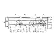
- 기판 위의 화소 영역에 배치된 화소 전극;상기 화소 전극의 제1 단 측에 배치되고 상기 화소 전극과 전기적으로 연결된 제m 데이터 배선(m은 자연수);상기 제m 데이터 배선과 부분적으로 중첩되어 상기 화소 영역에 배치된 플로팅 전극;상기 화소 전극의 제1 단과 마주하는 제2 단 측에 배치된 제m+1 데이터 배선; 및상기 제m+1 데이터 배선과 이격되어 상기 화소 영역에 배치된 스토리지 전극을 포함하는 표시 기판.
- 제1항에 있어서, 상기 플로팅 전극은 전기적으로 플로팅 되고, 상기 스토리지 전극은 전압이 인가되는 것을 특징으로 하는 표시 기판.
- 제1항에 있어서, 상기 제m 및 제m+1 데이터 배선들과 교차하는 제n 게이트 배선;상기 스토리지 전극과 전기적으로 연결되고, 상기 제n 게이트 배선과 평행하게 배치된 스토리지 배선; 및상기 제m 데이터 배선과 상기 제n 게이트 배선에 전기적으로 연결된 트랜지 스터를 더 포함하는 표시 기판.
- 제3항에 있어서, 상기 기판 상에 배치되어 상기 트랜지스터를 덮는 컬러 필터층을 더 포함하는 표시 기판.
- 제4항에 있어서, 상기 컬러 필터층은상기 기판 상에 배치된 상기 제m 및 제m+1 데이터 배선들을 덮는 차광 패턴; 및상기 화소 전극과 상기 기판 사이의 상기 화소 영역에 배치된 컬러 필터를 포함하는 것을 특징으로 하는 표시 기판.
- 제5항에 있어서, 상기 기판 상에 배치되어 상기 차광 패턴과 상기 컬러 필터를 덮는 오버 코팅층을 더 포함하고,상기 오버 코팅층은 상기 컬러 필터와 상기 화소 전극 사이에 배치되는 것을 특징으로 하는 표시 기판.
- 제3항에 있어서, 상기 화소 전극과 상기 트랜지스터를 전기적으로 연결하는 콘택 전극; 및상기 스토리지 배선과 전기적으로 연결되고 상기 콘택 전극과 중첩되는 돌출 전극을 더 포함하는 표시 기판.
- 기판 위의 화소 영역에 플로팅 전극, 상기 플로팅 전극과 마주하는 스토리지 전극을 포함하는 제1 도전 패턴을 형성하는 단계;상기 제1 도전 패턴이 형성된 상기 기판 위에 상기 플로팅 전극과 부분적으로 중첩되는 제m 데이터 배선, 상기 스토리지 전극과 이격된 제m+1 데이터 배선을 포함하는 제2 도전 패턴을 형성하는 단계; 및상기 제2 도전 패턴이 형성된 상기 기판 위의 상기 화소 영역에 상기 제1 데이터 배선과 전기적으로 연결된 화소 전극을 형성하는 단계를 포함하는 표시 기판의 제조 방법.
- 제8항에 있어서, 상기 제1 도전 패턴을 형성하는 단계는상기 제m 및 제m+1 데이터 배선들과 교차하는 제n 게이트 배선, 및 상기 스토리지 전극과 전기적으로 연결되고 상기 제n 게이트 배선과 평행한 스토리지 배선을 형성하는 단계를 포함하는 것을 특징으로 하는 표시 기판의 제조 방법.
- 제8항에 있어서, 상기 제n 게이트 배선과 상기 제m 데이터 배선과 전기적으로 연결된 트랜지스터를 형성하는 단계를 더 포함하는 것을 특징으로 하는 표시 기판의 제조 방법.
- 제10항에 있어서, 상기 화소 전극과 상기 트랜지스터를 전기적으로 연결하는 콘택 전극 및 상기 스토리지 배선과 전기적으로 연결되고 상기 콘택 전극과 중첩되는 돌출 전극을 더 형성하는 단계를 더 포함하는 표시 기판의 제조 방법.
- 제10항에 있어서, 상기 트랜지스터가 형성된 상기 기판 위에 컬러 필터층을 형성하는 단계를 더 포함하는 표시 기판의 제조 방법.
- 제12항에 있어서, 상기 컬러 필터층을 형성하는 단계는상기 트랜지스터가 형성된 상기 기판 위에 상기 제m 및 제m+1 데이터 배선을 덮도록 차광 패턴을 형성하는 단계; 및상기 기판 상의 상기 화소 영역에 컬러 필터를 형성하는 단계를 포함하는 것을 특징으로 하는 표시 기판의 제조 방법.
- 제13항에 있어서, 상기 차광 패턴과 상기 컬러 필터가 형성된 상기 기판 상에 오버 코팅층을 형성하는 단계를 더 포함하는 표시 기판의 제조 방법.
- 기판 위의 화소 영역에 배치된 화소 전극과, 상기 화소 전극의 제1 단 측에 배치되고 상기 화소 전극과 전기적으로 연결된 제m 데이터 배선(m은 자연수)과, 상기 제m 데이터 배선과 부분적으로 중첩되어 상기 화소 영역에 배치되고 전기적으로 플로팅 된 플로팅 전극, 상기 화소 전극의 제1 단과 마주하는 제2 단 측에 배치된 제m+1 데이터 배선, 및 상기 제m+1 데이터 배선과 이격되어 상기 화소 영역에 배치 되고 전압이 인가되는 스토리지 전극을 포함하는 표시 기판; 및상기 표시 기판과 대향하고 공통 전극을 포함하는 대향 기판을 포함하는 표시 장치.
- 제15항에 있어서, 상기 표시 기판은상기 제m 및 제m+1 데이터 배선들과 교차하는 제n 게이트 배선;상기 스토리지 전극과 전기적으로 연결되고, 상기 제n 게이트 배선과 평행하게 배치된 스토리지 배선; 및상기 제m 데이터 배선과 상기 제n 게이트 배선에 전기적으로 연결된 트랜지스터를 더 포함하는 표시 장치.
- 제16항에 있어서, 상기 기판 상에 배치되어 상기 트랜지스터를 덮는 컬러 필터층을 더 포함하는 표시 장치.
- 제17항에 있어서, 상기 컬러 필터층은상기 기판 상에 배치된 상기 제m 및 제m+1 데이터 배선들을 덮는 차광 패턴; 및상기 화소 전극과 상기 기판 사이의 상기 화소 영역에 배치된 컬러 필터를 포함하는 것을 특징으로 하는 표시 장치.
- 제18항에 있어서, 상기 기판 상에 배치되어 상기 차광 패턴과 상기 컬러 필터를 덮는 오버 코팅층을 더 포함하고, 상기 오버 코팅층은 상기 컬러 필터와 상기 화소 전극 사이에 배치되는 것을 특징으로 하는 표시 장치.
- 제16항에 있어서, 상기 표시 기판은상기 화소 전극과 상기 트랜지스터를 서로 전기적으로 연결하는 콘택 전극; 및상기 스토리지 배선과 전기적으로 연결되고 상기 콘택 전극과 중첩되는 돌출 전극을 더 포함하는 표시 장치.
Priority Applications (3)
| Application Number | Priority Date | Filing Date | Title |
|---|---|---|---|
| KR1020090100164A KR20110043166A (ko) | 2009-10-21 | 2009-10-21 | 표시 기판, 이의 제조 방법 및 이를 포함하는 표시 장치 |
| US12/893,423 US8698158B2 (en) | 2009-10-21 | 2010-09-29 | Display substrate, method of manufacturing the same, and display apparatus having the same |
| CN201010514704.2A CN102073181B (zh) | 2009-10-21 | 2010-10-21 | 显示基板、其制造方法以及具有该显示基板的显示设备 |
Applications Claiming Priority (1)
| Application Number | Priority Date | Filing Date | Title |
|---|---|---|---|
| KR1020090100164A KR20110043166A (ko) | 2009-10-21 | 2009-10-21 | 표시 기판, 이의 제조 방법 및 이를 포함하는 표시 장치 |
Publications (1)
| Publication Number | Publication Date |
|---|---|
| KR20110043166A true KR20110043166A (ko) | 2011-04-27 |
Family
ID=43878618
Family Applications (1)
| Application Number | Title | Priority Date | Filing Date |
|---|---|---|---|
| KR1020090100164A KR20110043166A (ko) | 2009-10-21 | 2009-10-21 | 표시 기판, 이의 제조 방법 및 이를 포함하는 표시 장치 |
Country Status (3)
| Country | Link |
|---|---|
| US (1) | US8698158B2 (ko) |
| KR (1) | KR20110043166A (ko) |
| CN (1) | CN102073181B (ko) |
Cited By (1)
| Publication number | Priority date | Publication date | Assignee | Title |
|---|---|---|---|---|
| US11619850B2 (en) | 2020-05-26 | 2023-04-04 | Samsung Display Co., Ltd. | Display device |
Families Citing this family (9)
| Publication number | Priority date | Publication date | Assignee | Title |
|---|---|---|---|---|
| WO2014054569A1 (ja) * | 2012-10-03 | 2014-04-10 | シャープ株式会社 | 半導体装置及び表示装置 |
| KR20140044453A (ko) * | 2012-10-05 | 2014-04-15 | 삼성디스플레이 주식회사 | 표시 기판 및 이를 포함하는 액정 표시 패널 |
| KR102164311B1 (ko) | 2013-12-06 | 2020-10-13 | 삼성디스플레이 주식회사 | 액정 표시 장치 |
| KR102123979B1 (ko) * | 2013-12-09 | 2020-06-17 | 엘지디스플레이 주식회사 | 리페어 구조를 갖는 유기발광표시장치 |
| KR20160106798A (ko) * | 2015-03-02 | 2016-09-13 | 삼성디스플레이 주식회사 | 표시 장치 |
| CN105116655B (zh) * | 2015-09-22 | 2017-04-12 | 深圳市华星光电技术有限公司 | 液晶显示面板、阵列基板及其制造方法 |
| KR102596074B1 (ko) * | 2016-07-18 | 2023-11-01 | 삼성디스플레이 주식회사 | 표시 기판 및 이의 제조 방법 |
| CN107037641B (zh) * | 2017-05-12 | 2020-04-24 | 京东方科技集团股份有限公司 | 阵列基板、显示面板和显示装置 |
| KR102509111B1 (ko) * | 2018-05-17 | 2023-03-13 | 삼성디스플레이 주식회사 | 표시 장치 |
Family Cites Families (7)
| Publication number | Priority date | Publication date | Assignee | Title |
|---|---|---|---|---|
| JP3401589B2 (ja) * | 1998-10-21 | 2003-04-28 | 株式会社アドバンスト・ディスプレイ | Tftアレイ基板および液晶表示装置 |
| CN100383647C (zh) * | 2004-01-13 | 2008-04-23 | 鸿富锦精密工业(深圳)有限公司 | 平面内切换型液晶显示装置及其采用的存储电容 |
| KR100614332B1 (ko) * | 2004-03-30 | 2006-08-18 | 엘지.필립스 엘시디 주식회사 | 액정표시장치 및 그 제조방법 |
| JP4858820B2 (ja) * | 2006-03-20 | 2012-01-18 | 日本電気株式会社 | アクティブマトリクス基板及び液晶表示装置並びにその製造方法 |
| KR20080007813A (ko) * | 2006-07-18 | 2008-01-23 | 삼성전자주식회사 | 박막 트랜지스터 어레이 기판 |
| US8400599B2 (en) * | 2006-08-16 | 2013-03-19 | Samsung Display Co., Ltd. | Liquid crystal display panel having a light blocking electrode |
| KR20080015696A (ko) * | 2006-08-16 | 2008-02-20 | 삼성전자주식회사 | 액정 표시 장치 |
-
2009
- 2009-10-21 KR KR1020090100164A patent/KR20110043166A/ko active Search and Examination
-
2010
- 2010-09-29 US US12/893,423 patent/US8698158B2/en not_active Expired - Fee Related
- 2010-10-21 CN CN201010514704.2A patent/CN102073181B/zh not_active Expired - Fee Related
Cited By (1)
| Publication number | Priority date | Publication date | Assignee | Title |
|---|---|---|---|---|
| US11619850B2 (en) | 2020-05-26 | 2023-04-04 | Samsung Display Co., Ltd. | Display device |
Also Published As
| Publication number | Publication date |
|---|---|
| CN102073181A (zh) | 2011-05-25 |
| US20110089424A1 (en) | 2011-04-21 |
| US8698158B2 (en) | 2014-04-15 |
| CN102073181B (zh) | 2016-06-01 |
Similar Documents
| Publication | Publication Date | Title |
|---|---|---|
| KR20110043166A (ko) | 표시 기판, 이의 제조 방법 및 이를 포함하는 표시 장치 | |
| US7956945B2 (en) | Array substrate for liquid crystal display device | |
| US8071406B2 (en) | Array substrate and method of manufacturing the same | |
| JP5392670B2 (ja) | 液晶表示装置及びその製造方法 | |
| US8493540B2 (en) | Display panel and method of manufacturing the same | |
| US8502932B2 (en) | Liquid crystal display device and manufacturing and repairing methods thereof | |
| KR20110086937A (ko) | 표시 기판 및 이의 제조 방법 | |
| EP3279721B1 (en) | Array substrate and manufacturing method therefor, and display device | |
| JP2011186279A (ja) | 液晶表示パネル | |
| KR20100062284A (ko) | 표시기판, 이의 제조방법 및 이를 갖는 표시패널 | |
| JP2015108765A (ja) | 表示装置 | |
| JP2009175568A (ja) | 液晶表示装置 | |
| KR20140053667A (ko) | 박막 트랜지스터 표시판 및 그 제조 방법 | |
| KR20090082539A (ko) | 표시 기판, 이의 제조 방법 및 이를 구비한 액정표시패널 | |
| KR20090117314A (ko) | 표시 기판 및 이의 제조 방법 | |
| KR100951840B1 (ko) | 액정표시장치 | |
| KR20130063404A (ko) | 박막 트랜지스터 액정표시장치 및 이의 제조방법 | |
| KR20080003075A (ko) | 액정표시장치 및 그 제조방법 | |
| KR101172048B1 (ko) | 액정 표시패널 및 그 제조방법 | |
| JP2009169162A (ja) | 液晶表示装置 | |
| KR20110051785A (ko) | 액정표시장치 및 그 제조방법 | |
| KR20120076174A (ko) | 컬럼 스페이서를 갖는 액정표시장치 및 이의 제조방법 | |
| KR20130010704A (ko) | 게이트 인 패널 구조 액정표시장치용 어레이 기판 | |
| KR101374940B1 (ko) | 액정표시장치 | |
| KR101255699B1 (ko) | 프린지 필드 스위칭 모드의 액정 표시 장치 |
Legal Events
| Date | Code | Title | Description |
|---|---|---|---|
| PA0109 | Patent application |
Patent event code: PA01091R01D Comment text: Patent Application Patent event date: 20091021 |
|
| PG1501 | Laying open of application | ||
| N231 | Notification of change of applicant | ||
| PN2301 | Change of applicant |
Patent event date: 20120913 Comment text: Notification of Change of Applicant Patent event code: PN23011R01D |
|
| A201 | Request for examination | ||
| PA0201 | Request for examination |
Patent event code: PA02012R01D Patent event date: 20140827 Comment text: Request for Examination of Application Patent event code: PA02011R01I Patent event date: 20091021 Comment text: Patent Application |
|
| E902 | Notification of reason for refusal | ||
| PE0902 | Notice of grounds for rejection |
Comment text: Notification of reason for refusal Patent event date: 20150918 Patent event code: PE09021S01D |
|
| AMND | Amendment | ||
| E601 | Decision to refuse application | ||
| PE0601 | Decision on rejection of patent |
Patent event date: 20160331 Comment text: Decision to Refuse Application Patent event code: PE06012S01D Patent event date: 20150918 Comment text: Notification of reason for refusal Patent event code: PE06011S01I |
|
| AMND | Amendment | ||
| PX0901 | Re-examination |
Patent event code: PX09011S01I Patent event date: 20160331 Comment text: Decision to Refuse Application Patent event code: PX09012R01I Patent event date: 20151111 Comment text: Amendment to Specification, etc. |
|
| PX0601 | Decision of rejection after re-examination |
Comment text: Decision to Refuse Application Patent event code: PX06014S01D Patent event date: 20160531 Comment text: Amendment to Specification, etc. Patent event code: PX06012R01I Patent event date: 20160502 Comment text: Decision to Refuse Application Patent event code: PX06011S01I Patent event date: 20160331 Comment text: Amendment to Specification, etc. Patent event code: PX06012R01I Patent event date: 20151111 Comment text: Notification of reason for refusal Patent event code: PX06013S01I Patent event date: 20150918 |