KR20100084525A - Semiconductor device with (110)-oriented silicon - Google Patents
Semiconductor device with (110)-oriented silicon Download PDFInfo
- Publication number
- KR20100084525A KR20100084525A KR1020107009063A KR20107009063A KR20100084525A KR 20100084525 A KR20100084525 A KR 20100084525A KR 1020107009063 A KR1020107009063 A KR 1020107009063A KR 20107009063 A KR20107009063 A KR 20107009063A KR 20100084525 A KR20100084525 A KR 20100084525A
- Authority
- KR
- South Korea
- Prior art keywords
- layer
- type
- silicon
- heavily doped
- forming
- Prior art date
- Legal status (The legal status is an assumption and is not a legal conclusion. Google has not performed a legal analysis and makes no representation as to the accuracy of the status listed.)
- Ceased
Links
Images


Classifications
-
- H—ELECTRICITY
- H10—SEMICONDUCTOR DEVICES; ELECTRIC SOLID-STATE DEVICES NOT OTHERWISE PROVIDED FOR
- H10D—INORGANIC ELECTRIC SEMICONDUCTOR DEVICES
- H10D62/00—Semiconductor bodies, or regions thereof, of devices having potential barriers
- H10D62/40—Crystalline structures
- H10D62/405—Orientations of crystalline planes
-
- H—ELECTRICITY
- H10—SEMICONDUCTOR DEVICES; ELECTRIC SOLID-STATE DEVICES NOT OTHERWISE PROVIDED FOR
- H10D—INORGANIC ELECTRIC SEMICONDUCTOR DEVICES
- H10D12/00—Bipolar devices controlled by the field effect, e.g. insulated-gate bipolar transistors [IGBT]
- H10D12/01—Manufacture or treatment
- H10D12/031—Manufacture or treatment of IGBTs
- H10D12/032—Manufacture or treatment of IGBTs of vertical IGBTs
- H10D12/038—Manufacture or treatment of IGBTs of vertical IGBTs having a recessed gate, e.g. trench-gate IGBTs
-
- H—ELECTRICITY
- H10—SEMICONDUCTOR DEVICES; ELECTRIC SOLID-STATE DEVICES NOT OTHERWISE PROVIDED FOR
- H10D—INORGANIC ELECTRIC SEMICONDUCTOR DEVICES
- H10D18/00—Thyristors
- H10D18/01—Manufacture or treatment
-
- H—ELECTRICITY
- H10—SEMICONDUCTOR DEVICES; ELECTRIC SOLID-STATE DEVICES NOT OTHERWISE PROVIDED FOR
- H10D—INORGANIC ELECTRIC SEMICONDUCTOR DEVICES
- H10D30/00—Field-effect transistors [FET]
- H10D30/01—Manufacture or treatment
- H10D30/021—Manufacture or treatment of FETs having insulated gates [IGFET]
- H10D30/028—Manufacture or treatment of FETs having insulated gates [IGFET] of double-diffused metal oxide semiconductor [DMOS] FETs
- H10D30/0291—Manufacture or treatment of FETs having insulated gates [IGFET] of double-diffused metal oxide semiconductor [DMOS] FETs of vertical DMOS [VDMOS] FETs
- H10D30/0297—Manufacture or treatment of FETs having insulated gates [IGFET] of double-diffused metal oxide semiconductor [DMOS] FETs of vertical DMOS [VDMOS] FETs using recessing of the gate electrodes, e.g. to form trench gate electrodes
-
- H—ELECTRICITY
- H10—SEMICONDUCTOR DEVICES; ELECTRIC SOLID-STATE DEVICES NOT OTHERWISE PROVIDED FOR
- H10D—INORGANIC ELECTRIC SEMICONDUCTOR DEVICES
- H10D30/00—Field-effect transistors [FET]
- H10D30/60—Insulated-gate field-effect transistors [IGFET]
- H10D30/64—Double-diffused metal-oxide semiconductor [DMOS] FETs
- H10D30/66—Vertical DMOS [VDMOS] FETs
- H10D30/668—Vertical DMOS [VDMOS] FETs having trench gate electrodes, e.g. UMOS transistors
-
- H—ELECTRICITY
- H10—SEMICONDUCTOR DEVICES; ELECTRIC SOLID-STATE DEVICES NOT OTHERWISE PROVIDED FOR
- H10D—INORGANIC ELECTRIC SEMICONDUCTOR DEVICES
- H10D64/00—Electrodes of devices having potential barriers
- H10D64/111—Field plates
- H10D64/117—Recessed field plates, e.g. trench field plates or buried field plates
-
- H—ELECTRICITY
- H10—SEMICONDUCTOR DEVICES; ELECTRIC SOLID-STATE DEVICES NOT OTHERWISE PROVIDED FOR
- H10D—INORGANIC ELECTRIC SEMICONDUCTOR DEVICES
- H10D64/00—Electrodes of devices having potential barriers
- H10D64/20—Electrodes characterised by their shapes, relative sizes or dispositions
- H10D64/23—Electrodes carrying the current to be rectified, amplified, oscillated or switched, e.g. sources, drains, anodes or cathodes
- H10D64/251—Source or drain electrodes for field-effect devices
- H10D64/252—Source or drain electrodes for field-effect devices for vertical or pseudo-vertical devices
-
- H—ELECTRICITY
- H10—SEMICONDUCTOR DEVICES; ELECTRIC SOLID-STATE DEVICES NOT OTHERWISE PROVIDED FOR
- H10D—INORGANIC ELECTRIC SEMICONDUCTOR DEVICES
- H10D64/00—Electrodes of devices having potential barriers
- H10D64/20—Electrodes characterised by their shapes, relative sizes or dispositions
- H10D64/27—Electrodes not carrying the current to be rectified, amplified, oscillated or switched, e.g. gates
- H10D64/311—Gate electrodes for field-effect devices
- H10D64/411—Gate electrodes for field-effect devices for FETs
- H10D64/511—Gate electrodes for field-effect devices for FETs for IGFETs
- H10D64/512—Disposition of the gate electrodes, e.g. buried gates
- H10D64/513—Disposition of the gate electrodes, e.g. buried gates within recesses in the substrate, e.g. trench gates, groove gates or buried gates
-
- H10P90/1916—
-
- H10W10/181—
-
- H10P50/644—
Landscapes
- Electrodes Of Semiconductors (AREA)
- Recrystallisation Techniques (AREA)
Abstract
금속 기판 상에 고농도 도핑된 P-형 (110) 반도체층 상에 반도체 소자를 형성하는 방법은 제1 지지 기판을 제공하는 단계 및 제1 지지 기판 상에 P-형 고농도 도핑된 (110) 실리콘층을 형성하는 단계를 포함한다. 제1 지지 기판의 적어도 최상층은 P-형 고농도 도핑된 (110) 실리콘층에 대하여 선택적 식각 공정에 의하여 제거된다. (110) 실리콘층 내에 및 그 상에 수직 반도체 소자 구조가 형성된다. 수직 소자 구조는 최상 금속층을 포함하고, <110> 방향으로의 전류 전도에 의하여 특징된다. 방법은, 제2 지지 기판을 최상 금속층에 부착하는 단계 및 P-형 고농도 도핑된 (110) 실리콘층의 표면을 노출하고, 금속층이 표면 상에 형성되도록, 기계적 연마 및 선택적 식각 공정을 이용하여 제1 지지 기판을 제거하는 단계를 포함한다.A method of forming a semiconductor device on a heavily doped P-type (110) semiconductor layer on a metal substrate includes providing a first support substrate and a P-type heavily doped (110) silicon layer on the first support substrate. Forming a step. At least the top layer of the first support substrate is removed by a selective etching process with respect to the P-type heavily doped (110) silicon layer. Vertical semiconductor device structures are formed in and on the (110) silicon layer. The vertical element structure comprises a top metal layer and is characterized by current conduction in the <110> direction. The method comprises the steps of attaching a second support substrate to the topmost metal layer and exposing the surface of the P-type heavily doped (110) silicon layer and using a mechanical polishing and selective etching process such that the metal layer is formed on the surface. 1 removing the support substrate.
Description
본 발명은 일반적으로 반도체 소자들에 관한 것이고, 보다 상세하게는 (110) 배향 실리콘 내에 트렌치 FET들을 제조하기 위한 방법과 구조에 관한 것이다.FIELD OF THE INVENTION The present invention generally relates to semiconductor devices, and more particularly, to a method and structure for fabricating trench FETs in (110) oriented silicon.
<관계 출원과의 상호 참조><Cross Reference with Related Applications>
본 출원은 2007년9월27일 출원되고 공통 양수된 미국임시출원번호 제60/975,739호의 이익을 주장하고, 그 전체 내용은 모든 목적을 위하여 참조로서 본 명세서와 결합된다.This application claims the benefit of US Provisional Application No. 60 / 975,739, filed on September 27, 2007 and commonly assigned, the entire contents of which are incorporated herein by reference for all purposes.
종래의 반도체 제조는 기판들 상에 반도체 구조들을 형성하기 위하여 많은 공정들을 이용한다. 특정한 장치들에 있어서, 기판은 전류 전도 경로의 부분으로 사용된다. 예를 들어, 기판은 분리된 장치 어플리케이션들과 집적회로들에 사용되는 중요한 반도체 구조인 고상 스위치를 가지고 중요한 기능을 한다. 고상 스위치들은, 예를 들어, 전력 금속-산화물-반도체 전계효과 트랜지스터(power metal-oxide-semiconductor field effect transistor, power MOSFET), 절연된-게이트 바이폴라 트랜지스터(insulated-gate bipolar transistor, IGBT), 및 다양한 사이리스터들(thyristors)을 포함한다. 전력 스위치들의 특정한 성능들 중에 일부는 온-저항(즉, 드레인-투-소스 온-저항(drain-to-source on-resistance), RDSon), 항복 전압, 및 스위칭 속도이다.Conventional semiconductor fabrication uses many processes to form semiconductor structures on substrates. In certain devices, the substrate is used as part of the current conducting path. For example, substrates play an important role with solid state switches, which are important semiconductor structures used in discrete device applications and integrated circuits. Solid state switches are, for example, power metal-oxide-semiconductor field effect transistors (power MOSFETs), insulated-gate bipolar transistors (IGBTs), and various types. Thyristors. Some of the specific capabilities of power switches are on-resistance (ie, drain-to-source on-resistance, R DSon ), breakdown voltage, and switching speed.
일반적으로, 통상적인 MOSFET의 스위칭 속도, 온-저항, 항복 전압, 및 소비 전력은 레이아웃, 치수들, 및 물질들에 의하여 영향을 받는다. 공업 디자인 현장에서는, 전도 전력 손실을 최소화하고, 전류 밀도들을 증가시키도록 MOSFET의 온-저항을 가능한 적게 유지하고자 한다. 예를 들어, 수직 전력 MOSFET들에 있어서, 온-저항은 채널 저항, 드리프트(drift) 영역(예를 들어, 에피택셜층) 저항, 및 기판 저항과 같은 여러 가지 저항들로 구성된다. 이러한 수직 전력 MOSFET(또한 다른 MOSFET들)의 온-저항은 드레인에서 소스로의 전도 경로를 형성하도록 사용된 물질들의 유형들과 치수들에 직접적으로 영향을 받는다. 따라서, 수직 전력 장치들에 대하여, 예를 들어 전력 MOSFET에 대하여, 기판은 중요한 성능 요소이다.In general, the switching speed, on-resistance, breakdown voltage, and power consumption of a typical MOSFET are affected by layout, dimensions, and materials. In an industrial design field, one wants to keep the MOSFET's on-resistance as low as possible to minimize conduction power losses and increase current densities. For example, in vertical power MOSFETs, the on-resistance consists of various resistors, such as channel resistance, drift region (eg, epitaxial layer) resistance, and substrate resistance. The on-resistance of this vertical power MOSFET (also other MOSFETs) is directly affected by the types and dimensions of materials used to form the conduction path from drain to source. Thus, for vertical power devices, for example for power MOSFETs, the substrate is an important performance factor.
다양한 기판 물질들을 이용한 수직 전력 장치들을 형성하기 위하여 종래의 기술들을 사용해왔어도, 이러한 종래의 기술들과 관련된 한계들이 있다. 이러한 한계들의 일부는 하기에 상세하게 설명되어 있다. Although conventional techniques have been used to form vertical power devices using various substrate materials, there are limitations associated with these conventional techniques. Some of these limitations are described in detail below.
따라서, 간단한 제조 공정을 유지하면서, 원하는 기판 특성들을 가지는 수직 소자들을 형성하기 위한 개선된 기술들이 요구된다.Thus, there is a need for improved techniques for forming vertical devices having desired substrate characteristics while maintaining a simple manufacturing process.
본 발명이 이루고자 하는 기술적 과제는, 향상된 기판 특성을 가지는 수직 소자들을 형성하기 위하여, (110) 배향 실리콘 내에 트렌치 FET들을 제조하기 위한 방법과 구조를 제공하는 것이다.It is an object of the present invention to provide a method and structure for fabricating trench FETs in (110) oriented silicon to form vertical devices with improved substrate properties.
본 발명의 일부 실시예들에 따라서, P-형 수직 반도체 소자들의 소자 특성들을 개선하기 위하여 (110) P-형 물질 내의 더 높은 정공 이동도와 고농도 도핑된 (110) P-형 물질의 낮은 저항을 결합하기 위한 다양한 기술들이 개시된다.In accordance with some embodiments of the present invention, in order to improve device characteristics of P-type vertical semiconductor devices, higher hole mobility in (110) P-type material and low resistance of heavily doped (110) P-type material may be employed. Various techniques for combining are disclosed.
본 발명의 일실시예에 따라서, 고농도 도핑된 P-형 (110) 반도체층 상에 반도체 소자를 형성하기 위한 방법이 제공된다. 상기 방법은 (110)의 표면 결정 배향 및 제1 전도도에 의하여 특성화되고 고농도 도핑된 제1 P-형 반도체층을 제공하는 단계를 포함한다. 또한, 상기 방법은 제1 P-형 반도체층 상에 제2 P-형 반도체층을 형성하는 단계를 포함한다. 상기 제2 P-형 반도체층은 (110)의 표면 결정 배향을 가지고, 상기 제1 전도도에 비하여 낮은 전도도에 의하여 특성화된다. 상기 방법은 상기 제2 P-형 반도체층 상에 최상 도전층을 형성하는 단계 및 상기 제1 P-형 반도체층 하측에 바닥 도전층을 형성하는 단계를 더 포함한다. 상기 최상 도전층으로부터 상기 제2 P-형 반도체층을 통하여 상기 바닥 도전층까지의 전류 전도는, (110) 결정면 상에서 <110> 결정 배향을 따르는 정공 이동도에 의하여 특성화된다.In accordance with one embodiment of the present invention, a method is provided for forming a semiconductor device on a heavily doped P-
구체적인 일 실시예에 있어서, 상기 방법은, 제1 지지 기판을 제공하는 단계 및 상기 제1 지지 기판 상에 P-형 고농도 도핑된 (110) 실리콘층을 형성하는 단계를 포함한다. 상기 제1 지지 기판의 적어도 최상층은 상기 P-형 고농도 도핑된 (110) 실리콘층에 대하여 선택적 식각 공정에 의하여 제거될 수 있다. 이어서, 상기 P-형 고농도 도핑된 (110) 실리콘층 내에 및 그 상에 수직 반도체 소자 구조를 형성한다. 상기 소자 구조는 최상 금속층을 포함하고, (110) 면 상에서 <110> 방향으로의 전류 전도에 의하여 특성화된다. 상기 방법은 상기 최상 금속층에 제2 지지 기판을 부착하는 단계, 및 상기 P-형 고농도 도핑된 (110) 실리콘층의 표면을 노출하도록 선택적 식각 공정을 이용하여 상기 제1 지지 기판을 제거하는 단계를 포함한다. 또한, 상기 방법은 상기 P-형 고농도 도핑된 (110) 실리콘층의 표면에 접촉하는 금속층을 제공하는 단계, 및 상기 제2 지지 기판을 제거하는 단계를 포함한다.In a specific embodiment, the method includes providing a first support substrate and forming a P-type heavily doped (110) silicon layer on the first support substrate. At least the top layer of the first support substrate may be removed by a selective etching process with respect to the P-type heavily doped (110) silicon layer. A vertical semiconductor device structure is then formed in and on the P-type heavily doped (110) silicon layer. The device structure comprises a top metal layer and is characterized by current conduction in the <110> direction on the (110) plane. The method includes attaching a second support substrate to the topmost metal layer, and removing the first support substrate using a selective etching process to expose the surface of the P-type heavily doped (110) silicon layer. Include. The method also includes providing a metal layer in contact with the surface of the P-type heavily doped (110) silicon layer, and removing the second support substrate.
일 실시예에 있어서, 상기 제1 지지 기판은 (100) 결정 배향, P-형 전도도, 및 저농도 도핑에 의하여 특성화된 실리콘 기판 상에 위치한 산화물층을 포함한다. 구체적인 실시예에 있어서, 상기 P-형 고농도 도핑된 (110) 실리콘층은 하기와 같이 형성된다. P-형 고농도 도핑된 (110) 실리콘층은 저농도 도핑된 P-형 (110) 기판인 제1 실리콘 기판 상에 형성된다. 제1 산화물층은 상기 P-형 고농도 도핑된 (110) 실리콘층 상에 형성된다. 상측 (110) 층 및 하측 (110) 층을 형성하기 위하여, 상기 고농도 도핑된 (110) 실리콘층 내부에 수소에 의하여 충분히 약화된 영역을 형성하여 상기 약화된 영역을 따라서 상기 고농도 도핑된 (110) 실리콘층을 분리하도록, 상기 고농도 도핑된 (110) 실리콘층 내로 수소 이온들을 주입한다. 일 실시예에 있어서, 상기 제1 지지 실리콘 기판 상에 제2 산화물층이 형성된다. 상기 방법은, 상기 제1 기판을 상기 제1 지지 실리콘 기판에 부착하는 단계, 및 상기 제1 지지 실리콘 기판 상의 상기 제2 실리콘 이산화물층에 부착된 상기 하측층이 잔류하도록, 상기 약화된 영역을 따라서 상기 P-형 고농도 도핑된 (110) 실리콘층을 분리하는 단계를 포함한다. 상기 하측 (110) 층은 P-형 전도도 및 고농도 도핑에 의하여 특성화된다. 구체적인 실시예에 있어서, 상기 실리콘 기판을 연마하고, 식각 저지층으로 상기 산화물층을 이용하여 잔류하는 상기 실리콘 기판을 식각하고, 또한 식각 저지층으로 상기 P-형 고농도 도핑된 (110) 실리콘층을 이용하여 잔류하는 상기 산화물층을 식각하여, 상기 제1 지지 기판을 제거한다.In one embodiment, the first support substrate comprises an oxide layer located on a silicon substrate characterized by (100) crystal orientation, P-type conductivity, and low concentration doping. In a specific embodiment, the P-type heavily doped (110) silicon layer is formed as follows. A P-type heavily doped (110) silicon layer is formed on the first silicon substrate, which is a lightly doped P-
다른 실시예에 있어서, 상기 제1 지지 기판은 (110) 결정 배향, P-형 전도도, 및 저농도 도핑에 의하여 특성화된 실리콘 기판을 포함하고, 상기 P-형 고농도 도핑된 (110) 실리콘층은 에피택셜 공정 또는 이온 주입 공정을 이용하여 형성된다. 구체적인 실시예에 있어서, 상기 실리콘 기판을 연마하고, 식각 저지층으로 상기 P-형 고농도 도핑된 (110) 실리콘층을 이용하여 잔류하는 상기 실리콘 기판을 식각하여, 상기 제1 지지 기판을 제거한다. 예를 들어, 상기 제1 지지 실리콘 기판은 KOH 또는 EDP를 포함하는 습식 식각 공정을 이용하여 제거될 수 있다.In another embodiment, the first support substrate comprises a silicon substrate characterized by (110) crystal orientation, P-type conductivity, and low concentration doping, wherein the P-type high concentration doped (110) silicon layer is epitaxial. It is formed using a tactical process or an ion implantation process. In a specific embodiment, the first support substrate is removed by polishing the silicon substrate and etching the remaining silicon substrate using the P-type heavily doped (110) silicon layer as an etch stop layer. For example, the first supporting silicon substrate may be removed using a wet etching process including KOH or EDP.
본 발명의 다른 실시예에 따라서, 수직 반도체 소자는 바닥 도전층 및 상기 바닥 도전층 상에 위치하는 제1 P-형 반도체층을 포함한다. 상기 제1 P-형 반도체층은 고농도 도핑되고, (110)의 표면 결정 배향 및 제1 전도도에 의하여 특성화된다. 상기 수직 반도체 소자는 상기 제1 P-형 반도체층 상에 위치한 제2 P-형 반도체층을 포함한다. 또한, 상기 제2 반도체층은 P-형이고, 상기 제1 전도도에 비하여 낮은 전도도에 의하여 특성화된다. 최상 금속층이 상기 제2 P-형 반도체층 상에 위치하고, 소자에 대한 최상측 콘택을 형성한다. 이러한 수직 반도체 소자에 있어서, 상기 최상 도전층으로부터 상기 제2 P-형 반도체층을 통하여 상기 바닥 도전층까지의 전류 전도는, (110) 결정면 상에서 <110> 결정 배향을 따르는 정공 이동도에 의하여 특성화된다.According to another embodiment of the present invention, the vertical semiconductor device includes a bottom conductive layer and a first P-type semiconductor layer positioned on the bottom conductive layer. The first P-type semiconductor layer is heavily doped and characterized by the surface crystal orientation and first conductivity of (110). The vertical semiconductor device includes a second P-type semiconductor layer located on the first P-type semiconductor layer. In addition, the second semiconductor layer is P-type and is characterized by low conductivity compared to the first conductivity. A top metal layer is located on the second P-type semiconductor layer and forms a top contact for the device. In this vertical semiconductor device, the current conduction from the uppermost conductive layer to the bottom conductive layer through the second P-type semiconductor layer is characterized by hole mobility along a <110> crystallographic orientation on a (110) crystal plane. do.
상기 수직 반도체 소자의 구체적인 실시예에 있어서, 상기 제1 P-형 반도체층은 1E17/cm3 또는 그 이상의 도핑 농도에 의하여 특성화된다. 다른 실시예에 있어서, 상기 제1 P-형 반도체층은 6E19/cm3 보다 높은 도핑 농도에 의하여 특성화된다.In a specific embodiment of the vertical semiconductor device, the first P-type semiconductor layer is characterized by a doping concentration of 1E17 / cm 3 or higher. In another embodiment, the first P-type semiconductor layer is characterized by a doping concentration higher than 6E19 / cm 3 .
구체적인 실시예에 있어서, 상기 수직 반도체 소자는 트렌치 게이트 MOSFET을 포함하고, 상기 트렌치 게이트 MOSFET은, 상기 제2 P-형 반도체 영역 내로 연장된 트렌치를 포함한다. 게이트 유전층은 상기 트렌치의 측벽과 바닥을 라이닝한다. 상기 트렌치 게이트 MOSFET은, 상기 트렌치 내에서 상기 게이트 유전층 상의 게이트 전극 및 상기 트렌치 내의 상기 게이트 전극의 각각의 측의 옆에 위치하는 P-형 소스 영역들을 포함한다. 또한, MOSFET은, P-형 드리프트 영역, 상기 드리프트 영역 상으로 연장된 N-형 바디 영역, 및 상기 바디 영역 내에 상기 트렌치에 인접하여 위치한 P-형 소스 영역들을 포함한다.In a specific embodiment, the vertical semiconductor device includes a trench gate MOSFET, and the trench gate MOSFET includes a trench extending into the second P-type semiconductor region. The gate dielectric layer lines the sidewalls and bottom of the trench. The trench gate MOSFET includes P-type source regions located next to each side of the gate electrode on the gate dielectric layer and the gate electrode in the trench in the trench. The MOSFET also includes a P-type drift region, an N-type body region extending over the drift region, and P-type source regions located adjacent to the trench in the body region.
다른 실시예에 있어서, 상기 수직 반도체 소자는 쉴디드 게이트 트렌치 MOSFET을 포함하고, 상기 쉴디드 게이트 트렌치 MOSFET은 상기 제2 반도체층 내로 연장된 트렌치를 포함한다. 쉴드 유전물은 상기 트렌치의 측벽 및 바닥 표면을 라이닝한다. 상기 쉴디드 게이트 트렌치 MOSFET은 상기 트렌치의 하측 부분에 위치하고, 상기 쉴드 유전물에 의하여 상기 제2 반도체층으로부터 절연된 쉴드 전극을 포함한다. 전극간 유전물은 상기 쉴드 전극 상에 위치하고, 게이트 유전물은 상기 트렌치 측벽의 상측 부분을 라이닝한다. 또한, 상기 쉴디드 게이트 트렌치 MOSFET은, 상기 전극간 유전물 상의 상기 트렌치의 상측 부분에 위치한 게이트 전극을 포함한다. 상기 게이트 전극은 상기 게이트 유전물에 의하여 상기 제2 P-형 반도체층으로부터 절연된다. 일 실시예에 있어서, 상기 제2 반도체층은, P-형 드리프트 영역, 상기 드리프트 영역 상으로 연장된 N-형 바디 영역, 및 상기 바디 영역 내에 상기 트렌치에 인접하여 위치한 P-형 소스 영역들을 포함한다.In another embodiment, the vertical semiconductor device includes a shielded gate trench MOSFET, and the shielded gate trench MOSFET includes a trench extending into the second semiconductor layer. Shield dielectric lining the sidewalls and bottom surface of the trench. The shielded gate trench MOSFET is positioned below the trench and includes a shield electrode insulated from the second semiconductor layer by the shield dielectric. An interelectrode dielectric is located on the shield electrode and a gate dielectric lining the upper portion of the trench sidewalls. The shielded gate trench MOSFET also includes a gate electrode located at an upper portion of the trench on the interelectrode dielectric. The gate electrode is insulated from the second P-type semiconductor layer by the gate dielectric. In one embodiment, the second semiconductor layer includes a P-type drift region, an N-type body region extending over the drift region, and P-type source regions located adjacent to the trench in the body region. do.
하기의 상세한 설명과 첨부된 도면들은 본 발명의 본질과 잇점들에 대한 이해를 더 넓게할 수 있다.The following detailed description and the annexed drawings may give a broader understanding of the nature and advantages of the present invention.
실시예에 따라, 본 발명은 사용될 수 있는 다양한 특징들을 포함한다. 이러한 특징들을 하기와 같다. 역전층 내에 높은 정공 이동도를 얻기 위하여, (110)/<110> 결정학적으로 구성된 실리콘 웨이퍼 상에 높은 이동도 p-채널 소자가 구현된다. 소자 온-저항으로의 저농도 도핑된 (110) 실리콘 기판의 영향이 감소된다. (110) 배향 금속 상의 실리콘 구조는 수직 전력 트렌치 소자들에서 게이트 전하를 증가시키지 않고 드레인-투-소스 온-저항을 실질적으로 개선할 수 있다.According to an embodiment, the present invention includes various features that can be used. These features are as follows. In order to obtain high hole mobility in the inversion layer, a high mobility p-channel device is implemented on a (110) / <110> crystallographically configured silicon wafer. The influence of the lightly doped (110) silicon substrate on device on-resistance is reduced. The silicon structure on the (110) oriented metal can substantially improve drain-to-source on-resistance without increasing gate charge in vertical power trench elements.
도 1은 본 발명의 일실시예에 따라서, P-형 트렌치 게이트 MOSFET을 도시하는 개략적인 단면도이다.
도 2는 본 발명의 다른 실시예에 따라서, P-형 쉴디드 게이트 트렌치 MOSFET을 도시하는 개략적인 단면도이다.
도 3a 및 도 3b는 본 발명의 일부 실시예들에 따라서, (110) 웨이퍼 내의 결정 배향들을 도시하는 개략도이다.
도 4a 내지 도 4f는 본 발명의 다른 실시예에 따라서, 고농도 도핑된 P-형 (110) 배향 기판 구조를 형성하기 위한 단순화된 공정을 도시하는 개략적인 단면도들이다.
도 5a 내지 도 5h는 본 발명의 다른 실시예에 따라서, 고농도 도핑된 P-형 (110) 배향 기판을 이용하여 수직 소자를 형성하기 위한 공정 흐름을 도시하는 개략적인 단면도들이다.
도 6 본 발명의 다른 실시예에 따라서, 붕소 농도의 함수로서 실리콘 식각 속도의 변화들을 도시하는 개략도이다.
도 7a 내지 도 7g 본 발명의 다른 실시예에 따른, 고농도 도핑된 P-형 (110) 배향 기판을 이용하여 수직 소자를 형성하기 위한 다른 공정 흐름을 도시하는 개략적인 단면도들이다.1 is a schematic cross-sectional view illustrating a P-type trench gate MOSFET, in accordance with an embodiment of the present invention.
2 is a schematic cross-sectional view illustrating a P-type shielded gate trench MOSFET, in accordance with another embodiment of the present invention.
3A and 3B are schematic diagrams showing crystal orientations in a (110) wafer, in accordance with some embodiments of the present invention.
4A-4F are schematic cross-sectional views illustrating a simplified process for forming a heavily doped P-type (110) oriented substrate structure, in accordance with another embodiment of the present invention.
5A-5H are schematic cross-sectional views illustrating a process flow for forming a vertical device using a heavily doped P-type (110) oriented substrate, in accordance with another embodiment of the present invention.
6 is a schematic diagram showing changes in silicon etch rate as a function of boron concentration.
7A-7G are schematic cross-sectional views illustrating another process flow for forming a vertical device using a heavily doped P-type (110) oriented substrate, in accordance with another embodiment of the present invention.
본 발명의 일부 실시예들에 따라서, (110) 면 상에서 <110> 방향으로 전류 전도에서 증가된 정공 이동도를 제공하고, 기판 저항을 감소시키고 우수한 오믹 콘택을 형성하기 위히여 고농도 도핑된(heavily doped) P-형 영역들을 제공하는 P-형 (110) 배향 실리콘 물질을 이용하여 수직 소자들을 형성하는 방법에 대한 다양한 기술들이 개시되어 있다. 일 실시예에 있어서, 고농도 도핑된 (110) 실리콘 물질의 층이 형성되고, 이어서 지지 기판에 이전된다. 후속의 수직 소자 제조에서는, 상기 지지 기판은 금속 콘택층과 함께 고농도 도핑된 (110) 실리콘 물질로 교체된다. 본 발명의 일 변형에 있어서, 고농도 도핑된 (110) 실리콘 물질의 층은 저농도 도핑된(110) 실리콘 기판 상에 형성된다. 소자 제조를 마친 후에, 상기 기판은 초기 기계적 연마를 종료한 후에 선택적 식각 공정을 이용하여 제거된다. 따라서, 본 발명의 실시예들은, P-형 수직 반도체 소자들의 소자 특성들을 개선하기 위하여, 상기 (110) P-형 물질 내의 더 높은 정공 이동도와 고농도 도핑된 (110) P-형 물질의 낮은 저항을 결합한다.According to some embodiments of the present invention, heavily doped to provide increased hole mobility in current conduction in the <110> direction on the (110) plane, to reduce substrate resistance and to form good ohmic contacts. doped) Various techniques are disclosed for forming vertical devices using a P-type (110) oriented silicon material that provides P-type regions. In one embodiment, a layer of heavily doped (110) silicon material is formed and then transferred to a support substrate. In subsequent vertical device fabrication, the support substrate is replaced with a heavily doped (110) silicon material with a metal contact layer. In one variation of the invention, a layer of heavily doped (110) silicon material is formed on the lightly doped (110) silicon substrate. After device fabrication is complete, the substrate is removed using a selective etching process after finishing initial mechanical polishing. Accordingly, embodiments of the present invention provide higher hole mobility in the (110) P-type material and lower resistance of the heavily doped (110) P-type material to improve device characteristics of the P-type vertical semiconductor devices. To combine.
실시예에 따라, 본 발명은 사용될 수 있는 다양한 특징들을 포함한다. 이러한 특징들을 하기와 같다.According to an embodiment, the present invention includes various features that can be used. These features are as follows.
1. 역전층(inversion layer) 내에 높은 정공 이동도를 얻기 위하여, (110)/<110> 결정학적으로 구성된 실리콘 웨이퍼 상에 높은 이동도 p-채널 소자가 구현된다.1. In order to obtain high hole mobility in the inversion layer, a high mobility p-channel device is implemented on a (110) / <110> crystallographically configured silicon wafer.
2. 소자 온-저항으로의 저농도 도핑된 (110) 실리콘 기판의 영향이 감소된다.2. The influence of the lightly doped (110) silicon substrate on the device on-resistance is reduced.
3. (110) 배향 금속 상의 실리콘(silicon-on-metal, SOM) 구조는 수직 전력 트렌치 소자들에서 게이트 전하를 증가시키지 않고 드레인-투-소스 온-저항(Rdson)을 실질적으로 개선할 수 있다.3. Silicon-on-metal (SOM) structure on (110) oriented metal can substantially improve drain-to-source on-resistance (Rdson) without increasing gate charge in vertical power trench elements .
상술한 특징들은 하기의 하나 또는 그 이상의 실시예들에 나타난다. 이러한 특징들은 단지 예시적이며, 본 명세서에 청구된 범위를 한정하는 것은 아니다. 본 기술분야의 당업자는 다양한 변형들, 변화들, 대체물들이 있음을 이해할 수 있다.The above described features are shown in one or more embodiments below. These features are exemplary only and are not intended to limit the scope claimed herein. Those skilled in the art can appreciate that there are various variations, changes, and substitutions.
도 1은 본 발명의 일실시예에 따른 P-형 트렌치 게이트 MOSFET(100)을 도시하는 개략적인 단면도이다. 그러나, 본 발명의 원칙적인 기술들은 모든 공정 기술들을 이용하여 분리된 소자들 및 집적회로에 모두 적용될 수 있음을 이해하여야 한다. 본 명세서에 개시된 다른 모든 특징들에 있어서, 도면들에 도시된 다양한 요소들 및 구성요소들의 상대적인 치수들 및 크기들은 실제 치수들을 정확하게 반영하는 것은 아니며, 단지 설명하기 위한 것임을 이해하여야 한다. 도시된 바와 같이, MOSFET(100)은 트렌치들(102) 내에 형성된 게이트 전극들(G)을 포함한다. 트렌치들(102)은 N-웰 바디(body) 영역(104)의 최상 표면으로부터 연장되어 P-형 드리프트(drift) 또는 에피택셜 영역(106) 내에서 종료된다. 일 실시예에 있어서, 트렌치들(102)은 얇은 유전층들(108)로 라이닝되고, 도핑된 폴리실리콘과 같은 도전 물질(110)로 실질적으로 덮인다. P-형 소스 영역들(112)은 트렌치들(102)에 인접하여 N-웰 바디 영역(104) 내에 형성된다. MOSFET(100)은 N-웰 바디 영역(104) 내에 형성된 N+ 바디 영역(117)을 포함한다. MOSFET(100)은 금속 소스층(116)을 포함한다. MOSFET(100)의 드레인 터미널(D)은 P-형 고농도 도핑된 실리콘층(114) 상에 위치한 금속 기판(118)에 커플링된다. 에피택셜층(106) 및 바디 영역(104)은 고농도 도핑된 P-형 실리콘층(114) 상에 위치한 반도체 구조층(107)을 형성한다.1 is a schematic cross-sectional view illustrating a P-type
도 2는 본 발명의 다른 실시예에 따른 P-형 쉴디드(shielded) 게이트 트렌치 MOSFET(200)을 도시하는 개략적인 단면도이다. 도시된 바와 같이, MOSFET(200)은 트렌치들(202) 내에 형성된 게이트 전극들(G)을 포함한다. 트렌치들(202)은 N-웰 바디 영역(204)의 최상 표면으로부터 연장되어 P-형 드리프트 또는 에피택셜 영역(206) 내에서 종료된다. 일 실시예에 있어서, 트렌치들(202)의 상측 부분들은 얇은 게이트 유전층들(208)로 라이닝되고, 도핑된 폴리실리콘과 같은 도전 물질(210)로 실질적으로 덮이고, 이에 따라 게이트 전극들(G)을 형성한다. 도핑된 폴리실리콘과 같은 도전 물질로 구성된 쉴디드 게이트 전극들(211)은 쉴드 유전층들(209)에 의하여 트렌치들(202)의 하측 부분들로부터 절연된다. P-형 소스 영역들(212)은 트렌치들(202)에 인접하여 N-웰 바디 영역(204) 내에 형성된다. MOSFET(200)은 N-웰 바디 영역(204) 내에 형성된 N+ 바디 영역(217)을 포함한다. MOSFET(200)은 금속 소스층(216)을 포함한다. MOSFET(200)의 드레인 터미널(D)은 P-형 고농도 도핑된 실리콘층(214) 상에 위치한 금속 기판(218)에 커플링된다. 에피택셜층(206) 및 바디 영역(204)은 고농도 도핑된 P-형 실리콘층(214) 상에 위치한 반도체 구조층(207)을 형성한다.2 is a schematic cross-sectional view illustrating a P-type shielded
트렌치 MOSFET 기술 개발의 주안점은 온-저항 (Rdson) 및 게이트 전하, 특히 게이트-투-드레인(gate-to-drain) 전하(Qgd) 모두를 감소시키는 것이다. 예를 들어, 피치를 감소시킴에 의하여 트렌치 밀도가 증가됨에 함께 온-저항(Rdson)을 감소시킬 수 있다. 그러나, 이러한 시도는 종종 더 높은 게이트-투-드레인 전하(Qgd)를 함께 증가시킨다. 또한, 이는 고농도 바디 영역 및 소스 영역 모두에 대한 콘택 형성을 어렵게 한다. 또한, 이러한 피치 감소는, 고농도 바디 공정에 의하여 생성된 결함 때문에, 더 높은 누설 결함을 발생시킨다.The focus of the development of trench MOSFET technology is to reduce both the on-resistance (Rdson) and gate charges, especially the gate-to-drain charge (Q gd ). For example, by decreasing the pitch, the trench density can be increased, thereby reducing the on-resistance (Rdson). However, such attempts often increase the higher gate-to-drain charge Q gd together. In addition, this makes contact formation difficult for both high concentration body regions and source regions. This pitch reduction also results in higher leakage defects due to defects created by the high concentration body process.
본 발명의 일실시예에 따라서, 채널 저항이 감소되도록, 결정학적 <110> 방향으로 평탄면(노치, notch)를 가지는 (110)-배향 실리콘 웨이퍼들 상에 p-채널 트렌치 MOSFET 소자를 제조하는 방법을 제공한다. 상기 역전층 내의 정공 이동도는, <100> 방향의 (100) 면 ((100)/<100>)의 경우에 비하여, <110> 방향의 실리콘 (110) 면 상에서 두 배 이상일 수 있음이 알려져 있다. 정공 이동도와 채널 저항 사이의 관계는 하기의 관계식으로 나타난다.In accordance with one embodiment of the present invention, a p-channel trench MOSFET device is fabricated on (110) -oriented silicon wafers having flat surfaces (notches) in the crystallographic <110> direction so that the channel resistance is reduced. Provide a method. It is known that the hole mobility in the inversion layer may be more than doubled on the
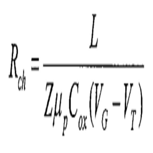
여기에서, L은 채널 길이, Z는 채널 폭, Cox 는 단위 면적당 게이트 산화층 캐패시턴스, VG 는 게이트 전압, μp 는 채널 영역 내의 정공 이동도, 및 VT 는 문턱 전압이다. 따라서, (110)/<110> 결정학적으로 구성된 웨이퍼들 상에 형성된 p-채널 소자들은, 개선된 정공 이동도(μp)에 의하여 상당히 감소된 채널 저항(Rch)을 가질 수 있다. Where L is the channel length, Z is the channel width, C ox is the gate oxide capacitance per unit area, V G is the gate voltage, μ p is the hole mobility in the channel region, and V T is the threshold voltage. Thus, p-channel devices formed on (110) / <110> crystallographically configured wafers may have a channel resistance R ch that is significantly reduced by improved hole mobility μ p .
도 3a에 도시된 바와 같이, 상기 <110> 결정학적 방향에 평행한 평탄면(노치)을 가지는 (110)-배향 실리콘 웨이퍼들을 이용하여 (110)/<110> 구성을 구현할 수 있다. 도 3b에 도시된 바와 같이, 이러한 유형의 웨이퍼들 상의 수직 트렌치들은 (110) 면들 상에 트렌치 바닥과 측벽을 모두 가지고, 트렌치 최상측으로부터 트렌치 바닥으로 (채널 방향) 흐르는 전류의 방향은 <110> 방향이다.As shown in FIG. 3A, a (110) / <110> configuration may be implemented using (110) -oriented silicon wafers having a flat surface (notch) parallel to the <110> crystallographic direction. As shown in FIG. 3B, the vertical trenches on these types of wafers have both trench bottoms and sidewalls on the (110) faces, and the direction of current flowing from the top of the trenches to the trench bottom (channel direction) is: Direction.
전력 트렌치 MOSFET 소자들에 상기 (110)/<110> 웨이퍼들을 적용함에 있어서의 한계는 고농도 붕소 도핑된 도핑된 (110) 배향 초크랄스키(Czochralski, CZ) 실리콘 웨이퍼들을 성장시키는 것이다. (110) 배향 실리콘 결정에 대한 매우 낮은 붕소 편석 계수 때문에, 붕소 결합은 매우 제한적이다. 이러한 잉곳의 저항은 수십 Ω-cm 의 범위이다. 수직 전력 트렌치 소자를 형성하기 위하여, 소자 온-저항에의 기판 영향을 감소시키기 위하여 고농도 붕소 도핑된 도핑된 (110) 배향 기판 및 기술을 가질 필요가 있다. 일실시예에 따라서, 본 발명은 감소된 채널 저항을 가지는 (110)-배향 실리콘 기판 상에 p-채널 트렌치 MOSFET 소자들을 형성하는 방법을 제공한다. 또한, 본 발명은 고농도 도핑된 (110)-배향 실리콘 기판를 이용하여 드레인 저항을 감소시키는 방법을 제공한다.The limitation in applying the (110) / <110> wafers to power trench MOSFET devices is to grow heavily boron doped (110) oriented Czochralski (CZ) silicon wafers. Because of the very low boron segregation coefficient for (110) oriented silicon crystals, boron bonds are very limited. The resistance of these ingots is in the range of tens of Ω-cm. In order to form vertical power trench devices, it is necessary to have a high concentration of boron doped doped (110) oriented substrates and techniques in order to reduce the substrate influence on device on-resistance. According to one embodiment, the present invention provides a method of forming p-channel trench MOSFET devices on a (110) -oriented silicon substrate having a reduced channel resistance. The present invention also provides a method of reducing drain resistance using a heavily doped (110) -oriented silicon substrate.
본 발명의 예시적인 실시예에 따른 고농도 도핑된 P-형 (110) 기판 구조를 이용한 전력 장치를 형성하는 공정 흐름을 도시한다. 100 mΩ-cm (도판트 농도 > 1 x 1017 cm-3) 보다 낮은 저항과 3.0 ㎛ 보다 낮은 두께를 가지는 에피층이 저농도 도핑된 (110) 배향 실리콘 기판 상에 성장한다. 이어서, 400Å 내지 500Å 범위의 두께를 가지는 열 실리콘 이산화물층이 상기 에피층의 최상층 상에 성장한다. 수소 이온들/분자들이 3 x 1016 cm-2 의 도즈 및 60 KeV 내지 170 KeV 범위의 에너지로 상기 실리콘 이산화물층을 통하여 주입된다. 참조의 용이함을 위하여, 이하에서는 이러한 웨이퍼를 씨드 웨이퍼로 부르기로 한다. 이어서, 상기 씨드 웨이퍼는, 실온에서 수행된 웨이퍼 직접 부착 기술을 이용하여, 1000Å 내지 2500 Å 범위의 두께의 열 실리콘 이산화물층이 상측에 있는 다른 실리콘 웨이퍼 (지지 기판)에 부착된다. 이어서, 상기 부착된 웨이퍼 쌍은 2 단계 저온 어닐링 과정을 거친다. 150℃ 내지 300℃ 범위의 온도에서의 10 시간 내지 20 시간 범위의 시간 동안의 제1 어닐링은 융합 부착 선-강화(fusion bond pre-strengthening)를 위하여 사용되고, 450℃ 온도에서의 45분 동안의 제2 어닐링은 수소 주입 에너지에 의하여 한정된 분리면을 따라서 상기 씨드 웨이퍼의 고농도 붕소 도핑된 도핑된 (110) 층의 분리하기 위하여 사용된다. 상기 이전된 고농도 붕소 도핑된 (110) 층의 두께는 수소 주입의 에너지에 의하여 한정되고, 구체적인 실시예에 있어서, 0.5 ㎛ 내지 약 1.5 ㎛ 범위이다. 이에 대한 상세한 설명은 하기에 기술하기로 한다.A process flow for forming a power device using a heavily doped P-
도 4a 내지 도 4f는 본 발명의 일 실시예에 따른 고농도 도핑된 P-형 (110) 배향 기판 구조를 형성하기 위한 단순화된 공정을 도시하는 개략적인 단면도들이다. 도 4a는 붕소와 같은 도판트들에 의하여 도핑될 수 있는 씨드 (110) 실리콘 물질(402)의 단면도를 도시한다. 구체적인 실시예에 있어서, 실리콘 물질(402)은 저농도 도핑된 P-형 실리콘 기판일 수 있다. 100 m Ω-cm (도판트 농도 > 1 x 1017 cm-3) 미만의 저항과 3.0 ㎛ 미만의 두께를 가지는 고농도 도핑된 P-형 에피층(404)이 저농도 도핑된 (110) 배향 실리콘 기판 상에 성장한다. 이를 대신하여, 실리콘 물질(402) 내에 도판트들을 주입하여 고농도 도핑된 층(404)이 형성될 수 있다. 이어서, 400 Å 내지 500 Å 범위의 두께를 가지는 열 실리콘 산화물층(406)이 고농도 도핑된 층(404)의 상에 성장된다. 수소 이온들/분자들이 3 x 1016 cm-2 의 도즈 및 60 KeV 내지 170 KeV 범위의 에너지로 상기 실리콘 이산화물층을 통하여 주입된다. 일 실시예에 있어서, 이하에서는, 층들(402, 404, 406)을 포함하는 상기 웨이퍼를 씨드 웨이퍼(407)로 지칭하기로 한다. 일 실시예에 있어서, 수소 주입은 에피층(404) 내의 점선으로 도시된 수소 리치 영역(405)을 생성한다. 도핑 수소 이온들이 실리콘 기판 내로 주입되는 예시적인 공정이 브루엘(Bruel)에 의한 미국등록번호 제5,374,564호에 개시되어 있고, 그 전체 내용은 모든 목적을 위하여 참조로서 본 명세서와 결합된다.4A-4F are schematic cross-sectional views illustrating a simplified process for forming a heavily doped P-
일 실시예에 있어서, 약 1 ㎛ 내지 2 ㎛ 범위의 예시적인 두께를 가지는 수소 리치 영역, 또는 분리가능 영역(405)을 형성하기 위하여, 수소 이온들의 농도가 충분한 깊이 및 에너지 포텐셜로 제공된다. 수소 취성 때문에, 분리가능 영역(405) 격자는 비-수소 도핑된 실리콘 격자에 비하여 약하다.In one embodiment, the concentration of hydrogen ions is provided at a sufficient depth and energy potential to form a hydrogen rich region, or
도 4b는 본 발명의 실시예들에 따른 제1 지지 기판(308)의 일실시예의 단면도를 도시한다. 일 실시예에 있어서, 제1 지지 기판(308)은 (100) 실리콘 기판이다. 다른 실시예에 있어서, 상기 (100) 실리콘 기판은 실리콘 이산화(SiO2) 층(305)으로 덮인다. 실리콘 이산화층(305)은 식각 저지층(etch stop) 층으로서 사용되고, 또한 효과적인 사용을 위하여 적절한 두께를 가질 수 있다. 예를 들어, 일 실시예에 있어서, 실리콘 이산화층(305)은 1000 Å 내지 2500 Å 범위일 수 있다. 다른 실시예에 있어서, 실리콘 이산화층(305)은 2500 Å 내지 4000 Å 범위일 수 있다. 실리콘 이산화층(305)은 모든 실리콘 이산화층 제조 공정을 이용하여 지지 기판(308) 상에 성장되거나 또는 증착될 수 있다. 예를 들어, 실리콘 이산화층(305)은 열산화 공정을 이용하여 성장될 수 있다.4B illustrates a cross-sectional view of one embodiment of a
도 4c에 있어서, 제1 지지 기판(308)과 산화물층(305)은 도 4a에 도시된 바와 같은 층들(402, 404, 406)을 포함하는 씨드 웨이퍼(407)에 부착된다. 구체적인 실시예에 있어서, 산화물층(306)을 형성하기 위하여, 산화물층들(305, 406)은 부착 공정에서 함께 부착된다. 이러한 부착은 모든 많은 부착 기술들을 이용하여 수행될 수 있다. 예를 들어, 친수성 표면을 가지는 실리콘 이산화층들(305, 406)을 형성하기 위한 습식 식각과 탈이온수(de-ionized water, DI water) 처리를 완료한 후에, 실리콘 이산화층(305) 및 씨드 웨이퍼(407)는 종래의 부착 기술들을 이용하여 실온에서 부착될 수 있다.In FIG. 4C, the
도 4d에 있어서, 두 개의 분리된 층들(114A, 114B) 내로 에피층(404)을 분리하도록, 분리 공정이 수행된다. 상기 분리 공정은 제1 지지 기판(308) 상에 고농도 도핑된 (110) P-형 실리콘의 하측 층(114B) 및 씨드 실리콘 물질(402) 상에 상기 에피층의 잔존하는 층 부분(114A)을 남긴다. 분리가능 영역(405)의 격자 구조를 파괴하기 위하여, 모든 분리 공정들을 이용하여 상기 분리 공정을 수행할 수 있다. 일 실시예에 있어서, 상기 분리 공정은 150℃ 내지 300℃ 범위의 온도로 약 5 시간 내지 10 시간 범위 동안에 씨드 웨이퍼(407)와 초기 기판(308)을 어닐링 하는 단계를 포함한다. 다른 실시예에 있어서, 상기 분리 공정은 450℃의 온도로 약 15 분 동안에 씨드 웨이퍼(407)와 제1 지지 기판(308)을 어닐링 하는 단계를 포함한다. 구체적인 실시예에 있어서, 부착된 웨이퍼 쌍은 두 단계의 낮은 온도 어닐링 과정을 겪는다. 150℃ 내지 300℃ 범위의 온도에서의 10 시간 내지 20 시간 범위의 시간 동안의 제1 어닐링은 융합 부착 선-강화를 위하여 사용되고, 450℃ 온도에서의 45분 동안의 제2 어닐링은 수소 주입 에너지에 의하여 한정된 분리면을 따라서 상기 씨드 웨이퍼의 고농도 붕소 도핑된 도핑된 (110) 층의 분리하기 위하여 사용된다. 이에 따라, 이전된 고농도 붕소 도핑된 도핑된 (110) 층의 두께는 수소 주입 에너지에 의하여 한정되고, 구체적인 실시예에 있어서 0.5 ㎛ 내지 약 3 ㎛ 범위이다.In FIG. 4D, a separation process is performed to separate the
도 4e 및 도 4f는 도 4d에 도시된 분리 공정에서 형성된 두 개의 부분들을 도시하는 개략적인 단면도이다. 도 4e에 있어서, 저농도 도핑된 P-형 (110) 실리콘 웨이퍼(402) 및 고농도 P-형 도핑된 (110) 에피층(114A)을 포함하는 복합 물질(420)을 형성한다. 일 실시예에 있어서, 복합 물질(420)은 도 4a의 씨드 웨이퍼(407)와 같은 다른 씨드 웨이퍼를 형성하기 위하여 사용될 수 있고, 또한 도 4a 내지 도 4d에 도시된 바와 같은 공정에서 반복적으로 사용될 수 있다. 도 4f는 제1 지지 기판(308) 상에 위치한 산화물층(306) 상에 위치한 고농도 도핑된 P-형 (110) 층(114B)을 포함하는 복합 물질(430)을 도시한다. 일 실시예에 있어서, 층(114B)은, 상업적으로 구할 수 있는 (110) 실리콘 웨이퍼들에 비하여 낮은, 8 mΩ-cm 의 저항을 가진다. 일 실시예에 있어서, 이러한 층은 수직 소자를 형성하기 위하여 사용되고, 후측 메타층(meta layer)에 대하여 우수한 오믹 콘택을 제공한다. 수직 소자를 형성하는 예시적인 방법이 하기에 설명된다. 4E and 4F are schematic cross-sectional views showing two portions formed in the separation process shown in FIG. 4D. In FIG. 4E, a
도 5a 내지 도 5h는 본 발명의 일 실시예에 따라서, 고농도 도핑된 P-형 (110) 배향 기판을 이용하여 수직 소자를 형성하기 위한 공정 흐름을 도시하는 개략적인 단면도들이다. 도 5a는 지지층(308) 상에 위치한 산화물층(306) 상에 고농도 도핑된 P-형 (110) 실리콘층(114B)을 가지는 도 4f의 반도체 프로세스 구조(430)의 일 실시예의 단면도를 도시한다. 일 실시예에 있어서, 지지층(308)은 저농도 도핑된 (100) 실리콘층일 수 있다. 구체적인 실시예에 있어서, 층(114B)은 1E17/cm3 또는 그 이상의 도핑 농도를 가진다. 일 실시예에 있어서, 도 5a이 구조는 도 4a 내지 도 4f에 개시된 공정을 이용하여 형성될 수 있다. 이를 대신하여, 다른 방법을 이용하여 도 5a의 구조가 형성될 수 있다.5A-5H are schematic cross-sectional views illustrating a process flow for forming a vertical device using a heavily doped P-type (110) oriented substrate, in accordance with an embodiment of the present invention. FIG. 5A shows a cross-sectional view of one embodiment of the
도 5b에 있어서, 저농도 도핑된 P-형 (110) 에피택셜층(106)이 도핑된 P-형 (110) 실리콘층(114B) 상에 형성된다. 선택적으로(Optionally), 에피택셜층(106)의 형성을 위한 실리콘층(114B)을 준비하기 위하여, 분리된 도핑된 실리콘층(114B)이 CVD 챔버 내에서 우선 처리된다. 보다 균일한 표면을 생성하기 위하여, 이러한 우선 처리가 사용될 수 있다.In FIG. 5B, a lightly doped P-
도 5c에 있어서, 반도체 소자들(702)이 에피택셜층(106) 내에 및 그 상에 형성되고, 반도체 구조층(107)을 형성한다. 반도체 구조층(107)의 형성은 모든 종래의 반도체 구조 형성 기술들에 의하여 수행될 수 있다. 예를 들어, 층 형성, 패터닝, 및 도핑과 같은 종래의 반도체 구조 형성 단계들을 이용하여, 에피택셜층(106) 상에 및/또는 그 내에 반도체 구조들(702)이 형성될 수 있다. 반도체 구조들(702)은 도핑된 실리콘층(114B) 상에 형성되거나 및/또는 도핑된 실리콘층(114B)에 통합되어 형성될 수 있다. 일 실시예에 있어서, 반도체 구조층(107)은, 도 1과 관련하여 상술한 바와 같이, 트렌치 게이트 MOSFET 구조들을 포함할 수 있다. 본 실시예에 있어서, 반도체 구조들(702) 각각은 트렌치 게이트 MOSFET이다. 다른 예에 있어서, 도 5c에 도시된 반도체 구조층(107)은, 도 2와 관련하여 상술한 바와 같이, 쉴디드 게이트 트렌치 MOSFET 구조들을 포함할 수 있다. 본 실시예에 있어서, 반도체 구조들(702) 각각은 쉴디드 게이트 트렌치 MOSFET이다. 하나의 선택적인 동작 구성에 있어서, MOSFET들에 대하여, 예를 들어, 금속층(116)이 반도체 구조들(702) 상에 형성된다. 금속층(116)은, 본 명세서에 개시된 바와 같은 모든 공정을 이용하여, 적용될 수 있다. 다른 실시예에 있어서, 소자층(107)을 형성한 후에, 초기 기판(308), 실리콘 이산화층(306), 도핑된 실리콘층(114B), 및 반도체 구조층(107)은 함께 다른 중간의 반도체 프로세스 구조(507)를 형성한다.In FIG. 5C,
도 5d에 있어서, 공정을 위한 반도체 프로세스 구조(507)를 지지하기 위하여, 제2 지지 기판(802), 예를 들어, 유리 웨이퍼는 반도체 구조층(107) 상에 금속층(116)에 실장된다. 예를 들어, 제2 지지 기판(802)은, 공정을 위한 중간 반도체 프로세스 구조를 안전하게 유지하도록 충분한 강도의 접착을 제공하는 UV 풀어지는(releasable) 양면 테이프를 이용하여 반도체 프로세스 구조들(507)에 실장된다.In FIG. 5D, a
도 5e에 있어서, 초기 지지층(308), 예를 들어, (100) 실리콘 기판은 기판 박형화 공정에 의하여 박형화된다. 선택적으로(Optionally), 일 실시예에 있어서, 더 얇은 기판(308A)을 형성하기 위하여, 기계적 폴리싱(polishing)/연마(grinding)와 같은 기계적 박형화 공정을 이용하여 초기 기판(308)은 박형화된다. 초기 기판(308)은 예를 들어, 약 8 밀(mil)로 박형화될 수 있고, 화학제들을 이용하여 빠르게 제거될 수 있다.In FIG. 5E, the
도 5f에 있어서, 잔존하는 기판(308A)은 기판 식각 공정을 이용하여 제거된다. 일 공정에 있어서, 식각 저지층으로 매립 실리콘 이산화층(306)을 이용한 화학 식각 공정으로 기판(308A)을 화학적 식각하여 기판(308A)을 제거한다. 실리콘 이산화층(306)이 상기 화학 식각 공정을 중단하도록 구성되는 경우에는, 초기 기판(308A)을 식각하도록 사용된 화학물에 의하여 실리콘층(114B) 및 반도체 구조층(107)이 손상되지 않는다. 상기 화학 식각은 초기 기판(308A)을 제거하는 모든 공정에 의하여 수행될 수 있다. 예를 들어, 상기 식각 공정은 초기 기판(308A)을 제거하고 매립 실리콘 이산화층(306)을 식각하지 않도록 산, 수산화물들, 등과 같은 화학물들을 이용하여 수행될 수 있다. 일 공정에 있어서, 초기 기판(308A)을 제거하는 화학 식각 공정은 하기의 화학식에 의하여 도시될 수 있다.In FIG. 5F, the remaining
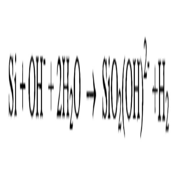
여기에서, SiO2(OH)2- 는 용해 가능한 착물이다.Here, SiO 2 (OH) 2- is a soluble complex.
도 5g에 있어서, 실리콘 이산화층(306)은 식각 공정에 의하여 제거된다. 매립 실리콘 이산화층(306)은 불산 용액을 이용하여 화학적으로 식각될 수 있다. 이러한 구성에 있어서, 고농도 도핑된 (110) 실리콘층(114B)은 식각 저지층으로 사용된다. 예를 들어, 실리콘 이산화층(306)은 실온에서 49 wt% 불산 용액을 이용하여 식각될 수 있다. 이러한 특정한 용액은 실리콘 이산화층(306)을 약 2.5 ㎛/분으로 식각할 수 있다. 층(306)을 제거하는 식각 공정은 하기의 화학식으로 도시될 수 있다.In FIG. 5G,

도 5h에 있어서, 도핑된 실리콘층(114B) 상에 금속 기판(118)이 형성된다. 일 실시예에 있어서, 금속 기판(118)은 전해 도금(electroplating)과 같은 모든 공정들, 및/또는 플라즈마 기상 증착(plasma vapor deposition, PVD), 화학기상증착 (CVD), 등과 같은 증착 공정을 이용하여 형성될 수 있다. 다른 실시예에 있어서, 금속 기판(118)은 도핑된 실리콘층(114B) 상에 전해 도금될 수 있다. 금속 기판(118)은 구리, 알루미늄, 또는 솔더와 같은 합금들, 등을 이용할 수 있는 모든 금속 또는 전도물을 포함할 수 있다.In FIG. 5H, a
도 5h에 있어서, 지지층(802)을 제거한다. 지지층(802)은 많은 다른 기술들을 이용하여 제거될 수 있다. 예를 들어, 지지층(802)은 극자외선 공정을 이용하여 제거될 수 있고, 이때에 부착 테이프는 소정의 기간 동안 충분한 양의 자외선에 노출되는 경우, 풀어지도록 구성된다. 결과적으로, 본 발명의 일부 실시예들에 따라서, 도 5h의 반도체 프로세스 구조(500)는 개개의 소자들(다이들)로 다이싱될 수 있다.In FIG. 5H, the
도 4a 내지 도 4f 및 도 5a 내지 도 5h과 관련하여 상술한 바와 같이, 본 발명은, 채널 저항을 감소시키기 위하여, <110> 방향으로 정공 전류 전도를 용이하게 하도록, (110) 배향 실리콘 물질 상에 p-채널 트렌치 MOSFET 소자를 제조하는 방법을 제공한다. 구체적인 실시예에 있어서, 이러한 유형의 웨이퍼들 상의 수직 트렌치들은 (110) 면들 상에 트렌치 바닥과 측벽을 모두 가지고, 상기 트렌치 최상측으로부터 상기 트렌치 바닥으로 흐르는(채널 방향) 전류의 방향은 <110> 방향이다. 상기 방법은 트렌치 게이트 MOSFET 또는 쉴디드 게이트 트렌치 MOSFET와 같은 수직 소자를 형성하기 위하여 사용될 수 있고, 수직 방향의 전류 전도를 강화한다. 예를 들어, 도 5h에 있어서, 전류가 금속층들(116, 118) 사이에 및 소자층(107)을 통하여 전도될 수 있고, 소자층(107)은 트렌치 게이트 MOSFET 또는 쉴디드 게이트 트렌치 MOSFET를 포함한다. 또한, 다른 실시예에 있어서, 소자층(107)은 다이오드들 또는 IGBT들과 같은 다른 수직 소자들을 포함할 수 있다.As described above with respect to FIGS. 4A-4F and 5A-5H, the present invention provides a method for (110) oriented silicon material phase to facilitate hole current conduction in the <110> direction to reduce channel resistance. A method of fabricating a p-channel trench MOSFET device is provided. In a specific embodiment, vertical trenches on this type of wafers have both trench bottoms and sidewalls on (110) faces, and the direction of current flowing from the top of the trench to the trench bottom (channel direction) is <110>. Direction. The method can be used to form vertical devices, such as trench gate MOSFETs or shielded gate trench MOSFETs, and enhance current conduction in the vertical direction. For example, in FIG. 5H, current can be conducted between the metal layers 116, 118 and through the
도 6은 본 발명의 다른 실시예에 따라서, 실리콘 기판의 식각 속도와 그의 붕소 농도와의 관계를 도시하는 개략도이다. 이 도면은 단지 예시적이며, 본 발명의 범위를 한정하는 것은 아니다. 본 기술 분야의 당업자들은 다른 변형들, 변화들, 또는 대체물들을 인식할 수 있다. 도시된 바와 같이, 붕소 농도가 약 1 x 1019 cm-3 이상으로 증가됨에 따라, 실리콘의 식각 속도는 급격하게 감소된다. 특히, KOH 또는 에틸렌디아민/피토카테콜/물(ehtylenediamine/ pytocatechol/water ,EDP)을 이용하여 고농도 및 저농도로 붕소 도핑된 실리콘 기판들 사이에 큰 식각 속도의 차이가 있다. 예를 들어, 81℃에서의 EDP 용액 내의 붕소 농도 < 1 x 1019 cm-3 이하의 붕소 농도(붕소 농도 < 1 x 1019 cm-3) 에서의 식각 속도는 약 20 ㎛/시간이고, 1 x 1020 cm-3의 붕소 농도에서는 식각 속도가 0.1 ㎛/시간이다. 상기 식각 속도의 차이는 200 배 이상일 수 있다. 유사한 식각 속도 차이는 KOH 화학물에서 발견된다. 이러한 식각 차이는 식각 저지층으로 상기 고농도 붕소 도핑된 도핑된 실리콘층을 사용할 수 있다. 저농도 도핑된 P-형 실리콘과 고농도 도핑된 P-형 실리콘 사이의 식각 선택비는 본 발명의 실시예의 방법에서 유용하게 이용될 수 있다.FIG. 6 is a schematic diagram showing a relationship between an etching rate of a silicon substrate and its boron concentration according to another embodiment of the present invention. FIG. This figure is illustrative only and does not limit the scope of the invention. Those skilled in the art can recognize other variations, changes, or substitutions. As shown, as the boron concentration is increased above about 1 × 10 19 cm −3 , the etching rate of silicon is drastically reduced. In particular, there is a large difference in etching rates between high and low boron doped silicon substrates using KOH or ethylenediamine / phytocatechol / water (EDP). For example, the etch rate in the boron concentration <1 x 10 19 cm -3 boron concentration below in EDP solution at 81 ℃ (boron concentration <1 x 10 19 cm -3) is about 20 ㎛ / hour, 1 At a boron concentration of x 10 20 cm -3 , the etching rate is 0.1 μm / hour. The difference in the etching rate may be 200 times or more. Similar etching rate differences are found in KOH chemicals. This etching difference may use the high boron doped silicon layer as an etch stop layer. Etch selectivity between lightly doped P-type silicon and heavily doped P-type silicon can be usefully employed in the method of embodiments of the present invention.
도 7a 내지 도 7g 본 발명의 다른 실시예에 따른, 고농도 도핑된 P-형 (110) 배향 기판을 이용하여 수직 소자를 형성하기 위한 다른 공정 흐름을 도시하는 개략적인 단면도들이다. 먼저, 도 7a에 있어서, 고농도 붕소 도핑된 도핑된 (110) 층(114) (농도 > 6 x 1019 cm-3를 가짐)이 (110) 배향 실리콘 웨이퍼(708) 상에 붕소 주입을 통하여 에피택셜하게 성장하거나 형성될 수 있다. 단지 예시적으로서, 에피 공정은 B2H6 도핑 종들(5000ppm의 농도에서 H2와 혼합됨)과 함께 1060℃ 에서 수행된다. 이를 대신하여, 고농도 도핑된 층(114)은 붕소 이온 주입에 의하여 형성될 수 있다. 주입은 고농도 도핑된 실리콘층을 생성하도록, 1/2시간 동안 1 x 1016 cm-2 의 도즈로 60 KeV일 수 있다. 이러한 공정을 완료한 후에, 도 7b에 도시된 바와 같이 원하는 소자 에피층(106)이 성장한다. 이어서, 상기 웨이퍼는 소자를 형성하기 위하여 소자 제조 공정을 거친다. 도 7c에 있어서, 소자층(107) 및 금속층(116)이 형성되고, 도 5a 내지 도 5h에 도시된 트렌치 게이트 MOSFET 또는 쉴디드 게이트 트렌치 MOSFET, 또는 다른 수직 소자들을 포함할 수 있다. 이어서 종료된 웨이퍼는 도 7d에 도시된 바와 같이, 지지 기판(802), 예를 들어, 유리 캐리어에 부착되고, 기판 이전을 대기한다.7A-7G are schematic cross-sectional views illustrating another process flow for forming a vertical device using a heavily doped P-type (110) oriented substrate, in accordance with another embodiment of the present invention. First, in FIG. 7A, a high concentration boron doped (110) layer 114 (having concentration> 6 × 10 19 cm −3 ) is epitaxially formed through boron implantation on a (110) oriented
도 7e에 있어서, 지지 기판 실리콘 웨이퍼(708)의 대부분(예를 들어, 90%)은 저농도 도핑된 (110) 배향 실리콘 웨이퍼(708A)의 일정한 두께, 예를 들어 5 ㎛의 두께가 남을 때까지 기계적 연마 및 화학적 식각을 통하여 제거된다. 최종 5 ㎛ 두께의 실리콘(708A)이 EDP 또는 KOH에 의하여 제거된다. EDP/KOH 식각의 높은 선택비 때문에, 실리콘 식각은 고농도 도핑된 붕소 실리콘(114)에서 정지된다. 도 7f에 있어서, 이러한 웨이퍼는 후측 금속 증착(118)을 위하여 준비되고, 유리 기판(802)의 제거에 의하여 이전되는 금속을 지지하고, 이에 따라 도 7g에 도시된 소자 구조를 형성한다. 상기 방법은, 도 5a 내지 도 5h과 관련되어 상술한 공정들과 유사하게, 수직 소자 제조, 지지층 부착, 금속 증착 등과 같은 공정들을 포함한다.In FIG. 7E, most of the support substrate silicon wafer 708 (eg, 90%) remains until a constant thickness of the lightly doped (110) oriented
따라서, 도 7a 내지 도 7g는 개선된 정공 이동도를 위한 (110) P-형 실리콘 내에 수직 소자를 형성하기 위한 다른 방법을 도시하고, 저항을 감소시키기 위하여 고농도 도핑된 (110) P-형 드레인 영역들 및 금속층들을 또한 제공한다. 도시된 바와 같이, 공정은 고농도 도핑된 P-형 실리콘과 저농도 도핑된 P-형 실리콘 사이에 식각 선택비에 의하여 단순화된다.Thus, FIGS. 7A-7G illustrate another method for forming vertical devices in (110) P-type silicon for improved hole mobility, and heavily doped (110) P-type drains to reduce resistance. Areas and metal layers are also provided. As shown, the process is simplified by etch selectivity between heavily doped P-type silicon and lightly doped P-type silicon.
전력 트렌치 MOSFET 소자들을 위한 (110)/<110> 구성된 웨이퍼들을 적용하는 다른 시도는 (110) 면 상에 고품질 게이트 산화층을 형성하는 것이다. 주요한 점은 원하는 문턱 전압 및 문턱 전압 안정성을 구현하기 위하여, 고정된 산화층 전하와 계면 트랩 밀도(Dit) 모두를 감소시키는 것이다. 계면 트랩 밀도(Dit)는 표면 상에 가능한 결합들의 밀도에 비례한다. 표 1은 다른 결정학적 평면들의 실리콘 특성들을 정리되어 있다. (100) 면 및 (111) 면에서의 계면 트랩 밀도(Dit)들은 각각 2 x 10¹⁰ 및 2 x 10¹¹ l/cm2-eV이다. (110) 면 상의 단위 면적당 가능한 결합들은 (100) 면과 (111) 면 사이에 있고, 이에 따라 (110) 면의 계면 트랩 밀도(Dit)는, 비록 데이터가 제공되지 않지만, 2 x 10¹⁰ l/cm2-eV 및 2 x 10¹¹ l/cm2-eV 사이에 있다. 본 발명의 실시예들에 따라서, 산화층 성장 속도를 감소시키고 및 추가적인 수소 어닐링을 추가하는 것은 계면 트랩 밀도(Dit) 및 고정된 산화층 전하를 더 감소시킬 수 있고, 게이트 산화층 집적을 증가시킬 수 있다.Another attempt to apply (110) / <110> configured wafers for power trench MOSFET devices is to form a high quality gate oxide layer on the (110) plane. The main point is to reduce both the fixed oxide charge and the interface trap density (D it ) to achieve the desired threshold voltage and threshold voltage stability. The interface trap density D it is proportional to the density of possible bonds on the surface. Table 1 summarizes the silicon properties of the different crystallographic planes. The interfacial trap densities (D it ) at the (100) and (111) planes are 2 x 10 10 and 2 x 10 11 l / cm 2 -eV, respectively. Possible bonds per unit area on the (110) plane are between the (100) plane and the (111) plane, so that the interface trap density (D it ) of the (110) plane is 2 x 10 10 , although no data is provided. between l / cm 2 -eV and 2 x 10 11 l / cm 2 -eV. In accordance with embodiments of the present invention, reducing the oxide layer growth rate and adding additional hydrogen annealing can further reduce the interface trap density (D it ) and the fixed oxide layer charge and increase the gate oxide layer integration. .
이상과 같이, 본 발명의 특정한 실시예들에 대하여 설명하였다고 하여도, 다양한 변형들, 변화들, 치환들이 가능할 수 있다. 예를 들어, 본 발명이 수직 MOSFET들을 도시하고 있다고 하여도, 본 발명은 도 1 및 도 2에 도시된 구조들로부터 기판의 극성을 단지 반대로 함으로써 트렌치 게이트 IGBT들과 같은 다른 구조들에 용이하게 적용될 수 있다. 또한, 본 발명은 트렌치 게이트 구조들에 한정되는 것은 아니고, 본 발명은 평면형 게이트 수직 MOSFET들, 평면형 게이트 수직 IGBT들, 다이오들, 및 다양한 유형의 사이리스터들(thyristors)과 같은 다른 소자들을 형성하기 위하여 사용될 수 있다. 따라서, 본 발명의 기술적 사상의 범위는 설명된 실시예들에 한정되는 것은 아니고, 하기의 청구항에 의하여 한정된다.As described above, although specific embodiments of the present invention have been described, various modifications, changes, and substitutions may be possible. For example, even though the present invention shows vertical MOSFETs, the present invention is easily applied to other structures such as trench gate IGBTs by simply inverting the polarity of the substrate from the structures shown in FIGS. 1 and 2. Can be. In addition, the present invention is not limited to trench gate structures, and the present invention is directed to forming other devices such as planar gate vertical MOSFETs, planar gate vertical IGBTs, diodes, and various types of thyristors. Can be used. Therefore, the technical scope of the present invention is not limited to the described embodiments, but is defined by the following claims.
100: P-형 트렌치 게이트 MOSFET, 102: 트렌치들, 104: N-웰 바디 영역
106: P-형 드리프트 또는 에피택셜 영역, 107: 반도체 구조층
108: 유전층들, 110: 도전 물질, 112: P-형 소스 영역들,
114: P-형 고농도 도핑된 실리콘층, 116: 금속 소스층
117: N+ 바디 영역, 118: 금속 기판
200: P-형 쉴디드 게이트 트렌치 MOSFET
202: 트렌치들, 204: N-웰 바디 영역
206: P-형 드리프트 또는 에피택셜 영역, 207: 반도체 구조층
208: 유전층들, 210: 도전 물질, 212: P-형 소스 영역들,
214: P-형 고농도 도핑된 실리콘층, 216: 금속 소스층
217: N+ 바디 영역, 218: 금속 기판
G: 게이트 전극, D: 드레인 터미널100: P-type trench gate MOSFET, 102: trenches, 104: N-well body region
106: P-type drift or epitaxial region, 107: semiconductor structure layer
108: dielectric layers, 110: conductive material, 112: P-type source regions,
114: P-type heavily doped silicon layer, 116: metal source layer
117: N + body region, 118: metal substrate
200: P-type shielded gate trench MOSFET
202 trenches, 204 N-well body region
206: P-type drift or epitaxial region, 207: semiconductor structure layer
208: dielectric layers, 210: conductive material, 212: P-type source regions,
214: P-type heavily doped silicon layer, 216: metal source layer
217: N + body region, 218: metal substrate
G: gate electrode, D: drain terminal
Claims (52)
(110)의 표면 결정 배향 및 제1 전도도에 의하여 특성화되고, 고농도 도핑된 제1 P-형 반도체층을 제공하는 단계;
상기 제1 P-형 반도체층 상에 (110)의 표면 결정 배향을 가지고, 상기 제1 전도도에 비하여 낮은 전도도에 의하여 특성화된 제2 P-형 반도체층을 형성하는 단계;
상기 제2 P-형 반도체층 상에 최상 도전층을 형성하는 단계; 및
상기 제1 P-형 반도체층 하측에 바닥 도전층을 형성하는 단계;
를 포함하고,
상기 최상 도전층으로부터 상기 제2 P-형 반도체층을 통하여 상기 바닥 도전층까지의 전류 전도는, (110) 결정면 상에서 <110> 결정 배향을 따르는 정공 이동도에 의하여 특성화된 것을 특징으로 하는 반도체 소자 형성방법.A method of forming a semiconductor device on a heavily doped P-type (110) semiconductor layer on a metal substrate, the method comprising:
Providing a heavily doped first P-type semiconductor layer characterized by a surface crystal orientation and a first conductivity of (110);
Forming a second P-type semiconductor layer on the first P-type semiconductor layer, the second P-type semiconductor layer having a surface crystal orientation of (110) and characterized by low conductivity relative to the first conductivity;
Forming an uppermost conductive layer on the second P-type semiconductor layer; And
Forming a bottom conductive layer under the first P-type semiconductor layer;
Including,
The current conduction from the uppermost conductive layer to the bottom conductive layer through the second P-type semiconductor layer is characterized by hole mobility along a <110> crystallographic orientation on a (110) crystal plane. Formation method.
상기 제1 P-형 반도체층을 제공하는 단계는,
제1 지지 기판을 제공하는 단계; 및
상기 제1 지지 기판 상에 P-형 고농도 도핑된 (110) 실리콘층을 형성하는 단계;
를 포함하고,
상기 제1 지지 기판의 적어도 최상층은 상기 P-형 고농도 도핑된 (110) 실리콘층에 대한 선택적 식각 공정에 의하여 제거가능한 것을 특징으로 하는 반도체 소자 형성방법.The method of claim 1,
Providing the first P-type semiconductor layer,
Providing a first support substrate; And
Forming a P-type heavily doped (110) silicon layer on the first support substrate;
Including,
At least a top layer of the first support substrate is removable by a selective etching process on the P-type heavily doped (110) silicon layer.
상기 제1 지지 기판은 실리콘 기판 상의 산화물층을 포함하는 것을 특징으로 하는 반도체 소자 형성방법.The method of claim 2,
And the first support substrate comprises an oxide layer on a silicon substrate.
상기 P-형 고농도 도핑된 (110) 실리콘층을 형성하는 단계는,
(110) 결정 배향, P-형 전도도, 및 저농도 도핑에 의하여 특성화된 제1 실리콘 기판을 제공하는 단계;
상기 제1 실리콘 기판 상에 P-형 고농도 도핑된 (110) 실리콘층을 형성하는 단계;
상기 P-형 고농도 도핑된 (110) 실리콘층 상에 제1 산화물층을 형성하는 단계;
상측 (110) 층 및 하측 (110) 층을 형성하기 위하여, 상기 고농도 도핑된 (110) 실리콘층 내부에 수소에 의하여 충분히 약화된 영역을 형성하여 상기 약화된 영역을 따라서 상기 고농도 도핑된 (110) 실리콘층을 분리하도록, 상기 고농도 도핑된 (110) 실리콘층 내로 수소 이온들을 주입하는 단계;
상기 제1 기판을 상기 제1 지지 기판에 부착하는 단계; 및
상기 제1 지지 기판 상의 상기 제2 실리콘 이산화물층에 부착된 상기 하측 (110) 층이 잔류하도록, 상기 약화된 영역을 따라서 상기 P-형 고농도 도핑된 (110) 실리콘층을 분리하는 단계;
를 포함하는 것을 특징으로 하는 반도체 소자 형성방법.The method of claim 3, wherein
Forming the P-type heavily doped (110) silicon layer,
Providing a first silicon substrate characterized by (110) crystal orientation, P-type conductivity, and low concentration doping;
Forming a P-type heavily doped (110) silicon layer on the first silicon substrate;
Forming a first oxide layer on the P-type heavily doped (110) silicon layer;
To form an upper (110) layer and a lower (110) layer, a region sufficiently weakened by hydrogen is formed inside the heavily doped (110) silicon layer to form the heavily doped (110) along the weakened region. Implanting hydrogen ions into the heavily doped (110) silicon layer to separate the silicon layer;
Attaching the first substrate to the first support substrate; And
Separating the P-type heavily doped (110) silicon layer along the weakened region so that the lower (110) layer attached to the second silicon dioxide layer on the first support substrate remains;
Method of forming a semiconductor device comprising a.
상기 제1 지지 기판을 제거하는 단계는,
실리콘 기판을 연마하는 단계;
식각 저지층(etch stop)으로 상기 산화물층을 이용하여 잔류한 상기 실리콘 기판을 식각하는 단계; 및
식각 저지층으로 상기 P-형 고농도 도핑된 (110) 실리콘층을 이용하여 상기 산화물층을 식각하는 단계;
를 포함하는 것을 특징으로 하는 반도체 소자 형성방법.The method of claim 3, wherein
Removing the first support substrate,
Polishing the silicon substrate;
Etching the remaining silicon substrate using the oxide layer as an etch stop; And
Etching the oxide layer using the P-type heavily doped (110) silicon layer as an etch stop layer;
Method of forming a semiconductor device comprising a.
상기 제1 지지 기판은, (110) 결정 배향, P-형 전도도, 및 저농도 도핑(light doping)에 의하여 특성화된 실리콘 기판을 포함하는 것을 특징으로 하는 반도체 소자 형성방법.The method of claim 2,
Wherein the first support substrate comprises a silicon substrate characterized by (110) crystal orientation, P-type conductivity, and light doping.
상기 P-형 고농도 도핑된 (110) 실리콘층을 형성하는 단계는,
인-싯츄(in-situ) 도핑을 포함하는 에피택셜 공정을 이용하는 단계를 포함하는 것을 특징으로 하는 반도체 소자 형성방법.The method according to claim 6,
Forming the P-type heavily doped (110) silicon layer,
A method of forming a semiconductor device, comprising using an epitaxial process comprising in-situ doping.
상기 P-형 고농도 도핑된 (110) 실리콘층을 형성하는 단계는,
이온 주입 공정을 이용하는 단계를 포함하는 것을 특징으로 하는 반도체 소자 형성방법.The method according to claim 6,
Forming the P-type heavily doped (110) silicon layer,
A method of forming a semiconductor device comprising the step of using an ion implantation process.
상기 제1 지지 기판을 제거하는 단계는,
식각 저지층으로 상기 고농도 도핑된 P-형 실리콘층을 이용하여 상기 실리콘 기판을 제거하는 단계를 포함하는 것을 특징으로 하는 반도체 소자 형성방법.The method according to claim 6,
Removing the first support substrate,
And removing the silicon substrate using the heavily doped P-type silicon layer as an etch stop layer.
상기 제1 지지 기판을 제거하는 단계는,
KOH 또는 EDP를 포함하는 습식 식각 공정을 이용하여 상기 실리콘 기판을 식각하는 단계를 포함하는 것을 특징으로 하는 반도체 소자 형성방법.The method according to claim 6,
Removing the first support substrate,
Etching the silicon substrate using a wet etching process comprising KOH or EDP.
상기 P-형 고농도 도핑된 (110) 실리콘 층 및 상기 제2 P-형 반도체층 내에 및 그 상에, (110) 면 상에서 <110> 방향으로의 전류 전도에 의하여 특성화된 수직 반도체 소자 구조를 형성하는 단계;
상기 최상 금속층에 제2 지지 기판을 부착하는 단계; 및
상기 P-형 고농도 도핑된 (110) 실리콘층의 표면을 노출하도록 상기 제1 지지 기판을 제거하는 단계;
를 더 포함하고,
상기 제1 지지 기판의 적어도 최상 층은 상기 P-형 고농도 도핑된 (110) 실리콘층에 대하여 선택적 식각 공정을 이용하여 제거되는 것을 특징으로 하는 반도체 소자 형성방법.The method of claim 2,
Forming a vertical semiconductor device structure characterized by current conduction in the <110> direction on the (110) plane in and on the P-type heavily doped (110) silicon layer and the second P-type semiconductor layer Making;
Attaching a second support substrate to the uppermost metal layer; And
Removing the first support substrate to expose a surface of the P-type heavily doped (110) silicon layer;
Further comprising:
At least a top layer of the first support substrate is removed using a selective etching process with respect to the P-type heavily doped (110) silicon layer.
상기 수직 반도체 소자 구조를 형성하는 단계는,
P-형 고농도 도핑된 (110) 실리콘층 상에 저농도 도핑된 (110) 에피택셜층을 형성하는 단계; 및
상기 에피택셜층 내에 및 그 상에 트렌치 구조를 형성하는 단계;
를 포함하는 것을 특징으로 하는 반도체 소자 형성방법.The method of claim 11,
Forming the vertical semiconductor device structure,
Forming a lightly doped (110) epitaxial layer on the P-type heavily doped (110) silicon layer; And
Forming a trench structure in and on the epitaxial layer;
Method of forming a semiconductor device comprising a.
(110)의 결정 배향, P-형 전도도, 및 저농도 도핑에 의하여 에 의하여 특성화된 제1 실리콘 기판을 제공하는 단계;
상기 제1 실리콘 기판 상에 P-형 고농도 도핑된 (110) 실리콘층을 형성하는 단계;
상기 P-형 고농도 도핑된 (110) 실리콘층의 부분을 상측 산화물층을 포함하는 제2 실리콘 기판에 이전하는 단계;
상기 고농도 도핑된 (110) 층의 이전된 부분 내에 및 그 상에, (110) 면 상에서 <110> 방향으로의 전류 전도에 의하여 특성화되고, 최상 금속층을 가지는 수직 반도체 소자 구조를 형성하는 단계;
상기 최상 금속층에 지지 기판을 부착하는 단계;
상기 제2 실리콘 기판을 제거하는 단계;
상기 수직 반도체 소자 구조 하에 금속 기판으로서 충분한 두께를 갖는 바닥 금속층을 제공하는 단계; 및
상기 지지 기판을 제거하는 단계;를 포함하는 것을 특징으로 하는 반도체 소자 형성방법.A method of forming a semiconductor device on a heavily doped P-type (110) semiconductor layer on a metal substrate, the method comprising:
Providing a first silicon substrate characterized by a crystal orientation, P-type conductivity, and low concentration doping of (110);
Forming a P-type heavily doped (110) silicon layer on the first silicon substrate;
Transferring a portion of the P-type heavily doped (110) silicon layer to a second silicon substrate comprising an upper oxide layer;
Forming a vertical semiconductor device structure characterized by current conduction in a <110> direction on a (110) plane, in and on a transferred portion of the heavily doped (110) layer, the top metal layer;
Attaching a support substrate to the top metal layer;
Removing the second silicon substrate;
Providing a bottom metal layer having a sufficient thickness as a metal substrate under the vertical semiconductor device structure; And
Removing the support substrate;
상기 P-형 고농도 도핑된 (110) 실리콘층을 형성하는 단계는,
에피택셜 공정 또는 이온 주입 공정을 이용하는 단계를 포함하는 것을 특징으로 하는 반도체 소자 형성방법.The method of claim 13,
Forming the P-type heavily doped (110) silicon layer,
A method of forming a semiconductor device comprising the step of using an epitaxial process or an ion implantation process.
상기 고농도 도핑된 실리콘층의 부분을 이전하는 단계는,
상기 P-형 고농도 도핑된 (110) 실리콘층 상에 실리콘 산화물층을 형성하는 단계;
상측 (110) 층 및 하측 (110) 층을 형성하기 위하여, 상기 고농도 도핑된 (110) 실리콘층 내부에 수소에 의하여 충분히 약화된 영역을 형성하여 상기 약화된 영역을 따라서 고농도 도핑된 (110) 실리콘층을 분리하도록, 상기 고농도 도핑된 (110) 실리콘층 내로 수소 이온들을 주입하는 단계;
제2 실리콘 기판을 제공하는 단계;
상기 제1 실리콘 기판을 상기 제2 실리콘 기판에 부착하는 단계; 및
상기 제2 실리콘 기판의 상의 상기 산화물층에 부착되고 P-형 전도도 및 고농도 도핑에 의하여 특성화된 상기 하측 (110) 층이 잔류하도록, 상기 약화된 영역을 따라서 상기 P-형 고농도 도핑된 (110) 실리콘층을 분리하는 단계;
를 포함하는 것을 특징으로 하는 반도체 소자 형성방법.The method of claim 13,
The step of transferring the portion of the heavily doped silicon layer,
Forming a silicon oxide layer on the P-type heavily doped (110) silicon layer;
To form an upper (110) layer and a lower (110) layer, a heavily doped (110) silicon is formed along the weakened region by forming a region sufficiently weakened by hydrogen within the heavily doped (110) silicon layer. Implanting hydrogen ions into the heavily doped (110) silicon layer to separate the layers;
Providing a second silicon substrate;
Attaching the first silicon substrate to the second silicon substrate; And
The P-type heavily doped 110 along the weakened region such that the lower 110 layer adheres to the oxide layer on the second silicon substrate and is characterized by P-type conductivity and high concentration doping. Separating the silicon layer;
Method of forming a semiconductor device comprising a.
수소 이온들을 주입하는 단계는,
약 170 KeV의 주입 에너지로 수소 이온들을 주입하는 단계를 포함하는 것을 특징으로 하는 반도체 소자 형성방법.The method of claim 15,
Injecting hydrogen ions,
Implanting hydrogen ions at an implantation energy of about 170 KeV.
상기 P-형 고농도 도핑된 (110) 실리콘층을 분리하는 단계는,
상기 상측 (110) 층 및 상기 하측 (110) 층을 분리하도록 상기 영역을 충분히 어닐링하는 단계를 포함하는 것을 특징으로 하는 반도체 소자 형성방법.The method of claim 15,
Separating the P-type heavily doped (110) silicon layer,
And annealing the region sufficiently to separate the upper (110) layer and the lower (110) layer.
상기 영역을 어닐링하는 단계는,
약 5 시간 내지 10 시간 범위의 시간 동안 약 150℃ 내지 300℃ 범위의 온도로 상기 영역을 가열하는 단계를 포함하는 것을 특징으로 하는 반도체 소자 형성방법.The method of claim 17,
Annealing the region,
Heating the region to a temperature in a range from about 150 ° C. to 300 ° C. for a time in a range from about 5 hours to 10 hours.
상기 영역을 어닐링하는 단계는,
약 15 분 동안 약 450℃의 온도로 상기 영역을 가열하는 단계를 포함하는 것을 특징으로 하는 반도체 소자 형성방법.The method of claim 17,
Annealing the region,
Heating the region at a temperature of about 450 ° C. for about 15 minutes.
상기 제2 실리콘 기판을 제거하는 단계는,
상기 제2 실리콘 기판을 소정의 두께로 연마하는 단계를 포함하는 것을 특징으로 하는 반도체 소자 형성방법.The method of claim 13,
Removing the second silicon substrate,
And polishing the second silicon substrate to a predetermined thickness.
상기 제2 실리콘 기판은 (100) 결정 배향에 의하여 특성화된 것을 특징으로 하는 반도체 소자 형성방법.The method of claim 13,
And wherein said second silicon substrate is characterized by a (100) crystal orientation.
수직 반도체 소자 구조를 형성하는 단계는,
상기 고농도 도핑된 (110) 층의 이전된 부분 상에 저농도 도핑된(110) 에피택셜층을 형성하는 단계; 및
상기 저농도 도핑된 (110) 에피택셜층 내에 및 그 상에 수직 소자를 형성하는 단계;
를 포함하는 것을 특징으로 하는 반도체 소자 형성방법.The method of claim 13,
Forming the vertical semiconductor device structure,
Forming a lightly doped epitaxial layer on the transferred portion of the heavily doped (110) layer; And
Forming a vertical element in and on the lightly doped (110) epitaxial layer;
Method of forming a semiconductor device comprising a.
상기 제2 실리콘 기판을 제거하는 단계는,
상기 상측 산화물층으로부터 상기 제2 실리콘 기판을 선택적으로 화학적 식각하는 단계를 포함하는 것을 특징으로 하는 반도체 소자 형성방법.The method of claim 13,
Removing the second silicon substrate,
Selectively chemically etching the second silicon substrate from the upper oxide layer.
상기 바닥 금속층을 제공하는 단계는,
상기 금속층을 상기 도핑된 실리콘층에 전해 도금(electroplating)하는 단계를 포함하는 것을 특징으로 하는 반도체 소자 형성방법.The method of claim 13,
Providing the bottom metal layer,
Electroplating the metal layer on the doped silicon layer.
상기 바닥 금속층은 구리를 포함하는 것을 특징으로 하는 반도체 소자 형성방법.The method of claim 24,
And the bottom metal layer comprises copper.
(110) 결정 배향, P-형 전도도, 및 저농도 도핑에 의하여 특성화된 제1 실리콘 기판을 제공하는 단계;
상기 제1 실리콘 기판 상에 P-형 고농도 도핑된 (110) 실리콘층을 형성하는 단계;
상기 P-형 고농도 도핑된 (110) 실리콘층 상에 제1 산화물층을 형성하는 단계;
상측 (110) 층 및 하측 (110) 층을 형성하기 위하여, 상기 고농도 도핑된 (110) 실리콘층 내부에 수소에 의하여 충분히 약화된 영역을 형성하여 상기 약화된 영역을 따라서 상기 고농도 도핑된 (110) 실리콘층을 분리하도록, 상기 고농도 도핑된 (110) 실리콘층 내로 수소 이온들을 주입하는 단계;
(100) 결정 배향에 의하여 특성화된 제2 실리콘 기판을 제공하는 단계;
상기 제1 산화물층이 상기 제2 실리콘 기판에 점착적으로(adhesively) 부착되도록, 상기 제1 기판을 상기 제2 실리콘 기판에 부착하는 단계; 및
상기 제2 실리콘 기판 상의 상기 제2 실리콘 이산화물층에 부착되고 P-형 전도도 및 고농도 도핑에 의하여 특성화된 상기 하측 (110) 층이 잔류하도록, 상기 약화된 영역을 따라서 상기 P-형 고농도 도핑된 (110) 실리콘층을 분리하는 단계;
를 포함하는 실리콘층 형성방법.A method of forming a heavily doped P-type (110) silicon layer on a (100) silicon substrate, the forming method comprising:
Providing a first silicon substrate characterized by (110) crystal orientation, P-type conductivity, and low concentration doping;
Forming a P-type heavily doped (110) silicon layer on the first silicon substrate;
Forming a first oxide layer on the P-type heavily doped (110) silicon layer;
To form an upper (110) layer and a lower (110) layer, a region sufficiently weakened by hydrogen is formed inside the heavily doped (110) silicon layer to form the heavily doped (110) along the weakened region. Implanting hydrogen ions into the heavily doped (110) silicon layer to separate the silicon layer;
Providing a second silicon substrate characterized by (100) crystal orientation;
Attaching the first substrate to the second silicon substrate such that the first oxide layer is adhesively attached to the second silicon substrate; And
The P-type heavily doped along the weakened region so that the lower 110 layer adheres to the second silicon dioxide layer on the second silicon substrate and is characterized by P-type conductivity and high concentration doping ( 110) separating the silicon layer;
Silicon layer forming method comprising a.
상기 제2 실리콘 기판은 상측 산화물층을 더 포함하는 것을 특징으로 하는 실리콘층 형성방법.The method of claim 26,
And the second silicon substrate further comprises an upper oxide layer.
(110) 결정 배향, P-형 전도도, 및 저농도 도핑에 의하여 특성화된 제1 실리콘 기판을 제공하는 단계;
상기 제1 실리콘 기판 상에 P-형 고농도 도핑된 (110) 실리콘층을 형성하는 단계;
P-형 고농도 도핑된 (110) 실리콘층 내에 및 그 상에, (110) 면 상에서 <110> 방향으로의 전류 전도에 의하여 특성화되고 최상 금속층을 포함하는 수직 반도체 소자 구조를 형성하는 단계;
지지 기판을 상기 최상 금속층에 부착하는 단계;
식각 저지층으로 상기 P-형 고농도 도핑된 (110) 실리콘층을 이용하여 상기 제1 실리콘 기판을 제거하는 단계;
상기 P-형 고농도 도핑된 (110) 실리콘층의 표면을 노출하는 단계;
상기 P-형 고농도 도핑된 (110) 실리콘층의 표면과 접촉하는 금속층을 제공하는 단계; 및
상기 지지 기판을 제거하는 단계;
를 포함하는 것을 특징으로 하는 반도체 구조 형성방법.A method of forming P-type (110) semiconductor structures on a metal substrate, the method of forming
Providing a first silicon substrate characterized by (110) crystal orientation, P-type conductivity, and low concentration doping;
Forming a P-type heavily doped (110) silicon layer on the first silicon substrate;
Forming a vertical semiconductor device structure in and on the P-type heavily doped (110) silicon layer, characterized by current conduction in the <110> direction on the (110) plane and comprising a top metal layer;
Attaching a support substrate to the uppermost metal layer;
Removing the first silicon substrate using the P-type heavily doped (110) silicon layer as an etch stop layer;
Exposing a surface of said P-type heavily doped (110) silicon layer;
Providing a metal layer in contact with the surface of the P-type heavily doped (110) silicon layer; And
Removing the support substrate;
Method of forming a semiconductor structure comprising a.
상기 P-형 고농도 도핑된 (110) 실리콘층을 형성하는 단계는,
에피택셜 공정 또는 이온 주입 공정을 이용하는 단계를 포함하는 것을 특징으로 하는 반도체 구조 형성방법.29. The method of claim 28,
Forming the P-type heavily doped (110) silicon layer,
A method of forming a semiconductor structure, comprising using an epitaxial process or an ion implantation process.
상기 제1 실리콘 기판을 제거하는 단계는, KOH 또는 EDP를 포함하는 습식 식각 공정을 이용하여 상기 실리콘 기판을 제거하는 단계를 포함하는 것을 특징으로 하는 반도체 구조 형성방법.29. The method of claim 28,
The removing of the first silicon substrate may include removing the silicon substrate by using a wet etching process including KOH or EDP.
상기 수직 반도체 소자 구조들을 형성하는 단계는,
상기 하측 (110) 층 상에 저농도 도핑된 (110) 에피택셜층을 형성하는 단계; 및
상기 에피택셜층 내에 및 그 상에 수직 소자 구조를 형성하는 단계;를 포함하는 것을 특징으로 하는 반도체 구조 형성방법.29. The method of claim 28,
Forming the vertical semiconductor device structures,
Forming a lightly doped (110) epitaxial layer on the bottom (110) layer; And
Forming a vertical element structure in and on the epitaxial layer.
상기 바닥 금속층 상에 위치하고, (110)의 표면 결정 배향 및 제1 전도도에 의하여 특성화되고, 고농도 도핑된 제1 P-형 반도체층;
상기 제1 P-형 반도체층 상에 위치하고, (110)의 표면 결정 배향을 가지고, 상기 제1 전도도에 비하여 낮은 전도도에 의하여 특성화된 제2 P-형 반도체층; 및
상기 제2 P-형 반도체층 상에 위치한 최상 금속층;
을 포함하고,
상기 최상 금속층으로부터 상기 제2 P-형 반도체층을 통하여 상기 바닥 금속층까지의 전류 전도는, (110) 결정면 상에서 <110> 결정 배향을 따르는 정공 이동도에 의하는 것을 특징으로 하는 수직 반도체 소자.Bottom metal layer;
A heavily doped first P-type semiconductor layer positioned on the bottom metal layer and characterized by a surface crystal orientation and a first conductivity of (110);
A second P-type semiconductor layer located on the first P-type semiconductor layer, having a surface crystal orientation of (110), characterized by a lower conductivity than the first conductivity; And
An uppermost metal layer located on the second P-type semiconductor layer;
Including,
And wherein the current conduction from the uppermost metal layer to the bottom metal layer through the second P-type semiconductor layer is due to hole mobility along a <110> crystal orientation on the (110) crystal plane.
상기 제1 P-형 반도체층은 1 x 1017 cm-3 또는 그 이상의 도핑 농도를 가지는 것을 특징으로 하는 수직 반도체 소자.33. The method of claim 32,
Wherein the first P-type semiconductor layer has a doping concentration of 1 × 10 17 cm −3 or more.
상기 제1 P-형 반도체층은 6 x 1019 cm-3 보다 높은 도핑 농도를 가지는 것을 특징으로 하는 수직 반도체 소자.33. The method of claim 32,
And the first P-type semiconductor layer has a doping concentration higher than 6 x 10 19 cm -3 .
상기 제1 P-형 반도체층의 두께는 약 0.5 ㎛ 내지 약 3 ㎛ 범위인 것을 특징으로 하는 수직 반도체 소자.33. The method of claim 32,
Wherein the thickness of the first P-type semiconductor layer is in a range from about 0.5 μm to about 3 μm.
상기 제1 및 제2 P-형 반도체층들 각각은 에피택셜층인 것을 특징으로 하는 수직 반도체 소자.33. The method of claim 32,
And each of the first and second P-type semiconductor layers is an epitaxial layer.
상기 바닥 금속층은 상기 수직 반도체 소자를 지지하기 위한 충분한 두께를 가지는 것을 특징으로 하는 수직 반도체 소자.33. The method of claim 32,
And wherein the bottom metal layer has a sufficient thickness to support the vertical semiconductor device.
상기 수직 반도체 소자는 트렌치 게이트 P-채널 MOSFET을 포함하고,
상기 트렌치 게이트 MOSFET은,
상기 제2 P-형 반도체 영역 내로 연장된 트렌치;
상기 트렌치의 측벽과 바닥을 라이닝하는 게이트 유전물;
상기 트렌치 내에서 상기 유전층 상의 게이트 전극;
상기 트렌치 내의 상기 게이트 전극의 각각의 측의 옆에 위치하는 P-형 소스 영역들;
P-형 드리프트(drift) 영역;
상기 드리프트 영역 상으로 연장된 N-형 바디(body) 영역; 및
상기 고농도 도핑된 제1 P-형 반도체층의 적어도 부분을 포함하는 P-형 드레인 영역;
을 포함하는 것을 특징으로 하는 수직 반도체 소자.33. The method of claim 32,
The vertical semiconductor device comprises a trench gate P-channel MOSFET,
The trench gate MOSFET,
A trench extending into the second P-type semiconductor region;
A gate dielectric lining the sidewalls and bottom of the trench;
A gate electrode on the dielectric layer in the trench;
P-type source regions located next to each side of the gate electrode in the trench;
P-type drift region;
An N-type body region extending over the drift region; And
A P-type drain region including at least a portion of the heavily doped first P-type semiconductor layer;
Vertical semiconductor device comprising a.
상기 수직 반도체 소자는 P-채널 쉴디드(shielded) 게이트 트렌치 MOSFET을 포함하고,
상기 쉴디드 게이트 트렌치 MOSFET은,
상기 제2 P-형 반도체층 내로 연장된 트렌치;
상기 트렌치의 측벽 및 바닥 표면을 라이닝하는 쉴드 유전물;
상기 트렌치의 하측 부분에 위치하고, 상기 쉴드 유전물에 의하여 상기 제2 반도체층으로부터 절연된 쉴드 전극;
상기 쉴드 전극 상에 위치한 전극간 유전층;
상기 트렌치 측벽의 상측 부분을 라이닝하는 게이트 유전층; 및
상기 트렌치의 상측 부분에 상기 전극간 유전층 위로 위치하고, 상기 게이트 유전층에 의하여 상기 제2 P-형 반도체층으로부터 절연된 게이트 전극;
을 더 포함하는 것을 특징으로 하는 수직 반도체 소자.33. The method of claim 32,
The vertical semiconductor device comprises a P-channel shielded gate trench MOSFET,
The shielded gate trench MOSFET,
A trench extending into the second P-type semiconductor layer;
A shield dielectric lining the sidewalls and bottom surface of the trench;
A shield electrode disposed under the trench and insulated from the second semiconductor layer by the shield dielectric material;
An inter-electrode dielectric layer disposed on the shield electrode;
A gate dielectric layer lining an upper portion of the trench sidewalls; And
A gate electrode positioned over the inter-electrode dielectric layer in an upper portion of the trench and insulated from the second P-type semiconductor layer by the gate dielectric layer;
Vertical semiconductor device further comprises.
상기 제2 P-형 반도체층은,
P-형 드리프트(drift) 영역;
상기 드리프트 영역 상으로 연장된 N-형 바디 영역; 및
상기 바디 영역 내에 상기 트렌치에 인접하여 위치한 P-형 소스 영역들;
을 포함하는 것을 특징으로 하는 수직 반도체 소자.The method of claim 39,
The second P-type semiconductor layer,
P-type drift region;
An N-type body region extending onto the drift region; And
P-type source regions located adjacent to the trench in the body region;
Vertical semiconductor device comprising a.
바닥 금속층;
상기 바닥 금속층 상에 위치하고, (110)의 표면 결정 배향 및 제1 전도도에 의하여 특성화되고, 고농도 도핑된 제1 P-형 반도체층;
상기 제1 P-형 반도체층 상에 위치하고, (110)의 표면 결정 배향을 가지고 상기 제1 전도도에 비하여 낮은 전도도에 의하여 특성화된 제2 P-형 반도체층; 및
상기 제2 P-형 반도체층 내에 위치하는 N-형 바디 영역;
상기 바디 영역을 통하고, 상기 바디 영역의 하측에 위치한 상기 제2 P-형 반도체층의 바닥 부분 내로 연장되는 트렌치;
상기 트렌치의 측벽과 바닥을 라이닝하는 게이트 유전층;
상기 트렌치 내에 상기 게이트 유전층 상의 게이트 전극;
상기 트렌치 내의 상기 게이트 전극의 각각의 측의 옆에 위치하는 P-형 소스 영역들; 및
상기 제2 P-형 반도체층 상에 위치하고, 상기 소스 영역들 및 상기 바디 영역에 커플링된 최상 금속층;
을 포함하고,
상기 최상 금속층으로부터 상기 제2 P-형 반도체층을 통하여 상기 바닥 금속층까지의 전류 전도는 <110> 결정 배향을 따르는 정공 이동도에 의하여 특성화된 것을 특징으로 하는 수직 트렌치 게이트 MOSFET 소자.A vertical trench gate MOSFET semiconductor device formed in a (110) substrate,
Bottom metal layer;
A heavily doped first P-type semiconductor layer positioned on the bottom metal layer and characterized by a surface crystal orientation and a first conductivity of (110);
A second P-type semiconductor layer positioned on the first P-type semiconductor layer and characterized by a low conductivity relative to the first conductivity with a surface crystal orientation of (110); And
An N-type body region located in the second P-type semiconductor layer;
A trench extending through the body region and into a bottom portion of the second P-type semiconductor layer located below the body region;
A gate dielectric layer lining the sidewalls and bottom of the trench;
A gate electrode on the gate dielectric layer in the trench;
P-type source regions located next to each side of the gate electrode in the trench; And
An uppermost metal layer on the second P-type semiconductor layer and coupled to the source regions and the body region;
Including,
And wherein the current conduction from the top metal layer through the second P-type semiconductor layer to the bottom metal layer is characterized by hole mobility along a <110> crystal orientation.
상기 제1 P-형 반도체층은 1 x 1017 cm-3 또는 그 이상의 도핑 농도를 가지는 것을 특징으로 하는 수직 반도체 소자.42. The method of claim 41 wherein
Wherein the first P-type semiconductor layer has a doping concentration of 1 × 10 17 cm −3 or more.
상기 제1 P-형 반도체층은 6 x 1019 cm-3 보다 높은 도핑 농도를 가지는 것을 특징으로 하는 수직 반도체 소자.42. The method of claim 41 wherein
And the first P-type semiconductor layer has a doping concentration higher than 6 x 10 19 cm -3 .
상기 제1 P-형 반도체층의 두께는 약 0.5 ㎛ 내지 약 3 ㎛ 범위인 것을 특징으로 하는 수직 반도체 소자.42. The method of claim 41 wherein
Wherein the thickness of the first P-type semiconductor layer is in a range from about 0.5 μm to about 3 μm.
상기 제1 및 제2 P-형 반도체층들 각각은 에피택셜층인 것을 특징으로 하는 수직 반도체 소자.42. The method of claim 41 wherein
And each of the first and second P-type semiconductor layers is an epitaxial layer.
상기 바닥 금속층은 상기 수직 반도체 소자를 지지하기 위한 충분한 두께를 가지는 것을 특징으로 하는 수직 반도체 소자.42. The method of claim 41 wherein
And wherein the bottom metal layer has a sufficient thickness to support the vertical semiconductor device.
바닥 금속층;
상기 바닥 금속층 상에 위치하고, (110)의 표면 결정 배향 및 제1 전도도에 의하여 특성화되고, 고농도 도핑된 제1 P-형 반도체층;
상기 제1 P-형 반도체층 상에 위치하고, (110)의 표면 결정 배향을 가지고, 상기 제1 전도도에 비하여 낮은 전도도에 의하여 특성화된 제2 P-형 반도체층; 및
상기 제2 P-형 반도체층 내에 위치하는 N-형 바디 영역;
상기 바디 영역을 통하고, 상기 바디 영역의 하측에 위치한 상기 제2 P-형 반도체층의 바닥 부분 내로 연장되는 트렌치;
제1 쉴드 산화물층을 포함하고, 상기 트렌치의 측벽과 바닥 표면을 라이닝하 는 쉴드 유전층;
상기 트렌치의 하측 부분에 위치하고 상기 쉴드 유전층에 의하여 상기 반도체 영역으로부터 절연된 쉴드 전극;
상기 쉴드 전극 상에 위치한 전극간 유전층;
상기 트렌치 측벽의 상측 부분들을 라이닝하는 게이트 유전층;
상기 전극간 유전층 상의 상기 트렌치의 상측 부분에 위치하고, 상기 게이트 유전층에 의하여 상기 반도체 영역으로부터 절연된 게이트 전극;
상기 트렌치 내의 상기 게이트 전극의 각각의 측의 옆에 위치하는 P-형 소스 영역들; 및
상기 제2 P-형 반도체층 상에 위치하고, 상기 소스 영역들 및 상기 바디 영역에 커플링된 최상 금속층;
을 포함하고,
상기 최상 금속층으로부터 상기 제2 P-형 반도체층을 통하여 상기 바닥 금속층까지의 전류 전도는 (110) 결정 평면 상에서 <110> 결정 배향을 따르는 정공 이동도에 의하여 특성화된 것을 특징으로 하는 수직 쉴디드 게이트 트렌치 MOSFET 반도체 소자.A vertical shielded gate trench MOSFET element formed in a (110) substrate,
Bottom metal layer;
A heavily doped first P-type semiconductor layer positioned on the bottom metal layer and characterized by a surface crystal orientation and a first conductivity of (110);
A second P-type semiconductor layer located on the first P-type semiconductor layer, having a surface crystal orientation of (110), characterized by a lower conductivity than the first conductivity; And
An N-type body region located in the second P-type semiconductor layer;
A trench extending through the body region and into a bottom portion of the second P-type semiconductor layer located below the body region;
A shield dielectric layer comprising a first shield oxide layer, the shield dielectric layer lining sidewalls and bottom surfaces of the trench;
A shield electrode positioned in the lower portion of the trench and insulated from the semiconductor region by the shield dielectric layer;
An inter-electrode dielectric layer disposed on the shield electrode;
A gate dielectric layer lining upper portions of the trench sidewalls;
A gate electrode positioned in an upper portion of the trench on the inter-electrode dielectric layer and insulated from the semiconductor region by the gate dielectric layer;
P-type source regions located next to each side of the gate electrode in the trench; And
An uppermost metal layer on the second P-type semiconductor layer and coupled to the source regions and the body region;
Including,
A vertical shielded gate characterized in that the current conduction from the top metal layer to the bottom metal layer through the second P-type semiconductor layer is characterized by hole mobility along a <110> crystal orientation on a (110) crystal plane. Trench MOSFET semiconductor device.
상기 제1 P-형 반도체층은 1 x 1017 cm-3 또는 그 이상의 도핑 농도를 가지는 것을 특징으로 하는 수직 반도체 소자.The method of claim 47,
Wherein the first P-type semiconductor layer has a doping concentration of 1 × 10 17 cm −3 or more.
상기 제1 P-형 반도체층은 6 x 1019 cm-3 보다 높은 도핑 농도를 가지는 것을 특징으로 하는 수직 반도체 소자.The method of claim 47,
And the first P-type semiconductor layer has a doping concentration higher than 6 x 10 19 cm -3 .
상기 제1 P-형 반도체층의 두께는 약 0.5 ㎛ 내지 약 3 ㎛ 범위인 것을 특징으로 하는 수직 반도체 소자.The method of claim 47,
Wherein the thickness of the first P-type semiconductor layer is in a range from about 0.5 μm to about 3 μm.
상기 제1 및 제2 P-형 반도체층들 각각은 에피택셜층인 것을 특징으로 하는 수직 반도체 소자.The method of claim 47,
And each of the first and second P-type semiconductor layers is an epitaxial layer.
상기 바닥 금속층은 상기 수직 반도체 소자를 지지하기 위한 충분한 두께를 가지는 것을 특징으로 하는 수직 반도체 소자.The method of claim 47,
And wherein the bottom metal layer has a sufficient thickness to support the vertical semiconductor device.
Applications Claiming Priority (4)
| Application Number | Priority Date | Filing Date | Title |
|---|---|---|---|
| US97573907P | 2007-09-27 | 2007-09-27 | |
| US60/975,739 | 2007-09-27 | ||
| US12/174,030 | 2008-07-16 | ||
| US12/174,030 US8101500B2 (en) | 2007-09-27 | 2008-07-16 | Semiconductor device with (110)-oriented silicon |
Publications (1)
| Publication Number | Publication Date |
|---|---|
| KR20100084525A true KR20100084525A (en) | 2010-07-26 |
Family
ID=40511813
Family Applications (1)
| Application Number | Title | Priority Date | Filing Date |
|---|---|---|---|
| KR1020107009063A Ceased KR20100084525A (en) | 2007-09-27 | 2008-09-22 | Semiconductor device with (110)-oriented silicon |
Country Status (5)
| Country | Link |
|---|---|
| US (2) | US8101500B2 (en) |
| KR (1) | KR20100084525A (en) |
| CN (1) | CN101861652B (en) |
| TW (1) | TWI459473B (en) |
| WO (1) | WO2009042547A1 (en) |
Families Citing this family (37)
| Publication number | Priority date | Publication date | Assignee | Title |
|---|---|---|---|---|
| US7635637B2 (en) * | 2005-07-25 | 2009-12-22 | Fairchild Semiconductor Corporation | Semiconductor structures formed on substrates and methods of manufacturing the same |
| JP2008108785A (en) * | 2006-10-23 | 2008-05-08 | Nec Electronics Corp | Semiconductor device and manufacturing method thereof |
| US8564057B1 (en) * | 2007-01-09 | 2013-10-22 | Maxpower Semiconductor, Inc. | Power devices, structures, components, and methods using lateral drift, fixed net charge, and shield |
| CN101802273B (en) | 2007-09-12 | 2013-04-17 | 昭和电工株式会社 | Epitaxial SIC single crystal substrate and method for manufacturing epitaxial SIC single crystal substrate |
| US8101500B2 (en) | 2007-09-27 | 2012-01-24 | Fairchild Semiconductor Corporation | Semiconductor device with (110)-oriented silicon |
| US8183628B2 (en) * | 2007-10-29 | 2012-05-22 | Unisantis Electronics Singapore Pte Ltd. | Semiconductor structure and method of fabricating the semiconductor structure |
| JP5317343B2 (en) | 2009-04-28 | 2013-10-16 | ユニサンティス エレクトロニクス シンガポール プライベート リミテッド | Semiconductor device and manufacturing method thereof |
| US8598650B2 (en) * | 2008-01-29 | 2013-12-03 | Unisantis Electronics Singapore Pte Ltd. | Semiconductor device and production method therefor |
| US20100044827A1 (en) * | 2008-08-22 | 2010-02-25 | Kinik Company | Method for making a substrate structure comprising a film and substrate structure made by same method |
| US8039877B2 (en) * | 2008-09-09 | 2011-10-18 | Fairchild Semiconductor Corporation | (110)-oriented p-channel trench MOSFET having high-K gate dielectric |
| US8278702B2 (en) * | 2008-09-16 | 2012-10-02 | Fairchild Semiconductor Corporation | High density trench field effect transistor |
| JP5356970B2 (en) * | 2009-10-01 | 2013-12-04 | ユニサンティス エレクトロニクス シンガポール プライベート リミテッド | Semiconductor device |
| US8546893B2 (en) * | 2010-01-12 | 2013-10-01 | Mohamed N. Darwish | Devices, components and methods combining trench field plates with immobile electrostatic charge |
| WO2011111662A1 (en) | 2010-03-08 | 2011-09-15 | 日本ユニサンティスエレクトロニクス株式会社 | Solid-state image pickup device |
| US8487357B2 (en) | 2010-03-12 | 2013-07-16 | Unisantis Electronics Singapore Pte Ltd. | Solid state imaging device having high sensitivity and high pixel density |
| JP5066590B2 (en) | 2010-06-09 | 2012-11-07 | ユニサンティス エレクトロニクス シンガポール プライベート リミテッド | Semiconductor device and manufacturing method thereof |
| JP5087655B2 (en) | 2010-06-15 | 2012-12-05 | ユニサンティス エレクトロニクス シンガポール プライベート リミテッド | Semiconductor device and manufacturing method thereof |
| US20120168819A1 (en) * | 2011-01-03 | 2012-07-05 | Fabio Alessio Marino | Semiconductor pillar power MOS |
| JP2012204395A (en) * | 2011-03-23 | 2012-10-22 | Toshiba Corp | Semiconductor device and manufacturing method of the same |
| US8564034B2 (en) | 2011-09-08 | 2013-10-22 | Unisantis Electronics Singapore Pte. Ltd. | Solid-state imaging device |
| US8669601B2 (en) | 2011-09-15 | 2014-03-11 | Unisantis Electronics Singapore Pte. Ltd. | Method for producing semiconductor device and semiconductor device having pillar-shaped semiconductor |
| US8916478B2 (en) | 2011-12-19 | 2014-12-23 | Unisantis Electronics Singapore Pte. Ltd. | Method for manufacturing semiconductor device and semiconductor device |
| US8772175B2 (en) | 2011-12-19 | 2014-07-08 | Unisantis Electronics Singapore Pte. Ltd. | Method for manufacturing semiconductor device and semiconductor device |
| US8748938B2 (en) | 2012-02-20 | 2014-06-10 | Unisantis Electronics Singapore Pte. Ltd. | Solid-state imaging device |
| ITMI20122226A1 (en) * | 2012-12-21 | 2014-06-22 | St Microelectronics Srl | REALIZATION OF ELECTRONIC DEVICES IN A WAFER IN SEMICONDUCTOR MATERIAL WITH TRINCEE HAVING DIFFERENT DIRECTIONS |
| KR20140142887A (en) * | 2013-06-05 | 2014-12-15 | 에스케이하이닉스 주식회사 | 3 Dimension Semiconductor Device And Method of Manufacturing The same |
| CN106463508A (en) * | 2014-04-01 | 2017-02-22 | 英派尔科技开发有限公司 | Vertical transistor with flashover protection |
| US9406750B2 (en) | 2014-11-19 | 2016-08-02 | Empire Technology Development Llc | Output capacitance reduction in power transistors |
| US9646886B1 (en) * | 2015-12-30 | 2017-05-09 | International Business Machines Corporation | Tailored silicon layers for transistor multi-gate control |
| DE202017007130U1 (en) | 2016-04-27 | 2019-08-29 | Gen-Probe Inc. | Lysis reagent for blood cells |
| US10777670B2 (en) * | 2018-06-25 | 2020-09-15 | Pakal Technologies, Inc. | Vertical insulated gate turn-off thyristor with intermediate p+ layer in p-base formed using epitaxial layer |
| US11295949B2 (en) * | 2019-04-01 | 2022-04-05 | Vishay SIliconix, LLC | Virtual wafer techniques for fabricating semiconductor devices |
| KR102798340B1 (en) | 2019-05-16 | 2025-04-23 | 삼성전자주식회사 | Semiconductor device |
| EP3761357A1 (en) * | 2019-07-04 | 2021-01-06 | Infineon Technologies Austria AG | Semiconductor device |
| FR3110283B1 (en) * | 2020-05-18 | 2022-04-15 | Soitec Silicon On Insulator | Process for manufacturing a semiconductor-on-insulator substrate for radio frequency applications |
| KR20240066636A (en) * | 2022-11-08 | 2024-05-16 | 에스케이하이닉스 주식회사 | Semiconductor device and method for fabricating the same |
| CN116504817B (en) * | 2023-06-29 | 2023-09-19 | 上海陆芯电子科技有限公司 | RC-IGBT structure with fast switching speed and low loss and preparation method thereof |
Family Cites Families (45)
| Publication number | Priority date | Publication date | Assignee | Title |
|---|---|---|---|---|
| US4616408A (en) | 1982-11-24 | 1986-10-14 | Hewlett-Packard Company | Inversely processed resistance heater |
| US5528058A (en) | 1986-03-21 | 1996-06-18 | Advanced Power Technology, Inc. | IGBT device with platinum lifetime control and reduced gaw |
| FR2681472B1 (en) | 1991-09-18 | 1993-10-29 | Commissariat Energie Atomique | PROCESS FOR PRODUCING THIN FILMS OF SEMICONDUCTOR MATERIAL. |
| US5455202A (en) | 1993-01-19 | 1995-10-03 | Hughes Aircraft Company | Method of making a microelectric device using an alternate substrate |
| US5344524A (en) | 1993-06-30 | 1994-09-06 | Honeywell Inc. | SOI substrate fabrication |
| US5391257A (en) | 1993-12-10 | 1995-02-21 | Rockwell International Corporation | Method of transferring a thin film to an alternate substrate |
| FR2714524B1 (en) | 1993-12-23 | 1996-01-26 | Commissariat Energie Atomique | PROCESS FOR MAKING A RELIEF STRUCTURE ON A SUPPORT IN SEMICONDUCTOR MATERIAL |
| JP3381443B2 (en) | 1995-02-02 | 2003-02-24 | ソニー株式会社 | Method for separating semiconductor layer from substrate, method for manufacturing semiconductor device, and method for manufacturing SOI substrate |
| FR2738671B1 (en) | 1995-09-13 | 1997-10-10 | Commissariat Energie Atomique | PROCESS FOR PRODUCING THIN FILMS WITH SEMICONDUCTOR MATERIAL |
| EP0858110B1 (en) | 1996-08-27 | 2006-12-13 | Seiko Epson Corporation | Separating method, method for transferring thin film device, and liquid crystal display device manufactured by using the transferring method |
| US6391744B1 (en) | 1997-03-19 | 2002-05-21 | The United States Of America As Represented By The National Security Agency | Method of fabricating a non-SOI device on an SOI starting wafer and thinning the same |
| US5877070A (en) | 1997-05-31 | 1999-03-02 | Max-Planck Society | Method for the transfer of thin layers of monocrystalline material to a desirable substrate |
| US5882987A (en) | 1997-08-26 | 1999-03-16 | International Business Machines Corporation | Smart-cut process for the production of thin semiconductor material films |
| JP3324469B2 (en) | 1997-09-26 | 2002-09-17 | 信越半導体株式会社 | Method for producing SOI wafer and SOI wafer produced by this method |
| US6429481B1 (en) | 1997-11-14 | 2002-08-06 | Fairchild Semiconductor Corporation | Field effect transistor and method of its manufacture |
| US6033489A (en) | 1998-05-29 | 2000-03-07 | Fairchild Semiconductor Corp. | Semiconductor substrate and method of making same |
| US5998833A (en) | 1998-10-26 | 1999-12-07 | North Carolina State University | Power semiconductor devices having improved high frequency switching and breakdown characteristics |
| EP1039513A3 (en) | 1999-03-26 | 2008-11-26 | Canon Kabushiki Kaisha | Method of producing a SOI wafer |
| US6455398B1 (en) | 1999-07-16 | 2002-09-24 | Massachusetts Institute Of Technology | Silicon on III-V semiconductor bonding for monolithic optoelectronic integration |
| US6500732B1 (en) | 1999-08-10 | 2002-12-31 | Silicon Genesis Corporation | Cleaving process to fabricate multilayered substrates using low implantation doses |
| KR100462980B1 (en) | 1999-09-13 | 2004-12-23 | 비쉐이 메저먼츠 그룹, 인코포레이티드 | Chip scale surface mount package for semiconductor device and process of fabricating the same |
| US6392290B1 (en) | 2000-04-07 | 2002-05-21 | Siliconix Incorporated | Vertical structure for semiconductor wafer-level chip scale packages |
| US6635534B2 (en) | 2000-06-05 | 2003-10-21 | Fairchild Semiconductor Corporation | Method of manufacturing a trench MOSFET using selective growth epitaxy |
| US6713813B2 (en) | 2001-01-30 | 2004-03-30 | Fairchild Semiconductor Corporation | Field effect transistor having a lateral depletion structure |
| US7345342B2 (en) | 2001-01-30 | 2008-03-18 | Fairchild Semiconductor Corporation | Power semiconductor devices and methods of manufacture |
| US6649973B2 (en) | 2001-03-28 | 2003-11-18 | Rohm Co., Ltd. | Semiconductor device and method for manufacturing the same |
| EP1453096B1 (en) | 2001-12-04 | 2017-02-22 | Shin-Etsu Handotai Co., Ltd. | Method for producing a bonded wafer |
| US7119365B2 (en) | 2002-03-26 | 2006-10-10 | Sharp Kabushiki Kaisha | Semiconductor device and manufacturing method thereof, SOI substrate and display device using the same, and manufacturing method of the SOI substrate |
| JP4158453B2 (en) | 2002-08-22 | 2008-10-01 | 株式会社デンソー | Semiconductor device and manufacturing method thereof |
| US7033891B2 (en) | 2002-10-03 | 2006-04-25 | Fairchild Semiconductor Corporation | Trench gate laterally diffused MOSFET devices and methods for making such devices |
| EP1437764A1 (en) | 2003-01-10 | 2004-07-14 | S.O.I. Tec Silicon on Insulator Technologies S.A. | A compliant substrate for a heteroepitaxy, a heteroepitaxial structure and a method for fabricating a compliant substrate |
| US7638841B2 (en) | 2003-05-20 | 2009-12-29 | Fairchild Semiconductor Corporation | Power semiconductor devices and methods of manufacture |
| DE10324751B4 (en) | 2003-05-30 | 2009-01-22 | Infineon Technologies Ag | Method for producing a semiconductor structure with a semiconductor substrate and semiconductor structure produced by this method |
| US6939781B2 (en) | 2003-06-27 | 2005-09-06 | Freescale Semiconductor, Inc. | Method of manufacturing a semiconductor component that includes self-aligning a gate electrode to a field plate |
| US7666827B2 (en) | 2004-09-15 | 2010-02-23 | The Procter & Gamble Company | Wet wipe lotions comprising particulate material |
| US7078722B2 (en) * | 2004-09-20 | 2006-07-18 | International Business Machines Corporation | NFET and PFET devices and methods of fabricating same |
| US20060108635A1 (en) | 2004-11-23 | 2006-05-25 | Alpha Omega Semiconductor Limited | Trenched MOSFETS with part of the device formed on a (110) crystal plane |
| DE112006001318T5 (en) | 2005-05-26 | 2008-04-17 | Fairchild Semiconductor Corp. | Trench-gate field-effect transistors and methods of forming the same |
| TWI400757B (en) * | 2005-06-29 | 2013-07-01 | 快捷半導體公司 | Method for forming a shadow gate field effect transistor |
| US7635637B2 (en) | 2005-07-25 | 2009-12-22 | Fairchild Semiconductor Corporation | Semiconductor structures formed on substrates and methods of manufacturing the same |
| TWI489557B (en) | 2005-12-22 | 2015-06-21 | 維雪 希里康尼克斯公司 | High-mobility P-channel trench and planar vacant mode power metal oxide semiconductor field effect transistor |
| US7807536B2 (en) | 2006-02-10 | 2010-10-05 | Fairchild Semiconductor Corporation | Low resistance gate for power MOSFET applications and method of manufacture |
| WO2008132895A1 (en) | 2007-04-20 | 2008-11-06 | Semiconductor Energy Laboratory Co., Ltd. | Method for manufacturing soi substrate and semiconductor device |
| US8101500B2 (en) | 2007-09-27 | 2012-01-24 | Fairchild Semiconductor Corporation | Semiconductor device with (110)-oriented silicon |
| US8039877B2 (en) | 2008-09-09 | 2011-10-18 | Fairchild Semiconductor Corporation | (110)-oriented p-channel trench MOSFET having high-K gate dielectric |
-
2008
- 2008-07-16 US US12/174,030 patent/US8101500B2/en active Active
- 2008-09-22 CN CN2008801094901A patent/CN101861652B/en not_active Expired - Fee Related
- 2008-09-22 WO PCT/US2008/077240 patent/WO2009042547A1/en not_active Ceased
- 2008-09-22 KR KR1020107009063A patent/KR20100084525A/en not_active Ceased
- 2008-09-26 TW TW097137173A patent/TWI459473B/en active
-
2011
- 2011-12-16 US US13/328,179 patent/US8338886B2/en active Active
Also Published As
| Publication number | Publication date |
|---|---|
| CN101861652B (en) | 2013-06-12 |
| US20120086051A1 (en) | 2012-04-12 |
| US8338886B2 (en) | 2012-12-25 |
| US8101500B2 (en) | 2012-01-24 |
| TWI459473B (en) | 2014-11-01 |
| US20090179259A1 (en) | 2009-07-16 |
| WO2009042547A1 (en) | 2009-04-02 |
| CN101861652A (en) | 2010-10-13 |
| TW200924077A (en) | 2009-06-01 |
Similar Documents
| Publication | Publication Date | Title |
|---|---|---|
| KR20100084525A (en) | Semiconductor device with (110)-oriented silicon | |
| US10700192B2 (en) | Semiconductor device having a source electrode contact trench | |
| US10727330B2 (en) | Semiconductor device with diode region | |
| KR101378375B1 (en) | Super junction trench power mosfet devices fabrication | |
| US8039877B2 (en) | (110)-oriented p-channel trench MOSFET having high-K gate dielectric | |
| KR101407356B1 (en) | Super junction trench power mosfet devices | |
| US7977210B2 (en) | Semiconductor substrate and semiconductor device | |
| US20240429273A1 (en) | Charge-balance power device, and process for manufacturing the charge-balance power device | |
| US20100052046A1 (en) | Semiconductor structures formed on substrates and methods of manufacturing the same | |
| KR101294917B1 (en) | Semiconductor devices containing trench mosfet with superjunctions | |
| CN101584029A (en) | Semiconductor device and process for manufacturing the same | |
| JP4635470B2 (en) | Silicon carbide semiconductor device and manufacturing method thereof | |
| US8039401B2 (en) | Structure and method for forming hybrid substrate | |
| US20220302309A1 (en) | Strain Enhanced SiC Power Semiconductor Device and Method of Manufacturing | |
| JPH1051010A (en) | Method for manufacturing semiconductor device | |
| CN116504804A (en) | Semiconductor device with trench isolation structure in transition region and method of forming same |
Legal Events
| Date | Code | Title | Description |
|---|---|---|---|
| PA0105 | International application |
St.27 status event code: A-0-1-A10-A15-nap-PA0105 |
|
| PG1501 | Laying open of application |
St.27 status event code: A-1-1-Q10-Q12-nap-PG1501 |
|
| A201 | Request for examination | ||
| PA0201 | Request for examination |
St.27 status event code: A-1-2-D10-D11-exm-PA0201 |
|
| P11-X000 | Amendment of application requested |
St.27 status event code: A-2-2-P10-P11-nap-X000 |
|
| P13-X000 | Application amended |
St.27 status event code: A-2-2-P10-P13-nap-X000 |
|
| PE0902 | Notice of grounds for rejection |
St.27 status event code: A-1-2-D10-D21-exm-PE0902 |
|
| E601 | Decision to refuse application | ||
| PE0601 | Decision on rejection of patent |
St.27 status event code: N-2-6-B10-B15-exm-PE0601 |
|
| R18-X000 | Changes to party contact information recorded |
St.27 status event code: A-3-3-R10-R18-oth-X000 |
|
| R18-X000 | Changes to party contact information recorded |
St.27 status event code: A-3-3-R10-R18-oth-X000 |
|
| P22-X000 | Classification modified |
St.27 status event code: A-2-2-P10-P22-nap-X000 |
|
| P22-X000 | Classification modified |
St.27 status event code: A-2-2-P10-P22-nap-X000 |