KR20100014169A - Procedure for in-situ determination of thermal gradients at the crystal growth front - Google Patents
Procedure for in-situ determination of thermal gradients at the crystal growth front Download PDFInfo
- Publication number
- KR20100014169A KR20100014169A KR1020090070448A KR20090070448A KR20100014169A KR 20100014169 A KR20100014169 A KR 20100014169A KR 1020090070448 A KR1020090070448 A KR 1020090070448A KR 20090070448 A KR20090070448 A KR 20090070448A KR 20100014169 A KR20100014169 A KR 20100014169A
- Authority
- KR
- South Korea
- Prior art keywords
- crystal
- pulling speed
- diameter
- melt
- signal
- Prior art date
Links
- 239000013078 crystal Substances 0.000 title claims abstract description 186
- 238000000034 method Methods 0.000 title claims abstract description 49
- 238000011065 in-situ storage Methods 0.000 title abstract description 8
- 239000000155 melt Substances 0.000 claims abstract description 53
- 239000004065 semiconductor Substances 0.000 claims abstract description 38
- 230000008569 process Effects 0.000 claims abstract description 23
- 238000004033 diameter control Methods 0.000 claims abstract description 21
- 230000000737 periodic effect Effects 0.000 claims abstract description 18
- 230000008859 change Effects 0.000 claims description 25
- 230000005499 meniscus Effects 0.000 claims description 20
- 230000004044 response Effects 0.000 claims description 16
- 238000012937 correction Methods 0.000 claims description 14
- 238000005259 measurement Methods 0.000 claims description 6
- 238000012545 processing Methods 0.000 claims description 5
- 238000001914 filtration Methods 0.000 claims description 2
- 238000004891 communication Methods 0.000 claims 1
- 239000000463 material Substances 0.000 abstract description 13
- 230000015572 biosynthetic process Effects 0.000 abstract description 4
- 230000000877 morphologic effect Effects 0.000 abstract description 3
- 238000002109 crystal growth method Methods 0.000 abstract 1
- XUIMIQQOPSSXEZ-UHFFFAOYSA-N Silicon Chemical compound [Si] XUIMIQQOPSSXEZ-UHFFFAOYSA-N 0.000 description 10
- 230000007246 mechanism Effects 0.000 description 10
- 229910052710 silicon Inorganic materials 0.000 description 10
- 239000010703 silicon Substances 0.000 description 10
- 230000006870 function Effects 0.000 description 8
- 238000002425 crystallisation Methods 0.000 description 6
- 230000008025 crystallization Effects 0.000 description 6
- 239000007788 liquid Substances 0.000 description 5
- 238000012544 monitoring process Methods 0.000 description 5
- 230000007547 defect Effects 0.000 description 4
- 238000004519 manufacturing process Methods 0.000 description 4
- 238000009736 wetting Methods 0.000 description 4
- 238000002231 Czochralski process Methods 0.000 description 3
- 238000004458 analytical method Methods 0.000 description 3
- 238000004364 calculation method Methods 0.000 description 3
- 230000001419 dependent effect Effects 0.000 description 3
- 239000007787 solid Substances 0.000 description 3
- 238000013461 design Methods 0.000 description 2
- 238000010586 diagram Methods 0.000 description 2
- 229910021421 monocrystalline silicon Inorganic materials 0.000 description 2
- 230000003287 optical effect Effects 0.000 description 2
- 230000010363 phase shift Effects 0.000 description 2
- 230000009467 reduction Effects 0.000 description 2
- 238000003860 storage Methods 0.000 description 2
- 238000006467 substitution reaction Methods 0.000 description 2
- 230000001052 transient effect Effects 0.000 description 2
- JBRZTFJDHDCESZ-UHFFFAOYSA-N AsGa Chemical compound [As]#[Ga] JBRZTFJDHDCESZ-UHFFFAOYSA-N 0.000 description 1
- 229910001218 Gallium arsenide Inorganic materials 0.000 description 1
- GPXJNWSHGFTCBW-UHFFFAOYSA-N Indium phosphide Chemical compound [In]#P GPXJNWSHGFTCBW-UHFFFAOYSA-N 0.000 description 1
- 230000003679 aging effect Effects 0.000 description 1
- 238000010923 batch production Methods 0.000 description 1
- 230000009286 beneficial effect Effects 0.000 description 1
- 230000015556 catabolic process Effects 0.000 description 1
- 238000007796 conventional method Methods 0.000 description 1
- 230000003247 decreasing effect Effects 0.000 description 1
- 238000006731 degradation reaction Methods 0.000 description 1
- 239000006185 dispersion Substances 0.000 description 1
- 238000009826 distribution Methods 0.000 description 1
- 230000000694 effects Effects 0.000 description 1
- 238000005516 engineering process Methods 0.000 description 1
- 230000008018 melting Effects 0.000 description 1
- 238000002844 melting Methods 0.000 description 1
- 210000003739 neck Anatomy 0.000 description 1
- 230000006911 nucleation Effects 0.000 description 1
- 238000010899 nucleation Methods 0.000 description 1
- 230000002085 persistent effect Effects 0.000 description 1
- 230000005501 phase interface Effects 0.000 description 1
- 229910021420 polycrystalline silicon Inorganic materials 0.000 description 1
- 238000004886 process control Methods 0.000 description 1
- 239000010453 quartz Substances 0.000 description 1
- 238000002310 reflectometry Methods 0.000 description 1
- VYPSYNLAJGMNEJ-UHFFFAOYSA-N silicon dioxide Inorganic materials O=[Si]=O VYPSYNLAJGMNEJ-UHFFFAOYSA-N 0.000 description 1
- 238000012546 transfer Methods 0.000 description 1
Images


Classifications
-
- C—CHEMISTRY; METALLURGY
- C30—CRYSTAL GROWTH
- C30B—SINGLE-CRYSTAL GROWTH; UNIDIRECTIONAL SOLIDIFICATION OF EUTECTIC MATERIAL OR UNIDIRECTIONAL DEMIXING OF EUTECTOID MATERIAL; REFINING BY ZONE-MELTING OF MATERIAL; PRODUCTION OF A HOMOGENEOUS POLYCRYSTALLINE MATERIAL WITH DEFINED STRUCTURE; SINGLE CRYSTALS OR HOMOGENEOUS POLYCRYSTALLINE MATERIAL WITH DEFINED STRUCTURE; AFTER-TREATMENT OF SINGLE CRYSTALS OR A HOMOGENEOUS POLYCRYSTALLINE MATERIAL WITH DEFINED STRUCTURE; APPARATUS THEREFOR
- C30B15/00—Single-crystal growth by pulling from a melt, e.g. Czochralski method
- C30B15/20—Controlling or regulating
- C30B15/22—Stabilisation or shape controlling of the molten zone near the pulled crystal; Controlling the section of the crystal
-
- C—CHEMISTRY; METALLURGY
- C30—CRYSTAL GROWTH
- C30B—SINGLE-CRYSTAL GROWTH; UNIDIRECTIONAL SOLIDIFICATION OF EUTECTIC MATERIAL OR UNIDIRECTIONAL DEMIXING OF EUTECTOID MATERIAL; REFINING BY ZONE-MELTING OF MATERIAL; PRODUCTION OF A HOMOGENEOUS POLYCRYSTALLINE MATERIAL WITH DEFINED STRUCTURE; SINGLE CRYSTALS OR HOMOGENEOUS POLYCRYSTALLINE MATERIAL WITH DEFINED STRUCTURE; AFTER-TREATMENT OF SINGLE CRYSTALS OR A HOMOGENEOUS POLYCRYSTALLINE MATERIAL WITH DEFINED STRUCTURE; APPARATUS THEREFOR
- C30B15/00—Single-crystal growth by pulling from a melt, e.g. Czochralski method
- C30B15/20—Controlling or regulating
- C30B15/203—Controlling or regulating the relationship of pull rate (v) to axial thermal gradient (G)
-
- C—CHEMISTRY; METALLURGY
- C30—CRYSTAL GROWTH
- C30B—SINGLE-CRYSTAL GROWTH; UNIDIRECTIONAL SOLIDIFICATION OF EUTECTIC MATERIAL OR UNIDIRECTIONAL DEMIXING OF EUTECTOID MATERIAL; REFINING BY ZONE-MELTING OF MATERIAL; PRODUCTION OF A HOMOGENEOUS POLYCRYSTALLINE MATERIAL WITH DEFINED STRUCTURE; SINGLE CRYSTALS OR HOMOGENEOUS POLYCRYSTALLINE MATERIAL WITH DEFINED STRUCTURE; AFTER-TREATMENT OF SINGLE CRYSTALS OR A HOMOGENEOUS POLYCRYSTALLINE MATERIAL WITH DEFINED STRUCTURE; APPARATUS THEREFOR
- C30B29/00—Single crystals or homogeneous polycrystalline material with defined structure characterised by the material or by their shape
- C30B29/02—Elements
- C30B29/06—Silicon
-
- Y—GENERAL TAGGING OF NEW TECHNOLOGICAL DEVELOPMENTS; GENERAL TAGGING OF CROSS-SECTIONAL TECHNOLOGIES SPANNING OVER SEVERAL SECTIONS OF THE IPC; TECHNICAL SUBJECTS COVERED BY FORMER USPC CROSS-REFERENCE ART COLLECTIONS [XRACs] AND DIGESTS
- Y10—TECHNICAL SUBJECTS COVERED BY FORMER USPC
- Y10T—TECHNICAL SUBJECTS COVERED BY FORMER US CLASSIFICATION
- Y10T117/00—Single-crystal, oriented-crystal, and epitaxy growth processes; non-coating apparatus therefor
- Y10T117/10—Apparatus
- Y10T117/1004—Apparatus with means for measuring, testing, or sensing
- Y10T117/1008—Apparatus with means for measuring, testing, or sensing with responsive control means
-
- Y—GENERAL TAGGING OF NEW TECHNOLOGICAL DEVELOPMENTS; GENERAL TAGGING OF CROSS-SECTIONAL TECHNOLOGIES SPANNING OVER SEVERAL SECTIONS OF THE IPC; TECHNICAL SUBJECTS COVERED BY FORMER USPC CROSS-REFERENCE ART COLLECTIONS [XRACs] AND DIGESTS
- Y10—TECHNICAL SUBJECTS COVERED BY FORMER USPC
- Y10T—TECHNICAL SUBJECTS COVERED BY FORMER US CLASSIFICATION
- Y10T117/00—Single-crystal, oriented-crystal, and epitaxy growth processes; non-coating apparatus therefor
- Y10T117/10—Apparatus
- Y10T117/1024—Apparatus for crystallization from liquid or supercritical state
- Y10T117/1032—Seed pulling
- Y10T117/1036—Seed pulling including solid member shaping means other than seed or product [e.g., EDFG die]
- Y10T117/104—Means for forming a hollow structure [e.g., tube, polygon]
-
- Y—GENERAL TAGGING OF NEW TECHNOLOGICAL DEVELOPMENTS; GENERAL TAGGING OF CROSS-SECTIONAL TECHNOLOGIES SPANNING OVER SEVERAL SECTIONS OF THE IPC; TECHNICAL SUBJECTS COVERED BY FORMER USPC CROSS-REFERENCE ART COLLECTIONS [XRACs] AND DIGESTS
- Y10—TECHNICAL SUBJECTS COVERED BY FORMER USPC
- Y10T—TECHNICAL SUBJECTS COVERED BY FORMER US CLASSIFICATION
- Y10T117/00—Single-crystal, oriented-crystal, and epitaxy growth processes; non-coating apparatus therefor
- Y10T117/10—Apparatus
- Y10T117/1024—Apparatus for crystallization from liquid or supercritical state
- Y10T117/1032—Seed pulling
- Y10T117/1036—Seed pulling including solid member shaping means other than seed or product [e.g., EDFG die]
- Y10T117/1044—Seed pulling including solid member shaping means other than seed or product [e.g., EDFG die] including means forming a flat shape [e.g., ribbon]
- Y10T117/1048—Pulling includes a horizontal component
-
- Y—GENERAL TAGGING OF NEW TECHNOLOGICAL DEVELOPMENTS; GENERAL TAGGING OF CROSS-SECTIONAL TECHNOLOGIES SPANNING OVER SEVERAL SECTIONS OF THE IPC; TECHNICAL SUBJECTS COVERED BY FORMER USPC CROSS-REFERENCE ART COLLECTIONS [XRACs] AND DIGESTS
- Y10—TECHNICAL SUBJECTS COVERED BY FORMER USPC
- Y10T—TECHNICAL SUBJECTS COVERED BY FORMER US CLASSIFICATION
- Y10T117/00—Single-crystal, oriented-crystal, and epitaxy growth processes; non-coating apparatus therefor
- Y10T117/10—Apparatus
- Y10T117/1024—Apparatus for crystallization from liquid or supercritical state
- Y10T117/1032—Seed pulling
- Y10T117/1052—Seed pulling including a sectioned crucible [e.g., double crucible, baffle]
-
- Y—GENERAL TAGGING OF NEW TECHNOLOGICAL DEVELOPMENTS; GENERAL TAGGING OF CROSS-SECTIONAL TECHNOLOGIES SPANNING OVER SEVERAL SECTIONS OF THE IPC; TECHNICAL SUBJECTS COVERED BY FORMER USPC CROSS-REFERENCE ART COLLECTIONS [XRACs] AND DIGESTS
- Y10—TECHNICAL SUBJECTS COVERED BY FORMER USPC
- Y10T—TECHNICAL SUBJECTS COVERED BY FORMER US CLASSIFICATION
- Y10T117/00—Single-crystal, oriented-crystal, and epitaxy growth processes; non-coating apparatus therefor
- Y10T117/10—Apparatus
- Y10T117/1024—Apparatus for crystallization from liquid or supercritical state
- Y10T117/1032—Seed pulling
- Y10T117/1056—Seed pulling including details of precursor replenishment
-
- Y—GENERAL TAGGING OF NEW TECHNOLOGICAL DEVELOPMENTS; GENERAL TAGGING OF CROSS-SECTIONAL TECHNOLOGIES SPANNING OVER SEVERAL SECTIONS OF THE IPC; TECHNICAL SUBJECTS COVERED BY FORMER USPC CROSS-REFERENCE ART COLLECTIONS [XRACs] AND DIGESTS
- Y10—TECHNICAL SUBJECTS COVERED BY FORMER USPC
- Y10T—TECHNICAL SUBJECTS COVERED BY FORMER US CLASSIFICATION
- Y10T117/00—Single-crystal, oriented-crystal, and epitaxy growth processes; non-coating apparatus therefor
- Y10T117/10—Apparatus
- Y10T117/1024—Apparatus for crystallization from liquid or supercritical state
- Y10T117/1032—Seed pulling
- Y10T117/106—Seed pulling including sealing means details
-
- Y—GENERAL TAGGING OF NEW TECHNOLOGICAL DEVELOPMENTS; GENERAL TAGGING OF CROSS-SECTIONAL TECHNOLOGIES SPANNING OVER SEVERAL SECTIONS OF THE IPC; TECHNICAL SUBJECTS COVERED BY FORMER USPC CROSS-REFERENCE ART COLLECTIONS [XRACs] AND DIGESTS
- Y10—TECHNICAL SUBJECTS COVERED BY FORMER USPC
- Y10T—TECHNICAL SUBJECTS COVERED BY FORMER US CLASSIFICATION
- Y10T117/00—Single-crystal, oriented-crystal, and epitaxy growth processes; non-coating apparatus therefor
- Y10T117/10—Apparatus
- Y10T117/1024—Apparatus for crystallization from liquid or supercritical state
- Y10T117/1032—Seed pulling
- Y10T117/1064—Seed pulling including a fully-sealed or vacuum-maintained crystallization chamber [e.g., ampoule]
-
- Y—GENERAL TAGGING OF NEW TECHNOLOGICAL DEVELOPMENTS; GENERAL TAGGING OF CROSS-SECTIONAL TECHNOLOGIES SPANNING OVER SEVERAL SECTIONS OF THE IPC; TECHNICAL SUBJECTS COVERED BY FORMER USPC CROSS-REFERENCE ART COLLECTIONS [XRACs] AND DIGESTS
- Y10—TECHNICAL SUBJECTS COVERED BY FORMER USPC
- Y10T—TECHNICAL SUBJECTS COVERED BY FORMER US CLASSIFICATION
- Y10T117/00—Single-crystal, oriented-crystal, and epitaxy growth processes; non-coating apparatus therefor
- Y10T117/10—Apparatus
- Y10T117/1024—Apparatus for crystallization from liquid or supercritical state
- Y10T117/1032—Seed pulling
- Y10T117/1068—Seed pulling including heating or cooling details [e.g., shield configuration]
-
- Y—GENERAL TAGGING OF NEW TECHNOLOGICAL DEVELOPMENTS; GENERAL TAGGING OF CROSS-SECTIONAL TECHNOLOGIES SPANNING OVER SEVERAL SECTIONS OF THE IPC; TECHNICAL SUBJECTS COVERED BY FORMER USPC CROSS-REFERENCE ART COLLECTIONS [XRACs] AND DIGESTS
- Y10—TECHNICAL SUBJECTS COVERED BY FORMER USPC
- Y10T—TECHNICAL SUBJECTS COVERED BY FORMER US CLASSIFICATION
- Y10T117/00—Single-crystal, oriented-crystal, and epitaxy growth processes; non-coating apparatus therefor
- Y10T117/10—Apparatus
- Y10T117/1024—Apparatus for crystallization from liquid or supercritical state
- Y10T117/1032—Seed pulling
- Y10T117/1072—Seed pulling including details of means providing product movement [e.g., shaft guides, servo means]
Landscapes
- Chemical & Material Sciences (AREA)
- Engineering & Computer Science (AREA)
- Crystallography & Structural Chemistry (AREA)
- Materials Engineering (AREA)
- Metallurgy (AREA)
- Organic Chemistry (AREA)
- Crystals, And After-Treatments Of Crystals (AREA)
Abstract
반도체 결정을 성장하는 방법 및 장치는 소정의 인상 스피드에서 용융물 (melt) 로부터 반도체 결정을 인상하는 것과 주기적인 인상 스피드를 평균 스피드와 결합하여 인상 스피드를 조정하는 것을 포함한다. 인상 스피드의 조정은 결정 형성 동안 용융물 및 결정의 특성 온도 구배의 인-시츄 결정을 허용한다. 온도 구배는 예를 들어, 성장 동안 결정의 온도 구배를 결정하는 결정의 목표 인상 스피드 또는 용융물 갭과 같이 완성된 결정의 형태상의 안정성 (morphological stability) 또는 고유 재료 특성에 영향을 미치는 관련 프로세스 파라미터들을 제어하도록 이용될 수도 있다.
반도체 결정 성장 방법, 특성 온도 구배, 결정 성장 프론트, 직경 제어 시스템
Methods and apparatus for growing semiconductor crystals include pulling semiconductor crystals from a melt at a predetermined pulling speed and adjusting the pulling speed by combining the periodic pulling speed with the average speed. Adjustment of the pulling speed allows in-situ crystals of the melt and crystal characteristic temperature gradients during crystal formation. The temperature gradient controls the relevant process parameters that affect the morphological stability or intrinsic material properties of the finished crystal, for example, the target pulling speed of the crystal or the melt gap that determines the temperature gradient of the crystal during growth. It may be used to.
Semiconductor crystal growth method, characteristic temperature gradient, crystal growth front, diameter control system
Description
본 발명은 일반적으로 반도체 결정의 성장에 관한 것이다. 특히, 본 발명은 반도체 결정의 결정 성장 프론트 (crystal growth front) 에서 열 구배 (thermal gradient) 들의 인-시츄 결정을 위한 절차에 관한 것이다.The present invention relates generally to the growth of semiconductor crystals. In particular, the present invention relates to a procedure for in-situ determination of thermal gradients in the crystal growth front of a semiconductor crystal.
반도체 전자 부품들을 제조하는 대부분의 프로세스들은 단결정 실리콘에 기초한다. 통상적으로, 쵸크랄스키 (Czochralski) 프로세스는 단결정 실리콘의 잉곳을 생산하는 결정 인상 머신에 의해 구현된다. 쵸크랄스키 또는 CZ 프로세스는 열 차폐 (heat shield) 에 의하여 부분적으로 포함되는 특별히 설계된 노 (furnace) 내에 위치된 도가니 내에서 고순도 실리콘 또는 다결정 실리콘을 용융시키는 것을 수반한다. 도가니는 전형적으로 석영 또는 다른 적절한 재료로 이루어진다. 도가니 내의 실리콘이 용융된 후, 결정 리프팅 메커니즘은 실리콘 용융물 (silicon melt) 과 접촉하게 시드 결정을 하강시킨다. 결정 리프팅 메커니즘은 그 후 시드를 후퇴시켜 실리콘 용융물로부터 성장하는 결정을 인상시킨다. 결정은 실질적으로 결함이 없고, 이로써 집적 회로와 같은 현대의 반도체 디바 이스를 제조하는데 적합하다. 실리콘이 본 논의에서 예시적 재료이지만, 갈륨 아세나이드, 인듐 포스파이드 등과 같은 다른 반도체들은 각 재료의 특징이 허용하는 한 유사한 방식으로 처리될 수도 있다.Most processes for manufacturing semiconductor electronic components are based on single crystal silicon. Typically, the Czochralski process is implemented by a crystal pulling machine that produces ingots of single crystal silicon. The Czochralski or CZ process involves melting high purity silicon or polycrystalline silicon in a crucible located in a specially designed furnace partially covered by a heat shield. The crucible is typically made of quartz or other suitable material. After the silicon in the crucible is melted, the crystal lifting mechanism lowers the seed crystals in contact with the silicon melt. The crystal lifting mechanism then retracts the seed to raise the crystal growing from the silicon melt. The crystal is substantially free of defects and is therefore suitable for manufacturing modern semiconductor devices such as integrated circuits. Although silicon is an exemplary material in this discussion, other semiconductors such as gallium arsenide, indium phosphide, and the like may be treated in a similar manner as long as the characteristics of each material allow.
하나의 주요한 제조 파라미터는 용융물로부터 인상되는 잉곳의 직경이다. 결정 목 (neck) 또는 좁은-직경부의 형성 후에, 통상의 CZ 프로세스는 성장하는 결정의 직경을 확대시킨다. 이것은 요구된 직경을 유지하기 위하여 인상 속도 또는 용융물의 온도를 감소시키는 것에 의해 자동 프로세스 제어 하에서 행해진다. 도가니의 위치는 결정에 대해서 용융물 레벨을 일정하게 유지시키도록 조절된다. 인상 속도, 용융물의 온도 및 감소하는 용융물 레벨을 제어함으로써, 결정 잉곳의 본체는 거의 일정한 직경으로 성장된다. 성장 프로세스 동안, 도가니는 일 방향으로 용융물을 회전시키고, 결정 리프팅 메커니즘은 시드 및 결정과 함게 자신의 인상 케이블 또는 샤프트를 반대방향으로 회전시킨다.One major manufacturing parameter is the diameter of the ingot pulled from the melt. After formation of crystal necks or narrow-diameter portions, conventional CZ processes enlarge the diameter of the growing crystals. This is done under automatic process control by reducing the pulling rate or the temperature of the melt to maintain the required diameter. The location of the crucible is adjusted to keep the melt level constant with respect to the crystal. By controlling the pulling rate, the temperature of the melt and the decreasing melt level, the body of the crystal ingot is grown to a substantially constant diameter. During the growth process, the crucible rotates the melt in one direction, and the crystal lifting mechanism rotates its pulling cable or shaft along with the seed and crystal in the opposite direction.
통상적으로, 쵸크랄스키 프로세스는 인상 동안 결정의 직경과 도가니 내의 용융된 실리콘의 레벨의 함수로서 부분적으로 제어된다. 프로세스 목표는 결정 직경을 실질적으로 균일하게 하고 결정 결함을 최소화하는 것이다. 결정 직경은 용융물의 온도 및 인상 스피드를 제어함으로써 제어되었다.Typically, the Czochralski process is partly controlled as a function of the diameter of the crystal and the level of molten silicon in the crucible during pulling. The process goal is to make the crystal diameter substantially uniform and to minimize crystal defects. The crystal diameter was controlled by controlling the temperature and the pulling speed of the melt.
결정 성장 프론트 (즉, 결정-용융물 계면) 에서의 온도 구배는 또한 프로세스 성능의 유익한 척도임이 발견되었다. 온도 구배들은 결정 직경 제어, 대량으로 도핑된 결정 성장 시의 결정 형태상의 안정성 (morphological stability) 및 벌크 결정 마이크로-결함에 영향을 미치는 중요한 결정 성장 프로세스 파라미터들 이다. 통상적으로, 공칭 온도 구배들은 핫-존 (hot-zone) 설계에 의해 미리-결정되며, 이것은 CAD (computer assisted design) 소프트웨어의 도움으로 행해진다. 이하의 실시예에서, 정말로 정밀한 값을 알 필요 없이, 실제의 구배들은 그 후 예를 들어, 격자간 (interstitial) 및 공간 (vacancy) 결함의 분포를 분석함으로써 사후 인상 재료 분석에 따라 (예를 들어, 용융물-열-차폐-갭에 대한 작은 변경을 행하여) 조절된다. 이러한 조절은 실행 마다의 기반으로 행해지고, 다루기 어려운 재료 특성 사항을 갖는 다수의 고품질 CZ-재료들은 영구적 모니터링과 조절을 요구한다. 열 구배들을 결정하는 핫-존 부분들의 재료 특성이 반복된 사용에 의해 시간 경과에 따라 변화하기 때문에 파라미터 모니터링은 필요하다. 그러나, 이러한 실행 마다의 분석은 실행 동안 발생하는 점진적 변화를 미세-조정하는 것이 어렵고, 더 심하게, 때때로 인간의 실수에 의해 발생하는 잘못된 용융물-열-반사기 갭과 같은 실행전의 설정 에러에 의한 구배 편차를 실행 중에 잡아내고 보정하는 것이 불가능하다. 결정 성장 동안 결정 성장 프론트에서 열 구배들을 결정하고, 이 정보를 이용하여 결정 성장 프로세스를 제어하기 위한 신뢰성 있는 방법 및 장치가 요구되고 있다.It was found that the temperature gradient at the crystal growth front (ie, crystal-melt interface) is also a beneficial measure of process performance. Temperature gradients are important crystal growth process parameters that affect crystal diameter control, morphological stability in bulk doped crystal growth, and bulk crystal micro-defects. Typically, nominal temperature gradients are pre-determined by hot-zone design, which is done with the aid of computer assisted design software. In the following examples, without having to know the values that are really precise, the actual gradients are then followed according to post impression material analysis (eg, by analyzing the distribution of interstitial and vacancy defects, for example). , By making small changes to the melt-heat-shielding-gap). Such adjustments are made on a per run basis, and many high quality CZ-materials with unwieldy material properties require permanent monitoring and adjustment. Parameter monitoring is necessary because the material properties of the hot-zone portions that determine thermal gradients change over time by repeated use. However, this run-to-run analysis is difficult to fine-tune the gradual changes that occur during the run and, more seriously, gradient deviations due to pre-run setup errors, such as incorrect melt-heat-reflector gaps sometimes caused by human error. It is not possible to capture and calibrate during the run. There is a need for a reliable method and apparatus for determining thermal gradients at the crystal growth front during crystal growth and using this information to control the crystal growth process.
서론으로서, 본 실시형태들은 인상 스피드에서 용융물로부터 반도체 결정을 인상하는 것과 주기적인 인상 스피드와 평균 스피드를 결합함으로써 인상 스피드를 조정하는 것을 포함하는 반도체 결정을 성장하는 방법 및 장치를 제공한다. 인상 스피드의 조정은 결정 형성 동안 용융물 및 결정의 온도 구배들의 실시간 결정을 허용한다. 그 구배들은 구배 의존 고유 결정 특성에 영향을 미치는 관련 프로세스 파라미터들에 인-시츄 보정을 행하는 조절을 하도록 이용될 수 있다.As an introduction, the present embodiments provide a method and apparatus for growing a semiconductor crystal comprising raising the semiconductor crystal from the melt at the pulling speed and adjusting the pulling speed by combining the periodic pulling speed and the average speed. Adjustment of the pulling speed allows for real time determination of the temperature gradients of the melt and the crystal during crystal formation. The gradients can be used to make adjustments to make in-situ corrections on relevant process parameters that affect the gradient dependent intrinsic crystal characteristic.
일 실시형태에서, 직경 제어 시스템으로부터 나오는 보정항을 더한 목표 인상 스피드를 포함하는 정상의 결정 인상 스피드는 소정의 진폭 및 주파수의 주기성 항에 의해 중첩된다. 이것은 다른 경우 정상 직경의 작은 주기적인 조정을 유도할 것이다. 작은 중첩된 신호에 의해 영향을 받지 않고 작동하기 위하여, 직경 제어 시스템은 조정 주파수를 포함하지 않는 필터링된 신호를 수신한다. 그러나, 새로운 온도 구배 추정은 중첩된 직경 조정의 진폭 및 위상 시프트를 필터링하는 주파수 선택 알고리즘을 이용한다. 소정의 인상-스피드 조정 진폭과 함께 이 정보는 이후 온도 구배들을 산출하는 알고리즘에 의해 이용된다. 이 계산의 결과들은 이들 값을 목표 값들과 비교하고, 결정이 성장되면서 구배-의존 고유 특성에 영향을 미치는 관련 시스템 파라미터에 대한 조절을 행하는데 더 이용될 수 있다. 바람직한 실시형태에서, 용융물 갭에 대한 조절은 요구된 결정 온도 구 배를 달성하기 위해 행해진다.In one embodiment, the normal crystal pulling speed, including the target pulling speed plus the correction term coming from the diameter control system, is superimposed by the periodicity term of the predetermined amplitude and frequency. This will lead to small periodic adjustments of the normal diameter in other cases. In order to operate unaffected by small overlapping signals, the diameter control system receives a filtered signal that does not include the tuning frequency. However, the new temperature gradient estimation uses a frequency selection algorithm that filters the amplitude and phase shift of the overlapped diameter adjustments. This information along with the desired impression-speed adjustment amplitude is then used by the algorithm to calculate the temperature gradients. The results of this calculation can be further used to compare these values with target values and make adjustments to the relevant system parameters that affect the gradient-dependent intrinsic properties as the crystal grows. In a preferred embodiment, adjustment to the melt gap is done to achieve the required crystal temperature gradient.
바람직한 실시형태의 앞선 논의는 오직 서론으로서 제공되었다. 본 섹션의 어떤 것도 본 발명의 범위를 규정하는 다음의 청구범위에 대한 한정으로서 다뤄지지 말아야 한다.The foregoing discussion of the preferred embodiments has been provided only as an introduction. Nothing in this section should be taken as a limitation on the following claims, which define the scope of the invention.
본 발명은 인상 스피드에서 용융물로부터 반도체 결정을 인상하는 것과 주기적인 인상 스피드와 평균 스피드를 결합함으로써 인상 스피드를 조정하는 것을 포함하는 반도체 결정을 성장하는 방법 및 장치를 제공하여, 결정 형성 동안 용융물 및 결정의 온도 구배들의 실시간 결정을 허용하고, 구배 의존 고유 결정 특성에 영향을 미치는 관련 프로세스 파라미터들에 인-시츄 보정을 행하는 조절을 하도록 이용될 수 있다.The present invention provides a method and apparatus for growing a semiconductor crystal comprising pulling semiconductor crystals from the melt at the pulling speed and adjusting the pulling speed by combining a periodic pulling speed with an average speed, so that the melt and crystal during crystal formation. It can be used to allow real-time determination of the temperature gradients of and to make in-situ corrections to the relevant process parameters that affect the gradient dependent intrinsic crystal characteristic.
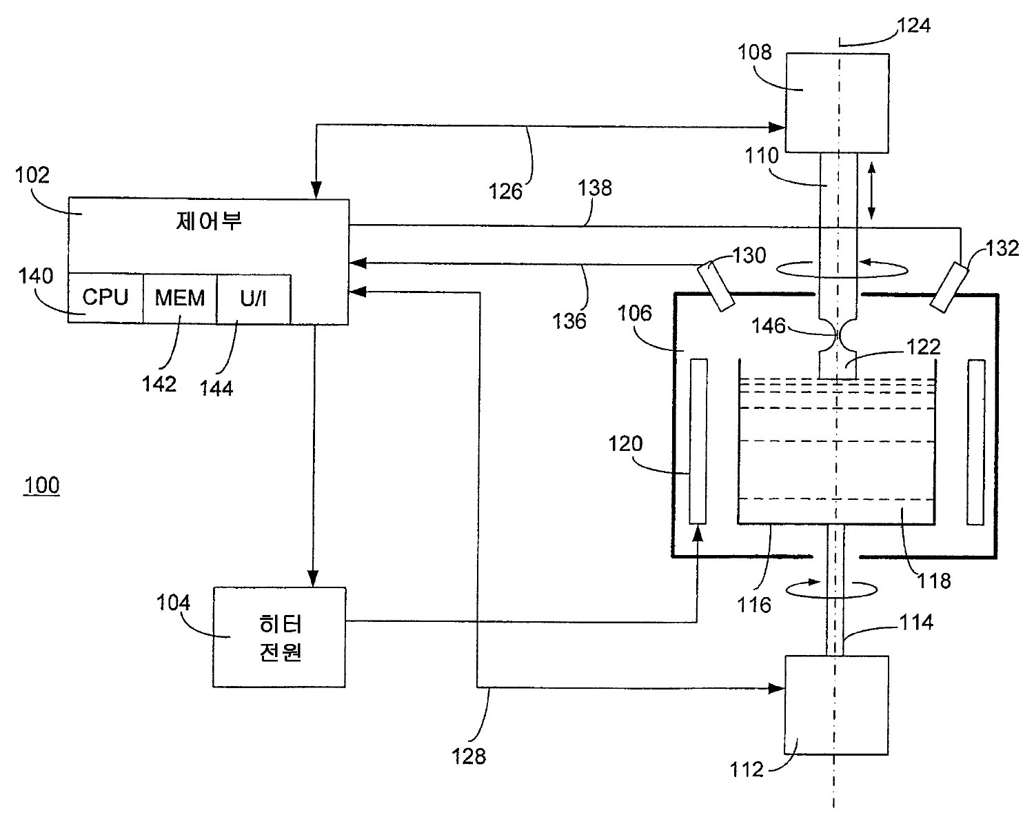
이하, 도면을 참조하면, 도 1 은 예시적인 반도체 결정 성장 장치 (100) 의 블록도이다. 장치 (100) 는 제어부 (102), 히터 전원 (104) 및 결정 성장 챔버 (106) 를 포함한다. 장치 (100) 는 결정 인상부 (108), 결정 샤프트 (110), 도가니 구동부 (112) 및 도가니 구동 샤프트 (114) 를 더 포함한다.Referring now to the drawings, FIG. 1 is a block diagram of an exemplary semiconductor
용융물 (118) 을 포함한 도가니 (116) 및 히터 (120) 는 챔버 (106) 내부에 포함된다. 도 1 의 설명에서, 반도체 결정 (122) 은 용융물 (118) 로부터 형성된다. 제어부 (102) 는 히터 전원 (104) 을 제어하도록 히터 전원 (104) 에 연결된다. 히터 전원 (104) 을 제어함으로써, 용융물 (118) 의 온도는 반도체 결 정 (122) 의 제어된 성장을 허용하도록 제어된다.The
결정 인상부 (108) 는 중심축 (124) 을 따라 결정 샤프트 (110) 를 인상하도록 동작한다. 또한, 결정 인상부 (108) 는 중심축 (124) 에 대해서 결정 샤프트 (110) 를 회전하도록 동작한다. 도 1 에서는, 반시계방향 회전이 도시되나, 시계방향 회전으로 치환될 수도 있고, 결정 인상부 (108) 의 적절한 제어에 의해 양 방향이 이용가능할 수도 있다. 결정 인상 샤프트 (110) 의 회전 또는 이동은 결정 (122) 의 동일한 회전 또는 이동을 야기한다. 결정 인상부 (108) 는 결정 샤프트 (110) 를 인상 및 회전시키기 위한 하나 이상의 전기 모터들 또는 다른 디바이스들을 포함한다. 결정 인상부 (108) 는 제어부 (102) 로부터 제어선 (126) 을 통해 입증된 신호들에 의해 제어된다.The
유사하게, 도가니 구동부 (112) 는 중심축 (124) 을 따라 도가니 구동 샤프트 (114) 를 이동시키고 중심축 (124) 에 대해서 도가니 구동 샤프트 (114) 를 회전하도록 동작한다. 도 1 에서는, 시계방향 회전이 도시되나, 반시계방향 회전으로 치환될 수도 있고, 도가니 구동부 (112) 의 적절한 제어에 의해 양 방향이 이용가능할 수도 있다. 도가니 구동 샤프트 (114) 의 회전 또는 이동은 도가니 (116) 의 동일한 회전 또는 이동을 야기한다. 도가니 구동부 (112) 는 도가니 구동 샤프트 (114) 를 인상 및 회전시키기 위한 하나 이상의 전기 모터들 또는 다른 디바이스들을 포함한다. 도가니 구동부 (112) 는 제어부 (102) 로부터 제어선 (128) 을 통해 입증된 신호들에 의해 제어된다.Similarly, the
결정 (122) 은 도가니 (116) 내의 용융물 (118) 로부터 형성된다. 표면 장력 때문에, 도가니 (116) 내의 고체 및 액체 반도체 재료 사이의 상 계면인 결정화 프론트 (crystallization front) 는 용융물 레벨의 약간 위로 상승된다. 액체 반도체는 결정을 완전히 적시지 않는다. 사실, 이것은 소정각 Θ0 에서 고체 결정과 접촉한다. 이것은 접촉-, 젖음-, 또는 메니스커스-평형각으로서 불린다.Crystal 122 is formed from
용융물 레벨 위로 상승되는 결정 아래의 용융물 영역이 메니스커스라 불린다. 용융물 위로 상승된 결정화 프론트의 위치는 성장 프로세스의 특성들에게 중요하다. 결정화 프론트의 위치가 매우 높이 용융물 위로 상승되는 경우, 결정의 반경은 감소되나; 그렇지 않으면 증가한다.The melt zone below the crystal that rises above the melt level is called meniscus. The location of the crystallization front raised above the melt is important to the characteristics of the growth process. If the position of the crystallization front is raised very high above the melt, the radius of the crystal is reduced; Otherwise increase.
결정 성장 프로세스를 모니터링하는 경우, 챔버 (106) 는 하나 이상의 센서들을 포함한다. 도 1 의 서술된 실시형태에 있어서, 이들 센서들은 카메라 (130) 및 온도 센서 (132) 를 포함한다. 카메라 (130) 는 챔버의 관찰 포트 (viewing port) 근처에 탑재되고, 용융물 (118) 의 표면을 관찰하도록 향하게 된다. 카메라 (130) 는 제어선 (136) 상에 카메라 이미지를 나타내는 신호를 생성하고, 제어부 (102) 로 그 신호를 제공한다. 통상의 기술은 결정 직경의 측정을 제공한다. 이들은 결정 (122) 과 용융물 (118) 사이의 고체-액체 계면에서 형성되는 메니스커스의 도가니 벽의 반사의 특성인 밝은 링 (bright ring) 의 폭을 측정하는 방법을 포함한다. 통상의 밝은 링 및 메니스커스 센서들은 광고온계 (optical pyrometer), 광전지, 광전지를 갖는 회전 거울, 광전지를 갖는 광 원, 라인-스캔 카메라 및 2 차원 어레이 카메라와 같은 디바이스들을 채용한다. 다른 광 측정 디바이스들은 대신하거나 추가하여 이용될 수도 있다. 온도 센서 (132) 는 챔버 (106) 내의 온도를 검출하고, 제어선 (138) 으로 온도를 나타내는 데이터를 제어부 (102) 에 제공한다. 또한, 장치 (100) 는 결정 (122) 의 직경을 측정하도록 구성된 결정 직경 센서를 포함할 수도 있다. 결정 직경 센서는 통상의 임의의 유형일 수도 있다.When monitoring the crystal growth process,
서술된 실시형태의 제어부 (102) 는 일반적으로 중앙 처리부 (CPU) (140), 메모리 (142) 및 사용자 인터페이스 (144) 를 포함한다. CPU (140) 는 마이크로프로세서, 디지털 신호 프로세서, 디지털 로직 기능 또는 컴퓨터와 같은 임의의 적절한 처리 디바이스일 수도 있다. CPU (140) 는 메모리 (142) 내에 저장된 데이터 및 명령들에 따라 동작한다. 게다가, CPU (140) 는 제어선들 (126, 128, 136, 138) 에 의해서와 같이 센서로부터 수신된 데이터 및 다른 정보를 이용하여 동작한다. 여전히 또한, CPU (140) 는 제어 신호들을 발생시켜 히터 전원 (104), 결정 인상부 (108) 및 도가니 구동부 (112) 와 같은 반도체 결정 성장 장치 (100) 의 부분들을 제어하도록 동작한다.The
메모리 (142) 는 반도체 메모리, 자기 또는 광 디스크 또는 이들이나 다른 기억 장치의 임의의 조합과 같은 임의의 유형의 동적 또는 지속성 메모리일 수도 있다. 몇몇 애플리케이션들에서, 본 발명은 CPU (140) 로 하여금 반도체 결정 성장 장치 (100) 의 다른 구성요소들과 함께 소정의 특화된 기능을 수행하게 하는 데이터를 포함한 컴퓨터 판독가능한 저장 매체로서 구체화될 수도 있다.
사용자 인터페이스 (144) 는 반도체 결정 성장 장치 (100) 의 사용자 제어 및 모니터링을 허용한다. 사용자 인터페이스 (144) 는 사용자에게 동작 정보를 제공하기 위한 임의의 적합한 디스플레이를 포함하고, 반도체 결정 성장 장치 (100) 의 사용자 제어 및 구동을 허용하는 임의의 유형의 키보드 또는 스위치들을 포함할 수도 있다.The
반도체 결정 성장 장치 (100) 는 쵸크랄스키 (Czochralski) 프로세스에 따라 단결정 반도체 잉곳의 성장을 가능하게 한다. 본 프로세스에 따라, 실리콘과 같은 반도체 재료는 도가니 (116) 내에 놓인다. 히터 전원 (104) 은 실리콘을 가열하고 그 실리콘을 녹게 하는 히터 (120) 를 구동한다. 히터 (120) 는 실리콘 용융물 (118) 을 액체 상태로 유지시킨다. 통상의 프로세스에 따르면, 시드 결정 (146) 은 결정 인상 샤프트 (110) 에 부착된다. 시드 결정 (146) 은 결정 인상부 (108) 에 의해 용융물 (118) 로 하강된다. 게다가, 결정 인상부 (108) 는 결정 인상 샤프트 (110) 및 시드 결정 (146) 이 반시계방향과 같은 제 1 방향으로 회전하게 하나, 도가니 구동부 (112) 는 도가니 구동 샤프트 (114) 및 도가니 (116) 가 시계방향과 같은 반대 방향으로 회전하게 한다. 도가니 구동부 (112) 는 또한 결정 성장 프로세스 동안 요구되는 것에 따라 도가니 (116) 를 상승 또는 하강시킬 수도 있다. 예를 들어, 결정이 성장됨에 따라 용융물 (118) 이 고갈되므로 용융물 레벨이 실질적으로 일정하게 보상 및 유지하도록 도가니 구동부가 상승된다. 본 프로세스 동안, 히터 전원 (104), 결정 인상부 (108) 및 도가니 구동부 (112) 모두는 제어부 (102) 의 제어 하에서 동작한다.The semiconductor
제어부 (102) 는 결정 (122) 의 성장 동안 반도체 결정 성장 장치 (100) 를 제어하도록 더 동작한다. 이것은 결정 인상부 (108) 의 인상 스피드 및 도가니 구동부 (112) 의 제어 하에서의 도가니 (116) 의 이동의 스피드를 제어하는 것을 포함한다. 본 실시형태들에 따르면, 결정 인상부 (108) 는 평균 인상 스피드에 중첩되는 주기적인 인상 스피드 변화를 더한 평균 인상 스피드에서 결정 (122) 을 인상한다.The
평균 인상 스피드는 자체가 직경 제어 시스템에 의해 발생되는 보정항 Δv 를 더한 목표 인상 스피드 ![]()
![]()
주목되는 바와 같이, 결정이 용융물에서 인상되는 평균 스피드는 의도적으로 다음의 형태로 주기적인 변화와 중첩된다.As noted, the average speed at which crystals are pulled out of the melt intentionally overlaps with periodic changes in the following form.
![]()
![]()
여기서 v0 는 직경 제어 시스템으로부터 나오는 보정항을 더한 목표 인상 스피드로 이루어지는 정상의 인상 스피드이고, ![]()
![]()
![]()
![]()
여기서 ΘS 는 결정 반경이 변화하지 않는 메니스커스 젖음각 Θ0 으로부터의 오프셋 각으로 규정되며 vc 는 결정화 속도이다. 이것은 반경 변화 vr 및 반경 r 의 주기적인 변화를 부과할 것이다.Where Θ S is defined as the offset angle from the meniscus wetting angle Θ 0 where the crystal radius does not change and v c is the crystallization rate. This will impose a periodic change of radius change v r and radius r.

여기서 ![]()
![]()
결정 성장 동안 ![]()
![]()
![]()
![]()
![]()
![]()
평균 성장 속도 vg 가 평균 인상 스피드 v 와 동일해야 하기 때문에, 이후 vg = v 인 경우 Θs 는 식 2.0 에 의해 결정된다. ω 가 너무 크지 않으면, ![]()
![]()
![]()
![]()
![]()
![]()
결정 성장 프론트 (결정-용융물 계면) 에서의 열 전달 평형은 다음과 같이 일차원 근사에 의해 기술된다.The heat transfer equilibrium at the crystal growth front (crystal-melt interface) is described by one-dimensional approximation as follows.
![]()
![]()
여기서 ![]()
![]()
![]()
![]()
GL 에 대한 단순화된 표현은 다음으로 구해질 수 있다.A simplified representation of G L can be found as
![]()
![]()
여기서 h 는 메니스커스 높이이고, ΔTB 는 메니스커스 베이스와 결정 용융물 계면 사이의 온도차이다. GL 에 대한 다른 표현은 특정 결정 성장 조건에 대해서 전개될 수 있다. 식 5.1 로 치환하면, 식 5.0 은 다음과 같이 된다.Where h is the meniscus height and ΔT B is the temperature difference between the meniscus base and the crystal melt interface. Other representations for G L can be developed for specific crystal growth conditions. When substituted with Formula 5.1, Formula 5.0 is as follows.
![]()
![]()
연장된 시간 기간에 대한 성장 속도 vc 의 변화는 h, ΔTB 및 GS 에 대한 영향을 미칠 것이다. 그러나, 인상 스피드 조정 (식 1.0) 에 의해 부과되는 바와 같이 성장 속도 vg 의 작은 주기적인 변화는 주로 h 에 영향을 미치고, ΔTB 및 GS 에 변화가 없을 것이다. 식 6.0 의 미분은 이후 다음과 같이 된다.Changes in growth rate v c over an extended time period will have an effect on h, ΔT B and G S. However, a small periodic change in growth rate v g , as imposed by the pulling speed adjustment (equation 1.0), will mainly affect h and there will be no change in ΔT B and G S. The derivative of Equation 6.0 is then as follows.

식 7.1 은 성장 속도 변화 ![]()
![]()
![]()
![]()
![]()
![]()
![]()
![]()
도 2 는 젖음각 ΘS 및 메니스커스 높이 h 의 변화와 관련한 모델을 나타낸다. 도 2 에서는, 결정 (122) 과 용융물 (118) 사이의 결정화 프론트 (204) 에서 형성된 메니스커스 (202) 가 도시된다. 메니스커스 높이의 작은 변화 ![]()
![]()

![]()
![]()

그리고, 이 경우, GS 는 식 5.0 으로부터 획득될 수 있다. 이로써, 중요한 결정 성장 조건들인 온도 구배들은 결정 직경 변화 및/또는 메니스커스 높이의 인상 스피드 조정-관련된 응답을 측정함으로써 측정될 수 있다. 즉, 시간에 의한 결정 인상 스피드의 조정이 변화하는 경우, 주기적인 신호는 결정 직경의 변화의 형태로 응답을 야기할 것이다. 또한, 이것은 메니스커스 높이의 변화를 야기할 것이다. 결정 직경 및 메니스커스 높이, 이들 값들 양자 모두는 카메라 (도 1) 와 같은 통상의 장비를 이용하여 측정될 수 있다. 이들 변화를 모니터링함으로써, 용융물 및 결정에서 성장 프론트 열 구배들에 대한 특성 (단지 결정 표면에서가 아니라 전체 성장 프론트에 대한 특성) 값들이 산출될 수 있다. 이 정보는 이후 용융물 갭 또는 목표 인상 스피드 등과 같은 고유 결정 특성에 영향을 미치는 관련 프로세스 파라미터들을 제어하도록 이용될 수 있다.And in this case, G S can be obtained from equation 5.0. As such, temperature gradients, which are important crystal growth conditions, can be measured by measuring the change in crystal diameter and / or the pull speed adjustment-related response of the meniscus height. In other words, if the adjustment of the crystal pulling speed with time changes, the periodic signal will cause a response in the form of a change in crystal diameter. This will also cause a change in meniscus height. Crystal diameter and meniscus height, both of these values, can be measured using conventional equipment such as a camera (FIG. 1). By monitoring these changes, the characteristic (characteristics for the growth front thermal gradients in the melt and crystals (characteristics for the entire growth front, not just the crystal surface) can be calculated. This information can then be used to control relevant process parameters that affect the intrinsic crystal properties, such as melt gap or target pull speed.
도 3 은 결정 성장 시스템 (300) 의 일 실시형태를 나타낸다. 시스템 (300) 은 도가니 (306) 으로부터 인상되는 결정 (304) 을 포함한 인상 챔버 (302) 를 포함한다. 용융물 (308) 은 도가니 (306) 내에 담겨 있다. 시스템 (300) 은 열 반사기 콘 (310), 시드 리프트 모터 (312) 및 도가니 리프트 모터 (314) 를 더 포함한다. 시스템 (300) 은 결정 직경 측정 디바이스 (316) 및 연관된 직경 측정 시스템 (322) 을 더 포함한다.3 illustrates one embodiment of a
시스템 (300) 은 제어 시스템을 형성하는 몇몇 요소들을 더 포함한다. 이들 요소들은 목표 인상 스피드 출력 (318), 도가니 용융물 레벨 저하 보상 메커니즘 (320), 직경 제어 메커니즘 (324), 정상의 인상 스피드 v0 을 소정 주파수 ω 및 진폭 ![]()
![]()
제어 시스템은 임의의 적절한 방식으로 형성될 수도 있다. 일 실시형태에서, 제어 시스템은 프로세서 및 메모리를 포함한다. 메모리는 프로세서를 제어하기 위한 데이터와 명령을 저장한다. 프로세서는 데이터 및 명령에 응답하여 목표 인상 스피드 출력 (318), 도가니 용융물 레벨 저하 보상 메커니즘 (320), 직경 제어 메커니즘 (324) 및 디바이스 (326) 와 같은 함수 및 시스템을 구현한다. 또한, 프로세서는 명령 및 데이터를 이용하고, 필터 (328), 필터 함수 (330), 온도 구배 추정 시스템 (332) 및 온도 구배 제어 시스템 (334) 을 구현한다. 본 명세서에서 기술되거나 제안된 임의의 로직 또는 신호 처리 함수는 프로그램된 프로세서, 다른 하드웨어 또는 하드웨어와 소프트웨어 조합 중 어느 하나에 의해 동등하게 수행될 수 있다.The control system may be formed in any suitable manner. In one embodiment, the control system includes a processor and a memory. The memory stores data and instructions for controlling the processor. The processor implements functions and systems such as target
목표 인상 스피드 출력 (318) 은 시드 리프트 모터 (312) 를 위한 공칭 인상 스피드 신호를 제공한다. 이 신호에 응답하여, 모터 (312) 는 결정 (304) 을 리프팅하는 인상 (pull-up) 스피드를 설정하거나 변화시킨다. 공칭 인상 스피드 신호 ![]()
![]()
직경 측정 디바이스 (316) 는 결정 (304) 의 직경을 측정하고 결정 (304) 의 직경을 결정하는 직경 측정 시스템 (322) 에 측정 신호를 제공한다. 직경 측정 시스템 (322) 은 직경 제어 시스템 (324) 에 직경 신호를 제공한다. 직경 제어 시스템 (324) 은 다음으로 결합기 (336) 에 연결되고 결합기 (336) 에 인상 스피드 보정 신호를 제공한다.The
정상의 인상 스피드 v0 을 소정의 주파수 ω 와 진폭 ![]()
![]()
![]()
![]()
![]()
![]()
필터 (328) 는 직경 측정 시스템 (322) 및 직경 제어 시스템 (324) 사이에 배치된다. 직경 측정 시스템 (322) 은 출력 신호 ![]()
![]()
필터 (330) 는 직경 측정 시스템 (322) 과 온도 구배 추정 시스템 (332) 사이에 배치된다. 일 실시형태에서, 필터 (330) 는 직경 신호 ![]()
![]()
![]()
![]()
![]()
![]()
시스템 (300) 은 히터 (340) 및 히터 제어 (342) 를 더 포함한다. 일 실시형태에서, 히터 제어는 시스템 (300) 의 동작을 제어하는 제어부의 일부이다. 히터 (340) 는 히터 제어 (342) 에 응답하여 도가니에 열을 인가하여 소정의 온도에서 용융물을 유지시키도록 동작한다. 히터 제어 (342) 는 직경 제어 시스템 (324) 의 출력에 연결된 입력을 가져 직경 제어 시스템에 의해 생성된 신호를 검출한다. 히터 제어 (342) 는 이로써 직경 제어 시스템 (324) 으로부터의 평균 출력이 0 이도록 히터 (340) 의 전력을 제어하는 피드-백 제어를 형성한다. 바꿔 말해, 평균 인상-스피드는 공칭 인상-스피드와 동일하다.
온도 구배 추정 시스템 (332) 은 값 ω, ![]()
![]()
![]()
![]()
![]()
![]()
결정 (304) 이 용융물 (308) 밖으로 인상됨에 따라, 도가니 (306) 내의 용융물 레벨이 저하된다. 동시에, 도가니 (306) 는 저하하는 도가니 용융물 레벨을 보상하기 위하여 도가니 리프트 모터 (314) 에 의해 상승되고 있다. 보상은 용융물의 위치 및 용융물 표면과 열 반사기 콘 (310) 사이의 갭이 일정하게 유지되도록 행해진다. 이상적으로, 결정 (304) 의 열 구배 GS 는 마찬가지로 일정하게 유지된다.As
결정 (304) 이 용융물 (308) 의 밖으로 인상되는 스피드는 진폭 ![]()
![]()
![]()
![]()
![]()
![]()
직경 신호에 포함되는 작은 직경 조정 정보 ![]()
![]()
![]()
![]()
![]()
![]()
이 모든 것들 동안, 직경 제어 시스템 (324) 은 주파수 ω 차단하는 필터 (328) 를 통해 자신의 입력을 수신하기 때문에 작은 직경 조정에 의한 영향을 받지 않는다.During all of these, the
지금까지는 단지 결정 표면 근처가 아닌 전체 성장 프론트의 특징을 나타내는 인-시츄 성장 프론트 온도 구배 추정을 위한 공지된 방법이 없다. 그러나, 이러한 정보는 결함 분산 등과 같은 고유 결정 특성을 결정하기 때문에 다수의 CZ 생성물을 위해 강력히 요구된다.To date, there are no known methods for estimating in-situ growth front temperature gradients that characterize the entire growth front but only near the crystal surface. However, this information is strongly required for many CZ products because it determines inherent crystal properties such as defect dispersion and the like.
통상의 시스템에 있어서, 고유 결정 특성은 결정이 성장된 후에 분석되고 이러한 정보에 기초하여 온도 구배에 영향을 미치는 파라미터를 처리하는 보정이 행해진다. 복잡하고 그에 수반하여 많은 시간이 소비되는 분석이기 때문에, 이러한 조절은 다음 배치 (batch) 이전에 이용되지 않고 때로는 심지어 그 이후에 이용가능하다.In a typical system, the intrinsic crystal characteristic is analyzed after the crystal is grown and a correction is made to process the parameters that affect the temperature gradient based on this information. Because of the complexity and subsequent time consuming analysis, these adjustments are not used before the next batch and sometimes even later.
특정 프로세스 파라미터의 이러한 배치마다의 조절은 어떤 핫 존 재료에 대한 에이징 효과 (aging effect) 를 보상하기 위해 필요하다. 예를 들어, 그 핫 존의 열 반사 차폐의 열 반사도는 시간에 따라 변한다. 핫-존 설계의 중요한 것은, 열 반사가 결정 및 용융물의 특정 온도 구배를 달성하도록 설계되는 것이다. 자신의 관련 재료 특성이 변함에 따라, 결정 및 용융물의 온도 구배들도 변하며, 이것은 예를 들어, 용융물과 열 반사 차폐 사이의 갭을 조절함으로써 보상될 수 있다.Adjustment of this batch of specific process parameters is necessary to compensate for the aging effect for any hot zone material. For example, the thermal reflectivity of the heat reflecting shield of the hot zone changes over time. The important of the hot-zone design is that the thermal reflection is designed to achieve a specific temperature gradient of the crystal and the melt. As its related material properties change, the temperature gradients of the crystal and melt also change, which can be compensated for, for example, by adjusting the gap between the melt and the heat reflection shielding.
점진적 변화에 더하여, 목표된 구배들로부터의 실제 구배들의 편차를 야기할 수 있는 예상치 못한 인자들이 또한 존재한다. 대부분 이들 인자들은 배치 프로세스에도 불구하고 핫 존이 만들어질 때 허용오차 및 인간 에러와 함께 다뤄져야 한다. 통상의 시스템에서, 이들 인자들은 결정 성장 동안 이미 필요한 정보를 제공할 수 있는 공지된 방법이 존재하지 않기 때문에 전부 보상될 수 없다.In addition to gradual changes, there are also unexpected factors that can cause deviations of the actual gradients from the desired gradients. Most of these factors must be handled with tolerances and human errors when hot zones are created despite the batch process. In a typical system, these factors cannot all be compensated because there is no known way to provide the necessary information already during crystal growth.
현재 개시된 방법 및 장치는 전체 성장 프론트의 특성을 나타내는 용융물 및 결정의 온도 구배의 인-시츄 결정을 대비한다. 이 방법 및 장치의 결과는 요구된 조건으로부터의 편차를 검출하고, 예를 들어, 도가니 리프트 모터 (314) 를 조정하여 용융물 표면과 열 반사 사이의 갭을 변경함으로써 결정 성장 동안 조절을 행하도록 이용될 수 있다.The presently disclosed methods and apparatus contrast in-situ crystals of the temperature gradient of the melt and crystals, which characterize the overall growth front. The results of this method and apparatus can be used to detect deviations from the required conditions and make adjustments during crystal growth, for example by adjusting the
상기로부터, 본 발명은 실질적으로 실시간 결정 성장 프론트 (결정-용융물 계면) 에서 온도 구배값의 계산을 허용한다고 이해될 수 있다. 온도 구배들은 결정 직경 제어, 대량으로 도핑된 결정이 성장되는 동안 결정 형태상의 안정성, 및 벌크 결정 마이크로-결함과 같은 고유 재료 특성에 영향을 미치는 중요한 결정 성장 프로세스 파라미터들이다. 개시된 실시형태들은 온도 구배들 GS 및 GL 에 대한 특성 및 평균값의 인-시츄 관찰 및 계산을 위한 일 방식을 제공한다. 획득 된 값은 전체 성장 프론트의 특성을 나타낸다. 실시형태들은 추가적 하드웨어를 요구하지 않고, 이미 현존하는 제어 및 검출기를 이용한다.From the above, it can be understood that the present invention allows the calculation of the temperature gradient value substantially at the real time crystal growth front (crystal-melt interface). Temperature gradients are important crystal growth process parameters that affect intrinsic material properties such as crystal diameter control, crystal morphology stability during bulk doped crystal growth, and bulk crystal micro-defects. The disclosed embodiments provide one way for in-situ observation and calculation of properties and mean values for temperature gradients G S and G L. The obtained values indicate the characteristics of the entire growth front. Embodiments do not require additional hardware and use existing controls and detectors.
또한, 이들 실시형태들은 문제의 성장 조건을 식별하고 결정 성장 프로그램의 성능을 개선하도록 돕는 것을 용이하게 만든다. 개시된 기술에 기초하여, 제어부 내에서 동작하는 성장 제어 소프트웨어는 적극적으로 원하지 않는 성장 조건들로부터 시스템을 멀리하게 하여 변위 응집 (dislocation nucleation), 형태상의 불안정성, 원하지 않은 마이크로-결함 또는 다른 종류의 주요 수율 손실을 방지한다.In addition, these embodiments make it easy to identify the growth conditions in question and to help improve the performance of the crystal growth program. Based on the disclosed technology, growth control software operating within the controller actively distracts the system from unwanted growth conditions, resulting in dislocation nucleation, morphological instability, unwanted micro-defects or other major yields. Prevent loss.
이로써, 상기 상세한 설명은 한정적이기 보다 설명적으로서 간주되는 것으로서, 또한 본 발명의 사상 및 범위를 정의하도록 의도되는, 모든 균등물을 포함한 다음의 청구범위가 이해되는 것으로서 의도된다.Thus, the foregoing detailed description is intended to be considered as illustrative rather than restrictive, and the following claims are to be understood, including all equivalents, which are intended to define the spirit and scope of the invention.
도 1 은 예시적인 반도체 결정 성장 장치의 블록도.1 is a block diagram of an exemplary semiconductor crystal growth apparatus.
도 2 는 도 1 의 장치에서 제조된 반도체 결정의 젖음각 (wetting angle) 및 메니스커스 높이의 변화를 설명하는 분석적 모델을 나타낸 도면.FIG. 2 shows an analytical model illustrating changes in wetting angle and meniscus height of semiconductor crystals made in the device of FIG. 1. FIG.
도 3 은 반도체 결정을 제조하는 방법을 나타내는 흐름도.3 is a flowchart illustrating a method of manufacturing a semiconductor crystal.
부호의 설명Explanation of the sign
100: 반도체 결정 성장 장치100: semiconductor crystal growth apparatus
102: 제어부102: control unit
104: 히터 전원104: heater power
106: 결정 성장 챔버106: crystal growth chamber
108: 결정 인상부108: Crystal Impression Division
110: 결정 샤프트110: crystal shaft
112: 도가니 구동부112: crucible drive unit
114: 도가니 구동 샤프트114: crucible drive shaft
116: 도가니116: crucible
118: 용융물118: melt
120: 히터120: heater
122: 반도체 결정122: semiconductor crystal
124: 중심축124: central axis
126, 128, 136, 138: 제어선126, 128, 136, 138: control line
130: 카메라130: camera
132: 온도 센서132: temperature sensor
140: 중앙 처리부 (CPU)140: central processing unit (CPU)
142: 메모리142: memory
144: 사용자 인터페이스144: user interface
146: 시드 결정146: seed crystal
202: 메니스커스202: meniscus
204: 결정화 프론트204: crystallization front
300: 결정 성장 시스템300: crystal growth system
302: 인상 챔버302: raising chamber
304: 결정304: crystal
306: 도가니306: crucible
308: 용융물308: melt
310: 열 반사기 콘310: heat reflector cone
312: 시드 리프트 모터312: seed lift motor
314: 도가니 리프트 모터314: crucible lift motor
316: 결정 직경 측정 디바이스316: crystal diameter measurement device
318: 목표 인상 스피드 출력318: target raise speed output
320: 도가니 용융물 레벨 저하 보상 메커니즘320: Crucible melt level reduction compensation mechanism
322: 직경 측정 시스템322: diameter measurement system
324: 직경 제어 시스템324: diameter control system
326: 디바이스326: device
328: 필터328: filter
330: 필터 함수330: filter function
332: 온도 구배 추정 시스템332: temperature gradient estimation system
334: 온도 구배 제어 시스템334: temperature gradient control system
336, 338: 결합기336, 338: combiner
340: 히터340: heater
342: 히터 제어342: heater control
Claims (17)
Applications Claiming Priority (2)
| Application Number | Priority Date | Filing Date | Title |
|---|---|---|---|
| US12/221,229 | 2008-07-31 | ||
| US12/221,229 US8221545B2 (en) | 2008-07-31 | 2008-07-31 | Procedure for in-situ determination of thermal gradients at the crystal growth front |
Publications (2)
| Publication Number | Publication Date |
|---|---|
| KR20100014169A true KR20100014169A (en) | 2010-02-10 |
| KR101424834B1 KR101424834B1 (en) | 2014-08-01 |
Family
ID=41607023
Family Applications (1)
| Application Number | Title | Priority Date | Filing Date |
|---|---|---|---|
| KR1020090070448A KR101424834B1 (en) | 2008-07-31 | 2009-07-31 | Procedure for in-situ determination of thermal gradients at the crystal growth front |
Country Status (5)
| Country | Link |
|---|---|
| US (2) | US8221545B2 (en) |
| JP (1) | JP5657219B2 (en) |
| KR (1) | KR101424834B1 (en) |
| DE (1) | DE102009034076B4 (en) |
| TW (1) | TWI485294B (en) |
Families Citing this family (16)
| Publication number | Priority date | Publication date | Assignee | Title |
|---|---|---|---|---|
| JP4784401B2 (en) * | 2006-05-30 | 2011-10-05 | 株式会社Sumco | Molten liquid level monitoring device in silicon single crystal growth process |
| JP5083001B2 (en) * | 2008-04-08 | 2012-11-28 | 株式会社Sumco | Pulling method of silicon single crystal |
| DE102009056638B4 (en) * | 2009-12-02 | 2013-08-01 | Siltronic Ag | Method for drawing a single crystal of silicon with a section of constant diameter |
| JP5708171B2 (en) * | 2010-04-26 | 2015-04-30 | 株式会社Sumco | Silicon single crystal pulling apparatus and silicon single crystal manufacturing method |
| US8721786B2 (en) | 2010-09-08 | 2014-05-13 | Siemens Medical Solutions Usa, Inc. | Czochralski crystal growth process furnace that maintains constant melt line orientation and method of operation |
| DE102011002599B4 (en) | 2011-01-12 | 2016-06-23 | Solarworld Innovations Gmbh | Process for producing a silicon ingot and silicon ingot |
| CN102445919A (en) * | 2011-12-20 | 2012-05-09 | 北京京仪世纪电子股份有限公司 | Electric control system for gallium arsenide single crystal furnace |
| KR101339149B1 (en) | 2012-01-05 | 2013-12-09 | 주식회사 엘지실트론 | System and method for contrlling ingot growth apparatus |
| CN104514030B (en) * | 2013-09-29 | 2017-01-04 | 内蒙古恒嘉晶体材料有限公司 | Rate of crystalline growth detection method, control method and system |
| WO2016041063A1 (en) * | 2014-09-15 | 2016-03-24 | Materiaux Nieka Inc. | Method and apparatus for preparing an analytical sample by fusion |
| KR102270624B1 (en) | 2014-12-23 | 2021-06-29 | 에스케이이노베이션 주식회사 | Method and apparatus for growth of conical silicon-carbide single-crystal |
| JP6583142B2 (en) * | 2016-05-25 | 2019-10-02 | 株式会社Sumco | Method and apparatus for producing silicon single crystal |
| CN113493926A (en) * | 2020-03-19 | 2021-10-12 | 隆基绿能科技股份有限公司 | Pulling speed control method, device and system |
| CN111910245B (en) * | 2020-07-29 | 2021-10-22 | 华坪隆基硅材料有限公司 | Crystal pulling tail control method and system and computer storage medium |
| US11618971B2 (en) * | 2020-09-29 | 2023-04-04 | Sumco Corporation | Method and apparatus for manufacturing defect-free monocrystalline silicon crystal |
| EP4050131A1 (en) * | 2021-01-11 | 2022-08-31 | Meishan Boya Advanced Materials Co., Ltd. | Crystal growth control method and system |
Family Cites Families (32)
| Publication number | Priority date | Publication date | Assignee | Title |
|---|---|---|---|---|
| US3929557A (en) * | 1973-06-11 | 1975-12-30 | Us Air Force | Periodically and alternately accelerating and decelerating rotation rate of a feed crystal |
| JPS6283395A (en) | 1985-10-08 | 1987-04-16 | Mitsubishi Metal Corp | Diameter control method for single crystal pulling equipment |
| JPH04219388A (en) * | 1990-04-27 | 1992-08-10 | Nkk Corp | Control of diameter of silicon single crystal and apparatus therefor |
| EP0911430B1 (en) * | 1991-04-26 | 2003-04-09 | Mitsubishi Materials Corporation | Single crystal growth method |
| JPH06271388A (en) | 1993-03-22 | 1994-09-27 | Nippon Steel Corp | Method for manufacturing semiconductor single crystal ingot |
| JPH06279177A (en) * | 1993-03-30 | 1994-10-04 | Nippon Steel Corp | Method and apparatus for controlling pulling of single crystal body |
| JPH06316483A (en) * | 1993-04-28 | 1994-11-15 | Komatsu Electron Metals Co Ltd | Production of silicon single crystal |
| US5653799A (en) * | 1995-06-02 | 1997-08-05 | Memc Electronic Materials, Inc. | Method for controlling growth of a silicon crystal |
| US5656078A (en) * | 1995-11-14 | 1997-08-12 | Memc Electronic Materials, Inc. | Non-distorting video camera for use with a system for controlling growth of a silicon crystal |
| JPH09249496A (en) * | 1996-03-12 | 1997-09-22 | Sumitomo Sitix Corp | Method for producing silicon single crystal |
| US5993902A (en) * | 1997-04-09 | 1999-11-30 | Seh America, Inc. | Apparatus and method for extending the lifetime of an exhaust sleeve for growing single crystal silicon by silicon nitride (SI3 N4) coating |
| US5882402A (en) * | 1997-09-30 | 1999-03-16 | Memc Electronic Materials, Inc. | Method for controlling growth of a silicon crystal |
| DE19824838A1 (en) * | 1998-06-04 | 1999-12-09 | Leybold Systems Gmbh | Method of making crystals |
| CN1329682A (en) | 1998-10-14 | 2002-01-02 | Memc电子材料有限公司 | Method and apparatus for accurately pulling crystal |
| US6171391B1 (en) * | 1998-10-14 | 2001-01-09 | Memc Electronic Materials, Inc. | Method and system for controlling growth of a silicon crystal |
| JP4414504B2 (en) | 1999-03-19 | 2010-02-10 | Sumco Techxiv株式会社 | Crystal diameter controller |
| US6776840B1 (en) * | 1999-03-22 | 2004-08-17 | Memc Electronic Materials, Inc. | Method and apparatus for controlling diameter of a silicon crystal in a locked seed lift growth process |
| US6241818B1 (en) * | 1999-04-07 | 2001-06-05 | Memc Electronic Materials, Inc. | Method and system of controlling taper growth in a semiconductor crystal growth process |
| US6203611B1 (en) * | 1999-10-19 | 2001-03-20 | Memc Electronic Materials, Inc. | Method of controlling growth of a semiconductor crystal to automatically transition from taper growth to target diameter growth |
| KR20020081287A (en) * | 2000-02-01 | 2002-10-26 | 엠이엠씨 일렉트로닉 머티리얼즈 인코포레이티드 | Method for controlling growth of a silicon crystal to minimize growth rate and diameter deviations |
| TW546423B (en) * | 2000-05-01 | 2003-08-11 | Komatsu Denshi Kinzoku Kk | Method and apparatus for measuring melt level |
| JP3528758B2 (en) * | 2000-05-31 | 2004-05-24 | 三菱住友シリコン株式会社 | Single crystal pulling device |
| JP4055362B2 (en) * | 2000-12-28 | 2008-03-05 | 信越半導体株式会社 | Single crystal growth method and single crystal growth apparatus |
| JP2004352518A (en) * | 2003-05-27 | 2004-12-16 | Sumitomo Mitsubishi Silicon Corp | Method for manufacturing silicon single crystal |
| JP2005015312A (en) * | 2003-06-27 | 2005-01-20 | Shin Etsu Handotai Co Ltd | Method for manufacturing single crystal, and single crystal |
| JP4457584B2 (en) * | 2003-06-27 | 2010-04-28 | 信越半導体株式会社 | Method for producing single crystal and single crystal |
| US6960254B2 (en) * | 2003-07-21 | 2005-11-01 | Memc Electronic Materials, Inc. | Method to monitor and control the crystal cooling or quenching rate by measuring crystal surface temperature |
| JP2005097049A (en) * | 2003-09-25 | 2005-04-14 | Toshiba Corp | Method for producing silicon single crystal |
| JP5117671B2 (en) * | 2004-10-19 | 2013-01-16 | シルトロン インク | High quality single crystal and growth method thereof |
| US7371283B2 (en) * | 2004-11-23 | 2008-05-13 | Siltron Inc. | Method and apparatus of growing silicon single crystal and silicon wafer fabricated thereby |
| JP4701738B2 (en) * | 2005-02-17 | 2011-06-15 | 株式会社Sumco | Single crystal pulling method |
| US7427325B2 (en) * | 2005-12-30 | 2008-09-23 | Siltron, Inc. | Method for producing high quality silicon single crystal ingot and silicon single crystal wafer made thereby |
-
2008
- 2008-07-31 US US12/221,229 patent/US8221545B2/en active Active
-
2009
- 2009-06-25 TW TW098121377A patent/TWI485294B/en active
- 2009-07-21 DE DE102009034076.9A patent/DE102009034076B4/en active Active
- 2009-07-28 JP JP2009175676A patent/JP5657219B2/en active Active
- 2009-07-31 KR KR1020090070448A patent/KR101424834B1/en active IP Right Grant
-
2012
- 2012-03-29 US US13/434,167 patent/US8673075B2/en active Active
Also Published As
| Publication number | Publication date |
|---|---|
| DE102009034076A1 (en) | 2010-03-25 |
| DE102009034076B4 (en) | 2019-05-09 |
| JP2010037191A (en) | 2010-02-18 |
| TWI485294B (en) | 2015-05-21 |
| US8221545B2 (en) | 2012-07-17 |
| TW201016904A (en) | 2010-05-01 |
| KR101424834B1 (en) | 2014-08-01 |
| JP5657219B2 (en) | 2015-01-21 |
| US20120186512A1 (en) | 2012-07-26 |
| US8673075B2 (en) | 2014-03-18 |
| US20100024718A1 (en) | 2010-02-04 |
Similar Documents
| Publication | Publication Date | Title |
|---|---|---|
| KR101424834B1 (en) | Procedure for in-situ determination of thermal gradients at the crystal growth front | |
| JP5601801B2 (en) | Single crystal silicon ingot growth method and growth apparatus | |
| US5846318A (en) | Method and system for controlling growth of a silicon crystal | |
| KR101028684B1 (en) | Silicon single crystal pulling method | |
| KR101623644B1 (en) | Temperature control module of the ingot growth apparatus and a control method for it | |
| KR20010105416A (en) | Method and system of controlling taper growth in a semiconductor crystal growth process | |
| KR101105588B1 (en) | Method and apparatus for manufacturing high quality silicon single crystal | |
| KR101398304B1 (en) | Reversed action diameter control in a semiconductor crystal growth system | |
| JP3704710B2 (en) | Method of setting seed crystal deposition temperature and silicon single crystal manufacturing apparatus | |
| JP4035924B2 (en) | Single crystal diameter control method and crystal growth apparatus | |
| JP6889170B2 (en) | A method for determining and adjusting the diameter of a single crystal during single crystal pulling | |
| KR101540863B1 (en) | Apparatus for controlling diameter of single crystal ingot and Ingot growing apparatus having the same and method thereof | |
| KR102258435B1 (en) | A method of pulling a single crystal of semiconductor material from a melt contained within a crucible | |
| CN216304033U (en) | System for monitoring state of liquid level of silicon melt in single crystal furnace and state of crucible | |
| JP3484758B2 (en) | Crystal growth apparatus and crystal growth method | |
| KR102662342B1 (en) | Apparatus for controlling ingot growth and method thereof | |
| KR101781463B1 (en) | Apparatus and method for growing silicon single crystal ingot | |
| TWI785410B (en) | Single crystal production system and single crystal production method | |
| JP7583599B2 (en) | Manufacturing method of semiconductor single crystal and manufacturing apparatus of semiconductor single crystal | |
| JP7628952B2 (en) | Method for pulling cylindrical crystals from the melt | |
| JPH0859388A (en) | Single crystal manufacturing equipment |
Legal Events
| Date | Code | Title | Description |
|---|---|---|---|
| PA0109 | Patent application |
Patent event code: PA01091R01D Comment text: Patent Application Patent event date: 20090731 |
|
| PG1501 | Laying open of application | ||
| A201 | Request for examination | ||
| PA0201 | Request for examination |
Patent event code: PA02012R01D Patent event date: 20120720 Comment text: Request for Examination of Application Patent event code: PA02011R01I Patent event date: 20090731 Comment text: Patent Application |
|
| E902 | Notification of reason for refusal | ||
| PE0902 | Notice of grounds for rejection |
Comment text: Notification of reason for refusal Patent event date: 20130905 Patent event code: PE09021S01D |
|
| E701 | Decision to grant or registration of patent right | ||
| PE0701 | Decision of registration |
Patent event code: PE07011S01D Comment text: Decision to Grant Registration Patent event date: 20140520 |
|
| GRNT | Written decision to grant | ||
| PR0701 | Registration of establishment |
Comment text: Registration of Establishment Patent event date: 20140723 Patent event code: PR07011E01D |
|
| PR1002 | Payment of registration fee |
Payment date: 20140723 End annual number: 3 Start annual number: 1 |
|
| PG1601 | Publication of registration | ||
| PR1001 | Payment of annual fee |
Payment date: 20170714 Start annual number: 4 End annual number: 4 |
|
| PR1001 | Payment of annual fee |
Payment date: 20180713 Start annual number: 5 End annual number: 5 |
|
| PR1001 | Payment of annual fee |
Payment date: 20190712 Start annual number: 6 End annual number: 6 |
|
| PR1001 | Payment of annual fee |
Payment date: 20200710 Start annual number: 7 End annual number: 7 |
|
| PR1001 | Payment of annual fee |
Payment date: 20210716 Start annual number: 8 End annual number: 8 |
|
| PR1001 | Payment of annual fee |
Payment date: 20220715 Start annual number: 9 End annual number: 9 |