KR20090086465A - Connection structure of film-form circuit connection material and circuit member - Google Patents
Connection structure of film-form circuit connection material and circuit member Download PDFInfo
- Publication number
- KR20090086465A KR20090086465A KR1020097013931A KR20097013931A KR20090086465A KR 20090086465 A KR20090086465 A KR 20090086465A KR 1020097013931 A KR1020097013931 A KR 1020097013931A KR 20097013931 A KR20097013931 A KR 20097013931A KR 20090086465 A KR20090086465 A KR 20090086465A
- Authority
- KR
- South Korea
- Prior art keywords
- circuit
- film
- connection material
- circuit member
- circuit connection
- Prior art date
- Legal status (The legal status is an assumption and is not a legal conclusion. Google has not performed a legal analysis and makes no representation as to the accuracy of the status listed.)
- Granted
Links
Images


Classifications
-
- C—CHEMISTRY; METALLURGY
- C09—DYES; PAINTS; POLISHES; NATURAL RESINS; ADHESIVES; COMPOSITIONS NOT OTHERWISE PROVIDED FOR; APPLICATIONS OF MATERIALS NOT OTHERWISE PROVIDED FOR
- C09J—ADHESIVES; NON-MECHANICAL ASPECTS OF ADHESIVE PROCESSES IN GENERAL; ADHESIVE PROCESSES NOT PROVIDED FOR ELSEWHERE; USE OF MATERIALS AS ADHESIVES
- C09J4/00—Adhesives based on organic non-macromolecular compounds having at least one polymerisable carbon-to-carbon unsaturated bond ; adhesives, based on monomers of macromolecular compounds of groups C09J183/00 - C09J183/16
-
- C—CHEMISTRY; METALLURGY
- C09—DYES; PAINTS; POLISHES; NATURAL RESINS; ADHESIVES; COMPOSITIONS NOT OTHERWISE PROVIDED FOR; APPLICATIONS OF MATERIALS NOT OTHERWISE PROVIDED FOR
- C09J—ADHESIVES; NON-MECHANICAL ASPECTS OF ADHESIVE PROCESSES IN GENERAL; ADHESIVE PROCESSES NOT PROVIDED FOR ELSEWHERE; USE OF MATERIALS AS ADHESIVES
- C09J5/00—Adhesive processes in general; Adhesive processes not provided for elsewhere, e.g. relating to primers
- C09J5/06—Adhesive processes in general; Adhesive processes not provided for elsewhere, e.g. relating to primers involving heating of the applied adhesive
-
- C—CHEMISTRY; METALLURGY
- C08—ORGANIC MACROMOLECULAR COMPOUNDS; THEIR PREPARATION OR CHEMICAL WORKING-UP; COMPOSITIONS BASED THEREON
- C08G—MACROMOLECULAR COMPOUNDS OBTAINED OTHERWISE THAN BY REACTIONS ONLY INVOLVING UNSATURATED CARBON-TO-CARBON BONDS
- C08G18/00—Polymeric products of isocyanates or isothiocyanates
- C08G18/06—Polymeric products of isocyanates or isothiocyanates with compounds having active hydrogen
- C08G18/08—Processes
- C08G18/10—Prepolymer processes involving reaction of isocyanates or isothiocyanates with compounds having active hydrogen in a first reaction step
-
- C—CHEMISTRY; METALLURGY
- C08—ORGANIC MACROMOLECULAR COMPOUNDS; THEIR PREPARATION OR CHEMICAL WORKING-UP; COMPOSITIONS BASED THEREON
- C08G—MACROMOLECULAR COMPOUNDS OBTAINED OTHERWISE THAN BY REACTIONS ONLY INVOLVING UNSATURATED CARBON-TO-CARBON BONDS
- C08G18/00—Polymeric products of isocyanates or isothiocyanates
- C08G18/06—Polymeric products of isocyanates or isothiocyanates with compounds having active hydrogen
- C08G18/28—Polymeric products of isocyanates or isothiocyanates with compounds having active hydrogen characterised by the compounds used containing active hydrogen
- C08G18/40—High-molecular-weight compounds
- C08G18/42—Polycondensates having carboxylic or carbonic ester groups in the main chain
- C08G18/4205—Polycondensates having carboxylic or carbonic ester groups in the main chain containing cyclic groups
- C08G18/4208—Polycondensates having carboxylic or carbonic ester groups in the main chain containing cyclic groups containing aromatic groups
- C08G18/4211—Polycondensates having carboxylic or carbonic ester groups in the main chain containing cyclic groups containing aromatic groups derived from aromatic dicarboxylic acids and dialcohols
- C08G18/4213—Polycondensates having carboxylic or carbonic ester groups in the main chain containing cyclic groups containing aromatic groups derived from aromatic dicarboxylic acids and dialcohols from terephthalic acid and dialcohols
-
- C—CHEMISTRY; METALLURGY
- C08—ORGANIC MACROMOLECULAR COMPOUNDS; THEIR PREPARATION OR CHEMICAL WORKING-UP; COMPOSITIONS BASED THEREON
- C08G—MACROMOLECULAR COMPOUNDS OBTAINED OTHERWISE THAN BY REACTIONS ONLY INVOLVING UNSATURATED CARBON-TO-CARBON BONDS
- C08G18/00—Polymeric products of isocyanates or isothiocyanates
- C08G18/06—Polymeric products of isocyanates or isothiocyanates with compounds having active hydrogen
- C08G18/28—Polymeric products of isocyanates or isothiocyanates with compounds having active hydrogen characterised by the compounds used containing active hydrogen
- C08G18/40—High-molecular-weight compounds
- C08G18/42—Polycondensates having carboxylic or carbonic ester groups in the main chain
- C08G18/4266—Polycondensates having carboxylic or carbonic ester groups in the main chain prepared from hydroxycarboxylic acids and/or lactones
- C08G18/4269—Lactones
- C08G18/4277—Caprolactone and/or substituted caprolactone
-
- C—CHEMISTRY; METALLURGY
- C08—ORGANIC MACROMOLECULAR COMPOUNDS; THEIR PREPARATION OR CHEMICAL WORKING-UP; COMPOSITIONS BASED THEREON
- C08G—MACROMOLECULAR COMPOUNDS OBTAINED OTHERWISE THAN BY REACTIONS ONLY INVOLVING UNSATURATED CARBON-TO-CARBON BONDS
- C08G18/00—Polymeric products of isocyanates or isothiocyanates
- C08G18/06—Polymeric products of isocyanates or isothiocyanates with compounds having active hydrogen
- C08G18/28—Polymeric products of isocyanates or isothiocyanates with compounds having active hydrogen characterised by the compounds used containing active hydrogen
- C08G18/67—Unsaturated compounds having active hydrogen
- C08G18/671—Unsaturated compounds having only one group containing active hydrogen
- C08G18/672—Esters of acrylic or alkyl acrylic acid having only one group containing active hydrogen
-
- C—CHEMISTRY; METALLURGY
- C08—ORGANIC MACROMOLECULAR COMPOUNDS; THEIR PREPARATION OR CHEMICAL WORKING-UP; COMPOSITIONS BASED THEREON
- C08G—MACROMOLECULAR COMPOUNDS OBTAINED OTHERWISE THAN BY REACTIONS ONLY INVOLVING UNSATURATED CARBON-TO-CARBON BONDS
- C08G18/00—Polymeric products of isocyanates or isothiocyanates
- C08G18/06—Polymeric products of isocyanates or isothiocyanates with compounds having active hydrogen
- C08G18/70—Polymeric products of isocyanates or isothiocyanates with compounds having active hydrogen characterised by the isocyanates or isothiocyanates used
- C08G18/71—Monoisocyanates or monoisothiocyanates
- C08G18/711—Monoisocyanates or monoisothiocyanates containing oxygen in addition to isocyanate oxygen
-
- C—CHEMISTRY; METALLURGY
- C08—ORGANIC MACROMOLECULAR COMPOUNDS; THEIR PREPARATION OR CHEMICAL WORKING-UP; COMPOSITIONS BASED THEREON
- C08G—MACROMOLECULAR COMPOUNDS OBTAINED OTHERWISE THAN BY REACTIONS ONLY INVOLVING UNSATURATED CARBON-TO-CARBON BONDS
- C08G18/00—Polymeric products of isocyanates or isothiocyanates
- C08G18/06—Polymeric products of isocyanates or isothiocyanates with compounds having active hydrogen
- C08G18/70—Polymeric products of isocyanates or isothiocyanates with compounds having active hydrogen characterised by the isocyanates or isothiocyanates used
- C08G18/71—Monoisocyanates or monoisothiocyanates
- C08G18/718—Monoisocyanates or monoisothiocyanates containing silicon
-
- C—CHEMISTRY; METALLURGY
- C08—ORGANIC MACROMOLECULAR COMPOUNDS; THEIR PREPARATION OR CHEMICAL WORKING-UP; COMPOSITIONS BASED THEREON
- C08G—MACROMOLECULAR COMPOUNDS OBTAINED OTHERWISE THAN BY REACTIONS ONLY INVOLVING UNSATURATED CARBON-TO-CARBON BONDS
- C08G18/00—Polymeric products of isocyanates or isothiocyanates
- C08G18/06—Polymeric products of isocyanates or isothiocyanates with compounds having active hydrogen
- C08G18/70—Polymeric products of isocyanates or isothiocyanates with compounds having active hydrogen characterised by the isocyanates or isothiocyanates used
- C08G18/72—Polyisocyanates or polyisothiocyanates
- C08G18/74—Polyisocyanates or polyisothiocyanates cyclic
- C08G18/75—Polyisocyanates or polyisothiocyanates cyclic cycloaliphatic
- C08G18/751—Polyisocyanates or polyisothiocyanates cyclic cycloaliphatic containing only one cycloaliphatic ring
- C08G18/752—Polyisocyanates or polyisothiocyanates cyclic cycloaliphatic containing only one cycloaliphatic ring containing at least one isocyanate or isothiocyanate group linked to the cycloaliphatic ring by means of an aliphatic group
- C08G18/753—Polyisocyanates or polyisothiocyanates cyclic cycloaliphatic containing only one cycloaliphatic ring containing at least one isocyanate or isothiocyanate group linked to the cycloaliphatic ring by means of an aliphatic group containing one isocyanate or isothiocyanate group linked to the cycloaliphatic ring by means of an aliphatic group having a primary carbon atom next to the isocyanate or isothiocyanate group
- C08G18/755—Polyisocyanates or polyisothiocyanates cyclic cycloaliphatic containing only one cycloaliphatic ring containing at least one isocyanate or isothiocyanate group linked to the cycloaliphatic ring by means of an aliphatic group containing one isocyanate or isothiocyanate group linked to the cycloaliphatic ring by means of an aliphatic group having a primary carbon atom next to the isocyanate or isothiocyanate group and at least one isocyanate or isothiocyanate group linked to a secondary carbon atom of the cycloaliphatic ring, e.g. isophorone diisocyanate
-
- C—CHEMISTRY; METALLURGY
- C08—ORGANIC MACROMOLECULAR COMPOUNDS; THEIR PREPARATION OR CHEMICAL WORKING-UP; COMPOSITIONS BASED THEREON
- C08G—MACROMOLECULAR COMPOUNDS OBTAINED OTHERWISE THAN BY REACTIONS ONLY INVOLVING UNSATURATED CARBON-TO-CARBON BONDS
- C08G18/00—Polymeric products of isocyanates or isothiocyanates
- C08G18/06—Polymeric products of isocyanates or isothiocyanates with compounds having active hydrogen
- C08G18/70—Polymeric products of isocyanates or isothiocyanates with compounds having active hydrogen characterised by the isocyanates or isothiocyanates used
- C08G18/72—Polyisocyanates or polyisothiocyanates
- C08G18/74—Polyisocyanates or polyisothiocyanates cyclic
- C08G18/76—Polyisocyanates or polyisothiocyanates cyclic aromatic
- C08G18/7657—Polyisocyanates or polyisothiocyanates cyclic aromatic containing two or more aromatic rings
-
- C—CHEMISTRY; METALLURGY
- C09—DYES; PAINTS; POLISHES; NATURAL RESINS; ADHESIVES; COMPOSITIONS NOT OTHERWISE PROVIDED FOR; APPLICATIONS OF MATERIALS NOT OTHERWISE PROVIDED FOR
- C09J—ADHESIVES; NON-MECHANICAL ASPECTS OF ADHESIVE PROCESSES IN GENERAL; ADHESIVE PROCESSES NOT PROVIDED FOR ELSEWHERE; USE OF MATERIALS AS ADHESIVES
- C09J11/00—Features of adhesives not provided for in group C09J9/00, e.g. additives
- C09J11/02—Non-macromolecular additives
- C09J11/04—Non-macromolecular additives inorganic
-
- C—CHEMISTRY; METALLURGY
- C09—DYES; PAINTS; POLISHES; NATURAL RESINS; ADHESIVES; COMPOSITIONS NOT OTHERWISE PROVIDED FOR; APPLICATIONS OF MATERIALS NOT OTHERWISE PROVIDED FOR
- C09J—ADHESIVES; NON-MECHANICAL ASPECTS OF ADHESIVE PROCESSES IN GENERAL; ADHESIVE PROCESSES NOT PROVIDED FOR ELSEWHERE; USE OF MATERIALS AS ADHESIVES
- C09J175/00—Adhesives based on polyureas or polyurethanes; Adhesives based on derivatives of such polymers
- C09J175/04—Polyurethanes
-
- C—CHEMISTRY; METALLURGY
- C09—DYES; PAINTS; POLISHES; NATURAL RESINS; ADHESIVES; COMPOSITIONS NOT OTHERWISE PROVIDED FOR; APPLICATIONS OF MATERIALS NOT OTHERWISE PROVIDED FOR
- C09J—ADHESIVES; NON-MECHANICAL ASPECTS OF ADHESIVE PROCESSES IN GENERAL; ADHESIVE PROCESSES NOT PROVIDED FOR ELSEWHERE; USE OF MATERIALS AS ADHESIVES
- C09J9/00—Adhesives characterised by their physical nature or the effects produced, e.g. glue sticks
- C09J9/02—Electrically-conducting adhesives
-
- H—ELECTRICITY
- H01—ELECTRIC ELEMENTS
- H01R—ELECTRICALLY-CONDUCTIVE CONNECTIONS; STRUCTURAL ASSOCIATIONS OF A PLURALITY OF MUTUALLY-INSULATED ELECTRICAL CONNECTING ELEMENTS; COUPLING DEVICES; CURRENT COLLECTORS
- H01R12/00—Structural associations of a plurality of mutually-insulated electrical connecting elements, specially adapted for printed circuits, e.g. printed circuit boards [PCB], flat or ribbon cables, or like generally planar structures, e.g. terminal strips, terminal blocks; Coupling devices specially adapted for printed circuits, flat or ribbon cables, or like generally planar structures; Terminals specially adapted for contact with, or insertion into, printed circuits, flat or ribbon cables, or like generally planar structures
- H01R12/50—Fixed connections
- H01R12/51—Fixed connections for rigid printed circuits or like structures
- H01R12/52—Fixed connections for rigid printed circuits or like structures connecting to other rigid printed circuits or like structures
-
- H—ELECTRICITY
- H01—ELECTRIC ELEMENTS
- H01R—ELECTRICALLY-CONDUCTIVE CONNECTIONS; STRUCTURAL ASSOCIATIONS OF A PLURALITY OF MUTUALLY-INSULATED ELECTRICAL CONNECTING ELEMENTS; COUPLING DEVICES; CURRENT COLLECTORS
- H01R4/00—Electrically-conductive connections between two or more conductive members in direct contact, i.e. touching one another; Means for effecting or maintaining such contact; Electrically-conductive connections having two or more spaced connecting locations for conductors and using contact members penetrating insulation
- H01R4/04—Electrically-conductive connections between two or more conductive members in direct contact, i.e. touching one another; Means for effecting or maintaining such contact; Electrically-conductive connections having two or more spaced connecting locations for conductors and using contact members penetrating insulation using electrically conductive adhesives
-
- H—ELECTRICITY
- H05—ELECTRIC TECHNIQUES NOT OTHERWISE PROVIDED FOR
- H05K—PRINTED CIRCUITS; CASINGS OR CONSTRUCTIONAL DETAILS OF ELECTRIC APPARATUS; MANUFACTURE OF ASSEMBLAGES OF ELECTRICAL COMPONENTS
- H05K3/00—Apparatus or processes for manufacturing printed circuits
- H05K3/30—Assembling printed circuits with electric components, e.g. with resistor
- H05K3/32—Assembling printed circuits with electric components, e.g. with resistor electrically connecting electric components or wires to printed circuits
- H05K3/321—Assembling printed circuits with electric components, e.g. with resistor electrically connecting electric components or wires to printed circuits by conductive adhesives
- H05K3/323—Assembling printed circuits with electric components, e.g. with resistor electrically connecting electric components or wires to printed circuits by conductive adhesives by applying an anisotropic conductive adhesive layer over an array of pads
-
- H—ELECTRICITY
- H05—ELECTRIC TECHNIQUES NOT OTHERWISE PROVIDED FOR
- H05K—PRINTED CIRCUITS; CASINGS OR CONSTRUCTIONAL DETAILS OF ELECTRIC APPARATUS; MANUFACTURE OF ASSEMBLAGES OF ELECTRICAL COMPONENTS
- H05K3/00—Apparatus or processes for manufacturing printed circuits
- H05K3/36—Assembling printed circuits with other printed circuits
- H05K3/361—Assembling flexible printed circuits with other printed circuits
-
- H10W72/01325—
-
- H10W72/07251—
-
- H10W72/073—
-
- H10W72/07331—
-
- H10W72/074—
-
- H10W72/20—
-
- H10W72/325—
-
- H10W72/352—
-
- H10W72/354—
-
- H10W72/355—
-
- H10W72/90—
-
- H10W72/923—
-
- H10W72/9415—
Landscapes
- Chemical & Material Sciences (AREA)
- Organic Chemistry (AREA)
- Health & Medical Sciences (AREA)
- Chemical Kinetics & Catalysis (AREA)
- Medicinal Chemistry (AREA)
- Polymers & Plastics (AREA)
- Engineering & Computer Science (AREA)
- Manufacturing & Machinery (AREA)
- Microelectronics & Electronic Packaging (AREA)
- Inorganic Chemistry (AREA)
- Adhesives Or Adhesive Processes (AREA)
- Combinations Of Printed Boards (AREA)
- Adhesive Tapes (AREA)
- Non-Insulated Conductors (AREA)
- Conductive Materials (AREA)
Abstract
본 발명은 제1 회로 기판의 주면 상에 제1 회로 전극이 형성된 제1 회로 부재와, 제2 회로 기판의 주면 상에 제2 회로 전극이 형성된 제2 회로 부재를, 제1 및 제2 회로 전극을 대향시킨 상태에서 전기적으로 접속하기 위한 필름상 회로 접속 재료이며, 필름 형성재와, 라디칼 중합성 화합물과, 가열에 의해 유리 라디칼을 발생하는 라디칼 중합 개시제와, 이소시아네이트기 함유 화합물을 함유하고, 이소시아네이트기 함유 화합물의 함유 비율이 필름 형성재와 라디칼 중합성 화합물의 합계 100 질량부에 대하여 0.09 내지 5 질량부인 필름상 회로 접속 재료에 관한 것이다.The present invention provides a first circuit member in which a first circuit electrode is formed on a main surface of a first circuit board, and a second circuit member in which a second circuit electrode is formed on a main surface of a second circuit board. Is a film-form circuit connection material for electrically connecting in a state of facing each other, and contains a film-forming material, a radically polymerizable compound, a radical polymerization initiator for generating free radicals by heating, and an isocyanate group-containing compound, It is related with the film-form circuit connection material whose content rate of group containing compound is 0.09-5 mass parts with respect to a total of 100 mass parts of a film forming material and a radically polymerizable compound.
Description
본 발명은 필름상 회로 접속 재료 및 회로 부재의 접속 구조에 관한 것이다.This invention relates to the connection structure of a film-form circuit connection material and a circuit member.
최근 들어, 반도체나 액정 디스플레이 등의 분야에서 전자 부품을 고정하거나, 회로 접속을 행하거나 하기 위해서 각종 접착 재료가 사용되고 있다. 이들 용도에서는, 점점 더 고밀도화, 고정밀화가 진행하여, 접착제에도 높은 접착력이나 신뢰성이 요구되고 있다. Background Art In recent years, various adhesive materials have been used to fix electronic components or to make circuit connections in fields such as semiconductors and liquid crystal displays. In these applications, densification and high precision progress more and more, and high adhesive force and reliability are calculated | required also for an adhesive agent.
특히, 액정 디스플레이와 TCP의 접속, FPC와 TCP의 접속, 또는 FPC와 인쇄 배선판의 접속에는 접착제 중에 도전성 입자를 분산시킨 이방 도전성 접착제가 회로 접속 재료로서 사용되고 있다. 또한, 최근에는 반도체 실리콘칩을 기판에 실장하는 경우에도, 종래의 와이어본드 대신에 반도체 실리콘칩을 페이스다운으로 기판에 직접 실장하는, 이른바 플립칩 실장이 행해지고 있고, 여기서도 이방 도전성 접착제의 적용이 개시되어 있다. In particular, an anisotropic conductive adhesive obtained by dispersing conductive particles in an adhesive is used as a circuit connecting material for connecting a liquid crystal display and TCP, connecting an FPC and TCP, or connecting an FPC and a printed wiring board. Moreover, in recent years, even when mounting a semiconductor silicon chip on a board | substrate, what is called flip chip mounting which mounts a semiconductor silicon chip directly to a board face-down instead of the conventional wire bond is performed, and application of an anisotropic conductive adhesive is started here, too. It is.
또한, 최근 들어 정밀 전자 기기의 분야에서는 회로의 고밀도화가 진전되어 전극폭 및 전극 간격이 매우 좁아져 있다. 이 때문에, 종래의 에폭시 수지계를 이용한 회로 접속 재료의 접속 조건에서는 배선의 탈락, 박리, 위치 어긋남이 생기기 쉽게 되어 있다. In recent years, in the field of precision electronic devices, the densification of circuits has advanced, and the electrode width and electrode spacing have become very narrow. For this reason, in connection conditions of the circuit connection material which used the conventional epoxy resin system, the wiring fall | disconnected, peeling, and a position shift tend to occur.
또한, 생산 효율 향상을 위해 접속 시간의 단축화가 요구되고 있고, 10초 이하로 접속할 수 있는 회로 접속 재료가 요구되고 있다. 따라서, 저온 속경화성이 우수하고, 또한 가용 시간이 긴 전기·전자용의 회로 접속 재료가 개발되어 있다(예를 들면, 특허 문헌 1 참조). Further, in order to improve production efficiency, shortening of the connection time is required, and a circuit connection material capable of connecting in 10 seconds or less is required. Therefore, the circuit connection material for electrical and electronics which is excellent in low-temperature fast hardenability and has a long usable time is developed (for example, refer patent document 1).
특허 문헌 1: 일본 특허 공개 (평)11-97825호 공보Patent Document 1: Japanese Patent Application Laid-Open No. 11-97825
[발명의 개시][Initiation of invention]
[발명이 해결하고자 하는 과제][Problem to Solve Invention]
그러나, 상기 회로 접속 재료는 접속하는 회로 부재의 재질에 따라 접착 강도가 다르다. 특히, 회로 부재 표면이 질화규소, 실리콘 수지 또는 폴리이미드 수지로 코팅되어 있거나, 이들 수지가 회로 부재 표면에 부착되어 있거나 하는 경우, 접착 강도가 저하되는 경향이 있다. 따라서, 회로 부재의 재질에 상관없이 접착성이 우수하고, 또한 충분히 긴 가용 시간을 갖는 회로 접속 재료가 요망되고 있다. However, the above-mentioned circuit connection material differs in adhesive strength according to the material of the circuit member to connect. In particular, when the circuit member surface is coated with silicon nitride, a silicone resin or a polyimide resin, or when these resins are attached to the circuit member surface, the adhesive strength tends to be lowered. Therefore, there is a demand for a circuit connection material that is excellent in adhesiveness and has a sufficiently long pot life regardless of the material of the circuit member.
본 발명은 상기 사정을 감안하여 이루어진 것으로서, 회로 부재의 재질에 상관없이 충분히 높은 접착성을 나타내고, 또한 충분히 긴 가용 시간을 갖는 필름상 회로 접속 재료 및 이것을 이용한 회로 부재의 접속 구조를 제공하는 것을 목적으로 한다. The present invention has been made in view of the above circumstances, and an object of the present invention is to provide a film-like circuit connection material having a sufficiently high adhesion and having a sufficiently long pot life regardless of the material of the circuit member and a connection structure of the circuit member using the same. It is done.
[과제를 해결하기 위한 수단][Means for solving the problem]
본 발명은 제1 회로 기판의 주면 상에 제1 회로 전극이 형성된 제1 회로 부재와, 제2 회로 기판의 주면 상에 제2 회로 전극이 형성된 제2 회로 부재를, 제1 및 제2 회로 전극을 대향시킨 상태에서 전기적으로 접속하기 위한 필름상 회로 접속 재료이며, 필름 형성재와, 라디칼 중합성 화합물과, 가열에 의해 유리 라디칼을 발생하는 라디칼 중합 개시제와, 이소시아네이트기 함유 화합물을 함유하고, 이소시아네이트기 함유 화합물의 함유 비율이 필름 형성재와 라디칼 중합성 화합물의 합계 100 질량부에 대하여 0.09 내지 5 질량부인 필름상 회로 접속 재료를 제공한다. The present invention provides a first circuit member in which a first circuit electrode is formed on a main surface of a first circuit board, and a second circuit member in which a second circuit electrode is formed on a main surface of a second circuit board. Is a film-form circuit connection material for electrically connecting in a state of facing each other, and contains a film-forming material, a radically polymerizable compound, a radical polymerization initiator for generating free radicals by heating, and an isocyanate group-containing compound, The film-form circuit connection material whose content rate of group containing compound is 0.09-5 mass parts with respect to a total of 100 mass parts of a film forming material and a radically polymerizable compound.
상기 구성을 구비함으로써 본 발명의 필름상 회로 접속 재료는 회로 부재의 재질에 상관없이 충분히 높은 접착성을 나타내고, 또한 충분히 긴 가용 시간을 갖는 것이 된다. 이러한 효과가 발현할 수 있는 이유는 분명하지 않지만, 본 발명자들은 이하와 같이 추측하고 있다. By providing the said structure, the film-form circuit connection material of this invention exhibits adhesiveness high enough regardless of the material of a circuit member, and has a sufficiently long pot life. The reason why such an effect can be expressed is not clear, but the present inventors speculate as follows.
통상, 회로 접속 재료의 가용 시간을 길게 하기 위해서는 회로 접속 재료의 반응성을 제어할 필요가 있다. 그러나, 회로 접속 재료의 반응성을 제어하여 버리면, 피착체의 종류에 따라서는 충분한 접착성을 나타내기 어려워지는 경향이 있다. 한편, 상기 이소시아네이트기 함유 화합물은 회로 접속 시의 온도 조건 하에서는 반응성이 우수하지만, 그것보다 낮은 온도 하에서는 안정적이라고 생각된다. 따라서, 본 발명의 필름상 회로 접속 재료는 소정량의 이소시아네이트기 함유 화합물을 상술한 다른 성분과 같이 함유함으로써, 양호한 접착성과 충분히 긴 가용 시간을 양립시킬 수 있는 것으로 생각된다. Usually, in order to lengthen the pot life of a circuit connection material, it is necessary to control the reactivity of a circuit connection material. However, when the reactivity of the circuit connection material is controlled, it tends to be difficult to exhibit sufficient adhesiveness depending on the type of adherend. On the other hand, although the said isocyanate group containing compound is excellent in reactivity under the temperature conditions at the time of a circuit connection, it is thought that it is stable under the temperature lower than it. Therefore, it is thought that the film-form circuit connection material of this invention can make favorable adhesiveness and sufficiently long pot life compatible by containing a predetermined amount of isocyanate group containing compound like the other components mentioned above.
상기 필름상 회로 접속 재료는 불소 함유 유기 화합물을 함유하는 것이 바람직하다. 이러한 필름상 회로 접속 재료는 접착성이 더 한층 향상함과 동시에 전사 성도 우수하다는 효과를 발휘한다. It is preferable that the said film-form circuit connection material contains a fluorine-containing organic compound. Such a film-form circuit connection material exhibits the effect that adhesiveness further improves and transferability is also excellent.
또한, 본 발명의 필름상 회로 접속 재료는 필름 형성재로서 중량 평균 분자량 10000 이상의 우레탄 결합을 갖는 유기 화합물을 포함하는 것이 바람직하다. 이에 따라, 필름상 회로 접속 재료의 유연성이 향상하여, 각종 회로 부재와의 접착성이 우수하다는 본 발명의 효과를 한층 유효하게 발휘할 수 있다. Moreover, it is preferable that the film-form circuit connection material of this invention contains the organic compound which has a urethane bond with a weight average molecular weight of 10000 or more as a film formation material. Thereby, the flexibility of a film-form circuit connection material improves and the effect of this invention that it is excellent in adhesiveness with various circuit members can be exhibited more effectively.
본 발명의 회로 접속 재료는 도전성 입자를 추가로 함유하는 것이 바람직하다. 이에 따라, 회로 접속 재료는 그 자체 도전성을 용이하게 가질 수 있다. 그 때문에, 이 회로 접속 재료는 회로 전극이나 반도체 등의 전기 공업이나 전자 공업의 분야에서 도전성 접착제로서 사용할 수 있게 된다. 또한, 이 경우, 회로 접속 재료가 도전성을 갖기 때문에, 경화 후의 접속 저항을 보다 낮게 하는 것이 가능해진다. It is preferable that the circuit connection material of this invention further contains electroconductive particle. Accordingly, the circuit connection material can easily have its own conductivity. Therefore, this circuit connection material can be used as a conductive adhesive in the fields of the electrical industry and the electronics industry, such as a circuit electrode and a semiconductor. In this case, since the circuit connection material has conductivity, it becomes possible to lower the connection resistance after curing.
본 발명은 제1 회로 기판의 주면 상에 제1 회로 전극이 형성된 제1 회로 부재와, 제2 회로 기판의 주면 상에 제2 회로 전극이 형성되고, 제2 회로 전극이 제1 회로 전극과 대향 배치되도록 배치된 제2 회로 부재와, 제1 회로 기판과 제2 회로 기판의 사이에 설치되고, 제1 및 제2 회로 전극이 전기적으로 접속되도록 제1 회로 부재와 제2 회로 부재를 접속하는 회로 접속부를 구비한 회로 부재의 접속 구조이며, 회로 접속부가 전술한 필름상 회로 접속 재료의 경화물에 의해서 형성되어 있는 회로 부재의 접속 구조를 제공한다. According to the present invention, a first circuit member having a first circuit electrode formed on a main surface of a first circuit board, a second circuit electrode formed on a main surface of a second circuit board, and a second circuit electrode facing the first circuit electrode A circuit disposed between the second circuit member and the first circuit board and the second circuit board, the circuit connecting the first circuit member and the second circuit member such that the first and second circuit electrodes are electrically connected. It is a connection structure of the circuit member provided with a connection part, and provides the connection structure of the circuit member in which the circuit connection part is formed of the hardened | cured material of the film-form circuit connection material mentioned above.
이러한 회로 부재의 접속 구조는 회로 접속부가 접착성이 충분히 우수하여, 가용 시간이 충분히 긴 본 발명의 필름상 회로 접속 재료의 경화물에 의해서 형성 되어 있기 때문에, 동일 회로 부재 상에서 인접하는 회로 전극 사이의 절연성을 유지하면서, 대향하는 회로 전극 사이의 저항값을 감소시킬 수 있다. The connection structure of such a circuit member is excellent in adhesiveness, and since the circuit connection part is formed by the hardened | cured material of the film-form circuit connection material of this invention which is long enough the usable time, it is between the adjacent circuit electrodes on the same circuit member. While maintaining the insulation, the resistance value between the opposing circuit electrodes can be reduced.
본 발명의 회로 부재의 접속 구조에 있어서, 제1 및 제2 회로 전극 중 적어도 한쪽은 그 표면이 금, 은, 주석, 백금족의 금속 및 인듐-주석 산화물로 이루어지는 군에서 선택되는 적어도 1종을 포함하는 재료를 포함하는 것이 바람직하다. 이러한 회로 부재의 접속 구조로서는 동일 회로 부재 상에서 인접하는 회로 전극 사이의 절연성을 유지하면서, 대향하는 회로 전극 사이의 저항값을 더 한층 감소시킬 수 있다. In the connection structure of the circuit member of the present invention, at least one of the first and second circuit electrodes includes at least one selected from the group consisting of gold, silver, tin, a platinum group metal and indium-tin oxide. It is preferable to include the material to make. As the connection structure of such a circuit member, the resistance value between opposing circuit electrodes can be further reduced while maintaining the insulation between adjacent circuit electrodes on the same circuit member.
또한, 본 발명의 회로 부재의 접속 구조에 있어서, 제1 및 제2 회로 기판 중 적어도 한쪽은 폴리에틸렌테레프탈레이트, 폴리에테르술폰, 에폭시 수지, 아크릴 수지, 폴리이미드 수지 및 유리로 이루어지는 군에서 선택되는 적어도 1종을 포함하는 재료를 포함하는 기판인 것이 바람직하다. 상기 본 발명의 회로 접속 재료는, 경화하여 회로 접속부를 형성했을 때에 이들 특정한 재료로 구성된 기판과의 사이에서 보다 높은 접착성을 발현할 수 있다. In the connection structure of the circuit member of the present invention, at least one of the first and second circuit boards is at least one selected from the group consisting of polyethylene terephthalate, polyether sulfone, epoxy resin, acrylic resin, polyimide resin, and glass. It is preferable that it is a board | substrate containing the material containing 1 type. The circuit connection material of the said invention can express higher adhesiveness with the board | substrate comprised by these specific materials, when hardening and forming a circuit connection part.
또한, 상기 회로 부재의 접속 구조에 있어서, 제1 및 제2 회로 부재 중 적어도 한쪽과 상술한 회로 접속부 사이에 질화규소, 실리콘 수지, 폴리이미드 수지 및 아크릴 수지로 이루어지는 군에서 선택되는 적어도 1종의 재료를 포함하는 층이 형성되어 있는 것이 바람직하다. 이에 따라, 상기 층이 형성되어 있지 않은 것에 비하여, 회로 부재와 회로 접속부의 접착성이 더 한층 향상된다. In addition, in the connection structure of the said circuit member, at least 1 sort (s) of material chosen from the group which consists of silicon nitride, a silicone resin, a polyimide resin, and an acrylic resin between at least one of a 1st and 2nd circuit member, and a circuit connection part mentioned above. It is preferable that the layer containing is formed. As a result, the adhesion between the circuit member and the circuit connecting portion is further improved as compared with the case where the layer is not formed.
[발명의 효과][Effects of the Invention]
본 발명에 따르면, 회로 부재의 재질에 상관없이 충분히 높은 접착성을 나타내고, 또한 충분히 긴 가용 시간을 갖는 필름상 회로 접속 재료, 및 이들을 이용한 회로 부재의 접속 구조를 제공할 수 있다. According to the present invention, it is possible to provide a film-like circuit connection material that exhibits sufficiently high adhesion and has a sufficiently long pot life regardless of the material of the circuit member, and a connection structure of the circuit member using them.
도 1은 본 발명에 따른 회로 부재의 접속 구조의 일 실시 형태를 도시하는 개략단면도이다. BRIEF DESCRIPTION OF THE DRAWINGS It is a schematic sectional drawing which shows one Embodiment of the connection structure of the circuit member which concerns on this invention.
도 2는 도 1에 도시하는 회로 부재의 접속 구조의 제조 방법의 일례를 개략단면도에 의해 도시하는 공정도이다. FIG. 2 is a process diagram showing, in a schematic cross-sectional view, an example of a method of manufacturing the connection structure of the circuit member shown in FIG. 1.
[부호의 설명][Description of the code]
1: 회로 부재의 회로 접속 구조 1: circuit connection structure of a circuit member
5: 접착제 성분 5: adhesive components
7: 도전성 입자 7: conductive particles
10: 회로 접속부 10: circuit connection
11: 접착제 성분의 경화물 11: Cured product of adhesive component
20: 제1 회로 부재 20: first circuit member
21: 제1 회로 기판 21: first circuit board
21a: 제1 회로 기판 주면 21a: main surface of the first circuit board
22: 제1 회로 전극 22: first circuit electrode
30: 제2 회로 부재 30: second circuit member
31: 제2 회로 기판 31: second circuit board
31a: 제2 회로 기판 주면 31a: main surface of the second circuit board
32: 제2 회로 전극 32: second circuit electrode
40: 필름상 회로 접속 재료40: film-like circuit connection material
[발명을 실시하기 위한 최선의 형태]Best Mode for Carrying Out the Invention
이하, 필요에 따라서 도면을 참조하면서, 본 발명의 바람직한 실시 형태에 대해서 상세히 설명한다. 또한, 도면 중, 동일 요소에는 동일 부호를 붙이는 것으로 하여, 중복하는 설명은 생략한다. 또한, 상하좌우 등의 위치 관계는 특별히 언급이 없는 한 도면에 도시하는 위치 관계에 기초하는 것으로 한다. 또한, 도면의 치수 비율은 도시된 비율에 한정되는 것은 아니다. 또한, 본 명세서에 있어서의 「(메트)아크릴」이란 「아크릴」 및 그것에 대응하는 「메타크릴」을 의미하고, 「(메트)아크릴레이트」란 「아크릴레이트」 및 그것에 대응하는 「메타크릴레이트」를 의미하고, 「(메트)아크릴로일」이란 「아크릴로일」 및 그것에 대응하는 「메타크릴로일」을 의미한다. EMBODIMENT OF THE INVENTION Hereinafter, preferred embodiment of this invention is described in detail, referring drawings as needed. In addition, in drawing, the same code | symbol is attached | subjected to the same element, and the overlapping description is abbreviate | omitted. In addition, unless otherwise indicated, positional relationship, such as up, down, left, and right, shall be based on the positional relationship shown in drawing. In addition, the dimension ratio of drawing is not limited to the ratio shown. In addition, "(meth) acryl" in this specification means "acryl" and "methacryl" corresponding to it, and "(meth) acrylate" means "acrylate" and "methacrylate" corresponding thereto. "(Meth) acryloyl" means "acryloyl" and "methacryloyl" corresponding thereto.
(필름상 회로 접속 재료)(Film circuit connection material)
본 발명의 필름상 회로 접속 재료(회로 접속용 접착 필름)은 제1 회로 기판의 주면 상에 제1 회로 전극이 형성된 제1 회로 부재와, 제2 회로 기판의 주면 상에 제2 회로 전극이 형성된 제2 회로 부재를, 제1 및 제2 회로 전극을 대향시킨 상태에서 전기적으로 접속한다. 본 발명의 필름상 회로 접속 재료는 접착제 성분으로서 필름 형성재와, 라디칼 중합성 화합물과, 가열에 의해 유리 라디칼을 발생하는 라디칼 중합 개시제와, 이소시아네이트기 함유 화합물을 함유하고, 이소시아네이트기 함유 화합물의 함유 비율이 필름 형성재와 라디칼 중합성 화합물의 합계 100 질량부에 대하여 0.09 내지 5 질량부이다. The film circuit connection material (adhesive film for circuit connection) of this invention has the 1st circuit member in which the 1st circuit electrode was formed on the main surface of the 1st circuit board, and the 2nd circuit electrode was formed on the main surface of the 2nd circuit board. The second circuit member is electrically connected in a state where the first and second circuit electrodes are opposed to each other. The film-form circuit connection material of this invention contains a film forming material, a radically polymerizable compound, a radical polymerization initiator which generate | occur | produces a free radical by heating, and an isocyanate group containing compound as an adhesive component, and contains an isocyanate group containing compound. The ratio is 0.09-5 mass parts with respect to a total of 100 mass parts of a film forming material and a radically polymerizable compound.
필름 형성재란 액상물을 고형화하고, 구성 조성물을 필름 형상으로 한 경우에, 그 필름의 취급이 용이하고, 용이하게 찢어지거나, 깨어지거나, 달라붙거나 하지 않는 기계 특성 등을 부여하는 것이고, 통상의 상태에서 필름으로서의 취급이 가능한 것이다. 필름 형성재로서는, 예를 들면 폴리비닐포르말 수지, 폴리스티렌 수지, 폴리비닐부티랄 수지, 폴리에스테르 수지, 폴리에스테르우레탄 수지, 폴리아미드 수지, 폴리우레탄 수지, 폴리아미드이미드 수지, 폴리이미드 수지, 크실렌 수지, 페녹시 수지를 들 수 있다. 또한, 필름 형성재는 라디칼 중합성의 관능기에 의해 변성되어 있을 수도 있다. When the film forming material solidifies a liquid substance and makes a composition composition into a film form, it is easy to handle the film, and gives a mechanical characteristic etc. which are not easily torn, broken, or stuck together, etc., It can be handled as a film in the state of. As a film forming material, For example, polyvinyl formal resin, polystyrene resin, polyvinyl butyral resin, polyester resin, polyesterurethane resin, polyamide resin, polyurethane resin, polyamideimide resin, polyimide resin, xylene Resins and phenoxy resins. In addition, the film forming material may be modified with a radical polymerizable functional group.
본 발명의 필름상 회로 접속 재료는 접착성이 더 한층 우수하다는 관점에서, 필름 형성재로서 우레탄 결합을 갖는 유기 화합물(이하, 「우레탄 화합물」이라 하는 경우가 있음)을 함유하는 것이 바람직하다. 또한, 우레탄 화합물은 우레탄 결합을 그 주쇄 중에 갖는 것이 바람직하고, 우레탄 결합과 동시에 에스테르 결합을 갖는 것이 보다 바람직하다. It is preferable that the film-form circuit connection material of this invention contains the organic compound (henceforth a "urethane compound" hereafter) which has a urethane bond as a film forming material from a viewpoint of further excellent adhesiveness. Moreover, it is preferable that a urethane compound has a urethane bond in the main chain, and it is more preferable to have an ester bond simultaneously with a urethane bond.
이 우레탄 화합물은, 예를 들면 폴리에스테르폴리올과, 디이소시아네이트와의 반응에 의해 얻어진다. 이 반응에 의해 얻어지는 우레탄 화합물은 일반적으로 폴리에스테르우레탄 수지라고 칭해지는 경우가 있다. This urethane compound is obtained by reaction of polyester polyol and diisocyanate, for example. The urethane compound obtained by this reaction may be generally called polyesterurethane resin.
디이소시아네이트로서는, 2,4-톨릴렌디이소시아네이트(TDI), 4,4'-디페닐메탄디이소시아네이트(MDI), 1,6-헥사메틸렌디이소시아네이트(HDI), 이소포론디이소시아네이트(IPDI) 등의, 방향족, 지환족 또는 지방족의 디이소시아네이트가 바람직하게 이용된다. Examples of the diisocyanate include 2,4-tolylene diisocyanate (TDI), 4,4'-diphenylmethane diisocyanate (MDI), 1,6-hexamethylene diisocyanate (HDI) and isophorone diisocyanate (IPDI). , Aromatic, cycloaliphatic or aliphatic diisocyanates are preferably used.
폴리에스테르폴리올은, 예를 들면 디카르복실산과 디올의 반응에 의해 얻어진다. 디카르복실산으로서는 테레프탈산, 이소프탈산, 아디프산, 세박산 등의 방향족이나 지방족 디카르복실산이 바람직하다. 디올로서는 에틸렌글리콜, 프로필렌글리콜, 1,4-부탄디올, 헥산디올, 네오펜틸글리콜, 디에틸렌글리콜, 트리에틸렌글리콜과 같은 글리콜류가 바람직하다. Polyester polyol is obtained by reaction of dicarboxylic acid and diol, for example. As dicarboxylic acid, aromatic and aliphatic dicarboxylic acids, such as terephthalic acid, isophthalic acid, adipic acid, and sebacic acid, are preferable. As the diol, glycols such as ethylene glycol, propylene glycol, 1,4-butanediol, hexanediol, neopentyl glycol, diethylene glycol and triethylene glycol are preferable.
우레탄 화합물은 중량 평균 분자량이 10000 이상인 것이 바람직하다. 우레탄 화합물의 중량 평균 분자량이 10000 미만이면 필름 형성성이 저하되는 경향이 있다. 또한, 우레탄 화합물의 중량 평균 분자량의 상한값은, 특별히 한정되지 않지만, 중량 평균 분자량이 너무 크면, 용제에의 용해성이나 상용성이 저하되어, 필름상으로 성형하기 위한 도공액을 제조하는 것이 곤란해지는 경향이 있기 때문에 200000 정도가 바람직하다. It is preferable that a urethane compound has a weight average molecular weight of 10000 or more. When the weight average molecular weight of a urethane compound is less than 10000, there exists a tendency for film formability to fall. In addition, although the upper limit of the weight average molecular weight of a urethane compound is not specifically limited, When the weight average molecular weight is too large, the solubility and compatibility to a solvent fall, and it becomes difficult to manufacture the coating liquid for shape | molding in a film form. Since this is about 200,000 is preferable.
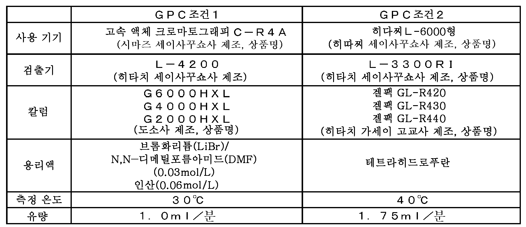
본 명세서에 있어서의 중량 평균 분자량은 표 1에 나타내는 조건에 따라서 겔 투과 크로마토그래피(GPC) 분석에 의해 측정하고, 표준 폴리스티렌의 검량선을 사용하여 환산함으로써 구해진다. 또한, GPC 조건 1은 폴리이미드 수지의 중량 평균 분자량을 측정할 때의 조건이고, GPC 조건 2는 폴리이미드 수지 이외의 유기 화합물의 중량 평균 분자량을 측정할 때의 조건이다. The weight average molecular weight in this specification is measured by gel permeation chromatography (GPC) analysis according to the conditions shown in Table 1, and is calculated | required by converting using the analytical curve of a standard polystyrene. In addition,
라디칼 중합성 화합물이란 라디칼 중합 가능한 관능기를 갖는 것이다. 라디칼 중합성 화합물로서는, 예를 들면 (메트)아크릴산 화합물, 말레이미드 화합물 또는 스티렌 유도체가 바람직하게 이용된다. 이들 라디칼 중합성 화합물은 중합성 단량체 및 중합성 올리고머 중의 어느 것일 수도 있고, 중합성 단량체와 중합성 올리고머를 병용하는 것도 가능하다. 중합성 올리고머는 일반적으로 고점도이기 때문에, 중합성 올리고머를 이용하는 경우, 저점도의 중합성 다관능 (메트)아크릴레이트 등의 중합성 단량체를 병용하여 점도 조정하는 것이 바람직하다. A radically polymerizable compound is a thing which has a functional group which can be radically polymerized. As a radically polymerizable compound, a (meth) acrylic acid compound, a maleimide compound, or a styrene derivative is used preferably, for example. These radically polymerizable compounds may be any of a polymerizable monomer and a polymerizable oligomer, and it is also possible to use a polymerizable monomer and a polymerizable oligomer together. Since a polymerizable oligomer is generally high viscosity, when using a polymerizable oligomer, it is preferable to adjust viscosity by using together polymerizable monomers, such as a low viscosity polymerizable polyfunctional (meth) acrylate.
(메트)아크릴산 화합물로서는, 예를 들면 에폭시(메트)아크릴레이트올리고머, 우레탄(메트)아크릴레이트올리고머, 폴리에테르(메트)아크릴레이트올리고머 및 폴리에스테르(메트)아크릴레이트올리고머 등의 광 중합성 올리고머, 트리메틸올프로판트리(메트)아크릴레이트, 폴리에틸렌글리콜디(메트)아크릴레이트, 폴리알킬렌글리콜디(메트)아크릴레이트, 디시클로펜테닐(메트)아크릴레이트, 디시클로펜테닐옥시에틸(메트)아크릴레이트, 네오펜틸글리콜디(메트)아크릴레이트, 디펜타에리트리톨헥사(메트)아크릴레이트, 이소시아누르산 변성 2관능 (메트)아크릴레이트, 이소시아누르산 변성 3관능 (메트)아크릴레이트, 2,2'-디(메트)아크릴로일옥시디에틸포스페이트 및 2-(메트)아크릴로일옥시에틸액시드포스페이트 등의 다관능 (메트)아크릴레이트 화합물, 펜타에리트리톨(메트)아크릴레이트, 2-시아노에틸(메트)아크릴레이트, 시클로헥실(메트)아크릴레이트, 2-(2-에톡시에톡시)에틸(메트)아크릴레이트, 2-에톡시에틸(메트)아크릴레이트, 2-에틸헥실(메트)아크릴레이트, n-헥실(메트)아크릴레이트, 2-히드록시에틸(메트)아크릴레이트, 히드록시프로필(메트)아크릴레이트, 이소보르닐(메트)아크릴레이트, 이소데실(메트)아크릴레이트, 이소옥틸(메트)아크릴레이트, n-라우릴(메트)아크릴레이트, 2-메톡시에틸(메트)아크릴레이트, 2-페녹시에틸(메트)아크릴레이트, 테트라히드로푸르푸릴(메트)아크릴레이트, 네오펜틸글리콜디(메트)아크릴레이트, t-부틸아미노에틸(메트)아크릴레이트, 시클로헥실(메트)아크릴레이트, 디시클로펜테닐옥시에틸(메트)아크릴레이트, 2-히드록시에틸(메트)아크릴레이트, 이소보르닐(메트)아크릴레이트, 이소데실(메트)아크릴레이트, n-라우릴(메트)아크릴레이트, 스테아릴(메트)아크릴레이트, 트리데실(메트)아크릴레이트 및 글리시딜(메트)아크릴레이트를 들 수 있다. As a (meth) acrylic acid compound, For example, photopolymerizable oligomers, such as an epoxy (meth) acrylate oligomer, a urethane (meth) acrylate oligomer, a polyether (meth) acrylate oligomer, and a polyester (meth) acrylate oligomer, Trimethylolpropane tri (meth) acrylate, polyethylene glycol di (meth) acrylate, polyalkylene glycol di (meth) acrylate, dicyclopentenyl (meth) acrylate, dicyclopentenyloxyethyl (meth) acrylic Latex, neopentyl glycol di (meth) acrylate, dipentaerythritol hexa (meth) acrylate, isocyanuric acid modified bifunctional (meth) acrylate, isocyanuric acid modified trifunctional (meth) acrylate, 2 Multifunctional (meth) acrylate compound such as 2'-di (meth) acryloyloxydiethyl phosphate and 2- (meth) acryloyloxyethyl acid phosphate , Pentaerythritol (meth) acrylate, 2-cyanoethyl (meth) acrylate, cyclohexyl (meth) acrylate, 2- (2-ethoxyethoxy) ethyl (meth) acrylate, 2-ethoxy Ethyl (meth) acrylate, 2-ethylhexyl (meth) acrylate, n-hexyl (meth) acrylate, 2-hydroxyethyl (meth) acrylate, hydroxypropyl (meth) acrylate, isobornyl ( Meth) acrylate, isodecyl (meth) acrylate, isooctyl (meth) acrylate, n-lauryl (meth) acrylate, 2-methoxyethyl (meth) acrylate, 2-phenoxyethyl (meth) Acrylate, tetrahydrofurfuryl (meth) acrylate, neopentylglycoldi (meth) acrylate, t-butylaminoethyl (meth) acrylate, cyclohexyl (meth) acrylate, dicyclopentenyloxyethyl (meth ) Acrylate, 2-hydroxyethyl (meth) acrylate, isobornyl ( Meth) acrylate, isodecyl (meth) acrylate, n-lauryl (meth) acrylate, stearyl (meth) acrylate, tridecyl (meth) acrylate and glycidyl (meth) acrylate. have.
(메트)아크릴산 화합물은 1종을 단독으로 또는 2종 이상을 조합하여 이용된다. 회로 접속 재료의 경화 수축을 억제하고 유연성을 제공하기 위해서는 우레탄(메트)아크릴레이트올리고머를 배합하는 것이 바람직하다. A (meth) acrylic acid compound is used individually by 1 type or in combination of 2 or more types. In order to suppress the cure shrinkage of a circuit connection material and to provide flexibility, it is preferable to mix | blend a urethane (meth) acrylate oligomer.
말레이미드 화합물로서는 분자 중에 말레이미드기를 2개 이상 함유하는 것이 바람직하다. 그 구체예로서는, 1-메틸-2,4-비스말레이미드벤젠, N,N'-m-페닐렌비스말레이미드, N,N'-p-페닐렌비스말레이미드, N,N'-m-톨루일렌비스말레이미드, N,N'-4,4-비페닐렌비스말레이미드, N,N'-4,4-(3,3'-디메틸-비페닐렌)비스말레이미드, N,N'-4,4-(3,3'-디메틸디페닐메탄)비스말레이미드, N,N'-4,4-(3,3'-디에틸디페닐메탄)비스말레이미드, N,N'-4,4-디페닐메탄비스말레이미드, N,N'-4,4-디페닐프로판비스말레이미드, N,N'-4,4-디페닐에테르비스말레이미드, N,N'-3,3'-디페닐술폰비스말레이미드, 2,2-비스[4-(4-말레이미드페녹시)페닐]프로판, 2,2-비스[3-s-부틸-4-(4-말레이미드페녹시)페닐]프로판, 1,1-비스[4-(4-말레이미드페녹시)페닐]데칸, 4,4'-시클로헥실리덴-비스[1-(4-말레이미드페녹시)-2-시클로헥실벤젠] 및 2,2-비스[4-(4-말레이미드페녹시)페닐]헥사플루오로프로판을 들 수 있다. As a maleimide compound, what contains two or more maleimide groups in a molecule | numerator is preferable. Specific examples thereof include 1-methyl-2,4-bismaleimidebenzene, N, N'-m-phenylenebismaleimide, N, N'-p-phenylenebismaleimide, N, N'-m- Toluylene bismaleimide, N, N'-4,4-biphenylenebismaleimide, N, N'-4,4- (3,3'-dimethyl-biphenylene) bismaleimide, N, N '-4,4- (3,3'-dimethyldiphenylmethane) bismaleimide, N, N'-4,4- (3,3'-diethyldiphenylmethane) bismaleimide, N, N' -4,4-diphenylmethanebismaleimide, N, N'-4,4-diphenylpropanebismaleimide, N, N'-4,4-diphenyletherbismaleimide, N, N'-3 , 3'-diphenylsulfonbismaleimide, 2,2-bis [4- (4-maleimidephenoxy) phenyl] propane, 2,2-bis [3-s-butyl-4- (4-maleimide Phenoxy) phenyl] propane, 1,1-bis [4- (4-maleimidephenoxy) phenyl] decane, 4,4'-cyclohexylidene-bis [1- (4-maleimidephenoxy)- 2-cyclohexylbenzene] and 2,2-bis [4- (4-maleimidephenoxy) phenyl] hexafluoropropane.
말레이미드 화합물은 1종을 단독으로 또는 2종 이상을 조합하여 이용된다. A maleimide compound is used individually by 1 type or in combination of 2 or more types.
본 발명의 필름상 회로 접속 재료는 접착성을 향상시키는 목적으로, 라디칼 중합성 화합물로서, 인산에스테르형(메트)아크릴레이트를 함유하는 것이 바람직하다. 인산에스테르형(메트)아크릴레이트를 함유함으로써 필름상 회로 접속 재료는 특히 금속 등의 무기 재료와의 접착성이 향상된다. 인산에스테르형(메트)아크릴레이트로서는 특별히 제한없이 공지된 것을 사용할 수 있다. 그 구체예로서는 하기 화학식 (2)로 표시되는 화합물을 들 수 있다. It is preferable that the film-form circuit connection material of this invention contains a phosphate ester type (meth) acrylate as a radically polymerizable compound for the purpose of improving adhesiveness. By containing a phosphate ester type (meth) acrylate, especially a film-form circuit connection material improves adhesiveness with inorganic materials, such as a metal. As phosphate ester type (meth) acrylate, a well-known thing can be used without a restriction | limiting in particular. As the specific example, the compound represented by following General formula (2) is mentioned.

여기서, n은 1 내지 3의 정수를 나타낸다. Here, n represents the integer of 1-3.
일반적으로, 인산에스테르형(메트)아크릴레이트는 무수인산과 2-히드록시에틸(메트)아크릴레이트의 반응물로서 얻어진다. 인산에스테르형(메트)아크릴레이트로서, 구체적으로는 모노(2-메타크릴로일옥시에틸)액시드포스페이트, 디(2-메타크릴로일옥시에틸)액시드포스페이트를 들 수 있다. 이들은 1종을 단독으로 또는 2종 이상을 조합하여 이용된다. Generally, phosphate ester type (meth) acrylate is obtained as a reactant of phosphoric anhydride and 2-hydroxyethyl (meth) acrylate. Specific examples of the phosphate ester (meth) acrylate include mono (2-methacryloyloxyethyl) acid phosphate and di (2-methacryloyloxyethyl) acid phosphate. These are used individually by 1 type or in combination of 2 or more types.
본 발명의 필름상 회로 접속 재료는 접착성이 더 우수하다는 관점에서 알릴(메트)아크릴레이트를 포함할 수 있다. 알릴(메트)아크릴레이트의 배합 비율은 필름 형성재와 라디칼 중합성 화합물의 합계 100 질량부에 대하여 0.1 내지 10 질량부인 것이 바람직하고, 0.5 내지 5 질량부인 것이 보다 바람직하다. The film-form circuit connection material of this invention can contain an allyl (meth) acrylate from a viewpoint of the adhesiveness being more excellent. It is preferable that it is 0.1-10 mass parts with respect to a total of 100 mass parts of a film forming material and a radically polymerizable compound, and, as for the compounding ratio of allyl (meth) acrylate, it is more preferable that it is 0.5-5 mass parts.
또한, 가열에 의해 유리 라디칼을 발생하는 라디칼 중합 개시제로서는 종래 알려져 있는 과산화 화합물(유기 과산화물) 및 아조 화합물이 이용된다. As the radical polymerization initiator that generates free radicals by heating, conventionally known peroxide compounds (organic peroxides) and azo compounds are used.
유기 과산화물 및 아조 화합물은 주로 가열에 의해 유리 라디칼을 발생한다. 이들 화합물을 라디칼 중합 개시제로서 이용하는 경우, 유기 과산화물 및/또는 아조 화합물로부터 1종 또는 2종 이상을 목적으로 하는 접속 온도, 접속 시간, 가용 시간(이하, 「포트라이프」이라 하는 경우가 있음) 등에 의해 적절하게 선택한다. Organic peroxides and azo compounds generate free radicals primarily by heating. When using these compounds as a radical polymerization initiator, the connection temperature, connection time, availability time (henceforth "port life") etc. which aim at 1 type, or 2 or more types from organic peroxide and / or azo compound, etc. By appropriate selection.
유기 과산화물로서는, 높은 반응성과 긴 포트라이프를 양립시킨다는 관점에서 10시간 반감기 온도가 40℃ 이상, 또한 1분간 반감기 온도가 180℃ 이하인 유기 과산화물이 바람직하고, 10시간 반감기 온도가 60℃ 이상, 또한 1분간 반감기 온도가 170℃ 이하인 유기 과산화물이 보다 바람직하다. 또한, 유기 과산화물은 회로 부재의 회로 전극(접속 단자)의 부식을 방지하기 위해서, 염소 이온이나 유기산의 함유량이 5000 질량 ppm 이하인 것이 바람직하다. 또한, 유기 과산화물은 가열 분해후에 발생하는 유기산이 적은 것이 보다 바람직하다. As the organic peroxide, an organic peroxide having a half-life temperature of 40 ° C. or higher and a half-life temperature of 180 ° C. or lower for 10 minutes is preferable from the viewpoint of achieving both high reactivity and a long pot life, and a 10-hour half-life temperature of 60 ° C. or higher. More preferred is an organic peroxide having a half-life temperature of 170 ° C. or less. In addition, in order to prevent corrosion of the circuit electrode (connection terminal) of a circuit member, organic peroxide is preferable that content of chlorine ion and an organic acid is 5000 mass ppm or less. In addition, the organic peroxide is more preferably less organic acid generated after thermal decomposition.
유기 과산화물로서는, 구체적으로는 디아실퍼옥사이드, 퍼옥시디카르보네이트, 퍼옥시에스테르, 퍼옥시케탈, 디알킬퍼옥사이드, 하이드로퍼옥사이드 및 실릴퍼옥사이드로 이루어지는 군에서 선택되는 1종 이상의 유기 과산화물이 바람직하다. 이 중에서는, 보존 시의 높은 보존 안정성과 사용 시의 높은 반응성을 양립시킨다는 관점에서, 퍼옥시에스테르, 퍼옥시케탈, 디알킬퍼옥사이드, 하이드로퍼옥사이드 및 실릴퍼옥사이드로 이루어지는 군에서 선택되는 1종 이상의 유기 과산화물이 보다 바람직하다. 나아가서는, 보다 높은 반응성이 얻어진다는 점에서 유기 과산화물이 퍼옥시에스테르 및/또는 퍼옥시케탈인 것이 더욱 바람직하다. As the organic peroxide, at least one organic peroxide selected from the group consisting of diacyl peroxide, peroxydicarbonate, peroxy ester, peroxy ketal, dialkyl peroxide, hydroperoxide and silyl peroxide is particularly preferable. Do. Among them, one type selected from the group consisting of peroxy ester, peroxy ketal, dialkyl peroxide, hydroperoxide and silyl peroxide from the viewpoint of achieving both high storage stability at the time of storage and high reactivity at the time of use. The above organic peroxide is more preferable. Furthermore, it is more preferable that the organic peroxide is peroxyester and / or peroxyketal in that higher reactivity is obtained.
디아실퍼옥사이드로서는, 예를 들면 이소부틸퍼옥사이드, 2,4-디클로로벤조일퍼옥사이드, 3,5,5-트리메틸헥사노일퍼옥사이드, 옥타노일퍼옥사이드, 라우로일퍼옥사이드, 스테아로일퍼옥사이드, 숙신산퍼옥사이드, 벤조일퍼옥시톨루엔 및 벤조일퍼옥사이드를 들 수 있다. 이들은 1종을 단독으로 또는 2종 이상을 조합하여 이용된다. Examples of the diacyl peroxide include isobutyl peroxide, 2,4-dichlorobenzoyl peroxide, 3,5,5-trimethylhexanoyl peroxide, octanoyl peroxide, lauroyl peroxide, stearoyl peroxide, and succinic acid. Peroxide, benzoyl peroxy toluene, and benzoyl peroxide are mentioned. These are used individually by 1 type or in combination of 2 or more types.
디알킬퍼옥사이드로서는, 예를 들면 α,α'-비스(t-부틸퍼옥시)디이소프로필벤젠, 디쿠밀퍼옥사이드, 2,5-디메틸-2,5-디(t-부틸퍼옥시)헥산 및 t-부틸쿠밀퍼옥사이드를 들 수 있다. 이들은 1종을 단독으로 또는 2종 이상을 조합하여 이용된다. As the dialkyl peroxide, for example, α, α'-bis (t-butylperoxy) diisopropylbenzene, dicumylperoxide, 2,5-dimethyl-2,5-di (t-butylperoxy) hexane And t-butyl cumyl peroxide. These are used individually by 1 type or in combination of 2 or more types.
퍼옥시디카르보네이트로서는, 예를 들면 디-n-프로필퍼옥시디카르보네이트, 디이소프로필퍼옥시디카르보네이트, 비스(4-t-부틸시클로헥실)퍼옥시디카르보네이트, 디-2-에톡시메톡시퍼옥시디카르보네이트, 비스(2-에틸헥실퍼옥시)디카르보네이트, 디메톡시부틸퍼옥시디카르보네이트 및 비스(3-메틸-3-메톡시부틸퍼옥시)디카르보네이트를 들 수 있다. 이들은 1종을 단독으로 또는 2종 이상을 조합하여 이용된다.As peroxy dicarbonate, di-n-propyl peroxy dicarbonate, diisopropyl peroxy dicarbonate, bis (4-t- butylcyclohexyl) peroxy dicarbonate, di-2-, for example Ethoxymethoxy peroxydicarbonate, bis (2-ethylhexylperoxy) dicarbonate, dimethoxybutylperoxydicarbonate and bis (3-methyl-3-methoxybutylperoxy) dicarbonate Can be. These are used individually by 1 type or in combination of 2 or more types.
퍼옥시에스테르로서는, 예를 들면 쿠밀퍼옥시네오데카노에이트, 1,1,3,3-테트라메틸부틸퍼옥시네오데카노에이트, 1-시클로헥실-1-메틸에틸퍼옥시네오데카노에이트, t-헥실퍼옥시네오데카노에이트, t-부틸퍼옥시피발레이트, 1,1,3,3-테트라메틸부틸퍼옥시-2-에틸헥사노에이트, 2,5-디메틸-2,5-비스(2-에틸헥사노일퍼옥시)헥산, 1-시클로헥실-1-메틸에틸퍼옥시-2-에틸헥사노에이트, t-헥실퍼옥시-2-에틸헥사노에이트, t-부틸퍼옥시-2-에틸헥사노에이트, t-부틸퍼옥시이소부티레이트, 1,1-비스(t-부틸퍼옥시)시클로헥산, t-헥실퍼옥시이소프로필모노카르보네이트, t-부틸퍼옥시-3,5,5-트리메틸헥사노에이트, t-부틸퍼옥시라우레이트, 2,5-디메틸-2,5-비스(m-톨루오일퍼옥시)헥산, t-부틸퍼옥시이소프로필모노카르보네이트, t-부틸퍼옥시-2-에틸헥실모노카르보네이트, t-헥실퍼옥시벤조에이트, t-부틸퍼옥시아세테이트 및 비스(t-부틸퍼옥시)헥사히드로테레프탈레이트를 들 수 있다. 이들은 1종을 단독으로 또는 2종 이상을 조합하여 이용된다. As peroxy ester, for example, cumyl peroxy neodecanoate, 1,1,3,3- tetramethylbutyl peroxy neodecanoate, 1-cyclohexyl-1-methylethyl peroxy neodecanoate, t-hexyl peroxy neodecanoate, t-butyl peroxy pivalate, 1,1,3,3-tetramethylbutylperoxy-2-ethylhexanoate, 2,5-dimethyl-2,5-bis (2-ethylhexanoylperoxy) hexane, 1-cyclohexyl-1-methylethylperoxy-2-ethylhexanoate, t-hexylperoxy-2-ethylhexanoate, t-butylperoxy-2 Ethylhexanoate, t-butylperoxyisobutyrate, 1,1-bis (t-butylperoxy) cyclohexane, t-hexylperoxyisopropyl monocarbonate, t-butylperoxy-3,5 , 5-trimethylhexanoate, t-butylperoxylaurate, 2,5-dimethyl-2,5-bis (m-toluylperoxy) hexane, t-butylperoxyisopropyl monocarbonate, t -Butyl peroxy-2-ethylhexyl monocarbonate, t-hex Peroxybenzoate, may be mentioned t- butylperoxy acetate and bis (t- butylperoxy) hexahydro-terephthalate. These are used individually by 1 type or in combination of 2 or more types.
퍼옥시케탈로서는, 예를 들면 1,1-비스(t-헥실퍼옥시)-3,3,5-트리메틸시클로헥산, 1,1-비스(t-헥실퍼옥시)시클로헥산, 1,1-비스(t-부틸퍼옥시)-3,3,5-트리메틸시클로헥산, 1,1-(t-부틸퍼옥시)시클로도데칸 및 2,2-비스(t-부틸퍼옥시)데칸을 들 수 있다. 이들은 1종을 단독으로 또는 2종 이상을 조합하여 이용된다. As peroxy ketal, for example, 1,1-bis (t-hexyl peroxy) -3,3,5-trimethylcyclohexane, 1,1-bis (t-hexyl peroxy) cyclohexane, 1,1- Bis (t-butylperoxy) -3,3,5-trimethylcyclohexane, 1,1- (t-butylperoxy) cyclododecane and 2,2-bis (t-butylperoxy) decane have. These are used individually by 1 type or in combination of 2 or more types.
하이드로퍼옥사이드로서는, 예를 들면 디이소프로필벤젠하이드로퍼옥사이드 및 쿠멘하이드로퍼옥사이드를 들 수 있다. 이들은 1종을 단독으로 또는 2종 이상을 조합하여 이용된다. As hydroperoxide, diisopropyl benzene hydroperoxide and cumene hydroperoxide are mentioned, for example. These are used individually by 1 type or in combination of 2 or more types.
실릴퍼옥사이드로서는, 예를 들면 t-부틸트리메틸실릴퍼옥사이드, 비스(t-부틸)디메틸실릴퍼옥사이드, t-부틸트리비닐실릴퍼옥사이드, 비스(t-부틸)디비닐실릴퍼옥사이드, 트리스(t-부틸)비닐실릴퍼옥사이드, t-부틸트리알릴실릴퍼옥사이드, 비스(t-부틸)디알릴실릴퍼옥사이드 및 트리스(t-부틸)알릴실릴퍼옥사이드를 들 수 있다. 이들은 1종을 단독으로 또는 2종 이상을 조합하여 이용된다. As a silyl peroxide, t-butyl trimethyl silyl peroxide, bis (t-butyl) dimethyl silyl peroxide, t-butyl trivinyl silyl peroxide, bis (t-butyl) divinyl silyl peroxide, tris ( t-butyl) vinylsilyl peroxide, t-butyltriallyl silyl peroxide, bis (t-butyl) diallyl silyl peroxide, and tris (t-butyl) allyl silyl peroxide. These are used individually by 1 type or in combination of 2 or more types.
이들 유기 과산화물을 이용하는 경우, 또한 분해 촉진제, 억제제 등을 조합하여 이용할 수도 있다. 또한, 이들 유기 과산화물은 폴리우레탄계, 폴리에스테르계의 고분자 물질 등으로 피복하여 마이크로캡슐화한 것이면 가용 시간이 연장되기 때문에 바람직하다. When using these organic peroxides, it can also use combining a decomposition accelerator, an inhibitor, etc. further. In addition, these organic peroxides are preferred because they are coated with a polyurethane-based, polyester-based high molecular material, and the like, and microencapsulated, because their usable time is extended.
또한, 아조 화합물로서는, 예를 들면 2,2'-아조비스-2,4-디메틸발레로니트릴, 1,1'-아조비스(1-아세톡시-1-페닐에탄), 2,2'-아조비스이소부티로니트릴, 2,2'-아조비스(2-메틸부티로니트릴), 디메틸-2,2'-아조비스이소부티로니트릴, 4,4'-아조비스(4-시아노발레르산) 및 1,1'-아조비스(1-시클로헥산카르보니트릴)을 들 수 있다. 이들은 1종을 단독으로 또는 2종 이상을 조합하여 이용된다. As the azo compound, for example, 2,2'-azobis-2,4-dimethylvaleronitrile, 1,1'-azobis (1-acetoxy-1-phenylethane), 2,2'- Azobisisobutyronitrile, 2,2'-azobis (2-methylbutyronitrile), dimethyl-2,2'-azobisisobutyronitrile, 4,4'-azobis (4-cyanobaler Acids) and 1,1'-azobis (1-cyclohexanecarbonitrile). These are used individually by 1 type or in combination of 2 or more types.
통상, 라디칼 중합 개시제의 배합 비율은 필름 형성재와 라디칼 중합성 화합물의 합계 100 질량부에 대하여 0.05 내지 20 질량부인 것이 바람직하고, 0.1 내지10 질량부인 것이 보다 바람직하다. 라디칼 중합 개시제의 배합 비율이 0.05 질량부 미만이면 반응율이 저하되기 때문에 필름상 회로 접속 재료가 경화하기 어려워지는 경향이 있다. 라디칼 중합 개시제의 배합 비율이 20 질량부를 초과하면 가용 시간이 짧아지는 경향이 있다. 또한, 라디칼 중합 개시제의 배합 비율은 목적으로 하는 접속 온도, 접속 시간, 포트라이프 등에 따라 적절하게 설정할 수 있다. 예를 들면, 접속 시간을 25초 이하로 한 경우, 충분한 반응율을 얻기 위해서 라디칼 중합 개시제의 배합 비율은 필름 형성재와 라디칼 중합성 화합물의 합계 100 질량부에 대하여 2 내지 10 질량부인 것이 바람직하고, 4 내지 8 질량부인 것이 보다 바람직하다. Usually, it is preferable that it is 0.05-20 mass parts with respect to a total of 100 mass parts of a film forming material and a radically polymerizable compound, and, as for the compounding ratio of a radical polymerization initiator, it is more preferable that it is 0.1-10 mass parts. When the compounding ratio of a radical polymerization initiator is less than 0.05 mass part, since a reaction rate falls, it exists in the tendency for a film-form circuit connection material to harden | cure. When the compounding ratio of a radical polymerization initiator exceeds 20 mass parts, there exists a tendency for a pot life to become short. In addition, the compounding ratio of a radical polymerization initiator can be suitably set according to the connection temperature, connection time, port life, etc. made into the objective. For example, when connection time is made into 25 second or less, in order to acquire sufficient reaction rate, it is preferable that the compounding ratio of a radical polymerization initiator is 2-10 mass parts with respect to a total of 100 mass parts of a film forming material and a radically polymerizable compound, It is more preferable that it is 4-8 mass parts.
이소시아네이트기 함유 화합물은 분자 중에 이소시아네이트기를 갖는 화합물이면 특별히 한정되지 않는다. 이소시아네이트기 함유 화합물로서는, 예를 들면 p-톨루엔술포닐이소시아네이트, 옥타데실이소시아네이트, (메트)아크릴로일이소시아네이트, γ-트리이소시아네이트프로필트리에톡시실란 등의 모노이소시아네이트 화합물, 2,4-톨릴렌디이소시아네이트, 2,6-톨릴렌디이소시아네이트, 크실릴렌디이소시아네이트, 헥사메틸렌디이소시아네이트, 이소포론디이소시아네이트, 디페닐메탄-4,4-디이소시아네이트 등의 디이소시아네이트 화합물, 각종 폴리에테르폴리올, 폴리에스테르폴리올, 폴리아미드 등과 이소시아네이트 화합물과의 반응에 의해서 얻어지는 말단에 이소시아네이트기를 갖는 화합물을 들 수 있다. 디이소시아네이트 화합물로서는 시판품으로서 입수할 수가 있고, 예를 들면 닛본 폴리우레탄 고교사 제조의 상품명 「콜로네이트 L」, 「밀리오네이트 MR」, 「콜로네이트 EH」, 「콜로네이트 HL」을 사용할 수 있다. 또한, 피착체에 대한 접착성을 더 한층 향상시키는 관점에서 이소시아네이트기 함유 화합물이 말단에 수산기, 니트릴기, 카르복실기 등의 반응성이 높은 극성기를 갖는 것이 바람직하다. 또한, 이소시아네이트기 함유 화합물이 트리메톡시실릴기, 트리에톡시실릴기 등의 알콕시실릴기를 가지면, 이들 기는 피착체 표면의 흡착물과 화학 결합을 형성하여, 견고하게 접착할 수가 있기 때문에 보다 바람직하다. An isocyanate group containing compound will not be specifically limited if it is a compound which has an isocyanate group in a molecule | numerator. As an isocyanate group containing compound, monoisocyanate compounds, such as p-toluenesulfonyl isocyanate, octadecyl isocyanate, (meth) acryloyl isocyanate, (gamma)-triisocyanate propyl triethoxysilane, 2, 4- tolylene diisocyanate, for example. , Diisocyanate compounds such as 2,6-tolylene diisocyanate, xylylene diisocyanate, hexamethylene diisocyanate, isophorone diisocyanate, diphenylmethane-4,4-diisocyanate, various polyether polyols, polyester polyols, poly The compound which has an isocyanate group in the terminal obtained by reaction with an amide etc. and an isocyanate compound is mentioned. As a diisocyanate compound, it can obtain as a commercial item, For example, Nippon Polyurethane Co., Ltd. brand names "colonate L", "millionate MR", "colonate EH", "colonate HL" can be used. . Moreover, it is preferable that an isocyanate group containing compound has a highly reactive polar group, such as a hydroxyl group, a nitrile group, and a carboxyl group, at the terminal from a viewpoint of further improving adhesiveness to a to-be-adhered body. Moreover, when an isocyanate group containing compound has an alkoxy silyl group, such as a trimethoxy silyl group and a triethoxy silyl group, these groups are more preferable because they form a chemical bond with the adsorbate on the surface of a to-be-adhered body, and can adhere | attach firmly. .
상기 이소시아네이트기 함유 화합물의 함유 비율은 필름 형성재와 라디칼 중합성 화합물의 합계 100 질량부에 대하여 0.09 내지 5 질량부이고, 0.1 내지 5 질량부인 것이 바람직하고, 0.5 내지 3 질량부인 것이 보다 바람직하다. 이소시아네이트기 함유 화합물의 함유 비율이 0.09 질량부 미만이면 충분한 접착성이 얻어지기 어려워지고, 5 질량부를 초과하면 가용 시간이 짧아지는 경향이 있다. The content rate of the said isocyanate group containing compound is 0.09-5 mass parts with respect to a total of 100 mass parts of a film forming material and a radically polymerizable compound, It is preferable that it is 0.1-5 mass parts, It is more preferable that it is 0.5-3 mass parts. When the content ratio of the isocyanate group-containing compound is less than 0.09 parts by mass, it is difficult to obtain sufficient adhesiveness, and when it exceeds 5 parts by mass, the usable time tends to be shortened.
또한, 본 발명의 필름상 회로 접속 재료는 접착제 성분으로서 불소 함유 유기 화합물을 함유하는 것이 바람직하다. 불소 함유 유기 화합물로서는 분자 중에 불소를 갖는 화합물이면 되고, 공지된 것일 수도 있고, 상술한 필름 형성재 또는 라디칼 중합성 화합물이 불소 원자를 가질 수도 있다. 구체적으로는, 예를 들면 불소 함유 폴리비닐부티랄 수지, 불소 함유 폴리비닐포르말 수지, 불소 함유 폴리이미드 수지, 불소 함유 폴리아미드 수지, 불소 함유 폴리아미드이미드 수지, 불소 함유 폴리에스테르 수지, 불소 함유 페놀 수지, 불소 함유 에폭시 수지, 불소 함유 페녹시 수지, 불소 함유 폴리우레탄 수지, 불소 함유 폴리에스테르우레탄 수지, 불소 함유 폴리아릴레이트 수지, 불소 함유 스티렌 수지, 불소 함유 실리콘 수지, 불소 함유 아크릴 고무, 불소 함유 니트릴 고무, 불소 함유 NBR, 불소 함유 SBS를 들 수 있다. 이들은 단독 또는 2종 이상을 혼합하여 이용된다. 필름상 회로 접속 재료가 이들 불소 함유 유기 화합물을 함유하면, 회로 부재의 재질에 상관없이 보다 양호한 접착성을 나타내고, 전사성의 경시 변화가 억제되고 전사성도 우수한 것으로 된다. Moreover, it is preferable that the film-form circuit connection material of this invention contains a fluorine-containing organic compound as an adhesive component. As a fluorine-containing organic compound, what is necessary is just a compound which has a fluorine in a molecule | numerator, it may be a well-known thing, and the film formation material or radically polymerizable compound mentioned above may have a fluorine atom. Specifically, for example, fluorine-containing polyvinyl butyral resin, fluorine-containing polyvinyl formal resin, fluorine-containing polyimide resin, fluorine-containing polyamide resin, fluorine-containing polyamideimide resin, fluorine-containing polyester resin, fluorine-containing Phenolic resin, fluorine-containing epoxy resin, fluorine-containing phenoxy resin, fluorine-containing polyurethane resin, fluorine-containing polyesterurethane resin, fluorine-containing polyarylate resin, fluorine-containing styrene resin, fluorine-containing silicone resin, fluorine-containing acrylic rubber, fluorine -Containing nitrile rubber, fluorine-containing NBR, and fluorine-containing SBS. These are used individually or in mixture of 2 or more types. When a film-form circuit connection material contains these fluorine-containing organic compounds, it will show more favorable adhesiveness irrespective of the material of a circuit member, a change with the transferability with time is suppressed, and it will become excellent also in transferability.
불소 함유 유기 화합물의 중량 평균 분자량은 경화 시의 응력 완화성이 우수하여, 접착성이 더 한층 향상되는 관점에서, 5000 내지 1000000이 바람직하고, 20000 내지 200000이 보다 바람직하다. 불소 함유 유기 화합물의 중량 평균 분자량이 5000 미만이면 필름 형성성이 불충분해지는 경향이 있고, 중량 평균 분자량이 1000000을 초과하면 다른 성분과의 상용성이 떨어지는 경향이 있다. Since the weight average molecular weight of a fluorine-containing organic compound is excellent in the stress relaxation property at the time of hardening, from a viewpoint which adhesiveness further improves, 5000-1 million are preferable and 20000-20000 are more preferable. When the weight average molecular weight of the fluorine-containing organic compound is less than 5000, the film formability tends to be insufficient, and when the weight average molecular weight exceeds 1000000, the compatibility with other components tends to be inferior.
또한, 본 발명의 필름상 회로 접속 재료는 응력 완화가 우수한 것으로 하기 위해서 아크릴 고무를 함유할 수 있다. 아크릴 고무로서는 아크릴산, (메트)아크릴산에스테르 또는 아크릴로니트릴 중 1종 이상의 아크릴계 단량체를 중합한 중합체 또는 공중합체가 이용된다. 아크릴 고무는 상기 단량체와 글리시딜에테르기를 갖는 글리시딜(메트)아크릴레이트를 공중합한 것일 수도 있다. 아크릴 고무의 중량 평균 분자량은 필름상 회로 접속 재료의 응집력을 높이는 점에서 200000 이상인 것이 바람직하다. In addition, the film-form circuit connection material of this invention can contain acrylic rubber in order to make it excellent in stress relaxation. As the acrylic rubber, a polymer or copolymer obtained by polymerizing at least one acrylic monomer among acrylic acid, (meth) acrylic acid ester or acrylonitrile is used. The acrylic rubber may be a copolymer of glycidyl (meth) acrylate having the monomer and glycidyl ether group. It is preferable that the weight average molecular weight of an acrylic rubber is 200000 or more from the point which raises the cohesion force of a film-form circuit connection material.
본 발명의 필름상 회로 접속 재료에는 상술한 것 이외에 접착제 성분으로서 사용 목적에 따라서 별도의 재료가 첨가될 수도 있다. 예를 들면, 필름상 회로 접속 재료에는 커플링제, 밀착성 향상제, 레벨링제 등의 접착 보조제가 적절하게 첨가될 수도 있다. 이에 따라, 더욱 양호한 접착성이나 취급성을 부여할 수가 있게 된다. In addition to the above-mentioned, the film-form circuit connection material of this invention may add another material according to a use purpose as an adhesive component. For example, adhesion auxiliary agents, such as a coupling agent, an adhesion improving agent, a leveling agent, may be suitably added to a film-form circuit connection material. Thereby, more favorable adhesiveness and handleability can be provided.
커플링제로서는 접착성의 향상 면에서 케티민, 비닐기, 아크릴기, 아미노기, 에폭시기 및 이소시아네이트기 함유물을 바람직하게 사용할 수 있다. 구체적으로는, 아크릴기를 갖는 실란 커플링제로서, (3-메타크릴옥시프로필)트리메톡시실란, (3-아크릴옥시프로필)트리메톡시실란, (3-메타크릴옥시프로필)디메톡시메틸실란, (3-아크릴옥시프로필)디메톡시메틸실란, 아미노기를 갖는 실란 커플링제로서, N-β(아미노에틸)γ-아미노프로필트리메톡시실란, N-β(아미노에틸)γ-아미노프로필메틸디메톡시실란, γ-아미노프로필트리에톡시실란, N-페닐-γ-아미노프로필트리메톡시실란을 들 수 있다. 케티민을 갖는 실란 커플링제로서, 상기한 아미노기를 갖는 실란 커플링제에 아세톤, 메틸에틸케톤, 메틸이소부틸케톤 등의 케톤 화합물을 반응시켜 얻어진 것을 들 수 있다. 또한, 에폭시기를 갖는 실란 커플링제로서 γ-글리시딜옥시프로필트리메톡시실란, γ-글리시딜옥시프로필트리에톡시실란, γ-글리시딜옥시프로필-메틸디메톡시실란, γ-글리시딜옥시프로필-메틸디에톡시실란을 들 수 있다. As a coupling agent, a ketimine, a vinyl group, an acryl group, an amino group, an epoxy group, and an isocyanate group containing substance can be used preferably from a viewpoint of adhesive improvement. Specifically, as a silane coupling agent having an acryl group, (3-methacryloxypropyl) trimethoxysilane, (3-acryloxypropyl) trimethoxysilane, (3-methacryloxypropyl) dimethoxymethylsilane, (3-acryloxypropyl) dimethoxymethylsilane is a silane coupling agent having an amino group, and N-β (aminoethyl) γ-aminopropyltrimethoxysilane and N-β (aminoethyl) γ-aminopropylmethyldimethoxy Silane, (gamma) -aminopropyl triethoxysilane, and N-phenyl- (gamma) -aminopropyl trimethoxysilane are mentioned. As a silane coupling agent which has a ketimine, what was obtained by making ketone compounds, such as acetone, methyl ethyl ketone, and methyl isobutyl ketone, react with the silane coupling agent which has an amino group mentioned above is mentioned. Moreover, as a silane coupling agent which has an epoxy group, (gamma)-glycidyloxypropyl trimethoxysilane, (gamma)-glycidyloxypropyl triethoxysilane, (gamma)-glycidyloxypropyl- methyldimethoxysilane, and (gamma)-glycy And dialkyloxy-methyldiethoxysilane.
커플링제의 배합 비율은 회로 접속 재료 중의 그 밖의 배합물의 합계 100 질량부에 대하여 0.1 내지 20 질량부가 바람직하다. 커플링제의 배합 비율이 0.1 질량부 미만인 경우, 실질적인 첨가 효과가 얻어지지 않는 경향이 있다. 또한 커플링제의 배합 비율이 20 질량부를 초과하는 경우, 지지 기재 상에 회로 접속 재료를 포함하는 접착층을 형성했을 때의 접착층의 필름 형성성이 저하되어, 막 두께 강도가 저하되는 경향이 있다. As for the compounding ratio of a coupling agent, 0.1-20 mass parts is preferable with respect to a total of 100 mass parts of the other compounding material in a circuit connection material. When the compounding ratio of a coupling agent is less than 0.1 mass part, there exists a tendency for a substantial addition effect not to be obtained. Moreover, when the compounding ratio of a coupling agent exceeds 20 mass parts, the film formability of the contact bonding layer at the time of forming the contact bonding layer containing a circuit connection material on a support base material falls, and there exists a tendency for film thickness strength to fall.
본 발명의 필름상 회로 접속 재료는 도전성 입자를 함유하지 않더라도, 접속 시에 서로 대향하는 회로 전극끼리 또는 직접 접촉에 의해 접속이 얻어진다. 다만, 필름상 회로 접속 재료가 도전성 입자를 함유하면 보다 안정된 회로 전극 사이의 접속이 얻어지기 때문에 바람직하다. Although the film-form circuit connection material of this invention does not contain electroconductive particle, connection is obtained by the circuit electrodes which mutually oppose each other at the time of connection, or by direct contact. However, when a film-form circuit connection material contains electroconductive particle, since the connection between more stable circuit electrodes is obtained, it is preferable.
본 발명에 있어서 필요에 따라서 포함되는 도전성 입자는 전기적 접속을 얻을 수 있는 도전성을 갖는 것이면 특별히 제한되지 않는다. 도전성 입자로서는, 예를 들면 Au, Ag, Ni, Cu 및 땜납 등의 금속 입자나 카본을 들 수 있다. 또한, 도전성 입자는 핵이 되는 입자를 1층 또는 2층 이상의 층으로 피복하고, 그 최외층이 도전성을 갖는 것일 수도 있다. 이 경우, 보다 우수한 포트라이프를 얻는 관점에서, 최외층이 Ni, Cu 등의 전이 금속보다도, Au, Ag 및/또는 백금족 금속 등의 귀금속을 주성분으로 하는 것이 바람직하고, 이들 귀금속의 적어도 1종 이상으로 이루어지는 것이 보다 바람직하다. 이들 귀금속 중에서는 Au가 가장 바람직하다.The electroconductive particle contained as needed in this invention will not be restrict | limited especially if it has electroconductivity which can acquire an electrical connection. As electroconductive particle, metal particles, such as Au, Ag, Ni, Cu, and solder, and carbon are mentioned, for example. In addition, the electroconductive particle may coat | cover the particle | grains used as a nucleus with one layer or two or more layers, and the outermost layer may have electroconductivity. In this case, from the viewpoint of obtaining a better port life, it is preferable that the outermost layer contains a precious metal such as Au, Ag and / or a platinum group metal as a main component rather than transition metals such as Ni and Cu, and at least one or more of these precious metals. It is more preferable that it consists of. Of these precious metals, Au is most preferred.
도전성 입자는 핵으로서의 전이 금속을 주성분으로 하는 입자 또는 핵을 피복한 전이 금속을 주성분으로 하는 층의 표면을, 추가로 귀금속을 주성분으로 하는 층으로 피복하여 이루어지는 것일 수도 있다. 또한, 도전성 입자는 비 도전성의 유리, 세라믹, 플라스틱 등을 주성분으로 하는 절연성 입자를 핵으로 하여, 이 핵의 표면에 상기 금속 또는 카본을 주성분으로 하는 층으로 피복한 것일 수도 있다.Electroconductive particle may be formed by covering the surface of the particle | grains which have a transition metal as a nucleus as a main component, or the surface of the layer which has a transition metal which covered the nucleus with a layer containing a noble metal as a main component further. In addition, the electroconductive particle may be what coat | covered the surface of this nucleus with the layer which has the said metal or carbon as the main component using insulating particle | grains whose main component is non-conductive glass, ceramic, plastics, etc. as a nucleus.
도전성 입자가 절연성 입자인 핵을 도전층으로 피복하여 이루어지는 것인 경우, 절연성 입자가 플라스틱을 주성분으로 하는 것이고, 최외층이 귀금속을 주성분으로 하는 것이면 바람직하다. 이에 따라, 필름상 회로 접속 재료 중의 도전성 입자가 가열 및 가압에 대하여 양호하게 변형할 수 있다. 게다가, 회로 등의 접속 시에, 도전성 입자의 회로 전극이나 접속 단자와의 접촉 면적이 증가한다. 그 때문에, 필름상 회로 접속 재료의 접속 신뢰성을 더욱 향상시킬 수 있다. 같은 관점에서, 도전성 입자가 상기 가열에 의해 용융하는 금속을 주성분으로서 포함하는 입자이면 바람직하다. When electroconductive particle consists of coating the nucleus which is insulating particle with a conductive layer, it is preferable that insulating particle is a plastic as a main component and outermost layer is a noble metal as a main component. Thereby, the electroconductive particle in a film-form circuit connection material can deform | transform favorably with respect to heating and pressurization. Moreover, the contact area with the circuit electrode and connection terminal of electroconductive particle increases at the time of connection of a circuit etc. Therefore, the connection reliability of a film-form circuit connection material can be improved further. From the same viewpoint, it is preferable that electroconductive particle is particle | grains containing the metal which melts by the said heating as a main component.
도전성 입자가 절연성 입자인 핵을 도전층으로 피복하여 이루어지는 것인 경우, 한층 양호한 도전성을 얻기 위해서 도전층의 두께는 100Å(10 nm) 이상이면 바람직하다. 또한, 도전성 입자가 핵으로서의 전이 금속을 주성분으로 하는 입자 또는 핵을 피복한 전이 금속을 주성분으로 하는 층의 표면을, 추가로 귀금속을 주성분으로 하는 층으로 피복하여 이루어지는 것인 경우, 최외층이 되는 상기 귀금속을 주성분으로 하는 층의 두께는 300Å(30 nm) 이상이면 바람직하다. 이 두께가 300Å을 하회하면 최외층이 파단하기 쉬워진다. 그 결과, 노출된 전이 금속이 접착제 성분과 접촉하여, 전이 금속에 의한 산화환원 작용에 의해 유리 라디칼이 발생하기 쉬워지기 때문에, 포트라이프가 용이하게 저하되는 경향이 있다. 한편, 상기 도전층의 두께가 두꺼워지면 이들의 효과가 포화하게 되기 때문에, 그 두께를 1 μm 이하로 하는 것이 바람직하다. When electroconductive particle consists of coating the nucleus which is insulating particle with a conductive layer, in order to acquire more favorable electroconductivity, it is preferable that the thickness of a conductive layer is 100 kPa (10 nm) or more. Moreover, when electroconductive particle consists of coating the surface of the layer which has a transition metal as a main component as a nucleus, or the nucleus-coated transition metal with the layer which has a noble metal as a main component, it becomes an outermost layer The thickness of the layer containing the noble metal as the main component is preferably 300 kPa (30 nm) or more. When this thickness is less than 300 GPa, the outermost layer is likely to break. As a result, the exposed transition metal is in contact with the adhesive component, and free radicals tend to be generated by the redox action by the transition metal, so that the port life tends to be easily lowered. On the other hand, when the thickness of the said conductive layer becomes thick, since these effects become saturated, it is preferable to make the
필름상 회로 접속 재료가 도전성 입자를 함유하는 경우, 도전성 입자의 배합 비율은 특별히 제한을 받지 않지만, 필름상 회로 접속 재료 중의 접착제 성분 100 부피부에 대하여 0.1 내지 30 부피부인 것이 바람직하고, 0.1 내지 10 부피부인 것이 보다 바람직하다. 이 값이 0.1 부피부 미만이면 양호한 도전성이 얻어지기 어려워지는 경향이 있고, 30 부피부를 초과하면 회로 등의 단락이 발생하기 쉬워지는 경향이 있다. 또한, 도전성 입자의 배합 비율(부피부)는 23℃에서의 필름상 회로 접속 재료를 경화시키기 전의 각 성분의 부피에 기초하여 결정된다. 각 성분의 부피는 비중을 이용하여 중량으로부터 부피로 환산하는 방법이나, 그 성분을 용해하거나 팽윤시키거나 하지 않고, 그 성분을 잘 적시는 적당한 용매(물, 알코올 등)를 넣은 메스실린더 등의 용기에 그 성분을 투입하고, 증가한 부피로부터 산출하는 방법에 의해서 구할 수 있다. 또한, 필름상 회로 접속 재료를 2층 이상으로 분할하고, 라디칼 중합 개시제를 함유하는 층과 도전성 입자를 함유하는 층으로 분할한 경우 포트라이프의 향상이 얻어진다. When the film-form circuit connection material contains electroconductive particle, although the mixing ratio of electroconductive particle is not restrict | limited, It is preferable that it is 0.1-30 volume parts with respect to 100 volume part of adhesive components in a film-form circuit connection material, and 0.1-10 It is more preferable that it is a volume part. When this value is less than 0.1 volume part, it will become difficult to obtain favorable electroconductivity, and when it exceeds 30 volume parts, there exists a tendency for short circuits, such as a circuit, to occur easily. In addition, the compounding ratio (volume part) of electroconductive particle is determined based on the volume of each component before hardening the film-form circuit connection material at 23 degreeC. The volume of each component can be converted from volume to volume using specific gravity, or a container such as a mesocylinder containing a suitable solvent (water, alcohol, etc.) that wets the component well without dissolving or swelling the component. It can obtain | require by the method of adding the component to and calculating from the increased volume. Moreover, when dividing a film-form circuit connection material into two or more layers, and dividing into a layer containing a radical polymerization initiator, and the layer containing electroconductive particle, the improvement of a port life is obtained.
본 발명에 따른 필름상 회로 접속 재료는 고무를 함유할 수도 있다. 이에 따라, 응력의 완화 및 접착성의 향상이 가능해진다. 고무 미립자는 입자의 평균 입경이 배합하는 도전성 입자의 평균 입경의 2배 이하이고, 또한 실온(25℃)에서의 저장 탄성률이 도전성 입자 및 회로 접속 재료의 실온에서의 저장 탄성률의 1/2 이하인 것이면 된다. 특히, 고무 미립자의 재질이 실리콘, 아크릴에멀전, SBR, NBR, 폴리부타디엔 고무인 미립자는, 단독으로 또는 2종 이상을 혼합하여 이용하는 것이 바람직하다. 3차원 가교한 이들 고무 미립자는 내용제성이 우수하여 필름상 회로 접속 재료 중에 용이하게 분산된다. The film-form circuit connection material which concerns on this invention may contain rubber | gum. Thereby, the relaxation of stress and the improvement of adhesiveness are attained. The rubber fine particles are twice or less the average particle diameter of the conductive particles to be blended, and the storage elastic modulus at room temperature (25 ° C.) is 1/2 or less of the storage elastic modulus at room temperature of the conductive particles and the circuit connection material. do. In particular, it is preferable to use the microparticles | fine-particles whose silicone microparticles | fine-particles are silicone, an acryl emulsion, SBR, NBR, and polybutadiene rubber individually or in mixture of 2 or more types. These rubber fine particles crosslinked three-dimensionally are excellent in solvent resistance and easily dispersed in the film-like circuit connection material.
전술한 성분으로 구성되는 필름상 회로 접속 재료는 회로 부재의 접속 시에 회로 접속 재료 중의 접착제 성분이 용융·유동하여, 대향하는 회로 부재를 접속한 후, 경화하여 접속을 유지하는 것이다. 이 때문에 필름상 회로 접속 재료의 유동성은 중요한 인자이다. The film-form circuit connection material which consists of the above-mentioned component melts and flows the adhesive component in a circuit connection material at the time of a connection of a circuit member, hardens | cures and maintains a connection after connecting the opposing circuit member. For this reason, the fluidity | liquidity of a film-form circuit connection material is an important factor.
예를 들면, 두께 0.7 mm, 15 mm×15 mm의 유리판에 두께 35 μm, 5 mm×5 mm의 회로 접속 재료를 사이에 두고, 150℃, 2 MPa의 조건으로 10초간 가열 및 가압한 경우에, 초기의 면적(A)과 가열 및 가압 후의 면적(B)을 이용하여 표시되는 유동성(B)/(A)의 값이 1.3 내지 3.0인 것이 바람직하고, 1.5 내지 2.5인 것이 보다 바람직하다. (B)/(A)의 값이 1.3 미만인 경우에는 유동성이 나빠서 양호한 회로 부재의 접속이 얻어지지 않는 경향이 있다. 한편, (B)/(A)의 값이 3.0을 초과하는 경우에는 기포가 발생하기 쉬워 접속 신뢰성이 떨어지는 경향이 있다. For example, when a glass plate having a thickness of 0.7 mm and 15 mm x 15 mm is sandwiched between 35 μm and 5 mm x 5 mm circuit connection materials, and heated and pressed for 10 seconds under conditions of 150 ° C and 2 MPa. It is preferable that the values of fluidity (B) / (A) displayed using the initial area A and the area B after heating and pressurization are 1.3 to 3.0, and more preferably 1.5 to 2.5. When the value of (B) / (A) is less than 1.3, fluidity tends to be bad and connection of a good circuit member may not be obtained. On the other hand, when the value of (B) / (A) exceeds 3.0, it is easy to generate | occur | produce foam and there exists a tendency for connection reliability to be inferior.
필름상 회로 접속 재료의 경화 후의 40℃에서의 탄성률은, 고온 고습 시에서의 접속 저항의 안정화 및 접속 신뢰성 유지 측면에서 100 내지 3000 MPa인 것이 바람직하고, 500 내지 2000 MPa인 것이 보다 바람직하다. It is preferable that it is 100-3000 MPa, and, as for the elasticity modulus at 40 degreeC after hardening of a film-form circuit connection material, in terms of stabilization of connection resistance at the time of high temperature, high humidity, and connection reliability retention, it is more preferable that it is 500-2000 MPa.
나아가서는, 이 필름상 회로 접속 재료에는 경화 속도의 제어나 저장 안정성을 부여하기 위해서 안정화제를 첨가할 수 있다. 추가로, 필름상 회로 접속 재료에는 충전재, 연화제, 촉진제, 노화 방지제, 착색제, 난연화제, 틱소트로픽제, 페놀 수지, 멜라민 수지 등을 배합할 수도 있다. Furthermore, a stabilizer can be added to this film-form circuit connection material in order to provide control of a cure rate, or to provide storage stability. Furthermore, a filler, a softener, an accelerator, an antiaging agent, a coloring agent, a flame retardant, a thixotropic agent, a phenol resin, a melamine resin, etc. can also be mix | blended with a film-form circuit connection material.
필름상 회로 접속 재료는, 충전재(필러)를 함유한 경우, 접속 신뢰성 등의 향상이 얻어지기 때문에 바람직하다. 충전재로서는 절연성을 갖는 것으로서, 그 최대 직경이 도전성 입자의 평균 입경 미만이면 사용할 수 있다. 충전재의 배합 비율은 접착제 성분 100 부피부에 대하여 5 내지 60 부피부인 것이 바람직하다. 충전재의 배합 비율이 60 부피부를 초과하면 신뢰성 향상의 효과가 포화하는 경향이 있고, 5 부피부 미만이면 충전재의 첨가 효과가 작아지는 경향이 있다. When a film-form circuit connection material contains a filler (filler), since the improvement, such as connection reliability, is obtained, it is preferable. As a filler, it has insulation and can be used if the largest diameter is less than the average particle diameter of electroconductive particle. The blending ratio of the filler is preferably 5 to 60 parts by volume with respect to 100 parts by volume of the adhesive component. When the blending ratio of the filler exceeds 60 parts by volume, the effect of improving reliability tends to be saturated, and when it is less than 5 parts by volume, the effect of adding the filler tends to decrease.
본 발명의 필름상 회로 접속 재료는 상술한 각 성분을 포함하는 회로 접속 재료를 필름상으로 형성하여 얻는다. 이 필름상 회로 접속 재료는 회로 접속 재료에 용제 등을 첨가한 혼합액을 지지 기재 상에 도포하거나, 또는 부직포 등의 기재에 상기 혼합액을 함침시켜 지지 기재 상에 얹어 놓고, 용제 등을 제거함으로써 얻을 수 있다. The film-form circuit connection material of this invention forms and forms the circuit connection material containing each component mentioned above in film shape. This film-form circuit connection material can be obtained by apply | coating the mixed liquid which added the solvent etc. to the circuit connection material on the support base material, or impregnating the said mixed liquid on the base material, such as a nonwoven fabric, and putting it on the support base material, and removing a solvent etc. have.
이용되는 지지 기재로서는 시트상 또는 필름상의 것이 바람직하다. 또한, 지지 기재는 2층 이상을 적층한 형상의 것일 수도 있다. 지지 기재로서는 폴리에틸렌테레프탈레이트(PET) 필름, 배향 폴리 프로필렌(OPP) 필름, 폴리에틸렌(PE) 필름 및 폴리이미드 필름을 들 수 있다. 이들 중에서도 치수 정밀도의 향상과 비용 감소면에서 PET 필름이 바람직하다. As a support base material used, a sheet form or a film form is preferable. Moreover, the support base material may be a shape which laminated | stacked two or more layers. As a support base material, a polyethylene terephthalate (PET) film, an oriented polypropylene (OPP) film, a polyethylene (PE) film, and a polyimide film are mentioned. Among these, PET film is preferable from the viewpoint of improvement of dimensional accuracy and cost reduction.
전술한 필름상 회로 접속 재료는 열팽창 계수가 서로 다른 이종의 피착체의 회로 접속 재료로서도 사용할 수 있다. 구체적으로는, 이방 도전 접착제 필름, 은 필름 등으로 대표되는 필름상 회로 접속 재료 외에, CSP용 엘라스토머, CSP용 언더충전재, LOC 테이프 등으로 대표되는 반도체 소자 접착 재료로서도 사용할 수 있다.The film-form circuit connection material mentioned above can also be used as a circuit connection material of the heterogeneous to-be-adhered body from which a thermal expansion coefficient differs. Specifically, it can be used also as a semiconductor element adhesive material represented by CSP elastomer, CSP underfill material, LOC tape, etc. other than the film-form circuit connection material represented by an anisotropic conductive adhesive film, a silver film, etc.
(회로 부재의 접속 구조)(Connection structure of a circuit member)
도 1은 본 발명에 따른 회로 부재의 접속 구조의 일 실시 형태를 도시하는 개략단면도이다. 도 1에 도시하는 회로 부재의 접속 구조 (1)은 서로 대향하는 제1 회로 부재 (20) 및 제2 회로 부재 (30)을 구비하고 있고, 제1 회로 부재 (20)과 제2 회로 부재 (30) 사이에는, 이들을 접속하는 회로 접속부 (10)이 설치된다.BRIEF DESCRIPTION OF THE DRAWINGS It is a schematic sectional drawing which shows one Embodiment of the connection structure of the circuit member which concerns on this invention. The
제1 회로 부재 (20)은 제1 회로 기판 (21)과, 제1 회로 기판 (21)의 주면 (21a) 상에 형성된 제1 회로 전극 (22)를 갖는다. 제2 회로 부재 (30)은 제2 회로 기판 (31)과, 제2 회로 기판 (31)의 주면 (31a) 상에 형성된 제2 회로 전극 (32)를 갖는다. 제1 회로 기판 (21)의 주면 (21a) 상, 및/또는 제2 회로 기판 (31)의 주면 (31a) 상에는, 경우에 따라 절연층(도시하지 않음)이 형성되어 있을 수도 있다. 즉, 절연층은 제1 회로 부재 (20) 및 제2 회로 부재 (30) 중 적어도 한쪽과 회로 접속부 (10) 사이에 형성된다. The
제1 및 제2 회로 기판 (21), (31)로서는, 반도체, 유리, 세라믹 등의 무기물, TCP, FPC, COF로 대표되는 폴리이미드 기재, 폴리카보네이트, 폴리에틸렌테레프탈레이트, 폴리에테르술폰, 에폭시 수지, 아크릴 수지 등의 유기물, 이들 무기물이나 유기물을 복합화한 재료를 포함하는 기판을 들 수 있다. 회로 접속부 (10)과의 접착성을 더욱 높이는 관점에서, 제1 및 제2 회로 기판 중 적어도 한쪽은 폴리에틸렌테레프탈레이트, 폴리에테르술폰, 에폭시 수지, 아크릴 수지, 폴리이미드 수지 및 유리로 이루어지는 군에서 선택되는 적어도 1종을 포함하는 재료를 포함하는 기판인 것이 바람직하다. Examples of the first and
또한, 절연층이 형성되어 있는 경우, 절연층은 질화규소, 실리콘 수지, 폴리이미드 수지 및 아크릴 수지로 이루어지는 군에서 선택되는 적어도 1종을 포함하는 층인 것이 바람직하다. 이에 따라, 상기 층이 형성되어 있지 않은 것에 비하여, 제1 회로 기판 (21) 및/또는 제2 회로 기판 (31)과 회로 접속부 (10)의 접착성이 더 한층 향상된다. Moreover, when an insulating layer is formed, it is preferable that an insulating layer is a layer containing at least 1 sort (s) chosen from the group which consists of a silicon nitride, a silicone resin, a polyimide resin, and an acrylic resin. As a result, the adhesion between the
제1 회로 전극 (22) 및 제2 회로 전극 (32) 중 적어도 한쪽은, 그 표면이 금, 은, 주석, 백금족의 금속 및 인듐-주석 산화물로 이루어지는 군에서 선택되는 적어도 1종을 포함하는 재료를 포함하는 것이 바람직하다. 이에 따라, 동일 회로 부재 (20) 또는 (30) 상에서 인접하는 회로 전극 (22) 또는 (32)끼리의 사이에서 절연성을 유지하면서, 대향하는 회로 전극 (22) 및 (32) 사이의 저항값을 더 한층 감소시킬 수 있다. At least one of the
제1 및 제2 회로 부재 (20), (30)의 구체예로서는, 액정 디스플레이에 이용되고 있는, ITO 등으로 회로 전극이 형성된 유리 기판 또는 플라스틱 기판이나, 인쇄 배선판, 세라믹 배선판, 연성 배선판, 반도체 실리콘칩 등을 들 수 있다. 이들은 필요에 따라서 조합하여 사용된다. As a specific example of the 1st and
회로 접속부 (10)은 도전성 입자를 함유하는 상기 필름상 회로 접속 재료의 경화물로 형성되어 있다. 회로 접속부 (10)은 회로 접속 재료 중에 포함되는 접착제 성분의 경화물 (11)과, 접착제 성분의 경화물 (11) 내에 분산되어 있는 도전성 입자 (7)로 구성된다. 회로 접속부 (10) 중의 도전성 입자 (7)은 대향하는 제1 회로 전극 (22)와 제2 회로 전극 (32) 사이뿐만아니라, 주면 (21a), (31a)끼리 사이에도 배치되어 있다. 회로 부재의 접속 구조 (1)에 있어서는, 도전성 입자 (7)이 제1 및 제2 회로 전극 (22), (32)의 쌍방에 직접 접촉하고 있다. 이에 따라, 제1 및 제2 회로 전극 (22), (32)이 도전성 입자 (7)을 통해 전기적으로 접속되어 있다. 이 때문에, 동일 회로 부재 상에서 인접하는 회로 전극 사이의 절연성을 유지하면서, 제1 회로 전극 (22) 및 제2 회로 전극 (32) 사이의 접속 저항이 충분히 감소된다. 따라서, 제1 및 제2 회로 전극 (22), (32)의 사이의 전류의 흐름을 원활하게 할 수 있어, 회로가 갖는 기능을 충분히 발휘할 수 있다. 또한, 회로 접속부 (10)이 도전성 입자 (7)을 함유하지 않는 경우에는, 제1 회로 전극 (22)와 제2 회로 전극 (32)가 직접 접촉함으로써 전기적으로 접속된다. The circuit connection part 10 is formed with the hardened | cured material of the said film-form circuit connection material containing electroconductive particle. The circuit connection part 10 is comprised from the hardened | cured material 11 of the adhesive component contained in a circuit connection material, and the
회로 접속부 (10)은 후술하는 바와 같이 상기 필름상 회로 접속 재료의 경화물에 의해 구성되어 있기 때문에, 제1 회로 부재 (20) 및 제2 회로 부재 (30)에 대한 회로 접속부 (10)의 접착력이 충분히 높다. Since the circuit connection part 10 is comprised by the hardened | cured material of the said film-form circuit connection material so that it may mention later, the adhesive force of the circuit connection part 10 with respect to the
(회로 부재의 접속 구조의 제조 방법)(Manufacturing method of connection structure of circuit member)
도 2는 본 발명에 따른 회로 부재의 접속 구조의 제조 방법의 일 실시 형태를 개략단면도에 의해 도시하는 공정도이다. FIG. 2 is a process diagram showing, in schematic cross-sectional view, one embodiment of a method of manufacturing a connection structure of a circuit member according to the present invention. FIG.
본 실시 형태에서는, 우선 상술한 제1 회로 부재 (20)과, 필름상 회로 접속 재료 (40)을 준비한다. 필름상 회로 접속 재료 (40)은 필름 형성재와, 라디칼 중합성 화합물과, 가열에 의해 유리 라디칼을 발생하는 라디칼 중합 개시제와, 이소시아네이트기 함유 화합물을 함유하는 접착제 성분 (5) 및 도전성 입자 (7)을 포함한다.In this embodiment, first, the above-mentioned
또한, 도전성 입자 (7)을 포함하지 않는 회로 접속 재료를 이용할 수도 있다. 이 경우, 회로 접속 재료는 NCP(비전도성 페이스트; Non Conductive Paste)라고 불리는 경우도 있다. 한편, 도전성 입자 (7)을 포함하는 회로 접속 재료는 ACP(이방전도성 페이스트; Anisotropic Conductive Paste)라고 불리는 경우도 있다.Moreover, the circuit connection material which does not contain the
필름상 회로 접속 재료 (40)의 두께는 5 내지 50 μm인 것이 바람직하다. 필름상 회로 접속 재료 (40)의 두께가 5 μm 미만이면 제1 및 제2 회로 전극 (22), (32) 사이에 필름상 회로 접속 재료 (40)이 충전 부족이 되는 경향이 있다. 다른 한편, 50 μm를 초과하면, 제1 및 제2 회로 전극 (22), (32) 사이의 도통의 확보가 곤란해지는 경향이 있다. It is preferable that the thickness of the film-form
다음으로, 필름상 회로 접속 재료 (40)을 제1 회로 부재 (20)의 회로 전극 (22)이 형성되어 있는 면 상에 얹는다. 그리고, 필름상 회로 접속 재료 (40)을 도 2의 (a)의 화살표 A 및 B 방향으로 가압하여, 필름상 회로 접속 재료 (40)을 제1 회로 부재 (20)에 가접속한다(도 2의 (b)). Next, the film-form
이때의 압력은 회로 부재에 손상을 제공하지 않는 범위이면 특별히 제한되지 않지만, 일반적으로는 0.1 내지 30 MPa로 하는 것이 바람직하다. 또한, 가열하면서 가압할 수도 있고, 가열 온도는 필름상 회로 접속 재료 (40)이 실질적으로 경화하지 않은 온도로 한다. 가열 온도는 일반적으로는 50 내지 190℃로 하는 것이 바람직하다. 이들 가열 및 가압은 0.5 내지 120초간의 범위에서 행하는 것이 바람직하다. Although the pressure in this case will not be restrict | limited especially if it is a range which does not provide damage to a circuit member, Generally, it is preferable to set it as 0.1-30 Mpa. Moreover, you may pressurize while heating, and heating temperature shall be temperature which the film-form
이어서, 도 2의 (c)에 나타낸 바와 같이, 제2 회로 부재 (30)을, 제2 회로 전극 (32)를 제1 회로 부재 (20) 측으로 향하도록 하여 필름상 회로 접속 재료 (40) 상에 얹는다. 또한, 필름상 회로 접속 재료 (40)이 지지 기재(도시하지 않음) 상에 밀착하여 설치되는 경우에는, 지지 기재를 박리하고 나서 제2 회로 부재 (30)을 필름상 회로 접속 재료 (40) 상에 얹는다. 그리고, 필름상 회로 접속 재료 (40)을 가열하면서, 도 2의 (c)의 화살표 A 및 B 방향으로 전체를 가압한다. 또한, 필름상 회로 접속 재료 (40)은 지지 기재 상에 설치된 채로 방치하더라도 충분히 긴 가용 시간을 갖고, 또한 충분히 높은 회로 부재와의 접착성을 유지하고 있다. Subsequently, as shown in FIG.2 (c), the
가열 온도는, 예를 들면 90 내지 200℃로 하고, 접속 시간은 예를 들면 1초 내지 10분으로 한다. 이들 조건은 사용하는 용도, 필름상 회로 접속 재료, 회로 부재에 의해서 적절하게 선택되고, 필요에 따라서, 후경화를 행할 수도 있다. 예를 들면, 필름상 회로 접속 재료가 라디칼 중합성 화합물을 함유하는 경우의 가열 온도는 라디칼 중합 개시제가 라디칼을 발생할 수 있는 온도로 한다. 이에 따라, 라디칼 중합 개시제에 있어서 라디칼이 발생하여, 라디칼 중합성 화합물의 중합이 개시된다. Heating temperature is made into 90 to 200 degreeC, for example, and connection time is made into 1 second-10 minutes, for example. These conditions are suitably selected by the use, film-form circuit connection material, and circuit member to be used, and can also carry out postcure as needed. For example, the heating temperature in the case where the film-form circuit connection material contains a radically polymerizable compound is a temperature at which the radical polymerization initiator can generate radicals. Thereby, a radical generate | occur | produces in a radical polymerization initiator and superposition | polymerization of a radically polymerizable compound is started.
필름상 회로 접속 재료 (40)의 가열에 의해, 제1 회로 전극 (22)와 제2 회로 전극 (32) 사이의 거리를 충분히 작게 한 상태에서 필름상 회로 접속 재료 (40)이 경화하여, 제1 회로 부재 (20)과 제2 회로 부재 (30)이 회로 접속부 (10)을 통해 견고하게 접속된다. By heating the film-form
필름상 회로 접속 재료 (40)의 경화에 의해 회로 접속부 (10)이 형성되어, 도 1에 도시한 바와 같은 회로 부재의 접속 구조 (1)이 얻어진다. 또한, 접속의 조건은 사용하는 용도, 필름상 회로 접속 재료, 회로 부재에 의해서 적절하게 선택된다. The hardening of the film-form
본 실시 형태에 따르면, 얻어지는 회로 부재의 접속 구조 (1)에 있어서, 도전성 입자 (7)을 대향하는 제1 및 제2 회로 전극 (22), (32)의 쌍방에 접촉시키는 것이 가능해져, 동일 회로 부재 상에서 인접하는 회로 전극 사이의 절연성을 유지하면서, 대향하는 제1 및 제2 회로 전극 (22), (32) 사이의 접속 저항을 충분히 감소시킬 수 있다. 그리고, 회로 접속부 (10)이 상기 필름상 회로 접속 재료의 경화물에 의해 구성되어 있기 때문에, 제1 및 제2 회로 부재 (20) 또는 (30)에 대한 회로 접속부 (10)의 접착력이 충분히 높은 것으로 된다. According to this embodiment, in the
이상, 본 발명의 바람직한 실시 형태에 대해서 설명했지만, 본 발명은 이것에 제한되는 것이 아니다. 본 발명은 그 요지를 일탈하지 않은 범위에서 다양한 변형이 가능하다. As mentioned above, although preferred embodiment of this invention was described, this invention is not limited to this. The present invention can be modified in various ways without departing from the spirit of the invention.
이하에, 본 발명을 실시예에 기초하여 구체적으로 설명하지만, 본 발명은 이것에 제한되는 것이 아니다. EMBODIMENT OF THE INVENTION Although this invention is demonstrated concretely based on an Example below, this invention is not limited to this.
(도전성 입자의 제조)(Production of conductive particles)
폴리스티렌 입자의 표면 상에, 두께 0.2 μm의 니켈로 이루어지는 층을 설치하고, 추가로 이 니켈로 이루어지는 층의 표면 상에, 두께 0.04 μm의 금으로 이루어지는 층을 설치하였다. 이렇게 해서 평균 입경 10 μm의 도전성 입자를 얻었다.On the surface of the polystyrene particles, a layer made of nickel having a thickness of 0.2 μm was provided, and a layer made of gold having a thickness of 0.04 μm was further provided on the surface of the layer made of this nickel. In this way, electroconductive particle of 10 micrometers of average particle diameters was obtained.
(우레탄아크릴레이트의 조정) (Adjustment of urethane acrylate)
중량 평균 분자량 800의 폴리카프로락톤디올 400 질량부, 2-히드록시프로필아크릴레이트 131 질량부, 촉매로서의 디부틸주석디라우레이트 0.5 질량부 및 중합 금지제로서의 하이드로퀴논모노메틸에테르 1.0 질량부를 50℃로 가열하면서 교반하여 혼합하였다. 이어서, 이소포론디이소시아네이트 222 질량부를 적하하고, 추가로 교반하면서 80℃로 승온하여 우레탄화 반응을 진행시켰다. 이소시아네이트기의 반응율이 99% 이상으로 된 것을 확인한 후, 온도를 낮춰서 우레탄아크릴레이트를 얻었다.400 mass parts of polycaprolactone diol of the weight average molecular weight 800, 131 mass parts of 2-hydroxypropyl acrylate, 0.5 mass part of dibutyltin dilaurate as a catalyst, and 1.0 mass part of hydroquinone monomethyl ether as a polymerization inhibitor 50 degreeC It stirred and mixed with heating. Subsequently, 222 mass parts of isophorone diisocyanate was dripped, and it heated up at 80 degreeC further stirring, and urethane-ized reaction was advanced. After confirming that the reaction rate of the isocyanate group became 99% or more, the temperature was lowered to obtain a urethane acrylate.
(폴리에스테르우레탄 수지의 제조)(Production of Polyester Urethane Resin)
디카본산으로서 테레프탈산과, 디올로서 프로필렌글리콜과의 반응에 의해 폴리에스테르폴리올을 얻었다. 이 폴리에스테르폴리올을 메틸에틸케톤(MEK)에 용해하여 용액을 얻었다. 얻어진 용액을 교반기, 온도계, 컨덴서 및 진공 발생 장치와 질소 가스 도입관을 구비한 히터가 있는 스테인레스 스틸제 오토클레이브에 투입하였다. 이어서, 상기 오토클레이브에 이소시아네이트로서 4,4'-디페닐메탄디이소시아네이트를 소정량 투입하고, 촉매로서 디부틸주석라우레이트를 폴리에스테르폴리올 100 질량부에 대하여 0.02 질량부가 되는 양 투입하고, 75℃에서 10시간 반응시킨 후, 40℃까지 냉각하였다. 추가로, 피페라진을 첨가하여 30분 반응시킴으로써 쇄연장한 후, 트리에틸아민으로 중화시켰다. Polyester polyol was obtained by reaction of terephthalic acid as dicarboxylic acid and propylene glycol as diol. This polyester polyol was dissolved in methyl ethyl ketone (MEK) to obtain a solution. The obtained solution was put into a stainless steel autoclave equipped with a stirrer, a thermometer, a capacitor, a vacuum generator, and a heater equipped with a nitrogen gas introduction tube. Subsequently, a predetermined amount of 4,4'-diphenylmethane diisocyanate is added to the autoclave as isocyanate, dibutyltin laurate is added as an amount of 0.02 parts by mass with respect to 100 parts by mass of the polyester polyol as a catalyst, and 75 ° C. After reacting for 10 hours, the mixture was cooled to 40 ° C. Further, piperazine was added and reacted for 30 minutes to extend the chain, and then neutralized with triethylamine.
상기 반응 후의 용액을 순수에 적하하면, 용제 및 촉매가 물에 용해함과 함께, 폴리에스테르우레탄 수지가 석출되었다. 그리고, 석출된 폴리에스테르우레탄 수지를 진공 건조기로 건조하였다. 폴리에스테르우레탄 수지의 중량 분자량을 GPC 분석에 의해서 측정한 바, 27000이었다. 또한, 상기 폴리에스테르우레탄 수지를 제조할 때, 테레프탈산/프로필렌글리콜/4,4'-디페닐메탄디이소시아네이트의 배합몰비는 1.0/1.3/0.25였다. When the solution after the said reaction was dripped at pure water, the solvent and the catalyst melt | dissolved in water, and the polyester urethane resin precipitated. The precipitated polyester urethane resin was dried in a vacuum dryer. It was 27000 when the weight molecular weight of polyesterurethane resin was measured by GPC analysis. In addition, when manufacturing the said polyester urethane resin, the compounding molar ratio of terephthalic acid / propylene glycol / 4,4'- diphenylmethane diisocyanate was 1.0 / 1.3 / 0.25.
(페녹시 수지의 조정) (Adjustment of phenoxy resin)
페녹시 수지(유니온카바이드사 제조, 상품명 「PKHC」, 중량 평균 분자량: 45000) 50 g을, 질량비로 톨루엔(비점 110.6℃, SP값 8.90)/아세트산에틸(비점 77.1℃, SP값 9.10)= 50/50의 혼합 용제에 용해하여, 고형분 40 질량%의 용액으로 하였다. 50 g of phenoxy resin (Union Carbide company make, brand name "PKHC", weight average molecular weight: 45000) by mass ratio toluene (boiling point 110.6 degreeC, SP value 8.90) / ethyl acetate (boiling point 77.1 degreeC, SP value 9.10) = 50 It melt | dissolved in the mixed solvent of / 50, and set it as the solution of 40 mass% of solid content.
(불소 함유 폴리이미드 수지의 제조)(Production of Fluorine-Containing Polyimide Resin)
딘스타크 환류 냉각기, 온도계, 교반기를 구비한 1000 mL의 세퍼러블 플라스크를 준비하였다. 거기에 디아민 화합물로서 폴리옥시프로필렌디아민 15.0 mmol, 2,2-비스[4-(4-아미노페녹시)페닐]헥사플루오로프로판 105.0 mmol, 비양성자성 극성 용매로서 N-메틸-2-피롤리돈 287 g을 첨가하고, 실온(25℃)에서 30분간 교반하였다. 이어서, 물과 공비 가능한 방향족탄화수소계 유기 용매로서 톨루엔 180 g, 테트라카르복실산이무수물로서 4,4'-헥사플루오로프로필리덴비스프탈산이무수물114.0 mmol을 첨가하고, 50℃까지 승온하고, 그 온도에서 1시간 교반한 후, 추가로 160℃까지 승온하여 3시간 환류시켰다. 수분정량수기에 이론량의 물이 괴고, 물의 유출이 보이지 않게 되어 있는 것을 확인하면, 수분정량수기 중의 물과 톨루엔을 제거하고, 180℃까지 상승하여 반응 용액 내의 톨루엔을 제거하여 폴리이미드 수지 의 NMP 용액을 얻었다. A 1000 mL separable flask was prepared with a Deanstark reflux condenser, thermometer, and stirrer. There, 15.0 mmol of polyoxypropylene diamine as a diamine compound, 105.0 mmol of 2, 2-bis [4- (4-aminophenoxy) phenyl] hexafluoro propane, N-methyl- 2-pyrroli as an aprotic polar solvent 287 g of toluene was added, and it stirred at room temperature (25 degreeC) for 30 minutes. Subsequently, 180 g of toluene and 114.0 mmol of 4,4'-hexafluoropropylidene bisphthalic anhydride as tetracarboxylic dianhydride are added as an aromatic hydrocarbon-based organic solvent which can be azeotropic with water, and it heated up to 50 degreeC, and the temperature After stirring for 1 hour, the mixture was further heated to 160 ° C and refluxed for 3 hours. When it is confirmed that the theoretical amount of water is accumulated in the water quantitative water dispenser and the outflow of water is not seen, water and toluene in the water quantitative water heater are removed, and the temperature is raised to 180 ° C to remove toluene in the reaction solution to remove NMP of the polyimide resin. A solution was obtained.
상기 폴리이미드 수지의 NMP 용액을 메탄올 중에 투입하고, 석출물을 회수한 후, 분쇄, 건조하여 불소 함유 폴리이미드 수지를 얻었다. 얻어진 불소 함유 폴리이미드 수지도 중량 평균 분자량은 112000이었다. 상기 불소 함유 폴리이미드 수지를 메틸에틸케톤에 40 질량%가 되도록 용해하였다. The NMP solution of the said polyimide resin was thrown in in methanol, the precipitate was collect | recovered, and it grind | pulverized and dried, and obtained the fluorine-containing polyimide resin. The obtained fluorine-containing polyimide resin also had a weight average molecular weight of 112000. The said fluorine-containing polyimide resin was melt | dissolved in methyl ethyl ketone so that it may be 40 mass%.
하기 표 2 및 3에 나타내는 배합비(질량부: 고형분 환산)로, 실시예 및 비교예의 회로 접속 재료를 조정하여 필름상 회로 접속 재료를 제조하였다. In the compounding ratio (mass part: solid content conversion) shown in following Table 2 and 3, the circuit connection material of an Example and a comparative example was adjusted, and the film-form circuit connection material was manufactured.
(실시예 1) (Example 1)
필름 형성재로서 폴리에스테르우레탄 수지 60 질량부, 라디칼 중합성 화합물로서 상기 우레탄아크릴레이트 40 질량부 및 인산에스테르형아크릴레이트(교에이샤유지사 제조, 상품명 「P2M」) 1 질량부, 이소시아네이트기 함유 화합물로서 메타크릴로일이소시아네이트 0.5 질량부, 라디칼 중합 개시제로서 t-헥실퍼옥시-2-에틸헥사노에이트 5 질량부를 혼합하였다. 다음으로, 상기 성분 100 부피부에 대하여 상기 도전성 입자를 3 부피% 배합 분산시키고, 회로 접속 재료를 조정하였다. 이어서, 이 회로 접속 재료를 두께 80 μm의 한쪽면을 표면 처리한 PET 필름에 도공 장치를 이용하여 도포하여 도막을 얻었다. 다음으로, 그 도막을 70℃에서 10분간열풍 건조함으로써 두께가 20 μm인 필름상 회로 접속 재료를 얻었다. 60 mass parts of polyester urethane resins as a film forming material, 40 mass parts of said urethane acrylates as a radically polymerizable compound, and 1 mass part of phosphate ester type | mold acrylates (made by Kyoisha Oil Corporation, brand name "P2M"), and an isocyanate group containing As the compound, 0.5 parts by mass of methacryloyl isocyanate and 5 parts by mass of t-hexylperoxy-2-ethylhexanoate were mixed as the radical polymerization initiator. Next, 3 volume% of said electroconductive particle was mix | blended and dispersed with respect to 100 volume part of said components, and the circuit connection material was adjusted. Subsequently, this circuit connection material was apply | coated to PET film which surface-treated one side of thickness 80micrometer using a coating apparatus, and the coating film was obtained. Next, the film-form circuit connection material of 20 micrometers in thickness was obtained by drying the coating film at 70 degreeC for 10 minute hot air.
(실시예 2)(Example 2)
메타크릴로일이소시아네이트 0.5 질량부 대신에, 헥사메틸렌디이소시아네이트 0.5 질량부를 이용한 이외에는 실시예 1과 동일하게 하여 필름상 회로 접속 재 료를 얻었다. A film-like circuit connecting material was obtained in the same manner as in Example 1 except that 0.5 parts by mass of hexamethylene diisocyanate was used instead of 0.5 parts by mass of methacryloyl isocyanate.
(실시예 3)(Example 3)
메타크릴로일이소시아네이트 0.5 질량부 대신에, γ-이소시아네이트프로필트리에톡시실란 0.5 질량부를 이용한 이외에는 실시예 1과 동일하게 하여 필름상 회로 접속 재료를 얻었다. The film-form circuit connection material was obtained like Example 1 except having used 0.5 mass parts of (gamma) -isocyanate propyl triethoxysilane instead of 0.5 mass parts of methacryloyl isocyanate.
(실시예 4)(Example 4)
메타크릴로일이소시아네이트 0.5 질량부 대신에, γ-이소시아네이트프로필트리에톡시실란 0.1 질량부를 이용한 이외에는 실시예 1과 동일하게 하여 필름상 회로 접속 재료를 얻었다. The film-form circuit connection material was obtained like Example 1 except having used 0.1 mass part of (gamma) -isocyanate propyl triethoxysilane instead of 0.5 mass part of methacryloyl isocyanate.
(실시예 5)(Example 5)
메타크릴로일이소시아네이트 0.5 질량부 대신에, γ-이소시아네이트프로필트리에톡시실란 3 질량부를 이용한 이외에는 실시예 1과 동일하게 하여 필름상 회로 접속 재료를 얻었다. The film-form circuit connection material was obtained like Example 1 except having used 3 mass parts of (gamma) -isocyanate propyl triethoxysilane instead of 0.5 mass part of methacryloyl isocyanate.
(실시예 6)(Example 6)
메타크릴로일이소시아네이트 0.5 질량부 대신에, γ-이소시아네이트프로필트리에톡시실란 5 질량부를 이용한 이외에는 실시예 1과 동일하게 하여 필름상 회로 접속 재료를 얻었다. A film-like circuit connection material was obtained in the same manner as in Example 1 except that 5 parts by mass of γ-isocyanatepropyltriethoxysilane was used instead of 0.5 parts by mass of methacryloyl isocyanate.
(실시예 7) (Example 7)
폴리에스테르우레탄 수지 60 질량부 대신에, 페녹시 수지 60 질량부를 이용한 이외에는 실시예 5와 동일하게 하여 필름상 회로 접속 재료를 얻었다. A film-form circuit connection material was obtained like Example 5 except having used 60 mass parts of phenoxy resins instead of 60 mass parts of polyesterurethane resins.
(실시예 8) (Example 8)
폴리에스테르우레탄 수지 60 질량부 대신에, 폴리에스테르우레탄 수지 55 질량부 및 불소 함유 폴리이미드 수지 5 질량부를 이용한 이외에는 실시예 1과 동일하게 하여 필름상 회로 접속 재료를 얻었다. Instead of 60 parts by mass of polyester urethane resin, a film circuit connection material was obtained in the same manner as in Example 1 except that 55 parts by mass of polyester urethane resin and 5 parts by mass of fluorine-containing polyimide resin were used.
(비교예 1)(Comparative Example 1)
메타크릴로일이소시아네이트를 사용하지 않은 이외에는 실시예 1과 동일하게 필름상 회로 접속 재료를 얻었다. Except not using methacryloyl isocyanate, the film-form circuit connection material was obtained like Example 1.
(비교예 2)(Comparative Example 2)
메타크릴로일이소시아네이트 0.5 질량부 대신에, γ-이소시아네이트프로필트리에톡시실란 0.05 질량부를 이용한 이외에는 실시예 1과 동일하게 하여 필름상 회로 접속 재료를 얻었다. The film-form circuit connection material was obtained like Example 1 except having used 0.05 mass parts of (gamma) -isocyanate propyl triethoxysilane instead of 0.5 mass parts of methacryloyl isocyanate.
(비교예 3)(Comparative Example 3)
메타크릴로일이소시아네이트 0.5 질량부 대신에, γ-이소시아네이트프로필트리에톡시실란 7.5 질량부를 이용한 이외에는 실시예 1과 동일하게 하여 필름상 회로 접속 재료를 얻었다. A film-like circuit connection material was obtained in the same manner as in Example 1 except that 7.5 parts by mass of γ-isocyanatepropyltriethoxysilane was used instead of 0.5 parts by mass of methacryloyl isocyanate.

<회로 부재의 접속 구조의 제조> <Manufacture of connection structure of circuit member>
라인폭 50 μm, 피치 100 μm 및 두께 18 μm의 구리 회로 배선 500개를 폴리이미드 필름 A(우베 고산사 제조, 상품명 「유필렉스」, 두께 75 μm) 상에, 접착제층을 개재하여 형성한 3층 연성 기판1(FPC 기판1)을 준비하였다. 또한, 라인폭 50 μm, 피치 100 μm 및 두께 8 μm의 구리 회로 배선 500개를 폴리이미드 필름 B(우베 고산사 제조, 상품명 「유필렉스」, 두께 25 μm) 상에 직접 형성한 2층연성 기판2(FPC 기판2)를 준비하였다. 또한, 라인폭 50 μm, 피치 100 μm 및 두께 0.4 μm의 크롬 회로 배선 500개를 유리(코닝사 제조, 상품명 「# 1737」) 상에 직접 형성한 유리 기판을 준비하였다. Three layers of 500 μm line width, 100 μm pitch, and 18 μm thick copper circuit wiring on a polyimide film A (manufactured by Ube Industries, Inc., trade name "Eupelex", 75 μm thick) via an adhesive layer A flexible substrate 1 (FPC substrate 1) was prepared. In addition, a two-layer flexible substrate 2 formed directly on polyimide film B (manufactured by Ube Koyama Co., Ltd., trade name "Eu-Plex", thickness 25 µm) with 500 copper circuit wires having a line width of 50 µm, a pitch of 100 µm, and a thickness of 8 µm. (FPC substrate 2) was prepared. Moreover, the glass substrate which directly formed 500 chromium circuit wirings of 50 micrometers of line width, 100 micrometers of pitch, and 0.4 micrometers in thickness on glass (The Corning company make, brand name "# 1737") was prepared.
이어서, 상기 각 FPC 기판과 유리 기판과의 사이에 상술한 바와 같이 하여 얻어진 필름상 회로 접속 재료를 배치하였다. 그리고, 열압착 장치(가열 방식: 콘스탄트 히트형, 도레이 엔지니어링 가부시끼가이샤 제조)를 이용하여, 160℃, 3 MPa의 조건 하에서, 이들의 적층 방향으로 10초간의 가열 및 가압을 행하였다. 이렇게 해서, 폭 2 mm에 걸쳐서 FPC 기판과 유리 기판을 회로 접속 재료의 경화물에 의해 전기적으로 접속한 회로 부재의 접속 구조를 제조하였다. 이와 같이 하여 제조한 회로 부재의 접속 구조를 초기 특성 평가용 샘플로 하였다. Next, the film-form circuit connection material obtained as mentioned above was arrange | positioned between each said FPC board | substrate and a glass substrate. Then, using a thermocompression bonding apparatus (heating method: constant heat type, manufactured by Toray Engineering Co., Ltd.), heating and pressurization were performed for 10 seconds in these lamination directions under conditions of 160 ° C and 3 MPa. In this way, the connection structure of the circuit member which electrically connected the FPC board | substrate and the glass substrate with the hardened | cured material of a circuit connection material over 2 mm in width was manufactured. The connection structure of the circuit member manufactured in this way was made into the sample for initial characteristic evaluation.
[접착성의 평가][Evaluation of Adhesiveness]
접착성은 하기에 나타낸 바와 같이, 상술한 바와 같이 하여 제조한 회로 부재의 접속 구조에 있어서의 회로 사이의 접속 저항 및 접착 강도의 측정, 및 회로 부재의 접속 구조에 있어서의 접속 외관의 관찰을 행함으로써 평가하였다. 또한, 초기 특성 평가용 샘플에 대해서, 접속 저항, 접착 강도 및 접속 외관의 모두가 양호한 것을 접착성이 충분히 우수한 것으로 한다. As shown below, the adhesiveness is measured by measuring the connection resistance and the adhesive strength between circuits in the connection structure of the circuit member manufactured as described above, and observing the connection appearance in the connection structure of the circuit member. Evaluated. In addition, with respect to the sample for initial characteristic evaluation, it is assumed that all of connection resistance, adhesive strength, and connection external appearance are favorable, and it is excellent in adhesiveness enough.
<접속 저항의 측정> <Measurement of connection resistance>
접속 저항은 멀티미터(어드밴티스트사 제조, 상품명: TR6848)로 측정하고, 인접하는 회로 사이의 저항 150점의 평균(x+3σ)으로 나타내었다. 결과를 표 4 및 5에 나타내었다. 여기서, 표 4는 FPC1/유리 기판 접속 샘플의 평가 결과이고, 표 5는 FPC2/유리 기판 접속 샘플의 평가 결과이다. The connection resistance was measured by a multimeter (manufactured by Advancedist, trade name: TR6848) and represented by the average (x + 3σ) of 150 points of resistance between adjacent circuits. The results are shown in Tables 4 and 5. Here, Table 4 is an evaluation result of the FPC1 / glass substrate connection sample, and Table 5 is an evaluation result of the FPC2 / glass substrate connection sample.
<접착 강도의 측정> <Measurement of Adhesive Strength>
접착 강도는 JIS-Z0237에 준하여 90도 박리법으로 측정하였다. 접착 강도의 측정 장치로서는, 텐실론 UTM-4(박리 속도 50 mm/분, 25℃, 도요 볼드윈사 제조)를 사용하였다. 결과를 표 4 및 5에 나타내었다. Adhesive strength was measured by the 90 degree peeling method according to JIS-Z0237. As a measuring device of adhesive strength, Tensilon UTM-4 (peel rate 50 mm / min, 25 degreeC, the Toyo Baldwin company make) was used. The results are shown in Tables 4 and 5.
<접속 외관의 관찰> <Observation of connection appearance>
회로 부재의 접속 구조를 85℃, 상대 습도 85% RH의 항온 항습 시험 장치 내에 250시간 투입하고, 내습 시험을 행하였다. 그리고, 접착 직후와 내습 시험 후의 외관을 유리 기판측으로부터 현미경으로 관찰하였다. 회로 접속부와 회로 사이 스페이스 계면과의 사이에서 박리가 생긴 경우, 회로 사이의 절연성이 대폭 저하되기 때문에 NG라고 판정하였다. 결과를 표 4 및 5에 나타내었다. The connection structure of the circuit member was put into the constant temperature and humidity test apparatus of 85 degreeC and a relative humidity of 85% RH for 250 hours, and the moisture resistance test was done. And the external appearance immediately after adhesion | attachment and after a moisture resistance test was observed with the microscope from the glass substrate side. When peeling generate | occur | produced between the circuit connection part and the space interface between circuits, since insulation between circuits fell significantly, it determined with NG. The results are shown in Tables 4 and 5.
[가용 시간의 평가] [Evaluation of available time]
실시예 및 비교예로 얻어진 필름상 회로 접속 재료를 각각 진공 포장재에 수용하고, 40℃에서 5일간 방치한 후, 상기와 같이 하여 회로 부재의 접속 구조를 제조하여, 가용 시간 평가용 샘플로 하였다. 그리고, 가용 시간 평가용 샘플에 대해서도, 상기와 동일하게 접착성을 평가하였다. 결과를 표 4 및 5에 나타내었다. 접착성의 평가에 있어서, 가용 시간 평가용 샘플의 각 특성이 초기 특성 평가용 샘플의 각 특성과 비교하여 변화가 작고, 초기 특성을 유지하고 있는 경우, 가용 시간이 길다고 판정하였다. The film-form circuit connection material obtained by the Example and the comparative example was accommodated in the vacuum packaging material, respectively, and left to stand at 40 degreeC for 5 days, and the connection structure of the circuit member was produced as mentioned above, and it was set as the sample for availability time evaluation. And also about the sample for evaluation of pot life, adhesiveness was evaluated similarly to the above. The results are shown in Tables 4 and 5. In evaluation of adhesiveness, when the characteristic of each sample of the usable time evaluation sample was small compared with each characteristic of the sample for initial characteristic evaluation, and it maintained the initial characteristic, it was determined that the usable time was long.


표 4 및 5로부터 알 수 있는 바와 같이, 초기의 접속 저항은 실시예 및 비교예 모두 1Ω 전후였다. 또한, 초기의 접착 강도는 실시예 및 비교예 모두 7 N/cm 이상이었다. 특히 실시예 5, 6에서는, 이소시아네이트기 함유 화합물의 배합량의 증가에 따라 접착 강도가 높아졌다. 또한, 실시예 8에서는 불소 함유 폴리이미드를 사용함으로써 FPC2/유리 기판 접속 샘플의 접착 강도가 향상하였다. As can be seen from Tables 4 and 5, the initial connection resistances were around 1 Ω in both Examples and Comparative Examples. In addition, initial stage adhesive strength was 7 N / cm or more in both the Example and the comparative example. Especially in Examples 5 and 6, the adhesive strength increased with the increase of the compounding quantity of an isocyanate group containing compound. Moreover, in Example 8, the adhesive strength of the FPC2 / glass substrate connection sample improved by using a fluorine-containing polyimide.
실시예 1 내지 3, 5 내지 8 및 비교예 3에서 얻어진 필름상 회로 접속 재료를 이용한 경우, 모두 박리는 관찰되지 않았다. 또한, 실시예 4에서 얻어진 필름상 회로 접속 재료는 이소시아네이트기 함유 화합물의 양이 적기 때문에, 내습 시험 후의 FPC1/유리 기판 접속 샘플에서 미량의 박리가 관찰되었지만, 사용 상 문제가 없는 레벨이었다. 이것에 비하여, 이소시아네이트기 함유 화합물을 함유하지 않은 비교예 1, 이소시아네이트기 함유 화합물의 배합량이 더 적은 비교예 2에서는, 내습 시험 후에 박리가 발생하였다. When the film-form circuit connection material obtained in Examples 1-3, 5-8, and Comparative Example 3 was used, peeling was not observed in all. In addition, since the film-form circuit connection material obtained in Example 4 has a small amount of isocyanate group containing compound, a small amount of peeling was observed in the FPC1 / glass substrate connection sample after a moisture resistance test, but it was a level without a problem in use. On the contrary, in Comparative Example 1 in which the isocyanate group-containing compound was not contained and Comparative Example 2 in which the compounding amount of the isocyanate group-containing compound was smaller, peeling occurred after the moisture resistance test.
이상과 같이, 실시예 1 내지 8 및 비교예 3은, 접착 강도, 접속 저항 및 접속 외관 모두 초기 특성은 양호하고, 충분히 높은 접착성을 나타내는 것이 확인되었다. As mentioned above, in Example 1-8 and the comparative example 3, it was confirmed that initial stage characteristics are all favorable and adhesiveness high enough for adhesive strength, connection resistance, and connection external appearance.
또한, 40℃ 5일 방치 후의 필름상 회로 접속 재료를 사용한 경우, 실시예 1 내지 8 및 비교예 1, 2에서는, 모두 초기 특성과 동등한 접착성을 유지하고 있고, 가용 시간이 긴 것이 확인되었다. 한편, 이소시아네이트기 함유 화합물의 배합량이 7.5 질량부인 비교예 3은, 40℃ 5일간 방치 후의 접속 저항이 초기 접속 저항의 2배 이상으로 상승하여, 가용 시간이 짧은 것을 알 수 있었다. In addition, when the film-form circuit connection material after leaving 5 degreeC for 5 days was used, in Example 1-8 and Comparative Examples 1 and 2, it was confirmed that the adhesiveness equivalent to initial characteristic is all maintained and the pot life is long. On the other hand, in Comparative Example 3 in which the compounding amount of the isocyanate group-containing compound was 7.5 parts by mass, the connection resistance after standing at 40 ° C. for 5 days increased to twice or more of the initial connection resistance, and it was found that the pot life was short.
이상으로부터, 실시예 1 내지 8의 필름상 회로 접속 재료는, 비교예 1 내지 3의 필름상 회로 접속 재료에 비하여 충분히 높은 접착성을 나타내고, 또한 충분히 긴 가용 시간을 갖는다는 것을 알 수 있었다. 이것으로부터, 본 발명의 필름상 회로 접속 재료에 따르면, 회로 부재의 재질에 상관없이 충분히 높은 접착성을 나타내고, 또한 충분히 긴 가용 시간을 갖는다는 것이 확인되었다. As mentioned above, it turned out that the film-form circuit connection material of Examples 1-8 shows sufficiently high adhesiveness compared with the film-form circuit connection material of Comparative Examples 1-3, and has long enough pot life. From this, it was confirmed that according to the film-form circuit connection material of this invention, it showed the adhesiveness high enough regardless of the material of a circuit member, and had long enough pot life.
또한, 본 발명의 필름상 회로 접속 재료는 충분히 긴 가용 시간을 가짐과 동시에, 특히 회로 전극을 지지하는 회로 기판이 폴리에틸렌테레프탈레이트, 폴리에테르술폰, 에폭시 수지, 아크릴 수지, 폴리이미드 수지 및 유리로부터 선택되는 적어도 1종을 포함하는 재료를 포함하는 회로 부재 및 회로 기판의 표면이 질화규소, 실리콘 수지, 폴리이미드 수지 및 아크릴 수지로부터 선택되는 적어도 1종의 재료로 코팅 또는 부착된 회로 부재에 대하여 양호한 접착성을 갖는다는 것도 알 수 있었다.In addition, the film-form circuit connection material of the present invention has a sufficiently long pot life, and in particular, the circuit board supporting the circuit electrode is selected from polyethylene terephthalate, polyether sulfone, epoxy resin, acrylic resin, polyimide resin and glass. Good adhesion to a circuit member comprising a material comprising at least one material and a circuit member coated or attached to the surface of the circuit board with at least one material selected from silicon nitride, silicone resin, polyimide resin and acrylic resin It was also found that
본 발명에 따르면, 회로 부재의 재질에 상관없이 충분히 높은 접착성을 나타내고, 또한 충분히 긴 가용 시간을 갖는 필름상 회로 접속 재료, 및 이들을 이용한 회로 부재의 접속 구조를 제공할 수 있다.According to the present invention, it is possible to provide a film-like circuit connection material that exhibits sufficiently high adhesion and has a sufficiently long pot life regardless of the material of the circuit member, and a connection structure of the circuit member using them.
Claims (8)
Applications Claiming Priority (3)
| Application Number | Priority Date | Filing Date | Title |
|---|---|---|---|
| JPJP-P-2007-124436 | 2007-05-09 | ||
| JP2007124436 | 2007-05-09 | ||
| PCT/JP2008/058489 WO2008139996A1 (en) | 2007-05-09 | 2008-05-07 | Film-like circuit connecting material and connection structure for circuit member |
Publications (2)
| Publication Number | Publication Date |
|---|---|
| KR20090086465A true KR20090086465A (en) | 2009-08-12 |
| KR101100507B1 KR101100507B1 (en) | 2011-12-29 |
Family
ID=40002196
Family Applications (1)
| Application Number | Title | Priority Date | Filing Date |
|---|---|---|---|
| KR1020097013931A Active KR101100507B1 (en) | 2007-05-09 | 2008-05-07 | Connection structure of film-form circuit connection material and circuit member |
Country Status (5)
| Country | Link |
|---|---|
| JP (1) | JP4941554B2 (en) |
| KR (1) | KR101100507B1 (en) |
| CN (3) | CN101982515B (en) |
| TW (2) | TW200913808A (en) |
| WO (1) | WO2008139996A1 (en) |
Cited By (2)
| Publication number | Priority date | Publication date | Assignee | Title |
|---|---|---|---|---|
| KR101296486B1 (en) * | 2010-07-26 | 2013-08-13 | 히타치가세이가부시끼가이샤 | Adhesive composition, connection structure, method for producing connection structure, and use of adhesive composition |
| KR101385422B1 (en) * | 2010-07-26 | 2014-04-14 | 히타치가세이가부시끼가이샤 | Adhesive composition, connection structure, and method for producing connection structure |
Families Citing this family (11)
| Publication number | Priority date | Publication date | Assignee | Title |
|---|---|---|---|---|
| US9412717B2 (en) * | 2011-11-04 | 2016-08-09 | Taiwan Semiconductor Manufacturing Company, Ltd. | Apparatus and methods for molded underfills in flip chip packaging |
| JP6398570B2 (en) * | 2013-10-09 | 2018-10-03 | 日立化成株式会社 | Circuit connection material, circuit member connection structure, and method of manufacturing circuit member connection structure |
| JP2015098575A (en) * | 2013-10-16 | 2015-05-28 | 日立化成株式会社 | Adhesive composition and connection body |
| JP6417675B2 (en) * | 2014-03-03 | 2018-11-07 | 日立化成株式会社 | Adhesive composition and connector |
| JP6645499B2 (en) * | 2015-06-10 | 2020-02-14 | 日立化成株式会社 | Adhesive composition and connector |
| CN108350320B (en) * | 2015-11-04 | 2021-11-26 | 昭和电工材料株式会社 | Adhesive compositions and structures |
| RU2019143583A (en) * | 2017-05-31 | 2021-06-24 | Дау Глоубл Текнолоджиз Ллк | ADHESIVE COMPOSITIONS BASED ON SOLVENT |
| CN107613675A (en) * | 2017-08-10 | 2018-01-19 | 维沃移动通信有限公司 | A kind of compression method of flexible PCB, surface-mounted integrated circuit and mobile terminal |
| CN107946677A (en) * | 2017-12-15 | 2018-04-20 | 安徽中科中涣防务装备技术有限公司 | A kind of safe lithium battery core flame retarding construction |
| DE102018206632A1 (en) | 2018-04-27 | 2019-10-31 | Tesa Se | Latent reactive adhesive film |
| JP2018184607A (en) * | 2018-06-27 | 2018-11-22 | 日立化成株式会社 | Adhesive composition and connection body |
Family Cites Families (11)
| Publication number | Priority date | Publication date | Assignee | Title |
|---|---|---|---|---|
| CH674518A5 (en) * | 1987-09-09 | 1990-06-15 | Inventa Ag | |
| JP2578133B2 (en) | 1987-10-15 | 1997-02-05 | サンスター技研株式会社 | Polyurethane adhesive |
| JP3538861B2 (en) * | 1993-09-24 | 2004-06-14 | 綜研化学株式会社 | Anisotropic conductive pressure-sensitive adhesive sheet |
| JP2002204052A (en) * | 2000-12-28 | 2002-07-19 | Hitachi Chem Co Ltd | Circuit connecting material and method for connecting circuit terminal using the same as well as connecting structure |
| JP2003064331A (en) * | 2001-08-30 | 2003-03-05 | Hitachi Chem Co Ltd | Thermally cross-linking type circuit-connecting material and method for producing circuit board by using the same |
| JP4649815B2 (en) * | 2002-03-27 | 2011-03-16 | 日立化成工業株式会社 | Adhesive composition for circuit connection and circuit connection structure using the same |
| JP3858740B2 (en) * | 2002-03-27 | 2006-12-20 | 日立化成工業株式会社 | Adhesive composition for circuit connection and circuit connection structure using the same |
| TWI276117B (en) * | 2003-07-04 | 2007-03-11 | Natoco Co Ltd | Coated conductive particle, conductive material, anisotropic conductive adhesive and anisotropic conductive junction structure |
| JP2005255706A (en) * | 2004-03-09 | 2005-09-22 | Lintec Corp | Hardenable pressure-sensitive adhesive composition, sheet for manufacturing optical disc and optical disc |
| JP2005347273A (en) * | 2005-06-06 | 2005-12-15 | Hitachi Chem Co Ltd | Thermally cross-linking type circuit-connecting material and method for producing circuit board by using the same |
| KR101010108B1 (en) * | 2005-10-18 | 2011-01-24 | 히다치 가세고교 가부시끼가이샤 | Adhesive composition, circuit connection material, connection structure of a circuit member, and semiconductor device |
-
2008
- 2008-05-07 WO PCT/JP2008/058489 patent/WO2008139996A1/en not_active Ceased
- 2008-05-07 CN CN2010105189647A patent/CN101982515B/en active Active
- 2008-05-07 JP JP2009514131A patent/JP4941554B2/en not_active Expired - Fee Related
- 2008-05-07 KR KR1020097013931A patent/KR101100507B1/en active Active
- 2008-05-07 CN CN2008800141483A patent/CN101675715B/en active Active
- 2008-05-07 CN CN2011100931584A patent/CN102199404B/en active Active
- 2008-05-08 TW TW097117009A patent/TW200913808A/en not_active IP Right Cessation
- 2008-05-08 TW TW100112555A patent/TW201130940A/en not_active IP Right Cessation
Cited By (2)
| Publication number | Priority date | Publication date | Assignee | Title |
|---|---|---|---|---|
| KR101296486B1 (en) * | 2010-07-26 | 2013-08-13 | 히타치가세이가부시끼가이샤 | Adhesive composition, connection structure, method for producing connection structure, and use of adhesive composition |
| KR101385422B1 (en) * | 2010-07-26 | 2014-04-14 | 히타치가세이가부시끼가이샤 | Adhesive composition, connection structure, and method for producing connection structure |
Also Published As
| Publication number | Publication date |
|---|---|
| CN101675715B (en) | 2011-06-08 |
| TW200913808A (en) | 2009-03-16 |
| JP4941554B2 (en) | 2012-05-30 |
| CN102199404B (en) | 2013-12-04 |
| WO2008139996A1 (en) | 2008-11-20 |
| TW201130940A (en) | 2011-09-16 |
| CN102199404A (en) | 2011-09-28 |
| TWI378751B (en) | 2012-12-01 |
| TWI378745B (en) | 2012-12-01 |
| JPWO2008139996A1 (en) | 2010-08-05 |
| CN101675715A (en) | 2010-03-17 |
| CN101982515B (en) | 2013-07-03 |
| CN101982515A (en) | 2011-03-02 |
| KR101100507B1 (en) | 2011-12-29 |
Similar Documents
| Publication | Publication Date | Title |
|---|---|---|
| KR101100507B1 (en) | Connection structure of film-form circuit connection material and circuit member | |
| KR101063602B1 (en) | Circuit connection material, the connection structure of a circuit member, and the manufacturing method of the connection structure of a circuit member | |
| JP4421161B2 (en) | Wiring connecting material and wiring board manufacturing method using the same | |
| JP4499329B2 (en) | Adhesive, wiring terminal connection method and wiring structure | |
| CN102382613B (en) | Adhesive composition, circuit connecting material, connection structure of circuit member, and semiconductor device | |
| KR101025128B1 (en) | Connection structure of adhesive composition and circuit member | |
| TWI445789B (en) | Adhesive composition, joint structure, method of manufacturing joint structure, and application of adhesive composition | |
| JP4760070B2 (en) | Adhesive, adhesive for circuit connection, connector and semiconductor device | |
| KR101243554B1 (en) | Adhesive composition, adhesive for circuit connection, connected structure, and semiconductor device | |
| JP2002203427A (en) | Circuit connecting material, method of manufacturing circuit board using the same, and circuit board | |
| KR20100009539A (en) | Circuit-connecting material and circuit terminal connection structure | |
| JP2006257200A (en) | Adhesive composition, adhesive composition for circuit connection, circuit connection structure using the same, and semiconductor device | |
| JP2007291396A (en) | Wiring connecting material and wiring board manufacturing method using the same | |
| KR100934802B1 (en) | Modified polyurethane resin, adhesive composition using the same, circuit member connection method and circuit member connection structure | |
| JP2005322938A (en) | Wiring connecting material and wiring board manufacturing method using the same | |
| JP2012204059A (en) | Circuit connection material and circuit connection structure using the same | |
| JP5338051B2 (en) | Adhesive composition, circuit connection structure, and semiconductor device | |
| KR100973398B1 (en) | Adhesive Compositions, Circuit Connection Structures, and Semiconductor Devices | |
| JP2010212706A (en) | Circuit connecting material and method of manufacturing circuit board using the same, and circuit board | |
| JP2011157557A (en) | Adhesive, adhesive for circuit connection, connected body and semiconductor device |
Legal Events
| Date | Code | Title | Description |
|---|---|---|---|
| A201 | Request for examination | ||
| PA0105 | International application |
Patent event date: 20090703 Patent event code: PA01051R01D Comment text: International Patent Application |
|
| PA0201 | Request for examination | ||
| PG1501 | Laying open of application | ||
| E902 | Notification of reason for refusal | ||
| PE0902 | Notice of grounds for rejection |
Comment text: Notification of reason for refusal Patent event date: 20110325 Patent event code: PE09021S01D |
|
| E701 | Decision to grant or registration of patent right | ||
| PE0701 | Decision of registration |
Patent event code: PE07011S01D Comment text: Decision to Grant Registration Patent event date: 20111122 |
|
| GRNT | Written decision to grant | ||
| PR0701 | Registration of establishment |
Comment text: Registration of Establishment Patent event date: 20111222 Patent event code: PR07011E01D |
|
| PR1002 | Payment of registration fee |
Payment date: 20111222 End annual number: 3 Start annual number: 1 |
|
| PG1601 | Publication of registration | ||
| FPAY | Annual fee payment |
Payment date: 20141212 Year of fee payment: 4 |
|
| PR1001 | Payment of annual fee |
Payment date: 20141212 Start annual number: 4 End annual number: 4 |
|
| FPAY | Annual fee payment |
Payment date: 20151211 Year of fee payment: 5 |
|
| PR1001 | Payment of annual fee |
Payment date: 20151211 Start annual number: 5 End annual number: 5 |
|
| FPAY | Annual fee payment |
Payment date: 20161209 Year of fee payment: 6 |
|
| PR1001 | Payment of annual fee |
Payment date: 20161209 Start annual number: 6 End annual number: 6 |