KR20070105723A - 카메라 모듈 패키지 - Google Patents
카메라 모듈 패키지 Download PDFInfo
- Publication number
- KR20070105723A KR20070105723A KR1020060038267A KR20060038267A KR20070105723A KR 20070105723 A KR20070105723 A KR 20070105723A KR 1020060038267 A KR1020060038267 A KR 1020060038267A KR 20060038267 A KR20060038267 A KR 20060038267A KR 20070105723 A KR20070105723 A KR 20070105723A
- Authority
- KR
- South Korea
- Prior art keywords
- substrate
- housing
- camera module
- module package
- image sensor
- Prior art date
- Legal status (The legal status is an assumption and is not a legal conclusion. Google has not performed a legal analysis and makes no representation as to the accuracy of the status listed.)
- Ceased
Links
- 239000000758 substrate Substances 0.000 claims abstract description 82
- 239000012779 reinforcing material Substances 0.000 claims abstract description 14
- 238000003384 imaging method Methods 0.000 claims abstract description 6
- 239000010410 layer Substances 0.000 claims description 19
- 238000000034 method Methods 0.000 claims description 13
- 229910000679 solder Inorganic materials 0.000 claims description 13
- 238000007747 plating Methods 0.000 claims description 7
- 239000004642 Polyimide Substances 0.000 claims description 5
- 239000012790 adhesive layer Substances 0.000 claims description 5
- 229920001721 polyimide Polymers 0.000 claims description 5
- 230000000873 masking effect Effects 0.000 claims description 3
- 239000000853 adhesive Substances 0.000 abstract description 16
- 230000001070 adhesive effect Effects 0.000 abstract description 16
- 238000011109 contamination Methods 0.000 abstract description 3
- 238000003892 spreading Methods 0.000 abstract description 2
- 230000003287 optical effect Effects 0.000 description 6
- 230000015572 biosynthetic process Effects 0.000 description 3
- 230000003014 reinforcing effect Effects 0.000 description 3
- 239000003985 ceramic capacitor Substances 0.000 description 2
- 230000008878 coupling Effects 0.000 description 2
- 238000010168 coupling process Methods 0.000 description 2
- 238000005859 coupling reaction Methods 0.000 description 2
- 230000007547 defect Effects 0.000 description 2
- 239000002245 particle Substances 0.000 description 2
- 230000006835 compression Effects 0.000 description 1
- 238000007906 compression Methods 0.000 description 1
- 239000013078 crystal Substances 0.000 description 1
- 238000000151 deposition Methods 0.000 description 1
- 238000013461 design Methods 0.000 description 1
- 238000011161 development Methods 0.000 description 1
- 230000000694 effects Effects 0.000 description 1
- 230000001747 exhibiting effect Effects 0.000 description 1
- 239000000945 filler Substances 0.000 description 1
- 238000001914 filtration Methods 0.000 description 1
- 239000011521 glass Substances 0.000 description 1
- 238000003780 insertion Methods 0.000 description 1
- 230000037431 insertion Effects 0.000 description 1
- 238000010030 laminating Methods 0.000 description 1
- 238000004519 manufacturing process Methods 0.000 description 1
- 238000012986 modification Methods 0.000 description 1
- 230000004048 modification Effects 0.000 description 1
- 238000003825 pressing Methods 0.000 description 1
- 239000011347 resin Substances 0.000 description 1
- 229920005989 resin Polymers 0.000 description 1
- 125000006850 spacer group Chemical group 0.000 description 1
- 229920001169 thermoplastic Polymers 0.000 description 1
- 229920001187 thermosetting polymer Polymers 0.000 description 1
- 239000004416 thermosoftening plastic Substances 0.000 description 1
Images


Classifications
-
- G—PHYSICS
- G03—PHOTOGRAPHY; CINEMATOGRAPHY; ANALOGOUS TECHNIQUES USING WAVES OTHER THAN OPTICAL WAVES; ELECTROGRAPHY; HOLOGRAPHY
- G03B—APPARATUS OR ARRANGEMENTS FOR TAKING PHOTOGRAPHS OR FOR PROJECTING OR VIEWING THEM; APPARATUS OR ARRANGEMENTS EMPLOYING ANALOGOUS TECHNIQUES USING WAVES OTHER THAN OPTICAL WAVES; ACCESSORIES THEREFOR
- G03B17/00—Details of cameras or camera bodies; Accessories therefor
- G03B17/02—Bodies
-
- G—PHYSICS
- G03—PHOTOGRAPHY; CINEMATOGRAPHY; ANALOGOUS TECHNIQUES USING WAVES OTHER THAN OPTICAL WAVES; ELECTROGRAPHY; HOLOGRAPHY
- G03B—APPARATUS OR ARRANGEMENTS FOR TAKING PHOTOGRAPHS OR FOR PROJECTING OR VIEWING THEM; APPARATUS OR ARRANGEMENTS EMPLOYING ANALOGOUS TECHNIQUES USING WAVES OTHER THAN OPTICAL WAVES; ACCESSORIES THEREFOR
- G03B3/00—Focusing arrangements of general interest for cameras, projectors or printers
-
- H—ELECTRICITY
- H04—ELECTRIC COMMUNICATION TECHNIQUE
- H04N—PICTORIAL COMMUNICATION, e.g. TELEVISION
- H04N23/00—Cameras or camera modules comprising electronic image sensors; Control thereof
- H04N23/50—Constructional details
- H04N23/51—Housings
-
- H—ELECTRICITY
- H04—ELECTRIC COMMUNICATION TECHNIQUE
- H04N—PICTORIAL COMMUNICATION, e.g. TELEVISION
- H04N23/00—Cameras or camera modules comprising electronic image sensors; Control thereof
- H04N23/50—Constructional details
- H04N23/54—Mounting of pick-up tubes, electronic image sensors, deviation or focusing coils
-
- H—ELECTRICITY
- H04—ELECTRIC COMMUNICATION TECHNIQUE
- H04N—PICTORIAL COMMUNICATION, e.g. TELEVISION
- H04N23/00—Cameras or camera modules comprising electronic image sensors; Control thereof
- H04N23/50—Constructional details
- H04N23/55—Optical parts specially adapted for electronic image sensors; Mounting thereof
-
- H—ELECTRICITY
- H04—ELECTRIC COMMUNICATION TECHNIQUE
- H04N—PICTORIAL COMMUNICATION, e.g. TELEVISION
- H04N23/00—Cameras or camera modules comprising electronic image sensors; Control thereof
- H04N23/57—Mechanical or electrical details of cameras or camera modules specially adapted for being embedded in other devices
-
- H—ELECTRICITY
- H10—SEMICONDUCTOR DEVICES; ELECTRIC SOLID-STATE DEVICES NOT OTHERWISE PROVIDED FOR
- H10F—INORGANIC SEMICONDUCTOR DEVICES SENSITIVE TO INFRARED RADIATION, LIGHT, ELECTROMAGNETIC RADIATION OF SHORTER WAVELENGTH OR CORPUSCULAR RADIATION
- H10F39/00—Integrated devices, or assemblies of multiple devices, comprising at least one element covered by group H10F30/00, e.g. radiation detectors comprising photodiode arrays
- H10F39/80—Constructional details of image sensors
- H10F39/804—Containers or encapsulations
-
- H—ELECTRICITY
- H10—SEMICONDUCTOR DEVICES; ELECTRIC SOLID-STATE DEVICES NOT OTHERWISE PROVIDED FOR
- H10F—INORGANIC SEMICONDUCTOR DEVICES SENSITIVE TO INFRARED RADIATION, LIGHT, ELECTROMAGNETIC RADIATION OF SHORTER WAVELENGTH OR CORPUSCULAR RADIATION
- H10F39/00—Integrated devices, or assemblies of multiple devices, comprising at least one element covered by group H10F30/00, e.g. radiation detectors comprising photodiode arrays
- H10F39/80—Constructional details of image sensors
- H10F39/806—Optical elements or arrangements associated with the image sensors
-
- H—ELECTRICITY
- H01—ELECTRIC ELEMENTS
- H01L—SEMICONDUCTOR DEVICES NOT COVERED BY CLASS H10
- H01L2224/00—Indexing scheme for arrangements for connecting or disconnecting semiconductor or solid-state bodies and methods related thereto as covered by H01L24/00
- H01L2224/01—Means for bonding being attached to, or being formed on, the surface to be connected, e.g. chip-to-package, die-attach, "first-level" interconnects; Manufacturing methods related thereto
- H01L2224/10—Bump connectors; Manufacturing methods related thereto
- H01L2224/15—Structure, shape, material or disposition of the bump connectors after the connecting process
- H01L2224/16—Structure, shape, material or disposition of the bump connectors after the connecting process of an individual bump connector
-
- H—ELECTRICITY
- H01—ELECTRIC ELEMENTS
- H01L—SEMICONDUCTOR DEVICES NOT COVERED BY CLASS H10
- H01L2224/00—Indexing scheme for arrangements for connecting or disconnecting semiconductor or solid-state bodies and methods related thereto as covered by H01L24/00
- H01L2224/01—Means for bonding being attached to, or being formed on, the surface to be connected, e.g. chip-to-package, die-attach, "first-level" interconnects; Manufacturing methods related thereto
- H01L2224/26—Layer connectors, e.g. plate connectors, solder or adhesive layers; Manufacturing methods related thereto
- H01L2224/28—Structure, shape, material or disposition of the layer connectors prior to the connecting process
- H01L2224/29—Structure, shape, material or disposition of the layer connectors prior to the connecting process of an individual layer connector
- H01L2224/29001—Core members of the layer connector
- H01L2224/2901—Shape
- H01L2224/29011—Shape comprising apertures or cavities
-
- H—ELECTRICITY
- H01—ELECTRIC ELEMENTS
- H01L—SEMICONDUCTOR DEVICES NOT COVERED BY CLASS H10
- H01L2224/00—Indexing scheme for arrangements for connecting or disconnecting semiconductor or solid-state bodies and methods related thereto as covered by H01L24/00
- H01L2224/01—Means for bonding being attached to, or being formed on, the surface to be connected, e.g. chip-to-package, die-attach, "first-level" interconnects; Manufacturing methods related thereto
- H01L2224/26—Layer connectors, e.g. plate connectors, solder or adhesive layers; Manufacturing methods related thereto
- H01L2224/28—Structure, shape, material or disposition of the layer connectors prior to the connecting process
- H01L2224/29—Structure, shape, material or disposition of the layer connectors prior to the connecting process of an individual layer connector
- H01L2224/29001—Core members of the layer connector
- H01L2224/29099—Material
- H01L2224/29198—Material with a principal constituent of the material being a combination of two or more materials in the form of a matrix with a filler, i.e. being a hybrid material, e.g. segmented structures, foams
- H01L2224/29199—Material of the matrix
- H01L2224/2929—Material of the matrix with a principal constituent of the material being a polymer, e.g. polyester, phenolic based polymer, epoxy
-
- H—ELECTRICITY
- H01—ELECTRIC ELEMENTS
- H01L—SEMICONDUCTOR DEVICES NOT COVERED BY CLASS H10
- H01L2224/00—Indexing scheme for arrangements for connecting or disconnecting semiconductor or solid-state bodies and methods related thereto as covered by H01L24/00
- H01L2224/01—Means for bonding being attached to, or being formed on, the surface to be connected, e.g. chip-to-package, die-attach, "first-level" interconnects; Manufacturing methods related thereto
- H01L2224/26—Layer connectors, e.g. plate connectors, solder or adhesive layers; Manufacturing methods related thereto
- H01L2224/28—Structure, shape, material or disposition of the layer connectors prior to the connecting process
- H01L2224/29—Structure, shape, material or disposition of the layer connectors prior to the connecting process of an individual layer connector
- H01L2224/29001—Core members of the layer connector
- H01L2224/29099—Material
- H01L2224/29198—Material with a principal constituent of the material being a combination of two or more materials in the form of a matrix with a filler, i.e. being a hybrid material, e.g. segmented structures, foams
- H01L2224/29298—Fillers
- H01L2224/29299—Base material
- H01L2224/293—Base material with a principal constituent of the material being a metal or a metalloid, e.g. boron [B], silicon [Si], germanium [Ge], arsenic [As], antimony [Sb], tellurium [Te] and polonium [Po], and alloys thereof
-
- H—ELECTRICITY
- H01—ELECTRIC ELEMENTS
- H01L—SEMICONDUCTOR DEVICES NOT COVERED BY CLASS H10
- H01L2224/00—Indexing scheme for arrangements for connecting or disconnecting semiconductor or solid-state bodies and methods related thereto as covered by H01L24/00
- H01L2224/80—Methods for connecting semiconductor or other solid state bodies using means for bonding being attached to, or being formed on, the surface to be connected
- H01L2224/83—Methods for connecting semiconductor or other solid state bodies using means for bonding being attached to, or being formed on, the surface to be connected using a layer connector
- H01L2224/838—Bonding techniques
- H01L2224/8385—Bonding techniques using a polymer adhesive, e.g. an adhesive based on silicone, epoxy, polyimide, polyester
- H01L2224/83851—Bonding techniques using a polymer adhesive, e.g. an adhesive based on silicone, epoxy, polyimide, polyester being an anisotropic conductive adhesive
-
- H—ELECTRICITY
- H01—ELECTRIC ELEMENTS
- H01L—SEMICONDUCTOR DEVICES NOT COVERED BY CLASS H10
- H01L24/00—Arrangements for connecting or disconnecting semiconductor or solid-state bodies; Methods or apparatus related thereto
- H01L24/80—Methods for connecting semiconductor or other solid state bodies using means for bonding being attached to, or being formed on, the surface to be connected
- H01L24/83—Methods for connecting semiconductor or other solid state bodies using means for bonding being attached to, or being formed on, the surface to be connected using a layer connector
-
- H—ELECTRICITY
- H01—ELECTRIC ELEMENTS
- H01L—SEMICONDUCTOR DEVICES NOT COVERED BY CLASS H10
- H01L2924/00—Indexing scheme for arrangements or methods for connecting or disconnecting semiconductor or solid-state bodies as covered by H01L24/00
- H01L2924/0001—Technical content checked by a classifier
- H01L2924/00011—Not relevant to the scope of the group, the symbol of which is combined with the symbol of this group
-
- H—ELECTRICITY
- H01—ELECTRIC ELEMENTS
- H01L—SEMICONDUCTOR DEVICES NOT COVERED BY CLASS H10
- H01L2924/00—Indexing scheme for arrangements or methods for connecting or disconnecting semiconductor or solid-state bodies as covered by H01L24/00
- H01L2924/01—Chemical elements
- H01L2924/01077—Iridium [Ir]
-
- H—ELECTRICITY
- H01—ELECTRIC ELEMENTS
- H01L—SEMICONDUCTOR DEVICES NOT COVERED BY CLASS H10
- H01L2924/00—Indexing scheme for arrangements or methods for connecting or disconnecting semiconductor or solid-state bodies as covered by H01L24/00
- H01L2924/01—Chemical elements
- H01L2924/01078—Platinum [Pt]
-
- H—ELECTRICITY
- H01—ELECTRIC ELEMENTS
- H01L—SEMICONDUCTOR DEVICES NOT COVERED BY CLASS H10
- H01L2924/00—Indexing scheme for arrangements or methods for connecting or disconnecting semiconductor or solid-state bodies as covered by H01L24/00
- H01L2924/15—Details of package parts other than the semiconductor or other solid state devices to be connected
- H01L2924/151—Die mounting substrate
- H01L2924/1515—Shape
- H01L2924/15153—Shape the die mounting substrate comprising a recess for hosting the device
-
- H—ELECTRICITY
- H10—SEMICONDUCTOR DEVICES; ELECTRIC SOLID-STATE DEVICES NOT OTHERWISE PROVIDED FOR
- H10F—INORGANIC SEMICONDUCTOR DEVICES SENSITIVE TO INFRARED RADIATION, LIGHT, ELECTROMAGNETIC RADIATION OF SHORTER WAVELENGTH OR CORPUSCULAR RADIATION
- H10F39/00—Integrated devices, or assemblies of multiple devices, comprising at least one element covered by group H10F30/00, e.g. radiation detectors comprising photodiode arrays
- H10F39/80—Constructional details of image sensors
- H10F39/805—Coatings
- H10F39/8053—Colour filters
Landscapes
- Engineering & Computer Science (AREA)
- Multimedia (AREA)
- Signal Processing (AREA)
- Physics & Mathematics (AREA)
- General Physics & Mathematics (AREA)
- Solid State Image Pick-Up Elements (AREA)
- Transforming Light Signals Into Electric Signals (AREA)
- Studio Devices (AREA)
Abstract
Description
Claims (4)
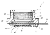
- 적어도 하나의 렌즈를 구비하는 렌즈배럴을 포함하는 하우징 ;상기 하우징에 배치되는 적어도 하나의 IR필터 ;상기 하우징에 배치되고, 상부면에 적어도 하나의 보강재가 적층되고, 적어도 하나의 수동소자가 탑재되는 기판; 및상기 기판의 일측단에 개구된 윈도우부를 통하여 결상영역이 외부노출되도록 상기 기판의 하부면에 결합되는 이미지 센서;를 포함하는 카메라 모듈 패키지.
- 제1항에 있어서,상기 보강재는 상기 기판의 상부면에 적층되는 커버레이층과 접착제층을 매개로 하여 접착되는 폴리이미드층으로 구비됨을 특징으로 하는 카메라 모듈 패키지.
- 제1항에 있어서,상기 보강재에는 상기 기판의 상부면에 외부노출되도록 패턴인쇄된 도금패턴과 솔더를 매개로 수동소자가 탑재되는 단자홀을 구비함을 특징으로 하는 카메라 모듈 패키지.
- 제3항에 있어서,상기 단자홀의 깊이는 상기 기판의 도금패턴에 솔더를 묻히는 솔더 마스킹 공정시 상기 단자홀내에 솔더가 채워질 수 있는 크기를 갖도록 상기 보강재의 형성두께를 가변시켜 조절함을 특징으로 하는 카메라 모듈 패키지.
Priority Applications (4)
| Application Number | Priority Date | Filing Date | Title |
|---|---|---|---|
| KR1020060038267A KR20070105723A (ko) | 2006-04-27 | 2006-04-27 | 카메라 모듈 패키지 |
| US11/790,664 US8199250B2 (en) | 2006-04-27 | 2007-04-26 | Camera module package |
| GB0708074A GB2437646B (en) | 2006-04-27 | 2007-04-26 | Camera module package |
| CNB2007101047626A CN100515039C (zh) | 2006-04-27 | 2007-04-26 | 相机模块封装 |
Applications Claiming Priority (1)
| Application Number | Priority Date | Filing Date | Title |
|---|---|---|---|
| KR1020060038267A KR20070105723A (ko) | 2006-04-27 | 2006-04-27 | 카메라 모듈 패키지 |
Publications (1)
| Publication Number | Publication Date |
|---|---|
| KR20070105723A true KR20070105723A (ko) | 2007-10-31 |
Family
ID=38170719
Family Applications (1)
| Application Number | Title | Priority Date | Filing Date |
|---|---|---|---|
| KR1020060038267A Ceased KR20070105723A (ko) | 2006-04-27 | 2006-04-27 | 카메라 모듈 패키지 |
Country Status (4)
| Country | Link |
|---|---|
| US (1) | US8199250B2 (ko) |
| KR (1) | KR20070105723A (ko) |
| CN (1) | CN100515039C (ko) |
| GB (1) | GB2437646B (ko) |
Cited By (5)
| Publication number | Priority date | Publication date | Assignee | Title |
|---|---|---|---|---|
| KR100902379B1 (ko) * | 2007-11-05 | 2009-06-11 | 삼성전기주식회사 | 인쇄회로기판과 그 제조 방법, 그리고 이를 포함하는카메라 모듈과 그 제조방법 |
| KR100910772B1 (ko) * | 2005-07-05 | 2009-08-04 | 삼성테크윈 주식회사 | 이미지 센서용 플립칩 패키지 및 이를 구비한 컴팩트카메라 모듈 |
| KR101044121B1 (ko) * | 2009-08-26 | 2011-06-28 | 삼성전기주식회사 | 카메라모듈 |
| KR20150076837A (ko) * | 2013-12-27 | 2015-07-07 | 세메스 주식회사 | 공정 챔버 및 이를 포함하는 기판 처리 장치 |
| KR20160015632A (ko) * | 2014-07-31 | 2016-02-15 | 엘지이노텍 주식회사 | 렌즈 배럴 및 이를 포함한 카메라 모듈 |
Families Citing this family (25)
| Publication number | Priority date | Publication date | Assignee | Title |
|---|---|---|---|---|
| KR100691157B1 (ko) * | 2005-04-07 | 2007-03-09 | 삼성전기주식회사 | 포커싱 무조정형 카메라 모듈 |
| CN100561736C (zh) * | 2007-05-25 | 2009-11-18 | 鸿富锦精密工业(深圳)有限公司 | 影像感测器封装结构及其应用的成像模组 |
| KR100950914B1 (ko) * | 2008-08-13 | 2010-04-01 | 삼성전기주식회사 | 카메라 모듈 |
| DE102008047088B4 (de) * | 2008-09-12 | 2019-05-29 | Jabil Circuit Inc. | Kamera-Modul für ein Mobiltelefon |
| JP5422484B2 (ja) * | 2010-05-20 | 2014-02-19 | 株式会社東芝 | カメラモジュール |
| KR101175869B1 (ko) * | 2010-08-18 | 2012-08-21 | 삼성전기주식회사 | 카메라 모듈 |
| CN102231382B (zh) * | 2011-06-17 | 2013-01-23 | 瑞声声学科技(深圳)有限公司 | 图像传感器的陶瓷封装及其封装方法 |
| KR20130057090A (ko) * | 2011-11-23 | 2013-05-31 | 엘지이노텍 주식회사 | 카메라 모듈 |
| KR20150118591A (ko) * | 2012-03-30 | 2015-10-23 | 삼성전기주식회사 | 카메라 모듈 |
| CN103594428B (zh) * | 2012-08-16 | 2017-10-24 | 三赢科技(深圳)有限公司 | 影像感测器模组及取像模组 |
| CN103594427A (zh) * | 2012-08-16 | 2014-02-19 | 鸿富锦精密工业(深圳)有限公司 | 影像感测器模组及取像模组 |
| CN103594426A (zh) * | 2012-08-16 | 2014-02-19 | 鸿富锦精密工业(深圳)有限公司 | 影像感测器模组及取像模组 |
| TW201421987A (zh) * | 2012-11-19 | 2014-06-01 | Hon Hai Prec Ind Co Ltd | 影像感測器模組及取像模組 |
| CN103065990A (zh) * | 2012-12-12 | 2013-04-24 | 山西国惠光电科技有限公司 | 一种晶圆级倒装互联方法 |
| CN104319264A (zh) * | 2014-10-14 | 2015-01-28 | 江西盛泰光学有限公司 | 一种玻璃上芯片封装摄像头模组 |
| KR102310996B1 (ko) * | 2014-12-30 | 2021-10-08 | 엘지이노텍 주식회사 | 렌즈 구동장치 및 이를 포함하는 카메라 모듈 |
| KR102406627B1 (ko) * | 2015-10-21 | 2022-06-08 | 엘지이노텍 주식회사 | 카메라 모듈 |
| CN106817522A (zh) * | 2015-12-01 | 2017-06-09 | 安徽昌硕光电子科技有限公司 | 摄像模块的结构 |
| US10466501B2 (en) * | 2016-05-26 | 2019-11-05 | Ams Sensors Singapore Pte. Ltd. | Optoelectronic modules including an optical system tilted with respect to a focal plane |
| CN207010790U (zh) * | 2017-04-17 | 2018-02-13 | 三赢科技(深圳)有限公司 | 成像模组 |
| CN110876002B (zh) * | 2018-08-31 | 2021-07-20 | 三赢科技(深圳)有限公司 | 摄像装置 |
| JP7686365B2 (ja) * | 2018-11-20 | 2025-06-02 | キヤノン株式会社 | 電子部品および機器 |
| US20200236254A1 (en) * | 2019-01-23 | 2020-07-23 | Black Seasme International Holding Limited | Camera system with reduced alignment shift |
| KR20210156013A (ko) * | 2020-06-17 | 2021-12-24 | 엘지이노텍 주식회사 | 카메라 모듈 및 광학기기 |
| EP3988983B1 (en) * | 2020-10-23 | 2024-08-14 | Magna Electronics Sweden AB | Camera assembly comprising a rotation blocking pin |
Family Cites Families (18)
| Publication number | Priority date | Publication date | Assignee | Title |
|---|---|---|---|---|
| JP3887162B2 (ja) * | 2000-10-19 | 2007-02-28 | 富士通株式会社 | 撮像用半導体装置 |
| US6949808B2 (en) * | 2001-11-30 | 2005-09-27 | Matsushita Electric Industrial Co., Ltd. | Solid-state imaging apparatus and manufacturing method thereof |
| JP2003244508A (ja) | 2002-02-21 | 2003-08-29 | Seiko Precision Inc | 固体撮像装置 |
| JP2003319216A (ja) | 2002-04-18 | 2003-11-07 | Shinko Electric Ind Co Ltd | 撮像装置 |
| KR100718421B1 (ko) * | 2002-06-28 | 2007-05-14 | 교세라 가부시키가이샤 | 소형 모듈 카메라, 카메라 모듈, 카메라 모듈 제조 방법 및 촬상 소자의 패키징 방법 |
| TW558064U (en) * | 2002-09-23 | 2003-10-11 | Ist Internat Semiconductor Tec | Thin type camera module |
| JP4204368B2 (ja) * | 2003-03-28 | 2009-01-07 | シャープ株式会社 | 光学装置用モジュール及び光学装置用モジュールの製造方法 |
| US20060234767A1 (en) * | 2003-04-22 | 2006-10-19 | Takuo Nishikawa | Imaging device and mobile terminal using this imaging device |
| DE10344768B3 (de) | 2003-09-26 | 2005-08-18 | Siemens Ag | Optisches Modul mit federndem Element zwischen Linsenhalter und Schaltungsträger und optisches System |
| TWI296154B (en) * | 2004-01-27 | 2008-04-21 | Casio Computer Co Ltd | Optical sensor module |
| JP4236594B2 (ja) * | 2004-01-27 | 2009-03-11 | シャープ株式会社 | 光学装置用モジュール及び光学装置用モジュールの製造方法 |
| US6979902B2 (en) * | 2004-03-10 | 2005-12-27 | Micron Technology, Inc. | Chip size image sensor camera module |
| US7714931B2 (en) * | 2004-06-25 | 2010-05-11 | Flextronics International Usa, Inc. | System and method for mounting an image capture device on a flexible substrate |
| KR100674833B1 (ko) * | 2005-02-16 | 2007-01-26 | 삼성전기주식회사 | 카메라 모듈 |
| KR100721163B1 (ko) * | 2005-09-27 | 2007-05-23 | 삼성전기주식회사 | 이미지 센서 모듈과 이를 이용한 카메라 모듈 및 카메라모듈의 제조방법 |
| KR100704980B1 (ko) * | 2005-11-28 | 2007-04-09 | 삼성전기주식회사 | 카메라 모듈 패키지 |
| KR100744925B1 (ko) * | 2005-12-27 | 2007-08-01 | 삼성전기주식회사 | 카메라 모듈 패키지 |
| KR100770690B1 (ko) * | 2006-03-15 | 2007-10-29 | 삼성전기주식회사 | 카메라모듈 패키지 |
-
2006
- 2006-04-27 KR KR1020060038267A patent/KR20070105723A/ko not_active Ceased
-
2007
- 2007-04-26 US US11/790,664 patent/US8199250B2/en not_active Expired - Fee Related
- 2007-04-26 CN CNB2007101047626A patent/CN100515039C/zh not_active Expired - Fee Related
- 2007-04-26 GB GB0708074A patent/GB2437646B/en not_active Expired - Fee Related
Cited By (5)
| Publication number | Priority date | Publication date | Assignee | Title |
|---|---|---|---|---|
| KR100910772B1 (ko) * | 2005-07-05 | 2009-08-04 | 삼성테크윈 주식회사 | 이미지 센서용 플립칩 패키지 및 이를 구비한 컴팩트카메라 모듈 |
| KR100902379B1 (ko) * | 2007-11-05 | 2009-06-11 | 삼성전기주식회사 | 인쇄회로기판과 그 제조 방법, 그리고 이를 포함하는카메라 모듈과 그 제조방법 |
| KR101044121B1 (ko) * | 2009-08-26 | 2011-06-28 | 삼성전기주식회사 | 카메라모듈 |
| KR20150076837A (ko) * | 2013-12-27 | 2015-07-07 | 세메스 주식회사 | 공정 챔버 및 이를 포함하는 기판 처리 장치 |
| KR20160015632A (ko) * | 2014-07-31 | 2016-02-15 | 엘지이노텍 주식회사 | 렌즈 배럴 및 이를 포함한 카메라 모듈 |
Also Published As
| Publication number | Publication date |
|---|---|
| GB2437646B (en) | 2009-03-11 |
| CN101064776A (zh) | 2007-10-31 |
| US20070253697A1 (en) | 2007-11-01 |
| GB2437646A (en) | 2007-10-31 |
| GB0708074D0 (en) | 2007-06-06 |
| CN100515039C (zh) | 2009-07-15 |
| US8199250B2 (en) | 2012-06-12 |
Similar Documents
| Publication | Publication Date | Title |
|---|---|---|
| KR20070105723A (ko) | 카메라 모듈 패키지 | |
| KR100718421B1 (ko) | 소형 모듈 카메라, 카메라 모듈, 카메라 모듈 제조 방법 및 촬상 소자의 패키징 방법 | |
| US7515817B2 (en) | Camera module | |
| KR100867523B1 (ko) | 카메라 모듈 패키지 | |
| JP4372143B2 (ja) | カメラモジュールパッケージ | |
| JP5982380B2 (ja) | 撮像素子モジュール及びその製造方法 | |
| KR20070068607A (ko) | 카메라 모듈 패키지 | |
| KR100860308B1 (ko) | 카메라 모듈 패키지 및 그 제조방법 | |
| KR100780204B1 (ko) | 접지용 더미기판을 갖는 카메라 모듈 | |
| CN101853846A (zh) | 半导体模块及搭载有该模块的照相机模块 | |
| CN204669479U (zh) | 摄像头模块 | |
| US20040256687A1 (en) | Optical module, method of manufacturing the same, and electronic instrument | |
| US9013621B2 (en) | Image sensor module and camera module using same | |
| WO2012029318A1 (ja) | 素子搭載用基板および光学モジュール | |
| KR100835719B1 (ko) | 센서 내장형 이미지센서 모듈 및 이를 이용한 카메라 모듈패키지 | |
| KR100818486B1 (ko) | 카메라 모듈 패키지 | |
| KR101139368B1 (ko) | 카메라 모듈 | |
| KR20080051449A (ko) | 카메라 모듈 패키지 및 그 조립방법 | |
| KR20080051445A (ko) | 이미지센서 모듈과 그 제조 방법 및 이를 포함하는 카메라모듈 | |
| KR100674839B1 (ko) | 카메라 모듈 | |
| TWI728737B (zh) | 攝像模組封裝結構 | |
| KR100674852B1 (ko) | 카메라 모듈 패키지 | |
| KR100741828B1 (ko) | 카메라모듈 패키지 및 그 제조방법 | |
| KR100803275B1 (ko) | 카메라장치 및 그 제조방법 | |
| JP2008166521A (ja) | 固体撮像装置 |
Legal Events
| Date | Code | Title | Description |
|---|---|---|---|
| A201 | Request for examination | ||
| PA0109 | Patent application |
Patent event code: PA01091R01D Comment text: Patent Application Patent event date: 20060427 |
|
| PA0201 | Request for examination | ||
| E902 | Notification of reason for refusal | ||
| PE0902 | Notice of grounds for rejection |
Comment text: Notification of reason for refusal Patent event date: 20070628 Patent event code: PE09021S01D |
|
| E601 | Decision to refuse application | ||
| PE0601 | Decision on rejection of patent |
Patent event date: 20070929 Comment text: Decision to Refuse Application Patent event code: PE06012S01D Patent event date: 20070628 Comment text: Notification of reason for refusal Patent event code: PE06011S01I |
|
| PG1501 | Laying open of application |