KR20070044432A - Organic EL display - Google Patents
Organic EL display Download PDFInfo
- Publication number
- KR20070044432A KR20070044432A KR1020077000798A KR20077000798A KR20070044432A KR 20070044432 A KR20070044432 A KR 20070044432A KR 1020077000798 A KR1020077000798 A KR 1020077000798A KR 20077000798 A KR20077000798 A KR 20077000798A KR 20070044432 A KR20070044432 A KR 20070044432A
- Authority
- KR
- South Korea
- Prior art keywords
- light
- organic
- light emitting
- reflecting member
- wavelength
- Prior art date
- Legal status (The legal status is an assumption and is not a legal conclusion. Google has not performed a legal analysis and makes no representation as to the accuracy of the status listed.)
- Withdrawn
Links
Images


Classifications
-
- H—ELECTRICITY
- H10—SEMICONDUCTOR DEVICES; ELECTRIC SOLID-STATE DEVICES NOT OTHERWISE PROVIDED FOR
- H10K—ORGANIC ELECTRIC SOLID-STATE DEVICES
- H10K59/00—Integrated devices, or assemblies of multiple devices, comprising at least one organic light-emitting element covered by group H10K50/00
- H10K59/30—Devices specially adapted for multicolour light emission
- H10K59/38—Devices specially adapted for multicolour light emission comprising colour filters or colour changing media [CCM]
-
- H—ELECTRICITY
- H05—ELECTRIC TECHNIQUES NOT OTHERWISE PROVIDED FOR
- H05B—ELECTRIC HEATING; ELECTRIC LIGHT SOURCES NOT OTHERWISE PROVIDED FOR; CIRCUIT ARRANGEMENTS FOR ELECTRIC LIGHT SOURCES, IN GENERAL
- H05B33/00—Electroluminescent light sources
- H05B33/12—Light sources with substantially two-dimensional radiating surfaces
- H05B33/22—Light sources with substantially two-dimensional radiating surfaces characterised by the chemical or physical composition or the arrangement of auxiliary dielectric or reflective layers
- H05B33/24—Light sources with substantially two-dimensional radiating surfaces characterised by the chemical or physical composition or the arrangement of auxiliary dielectric or reflective layers of metallic reflective layers
-
- H—ELECTRICITY
- H05—ELECTRIC TECHNIQUES NOT OTHERWISE PROVIDED FOR
- H05B—ELECTRIC HEATING; ELECTRIC LIGHT SOURCES NOT OTHERWISE PROVIDED FOR; CIRCUIT ARRANGEMENTS FOR ELECTRIC LIGHT SOURCES, IN GENERAL
- H05B33/00—Electroluminescent light sources
- H05B33/12—Light sources with substantially two-dimensional radiating surfaces
- H05B33/14—Light sources with substantially two-dimensional radiating surfaces characterised by the chemical or physical composition or the arrangement of the electroluminescent material, or by the simultaneous addition of the electroluminescent material in or onto the light source
-
- H—ELECTRICITY
- H10—SEMICONDUCTOR DEVICES; ELECTRIC SOLID-STATE DEVICES NOT OTHERWISE PROVIDED FOR
- H10K—ORGANIC ELECTRIC SOLID-STATE DEVICES
- H10K50/00—Organic light-emitting devices
- H10K50/80—Constructional details
- H10K50/85—Arrangements for extracting light from the devices
- H10K50/852—Arrangements for extracting light from the devices comprising a resonant cavity structure, e.g. Bragg reflector pair
-
- H—ELECTRICITY
- H10—SEMICONDUCTOR DEVICES; ELECTRIC SOLID-STATE DEVICES NOT OTHERWISE PROVIDED FOR
- H10K—ORGANIC ELECTRIC SOLID-STATE DEVICES
- H10K50/00—Organic light-emitting devices
- H10K50/10—OLEDs or polymer light-emitting diodes [PLED]
- H10K50/11—OLEDs or polymer light-emitting diodes [PLED] characterised by the electroluminescent [EL] layers
- H10K50/125—OLEDs or polymer light-emitting diodes [PLED] characterised by the electroluminescent [EL] layers specially adapted for multicolour light emission, e.g. for emitting white light
-
- H—ELECTRICITY
- H10—SEMICONDUCTOR DEVICES; ELECTRIC SOLID-STATE DEVICES NOT OTHERWISE PROVIDED FOR
- H10K—ORGANIC ELECTRIC SOLID-STATE DEVICES
- H10K59/00—Integrated devices, or assemblies of multiple devices, comprising at least one organic light-emitting element covered by group H10K50/00
- H10K59/80—Constructional details
- H10K59/875—Arrangements for extracting light from the devices
- H10K59/876—Arrangements for extracting light from the devices comprising a resonant cavity structure, e.g. Bragg reflector pair
-
- H—ELECTRICITY
- H10—SEMICONDUCTOR DEVICES; ELECTRIC SOLID-STATE DEVICES NOT OTHERWISE PROVIDED FOR
- H10K—ORGANIC ELECTRIC SOLID-STATE DEVICES
- H10K85/00—Organic materials used in the body or electrodes of devices covered by this subclass
- H10K85/30—Coordination compounds
- H10K85/321—Metal complexes comprising a group IIIA element, e.g. Tris (8-hydroxyquinoline) gallium [Gaq3]
- H10K85/324—Metal complexes comprising a group IIIA element, e.g. Tris (8-hydroxyquinoline) gallium [Gaq3] comprising aluminium, e.g. Alq3
-
- H—ELECTRICITY
- H10—SEMICONDUCTOR DEVICES; ELECTRIC SOLID-STATE DEVICES NOT OTHERWISE PROVIDED FOR
- H10K—ORGANIC ELECTRIC SOLID-STATE DEVICES
- H10K85/00—Organic materials used in the body or electrodes of devices covered by this subclass
- H10K85/60—Organic compounds having low molecular weight
- H10K85/615—Polycyclic condensed aromatic hydrocarbons, e.g. anthracene
-
- H—ELECTRICITY
- H10—SEMICONDUCTOR DEVICES; ELECTRIC SOLID-STATE DEVICES NOT OTHERWISE PROVIDED FOR
- H10K—ORGANIC ELECTRIC SOLID-STATE DEVICES
- H10K85/00—Organic materials used in the body or electrodes of devices covered by this subclass
- H10K85/60—Organic compounds having low molecular weight
- H10K85/631—Amine compounds having at least two aryl rest on at least one amine-nitrogen atom, e.g. triphenylamine
Landscapes
- Physics & Mathematics (AREA)
- Optics & Photonics (AREA)
- Electroluminescent Light Sources (AREA)
Abstract
발광 피크 파장 λ1이 400 ㎚ 내지 500 ㎚ 범위인 빛을 발하는 유기 발광 매체(4), 상기 유기 발광 매체(4)를 사이에 협지하는 제1 광 반사 부재(2) 및 제2 광 반사 부재(5b)를 포함하는 유기 전계 발광 소자, 및 상기 유기 전계 발광 소자가 발하는 빛을 흡수하고 상이한 파장의 빛을 발하는, 여기 스펙트럼에 있어서의 400 ㎚ 내지 500 ㎚ 범위 내에서 최대값이 되는 파장이 λ2인 형광 변환부(7)를 갖고, 상기 유기 발광 매체(4)가 발하는 빛이 제1 광 반사 부재(2) 및 제2 광 반사 부재(5b) 사이에서 간섭되어 파장 λ1보다도 파장 λ2에 가까운 파장 λ3의 발광 성분이 강화되고, 유기 전계 발광 소자로부터 발해지는, 유기 EL 표시 장치. An organic light emitting medium 4 emitting light having an emission peak wavelength λ1 in a range of 400 nm to 500 nm, a first light reflecting member 2 and a second light reflecting member 5b sandwiching the organic light emitting medium 4 therebetween And an fluorescence having a maximum wavelength within a range of 400 nm to 500 nm in an excitation spectrum that absorbs light emitted by the organic electroluminescent device and emits light having a different wavelength. The light having the conversion unit 7 and the light emitted from the organic light emitting medium 4 is interfered between the first light reflecting member 2 and the second light reflecting member 5b and has a wavelength λ 3 closer to the wavelength λ 2 than the wavelength λ 1. An organic EL display device in which a light emitting component is enhanced and is emitted from an organic electroluminescent element.
유기 전계 발광 표시 장치, 유기 발광 매체, 발광 피크 파장, 색 변환 부재 Organic electroluminescent display, organic light emitting medium, peak emission wavelength, color conversion member
Description
본 발명은 유기 전계 발광(EL) 표시 장치, 특히 무기 형광체를 이용한 유기 EL 표시 장치에 관한 것이다. The present invention relates to an organic electroluminescent (EL) display device, in particular an organic EL display device using an inorganic phosphor.
유기 EL 표시 장치는 대향하는 전극 사이에 유기 발광 매체를 협지한 유기 EL 소자로 구성되어 있다. 유기 EL 소자의 양 전극 사이에 전압을 인가하면, 한쪽 전극으로부터 주입된 전자와 다른 쪽 전극으로부터 주입된 홀이 유기 발광 매체에서 재결합된다. 유기 발광 매체 중의 유기 발광 분자는 재결합 에너지에 의해 일단 여기 상태가 되고, 그 후, 여기 상태로부터 기저 상태로 되돌아간다. 이 때에 방출되는 에너지를 빛으로 취출함으로써 유기 EL 소자가 발광한다. The organic EL display device is composed of an organic EL element in which an organic light emitting medium is sandwiched between opposing electrodes. When a voltage is applied between both electrodes of the organic EL element, electrons injected from one electrode and holes injected from the other electrode are recombined in the organic light emitting medium. The organic light emitting molecules in the organic light emitting medium are once excited by the recombination energy, and then return from the excited state to the ground state. At this time, the organic EL element emits light by extracting energy emitted by light.
유기 EL 소자가 청색광을 발할 때, 형광 변환체에 의해 녹색광 및 적색광으로 변환하여 풀 컬러화를 실현하고 있다. 최근 들어 형광 변환체로서 고효율이면서 내구성이 높은 재료가, 유기 형광체뿐만 아니라 무기 형광체에도 발견되었다(예를 들면, 미국 특허 제6,501,091호). When the organic EL element emits blue light, full colorization is realized by converting it into green light and red light by the fluorescent converter. Recently, a highly efficient and durable material has been found as a fluorescent converter not only in organic phosphors but also in inorganic phosphors (for example, US Pat. No. 6,501,091).
새롭게 발견된 무기 형광체의 여기 파장은 460 ㎚ 이하의 단파장인 경우가 많다. 따라서, 이러한 무기 형광체를 이용한 형광 변환부를 여기하기 위해서는 청색계 유기 발광 매체의 피크 파장도 짧은 것을 채용할 필요가 있었다. 그러나, 피 크 파장이 짧은 청색계 발광 매체를 이용하면, 연속 구동 수명이 짧고, 발광 효율이 나쁜 등의 문제가 있었다. The excitation wavelength of the newly discovered inorganic phosphor is often short wavelength of 460 nm or less. Therefore, in order to excite the fluorescence conversion unit using such an inorganic phosphor, it was necessary to adopt a short peak wavelength of the blue organic light emitting medium. However, when a blue light emitting medium having a short peak wavelength is used, there are problems such as short continuous driving life and poor luminous efficiency.
본 발명의 목적은 고효율이고 연속 구동 수명이 긴 유기 EL 표시 장치를 제공하는 것이다. An object of the present invention is to provide an organic EL display device having a high efficiency and a long continuous driving life.
본 발명자들은 예의 연구한 결과, 형광 변환부의 여기 파장과 상이한 발광 파장을 나타내는 유기 발광 매체에 있어서, 광 간섭 효과를 이용하여, 형광 변환부의 형광 파장에 일치시키도록 유기 발광 매체의 발광을 증강시킬 수 있음을 발견하여 본 발명을 완성시켰다.As a result of intensive studies, the present inventors can enhance the light emission of an organic light emitting medium so as to match the fluorescence wavelength of the fluorescence conversion part by using an optical interference effect in an organic light emitting medium having a light emission wavelength different from the excitation wavelength of the fluorescence conversion part. The present invention was completed.
본 발명에 따르면, 이하의 유기 EL 표시 장치가 제공된다.According to the present invention, the following organic EL display device is provided.
1. 발광 피크 파장 λ1이 400 ㎚ 내지 500 ㎚의 범위인 빛을 발하는 유기 발광 매체,1. an organic light emitting medium that emits light in which the emission peak wavelength λ1 is in the range of 400 nm to 500 nm,
상기 유기 발광 매체를 사이에 협지하는 제1 광 반사 부재 및 제2 광 반사 부재를 포함하는 유기 EL 소자, 및An organic EL element comprising a first light reflecting member and a second light reflecting member sandwiching the organic light emitting medium therebetween, and
상기 유기 EL 소자가 발하는 빛을 흡수하여 상이한 파장의 빛을 발하는, 여기 스펙트럼에서의 400 ㎚ 내지 500 ㎚ 범위 내에서 최대값이 되는 파장이 λ2인 형광 변환부를 갖고, Having a fluorescence conversion portion having a wavelength of
상기 유기 발광 매체가 발하는 빛이 제1 광 반사 부재 및 제2 광 반사 부재 사이에서 간섭되어, 파장 λ1보다도 파장 λ2에 가까운 파장 λ3의 발광 성분이 강화되고 유기 EL 소자로부터 발해지는 유기 EL 표시 장치. An organic EL display device in which light emitted from the organic light emitting medium interferes between the first light reflecting member and the second light reflecting member, so that a light emitting component having a
2. 상기 형광 변환부가 무기 형광체를 포함하는 1에 기재된 유기 EL 표시 장치. 2. The organic EL display device according to 1, wherein the fluorescence conversion unit contains an inorganic phosphor.
3. 발광 피크 파장 λb를 갖는 청색광을 발하는 유기 발광 매체를 포함하는 제1 유기 EL 소자를 갖는 청색 화소;3. a blue pixel having a first organic EL element comprising an organic light emitting medium emitting blue light having an emission peak wavelength [lambda] b;
발광 피크 파장 λb를 갖는 청색광을 발하는 유기 발광 매체, An organic light emitting medium emitting blue light having an emission peak wavelength lambda b,
상기 유기 발광 매체를 사이에 협지하고, 제1 광학 막두께를 형성하는 제1 광 반사 부재 및 제2 광 반사 부재를 포함하는 제2 유기 EL 소자, 및A second organic EL element comprising a first light reflecting member and a second light reflecting member sandwiching the organic light emitting medium and forming a first optical film thickness, and
상기 제2 유기 EL 소자가 발하는 청색광을 흡수하여 녹색광을 발하는, 여기 스펙트럼의 최대 피크 파장이 λg인 녹색 형광 변환부를 갖고, It has a green fluorescence conversion part whose maximum peak wavelength of an excitation spectrum is (lambda) g which absorbs the blue light emitted by the said 2nd organic electroluminescent element, and emits green light,
상기 유기 발광 매체가 발하는 빛이 제1 광 반사 부재 및 제2 광 반사 부재 사이에서 간섭되어, 파장 λb보다도 파장 λg에 가까운 파장 λb1의 발광 성분이 강화되고 제2 유기 EL 소자로부터 발해지는, 녹색 화소; 및The green pixel which the light emitted from the said organic light emitting medium interferes between a 1st light reflecting member and a 2nd light reflecting member, and the light emission component of wavelength (lambda) b1 which is closer to wavelength (lambda) g than wavelength (lambda) b is reinforced and emitted from a 2nd organic electroluminescent element. ; And
발광 피크 파장 λb를 갖는 청색광을 발하는 유기 발광 매체, An organic light emitting medium emitting blue light having an emission peak wavelength lambda b,
상기 유기 발광 매체를 사이에 협지하고, 제2 광학 막두께를 형성하는 제1 광 반사 부재 및 제2 광 반사 부재를 포함하는 제3 유기 EL 소자, 및A third organic EL element comprising a first light reflecting member and a second light reflecting member sandwiching the organic light emitting medium therebetween and forming a second optical film thickness, and
상기 제3 유기 EL 소자가 발하는 청색광을 흡수하여 적색광을 발하는, 여기 스펙트럼의 최대 피크 파장이 λr인 적색 형광 변환부를 갖고, It has a red fluorescence conversion part whose maximum peak wavelength of an excitation spectrum is (lambda) r which absorbs the blue light emitted by the said 3rd organic electroluminescent element, and emits a red light,
상기 유기 발광 매체가 발하는 빛이 제1 광 반사 부재 및 제2 광 반사 부재 사이에서 간섭되어, 파장 λb보다도 파장 λr에 가까운 파장 λb2의 발광 성분이 강화되고 제3 유기 EL 소자로부터 발해지는, 적색 화소Light emitted from the organic light emitting medium interferes between the first light reflecting member and the second light reflecting member, so that the red light emitting component having a wavelength? B2 closer to the wavelength? R than the wavelength? B is enhanced and emitted from the third organic EL element.
를 갖는 유기 EL 표시 장치. An organic EL display device having.
4. 상기 적색 형광 변환부 및 상기 녹색 형광 변환부가 무기 형광체를 포함하는 3에 기재된 유기 EL 표시 장치. 4. The organic EL display device according to 3, wherein the red fluorescence conversion unit and the green fluorescence conversion unit contain an inorganic phosphor.
5. 상기 제1 광학 막두께를 형성하는 제1 광 반사 부재 및 제2 광 반사 부재 사이, 또는 상기 제2 광학 막두께를 형성하는 제1 광 반사 부재 및 제2 광 반사 부재 사이에 광학 막두께 조정층을 갖는 3에 기재된 유기 전계 발광 표시 장치. 5. Optical film thickness between a first light reflecting member and a second light reflecting member forming said first optical film thickness, or between a first light reflecting member and a second light reflecting member forming said second optical film thickness. The organic electroluminescent display device of 3 which has an adjustment layer.
6. 발광 피크 파장 λb를 갖는 청색광을 발하는 유기 발광 매체, 및 6. an organic light emitting medium emitting blue light having an emission peak wavelength [lambda] b, and
상기 유기 발광 매체를 사이에 협지하고, 제1 광학 막두께를 형성하는 제1 광 반사 부재 및 제2 광 반사 부재를 포함하는 제1 유기 전계 발광 소자를 갖고, It has a 1st organic electroluminescent element containing the said 1st light reflection member and a 2nd light reflection member which sandwich the said organic light emitting medium, and form a 1st optical film thickness,
상기 유기 발광 매체가 발하는 빛이 제1 광 반사 부재 및 제2 광 반사 부재 사이에서 간섭되어, 청색의 발광 성분이 강화되고 제1 유기 전계 발광 소자로부터 발해지는, 청색 화소; Blue pixels emitted from the organic light emitting medium by interference between the first light reflecting member and the second light reflecting member so that the blue light emitting component is enhanced and emitted from the first organic electroluminescent element;
발광 피크 파장 λb를 갖는 청색광을 발하는 유기 발광 매체, An organic light emitting medium emitting blue light having an emission peak wavelength lambda b,
상기 유기 발광 매체를 사이에 협지하고, 제2 광학 막두께를 형성하는 제1 광 반사 부재 및 제2 광 반사 부재를 포함하는 제2 유기 전계 발광 소자, 및A second organic electroluminescent element comprising a first light reflecting member and a second light reflecting member sandwiching the organic light emitting medium and forming a second optical film thickness, and
상기 제2 유기 전계 발광 소자가 발하는 청색광을 흡수하여 녹색광을 발하는, 여기 스펙트럼의 최대 피크 파장이 λg인 녹색 형광 변환부를 갖고, It has a green fluorescence conversion part whose maximum peak wavelength of an excitation spectrum is (lambda) g which absorbs the blue light emitted by the said 2nd organic electroluminescent element, and emits green light,
상기 유기 발광 매체가 발하는 빛이 제1 광 반사 부재 및 제2 광 반사 부재 사이에서 간섭되어, 파장 λb보다도 파장 λg에 가까운 파장 λb1의 발광 성분이 강화되고 제2 유기 전계 발광 소자로부터 발해지는, 녹색 화소; 및Green light emitted from the second organic electroluminescent element by the light emitted from the organic light emitting medium interferes between the first light reflecting member and the second light reflecting member so that the light emitting component having the wavelength λ b1 closer to the wavelength λ g than the wavelength λ b is strengthened. Pixels; And
발광 피크 파장 λb를 갖는 청색광을 발하는 유기 발광 매체, An organic light emitting medium emitting blue light having an emission peak wavelength lambda b,
상기 유기 발광 매체를 사이에 협지하고, 제3 광학 막두께를 형성하는 제1 광 반사 부재 및 제2 광 반사 부재를 포함하는 제3 유기 전계 발광 소자, 및A third organic electroluminescent element comprising a first light reflecting member and a second light reflecting member sandwiching the organic light emitting medium and forming a third optical film thickness, and
상기 제3 유기 전계 발광 소자가 발하는 청색광을 흡수하여 적색광을 발하는, 여기 스펙트럼의 최대 피크 파장이 λr인 적색 형광 변환부를 갖고, A red fluorescence conversion portion having a maximum peak wavelength of λ r for absorbing blue light emitted by the third organic electroluminescent element and emitting red light,
상기 유기 발광 매체가 발하는 빛이 제1 광 반사 부재 및 제2 광 반사 부재 사이에서 간섭되어, 파장 λb보다도 파장 λr에 가까운 파장 λb2의 발광 성분이 강화되고 제3 유기 전계 발광 소자로부터 발해지는, 적색 화소Light emitted from the organic light emitting medium interferes between the first light reflecting member and the second light reflecting member, so that the light emitting component having a wavelength lambda b2 closer to the wavelength lambda r than the wavelength lambda b is enhanced and emitted from the third organic electroluminescent element. Pixel
를 갖는 유기 전계 발광 표시 장치. An organic light emitting display device having a.
7. 상기 적색 형광 변환부 및 상기 녹색 형광 변환부가 무기 형광체를 포함하는 6에 기재된 유기 전계 발광 표시 장치. 7. The organic electroluminescent display device according to 6, wherein the red fluorescence conversion unit and the green fluorescence conversion unit contain an inorganic phosphor.
8. 상기 제2 광학 막두께를 형성하는 제1 광 반사 부재 및 제2 광 반사 부재 사이에 제1 광학 막두께 조정층을 갖고, 상기 제3 광학 막두께를 형성하는 제1 광 반사 부재 및 제2 광 반사 부재 사이에 제2 광학 막두께 조정층을 갖는 6에 기재된 유기 전계 발광 표시 장치. 8. A first light reflecting member and a first light reflecting member having a first optical film thickness adjusting layer between the first light reflecting member and the second light reflecting member for forming the second optical film thickness, and for forming the third optical film thickness. The organic electroluminescent display device of 6 which has a 2nd optical film thickness adjustment layer between 2 light reflection members.
9. 추가로 기판을 갖고, 빛을 기판과 반대측으로부터 취출하는 상부 에미션 타입인 1 내지 8 중 어느 하나에 기재된 유기 EL 표시 장치. 9. The organic EL display device according to any one of 1 to 8, which is a top emission type that further has a substrate and extracts light from the opposite side to the substrate.
10. 추가로 기판을 갖고, 빛을 기판측으로부터 취출하는 하부 에미션 타입인 1 내지 8 중 어느 하나에 기재된 유기 전계 발광 표시 장치. 10. The organic electroluminescence display device according to any one of 1 to 8, which is a lower emission type that further has a substrate and extracts light from the substrate side.
본 발명에 따르면, 고효율이고 연속 구동 수명이 긴 유기 EL 표시 장치를 제공할 수 있다. According to the present invention, an organic EL display device having a high efficiency and a long continuous driving life can be provided.
도 1은 본 발명의 유기 EL 표시 장치의 일 실시 형태를 나타내는 도면이다. BRIEF DESCRIPTION OF THE DRAWINGS It is a figure which shows one Embodiment of the organic electroluminescence display of this invention.
도 2a는 간섭 효과를 받기 전의, 유기 발광 매체의 발광 스펙트럼과 형광 변환부의 여기 스펙트럼을 나타내는 도면이다. 2A is a diagram showing an emission spectrum of an organic light emitting medium and an excitation spectrum of a fluorescence conversion unit before receiving an interference effect.
도 2b는 간섭 효과를 받은 후의, 유기 발광 매체의 발광 스펙트럼과 형광 변환부의 여기 스펙트럼을 나타내는 도면이다. It is a figure which shows the emission spectrum of an organic light emitting medium, and the excitation spectrum of a fluorescence conversion part after receiving an interference effect.
도 3은 본 발명의 유기 EL 표시 장치의 다른 실시 형태를 나타내는 도면이다.3 is a diagram showing another embodiment of the organic EL display device of the present invention.
도 4는 본 발명의 유기 EL 표시 장치의 다른 실시 형태를 나타내는 도면이다.4 is a diagram showing another embodiment of the organic EL display device of the present invention.
도 5는 본 발명의 유기 EL 표시 장치의 다른 실시 형태를 나타내는 도면이다. 5 is a diagram showing another embodiment of the organic EL display device of the present invention.
<발명을 실시하기 위한 최선의 형태>Best Mode for Carrying Out the Invention
[실시 형태 1]
도 1은 본 발명의 유기 EL 표시 장치의 일 실시 형태를 나타내는 도면이며, 기판(1) 상에 제1 반사성 전극(제1 광 반사 부재)(2), 유기 발광 매체(4),제2 반사성 전극(5), 고체 밀봉층(6) 및 형광 변환부(7)가 차례로 적층되어 있다. 반사성 전극(5)은 금속막(5b)(제2 광 반사 부재)과 투명 전극(5a)을 포함한다. 두 개의 반사성 전극(2, 5) 중 한쪽이 양극이고, 다른 쪽이 음극이 된다. 화살표는 광 취 출 방향을 나타낸다(상부 에미션 타입).1 is a view showing an embodiment of an organic EL display device of the present invention, wherein a first reflective electrode (first light reflecting member) 2, an organic
여기서, 제1 반사성 전극(2), 유기 발광 매체(4) 및 제2 반사성 전극(5)으로 유기 EL 소자가 구성된다. L은 유기 EL 소자의 반사성 전극(2, 5) 사이의 광학 막두께를 모식적으로 나타낸다. 광학 막두께는 후술하는 바와 같이 실제 막 두께와 굴절률의 곱이다. 유기 발광 매체(4)는 도 2a에 나타낸 바와 같이 발광 피크 파장 λ1을 갖는 발광 스펙트럼(A)의 청색광을 발한다. 또한, 도 2a에 나타낸 바와 같이 형광 변환부(7)의 여기 스펙트럼(B)의 최대 피크 파장은 (λ2)이다. Here, the organic EL element is composed of the first
다음으로, 이 유기 EL 표시 장치의 동작에 대하여 설명한다. Next, the operation of this organic EL display device will be described.
우선, 유기 발광 매체(4)로부터 도 2a에 나타내는 발광 피크 파장 λ1을 갖는 청색광이 발해진다. 이 청색광은 반사성 전극(2, 5) 사이를 반사를 반복하여 간섭됨으로써, 도 2b에 나타낸 바와 같이, 거의 파장 λ2과 동일 파장 λ3의 발광 성분이 강화된 발광 스펙트럼(A')을 갖는 빛이 소자 밖으로 취출된다.First, blue light having the emission peak wavelength λ1 shown in FIG. 2A is emitted from the organic
형광 변환부(7)는 소자로부터 파장 λ3이 강화된 빛을 받기 때문에 효율적으로 여기되고, 청색광을 변환한다. Since the
형광 변환부(7)는 유기 형광체일 수도 있고, 무기 형광체일 수도 있다. 그러나, 무기 형광체는 460 ㎚ 이하의 단파장인 경우가 많기 때문에, 이러한 무기 형광체와 피크 파장이 긴 청색 발광 매체를 조합하여 사용하는 장치에 있어서 본 발명은 효과적이다. The
유기 EL 소자는 반사성 전극(2)과 금속막(5b) 사이를 공진부로 하는 광 공진기 구조로 되어 있다. 이 공진기 구조에 의해, 유기 발광 매체(4)에서 발생한 빛 은 2개의 반사면(반사성 전극(2)과 금속막(5b)) 사이에서 반사를 반복하고, 하기 수학식 1을 만족시키는 파장 부근의 빛이 선택적으로 강하게 소자 밖으로 방출된다. The organic EL element has an optical resonator structure having a resonant portion between the
여기서, L은 공진부의 광학적 거리, λ는 빛의 파장, Φ는 2개의 반사 부재 계면에 있어서의 위상 시프트의 합, m은 0 이상의 정수를 나타낸다.Where L is the optical distance of the resonant portion,? Is the wavelength of light,? Is the sum of the phase shifts at the two reflective member interfaces, and m is an integer of 0 or more.
광학적 거리 L은 빛이 통과하는 매체의 굴절률 n과 실제의 기하학적 거리 LR과의 곱이다. L은 다음과 같이 하여 구한다. The optical distance L is the product of the refractive index n of the medium through which light passes and the actual geometric distance L R. L is calculated as follows.
유기 발광 매체(4)를 구성하는 재료 단독의 박막을 지지 기판 상에 제조한다. 다음으로 엘립소미터 등의 장치를 이용하여, 제조한 박막 시료의 광학 측정을 행하고, 재료의 굴절률 n을 구한다. A thin film of the material constituting the organic
한편, 도 1에 있어서, 발명을 이해하여 쉽게 하기 위해, 2개의 전극(2, 5)에 끼워져 있는 것은 유기 발광 매체(4)뿐이지만, 후술하는 바와 같이, 통상적으로 전자 주입층, 전자 수송층, 정공 주입층, 정공 수송층 등을 추가로 포함하여 전체적으로 유기층을 형성한다. 반사 부재 사이에 복수의 층이 있을 때, L은 각층의 막 두께 d와 굴절률 n의 곱을 계산하고, 그 총합을 구함으로써 얻어진다. In FIG. 1, only the organic
Φ는 다음과 같이 하여 구한다. Φ is obtained as follows.
위상 시프트의 합 Φ는 다음 수학식으로 표시된다.The sum phi of the phase shift is expressed by the following equation.
여기서 Φ1는 다음과 같이 구한다. 우선, 지지 기판 상에 목적으로 하는 반사성 전극(2)를 형성하고, 엘립소미터 등의 장치를 이용하여, 제조한 박막 시료의 광학 측정을 행하고, 재료의 굴절률 n0과 감쇠 계수 k0을 구한다. 다음으로, Φ1는 하기 수학식 3으로 계산할 수 있다. 여기서, n1은 반사성 전극(2)과 접하는 층 중 금속막(5b)와 동일측 층의 재료의 굴절률이다. Where Φ 1 is obtained as First, to form a reflective electrode (2) for the purpose on the supporting substrate, using a device such as an ellipsometer, it was made the optical measurement of the production thin film sample is obtained and the refractive index n 0 and the attenuation coefficient k 0 of the material . Next, Φ 1 can be calculated by the following equation (3). Here, n 1 is the refractive index of the material of the layer on the same side as the

또한, Φ2에 대해서도 금속막(5b)의 굴절률과 감쇠 계수, 또한 금속막(5b)과 접하는 층 중 반사성 전극(2)과 동일측 층의 재료의 굴절률을 구한 뒤, 수학식 3을 이용하여 계산할 수 있다. In addition, the refractive index and attenuation coefficient of the
L은 2개의 반사면 사이에 존재하는 적어도 유기 발광 매체를 포함하는 하나 이상의 층의 굴절률, 두께에 의해 조절할 수 있지만, 무기 화합물층 등의 광학 막두께 조정층을 설치하여 조절할 수도 있다.L can be adjusted by the refractive index and thickness of at least one layer including at least an organic light emitting medium existing between the two reflective surfaces, but can also be adjusted by providing an optical film thickness adjusting layer such as an inorganic compound layer.
반사성 전극(2), 금속막(5b)은 유기 발광 매체(4)로부터 방출되는 빛을 반사하는 기능을 갖는 전기 전도성 막이고, 통상 반사율 10% 이상의 것이다. 이 실시 형태에서는, 제2 반사성 전극(5)을 통해 유기 발광 매체(4)로부터 방출된 빛을 취 출하기 위해, 금속막(5b)의 광 반사율은 제1 반사성 전극(2)의 광 반사율보다 작은 것이 바람직하다. 예를 들면, 반사성 전극(2)은 반사율 50% 이상, 특히 70% 이상이고, 금속막(5b)이 반사율 25% 이상이다. 또한, 반사성 전극(2)과 금속막(5b) 중 형광 변환부(7)로부터 먼 측의 반사성 전극(2)만 두껍게 하는 것이 바람직하다. The
본 발명에서의 반사성 전극(또는 금속막)의 반사율이란 다음 방법으로 측정되는 값을 말한다. 우선, 반사율이 공지된 미러(예를 들면, 불화 마그네슘/알루미늄 적층 미러)를 준비하고, 이 반사율을 R0으로 한다. 텅스텐 램프 등의 광원을 이용하여, 상기 미러의 반사 강도를 반사형 현미 분광 측정 장치를 이용하여 측정한다. 이와 같이 하여 얻은 미러의 반사 강도를 I0으로 한다. 다음으로, 반사성 전극의 반사 강도를 동일하게 측정한다. 이 때의 반사 강도를 Iel로 한다. 이 때, 반사성 전극의 반사율 R은 수학식 4로 계산된 값으로 한다. The reflectance of the reflective electrode (or metal film) in this invention means the value measured by the following method. First, a mirror (for example, magnesium fluoride / aluminum laminated mirror) with known reflectance is prepared, and this reflectance is set to R 0 . Using a light source such as a tungsten lamp, the reflection intensity of the mirror is measured using a reflective microscopic spectrometer. The reflection intensity of the mirror thus obtained is defined as I 0 . Next, the reflection intensity of the reflective electrode is measured in the same manner. Let reflection intensity at this time be I el . At this time, the reflectance R of the reflective electrode is assumed to be a value calculated by equation (4).
또한, 본 실시 형태에서는 제2 광 반사 부재로서 투명 전극(5a)과 유기 발광 매체(4) 사이에 금속층(5b)를 설치했지만, 금속층(5b)과 투명 전극(5a)의 적층 순서를 반대로 할 수도 있고, 또한, 금속층(5b)과 유기 발광 매체(4) 사이에 다른 층을 개재시킬 수도 있다. 또한, 후술하는 바와 같이, 제2 광 반사 부재로서 금속층 이외의 유전체 다층막과 같은 절연성 막 등을 이용할 수도 있다. In addition, in this embodiment, although the
제1 광 반사 부재와 전극이 동일할 필요는 없고, 광 취출 방향으로 이 순으 로 분리되어 있을 수 있고, 광 취출 방향으로 절연성 광반사층/전극 순으로 적층될 수도 있다. 절연성 광반사층의 구체예로서는, 유전체 레이저 미러로 일반적으로 알려진, 고굴절률 유전층과 저굴절률 유전층의 다층 적층막을 들 수 있다. 고굴절률 유전층을 형성하는 재료로서는, 예를 들면, ZrO2, CeO2, Ta2O3 등의 금속 산화물이나, ZnS, CdS 등의 II-VI 화합물을 들 수 있다. 저굴절률 유전층을 형성하는 재료로서는, 예를 들면, CaF2, AlF3 등의 금속 불화물을 들 수 있다. The first light reflecting member and the electrode need not be the same, and may be separated in this order in the light extraction direction, or may be laminated in the order of the insulating light reflection layer / electrode in the light extraction direction. As a specific example of an insulating light reflection layer, the multilayer laminated film of the high refractive index dielectric layer and the low refractive index dielectric layer generally known as a dielectric laser mirror is mentioned. As a material for forming the high refractive index dielectric layer, for example, ZrO 2 , CeO 2 , Ta 2 O 3 Metal oxides, such as these, and II-VI compounds, such as ZnS and CdS, are mentioned. As a material for forming the low-refractive-index dielectric layer, for example, there may be mentioned metal fluorides, such as CaF 2, AlF 3.
[실시 형태 2]
도 3은 본 발명의 유기 EL 표시 장치의 다른 실시 형태를 나타내는 도면이다. 3 is a diagram showing another embodiment of the organic EL display device of the present invention.
한편, 이하의 도면에 있어서, 도 1과 동일 부재에는 동일 부호를 붙여 그 설명을 생략한다. In addition, in the following drawings, the same code | symbol is attached | subjected to the same member as FIG. 1, and the description is abbreviate | omitted.
도 3에 나타낸 바와 같이, 이 장치는 기판(1) 상에 제1 반사성 전극(제1 광 반사 부재)(2), 광학 막두께 조정층(3), 유기 발광 매체(4), 제2 반사성 전극(5) 및 고체 밀봉층(6)이 차례로 적층되고, 이 위에 녹색 형광 변환부(7G), 적색 형광 변환부(7R), 투명층(8)이 설치되어 있다. 반사성 전극(5)은 금속막(5b)(제2 광 반사 부재)과 투명 전극(5a)을 포함한다. As shown in FIG. 3, the apparatus includes a first reflective electrode (first light reflecting member) 2, an optical film
여기서, 제1 반사성 전극(2), 유기 발광 매체(4) 및 투명 전극(5a)으로 제1 유기 EL 소자가 구성되고, 제1 반사성 전극(2), 유기 발광 매체(4) 및 제2 반사성 전극(5)으로 제2 유기 EL 소자가 구성되며, 제1 반사성 전극(2), 광학 막두께 조정 층(3), 유기 발광 매체(4) 및 제2 반사성 전극(5)으로 제3 유기 EL 소자가 구성된다. LG는 제2 유기 EL 소자의 반사성 전극(2, 5) 사이의 광학 막두께를, LR은 제3 유기 EL 소자의 반사성 전극(2, 5) 사이의 광학 막두께를 모식적으로 나타낸다. Here, the first organic EL element is composed of the first
또한, 제1 유기 EL 소자, 고체 밀봉층(6) 및 투명층(8)으로 청색 화소(I)가 구성되고, 제2 유기 EL 소자, 고체 밀봉층(6) 및 녹색 형광 변환부(7G)로 녹색 화소(II)가 구성되며, 제3 유기 EL 소자, 고체 밀봉층(6) 및 적색 형광 변환부(7R)로 적색 화소(III)가 구성된다. Further, the blue pixel I is composed of the first organic EL element, the
다음으로, 이 유기 EL 표시 장치의 동작에 대하여 설명한다.Next, the operation of this organic EL display device will be described.
유기 발광 매체(4)로부터는 청색광이 발해진다. Blue light is emitted from the organic
청색 화소(I)에서는 유기 발광 매체(4)로부터 발해진 빛은 투명 전극(5a)을 통과하여 그대로 투명층(8)으로부터 밖으로 나온다. In the blue pixel I, light emitted from the organic light emitting medium 4 passes through the
녹색 화소(II)에서는 제2 반사성 전극(5)으로부터의 청색광은 녹색 형광 변환부(7G)에 의해 녹색으로 변환되어 밖으로 나온다. In the green pixel II, the blue light from the second
적색 화소(III)에서는 제2 반사성 전극(5)으로부터의 청색광은 적색 형광 변환부(7R)에 의해 적색으로 변환되어 밖으로 나온다. In the red pixel III, the blue light from the second
이들 화소에 의해 풀 컬러 디바이스가 실현된다. By these pixels, a full color device is realized.
한편, 바람직하게는 청색광의 발광 스펙트럼의 극대치는 400 내지 500, 녹색광의 발광 스펙트럼의 극대치는 500 내지 550, 적색광의 발광 스펙트럼의 극대치는 550 내지 650이다. On the other hand, Preferably, the maximum value of the emission spectrum of blue light is 400-500, the maximum value of the emission spectrum of green light is 500-550, and the maximum value of the emission spectrum of red light is 550-650.
녹색 화소(II)에서는 제2 유기 EL 소자의 광학 막두께(LG)가 형광 변환부 (7G)의 여기 파장에 상당하는 파장을 강화시키도록 조정되어 있다. 또한, 적색 화소(III)에서는 제3 유기 EL 소자의 광학 막두께(LR)가 광학 막두께 조정층(3)에 의해 형광 변환부(7R)의 여기 파장에 상당하는 파장을 강화시키도록 조정되어 있다. 따라서, 유기 발광 매체(4)로부터 발해진 빛이, 반사성 전극(2)과 금속막(5b) 사이를 반복하여 반사할 때, 다중 간섭에 의해 형광 변환부(7G,7R)의 여기 파장에 상당하는 파장이 강화되어, 반사성 전극(5)으로부터 밖으로 나온다. 그 결과, 형광 변환부(7G,7R)가 효율적으로 여기되어 형광 변환부(7G,7R)로부터의 발광 효율이 높아진다.In the green pixel II, the optical film thickness LG of the second organic EL element is adjusted so as to enhance the wavelength corresponding to the excitation wavelength of the
한편, 화소(I,II,III)에 있어서, 각각, 청색, 녹색, 적색 컬러 필터를 설치할 수 있다.On the other hand, in the pixels I, II, and III, blue, green, and red color filters can be provided, respectively.
[실시 형태 3]
도 4는 본 발명의 유기 EL 표시 장치의 일 실시 형태를 나타내는 도면이다. 이 장치는 실시 형태 2의 장치와 청색 화소(I) 및 녹색 화소(II)의 구성이 상이하다.4 is a diagram illustrating an embodiment of the organic EL display device of the present invention. This apparatus differs in structure from the apparatus of
즉, 청색 화소(I)에도 금속막(5b)이 설치되고, 2개의 반사성 전극(2,5) 사이에 광학 막두께(LB)의 공진체가 형성되어 광 간섭이 일어난다. 따라서, 원하는 파장으로 강화된 청색이 얻어진다. That is, the
녹색 화소(II)에서는 녹색 형광 변환부(7G)의 여기 파장에 맞춘 광학 막두께 조정층(3a)이 설치되어 있다. 따라서, 실시 형태 2와 동일하게, 녹색 형광 변환부(7G)와 적색 형광 변환부(7R)가 각각 효율적으로 여기된다. In the green pixel II, the optical film
한편, 제1 유기 EL 소자로부터 얻어지는 빛이 녹색 형광 변환부(7G)의 여기 파장 피크에 상당한다면, 녹색 화소(II)의 광학 막두께 조정층(3a)은 생략할 수 있다. On the other hand, if the light obtained from the first organic EL element corresponds to the excitation wavelength peak of the green
[실시 형태 4]
도 5는 본 발명의 유기 EL 표시 장치의 다른 실시 형태를 나타내는 도면이다. 5 is a diagram showing another embodiment of the organic EL display device of the present invention.
이 장치는 도 5에 나타낸 바와 같이, 기판(1) 상에 형광 변환부(7G,7R) 및 투명층(8), 제2 반사성 전극(5), 광학 막두께 조정층(3a,3b), 유기 발광 매체(4), 제1 반사성 전극(2), 및 고체 밀봉층(6)을 이 순으로 적층하여 구성된다. 이 유기 EL 표시 장치는 광학 막두께 조정층(3a,3b)의 구성, 형광 변환부(7G,7R) 및 투명층(8)의 위치, 및 광 취출 방향이 실시 형태 3의 유기 EL 표시 장치와 상이하다.As shown in FIG. 5, the apparatus includes a
즉, 실시 형태 3에서는 광학 막두께 조정층(3a,3b)은 동일 재질이고 두께를 변경하여 광학 막두께를 조정하고 있지만, 이 실시 형태에서는 다른 재질이고 동일 두께로 하고 있다. That is, in
또한, 이 실시 형태에서는 유기 발광 매체(4)로부터의 빛이, 투명층(8)으로부터, 또는 형광 변환부(7G,7R)에서 색 변환되어 기판(1)으로부터 밖으로 나온다(하부 에미션 타입). 실시 형태 3과 마찬가지로, 녹색, 적색 화소(II, III)에서는 LG, LR을 조정함으로써, 형광 변환부(7C,7R)를 효율적으로 여기하고 있다. In addition, in this embodiment, the light from the organic
이 실시 형태에서는 제1 반사성 전극(2)의 반사율을 높게 한다. In this embodiment, the reflectance of the first
한편, 이 실시 형태에서는 형광 변환부(7G,7R) 및 투명층(8)을 기판과 유기 EL 소자 사이에 형성하고 있지만, 기판(1)의 반대측, 즉 광 취출 방향으로 형성할 수도 있다. On the other hand, in this embodiment, although the
이하, 각 부재에 대하여 설명한다.Hereinafter, each member is demonstrated.
1. 반사성 전극1. Reflective electrode
반사성 전극의 재질로는 광 투과성이 작은 금속막이 바람직하다. 금속막의 반사율은 그의 막 두께 d, 복소굴절률 n-iκ, 표면 조도(RMS 조도) σ로 결정된다. 바람직한 금속막 재료로는 복소굴절률의 실부 n, 허부 κ(광 흡수 계수에 상당) 모두 작은 것이 바람직하고, 구체적으로는 Au, Ag, Cu, Mg, Al, Ni, Pd 등을 들 수 있다. As a material of a reflective electrode, the metal film with small light transmittance is preferable. The reflectance of the metal film is determined by its film thickness d, the complex refractive index n-iκ, and the surface roughness (RMS roughness) σ. As a preferable metal film material, both the real part n of the complex refractive index and the small part κ (corresponding to the light absorption coefficient) are preferably small, and specific examples include Au, Ag, Cu, Mg, Al, Ni, and Pd.
막 두께 d가 얇은 경우, 빛이 투과되어 반사율이 작아진다. 사용하는 금속종의 복소굴절률 허부 κ의 값에도 의하지만, 막 두께로는 50 ㎚ 이상인 것이 바람직하다. When the film thickness d is thin, light is transmitted to reduce the reflectance. Although based also on the value of the complex refractive index part κ of the metal species to be used, it is preferable that it is 50 nm or more as a film thickness.
표면 조도 σ가 큰 경우, 빛이 난반사되어 유기 EL 소자의 발광 평면과 수직인 방향으로 반사되는 성분이 적어진다. 그 때문에, 표면 조도 σ로는 10 ㎚ 미만인 것이 바람직하고, 5 ㎚ 미만인 것이 보다 바람직하다. When the surface roughness σ is large, light is diffusely reflected to reduce the component reflected in the direction perpendicular to the light emitting plane of the organic EL element. Therefore, as surface roughness (sigma), it is preferable that it is less than 10 nm, and it is more preferable that it is less than 5 nm.
제1 및 제2 반사성 전극으로서 다음의 (1) 내지 (4)에 나타내는 것을 들 수 있다. What is shown to following (1)-(4) as a 1st and 2nd reflective electrode is mentioned.
(1) 금속 전극(1) metal electrodes
빛을 반사하는 금속으로 이루어지는 것, 예를 들면 Au, Ag, Al, Pt, Cu, W, Cr, Mn, Mg, Ca, Li, Yb, Eu, Sr, Ba, Na 등, 및 이들 금속 중에서 적절히 2종 이 상 선택하여 형성된 합금, 구체적으로는 Mg:Ag, Al:Li, Al:Ca, Mg:Li 등으로 이루어지는 것을 들 수 있다. 이들 금속 또는 합금 중에서, 일함수 4.0 eV 이하의 것은 음극으로서 바람직하고, 한편 4.5 eV 이상의 것은 양극으로서 바람직하다. Consisting of metals that reflect light, such as Au, Ag, Al, Pt, Cu, W, Cr, Mn, Mg, Ca, Li, Yb, Eu, Sr, Ba, Na, and the like, as appropriate The alloy formed by selecting two or more types, specifically, what consists of Mg: Ag, Al: Li, Al: Ca, Mg: Li etc. is mentioned. Among these metals or alloys, those having a work function of 4.0 eV or less are preferred as the cathode, while those having 4.5 eV or more are preferred as the anode.
금속 전극은 광 반사 부재 및 전극으로서 기능할 수 있다. The metal electrode can function as a light reflecting member and an electrode.
(2) 금속막/투명 전극 또는 투명 전극/금속막으로 이루어지는 적층 전극(2) a laminated electrode consisting of a metal film / transparent electrode or a transparent electrode / metal film
투명 전극 자체는 반사율이 낮기 때문에, 금속막과 적층함으로써 반사율을 높일 수 있다. 투명 전극으로서는 도전성 산화물이 바람직하고, 특히 ZnO:Al, ITO(인듐 주석 옥시드), SnO2:Sb, InZnO 등이 바람직하다. 한편, 금속막으로서는 상기 (1)에서 언급한 금속 또는 합금으로 이루어지는 막을 바람직하게 들 수 있다. 이 적층 전극에서는 유기층과 접하는 부분에 투명 전극, 금속막 중 어느 하나를 설치할 수도 있다.Since the transparent electrode itself has a low reflectance, the reflectance can be increased by laminating with a metal film. As the transparent conductive oxide electrode is preferred, and ZnO: Al, ITO (indium tin oxide), SnO 2: Sb, etc., InZnO is preferred. On the other hand, as a metal film, the film | membrane which consists of a metal or alloy mentioned above (1) is mentioned preferably. In this laminated electrode, any one of a transparent electrode and a metal film can be provided in the part which contact | connects an organic layer.
금속막은 광 반사 부재 및 전극으로서 기능할 수 있다. The metal film can function as a light reflecting member and an electrode.
(3) 유전체막/투명 전극(금속막) 또는 투명 전극(금속막)/유전체막으로 이루어지는 적층 전극(3) A laminated electrode consisting of a dielectric film / transparent electrode (metal film) or transparent electrode (metal film) / dielectric film
투명 전극 자체는 상기한 바와 같이 반사율이 낮기 때문에, 고굴절률 및 저굴절률의 유전체막을 적층함으로써 반사율을 높일 수 있다. 여기서, 고굴절률 유전체막으로는 굴절률 1.9 이상의 투명성 산화물막이나 투명성 질화물막이 바람직하고, 또한, 황화물막 또는 셀레늄화 화합물도 투명성의 것이면 바람직하다. Since the transparent electrode itself has a low reflectance as described above, the reflectance can be increased by stacking a dielectric film having a high refractive index and a low refractive index. Here, as the high refractive index dielectric film, a transparent oxide film or a transparent nitride film having a refractive index of 1.9 or more is preferable, and a sulfide film or a selenium compound is also preferably transparent.
투명 전극 대신에 상기 (1)에서 설명한 금속막을 사용할 수 있다. Instead of the transparent electrode, the metal film described in (1) can be used.
유전체막은 주로 광 반사 부재로서 기능한다. The dielectric film mainly functions as a light reflecting member.
이러한 고굴절률 유전체막의 예로서는, ZnO, ZrO2, HfO2, TiO2, Si3N4, BN, GaN, GaInN, AlN, Al2O3, ZnS, ZnSe, ZnSSe 등으로 이루어지는 막을 바람직하게 들 수 있다. 또한, 이들을 분체로 하여 중합체 중에 분산시켜 형성한 막을 이용할 수도 있다.Examples of such a high refractive index dielectric film include ZnO, ZrO 2 , HfO 2 , TiO 2 , Si 3 N 4 , BN, GaN, GaInN, AlN, Al 2 O 3 , ZnS, ZnSe, ZnSSe, and the like. . Moreover, the film formed by disperse | distributing in a polymer using these as powder can also be used.
한편, 저굴절률 유전체막으로는 굴절률 1.5 이하의 투명성 산화물이나 불화물로 이루어지는 막, 상기 산화물이나 불화물을 분체로 하여 중합체 중에 분산시켜 형성한 막, 또는 불소화 중합체막 등을 바람직하게 들 수 있다. 구체적으로는, MgF2, CaF2, BaF2, NaAlF, SiOF 등으로 이루어지는 막, 이들 화합물을 분체로 하여 중합체 중에 분산시켜 형성한 막, 또는 불소화 폴리올레핀, 불소화 폴리메타크릴레이트, 불소화 폴리이미드 등으로 이루어지는 막이 바람직하다. On the other hand, as the low refractive index dielectric film, a film made of a transparent oxide or fluoride having a refractive index of 1.5 or less, a film formed by dispersing the oxide or fluoride as a powder, or a fluorinated polymer film is preferable. Specifically, a film made of MgF 2 , CaF 2 , BaF 2 , NaAlF, SiOF, or the like, a film formed by dispersing these compounds in a polymer, or a fluorinated polyolefin, fluorinated polymethacrylate, fluorinated polyimide, or the like. Preferred membranes are preferred.
(4) 유전체 다층막/투명 전극(금속막) 또는 투명 전극(금속막)/유전체 다층막으로 이루어지는 적층 전극(4) A laminated electrode consisting of a dielectric multilayer film / transparent electrode (metal film) or transparent electrode (metal film) / dielectric multilayer film
이 적층 전극에 있어서의 유전체 다층막은 상기 (3)에서 설명한 고굴절률의 유전체막과 저굴절률의 유전체막을 교대로 다수회 적층한 것이다. 또한, 투명 전극으로는 상기 (2)에서 설명한 것을 들 수 있고, 금속막으로는 상기 (1)에서 설명한 것을 들 수 있다. The dielectric multilayer film in this laminated electrode is obtained by alternately stacking a high refractive index dielectric film and a low refractive index dielectric film described above in (3). Moreover, the thing demonstrated by said (2) is mentioned as a transparent electrode, The thing demonstrated by said (1) is mentioned as a metal film.
유전체 다층막은 주로 광 반사 부재로서 기능한다. The dielectric multilayer film mainly functions as a light reflecting member.
반사성 전극을 양극으로서 이용하는 경우에는, 4.5 eV 이상의 일함수를 갖는 것이 바람직하다. 양극에 사용할 수 있는 부재의 예로서, 산화인듐주석 합금(ITO), 산화인듐아연 합금(IZO), 산화주석(NESA), 금, 은, 백금, 구리 등을 들 수 있다. 이 중에서 산화인듐아연 합금(IZO)은 실온에서 성막할 수 있는 점, 비정질성이 높기 때문에 양극의 박리 등이 잘 일어나지 않는 점에서 특히 바람직하다. 양극의 시트 저항은 1000 Ω/□ 이하가 바람직하다. When using a reflective electrode as an anode, it is preferable to have a work function of 4.5 eV or more. Examples of the member that can be used for the positive electrode include indium tin oxide alloy (ITO), indium zinc oxide alloy (IZO), tin oxide (NESA), gold, silver, platinum, and copper. Among these, indium zinc oxide alloy (IZO) is particularly preferable in that it can be formed at room temperature, and because of its high amorphous property, the anode is not easily peeled off. The sheet resistance of the anode is preferably 1000 Ω / square or less.
반사성 전극을 음극으로서 이용하는 경우에는, 음극으로서는 일함수가 작은 (4 eV 이하) 금속, 합금, 전기 전도성 화합물 및 이들의 혼합물을 전극 물질로 하는 것이 이용된다. 이러한 전극 물질의 구체예로서는, 나트륨, 나트륨-칼륨 합금, 마그네슘, 리튬, 마그네슘·은 합금, 알루미늄/산화알루미늄, 알루미늄·리튬 합금, 인듐, 희토류 금속 등을 들 수 있다. 음극의 시트 저항은 수백Ω/□ 이하가 바람직하다. When the reflective electrode is used as the cathode, one having a work function (4 eV or less) metal, an alloy, an electrically conductive compound, and a mixture thereof as the cathode is used as the electrode material. Specific examples of such electrode materials include sodium, sodium-potassium alloys, magnesium, lithium, magnesium-silver alloys, aluminum / aluminum oxides, aluminum-lithium alloys, indium, rare earth metals, and the like. The sheet resistance of the cathode is preferably several hundred? /?
본 발명에서는 한 쌍의 반사 부재 중 하나가 유전체막과 투명 전극의 적층체 또는 유전체 다층막을 포함하는 것이 특히 바람직하다. 이러한 반사 부재는, 예를 들면 증착법이나 스퍼터링법 등에 의해 제조할 수 있다. 증착법의 예로서는, 저항 가열법이나 전자빔법 등을 들 수 있고, 또한 스퍼터링법의 예로서는, DC 스퍼터링법, 이온빔 스퍼터링법, ECR(전자 사이클로트론 공명)법 등을 들 수 있다. In the present invention, it is particularly preferable that one of the pair of reflecting members includes a laminate of a dielectric film and a transparent electrode or a dielectric multilayer film. Such a reflective member can be manufactured, for example, by a vapor deposition method, a sputtering method, or the like. Examples of the vapor deposition method include a resistance heating method, an electron beam method, and the like, and examples of the sputtering method include a DC sputtering method, an ion beam sputtering method, an ECR (electron cyclotron resonance) method, and the like.
2. 기판2. Substrate
광을 취출하는 경로에 기판이 있는 경우에는 광 투과성을 갖는 기판이 이용된다. 이러한 기판으로서는, 예를 들면 유리, 석영, 유기 고분자 화합물 등으로 이루어지는 것을 들 수 있지만, 이들 중에서는 굴절률 1.6 이하의 것이 바람직하 다. When there is a substrate in the path for extracting light, a substrate having light transmittance is used. Examples of such a substrate include glass, quartz, an organic polymer compound, and the like, and among these, those having a refractive index of 1.6 or less are preferable.
3. 광학 막두께 조정층3. Optical film thickness adjusting layer
광학 막두께 조정층은 2개의 반사 부재 사이의 광학 막두께를 조정하는 층이며, 가시광에 대하여 투명성인 물질(가시광 영역에서의 투과율 50% 이상, 바람직하게는 80% 이상)을 말한다. An optical film thickness adjustment layer is a layer which adjusts the optical film thickness between two reflecting members, and says the substance which is transparent with respect to visible light (50% or more transmittance in visible region, Preferably it is 80% or more).
광학 막두께 조정층에 이용되는 재료로서는 투명하면 특별히 제한은 없지만, 무기 산화물이 바람직하다. 무기 산화물의 구체예로서는, In, Sn, Zn, Ce, Sm, Pr, Nd, Tb, Cd, Al, Mo 및 W 등의 산화물을 들 수 있고, 바람직하게는 In, Sn, Zn, Ce를 포함하는 산화물이다. The material used for the optical film thickness adjusting layer is not particularly limited as long as it is transparent, but an inorganic oxide is preferable. Specific examples of the inorganic oxides include oxides such as In, Sn, Zn, Ce, Sm, Pr, Nd, Tb, Cd, Al, Mo, and W, and preferably include In, Sn, Zn, and Ce. Oxide.
4. 유기층4. Organic layer
한 쌍의 광 반사 부재 사이에 협지되는 유기층은 적어도 유기 발광 매체를 포함하고, 예를 들면 양극의 반사성 전극측으로부터 음극의 반사성 전극측에 걸쳐서 이하의 구성이 예시된다. The organic layer sandwiched between the pair of light reflecting members contains at least an organic light emitting medium, and the following configuration is illustrated from the reflective electrode side of the anode to the reflective electrode side of the cathode, for example.
(1) 정공 주입층/유기 발광 매체(1) hole injection layer / organic light emitting medium
(2) 정공 수송층/유기 발광 매체(2) hole transport layer / organic light emitting medium
(3) 유기 발광 매체/전자 주입층(3) organic light emitting medium / electron injection layer
(4) 정공 주입층/유기 발광 매체/전자 주입층(4) hole injection layer / organic light emitting medium / electron injection layer
(5) 정공 수송층/유기 발광 매체/전자 주입층(5) hole transport layer / organic light emitting medium / electron injection layer
(6) 정공 주입층/정공 수송층/유기 발광 매체/전자 주입층(6) hole injection layer / hole transport layer / organic light emitting medium / electron injection layer
(7) 정공 주입층/유기 발광 매체/정공 장벽층/전자 주입층(7) hole injection layer / organic light emitting medium / hole barrier layer / electron injection layer
(8) 정공 주입층/유기 발광 매체/전자 주입층/부착 개선층(8) hole injection layer / organic light emitting medium / electron injection layer / adhesion improvement layer
(9) 정공 수송층/유기 발광 매체/부착 개선층(9) hole transport layer / organic light emitting medium / adhesion improvement layer
(10) 정공 주입층/전자 장벽층/유기 발광 매체/전자 주입층(10) hole injection layer / electron barrier layer / organic light emitting medium / electron injection layer
이들 구성 중에서, 정공 수송층/유기 발광 매체, 정공 수송층/유기 발광 매체/전자 주입층 및 정공 수송층/유기 발광 매체/부착 개선층의 구성이 바람직하다. 한편, 유기층은 필요에 따라 무기 화합물층을 포함할 수도 있다. Among these configurations, the structures of the hole transporting layer / organic light emitting medium, the hole transporting layer / organic light emitting medium / electron injection layer, and the hole transporting layer / organic light emitting medium / adhesion improving layer are preferable. In addition, the organic layer may contain an inorganic compound layer as needed.
상기 유기 발광 매체의 형성 방법으로서는, 예를 들면 증착법, 스핀 코팅법, 캐스팅법, LB법 등의 공지된 방법에 의해 박막화함으로써 형성할 수 있지만, 특히 분자 퇴적막인 것이 바람직하다. 여기서, 분자 퇴적막이란 상기 화합물의 기상 상태로부터 침착되어 형성된 박막이나, 상기 화합물의 용융 상태 또는 액상 상태로부터 고체화되어 형성된 막을 말한다. 통상, 이 분자 퇴적막은 LB법에 의해 형성된 박막(분자 누적막)과 응집 구조, 고차 구조의 차이나, 이에 기인하는 기능적인 차이에 의해 구별할 수 있다. 또한, 상기 유기 발광 매체는 수지 등의 결착재와 함께 용제에 녹여 용액으로 한 후, 이를 스핀 코팅법 등에 의해 박막화하여 형성할 수 있다. As the method for forming the organic light emitting medium, for example, it can be formed by thinning by a known method such as a vapor deposition method, spin coating method, casting method or LB method, but is preferably a molecular deposit film. Here, the molecular deposit film means a thin film formed by depositing from the gaseous state of the compound or a film formed by solidifying from the molten state or the liquid state of the compound. Usually, this molecular deposit film can be distinguished by the difference between the thin film (molecular accumulation film) formed by the LB method, the aggregation structure, and the higher order structure, or the functional difference resulting therefrom. In addition, the organic light emitting medium may be formed by dissolving it in a solvent together with a binder such as a resin to form a solution and then thinning it by a spin coating method or the like.
유기 발광 매체는 호스트 재료에 도펀트를 도핑하는 것이 바람직하다. The organic light emitting medium is preferably doped with a dopant in the host material.
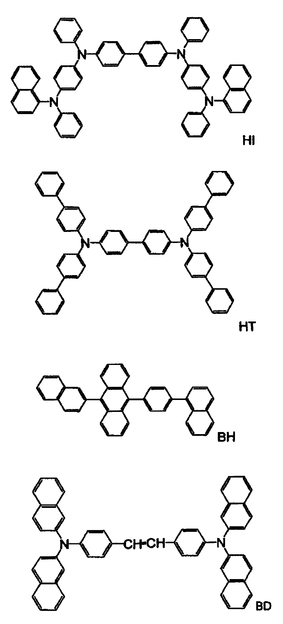
호스트 재료로서는 하기 화학식 1로 표시되는 재료를 이용하는 것이 바람직하다. It is preferable to use the material represented by following formula (1) as a host material.
![]()
![]()
식 중, Ar1은 핵 탄소수 6 내지 50의 방향족환, X는 치환기, l은 1 내지 5의 정수, m은 0 내지 6의 정수이다.In formula, Ar <1> is an aromatic ring of 6-50 carbon atoms, X is a substituent, l is an integer of 1-5, m is an integer of 0-6.
Ar1는 구체적으로는, 페닐환, 나프틸환, 안트라센환, 비페닐렌환, 아줄렌환, 아세나프틸렌환, 플루오렌환, 페난트렌환, 플루오란텐환, 아세페난트릴렌환, 트리페닐렌환, 피렌환, 크리센환, 나프타센환, 피센환, 페릴렌환, 펜타펜환, 펜타센환, 테트라페닐렌환, 헥사펜환, 헥사센환, 루비센환, 코로넨환, 트리나프틸렌환 등을 들 수 있다. Ar 1 is specifically a phenyl ring, naphthyl ring, anthracene ring, biphenylene ring, azulene ring, acenaphthylene ring, fluorene ring, phenanthrene ring, fluoranthene ring, acefenanthryl ring, triphenylene ring, pyrene Ring, chrysene ring, naphthacene ring, pisene ring, perylene ring, pentaphene ring, pentacene ring, tetraphenylene ring, hexaphene ring, hexacene ring, rubisen ring, coronene ring, trinaphthylene ring and the like.
X는 구체적으로는, 치환 또는 비치환된 핵 탄소수 6 내지 50의 방향족기, 치환 또는 비치환된 핵 원자수 5 내지 50의 방향족 복소환기, 치환 또는 비치환된 탄소수 1 내지 50의 알킬기, 치환 또는 비치환된 탄소수 1 내지 50의 알콕시기, 치환 또는 비치환된 탄소수 1 내지 50의 아르알킬기, 치환 또는 비치환된 핵 원자수 5 내지 50의 아릴옥시기, 치환 또는 비치환된 핵 원자수 5 내지 50의 아릴티오기, 치환 또는 비치환된 탄소수 1 내지 50의 카르복실기, 치환 또는 비치환된 스티릴기, 할로겐기, 시아노기, 니트로기, 히드록실기 등이다. X specifically represents a substituted or unsubstituted aromatic group having 6 to 50 carbon atoms, a substituted or unsubstituted aromatic heterocyclic group having 5 to 50 carbon atoms, a substituted or unsubstituted alkyl group having 1 to 50 carbon atoms, substituted or Unsubstituted alkoxy group having 1 to 50 carbon atoms, substituted or unsubstituted aralkyl group having 1 to 50 carbon atoms, substituted or unsubstituted aryloxy group having 5 to 50 atomic atoms, substituted or unsubstituted nuclear atom having 5 to 50 atoms A arylthio group of 50, a substituted or unsubstituted carboxyl group having 1 to 50 carbon atoms, a substituted or unsubstituted styryl group, a halogen group, a cyano group, a nitro group, a hydroxyl group and the like.
한편, 1≥2일 때, 1개의 Ar1은 각각 동일하거나 상이할 수 있다.On the other hand, when 1 ≧ 2, one Ar 1 may be the same or different, respectively.
또한 m≥2일 때, m개의 X는 각각 동일하거나 상이할 수 있다.In addition, when m ≧ 2, m Xs may be the same or different, respectively.
도펀트로서는 화학식 2로 표시되는 재료를 이용하는 것이 바람직하다.It is preferable to use the material represented by General formula (2) as a dopant.

식 중, Ar2 내지 Ar4는 치환 또는 비치환된 핵 탄소수 6 내지 50의 방향족기, 치환 또는 비치환된 스티릴기, p는 1 내지 4의 정수이다.In the formula, Ar 2 to Ar 4 are a substituted or unsubstituted aromatic group having 6 to 50 carbon atoms, a substituted or unsubstituted styryl group, and p is an integer of 1 to 4.
치환 또는 비치환된 핵 탄소수 6 내지 50의 방향족기의 예로서는, 페닐기, 1-나프틸기, 2-나프틸기, 1-안트릴기, 2-안트릴기, 9-안트릴기, 1-페난트릴기, 2-페난트릴기, 3-페난트릴기, 4-페난트릴기, 9-페난트릴기, 1-나프타세닐기, 2-나프타세닐기, 9-나프타세닐기, 1-피레닐기, 2-피레닐기, 4-피레닐기, 2-비페닐일기, 3-비페닐일기, 4-비페닐일기, p-터페닐-4-일기, p-터페닐-3-일기, p-터페닐-2-일기, m-터페닐-4-일기, m-터페닐-3-일기, m-터페닐-2-일기, o-톨릴기, m-톨릴기, p-톨릴기, p-t-부틸페닐기, p-(2-페닐프로필)페닐기, 3-메틸-2-나프틸기, 4-메틸-1-나프틸기, 4-메틸-1-안트릴기, 4'-메틸비페닐일기, 4''-t-부틸-p-터페닐-4-일기, 2-플루오레닐기, 9,9-디메틸-2-플루오레닐기, 3-플루오란테닐기 등을 들 수 있다. Examples of the substituted or unsubstituted aromatic group having 6 to 50 carbon atoms include a phenyl group, 1-naphthyl group, 2-naphthyl group, 1-anthryl group, 2-anthryl group, 9-anthryl group, 1-phenanthryl Group, 2-phenanthryl group, 3-phenanthryl group, 4-phenanthryl group, 9-phenanthryl group, 1-naphthasenyl group, 2-naphthacenyl group, 9-naphthacenyl group, 1-pyrenyl group, 2 -Pyrenyl group, 4-pyrenyl group, 2-biphenylyl group, 3-biphenylyl group, 4-biphenylyl group, p-terphenyl-4-yl group, p-terphenyl-3-yl group, p-terphenyl- 2-yl group, m-terphenyl-4-yl group, m-terphenyl-3-yl group, m-terphenyl-2-yl group, o-tolyl group, m-tolyl group, p-tolyl group, pt-butylphenyl group , p- (2-phenylpropyl) phenyl group, 3-methyl-2-naphthyl group, 4-methyl-1-naphthyl group, 4-methyl-1-anthryl group, 4'-methylbiphenylyl group, 4 '' -t-butyl-p-terphenyl-4-yl group, 2-fluorenyl group, 9,9-dimethyl-2-fluorenyl group, 3-fluoranthenyl group, etc. are mentioned.
치환 또는 비치환된 스티릴기의 예로서는 2-페닐-1-비닐기, 2,2-디페닐-1-비닐기, 1,2,2-트리페닐-1-비닐기 등을 들 수 있다. Examples of the substituted or unsubstituted styryl group include 2-phenyl-1-vinyl group, 2,2-diphenyl-1-vinyl group, 1,2,2-triphenyl-1-vinyl group and the like.
p는 1 내지 4의 정수이다. p is an integer from 1 to 4.
한편, p≥2일 때, p개의 Ar3, Ar4는 각각 동일하거나 상이할 수 있다. On the other hand, when p ≧ 2, p Ar 3 and Ar 4 may be the same or different, respectively.
다음으로, 정공 수송층은 반드시 필요한 것은 아니지만, 발광 성능의 향상을 위해 이용하는 편이 바람직하다. 이 정공 수송층으로서는 보다 낮은 전계로 정공을 유기 발광 매체에 수송하는 재료가 바람직하고, 또한 정공의 이동도가, 예를 들면 104 내지 106 V/cm의 전계 인가시에 적어도 10-6 ㎠/V·초이면 더욱 바람직하다. 정공 수송 재료는 상기의 바람직한 성질을 갖는 것이면 특별히 제한은 없고, 종래의 광 도전 재료에 있어서의 정공의 전하 수송재로서 관용되고 있는 것이나 EL 소자의 정공 수송층에 사용되는 공지된 것 중에서 임의의 것을 선택하여 사용할 수 있다. Next, the hole transport layer is not necessarily required, but it is preferable to use the hole transport layer for improving the light emission performance. As the hole transporting layer, a material for transporting holes to the organic light emitting medium with a lower electric field is preferable, and the mobility of holes is, for example, at least 10 −6
정공 수송층은 정공 수송 재료를, 예를 들면 진공 증착법, 스핀 코팅법, LB법 등의 공지된 박막법에 의해 제막하여 형성할 수 있다. The hole transport layer can be formed by forming a hole transport material into a film by a known thin film method such as vacuum deposition, spin coating, or LB.
이 정공 수송층의 막 두께는 특별히 제한은 없지만, 통상적으로는 5 ㎚ 내지 5 ㎛이다. 이 정공 수송층은 정공 수송 재료의 1종 또는 2종 이상으로 이루어지는 1층으로 구성될 수 있고, 또는 별종의 재료로 이루어지는 복수의 정공 수송층을 적층한 것일 수도 있다.Although the film thickness of this hole transport layer does not have a restriction | limiting in particular, Usually, it is 5 nm-5 micrometers. The hole transport layer may be composed of one or two layers of hole transport materials, or may be a laminate of a plurality of hole transport layers made of different materials.
전자를 유기 발광 매체 내에 머무르게 하기 위해 유기 발광 매체와 양극 사이에는 전자 장벽층을 사용할 수 있다. An electron barrier layer can be used between the organic light emitting medium and the anode to keep the electrons in the organic light emitting medium.
또한, 정공을 유기 발광 매체 내에 머무르게 하기 위해 유기 발광 매체와 음극 사이에는 정공 장벽층을 사용할 수 있다. In addition, a hole barrier layer may be used between the organic light emitting medium and the cathode to keep the holes in the organic light emitting medium.
전자 주입층은 전자 주입 재료로 이루어지는 것이며, 음극으로부터 주입된 전자를 유기 발광 매체에 전달하는 기능을 갖고 있다. 이러한 전자 주입 재료에 대하여 특별히 제한은 없고, 종래 공지된 화합물 중에서 임의의 것을 선택하여 사용할 수 있다. The electron injection layer is made of an electron injection material and has a function of transferring electrons injected from the cathode to the organic light emitting medium. There is no restriction | limiting in particular about such an electron injection material, Arbitrary thing can be selected and used out of a conventionally well-known compound.
전자 주입층은 전자 주입 재료를, 예를 들면 진공 증착법, 스핀 코팅법, 캐스팅법, LB법 등의 공지된 박막화법에 의해 제막하여 형성할 수 있다. The electron injection layer can be formed by forming an electron injection material into a film by a known thinning method such as vacuum deposition, spin coating, casting, or LB.
전자 주입층으로서의 막 두께는 통상적으로는 5 ㎚ 내지 5 ㎛의 범위에서 선택된다. 이 전자 주입층은 이들 전자 주입 재료의 1종 또는 2종 이상으로 이루어지는 1층으로 구성될 수 있고, 또는 다른 종류의 재료로 이루어지는 복수의 전자 주입층을 적층한 것일 수도 있다.The film thickness as an electron injection layer is normally selected in the range of 5 nm-5 micrometers. This electron injection layer may be comprised by the 1 layer which consists of 1 type, or 2 or more types of these electron injection materials, or may laminate | stack the some electron injection layer which consists of another kind of material.
또한, 부착 개선층으로서는 전자 전달성이 우수하면서, 유기 발광 매체 및 음극에 대하여 부착성이 높은 재료를 함유하는 것이 바람직하다. 이러한 재료로서는, 예를 들면 8-히드록시퀴놀린 또는 그의 유도체의 금속 착체, 예를 들면 옥신(일반적으로 8-퀴놀리놀 또는 8-히드록시퀴놀린)의 킬레이트를 포함하는 금속 킬레이트 옥시노이드 화합물을 들 수 있다. 구체적으로는, 트리스(8-퀴놀리놀)알루미늄, 트리스(5,7-디클로로-8-퀴놀리놀)알루미늄, 트리스(5,7-디브로모-8-퀴놀리놀)알루미늄, 트리스(2-메틸-8-퀴놀리놀)알루미늄, 및 알루미늄 이외의 인듐, 마그네슘, 구리, 갈륨, 주석, 납의 착체 등을 들 수 있다. Moreover, it is preferable that an adhesion improving layer contains the material which is excellent in electron transport property and high adhesiveness with respect to an organic light emitting medium and a cathode. As such a material, for example, a metal chelate oxynoid compound comprising a chelate of 8-hydroxyquinoline or a derivative thereof, for example a chelate of auxin (generally 8-quinolinol or 8-hydroxyquinoline) Can be. Specifically, tris (8-quinolinol) aluminum, tris (5,7-dichloro-8-quinolinol) aluminum, tris (5,7-dibromo-8-quinolinol) aluminum, tris ( And complexes of indium, magnesium, copper, gallium, tin, and lead other than 2-methyl-8-quinolinol) aluminum and aluminum.
5. 형광 변환부5. Fluorescence conversion unit
형광 변환부는 유기층으로부터 방출되는 중심 파장 λ의 빛의 색을 바꾸기 위해, 방출광을 취출하는 쪽가질되지 않고 내구성이 우수하기 때문에 바람직하다. 또한, 후술하는 반도체 밴드 갭을 이용하여 가시광을 흡수, 발광하는 미립자는 발광의 효율이 더욱 높아 바람직하다.In order to change the color of the light of the central wavelength λ emitted from the organic layer, the fluorescence conversion unit is preferable because it does not tend to extract the emitted light and is excellent in durability. Moreover, the microparticles | fine-particles which absorb and emit visible light using the semiconductor band gap mentioned later are preferable because the efficiency of light emission is further high.
형광 변환부는 형광체 미립자와 매트릭스 수지를 혼합하여 형성할 수 있다. The fluorescence conversion unit may be formed by mixing the phosphor fine particles and the matrix resin.
형광체 미립자로서는, 예를 들면 이하에 나타내는 무기 형광체 미립자 및 유기 형광체 미립자를 사용할 수 있다. As the phosphor fine particles, the inorganic phosphor fine particles and the organic phosphor fine particles shown below can be used, for example.
무기 형광체 미립자로는, 금속 화합물 등의 무기 화합물로 이루어지고, 가시광을 흡수하고, 흡수한 빛보다 긴 형광을 발하는 미립자를 사용할 수 있다. 미립자 표면에는 후술하는 매트릭스 수지에 대한 분산성 향상을 위해, 예를 들면, 장쇄 알킬기나 인산 등의 유기물로 표면을 개질할 수도 있다.As the inorganic phosphor fine particles, fine particles made of inorganic compounds such as metal compounds, which absorb visible light and emit fluorescence longer than the absorbed light can be used. In order to improve the dispersibility with respect to the matrix resin mentioned later, the surface of microparticles | fine-particles can also modify surface with organic substance, such as a long-chain alkyl group and phosphoric acid.
구체적으로는 이하의 미립자를 사용할 수 있다. Specifically, the following fine particles can be used.
(a) 금속 산화물에 전이 금속 이온을 도핑한 미립자 (a) Fine particles doped with transition metal ions in a metal oxide
Y2O3, Gd2O3, ZnO, Y3Al5O12, Zn2SiO4 등의 금속 산화물에, Eu2 +, Eu3 +, Ce3 +, Tb3 + 등의, 가시광을 흡수하는 전이 금속 이온을 도핑한 것. Y 2 O 3, Gd 2 O 3, ZnO,
(b) 금속 칼코게나이드물에 전이 금속 이온을 도핑한 미립자(b) fine particles doped with transition metal ions in a metal chalcogenide
ZnS, CdS, CdSe 등의 금속 칼코게나이드화물에 Eu2 +, Eu3 +, Ce3 +, Tb3 + 등의 가시광을 흡수하는 전이 금속 이온을 도핑한 것. S나 Se 등이, 후술하는 매트릭스 수지의 반응 성분에 의해 방출되는 것을 방지하기 위해, 실리카 등의 금속 산화물이나 유기물 등으로 표면 개질할 수도 있다.Eu 2 + to a metal chalcogenide such as a cargo ZnS, CdS, CdSe, Eu 3 +,
(c) 반도체의 밴드 갭을 이용하여 가시광을 흡수, 발광하는 미립자(c) Fine particles which absorb and emit visible light by using the band gap of the semiconductor
CdS, CdSe, CdTe, ZnS, ZnSe, InP 등의 반도체 미립자. 이들은 일본 특허 공표 제2002-510866호 공보 등의 문헌에서 알려져 있는 바와 같이, 입경을 나노 크기화함으로써 밴드 갭을 제어하고, 그 결과, 흡수-형광 파장을 바꿀 수 있다. S나 Se 등이, 후술하는 매트릭스 수지의 반응 성분에 의해 방출되는 것을 방지하기 위해, 실리카 등의 금속 산화물이나 유기물 등으로 표면 개질할 수도 있다.Semiconductor fine particles, such as CdS, CdSe, CdTe, ZnS, ZnSe, InP. These are known in the literature such as Japanese Patent Laid-Open No. 2002-510866, and the like, and control the band gap by nano-sizing the particle diameter, and as a result, the absorption-fluorescence wavelength can be changed. In order to prevent S, Se, etc. from being emitted by the reaction component of the matrix resin mentioned later, you may surface-modify with metal oxides, such as silica, organic substance, etc.
예를 들면, CdSe 미립자의 표면을 ZnS와 같은 보다 밴드 갭 에너지가 높은 반도체 재료의 쉘로 피복할 수 있다. 이에 따라 중심 미립자 내에 발생하는 전자의 구속 효과를 발현하기 쉬워진다.For example, the surface of the CdSe fine particles can be coated with a shell of a semiconductor material having a higher band gap energy such as ZnS. Thereby, it becomes easy to express the restraining effect of the electron which generate | occur | produces in a central fine particle.
한편, 상기 미립자는 1종 단독으로 사용할 수도 있고, 또한, 2종 이상을 조합하여 사용할 수도 있다. In addition, the said microparticles | fine-particles may be used individually by 1 type, and may be used in combination of 2 or more type.
유기 형광체 미립자로서는, 예를 들면 시아노기를 함유하는 J 회합성을 갖는 유기 형광 색소의 나노 결정 미립자를 들 수 있다. As organic fluorescent microparticles | fine-particles, the nanocrystal microparticles | fine-particles of the organic fluorescent dye which has J association property containing a cyano group are mentioned, for example.
매트릭스 수지는 형광체 미립자를 분산하는 수지이고, 비경화형 수지, 열 경화형 수지 또는 광 경화형 수지를 사용할 수 있다. 구체적으로는, 올리고머 또는 중합체 형태의 멜라민 수지, 페놀 수지, 알키드 수지, 에폭시 수지, 폴리우레탄 수지, 말레산 수지, 폴리아미드계 수지, 또는 폴리메틸메타크릴레이트, 폴리아크릴레이트, 폴리카보네이트, 폴리비닐알코올, 폴리비닐피롤리돈, 히드록시에틸셀룰로오스, 카르복시메틸셀룰로오스 등 및 이들을 형성하는 단량체를 구성 성분으로 하는 공중합체를 들 수 있다. Matrix resin is resin which disperse | distributes fluorescent substance microparticles | fine-particles, Uncurable resin, thermosetting resin, or photocurable resin can be used. Specifically, melamine resins, phenol resins, alkyd resins, epoxy resins, polyurethane resins, maleic acid resins, polyamide-based resins, or polymethyl methacrylates, polyacrylates, polycarbonates, polyvinyls in the form of oligomers or polymers Alcohols, polyvinylpyrrolidone, hydroxyethyl cellulose, carboxymethyl cellulose, and the like and copolymers containing the monomers forming them as constituents.
형광 변환부의 패턴화 목적으로 광 경화형 수지를 사용할 수 있다. 광 경화형 수지로서는 통상적으로 감광제를 포함하는 반응성 비닐기를 갖는 아크릴산, 메타크릴산계의 광 중합형이나, 폴리신남산비닐 등의 광 가교형 등이 이용된다. 한편, 감광제를 포함하지 않는 경우에는 열 경화형의 것을 이용할 수도 있다.Photocurable resin can be used for the purpose of patterning a fluorescent conversion part. As photocurable resin, the photopolymerization type of acrylic acid, methacrylic acid system which have a reactive vinyl group containing a photosensitizer, the photocrosslinking type, such as polyvinyl cinnamate, etc. are used normally. On the other hand, when it does not contain a photosensitizer, a thermosetting type can also be used.
한편, 풀 컬러 디스플레이에서는 서로 분리한 형광체층을 매트릭스형으로 배치한 형광 변환부를 형성한다. 이 때문에, 매트릭스 수지로서는 포토리소그래피법을 적용할 수 있는 광 경화형 수지를 사용하는 것이 바람직하다. On the other hand, in a full color display, a fluorescent conversion unit in which phosphor layers separated from each other are arranged in a matrix form is formed. For this reason, it is preferable to use photocurable resin which can apply the photolithographic method as matrix resin.
또한, 이들 매트릭스 수지는 1종의 수지를 단독으로 이용할 수 있고, 복수 종류를 혼합하여 이용할 수도 있다.In addition, these matrix resins can be used individually by 1 type, and can also mix and use multiple types.
형광 변환부의 제조는 형광체 미립자와 매트릭스 수지를 밀링법이나 초음파 분산법 등의 공지된 방법을 이용하여 혼합·분산된 분산액을 사용함으로써 행한다. 이 때, 매트릭스 수지에 있어서의 양용매를 사용할 수 있다. 이 형광체 미립자 분산액을 공지된 성막 방법, 예를 들면, 스핀 코팅법, 스크린 인쇄법 등에 의해 지지 기판 상에 성막하여 형광 변환부를 제조한다. The fluorescence conversion unit is produced by using a dispersion liquid in which the phosphor fine particles and the matrix resin are mixed and dispersed using a known method such as a milling method or an ultrasonic dispersion method. At this time, the good solvent in matrix resin can be used. This phosphor fine particle dispersion is formed on a support substrate by a well-known film formation method, for example, a spin coating method, a screen printing method, or the like to produce a fluorescence conversion portion.
그 밖에, 공지된 쿠마린류, 로다민류, 플루오레세인류, 시아닌류, 포르피린류, 나프탈이미드류, 페릴렌류, 퀴나크리돈류 등의 유기 형광체를 중합체 중에 분산하여 사용할 수 있다. 중합체 결합제로서는 투명성 수지, 예를 들면 폴리메타크릴레이트, 폴리카보네이트, 폴리염화비닐, 폴리이미드, 폴리아미드산, 폴리올레핀, 폴리스티렌 등을 사용할 수 있다. In addition, organic phosphors such as known coumarins, rhodamines, fluoresceins, cyanines, porphyrins, naphthalimides, perylenes and quinacridones can be dispersed and used in a polymer. As the polymer binder, a transparent resin such as polymethacrylate, polycarbonate, polyvinyl chloride, polyimide, polyamic acid, polyolefin, polystyrene and the like can be used.
6. 컬러 필터6. Color filter
또한, 필요에 따라 색 순도를 조정하기 위한 컬러 필터를 사용할 수 있다. 컬러 필터 재료로서는 색소 또는 색소를 결합제 수지 중에 용해 또는 분산시킨 고체 상태의 것을 들 수 있다. 색소의 예로서는, 구리 프탈로시아닌계 안료, 인단트론계 안료, 인도페놀계 안료, 시아닌계 안료, 디옥사진계 안료 등을 들 수 있고, 1종 단독, 또는 2종 이상의 혼합물로 이용할 수 있다. 색소의 결합제 수지의 예로서는, 폴리메틸메타크릴레이트, 폴리아크릴레이트, 폴리카보네이트, 폴리비닐알코올, 폴리비닐피롤리돈, 히드록시에틸셀룰로오스, 카르복시메틸셀룰로오스 등의 투명 수지(고분자) 등을 들 수 있고, 1종 단독 또는 2종 이상을 혼합하여 이용할 수 있다. 한편, 결합제 수지는 포토리소그래피법을 적용할 수 있는 감광성 수지를 사용하는 것이 바람직하다. 이러한 감광성 수지의 예로서는, 아크릴산계, 메타크릴산계, 폴리신남산비닐계, 환화 고무계 등의 반응성 비닐기를 갖는 광 경화형 레지스트 재료 등을 들 수 있다. 이들 감광성 수지는 1종 단독으로 또는 2종 이상을 혼합하여 사용할 수 있다. In addition, a color filter for adjusting the color purity can be used as necessary. As a color filter material, the solid state which melt | dissolved or disperse | distributed the pigment | dye or pigment | dye in binder resin is mentioned. Examples of the pigment include copper phthalocyanine pigments, indanthrone pigments, indophenol pigments, cyanine pigments, dioxazine pigments, and the like, and can be used alone or in a mixture of two or more thereof. Examples of the binder resin of the dye include transparent resins (polymers) such as polymethyl methacrylate, polyacrylate, polycarbonate, polyvinyl alcohol, polyvinylpyrrolidone, hydroxyethyl cellulose and carboxymethyl cellulose. , 1 type can be used individually or in mixture of 2 or more types. On the other hand, it is preferable to use photosensitive resin to which binder resin can apply the photolithographic method. As an example of such photosensitive resin, the photocurable resist material etc. which have reactive vinyl groups, such as acrylic acid type, methacrylic acid type, polyvinyl cinnamic acid type, and cyclization rubber type, are mentioned. These photosensitive resins can be used individually by 1 type or in mixture of 2 or more types.
실시예Example 1 One
(1) 색 변환 기판의 제조(1) Manufacture of color conversion substrate
두께 0.7 ㎜의 유리판에 안료계 적색 컬러 필터 재료(CRY-S840B, 후지필름 아크사 제조)를 스핀 코팅하고, 자외선 노광한 후, 200 ℃에서 소성하여 적색 컬러 필터(막 두께 1.2 ㎛) 기판을 얻었다. A pigment-based red color filter material (CRY-S840B, manufactured by FUJIFILM ARC Co., Ltd.) was spin-coated on a glass plate having a thickness of 0.7 mm, exposed to ultraviolet light, and then fired at 200 ° C to obtain a red color filter (film thickness 1.2 m) substrate. .
매트릭스 수지로서 메타크릴산-메타크릴산메틸 공중합체(메타크릴산 공중합 비=15 내지 20%, Mw=20,000 내지 25,000)를 이용하고, 이것을 1-메톡시-2-아세톡시프로판에 용해시키고, 입경 5.1 ㎚의 CdSe 미립자(형광 파장 606 ㎚)를 첨가하였다. 첨가 비율은 전체 고형 농도에 대한 CdSe 입자의 중량 비율이 17.8 중량%로 하였다.Methacrylic acid-methyl methacrylate copolymer (methacrylic acid copolymerization ratio = 15-20%, Mw = 20,000-25,000) was used as a matrix resin, this was dissolved in 1-methoxy-2-acetoxy propane, CdSe fine particles (fluorescence wavelength 606 nm) having a particle diameter of 5.1 nm were added. The addition ratio was made into 17.8 weight% the weight ratio of CdSe particle with respect to total solid concentration.
이것을 앞서 제조한 적색 컬러 필터 기판의 컬러 필터막 상에 스핀 코팅하고, 200 ℃에서 30분의 건조 처리를 행하여 적색 컬러 필터와 색 변환막을 적층한 색 변환 기판을 얻었다. 색 변환막의 400 내지 500 ㎚의 여기 스펙트럼에 있어서의 최대 파장은 400 ㎚이고, 막 두께는 17 ㎛였다. This was spin-coated on the color filter film of the red color filter board | substrate previously manufactured, and the drying process was performed for 30 minutes at 200 degreeC, and the color conversion board | substrate which laminated | stacked the red color filter and the color conversion film was obtained. The maximum wavelength in the 400-500 nm excitation spectrum of the color conversion film was 400 nm, and the film thickness was 17 μm.
(2) 유기 EL 소자의 제조(2) Fabrication of Organic EL Device
두께 1.1 ㎜의 유리 기판(코닝 7059)을 이소프로필알코올 중에서 초음파세정을 5분간 행한 후, UV 오존 세정을 30분간 행하였다. 세정 후의 유리 기판을 진공 증착 장치의 기판 홀더에 장착하였다. After a 1.1-mm-thick glass substrate (Corning 7059) was ultrasonically cleaned for 5 minutes in isopropyl alcohol, UV ozone cleaning was performed for 30 minutes. The glass substrate after washing | cleaning was attached to the substrate holder of a vacuum vapor deposition apparatus.
이 유리 기판 상에 스퍼터링에 의해 막 두께 300 ㎚의 알루미늄을 성막하였다. 이 알루미늄막은 양극으로서 기능하는 동시에 제1 광 반사 부재로서 기능한다. 이 알루미늄막 상에 스퍼터링에 의해 막 두께 10 ㎚의 ITO를 성막하였다. 이 ITO 막은 정공 주입 전극(양극)으로서 기능한다. The aluminum with a film thickness of 300 nm was formed into a film by sputtering on this glass substrate. This aluminum film functions as an anode and as a first light reflecting member. ITO with a film thickness of 10 nm was formed into a film by sputtering on this aluminum film. This ITO film functions as a hole injection electrode (anode).
다음으로, 이 ITO막 상에 하기 화합물 HI로 이루어지는 막을 20 ㎚의 막 두께가 되도록 성막하였다. 이 HI막은 정공 주입층으로서 기능한다. 이 HI막 상에 하기 화합물 HT로 이루어지는 막을 15 ㎚의 막 두께가 되도록 성막하였다. 이 HT막은 정공 수송층으로서 기능한다. Next, the film which consists of following compound HI on this ITO film | membrane was formed into a film thickness of 20 nm. This HI film functions as a hole injection layer. On this HI film, a film made of the following compound HT was formed so as to have a film thickness of 15 nm. This HT film functions as a hole transport layer.
또한, 이 HT막 상에 막 두께 30 ㎚으로, 하기 화합물 BH를 호스트 재료로 하고, 하기 화합물 BD를 도펀트 재료로 하여 30:1.8의 비가 되도록 공증착하여 성막하고, 발광층(청색계 발광층)으로 하였다.Further, the film was co-deposited on the HT film at a thickness of 30 nm with the following compound BH as a host material and the following compound BD as a dopant material to form a light emitting layer (blue light emitting layer). .
이 막 상에 트리스(8-퀴놀리놀)알루미늄(Alq)막을 10 ㎚의 막 두께가 되도록 성막하였다. 이 Alq막은 전자 수송층으로서 기능한다. 이 Alq막 상에 LiF를 막 두께 1 ㎚으로 증착시켜 전자 주입 음극을 형성하였다. 또한 마그네슘과 은이 9:1이 되는 바와 같은 합금막을 10 ㎚의 막 두께가 되도록 성막하였다. 이 Mg:Ag막은 금속 음극으로서 기능하는 동시에 제2 광 반사 부재로서 기능한다. 또한, 상부 투명 전극(음극)으로서, IZO를 75 ㎚의 막 두께로 스퍼터링 성막하였다. 마지막으로, 유기 EL 발광부 전체를 덮도록, 밀봉층으로서, 유기 EL 소자의 상부 전극 상에 투명 무기막인 SiOxNy(O/(O+N)=50%: Atomic Ratio)를 저온 CVD에 의해 1000 ㎚의 두께로 성막하여 유기 EL 소자를 제조하였다. On this film, a tris (8-quinolinol) aluminum (Alq) film was formed to have a film thickness of 10 nm. This Alq film functions as an electron transport layer. LiF was deposited on the Alq film with a film thickness of 1 nm to form an electron injection cathode. Further, an alloy film in which magnesium and silver were 9: 1 was formed to have a film thickness of 10 nm. This Mg: Ag film functions as a metal cathode and as a second light reflecting member. In addition, IZO was sputtered into a film at a film thickness of 75 nm as the upper transparent electrode (cathode). Finally, as a sealing layer, SiO x N y (O / (O + N) = 50%: Atomic Ratio), which is a transparent inorganic film, was formed on the upper electrode of the organic EL device by low temperature CVD so as to cover the entire organic EL light emitting part. It formed into a film at thickness of 1000 nm, and manufactured organic electroluminescent element.
(3) 유기 EL 표시 장치의 제조(3) Fabrication of Organic EL Display Device
상기 (1)에서 얻어진 색 변환 기판을 상기 (2)에서 제조한 유기 EL 소자 상에 유기 EL 소자의 발광면(밀봉층측)과 색 변환 기판의 막면이 대향하도록 배치하였다. 또한, 색 변환 기판의 주변부에 대하여 양이온 경화형 접착제 TB3102(쓰리 본드(주) 제조)로 처리하고, 광 경화시켜 유기 EL 표시 장치를 제조하였다. The color conversion board | substrate obtained by said (1) was arrange | positioned so that the light emitting surface (sealing layer side) of the organic electroluminescent element and the film surface of a color conversion substrate may face on the organic electroluminescent element manufactured by said (2). In addition, the peripheral part of the color conversion substrate was treated with a cationic curable adhesive TB3102 (manufactured by Three Bond Co., Ltd.) and photocured to manufacture an organic EL display device.
(4) 유기 EL 표시 장치의 평가(4) Evaluation of Organic EL Display Device
얻어진 유기 EL 소자에 6.8 V를 인가하고, 분광 방사 휘도계(CS1000: 미놀타 제조)로 발광 특성을 조사한 결과, 청색 발광 피크 파장은 469 ㎚, 휘도(L) 999 nit, 색도(CIE)(0.134,0.219)였다. 6.8 V was applied to the obtained organic EL device, and the light emission characteristics were examined with a spectroradiometer (CS1000: manufactured by Minolta). As a result, the blue light emission peak wavelength was 469 nm, luminance (L) 999 nit, and chromaticity (CIE) (0.134, 0.219).
색 변환 기판을 접합시킨 후의 발광 특성(6.8 V 인가)은 휘도 변환 효율(η) 63%, 휘도 625 nit, 색도(0.633,0.364)의 양호한 적색임을 확인하였다. It was confirmed that the light emission characteristics (applied with 6.8 V) after bonding the color conversion substrate were good red of 63% of luminance conversion efficiency (η), 625 nit of luminance, and chromaticity (0.633, 0.364).
여기서, 휘도 변환 효율(η)은 이하의 식으로 구하였다.Here, the luminance conversion efficiency η was obtained by the following equation.
η=[(유기 EL 소자만의 휘도 nit)/(유기 EL 소자에 색 변환 기판을 접합시켰을 때의 휘도 nit)]×100η = [(luminance nit only for organic EL elements) / (luminance nit when a color conversion substrate is bonded to the organic EL element)] × 100
또한, 얻어진 유기 EL 소자의 적색 발광 휘도가 1000 nit가 되도록 전류치를 조절하고, 실온에서 정전류 연속 구동 시험을 행한 결과, 휘도가 40% 감소했을 때의 시간(수명)(t60%)은 8860 시간이었다.Furthermore, when the current value was adjusted so that the red light emission luminance of the obtained organic EL element might be 1000 nit, and a constant current continuous drive test was conducted at room temperature, the time (life time) (t60%) when the luminance decreased by 40% was 8860 hours. .
결과를 표 1에 나타내었다.The results are shown in Table 1.
비교예Comparative example 1 One
(1) 색 변환 기판의 제조(1) Manufacture of color conversion substrate
실시예 1(1)과 동일하게 하여 색 변환 기판을 제조하였다.A color conversion substrate was manufactured in the same manner as in Example 1 (1).
(2) 유기 EL 소자의 제조(2) Fabrication of Organic EL Device
두께 1.1 ㎜의 유리 기판(코닝 7059)을 이소프로필알코올 중에서 초음파세정을 5분간 행한 후에 UV 오존 세정을 30분간 행하였다. 세정 후의 유리 기판을 진공 증착 장치의 기판 홀더에 장착하였다. A glass substrate (Corning 7059) having a thickness of 1.1 mm was subjected to ultrasonic cleaning in isopropyl alcohol for 5 minutes, followed by UV ozone cleaning for 30 minutes. The glass substrate after washing | cleaning was attached to the substrate holder of a vacuum vapor deposition apparatus.
이 유리 기판 상에 스퍼터링에 의해 막 두께 130 ㎚의 ITO를 성막하였다. 이 ITO 막은 정공 주입 전극(양극)으로서 기능한다. ITO with a film thickness of 130 nm was formed into a film by sputtering on this glass substrate. This ITO film functions as a hole injection electrode (anode).
다음으로, 이 ITO막 상에 하기 화합물 HI로 이루어지는 막을 60 ㎚의 막 두께가 되도록 성막하였다. 이 HI막은 정공 주입층으로서 기능한다. 이 HI막 상에 하기 화합물 HT로 이루어지는 막을 20 ㎚의 막 두께가 되도록 성막하였다. 이 HT막은 정공 수송층으로서 기능한다. Next, the film which consists of following compound HI on this ITO film | membrane was formed into a film thickness of 60 nm. This HI film functions as a hole injection layer. On this HI film, a film made of the following compound HT was formed so as to have a film thickness of 20 nm. This HT film functions as a hole transport layer.
또한, 이 HT막 상에 막 두께 40 ㎚로, 하기 화합물 BH를 호스트 재료로 하고 하기 화합물 BD를 도펀트 재료로 하여 40:2.0의 비가 되도록 공증착하여 성막하여 발광층(청색계 발광층)으로 하였다.On the HT film, the film was co-deposited at a thickness of 40 nm with the following compound BH as a host material and the following compound BD as a dopant material to form a light emitting layer (blue light emitting layer).
이 막 상에 트리스(8-퀴놀리놀)알루미늄(Alq)막을 20 ㎚의 막 두께가 되도록 성막하였다. 이 Alq막은 전자 수송층으로서 기능한다. 이 Alq막 상에 LiF를 막 두께 1 ㎚로 증착시켜 전자 주입 음극을 형성하였다. 추가로 그 위에 금속 음극으로서 Al막을 300 ㎚의 두께로 스퍼터링 성막하였다. 마지막으로, 유기 EL 발광부 전체를 덮도록, 밀봉층으로서, 유기 EL 소자의 상부 전극 상에 투명 무기막인 SiOxNy(O/(O+N)=50%: Atomic Ratio)를 저온 CVD에 의해 1000 ㎚의 두께로 성막하여 유기 EL 소자를 제조하였다. On this film, a tris (8-quinolinol) aluminum (Alq) film was formed to have a film thickness of 20 nm. This Alq film functions as an electron transport layer. LiF was deposited to a thickness of 1 nm on the Alq film to form an electron injection cathode. Furthermore, the Al film | membrane was sputtered into a film at 300 nm in thickness as a metal cathode on it. Finally, as a sealing layer, SiO x N y (O / (O + N) = 50%: Atomic Ratio), which is a transparent inorganic film, was formed on the upper electrode of the organic EL device by low temperature CVD so as to cover the entire organic EL light emitting part. It formed into a film at thickness of 1000 nm, and manufactured organic electroluminescent element.
(3) 유기 EL 표시 장치의 제조(3) Fabrication of Organic EL Display Device
상기 (1)에서 얻어진 색 변환 기판을 상기 (2)에서 제조한 유기 EL 소자 상에 유기 EL 소자의 발광면과 색 변환 기판의 막면이 대향하도록 배치하였다. 또한, 색 변환 기판의 주변부에 대하여 양이온 경화형 접착제 TB3102(쓰리 본드(주) 제조)로 처리하고, 광 경화시켜 유기 EL 표시 장치를 제조하였다. The color conversion board | substrate obtained by said (1) was arrange | positioned so that the light emitting surface of an organic electroluminescent element and the film surface of a color conversion substrate may face on the organic electroluminescent element manufactured by said (2). In addition, the peripheral part of the color conversion substrate was treated with a cationic curable adhesive TB3102 (manufactured by Three Bond Co., Ltd.) and photocured to manufacture an organic EL display device.
(4) 유기 EL 표시 장치의 평가(4) Evaluation of Organic EL Display Device
실시예 1과 동일하게 평가하였다. 결과를 표 1에 나타내었다. It evaluated similarly to Example 1. The results are shown in Table 1.
얻어진 유기 EL 소자 6.8 V 인가시에는 청색의 발광 피크 파장 472 ㎚, 휘도(L) 1205 nit, 색도(CIE)(0.167,0.325)였다. When the obtained organic EL device was applied with 6.8 V, the blue light emission peak wavelength was 472 nm, the luminance (L) 1205 nit, and the chromaticity (CIE) (0.167, 0.325).
색 변환 기판을 접합시킨 후의 발광 특성(6.8 V 인가)은 휘도 변환 효율(η) 46%, 휘도(L) 552 nit, 색도(CIE)(0.630,0.367)이고, 휘도 변환 효율은 실시예 1의 8할 이하이고, 휘도는 실시예 1의 9할 이하였다. The luminescence properties (6.8 V applied) after bonding the color conversion substrate were 46% luminance conversion efficiency (η), 552 nit luminance (L), and chromaticity (CIE) (0.630, 0.367). It was 80% or less, and the brightness | luminance was 90% or less of Example 1.
또한, 얻어진 유기 EL 소자의 적색 발광 휘도가 100O nit가 되도록 전류치를 조절하고, 실온에서 정전류 연속 구동 시험을 행한 결과, 휘도가 40% 감소했을 때의 시간(수명)(t60%)은 5547 시간이고, 실시예 1의 6할 정도였다.The current value was adjusted so that the red light emission luminance of the obtained organic EL device was 100Onit, and the constant current continuous drive test was performed at room temperature. As a result, the time (life time) (t60%) when the luminance was reduced by 40% was 5547 hours. It was about 60% of Example 1.

본 발명의 유기 EL 소자 및 표시 장치는 일반 TV, 대형 표시 디스플레이, 휴대 전화용 표시 화면 등의 각종 표시 장치에 사용할 수 있다. The organic EL element and display apparatus of this invention can be used for various display apparatuses, such as a general TV, a large display display, and the display screen for mobile phones.
Claims (10)
Applications Claiming Priority (2)
| Application Number | Priority Date | Filing Date | Title |
|---|---|---|---|
| JPJP-P-2004-00208091 | 2004-07-15 | ||
| JP2004208091 | 2004-07-15 |
Publications (1)
| Publication Number | Publication Date |
|---|---|
| KR20070044432A true KR20070044432A (en) | 2007-04-27 |
Family
ID=35785103
Family Applications (1)
| Application Number | Title | Priority Date | Filing Date |
|---|---|---|---|
| KR1020077000798A Withdrawn KR20070044432A (en) | 2004-07-15 | 2005-07-08 | Organic EL display |
Country Status (7)
| Country | Link |
|---|---|
| US (1) | US20060158103A1 (en) |
| EP (1) | EP1768467A4 (en) |
| JP (1) | JPWO2006008987A1 (en) |
| KR (1) | KR20070044432A (en) |
| CN (1) | CN1977568A (en) |
| TW (1) | TW200614864A (en) |
| WO (1) | WO2006008987A1 (en) |
Cited By (2)
| Publication number | Priority date | Publication date | Assignee | Title |
|---|---|---|---|---|
| KR20130048965A (en) * | 2011-11-03 | 2013-05-13 | 엘지디스플레이 주식회사 | Organic electroluminescent diode |
| KR20140040436A (en) * | 2012-09-26 | 2014-04-03 | 엘지디스플레이 주식회사 | Light emitting diode |
Families Citing this family (18)
| Publication number | Priority date | Publication date | Assignee | Title |
|---|---|---|---|---|
| JP4899418B2 (en) * | 2005-10-28 | 2012-03-21 | セイコーエプソン株式会社 | LIGHT EMITTING DEVICE AND ELECTRONIC DEVICE |
| WO2007096538A2 (en) * | 2006-02-27 | 2007-08-30 | Commissariat A L'energie Atomique | Organic light-emitting diode with a multilayer transparent electrode |
| JP2007299689A (en) * | 2006-05-02 | 2007-11-15 | Seiko Epson Corp | Organic electroluminescence device and electronic device |
| TWI308401B (en) | 2006-07-04 | 2009-04-01 | Epistar Corp | High efficient phosphor-converted light emitting diode |
| JP2008041361A (en) * | 2006-08-03 | 2008-02-21 | Idemitsu Kosan Co Ltd | Fluorescence conversion medium and color light emitting device including the same |
| US7969085B2 (en) * | 2006-08-18 | 2011-06-28 | Global Oled Technology Llc | Color-change material layer |
| WO2008149469A1 (en) * | 2007-06-07 | 2008-12-11 | Kazufumi Ogawa | Pattern-like fluor fine particle film and manufacturing method thereof |
| JP5008486B2 (en) * | 2007-07-19 | 2012-08-22 | キヤノン株式会社 | Display device |
| US8916890B2 (en) * | 2008-03-19 | 2014-12-23 | Cree, Inc. | Light emitting diodes with light filters |
| JP5211996B2 (en) * | 2008-09-30 | 2013-06-12 | 豊田合成株式会社 | Light emitting device |
| TWI396313B (en) * | 2009-04-29 | 2013-05-11 | Innolux Corp | Organic light-emitting element |
| WO2011145358A1 (en) * | 2010-05-21 | 2011-11-24 | シャープ株式会社 | Phosphor substrate, light-emitting element, and display device using same |
| US8957412B2 (en) | 2010-11-29 | 2015-02-17 | Panasonic Corporation | Organic electroluminescence panel, method of manufacturing organic electroluminescence panel, organic light emitting apparatus using organic electroluminescence panel, and organic display apparatus using organic electroluminescence panel |
| KR102113034B1 (en) * | 2013-05-29 | 2020-05-21 | 삼성디스플레이 주식회사 | Organic light emitting display device and manufacturing method thereof |
| JPWO2018123805A1 (en) * | 2016-12-28 | 2019-10-31 | Dic株式会社 | Light emitting device and image display device using the same |
| JP2018120733A (en) * | 2017-01-25 | 2018-08-02 | 株式会社ジャパンディスプレイ | Display device |
| CN107565053B (en) * | 2017-08-25 | 2019-09-24 | 上海天马有机发光显示技术有限公司 | Display panel and display device |
| WO2021038475A1 (en) * | 2019-08-27 | 2021-03-04 | Oti Lumionics Inc. | Light transmissive electrode for light emitting devices |
Family Cites Families (17)
| Publication number | Priority date | Publication date | Assignee | Title |
|---|---|---|---|---|
| US5405710A (en) * | 1993-11-22 | 1995-04-11 | At&T Corp. | Article comprising microcavity light sources |
| TW386609U (en) * | 1996-10-15 | 2000-04-01 | Koninkl Philips Electronics Nv | Electroluminescent illumination apparatus |
| US6501091B1 (en) * | 1998-04-01 | 2002-12-31 | Massachusetts Institute Of Technology | Quantum dot white and colored light emitting diodes |
| US6140764A (en) * | 1998-07-20 | 2000-10-31 | Motorola, Inc. | Organic electroluminescent apparatus with mircrocavity |
| US6656608B1 (en) * | 1998-12-25 | 2003-12-02 | Konica Corporation | Electroluminescent material, electroluminescent element and color conversion filter |
| JP2001210471A (en) * | 2000-01-27 | 2001-08-03 | Motorola Inc | Organic electroluminescence device |
| ATE344538T1 (en) * | 2000-02-09 | 2006-11-15 | Motorola Inc | ELECTROLUMINESCENT DEVICE AND METHOD OF PRODUCTION |
| EP1124274A1 (en) * | 2000-02-09 | 2001-08-16 | Motorola, Inc. | Organic electroluminescent apparatus |
| US6515314B1 (en) * | 2000-11-16 | 2003-02-04 | General Electric Company | Light-emitting device with organic layer doped with photoluminescent material |
| JP2002359076A (en) * | 2001-03-27 | 2002-12-13 | Konica Corp | Organic electroluminescence element, display device, light emitting method, display method, and transparent substrate |
| JP2005512303A (en) * | 2001-12-12 | 2005-04-28 | コーニンクレッカ フィリップス エレクトロニクス エヌ ヴィ | Electroluminescent device with improved contrast |
| JP2004014335A (en) * | 2002-06-07 | 2004-01-15 | Konica Minolta Holdings Inc | Organic electroluminescent (el) element, display device, light emitting method, and display method |
| US20060152150A1 (en) * | 2002-10-01 | 2006-07-13 | Herbert Boerner | Electroluminescent display with improved light outcoupling |
| JP3703028B2 (en) * | 2002-10-04 | 2005-10-05 | ソニー株式会社 | Display element and display device using the same |
| US20040140758A1 (en) * | 2003-01-17 | 2004-07-22 | Eastman Kodak Company | Organic light emitting device (OLED) display with improved light emission using a metallic anode |
| CN1543270A (en) * | 2003-02-20 | 2004-11-03 | ������������ʽ���� | Color light emitting display device |
| JP4716699B2 (en) * | 2003-09-30 | 2011-07-06 | 三洋電機株式会社 | Organic EL panel |
-
2005
- 2005-07-08 KR KR1020077000798A patent/KR20070044432A/en not_active Withdrawn
- 2005-07-08 EP EP05758316A patent/EP1768467A4/en not_active Withdrawn
- 2005-07-08 JP JP2006529003A patent/JPWO2006008987A1/en not_active Withdrawn
- 2005-07-08 WO PCT/JP2005/012666 patent/WO2006008987A1/en not_active Ceased
- 2005-07-08 CN CNA2005800220566A patent/CN1977568A/en active Pending
- 2005-07-13 TW TW094123770A patent/TW200614864A/en unknown
- 2005-12-05 US US11/293,127 patent/US20060158103A1/en not_active Abandoned
Cited By (3)
| Publication number | Priority date | Publication date | Assignee | Title |
|---|---|---|---|---|
| KR20130048965A (en) * | 2011-11-03 | 2013-05-13 | 엘지디스플레이 주식회사 | Organic electroluminescent diode |
| KR20140040436A (en) * | 2012-09-26 | 2014-04-03 | 엘지디스플레이 주식회사 | Light emitting diode |
| KR101948751B1 (en) * | 2012-09-26 | 2019-02-15 | 엘지디스플레이 주식회사 | Light emitting diode |
Also Published As
| Publication number | Publication date |
|---|---|
| US20060158103A1 (en) | 2006-07-20 |
| EP1768467A1 (en) | 2007-03-28 |
| CN1977568A (en) | 2007-06-06 |
| JPWO2006008987A1 (en) | 2008-05-01 |
| EP1768467A4 (en) | 2009-01-21 |
| TW200614864A (en) | 2006-05-01 |
| WO2006008987A1 (en) | 2006-01-26 |
Similar Documents
| Publication | Publication Date | Title |
|---|---|---|
| KR20070044432A (en) | Organic EL display | |
| US7928647B2 (en) | Composite emitting device | |
| JP3224237B2 (en) | Organic electroluminescence display device | |
| EP1737276A1 (en) | Organic el display and full color device | |
| WO2008015807A1 (en) | Fluorescence conversion medium and apparatus for color luminescence employing the same | |
| KR20070042153A (en) | Color light emitting device | |
| TW200803600A (en) | Light emitting device | |
| JPWO2005097939A1 (en) | Fluorescence conversion medium and color light emitting device | |
| WO2005086539A1 (en) | Organic electroluminescence display device | |
| CN100505967C (en) | Organic electroluminescent display device | |
| EP1956870B1 (en) | Organic el light emitting device | |
| US7221090B2 (en) | Blue organic electroluminescent device and display using same | |
| JP2846483B2 (en) | Organic electroluminescence device and method of manufacturing the same | |
| JP4692257B2 (en) | Color conversion film and multicolor organic EL device using the same | |
| KR20070017360A (en) | Organic electroluminescent display | |
| JP2002231452A (en) | Organic EL display device and manufacturing method thereof | |
| US10396305B2 (en) | Organic EL device, and display apparatus and lighting apparatus using the same | |
| KR20070017346A (en) | Organic EL display and full color device |
Legal Events
| Date | Code | Title | Description |
|---|---|---|---|
| PA0105 | International application |
Patent event date: 20070112 Patent event code: PA01051R01D Comment text: International Patent Application |
|
| PG1501 | Laying open of application | ||
| PC1203 | Withdrawal of no request for examination | ||
| WITN | Application deemed withdrawn, e.g. because no request for examination was filed or no examination fee was paid |