KR20060055437A - Switching element, driving method, rewritable logic integrated circuit and memory element - Google Patents
Switching element, driving method, rewritable logic integrated circuit and memory element Download PDFInfo
- Publication number
- KR20060055437A KR20060055437A KR1020057009746A KR20057009746A KR20060055437A KR 20060055437 A KR20060055437 A KR 20060055437A KR 1020057009746 A KR1020057009746 A KR 1020057009746A KR 20057009746 A KR20057009746 A KR 20057009746A KR 20060055437 A KR20060055437 A KR 20060055437A
- Authority
- KR
- South Korea
- Prior art keywords
- electrode
- switching element
- state
- ion conductor
- voltage
- Prior art date
- Legal status (The legal status is an assumption and is not a legal conclusion. Google has not performed a legal analysis and makes no representation as to the accuracy of the status listed.)
- Granted
Links
Images


Classifications
-
- H—ELECTRICITY
- H10—SEMICONDUCTOR DEVICES; ELECTRIC SOLID-STATE DEVICES NOT OTHERWISE PROVIDED FOR
- H10N—ELECTRIC SOLID-STATE DEVICES NOT OTHERWISE PROVIDED FOR
- H10N70/00—Solid-state devices having no potential barriers, and specially adapted for rectifying, amplifying, oscillating or switching
- H10N70/801—Constructional details of multistable switching devices
- H10N70/841—Electrodes
- H10N70/8416—Electrodes adapted for supplying ionic species
-
- G—PHYSICS
- G11—INFORMATION STORAGE
- G11C—STATIC STORES
- G11C13/00—Digital stores characterised by the use of storage elements not covered by groups G11C11/00, G11C23/00, or G11C25/00
- G11C13/0002—Digital stores characterised by the use of storage elements not covered by groups G11C11/00, G11C23/00, or G11C25/00 using resistive RAM [RRAM] elements
- G11C13/0009—RRAM elements whose operation depends upon chemical change
- G11C13/0011—RRAM elements whose operation depends upon chemical change comprising conductive bridging RAM [CBRAM] or programming metallization cells [PMCs]
-
- G—PHYSICS
- G11—INFORMATION STORAGE
- G11C—STATIC STORES
- G11C13/00—Digital stores characterised by the use of storage elements not covered by groups G11C11/00, G11C23/00, or G11C25/00
- G11C13/0002—Digital stores characterised by the use of storage elements not covered by groups G11C11/00, G11C23/00, or G11C25/00 using resistive RAM [RRAM] elements
- G11C13/0021—Auxiliary circuits
- G11C13/0069—Writing or programming circuits or methods
-
- H—ELECTRICITY
- H10—SEMICONDUCTOR DEVICES; ELECTRIC SOLID-STATE DEVICES NOT OTHERWISE PROVIDED FOR
- H10B—ELECTRONIC MEMORY DEVICES
- H10B63/00—Resistance change memory devices, e.g. resistive RAM [ReRAM] devices
- H10B63/30—Resistance change memory devices, e.g. resistive RAM [ReRAM] devices comprising selection components having three or more electrodes, e.g. transistors
-
- H—ELECTRICITY
- H10—SEMICONDUCTOR DEVICES; ELECTRIC SOLID-STATE DEVICES NOT OTHERWISE PROVIDED FOR
- H10N—ELECTRIC SOLID-STATE DEVICES NOT OTHERWISE PROVIDED FOR
- H10N70/00—Solid-state devices having no potential barriers, and specially adapted for rectifying, amplifying, oscillating or switching
- H10N70/011—Manufacture or treatment of multistable switching devices
- H10N70/021—Formation of switching materials, e.g. deposition of layers
- H10N70/028—Formation of switching materials, e.g. deposition of layers by conversion of electrode material, e.g. oxidation
-
- H—ELECTRICITY
- H10—SEMICONDUCTOR DEVICES; ELECTRIC SOLID-STATE DEVICES NOT OTHERWISE PROVIDED FOR
- H10N—ELECTRIC SOLID-STATE DEVICES NOT OTHERWISE PROVIDED FOR
- H10N70/00—Solid-state devices having no potential barriers, and specially adapted for rectifying, amplifying, oscillating or switching
- H10N70/20—Multistable switching devices, e.g. memristors
- H10N70/24—Multistable switching devices, e.g. memristors based on migration or redistribution of ionic species, e.g. anions, vacancies
- H10N70/245—Multistable switching devices, e.g. memristors based on migration or redistribution of ionic species, e.g. anions, vacancies the species being metal cations, e.g. programmable metallization cells
-
- H—ELECTRICITY
- H10—SEMICONDUCTOR DEVICES; ELECTRIC SOLID-STATE DEVICES NOT OTHERWISE PROVIDED FOR
- H10N—ELECTRIC SOLID-STATE DEVICES NOT OTHERWISE PROVIDED FOR
- H10N70/00—Solid-state devices having no potential barriers, and specially adapted for rectifying, amplifying, oscillating or switching
- H10N70/20—Multistable switching devices, e.g. memristors
- H10N70/253—Multistable switching devices, e.g. memristors having three or more electrodes, e.g. transistor-like devices
-
- H—ELECTRICITY
- H10—SEMICONDUCTOR DEVICES; ELECTRIC SOLID-STATE DEVICES NOT OTHERWISE PROVIDED FOR
- H10N—ELECTRIC SOLID-STATE DEVICES NOT OTHERWISE PROVIDED FOR
- H10N70/00—Solid-state devices having no potential barriers, and specially adapted for rectifying, amplifying, oscillating or switching
- H10N70/801—Constructional details of multistable switching devices
- H10N70/881—Switching materials
- H10N70/882—Compounds of sulfur, selenium or tellurium, e.g. chalcogenides
- H10N70/8822—Sulfides, e.g. CuS
-
- G—PHYSICS
- G11—INFORMATION STORAGE
- G11C—STATIC STORES
- G11C13/00—Digital stores characterised by the use of storage elements not covered by groups G11C11/00, G11C23/00, or G11C25/00
- G11C13/0002—Digital stores characterised by the use of storage elements not covered by groups G11C11/00, G11C23/00, or G11C25/00 using resistive RAM [RRAM] elements
- G11C13/0021—Auxiliary circuits
- G11C13/0069—Writing or programming circuits or methods
- G11C2013/009—Write using potential difference applied between cell electrodes
-
- G—PHYSICS
- G11—INFORMATION STORAGE
- G11C—STATIC STORES
- G11C2213/00—Indexing scheme relating to G11C13/00 for features not covered by this group
- G11C2213/10—Resistive cells; Technology aspects
- G11C2213/15—Current-voltage curve
-
- G—PHYSICS
- G11—INFORMATION STORAGE
- G11C—STATIC STORES
- G11C2213/00—Indexing scheme relating to G11C13/00 for features not covered by this group
- G11C2213/70—Resistive array aspects
- G11C2213/79—Array wherein the access device being a transistor
Landscapes
- Engineering & Computer Science (AREA)
- Manufacturing & Machinery (AREA)
- Semiconductor Memories (AREA)
- Design And Manufacture Of Integrated Circuits (AREA)
- Logic Circuits (AREA)
Abstract
본 발명의 스위칭 소자는 전기 화학 반응에 이용되는 금속 이온이 전도되기 위한 이온 전도체와, 이온 전도체에 접하고 소정의 거리만큼 떨어져 형성된 제1 전극 및 제2 전극과, 이온 전도체에 접하여 형성된 제3 전극을 갖는 구성이다. 온 상태로 천이시키는 전압이 제3 전극에 인가되면, 제1 전극 및 제2 전극의 사이에 금속 이온에 의한 금속을 석출시켜 제1 전극 및 제2 전극을 전기적으로 접속한다. 또한, 오프 상태로 천이시키는 전압이 제3 전극에 인가되면, 석출된 금속을 용해시켜 제1 전극 및 제2 전극의 전기적 접속을 끊는다.The switching element of the present invention comprises an ion conductor for conducting metal ions used in an electrochemical reaction, a first electrode and a second electrode contacting the ion conductor and separated by a predetermined distance, and a third electrode formed in contact with the ion conductor. It is a structure having. When a voltage that transitions to the on state is applied to the third electrode, a metal by metal ions is deposited between the first electrode and the second electrode to electrically connect the first electrode and the second electrode. In addition, when a voltage for transitioning to the off state is applied to the third electrode, the deposited metal is dissolved to disconnect the electrical connection between the first electrode and the second electrode.
Description
본 발명은, 전기 화학 반응을 이용한 스위칭 소자, 및 그 구동 방법, 그리고 그 스위칭 소자를 이용한 FPL(Field Programmable Logic: 재기록 가능한 논리 집적 회로) 및 메모리 소자에 관한 것이다.The present invention relates to a switching element using an electrochemical reaction, a driving method thereof, and a field programmable logic (FPL) and a memory element using the switching element.
메모리 집적 회로 중, 전원을 끈 상태에서도 온 또는 오프 상태를 유지할 수 있는 불휘발성 기능을 구비한 스위칭 소자로서, 제1 종래예의 안티퓨즈 소자와, 제2 종래예의 EEPROM(Electrically Erasable and Programmable Read Only Memory)이 있다.A switching device having a nonvolatile function capable of maintaining an on or off state even when a power is turned off among memory integrated circuits, the antifuse device of the first conventional example and the electrically erasable and programmable read only memory of the second conventional example. There is).
또한, 전기 화학 반응을 이용하여 불휘발성 기능을 발휘하는 스위칭 소자로서, 제3 종래예의 타이머(또는, 전기 화학적 시간 스위칭 장치)와 제4 종래예의 PCRAM(Programmable Conduct Random Access Memory)이 있다.Moreover, as a switching element which exhibits a nonvolatile function using an electrochemical reaction, there exists a timer (or an electrochemical time switching device) of a 3rd conventional example, and a Programmable Conduct Random Access Memory (PCRAM) of a 4th conventional example.
상기 제1 종래예의 안티퓨즈(antifuse) 소자는, 전기적으로 온 상태와 오프 상태의 2개의 상태를 갖고, 전기적 또는 물리적 방법을 이용하여 오프 상태로부터 온 상태로 비가역적으로 천이 가능한 스위칭 소자이다. 제1 종래예의 안티퓨즈 소 자에 대해서는, 미국 특허 제5,070,384호 명세서 및 미국 특허 제5,387,812호 명세서에 개시되어 있다. 안티퓨즈 소자는 통상 2개의 배선 사이에 형성되고, 그들 배선 사이에 선택적으로 고전압을 인가함으로써 안티퓨즈 소자에 프로그램하여(오프 상태로부터 온 상태로 천이시켜), 배선 간을 전기적으로 접속한다. 그리고, 전원 차단후에도 이 온 상태는 유지된다.The antifuse element of the first conventional example is a switching element having two states, an electrically on state and an off state, and capable of irreversibly transitioning from an off state to an on state using an electrical or physical method. Antifuse elements of the first conventional example are disclosed in US Pat. No. 5,070,384 and US Pat. No. 5,387,812. The antifuse element is usually formed between two wires, and is programmed to the antifuse element (transition from the off state to the on state) by selectively applying a high voltage between the wires to electrically connect the wires. The on state is maintained even after the power is turned off.
제2 종래예의 EEPROM으로서, 부유 게이트 전극이 트랜지스터의 제어 게이트 전극과 채널층의 사이에 배치되어 있는 구성이 미국 특허 제4,203,158호 명세서에 개시되어 있다. 부유 게이트 전극에 전하가 축적(충전)되고, 또는 부유 게이트 전극으로부터 전하가 방출(방전)됨으로써, 트랜지스터의 임계 전압이 변화한다. 이 충전 또는 방전은, 산화막을 통한 터널 전류에 의해 전자를 부유 게이트에 주입하거나, 또는 부유 게이트 전극으로부터 전자를 방출시켜 행한다. 부유 게이트 전극은 주위가 절연막으로 둘러싸여져 있기 때문에, 축적된 전하가 전원 차단 후에도 소실되는 일 없이 불휘발성이 실현된다.As the EEPROM of the second conventional example, the configuration in which the floating gate electrode is disposed between the control gate electrode of the transistor and the channel layer is disclosed in the specification of US Patent No. 4,203,158. As the charge is accumulated (charged) in the floating gate electrode, or the charge is discharged (discharged) from the floating gate electrode, the threshold voltage of the transistor changes. This charging or discharging is performed by injecting electrons into the floating gate by the tunnel current through the oxide film or by emitting electrons from the floating gate electrode. Since the floating gate electrode is surrounded by an insulating film, non-volatileness is realized without the accumulated charge disappearing even after the power supply is cut off.
안티퓨즈 소자 및 EEPROM이, 최근, 어플리케이션마다 하드웨어 구성을 변경할 수 있는 집적 회로인 FPL에 사용되고 있다. 그 일례가 일본 특허공개 평8-78532호 공보에 개시되어 있다. 이 특허 문헌에 개시된 FPL은 복수의 논리 회로 블록과, 논리 회로 블록끼리를 접속하기 위한 배선과, 배선의 접속을 전환하기 위한 안티퓨즈 소자를 갖는 구성이다. 안티퓨즈 소자는 프로그램용 소자로서 이용되고 있다. 상기 구성에 있어서 사용자에 의해 선택된 안티퓨즈 소자가 배선을 결선한다. 그 때문에, 결선 위치의 설정마다 하드웨어 구성이 상이하다. 이 FPL은 ASIC(Application Specific Integrated Circuit)과 비교하면 범용성이 있기 때문에 염가로 제조되며, 또한 제조의 TAT(Turn Around Time)를 단축할 수 있는 등 이점이 많아, 급속히 시장 규모가 확대되고 있다.Antifuse elements and EEPROMs have recently been used in FPL, which is an integrated circuit that can change the hardware configuration for each application. An example thereof is disclosed in Japanese Patent Laid-Open No. 8-78532. The FPL disclosed in this patent document has a structure having a plurality of logic circuit blocks, wirings for connecting logic circuit blocks with each other, and an antifuse element for switching the connection of the wirings. The antifuse element is used as a program element. In the above configuration, the antifuse element selected by the user connects the wiring. Therefore, the hardware configuration is different for each setting of the connection position. This FPL is inexpensive because of its versatility compared to ASIC (Application Specific Integrated Circuit), and it has many advantages such as shortening the manufacturing around time (TAT), and the market size is rapidly expanding.
제3 종래예의 타이머는, 직류 전원과 부하와 제1 및 제2 내부 전극으로 폐루프를 구성하고, 내부 전극의 일부를 전해액 중에 담가 전기 도금을 행하고, 내부 전극의 일부를 절단함으로써 시간을 설정하고 있다. 제3 종래예의 타이머에 대해서는, 일본 실용공개 평2-91133호 공보에 개시되어 있다.The timer of the third conventional example forms a closed loop with a DC power supply, a load, and first and second internal electrodes, dips a part of the internal electrode into the electrolytic solution, performs electroplating, and sets a time by cutting a part of the internal electrode. have. About the timer of a 3rd prior art example, it is disclosed by Unexamined-Japanese-Patent No. 2-91133.
제4 종래예의 전자 소자로서, 이온을 전도하기 위한 재료로서 은이온 도전성 이온 도전체(「이온 도전체」는 본원 명세서 등에 기재된 이온 전도체와 동의어임)인 게르마늄-셀렌화 은을 이용한 PCRAM이, 미국 특허 제6,348,365호 명세서에 개시되어 있다.As an electronic device of the fourth conventional example, a PCRAM using germanium-selenide silver, which is a silver ion conductive ion conductor ("ion conductor" is synonymous with the ion conductor described in this specification and the like) as a material for conducting ions, Patent No. 6,348,365.
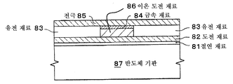
도 1은 미국 특허 제6,348,365호 명세서에 개시된 PCRAM의 구조를 도시하는 단면 개략도이다. 도 1에 도시하는 바와 같이 반도체 기판(87) 상에, 절연 재료(81), 도전 재료(82), 유전 재료(83)가 배치되고, 유전 재료(83)의 일부에 리세스 구조(홈 구조)가 형성되어 있다. 리세스 구조 중에 이온 도전 재료(86)와 금속 재료(84)가 배치되고, 전극(85)이 금속 재료(84)와 유전 재료(83) 위에 배치되어 있다. 전극(85)과 도전 재료(82)의 사이에 전압을 가하면, 덴드라이트라 불리는 전류로가 이온 도전 재료(86)의 표면에 형성되어, 전극(85)과 도전 재료(82)가 전기적으로 접속된다. 반대의 전압을 가하면, 덴드라이트는 없어져, 전극(85)과 도전 재료(82)가 전기적으로 절연된다.1 is a cross-sectional schematic diagram illustrating the structure of a PCRAM disclosed in US Pat. No. 6,348,365. As shown in FIG. 1, an insulating material 81, a conductive material 82, and a dielectric material 83 are disposed on the semiconductor substrate 87, and a recess structure (groove structure) is formed in a portion of the dielectric material 83. ) Is formed. The ion conductive material 86 and the metal material 84 are disposed in the recess structure, and the electrode 85 is disposed on the metal material 84 and the dielectric material 83. When a voltage is applied between the electrode 85 and the conductive material 82, a current path called dendrites is formed on the surface of the ion conductive material 86, and the electrode 85 and the conductive material 82 are electrically connected. do. When the opposite voltage is applied, the dendrite disappears and the electrode 85 and the conductive material 82 are electrically insulated.
제1 종래예의 안티퓨즈 소자는, FPL에서 주로 이용되고 있는 스위칭 소자로서, 온 상태일 때의 소자의 저항인 온 저항이 작기 때문에(50Ω 정도), 신호 지연 시간이 짧은 것이 특징이지만, 재프로그램을 할 수 없다고 하는 과제가 있다. 따라서, FPL을 프로그램할 때에, 디버그나, 동작중에 프로그램을 전환하고자 하는 등의 요청에 부응할 수 없다.The antifuse element of the first conventional example is a switching element mainly used in FPL, and is characterized by a short signal delay time because the on resistance, which is the resistance of the element in the on state, is small (around 50 µs), There is problem that we cannot do. Therefore, when programming an FPL, it cannot respond to requests such as debugging or switching programs during operation.
제2 종래예의 EEPROM은 재프로그램이 가능하지만, 현재로서는 집적도가 아직 작고, 또한 온 저항은 MOS(Metal Oxide Semiconductor) 트랜지스터의 저항으로 제한되기 때문에 수kΩ으로 크다. 불휘발성 메모리로서 널리 이용되고 있지만, 집적도는 절연막의 두께로 제한되어, 집적화가 더욱 어려워지고 있다. 또한, FPL에 이용했을 경우에는 큰 온 저항 때문에, 신호 지연이 발생한다는 문제가 있다.The EEPROM of the second conventional example is reprogrammable, but at present, the degree of integration is still small, and the on-resistance is large because it is limited to the resistance of a metal oxide semiconductor (MOS) transistor. Although widely used as a nonvolatile memory, the degree of integration is limited to the thickness of the insulating film, making integration more difficult. In addition, when used for FPL, there is a problem that a signal delay occurs due to a large on resistance.
제3 종래예의 타이머는, 전기 화학 반응인 전기 도금에 의해 전극이 용해할 때까지의 시간을 계측하는 장치이며, 스위칭 소자로서 온 상태와 오프 상태를 제어하여 전환할 수 없다.The timer of the third conventional example is an apparatus for measuring the time until the electrode dissolves by electroplating, which is an electrochemical reaction, and cannot be switched by controlling the on state and the off state as switching elements.
제4 종래예의 전자 소자에서는, 전기 화학 반응을 이용한 2단자 스위치를 기본으로 하고 있다. 온 상태와 오프 상태간의 천이는 2단자간에 인가하는 전압으로 제어한다. 상태간을 천이하는 경우에는 스위치에 전류가 흐르기 때문에, 소비 전력이 크다. 또한, 천이에 필요한 전류에 견디는 굵은 배선이나 구동력이 큰 트랜지스터가 필요하다. 스위치가 집적화 가능하다고 하여도, 배선이나 주변 회로를 집적화하는 것이 곤란하다.The electronic device of the fourth conventional example is based on a two-terminal switch using an electrochemical reaction. The transition between the on state and the off state is controlled by the voltage applied between the two terminals. When switching between states, current flows in the switch, so the power consumption is large. In addition, a thick wiring that withstands the current required for the transition and a transistor having a large driving force are required. Even if a switch can be integrated, it is difficult to integrate wiring and peripheral circuits.
<발명의 개시><Start of invention>
본 발명의 목적은 고집적화 가능하며, 전원을 끊어도 온 상태 및 오프 상태 중 어느 한쪽의 상태를 유지하고, 온 상태에서의 저항값이 낮으며, 또한 상기 어느 한쪽의 상태로 재프로그램이 가능한 스위칭 소자, 및 그 구동 방법, 그리고 스위칭 소자를 이용한 FPL 및 메모리 소자를 제공하는 것에 있다.SUMMARY OF THE INVENTION An object of the present invention is a switching element capable of high integration, which maintains either of the on state and the off state even when the power supply is turned off, and has a low resistance value in the on state, and is reprogrammable to either of the above states, And a driving method thereof, and an FPL and a memory element using a switching element.
본 발명의 스위칭 소자는 금속 이온이 전도될 수 있는 이온 전도체와, 이온 전도체에 접하여 배치된 제1 전극 및 제2 전극과, 이온 전도체에 접하여 배치되며 금속 이온을 포함하는 제3 전극을 구비하고, 제1 전극과 제2 전극의 전극 간 거리를 L1이라 하고, 제1 전극과 제3 전극의 전극 간 거리를 L2라 하고, 제2 전극과 제3 전극의 전극 간 거리를 L3이라 하면,The switching element of the present invention includes an ion conductor capable of conducting metal ions, a first electrode and a second electrode disposed in contact with the ion conductor, a third electrode disposed in contact with the ion conductor and including metal ions, When the distance between the electrodes of the first electrode and the second electrode is L1, the distance between the electrodes of the first electrode and the third electrode is L2, and the distance between the electrodes of the second electrode and the third electrode is L3,
L1<L2×2이고 L1<L3×2L1 <L2 × 2 and L1 <L3 × 2
의 식의 조건을 만족하는 것이다.The condition of the equation is satisfied.
본 발명에서는, 제3 전극에 인가하는 전압을 제어하여, 제1 전극과 제2 전극의 사이에 금속을 석출시키고, 석출한 금속을 용해시킬 수 있다. 그리고, 제1 전극과 제2 전극의 사이를 전기적으로 접속한 상태와, 전기적으로 접속되어 있지 않은 상태를 전환할 수 있다.In the present invention, the voltage applied to the third electrode can be controlled to deposit a metal between the first electrode and the second electrode, and dissolve the deposited metal. And the state which electrically connected between the 1st electrode and the 2nd electrode, and the state which is not electrically connected can be switched.
또한, 상기 본 발명의 스위칭 소자에 있어서, 제1 전극과 제2 전극의 전극 간 거리가 O.5㎛ 이하인 것으로 하여도 된다. 이 경우, 제1 전극과 제2 전극의 전극 간 거리를 O.5㎛ 이하로 함으로써, 다양한 집적 회로에 본 발명의 스위칭 소자를 내장할 수 있다.In the switching element of the present invention, the distance between the electrodes of the first electrode and the second electrode may be 0.5 µm or less. In this case, the switching element of the present invention can be incorporated into various integrated circuits by setting the distance between the electrodes of the first electrode and the second electrode to 0.5 m or less.
또한, 상기 본 발명의 스위칭 소자를, 절연막으로 덮인 기판 또는 절연성의 기판상에 형성하여도 된다. 이 경우의 일 형태로서, 제1 전극 및 제2 전극이 기판상에 이격 배치되어, 제1 전극과 제2 전극의 전극 간 거리가 O.5㎛ 이하이며, 이온 전도체가 제1 전극 및 제2 전극을 덮도록 배치되고, 제3 전극이 이온 전도체 상에 배치된 것으로 하여도 된다. 또한, 다른 형태로서, 제3 전극이 기판 상에 배치되고, 이온 전도체가 제3 전극 상에 배치되고, 제1 전극 및 제2 전극이 이온 전도체 상에 이격 배치되고, 제1 전극과 제2 전극의 전극 간 거리가 O.5㎛ 이하인 것으로 하여도 된다. 또한, 다른 형태로서, 제1 전극이 기판 상에 배치되고, 이온 전도체가 제1 전극 상에 배치되고, 제2 전극 및 제3 전극이 이온 전도체 상에 배치되고, 제1 전극과 제2 전극의 전극 간 거리가 이온 전도체의 막두께 이상인 것으로 하여도 된다. 이들 중 어느 하나의 구성으로 함으로써, 반도체 소자와 조합시킨 직접 회로 소자를 용이하게 형성할 수 있다.The switching element of the present invention may be formed on a substrate covered with an insulating film or an insulating substrate. In this case, the first electrode and the second electrode are spaced apart on the substrate, and the distance between the electrodes of the first electrode and the second electrode is 0.5 µm or less, and the ion conductor is formed of the first electrode and the second electrode. It may be arrange | positioned so that an electrode may be covered and a 3rd electrode may be arrange | positioned on an ion conductor. In another form, the third electrode is disposed on the substrate, the ion conductor is disposed on the third electrode, the first electrode and the second electrode are spaced apart on the ion conductor, and the first electrode and the second electrode are disposed. The distance between electrodes of may be 0.5 micrometer or less. In another form, the first electrode is disposed on the substrate, the ion conductor is disposed on the first electrode, the second electrode and the third electrode are disposed on the ion conductor, and the first electrode and the second electrode are The distance between the electrodes may be greater than or equal to the film thickness of the ion conductor. By setting it as any of these structures, the integrated circuit element combined with a semiconductor element can be formed easily.
또한, 상기 본 발명의 스위칭 소자에 있어서, 제3 전극에 전압이 인가됨으로써, 제1 전극과 제2 전극 사이의 전기 특성이 제어되는 것으로 하여도 된다. 이 경우, 전기 특성이 도전율이어도 된다.In addition, in the switching element of the present invention, the electrical characteristics between the first electrode and the second electrode may be controlled by applying a voltage to the third electrode. In this case, electrical conductivity may be sufficient.
또한, 상기 본 발명의 스위칭 소자에 있어서, 제1 전극 및 제2 전극 중 적어도 1개의 전극에 대해 제3 전극에 정(+)의 전압이 인가됨으로써, 제1 전극과 제2 전극의 사이가 전기적으로 접속된 상태인 온 상태가 형성되고, 제1 전극 및 제2 전극 중 적어도 1개의 전극에 대해 제3 전극에 부(-)의 전압이 인가됨으로써, 제1 전극과 제2 전극의 사이가 절연된 상태인 오프 상태가 형성되는 것으로 하여도 된다.In addition, in the switching element of the present invention, a positive voltage is applied to the third electrode to at least one of the first electrode and the second electrode, so that the first electrode and the second electrode are electrically connected. An on-state, which is in a connected state, is formed, and a negative voltage is applied to the third electrode with respect to at least one of the first electrode and the second electrode, thereby insulating between the first electrode and the second electrode. The off state which is a closed state may be formed.
또한, 상기 본 발명의 스위칭 소자에 있어서, 제2 전극이 전기 화학 반응에 의해 이온 전도체 중에 용해되는 금속을 포함하는 것으로 하여도 된다. 이 경우, 제1 전극에 대해 제2 전극에 정의 전압이 인가되거나, 또는 제1 전극 및 제2 전극 중 적어도 1개의 전극에 대해 제3 전극에 정의 전압이 인가됨으로써, 제1 전극과 제2 전극의 사이가 전기적으로 접속된 상태인 온 상태가 형성되고, 제1 전극에 대해 제2 전극에 부의 전압이 인가되거나, 또는 제1 전극 및 제2 전극 중 적어도 1개의 전극에 대해 제3 전극에 부의 전압이 인가됨으로써, 제1 전극과 제2 전극의 사이가 절연된 상태인 오프 상태가 형성되는 것으로 하여도 된다.In the switching element of the present invention, the second electrode may contain a metal dissolved in an ion conductor by an electrochemical reaction. In this case, a positive voltage is applied to the second electrode with respect to the first electrode, or a positive voltage is applied to the third electrode with respect to at least one of the first electrode and the second electrode, thereby providing the first electrode and the second electrode. An on-state is formed in which a state is electrically connected between and a negative voltage is applied to the second electrode with respect to the first electrode, or a negative voltage is applied to the third electrode with respect to at least one of the first electrode and the second electrode. By applying a voltage, an off state in which the first electrode and the second electrode are insulated from each other may be formed.
또한, 상기 본 발명의 스위칭 소자에 있어서, 제1 전극, 제2 전극 및 제3 전극 중 적어도 1개의 전극에 있어서, 이온 전도체에 접하는 면에 선예부(先銳部)를 갖는 것으로 하여도 된다.In the switching element of the present invention, at least one of the first electrode, the second electrode, and the third electrode may have a sharp portion on the surface in contact with the ion conductor.
또한, 상기 본 발명의 스위칭 소자에 있어서, 이온 전도체가, 원소의 주기율표에서의 6B족을 포함하는 칼코게나이드 재료, 금속 이온성 글래스, 또는 금속 이온성 비정질 반도체인 것으로 하여도 된다.In the switching element of the present invention, the ion conductor may be a chalcogenide material containing a Group 6B in the periodic table of the elements, a metal ionic glass, or a metal ionic amorphous semiconductor.
또한, 상기 본 발명의 스위칭 소자에 있어서, 이온 전도체와 제3 전극의 조합이 황화 구리와 구리, 또는 황화 은과 은의 조합이며, 제1 전극 및 제2 전극에 있어서, 이온 전도체와 접하는 부분이 백금, 알루미늄, 금, 티탄, 텅스텐, 바나듐, 니오븀, 탄탈, 크롬, 혹은 몰리브덴, 이들 금속의 질화물, 또는 이들 금속의 실리사이드, 혹은 이들 물질의 조합을 포함하는 것인 것으로 하여도 된다.Further, in the switching element of the present invention, the combination of the ion conductor and the third electrode is copper sulfide and copper, or the combination of silver sulfide and silver, and the portions of the first electrode and the second electrode in contact with the ion conductor are platinum. Or aluminum, gold, titanium, tungsten, vanadium, niobium, tantalum, chromium or molybdenum, nitrides of these metals, silicides of these metals, or combinations of these materials.
한편, 본 발명의 스위칭 소자의 구동 방법은, 상기 본 발명의 스위칭 소자에 있어서, 제3 전극에 인가하는 전압 및/또는 전압 인가 시간에 의해 전기 특성을 제 어하는 것이다.On the other hand, the driving method of the switching element of this invention WHEREIN: An electrical characteristic is controlled by the voltage and / or voltage application time applied to the 3rd electrode in the switching element of the said invention.
또한, 본 발명의 스위칭 소자의 구동 방법은, 상기 본 발명의 스위칭 소자에 있어서, 온 상태와 오프 상태를 제3 전극에 인가하는 전압의 극성에 의해 전환하고, 제3 전극으로의 전압을 정지함으로써 온 상태 또는 오프 상태를 유지하는 것이다. 이 경우, 온 상태와 오프 상태 간을 천이시킬 때, 제1 전극 및 제2 전극 간의 전도도를 측정하여, 전도도의 변화량에 의해 제3 전극에 인가하는 전압을 제어하는 것으로 하여도 된다.Moreover, in the switching element of the present invention, in the switching element of the present invention, the on state and the off state are switched by the polarity of the voltage applied to the third electrode, and the voltage to the third electrode is stopped. To stay on or off. In this case, when transitioning between the on state and the off state, the conductivity between the first electrode and the second electrode may be measured, and the voltage applied to the third electrode may be controlled by the amount of change in conductivity.
또한, 본 발명의 재기록 가능한 논리 집적 회로는, 상기 본 발명의 스위칭 소자를 프로그램용 스위치에 이용하는 구성이다.Moreover, the rewritable logic integrated circuit of this invention is a structure which uses the switching element of this invention for a program switch.
또한, 본 발명의 메모리 소자는 상기 본 발명의 스위칭 소자와, MOS 트랜지스터 또는 다이오드를 각각 1개씩 구비한 메모리 셀을 기본 단위로 하는 구성이다. 이 경우, 메모리 셀은 MOS 트랜지스터를 구비하며, 스위칭 소자는 제2 전극이 MOS 트랜지스터의 드레인 전극에 접속되고, 제1 전극이 제1 비트선에 접속되고, 제3 전극이 제1 워드선에 접속되며, MOS 트랜지스터는, 소스 전극이 제1 비트선과 상이한 제2 비트선에 접속되고, 게이트 전극이 제1 워드선과 상이한 제2 워드선에 접속된 것으로 하여도 된다.The memory element of the present invention is a configuration in which the switching element of the present invention and the memory cell each including one MOS transistor or diode are provided as basic units. In this case, the memory cell includes a MOS transistor, in which the second electrode is connected to the drain electrode of the MOS transistor, the first electrode is connected to the first bit line, and the third electrode is connected to the first word line. The MOS transistor may be configured such that the source electrode is connected to a second bit line different from the first bit line, and the gate electrode is connected to a second word line different from the first word line.
또한, 본 발명의 스위칭 소자는 전기 화학 반응을 이용한 스위칭 소자로서, 전기 화학 반응에 이용되는 금속 이온이 전도되기 위한 이온 전도체와, 이온 전도체에 접하고 소정의 거리만큼 떨어져 형성된 제1 전극 및 제2 전극과, 스위칭 소자를 온 상태로 천이시키는 전압이 인가되면 제1 전극 및 제2 전극의 사이에 금속 이 온에 의한 금속을 석출시켜 제1 전극 및 제2 전극을 전기적으로 접속하고, 스위칭 소자를 오프 상태로 천이시키는 전압이 인가되면 석출된 금속을 용해시켜 제1 전극 및 제2 전극의 전기적 접속을 끊기 위한, 이온 전도체에 접하여 형성된 제3 전극을 갖는 구성이다.In addition, the switching device of the present invention is a switching device using an electrochemical reaction, the ion conductor for conducting the metal ions used in the electrochemical reaction, the first electrode and the second electrode formed in contact with the ion conductor separated by a predetermined distance And a voltage for transitioning the switching element to an on state is applied to deposit a metal by metal ions between the first electrode and the second electrode to electrically connect the first electrode and the second electrode, and to turn off the switching element. It is a structure which has a 3rd electrode formed in contact with an ion conductor, when the voltage which makes a transition to a state is applied, and the deposited metal is dissolved and the electric connection of a 1st electrode and a 2nd electrode is disconnected.
본 발명에서는, 스위칭 소자를 온 상태로 하기 위한 전압을 제3 전극에 인가하면, 전기 화학 반응에 의해 이온 전도체내를 금속 이온이 제1 전극 및 제2 전극으로 끌어 당겨져 이들 전극 표면에 금속이 석출되고, 제1 전극과 제2 전극의 사이에 석출된 금속이 양 전극을 전기적으로 접속한다. 또한, 스위칭 소자를 오프 상태로 하기 위한 전압을 제3 전극에 인가하면, 제1 전극과 제2 전극의 사이에 석출된 금속이 금속 이온으로 되어 이온 전도체 중에 용해되어, 제1 전극과 제2 전극의 전기적 접속이 끊어진다. 또한, 온 상태에서는, 제1 전극과 제2 전극이 금속으로 접속되기 때문에, 제1 전극 및 제2 전극 간의 저항값이 보다 작아진다.In the present invention, when a voltage for turning on the switching element is applied to the third electrode, metal ions are attracted to the first electrode and the second electrode in the ion conductor by the electrochemical reaction, and the metal precipitates on the surface of these electrodes. The metal deposited between the first electrode and the second electrode electrically connects both electrodes. When a voltage for turning off the switching element is applied to the third electrode, the metal precipitated between the first electrode and the second electrode becomes metal ions and is dissolved in the ion conductor, so that the first electrode and the second electrode are dissolved. The electrical connection of the is disconnected. In the on-state, since the first electrode and the second electrode are connected by metal, the resistance value between the first electrode and the second electrode becomes smaller.
또한, 상기 본 발명의 스위칭 소자에 있어서, 스위칭 소자가 온 상태 또는 오프 상태로 된 후, 제3 전극으로의 전압의 인가가 정지되어도, 그 상태를 유지하는 것으로 하여도 된다.In the switching element of the present invention, after the switching element is turned on or off, the state may be maintained even if the application of the voltage to the third electrode is stopped.
본 발명에서는, 스위칭 소자를 온 상태로 한 후, 제3 전극에 전압을 인가하지 않아도, 석출된 금속에 의해 제1 전극과 제2 전극이 전기적으로 접속된 상태가 유지된다. 또한, 스위칭 소자를 오프 상태로 한 후, 제3 전극에 전압을 인가하지 않아도, 제1 전극과 제2 전극의 전기적 접속이 끊어진 상태가 유지된다. 그 때문에, 온 상태 또는 오프 상태의 정보를 보유한 불휘발성을 갖게 된다.In the present invention, after the switching element is turned on, even when no voltage is applied to the third electrode, a state in which the first electrode and the second electrode are electrically connected by the deposited metal is maintained. In addition, after the switching element is turned off, the state in which the electrical connection between the first electrode and the second electrode is cut off is maintained even when no voltage is applied to the third electrode. Therefore, there is a non-volatile having information of the on state or the off state.
또한, 본 발명의 스위칭 소자는 전기 화학 반응을 이용한 스위칭 소자로서, 전기 화학 반응에 이용되는 금속 이온이 전도되기 위한 이온 전도체와, 이온 전도체에 접하여 형성된 제1 전극과, 스위칭 소자를 온 상태로 천이시키는 전압이 인가되면 금속 이온에 의한 금속을 석출시켜 제1 전극과 전기적으로 접속되고, 스위칭 소자를 오프 상태로 천이시키는 전압이 인가되면 석출된 금속을 용해시켜 제1 전극과의 전기적 접속이 끊기는, 이온 전도체에 접하고 제1 전극과 소정의 거리만큼 떨어져 설치된 제2 전극과, 제1 전극에 대해 정의 전압이 인가되면 제1 전극 및 제2 전극 간의 전류를 증가시키고, 제1 전극에 대해 부의 전압이 인가되면 전류를 감소시키기 위한, 이온 전도체에 접하여 설치된 제3 전극을 갖는 구성이다.In addition, the switching element of the present invention is a switching element using an electrochemical reaction, an ion conductor for conducting metal ions used in the electrochemical reaction, a first electrode formed in contact with the ion conductor, and the switching element transitions to an on state When a voltage to be applied is applied to deposit a metal by metal ions and is electrically connected to the first electrode, and when a voltage is applied to switch the switching element to an off state, the deposited metal is dissolved and the electrical connection with the first electrode is cut off. When a positive voltage is applied to the second electrode in contact with the ion conductor and spaced apart from the first electrode by a predetermined distance, the current between the first electrode and the second electrode is increased, and a negative voltage is applied to the first electrode. It is a configuration having a third electrode provided in contact with the ion conductor to reduce the current when applied.
본 발명에서는, 스위칭 소자를 온 상태로 하기 위한 전압을 제2 전극에 인가하면, 전기 화학 반응에 의해 이온 전도체 내를 금속 이온이 제1 전극으로 끌어 당겨져 전극 표면에 금속이 석출되고, 제1 전극과 제2 전극의 사이에 석출된 금속이 양 전극을 전기적으로 접속한다. 그리고, 제1 전극에 대해 정의 전압을 제3 전극에 인가함으로써, 제1 전극과 제2 전극의 사이에 석출되는 금속의 양이 증가하여, 전류가 증가한다. 또한, 스위칭 소자가 온 상태로 된 후, 제1 전극에 대해 부의 전압을 제3 전극에 인가함으로써, 제1 전극과 제2 전극의 사이에 석출된 금속의 양이 줄어들어, 전류가 감소한다. 그리고, 스위칭 소자를 오프 상태로 하기 위한 전압을 제2 전극에 인가하면, 제1 전극과 제2 전극의 사이에 석출된 금속이 금속 이온으로 되어 이온 전도체 중에 용해되어, 제1 전극과 제2 전극의 전기적 접속이 끊어진다. 그 때문에, 제2 전극에 전압을 인가함으로써 온 상태 및 오프 상태를 제 어 가능할 뿐만 아니라, 제3 전극에 전압을 인가함으로써 전류의 크기를 제어할 수 있다.In the present invention, when a voltage for turning on the switching element is applied to the second electrode, metal ions are attracted to the first electrode in the ion conductor by the electrochemical reaction, and the metal is deposited on the electrode surface. The metal deposited between the second electrode and the second electrode electrically connects both electrodes. Then, by applying a positive voltage to the third electrode with respect to the first electrode, the amount of metal precipitated between the first electrode and the second electrode increases, and the current increases. Further, after the switching element is turned on, by applying a negative voltage to the third electrode with respect to the first electrode, the amount of metal deposited between the first electrode and the second electrode is reduced, and the current is reduced. When a voltage for turning off the switching element is applied to the second electrode, the metal precipitated between the first electrode and the second electrode becomes metal ions and is dissolved in the ion conductor, so that the first electrode and the second electrode are dissolved. The electrical connection of the is disconnected. Therefore, not only the on state and the off state can be controlled by applying a voltage to the second electrode, but also the magnitude of the current can be controlled by applying a voltage to the third electrode.
또한, 본 발명의 스위칭 소자는 전기 화학 반응을 이용한 스위칭 소자로서, 전기 화학 반응에 이용되는 금속 이온이 전도되기 위한 이온 전도체와, 이온 전도체에 접하여 형성된 제1 전극과, 소정의 전압이 소정의 시간 인가되면 금속 이온에 의한 금속이 석출되는, 이온 전도체에 접하고 제1 전극과 소정의 거리만큼 떨어져 형성된 제2 전극과, 제2 전극에 소정의 전압이 소정의 시간 인가된 후, 스위칭 소자를 온 상태로 천이시키는 전압이 인가되면 금속 이온에 의한 금속을 석출시켜 제1 전극과 제2 전극을 전기적으로 접속하기 위한, 이온 전도체에 접하여 설치된 제3 전극을 갖는 구성이다.In addition, the switching element of the present invention is a switching element using an electrochemical reaction, an ion conductor for conducting metal ions used in the electrochemical reaction, a first electrode formed in contact with the ion conductor, a predetermined voltage is a predetermined time When applied, the switching electrode is turned on after a predetermined voltage is applied to the second electrode and the second electrode formed in contact with the ion conductor and separated from the first electrode by a predetermined distance. When a voltage to be transferred to is applied, a third electrode provided in contact with the ion conductor for depositing metal by metal ions to electrically connect the first electrode and the second electrode.
본 발명에서는, 제1 전극과 제2 전극이 전기 화학 반응에 의해 석출되는 금속으로 접속되기 전까지 제2 전극에 전압을 인가한 후, 스위칭 소자를 온 상태로 하기 위한 전압을 제3 전극에 인가함으로써, 제1 전극과 제2 전극을 전기적으로 접속하고 있다. 그 때문에, 제1 전극과 제2 전극이 전기적으로 접속될 때에 전류가 과잉으로 흐르는 것을 방지하여, 소비 전력이 억제된다.In the present invention, by applying a voltage to the second electrode before the first electrode and the second electrode is connected to the metal precipitated by the electrochemical reaction, by applying a voltage for turning on the switching element to the third electrode The first electrode and the second electrode are electrically connected. Therefore, excessive current flow is prevented when the first electrode and the second electrode are electrically connected, and power consumption is suppressed.
또한, 상기 본 발명의 스위칭 소자에 있어서, 제3 전극은 이온 전도체에 금속 이온을 공급하기 위한 재료를 포함하고, 제1 전극 및 제2 전극이 이온 전도체와 접하는 부위는 이온 전도체와 반응하지 않는 재료인 것으로 하여도 된다.Further, in the switching element of the present invention, the third electrode includes a material for supplying metal ions to the ion conductor, and a portion where the first electrode and the second electrode contact the ion conductor does not react with the ion conductor. You may be that.
본 발명에서는, 전기 화학 반응에 의해 제3 전극으로부터 금속 이온이 이온 전도체에 공급되기 때문에, 이온 전도도가 커져, 상태 간의 천이 속도가 더욱 커진 다.In the present invention, since metal ions are supplied to the ion conductor from the third electrode by the electrochemical reaction, the ion conductivity is increased, and the transition speed between the states is further increased.
또한, 상기 본 발명의 스위칭 소자에 있어서, 제3 전극 및 제2 전극은 이온 전도체에 금속 이온을 공급하기 위한 재료를 포함하고, 제1 전극이 이온 전도체와 접하는 부위는 이온 전도체와 반응하지 않는 재료인 것으로 하여도 된다.Further, in the switching element of the present invention, the third electrode and the second electrode include a material for supplying metal ions to the ion conductor, and the portion where the first electrode is in contact with the ion conductor does not react with the ion conductor. You may be that.
본 발명에서는, 전기 화학 반응에 의해 제3 전극 및 제2 전극으로부터 금속 이온이 이온 전도체에 공급되기 때문에, 이온 전도도가 커져, 상태간의 천이 속도가 더욱 커진다.In the present invention, since metal ions are supplied to the ion conductor from the third electrode and the second electrode by the electrochemical reaction, the ion conductivity is increased, and the transition speed between the states is further increased.
또한, 상기 본 발명의 스위칭 소자에 있어서, 제1 전극 및 제2 전극이 제3 전극의 평면 패턴에 대해 평행한 동일 평면내에 형성되고, 제1 전극 및 제2 전극 중 적어도 어느 한쪽의 평면 패턴에 첨예부를 갖고, 제1 전극과 제2 전극의 최단 거리가 한쪽 전극의 첨예부로부터 다른쪽의 전극까지의 거리로 표현되는 것으로 하여도 된다.Further, in the switching element of the present invention, the first electrode and the second electrode are formed in the same plane parallel to the plane pattern of the third electrode, and in at least one plane pattern of the first electrode and the second electrode. You may have a sharp part and the shortest distance of a 1st electrode and a 2nd electrode may be represented by the distance from the sharp part of one electrode to the other electrode.
본 발명에서는, 2개의 전극 간의 최단 거리가 한쪽의 전극에서의 첨예부로부터 다른쪽의 전극까지의 거리가 되기 때문에, 그 첨예부를 갖는 쪽의 전극에서는 적어도 첨예부 부근에 구리가 석출됨으로써 다른 한쪽의 전극과 전기적으로 접속 가능해져, 여분의 구리의 석출을 필요로 하지 않고, 오프 상태로부터 온 상태로의 천이 속도가 더욱 커진다. 또한, 스위칭 소자를 오프 상태로 하는 경우, 상기 첨예부 부근의 금속이 용해되면 되기 때문에, 온 상태로부터 오프 상태로의 천이 속도도 커진다.In the present invention, since the shortest distance between two electrodes becomes the distance from the sharpened part in one electrode to the other electrode, copper is deposited at least near the sharpened part in the electrode having the sharpened part, It becomes electrically connectable with an electrode, and does not require the precipitation of extra copper, and the transition speed from an OFF state to an ON state becomes further larger. In the case where the switching element is turned off, the metal near the sharp portion needs to be dissolved, so that the transition speed from the on state to the off state also increases.
한편, 상기 목적을 달성하기 위한 본 발명의 재기록 가능한 논리 집적 회로 는, 상기 본 발명의 스위칭 소자 중 어느 하나를 프로그램용 소자에 이용한 구성이다. 본 발명에서는, 프로그램용 소자로서 이용한 스위칭 소자를 온 상태 또는 오프 상태로 천이시킴으로써, 논리 회로를 자유롭게 설정할 수 있다.On the other hand, the rewritable logic integrated circuit of the present invention for achieving the above object is a configuration in which any one of the switching elements of the present invention is used for a program element. In the present invention, the logic circuit can be freely set by transitioning the switching element used as the program element to an on state or an off state.
또한, 상기 목적을 달성하기 위한 본 발명의 메모리 소자는, 상기 본 발명의 스위칭 소자 중 어느 하나와, 스위칭 소자가 온 상태 및 오프 상태 중 어느 상태인지를 읽어내기 위한 트랜지스터를 갖는 구성이다. 본 발명에서는, 전기 화학 반응을 이용하여 스위칭 소자를 온 상태 또는 오프 상태로 한 후, 제3 전극 및 제2 전극에 전압을 인가하지 않아도 그 상태가 유지되기 때문에, 불휘발성 메모리로서 이용할 수 있다.Moreover, the memory element of this invention for achieving the said objective is a structure which has a transistor for reading out any one of the said switching element of this invention, and a state in which a switching element is an on state and an off state. In the present invention, after the switching element is turned on or off using an electrochemical reaction, the state is maintained even when no voltage is applied to the third electrode and the second electrode, so that the switching element can be used as a nonvolatile memory.
따라서, 본 발명에 따르면, 제3 전극 및 제2 전극중 중 적어도 어느 한쪽에 소정의 전압을 인가함으로써 온 상태 또는 오프 상태로 임의로 설정 가능하고, 불휘발성이며, 또한 온 상태의 저항값이 보다 작은 스위칭 소자를 제공할 수 있다. 또한, 본 발명의 스위칭 소자는 구조가 간편하고 미세하기 때문에, 종래보다도 훨씬 미세화가 가능하다.Therefore, according to the present invention, by applying a predetermined voltage to at least one of the third electrode and the second electrode, it can be arbitrarily set in the on state or the off state, is nonvolatile, and the resistance value of the on state is smaller. A switching element can be provided. In addition, since the switching element of the present invention is simple and fine in structure, the switching element of the present invention can be further refined than before.
또한, 본 발명의 스위칭 소자를 FPL에 사용하면, 재프로그램 가능하면서, 또한 동작 속도가 큰 FPL을 제공할 수 있다.In addition, the use of the switching element of the present invention in an FPL can provide a reprogrammable FPL with a high operating speed.
또한, 본 발명의 스위칭 소자를 메모리 소자의 정보 기억 수단에 사용하면, 기입·판독 속도가 빠른 불휘발성 메모리 소자를 제공할 수 있다. 그리고, 본 발명의 스위칭 소자는 구조가 간편하고 미세하기 때문에, 고집적이며 고속인 메모리 집적 회로를 제공할 수 있다.Moreover, when the switching element of this invention is used for the information storage means of a memory element, a nonvolatile memory element with a high writing and reading speed can be provided. In addition, since the switching element of the present invention is simple and fine in structure, it is possible to provide a highly integrated and high speed memory integrated circuit.
또한, 본 발명의 제조 방법에 의하면, 종래의 반도체 집적 회로의 제조 기술을 적용하여 정밀도 좋고, 재현성 좋게 제조할 수 있다. 따라서, 스위칭 소자 및 그것을 이용한 FPL이나 메모리 소자 등의 집적 회로를 저비용으로 제공할 수 있다.Moreover, according to the manufacturing method of this invention, it can manufacture with good precision and reproducibility by applying the conventional manufacturing technology of a semiconductor integrated circuit. Therefore, a switching element and an integrated circuit such as an FPL or a memory element using the same can be provided at low cost.
도 1은 제4 종래예의 전자 소자의 구성을 도시하는 단면 개략도.BRIEF DESCRIPTION OF THE DRAWINGS Fig. 1 is a schematic cross sectional view showing a configuration of an electronic device of a fourth conventional example.
도 2는 본 발명의 스위칭 소자의 일 구성예를 도시하는 단면도.2 is a cross-sectional view showing a configuration example of a switching element of the present invention.
도 3a는 본 발명의 스위칭 소자의 전기 특성을 나타내는 그래프.Figure 3a is a graph showing the electrical characteristics of the switching element of the present invention.
도 3b는 본 발명의 스위칭 소자의 전기 특성을 나타내는 그래프.3B is a graph showing electrical characteristics of the switching device of the present invention.
도 4는 본 발명의 스위칭 소자의 전기 화학 반응을 설명하기 위한 도면.4 is a view for explaining the electrochemical reaction of the switching device of the present invention.
도 5는 본 발명의 스위칭 소자의 일 구성예를 도시하는 단면도.Fig. 5 is a sectional view showing one configuration example of a switching element of the present invention.
도 6a는 소스 전극 및 드레인 전극의 평면 패턴의 일례를 도시하는 평면 모식도.6A is a plan schematic diagram illustrating an example of a planar pattern of a source electrode and a drain electrode.
도 6b는 소스 전극 및 드레인 전극의 평면 패턴의 일례를 도시하는 평면 모식도.6B is a plan schematic diagram illustrating an example of a planar pattern of the source electrode and the drain electrode.
도 7은 게이트 전압을 피드백 제어하기 위한 플로우차트.7 is a flowchart for feedback control of a gate voltage.
도 8a는 제1 실시예의 스위칭 소자의 다른 구조를 도시하는 단면도.8A is a sectional view showing another structure of the switching element of the first embodiment.
도 8b는 제1 실시예의 스위칭 소자의 다른 구조를 도시하는 단면도.8B is a sectional view showing another structure of the switching element of the first embodiment.
도 8c는 제1 실시예의 스위칭 소자의 다른 구조를 도시하는 단면도.8C is a sectional view showing another structure of the switching element of the first embodiment.
도 9는 이온 전도체에 양극 분극법에 의해 제작한 황화 구리를 이용한 제1 실시예의 스위칭 소자의 전기 특성을 나타내는 그래프.Fig. 9 is a graph showing the electrical characteristics of the switching element of the first embodiment using copper sulfide produced by the anode polarization method for the ion conductor.
도 10은 이온 전도체에 레이저 어블레이션법에 의해 제작한 황화 구리를 이용한 제1 실시예의 스위칭 소자의 전기 특성을 나타내는 그래프.Fig. 10 is a graph showing the electrical characteristics of the switching element of the first embodiment using copper sulfide produced by laser ablation for an ion conductor.
도 11은 제2 실시예의 스위칭 소자의 구성을 도시하는 단면도.11 is a sectional view showing a configuration of a switching element of a second embodiment.
도 12는 FPL에 적용한 본 발명의 스위칭 소자의 일 구성예를 도시하는 단면도.12 is a cross-sectional view showing one configuration example of a switching element of the present invention applied to an FPL.
도 13은 본 발명의 스위칭 소자와 MOS 트랜지스터를 이용한 메모리 소자를 나타내는 회로도. Fig. 13 is a circuit diagram showing a memory device using the switching device and the MOS transistor of the present invention.
본 발명의 스위칭 소자의 특징은 다음과 같다. 제3 전극에 인가하는 전압을 제어하여 제1 전극과 제2 전극의 사이에 금속을 석출시킴으로써, 제1 전극과 제2 전극의 사이가 전기적으로 접속된 상태, 즉 온 상태로 한다. 또한, 제1 전극과 제2 전극의 사이에 석출된 금속을 용해시킴으로써 제1 전극과 제2 전극의 사이가 전기적으로 접속되어 있지 않은 상태, 즉 오프 상태로 한다. 또한, 각 상태는 제3 전극에 전압을 인가하는 것을 멈추어도 유지된다.Features of the switching device of the present invention are as follows. By controlling the voltage applied to the third electrode and depositing a metal between the first electrode and the second electrode, the state between the first electrode and the second electrode is in an electrically connected state, that is, an on state. In addition, by dissolving the metal deposited between the first electrode and the second electrode, the state between the first electrode and the second electrode is not electrically connected, that is, turned off. In addition, each state is maintained even if it stops applying a voltage to a 3rd electrode.
본 발명의 구성에 대해 설명한다. 또, 이하의 설명, 그리고 도 2, 도 3a, 도 3b, 도 5, 도 6a, 도 6b, 도 8a, 도 8b, 도 8c, 도 9, 도 10, 도 11 및 도 12에 있어서, 제1 전극이 소스 전극에 대응하고, 제2 전극이 드레인 전극에 대응하고, 제3 전극이 게이트 전극에 대응한다.The structure of this invention is demonstrated. In addition, in the following description and FIG. 2, FIG. 3A, FIG. 3B, FIG. 5, FIG. 6A, FIG. 6B, FIG. 8A, FIG. 8B, FIG. 8C, FIG. 9, FIG. 10, FIG. 11, and FIG. The electrode corresponds to the source electrode, the second electrode corresponds to the drain electrode, and the third electrode corresponds to the gate electrode.
도 2는 본 발명의 스위칭 소자의 일 구성예를 도시하는 단면도이다.2 is a cross-sectional view showing one configuration example of a switching element of the present invention.
도 2에 도시하는 바와 같이, 본 발명의 스위칭 소자는 절연막으로서 실리콘 산화막이 실리콘 기판에 피복된 기판(5) 상에 소정의 거리를 두고 형성된 소스 전극(1) 및 드레인 전극(2)과, 소스 전극(1) 및 드레인 전극(2)에 접하여 설치되고, 전기 화학 반응을 위한 금속 이온을 포함한 이온 전도체(4)와, 이온 전도체(4) 상에 형성된 게이트 전극(3)을 갖는다. 게이트 전극(3)은 인가되는 전압의 크기에 따라, 소스 전극(1) 및 드레인 전극(2) 사이의 전도도를 제어하기 위한 것이다. 소스 전극(1), 드레인 전극(2) 및 게이트 전극(3)은 서로 전기적으로 절연된 상태로 배치되어 있다.As shown in Fig. 2, the switching element of the present invention comprises a
게이트 전극(3)은 전기 화학 반응에 의해 이온 전도체(4)에 금속 이온을 공급하기 위한 재료를 포함하고 있다. 소스 전극(1) 및 드레인 전극(2)의 이온 전도체(4)와 접하는 부위에는 전기 화학 반응에 의해 이온 전도체(4)와 반응하지 않는 재료가 이용되고 있기 때문에, 소스 전극(1) 및 드레인 전극(2)은 금속 이온을 공급하지 않는다.The gate electrode 3 contains a material for supplying metal ions to the ion conductor 4 by an electrochemical reaction. Since the material which does not react with the ion conductor 4 by the electrochemical reaction is used in the site | part which contact | connects the ion conductor 4 of the
상기 구성의 스위칭 소자의 동작에 대해 설명한다.The operation of the switching element of the above configuration will be described.
소스 전극(1) 및 드레인 전극(2)에 대해 게이트 전극(3)에 정의 전압을 인가하면, 근접하는 소스 전극(1) 및 드레인 전극(2) 상에 금속 이온의 환원 반응에 의해 금속이 석출된다. 그리고, 소스 전극(1) 및 드레인 전극(2) 사이에 형성된 소정의 거리인 전극 간의 갭(6)에 석출된 금속 때문에 소스 전극(1) 및 드레인 전극(2)이 전기적으로 접속되어, 스위치는 온 상태로 천이한다. 한편, 소스 전극(1) 및 드레인 전극(2)에 대해 게이트 전극(3)에 부의 전압을 인가하면, 전극 간의 갭(6)에 있어서 석출된 금속이 산화되어 금속 이온으로 되어 이온 전도체(4) 중에 용 해하여, 전극 간의 갭(6)의 금속이 제거되어 오프 상태로 천이한다. 또, 이 전극 간의 갭(6)은 소스 전극(1) 및 드레인 전극(2) 간의 거리의 최단부로 된다.When a positive voltage is applied to the gate electrode 3 with respect to the
이들 온 상태 및 오프 상태는, 게이트 전극(3)에 전압을 인가하는 것을 멈추어도 각각의 상태가 유지된다. 또한, 온 상태의 후, 게이트 전극(3)에 인가하는 전압의 인가 시간 및 인가 전압에 따라 금속이 석출 또는 용해되어, 게이트 전극(3)에 인가하는 전압에 의해 소스 전극(1) 및 드레인 전극(2) 간의 전도도를 제어 가능하게 된다.These on-states and off-states are maintained even when the voltage is applied to the gate electrode 3. After the on state, the metal is deposited or dissolved in accordance with the application time of the voltage applied to the gate electrode 3 and the applied voltage, and the
여기에서, 소스 전극(1)과 드레인 전극(2)의 전극 간 거리를 L1이라 하고, 소스 전극(1)과 게이트 전극(3)의 전극 간 거리를 L2라 하고, 드레인 전극(2)과 게이트 전극(3)의 전극 간 거리를 L3이라 하면, 하기 수학식 1의 조건을 만족하도록 소스 전극(1), 드레인 전극(2) 및 게이트 전극(3)을 배치하는 것이 가능하다.Here, the distance between the electrodes of the
수학식 1의 조건을 만족하도록 구성함으로써, 소스 전극(1) 및 드레인 전극(2)의 양쪽으로부터 금속을 성장시키는 경우, 성장한 금속에 의해 소스 전극-드레인 전극 간이 전기적으로 접속된 상태가 형성되기 전에, 소스 전극-게이트 전극 간 또는 드레인 전극-게이트 전극이 전기적으로 접속된 상태가 형성되는 것을 거의 회피할 수 있었다.When the metal is grown from both the
또한, 하기 수학식 2의 조건을 만족하도록 소스 전극(1), 드레인 전극(2) 및 게이트 전극(3)을 배치하여도 된다.In addition, the
수학식 2의 조건을 만족하도록 구성함으로써, 소스 전극 및 드레인 전극중 어느 한쪽으로부터 금속을 성장시키는 경우에서도, 성장한 금속에 의해 소스 전극-드레인 전극 간이 전기적으로 접속된 상태가 형성되기 전에, 소스 전극-게이트 전극 간 또는 드레인 전극-게이트 전극이 전기적으로 접속된 상태가 형성되는 것을 거의 회피할 수 있었다. 또한, 소스 전극(1)과 드레인 전극(2) 사이의 도전율을 게이트 전극(3)에 인가하는 전압에 의해 제어하고자 하는 경우에, 수학식 2의 조건을 만족하는 구성으로 함으로써, 게이트 전극에 인가하는 전압의 가변 마진을 크게 할 수 있다.By constructing to satisfy the condition of
또한, 하기 수학식 3의 조건을 만족하도록 소스 전극(1), 드레인 전극(2), 및 게이트 전극(3)을 배치하여도 된다.In addition, the
수학식 3의 조건을 만족하도록 구성함으로써, 소스 전극 및/또는 드레인 전극으로부터 성장한 금속에 의해 소스 전극-게이트 전극 간 또는 드레인 전극-게이트 전극이 전기적으로 접속된 상태가 형성되는 것을 확실하게 회피할 수 있었다.By configuring to satisfy the condition of equation (3), it is possible to reliably avoid the formation of a state in which the source electrode and / or the gate electrode are electrically connected by the metal grown from the source electrode and / or the drain electrode. there was.
소스 전극(1)과 드레인 전극(2)의 전극 간 거리인 L1이 짧을수록, 게이트 전극(3)에 인가하는 전압을 작게 할 수 있어, 소자의 소비 전력을 작게 할 수 있다. 또한, 스위치 온 상태와 스위치 오프 상태의 전환 속도도 빠르게 할 수 있다. L1 을 0.5㎛ 이하로 함으로써, 다양한 집적 회로에 본 발명의 스위칭 소자를 내장할 수 있다. 한편, L1을 지나치게 짧게 하면, 단순하게 소스 전극-드레인 전극 간에 전압을 걸었을 때에 흐르는 누설 전류가 커진다. 소스 전극-드레인 전극에 흐르는 전류값의 1/10 이하로 누설 전류가 되도록 L1을 설정하여도 된다.As the distance L1 between the electrodes of the
다음으로, 도 2에 도시한 스위칭 소자의 전기 특성에 대해 설명한다.Next, the electrical characteristics of the switching element shown in FIG. 2 are demonstrated.
도 3a 및 도 3b는 스위칭 소자의 전기 특성을 나타내는 그래프이다. 도 3a 및 도 3b에 나타내는 그래프의 횡축은 도 2의 스위칭 소자의 게이트 전극(3)에 인가되는 전압인 게이트 전압을 나타내고, 종축은 소스 전극(1) 및 드레인 전극(2)의 사이에 흐르는 전류인 드레인 전류를 나타낸다.3A and 3B are graphs showing electrical characteristics of the switching element. 3A and 3B, the horizontal axis represents a gate voltage which is a voltage applied to the gate electrode 3 of the switching element of FIG. 2, and the vertical axis represents a current flowing between the
도 3a의 실측에 이용한 스위칭 소자는, 이온 전도체(4)가 황화 구리 수용액이며, 소스 전극(1) 및 드레인 전극(2)은 이온 전도체(4)에 용해되지 않는 백금(Pt)으로 형성되고, 게이트 전극(3)은 이온 전도체(4)와 전기 화학 반응을 나타내는 구리(Cu)로 형성되어 있다.In the switching element used for the actual measurement of FIG. 3A, the ion conductor 4 is an aqueous copper sulfide solution, and the
도 3a에 나타내는 바와 같이, 드레인 전극(2)과 소스 전극(1) 사이의 전압을 일정하게 하고, 게이트 전극(3)과 소스 전극(1) 사이의 전위차를 소정의 범위에서 반복하여 증감시키면, 드레인 전극(2)과 소스 전극(1) 사이의 전도도가 히스테리시스를 나타내는 것을 알 수 있다. 이하에, 그것을 상세하게 설명한다.As shown in FIG. 3A, when the voltage between the
전압을 인가하지 않는 초기 상태에서는 드레인 전류가 거의 흐르지 않는 오프 상태이다. 이 오프 상태로부터 게이트 전극(3)에 인가하는 게이트 전압을 0V에서부터 정의 방향으로 +0.3V까지 변화시키면, 드레인 전류가 약 1.2mA 흘러 스위칭 소자가 온 상태로 천이한다. 계속하여, 온 상태로부터 게이트 전압을 부의 방향으로 -0.16V까지 변화시키면, 드레인 전류가 거의 흐르지 않게 되어, 스위칭 소자가 오프 상태로 천이한다. 이와 같이, 게이트 전압이 -0.16V와 +0.3V의 사이에서는 천이는 일어나지 않고, 온 상태 또는 오프 상태가 안정적으로 존재한다. 또한, 게이트 전압을 반복하여 증감시킴으로서, 스위칭 소자를 온 상태와 오프 상태의 사이에서 몇번이라도 천이시키는 것이 가능하다.In the initial state where no voltage is applied, the drain current is in an off state where little drain current flows. When the gate voltage applied to the gate electrode 3 from this off state is changed from 0V to + 0.3V in the positive direction, the drain current flows about 1.2 mA and the switching element transitions to the on state. Subsequently, when the gate voltage is changed from the on state to -0.16 V in the negative direction, almost no drain current flows, and the switching element transitions to the off state. In this way, no transition occurs between the gate voltage of -0.16V and + 0.3V, and the on state or the off state exists stably. Further, by repeatedly increasing and decreasing the gate voltage, it is possible to make the switching element transition any number of times between the on state and the off state.
다음으로, 전술한 도 3a에 있어서 온 상태와 오프 상태의 천이가 생기는 이유를 설명한다.Next, the reason why the transition between the on state and the off state occurs in FIG. 3A described above will be described.
도 4는 전기 화학 반응에 의한 구리의 석출 및 용해를 설명하기 위한 모식도이다.4 is a schematic diagram for explaining precipitation and dissolution of copper by an electrochemical reaction.
도 4에 도시하는 바와 같이, 황산 구리와 황산의 혼합 용액의 이온 전도체에 금전극과 구리 전극을 침지하고, 구리 전극측을 정극, 금전극측을 부극으로 하여 전압원에 의해 전압을 인가한다. 상기 혼합 용액은 구리 도금액이기 때문에, 정극의 구리 전극에서는 구리가 구리 이온으로 되어 이온 전도체에 용해되고, 부극의 금전극에서는 구리가 석출된다. 이와 같은 전기 화학 반응에 의해 구리의 석출 및 용해가 일어난다.As shown in Fig. 4, a gold electrode and a copper electrode are immersed in an ion conductor of a mixed solution of copper sulfate and sulfuric acid, and a voltage is applied by a voltage source with the copper electrode side as the positive electrode and the gold electrode side as the negative electrode. Since the mixed solution is a copper plating solution, copper becomes copper ions in the copper electrode of the positive electrode and is dissolved in the ion conductor, and copper precipitates in the gold electrode of the negative electrode. Precipitation and dissolution of copper occur by such an electrochemical reaction.
도 4에 도시한 전기 화학 반응을 이용한 것이, 본 발명의 스위칭 소자이다. 도 4에 도시한 구리 전극이 도 2에 도시한 게이트 전극(3)에 상당한다. 또한, 도 4에 도시한 금전극이 도 2에 도시한 소스 전극(1) 및 드레인 전극(2)에 상당한다.It is the switching element of this invention using the electrochemical reaction shown in FIG. The copper electrode shown in FIG. 4 corresponds to the gate electrode 3 shown in FIG. In addition, the gold electrode shown in FIG. 4 corresponds to the
다음으로, 도 4에서 도시한 전기 화학 반응을 도 2의 스위칭 소자로 설명한 다.Next, the electrochemical reaction shown in FIG. 4 will be described with the switching element of FIG. 2.
전술한 전기 화학 반응에 의해 소스 전극(1) 및 드레인 전극(2)의 표면에 구리를 석출시키면, 전극 간의 갭(6)이 구리로 메워져, 소스 전극(1)과 드레인 전극(2)이 전기적으로 접속되어, 스위칭 소자가 온 상태로 천이한다. 스위칭 소자를 도 3a에 나타낸 온 상태로 천이시킨 후, 인가하는 게이트 전압을 +0.3V보다도 크게 하면, 게이트 전압의 값에 수반하여 드레인 전류가 증가한다. 이는 석출된 구리의 양이 증가함으로써, 소스 전극(1)과 드레인 전극(2) 사이의 전도도가 증가하는 것을 나타내고 있다.When copper is deposited on the surfaces of the
한편, 전극 간의 갭(6)에 석출된 구리를 전술한 전기 화학 반응에 의해 이온 전도체(4)에 용해시키면, 전극 간의 갭(6)을 메운 구리가 제거되어, 소스 전극(1)과 드레인 전극(2)의 전기적인 접속이 끊어져 스위칭 소자가 오프 상태로 천이한다.On the other hand, when copper precipitated in the gap 6 between the electrodes is dissolved in the ion conductor 4 by the above-described electrochemical reaction, the copper filling the gap 6 between the electrodes is removed, and the
다음으로, 온 상태와 오프 상태 사이의 천이 속도에 대해 설명한다.Next, the transition speed between the on state and the off state will be described.
전술한 바와 같이, 게이트 전극(3)으로부터 용해된 구리 이온이 소스 전극(1) 또는 드레인 전극(2)의 표면까지 전도하여 전자와 결합함으로써 구리가 석출되기 때문에, 소스 전극(1)과 드레인 전극(2)이 전기적으로 접속된다. 또한, 소스 전극(1)과 드레인 전극(2) 사이의 갭을 메운 구리가 용해됨으로써, 소스 전극(1)과 드레인 전극(2)의 전기적인 접속이 끊어진다. 이 때문에, 온 상태와 오프 상태 간의 천이 속도는 금속 이온이 이온 전도체 중을 전도하는 속도와 전기 화학 반응의 속도에 의해 결정된다. 그리고, 금속 이온이 전도되는 속도는 이온 전도도와 게이 트 전압에 의존한다.As described above, since copper ions dissolved from the gate electrode 3 conduct to the surface of the
다음으로, 도 3b의 전기 특성을 나타내는 스위칭 소자에 대해 설명한다.Next, the switching element which shows the electrical characteristic of FIG. 3B is demonstrated.
도 3b의 실측에 이용한 스위칭 소자는, 이온 전도체(4)가 황화 구리 수용액이며, 소스 전극(1)은 백금(Pt)으로 형성되고, 게이트 전극(3) 및 드레인 전극(2)은 이온 전도체(4)와 전기 화학 반응을 나타내는 구리(Cu)로 형성되어 있다.In the switching element used for the actual measurement of FIG. 3B, the ion conductor 4 is an aqueous copper sulfide solution, the
도 3b에 나타내는 바와 같이, 드레인 전극(2)과 소스 전극(1) 사이의 전압을 일정하게 하고, 게이트 전극(3)과 소스 전극(1) 사이의 전위차를 소정의 범위에서 반복하여 증감시키면, 드레인 전극(2)과 소스 전극(1) 사이의 전도도가 히스테리시스를 나타내는 것을 알 수 있다. 이하에, 그것을 상세하게 설명한다.As shown in FIG. 3B, when the voltage between the
전압을 인가하지 않는 초기 상태에서는 드레인 전류가 거의 흐르지 않는 오프 상태이다. 이 오프 상태로부터 게이트 전극(3)에 인가하는 게이트 전압을 0V에서부터 정의 방향으로 +0.75V까지 변화시키면, 드레인 전류가 약 2mA 흘러 스위칭 소자가 온 상태로 천이한다. 계속하여, 온 상태로부터 게이트 전압을 부의 방향으로 -0.4V까지 변화시키면, 드레인 전류가 거의 흐르지 않게 되어, 스위칭 소자가 오프 상태로 천이한다. 이와 같이, 게이트 전압이 -0.4V와 +0.75V의 사이에서는 천이는 일어나지 않고, 온 상태 또는 오프 상태가 안정적으로 존재한다. 또한, 게이트 전압을 반복하여 증감시킴으로써, 스위칭 소자를 온 상태와 오프 상태의 사이에서 몇번이라도 천이시키는 것이 가능해진다.In the initial state where no voltage is applied, the drain current is in an off state where little drain current flows. When the gate voltage applied to the gate electrode 3 from this off state is changed from 0V to + 0.75V in the positive direction, the drain current flows by about 2mA and the switching element transitions to the on state. Subsequently, if the gate voltage is changed from the on state to -0.4 V in the negative direction, almost no drain current flows, and the switching element transitions to the off state. In this way, no transition occurs between the gate voltage of -0.4V and + 0.75V, and the on state or the off state exists stably. Further, by repeatedly increasing and decreasing the gate voltage, it is possible to make the switching element transition any number of times between the on state and the off state.
또한, 도 3a 및 도 3b의 실측에 이용한 스위칭 소자의 구성에 있어서는, 드레인 전극이 이온 전도체와 전기 화학 반응을 나타내는 구리로 구성되어 있기 때문 에, 전술한 바와 같이, 드레인 전극과 소스 전극 간에 전압을 인가함으로써도 스위치를 온 상태 혹은 오프 상태로 천이시킬 수 있다.In the configuration of the switching element used for the actual measurement of FIGS. 3A and 3B, since the drain electrode is made of copper which exhibits an electrochemical reaction with the ion conductor, as described above, the voltage between the drain electrode and the source electrode is reduced. The switch can also be turned on or off by application.
또, 여기에서는 이온 전도체(4)로서 황산 구리와 황산과의 혼합 수용액의 전해액을 이용하였지만, 다른 이온 전도체에 있어서도 마찬가지의 효과가 발현한다. 이온 전도체는 액체와 고체의 2종류로 크게 분류된다. 액체에는 상기 전해액이 있고, 고체에는 용액 중과 같이 금속 이온이 자유롭게 이동할 수 있는 물질인 고체 전해질이 있다. 집적 회로 중에 스위칭 소자를 이용하는 경우에는 이온 전도체는 고체가 적합하다. 그 중에서도, 은이온과 구리 이온은 적절한 고체 전해질, 예를 들면 황화 은이나 황화 구리 중에서 이온 전도성을 나타낸다. 발명자들은, 상기 황산 구리와 황산의 혼합 수용액 중의 구리 이온과 마찬가지로, 황화 은 중의 은이온 및 황화 구리 중의 구리 이온 모두에서, 온 상태와 오프 상태의 사이를 천이하는 스위칭 현상을 나타내는 것을 발견하였다. 은 이온 및 구리 이온이 이온 전도되는 재료로서는, 주기율표에 있어서 6B족의 원소를 포함하는 칼코게나이드 외에, 금속 이온성 글래스 및 금속 이온성 비정질 반도체 등이 알려져 있다.In addition, although the electrolyte solution of the mixed aqueous solution of copper sulfate and sulfuric acid was used here as the ion conductor 4, the same effect is exhibited also in another ion conductor. Ionic conductors are broadly classified into two types: liquid and solid. The liquid includes the electrolyte, and the solid includes a solid electrolyte, which is a substance in which metal ions can move freely, such as in a solution. When the switching element is used in the integrated circuit, the ion conductor is preferably solid. Among them, silver ions and copper ions exhibit ion conductivity in a suitable solid electrolyte such as silver sulfide or copper sulfide. The inventors have found that, similar to the copper ions in the mixed aqueous solution of copper sulfate and sulfuric acid, both silver ions in silver sulfide and copper ions in copper sulfide exhibit a switching phenomenon of transitioning between on and off states. As the material in which silver ions and copper ions are ion-conducted, metal ionic glasses, metal ionic amorphous semiconductors, and the like, in addition to chalcogenides containing an element of group 6B in the periodic table, are known.
이와 같은 동작 원리에 기초하는 소자는, 종래 전혀 알려지지 않았던 것으로, 발명자들이 처음으로 원리를 고안하여, 실증에 성공한 것이다.The device based on such an operation principle is not known at all, and the inventors devised the principle for the first time and succeeded in the demonstration.
(제1 실시예)(First embodiment)
본 발명의 스위칭 소자 가운데, 이온 전도체에 고체 전해질을 이용한 스위칭 소자의 구성에 대해 설명한다.The structure of the switching element which used the solid electrolyte for the ion conductor among the switching elements of this invention is demonstrated.
도 5는 스위칭 소자의 일 구성예를 도시하는 단면도이다. 도 5에 도시하는 바와 같이, 스위칭 소자(10)는 절연막으로서 실리콘 산화막이 피복된 기판(15) 상에 형성된 게이트 전극(13)과, 게이트 전극(13) 상에 형성된 이온 전도체(14)와, 이온 전도체(14)상에 형성된 소스 전극(11) 및 드레인 전극(12)을 갖는다. 소스 전극(11)과 드레인 전극(12)은 동일 평면내에 형성되며, 이 2개의 전극 간에는 100nm 이하의 갭이 형성되어 있다. 소스 전극(11), 드레인 전극(12) 및 게이트 전극(13)은 서로 전기적으로 절연된 상태로 배치되어 있다.5 is a cross-sectional view showing one configuration example of a switching element. As shown in Fig. 5, the switching element 10 includes a gate electrode 13 formed on a substrate 15 coated with a silicon oxide film as an insulating film, an ion conductor 14 formed on the gate electrode 13, It has a source electrode 11 and a drain electrode 12 formed on the ion conductor 14. The source electrode 11 and the drain electrode 12 are formed in the same plane, and a gap of 100 nm or less is formed between these two electrodes. The source electrode 11, the drain electrode 12, and the gate electrode 13 are arranged in an electrically insulated state from each other.
게이트 전극(13)은 전기 화학 반응에 의해 이온 전도체(14)에 금속 이온을 공급하기 위한 재료를 포함하고 있다. 이온 전도체(14)는 고체 전해질로서 전자 전도가 가능할 만큼 작은 것이 바람직하다. 전자 전도가 클수록 스위칭 소자의 오프 상태에 있어서의 리크 전류가 커지기 때문이다. 소스 전극(11) 및 드레인 전극(12)에 있어서 이온 전도체(14)와 접하는 부위는, 전기 화학 반응에 의해 이온 전도체(4)와 반응하지 않는 재료가 이용되어, 이온 전도체(4)와 접촉하여도 금속 이온을 공급하지 않는다.The gate electrode 13 contains a material for supplying metal ions to the ion conductor 14 by an electrochemical reaction. The ion conductor 14 is preferably a solid electrolyte small enough to allow electron conduction. This is because the larger the electron conduction, the larger the leakage current in the off state of the switching element. In the source electrode 11 and the drain electrode 12, a material which does not react with the ion conductor 4 by an electrochemical reaction is used as a portion in contact with the ion conductor 14. Neither supply metal ions.
이온 전도체(4)와 반응하지 않는 재료로서, 예를 들면 백금, 알루미늄, 금, 티탄, 텅스텐, 바나듐, 니오븀, 탄탈, 크롬 및 몰리브덴 등의 금속이 있다. 또한, 화학 반응하기 어렵고, 이온이 되기 어려운 재질로서, 이들 금속의 질화물이어도 된다. 또한, 이들 금속에 의한 실리사이드와 같은 실리콘 화합물(실리화물)이어도 된다. 그리고, 소스 전극(11) 및 드레인 전극(12)의 이온 전도체(14)와 접촉하는 각 부위는, 공통의 재료일 필요는 없고, 이들 금속이나 화합물 중의 재료 가운데 어느 하나이면 된다.Examples of the material that does not react with the ion conductor 4 include metals such as platinum, aluminum, gold, titanium, tungsten, vanadium, niobium, tantalum, chromium and molybdenum. Moreover, nitride of these metals may be sufficient as a material which is hard to chemically react and is hard to become an ion. Moreover, the silicon compound (silicide) like silicide by these metals may be sufficient. In addition, each site | part which contacts the ion conductor 14 of the source electrode 11 and the drain electrode 12 does not need to be a common material, It should just be any of the material in these metals or a compound.
다음으로, 소스 전극(11) 및 드레인 전극(12)의 평면 패턴에 대해 설명한다.Next, the planar pattern of the source electrode 11 and the drain electrode 12 is demonstrated.
도 6a 및 도 6b는 소스 전극(11) 및 드레인 전극(12)의 평면 패턴의 일례를 도시하는 평면 모식도이다.6A and 6B are plan schematic diagrams showing an example of a planar pattern of the source electrode 11 and the drain electrode 12.
도 6a에 도시하는 바와 같이, 소스 전극(11)과 드레인 전극(12)의 평면 패턴이 사각형이면, 이들 2개의 전극의 갭은 평행하는 2개의 변으로 형성된다.As shown in Fig. 6A, if the planar patterns of the source electrode 11 and the drain electrode 12 are rectangular, the gaps of these two electrodes are formed by two parallel sides.
한편, 도 6b에 도시하는 경우에서는, 소스 전극(11) 및 드레인 전극(12)의 평면 패턴은 다각형이며, 양 패턴의 정점끼리에서 2개의 전극의 최단 거리로 되는 갭이 형성되어 있다. 이 경우에는, 소스 전극(11)과 드레인 전극(12)의 구리의 석출에 의한 접속은, 상기 정점간의 구리의 석출로 가능해지기 때문에, 여분의 구리의 석출을 필요로 하지 않고, 도 6a의 경우와 비교하여 온 상태로 천이하는 속도가 더욱 커진다. 또한, 석출된 구리가 용해하여 2개의 전극이 분리되어 오프 상태로 천이하는 속도도 더욱 커진다. 또, 도 6b에서는 소스 전극(11)과 드레인 전극(12)의 갭이 정점간에서 형성되고 있지만, 어느 한쪽이 변이어도 된다. 이 경우에서도, 도 6a의 경우보다도 스위칭 현상에 있어서의 천이 속도가 빨라진다고 생각되기 때문이다. 또한, 상기 2개의 전극이 다각형일 필요는 없고, 적어도 어느 한쪽의 전극에 상기 정점과 같은 첨예부를 갖고 있으면 된다.On the other hand, in the case shown in FIG. 6B, the planar pattern of the source electrode 11 and the drain electrode 12 is polygonal, and the gap which becomes the shortest distance of two electrodes is formed between the vertices of both patterns. In this case, since the connection by precipitation of copper of the source electrode 11 and the drain electrode 12 becomes possible by precipitation of copper between the said apex, it does not require the precipitation of an extra copper, and it is the case of FIG. 6A. Compared with, the speed of transition to the on state becomes larger. In addition, the rate at which the precipitated copper dissolves and the two electrodes are separated and transition to the off state is further increased. In addition, although the gap of the source electrode 11 and the drain electrode 12 is formed between vertices in FIG. 6B, either one may be a side. This is also because the transition speed in the switching phenomenon is faster than in the case of FIG. 6A. In addition, the two electrodes need not be polygonal, and at least either electrode may have a sharp portion similar to the apex.
다음으로, 상기 구성의 스위칭 소자의 동작에 대해 설명한다.Next, operation | movement of the switching element of the said structure is demonstrated.
소스 전극(11)을 접지하고, 드레인 전극(12)에 +0.1V 인가하고 게이트 전극(13)에 정의 전압을 인가하면, 소스 전극(11)과 드레인 전극(12)의 사이에 흐르는 드레인 전류가 관측되고, 스위칭 소자가 온 상태로 천이하였다. 스위칭 소자가 온 상태로 천이한 후, 게이트 전극(13)에 인가하는 게이트 전압을 더욱 크게 하면, 드레인 전류가 증대하였다. 한편, 게이트 전극(13)에 부의 전압을 인가하면 드레인 전류가 작아져 스위칭 소자가 오프 상태로 천이하였다.When the source electrode 11 is grounded, +0.1 V is applied to the drain electrode 12, and a positive voltage is applied to the gate electrode 13, a drain current flowing between the source electrode 11 and the drain electrode 12 is generated. Observed and the switching element transitioned to the on state. After the switching element transitioned to the ON state, when the gate voltage applied to the gate electrode 13 was further increased, the drain current increased. On the other hand, when a negative voltage is applied to the gate electrode 13, the drain current becomes small and the switching element transitions to the off state.
또, 온 상태와 오프 상태 사이를 천이시킬 때에, 소스 전극(11) 및 드레인 전극(12)의 2개의 전극 간의 저항값에 대해 원하는 값인 목표 저항값이 되도록, 게이트 전압의 인가 시간 또는 인가 전압을, 이하에 나타내는 바와 같이 하여 피드백 제어하여도 된다.In addition, when transitioning between the on state and the off state, the application time of the gate voltage or the applied voltage is adjusted so that the target resistance value is a desired value with respect to the resistance value between the two electrodes of the source electrode 11 and the drain electrode 12. You may perform feedback control as shown below.
도 7은 게이트 전압을 피드백 제어하기 위한 플로우차트이다. 또, 실험에서는 퍼스널 컴퓨터(이하, PC라 칭함)로 제어를 행하였다. PC에는 프로그램에 따라 소정의 처리를 실행하는 CPU(Central Processing Unit)와, 프로그램을 저장하기 위한 기억부를 갖는다.7 is a flowchart for feedback control of a gate voltage. In the experiment, control was performed by a personal computer (hereinafter referred to as a PC). The PC has a CPU (Central Processing Unit) for executing a predetermined process according to the program, and a storage unit for storing the program.
도 7에 나타내는 바와 같이, PC는 소정의 전압을 게이트 전극(13)에 인가하면(단계 S101), 드레인 전류로 되는 출력 전류를 읽어내고(단계 S102), 인가한 전압의 값과 읽어낸 출력 전류의 값으로부터 상기 2개의 전극 간의 저항값을 구하여, 미리 설정된 목표 저항값과 비교한다(단계 S103). 또한, 게이트 전극(13)에 인가한 전압의 값 및 인가 시간과, 구한 저항값을 데이터로서 기억부에 저장한다.As shown in Fig. 7, when the PC applies a predetermined voltage to the gate electrode 13 (step S101), the PC reads the output current which becomes the drain current (step S102), and the value of the applied voltage and the readout output current. The resistance value between the two electrodes is obtained from the value of and is compared with the target resistance value set in advance (step S103). In addition, the value of the voltage applied to the gate electrode 13, the application time, and the obtained resistance value are stored in the storage unit as data.
단계 S103에서 비교한 결과, 구한 저항값이 목표 저항값과 소정 범위내에서 일치하면, 전압의 인가를 종료시킨다(단계 S104). 한편, 단계 S103에서 구한 저항값이 목표 저항값의 소정 범위에 들지 않으면, 단계 S101로 복귀하고, 계속하여 전압을 인가한다.As a result of the comparison in step S103, if the obtained resistance value matches the target resistance value within a predetermined range, the application of the voltage is terminated (step S104). On the other hand, if the resistance value obtained in step S103 does not fall within the predetermined range of the target resistance value, the process returns to step S101 and voltage is subsequently applied.
또, 도 7에 나타낸 플로우차트에 따라 1회의 처리에 요하는 시간은 100ms 정도이지만, 전용의 전기 회로를 이용하면 1회의 처리에 요하는 시간을 1OOns 이하로 하는 것도 가능해진다.In addition, according to the flowchart shown in FIG. 7, the time required for one process is about 100 ms. However, when the dedicated electric circuit is used, the time required for one process can be set to 100 ns or less.
이와 같이 하여, 게이트 전극에 인가한 전압의 값을 피드백함으로써, 온 상태와 오프 상태간을 확실하게 천이시킬 수 있을 뿐만 아니라, 온 저항, 및 오프 상태일 때의 소자의 저항인 오프 저항을 더욱 정확하게 결정할 수 있다.In this way, by feeding back the value of the voltage applied to the gate electrode, not only can the transition between the on state and the off state be ensured, but also the on resistance and the off resistance which is the resistance of the element in the off state are more accurately. You can decide.
다음으로, 상기 구성의 스위칭 소자의 제조 방법에 대해 설명한다.Next, the manufacturing method of the switching element of the said structure is demonstrated.
반도체 기판상에 실리콘 산화막을 막두께 300nm 형성한 후, 진공 증착법에 의해 구리막을 막두께 150nm 형성한다. 계속하여, 리소그래피 공정으로 소정 패턴의 레지스트를 형성한 후, 레지스트로 피복되어 있지 않은 부위의 구리막을 이온 밀링법으로 제거하여 게이트 전극(14)을 형성한다. 그 후, 양극 분극법을 이용하여 이온 전도체(14)로서 황화 구리를 막두께 100nm 형성한다.After forming a silicon oxide film of 300 nm on the semiconductor substrate, a copper film of 150 nm is formed by vacuum deposition. Subsequently, after forming a resist of a predetermined pattern by a lithography process, the copper film of the part which is not covered with a resist is removed by the ion milling method, and the gate electrode 14 is formed. Then, 100 nm of copper sulfide is formed as the ion conductor 14 using the anode polarization method.
여기에서, 양극 분극법에 대해 상세하게 설명한다. 0.025몰/L의 황화 나트륨 수용액 중에서, 황화되는 측의 금속인 구리를 포함한 게이트 전극(14)을 양극으로 하고, 금을 음극으로 하여 전압을 인가한다. 이에 따라, 수용액 중의 유황 이온이 양극으로 끌어 당겨져, 전기 화학 반응에 의해 게이트 전극(14)의 표면으로부터 구리가 황화 구리로 변화한다. 이온 전류를 계측함으로써 황화의 진척 상태를 모니터하여, 원하는 막두께의 이온 전도체(14)를 형성한다.Here, the anode polarization method will be described in detail. In a 0.025 mol / L sodium sulfide aqueous solution, a voltage is applied using the gate electrode 14 containing copper as the metal on the side to be sulfided as an anode, and gold as the cathode. As a result, sulfur ions in the aqueous solution are attracted to the anode, and copper is changed to copper sulfide from the surface of the gate electrode 14 by the electrochemical reaction. By measuring the ion current, the progress of sulfidation is monitored to form an ion conductor 14 of a desired film thickness.
상기 이온 전도체(14)를 형성한 후, 스퍼터링법에 의해 티탄막을 막두께 10nm 형성하고, 진공 증착법에 의해 금막을 막두께 100nm 형성한다. 계속하여, 리 소그래피 공정으로 소정 패턴의 레지스트를 형성한 후, 건식 에칭을 행함으로써 소스 전극(11) 및 드레인 전극(12)을 형성하고, 그 후, 레지스트를 제거한다. 여기에서, 소스 전극(11) 및 드레인 전극(12)의 2개의 전극을 형성할 때, 전극 간의 갭의 크기를 1OOnm 이하로 하고 있다.After the ion conductor 14 is formed, a 10 nm thick titanium film is formed by sputtering, and a 100 nm thick gold film is formed by vacuum deposition. Subsequently, after forming a resist of a predetermined pattern by a lithography step, dry etching is performed to form the source electrode 11 and the drain electrode 12, and then the resist is removed. Here, when forming two electrodes of the source electrode 11 and the drain electrode 12, the magnitude | size of the gap between electrodes is made 100 nm or less.
또, 티탄막의 형성에 스퍼터링법을 이용하였지만, 진공 증착법이어도 된다. 또한, 소스 전극(11) 및 드레인 전극(12)을 형성할 때, 건식 에칭 대신에 리프트 오프법을 이용하여도 된다.In addition, although the sputtering method was used for formation of a titanium film, a vacuum vapor deposition method may be sufficient. In addition, when forming the source electrode 11 and the drain electrode 12, the lift-off method may be used instead of dry etching.
또한, 황화 구리를 형성할 때에 양극 분극법을 이용하였지만 다른 방법을 이용하여도 된다. 예를 들면, 구리를 기상 중, 200℃ 이상의 온도로 유황과 반응시켜 황화 구리를 형성하는 방법이나, 황화 구리를 레이저 어블레이션법에 의해 성막하는 방법이어도 된다.In addition, although the anode polarization method was used when forming copper sulfide, you may use another method. For example, a method of forming copper sulfide by reacting copper with sulfur at a temperature of 200 ° C. or higher in the gas phase, or a method of forming copper sulfide by a laser ablation method may be used.
본 실시예에서는 실리콘 산화막이 피복된 기판(15)상에 스위칭 소자를 형성하였지만, 기판 표면에 미리 형성된 MOS 트랜지스터나 배선 등을 피복하는 절연막상에 본 실시예의 스위칭 소자를 형성하여도 된다. 스위칭 소자의 제조 공정에서의 열처리의 온도가 400℃ 이하이기 때문에, 상기 절연막상에 스위칭 소자를 형성하여도, MOS 트랜지스터나 배선의 특성에 대해 거의 영향을 미치지 않기 때문이다. 또한, 스위칭 소자 위에 형성한 절연막을 통해, 스위칭 소자를 더 형성하는 것도 가능하다. 그 때문에, 본 발명의 스위칭 소자를 적용하면, 집적 회로의 고집적화가 용이해진다.In this embodiment, although the switching element is formed on the substrate 15 coated with the silicon oxide film, the switching element of this embodiment may be formed on the insulating film which covers the MOS transistor, wiring, etc. previously formed on the substrate surface. Since the temperature of the heat treatment in the manufacturing process of the switching element is 400 ° C. or less, even if the switching element is formed on the insulating film, it hardly affects the characteristics of the MOS transistor or the wiring. Moreover, it is also possible to form a switching element further through the insulating film formed on the switching element. Therefore, by applying the switching element of this invention, high integration of an integrated circuit becomes easy.
또, 본 발명의 스위칭 소자에 대해 도 5에 도시한 구성은 하나의 예시이며, 본 발명의 범위를 일탈하지 않도록 하는 다른 구성이 가능하다. 본 발명의 다른 구성예를 도 8a 내지 도 8c에 도시한다.In addition, the structure shown in FIG. 5 about the switching element of this invention is an illustration, The other structure which does not deviate from the range of this invention is possible. Another structural example of the present invention is shown in Figs. 8A to 8C.
도 8a에서는, 도 5에서 도시한 스위칭 소자에서의 이온 전도체와 게이트 전극이 절연층(26) 중에 매립된 리세스 구조로 되어 있다. 실리콘 산화막이 피복된 기판(25) 위에 소정의 개공을 갖고, 그 개공에는 게이트 전극(23)과 이온 전도체(24)가 차례로 형성되어 있다. 이온 전도체(24)의 위에는 소스 전극(21)과 드레인 전극(22)이 형성되어 있다. 또, 소스 전극(21)과 드레인 전극(22) 사이의 갭의 거리는 도 5와 마찬가지이다. 이와 같이 리세스 구조로 함으로써, 스위칭 소자를 복수 형성한 경우, 인접하는 소자끼리를 전기적으로 절연하는 절연층(26)의 상면이 평탄하게 되고, 절연층(26)상에 형성하는 소스 전극(21) 및 드레인 전극(22)에 접속되는 배선을 평탄화할 수 있어, 배선의 단선이 더욱 발생하기 어려워진다.In FIG. 8A, the ion conductor and the gate electrode in the switching element shown in FIG. 5 have a recess structure in which the insulating layer 26 is embedded. A predetermined opening is formed on the substrate 25 coated with the silicon oxide film, and the gate electrode 23 and the ion conductor 24 are sequentially formed in the opening. The source electrode 21 and the drain electrode 22 are formed on the ion conductor 24. In addition, the distance of the gap between the source electrode 21 and the drain electrode 22 is the same as that of FIG. By forming the recess structure in this manner, when a plurality of switching elements are formed, the top surface of the insulating layer 26 electrically insulating adjacent elements is flattened and the source electrode 21 formed on the insulating layer 26. ) And the wirings connected to the drain electrode 22 can be flattened, whereby disconnection of the wirings is less likely to occur.
도 8b에서는, 도 8a에서 도시한 스위칭 소자에서의 게이트 전극과 소스 전극 및 드레인 전극를 상하 반전시킨 구조로 되어 있다. 이 경우에는, 이온 전도체(34)가 소스 전극(31)과 드레인 전극(32) 사이의 갭 중에도 형성되어 있는 것이 특징이 된다.In FIG. 8B, the gate electrode, the source electrode, and the drain electrode in the switching element shown in FIG. 8A are inverted up and down. In this case, the ion conductor 34 is characterized in that it is formed even in the gap between the source electrode 31 and the drain electrode 32.
도 8c에서는, 소스 전극(41)과 게이트 전극(43)이 같은 배선층에 형성되고, 드레인 전극(42)이 이온 전도체(44)를 사이에 두고 상이한 배선층에 형성되어 있는 것이 특징이다. 이 경우, 드레인 전극(42)과 소스 전극(41) 사이의 갭의 크기를 이온 전도체(44)의 막두께로 설정할 수 있다.In FIG. 8C, the source electrode 41 and the gate electrode 43 are formed in the same wiring layer, and the drain electrode 42 is formed in a different wiring layer with the ion conductor 44 interposed therebetween. In this case, the size of the gap between the drain electrode 42 and the source electrode 41 can be set to the film thickness of the ion conductor 44.
도 9에 본 실시예의, 양극 분극법에 의해 황화 구리를 형성한 경우의 스위칭 소자의 전기 특성을 나타낸다. 소스 전극(11)을 접지하고, 드레인 전극에 +0.1V를 인가하고, 게이트 전극(13)에 정의 전압을 더 인가하면, 소스 전극과 드레인 전극의 사이에 흐르는 전류가 관측되고, 스위칭 소자가 온 상태로 천이하였다. 한편, 부의 게이트 전압을 인가하면 전류가 작아져 오프 상태로 천이하였다. 다음에, 온 상태 후, 정의 게이트 전압을 인가하면, 소스 전극과 드레인 전극의 사이에 흐르는 전류가 증대하였다.9 shows the electrical characteristics of the switching element in the case where copper sulfide is formed by the anode polarization method of this embodiment. When the source electrode 11 is grounded, +0.1 V is applied to the drain electrode, and a positive voltage is further applied to the gate electrode 13, a current flowing between the source electrode and the drain electrode is observed, and the switching element is turned on. Transition to state On the other hand, when a negative gate voltage is applied, the current decreases to transition to the off state. Next, when the positive gate voltage was applied after the on state, the current flowing between the source electrode and the drain electrode increased.
도 10에 본 실시예의, 레이저 어블레이션법에 의해 황화 구리를 형성한 경우의 스위칭 소자의 전기 특성을 나타낸다. 소스 전극(11)을 접지하고, 드레인 전극에 +0.01V를 인가하고, 게이트 전극(13)에 정의 전압을 더 인가하면, 소스 전극과 드레인 전극의 사이에 흐르는 전류가 관측되고, 스위칭 소자가 온 상태로 천이하였다. 한편, 부의 게이트 전압을 인가하면 전류가 작아져 오프 상태로 천이하였다. 다음에, 온 상태 후, 정의 게이트 전압을 인가하면, 소스 전극과 드레인 전극의 사이에 흐르는 전류가 증대하였다.10 shows the electrical characteristics of the switching element in the case where copper sulfide is formed by the laser ablation method of the present embodiment. When the source electrode 11 is grounded, +0.01 V is applied to the drain electrode, and a positive voltage is further applied to the gate electrode 13, a current flowing between the source electrode and the drain electrode is observed, and the switching element is turned on. Transition to state On the other hand, when a negative gate voltage is applied, the current decreases to transition to the off state. Next, when the positive gate voltage was applied after the on state, the current flowing between the source electrode and the drain electrode increased.
(제2 실시예)(2nd Example)
본 실시예는, 제1 실시예에서의 드레인 전극을 게이트 전극과 같은 재료로 형성한 것을 특징으로 한다.This embodiment is characterized in that the drain electrode in the first embodiment is formed of the same material as the gate electrode.
본 실시예의 스위칭 소자의 구성에 대해 설명한다.The structure of the switching element of a present Example is demonstrated.
도 11은 본 실시예에 의한 스위칭 소자의 구성을 도시하는 단면도이다.11 is a cross sectional view showing a configuration of a switching element according to the present embodiment.
도 11에 도시하는 바와 같이, 스위칭 소자(50)는 절연막이 피복된 기판(55)상에 형성된 게이트 전극(53)과, 게이트 전극(53) 위에 형성된 이온 전도체(54)와, 이온 전도체(54) 위에 형성된 소스 전극(51) 및 드레인 전극(52)을 갖는다. 소스 전극(51), 드레인 전극(52) 및 게이트 전극(53)은 서로 전기적으로 절연된 상태로 배치되어 있다.As shown in FIG. 11, the switching element 50 includes a gate electrode 53 formed on an insulating film-coated substrate 55, an ion conductor 54 formed on the gate electrode 53, and an ion conductor 54. And a source electrode 51 and a drain electrode 52 formed thereon. The source electrode 51, the drain electrode 52, and the gate electrode 53 are arranged in an electrically insulated state from each other.
소스 전극(51)과 드레인 전극(52)은 동일 평면내에 형성되어 있다. 게이트 전극(53) 및 드레인 전극(52)은 전기 화학 반응에 의해 이온 전도체(54)에 금속 이온을 공급하기 위한 재료를 포함하는 것이다. 소스 전극(51) 및 이온 전도체(54)의 각각은 제1 실시예의 경우와 마찬가지의 재료이기 때문에, 여기에서는 그 상세한 설명을 생략한다.The source electrode 51 and the drain electrode 52 are formed in the same plane. The gate electrode 53 and the drain electrode 52 include a material for supplying metal ions to the ion conductor 54 by an electrochemical reaction. Since each of the source electrode 51 and the ion conductor 54 is the same material as in the first embodiment, detailed description thereof is omitted here.
다음에, 상기 구성의 스위칭 소자에서의 소스 전극(51) 및 드레인 전극(52)에 의한 2전극 스위칭 소자의 동작에 대해 설명한다.Next, the operation of the two-electrode switching element by the source electrode 51 and the drain electrode 52 in the switching element of the above-described configuration will be described.
소스 전극(51)을 접지하고, 드레인 전극(52)에 정의 전압을 인가함으로써, 소스 전극(51)과 드레인 전극(52)의 사이에 구리의 석출물에 의한 금속 필라멘트가 성장하여, 소스 전극(51)과 드레인 전극(52)이 전기적으로 접속되어, 스위칭 소자가 온 상태로 된다. 한편, 스위칭 소자가 온 상태로 된 후, 드레인 전극(52)에 부의 전압을 인가함으로써, 소스 전극(51)과 드레인 전극(52) 사이의 금속 필라멘트가 이온 전도체(54)에 용해하여, 소스 전극(51)과 드레인 전극(52)의 접속이 끊어져, 스위칭 소자가 오프 상태로 된다.By grounding the source electrode 51 and applying a positive voltage to the drain electrode 52, a metal filament due to a precipitate of copper grows between the source electrode 51 and the drain electrode 52, so that the source electrode 51 is grown. ) And the drain electrode 52 are electrically connected, and the switching element is turned on. On the other hand, after the switching element is turned on, by applying a negative voltage to the drain electrode 52, the metal filament between the source electrode 51 and the drain electrode 52 dissolves in the ion conductor 54, and thus the source electrode. The connection between the 51 and the drain electrode 52 is cut off, and the switching element is turned off.
또, 상기 2전극 스위칭 소자와 마찬가지의 구성에 의한 동작에 대해서는 개시되어 있다(어플라이드 피직스 레터지, 82권, 18호, p.3032∼3034). 본 실시예에서는, 이하에 설명하는 바와 같이, 게이트 전극(53)에 의해 드레인 전류의 크기를 제어하는 점에 특징이 있다.Moreover, the operation by the structure similar to the said 2-electrode switching element is disclosed (Applied Physics Letter, Vol. 82, No. 18, p. 3032-3034). In this embodiment, as described below, there is a feature in that the magnitude of the drain current is controlled by the gate electrode 53.
다음으로, 상기 구성의 스위칭 소자의 동작에 대해 설명한다.Next, operation | movement of the switching element of the said structure is demonstrated.
전술한 바와 같이 하여 드레인 전극(52)에 전압을 인가함으로써, 소스 전극(51)과 드레인 전극(52)이 금속 필라멘트에 의해 접속되어 온 상태로 된 후, 게이트 전극(53)에 정의 전압을 인가함으로써, 온 저항이 작아질 뿐만 아니라, 드레인 전류가 증대한다. 그 이유는 다음과 같다. 온 상태로 되어 소스 전극(51)과 드레인 전극(52)이 접속되면, 온 저항의 값이 작아지기 때문에 드레인 전극(52)에 전압이 걸리기 어려워져, 구리의 석출량을 증가시킬 수 없게 된다. 이에 비해, 게이트 전극(53)에 정의 전압을 인가하면, 소스 전극(51) 및 드레인 전극(52)의 사이에 구리를 더 석출시키게 되어, 온 저항의 값을 작게 할 수 있다.By applying a voltage to the drain electrode 52 as described above, after the source electrode 51 and the drain electrode 52 are connected to each other by the metal filament, a positive voltage is applied to the gate electrode 53. By doing this, not only the on resistance is reduced but also the drain current increases. The reason for this is as follows. When the source electrode 51 and the drain electrode 52 are turned on and the value of the on resistance decreases, the voltage is hardly applied to the drain electrode 52, so that the amount of deposited copper cannot be increased. In contrast, when a positive voltage is applied to the gate electrode 53, copper is further deposited between the source electrode 51 and the drain electrode 52, so that the value of the on resistance can be reduced.
한편, 온 상태로 된 후, 게이트 전극(53)에 부의 전압을 인가함으로써, 드레인 전류를 감소시키고, 금속 필라멘트를 제거하여 온 저항을 크게 하고, 또한 오프 상태로 하는 것이 가능하다.On the other hand, after being turned on, by applying a negative voltage to the gate electrode 53, it is possible to reduce the drain current, remove the metal filament, increase the on resistance, and turn it off.
구체적인 예로서, 온 저항의 값을 10Ω, 드레인 전압을 0.1V로 하면, 드레인 전류는 10mA로 된다. 10mA라 하는 전류는 배선폭이 미세한 반도체의 집적 회로에서는 대단히 큰 값으로, 배선을 굵게 하지 않으면 배선이 타서 끊어지거나, 배선내의 원자가 이동하는 현상(일렉트로 마이그레이션)에 의해 단선하는 등의 문제가 발생한다. 그래서, 온 상태에서 게이트 전극(53)에 전압을 인가함으로써, 온 저항의 값을 제어하여, 과잉 드레인 전류를 흘리지 않도록 하는 것이 가능해진다.As a specific example, if the value of the on resistance is 10? And the drain voltage is 0.1 V, the drain current is 10 mA. A current of 10 mA is a very large value in an integrated circuit of a semiconductor having a small wiring width. If the wiring is not thick, problems such as disconnection of the wiring or disconnection due to the movement of atoms in the wiring (electro migration) may occur. . Therefore, by applying a voltage to the gate electrode 53 in the on state, it is possible to control the value of the on resistance so as not to flow excess drain current.
또한, 드레인 전극(52)에 소정의 정의 전압을 소정 시간 인가하고 소스 전극 (51)과 드레인 전극(52)의 사이에서 금속 필라멘트가 접속되기 직전에, 게이트 전극(53)에 전압을 인가함으로써, 스위칭 소자를 온 상태로 한다. 이 경우, 게이트 전극(53)에 인가하는 전압은 작아도 되어, 상기 2전극 스위칭 소자의 결점이었던, 스위칭 소자가 온 상태로 될 때에 드레인 전류가 지나치게 흐르는 문제를 해소할 수 있다. 또, 소스 전극(51)과 드레인 전극(52)의 사이에서 금속 필라멘트가 접속되기 직전 상태로 하기 위한, 드레인 전극(52)에 인가하는 상기 소정의 전압 및 시간을 미리 조사하여, 게이트 전극(53)에 전압을 인가하는 타이밍을 설정할 필요가 있다.Further, by applying a predetermined positive voltage to the drain electrode 52 for a predetermined time and applying a voltage to the gate electrode 53 immediately before the metal filament is connected between the source electrode 51 and the drain electrode 52, The switching element is turned on. In this case, the voltage applied to the gate electrode 53 may be small, and the problem that drain current flows excessively when the switching element turns on, which is a drawback of the two-electrode switching element, can be solved. Moreover, the said predetermined voltage and time applied to the drain electrode 52 for making it into the state just before a metal filament is connected between the source electrode 51 and the drain electrode 52 are irradiated beforehand, and the gate electrode 53 It is necessary to set the timing at which the voltage is applied.
본 실시예에서는, 소스 전극(51)과 드레인 전극(52)을 전기적으로 접속시키는데, 전술한 바와 같이 하여, 소스 전극(51)과 드레인 전극(52)의 사이에 전압을 인가하여도 되고, 게이트 전극(53)에 전압을 인가하여도 된다.In this embodiment, the source electrode 51 and the drain electrode 52 are electrically connected. As described above, a voltage may be applied between the source electrode 51 and the drain electrode 52, and the gate A voltage may be applied to the electrode 53.
다음으로, 본 실시예의 스위칭 소자의 제조 방법에 대해 설명한다. 또, 제1 실시예와 마찬가지의 공정에 대해서는 그 상세한 설명을 생략한다.Next, the manufacturing method of the switching element of a present Example is demonstrated. In addition, the detailed description is abbreviate | omitted about the process similar to 1st Example.
제1 실시예와 마찬가지로 하여 게이트 전극(53)과 이온 전도체(54)를 형성한 후, 스퍼터링법에 의해 티탄막을 막두께 10nm 형성하고, 진공 증착법에 의해 금막을 막두께 100nm 형성한다. 계속하여, 리소그래피 공정으로 소정 패턴의 레지스트를 형성한 후, 건식 에칭을 행함으로써 소스 전극(51)을 형성하고, 레지스트를 제거한다. 그 후, 진공 증착법에 의해 구리막을 막두께 100nm 형성한다. 계속하여, 리소그래피 공정으로 소정 패턴의 레지스트를 형성한 후, 레지스트로 피복되어 있지 않은 부위의 구리막을 이온 밀링법으로 제거하여 드레인 전극(52)을 형성하고, 레지스트를 제거한다. 소스 전극(51)과 드레인 전극(52) 사이의 갭의 크기가 100nm 이하로 되도록 하고 있다.After forming the gate electrode 53 and the ion conductor 54 in the same manner as in the first embodiment, a 10 nm thick titanium film is formed by sputtering, and a 100 nm thick gold film is formed by vacuum deposition. Subsequently, after forming a resist of a predetermined pattern by a lithography process, dry etching is performed to form the source electrode 51 to remove the resist. Thereafter, a 100 nm thick copper film is formed by vacuum deposition. Subsequently, after forming a resist of a predetermined pattern by a lithography process, the copper film of the part which is not coat | covered with the resist is removed by the ion milling method, the drain electrode 52 is formed and the resist is removed. The size of the gap between the source electrode 51 and the drain electrode 52 is set to 100 nm or less.
또, 티탄막의 형성에 스퍼터링법을 이용하였지만, 진공 증착법이라도 된다. 또한, 소스 전극(51) 및 드레인 전극(52)을 형성할 때, 건식 에칭 대신에 리프트 오프법을 이용하여도 된다. 또한, 황화 구리를 형성할 때에 양극 분극법을 이용하였지만, 제1 실시예와 마찬가지로 다른 방법을 이용하여도 된다.Moreover, although the sputtering method was used for formation of a titanium film, a vacuum vapor deposition method may be sufficient. In addition, when forming the source electrode 51 and the drain electrode 52, the lift-off method may be used instead of dry etching. In addition, although the anode polarization method was used when forming copper sulfide, you may use another method similarly to 1st Example.
본 실시예의 스위칭 소자는 하나의 예시이며, 본 발명의 범위를 일탈하지 않도록 하는 다른 구성이 가능하다. 또한, 드레인 전극을 게이트 전극과 같은 재료로 형성하는 점을 제외하면, 제1 실시예에 설명한 구성, 배치, 및 제조 방법을 본 실시예에 적용시킬 수 있다.The switching element of this embodiment is one illustration, and other configurations are possible so as not to deviate from the scope of the invention. Further, except that the drain electrode is formed of the same material as the gate electrode, the configuration, arrangement, and manufacturing method described in the first embodiment can be applied to this embodiment.
(제3 실시예)(Third Embodiment)
본 발명의 스위칭 소자를 이용한 FPL의 구성에 대해 설명한다.The structure of FPL using the switching element of this invention is demonstrated.
FPL은 배경 기술에서 설명한 바와 같이, 복수의 논리 회로 블록과, 논리 회로 블록끼리를 접속하기 위한 배선과, 배선의 접속을 전환하기 위한 안티퓨즈 소자를 갖는 구성이다. 본 실시예에서는, 프로그램용 소자로서 안티퓨즈 소자 대신에 본 발명의 스위칭 소자를 적용하였다.As described in the background art, the FPL is configured to have a plurality of logic circuit blocks, wirings for connecting the logic circuit blocks, and an antifuse element for switching the connection of the wirings. In this embodiment, the switching element of the present invention is applied instead of the anti-fuse element as a program element.
도 12는 FPL에 적용한 본 발명의 스위칭 소자의 구성을 도시하는 단면도이다.12 is a cross-sectional view showing the configuration of the switching element of the present invention applied to FPL.
도 12에 도시하는 구성은, 제1 실시예의 도 8A의 소스 전극(21)을 배선A(61)로 하고, 드레인 전극(22)을 배선B(62)로 한 것이다.In the structure shown in FIG. 12, the source electrode 21 of FIG. 8A of the 1st Example is made into the wiring A61, and the drain electrode 22 is made into the wiring B62.
도 12에 도시한 스위칭 소자의 동작에 대해 설명한다.The operation of the switching element shown in FIG. 12 will be described.
배선A(61) 및 배선B(62)를 접지하고 게이트 전극(63)에 정의 전압을 인가하거나, 또는 배선A(61) 및 배선B(62)에 부의 전압을 인가하고 게이트 전극(63)을 접지함으로써, 배선A(61)와 배선B(62)의 사이에 구리를 석출시켜 배선A(61)와 배선B(62)를 전기적으로 접속시킨다. 한편, 배선A(61) 및 배선B(62)를 접지하고 게이트 전극(63)에 부의 전압을 인가하거나, 또는 배선A(61) 및 배선B(62)에 정의 전압을 인가하고 게이트 전극(63)을 접지함으로써, 석출된 구리를 용해시켜 배선A(61)와 배선B(62)를 전기적으로 분리한다.The wiring A 61 and the wiring B 62 are grounded and a positive voltage is applied to the gate electrode 63, or a negative voltage is applied to the wiring A 61 and the wiring B 62 and the gate electrode 63 is connected to the wiring electrode 61. By grounding, copper is deposited between the wiring A 61 and the wiring B 62 to electrically connect the wiring A 61 and the wiring B 62. On the other hand, the wiring A 61 and the wiring B 62 are grounded and a negative voltage is applied to the gate electrode 63, or a positive voltage is applied to the wiring A 61 and the wiring B 62 and the gate electrode 63 is applied. ), The precipitated copper is dissolved to electrically separate the wiring A 61 and the wiring B 62.
또, FPL에 이용하는 스위칭 소자는, 제1 실시예의 구성에 대해 도 8A에 도시한 구성 이외라도 되며, 제2 실시예에서 설명한 구성이라도 된다.In addition, the switching element used for FPL may be other than the structure shown in FIG. 8A with respect to the structure of 1st Example, and may be the structure demonstrated by 2nd Example.
다음으로, 도 12에 도시한 스위칭 소자의 제조 방법에 대해 설명한다. 또, 제1 실시예 및 제2 실시예와 마찬가지의 공정에 대해서는 그 상세한 설명을 생략한다.Next, the manufacturing method of the switching element shown in FIG. 12 is demonstrated. In addition, the detailed description is abbreviate | omitted about the process similar to a 1st Example and a 2nd Example.
논리 회로 블록 및 주변 회로를 형성한 기판상에 절연층(65)을 형성한다. 계속하여, 소정의 개공을 갖는 절연층(64)을 형성하고, 개공에 게이트 전극(63) 및 이온 전도체(24)를 차례로 형성한다. 그 후, 도 8A에서 도시한 소스 전극(21) 및 드레인 전극(22) 대신에, 배선A(61) 및 배선B(62)를 형성한다.The insulating layer 65 is formed on the board | substrate which formed the logic circuit block and the peripheral circuit. Subsequently, the insulating layer 64 having a predetermined opening is formed, and the gate electrode 63 and the ion conductor 24 are sequentially formed in the opening. Then, instead of the source electrode 21 and the drain electrode 22 shown in FIG. 8A, the wiring A 61 and the wiring B 62 are formed.
본 발명의 스위칭 소자를 이용한 FPL은, 실험의 결과, 수백만회 이상의 재기록이 가능하였다. 또한, 온 저항이 작기 때문에 신호 지연이 작아진다. 또한, 재기록할 수 있는 점에서 종래 기술의 안티퓨즈 소자보다 우수하고, 신호 지연이 적 은 점에서 EEPROM을 이용한 FPL보다 우수하다.As a result of the experiment, the FPL using the switching element of the present invention was capable of rewriting over millions of times. In addition, since the on resistance is small, the signal delay is small. It is also superior to the conventional antifuse device in that it can be rewritten, and is superior to FPL using EEPROM in that the signal delay is small.
(제4 실시예)(Example 4)
본 발명의 스위칭 소자를 정보 기억 수단에 이용한 메모리 소자의 구성에 대해 설명한다.The structure of the memory element which used the switching element of this invention for information storage means is demonstrated.
도 13은 본 발명의 스위칭 소자를 이용한 메모리 소자의 회로 모식도이다.It is a circuit schematic diagram of the memory element using the switching element of this invention.
도 13에 나타내는 바와 같이, 메모리 어레이(70)는 어레이 형상의 메모리 셀과, 비트선(73a∼73z)과, 워드선(74a∼74y)과, 워드선(75a∼75y)을 갖는다. 메모리 셀(76)은 셀 선택용의 MOS 트랜지스터(71)와 스위칭 소자(72)를 갖는 구성이다. 비트선 및 워드선의 각각은 도시하지 않은 디코더 회로 및 드라이버 회로의 각각에 접속되어 있다. 비트선은 인접하는 메모리 셀과 공통으로 되어 있다. 또, 메모리 어레이(70) 및 도시하지 않은 디코더 회로 및 드라이버 회로 등의 주변 회로를 포함하여 메모리 집적 회로가 구성되어 있다.As shown in FIG. 13, the memory array 70 has an array-shaped memory cell, bit lines 73a to 73z, word lines 74a to 74y, and
메모리 셀(76)에 있어서, MOS 트랜지스터는 소스 전극이 비트선(73a)에 접속되고, 게이트 전극이 워드선(74a)에 접속되어 있다. 스위칭 소자(72)는 소스 전극이 비트선(73b)에 접속되고, 게이트 전극이 워드선(75a)에 접속되어 있다. 그리고, 스위칭 소자(72)의 드레인 전극은 MOS 트랜지스터(71)의 드레인 전극에 접속되어 있다.In the
다음으로, 상기 구성의 메모리 소자의 동작에 대해 설명한다. 또, 기억 정보 “1”과 “0” 중, 스위칭 소자의 온 상태를 “1”이라 하고, 오프 상태를 “0”이라 한다. 또한, 스위칭 소자의 온 상태와 오프 상태를 천이시키는데 필요한 전압(게이트 전압과 소스 전극에 인가되는 전압과의 차)을 Vt라 하고, MOS 트랜지스터(71)의 동작 전압을 VR이라 한다.Next, the operation of the memory element having the above configuration will be described. Moreover, of the storage information "1" and "0", the on state of the switching element is called "1", and the off state is called "0". In addition, the voltage (difference between the gate voltage and the voltage applied to the source electrode) necessary for transitioning the on state and the off state of the switching element is called Vt, and the operating voltage of the
메모리 셀(76)에 “1”을 기입하는 경우에는, 메모리 셀(76)의 스위칭 소자(72)의 게이트 전극에 접속된 워드선(75a)에 전압 Vt를 인가하고, 소스 전극에 접속된 비트선(73b)의 전압을 OV로 한다. 그리고, 워드선(75b∼75y) 및 비트선(73a, 73c∼73z)에 전압 (Vt/2)를 인가한다. 스위칭 소자(72)는 제1 실시예 및 제2 실시예에서 설명한 바와 같이 온 상태로 되어, 스위칭 소자(72)에는 기억 정보 “1”이 기입된다. 이 때, 스위칭 소자(72) 이외의 다른 스위칭 소자는 기억 정보가 기입되지 않고, 전압이 인가되기 전의 상태를 유지한다.When writing "1" into the
메모리 셀(76)에 “0”을 기입하는 경우에는, 메모리 셀(76)의 스위칭 소자(72)의 게이트 전극에 접속된 워드선(75a)의 전압을 0V로 하고, 소스 전극에 접속된 비트선(73b)에 전압 Vt를 인가한다. 그리고, 워드선(75b∼75y) 및 비트선(73a, 73c∼73z)에 전압 (Vt/2)를 인가한다. 스위칭 소자(72)는 제1 실시예 및 제2 실시예에서 설명한 바와 같이 오프 상태로 되어, 스위칭 소자(72)에는 기억 정보 “0”이 기입된다. 스위칭 소자(72) 이외의 다른 스위칭 소자는 전압이 인가되기 전의 상태를 유지한다.When writing "0" to the
메모리 셀(76)의 정보를 읽어내려면, 워드선(74a)에 전압 VR를 인가하여 MOS 트랜지스터(71)를 온 상태로 하고, 다른 워드선의 전압을 0V로 하여, 비트선(73a)과 비트선(73b) 사이의 저항값을 구한다. 이 저항값은 MOS 트랜지스터(71)의 온 저항과 스위칭 소자(72)의 합성 저항값이며, 이 합성 저항값을 측정할 수 없을 정 도로 큰 경우에는 스위칭 소자(72)가 오프 상태인 것으로 판정할 수 있으며, 메모리 셀(76)의 기억 정보가 “0”인 것을 알 수 있다. 한편, 상기 합성 저항값이 소정의 값보다 작은 경우에는 스위칭 소자(72)가 온 상태인 것으로 판정할 수 있으며, 메모리 셀(76)의 기억 정보가 “1”인 것을 알 수 있다.To read the information of the
또, 상기 MOS 트랜지스터 대신에 다이오드를 이용하여도 된다.In addition, a diode may be used instead of the MOS transistor.
본 발명은 상기 실시예에 한정되는 일 없이, 발명의 범위 내에서 여러가지의 변형이 가능하며, 그것들도 본 발명의 범위 내에 포함되는 것은 물론이다.The present invention is not limited to the above embodiments, and various modifications are possible within the scope of the invention, and they are, of course, included in the scope of the present invention.
Claims (24)
Applications Claiming Priority (2)
| Application Number | Priority Date | Filing Date | Title |
|---|---|---|---|
| JPJP-P-2003-00276660 | 2003-07-18 | ||
| JP2003276660 | 2003-07-18 |
Publications (2)
| Publication Number | Publication Date |
|---|---|
| KR20060055437A true KR20060055437A (en) | 2006-05-23 |
| KR100778950B1 KR100778950B1 (en) | 2007-11-22 |
Family
ID=34074602
Family Applications (1)
| Application Number | Title | Priority Date | Filing Date |
|---|---|---|---|
| KR1020057009746A Expired - Fee Related KR100778950B1 (en) | 2003-07-18 | 2004-07-16 | Switching element, switching element driving method, logic integrated circuit and memory element |
Country Status (6)
| Country | Link |
|---|---|
| US (2) | US7116573B2 (en) |
| JP (2) | JP4321524B2 (en) |
| KR (1) | KR100778950B1 (en) |
| CN (1) | CN100407440C (en) |
| DE (1) | DE112004000060B4 (en) |
| WO (1) | WO2005008783A1 (en) |
Cited By (10)
| Publication number | Priority date | Publication date | Assignee | Title |
|---|---|---|---|---|
| WO2008109199A1 (en) * | 2007-03-05 | 2008-09-12 | Intermolecular, Inc. | Methods for forming nonvolatile memory elements with resistive-switching metal oxides |
| US7629198B2 (en) | 2007-03-05 | 2009-12-08 | Intermolecular, Inc. | Methods for forming nonvolatile memory elements with resistive-switching metal oxides |
| US7678607B2 (en) | 2007-02-05 | 2010-03-16 | Intermolecular, Inc. | Methods for forming resistive switching memory elements |
| US7704789B2 (en) | 2007-02-05 | 2010-04-27 | Intermolecular, Inc. | Methods for forming resistive switching memory elements |
| US7972897B2 (en) | 2007-02-05 | 2011-07-05 | Intermolecular, Inc. | Methods for forming resistive switching memory elements |
| US8097878B2 (en) | 2007-03-05 | 2012-01-17 | Intermolecular, Inc. | Nonvolatile memory elements with metal-deficient resistive-switching metal oxides |
| US8101937B2 (en) | 2007-07-25 | 2012-01-24 | Intermolecular, Inc. | Multistate nonvolatile memory elements |
| US8144498B2 (en) | 2007-05-09 | 2012-03-27 | Intermolecular, Inc. | Resistive-switching nonvolatile memory elements |
| US8294219B2 (en) | 2007-07-25 | 2012-10-23 | Intermolecular, Inc. | Nonvolatile memory element including resistive switching metal oxide layers |
| KR20150018530A (en) * | 2012-05-07 | 2015-02-23 | 마이크론 테크놀로지, 인크 | Switching device structures and methods |
Families Citing this family (52)
| Publication number | Priority date | Publication date | Assignee | Title |
|---|---|---|---|---|
| US7800932B2 (en) * | 2005-09-28 | 2010-09-21 | Sandisk 3D Llc | Memory cell comprising switchable semiconductor memory element with trimmable resistance |
| JP4356542B2 (en) * | 2003-08-27 | 2009-11-04 | 日本電気株式会社 | Semiconductor device |
| DE102004037450B4 (en) * | 2004-08-02 | 2009-04-16 | Qimonda Ag | Method for operating a switching device |
| US7960712B2 (en) * | 2004-12-27 | 2011-06-14 | Nec Corporation | Switching element, switching element drive method and fabrication method, reconfigurable logic integrated circuit, and memory element |
| US8203133B2 (en) * | 2004-12-28 | 2012-06-19 | Nec Corporation | Switching element, reconfigurable logic integrated circuit and memory element |
| WO2006075731A1 (en) * | 2005-01-17 | 2006-07-20 | Nec Corporation | Solid electrolytic switching element, method for manufacturing such solid electrolytic switching element and integrated circuit |
| KR100682939B1 (en) * | 2005-03-16 | 2007-02-15 | 삼성전자주식회사 | Semiconductor memory device using solid electrolyte of three-dimensional structure and manufacturing method thereof |
| US7812404B2 (en) * | 2005-05-09 | 2010-10-12 | Sandisk 3D Llc | Nonvolatile memory cell comprising a diode and a resistance-switching material |
| KR101100427B1 (en) * | 2005-08-24 | 2011-12-30 | 삼성전자주식회사 | Nonvolatile semiconductor memory device including ion conductive layer, fabrication method and operation method thereof |
| US7816659B2 (en) * | 2005-11-23 | 2010-10-19 | Sandisk 3D Llc | Devices having reversible resistivity-switching metal oxide or nitride layer with added metal |
| US7834338B2 (en) | 2005-11-23 | 2010-11-16 | Sandisk 3D Llc | Memory cell comprising nickel-cobalt oxide switching element |
| JP5365829B2 (en) * | 2005-12-15 | 2013-12-11 | 日本電気株式会社 | Switching element and manufacturing method thereof |
| CN101454920B (en) | 2006-03-30 | 2010-12-22 | 日本电气株式会社 | Switching element and method for manufacturing the switching element |
| US7829875B2 (en) | 2006-03-31 | 2010-11-09 | Sandisk 3D Llc | Nonvolatile rewritable memory cell comprising a resistivity-switching oxide or nitride and an antifuse |
| US7808810B2 (en) * | 2006-03-31 | 2010-10-05 | Sandisk 3D Llc | Multilevel nonvolatile memory cell comprising a resistivity-switching oxide or nitride and an antifuse |
| TWI345783B (en) * | 2006-03-31 | 2011-07-21 | Sandisk 3D Llc | Nonvolatile memory cells, monolithic three dimensional memory arrays and methods for programming such memory arrays |
| US7875871B2 (en) * | 2006-03-31 | 2011-01-25 | Sandisk 3D Llc | Heterojunction device comprising a semiconductor and a resistivity-switching oxide or nitride |
| DE102006030323A1 (en) * | 2006-04-21 | 2007-10-25 | Fraunhofer-Gesellschaft zur Förderung der angewandten Forschung e.V. | Process for the surface treatment of a metallic substrate surface |
| WO2008001712A1 (en) | 2006-06-26 | 2008-01-03 | Nec Corporation | Switching element, semiconductor device, rewritable logical integrated circuit, and memory element |
| US7486537B2 (en) * | 2006-07-31 | 2009-02-03 | Sandisk 3D Llc | Method for using a mixed-use memory array with different data states |
| US7450414B2 (en) * | 2006-07-31 | 2008-11-11 | Sandisk 3D Llc | Method for using a mixed-use memory array |
| US20080025069A1 (en) * | 2006-07-31 | 2008-01-31 | Scheuerlein Roy E | Mixed-use memory array with different data states |
| JP5023615B2 (en) * | 2006-08-24 | 2012-09-12 | 日本電気株式会社 | Driving method of switching element |
| US8766224B2 (en) | 2006-10-03 | 2014-07-01 | Hewlett-Packard Development Company, L.P. | Electrically actuated switch |
| JP5246155B2 (en) * | 2007-02-23 | 2013-07-24 | 日本電気株式会社 | Semiconductor device |
| US8283724B2 (en) | 2007-02-26 | 2012-10-09 | Semiconductor Energy Laboratory Co., Ltd. | Memory element and semiconductor device, and method for manufacturing the same |
| US7888228B2 (en) * | 2007-04-05 | 2011-02-15 | Adesto Technology Corporation | Method of manufacturing an integrated circuit, an integrated circuit, and a memory module |
| KR100987840B1 (en) * | 2007-04-25 | 2010-10-13 | 주식회사 엘지화학 | Thin film transistor and method for manufacturing same |
| US7846785B2 (en) | 2007-06-29 | 2010-12-07 | Sandisk 3D Llc | Memory cell that employs a selectively deposited reversible resistance-switching element and methods of forming the same |
| US7824956B2 (en) | 2007-06-29 | 2010-11-02 | Sandisk 3D Llc | Memory cell that employs a selectively grown reversible resistance-switching element and methods of forming the same |
| US8233308B2 (en) | 2007-06-29 | 2012-07-31 | Sandisk 3D Llc | Memory cell that employs a selectively deposited reversible resistance-switching element and methods of forming the same |
| US7902537B2 (en) | 2007-06-29 | 2011-03-08 | Sandisk 3D Llc | Memory cell that employs a selectively grown reversible resistance-switching element and methods of forming the same |
| JP2009021436A (en) * | 2007-07-12 | 2009-01-29 | Hitachi Ltd | Semiconductor device |
| JP5088036B2 (en) * | 2007-08-06 | 2012-12-05 | ソニー株式会社 | Storage element and storage device |
| WO2009051105A1 (en) * | 2007-10-19 | 2009-04-23 | Nec Corporation | Switching element and switching element manufacturing method |
| US8064243B2 (en) | 2007-11-13 | 2011-11-22 | Qimonda Ag | Method and apparatus for an integrated circuit with programmable memory cells, data system |
| US8664651B2 (en) * | 2007-12-19 | 2014-03-04 | Nec Corporation | Switching device and method of manufacturing the same |
| FI20085737A7 (en) * | 2008-07-21 | 2010-01-22 | Oesterbacka Ronald | Components and circuit arrangements with at least one organic field effect transistor |
| US7923715B2 (en) * | 2008-12-06 | 2011-04-12 | The United States Of America As Represented By The Administrator Of National Aeronautics And Space Administration | Chalcogenide nanoionic-based radio frequency switch |
| JP5446238B2 (en) * | 2008-12-15 | 2014-03-19 | 日本電気株式会社 | Resistance change element and operation method thereof |
| JP5499364B2 (en) * | 2010-08-26 | 2014-05-21 | 独立行政法人産業技術総合研究所 | Memory element driving method and memory device including memory element |
| JP5544621B2 (en) * | 2010-09-22 | 2014-07-09 | 独立行政法人物質・材料研究機構 | Electrochemical transistor |
| CN102208534B (en) * | 2011-05-27 | 2013-04-17 | 福州大学 | Three-terminal full-control-type switch element based on resistance-variation material and preparation method thereof |
| WO2013103122A1 (en) * | 2012-01-05 | 2013-07-11 | 日本電気株式会社 | Switching element and manufacturing method thereof |
| US20150171319A1 (en) * | 2012-08-31 | 2015-06-18 | Taiyo Yuden Co., Ltd. | Resistance change memory element |
| JPWO2014050198A1 (en) * | 2012-09-28 | 2016-08-22 | 日本電気株式会社 | Switching element and method for manufacturing switching element |
| CN105103332B (en) * | 2013-03-18 | 2017-06-13 | 富士通株式会社 | Electronic device, manufacturing method thereof, and network system |
| JP2016006836A (en) * | 2014-06-20 | 2016-01-14 | 大日本印刷株式会社 | Light emitting diode substrate manufacturing method and lighting device manufacturing method |
| JP6860871B2 (en) * | 2015-12-07 | 2021-04-21 | ナノブリッジ・セミコンダクター株式会社 | Resistance change elements, semiconductor devices, and methods for manufacturing semiconductor devices |
| US9824767B1 (en) * | 2016-06-29 | 2017-11-21 | Intel Corporation | Methods and apparatus to reduce threshold voltage drift |
| JP6631986B1 (en) * | 2018-06-12 | 2020-01-15 | 国立大学法人鳥取大学 | Conductive bridge type memory device, method of manufacturing the same, and switch element |
| JP7033715B2 (en) * | 2019-03-04 | 2022-03-11 | パナソニックIpマネジメント株式会社 | Wiring structure, semiconductor device, operation method of active element, manufacturing method of wiring structure, usage method of wiring structure and control method of wiring resistance of wiring structure |
Family Cites Families (23)
| Publication number | Priority date | Publication date | Assignee | Title |
|---|---|---|---|---|
| US4163982A (en) | 1977-04-29 | 1979-08-07 | Bell Telephone Laboratories, Incorporated | Solid state electrical switch employing electrochromic material |
| US4203158A (en) * | 1978-02-24 | 1980-05-13 | Intel Corporation | Electrically programmable and erasable MOS floating gate memory device employing tunneling and method of fabricating same |
| US4187530A (en) | 1978-06-01 | 1980-02-05 | Bell Telephone Laboratories, Incorporated | Structure for solid state switch |
| AU2485788A (en) * | 1987-07-28 | 1989-03-01 | Maxdem, Inc. | Electrically settable resistance device |
| US4839700A (en) | 1987-12-16 | 1989-06-13 | California Institute Of Technology | Solid-state non-volatile electronically programmable reversible variable resistance device |
| JP2637504B2 (en) | 1988-09-28 | 1997-08-06 | 鐘淵化学工業株式会社 | Polypropylene-based resin pre-expanded particles and method for producing the same |
| US5070384A (en) * | 1990-04-12 | 1991-12-03 | Actel Corporation | Electrically programmable antifuse element incorporating a dielectric and amorphous silicon interlayer |
| US5272101A (en) | 1990-04-12 | 1993-12-21 | Actel Corporation | Electrically programmable antifuse and fabrication processes |
| JP3226726B2 (en) * | 1994-09-06 | 2001-11-05 | 株式会社東芝 | Antifuse element and method of manufacturing the same |
| JP3263895B2 (en) * | 1995-07-11 | 2002-03-11 | ニッタン株式会社 | Flame detector |
| JPH0936355A (en) * | 1995-07-14 | 1997-02-07 | Hitachi Ltd | Integrated electronic chemical circuit |
| US5761115A (en) * | 1996-05-30 | 1998-06-02 | Axon Technologies Corporation | Programmable metallization cell structure and method of making same |
| DE69830153T2 (en) * | 1998-01-20 | 2005-10-13 | Seiko Epson Corp. | OPTICAL SWITCHING DEVICE AND PICTURE DISPLAY |
| US6487106B1 (en) * | 1999-01-12 | 2002-11-26 | Arizona Board Of Regents | Programmable microelectronic devices and method of forming and programming same |
| US6593195B1 (en) | 1999-02-01 | 2003-07-15 | Agere Systems Inc | Stable memory device that utilizes ion positioning to control state of the memory device |
| AU763809B2 (en) * | 1999-02-11 | 2003-07-31 | Arizona Board Of Regents On Behalf Of The University Of Arizona, The | Programmable microelectronic devices and methods of forming and programming same |
| US20040124407A1 (en) * | 2000-02-11 | 2004-07-01 | Kozicki Michael N. | Scalable programmable structure, an array including the structure, and methods of forming the same |
| JP4119950B2 (en) | 2000-09-01 | 2008-07-16 | 独立行政法人科学技術振興機構 | Electronic device capable of controlling conductance |
| JP4118500B2 (en) | 2000-11-01 | 2008-07-16 | 独立行政法人科学技術振興機構 | Point contact array |
| US6348365B1 (en) | 2001-03-02 | 2002-02-19 | Micron Technology, Inc. | PCRAM cell manufacturing |
| DE60130586T2 (en) * | 2001-08-13 | 2008-06-19 | Advanced Micro Devices, Inc., Sunnyvale | CELL |
| JP3593582B2 (en) | 2001-09-19 | 2004-11-24 | 彰 土井 | Storage element using electric field induced blackening of ion conductor containing silver ion |
| CN100334735C (en) | 2002-04-30 | 2007-08-29 | 独立行政法人科学技术振兴机构 | Solid electrolyte switching device, FPGA using same, memory device, and method for manufacturing solid electrolyte switching device |
-
2004
- 2004-07-16 JP JP2005511860A patent/JP4321524B2/en not_active Expired - Fee Related
- 2004-07-16 DE DE112004000060T patent/DE112004000060B4/en not_active Expired - Fee Related
- 2004-07-16 KR KR1020057009746A patent/KR100778950B1/en not_active Expired - Fee Related
- 2004-07-16 CN CN2004800013896A patent/CN100407440C/en not_active Expired - Fee Related
- 2004-07-16 US US10/531,224 patent/US7116573B2/en not_active Ceased
- 2004-07-16 US US12/169,902 patent/USRE42040E1/en not_active Expired - Lifetime
- 2004-07-16 WO PCT/JP2004/010206 patent/WO2005008783A1/en not_active Ceased
-
2006
- 2006-07-27 JP JP2006204971A patent/JP4984720B2/en not_active Expired - Fee Related
Cited By (12)
| Publication number | Priority date | Publication date | Assignee | Title |
|---|---|---|---|---|
| US7678607B2 (en) | 2007-02-05 | 2010-03-16 | Intermolecular, Inc. | Methods for forming resistive switching memory elements |
| US7704789B2 (en) | 2007-02-05 | 2010-04-27 | Intermolecular, Inc. | Methods for forming resistive switching memory elements |
| US7972897B2 (en) | 2007-02-05 | 2011-07-05 | Intermolecular, Inc. | Methods for forming resistive switching memory elements |
| WO2008109199A1 (en) * | 2007-03-05 | 2008-09-12 | Intermolecular, Inc. | Methods for forming nonvolatile memory elements with resistive-switching metal oxides |
| US7629198B2 (en) | 2007-03-05 | 2009-12-08 | Intermolecular, Inc. | Methods for forming nonvolatile memory elements with resistive-switching metal oxides |
| US8097878B2 (en) | 2007-03-05 | 2012-01-17 | Intermolecular, Inc. | Nonvolatile memory elements with metal-deficient resistive-switching metal oxides |
| US8144498B2 (en) | 2007-05-09 | 2012-03-27 | Intermolecular, Inc. | Resistive-switching nonvolatile memory elements |
| US8101937B2 (en) | 2007-07-25 | 2012-01-24 | Intermolecular, Inc. | Multistate nonvolatile memory elements |
| US8294219B2 (en) | 2007-07-25 | 2012-10-23 | Intermolecular, Inc. | Nonvolatile memory element including resistive switching metal oxide layers |
| KR20150018530A (en) * | 2012-05-07 | 2015-02-23 | 마이크론 테크놀로지, 인크 | Switching device structures and methods |
| US9331275B2 (en) | 2012-05-07 | 2016-05-03 | Micron Technology, Inc. | Switching device structures and methods |
| US9478740B2 (en) | 2012-05-07 | 2016-10-25 | Micron Technology, Inc. | Switching device structures and methods |
Also Published As
| Publication number | Publication date |
|---|---|
| WO2005008783A1 (en) | 2005-01-27 |
| JPWO2005008783A1 (en) | 2006-09-07 |
| US7116573B2 (en) | 2006-10-03 |
| DE112004000060B4 (en) | 2011-01-27 |
| DE112004000060T5 (en) | 2006-06-14 |
| JP2006339667A (en) | 2006-12-14 |
| CN1706046A (en) | 2005-12-07 |
| KR100778950B1 (en) | 2007-11-22 |
| JP4321524B2 (en) | 2009-08-26 |
| JP4984720B2 (en) | 2012-07-25 |
| USRE42040E1 (en) | 2011-01-18 |
| CN100407440C (en) | 2008-07-30 |
| US20060164880A1 (en) | 2006-07-27 |
Similar Documents
| Publication | Publication Date | Title |
|---|---|---|
| KR100778950B1 (en) | Switching element, switching element driving method, logic integrated circuit and memory element | |
| JP2006339667A5 (en) | ||
| JP4332881B2 (en) | Solid electrolyte switching element, FPGA using the same, memory element, and method of manufacturing solid electrolyte switching element | |
| JP5066918B2 (en) | Switching element, rewritable logic integrated circuit, and memory element | |
| CN100448049C (en) | Electric element and storage device using solid electrolyte and manufacturing method thereof | |
| US20040235204A1 (en) | Programmable structure, an array including the structure, and methods of forming the same | |
| WO2003032392A2 (en) | Programmable microelectronic device, structure, and system, and method of forming the same | |
| KR20010110433A (en) | Programmable microelectronic devices and methods of forming and programming same | |
| WO2006124235A1 (en) | Resistive memory device with improved data retention and reduced power | |
| JP5135797B2 (en) | Switching element, switching element manufacturing method, rewritable logic integrated circuit, and memory element | |
| EP4342007B1 (en) | A method of fabricating a reram module with an intermediate electrode | |
| JP5023615B2 (en) | Driving method of switching element | |
| US7781891B2 (en) | Switching element and reconfigurable logic integrated circuit | |
| CN101042935B (en) | Storage unit, memory and method for writing data to storage unit |
Legal Events
| Date | Code | Title | Description |
|---|---|---|---|
| A201 | Request for examination | ||
| PA0105 | International application |
St.27 status event code: A-0-1-A10-A15-nap-PA0105 |
|
| PA0201 | Request for examination |
St.27 status event code: A-1-2-D10-D11-exm-PA0201 |
|
| P11-X000 | Amendment of application requested |
St.27 status event code: A-2-2-P10-P11-nap-X000 |
|
| P13-X000 | Application amended |
St.27 status event code: A-2-2-P10-P13-nap-X000 |
|
| PG1501 | Laying open of application |
St.27 status event code: A-1-1-Q10-Q12-nap-PG1501 |
|
| E902 | Notification of reason for refusal | ||
| PE0902 | Notice of grounds for rejection |
St.27 status event code: A-1-2-D10-D21-exm-PE0902 |
|
| T11-X000 | Administrative time limit extension requested |
St.27 status event code: U-3-3-T10-T11-oth-X000 |
|
| T11-X000 | Administrative time limit extension requested |
St.27 status event code: U-3-3-T10-T11-oth-X000 |
|
| E13-X000 | Pre-grant limitation requested |
St.27 status event code: A-2-3-E10-E13-lim-X000 |
|
| P11-X000 | Amendment of application requested |
St.27 status event code: A-2-2-P10-P11-nap-X000 |
|
| P13-X000 | Application amended |
St.27 status event code: A-2-2-P10-P13-nap-X000 |
|
| E90F | Notification of reason for final refusal | ||
| PE0902 | Notice of grounds for rejection |
St.27 status event code: A-1-2-D10-D21-exm-PE0902 |
|
| P11-X000 | Amendment of application requested |
St.27 status event code: A-2-2-P10-P11-nap-X000 |
|
| P13-X000 | Application amended |
St.27 status event code: A-2-2-P10-P13-nap-X000 |
|
| E701 | Decision to grant or registration of patent right | ||
| PE0701 | Decision of registration |
St.27 status event code: A-1-2-D10-D22-exm-PE0701 |
|
| GRNT | Written decision to grant | ||
| PR0701 | Registration of establishment |
St.27 status event code: A-2-4-F10-F11-exm-PR0701 |
|
| PR1002 | Payment of registration fee |
St.27 status event code: A-2-2-U10-U12-oth-PR1002 Fee payment year number: 1 |
|
| PG1601 | Publication of registration |
St.27 status event code: A-4-4-Q10-Q13-nap-PG1601 |
|
| PR1001 | Payment of annual fee |
St.27 status event code: A-4-4-U10-U11-oth-PR1001 Fee payment year number: 4 |
|
| PR1001 | Payment of annual fee |
St.27 status event code: A-4-4-U10-U11-oth-PR1001 Fee payment year number: 5 |
|
| FPAY | Annual fee payment |
Payment date: 20121023 Year of fee payment: 6 |
|
| PR1001 | Payment of annual fee |
St.27 status event code: A-4-4-U10-U11-oth-PR1001 Fee payment year number: 6 |
|
| FPAY | Annual fee payment |
Payment date: 20131022 Year of fee payment: 7 |
|
| PR1001 | Payment of annual fee |
St.27 status event code: A-4-4-U10-U11-oth-PR1001 Fee payment year number: 7 |
|
| FPAY | Annual fee payment |
Payment date: 20141022 Year of fee payment: 8 |
|
| PR1001 | Payment of annual fee |
St.27 status event code: A-4-4-U10-U11-oth-PR1001 Fee payment year number: 8 |
|
| LAPS | Lapse due to unpaid annual fee | ||
| PC1903 | Unpaid annual fee |
St.27 status event code: A-4-4-U10-U13-oth-PC1903 Not in force date: 20151117 Payment event data comment text: Termination Category : DEFAULT_OF_REGISTRATION_FEE |
|
| PC1903 | Unpaid annual fee |
St.27 status event code: N-4-6-H10-H13-oth-PC1903 Ip right cessation event data comment text: Termination Category : DEFAULT_OF_REGISTRATION_FEE Not in force date: 20151117 |
|
| P22-X000 | Classification modified |
St.27 status event code: A-4-4-P10-P22-nap-X000 |
|
| P22-X000 | Classification modified |
St.27 status event code: A-4-4-P10-P22-nap-X000 |
|
| P22-X000 | Classification modified |
St.27 status event code: A-4-4-P10-P22-nap-X000 |