KR102818489B1 - Display device - Google Patents
Display device Download PDFInfo
- Publication number
- KR102818489B1 KR102818489B1 KR1020200065861A KR20200065861A KR102818489B1 KR 102818489 B1 KR102818489 B1 KR 102818489B1 KR 1020200065861 A KR1020200065861 A KR 1020200065861A KR 20200065861 A KR20200065861 A KR 20200065861A KR 102818489 B1 KR102818489 B1 KR 102818489B1
- Authority
- KR
- South Korea
- Prior art keywords
- opening
- pixel
- light
- aperture
- display device
- Prior art date
- Legal status (The legal status is an assumption and is not a legal conclusion. Google has not performed a legal analysis and makes no representation as to the accuracy of the status listed.)
- Active
Links
Images


Classifications
-
- G—PHYSICS
- G02—OPTICS
- G02F—OPTICAL DEVICES OR ARRANGEMENTS FOR THE CONTROL OF LIGHT BY MODIFICATION OF THE OPTICAL PROPERTIES OF THE MEDIA OF THE ELEMENTS INVOLVED THEREIN; NON-LINEAR OPTICS; FREQUENCY-CHANGING OF LIGHT; OPTICAL LOGIC ELEMENTS; OPTICAL ANALOGUE/DIGITAL CONVERTERS
- G02F1/00—Devices or arrangements for the control of the intensity, colour, phase, polarisation or direction of light arriving from an independent light source, e.g. switching, gating or modulating; Non-linear optics
- G02F1/01—Devices or arrangements for the control of the intensity, colour, phase, polarisation or direction of light arriving from an independent light source, e.g. switching, gating or modulating; Non-linear optics for the control of the intensity, phase, polarisation or colour
- G02F1/13—Devices or arrangements for the control of the intensity, colour, phase, polarisation or direction of light arriving from an independent light source, e.g. switching, gating or modulating; Non-linear optics for the control of the intensity, phase, polarisation or colour based on liquid crystals, e.g. single liquid crystal display cells
- G02F1/133—Constructional arrangements; Operation of liquid crystal cells; Circuit arrangements
- G02F1/1333—Constructional arrangements; Manufacturing methods
- G02F1/1335—Structural association of cells with optical devices, e.g. polarisers or reflectors
- G02F1/133509—Filters, e.g. light shielding masks
- G02F1/133512—Light shielding layers, e.g. black matrix
-
- G—PHYSICS
- G02—OPTICS
- G02F—OPTICAL DEVICES OR ARRANGEMENTS FOR THE CONTROL OF LIGHT BY MODIFICATION OF THE OPTICAL PROPERTIES OF THE MEDIA OF THE ELEMENTS INVOLVED THEREIN; NON-LINEAR OPTICS; FREQUENCY-CHANGING OF LIGHT; OPTICAL LOGIC ELEMENTS; OPTICAL ANALOGUE/DIGITAL CONVERTERS
- G02F1/00—Devices or arrangements for the control of the intensity, colour, phase, polarisation or direction of light arriving from an independent light source, e.g. switching, gating or modulating; Non-linear optics
- G02F1/01—Devices or arrangements for the control of the intensity, colour, phase, polarisation or direction of light arriving from an independent light source, e.g. switching, gating or modulating; Non-linear optics for the control of the intensity, phase, polarisation or colour
- G02F1/13—Devices or arrangements for the control of the intensity, colour, phase, polarisation or direction of light arriving from an independent light source, e.g. switching, gating or modulating; Non-linear optics for the control of the intensity, phase, polarisation or colour based on liquid crystals, e.g. single liquid crystal display cells
- G02F1/133—Constructional arrangements; Operation of liquid crystal cells; Circuit arrangements
- G02F1/1333—Constructional arrangements; Manufacturing methods
- G02F1/1335—Structural association of cells with optical devices, e.g. polarisers or reflectors
- G02F1/133509—Filters, e.g. light shielding masks
- G02F1/133514—Colour filters
-
- H—ELECTRICITY
- H10—SEMICONDUCTOR DEVICES; ELECTRIC SOLID-STATE DEVICES NOT OTHERWISE PROVIDED FOR
- H10K—ORGANIC ELECTRIC SOLID-STATE DEVICES
- H10K59/00—Integrated devices, or assemblies of multiple devices, comprising at least one organic light-emitting element covered by group H10K50/00
- H10K59/10—OLED displays
- H10K59/12—Active-matrix OLED [AMOLED] displays
- H10K59/122—Pixel-defining structures or layers, e.g. banks
-
- H—ELECTRICITY
- H10—SEMICONDUCTOR DEVICES; ELECTRIC SOLID-STATE DEVICES NOT OTHERWISE PROVIDED FOR
- H10K—ORGANIC ELECTRIC SOLID-STATE DEVICES
- H10K59/00—Integrated devices, or assemblies of multiple devices, comprising at least one organic light-emitting element covered by group H10K50/00
- H10K59/30—Devices specially adapted for multicolour light emission
- H10K59/38—Devices specially adapted for multicolour light emission comprising colour filters or colour changing media [CCM]
-
- H—ELECTRICITY
- H10—SEMICONDUCTOR DEVICES; ELECTRIC SOLID-STATE DEVICES NOT OTHERWISE PROVIDED FOR
- H10K—ORGANIC ELECTRIC SOLID-STATE DEVICES
- H10K59/00—Integrated devices, or assemblies of multiple devices, comprising at least one organic light-emitting element covered by group H10K50/00
- H10K59/80—Constructional details
- H10K59/8791—Arrangements for improving contrast, e.g. preventing reflection of ambient light
- H10K59/8792—Arrangements for improving contrast, e.g. preventing reflection of ambient light comprising light absorbing layers, e.g. black layers
Landscapes
- Physics & Mathematics (AREA)
- Nonlinear Science (AREA)
- Mathematical Physics (AREA)
- Chemical & Material Sciences (AREA)
- Crystallography & Structural Chemistry (AREA)
- General Physics & Mathematics (AREA)
- Optics & Photonics (AREA)
- Engineering & Computer Science (AREA)
- Microelectronics & Electronic Packaging (AREA)
- Electroluminescent Light Sources (AREA)
Abstract
표시 장치는 하부 기판, 하부 기판 상에 배치되고, 제1 개구 및 제1 개구로부터 제1 방향으로 이격된 제2 개구를 포함하는 화소 정의막, 제1 개구 및 제2 개구에 각기 배치되는 발광층, 발광층 상에 배치되는 상부 기판 및 상부 기판 상에 배치되고, 제1 개구와 부분적으로 중첩하는 제3 개구 및 제2 개구와 부분적으로 중첩하는 제4 개구를 포함하는 차광 부재를 포함하고, 상부 기판의 상면에 수직한 방향에서 볼 때, 제1 개구와 제3 개구가 중첩된 제1 형상과 제2 개구와 제4 개구가 중첩된 제2 형상은 가상선 에 대하여 대칭일 수 있다. 이에 따라, 표시 장치는 상부 구조물과 하부 구조물의 결합 시 가로 방향으로의 얼라인 틀어짐에 대한 불량률을 감소시킬 수 있다.A display device includes a lower substrate, a pixel defining film disposed on the lower substrate and including a first opening and a second opening spaced apart from the first opening in a first direction, a light-emitting layer disposed in each of the first opening and the second opening, an upper substrate disposed on the light-emitting layer, and a light-shielding member disposed on the upper substrate and including a third opening partially overlapping the first opening and a fourth opening partially overlapping the second opening, wherein when viewed in a direction perpendicular to an upper surface of the upper substrate, a first shape in which the first opening and the third opening overlap and a second shape in which the second opening and the fourth opening overlap may be symmetrical with respect to a virtual line. Accordingly, the display device can reduce a defect rate due to misalignment in a horizontal direction when the upper structure and the lower structure are joined.
Description
본 발명은 표시 장치에 관한 것이다. 보다 상세하게는, 본 발명은 상부 구조물 및 하부 구조물을 포함하는 표시 장치에 관한 것이다.The present invention relates to a display device. More specifically, the present invention relates to a display device including an upper structure and a lower structure.
평판 표시 장치는 경량 및 박형 등의 특성으로 인하여, 음극선관 표시 장치를 대체하는 표시 장치로써 사용되고 있다. 이러한 평판 표시 장치의 대표적인 예로서 액정 표시 장치와 유기 발광 표시 장치가 있다.Flat panel displays are being used as display devices to replace cathode ray tube displays due to their characteristics such as being lightweight and thin. Representative examples of such flat panel displays include liquid crystal displays and organic light emitting diode displays.
최근 양자점층 및 컬러 필터를 포함하는 표시 장치가 개발되고 있다. 상기 표시 장치는 하부 기판 및 상부 기판을 포함할 수 있다. 표시 장치의 제조 과정에 있어서, 상기 하부 기판의 상면 상에서 반도체 소자들, 하부 전극들, 발광층, 상부 전극 등이 형성될 수 있고, 상기 상부 기판의 저면 상에서 상기 양자점층 및 상기 컬러 필터가 형성될 수 있다. 그 다음, 상기 하부 기판의 상기 상면과 상기 상부 기판의 상기 저면이 마주보도록 위치시킨 후, 상기 하부 기판과 상기 상부 기판이 실링 부재에 의해 결합되어 상기 표시 장치가 제조될 수 있다. 다만, 상기 상부 기판과 상기 하부 기판이 실링되는 공정에서, 얼라인 틀어짐이 발행하여 상기 표시 장치의 불량이 발생하고 있다.Recently, a display device including a quantum dot layer and a color filter has been developed. The display device may include a lower substrate and an upper substrate. In a process of manufacturing the display device, semiconductor elements, lower electrodes, a light-emitting layer, an upper electrode, etc. may be formed on an upper surface of the lower substrate, and the quantum dot layer and the color filter may be formed on a lower surface of the upper substrate. Then, the upper surface of the lower substrate and the lower surface of the upper substrate are positioned to face each other, and then the lower substrate and the upper substrate are joined by a sealing member to manufacture the display device. However, in a process of sealing the upper substrate and the lower substrate, misalignment occurs, causing a defect in the display device.
본 발명의 목적은 상부 구조물 및 하부 구조물을 포함하는 표시 장치를 제공하는 것이다.An object of the present invention is to provide a display device including an upper structure and a lower structure.
그러나, 본 발명이 상술한 목적에 의해 한정되는 것이 아니며, 본 발명의 사상 및 영역으로부터 벗어나지 않는 범위에서 다양하게 확장될 수 있을 것이다.However, the present invention is not limited to the above-described purpose, and may be variously expanded without departing from the spirit and scope of the present invention.
전술한 본 발명의 목적을 달성하기 위하여, 본 발명의 예시적인 실시예들에 따른 표시 장치는 하부 기판, 상기 하부 기판 상에 배치되고, 제1 개구 및 상기 제1 개구로부터 제1 방향으로 이격된 제2 개구를 포함하는 화소 정의막, 상기 제1 개구 및 상기 제2 개구에 각기 배치되는 발광층, 상기 발광층 상에 배치되는 상부 기판 및 상기 상부 기판 상에 배치되고, 상기 제1 개구와 부분적으로 중첩하는 제3 개구 및 상기 제2 개구와 부분적으로 중첩하는 제4 개구를 포함하는 차광 부재를 포함하고, 상기 상부 기판의 상면에 수직한 방향에서 볼 때, 상기 제1 개구와 상기 제3 개구가 중첩된 제1 형상과 상기 제2 개구와 상기 제4 개구가 중첩된 제2 형상은 가상선 에 대하여 대칭일 수 있다.In order to achieve the object of the present invention described above, a display device according to exemplary embodiments of the present invention includes a lower substrate, a pixel defining film disposed on the lower substrate and including a first opening and a second opening spaced apart from the first opening in a first direction, a light-emitting layer disposed in each of the first opening and the second opening, an upper substrate disposed on the light-emitting layer, and a light-blocking member disposed on the upper substrate and including a third opening partially overlapping the first opening and a fourth opening partially overlapping the second opening, wherein when viewed in a direction perpendicular to an upper surface of the upper substrate, a first shape in which the first opening and the third opening overlap and a second shape in which the second opening and the fourth opening overlap may be symmetrical with respect to an imaginary line.
예시적인 실시예들에 있어서, 상기 제1 개구에 배치되는 발광층으로부터 방출된 광과 상기 제2 개구에 배치되는 발광층으로부터 방출된 광은 동일한 색을 가질 수 있다.In exemplary embodiments, light emitted from the light-emitting layer disposed in the first opening and light emitted from the light-emitting layer disposed in the second opening may have the same color.
예시적인 실시예들에 있어서, 상기 차광 부재의 상기 제3 개구 및 상기 제4 개구에 각기 배치되는 제1 컬러 필터를 더 포함할 수 있다.In exemplary embodiments, the light shielding member may further include first color filters respectively disposed in the third opening and the fourth opening.
예시적인 실시예들에 있어서, 상기 제1 컬러 필터는 제1 색을 가질 수 있다.In exemplary embodiments, the first color filter can have a first color.
예시적인 실시예들에 있어서, 상기 제1 컬러 필터 아래에 배치되고, 상기 제1 색을 투과시키는 제1 광학 필터를 더 포함할 수 있다.In exemplary embodiments, the device may further include a first optical filter disposed below the first color filter and transmitting the first color.
예시적인 실시예들에 있어서, 상기 발광층과 상기 하부 기판 사이에 배치되는 제1 및 제2 하부 전극들을 더 포함할 수 있다.In exemplary embodiments, the device may further include first and second lower electrodes disposed between the light-emitting layer and the lower substrate.
예시적인 실시예들에 있어서, 상기 제1 하부 전극의 일부가 상기 화소 정의막의 상기 제1 개구에 의해 노출되고, 상기 제2 하부 전극의 일부가 상기 화소 정의막의 상기 제2 개구에 의해 노출될 수 있다.In exemplary embodiments, a portion of the first lower electrode may be exposed by the first opening of the pixel defining film, and a portion of the second lower electrode may be exposed by the second opening of the pixel defining film.
예시적인 실시예들에 있어서, 상기 제1 및 제2 하부 전극들 각각은 제1 부분 및 상기 제1 부분과 마주보는 제2 부분을 포함하고, 상기 차광 부재는 상기 제1 하부 전극의 상기 제1 부분 및 상기 제2 하부 전극의 제2 부분과 중첩할 수 있다.In exemplary embodiments, each of the first and second lower electrodes includes a first portion and a second portion facing the first portion, and the light shielding member can overlap the first portion of the first lower electrode and the second portion of the second lower electrode.
예시적인 실시예들에 있어서, 상기 화소 정의막은 상기 제1 개구와 상기 제2 개구 사이에 위치하는 제5 개구 및 상기 제2 개구로부터 상기 제1 방향으로 이격된 제6 개구를 더 포함할 수 있다.In exemplary embodiments, the pixel defining film may further include a fifth opening positioned between the first opening and the second opening, and a sixth opening spaced apart from the second opening in the first direction.
예시적인 실시예들에 있어서, 상기 차광 부재는 상기 제5 개구와 중첩하고, 상기 제5 개구보다 큰 제7 개구 및 상기 제6 개구와 중첩하고, 상기 제6 개구보다 큰 제8 개구를 더 포함할 수 있다.In exemplary embodiments, the shading member may further include a seventh opening overlapping the fifth opening and larger than the fifth opening, and an eighth opening overlapping the sixth opening and larger than the sixth opening.
예시적인 실시예들에 있어서, 상기 차광 부재는 상기 제5 개구와 부분적으로 중첩하는 제7 개구 및 상기 제6 개구와 부분적으로 중첩하는 제8 개구를 더 포함할 수 있다.In exemplary embodiments, the shading member may further include a seventh opening partially overlapping the fifth opening and an eighth opening partially overlapping the sixth opening.
예시적인 실시예들에 있어서, 상기 상부 기판의 상기 상면에 수직한 방향에서 볼 때, 상기 제5 개구와 상기 제7 개구가 중첩된 제3 형상과 상기 제6 개구와 상기 제8 개구가 중첩된 제4 형상은 상기 가상선 에 대하여 대칭일 수 있다.In exemplary embodiments, when viewed in a direction perpendicular to the upper surface of the upper substrate, the third shape in which the fifth opening and the seventh opening overlap and the fourth shape in which the sixth opening and the eighth opening overlap may be symmetrical with respect to the virtual line.
예시적인 실시예들에 있어서, 상기 제1 형상과 상기 제3 형상은 동일하고, 상기 제2 형상과 상기 제4 형상은 동일할 수 있다.In exemplary embodiments, the first shape and the third shape may be identical, and the second shape and the fourth shape may be identical.
예시적인 실시예들에 있어서, 상기 차광 부재의 상기 제7 개구 및 상기 제8 개구에 각기 배치되는 제2 컬러 필터를 더 포함할 수 있다.In exemplary embodiments, the light shielding member may further include second color filters respectively disposed in the seventh opening and the eighth opening.
예시적인 실시예들에 있어서, 상기 제2 컬러 필터는 제2 색을 가질 수 있다.In exemplary embodiments, the second color filter can have a second color.
예시적인 실시예들에 있어서, 상기 제2 컬러 필터 아래에 배치되고, 상기 제2 색을 투과시키는 제2 광학 필터를 더 포함할 수 있다.In exemplary embodiments, the device may further include a second optical filter disposed below the second color filter and transmitting the second color.
예시적인 실시예들에 있어서, 상기 차광 부재는 상기 상부 기판의 저면 상에 배치될 수 있다.In exemplary embodiments, the light shielding member may be disposed on a lower surface of the upper substrate.
예시적인 실시예들에 있어서, 상기 가상선 은 상기 제1 방향과 다른 제2 방향으로 연장하고, 상기 제1 형상과 상기 제2 형상 사이에 위치할 수 있다.In exemplary embodiments, the virtual line may extend in a second direction different from the first direction and may be located between the first shape and the second shape.
예시적인 실시예들에 있어서, 상기 상부 기판은 상기 하부 기판과 대향할 수 있다.In exemplary embodiments, the upper substrate may face the lower substrate.
예시적인 실시예들에 있어서, 상기 발광층과 상기 상부 기판 사이에 배치되는 제1 무기 박막 봉지층, 상기 제1 무기 박막 봉지층 상에 배치되는 유기 박막 봉지층 및 상기 유기 박막 봉지층 상에 배치되는 제2 무기 박막 봉지층을 더 포함할 수 있다.In exemplary embodiments, the device may further include a first inorganic thin film encapsulation layer disposed between the light-emitting layer and the upper substrate, an organic thin film encapsulation layer disposed on the first inorganic thin film encapsulation layer, and a second inorganic thin film encapsulation layer disposed on the organic thin film encapsulation layer.
본 발명의 예시적인 실시예들에 따른 표시 장치는 상부 구조물과 하부 구조물의 결합 시 가로 방향으로의 얼라인 틀어짐에 대한 불량률을 감소시킬 수 있다.A display device according to exemplary embodiments of the present invention can reduce the defect rate for horizontal alignment misalignment when joining an upper structure and a lower structure.
본 발명의 예시적인 실시예들에 따른 표시 장치는 상부 구조물과 하부 구조물의 결합 시 가로 방향 및 세로 방향으로의 얼라인 틀어짐에 대한 불량률을 감소시킬 수 있다.A display device according to exemplary embodiments of the present invention can reduce the defect rate for misalignment in the horizontal and vertical directions when joining an upper structure and a lower structure.
다만, 본 발명의 효과가 상술한 효과들로 한정되는 것이 아니며, 본 발명의 사상 및 영역으로부터 벗어나지 않는 범위에서 다양하게 확장될 수 있을 것이다.However, the effects of the present invention are not limited to the effects described above, and may be expanded in various ways without departing from the spirit and scope of the present invention.
도 1은 본 발명의 예시적인 실시예들에 따른 표시 장치를 나타내는 사시도이다.
도 2는 도 1의 표시 장치를 나타내는 평면도이다.
도 3은 도 1의 표시 장치에 포함된 화소 정의막을 설명하기 위한 평면도이다.
도 4는 도 1의 표시 장치에 포함된 차광 부재를 설명하기 위한 평면도이다.
도 5는 도 1의 표시 장치에 포함된 화소 정의막의 개구 및 차광 부재의 개구가 중첩된 형상을 나타내는 평면도이다.
도 6은 도 5의 'A'영역을 확대 도시한 부분 확대 평면도이다.
도 7은 도 6의 화소 정의막의 개구 및 차광 부재의 개구가 중첩된 형상을 설명하기 위한 평면도이다.
도 8은 도 6의 I-I'라인을 따라 절단한 단면도이다.
도 9 내지 도 15는 본 발명의 예시적인 실시예들에 따른 표시 장치의 제조 방법을 나타내는 단면도들이다.
도 16은본 발명의 예시적인 실시예들에 따른 표시 장치를 나타내는 평면도이다.
도 17은 도 16의 'B'영역을 확대 도시한 부분 확대 평면도이다.
도 18은 도 17의 표시 장치에 포함된 화소 정의막의 개구 및 차광 부재의 개구가 중첩된 형상을 나타내는 평면도이다.
도 19는 본 발명의 예시적인 실시예들에 따른 표시 장치를 나타내는 평면도이다.
도 20은 도 19의 표시 장치에 포함된 화소 정의막의 개구 및 차광 부재의 개구가 중첩된 형상을 나타내는 평면도이다.
도 21은 본 발명의 예시적인 실시예들에 따른 표시 장치를 나타내는 평면도이다.
도 22는 도 21의 표시 장치에 포함된 화소 정의막을 설명하기 위한 평면도이다.
도 23은 도 21의 표시 장치에 포함된 차광 부재를 설명하기 위한 평면도이다.
도 24는 도 21의 표시 장치에 포함된 화소 정의막의 개구 및 차광 부재의 개구가 중첩된 형상을 나타내는 평면도이다.
도 25는 도 21의 'C'영역을 확대 도시한 부분 확대 평면도이다.
도 26 내지 28은 도 21의 화소 정의막의 개구 및 차광 부재의 개구가 중첩된 형상을 설명하기 위한 평면도들이다.
도 29는 본 발명의 예시적인 실시예들에 따른 표시 장치를 나타내는 평면도이다.
도 30은 본 발명의 예시적인 실시예들에 따른 표시 장치를 나타내는 평면도이다.FIG. 1 is a perspective view showing a display device according to exemplary embodiments of the present invention.
Figure 2 is a plan view showing the display device of Figure 1.
FIG. 3 is a plan view for explaining a pixel definition film included in the display device of FIG. 1.
Fig. 4 is a plan view for explaining a light shielding member included in the display device of Fig. 1.
FIG. 5 is a plan view showing the shape in which the aperture of the pixel defining film and the aperture of the light-blocking member included in the display device of FIG. 1 overlap.
Figure 6 is a partially enlarged plan view of area 'A' of Figure 5.
Figure 7 is a plan view for explaining the shape in which the aperture of the pixel definition film of Figure 6 and the aperture of the light-blocking member overlap.
Figure 8 is a cross-sectional view taken along line I-I' of Figure 6.
FIGS. 9 to 15 are cross-sectional views showing a method of manufacturing a display device according to exemplary embodiments of the present invention.
FIG. 16 is a plan view showing a display device according to exemplary embodiments of the present invention.
Figure 17 is a partially enlarged plan view of area 'B' of Figure 16.
Fig. 18 is a plan view showing the shape in which the aperture of the pixel definition film and the aperture of the light-blocking member included in the display device of Fig. 17 overlap.
FIG. 19 is a plan view showing a display device according to exemplary embodiments of the present invention.
Fig. 20 is a plan view showing the shape in which the aperture of the pixel defining film and the aperture of the light blocking member included in the display device of Fig. 19 overlap.
FIG. 21 is a plan view showing a display device according to exemplary embodiments of the present invention.
Fig. 22 is a plan view for explaining a pixel definition film included in the display device of Fig. 21.
Fig. 23 is a plan view for explaining a light shielding member included in the display device of Fig. 21.
Fig. 24 is a plan view showing the shape in which the aperture of the pixel definition film and the aperture of the light-blocking member included in the display device of Fig. 21 overlap.
Figure 25 is a partially enlarged plan view of area 'C' of Figure 21.
Figures 26 to 28 are plan views for explaining the shape in which the aperture of the pixel definition film of Figure 21 and the aperture of the light-blocking member overlap.
FIG. 29 is a plan view showing a display device according to exemplary embodiments of the present invention.
FIG. 30 is a plan view showing a display device according to exemplary embodiments of the present invention.
이하, 첨부한 도면들을 참조하여, 본 발명의 예시적인 실시예들에 따른 표시 장치들 및 표시 장치의 제조 방법에 대하여 상세하게 설명한다. 첨부한 도면들에 있어서, 동일하거나 유사한 구성 요소들에 대해서는 동일하거나 유사한 참조 부호들을 사용한다.Hereinafter, with reference to the attached drawings, display devices and a method for manufacturing the display devices according to exemplary embodiments of the present invention will be described in detail. In the attached drawings, identical or similar reference numerals are used for identical or similar components.
도 1은 본 발명의 예시적인 실시예들에 따른 표시 장치를 나타내는 사시도이고, 도 2는 도 1의 표시 장치를 나타내는 평면도이다. 도 3은 도 1의 표시 장치에 포함된 화소 정의막을 설명하기 위한 평면도이고, 도 4는 도 1의 표시 장치에 포함된 차광 부재를 설명하기 위한 평면도이다.FIG. 1 is a perspective view illustrating a display device according to exemplary embodiments of the present invention, and FIG. 2 is a plan view illustrating the display device of FIG. 1. FIG. 3 is a plan view illustrating a pixel defining film included in the display device of FIG. 1, and FIG. 4 is a plan view illustrating a light blocking member included in the display device of FIG. 1.
도 1, 2, 3 및 4를 참조하면, 표시 장치(100)는 하부 구조물(500) 및 상부 구조물(600)을 포함할 수 있다. 하부 구조물(500)과 상부 구조물(600)은 직접적으로 접촉할 수 있고, 표시 장치(100)의 최외곽에 배치되는 실링 부재에 의해 밀봉 결합될 수 있다. 예를 들면, 하부 구조물(500)과 상부 구조물(600)이 서로 독립적으로 제조될 수 있고, 하부 구조물(500) 상에 상부 구조물(600)을 위치시킨 후, 상기 실링 부재에 의해 밀봉 결합될 수 있다.Referring to FIGS. 1, 2, 3, and 4, the display device (100) may include a lower structure (500) and an upper structure (600). The lower structure (500) and the upper structure (600) may be in direct contact and may be sealedly joined by a sealing member arranged at the outermost portion of the display device (100). For example, the lower structure (500) and the upper structure (600) may be manufactured independently of each other, and the upper structure (600) may be positioned on the lower structure (500) and then sealedly joined by the sealing member.
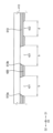
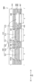
도 2에 도시된 바와 같이, 표시 장치(100)는 표시 영역(10) 및 주변 영역(20)을 포함할 수 있다. 여기서, 표시 영역(10)은 복수의 화소 영역들(30)을 포함할 수 있다. 복수의 화소 영역들(30)은 매트릭스 형태로 표시 영역(10)에 전체적으로 배열될 수 있다. 화소 영역들(30) 각각은 제1 서브 화소 영역(31), 제2 서브 화소 영역(32) 및 제3 서브 화소 영역(33)을 포함할 수 있다. As illustrated in FIG. 2, the display device (100) may include a display area (10) and a peripheral area (20). Here, the display area (10) may include a plurality of pixel areas (30). The plurality of pixel areas (30) may be arranged in the entire display area (10) in a matrix form. Each of the pixel areas (30) may include a first sub-pixel area (31), a second sub-pixel area (32), and a third sub-pixel area (33).
예시적인 실시예들에 있어서, 표시 장치(100)의 상면과 평행한 제1 방향(D1)을 따라 제2 서브 화소 영역(32), 제3 서브 화소 영역(33) 및 제1 서브 화소 영역(31)이 순서대로 배열될 수 있고, 제2 서브 화소 영역(32) 및 제3 서브 화소 영역(33) 각각의 크기보다 제1 서브 화소 영역(31)의 크기가 상대적으로 더 작을 수 있다.In exemplary embodiments, a second sub-pixel region (32), a third sub-pixel region (33), and a first sub-pixel region (31) may be arranged in sequence along a first direction (D1) parallel to an upper surface of a display device (100), and a size of the first sub-pixel region (31) may be relatively smaller than each of the sizes of the second sub-pixel region (32) and the third sub-pixel region (33).
예를 들면, 표시 영역(10)에는 화소 구조물들(예를 들어, 반도체 소자, 발광 구조물 등)이 배치될 수 있고, 주변 영역(20)에는 상기 실링 부재, 신호 배선들, 전원 배선들 등이 배치될 수 있다.For example, pixel structures (e.g., semiconductor elements, light-emitting structures, etc.) may be arranged in the display area (10), and sealing members, signal wires, power wires, etc. may be arranged in the peripheral area (20).
다만, 본 발명에 있어서, 화소 영역들(30) 각각에 포함된 제2 서브 화소 영역(32), 제3 서브 화소 영역(33) 및 제1 서브 화소 영역(31)의 배열이 제1 방향(D1)을 따라 배열되는 것으로 설명하였지만, 본 발명의 구성이 이에 한정되는 것은 아니다. 예를 들면, 제1 서브 화소 영역(31)이 제2 서브 화소 영역(32)으로부터 제1 방향(D1)과 반대되는 제2 방향(D2)으로 이격하여 위치할 수도 있다. 이와는 달리, 제1 서브 화소 영역(31)이 제2 서브 화소 영역(32) 및 제3 서브 화소 영역(33)으로부터 제1 방향(D1) 및 제2 방향(D2)과 직교하는 제3 방향(D3) 또는 제3 방향(D3)에 반대되는 제4 방향(D4)으로 이격하여 위치할 수도 있다.However, in the present invention, the arrangement of the second sub-pixel area (32), the third sub-pixel area (33), and the first sub-pixel area (31) included in each of the pixel areas (30) has been described as being arranged along the first direction (D1), but the configuration of the present invention is not limited thereto. For example, the first sub-pixel area (31) may be positioned spaced apart from the second sub-pixel area (32) in a second direction (D2) opposite to the first direction (D1). Alternatively, the first sub-pixel area (31) may be positioned spaced apart from the second sub-pixel area (32) and the third sub-pixel area (33) in a third direction (D3) orthogonal to the first direction (D1) and the second direction (D2) or in a fourth direction (D4) opposite to the third direction (D3).
또한, 본 발명에 있어서, 제2 서브 화소 영역(32)의 크기와 제3 서브 화소 영역(33)의 크기가 동일한 것으로 도시되어 있으나, 본 발명의 구성이 이에 한정되는 것은 아니다. 예를 들면, 제2 서브 화소 영역(32)의 크기가 제3 서브 화소 영역(33)의 크기보다 크거나 작을 수도 있다. 다만, 제2 서브 화소 영역(32)의 크기가 제3 서브 화소 영역(33)의 크기보다 작더라도, 제2 서브 화소 영역(32)의 크기는 제1 서브 화소 영역(31)보다 클 수 있다.In addition, in the present invention, the size of the second sub-pixel area (32) and the size of the third sub-pixel area (33) are illustrated as being the same, but the configuration of the present invention is not limited thereto. For example, the size of the second sub-pixel area (32) may be larger or smaller than the size of the third sub-pixel area (33). However, even if the size of the second sub-pixel area (32) is smaller than the size of the third sub-pixel area (33), the size of the second sub-pixel area (32) may be larger than the first sub-pixel area (31).
또한, 본 발명의 화소 영역(30)이 3개의 서브 화소 영역들(31, 32, 33)을 포함하는 것으로 설명하였으나, 본 발명의 구성이 이에 한정되는 것은 아니다. 예를 들면, 화소 영역(30)은 2개의 서브 화소 영역들 또는 적어도 4개의 서브 화소 영역들을 포함할 수도 있다.In addition, although the pixel area (30) of the present invention is described as including three sub-pixel areas (31, 32, 33), the configuration of the present invention is not limited thereto. For example, the pixel area (30) may include two sub-pixel areas or at least four sub-pixel areas.
더욱이, 본 발명의 표시 영역(10), 주변 영역(20), 화소 영역(30), 제1 서브 화소 영역(31), 제2 서브 화소 영역(32) 및 제3 서브 화소 영역(33) 각각의 형상이 사각형의 평면 형상을 갖는 것으로 설명하였지만, 본 발명의 구성이 이에 한정되는 것은 아니다. 예를 들면, 상기 형상은 삼각형의 평면 형상, 마름모의 평면 형상, 다각형의 평면 형상, 원형의 평면 형상, 트랙형의 평면 형상 또는 타원형의 평면 형상을 가질 수도 있다.Furthermore, although the shapes of the display area (10), the peripheral area (20), the pixel area (30), the first sub-pixel area (31), the second sub-pixel area (32), and the third sub-pixel area (33) of the present invention have been described as having a rectangular planar shape, the configuration of the present invention is not limited thereto. For example, the shape may have a triangular planar shape, a rhombus planar shape, a polygonal planar shape, a circular planar shape, a track-shaped planar shape, or an elliptical planar shape.
도 3에 도시된 바와 같이, 하부 구조물(500)은 하부 기판(110), 화소 정의막(310) 등을 포함할 수 있다. 하부 기판(110) 상에 화소 정의막(310)이 배치될 수 있다. 화소 정의막(310)은 화소 개구들(311) 및 소형 화소 개구들(312)을 포함할 수 있다. 예를 들면, 화소 개구들(311)은 제2 서브 화소 영역(32) 및 제3 서브 화소 영역(33) 각각과 대응될 수 있고, 소형 화소 개구들(312)은 제1 서브 화소 영역(31)과 대응될 수 있다. 다시 말하면, 화소 개구들(311) 각각의 크기는 제2 서브 화소 영역(32) 및 제3 서브 화소 영역(33) 각각의 크기와 실질적으로 동일할 수 있고, 소형 화소 개구들(312) 각각의 크기는 제1 서브 화소 영역(31)의 크기와 실질적으로 동일할 수 있다.As illustrated in FIG. 3, the lower structure (500) may include a lower substrate (110), a pixel defining film (310), etc. The pixel defining film (310) may be disposed on the lower substrate (110). The pixel defining film (310) may include pixel openings (311) and small pixel openings (312). For example, the pixel openings (311) may correspond to each of the second sub-pixel region (32) and the third sub-pixel region (33), and the small pixel openings (312) may correspond to the first sub-pixel region (31). In other words, the size of each of the pixel openings (311) may be substantially the same as the size of each of the second sub-pixel region (32) and the third sub-pixel region (33), and the size of each of the small pixel openings (312) may be substantially the same as the size of the first sub-pixel region (31).
도 4에 도시된 바와 같이, 상부 구조물(600)은 상부 기판(410), 차광 부재(420) 등을 포함할 수 있다. 상부 기판(410)의 저면 상에 차광 부재(420)가 배치될 수 있다. 예시적인 실시예들에 있어서, 차광 부재(420)는 개구들(421) 및 소형 개구들(422)을 포함할 수 있다. 예를 들면, 화소 개구들(311) 상에 개구들(421)이 각기 위치할 수 있고, 소형 화소 개구들(312) 상에 소형 개구들(422)이 각기 위치할 수 있다. 또한, 개구들(421) 각각의 크기는 화소 개구들(311) 각각의 크기보다 클 수 있고, 소형 개구들(422) 각각의 크기는 소형 화소 개구들(312) 각각의 크기보다 클 수 있다.As illustrated in FIG. 4, the upper structure (600) may include an upper substrate (410), a light-shielding member (420), and the like. The light-shielding member (420) may be disposed on a lower surface of the upper substrate (410). In exemplary embodiments, the light-shielding member (420) may include openings (421) and small openings (422). For example, the openings (421) may be respectively positioned on the pixel openings (311), and the small openings (422) may be respectively positioned on the small pixel openings (312). In addition, the size of each of the openings (421) may be larger than the size of each of the pixel openings (311), and the size of each of the small openings (422) may be larger than the size of each of the small pixel openings (312).
예를 들면, 화소 정의막(310)의 화소 개구들(311) 및 소형 화소 개구들(312)에 발광층이 배치될 수 있고, 상기 발광층으로부터 방출된 광이 차광 부재(420)의 개구들(421) 및 소형 개구들(422)을 통해 외부로 방출될 수 있다.For example, a light-emitting layer may be arranged in the pixel apertures (311) and small pixel apertures (312) of the pixel defining film (310), and light emitted from the light-emitting layer may be emitted to the outside through the apertures (421) and small apertures (422) of the light-blocking member (420).
도 5는 도 1의 표시 장치에 포함된 화소 정의막의 개구 및 차광 부재의 개구가 중첩된 형상을 나타내는 평면도이고, 도 6은 도 5의 'A'영역을 확대 도시한 부분 확대 평면도이다. 도 7은 도 6의 화소 정의막의 개구 및 차광 부재의 개구가 중첩된 형상을 설명하기 위한 평면도이다.FIG. 5 is a plan view showing a shape in which an aperture of a pixel defining film and an aperture of a light blocking member included in the display device of FIG. 1 overlap, and FIG. 6 is a partial enlarged plan view showing an enlarged portion of area 'A' of FIG. 5. FIG. 7 is a plan view explaining a shape in which an aperture of a pixel defining film and an aperture of a light blocking member of FIG. 6 overlap.
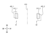
도 5, 6 및 7을 참조하면, 상부 기판(410)의 상면에 수직한 방향에서 볼 때, 화소 개구들(311)과 개구들(421)이 각기 중첩하여 위치할 수 있다. 다시 말하면, 개구들(421) 각각은 화소 개구들(311) 각각을 완전히 커버할 수 있다. 또한, 상부 기판(410)의 상면에 수직한 방향에서 볼 때, 소형 화소 개구들(312) 각각과 소형 개구들(422) 각각이 부분적으로 중첩할 수 있다. 다시 말하면, 소형 화소 개구들(312) 각각은 소형 개구들(422) 각각을 부분적으로 커버할 수 있다. 예시적인 실시예들에 있어서, 소형 개구들(422) 중 일부는 소형 화소 개구(312) 상에서 제1 방향(D1)으로 시프트되어 상기 소형 화소 개구(312)의 좌측부와 중첩하지 않을 수 있고, 소형 개구들(422) 중 나머지는 소형 화소 개구(312) 상에서 제2 방향(D2)으로 시프트되어 소형 화소 개구(312)의 우측부와 중첩하지 않을 수 있다.Referring to FIGS. 5, 6, and 7, when viewed in a direction perpendicular to the upper surface of the upper substrate (410), the pixel apertures (311) and the apertures (421) may be positioned to overlap each other. In other words, each of the apertures (421) may completely cover each of the pixel apertures (311). In addition, when viewed in a direction perpendicular to the upper surface of the upper substrate (410), each of the small pixel apertures (312) and each of the small apertures (422) may partially overlap each other. In other words, each of the small pixel apertures (312) may partially cover each of the small apertures (422). In exemplary embodiments, some of the small apertures (422) may be shifted in a first direction (D1) on the small pixel aperture (312) so as not to overlap with a left portion of the small pixel aperture (312), and the remainder of the small apertures (422) may be shifted in a second direction (D2) on the small pixel aperture (312) so as not to overlap with a right portion of the small pixel aperture (312).
예를 들면, 도 6에는 도시된 바와 같이, 화소 개구들(311)은 제1 화소 개구(311_1)(예를 들어, 제5 개구), 제2 화소 개구(311_2), 제3 화소 개구(311_3)(예를 들어, 제6 개구) 및 제4 화소 개구(311_4)를 포함할 수 있고, 소형 화소 개구들(312)은 제1 소형 화소 개구(312_1)(예를 들어, 제1 개구) 및 제2 소형 화소 개구(312_2)(예를 들어, 제2 개구)를 포함할 수 있다. 또한, 개구들(421)은 제1 개구(421_1)(예를 들어, 제7 개구), 제2 개구(421_2), 제3 개구(421_3)(예를 들어, 제8 개구) 및 제4 개구(421_4)를 포함할 수 있고, 소형 개구들(422)은 제1 소형 개구(422_1)(예를 들어, 제3 개구) 및 제2 소형 개구(422_2)(예를 들어, 제4 개구)를 포함할 수 있다.For example, as illustrated in FIG. 6, the pixel apertures (311) may include a first pixel aperture (311_1) (e.g., the fifth aperture), a second pixel aperture (311_2), a third pixel aperture (311_3) (e.g., the sixth aperture), and a fourth pixel aperture (311_4), and the small pixel apertures (312) may include a first small pixel aperture (312_1) (e.g., the first aperture) and a second small pixel aperture (312_2) (e.g., the second aperture). Additionally, the openings (421) may include a first opening (421_1) (e.g., the seventh opening), a second opening (421_2), a third opening (421_3) (e.g., the eighth opening), and a fourth opening (421_4), and the small openings (422) may include a first small opening (422_1) (e.g., the third opening) and a second small opening (422_2) (e.g., the fourth opening).
제1 화소 개구(311_1), 제2 화소 개구(311_2) 및 제1 소형 화소 개구(312_1)가 제1 화소 영역에 대응될 수 있고, 제3 화소 개구(311_3), 제4 화소 개구(311_4) 및 제2 소형 화소 개구(312_2)가 상기 제1 화소 영역과 인접하여 위치하는 제2 화소 영역에 대응될 수 있다. The first pixel opening (311_1), the second pixel opening (311_2), and the first small pixel opening (312_1) may correspond to the first pixel area, and the third pixel opening (311_3), the fourth pixel opening (311_4), and the second small pixel opening (312_2) may correspond to the second pixel area positioned adjacent to the first pixel area.
예시적인 실시예들에 있어서, 제1 소형 화소 개구(312_1)에 배치되는 발광층으로부터 방출된 광과 제2 소형 화소 개구(312_2)에 배치되는 발광층으로부터 방출되는 광은 동일한 색을 가지거나, 제1 소형 화소 개구(312_1)에 배치되는 발광층으로부터 방출된 광이 제1 소형 개구(422_1)를 통해 표시 장치(100)의 외부로 방출된 광의 색과 제2 소형 화소 개구(312_2)에 배치되는 발광층으로부터 방출된 광이 제2 소형 개구(422_2)를 통해 표시 장치(100)의 외부로 방출된 광의 색은 동일할 수 있다.In exemplary embodiments, light emitted from a light-emitting layer disposed in a first small pixel opening (312_1) and light emitted from a light-emitting layer disposed in a second small pixel opening (312_2) may have the same color, or the color of light emitted from a light-emitting layer disposed in a first small pixel opening (312_1) and emitted to the outside of the display device (100) through the first small opening (422_1) and the color of light emitted from a light-emitting layer disposed in a second small pixel opening (312_2) and emitted to the outside of the display device (100) through the second small opening (422_2) may be the same.
또한, 제1 화소 개구(311_1)에 배치되는 발광층으로부터 방출된 광과 제3 화소 개구(311_3)에 배치되는 발광층으로부터 방출되는 광은 동일한 색을 가지거나, 제1 화소 개구(311_1)에 배치되는 발광층으로부터 방출된 광이 제1 개구(421_1)를 통해 표시 장치(100)의 외부로 방출된 광의 색과 제3 화소 개구(311_3)에 배치되는 발광층으로부터 방출된 광이 제3 개구(421_3)를 통해 표시 장치(100)의 외부로 방출된 광의 색은 동일할 수 있다.In addition, the light emitted from the light emitting layer disposed in the first pixel opening (311_1) and the light emitted from the light emitting layer disposed in the third pixel opening (311_3) may have the same color, or the color of the light emitted from the light emitting layer disposed in the first pixel opening (311_1) and emitted to the outside of the display device (100) through the first opening (421_1) and the color of the light emitted from the light emitting layer disposed in the third pixel opening (311_3) and emitted to the outside of the display device (100) through the third opening (421_3) may be the same.
더욱이, 제2 화소 개구(311_2)에 배치되는 발광층으로부터 방출된 광과 제4 화소 개구(311_4)에 배치되는 발광층으로부터 방출되는 광은 동일한 색을 가지거나, 제2 화소 개구(311_2)에 배치되는 발광층으로부터 방출된 광이 제2 개구(421_2)를 통해 표시 장치(100)의 외부로 방출된 광의 색과 제4 화소 개구(311_4)에 배치되는 발광층으로부터 방출된 광이 제4 개구(421_4)를 통해 표시 장치(100)의 외부로 방출된 광의 색은 동일할 수 있다.Furthermore, the light emitted from the light emitting layer disposed in the second pixel opening (311_2) and the light emitted from the light emitting layer disposed in the fourth pixel opening (311_4) may have the same color, or the color of the light emitted from the light emitting layer disposed in the second pixel opening (311_2) and emitted to the outside of the display device (100) through the second opening (421_2) and the color of the light emitted from the light emitting layer disposed in the fourth pixel opening (311_4) and emitted to the outside of the display device (100) through the fourth opening (421_4) may be the same.
제1 화소 개구(311_1), 제2 화소 개구(311_2), 제3 화소 개구(311_3) 및 제4 화소 개구(311_4) 각각의 폭은 제1 폭(a)을 가질 수 있고, 제1 개구(421_1), 제2 개구(421_2), 제3 개구(421_3) 및 제4 개구(421_4) 각각의 폭은 제2 폭(b)을 가질 수 있다. 여기서, 제1 폭(a)은 제2 폭(b)보다 작을 수 있다. 또한, 제1 소형 화소 개구(312_1) 및 제2 소형 화소 개구(312_2) 각각의 폭은 제3 폭(c)을 가질 수 있고, 제1 소형 개구(422_1) 및 제2 소형 개구(422_2) 각각의 폭은 제4 폭(d)을 가질 수 있다. 여기서, 제3 폭(c)은 제4 폭(d)보다 작을 수 있다.Each of the first pixel aperture (311_1), the second pixel aperture (311_2), the third pixel aperture (311_3), and the fourth pixel aperture (311_4) may have a first width (a), and each of the first aperture (421_1), the second aperture (421_2), the third aperture (421_3), and the fourth aperture (421_4) may have a second width (b). Here, the first width (a) may be smaller than the second width (b). In addition, each of the first small pixel aperture (312_1) and the second small pixel aperture (312_2) may have a third width (c), and each of the first small aperture (422_1) and the second small aperture (422_2) may have a fourth width (d). Here, the third width (c) may be smaller than the fourth width (d).
제1 개구(421_1), 제2 개구(421_2), 제3 개구(421_3) 및 제4 개구(421_4)는 제1 화소 개구(311_1), 제2 화소 개구(311_2), 제3 화소 개구(311_3) 및 제4 화소 개구(311_4)와 각기 중첩할 수 있다. 다시 말하면, 제1 개구(421_1), 제2 개구(421_2), 제3 개구(421_3) 및 제4 개구(421_4)는 제1 화소 개구(311_1), 제2 화소 개구(311_2), 제3 화소 개구(311_3) 및 제4 화소 개구(311_4)를 각기 완전히 커버할 수 있다. 즉, 제1 개구(421_1), 제2 개구(421_2), 제3 개구(421_3) 및 제4 개구(421_4) 각각의 크기는 제1 화소 개구(311_1), 제2 화소 개구(311_2), 제3 화소 개구(311_3) 및 제4 화소 개구(311_4) 각각의 크기보다 클 수 있다.The first aperture (421_1), the second aperture (421_2), the third aperture (421_3), and the fourth aperture (421_4) can overlap the first pixel aperture (311_1), the second pixel aperture (311_2), the third pixel aperture (311_3), and the fourth pixel aperture (311_4), respectively. In other words, the first aperture (421_1), the second aperture (421_2), the third pixel aperture (311_3), and the fourth aperture (421_4) can completely cover the first pixel aperture (311_1), the second pixel aperture (311_2), the third pixel aperture (311_3), and the fourth pixel aperture (311_4), respectively. That is, the size of each of the first aperture (421_1), the second aperture (421_2), the third aperture (421_3), and the fourth aperture (421_4) may be larger than the size of each of the first pixel aperture (311_1), the second pixel aperture (311_2), the third pixel aperture (311_3), and the fourth pixel aperture (311_4).
이와는 달리, 제1 소형 개구(422_1) 및 제2 소형 개구(422_2)는 제1 소형 화소 개구(312_1)및 제2 소형 화소 개구(312_2)와 각기 부분적으로 중첩할 수 있다. 다시 말하면, 제1 소형 개구(422_1) 및 제2 소형 개구(422_2)는 제1 소형 화소 개구(312_1)및 제2 소형 화소 개구(312_2)를 각기 부분적으로 커버할 수 있다.In contrast, the first small aperture (422_1) and the second small aperture (422_2) may partially overlap the first small pixel aperture (312_1) and the second small pixel aperture (312_2), respectively. In other words, the first small aperture (422_1) and the second small aperture (422_2) may partially cover the first small pixel aperture (312_1) and the second small pixel aperture (312_2), respectively.
예시적인 실시예들에 있어서, 제1 소형 화소 개구(312_1)로부터 제2 소형 화소 개구(312_2)가 제1 방향(D1)으로 이격되어 위치할 수 있고, 제1 소형 개구(422_1)로부터 제2 소형 개구(422_2)가 제1 방향(D1)으로 이격되어 위치할 수 있다. In exemplary embodiments, the second small pixel aperture (312_2) may be positioned spaced apart from the first small pixel aperture (312_1) in the first direction (D1), and the second small aperture (422_2) may be positioned spaced apart from the first small pixel aperture (422_1) in the first direction (D1).
또한, 제1 소형 화소 개구(312_1) 및 제2 소형 화소 개구(312_2) 각각의 좌측부를 제1 부분 및 우측부를 제2 부분으로 정의한다. 제1 소형 개구(422_1)는 제1 소형 화소 개구(312_1) 상에서 제1 방향(D1)으로 시프트되어 제1 소형 화소 개구(312_1)의 제1 부분과 중첩하지 않을 수 있고, 제2 소형 개구(422_2)는 제2 소형 화소 개구(312_2) 상에서 제2 방향(D2)으로 시프트되어 제2 소형 화소 개구(312_2)의 제2 부분과 중첩하지 않을 수 있다.In addition, the left part of each of the first small pixel opening (312_1) and the second small pixel opening (312_2) is defined as the first part, and the right part is defined as the second part. The first small opening (422_1) may be shifted in the first direction (D1) on the first small pixel opening (312_1) so as not to overlap with the first part of the first small pixel opening (312_1), and the second small opening (422_2) may be shifted in the second direction (D2) on the second small pixel opening (312_2) so as not to overlap with the second part of the second small pixel opening (312_2).
예시적인 실시예들에 있어서, 도 7에 도시된 바와 같이, 상부 기판(410)의 상면에 수직한 방향에서 볼 때, 제1 소형 화소 개구(312_1)와 제1 소형 개구(422_1)가 중첩된 제1 형상(S1)과 제2 소형 화소 개구(312_2)와 제2 소형 개구(422_2)가 중첩된 제2 형상(S2)은 가상선(610)에 대하여 서로 대칭일 수 있다. 여기서, 가상선(610)은 제1 형상(S1)과 제2 형상(S2) 사이의 중간 지점에 위치하고, 제1 방향(D1) 및 제2 방향(D2)에 수직한 제3 방향(D3)(또는 제4 방향(D4))으로 연장할 수 있다. 한편, 도 8에 도시된 바와 같이, 화소 정의막(310)과 하부 기판(110) 사이에는 하부 전극들이 배치될 수 있고, 제1 소형 화소 개구(312_1)와 중첩하는 하부 전극을 제1 하부 전극 및 제2 소형 화소 개구(312_2)와 중첩하는 하부 전극을 제2 하부 전극으로 정의한다. 제1 소형 화소 개구(312_1)는 제1 하부 전극의 상면의 일부를 노출시킬 수 있고, 제2 소형 화소 개구(312_2)는 제2 하부 전극의 상면의 일부를 노출시킬 수 있다. 다시 말하면, 화소 정의막(310)이 상기 제1 및 제2 하부 전극들 각각의 외곽부를 커버할 수 있고, 상기 제1 및 제2 하부 전극들 각각은 사각형의 평면 형상을 가질 수 있다. 상기 제1 및 제2 하부 전극들 각각은 제1 부분 및 상기 제1 부분과 마주보는 제2 부분을 포함하고, 차광 부재(420)는 상기 제1 하부 전극의 상기 제1 부분 및 상기 제2 하부 전극의 제2 부분과 중첩할 수 있다. 예를 들면, 제1 소형 개구(422_1)가 제1 방향(D1)으로 시프트되어 형성됨으로써 상기 제1 하부 전극의 좌측부가 차광 부재(420)와 중첩할 수 있고, 제2 소형 개구(422_2)가 제2 방향(D2)으로 시프트되어 형성됨으로써 상기 제2 하부 전극의 우측부가 차광 부재(420)와 중첩할 수 있다.In exemplary embodiments, as illustrated in FIG. 7, when viewed in a direction perpendicular to the upper surface of the upper substrate (410), a first shape (S1) in which a first small pixel opening (312_1) and a first small opening (422_1) overlap and a second shape (S2) in which a second small pixel opening (312_2) and a second small opening (422_2) overlap may be symmetrical with respect to a virtual line (610). Here, the virtual line (610) is located at a midpoint between the first shape (S1) and the second shape (S2), and may extend in a third direction (D3) (or a fourth direction (D4)) perpendicular to the first direction (D1) and the second direction (D2). Meanwhile, as illustrated in FIG. 8, lower electrodes may be arranged between the pixel defining film (310) and the lower substrate (110), and the lower electrode overlapping the first small pixel opening (312_1) is defined as the first lower electrode, and the lower electrode overlapping the second small pixel opening (312_2) is defined as the second lower electrode. The first small pixel opening (312_1) may expose a part of the upper surface of the first lower electrode, and the second small pixel opening (312_2) may expose a part of the upper surface of the second lower electrode. In other words, the pixel defining film (310) may cover an outer portion of each of the first and second lower electrodes, and each of the first and second lower electrodes may have a rectangular planar shape. Each of the first and second lower electrodes includes a first portion and a second portion facing the first portion, and the light blocking member (420) can overlap the first portion of the first lower electrode and the second portion of the second lower electrode. For example, the first small opening (422_1) can be formed by being shifted in the first direction (D1) so that the left portion of the first lower electrode can overlap the light blocking member (420), and the second small opening (422_2) can be formed by being shifted in the second direction (D2) so that the right portion of the second lower electrode can overlap the light blocking member (420).
예를 들면, 종래의 표시 장치에 있어서, 수명, 구동 전류량, 제조 특성 등을 고려하여 특정 광(예를 들어, 청색광)이 방출되는 제1 서브 화소 영역의 크기(예를 들어, 화소 정의막의 제1 개구)를 작게 형성하는 경우가 있다. 따라서, 다른 광(예를 들어, 적색광 또는 녹색광)이 방출되는 제2 서브 화소 영역(예를 들어, 화소 정의막의 제2 개구)의 크기는 상대적으로 클 수 있다. 차광 부재를 포함하는 상부 구조물과 화소 정의막을 포함하는 하부 구조물을 결합 시 얼라인 틀어짐이 발생하는 경우, 상기 차광 부재의 차단부(예를 들어, 인접한 개구들 사이)가 상기 제1 및 제2 서브 화소 영역들 각각과 중첩할 수 있다 이러한 경우, 상기 제2 서브 화소 영역에 비해 상기 특정 광이 방출되는 상기 제1 서브 화소 영역은 상대적으로 크기가 작기 때문에 외부로 방출되는 상기 특정 광의 휘도 변화량이 상대적으로 클 수 있다. 다시 말하면, 상기 상부 구조물과 상기 하부 구조물이 정확하게 결합되는 것은 실질적으로 불가능하기 때문에, 결함 마진 범위 내에서 상기 상부 구조물과 상기 하부 구조물이 결합되어 있다. 다만, 상기 종래의 표시 장치의 해상도가 증가됨에 따라 상기 제1 서브 화소 영역은 더욱 작아지고, 얼라인 틀어짐에 따른 종래의 표시 장치의 불량이 더욱 야기되고 있다.For example, in a conventional display device, in consideration of the lifespan, driving current, manufacturing characteristics, etc., there are cases where the size of a first sub-pixel region (e.g., a first opening of a pixel defining film) from which specific light (e.g., blue light) is emitted is formed small. Accordingly, the size of a second sub-pixel region (e.g., a second opening of a pixel defining film) from which other light (e.g., red light or green light) is emitted can be relatively large. When an upper structure including a light-blocking member and a lower structure including a pixel defining film are combined, if an alignment misalignment occurs, a blocking portion (e.g., between adjacent openings) of the light-blocking member can overlap each of the first and second sub-pixel regions. In this case, since the first sub-pixel region from which the specific light is emitted is relatively smaller than the second sub-pixel region, the luminance change amount of the specific light emitted to the outside can be relatively large. In other words, since it is practically impossible for the upper structure and the lower structure to be precisely combined, the upper structure and the lower structure are combined within a defect margin range. However, as the resolution of the conventional display device increases, the first sub-pixel area becomes smaller, and defects in the conventional display device due to misalignment are further caused.
예시적인 실시예들에 있어서, 표시 장치(100)는 제1 소형 화소 개구(312_1) 및 제2 소형 화소 개구(312_2) 각각과 부분적으로 중첩하는 제1 소형 개구(422_1) 및 제2 소형 개구(422_2)를 포함할 수 있다. 또한, 상부 기판(410)의 상면에 수직한 방향에서 볼 때, 제1 소형 화소 개구(312_1)와 제1 소형 개구(422_1)가 중첩된 제1 형상(S1)과 제2 소형 화소 개구(312_2)와 제2 소형 개구(422_2)가 중첩된 제2 형상(S2)은 가상선(610)에 대하여 서로 대칭일 수 있다. 따라서, 하부 구조물(500)과 상부 구조물(600)을 결합 시 얼라인 틀어짐이 발생하더라도, 제1 소형 개구(422_1) 및 제2 소형 개구(422_2)를 통해 외부로 방출되는 광의 총량이 일정할 수 있다. In exemplary embodiments, the display device (100) may include a first small opening (422_1) and a second small opening (422_2) that partially overlap the first small pixel opening (312_1) and the second small pixel opening (312_2), respectively. In addition, when viewed in a direction perpendicular to an upper surface of the upper substrate (410), a first shape (S1) in which the first small pixel opening (312_1) and the first small opening (422_1) overlap and a second shape (S2) in which the second small pixel opening (312_2) and the second small opening (422_2) overlap may be symmetrical with respect to a virtual line (610). Accordingly, even if misalignment occurs when combining the lower structure (500) and the upper structure (600), the total amount of light emitted to the outside through the first small opening (422_1) and the second small opening (422_2) can be constant.
예를 들면, 상부 구조물(600)이 제2 방향(D2)으로 시프트되는 얼라인 틀어짐이 발생할 경우, 제1 소형 화소 개구(312_1)와 제1 소형 개구(422_1)의 중첩되는 면적은 증가할 수 있고, 제2 소형 화소 개구(312_2)와 제2 소형 개구(422_2)의 중첩되는 면적은 감소할 수 있다. 이와는 달리, 상부 구조물(600)이 제1 방향(D1)으로 시프트되는 얼라인 틀어짐이 발생할 경우, 제1 소형 화소 개구(312_1)와 제1 소형 개구(422_1)의 중첩되는 면적은 감소할 수 있고, 제2 소형 화소 개구(312_2)와 제2 소형 개구(422_2)의 중첩되는 면적은 증가할 수 있다. 즉, 발광층으로부터 방출된 광이 제1 소형 개구(422_1) 및 제2 소형 개구(422_2)를 통해 표시 장치(100)의 외부로 방출될 경우, 상기 외부로 방출되는 광의 총량이 상기 얼라인 틀어짐의 발생에 관계없이 일정할 수 있다. 다시 말하면, 제1 소형 화소 개구(312_1) 및 제2 소형 화소 개구(312_2) 각각과 제1 소형 개구(422_1) 및 제2 소형 개구(422_2) 각각이 부분적으로 중첩함으로써, 상대적으로 상기 외부로 방출되는 광의 양이 기설정된 수준으로 조금 감소되지만, 상기 얼라인 틀어짐이 발생하더라도 상기 외부로 방출되는 광의 양은 상기 기설정된 수준으로 유지될 수 있다. 이에 따라, 본 발명의 예시적인 실시예들에 따른 표시 장치(100)는 상부 구조물(600)과 하부 구조물(500)의 결합 시 가로 방향(예를 들어, 제1 방향(D1) 또는 제2 방향(D2))으로의 얼라인 틀어짐에 대한 불량률을 감소시킬 수 있다.For example, when an alignment misalignment occurs in which the upper structure (600) shifts in the second direction (D2), the overlapping area of the first small pixel opening (312_1) and the first small opening (422_1) may increase, and the overlapping area of the second small pixel opening (312_2) and the second small opening (422_2) may decrease. In contrast, when an alignment misalignment occurs in which the upper structure (600) shifts in the first direction (D1), the overlapping area of the first small pixel opening (312_1) and the first small opening (422_1) may decrease, and the overlapping area of the second small pixel opening (312_2) and the second small opening (422_2) may increase. That is, when light emitted from the light-emitting layer is emitted to the outside of the display device (100) through the first small opening (422_1) and the second small opening (422_2), the total amount of light emitted to the outside can be constant regardless of the occurrence of the alignment misalignment. In other words, since each of the first small pixel opening (312_1) and the second small pixel opening (312_2) and each of the first small opening (422_1) and the second small opening (422_2) partially overlap, the amount of light emitted to the outside is relatively slightly reduced to a preset level, but even if the alignment misalignment occurs, the amount of light emitted to the outside can be maintained at the preset level. Accordingly, the display device (100) according to exemplary embodiments of the present invention can reduce the defect rate for misalignment in the horizontal direction (e.g., the first direction (D1) or the second direction (D2)) when the upper structure (600) and the lower structure (500) are combined.
도 8은 도 6의 I-I'라인을 따라 절단한 단면도이다.Figure 8 is a cross-sectional view taken along line I-I' of Figure 6.
도 8, 11 및 14를 참조하면, 표시 장치(100)는 하부 구조물(500) 및 상부 구조물(600)을 포함할 수 있다. Referring to FIGS. 8, 11 and 14, the display device (100) may include a lower structure (500) and an upper structure (600).
하부 구조물(500)은 하부 기판(110), 제1 반도체 소자(250_1), 제2 반도체 소자(250_2), 제3 반도체 소자(250_3), 게이트 절연층(150), 층간 절연층(190), 평탄화층(270), 제1 하부 전극(290_1), 제2 하부 전극(290_2), 제3 하부 전극(290_3), 화소 정의막(310), 발광층(330), 상부 전극(340), 박막 봉지 구조물(450) 등을 포함할 수 있다. 여기서, 제1 하부 전극(290_1), 발광층(330) 및 상부 전극(340)을 제1 서브 화소 구조물로 정의하고, 제2 하부 전극(290_2), 발광층(330) 및 상부 전극(340)을 제2 서브 화소 구조물로 정의하며, 제3 하부 전극(290_3), 발광층(330) 및 상부 전극(340)을 제3 서브 화소 구조물로 정의한다. 제1 반도체 소자(250_1)는 제1 액티브층(130_1), 제1 게이트 전극(170_1), 제1 소스 전극(210_1) 및 제1 드레인 전극(230_1)을 포함할 수 있고, 제2 반도체 소자(250_2)는 제2 액티브층(130_2), 제2 게이트 전극(170_2),제2 소스 전극(210_2) 및 제2 드레인 전극(230_2)을 포함할 수 있으며, 제3 반도체 소자(250_3)는 제3 액티브층(130_3), 제3 게이트 전극(170_3), 제3 소스 전극(210_3) 및 제3 드레인 전극(230_3)을 포함할 수 있다. 또한, 박막 봉지 구조물(450)은 제1 무기 박막 봉지층(451), 유기 박막 봉지층(452) 및 제2 무기 박막 봉지층(453)을 포함할 수 있다. 예시적인 실시예들에 있어서, 화소 정의막(310)은 화소 개구들(311) 및 소형 화소 개구(312)를 포함할 수 있다.The lower structure (500) may include a lower substrate (110), a first semiconductor element (250_1), a second semiconductor element (250_2), a third semiconductor element (250_3), a gate insulating layer (150), an interlayer insulating layer (190), a planarizing layer (270), a first lower electrode (290_1), a second lower electrode (290_2), a third lower electrode (290_3), a pixel defining film (310), a light-emitting layer (330), an upper electrode (340), a thin film encapsulation structure (450), etc. Here, the first lower electrode (290_1), the light-emitting layer (330), and the upper electrode (340) are defined as the first sub-pixel structure, the second lower electrode (290_2), the light-emitting layer (330), and the upper electrode (340) are defined as the second sub-pixel structure, and the third lower electrode (290_3), the light-emitting layer (330), and the upper electrode (340) are defined as the third sub-pixel structure. The first semiconductor element (250_1) may include a first active layer (130_1), a first gate electrode (170_1), a first source electrode (210_1), and a first drain electrode (230_1), the second semiconductor element (250_2) may include a second active layer (130_2), a second gate electrode (170_2), a second source electrode (210_2), and a second drain electrode (230_2), and the third semiconductor element (250_3) may include a third active layer (130_3), a third gate electrode (170_3), a third source electrode (210_3), and a third drain electrode (230_3). In addition, the thin film encapsulation structure (450) may include a first inorganic thin film encapsulation layer (451), an organic thin film encapsulation layer (452), and a second inorganic thin film encapsulation layer (453). In exemplary embodiments, the pixel defining film (310) may include pixel apertures (311) and small pixel apertures (312).
상부 구조물(600)은 제1 보호 절연층(490), 제2 보호 절연층(495), 복수의 광학 필터들(530), 중간층(497), 복수의 컬러 필터들(510), 차광 부재(420), 차광막(430), 상부 기판(410) 등을 포함할 수 있다. 여기서, 광학 필터들(530)은 제1 양자점 패턴(531)(예를 들어, 제2 광학 필터), 산란 패턴(532)(예를 들어, 제1 광학 필터) 및 제2 양자점 패턴(533)을 포함할 수 있다. 더욱이, 컬러 필터들(510)은 제1 컬러 필터(513), 제2 컬러 필터(511) 및 제3 컬러 필터(512)를 포함할 수 있다. 예시적인 실시예들에 있어서, 차광 부재(420)는 개구들(421) 및 소형 개구(422)를 포함할 수 있다.The upper structure (600) may include a first protective insulating layer (490), a second protective insulating layer (495), a plurality of optical filters (530), an intermediate layer (497), a plurality of color filters (510), a light-shielding member (420), a light-shielding film (430), an upper substrate (410), etc. Here, the optical filters (530) may include a first quantum dot pattern (531) (e.g., a second optical filter), a scattering pattern (532) (e.g., a first optical filter), and a second quantum dot pattern (533). Furthermore, the color filters (510) may include a first color filter (513), a second color filter (511), and a third color filter (512). In exemplary embodiments, the light-shielding member (420) may include openings (421) and small openings (422).
도 2에 도시된 제2 서브 화소 영역(32)에 상기 제1 서브 화소 구조물이 배치될 수 있고, 제3 서브 화소 영역(33)에 상기 제2 서브 화소 구조물이 배치될 수 있으며, 제1 서브 화소 영역(31)에 상기 제3 서브 화소 구조물이 배치될 수 있다. 표시 장치(100)는 상기 제1 내지 제3 서브 화소 구조물들을 통해 화상을 표시할 수 있다. The first sub-pixel structure may be arranged in the second sub-pixel area (32) illustrated in FIG. 2, the second sub-pixel structure may be arranged in the third sub-pixel area (33), and the third sub-pixel structure may be arranged in the first sub-pixel area (31). The display device (100) may display an image through the first to third sub-pixel structures.
도 8을 다시 참조하면, 투명한 또는 불투명한 재료를 포함하는 하부 기판(110)이 제공될 수 있다. 하부 기판(110)은 석영(quartz) 기판, 합성 석영(synthetic quartz) 기판, 불화칼슘(calcium fluoride) 기판, 불소가 도핑된 석영(F-doped quartz) 기판, 소다라임(sodalime) 유리 기판, 무알칼리(non-alkali) 유리 기판 등을 포함할 수 있다.Referring again to FIG. 8, a lower substrate (110) comprising a transparent or opaque material may be provided. The lower substrate (110) may include a quartz substrate, a synthetic quartz substrate, a calcium fluoride substrate, a fluorine-doped quartz substrate, a sodalime glass substrate, a non-alkali glass substrate, and the like.
다른 예시적인 실시예들에 있어서, 하부 기판(110)은 연성을 갖는 투명 수지 기판으로 이루어질 수도 있다. 하부 기판(110)으로 이용될 수 있는 투명 수지 기판의 예로는 폴리이미드 기판을 들 수 있다. 이러한 경우, 상기 폴리이미드 기판은 제1 폴리이미드층, 베리어 필름층, 제2 폴리이미드층 등을 포함하는 적층 구조를 가질 수 있다.In other exemplary embodiments, the lower substrate (110) may be formed of a transparent resin substrate having flexibility. An example of a transparent resin substrate that can be used as the lower substrate (110) is a polyimide substrate. In this case, the polyimide substrate may have a laminated structure including a first polyimide layer, a barrier film layer, a second polyimide layer, and the like.
하부 기판(110) 상에 버퍼층이 배치될 수도 있다. 상기 버퍼층은 하부 기판(110) 상에 전체적으로 배치될 수 있다. 상기 버퍼층은 하부 기판(110)으로부터 금속 원자들이나 불순물들이 반도체 소자 및 상기 서브 화소 구조물로 확산되는 현상을 방지할 수 있으며, 액티브층을 형성하기 위한 결정화 공정 동안 열의 전달 속도를 조절하여 실질적으로 균일한 액티브층을 수득하게 할 수 있다. 또한, 상기 버퍼층은 하부 기판(110)의 표면이 균일하지 않을 경우, 하부 기판(110)의 표면의 평탄도를 향상시키는 역할을 수행할 수 있다. 하부 기판(110)의 유형에 따라 하부 기판(110) 상에 두 개 이상의 버퍼층이 제공될 수 있거나 상기 버퍼층이 배치되지 않을 수 있다. 예를 들면, 상기 버퍼층은 유기 물질 또는 무기 물질을 포함할 수 있다.A buffer layer may be disposed on the lower substrate (110). The buffer layer may be disposed entirely on the lower substrate (110). The buffer layer may prevent metal atoms or impurities from diffusing from the lower substrate (110) to the semiconductor element and the sub-pixel structure, and may control the heat transfer rate during the crystallization process for forming the active layer to obtain a substantially uniform active layer. In addition, the buffer layer may play a role in improving the flatness of the surface of the lower substrate (110) when the surface of the lower substrate (110) is not uniform. Depending on the type of the lower substrate (110), two or more buffer layers may be provided on the lower substrate (110), or the buffer layer may not be disposed. For example, the buffer layer may include an organic material or an inorganic material.
하부 기판(110) 상에 제1 내지 제3 액티브층들(130_1, 130_2, 130_3)이 서로 이격하여 배치될 수 있다. 제1 내지 제3 액티브층들(130_1, 130_2, 130_3) 각각은 금속 산화물 반도체, 무기물 반도체(예를 들면, 아몰퍼스 실리콘(amorphous silicon), 폴리 실리콘(poly silicon)) 또는 유기물 반도체 등을 포함할 수 있고, 소스 영역 및 드레인 영역을 포함할 수 있다.First to third active layers (130_1, 130_2, 130_3) may be arranged spaced apart from each other on the lower substrate (110). Each of the first to third active layers (130_1, 130_2, 130_3) may include a metal oxide semiconductor, an inorganic semiconductor (e.g., amorphous silicon, poly silicon), an organic semiconductor, etc., and may include a source region and a drain region.
제1 내지 제3 액티브층들(130_1, 130_2, 130_3) 상에는 게이트 절연층(150)이 배치될 수 있다. 게이트 절연층(150)은 하부 기판(110) 상에서 제1 내지 제3 액티브층들(130_1, 130_2, 130_3)을 덮을 수 있으며, 하부 기판(110) 상에 전체적으로 배치될 수 있다. 예를 들면, 게이트 절연층(150)은 하부 기판(110) 상에서 제1 내지 제3 액티브층들(130_1, 130_2, 130_3)을 충분히 덮을 수 있으며, 제1 내지 제3 액티브층들(130_1, 130_2, 130_3)의주위에 단차를 생성시키지 않고 실질적으로 평탄한 상면을 가질 수 있다. 선택적으로, 게이트 절연층(150)은 하부 기판(110) 상에서 제1 내지 제3 액티브층들(130_1, 130_2, 130_3)을 덮으며, 균일한 두께로 제1 내지 제3 액티브층들(130_1, 130_2, 130_3)의 프로파일을 따라 배치될 수도 있다. 게이트 절연층(150)은 실리콘 화합물, 금속 산화물 등을 포함할 수 있다. 예를 들면, 게이트 절연층(150)은 실리콘 산화물(SiO), 실리콘 질화물(SiN), 실리콘 산질화물(SiON), 실리콘 산탄화물(SiOC), 실리콘 탄질화물(SiCN), 알루미늄 산화물(AlO), 알루미늄 질화물(AlN), 탄탈륨 산화물(TaO), 하프늄 산화물(HfO), 지르코늄 산화물(ZrO), 티타늄 산화물(TiO) 등을 포함할 수 있다. 다른 예시적인 실시예들에 있어서, 게이트 절연층(150)은 복수의 절연층들을 포함하는 다층 구조를 가질 수도 있다. 예를 들면, 상기 절연층들은 두께가 서로 다르거나 서로 다른 물질을 포함할 수 있다.A gate insulating layer (150) may be disposed on the first to third active layers (130_1, 130_2, 130_3). The gate insulating layer (150) may cover the first to third active layers (130_1, 130_2, 130_3) on the lower substrate (110) and may be disposed entirely on the lower substrate (110). For example, the gate insulating layer (150) may sufficiently cover the first to third active layers (130_1, 130_2, 130_3) on the lower substrate (110) and may have a substantially flat upper surface without generating a step around the first to third active layers (130_1, 130_2, 130_3). Optionally, the gate insulating layer (150) may cover the first to third active layers (130_1, 130_2, 130_3) on the lower substrate (110) and may be arranged along the profiles of the first to third active layers (130_1, 130_2, 130_3) with a uniform thickness. The gate insulating layer (150) may include a silicon compound, a metal oxide, or the like. For example, the gate insulating layer (150) may include silicon oxide (SiO), silicon nitride (SiN), silicon oxynitride (SiON), silicon oxycarbide (SiOC), silicon carbonitride (SiCN), aluminum oxide (AlO), aluminum nitride (AlN), tantalum oxide (TaO), hafnium oxide (HfO), zirconium oxide (ZrO), titanium oxide (TiO), or the like. In other exemplary embodiments, the gate insulating layer (150) may have a multilayer structure including a plurality of insulating layers. For example, the insulating layers may have different thicknesses or contain different materials.
게이트 절연층(150) 상에 제1 내지 제3 게이트 전극들(170_1, 170_2, 170_3)이 서로 이격하여 배치될 수 있다. 예를 들면, 제1 게이트 전극(170_1)은 게이트 절연층(150) 중에서 하부에 제1 액티브층(130_1)이 위치하는 부분 상에 배치될 수 있고, 제2 게이트 전극(170_2)은 게이트 절연층(150) 중에서 하부에 제2 액티브층(130_2)이 위치하는 부분 상에 배치될 수 있으며, 제3 게이트 전극(170_3)은 게이트 절연층(150) 중에서 하부에 제3 액티브층(130_3)이 위치하는 부분 상에 배치될 수 있다. 제1 내지 제3 게이트 전극들(170_1, 170_2, 170_3) 각각은 금속, 합금, 금속 질화물, 도전성 금속 산화물, 투명 도전성 물질 등을 포함할 수 있다. 예를 들면, 제1 내지 제3 게이트 전극들(170_1, 170_2, 170_3) 각각은 금(Au), 은(Ag), 알루미늄(Al), 백금(Pt), 니켈(Ni), 티타늄(Ti), 팔라듐(Pd), 마그네슘(Mg), 칼슘(Ca), 리튬(Li), 크롬(Cr), 탄탈륨(Ta), 텅스텐(W), 구리(Cu), 몰리브데늄(Mo), 스칸듐(Sc), 네오디뮴(Nd), 이리듐(Ir), 알루미늄을 함유하는 합금, 알루미늄 질화물(AlN), 은을 함유하는 합금, 텅스텐 질화물(WN), 구리를 함유하는 합금, 몰리브데늄을 함유하는 합금, 티타늄 질화물(TiN), 크롬 질화물(CrN), 탄탈륨 질화물(TaN), 스트론튬 루테늄 산화물(SrRuO), 아연 산화물(ZnO), 인듐 주석 산화물(ITO), 주석 산화물(SnO), 인듐 산화물(InO), 갈륨 산화물(GaO), 인듐 아연 산화물(IZO) 등을 포함할 수 있다. 이들은 단독으로 또는 서로 조합되어 사용될 수 있다. 다른 예시적인 실시예들에 있어서, 제1 내지 제3 게이트 전극들(170_1, 170_2, 170_3) 각각은 복수의 금속층들을 포함하는 다층 구조를 가질 수도 있다. 예를 들면, 상기 금속층들은 두께가 서로 다르거나 서로 다른 물질을 포함할 수 있다.First to third gate electrodes (170_1, 170_2, 170_3) may be arranged spaced apart from each other on the gate insulating layer (150). For example, the first gate electrode (170_1) may be arranged on a portion of the gate insulating layer (150) where the first active layer (130_1) is positioned underneath, the second gate electrode (170_2) may be arranged on a portion of the gate insulating layer (150) where the second active layer (130_2) is positioned underneath, and the third gate electrode (170_3) may be arranged on a portion of the gate insulating layer (150) where the third active layer (130_3) is positioned underneath. Each of the first to third gate electrodes (170_1, 170_2, 170_3) may include a metal, an alloy, a metal nitride, a conductive metal oxide, a transparent conductive material, or the like. For example, each of the first to third gate electrodes (170_1, 170_2, 170_3) may be formed of gold (Au), silver (Ag), aluminum (Al), platinum (Pt), nickel (Ni), titanium (Ti), palladium (Pd), magnesium (Mg), calcium (Ca), lithium (Li), chromium (Cr), tantalum (Ta), tungsten (W), copper (Cu), molybdenum (Mo), scandium (Sc), neodymium (Nd), iridium (Ir), an alloy containing aluminum, aluminum nitride (AlN), an alloy containing silver, tungsten nitride (WN), an alloy containing copper, an alloy containing molybdenum, titanium nitride (TiN), chromium nitride (CrN), tantalum nitride (TaN), strontium ruthenium oxide (SrRuO), zinc oxide (ZnO), indium tin oxide (ITO), tin oxide (SnO), indium It may include oxide (InO), gallium oxide (GaO), indium zinc oxide (IZO), etc. These may be used alone or in combination with each other. In other exemplary embodiments, each of the first to third gate electrodes (170_1, 170_2, 170_3) may have a multilayer structure including a plurality of metal layers. For example, the metal layers may have different thicknesses or include different materials.
제1 내지 제3 게이트 전극들(170_1, 170_2, 170_3) 상에는 층간 절연층(190)이 배치될 수 있다. 층간 절연층(190)은 게이트 절연층(150) 상에서 제1 내지 제3 게이트 전극들(170_1, 170_2, 170_3)을 덮을 수 있으며, 게이트 절연층(150) 상에서 전체적으로 배치될 수 있다. 예를 들면, 층간 절연층(190)은 게이트 절연층(150) 상에서 제1 내지 제3 게이트 전극들(170_1, 170_2, 170_3)을 충분히 덮을 수 있으며, 제1 내지 제3 게이트 전극들(170_1, 170_2, 170_3)의 주위에 단차를 생성시키지 않고 실질적으로 평탄한 상면을 가질 수 있다. 선택적으로, 층간 절연층(190)은 게이트 절연층(150) 상에서 제1 내지 제3 게이트 전극들(170_1, 170_2, 170_3)을 덮으며, 균일한 두께로 제1 내지 제3 게이트 전극들(170_1, 170_2, 170_3)의 프로파일을 따라 배치될 수도 있다. 층간 절연층(190)은 실리콘 화합물, 금속 산화물 등을 포함할 수 있다. 다른 예시적인 실시예들에 있어서, 층간 절연층(190)은 복수의 절연층들을 포함하는 다층 구조를 가질 수도 있다. 예를 들면, 상기 절연층들은 두께가 서로 다르거나 서로 다른 물질을 포함할 수 있다.An interlayer insulating layer (190) may be disposed on the first to third gate electrodes (170_1, 170_2, 170_3). The interlayer insulating layer (190) may cover the first to third gate electrodes (170_1, 170_2, 170_3) on the gate insulating layer (150) and may be disposed entirely on the gate insulating layer (150). For example, the interlayer insulating layer (190) may sufficiently cover the first to third gate electrodes (170_1, 170_2, 170_3) on the gate insulating layer (150) and may have a substantially flat upper surface without generating a step around the first to third gate electrodes (170_1, 170_2, 170_3). Optionally, the interlayer insulating layer (190) may cover the first to third gate electrodes (170_1, 170_2, 170_3) on the gate insulating layer (150) and may be arranged along the profiles of the first to third gate electrodes (170_1, 170_2, 170_3) with a uniform thickness. The interlayer insulating layer (190) may include a silicon compound, a metal oxide, or the like. In other exemplary embodiments, the interlayer insulating layer (190) may have a multilayer structure including a plurality of insulating layers. For example, the insulating layers may have different thicknesses or include different materials.
층간 절연층(190) 상에는 제1 소스 전극(210_1), 제1 드레인 전극(230_1), 제2 소스 전극(210_2), 제2 드레인 전극(230_2), 제3 소스 전극(210_3) 및 제3 드레인 전극(230_3)이 서로 이격하여 배치될 수 있다. 예를 들면, 제1 소스 전극(210_1)은 게이트 절연층(150) 및 층간 절연층(190)의 제1 부분을 제거하여 형성된 콘택홀을 통해 제1 액티브층(130_1)의 상기 소스 영역에 접속될 수 있고, 제1 드레인 전극(230_1)은 게이트 절연층(150) 및 층간 절연층(190)의 제2 부분을 제거하여 형성된 콘택홀을 통해 제1 액티브층(130_1)의 상기 드레인 영역에 접속될 수 있다. 또한, 제2 소스 전극(210_2)은 게이트 절연층(150) 및 층간 절연층(190)의 제3 부분을 제거하여 형성된 콘택홀을 통해 제2 액티브층(130_2)의 상기 소스 영역에 접속될 수 있고, 제2 드레인 전극(230_2)은 게이트 절연층(150) 및 층간 절연층(190)의 제4 부분을 제거하여 형성된 콘택홀을 통해 제2 액티브층(130_2)의 상기 드레인 영역에 접속될 수 있다. 더욱이, 제3 소스 전극(210_3)은 게이트 절연층(150) 및 층간 절연층(190)의 제5 부분을 제거하여 형성된 콘택홀을 통해 제3 액티브층(130_3)의 상기 소스 영역에 접속될 수 있고, 제3 드레인 전극(230_3)은 게이트 절연층(150) 및 층간 절연층(190)의 제6 부분을 제거하여 형성된 콘택홀을 통해 제3 액티브층(130_3)의 상기 드레인 영역에 접속될 수 있다. 제1 내지 제3 소스 전극들(210_1, 210_2, 210_3) 및 제1 내지 제3 드레인 전극들(230_1, 230_2, 230_3) 각각은 금속, 합금, 금속 질화물, 도전성 금속 산화물, 투명 도전성 물질 등을 포함할 수 있다. 이들은 단독으로 또는 서로 조합되어 사용될 수 있다. 다른 예시적인 실시예들에 있어서, 제1 내지 제3 소스 전극들(210_1, 210_2, 210_3) 및 제1 내지 제3 드레인 전극들(230_1, 230_2, 230_3) 각각은 복수의 금속층들을 포함하는 다층 구조를 가질 수도 있다. 예를 들면, 상기 금속층들은 두께가 서로 다르거나 서로 다른 물질을 포함할 수 있다.On the interlayer insulating layer (190), a first source electrode (210_1), a first drain electrode (230_1), a second source electrode (210_2), a second drain electrode (230_2), a third source electrode (210_3), and a third drain electrode (230_3) may be arranged to be spaced apart from each other. For example, the first source electrode (210_1) may be connected to the source region of the first active layer (130_1) through a contact hole formed by removing a first portion of the gate insulating layer (150) and the interlayer insulating layer (190), and the first drain electrode (230_1) may be connected to the drain region of the first active layer (130_1) through a contact hole formed by removing a second portion of the gate insulating layer (150) and the interlayer insulating layer (190). In addition, the second source electrode (210_2) can be connected to the source region of the second active layer (130_2) through a contact hole formed by removing the third portion of the gate insulating layer (150) and the interlayer insulating layer (190), and the second drain electrode (230_2) can be connected to the drain region of the second active layer (130_2) through a contact hole formed by removing the fourth portion of the gate insulating layer (150) and the interlayer insulating layer (190). Furthermore, the third source electrode (210_3) can be connected to the source region of the third active layer (130_3) through a contact hole formed by removing the fifth portion of the gate insulating layer (150) and the interlayer insulating layer (190), and the third drain electrode (230_3) can be connected to the drain region of the third active layer (130_3) through a contact hole formed by removing the sixth portion of the gate insulating layer (150) and the interlayer insulating layer (190). Each of the first to third source electrodes (210_1, 210_2, 210_3) and the first to third drain electrodes (230_1, 230_2, 230_3) may include a metal, an alloy, a metal nitride, a conductive metal oxide, a transparent conductive material, or the like. These may be used alone or in combination with each other. In other exemplary embodiments, each of the first to third source electrodes (210_1, 210_2, 210_3) and the first to third drain electrodes (230_1, 230_2, 230_3) may have a multilayer structure including a plurality of metal layers. For example, the metal layers may have different thicknesses or include different materials.
이에 따라, 제1 액티브층(130_1), 제1 게이트 전극(170_1), 제1 소스 전극(210_1) 및 제1 드레인 전극(230_1)을 포함하는 제1 반도체 소자(250_1)가 배치될 수 있고, 제2 액티브층(130_2), 제2 게이트 전극(170_2), 제2 소스 전극(210_2) 및 제2 드레인 전극(230_2)을 포함하는 제2 반도체 소자(250_2)가 배치될 수 있으며, 제3 액티브층(130_3), 제3 게이트 전극(170_3), 제3 소스 전극(210_3) 및 제3 드레인 전극(230_3)을 포함하는 제3 반도체 소자(250_3)가 배치될 수 있다.Accordingly, a first semiconductor element (250_1) including a first active layer (130_1), a first gate electrode (170_1), a first source electrode (210_1), and a first drain electrode (230_1) can be arranged, a second semiconductor element (250_2) including a second active layer (130_2), a second gate electrode (170_2), a second source electrode (210_2), and a second drain electrode (230_2) can be arranged, and a third semiconductor element (250_3) including a third active layer (130_3), a third gate electrode (170_3), a third source electrode (210_3), and a third drain electrode (230_3) can be arranged.
다만, 표시 장치(100)가 3개의 트랜지스터들(예를 들어, 제1 내지 제3 반도체 소자들(250_1, 250_2, 250_3))을 포함하는 구성을 갖는 것으로 설명하였으나, 본 발명의 구성이 이에 한정되는 것은 아니다. 예를 들면, 표시 장치(100)는 복수의 트랜지스터들 및 복수의 커패시터들을 포함하는 구성을 가질 수도 있다.However, although the display device (100) has been described as having a configuration including three transistors (for example, first to third semiconductor elements (250_1, 250_2, 250_3)), the configuration of the present invention is not limited thereto. For example, the display device (100) may have a configuration including a plurality of transistors and a plurality of capacitors.
또한, 제1 내지 제3 반도체 소자들(250_1, 250_2, 250_3) 각각이 상부 게이트 구조를 갖는 것으로 설명하였으나, 본 발명의 구성이 이에 한정되는 것은 아니다. 예를 들면, 제1 내지 제3 반도체 소자들(250_1, 250_2, 250_3) 각각은 하부 게이트 구조 및/또는 더블 게이트 구조를 가질 수도 있다.In addition, although each of the first to third semiconductor elements (250_1, 250_2, 250_3) has been described as having an upper gate structure, the configuration of the present invention is not limited thereto. For example, each of the first to third semiconductor elements (250_1, 250_2, 250_3) may have a lower gate structure and/or a double gate structure.
더욱이, 제1 내지 제3 반도체 소자들(250_1, 250_2, 250_3) 각각의 구성에 게이트 절연층(150) 및 층간 절연층(190)이 포함되지 않는 것으로 설명하였으나, 본 발명이 이에 한정되는 것은 아니다. 예를 들면, 제1 내지 제3 반도체 소자들(250_1, 250_2, 250_3) 각각의 구성에 게이트 절연층(150) 및 층간 절연층(190)이 포함될 수도 있다.Furthermore, although it has been described that the gate insulating layer (150) and the interlayer insulating layer (190) are not included in the configuration of each of the first to third semiconductor elements (250_1, 250_2, 250_3), the present invention is not limited thereto. For example, the gate insulating layer (150) and the interlayer insulating layer (190) may be included in the configuration of each of the first to third semiconductor elements (250_1, 250_2, 250_3).
층간 절연층(190) 및 제1 내지 제3 반도체 소자들(250_1, 250_2, 250_3) 상에 평탄화층(270)이 배치될 수 있다. 예를 들면, 평탄화층(270)은 층간 절연층(190) 상에서 제1 내지 제3 소스 전극들(210_1, 210_2, 210_3) 및 제1 내지 제3 드레인 전극들(230_1, 230_2, 230_3)을 충분히 덮도록 상대적으로 두꺼운 두께로 배치될 수 있고, 이러한 경우, 평탄화층(270)은 실질적으로 평탄한 상면을 가질 수 있으며, 이와 같은 평탄화층(270)의 평탄한 상면을 구현하기 위하여 평탄화층(270)에 대해 평탄화 공정이 추가될 수 있다. 평탄화층(270)은 유기 물질 또는 무기 물질 등을 포함할 수 있다. 예시적인 실시예들에 있어서, 평탄화층(270)은 유기 물질을 포함할 수 있다.A planarization layer (270) may be disposed on the interlayer insulating layer (190) and the first to third semiconductor elements (250_1, 250_2, 250_3). For example, the planarization layer (270) may be disposed with a relatively thick thickness so as to sufficiently cover the first to third source electrodes (210_1, 210_2, 210_3) and the first to third drain electrodes (230_1, 230_2, 230_3) on the interlayer insulating layer (190). In this case, the planarization layer (270) may have a substantially flat upper surface, and a flattening process may be added to the planarization layer (270) to implement the flat upper surface of the planarization layer (270). The planarization layer (270) may include an organic material, an inorganic material, or the like. In exemplary embodiments, the planarization layer (270) may include an organic material.
평탄화층(270) 상에 제1 내지 제3 하부 전극들(290_1, 290_2, 290_3)이 서로 이격하여 배치될 수 있다. 예를 들면, 제1 하부 전극(290_1)이 평탄화층(270)의 제1 부분에 배치될 수 있고, 제2 하부 전극(290_2)이 평탄화층(270)의 제2 부분에 배치될 수 있으며, 제3 하부 전극(290_3)이 평탄화층(270)의 제3 부분에 배치될 수 있다. 여기서, 평탄화층(270)의 상기 제3 부분은 상기 제1 부분으로부터 이격하여 위치할 수 있고, 평탄화층(270)의 상기 제2 부분은 상기 제1 부분과 상기 제3 부분 사이에 위치할 수 있다. 다시 말하면, 상기 제1 부분 및 상기 제2 부분은 화소 개구들(311)과 중첩할 수 있고, 상기 제3 부분은 소형 화소 개구(312)와 중첩할 수 있다.First to third lower electrodes (290_1, 290_2, 290_3) may be arranged spaced apart from each other on the planarization layer (270). For example, the first lower electrode (290_1) may be arranged on a first portion of the planarization layer (270), the second lower electrode (290_2) may be arranged on a second portion of the planarization layer (270), and the third lower electrode (290_3) may be arranged on a third portion of the planarization layer (270). Here, the third portion of the planarization layer (270) may be positioned spaced apart from the first portion, and the second portion of the planarization layer (270) may be positioned between the first portion and the third portion. In other words, the first portion and the second portion can overlap with the pixel openings (311), and the third portion can overlap with the small pixel opening (312).
제1 내지 제3 하부 전극들(290_1, 290_2, 290_3) 각각은 평탄화층(270)을 관통하여 제1 내지 제3 드레인 전극들(230_1, 230_2, 230_3)에 각기 접속될 수 있다. 즉, 제1 내지 제3 하부 전극들(290_1, 290_2, 290_3) 각각은 제1 내지 제3 반도체 소자들(250_1, 250_2, 250_3) 각각과 전기적으로 연결될 수 있다. 제1 내지 제3 하부 전극들(290_1, 290_2, 290_3) 각각은 금속, 합금, 금속 질화물, 도전성 금속 산화물, 투명 도전성 물질 등을 포함할 수 있다. 이들은 단독으로 또는 서로 조합되어 사용될 수 있다. 선택적으로, 제1 내지 제3 하부 전극들(290_1, 290_2, 290_3) 각각은 복수의 금속층들을 포함하는 다층 구조를 가질 수도 있다. 예를 들면, 상기 금속층들은 두께가 서로 다르거나 서로 다른 물질을 포함할 수 있다.Each of the first to third lower electrodes (290_1, 290_2, 290_3) may be connected to each of the first to third drain electrodes (230_1, 230_2, 230_3) by penetrating the planarization layer (270). That is, each of the first to third lower electrodes (290_1, 290_2, 290_3) may be electrically connected to each of the first to third semiconductor elements (250_1, 250_2, 250_3). Each of the first to third lower electrodes (290_1, 290_2, 290_3) may include a metal, an alloy, a metal nitride, a conductive metal oxide, a transparent conductive material, or the like. These may be used alone or in combination with each other. Optionally, each of the first to third lower electrodes (290_1, 290_2, 290_3) may have a multilayer structure including a plurality of metal layers. For example, the metal layers may have different thicknesses or include different materials.
화소 정의막(310)은 제1 내지 제3 하부 전극들(290_1, 290_2, 290_3) 각각의 일부 및 평탄화층(270) 상에 배치될 수 있다. 화소 정의막(310)은 제1 내지 제3 하부 전극들(290_1, 290_2, 290_3) 각각의 양측부(예를 들어, 외곽부)를 덮을 수 있고, 제1 내지 제3 하부 전극들(290_1, 290_2, 290_3) 각각의 상면의 일부를 노출시킬 수 있다. 다시 말하면, 화소 정의막(310)은 제1 및 제2 하부 전극들(290_1, 290_2) 각각의 상면의 일부를 노출시키는 화소 개구들(311) 및 제3 하부 전극(290_3)의 상면의 일부를 노출시키는 소형 화소 개구(312)를 포함할 수 있다. 예시적인 실시예들에 있어서, 화소 개구들(311) 각각은 제1 폭(a)을 가질 수 있고, 소형 화소 개구(312)의 폭은 제3 폭(c)을 가질 수 있다. 여기서, 제1 폭(a)이 제3 폭(c)보다 클 수 있다. 화소 정의막(310)은 유기 물질 또는 무기 물질로 이루어질 수 있다. 예시적인 실시예들에 있어서, 화소 정의막(310)은 유기 물질을 포함할 수 있다. 예를 들면, 화소 정의막(310)은 포토레지스트(photoresist), 폴리아크릴계 수지(polyacryl-based resin), 폴리이미드계 수지(polyimide-based resin), 폴리아미드계 수지(polyamide-based resin), 실록산계 수지(siloxane-based resin), 아크릴계 수지(acryl-based resin), 에폭시계 수지(epoxy-based resin) 등을 포함할 수 있다.The pixel defining film (310) may be disposed on a portion of each of the first to third lower electrodes (290_1, 290_2, 290_3) and the planarization layer (270). The pixel defining film (310) may cover both sides (e.g., an outer portion) of each of the first to third lower electrodes (290_1, 290_2, 290_3) and expose a portion of an upper surface of each of the first to third lower electrodes (290_1, 290_2, 290_3). In other words, the pixel defining film (310) may include pixel openings (311) that expose a portion of an upper surface of each of the first and second lower electrodes (290_1, 290_2) and small pixel openings (312) that expose a portion of an upper surface of the third lower electrode (290_3). In exemplary embodiments, each of the pixel apertures (311) may have a first width (a), and a width of a small pixel aperture (312) may have a third width (c). Here, the first width (a) may be greater than the third width (c). The pixel defining film (310) may be made of an organic material or an inorganic material. In exemplary embodiments, the pixel defining film (310) may include an organic material. For example, the pixel defining film (310) may include a photoresist, a polyacryl-based resin, a polyimide-based resin, a polyamide-based resin, a siloxane-based resin, an acrylic resin, an epoxy-based resin, or the like.
발광층(330)은 화소 정의막(310) 및 화소 정의막(310)에 의해 노출된 제1 내지 제3 하부 전극들(290_1, 290_2, 290_3) 각각의 상면 상에 배치될 수 있다. 다시 말하면, 발광층(330)은 하부 기판(110) 상에서 연속적으로 배치될 수 있고, 일체로 형성될 수 있다. 예시적인 실시예들에 있어서, 발광층(330)은 청색광을 방출시킬 수 있는 발광 물질을 사용하여 형성될 수 있다. 예를 들면, 발광층(330)이 청색광을 방출하기 때문에 상기 청색광이 산란 패턴(532)을 통과한 후 제1 컬러 필터(513)를 통해 외부로 방출되는 청색광의 광 손실률은 상대적으로 적을 수 있다. 따라서, 소형 화소 개구(312)가 상대적으로 작게 형성될 수 있다.The light-emitting layer (330) may be disposed on the upper surface of each of the pixel defining film (310) and the first to third lower electrodes (290_1, 290_2, 290_3) exposed by the pixel defining film (310). In other words, the light-emitting layer (330) may be disposed continuously on the lower substrate (110) and may be formed integrally. In exemplary embodiments, the light-emitting layer (330) may be formed using a light-emitting material capable of emitting blue light. For example, since the light-emitting layer (330) emits blue light, the light loss rate of the blue light that passes through the scattering pattern (532) and then is emitted to the outside through the first color filter (513) may be relatively small. Accordingly, the small pixel aperture (312) may be formed relatively small.
이와는 달리, 발광층(330)은 적색광, 녹색광, 청색광 등의 다른 색광들을 발생시킬 수 있는 복수의 발광 물질들을 적층하여 전체적으로 백색광을 방출할 수도 있다.Alternatively, the light-emitting layer (330) may emit white light overall by laminating multiple light-emitting materials capable of emitting different colored light, such as red light, green light, and blue light.
상부 전극(340)은 화소 정의막(310) 및 발광층(330) 상에 배치될 수 있다. 상부 전극(340)은 금속, 합금, 금속 질화물, 도전성 금속 산화물, 투명 도전성 물질 등을 포함할 수 있다. 이들은 단독으로 또는 서로 조합되어 사용될 수 있다. 다른 예시적인 실시예들에 있어서, 상부 전극(340)은 복수의 금속층들을 포함하는 다층 구조를 가질 수도 있다. 예를 들면, 상기 금속층들은 두께가 서로 다르거나 서로 다른 물질을 포함할 수 있다.The upper electrode (340) may be disposed on the pixel defining film (310) and the light emitting layer (330). The upper electrode (340) may include a metal, an alloy, a metal nitride, a conductive metal oxide, a transparent conductive material, etc. These may be used alone or in combination with each other. In other exemplary embodiments, the upper electrode (340) may have a multilayer structure including a plurality of metal layers. For example, the metal layers may have different thicknesses or include different materials.
이에 따라, 제1 하부 전극(290_1), 발광층(330) 및 상부 전극(340)을 포함하는 상기 제1 서브 화소 구조물이 배치될 수 있고, 제2 하부 전극(290_2), 발광층(330) 및 상부 전극(340)을 포함하는 상기 제2 서브 화소 구조물이 배치될 수 있으며, 제3 하부 전극(290_3), 발광층(330) 및 상부 전극(340)을 포함하는 상기 제3 서브 화소 구조물이 배치될 수 있다.Accordingly, the first sub-pixel structure including the first lower electrode (290_1), the light-emitting layer (330), and the upper electrode (340) can be arranged, the second sub-pixel structure including the second lower electrode (290_2), the light-emitting layer (330), and the upper electrode (340) can be arranged, and the third sub-pixel structure including the third lower electrode (290_3), the light-emitting layer (330), and the upper electrode (340) can be arranged.
상부 전극(340) 상에 제1 무기 박막 봉지층(451)이 배치될 수 있다. 제1 무기 박막 봉지층(451)은 상부 전극(340)을 덮으며, 균일한 두께로 상부 전극(340)의 프로 파일을 따라 배치될 수 있다. 제1 무기 박막 봉지층(451)은 상기 제1 내지 제3 서브 화소 구조물들이 수분, 산소 등의 침투로 인해 열화되는 것을 방지할 수 있다. 또한, 제1 무기 박막 봉지층(451)은 외부의 충격으로부터 상기 제1 내지 제3 서브 화소 구조물들을 보호하는 기능도 수행할 수 있다. 제1 무기 박막 봉지층(451)은 가요성을 갖는 무기 물질들을 포함할 수 있다.A first inorganic thin film encapsulation layer (451) may be disposed on the upper electrode (340). The first inorganic thin film encapsulation layer (451) covers the upper electrode (340) and may be disposed along the profile of the upper electrode (340) with a uniform thickness. The first inorganic thin film encapsulation layer (451) may prevent the first to third sub-pixel structures from being deteriorated due to penetration of moisture, oxygen, etc. In addition, the first inorganic thin film encapsulation layer (451) may also perform a function of protecting the first to third sub-pixel structures from external impact. The first inorganic thin film encapsulation layer (451) may include inorganic materials having flexibility.
제1 무기 박막 봉지층(451) 상에 유기 박막 봉지층(452)이 배치될 수 있다. 유기 박막 봉지층(452)은 표시 장치(100)의 평탄도를 향상시킬 수 있으며, 상기 제1 내지 제3 서브 화소 구조물들을 보호할 수 있다. 유기 박막 봉지층(452) 가요성을 갖는 유기 물질들을 포함할 수 있다.An organic thin film encapsulation layer (452) may be arranged on the first inorganic thin film encapsulation layer (451). The organic thin film encapsulation layer (452) may improve the flatness of the display device (100) and protect the first to third sub-pixel structures. The organic thin film encapsulation layer (452) may include organic materials having flexibility.
유기 박막 봉지층(452) 상에 제2 무기 박막 봉지층(453)이 배치될 수 있다. 제2 무기 박막 봉지층(453)은 유기 박막 봉지층(452)을 덮으며, 균일한 두께로 유기 박막 봉지층(452)의 프로 파일을 따라 배치될 수 있다. 제2 무기 박막 봉지층(453)은 제1 무기 박막 봉지층(451)과 함께 상기 제1 내지 제3 서브 화소 구조물들이 수분, 산소 등의 침투로 인해 열화되는 것을 방지할 수 있다. 또한, 제2 무기 박막 봉지층(453)은 외부의 충격으로부터 제1 무기 박막 봉지층(451) 및 유기 박막 봉지층(452)과 함께 상기 제1 내지 제3 서브 화소 구조물들을 보호하는 기능도 수행할 수 있다. 제2 무기 박막 봉지층(453)은 상기 가요성을 갖는 무기 물질들을 포함할 수 있다.A second inorganic thin film encapsulation layer (453) may be disposed on the organic thin film encapsulation layer (452). The second inorganic thin film encapsulation layer (453) covers the organic thin film encapsulation layer (452) and may be disposed along the profile of the organic thin film encapsulation layer (452) with a uniform thickness. The second inorganic thin film encapsulation layer (453) may prevent the first to third sub-pixel structures from being deteriorated due to penetration of moisture, oxygen, etc., together with the first inorganic thin film encapsulation layer (451). In addition, the second inorganic thin film encapsulation layer (453) may also perform a function of protecting the first to third sub-pixel structures from external impact, together with the first inorganic thin film encapsulation layer (451) and the organic thin film encapsulation layer (452). The second inorganic thin film encapsulation layer (453) may include inorganic materials having the flexibility.
이에 따라, 제1 무기 박막 봉지층(451), 유기 박막 봉지층(452) 및 제2 무기 박막 봉지층(453)을 포함하는 박막 봉지 구조물(450)이 차광막(430)과 상부 전극(340) 사이에 배치될 수 있다. 선택적으로, 박막 봉지 구조물(450)은 제1 내지 제5 박막 봉지층들로 적층된 5층 구조 또는 제1 내지 제7 박막 봉지층들로 적층된 7층 구조로 구성될 수도 있다.Accordingly, a thin film encapsulation structure (450) including a first inorganic thin film encapsulation layer (451), an organic thin film encapsulation layer (452), and a second inorganic thin film encapsulation layer (453) may be placed between the light shielding film (430) and the upper electrode (340). Optionally, the thin film encapsulation structure (450) may be configured as a five-layer structure laminated with the first to fifth thin film encapsulation layers or a seven-layer structure laminated with the first to seventh thin film encapsulation layers.
이와 같이, 하부 기판(110), 제1 반도체 소자(250_1), 제2 반도체 소자(250_2), 제3 반도체 소자(250_3), 게이트 절연층(150), 층간 절연층(190), 평탄화층(270), 제1 하부 전극(290_1), 제2 하부 전극(290_2), 제3 하부 전극(290_3), 화소 정의막(310), 발광층(330), 상부 전극(340) 및 박막 봉지 구조물(450)을 포함하는 하부 구조물(500)이 제공될 수 있다.In this way, a lower structure (500) including a lower substrate (110), a first semiconductor element (250_1), a second semiconductor element (250_2), a third semiconductor element (250_3), a gate insulating layer (150), an interlayer insulating layer (190), a planarizing layer (270), a first lower electrode (290_1), a second lower electrode (290_2), a third lower electrode (290_3), a pixel defining film (310), a light-emitting layer (330), an upper electrode (340), and a thin film encapsulation structure (450) can be provided.
박막 봉지 구조물(450) 상에 상부 기판(410)이 배치될 수 있다. 상부 기판(410)은 하부 기판(110)과 마주보도록(또는 대향하도록) 배치될 수 있다. 상부 기판(410)과 하부 기판(110)은 실질적으로 동일한 물질을 포함할 수 있다. 예를 들면, 상부 기판(410)은 석영 기판, 합성 석영 기판, 불화칼슘 기판, 불소가 도핑된 석영 기판, 소다라임 유리 기판, 무알칼리 유리 기판 등을 포함할 수 있다.An upper substrate (410) may be placed on a thin film encapsulation structure (450). The upper substrate (410) may be placed to face (or oppose) the lower substrate (110). The upper substrate (410) and the lower substrate (110) may include substantially the same material. For example, the upper substrate (410) may include a quartz substrate, a synthetic quartz substrate, a calcium fluoride substrate, a fluorine-doped quartz substrate, a soda lime glass substrate, an alkali-free glass substrate, and the like.
상부 기판(410)의 저면 상에 제1 컬러 필터(513)가 배치될 수 있다. 제1 컬러 필터(513)는 개구들(513a, 513b)을 가질 수 있다. 예시적인 실시예들에 있어서, 제1 컬러 필터(513)는 청색광을 투과할 수 있고, 청색(예를 들어, 제1 색)을 갖는 컬러 필터일 수 있다.A first color filter (513) may be arranged on a bottom surface of the upper substrate (410). The first color filter (513) may have openings (513a, 513b). In exemplary embodiments, the first color filter (513) may be a color filter that can transmit blue light and has a blue color (e.g., a first color).
차광 부재(420)가 제1 컬러 필터(513)의 저면 상에 배치될 수 있다. 다시 말하면, 차광 부재(420)는 상부 기판(410)의 저면 상에 배치될 수 있고, 제1 컬러 필터(513)와 차광막(430) 사이에 개재될 수 있다. 차광 부재(420)는 개구들(421) 및 소형 개구(422)를 포함할 수 있다. 예를 들면, 차광 부재(420)는 개구들(421) 및 소형 개구(422)를 포함하는 플레이트 형상을 가질 수 있다. 또한, 제1 컬러 필터(513)의 개구들(513a, 513b)은 차광 부재(420)의 개구들(421)과 중첩할 수 있고, 소형 개구(422)는 제1 컬러 필터(513)의 저면의 일부를 노출시킬 수 있다. 즉, 제1 컬러 필터(513)에서 소형 개구(422)에 의해 노출된 상기 부분이 컬러 필터로 기능할 수 있다. 예시적인 실시예들에 있어서, 차광 부재(420)의 개구들(421) 각각은 제2 폭(b)을 가질 수 있고, 차광 부재(420)의 소형 개구(422)는 제4 폭(d)을 가질 수 있다. 여기서, 제2 폭(b)은 제4 폭(d)보다 클 수 있고, 제2 폭(b)은 제1 폭(a)보다 클 수 있으며, 제4 폭(d)은 제3 폭(c)보다 클 수 있다. 도 8에 도시된 바와 같이, 개구들(421) 각각은 화소 개구들(311)과 중첩할 수 있고, 화소 개구들(311)을 완전히 커버할 수 있다. 또한, 소형 개구(422)는 소형 화소 개구(312)와 부분적으로 중첩할 수 있고, 차광 부재(420)가 제3 하부 전극(290_3)의 우측부와 중첩할 수 있다. 이와는 달리, 인접한 화소 영역(예를 들어, 제1 화소 영역)에 위치하는 소형 개구(422)는 소형 화소 개구들(312)과 부분적으로 중첩할 수 있고, 차광 부재(420)가 제3 하부 전극(290_3)의 좌측부와 중첩할 수 있다. 즉, 도 8은 도 6의 제2 화소 영역을 도시하고 있고, 상기 제1 화소 영역에서는 도 8에 도시된 차광 부재(420)의 소형 개구(422)와 화소 정의막(310)의 소형 화소 개구(312)가 중첩하는 형상과 대칭인 형상이 도시될 수 있다.The light-shielding member (420) may be disposed on the bottom surface of the first color filter (513). In other words, the light-shielding member (420) may be disposed on the bottom surface of the upper substrate (410) and may be interposed between the first color filter (513) and the light-shielding film (430). The light-shielding member (420) may include openings (421) and small openings (422). For example, the light-shielding member (420) may have a plate shape including the openings (421) and the small openings (422). In addition, the openings (513a, 513b) of the first color filter (513) may overlap with the openings (421) of the light-shielding member (420), and the small openings (422) may expose a portion of the bottom surface of the first color filter (513). That is, the portion exposed by the small opening (422) in the first color filter (513) can function as a color filter. In exemplary embodiments, each of the openings (421) of the light-shielding member (420) can have a second width (b), and the small opening (422) of the light-shielding member (420) can have a fourth width (d). Here, the second width (b) can be larger than the fourth width (d), the second width (b) can be larger than the first width (a), and the fourth width (d) can be larger than the third width (c). As illustrated in FIG. 8, each of the openings (421) can overlap with the pixel openings (311) and completely cover the pixel openings (311). In addition, the small opening (422) may partially overlap with the small pixel opening (312), and the light-blocking member (420) may overlap with the right side of the third lower electrode (290_3). In contrast, the small opening (422) located in an adjacent pixel area (e.g., the first pixel area) may partially overlap with the small pixel openings (312), and the light-blocking member (420) may overlap with the left side of the third lower electrode (290_3). That is, FIG. 8 illustrates the second pixel area of FIG. 6, and in the first pixel area, a shape symmetrical to the shape in which the small opening (422) of the light-blocking member (420) illustrated in FIG. 8 overlaps with the small pixel opening (312) of the pixel defining film (310) may be illustrated.
차광 부재(420)는 외부로부터 입사하는 광을 차단 또는 흡수할 수 있다. 차광 부재(420)는 포토레지스트, 폴리아크릴계 수지, 폴리이미드계 수지, 폴리아미드계 수지, 실록산계 수지, 아크릴계 수지, 에폭시계 수지 등과 같은 유기 물질을 포함할 수 있다. 또한, 차광 부재(420)는 실질적으로 불투명할 수 있다. 예를 들면, 차광 부재(420)는 광을 흡수하기 위해 차광 재료를 더 포함할 수 있다. 상기 차광 재료는 카본 블랙(carbon black), 산질화 티타늄(titanium nitride oxide), 티타늄 블랙(titanium black), 페닐렌 블랙(phenylene black), 아닐린 블랙(aniline black), 시아닌 블랙(cyanine black), 니그로신산 블랙(nigrosine acid black), 블랙 수지(black resin) 등을 포함할 수 있다.The light-shielding member (420) can block or absorb light incident from the outside. The light-shielding member (420) can include an organic material such as a photoresist, a polyacrylic resin, a polyimide resin, a polyamide resin, a siloxane resin, an acrylic resin, an epoxy resin, and the like. In addition, the light-shielding member (420) can be substantially opaque. For example, the light-shielding member (420) can further include a light-shielding material to absorb light. The light-shielding material can include carbon black, titanium nitride oxide, titanium black, phenylene black, aniline black, cyanine black, nigrosine acid black, a black resin, and the like.
상부 기판(410)의 저면 상의 제1 컬러 필터(513)의 개구(513a) 및 개구(513a)와 중첩하는 차광 부재(420)의 개구(421)에는 제2 컬러 필터(511)가 배치될 수 있다. 제2 컬러 필터(511)의 일부는 차광 부재(420)의 저면의 일부 상에도 배치될 수 있다. 예시적인 실시예들에 있어서, 제2 컬러 필터(511)는 적색광을 투과할 수 있고, 적색(예를 들어, 제2 색)을 갖는 컬러 필터일 수 있다.A second color filter (511) may be arranged in the opening (513a) of the first color filter (513) on the lower surface of the upper substrate (410) and in the opening (421) of the light-shielding member (420) overlapping the opening (513a). A portion of the second color filter (511) may also be arranged on a portion of the lower surface of the light-shielding member (420). In exemplary embodiments, the second color filter (511) may be a color filter that can transmit red light and has a red color (e.g., a second color).
상부 기판(410)의 저면 상의 제1 컬러 필터(513)의 개구(513b) 및 개구(513b)와 중첩하는 차광 부재(420)의 개구(421)에는 제3 컬러 필터(512)가 배치될 수 있다. 제3 컬러 필터(512)의 일부는 차광 부재(420)의 저면의 일부 상에도 배치될 수 있고, 차광 부재(420)의 저면 상에서 제2 컬러 필터(511)와 접촉 또는 중첩할 수 있다. 예시적인 실시예들에 있어서, 제3 컬러 필터(512)는 녹색광을 투과할 수 있고, 녹색 컬러 필터일 수 있다.A third color filter (512) may be arranged in the opening (513b) of the first color filter (513) on the lower surface of the upper substrate (410) and in the opening (421) of the light-shielding member (420) overlapping the opening (513b). A part of the third color filter (512) may also be arranged on a part of the lower surface of the light-shielding member (420) and may contact or overlap with the second color filter (511) on the lower surface of the light-shielding member (420). In exemplary embodiments, the third color filter (512) may transmit green light and may be a green color filter.
이에 따라, 제1 컬러 필터(513), 제2 컬러 필터(511) 및 제3 컬러 필터(512)를 포함하는 컬러 필터들(510)이 배치될 수 있다. 컬러 필터들(510)은 감광성 수지, 컬러 포토레지스트를 포함할 수 있다.Accordingly, color filters (510) including a first color filter (513), a second color filter (511), and a third color filter (512) may be arranged. The color filters (510) may include a photosensitive resin and a color photoresist.
다만, 본 발명의 컬러 필터들(510)이 녹색 컬러 필터, 청색 컬러 필터 및 적색 컬러 필터를 포함하는 것으로 설명하였지만, 본 발명의 구성이 이에 한정되는 것은 아니다. 예를 들면, 컬러 필터들(510)은 황색(Yellow) 컬러 필터 패턴, 청남색(Cyan) 컬러 필터 패턴 및 자주색(Magenta) 컬러 필터 패턴을 포함할 수도 있다.However, although the color filters (510) of the present invention have been described as including a green color filter, a blue color filter, and a red color filter, the configuration of the present invention is not limited thereto. For example, the color filters (510) may include a yellow color filter pattern, a cyan color filter pattern, and a magenta color filter pattern.
또한, 본 발명의 적색 컬러 필터, 녹색 컬러 필터 및 청색 컬러 필터가 순서대로 배열되는 것으로 설명하였지만, 본 발명의 구성이 이에 한정되는 것은 아니다. 예를 들면, 상기 컬러 필터들의 배열은 변경될 수도 있다.In addition, although the red color filter, the green color filter, and the blue color filter of the present invention have been described as being arranged in order, the configuration of the present invention is not limited to this. For example, the arrangement of the color filters may be changed.
더욱이, 본 발명의 제1 컬러 필터(513)의 개구들(513a, 513b)에 제2 및 제3 걸러 필터들(511, 512)이 배치되는 것으로 설명하였으나, 본 발명의 구성이 이에 한정되는 것은 아니다. 예를 들면, 차광 부재(420)의 소형 개구(422)에 제1 컬러 필터(513)가 배치되고, 차광 부재(420)의 개구들(421)에 제2 및 제3 걸러 필터들(511, 512)이 각기 배치될 수도 있다.Furthermore, although the second and third filter filters (511, 512) are described as being arranged in the openings (513a, 513b) of the first color filter (513) of the present invention, the configuration of the present invention is not limited thereto. For example, the first color filter (513) may be arranged in the small opening (422) of the light-shielding member (420), and the second and third filter filters (511, 512) may be arranged in the openings (421) of the light-shielding member (420), respectively.
컬러 필터들(510) 및 차광 부재(420) 아래에 제1 보호 절연층(490)이 배치될 수 있다. 상부 기판(410)의 저면 상에서 제1 보호 절연층(490)은 컬러 필터들(510) 및 차광 부재(420)를 덮을 수 있다. 예를 들면, 제1 보호 절연층(490)은 상부 기판(410)의 저면 상에서 컬러 필터들(510) 및 차광 부재(420)를 덮으며, 균일한 두께로 컬러 필터들(510) 및 차광 부재(420)의 프로파일을 따라 배치될 수 있다. 선택적으로, 제1 보호 절연층(490)은 상부 기판(410)의 저면 상에서 컬러 필터들(510) 및 차광 부재(420)를 충분히 덮을 수 있으며, 컬러 필터들(510) 및 차광 부재(420)의 주위에 단차를 생성시키지 않고 실질적으로 평탄한 상면을 가질 수도 있다. 제1 보호 절연층(490)은 무기 물질 또는 유기 물질을 포함할 수 있다. 다른 예시적인 실시예들에 있어서, 제1 보호 절연층(490)은 복수의 절연층들을 포함하는 다층 구조를 가질 수도 있다. 예를 들면, 상기 절연층들은 두께가 서로 다르거나 서로 다른 물질을 포함할 수 있다.A first protective insulating layer (490) may be disposed under the color filters (510) and the light-blocking member (420). The first protective insulating layer (490) may cover the color filters (510) and the light-blocking member (420) on the lower surface of the upper substrate (410). For example, the first protective insulating layer (490) may cover the color filters (510) and the light-blocking member (420) on the lower surface of the upper substrate (410) and may be disposed along the profile of the color filters (510) and the light-blocking member (420) with a uniform thickness. Optionally, the first protective insulating layer (490) may sufficiently cover the color filters (510) and the light-blocking member (420) on the lower surface of the upper substrate (410) and may have a substantially flat upper surface without creating a step around the color filters (510) and the light-blocking member (420). The first protective insulating layer (490) may include an inorganic material or an organic material. In other exemplary embodiments, the first protective insulating layer (490) may have a multilayer structure including a plurality of insulating layers. For example, the insulating layers may have different thicknesses or include different materials.
제1 보호 절연층(490)의 저면 상에 컬러 필터들(510)과 중첩하여 광학 필터들(530)이 배치될 수 있다. 광학 필터들(530)은 청색광을 적색광으로 변환시키는 제1 양자점 패턴(531), 청색광을 녹색광으로 변환시키는 제2 양자점 패턴(533) 및 청색광을 투과시키는 산란 패턴(532)을 포함할 수 있다.Optical filters (530) may be arranged on the lower surface of the first protective insulating layer (490) to overlap with the color filters (510). The optical filters (530) may include a first quantum dot pattern (531) that converts blue light into red light, a second quantum dot pattern (533) that converts blue light into green light, and a scattering pattern (532) that transmits blue light.
제1 양자점 패턴(531)은 제2 컬러 필터(511)와 중첩하여 제2 컬러 필터(511) 아래에 배치될 수 있고, 제2 양자점 패턴(533)은 제3 컬러 필터(512)와 중첩하여 제3 컬러 필터(512) 아래에 배치될 수 있으며, 산란 패턴(532)은 제1 컬러 필터(513)와 중첩하여 제1 컬러 필터(513) 아래에 배치될 수 있다. 다시 말하면, 제1 양자점 패턴(531)은 상기 제1 서브 화소 구조물 상에 배치될 수 있고, 제2 양자점 패턴(533)은 상기 제2 서브 화소 구조물 상에 배치될 수 있으며, 산란 패턴(532)은 상기 제3 서브 화소 구조물 상에 배치될 수 있다. 예시적인 실시예들에 있어서, 제1 양자점 패턴(531), 제2 양자점 패턴(533) 및 산란 패턴(532)은 서로 이격하여 배치될 수 있고, 동일한 층에 위치할 수 있다. 제1 양자점 패턴(531)은 청색광을 흡수하고 적색광을 방출하는 복수의 양자점들을 포함할 수 있고, 제2 양자점 패턴(533)은 청색광을 흡수하고 녹색광을 방출하는 복수의 양자점들을 포함할 수 있으며, 산란 패턴(532)은 청색광을 그대로 방출하는 산란 물질을 포함할 수 있다. The first quantum dot pattern (531) may be disposed under the second color filter (511) to overlap with the second color filter (511), the second quantum dot pattern (533) may be disposed under the third color filter (512) to overlap with the third color filter (512), and the scattering pattern (532) may be disposed under the first color filter (513) to overlap with the first color filter (513). In other words, the first quantum dot pattern (531) may be disposed on the first sub-pixel structure, the second quantum dot pattern (533) may be disposed on the second sub-pixel structure, and the scattering pattern (532) may be disposed on the third sub-pixel structure. In exemplary embodiments, the first quantum dot pattern (531), the second quantum dot pattern (533), and the scattering pattern (532) may be disposed spaced apart from each other and may be located in the same layer. The first quantum dot pattern (531) may include a plurality of quantum dots that absorb blue light and emit red light, the second quantum dot pattern (533) may include a plurality of quantum dots that absorb blue light and emit green light, and the scattering pattern (532) may include a scattering material that directly emits blue light.
예를 들면, 제1 양자점 패턴(531) 및 제2 양자점 패턴(533)에 포함된 상기 양자점들은 실리콘(Si)계 나노결정, II-VI족계 화합물 반도체 나노결정, III-V족계 화합물 반도체 나노결정, IV-VI족계 화합물 반도체 나노결정 및 이들의 혼합물 중에서 어느 하나의 나노결정을 포함할 수 있다. II-VI족계 화합물 반도체 나노결정은 CdS, CdSe, CdTe, ZnS, ZnSe, ZnTe, HgS, HgSe, HgTe, CdSeS, CdSeTe, CdSTe, ZnSeS, ZnSeTe, ZnSTe, HgSeS, HgSeTe, HgSTe, CdZnS, CdZnSe, CdZnTe, CdHgS, CdHgSe, CdHgTe, HgZnS, HgZnSe, HgZnTe, CdZnSeS, CdZnSeTe, CdZnSTe, CdHgSeS, CdHgSeTe, CdHgSTe, HgZnSeS, HgZnSeTe 및 HgZnSTe로 구성된 그룹으로부터 선택된 어느 하나일 수 있다. III-V족계 화합물 반도체 나노결정은GaN, GaP, GaAs, AlN, AlP, AlAs, InN, InP, InAs, GaNP, GaNAs, GaPAs, AlNP, AlNAs, AlPAs, InNP, InNAs, InPAs, GaAlNP, GaAlNAs, GaAlPAs, GaInNP, GaInNAs, GaInPAs, InAlNP, InAlNAs 및 InAlPAs로 구성된 그룹으로부터 선택된 어느 하나일 수 있다. IV-VI족계 화합물 반도체 나노결정은 SbTe일 수 있다.For example, the quantum dots included in the first quantum dot pattern (531) and the second quantum dot pattern (533) may include any one nanocrystal from among silicon (Si)-based nanocrystals, II-VI group compound semiconductor nanocrystals, III-V group compound semiconductor nanocrystals, IV-VI group compound semiconductor nanocrystals, and mixtures thereof. The II-VI group compound semiconductor nanocrystal may be any one selected from the group consisting of CdS, CdSe, CdTe, ZnS, ZnSe, ZnTe, HgS, HgSe, HgTe, CdSeS, CdSeTe, CdSTe, ZnSeS, ZnSeTe, ZnSTe, HgSeS, HgSeTe, HgSTe, CdZnS, CdZnSe, CdZnTe, CdHgS, CdHgSe, CdHgTe, HgZnS, HgZnSe, HgZnTe, CdZnSeS, CdZnSeTe, CdZnSTe, CdHgSeS, CdHgSeTe, CdHgSTe, HgZnSeS, HgZnSeTe and HgZnSTe. The III-V compound semiconductor nanocrystal can be any one selected from the group consisting of GaN, GaP, GaAs, AlN, AlP, AlAs, InN, InP, InAs, GaNP, GaNAs, GaPAs, AlNP, AlNAs, AlPAs, InNP, InNAs, InPAs, GaAlNP, GaAlNAs, GaAlPAs, GaInNP, GaInNAs, GaInPAs, InAlNP, InAlNAs and InAlPAs. The IV-VI compound semiconductor nanocrystal can be SbTe.
제1 및 제2 양자점 패턴들(531, 532)에 포함된 상기 양자점들이 동일한 물질을 포함하더라도, 양자점의 크기에 따라 발광 파장이 달라질 수 있다. 예를 들면, 양자점의 크기가 작아질수록 짧은 파장의 광을 방출할 수 있다. 따라서, 제1 및 제2 양자점 패턴들(531, 532)에 포함된 양자점의 크기를 조절함으로써 원하는 가시광선 영역대의 광을 방출할 수 있다.Even if the quantum dots included in the first and second quantum dot patterns (531, 532) include the same material, the emission wavelength may vary depending on the size of the quantum dot. For example, as the size of the quantum dot decreases, light with a shorter wavelength may be emitted. Accordingly, light in a desired visible light range may be emitted by adjusting the size of the quantum dots included in the first and second quantum dot patterns (531, 532).
예시적인 실시예들에 있어서, 제1 양자점 패턴(531) 및 제2 양자점 패턴(533)에 포함되는 상기 양자점들이 동일한 재질로 형성될 수 있고, 제1 양자점 패턴(531)에 포함되는 상기 양자점의 크기를 제2 양자점 패턴(533)에 포함되는 상기 양자점의 크기보다 크게 형성할 수 있다.In exemplary embodiments, the quantum dots included in the first quantum dot pattern (531) and the second quantum dot pattern (533) may be formed of the same material, and the size of the quantum dot included in the first quantum dot pattern (531) may be formed to be larger than the size of the quantum dot included in the second quantum dot pattern (533).
산란 패턴(532)은 TiO, ZrO, AlO3, In2O3, ZnO, SnO2, Sb2O3, ITO 등을 포함할 수 있다. 다만, 산란 패턴(532)의 물질은 이에 한정되지 아니하며, 청색광을 변환시키지 않고 산란시키는 재질이라면 다양하게 변형될 수 있다.The scattering pattern (532) may include TiO, ZrO, AlO 3 , In 2 O 3 , ZnO, SnO 2 , Sb 2 O 3 , ITO, etc. However, the material of the scattering pattern (532) is not limited thereto, and may be modified in various ways as long as it is a material that scatters blue light without converting it.
본 발명의 제1 양자점 패턴(531), 제2 양자점 패턴(533) 및 산란 패턴(532)이 순서대로 배열되는 것으로 설명하였지만, 본 발명의 구성이 이에 한정되는 것은 아니다. 예를 들면, 제1 양자점 패턴(531), 제2 양자점 패턴(533) 및 산란 패턴(532)의 배열은 변경될 수도 있다.Although the first quantum dot pattern (531), the second quantum dot pattern (533), and the scattering pattern (532) of the present invention have been described as being arranged in sequence, the configuration of the present invention is not limited thereto. For example, the arrangement of the first quantum dot pattern (531), the second quantum dot pattern (533), and the scattering pattern (532) may be changed.
이에 따라, 제1 양자점 패턴(531), 제2 양자점 패턴(533) 및 산란 패턴(532)을 포함하는 광학 필터들(530)이 배치될 수 있다.Accordingly, optical filters (530) including a first quantum dot pattern (531), a second quantum dot pattern (533), and a scattering pattern (532) can be arranged.
광학 필터들(530) 및 제1 보호 절연층(490) 아래에 제2 보호 절연층(495)이 배치될 수 있다. 제1 보호 절연층(490)의 저면 상에서 제2 보호 절연층(495)은 광학 필터들(530)을 덮을 수 있다. 예시적인 실시예들에 있어서, 제2 보호 절연층(495)은 광학 필터들(530)이 서로 이격된 부분에서 제1 보호 절연층(490)과 접촉할 수 있다. 예를 들면, 제2 보호 절연층(495)은 제1 보호 절연층(490)의 저면 상에서 광학 필터들(530)을 덮으며, 균일한 두께로 광학 필터들(530)의 프로파일을 따라 배치될 수 있다. 선택적으로, 제2 보호 절연층(495)은 제1 보호 절연층(490)의 저면 상에서 광학 필터들(530)을 충분히 덮을 수 있으며, 광학 필터들(530)의 주위에 단차를 생성시키지 않고 실질적으로 평탄한 상면을 가질 수도 있다. 제2 보호 절연층(495)은 무기 물질 또는 유기 물질을 포함할 수 있다. 다른 예시적인 실시예들에 있어서, 제2 보호 절연층(495)은 복수의 절연층들을 포함하는 다층 구조를 가질 수도 있다. 예를 들면, 상기 절연층들은 두께가 서로 다르거나 서로 다른 물질을 포함할 수 있다.A second protective insulating layer (495) may be disposed under the optical filters (530) and the first protective insulating layer (490). The second protective insulating layer (495) may cover the optical filters (530) on a bottom surface of the first protective insulating layer (490). In exemplary embodiments, the second protective insulating layer (495) may contact the first protective insulating layer (490) at a portion where the optical filters (530) are spaced apart from each other. For example, the second protective insulating layer (495) may cover the optical filters (530) on a bottom surface of the first protective insulating layer (490) and may be disposed along a profile of the optical filters (530) with a uniform thickness. Optionally, the second protective insulating layer (495) can sufficiently cover the optical filters (530) on the lower surface of the first protective insulating layer (490) and can have a substantially flat upper surface without creating a step around the optical filters (530). The second protective insulating layer (495) can include an inorganic material or an organic material. In other exemplary embodiments, the second protective insulating layer (495) can have a multilayer structure including a plurality of insulating layers. For example, the insulating layers can have different thicknesses or include different materials.
제2 보호 절연층(495)의 저면 상에 차광막(430)이 배치될 수 있다. 차광막(430)은 제2 보호 절연층(495)의 저면 상에서 광학 필터들(530)이 서로 이격된 상기 부분에 배치될 수 있다. 차광막(430)은 복수의 개구들을 포함할 수 있다. 예를 들면, 차광막(430)은 복수의 개구를 포함하는 플레이트 형상을 가질 수 있다. A light shielding film (430) may be placed on the lower surface of the second protective insulating layer (495). The light shielding film (430) may be placed on the lower surface of the second protective insulating layer (495) at the portion where the optical filters (530) are spaced apart from each other. The light shielding film (430) may include a plurality of openings. For example, the light shielding film (430) may have a plate shape including a plurality of openings.
차광막(430)은 인접한 광학 필터들(530)에서 발생할 수 있는 혼색 현상을 방지할 수 있다. 예를 들면, 차광막(430)이 형성되지 않는 경우, 제2 양자점 패턴(533)으로 입사한 광의 일부가 제1 양자점 패턴(531)으로 입사하고, 상기 광의 나머지가 산란 패턴(532)으로 입사할 수도 있다. 이러한 경우, 혼색 현상이 발생할 수 있다. 선택적으로, 차광막(430)은 외부로부터 입사하는 광을 차단 또는 흡수할 수 있고, 발광층(330)으로부터 방출된 광을 반사시킬 수도 있다. 차광막(430) 및 차광 부재(420)는 실질적으로 동일한 물질을 포함할 수 있다. 예를 들면, 차광막(430)은 유기 물질 및 차광 재료를 포함할 수 있다.The light shielding film (430) can prevent a color mixing phenomenon that may occur in adjacent optical filters (530). For example, if the light shielding film (430) is not formed, a portion of the light incident on the second quantum dot pattern (533) may be incident on the first quantum dot pattern (531), and the remainder of the light may be incident on the scattering pattern (532). In this case, a color mixing phenomenon may occur. Optionally, the light shielding film (430) may block or absorb light incident from the outside, and may reflect light emitted from the light-emitting layer (330). The light shielding film (430) and the light shielding member (420) may include substantially the same material. For example, the light shielding film (430) may include an organic material and a light shielding material.
차광막(430) 및 제2 보호 절연층(495) 아래에 중간층(497)이 배치될 수 있다. 중간층(497)은 제2 보호 절연층(495)의 저면 상에서 차광막(430)을 덮도록 배치될 수 있다. 예를 들면, 중간층(497)은 제2 보호 절연층(495)의 저면 상에서 차광막(430)을 충분히 덮도록 상대적으로 두꺼운 두께로 배치될 수 있다. 다시 말하면, 중간층(497)은 박막 봉지 구조물(450) 상에 배치될 수 있다. 중간층(497)은 유기 물질 또는 무기 물질 등을 포함할 수 있다.An intermediate layer (497) may be disposed under the light shielding film (430) and the second protective insulating layer (495). The intermediate layer (497) may be disposed so as to cover the light shielding film (430) on the lower surface of the second protective insulating layer (495). For example, the intermediate layer (497) may be disposed with a relatively thick thickness so as to sufficiently cover the light shielding film (430) on the lower surface of the second protective insulating layer (495). In other words, the intermediate layer (497) may be disposed on the thin film encapsulation structure (450). The intermediate layer (497) may include an organic material, an inorganic material, or the like.
하부 기판(110)과 상부 기판(410) 사이의 주변 영역(20)에 실링 부재가 배치될 수도 있다. 예를 들면, 상기 실링 부재는 표시 영역(10)을 실질적으로 둘러쌀 수 있다. 상기 실링 부재는 상부 기판(410)의 저면 및 하부 기판(110)의 상면과 접촉할 수 있다. 선택적으로, 상기 실링 부재의 저면과 하부 기판(110)의 상면 사이에 적어도 하나의 절연층(예를 들어, 게이트 절연층(150), 층간 절연층(190), 제1 무기 박막 봉지층(451), 제2 무기 박막 봉지층(453) 등)이 개재될 수도 있다.A sealing member may be arranged in a peripheral area (20) between the lower substrate (110) and the upper substrate (410). For example, the sealing member may substantially surround the display area (10). The sealing member may be in contact with the lower surface of the upper substrate (410) and the upper surface of the lower substrate (110). Optionally, at least one insulating layer (e.g., a gate insulating layer (150), an interlayer insulating layer (190), a first inorganic thin film encapsulation layer (451), a second inorganic thin film encapsulation layer (453), etc.) may be interposed between the lower surface of the sealing member and the upper surface of the lower substrate (110).
예시적인 실시예들에 있어서, 상기 실링 부재는 비도전성 물질을 포함할 수 있다. 예를 들면, 상기 실링 부재는 프릿(frit) 등을 포함할 수 있다. 또한, 상기 실링 부재는 광 경화성 물질을 추가적으로 포함할 수 있다.예를 들면, 상기 실링 부재는 유기 물질 및 광 경화성 물질의 혼합물을 포함할 수 있으며, 상기 혼합물에 자외선(UV), 레이저 광, 가시광선 등을 조사하여 경화시켜 상기 실링 부재를 수득할 수 있다.상기 실링 부재에 포함되는 상기 광 경화성 물질은 에폭시 아크릴레이트(epoxy acrylate)계 수지, 폴리에스테르 아크릴레이트(polyester acrylate)계 수지, 우레탄 아크릴레이트(urethane acrylate)계 수지, 폴리부타디엔 아크릴레이트(polybutadine acrylate)계 수지, 실리콘 아크릴레이트(silicon acrylate)계 수지, 알킬 아크릴레이트(alkyl acrylate)계 수지 등을 포함할 수 있다.In exemplary embodiments, the sealing member may include a non-conductive material. For example, the sealing member may include frit, etc. In addition, the sealing member may additionally include a photocurable material. For example, the sealing member may include a mixture of an organic material and a photocurable material, and the mixture may be cured by irradiating it with ultraviolet (UV) light, laser light, visible light, etc. to obtain the sealing member. The photocurable material included in the sealing member may include an epoxy acrylate-based resin, a polyester acrylate-based resin, a urethane acrylate-based resin, a polybutadine acrylate-based resin, a silicone acrylate-based resin, an alkyl acrylate-based resin, etc.
예를 들면, 상기 유기 물질 및 광 경화성 물질의 혼합물에 레이저 광이 조사될 수 있다. 이러한 레이저 광의 조사에 따라, 상기 혼합물이 고체 상태에서 액체 상태로 변화될 수 있고, 소정의 시간이 후에 액체 상태의 상기 혼합물은 다시 고체 상태로 경화될 수 있다. 상기 혼합물의 상태 변화에 따라 상부 기판(410)이 하부 기판(110)에 대해 밀봉되면서 결합될 수 있다.For example, a laser light may be irradiated on a mixture of the organic material and the photo-curable material. According to the irradiation of the laser light, the mixture may change from a solid state to a liquid state, and after a predetermined period of time, the mixture in a liquid state may be cured again into a solid state. Depending on the change in the state of the mixture, the upper substrate (410) may be sealed and bonded to the lower substrate (110).
이에 따라, 제1 보호 절연층(490), 제2 보호 절연층(495), 복수의 광학 필터들(530), 중간층(497), 복수의 컬러 필터들(510), 차광 부재(420), 차광막(430) 및 상부 기판(410)을 포함하는 상부 구조물(600)이 제공될 수 있고, 도 8에 도시된 하부 구조물(500) 및 상부 구조물(600)을 포함하는 표시 장치(100)가 제공될 수 있다.Accordingly, an upper structure (600) including a first protective insulating layer (490), a second protective insulating layer (495), a plurality of optical filters (530), an intermediate layer (497), a plurality of color filters (510), a light-shielding member (420), a light-shielding film (430), and an upper substrate (410) can be provided, and a display device (100) including the lower structure (500) and the upper structure (600) illustrated in FIG. 8 can be provided.
다만, 본 발명의 표시 장치(100)가 유기 발광 표시 장치를 한정하여 설명하고 있지만, 본 발명의 구성이 이에 한정되는 것을 아니다. 다른 예시적인 실시예들에 있어서, 표시 장치(100)는 액정 표시 장치(liquid crystal display device LCD), 전계 방출 표시 장치(field emission display device FED), 플라즈마 표시 장치(plasma display device PDP) 및 전기 영동 표시 장치(electrophoretic image display device EPD)를 포함할 수 있다. 예를 들면, 광학 필터들(530), 컬러 필터들(510) 등이 배치된 상부 기판(410)이 상기 액정 표시 장치, 상기 전계 방출 표시 장치, 상기 플라즈마 표시 장치 및 상기 전기 영동 표시 장치 각각의 상부 기판으로 사용될 수 있다.However, although the display device (100) of the present invention is described by limiting it to an organic light emitting display device, the configuration of the present invention is not limited thereto. In other exemplary embodiments, the display device (100) may include a liquid crystal display device (LCD), a field emission display device (FED), a plasma display device (PDP), and an electrophoretic image display device (EPD). For example, the upper substrate (410) on which optical filters (530), color filters (510), etc. are arranged may be used as an upper substrate of each of the liquid crystal display device, the field emission display device, the plasma display device, and the electrophoretic image display device.
도 9 내지 도 15는 본 발명의 예시적인 실시예들에 따른 표시 장치의 제조 방법을 나타내는 단면도들이다.FIGS. 9 to 15 are cross-sectional views showing a method of manufacturing a display device according to exemplary embodiments of the present invention.
도 9를 참조하면, 투명한 또는 불투명한 재료를 포함하는 하부 기판(110)이 제공될 수 있다. 하부 기판(110)은 석영 기판, 합성 석영 기판, 불화칼슘 기판, 불소가 도핑된 석영 기판, 소다라임 유리 기판, 무알칼리 유리 기판 등을 사용하여 형성될 수 있다. Referring to FIG. 9, a lower substrate (110) including a transparent or opaque material may be provided. The lower substrate (110) may be formed using a quartz substrate, a synthetic quartz substrate, a calcium fluoride substrate, a fluorine-doped quartz substrate, a soda lime glass substrate, an alkali-free glass substrate, or the like.
선택적으로, 하부 기판(110)은 연성을 갖는 투명 수지 기판으로 이루어질 수도 있다. 하부 기판(110)으로 이용될 수 있는 투명 수지 기판의 예로는 폴리이미드 기판을 들 수 있다. 이러한 경우, 상기 폴리이미드 기판은 제1 폴리이미드층, 배리어 필름층, 제2 폴리이미드층 등으로 구성될 수 있다. 예를 들면, 상기 폴리이미드 기판은 경질의 유리 기판 상에 제1 폴리이미드층, 배리어 필름층 및 제2 폴리이미드층이 순서대로 적층된 구성을 가질 수 있다. 표시 장치의 제조 방법에 있어서, 상기 폴리이미드 기판의 제2 폴리이미드층 상에 절연층(예를 들어, 버퍼층)을 형성한 후, 상기 절연층 상에 반도체 소자들, 서브 화소 구조물 등이 형성될 수 있다. 상기 반도체 소자들 및 상기 서브 화소 구조물의 형성 후, 상기 경질의 유리 기판이 제거될 수 있다. 즉, 상기 폴리이미드 기판은 얇고 플렉서블하기 때문에, 상기 폴리이미드 기판 상에 상기 반도체 소자들 및 상기 서브 화소 구조물을 직접 형성하기 어려울 수 있다. 이러한 점을 고려하여, 상기 경질의 유리 기판을 이용하여 상기 반도체 소자들 및 상기 서브 화소 구조물을 형성한 다음, 상기 유리 기판을 제거함으로써, 상기 폴리이미드 기판이 하부 기판(110)으로 이용될 수 있다.Optionally, the lower substrate (110) may be formed of a transparent resin substrate having flexibility. An example of a transparent resin substrate that can be used as the lower substrate (110) is a polyimide substrate. In this case, the polyimide substrate may be composed of a first polyimide layer, a barrier film layer, a second polyimide layer, etc. For example, the polyimide substrate may have a configuration in which a first polyimide layer, a barrier film layer, and a second polyimide layer are sequentially laminated on a rigid glass substrate. In a method for manufacturing a display device, after forming an insulating layer (e.g., a buffer layer) on the second polyimide layer of the polyimide substrate, semiconductor elements, sub-pixel structures, etc. may be formed on the insulating layer. After forming the semiconductor elements and the sub-pixel structures, the rigid glass substrate may be removed. That is, since the polyimide substrate is thin and flexible, it may be difficult to directly form the semiconductor elements and the sub-pixel structures on the polyimide substrate. Considering this point, the semiconductor elements and the sub-pixel structures are formed using the rigid glass substrate, and then the glass substrate is removed, so that the polyimide substrate can be used as the lower substrate (110).
하부 기판(110) 상에 버퍼층이 형성될 수도 있다. 상기 버퍼층은 하부 기판(110) 상에 전체적으로 형성될 수 있다. 하부 기판(110)의 유형에 따라 하부 기판(110) 상에 두 개 이상의 버퍼층이 제공될 수 있거나 상기 버퍼층이 형성되지 않을 수도 있다. 예를 들면, 상기 버퍼층은 유기 물질 또는 무기 물질을 사용하여 형성될 수 있다.A buffer layer may be formed on the lower substrate (110). The buffer layer may be formed entirely on the lower substrate (110). Depending on the type of the lower substrate (110), two or more buffer layers may be provided on the lower substrate (110) or the buffer layer may not be formed. For example, the buffer layer may be formed using an organic material or an inorganic material.
하부 기판(110) 상에 제1 내지 제3 액티브층들(130_1, 130_2, 130_3)이 서로 이격하여 형성될 수 있다. 제1 내지 제3 액티브층들(130_1, 130_2, 130_3) 각각은 산화물 반도체, 무기물 반도체 또는 유기물 반도체 등을 사용하여 형성될 수 있고, 소스 영역 및 드레인 영역을 포함할 수 있다. 다시 말하면, 제1 내지 제3 액티브층들(130_1, 130_2, 130_3)은 동일한 물질을 사용하여 동시에 형성될 수 있다.First to third active layers (130_1, 130_2, 130_3) may be formed spaced apart from each other on the lower substrate (110). Each of the first to third active layers (130_1, 130_2, 130_3) may be formed using an oxide semiconductor, an inorganic semiconductor, an organic semiconductor, or the like, and may include a source region and a drain region. In other words, the first to third active layers (130_1, 130_2, 130_3) may be formed simultaneously using the same material.
제1 내지 제3 액티브층들(130_1, 130_2, 130_3) 상에는 게이트 절연층(150)이 형성될 수 있다. 게이트 절연층(150)은 하부 기판(110) 상에서 제1 내지 제3 액티브층들(130_1, 130_2, 130_3)을 덮을 수 있으며, 하부 기판(110) 상에 전체적으로 형성될 수 있다. 예를 들면, 게이트 절연층(150)은 하부 기판(110) 상에서 제1 내지 제3 액티브층들(130_1, 130_2, 130_3)을 충분히 덮을 수 있으며, 제1 내지 제3 액티브층들(130_1, 130_2, 130_3)의주위에 단차를 생성시키지 않고 실질적으로 평탄한 상면을 가질 수 있다. 선택적으로, 게이트 절연층(150)은 하부 기판(110) 상에서 제1 내지 제3 액티브층들(130_1, 130_2, 130_3)을 덮으며, 균일한 두께로 제1 내지 제3 액티브층들(130_1, 130_2, 130_3)의 프로파일을 따라 형성될 수도 있다. 게이트 절연층(150)은 실리콘 화합물, 금속 산화물 등을 사용하여 형성될 수 있다. 예를 들면, 게이트 절연층(150)은 SiO, SiN, SiON, SiOC, SiCN, SiOC, AlO, AlN, TaO, HfO, ZrO, TiO 등을 포함할 수 있다.A gate insulating layer (150) may be formed on the first to third active layers (130_1, 130_2, 130_3). The gate insulating layer (150) may cover the first to third active layers (130_1, 130_2, 130_3) on the lower substrate (110) and may be formed entirely on the lower substrate (110). For example, the gate insulating layer (150) may sufficiently cover the first to third active layers (130_1, 130_2, 130_3) on the lower substrate (110) and may have a substantially flat upper surface without generating a step around the first to third active layers (130_1, 130_2, 130_3). Optionally, the gate insulating layer (150) covers the first to third active layers (130_1, 130_2, 130_3) on the lower substrate (110) and may be formed along the profiles of the first to third active layers (130_1, 130_2, 130_3) with a uniform thickness. The gate insulating layer (150) may be formed using a silicon compound, a metal oxide, or the like. For example, the gate insulating layer (150) may include SiO, SiN, SiON, SiOC, SiCN, SiOC, AlO, AlN, TaO, HfO, ZrO, TiO, or the like.
게이트 절연층(150) 상에 제1 내지 제3 게이트 전극들(170_1, 170_2, 170_3)이 서로 이격하여 형성될 수 있다. 예를 들면, 제1 게이트 전극(170_1)은 게이트 절연층(150) 중에서 하부에 제1 액티브층(130_1)이 위치하는 부분 상에 형성될 수 있고, 제2 게이트 전극(170_2)은 게이트 절연층(150) 중에서 하부에 제2 액티브층(130_2)이 위치하는 부분 상에 형성될 수 있으며, 제3 게이트 전극(170_3)은 게이트 절연층(150) 중에서 하부에 제3 액티브층(130_3)이 위치하는 부분 상에 형성될 수 있다. 제1 내지 제3 게이트 전극들(170_1, 170_2, 170_3) 각각은 금속, 합금, 금속 질화물, 도전성 금속 산화물, 투명 도전성 물질 등을 사용하여 형성될 수 있다. 예를 들면, 제1 내지 제3 게이트 전극들(170_1, 170_2, 170_3) 각각은 Au, Ag, Al, Pt, Ni, Ti, Pd, Mg, Ca, Li, Cr, Ta, W, Cu, Mo, Sc, Nd, Ir, 알루미늄을 함유하는 합금, AlN, 은을 함유하는 합금, WN, 구리를 함유하는 합금, 몰리브데늄을 함유하는 합금, TiN, CrN, TaN, SrRuO, ZnO, ITO, SnO, InO, GaO, IZO 등을 포함할 수 있다. 이들은 단독으로 또는 서로 조합되어 사용될 수 있다.First to third gate electrodes (170_1, 170_2, 170_3) may be formed spaced apart from each other on the gate insulating layer (150). For example, the first gate electrode (170_1) may be formed on a portion of the gate insulating layer (150) where the first active layer (130_1) is positioned underneath, the second gate electrode (170_2) may be formed on a portion of the gate insulating layer (150) where the second active layer (130_2) is positioned underneath, and the third gate electrode (170_3) may be formed on a portion of the gate insulating layer (150) where the third active layer (130_3) is positioned underneath. Each of the first to third gate electrodes (170_1, 170_2, 170_3) may be formed using a metal, an alloy, a metal nitride, a conductive metal oxide, a transparent conductive material, or the like. For example, each of the first to third gate electrodes (170_1, 170_2, 170_3) may include Au, Ag, Al, Pt, Ni, Ti, Pd, Mg, Ca, Li, Cr, Ta, W, Cu, Mo, Sc, Nd, Ir, an alloy containing aluminum, AlN, an alloy containing silver, WN, an alloy containing copper, an alloy containing molybdenum, TiN, CrN, TaN, SrRuO, ZnO, ITO, SnO, InO, GaO, IZO, etc. These may be used alone or in combination with each other.
제1 내지 제3 게이트 전극들(170_1, 170_2, 170_3) 상에는 층간 절연층(190)이 형성될 수 있다. 층간 절연층(190)은 게이트 절연층(150) 상에서 제1 내지 제3 게이트 전극들(170_1, 170_2, 170_3)을 덮을 수 있으며, 게이트 절연층(150) 상에서 전체적으로 형성될 수 있다. 예를 들면, 층간 절연층(190)은 게이트 절연층(150) 상에서 제1 내지 제3 게이트 전극들(170_1, 170_2, 170_3)을 충분히 덮을 수 있으며, 제1 내지 제3 게이트 전극들(170_1, 170_2, 170_3)의 주위에 단차를 생성시키지 않고 실질적으로 평탄한 상면을 가질 수 있다. 선택적으로, 층간 절연층(190)은 게이트 절연층(150) 상에서 제1 내지 제3 게이트 전극들(170_1, 170_2, 170_3)을 덮으며, 균일한 두께로 제1 내지 제3 게이트 전극들(170_1, 170_2, 170_3)의 프로파일을 따라 형성될 수도 있다. 층간 절연층(190)은 실리콘 화합물, 금속 산화물 등을 사용하여 형성될 수 있다.An interlayer insulating layer (190) may be formed on the first to third gate electrodes (170_1, 170_2, 170_3). The interlayer insulating layer (190) may cover the first to third gate electrodes (170_1, 170_2, 170_3) on the gate insulating layer (150) and may be formed entirely on the gate insulating layer (150). For example, the interlayer insulating layer (190) may sufficiently cover the first to third gate electrodes (170_1, 170_2, 170_3) on the gate insulating layer (150) and may have a substantially flat upper surface without generating a step around the first to third gate electrodes (170_1, 170_2, 170_3). Optionally, the interlayer insulating layer (190) covers the first to third gate electrodes (170_1, 170_2, 170_3) on the gate insulating layer (150) and may be formed along the profile of the first to third gate electrodes (170_1, 170_2, 170_3) with a uniform thickness. The interlayer insulating layer (190) may be formed using a silicon compound, a metal oxide, or the like.
층간 절연층(190) 상에는 제1 소스 전극(210_1), 제1 드레인 전극(230_1), 제2 소스 전극(210_2), 제2 드레인 전극(230_2), 제3 소스 전극(210_3) 및 제3 드레인 전극(230_3)이 서로 이격하여 형성될 수 있다. 예를 들면, 제1 소스 전극(210_1)은 게이트 절연층(150) 및 층간 절연층(190)의 제1 부분을 제거하여 형성된 콘택홀을 통해 제1 액티브층(130_1)의 소스 영역에 접속될 수 있고, 제1 드레인 전극(230_1)은 게이트 절연층(150) 및 층간 절연층(190)의 제2 부분을 제거하여 형성된 콘택홀을 통해 제1 액티브층(130_1)의 드레인 영역에 접속될 수 있다. 또한, 제2 소스 전극(210_2)은 게이트 절연층(150) 및 층간 절연층(190)의 제3 부분을 제거하여 형성된 콘택홀을 통해 제2 액티브층(130_2)의 소스 영역에 접속될 수 있고, 제2 드레인 전극(230_2)은 게이트 절연층(150) 및 층간 절연층(190)의 제4 부분을 제거하여 형성된 콘택홀을 통해 제2 액티브층(130_2)의 드레인 영역에 접속될 수 있다. 더욱이, 제3 소스 전극(210_3)은 게이트 절연층(150) 및 층간 절연층(190)의 제5 부분을 제거하여 형성된 콘택홀을 통해 제3 액티브층(130_3)의 소스 영역에 접속될 수 있고, 제3 드레인 전극(230_3)은 게이트 절연층(150) 및 층간 절연층(190)의 제6 부분을 제거하여 형성된 콘택홀을 통해 제3 액티브층(130_3)의 드레인 영역에 접속될 수 있다. 제1 내지 제3 소스 전극들(210_1, 210_2, 210_3) 및 제1 내지 제3 드레인 전극들(230_1, 230_2, 230_3) 각각은 각기 금속, 합금, 금속 질화물, 도전성 금속 산화물, 투명 도전성 물질 등을 사용하여 형성될 수 있다. 이들은 단독으로 또는 서로 조합되어 사용될 수 있다. 다시 말하면, 제1 내지 제3 소스 전극들(210_1, 210_2, 210_3) 및 제1 내지 제3 드레인 전극들(230_1, 230_2, 230_3)은 동일한 물질을 사용하여 동시에 형성될 수 있다.A first source electrode (210_1), a first drain electrode (230_1), a second source electrode (210_2), a second drain electrode (230_2), a third source electrode (210_3), and a third drain electrode (230_3) may be formed spaced apart from each other on the interlayer insulating layer (190). For example, the first source electrode (210_1) may be connected to the source region of the first active layer (130_1) through a contact hole formed by removing the gate insulating layer (150) and a first portion of the interlayer insulating layer (190), and the first drain electrode (230_1) may be connected to the drain region of the first active layer (130_1) through a contact hole formed by removing the gate insulating layer (150) and a second portion of the interlayer insulating layer (190). Additionally, the second source electrode (210_2) can be connected to the source region of the second active layer (130_2) through a contact hole formed by removing the third portion of the gate insulating layer (150) and the interlayer insulating layer (190), and the second drain electrode (230_2) can be connected to the drain region of the second active layer (130_2) through a contact hole formed by removing the fourth portion of the gate insulating layer (150) and the interlayer insulating layer (190). Furthermore, the third source electrode (210_3) can be connected to the source region of the third active layer (130_3) through a contact hole formed by removing the fifth portion of the gate insulating layer (150) and the interlayer insulating layer (190), and the third drain electrode (230_3) can be connected to the drain region of the third active layer (130_3) through a contact hole formed by removing the sixth portion of the gate insulating layer (150) and the interlayer insulating layer (190). Each of the first to third source electrodes (210_1, 210_2, 210_3) and the first to third drain electrodes (230_1, 230_2, 230_3) can be formed using a metal, an alloy, a metal nitride, a conductive metal oxide, a transparent conductive material, or the like. These can be used alone or in combination with each other. In other words, the first to third source electrodes (210_1, 210_2, 210_3) and the first to third drain electrodes (230_1, 230_2, 230_3) can be formed simultaneously using the same material.
이에 따라, 제1 액티브층(130_1), 제1 게이트 전극(170_1), 제1 소스 전극(210_1) 및 제1 드레인 전극(230_1)을 포함하는 제1 반도체 소자(250_1)가 형성될 수 있고, 제2 액티브층(130_2), 제2 게이트 전극(170_2), 제2 소스 전극(210_2) 및 제2 드레인 전극(230_2)을 포함하는 제2 반도체 소자(250_2)가 형성될 수 있으며, 제3 액티브층(130_3), 제3 게이트 전극(170_3), 제3 소스 전극(210_3) 및 제3 드레인 전극(230_3)을 포함하는 제3 반도체 소자(250_3)가 형성될 수 있다.Accordingly, a first semiconductor element (250_1) including a first active layer (130_1), a first gate electrode (170_1), a first source electrode (210_1), and a first drain electrode (230_1) can be formed, a second semiconductor element (250_2) including a second active layer (130_2), a second gate electrode (170_2), a second source electrode (210_2), and a second drain electrode (230_2) can be formed, and a third semiconductor element (250_3) including a third active layer (130_3), a third gate electrode (170_3), a third source electrode (210_3), and a third drain electrode (230_3) can be formed.
도 10을 참조하면, 층간 절연층(190) 및 제1 내지 제3 반도체 소자들(250_1, 250_2, 250_3) 상에 평탄화층(270)이 형성될 수 있다. 예를 들면, 평탄화층(270)은 층간 절연층(190) 상에서 제1 내지 제3 소스 전극들(210_1, 210_2, 210_3) 및 제1 내지 제3 드레인 전극들(230_1, 230_2, 230_3)을 충분히 덮도록 상대적으로 두꺼운 두께로 형성될 수 있고, 이러한 경우, 평탄화층(270)은 실질적으로 평탄한 상면을 가질 수 있으며, 이와 같은 평탄화층(270)의 평탄한 상면을 구현하기 위하여 평탄화층(270)에 대해 평탄화 공정이 추가될 수 있다. 평탄화층(270)은 유기 물질을 사용하여 형성될 수 있다.Referring to FIG. 10, a planarization layer (270) may be formed on the interlayer insulating layer (190) and the first to third semiconductor elements (250_1, 250_2, 250_3). For example, the planarization layer (270) may be formed with a relatively thick thickness so as to sufficiently cover the first to third source electrodes (210_1, 210_2, 210_3) and the first to third drain electrodes (230_1, 230_2, 230_3) on the interlayer insulating layer (190). In this case, the planarization layer (270) may have a substantially flat upper surface. In order to implement the flat upper surface of the planarization layer (270), a planarization process may be added to the planarization layer (270). The planarization layer (270) may be formed using an organic material.
평탄화층(270) 상에 제1 내지 제3 하부 전극들(290_1, 290_2, 290_3)이 서로 이격하여 형성될 수 있다. 제1 내지 제3 하부 전극들(290_1, 290_2, 290_3) 각각은 평탄화층(270)을 관통하여 제1 내지 제3 드레인 전극들(230_1, 230_2, 230_3)에 각기 접속될 수 있다. 제1 내지 제3 하부 전극들(290_1, 290_2, 290_3) 각각은 금속, 합금, 금속 질화물, 도전성 금속 산화물, 투명 도전성 물질 등을 사용하여 형성될 수 있다. 이들은 단독으로 또는 서로 조합되어 사용될 수 있다. 다시 말하면, 제1 내지 제3 하부 전극들(290_1, 290_2, 290_3)은 동일한 물질을 사용하여 동시에 형성될 수 있다.First to third lower electrodes (290_1, 290_2, 290_3) may be formed spaced apart from each other on the planarization layer (270). Each of the first to third lower electrodes (290_1, 290_2, 290_3) may penetrate the planarization layer (270) and be connected to the first to third drain electrodes (230_1, 230_2, 230_3), respectively. Each of the first to third lower electrodes (290_1, 290_2, 290_3) may be formed using a metal, an alloy, a metal nitride, a conductive metal oxide, a transparent conductive material, or the like. These may be used alone or in combination with each other. In other words, the first to third lower electrodes (290_1, 290_2, 290_3) may be formed simultaneously using the same material.
화소 정의막(310)은 제1 내지 제3 하부 전극들(290_1, 290_2, 290_3) 각각의 일부 및 평탄화층(270) 상에 형성될 수 있다. 화소 정의막(310)은 제1 내지 제3 하부 전극들(290_1, 290_2, 290_3) 각각의 양측부를 덮을 수 있고, 제1 내지 제3 하부 전극들(290_1, 290_2, 290_3) 각각의 상면의 일부를 노출시킬 수 있다. 다시 말하면, 화소 정의막(310)은 제1 및 제2 하부 전극들(290_1, 290_2) 각각의 상면의 일부를 노출시키는 화소 개구들(311) 및 제3 하부 전극(290_3)의 상면의 일부를 노출시키는 소형 화소 개구(312)를 포함할 수 있다. 예시적인 실시예들에 있어서, 화소 개구들(311) 각각은 제1 폭(a)을 가질 수 있고, 소형 화소 개구(312)의 폭은 제3 폭(c)을 가질 수 있다. 여기서, 제1 폭(a)이 제3 폭(c)보다 클 수 있다. 화소 정의막(310)은 유기 물질을 사용하여 형성될 수 있다.The pixel defining film (310) may be formed on a portion of each of the first to third lower electrodes (290_1, 290_2, 290_3) and the planarization layer (270). The pixel defining film (310) may cover both sides of each of the first to third lower electrodes (290_1, 290_2, 290_3) and expose a portion of an upper surface of each of the first to third lower electrodes (290_1, 290_2, 290_3). In other words, the pixel defining film (310) may include pixel openings (311) that expose a portion of an upper surface of each of the first and second lower electrodes (290_1, 290_2) and small pixel openings (312) that expose a portion of an upper surface of the third lower electrode (290_3). In exemplary embodiments, each of the pixel apertures (311) may have a first width (a), and the width of the small pixel aperture (312) may have a third width (c). Here, the first width (a) may be larger than the third width (c). The pixel defining film (310) may be formed using an organic material.
도 11을 참조하면, 발광층(330)은 화소 정의막(310)에 의해 노출된 제1 내지 제3 하부 전극들(290_1, 290_2, 290_3) 상에 형성될 수 있다. 다시 말하면, 발광층(330)은 하부 기판(110) 상에서 연속적으로(또는 일체로) 형성될 수 있다. 예시적인 실시예들에 있어서, 발광층(330)은 청색광을 방출시킬 수 있는 발광 물질을 사용하여 형성될 수 있다. 이와는 달리, 발광층(330)은 적색광, 녹색광, 청색광 등의 다른 색광들을 발생시킬 수 있는 복수의 발광 물질들을 적층하여 전체적으로 백색광을 방출할 수도 있다.Referring to FIG. 11, the light-emitting layer (330) may be formed on the first to third lower electrodes (290_1, 290_2, 290_3) exposed by the pixel defining film (310). In other words, the light-emitting layer (330) may be formed continuously (or integrally) on the lower substrate (110). In exemplary embodiments, the light-emitting layer (330) may be formed using a light-emitting material capable of emitting blue light. Alternatively, the light-emitting layer (330) may emit white light overall by stacking a plurality of light-emitting materials capable of emitting other color lights, such as red light, green light, and blue light.
상부 전극(340)은 화소 정의막(310) 및 발광층(330) 상의 표시 영역(10)에 형성될 수 있다. 상부 전극(340)은 금속, 합금, 금속 질화물, 도전성 금속 산화물, 투명 도전성 물질 등을 사용하여 형성될 수 있다. 이들은 단독으로 또는 서로 조합되어 사용될 수 있다.The upper electrode (340) may be formed in the display area (10) on the pixel defining film (310) and the light emitting layer (330). The upper electrode (340) may be formed using a metal, an alloy, a metal nitride, a conductive metal oxide, a transparent conductive material, or the like. These may be used alone or in combination with each other.
이에 따라, 제1 하부 전극(290_1), 발광층(330) 및 상부 전극(340)을 포함하는 제1 서브 화소 구조물이 형성될 수 있고, 제2 하부 전극(290_2), 발광층(330) 및 상부 전극(340)을 포함하는 제2 서브 화소 구조물이 형성될 수 있으며, 제3 하부 전극(290_3), 발광층(330) 및 상부 전극(340)을 포함하는 제3 서브 화소 구조물이 형성될 수 있다.Accordingly, a first sub-pixel structure including a first lower electrode (290_1), a light-emitting layer (330), and an upper electrode (340) can be formed, a second sub-pixel structure including a second lower electrode (290_2), a light-emitting layer (330), and an upper electrode (340) can be formed, and a third sub-pixel structure including a third lower electrode (290_3), a light-emitting layer (330), and an upper electrode (340) can be formed.
상부 전극(340) 상에 제1 무기 박막 봉지층(451)이 형성될 수 있다. 제1 무기 박막 봉지층(451)은 상부 전극(340)을 덮으며, 균일한 두께로 상부 전극(340)의 프로 파일을 따라 형성될 수 있다. 제1 무기 박막 봉지층(451)은 가요성을 갖는 무기 물질들을 사용하여 형성될 수 있다.A first inorganic thin film encapsulation layer (451) may be formed on the upper electrode (340). The first inorganic thin film encapsulation layer (451) covers the upper electrode (340) and may be formed along the profile of the upper electrode (340) with a uniform thickness. The first inorganic thin film encapsulation layer (451) may be formed using inorganic materials having flexibility.
제1 무기 박막 봉지층(451) 상에 유기 박막 봉지층(452)이 형성될 수 있다. 유기 박막 봉지층(452) 가요성을 갖는 유기 물질들을 포함할 수 있다.An organic thin film encapsulation layer (452) may be formed on the first inorganic thin film encapsulation layer (451). The organic thin film encapsulation layer (452) may include organic materials having flexibility.
유기 박막 봉지층(452) 상에 제2 무기 박막 봉지층(453)이 형성될 수 있다. 제2 무기 박막 봉지층(453)은 유기 박막 봉지층(452)을 덮으며, 균일한 두께로 유기 박막 봉지층(452)의 프로 파일을 따라 형성될 수 있다. 제2 무기 박막 봉지층(453)은 상기 가요성을 갖는 무기 물질들을 사용하여 형성될 수 있다.A second inorganic thin film encapsulation layer (453) may be formed on the organic thin film encapsulation layer (452). The second inorganic thin film encapsulation layer (453) covers the organic thin film encapsulation layer (452) and may be formed along the profile of the organic thin film encapsulation layer (452) with a uniform thickness. The second inorganic thin film encapsulation layer (453) may be formed using the inorganic materials having the above flexibility.
이에 따라, 제1 무기 박막 봉지층(451), 유기 박막 봉지층(452) 및 제2 무기 박막 봉지층(453)을 포함하는 박막 봉지 구조물(450)이 형성될 수 있고, 하부 기판(110), 제1 반도체 소자(250_1), 제2 반도체 소자(250_2), 제3 반도체 소자(250_3), 게이트 절연층(150), 층간 절연층(190), 평탄화층(270), 제1 하부 전극(290_1), 제2 하부 전극(290_2), 제3 하부 전극(290_3), 화소 정의막(310), 발광층(330), 상부 전극(340) 및 박막 봉지 구조물(450)을 포함하는 하부 구조물(500)이 제공될 수 있다.Accordingly, a thin film encapsulation structure (450) including a first inorganic thin film encapsulation layer (451), an organic thin film encapsulation layer (452), and a second inorganic thin film encapsulation layer (453) can be formed, and a lower structure (500) including a lower substrate (110), a first semiconductor element (250_1), a second semiconductor element (250_2), a third semiconductor element (250_3), a gate insulating layer (150), an interlayer insulating layer (190), a planarizing layer (270), a first lower electrode (290_1), a second lower electrode (290_2), a third lower electrode (290_3), a pixel defining film (310), a light-emitting layer (330), an upper electrode (340), and a thin film encapsulation structure (450) can be provided.
도 12를 참조하면, 상부 기판(410)이 제공될 수 있다. 상부 기판(410)과 하부 기판(110)은 실질적으로 동일한 물질을 포함할 수 있다. 예를 들면, 상부 기판(410)은 석영 기판, 합성 석영 기판, 불화칼슘 기판, 불소가 도핑된 석영 기판, 소다라임 유리 기판, 무알칼리 유리 기판 등을 사용하여 형성될 수 있다.Referring to FIG. 12, an upper substrate (410) may be provided. The upper substrate (410) and the lower substrate (110) may include substantially the same material. For example, the upper substrate (410) may be formed using a quartz substrate, a synthetic quartz substrate, a calcium fluoride substrate, a fluorine-doped quartz substrate, a soda lime glass substrate, an alkali-free glass substrate, or the like.
상부 기판(410)의 저면 상에 제1 컬러 필터(513)가 형성될 수 있다. 제1 컬러 필터(513)는 개구들(513a,513b)을 가질 수 있다. 예시적인 실시예들에 있어서, 제1 컬러 필터(513)는 청색광을 투과할 수 있고, 청색을 갖는 컬러 필터일 수 있다.A first color filter (513) may be formed on the lower surface of the upper substrate (410). The first color filter (513) may have openings (513a, 513b). In exemplary embodiments, the first color filter (513) may be a color filter that can transmit blue light and has a blue color.
차광 부재(420)가 제1 컬러 필터(513)의 저면 상에 형성될 수 있다. 차광 부재(420)는 개구들(421) 및 소형 개구(422)를 포함할 수 있다. 예를 들면, 차광 부재(420)는 개구들(421) 및 소형 개구(422)를 포함하는 플레이트 형상을 가질 수 있다. 또한, 제1 컬러 필터(513)의 개구들(513a, 513b)은 차광 부재(420)의 개구들(421)과 중첩할 수 있고, 소형 개구(422)는 제1 컬러 필터(513)의 저면의 일부를 노출시킬 수 있다. 즉, 제1 컬러 필터(513)에서 소형 개구(422)에 의해 노출된 상기 부분이 컬러 필터로 기능할 수 있다. 예시적인 실시예들에 있어서, 차광 부재(420)의 개구들(421) 각각은 제2 폭(b)을 가질 수 있고, 차광 부재(420)의 소형 개구(422)는 제4 폭(d)을 가질 수 있다. 여기서, 제2 폭(b)은 제4 폭(d)보다 클 수 있고, 제2 폭(b)은 제1 폭(a)보다 클 수 있으며, 제4 폭(d)은 제3 폭(c)보다 클 수 있다.A light-shielding member (420) may be formed on a bottom surface of the first color filter (513). The light-shielding member (420) may include openings (421) and small openings (422). For example, the light-shielding member (420) may have a plate shape including the openings (421) and the small openings (422). In addition, the openings (513a, 513b) of the first color filter (513) may overlap with the openings (421) of the light-shielding member (420), and the small openings (422) may expose a portion of the bottom surface of the first color filter (513). That is, the portion of the first color filter (513) exposed by the small openings (422) may function as a color filter. In exemplary embodiments, each of the openings (421) of the light shielding member (420) can have a second width (b), and the small opening (422) of the light shielding member (420) can have a fourth width (d). Here, the second width (b) can be greater than the fourth width (d), the second width (b) can be greater than the first width (a), and the fourth width (d) can be greater than the third width (c).
차광 부재(420)는 외부로부터 입사하는 광을 차단 또는 흡수할 수 있다. 차광 부재(420)는 포토레지스트, 폴리아크릴계 수지, 폴리이미드계 수지, 폴리아미드계 수지, 실록산계 수지, 아크릴계 수지, 에폭시계 수지 등과 같은 유기 물질을 사용하여 형성될 수 있다. 또한, 차광 부재(420)는 실질적으로 불투명할 수 있다. 예를 들면, 차광 부재(420)는 광을 흡수하기 위해 차광 재료를 더 포함할 수 있다. 상기 차광 재료는 카본 블랙, 산질화 티타늄, 티타늄 블랙, 페닐렌 블랙, 아닐린 블랙, 시아닌 블랙, 니그로신산 블랙, 블랙 수지 등을 포함할 수 있다.The light-shielding member (420) can block or absorb light incident from the outside. The light-shielding member (420) can be formed using an organic material such as a photoresist, a polyacrylic resin, a polyimide resin, a polyamide resin, a siloxane resin, an acrylic resin, an epoxy resin, etc. In addition, the light-shielding member (420) can be substantially opaque. For example, the light-shielding member (420) can further include a light-shielding material to absorb light. The light-shielding material can include carbon black, titanium nitride, titanium black, phenylene black, aniline black, cyanine black, nigrosinic acid black, a black resin, etc.
도 13을 참조하면, 상부 기판(410)의 저면 상의 제1 컬러 필터(513)의 개구(513a) 및 개구(513a)와 중첩하는 차광 부재(420)의 개구(421)에는 제2 컬러 필터(511)가 형성될 수 있다. 제2 컬러 필터(511)의 일부는 차광 부재(420)의 저면의 일부 상에도 형성될 수 있다. 예시적인 실시예들에 있어서, 제2 컬러 필터(511)는 적색광을 투과할 수 있고, 적색을 갖는 컬러 필터일 수 있다.Referring to FIG. 13, a second color filter (511) may be formed in an opening (513a) of a first color filter (513) on a lower surface of an upper substrate (410) and an opening (421) of a light-shielding member (420) overlapping the opening (513a). A portion of the second color filter (511) may also be formed on a portion of the lower surface of the light-shielding member (420). In exemplary embodiments, the second color filter (511) may be a color filter that can transmit red light and has a red color.
상부 기판(410)의 저면 상의 제1 컬러 필터(513)의 개구(513b) 및 개구(513b)와 중첩하는 차광 부재(420)의 개구(421)에는 제3 컬러 필터(512)가 형성될 수 있다. 제3 컬러 필터(512)의 일부는 차광 부재(420)의 저면의 일부 상에도 형성될 수 있고, 차광 부재(420)의 저면 상에서 제2 컬러 필터(511)와 접촉 또는 중첩할 수 있다. 예시적인 실시예들에 있어서, 제3 컬러 필터(512)는 녹색광을 투과할 수 있고, 녹색 컬러 필터일 수 있다.A third color filter (512) may be formed in the opening (513b) of the first color filter (513) on the lower surface of the upper substrate (410) and in the opening (421) of the light-shielding member (420) overlapping the opening (513b). A part of the third color filter (512) may also be formed on a part of the lower surface of the light-shielding member (420) and may contact or overlap with the second color filter (511) on the lower surface of the light-shielding member (420). In exemplary embodiments, the third color filter (512) may transmit green light and may be a green color filter.
이에 따라, 제1 컬러 필터(513), 제2 컬러 필터(511) 및 제3 컬러 필터(512)를 포함하는 컬러 필터들(510)이 형성될 수 있다. 컬러 필터들(510)은 감광성 수지, 컬러 포토레지스트를 사용하여 형성될 수 있다.Accordingly, color filters (510) including a first color filter (513), a second color filter (511), and a third color filter (512) can be formed. The color filters (510) can be formed using a photosensitive resin, a color photoresist.
컬러 필터들(510) 및 차광 부재(420) 아래에 제1 보호 절연층(490)이 형성될 수 있다. 상부 기판(410)의 저면 상에서 제1 보호 절연층(490)은 컬러 필터들(510) 및 차광 부재(420)를 덮을 수 있다. 예를 들면, 제1 보호 절연층(490)은 상부 기판(410)의 저면 상에서 컬러 필터들(510) 및 차광 부재(420)를 덮으며, 균일한 두께로 컬러 필터들(510) 및 차광 부재(420)의 프로파일을 따라 형성될 수 있다. 선택적으로, 제1 보호 절연층(490)은 상부 기판(410)의 저면 상에서 컬러 필터들(510) 및 차광 부재(420)를 충분히 덮을 수 있으며, 컬러 필터들(510) 및 차광 부재(420)의 주위에 단차를 생성시키지 않고 실질적으로 평탄한 상면을 가질 수도 있다. 제1 보호 절연층(490)은 무기 물질 또는 유기 물질을 사용하여 형성될 수 있다.A first protective insulating layer (490) may be formed under the color filters (510) and the light-blocking member (420). The first protective insulating layer (490) may cover the color filters (510) and the light-blocking member (420) on the lower surface of the upper substrate (410). For example, the first protective insulating layer (490) may cover the color filters (510) and the light-blocking member (420) on the lower surface of the upper substrate (410) and may be formed along the profile of the color filters (510) and the light-blocking member (420) with a uniform thickness. Optionally, the first protective insulating layer (490) may sufficiently cover the color filters (510) and the light-blocking member (420) on the lower surface of the upper substrate (410) and may have a substantially flat upper surface without creating a step around the color filters (510) and the light-blocking member (420). The first protective insulating layer (490) can be formed using an inorganic material or an organic material.
제1 보호 절연층(490)의 저면 상에 컬러 필터들(510)과 중첩하여 광학 필터들(530)이 형성될 수 있다. 광학 필터들(530)은 청색광을 적색광으로 변환시키는 제1 양자점 패턴(531), 청색광을 녹색광으로 변환시키는 제2 양자점 패턴(533) 및 청색광을 투과시키는 산란 패턴(532)을 포함할 수 있다.Optical filters (530) may be formed on the lower surface of the first protective insulating layer (490) to overlap with color filters (510). The optical filters (530) may include a first quantum dot pattern (531) that converts blue light into red light, a second quantum dot pattern (533) that converts blue light into green light, and a scattering pattern (532) that transmits blue light.
제1 양자점 패턴(531)은 제2 컬러 필터(511)와 중첩하여 제2 컬러 필터(511) 아래에 형성될 수 있고, 제2 양자점 패턴(533)은 제3 컬러 필터(512)와 중첩하여 제3 컬러 필터(512) 아래에 형성될 수 있으며, 산란 패턴(532)은 제1 컬러 필터(513)와 중첩하여 제1 컬러 필터(513) 아래에 형성될 수 있다. 예시적인 실시예들에 있어서, 제1 양자점 패턴(531), 제2 양자점 패턴(533) 및 산란 패턴(532)은 서로 이격하여 형성될 수 있고, 동일한 층에 위치할 수 있다. 제1 양자점 패턴(531)은 청색광을 흡수하고 적색광을 방출하는 복수의 양자점들을 포함할 수 있고, 제2 양자점 패턴(533)은 청색광을 흡수하고 녹색광을 방출하는 복수의 양자점들을 포함할 수 있으며, 산란 패턴(532)은 청색광을 그대로 방출하는 산란 물질을 포함할 수 있다.The first quantum dot pattern (531) may be formed under the second color filter (511) by overlapping the second color filter (511), the second quantum dot pattern (533) may be formed under the third color filter (512) by overlapping the third color filter (512), and the scattering pattern (532) may be formed under the first color filter (513) by overlapping the first color filter (513). In exemplary embodiments, the first quantum dot pattern (531), the second quantum dot pattern (533), and the scattering pattern (532) may be formed spaced apart from each other and may be positioned in the same layer. The first quantum dot pattern (531) may include a plurality of quantum dots that absorb blue light and emit red light, the second quantum dot pattern (533) may include a plurality of quantum dots that absorb blue light and emit green light, and the scattering pattern (532) may include a scattering material that directly emits blue light.
예를 들면, 제1 양자점 패턴(531) 및 제2 양자점 패턴(533)에 포함된 상기 양자점들은 실리콘계 나노결정, II-VI족계 화합물 반도체 나노결정, III-V족계 화합물 반도체 나노결정, IV-VI족계 화합물 반도체 나노결정 및 이들의 혼합물 중에서 어느 하나의 나노결정을 사용하여 형성될 수 있다.For example, the quantum dots included in the first quantum dot pattern (531) and the second quantum dot pattern (533) may be formed using any one nanocrystal from among silicon-based nanocrystals, II-VI group compound semiconductor nanocrystals, III-V group compound semiconductor nanocrystals, IV-VI group compound semiconductor nanocrystals, and mixtures thereof.
제1 및 제2 양자점 패턴(531, 532)에 포함된 상기 양자점들이 동일한 물질을 포함하더라도, 양자점의 크기에 따라 발광 파장이 달라질 수 있다. 예를 들면, 양자점의 크기가 작아질수록 짧은 파장의 광을 방출할 수 있다. 따라서, 제1 및 제2 양자점 패턴(531, 532)에 포함된 양자점의 크기를 조절함으로써 원하는 가시광선 영역대의 광을 방출할 수 있다.Even if the quantum dots included in the first and second quantum dot patterns (531, 532) include the same material, the emission wavelength may vary depending on the size of the quantum dot. For example, as the size of the quantum dot decreases, light with a shorter wavelength may be emitted. Accordingly, light in a desired visible light range may be emitted by adjusting the size of the quantum dots included in the first and second quantum dot patterns (531, 532).
산란 패턴(532)은 TiO, ZrO, AlO3, In2O3, ZnO, SnO2, Sb2O3, ITO 등을 사용하여 형성될 수 있다. 다만, 산란 패턴(532)의 물질은 이에 한정되지 아니하며, 청색광을 변환시키지 않고 산란시키는 재질이라면 다양하게 변형될 수 있다.The scattering pattern (532) can be formed using TiO, ZrO, AlO 3 , In 2 O 3 , ZnO, SnO 2 , Sb 2 O 3 , ITO, etc. However, the material of the scattering pattern (532) is not limited thereto, and any material that scatters blue light without converting it can be modified in various ways.
이에 따라, 제1 양자점 패턴(531), 제2 양자점 패턴(533) 및 산란 패턴(532)을 포함하는 광학 필터들(530)이 형성될 수 있다.Accordingly, optical filters (530) including a first quantum dot pattern (531), a second quantum dot pattern (533), and a scattering pattern (532) can be formed.
도 14를 참조하면, 광학 필터들(530) 및 제1 보호 절연층(490) 아래에 제2 보호 절연층(495)이 형성될 수 있다. 제1 보호 절연층(490)의 저면 상에서 제2 보호 절연층(495)은 광학 필터들(530)을 덮을 수 있다. 예시적인 실시예들에 있어서, 제2 보호 절연층(495)은 광학 필터들(530)이 서로 이격된 부분에서 제1 보호 절연층(490)과 접촉할 수 있다. 예를 들면, 제2 보호 절연층(495)은 제1 보호 절연층(490)의 저면 상에서 광학 필터들(530)을 덮으며, 균일한 두께로 광학 필터들(530)의 프로파일을 따라 형성될 수 있다. 선택적으로, 제2 보호 절연층(495)은 제1 보호 절연층(490)의 저면 상에서 광학 필터들(530)을 충분히 덮을 수 있으며, 광학 필터들(530)의 주위에 단차를 생성시키지 않고 실질적으로 평탄한 상면을 가질 수도 있다. 제2 보호 절연층(495)은 무기 물질 또는 유기 물질을 사용하여 형성될 수 있다.Referring to FIG. 14, a second protective insulating layer (495) may be formed under the optical filters (530) and the first protective insulating layer (490). The second protective insulating layer (495) may cover the optical filters (530) on a bottom surface of the first protective insulating layer (490). In exemplary embodiments, the second protective insulating layer (495) may contact the first protective insulating layer (490) at a portion where the optical filters (530) are spaced apart from each other. For example, the second protective insulating layer (495) may cover the optical filters (530) on a bottom surface of the first protective insulating layer (490) and may be formed along a profile of the optical filters (530) with a uniform thickness. Optionally, the second protective insulating layer (495) can sufficiently cover the optical filters (530) on the lower surface of the first protective insulating layer (490) and can have a substantially flat upper surface without creating a step around the optical filters (530). The second protective insulating layer (495) can be formed using an inorganic material or an organic material.
제2 보호 절연층(495)의 저면 상에 차광막(430)이 형성될 수 있다. 차광막(430)은 제2 보호 절연층(495)의 저면 상에서 광학 필터들(530)이 서로 이격된 상기 부분에 형성될 수 있다. 차광막(430)은 복수의 개구들을 포함할 수 있다. 예를 들면, 차광막(430)은 복수의 개구를 포함하는 플레이트 형상을 가질 수 있다.A light shielding film (430) may be formed on the lower surface of the second protective insulating layer (495). The light shielding film (430) may be formed on the lower surface of the second protective insulating layer (495) in the portion where the optical filters (530) are spaced apart from each other. The light shielding film (430) may include a plurality of openings. For example, the light shielding film (430) may have a plate shape including a plurality of openings.
차광막(430)은 인접한 광학 필터들(530)에서 발생할 수 있는 혼색 현상을 방지할 수 있다. 예를 들면, 차광막(430)이 형성되지 않는 경우, 제2 양자점 패턴(533)으로 입사한 광의 일부가 제1 양자점 패턴(531)으로 입사하고, 상기 광의 나머지가 산란 패턴(532)으로 입사할 수도 있다. 이러한 경우, 혼색 현상이 발생할 수 있다. 선택적으로, 차광막(430)은 외부로부터 입사하는 광을 차단 또는 흡수할 수 있고, 발광층(330)으로부터 방출된 광을 반사시킬 수도 있다. 차광막(430) 및 차광 부재(420)와 실질적으로 동일한 물질을 포함할 수 있다. 예를 들면, 차광막(430)은 유기 물질 및 차광 재료를 사용하여 형성될 수 있다.The light shielding film (430) can prevent a color mixing phenomenon that may occur in adjacent optical filters (530). For example, if the light shielding film (430) is not formed, a portion of the light incident on the second quantum dot pattern (533) may be incident on the first quantum dot pattern (531), and the remainder of the light may be incident on the scattering pattern (532). In this case, a color mixing phenomenon may occur. Optionally, the light shielding film (430) can block or absorb light incident from the outside, and reflect light emitted from the light-emitting layer (330). The light shielding film (430) may include substantially the same material as the light shielding member (420). For example, the light shielding film (430) may be formed using an organic material and a light shielding material.
차광막(430) 및 제2 보호 절연층(495) 아래에 중간층(497)이 형성될 수 있다. 중간층(497)은 제2 보호 절연층(495)의 저면 상에서 차광막(430)을 덮도록 형성될 수 있다. 예를 들면, 중간층(497)은 제2 보호 절연층(495)의 저면 상에서 차광막(430)을 충분히 덮도록 상대적으로 두꺼운 두께로 형성될 수 있다. 중간층(497)은 유기 물질 또는 무기 물질 등을 사용하여 형성될 수 있다.An intermediate layer (497) may be formed under the light shielding film (430) and the second protective insulating layer (495). The intermediate layer (497) may be formed to cover the light shielding film (430) on the lower surface of the second protective insulating layer (495). For example, the intermediate layer (497) may be formed to a relatively thick thickness to sufficiently cover the light shielding film (430) on the lower surface of the second protective insulating layer (495). The intermediate layer (497) may be formed using an organic material or an inorganic material.
이에 따라, 제1 보호 절연층(490), 제2 보호 절연층(495), 복수의 광학 필터들(530), 중간층(497), 복수의 컬러 필터들(510), 차광 부재(420), 차광막(430) 및 상부 기판(410)을 포함하는 상부 구조물(600)이 제공될 수 있다.Accordingly, an upper structure (600) including a first protective insulating layer (490), a second protective insulating layer (495), a plurality of optical filters (530), an intermediate layer (497), a plurality of color filters (510), a light-shielding member (420), a light-shielding film (430), and an upper substrate (410) can be provided.
하부 기판(110) 상의 주변 영역(20)에 실링 부재가 형성될 수도 있다. 선택적으로, 상기 실링 부재가 상부 기판(410) 상의 주변 영역(20)에 형성될 수도 있다. 상기 실링 부재는 비도전성 물질을 사용하여 형성될 수 있다. 예를 들면, 상기 실링 부재는 프릿 등을 포함할 수 있다. 또한, 상기 실링 부재는 광 경화성 물질을 추가적으로 포함할 수 있다.예를 들면, 상기 실링 부재는 유기 물질 및 광 경화성 물질의 혼합물을 포함할 수 있다.상기 실링 부재에 포함되는 상기 광 경화성 물질은 에폭시 아크릴레이트계 수지, 폴리에스테르 아크릴레이트계 수지, 우레탄 아크릴레이트계 수지, 폴리부타디엔 아크릴레이트계 수지, 실리콘 아크릴레이트계 수지, 알킬 아크릴레이트계 수지 등을 포함할 수 있다.A sealing member may be formed in a peripheral region (20) on a lower substrate (110). Optionally, the sealing member may be formed in a peripheral region (20) on an upper substrate (410). The sealing member may be formed using a non-conductive material. For example, the sealing member may include frit, etc. In addition, the sealing member may additionally include a photocurable material. For example, the sealing member may include a mixture of an organic material and a photocurable material. The photocurable material included in the sealing member may include an epoxy acrylate-based resin, a polyester acrylate-based resin, a urethane acrylate-based resin, a polybutadiene acrylate-based resin, a silicone acrylate-based resin, an alkyl acrylate-based resin, etc.
도 15를 참조하면, 상기 실링 부재가 형성된 후, 상기 실링 부재 상에 상부 기판(410)의 저면이 접촉할 수 있다. 여기서, 하부 구조물(500)과 상부 구조물(600)을 결합 시, 얼라인 틀어짐이 발생할 수 있다.Referring to Fig. 15, after the sealing member is formed, the lower surface of the upper substrate (410) may come into contact with the sealing member. Here, when the lower structure (500) and the upper structure (600) are combined, alignment misalignment may occur.
예를 들면, 도 6, 7 및 15를 참조하여, 상부 구조물(600)이 제2 방향(D2)으로 시프트되는 얼라인 틀어짐이 발생할 경우, 제1 소형 화소 개구(312_1)와 제1 소형 개구(422_1)의 중첩되는 면적은 증가할 수 있고, 제2 소형 화소 개구(312_2)와 제2 소형 개구(422_2)의 중첩되는 면적은 감소할 수 있다. 이와는 달리, 상부 구조물(600)이 제1 방향(D1)으로 시프트되는 얼라인 틀어짐이 발생할 경우, 제1 소형 화소 개구(312_1)와 제1 소형 개구(422_1)의 중첩되는 면적은 감소할 수 있고, 제2 소형 화소 개구(312_2)와 제2 소형 개구(422_2)의 중첩되는 면적은 증가할 수 있다. 즉, 발광층(330)으로부터 방출된 광이 제1 소형 개구(422_1)및 제2 소형 개구(422_2)를 통해 외부로 방출될 경우, 상기 외부로 방출되는 광의 총량이 상기 얼라인 틀어짐의 발생에 관계없이 일정할 수 있다. 다시 말하면, 제1 소형 화소 개구(312_1) 및 제2 소형 화소 개구(312_2) 각각과 제1 소형 개구(422_1) 및 제2 소형 개구(422_2) 각각이 부분적으로 중첩함으로써, 상대적으로 상기 외부로 방출되는 광의 양이 기설정된 수준으로 조금 감소되지만, 상기 얼라인 틀어짐이 발생하더라도 상기 외부로 방출되는 광의 양은 상기 기설정된 수준으로 유지될 수 있다. 다만, 제1 소형 개구(422_1)가 제1 방향(D1)으로 시프트되어 제3 화소 개구(311_3)와 중첩되는 얼라인 틀어짐이 발생하는 경우 또는 제2 소형 개구(422_2)가 제2 방향(D2)으로 시프트되어 제4 화소 개구(311_4)와 중첩되는 얼라인 틀어짐이 발생하는 경우에는 상기 외부로 방출되는 광의 총량이 변경될 수 있다. 따라서, 제1 소형 개구(422_1)가 제3 화소 개구(311_3)와 중첩되지 않는 제1 방향(D1)으로의 시프트되는 최대 거리가 제1 방향으로의 얼라인 틀어짐에 대한 공정 마진으로 정의될 수 있고, 제2 소형 개구(422_2)가 제4 화소 개구(311_4)와 중첩되지 않는 제2 방향(D2)으로의 시프트되는 최대 거리가 제2 방향(D2)으로의 얼라인 틀어짐에 대한 공정 마진으로 정의될 수 있다.For example, referring to FIGS. 6, 7, and 15, when an alignment misalignment occurs in which the upper structure (600) shifts in the second direction (D2), the overlapping area between the first small pixel opening (312_1) and the first small opening (422_1) may increase, and the overlapping area between the second small pixel opening (312_2) and the second small opening (422_2) may decrease. In contrast, when an alignment misalignment occurs in which the upper structure (600) shifts in the first direction (D1), the overlapping area between the first small pixel opening (312_1) and the first small opening (422_1) may decrease, and the overlapping area between the second small pixel opening (312_2) and the second small opening (422_2) may increase. That is, when light emitted from the light-emitting layer (330) is emitted to the outside through the first small opening (422_1) and the second small opening (422_2), the total amount of light emitted to the outside can be constant regardless of the occurrence of the alignment misalignment. In other words, since each of the first small pixel opening (312_1) and the second small pixel opening (312_2) and each of the first small opening (422_1) and the second small opening (422_2) partially overlap, the amount of light emitted to the outside is relatively slightly reduced to a preset level, but even if the alignment misalignment occurs, the amount of light emitted to the outside can be maintained at the preset level. However, if the first small aperture (422_1) shifts in the first direction (D1) to overlap with the third pixel aperture (311_3) and causes an alignment misalignment, or if the second small aperture (422_2) shifts in the second direction (D2) to overlap with the fourth pixel aperture (311_4) and causes an alignment misalignment, the total amount of light emitted to the outside may change. Accordingly, the maximum distance by which the first small aperture (422_1) shifts in the first direction (D1) without overlapping with the third pixel aperture (311_3) may be defined as the process margin for the alignment misalignment in the first direction, and the maximum distance by which the second small aperture (422_2) shifts in the second direction (D2) without overlapping with the fourth pixel aperture (311_4) may be defined as the process margin for the alignment misalignment in the second direction (D2).
그 다음, 상기 실링 부재 상에 자외선, 레이저 광, 가시광선 등이 조사될 수 있다. 예를 들면, 상기 실링 부재에 레이저 광이 조사될 수 있다. 이러한 레이저 광의 조사에 따라, 상기 혼합물이 고체 상태에서 액체 상태로 변화될 수 있고, 소정의 시간이 후에 액체 상태의 상기 혼합물은 다시 고체 상태로 경화될 수 있다. 상기 혼합물의 상태 변화에 따라 상부 기판(410)이 하부 기판(110)에 대해 밀봉되면서 결합될 수 있다.Next, ultraviolet rays, laser light, visible light, etc. may be irradiated onto the sealing member. For example, laser light may be irradiated onto the sealing member. According to the irradiation of the laser light, the mixture may change from a solid state to a liquid state, and after a predetermined period of time, the mixture in a liquid state may be hardened into a solid state again. Depending on the change in the state of the mixture, the upper substrate (410) may be sealed and bonded to the lower substrate (110).
이에 따라, 도 1 내지 8에 도시된 표시 장치(100)가 제조될 수 있다.Accordingly, the display device (100) illustrated in FIGS. 1 to 8 can be manufactured.
본 발명의 예시적인 실시예들에 따른 표시 장치의 제조 방법은 상부 구조물(600)과 하부 구조물(500)의 결합 시 가로 방향(예를 들어, 제1 방향(D1) 또는 제2 방향(D2))으로의 얼라인 틀어짐에 대한 불량률을 감소시킬 수 있다.A method for manufacturing a display device according to exemplary embodiments of the present invention can reduce a defect rate for misalignment in a horizontal direction (e.g., a first direction (D1) or a second direction (D2)) when joining an upper structure (600) and a lower structure (500).
도 16은본 발명의 예시적인 실시예들에 따른 표시 장치를 나타내는 평면도이고, 도 17은 도 16의 'B'영역을 확대 도시한 부분 확대 평면도이다. 도 18은 도 17의 표시 장치에 포함된 화소 정의막의 개구 및 차광 부재의 개구가 중첩된 형상을 나타내는 평면도이다. 도 16, 17 및 18에 예시한 표시 장치(700)는 제1 소형 화소 개구(312_1)와 제1 소형 개구(422_1)가 중첩하는 제1 형상(S1) 및 제2 소형 화소 개구(312_2)와 제2 소형 개구(422_2)가 중첩하는 제2 형상(S2)을 제외하면 도 1 내지 8을 참조하여 설명한 표시 장치(100)와 실질적으로 동일하거나 유사한 구성을 가질 수 있다. 도 16 내지 18에 있어서, 도 1 내지 8을 참조하여 설명한 구성 요소들과 실질적으로 동일하거나 유사한 구성 요소들에 대해 중복되는 설명은 생략한다.FIG. 16 is a plan view showing a display device according to exemplary embodiments of the present invention, and FIG. 17 is a partial enlarged plan view showing an area 'B' of FIG. 16 in an enlarged manner. FIG. 18 is a plan view showing a shape in which an aperture of a pixel defining film and an aperture of a light blocking member included in the display device of FIG. 17 overlap. The display device (700) exemplified in FIGS. 16, 17, and 18 may have a configuration substantially the same as or similar to the display device (100) described with reference to FIGS. 1 to 8, except for a first shape (S1) in which a first small pixel aperture (312_1) and a first small aperture (422_1) overlap, and a second shape (S2) in which a second small pixel aperture (312_2) and a second small aperture (422_2) overlap. In FIGS. 16 to 18, redundant descriptions of components that are substantially the same as or similar to the components described with reference to FIGS. 1 to 8 are omitted.
도 16, 17 및 18을 참조하면, 상부 기판(410)의 상면에 수직한 방향에서 볼 때, 화소 개구들(311)과 개구들(421)이 각기 중첩하여 위치할 수 있다. 예를 들면, 개구들(421) 각각은 화소 개구들(311) 각각을 완전히 커버할 수 있다. 또한, 상부 기판(410)의 상면에 수직한 방향에서 볼 때, 소형 화소 개구들(312) 각각과 소형 개구들(422) 각각이 부분적으로 중첩할 수 있다. 다시 말하면, 소형 화소 개구들(312) 각각은 소형 개구들(422) 각각을 부분적으로 커버할 수 있다. 예시적인 실시예들에 있어서, 소형 개구들(422) 중 일부는 소형 화소 개구(312) 상에서 제2 방향(D2) 및 제3 방향(D3)으로 시프트되어 상기 소형 화소 개구(312)의 제1 부분과 중첩하지 않을 수 있고, 소형 개구들(422) 중 나머지는 소형 화소 개구(312) 상에서 제1 방향(D1) 및 제4 방향(D4)으로 시프트되어 소형 화소 개구(312)의 제2 부분과 중첩하지 않을 수 있다.Referring to FIGS. 16, 17, and 18, when viewed in a direction perpendicular to the upper surface of the upper substrate (410), the pixel apertures (311) and the apertures (421) may be positioned to overlap each other. For example, each of the apertures (421) may completely cover each of the pixel apertures (311). In addition, when viewed in a direction perpendicular to the upper surface of the upper substrate (410), each of the small pixel apertures (312) and each of the small apertures (422) may partially overlap each other. In other words, each of the small pixel apertures (312) may partially cover each of the small apertures (422). In exemplary embodiments, some of the small apertures (422) may be shifted in the second direction (D2) and the third direction (D3) with respect to the small pixel aperture (312) so as not to overlap with the first portion of the small pixel aperture (312), and the remainder of the small apertures (422) may be shifted in the first direction (D1) and the fourth direction (D4) with respect to the small pixel aperture (312) so as not to overlap with the second portion of the small pixel aperture (312).
예를 들면, 도 17에 도시된 바와 같이, 화소 개구들(311)은 제1 화소 개구(311_1), 제2 화소 개구(311_2), 제3 화소 개구(311_3) 및 제4 화소 개구(311_4)를 포함할 수 있고, 소형 화소 개구들(312)은 제1 소형 화소 개구(312_1) 및 제2 소형 화소 개구(312_2)를 포함할 수 있다. 또한, 개구들(421)은 제1 개구(421_1), 제2 개구(421_2), 제3 개구(421_3) 및 제4 개구(421_4)를 포함할 수 있고, 소형 개구들(422)은 제1 소형 개구(422_1) 및 제2 소형 개구(422_2)를 포함할 수 있다.For example, as illustrated in FIG. 17, the pixel apertures (311) may include a first pixel aperture (311_1), a second pixel aperture (311_2), a third pixel aperture (311_3), and a fourth pixel aperture (311_4), and the small pixel apertures (312) may include a first small pixel aperture (312_1) and a second small pixel aperture (312_2). In addition, the apertures (421) may include a first aperture (421_1), a second aperture (421_2), a third aperture (421_3), and a fourth aperture (421_4), and the small apertures (422) may include a first small aperture (422_1) and a second small aperture (422_2).
제1 화소 개구(311_1), 제2 화소 개구(311_2) 및 제1 소형 화소 개구(312_1)가 제1 화소 영역에 대응될 수 있고, 제3 화소 개구(311_3), 제4 화소 개구(311_4) 및 제2 소형 화소 개구(312_2)가 상기 제1 화소 영역과 인접하여 위치하는 제2 화소 영역에 대응될 수 있다. The first pixel opening (311_1), the second pixel opening (311_2), and the first small pixel opening (312_1) may correspond to the first pixel area, and the third pixel opening (311_3), the fourth pixel opening (311_4), and the second small pixel opening (312_2) may correspond to the second pixel area positioned adjacent to the first pixel area.
예시적인 실시예들에 있어서, 제1 소형 화소 개구(312_1)에 배치되는 발광층으로부터 방출된 광과 제2 소형 화소 개구(312_2)에 배치되는 발광층으로부터 방출되는 광은 동일한 색을 가지거나, 제1 소형 화소 개구(312_1)에 배치되는 발광층으로부터 방출된 광이 제1 소형 개구(422_1)를 통해 표시 장치(100)의 외부로 방출된 광의 색과 제2 소형 화소 개구(312_2)에 배치되는 발광층으로부터 방출된 광이 제2 소형 개구(422_2)를 통해 표시 장치(100)의 외부로 방출된 광의 색은 동일할 수 있다.In exemplary embodiments, light emitted from a light-emitting layer disposed in a first small pixel opening (312_1) and light emitted from a light-emitting layer disposed in a second small pixel opening (312_2) may have the same color, or the color of light emitted from a light-emitting layer disposed in a first small pixel opening (312_1) and emitted to the outside of the display device (100) through the first small opening (422_1) and the color of light emitted from a light-emitting layer disposed in a second small pixel opening (312_2) and emitted to the outside of the display device (100) through the second small opening (422_2) may be the same.
또한, 제1 화소 개구(311_1)에 배치되는 발광층으로부터 방출된 광과 제3 화소 개구(311_3)에 배치되는 발광층으로부터 방출되는 광은 동일한 색을 가지거나, 제1 화소 개구(311_1)에 배치되는 발광층으로부터 방출된 광이 제1 개구(421_1)를 통해 표시 장치(100)의 외부로 방출된 광의 색과 제3 화소 개구(311_3)에 배치되는 발광층으로부터 방출된 광이 제3 개구(421_3)를 통해 표시 장치(100)의 외부로 방출된 광의 색은 동일할 수 있다.In addition, the light emitted from the light emitting layer disposed in the first pixel opening (311_1) and the light emitted from the light emitting layer disposed in the third pixel opening (311_3) may have the same color, or the color of the light emitted from the light emitting layer disposed in the first pixel opening (311_1) and emitted to the outside of the display device (100) through the first opening (421_1) and the color of the light emitted from the light emitting layer disposed in the third pixel opening (311_3) and emitted to the outside of the display device (100) through the third opening (421_3) may be the same.
더욱이, 제2 화소 개구(311_2)에 배치되는 발광층으로부터 방출된 광과 제4 화소 개구(311_4)에 배치되는 발광층으로부터 방출되는 광은 동일한 색을 가지거나, 제2 화소 개구(311_2)에 배치되는 발광층으로부터 방출된 광이 제2 개구(421_2)를 통해 표시 장치(100)의 외부로 방출된 광의 색과 제4 화소 개구(311_4)에 배치되는 발광층으로부터 방출된 광이 제4 개구(421_4)를 통해 표시 장치(100)의 외부로 방출된 광의 색은 동일할 수 있다.Furthermore, the light emitted from the light emitting layer disposed in the second pixel opening (311_2) and the light emitted from the light emitting layer disposed in the fourth pixel opening (311_4) may have the same color, or the color of the light emitted from the light emitting layer disposed in the second pixel opening (311_2) and emitted to the outside of the display device (100) through the second opening (421_2) and the color of the light emitted from the light emitting layer disposed in the fourth pixel opening (311_4) and emitted to the outside of the display device (100) through the fourth opening (421_4) may be the same.
제1 화소 개구(311_1), 제2 화소 개구(311_2), 제3 화소 개구(311_3) 및 제4 화소 개구(311_4) 각각의 폭은 제1 폭(a)을 가질 수 있고, 제1 개구(421_1), 제2 개구(421_2), 제3 개구(421_3) 및 제4 개구(421_4) 각각의 폭은 제2 폭(b)을 가질 수 있다. 여기서, 제1 폭(a)은 제2 폭(b)보다 작을 수 있다. 또한, 제1 소형 화소 개구(312_1) 및 제2 소형 화소 개구(312_2) 각각의 폭은 제3 폭(c)을 가질 수 있고, 제1 소형 개구(422_1) 및 제2 소형 개구(422_2) 각각의 폭은 제4 폭(d)을 가질 수 있다. 여기서, 제3 폭(c)은 제4 폭(d)보다 작을 수 있다.Each of the first pixel aperture (311_1), the second pixel aperture (311_2), the third pixel aperture (311_3), and the fourth pixel aperture (311_4) may have a first width (a), and each of the first aperture (421_1), the second aperture (421_2), the third aperture (421_3), and the fourth aperture (421_4) may have a second width (b). Here, the first width (a) may be smaller than the second width (b). In addition, each of the first small pixel aperture (312_1) and the second small pixel aperture (312_2) may have a third width (c), and each of the first small aperture (422_1) and the second small aperture (422_2) may have a fourth width (d). Here, the third width (c) may be smaller than the fourth width (d).
제1 개구(421_1), 제2 개구(421_2), 제3 개구(421_3) 및 제4 개구(421_4)는 제1 화소 개구(311_1), 제2 화소 개구(311_2), 제3 화소 개구(311_3) 및 제4 화소 개구(311_4)와 각기 중첩할 수 있다. 다시 말하면, 제1 개구(421_1), 제2 개구(421_2), 제3 개구(421_3) 및 제4 개구(421_4)는 제1 화소 개구(311_1), 제2 화소 개구(311_2), 제3 화소 개구(311_3) 및 제4 화소 개구(311_4)를 각기 완전히 커버할 수 있다. 즉, 제1 개구(421_1), 제2 개구(421_2), 제3 개구(421_3) 및 제4 개구(421_4) 각각의 크기는 제1 화소 개구(311_1), 제2 화소 개구(311_2), 제3 화소 개구(311_3) 및 제4 화소 개구(311_4) 각각의 크기보다 클 수 있다.The first aperture (421_1), the second aperture (421_2), the third aperture (421_3), and the fourth aperture (421_4) can overlap the first pixel aperture (311_1), the second pixel aperture (311_2), the third pixel aperture (311_3), and the fourth pixel aperture (311_4), respectively. In other words, the first aperture (421_1), the second aperture (421_2), the third pixel aperture (311_3), and the fourth aperture (421_4) can completely cover the first pixel aperture (311_1), the second pixel aperture (311_2), the third pixel aperture (311_3), and the fourth pixel aperture (311_4), respectively. That is, the size of each of the first aperture (421_1), the second aperture (421_2), the third aperture (421_3), and the fourth aperture (421_4) may be larger than the size of each of the first pixel aperture (311_1), the second pixel aperture (311_2), the third pixel aperture (311_3), and the fourth pixel aperture (311_4).
이와는 달리, 제1 소형 개구(422_1) 및 제2 소형 개구(422_2)는 제1 소형 화소 개구(312_1)및 제2 소형 화소 개구(312_2)와 각기 부분적으로 중첩할 수 있다. 다시 말하면, 제1 소형 개구(422_1) 및 제2 소형 개구(422_2)는 제1 소형 화소 개구(312_1)및 제2 소형 화소 개구(312_2)를 각기 부분적으로 커버할 수 있다.In contrast, the first small aperture (422_1) and the second small aperture (422_2) may partially overlap the first small pixel aperture (312_1) and the second small pixel aperture (312_2), respectively. In other words, the first small aperture (422_1) and the second small aperture (422_2) may partially cover the first small pixel aperture (312_1) and the second small pixel aperture (312_2), respectively.
예시적인 실시예들에 있어서, 제1 소형 화소 개구(312_1)로부터 제2 소형 화소 개구(312_2)가 제1 방향(D1)으로 이격되어 위치할 수 있고, 제1 소형 개구(422_1)로부터 제2 소형 개구(422_2)가 제1 방향(D1)으로 이격되어 위치할 수 있다.In exemplary embodiments, the second small pixel aperture (312_2) may be positioned spaced apart from the first small pixel aperture (312_1) in the first direction (D1), and the second small aperture (422_2) may be positioned spaced apart from the first small pixel aperture (422_1) in the first direction (D1).
또한, 제1 소형 화소 개구(312_1) 및 제2 소형 화소 개구(312_2) 각각의 우측부 및 하부를 제1 부분으로 정의하고, 좌측부 및 상부를 제2 부분으로 정의한다.Additionally, the right and lower parts of each of the first small pixel aperture (312_1) and the second small pixel aperture (312_2) are defined as the first part, and the left and upper parts are defined as the second part.
제1 소형 개구(422_1)는 제1 소형 화소 개구(312_1) 상에서 제2 방향(D2) 및 제3 방향(D3)으로 시프트되어 제1 소형 화소 개구(312_1)의 제1 부분과 중첩하지 않을 수 있고, 제2 소형 개구(422_2)는 제2 소형 화소 개구(312_2) 상에서 제1 방향(D1) 및 제4 방향(D4)으로 시프트되어 제2 소형 화소 개구(312_2)의 제2 부분과 중첩하지 않을 수 있다.The first small aperture (422_1) may be shifted in the second direction (D2) and the third direction (D3) on the first small pixel aperture (312_1) so as not to overlap with the first portion of the first small pixel aperture (312_1), and the second small aperture (422_2) may be shifted in the first direction (D1) and the fourth direction (D4) on the second small pixel aperture (312_2) so as not to overlap with the second portion of the second small pixel aperture (312_2).
예시적인 실시예들에 있어서, 도 18에 도시된 바와 같이, 상부 기판(410)의 상면에 수직한 방향에서 볼 때, 제1 소형 화소 개구(312_1)와 제1 소형 개구(422_1)가 중첩된 제1 형상(S1)과 제2 소형 화소 개구(312_2)와 제2 소형 개구(422_2)가 중첩된 제2 형상(S2)은 가상선(610)에 대하여 서로 대칭일 수 있다. 여기서, 가상선(610)은 제1 형상(S1)과 제2 형상(S2) 사이의 중간 지점에 위치하고, 제3 방향(D3)(또는 제4 방향(D4))으로 연장할 수 있다.In exemplary embodiments, as illustrated in FIG. 18, when viewed in a direction perpendicular to the upper surface of the upper substrate (410), a first shape (S1) in which a first small pixel opening (312_1) and a first small opening (422_1) overlap and a second shape (S2) in which a second small pixel opening (312_2) and a second small opening (422_2) overlap may be symmetrical with respect to a virtual line (610). Here, the virtual line (610) is located at a midpoint between the first shape (S1) and the second shape (S2) and may extend in a third direction (D3) (or a fourth direction (D4)).
예시적인 실시예들에 있어서, 표시 장치(700)는 제1 소형 화소 개구(312_1) 및 제2 소형 화소 개구(312_2) 각각과 부분적으로 중첩하는 제1 소형 개구(422_1) 및 제2 소형 개구(422_2)를 포함할 수 있다. 또한, 상부 기판(410)의 상면에 수직한 방향에서 볼 때, 제1 소형 화소 개구(312_1)와 제1 소형 개구(422_1)가 중첩된 제1 형상(S1)과 제2 소형 화소 개구(312_2)와 제2 소형 개구(422_2)가 중첩된 제2 형상(S2)은 가상선(610)에 대하여 서로 대칭일 수 있다. 따라서, 하부 구조물(500)과 상부 구조물(600)을 결합 시 얼라인 틀어짐이 발생하더라도, 제1 소형 개구(422_1) 및 제2 소형 개구(422_2)를 통해 표시 장치(700)의 외부로 방출되는 광의 총량이 일정할 수 있다.In exemplary embodiments, the display device (700) may include a first small opening (422_1) and a second small opening (422_2) that partially overlap the first small pixel opening (312_1) and the second small pixel opening (312_2), respectively. In addition, when viewed in a direction perpendicular to an upper surface of the upper substrate (410), a first shape (S1) in which the first small pixel opening (312_1) and the first small opening (422_1) overlap and a second shape (S2) in which the second small pixel opening (312_2) and the second small opening (422_2) overlap may be symmetrical with respect to a virtual line (610). Accordingly, even if misalignment occurs when combining the lower structure (500) and the upper structure (600), the total amount of light emitted to the outside of the display device (700) through the first small opening (422_1) and the second small opening (422_2) can be constant.
이에 따라, 본 발명의 예시적인 실시예들에 따른 표시 장치(700)는 상부 구조물(600)과 하부 구조물(500)의 결합 시 가로 방향(예를 들어, 제1 방향(D1) 또는 제2 방향(D2)) 및 세로 방향(예를 들어, 제3 방향(D3) 또는 제4 방향(D4))으로의 얼라인 틀어짐에 대한 불량률을 감소시킬 수 있다.Accordingly, the display device (700) according to exemplary embodiments of the present invention can reduce the defect rate for misalignment in the horizontal direction (e.g., the first direction (D1) or the second direction (D2)) and the vertical direction (e.g., the third direction (D3) or the fourth direction (D4)) when the upper structure (600) and the lower structure (500) are combined.
도 19는 본 발명의 예시적인 실시예들에 따른 표시 장치를 나타내는 평면도이고, 도 20은 도 19의 표시 장치에 포함된 화소 정의막의 개구 및 차광 부재의 개구가 중첩된 형상을 나타내는 평면도이다. 도 19 및 20에 예시한 표시 장치(800)는 제1 소형 화소 개구(312_1)와 제1 소형 개구(422_1)가 중첩하는 제1 형상(S1) 및 제2 소형 화소 개구(312_2)와 제2 소형 개구(422_2)가 중첩하는 제2 형상(S2)을 제외하면 도 16 내지 18을 참조하여 설명한 표시 장치(700)와 실질적으로 동일하거나 유사한 구성을 가질 수 있다. 도 19 및 20에 있어서, 도 16 내지 18을 참조하여 설명한 구성 요소들과 실질적으로 동일하거나 유사한 구성 요소들에 대해 중복되는 설명은 생략한다.FIG. 19 is a plan view showing a display device according to exemplary embodiments of the present invention, and FIG. 20 is a plan view showing a shape in which an aperture of a pixel defining film and an aperture of a light blocking member included in the display device of FIG. 19 overlap. The display device (800) exemplified in FIGS. 19 and 20 may have a configuration substantially the same as or similar to that of the display device (700) described with reference to FIGS. 16 to 18, except for a first shape (S1) in which a first small pixel aperture (312_1) and a first small aperture (422_1) overlap and a second shape (S2) in which a second small pixel aperture (312_2) and a second small aperture (422_2) overlap. In FIGS. 19 and 20, a redundant description of components substantially the same as or similar to those described with reference to FIGS. 16 to 18 will be omitted.
도 19 및 20을 참조하면, 제1 소형 화소 개구(312_1)및 제1 소형 화소 개구(312_1)로부터 제4 방향(D4)으로 이격하여 위치하는 제3 소형 화소 개구(312_3) 상에 제1 소형 개구(422_1)가 부분적으로 중첩하여 위치할 수 있다. 또한, 제2 소형 화소 개구(312_2) 및 제2 소형 화소 개구(312_2)로부터 제4 방향(D4)으로 이격하여 위치하는 제4 소형 화소 개구(312_4) 상에 제2 소형 개구(422_2)가 부분적으로 중첩하여 위치할 수 있다. 다시 말하면, 하나의 소형 개구(422)는 소형 화소 개구들(312) 중 인접한 두 개의 소형 화소 개구들(312)과 부분적으로 중첩할 수 있다.Referring to FIGS. 19 and 20, a first small opening (422_1) may be positioned to partially overlap a first small pixel opening (312_1) and a third small pixel opening (312_3) positioned to be spaced apart from the first small pixel opening (312_1) in the fourth direction (D4). In addition, a second small opening (422_2) may be positioned to partially overlap a second small pixel opening (312_2) and a fourth small pixel opening (312_4) positioned to be spaced apart from the second small pixel opening (312_2) in the fourth direction (D4). In other words, one small pixel opening (422) may partially overlap two adjacent small pixel openings (312) among the small pixel openings (312).
예시적인 실시예들에 있어서, 도 20에 도시된 바와 같이, 상부 기판(410)의 상면에 수직한 방향에서 볼 때, 제1 소형 화소 개구(312_1)및 제3 소형 화소 개구(312_3)와 제1 소형 개구(422_1)가 중첩된 제1 형상(S1)과 제2 소형 화소 개구(312_2) 및 제4 소형 화소 개구(312_4)와 제2 소형 개구(422_2)가 중첩된 제2 형상(S2)은 가상선(610)에 대하여 서로 대칭일 수 있다. 여기서, 가상선(610)은 제1 형상(S1)과 제2 형상(S2) 사이의 중간 지점에 위치하고, 제3 방향(D3)(또는 제4 방향(D4))으로 연장할 수 있다.In exemplary embodiments, as illustrated in FIG. 20, when viewed in a direction perpendicular to the upper surface of the upper substrate (410), a first shape (S1) in which the first small pixel opening (312_1) and the third small pixel opening (312_3) and the first small opening (422_1) overlap, and a second shape (S2) in which the second small pixel opening (312_2) and the fourth small pixel opening (312_4) and the second small opening (422_2) overlap, may be symmetrical with respect to a virtual line (610). Here, the virtual line (610) is located at a midpoint between the first shape (S1) and the second shape (S2), and may extend in the third direction (D3) (or the fourth direction (D4)).
도 21은 본 발명의 예시적인 실시예들에 따른 표시 장치를 나타내는 평면도이고, 도 22는 도 21의 표시 장치에 포함된 화소 정의막을 설명하기 위한 평면도이다. 도 23은 도 21의 표시 장치에 포함된 차광 부재를 설명하기 위한 평면도이다. 도 21, 22 및 23에 예시한 표시 장치(900)는 도 1 내지 4를 참조하여 설명한 표시 장치(100)와 실질적으로 동일하거나 유사한 구성을 가질 수 있다. 도 21 내지 23에 있어서, 도 1 내지 4를 참조하여 설명한 구성 요소들과 실질적으로 동일하거나 유사한 구성 요소들에 대해 중복되는 설명은 생략한다.FIG. 21 is a plan view showing a display device according to exemplary embodiments of the present invention, and FIG. 22 is a plan view for explaining a pixel defining film included in the display device of FIG. 21. FIG. 23 is a plan view for explaining a light blocking member included in the display device of FIG. 21. The display device (900) exemplified in FIGS. 21, 22, and 23 may have a configuration substantially the same as or similar to the display device (100) described with reference to FIGS. 1 to 4. In FIGS. 21 to 23, overlapping descriptions of components substantially the same as or similar to the components described with reference to FIGS. 1 to 4 are omitted.
도 1, 21, 22 및 23을 참조하면, 표시 장치(900)는 하부 구조물(500) 및 상부 구조물(600)을 포함할 수 있다. 하부 구조물(500)과 상부 구조물(600)은 직접적으로 접촉할 수 있고, 표시 장치(900)의 최외곽에 배치되는 실링 부재에 의해 밀봉 결합될 수 있다. 예를 들면, 하부 구조물(500)과 상부 구조물(600)이 서로 독립적으로 제조될 수 있고, 하부 구조물(500) 상에 상부 구조물(600)을 위치시킨 후, 상기 실링 부재에 의해 밀봉 결합될 수 있다.Referring to FIGS. 1, 21, 22, and 23, the display device (900) may include a lower structure (500) and an upper structure (600). The lower structure (500) and the upper structure (600) may be in direct contact and may be sealedly joined by a sealing member arranged at the outermost portion of the display device (900). For example, the lower structure (500) and the upper structure (600) may be manufactured independently of each other, and the upper structure (600) may be positioned on the lower structure (500) and then sealedly joined by the sealing member.
도 21에 도시된 바와 같이, 표시 장치(900)는 표시 영역(10) 및 주변 영역(20)을 포함할 수 있다. 여기서, 표시 영역(10)은 복수의 화소 영역들(30)을 포함할 수 있다. 복수의 화소 영역들(30)은 매트릭스 형태로 표시 영역(10)에 전체적으로 배열될 수 있다. 화소 영역들(30) 각각은 제1 서브 화소 영역(31), 제2 서브 화소 영역(32) 및 제3 서브 화소 영역(33)을 포함할 수 있다.As illustrated in FIG. 21, the display device (900) may include a display area (10) and a peripheral area (20). Here, the display area (10) may include a plurality of pixel areas (30). The plurality of pixel areas (30) may be arranged in the entire display area (10) in a matrix form. Each of the pixel areas (30) may include a first sub-pixel area (31), a second sub-pixel area (32), and a third sub-pixel area (33).
예시적인 실시예들에 있어서, 제1 방향(D1)을 따라 제2 서브 화소 영역(32), 제3 서브 화소 영역(33) 및 제1 서브 화소 영역(31)이 순서대로 배열될 수 있고, 제1 서브 화소 영역(31), 제2 서브 화소 영역(32) 및 제3 서브 화소 영역(33) 각각의 크기는 실질적으로 동일할 수 있다.In exemplary embodiments, the second sub-pixel region (32), the third sub-pixel region (33), and the first sub-pixel region (31) may be arranged in sequence along the first direction (D1), and the sizes of the first sub-pixel region (31), the second sub-pixel region (32), and the third sub-pixel region (33) may be substantially the same.
예를 들면, 표시 영역(10)에는 화소 구조물들(예를 들어, 반도체 소자, 발광 구조물 등)이 배치될 수 있고, 주변 영역(20)에는 상기 실링 부재, 신호 배선들, 전원 배선들 등이 배치될 수 있다.For example, pixel structures (e.g., semiconductor elements, light-emitting structures, etc.) may be arranged in the display area (10), and sealing members, signal wires, power wires, etc. may be arranged in the peripheral area (20).
다만, 본 발명에 있어서, 화소 영역들(30) 각각에 포함된 제2 서브 화소 영역(32), 제3 서브 화소 영역(33) 및 제1 서브 화소 영역(31)의 배열이 제1 방향(D1)을 따라 배열되는 것으로 설명하였지만, 본 발명의 구성이 이에 한정되는 것은 아니다. 예를 들면, 제1 서브 화소 영역(31)이 제2 서브 화소 영역(32)으로부터 제2 방향(D2)으로 이격하여 위치할 수도 있다. 이와는 달리, 제1 서브 화소 영역(31)이 제2 서브 화소 영역(32) 및 제3 서브 화소 영역(33)으로부터 제3 방향(D3) 또는 제3 방향(D3)에 반대되는 제4 방향(D4)으로 이격하여 위치할 수도 있다.However, in the present invention, the arrangement of the second sub-pixel region (32), the third sub-pixel region (33), and the first sub-pixel region (31) included in each of the pixel regions (30) has been described as being arranged along the first direction (D1), but the configuration of the present invention is not limited thereto. For example, the first sub-pixel region (31) may be positioned spaced apart from the second sub-pixel region (32) in the second direction (D2). Alternatively, the first sub-pixel region (31) may be positioned spaced apart from the second sub-pixel region (32) and the third sub-pixel region (33) in the third direction (D3) or in the fourth direction (D4) opposite to the third direction (D3).
또한, 본 발명의 화소 영역(30)이 3개의 서브 화소 영역들(31, 32, 33)을 포함하는 것으로 설명하였으나, 본 발명의 구성이 이에 한정되는 것은 아니다. 예를 들면, 화소 영역(30)은 2개의 서브 화소 영역들 또는 적어도 4개의 서브 화소 영역들을 포함할 수도 있다.In addition, although the pixel area (30) of the present invention is described as including three sub-pixel areas (31, 32, 33), the configuration of the present invention is not limited thereto. For example, the pixel area (30) may include two sub-pixel areas or at least four sub-pixel areas.
더욱이, 본 발명의 표시 영역(10), 주변 영역(20), 화소 영역(30), 제1 서브 화소 영역(31), 제2 서브 화소 영역(32) 및 제3 서브 화소 영역(33) 각각의 형상이 사각형의 평면 형상을 갖는 것으로 설명하였지만, 본 발명의 구성이 이에 한정되는 것은 아니다. 예를 들면, 상기 형상은 삼각형의 평면 형상, 마름모의 평면 형상, 다각형의 평면 형상, 원형의 평면 형상, 트랙형의 평면 형상 또는 타원형의 평면 형상을 가질 수도 있다.Furthermore, although the shapes of the display area (10), the peripheral area (20), the pixel area (30), the first sub-pixel area (31), the second sub-pixel area (32), and the third sub-pixel area (33) of the present invention have been described as having a rectangular planar shape, the configuration of the present invention is not limited thereto. For example, the shape may have a triangular planar shape, a rhombus planar shape, a polygonal planar shape, a circular planar shape, a track-shaped planar shape, or an elliptical planar shape.
도 22에 도시된 바와 같이, 하부 구조물(500)은 하부 기판(110), 화소 정의막(310) 등을 포함할 수 있다. 하부 기판(110) 상에 화소 정의막(310)이 배치될 수 있다. 화소 정의막(310)은 화소 개구들(311)을 포함할 수 있다. 예를 들면, 화소 개구들(311)은 제1 서브 화소 영역(31), 제2 서브 화소 영역(32) 및 제3 서브 화소 영역(33) 각각과 대응될 수 있다. 다시 말하면, 화소 개구들(311) 각각의 크기는 제1 서브 화소 영역(31), 제2 서브 화소 영역(32) 및 제3 서브 화소 영역(33) 각각의 크기와 실질적으로 동일할 수 있다.As illustrated in FIG. 22, the lower structure (500) may include a lower substrate (110), a pixel defining film (310), etc. The pixel defining film (310) may be disposed on the lower substrate (110). The pixel defining film (310) may include pixel openings (311). For example, the pixel openings (311) may correspond to each of the first sub-pixel region (31), the second sub-pixel region (32), and the third sub-pixel region (33). In other words, the size of each of the pixel openings (311) may be substantially the same as the size of each of the first sub-pixel region (31), the second sub-pixel region (32), and the third sub-pixel region (33).
도 23에 도시된 바와 같이, 상부 구조물(600)은 상부 기판(410), 차광 부재(420) 등을 포함할 수 있다. 상부 기판(410)의 저면 상에 차광 부재(420)가 배치될 수 있다. 예시적인 실시예들에 있어서, 차광 부재(420)는 개구들(421)을 포함할 수 있다. 예를 들면, 화소 개구들(311) 상에 개구들(421)이 각기 위치할 수 있다. 또한, 개구들(421) 각각의 크기는 화소 개구들(311) 각각의 크기보다 클 수 있다.As illustrated in FIG. 23, the upper structure (600) may include an upper substrate (410), a light-shielding member (420), etc. The light-shielding member (420) may be disposed on a lower surface of the upper substrate (410). In exemplary embodiments, the light-shielding member (420) may include openings (421). For example, the openings (421) may be respectively positioned on the pixel openings (311). In addition, the size of each of the openings (421) may be larger than the size of each of the pixel openings (311).
예를 들면, 화소 정의막(310)의 화소 개구들(311)에 발광층이 배치될 수 있고, 상기 발광층으로부터 방출된 광이 차광 부재(420)의 개구들(421)을 통해 외부로 방출될 수 있다.For example, a light-emitting layer may be arranged in pixel openings (311) of a pixel defining film (310), and light emitted from the light-emitting layer may be emitted to the outside through openings (421) of a light-blocking member (420).
도 24는 도 21의 표시 장치에 포함된 화소 정의막의 개구 및 차광 부재의 개구가 중첩된 형상을 나타내는 평면도이고, 도 25는 도 21의 'C'영역을 확대 도시한 부분 확대 평면도이다. 도 26 내지 28은 도 21의 화소 정의막의 개구 및 차광 부재의 개구가 중첩된 형상을 설명하기 위한 평면도들이다. 도 24, 25, 26, 27 및 28에 예시한 표시 장치(900)는 도 5 내지 7을 참조하여 설명한 표시 장치(100)와 실질적으로 동일하거나 유사한 구성을 가질 수 있다. 도 24 내지 28에 있어서, 도 5 내지 7을 참조하여 설명한 구성 요소들과 실질적으로 동일하거나 유사한 구성 요소들에 대해 중복되는 설명은 생략한다.FIG. 24 is a plan view showing a shape in which an aperture of a pixel defining film and an aperture of a light blocking member included in the display device of FIG. 21 overlap, and FIG. 25 is a partial enlarged plan view showing an enlarged area of 'C' of FIG. 21. FIGS. 26 to 28 are plan views for explaining a shape in which an aperture of a pixel defining film and an aperture of a light blocking member of FIG. 21 overlap. The display device (900) exemplified in FIGS. 24, 25, 26, 27, and 28 may have a configuration substantially the same as or similar to that of the display device (100) described with reference to FIGS. 5 to 7. In FIGS. 24 to 28, overlapping descriptions of components substantially the same as or similar to those described with reference to FIGS. 5 to 7 will be omitted.
도 24, 25, 26, 27 및 28을 참조하면, 상부 기판(410)의 상면에 수직한 방향에서 볼 때, 화소 개구들(311)과 개구들(421)이 각기 부분적으로 중첩하여 위치할 수 있다. 다시 말하면, 개구들(421) 각각은 화소 개구들(311)각각을 부분적으로 커버할 수 있다. 예시적인 실시예들에 있어서, 개구들(421) 중 일부는 화소 개구(311) 상에서 제1 방향(D1)으로 시프트되어 상기 화소 개구(311)의 좌측부와 중첩하지 않을 수 있고, 개구들(421) 중 나머지는 화소 개구(311) 상에서 제2 방향(D2)으로 시프트되어 화소 개구(311)의 우측부와 중첩하지 않을 수 있다.Referring to FIGS. 24, 25, 26, 27, and 28, when viewed in a direction perpendicular to the upper surface of the upper substrate (410), the pixel openings (311) and the openings (421) may be positioned to partially overlap each other. In other words, each of the openings (421) may partially cover each of the pixel openings (311). In exemplary embodiments, some of the openings (421) may be shifted in a first direction (D1) on the pixel opening (311) so as not to overlap with a left portion of the pixel opening (311), and the rest of the openings (421) may be shifted in a second direction (D2) on the pixel opening (311) so as not to overlap with a right portion of the pixel opening (311).
예를 들면, 도 25에는 도시된 바와 같이, 화소 개구들(311)은 제1 화소 개구(311_1), 제2 화소 개구(311_2), 제3 화소 개구(311_3), 제4 화소 개구(311_4), 제5 화소 개구(311_5) 및 제6 화소 개구(311_6)를 포함할 수 있다. 또한, 개구들(421)은 제1 개구(421_1), 제2 개구(421_2), 제3 개구(421_3), 제4 개구(421_4), 제5 개구(421_5) 및 제6 개구(421_6)를 포함할 수 있다.For example, as illustrated in FIG. 25, the pixel apertures (311) may include a first pixel aperture (311_1), a second pixel aperture (311_2), a third pixel aperture (311_3), a fourth pixel aperture (311_4), a fifth pixel aperture (311_5), and a sixth pixel aperture (311_6). Additionally, the apertures (421) may include a first aperture (421_1), a second aperture (421_2), a third aperture (421_3), a fourth aperture (421_4), a fifth aperture (421_5), and a sixth aperture (421_6).
제1 화소 개구(311_1), 제2 화소 개구(311_2) 및 제3 화소 개구(311_3)가 제1 화소 영역에 대응될 수 있고, 제4 화소 개구(311_4), 제5 화소 개구(311_5) 및 제6 화소 개구(311_6)가 상기 제1 화소 영역과 인접하여 위치하는 제2 화소 영역에 대응될 수 있다. A first pixel opening (311_1), a second pixel opening (311_2), and a third pixel opening (311_3) may correspond to a first pixel area, and a fourth pixel opening (311_4), a fifth pixel opening (311_5), and a sixth pixel opening (311_6) may correspond to a second pixel area positioned adjacent to the first pixel area.
예시적인 실시예들에 있어서, 제1 화소 개구(311_1)에 배치되는 발광층으로부터 방출된 광과 제4 화소 개구(311_4)에 배치되는 발광층으로부터 방출되는 광은 동일한 색을 가지거나, 제1 화소 개구(311_1)에 배치되는 발광층으로부터 방출된 광이 제1 개구(421_1)를 통해 표시 장치(900)의 외부로 방출된 광의 색과 제4 화소 개구(311_4)에 배치되는 발광층으로부터 방출된 광이 제4 개구(421_4)를 통해 표시 장치(900)의 외부로 방출된 광의 색은 동일할 수 있다.In exemplary embodiments, light emitted from a light-emitting layer disposed in a first pixel opening (311_1) and light emitted from a light-emitting layer disposed in a fourth pixel opening (311_4) may have the same color, or the color of light emitted from a light-emitting layer disposed in a first pixel opening (311_1) and emitted to the outside of the display device (900) through the first opening (421_1) and the color of light emitted from a light-emitting layer disposed in a fourth pixel opening (311_4) and emitted to the outside of the display device (900) through the fourth opening (421_4) may be the same.
또한, 제2 화소 개구(311_2)에 배치되는 발광층으로부터 방출된 광과 제3 화소 개구(311_3)에 배치되는 발광층으로부터 방출되는 광은 동일한 색을 가지거나, 제2 화소 개구(311_2)에 배치되는 발광층으로부터 방출된 광이 제2 개구(421_2)를 통해 표시 장치(900)의 외부로 방출된 광의 색과 제3 화소 개구(311_3)에 배치되는 발광층으로부터 방출된 광이 제5 개구(421_5) 통해 표시 장치(900)의 외부로 방출된 광의 색과 동일할 수 있다.In addition, the light emitted from the light emitting layer disposed in the second pixel opening (311_2) and the light emitted from the light emitting layer disposed in the third pixel opening (311_3) may have the same color, or the color of the light emitted from the light emitting layer disposed in the second pixel opening (311_2) to the outside of the display device (900) through the second opening (421_2) may be the same as the color of the light emitted from the light emitting layer disposed in the third pixel opening (311_3) to the outside of the display device (900) through the fifth opening (421_5).
더욱이, 제3 화소 개구(311_3)에 배치되는 발광층으로부터 방출된 광과 제6 화소 개구(311_6)에 배치되는 발광층으로부터 방출되는 광은 동일한 색을 가지거나, 제3 화소 개구(311_3)에 배치되는 발광층으로부터 방출된 광이 제3 개구(421_3)를 통해 표시 장치(900)의 외부로 방출된 광의 색과 제6 화소 개구(311_6)에 배치되는 발광층으로부터 방출된 광이 제6 개구(421_6)를 통해 표시 장치(900)의 외부로 방출된 광의 색은 동일할 수 있다.Furthermore, the light emitted from the light emitting layer disposed in the third pixel opening (311_3) and the light emitted from the light emitting layer disposed in the sixth pixel opening (311_6) may have the same color, or the color of the light emitted from the light emitting layer disposed in the third pixel opening (311_3) and emitted to the outside of the display device (900) through the third opening (421_3) and the color of the light emitted from the light emitting layer disposed in the sixth pixel opening (311_6) and emitted to the outside of the display device (900) through the sixth opening (421_6) may be the same.
제1 화소 개구(311_1), 제2 화소 개구(311_2), 제3 화소 개구(311_3), 제4 화소 개구(311_4), 제5 화소 개구(311_5) 및 제6 화소 개구(311_6) 각각의 폭은 제1 폭(a)을 가질 수 있고, 제1 개구(421_1), 제2 개구(421_2), 제3 개구(421_3), 제4 개구(421_4), 제5 개구(421_5) 및 제6 개구(421_6) 각각의 폭은 제2 폭(b)을 가질 수 있다. 여기서, 제1 폭(a)은 제2 폭(b)보다 작을 수 있다. 즉, 제1 개구(421_1), 제2 개구(421_2), 제3 개구(421_3), 제4 개구(421_4), 제5 개구(421_5) 및 제6 개구(421_6) 각각의 크기는 제1 화소 개구(311_1), 제2 화소 개구(311_2), 제3 화소 개구(311_3), 제4 화소 개구(311_4), 제5 화소 개구(311_5) 및 제6 화소 개구(311_6) 각각의 크기보다 클 수 있다.Each of the first pixel aperture (311_1), the second pixel aperture (311_2), the third pixel aperture (311_3), the fourth pixel aperture (311_4), the fifth pixel aperture (311_5), and the sixth pixel aperture (311_6) may have a first width (a), and each of the first aperture (421_1), the second aperture (421_2), the third aperture (421_3), the fourth aperture (421_4), the fifth aperture (421_5), and the sixth aperture (421_6) may have a second width (b). Here, the first width (a) may be smaller than the second width (b). That is, the size of each of the first aperture (421_1), the second aperture (421_2), the third aperture (421_3), the fourth aperture (421_4), the fifth aperture (421_5), and the sixth aperture (421_6) may be larger than the size of each of the first pixel aperture (311_1), the second pixel aperture (311_2), the third pixel aperture (311_3), the fourth pixel aperture (311_4), the fifth pixel aperture (311_5), and the sixth pixel aperture (311_6).
제1 화소 개구(311_1), 제2 화소 개구(311_2), 제3 화소 개구(311_3), 제4 화소 개구(311_4), 제5 화소 개구(311_5) 및 제6 화소 개구(311_6)는 제1 개구(421_1), 제2 개구(421_2), 제3 개구(421_3), 제4 개구(421_4), 제5 개구(421_5) 및 제6 개구(421_6)와 각기 부분적으로 중첩할 수 있다. 다시 말하면, 제1 화소 개구(311_1), 제2 화소 개구(311_2), 제3 화소 개구(311_3), 제4 화소 개구(311_4), 제5 화소 개구(311_5) 및 제6 화소 개구(311_6)는 제1 개구(421_1), 제2 개구(421_2), 제3 개구(421_3), 제4 개구(421_4), 제5 개구(421_5) 및 제6 개구(421_6)를 각기 부분적으로 커버할 수 있다.The first pixel aperture (311_1), the second pixel aperture (311_2), the third pixel aperture (311_3), the fourth pixel aperture (311_4), the fifth pixel aperture (311_5), and the sixth pixel aperture (311_6) may partially overlap with the first aperture (421_1), the second aperture (421_2), the third aperture (421_3), the fourth aperture (421_4), the fifth aperture (421_5), and the sixth aperture (421_6), respectively. In other words, the first pixel aperture (311_1), the second pixel aperture (311_2), the third pixel aperture (311_3), the fourth pixel aperture (311_4), the fifth pixel aperture (311_5), and the sixth pixel aperture (311_6) can partially cover the first aperture (421_1), the second aperture (421_2), the third aperture (421_3), the fourth aperture (421_4), the fifth aperture (421_5), and the sixth aperture (421_6), respectively.
예시적인 실시예들에 있어서, 제1 화소 개구(311_1)로부터 제4 화소 개구(311_4)가 제1 방향(D1)으로 이격되어 위치할 수 있고, 제2 화소 개구(311_2)로부터 제5 화소 개구(311_5)가 제1 방향(D1)으로 이격되어 위치할 수 있으며, 제3 화소 개구(311_3)로부터 제6 화소 개구(311_6)가 제1 방향(D1)으로 이격되어 위치할 수 있다.In exemplary embodiments, a fourth pixel opening (311_4) may be positioned spaced apart from a first pixel opening (311_1) in the first direction (D1), a fifth pixel opening (311_5) may be positioned spaced apart from a second pixel opening (311_2) in the first direction (D1), and a sixth pixel opening (311_6) may be positioned spaced apart from a third pixel opening (311_3) in the first direction (D1).
또한, 제1 화소 개구(311_1), 제2 화소 개구(311_2), 제3 화소 개구(311_3), 제4 화소 개구(311_4), 제5 화소 개구(311_5) 및 제6 화소 개구(311_6) 각각의 좌측부를 제1 부분 및 우측부를 제2 부분으로 정의한다. Additionally, the left part of each of the first pixel opening (311_1), the second pixel opening (311_2), the third pixel opening (311_3), the fourth pixel opening (311_4), the fifth pixel opening (311_5), and the sixth pixel opening (311_6) is defined as the first part, and the right part is defined as the second part.
제1 개구(421_1)는 제1 화소 개구(311_1) 상에서 제1 방향(D1)으로 시프트되어 제1 화소 개구(311_1)의 제1 부분과 중첩하지 않을 수 있고, 제4 개구(421_4)는 제4 화소 개구(311_4) 상에서 제2 방향(D2)으로 시프트되어 제4 화소 개구(311_4)의 제2 부분과 중첩하지 않을 수 있다. 도 26에 도시된 바와 같이, 상부 기판(410)의 상면에서 수직한 방향에서 볼 때, 제1 화소 개구(311_1)와 제1 개구(421_1)가 중첩된 제1 형상(S1)과 제4 화소 개구(311_4)와 제4 개구(421_4)가 중첩된 제2 형상(S2)은 가상선(610)에 대하여 서로 대칭일 수 있다. 여기서, 가상선(610)은 제1 형상(S1)과 제2 형상(S2) 사이의 중간 지점에 위치하고, 제3 방향(D3)(또는 제4 방향(D4))으로 연장할 수 있다.The first opening (421_1) may be shifted in a first direction (D1) on the first pixel opening (311_1) so as not to overlap a first portion of the first pixel opening (311_1), and the fourth opening (421_4) may be shifted in a second direction (D2) on the fourth pixel opening (311_4) so as not to overlap a second portion of the fourth pixel opening (311_4). As illustrated in FIG. 26, when viewed in a vertical direction from the upper surface of the upper substrate (410), a first shape (S1) in which the first pixel opening (311_1) and the first opening (421_1) overlap and a second shape (S2) in which the fourth pixel opening (311_4) and the fourth opening (421_4) overlap may be symmetrical with respect to a virtual line (610). Here, the virtual line (610) is located at a midpoint between the first shape (S1) and the second shape (S2) and can extend in the third direction (D3) (or the fourth direction (D4)).
도 25를 다시 참조하면, 제2 개구(421_2)는 제2 화소 개구(311_2) 상에서 제1 방향(D1)으로 시프트되어 제2 화소 개구(311_2)의 제1 부분과 중첩하지 않을 수 있고, 제5 개구(421_5)는 제5 화소 개구(311_5) 상에서 제2 방향(D2)으로 시프트되어 제5 화소 개구(311_5)의 제2 부분과 중첩하지 않을 수 있다. 도 27에 도시된 바와 같이, 상부 기판(410)의 상면에서 수직한 방향에서 볼 때, 제2 화소 개구(311_2)와 제2 개구(421_2)가 중첩된 제3 형상(S3)과 제5 화소 개구(311_5)와 제5 개구(421_5)가 중첩된 제4 형상(S4)은 가상선(610)에 대하여 서로 대칭일 수 있다. 여기서, 가상선(610)은 제3 형상(S3)과 제4 형상(S4) 사이의 중간 지점에 위치하고, 제3 방향(D3)(또는 제4 방향(D4))으로 연장할 수 있다.Referring again to FIG. 25, the second opening (421_2) may be shifted in the first direction (D1) on the second pixel opening (311_2) so as not to overlap with the first part of the second pixel opening (311_2), and the fifth opening (421_5) may be shifted in the second direction (D2) on the fifth pixel opening (311_5) so as not to overlap with the second part of the fifth pixel opening (311_5). As illustrated in FIG. 27, when viewed in a vertical direction from the upper surface of the upper substrate (410), the third shape (S3) in which the second pixel opening (311_2) and the second opening (421_2) overlap and the fourth shape (S4) in which the fifth pixel opening (311_5) and the fifth opening (421_5) overlap may be symmetrical with respect to the virtual line (610). Here, the virtual line (610) is located at a midpoint between the third shape (S3) and the fourth shape (S4) and can extend in the third direction (D3) (or the fourth direction (D4)).
도 25를 다시 참조하면, 제3 개구(421_3)는 제3 화소 개구(311_3) 상에서 제1 방향(D1)으로 시프트되어 제3 화소 개구(311_3)의 제1 부분과 중첩하지 않을 수 있고, 제6 개구(421_6)는 제6 화소 개구(311_6) 상에서 제2 방향(D2)으로 시프트되어 제6 화소 개구(311_6)의 제2 부분과 중첩하지 않을 수 있다. 도 28에 도시된 바와 같이, 상부 기판(410)의 상면에서 수직한 방향에서 볼 때, 제3 화소 개구(311_3)와 제3 개구(421_3)가 중첩된 제5 형상(S5)과 제6 화소 개구(311_6)와 제6 개구(421_6)가 중첩된 제6 형상(S6)은 가상선(610)에 대하여 서로 대칭일 수 있다. 여기서, 가상선(610)은 제5 형상(S5)과 제6 형상(S6) 사이의 중간 지점에 위치하고, 제3 방향(D3)(또는 제4 방향(D4))으로 연장할 수 있다.Referring again to FIG. 25, the third opening (421_3) may be shifted in the first direction (D1) on the third pixel opening (311_3) so as not to overlap with the first part of the third pixel opening (311_3), and the sixth opening (421_6) may be shifted in the second direction (D2) on the sixth pixel opening (311_6) so as not to overlap with the second part of the sixth pixel opening (311_6). As illustrated in FIG. 28, when viewed in a vertical direction from the upper surface of the upper substrate (410), the fifth shape (S5) in which the third pixel opening (311_3) and the third opening (421_3) overlap and the sixth shape (S6) in which the sixth pixel opening (311_6) and the sixth opening (421_6) overlap may be symmetrical with respect to the virtual line (610). Here, the virtual line (610) is located at a midpoint between the fifth shape (S5) and the sixth shape (S6) and can extend in the third direction (D3) (or the fourth direction (D4)).
예시적인 실시예들에 있어서, 표시 장치(900)는 제1 화소 개구(311_1), 제2 화소 개구(311_2), 제3 화소 개구(311_3), 제4 화소 개구(311_4), 제5 화소 개구(311_5) 및 제6 화소 개구(311_6) 각각과 부분적으로 중첩하는 제1 개구(421_1), 제2 개구(421_2), 제3 개구(421_3), 제4 개구(421_4), 제5 개구(421_5) 및 제6 개구(421_6)를 포함할 수 있다. 또한, 상부 기판(410)의 상면에 수직한 방향에서 볼 때, 제1 화소 개구(311_1)와 제1 개구(421_1)가 중첩된 제1 형상(S1)과 제4 화소 개구(311_4)와 제4 개구(421_4)가 중첩된 제2 형상(S2)은 가상선(610)에 대하여 대칭일 수 있고, 제2 화소 개구(311_2)와 제2 개구(421_2)가 중첩된 제3 형상(S3)과 제5 화소 개구(311_5)와 제5 개구(421_5)가 중첩된 제4 형상(S4)은 가상선(610)에 대하여 대칭일 수 있으며, 제3 화소 개구(311_3)와 제3 개구(421_3)가 중첩된 제5 형상(S5)과 제6 화소 개구(311_6)와 제6 개구(421_6)가 중첩된 제6 형상(S6)은 가상선(610)에 대하여 서로 대칭일 수 있다. 따라서, 하부 구조물(500)과 상부 구조물(600)을 결합 시 얼라인 틀어짐이 발생하더라도, 제1 개구(421_1) 및 제4 개구(421_4)를 통해 외부로 방출되는 제1 광의 총량, 제2 개구(421_2) 및 제5 개구(421_5)를 통해 외부로 방출되는 제2 광의 총량 및 제3 개구(421_3) 및 제6 개구(421_6)를 통해 외부로 방출되는 제3 광의 총량이 모두 일정할 수 있다. In exemplary embodiments, the display device (900) may include a first opening (421_1), a second opening (421_2), a third opening (421_3), a fourth opening (421_4), a fifth opening (421_5), and a sixth opening (421_6) that partially overlap with a first pixel opening (311_1), a second pixel opening (311_2), a third pixel opening (311_3), a fourth pixel opening (311_4), a fifth pixel opening (311_5), and a sixth pixel opening (311_6), respectively. In addition, when viewed in a direction perpendicular to the upper surface of the upper substrate (410), the first shape (S1) in which the first pixel opening (311_1) and the first opening (421_1) overlap and the second shape (S2) in which the fourth pixel opening (311_4) and the fourth opening (421_4) overlap may be symmetrical with respect to the virtual line (610), the third shape (S3) in which the second pixel opening (311_2) and the second opening (421_2) overlap and the fourth shape (S4) in which the fifth pixel opening (311_5) and the fifth opening (421_5) overlap may be symmetrical with respect to the virtual line (610), and the fifth shape (S5) in which the third pixel opening (311_3) and the third opening (421_3) overlap and the sixth pixel opening (311_6) and the sixth The sixth shape (S6) in which the openings (421_6) are overlapped may be symmetrical with respect to the virtual line (610). Therefore, even if misalignment occurs when the lower structure (500) and the upper structure (600) are combined, the total amount of the first light emitted to the outside through the first opening (421_1) and the fourth opening (421_4), the total amount of the second light emitted to the outside through the second opening (421_2) and the fifth opening (421_5), and the total amount of the third light emitted to the outside through the third opening (421_3) and the sixth opening (421_6) may all be constant.
도 29는 본 발명의 예시적인 실시예들에 따른 표시 장치를 나타내는 평면도이다. 도 29에 예시한 표시 장치(1000)는 제1 화소 개구(311_1)와 제1 개구(421_1)가 중첩된 제1 형상(S1), 제4 화소 개구(311_4)와 제4 개구(421_4)가 중첩된 제2 형상(S2), 제2 화소 개구(311_2)와 제2 개구(421_2)가 중첩된 제3 형상(S3), 제5 화소 개구(311_5)와 제5 개구(421_5)가 중첩된 제4 형상(S4), 제3 화소 개구(311_3)와 제3 개구(421_3)가 중첩된 제5 형상(S5) 및 제6 화소 개구(311_6)와 제6 개구(421_6)가 중첩된 제6 형상(S6)을 제외하면 도 21 내지 28을 참조하여 설명한 표시 장치(900)와 실질적으로 동일하거나 유사한 구성을 가질 수 있다. 도 29에 있어서, 도 21 내지 28을 참조하여 설명한 구성 요소들과 실질적으로 동일하거나 유사한 구성 요소들에 대해 중복되는 설명은 생략한다.FIG. 29 is a plan view showing a display device according to exemplary embodiments of the present invention. The display device (1000) illustrated in FIG. 29 is a display device described with reference to FIGS. 21 to 28, except for the first shape (S1) in which the first pixel opening (311_1) and the first opening (421_1) overlap, the second shape (S2) in which the fourth pixel opening (311_4) and the fourth opening (421_4) overlap, the third shape (S3) in which the second pixel opening (311_2) and the second opening (421_2) overlap, the fourth shape (S4) in which the fifth pixel opening (311_5) and the fifth opening (421_5) overlap, the fifth shape (S5) in which the third pixel opening (311_3) and the third opening (421_3) overlap, and the sixth shape (S6) in which the sixth pixel opening (311_6) and the sixth opening (421_6) overlap. It may have a configuration substantially identical to or similar to that of the device (900). In Fig. 29, redundant descriptions of components substantially identical to or similar to those described with reference to Figs. 21 to 28 are omitted.
도 25 및 29를 참조하면, 상부 기판(410)의 상면에 수직한 방향에서 볼 때, 화소 개구들(311)과 개구들(421)이 각기 부분적으로 중첩하여 위치할 수 있다. 예를 들면, 개구들(421) 각각은 화소 개구들(311) 각각을 부분적으로 커버할 수 있다. 예시적인 실시예들에 있어서, 개구들(421) 중 일부는 화소 개구(311) 상에서 제2 방향(D2) 및 제3 방향(D3)으로 시프트되어 상기 화소 개구(311)의 제1 부분과 중첩하지 않을 수 있고, 개구들(421) 중 나머지는 화소 개구(311) 상에서 제1 방향(D1) 및 제4 방향(D4)으로 시프트되어 화소 개구(311)의 제2 부분과 중첩하지 않을 수 있다.Referring to FIGS. 25 and 29, when viewed in a direction perpendicular to the upper surface of the upper substrate (410), the pixel openings (311) and the openings (421) may be positioned to partially overlap each other. For example, each of the openings (421) may partially cover each of the pixel openings (311). In exemplary embodiments, some of the openings (421) may be shifted in the second direction (D2) and the third direction (D3) on the pixel opening (311) so as not to overlap with the first portion of the pixel opening (311), and the remainder of the openings (421) may be shifted in the first direction (D1) and the fourth direction (D4) on the pixel opening (311) so as not to overlap with the second portion of the pixel opening (311).
예를 들면, 화소 개구들(311)은 제1 화소 개구(311_1), 제2 화소 개구(311_2), 제3 화소 개구(311_3), 제4 화소 개구(311_4), 제5 화소 개구(311_5) 및 제6 화소 개구(311_6)를 포함할 수 있다. 또한, 개구들(421)은 제1 개구(421_1), 제2 개구(421_2), 제3 개구(421_3), 제4 개구(421_4), 제5 개구(421_5) 및 제6 개구(421_6)를 포함할 수 있다.For example, the pixel apertures (311) may include a first pixel aperture (311_1), a second pixel aperture (311_2), a third pixel aperture (311_3), a fourth pixel aperture (311_4), a fifth pixel aperture (311_5), and a sixth pixel aperture (311_6). Additionally, the apertures (421) may include a first aperture (421_1), a second aperture (421_2), a third aperture (421_3), a fourth aperture (421_4), a fifth aperture (421_5), and a sixth aperture (421_6).
제1 화소 개구(311_1), 제2 화소 개구(311_2) 및 제3 화소 개구(311_3)가 제1 화소 영역에 대응될 수 있고, 제4 화소 개구(311_4), 제5 화소 개구(311_5) 및 제6 화소 개구(311_6)가 상기 제1 화소 영역과 인접하여 위치하는 제2 화소 영역에 대응될 수 있다.A first pixel opening (311_1), a second pixel opening (311_2), and a third pixel opening (311_3) may correspond to a first pixel area, and a fourth pixel opening (311_4), a fifth pixel opening (311_5), and a sixth pixel opening (311_6) may correspond to a second pixel area positioned adjacent to the first pixel area.
예시적인 실시예들에 있어서, 제1 화소 개구(311_1)에 배치되는 발광층으로부터 방출된 광과 제4 화소 개구(311_4)에 배치되는 발광층으로부터 방출되는 광은 동일한 색을 가지거나, 제1 화소 개구(311_1)에 배치되는 발광층으로부터 방출된 광이 제1 개구(421_1)를 통해 표시 장치(1000)의 외부로 방출된 광의 색과 제4 화소 개구(311_4)에 배치되는 발광층으로부터 방출된 광이 제4 개구(421_4)를 통해 표시 장치(1000)의 외부로 방출된 광의 색은 동일할 수 있다.In exemplary embodiments, light emitted from a light emitting layer disposed in a first pixel opening (311_1) and light emitted from a light emitting layer disposed in a fourth pixel opening (311_4) may have the same color, or the color of light emitted from a light emitting layer disposed in a first pixel opening (311_1) and emitted to the outside of the display device (1000) through the first opening (421_1) and the color of light emitted from a light emitting layer disposed in a fourth pixel opening (311_4) and emitted to the outside of the display device (1000) through the fourth opening (421_4) may be the same.
또한, 제2 화소 개구(311_2)에 배치되는 발광층으로부터 방출된 광과 제3 화소 개구(311_3)에 배치되는 발광층으로부터 방출되는 광은 동일한 색을 가지거나, 제2 화소 개구(311_2)에 배치되는 발광층으로부터 방출된 광이 제2 개구(421_2)를 통해 표시 장치(1000)의 외부로 방출된 광의 색과 제3 화소 개구(311_3)에 배치되는 발광층으로부터 방출된 광이 제5 개구(421_5) 통해 표시 장치(1000)의 외부로 방출된 광의 색과 동일할 수 있다.In addition, the light emitted from the light emitting layer disposed in the second pixel opening (311_2) and the light emitted from the light emitting layer disposed in the third pixel opening (311_3) may have the same color, or the color of the light emitted from the light emitting layer disposed in the second pixel opening (311_2) to the outside of the display device (1000) through the second opening (421_2) may be the same as the color of the light emitted from the light emitting layer disposed in the third pixel opening (311_3) to the outside of the display device (1000) through the fifth opening (421_5).
더욱이, 제3 화소 개구(311_3)에 배치되는 발광층으로부터 방출된 광과 제6 화소 개구(311_6)에 배치되는 발광층으로부터 방출되는 광은 동일한 색을 가지거나, 제3 화소 개구(311_3)에 배치되는 발광층으로부터 방출된 광이 제3 개구(421_3)를 통해 표시 장치(1000)의 외부로 방출된 광의 색과 제6 화소 개구(311_6)에 배치되는 발광층으로부터 방출된 광이 제6 개구(421_6)를 통해 표시 장치(1000)의 외부로 방출된 광의 색은 동일할 수 있다.Furthermore, the light emitted from the light emitting layer disposed in the third pixel opening (311_3) and the light emitted from the light emitting layer disposed in the sixth pixel opening (311_6) may have the same color, or the color of the light emitted from the light emitting layer disposed in the third pixel opening (311_3) and emitted to the outside of the display device (1000) through the third opening (421_3) and the color of the light emitted from the light emitting layer disposed in the sixth pixel opening (311_6) and emitted to the outside of the display device (1000) through the sixth opening (421_6) may be the same.
제1 화소 개구(311_1), 제2 화소 개구(311_2), 제3 화소 개구(311_3), 제4 화소 개구(311_4), 제5 화소 개구(311_5) 및 제6 화소 개구(311_6) 각각의 폭은 제1 폭(a)을 가질 수 있고, 제1 개구(421_1), 제2 개구(421_2), 제3 개구(421_3), 제4 개구(421_4), 제5 개구(421_5) 및 제6 개구(421_6) 각각의 폭은 제2 폭(b)을 가질 수 있다. 여기서, 제1 폭(a)은 제2 폭(b)보다 작을 수 있다. 즉, 제1 개구(421_1), 제2 개구(421_2), 제3 개구(421_3), 제4 개구(421_4), 제5 개구(421_5) 및 제6 개구(421_6) 각각의 크기는 제1 화소 개구(311_1), 제2 화소 개구(311_2), 제3 화소 개구(311_3), 제4 화소 개구(311_4), 제5 화소 개구(311_5) 및 제6 화소 개구(311_6) 각각의 크기보다 클 수 있다.Each of the first pixel aperture (311_1), the second pixel aperture (311_2), the third pixel aperture (311_3), the fourth pixel aperture (311_4), the fifth pixel aperture (311_5), and the sixth pixel aperture (311_6) may have a first width (a), and each of the first aperture (421_1), the second aperture (421_2), the third aperture (421_3), the fourth aperture (421_4), the fifth aperture (421_5), and the sixth aperture (421_6) may have a second width (b). Here, the first width (a) may be smaller than the second width (b). That is, the size of each of the first aperture (421_1), the second aperture (421_2), the third aperture (421_3), the fourth aperture (421_4), the fifth aperture (421_5), and the sixth aperture (421_6) may be larger than the size of each of the first pixel aperture (311_1), the second pixel aperture (311_2), the third pixel aperture (311_3), the fourth pixel aperture (311_4), the fifth pixel aperture (311_5), and the sixth pixel aperture (311_6).
제1 화소 개구(311_1), 제2 화소 개구(311_2), 제3 화소 개구(311_3), 제4 화소 개구(311_4), 제5 화소 개구(311_5) 및 제6 화소 개구(311_6)는 제1 개구(421_1), 제2 개구(421_2), 제3 개구(421_3), 제4 개구(421_4), 제5 개구(421_5) 및 제6 개구(421_6)와 각기 부분적으로 중첩할 수 있다. 다시 말하면, 제1 화소 개구(311_1), 제2 화소 개구(311_2), 제3 화소 개구(311_3), 제4 화소 개구(311_4), 제5 화소 개구(311_5) 및 제6 화소 개구(311_6)는 제1 개구(421_1), 제2 개구(421_2), 제3 개구(421_3), 제4 개구(421_4), 제5 개구(421_5) 및 제6 개구(421_6)를 각기 부분적으로 커버할 수 있다.The first pixel aperture (311_1), the second pixel aperture (311_2), the third pixel aperture (311_3), the fourth pixel aperture (311_4), the fifth pixel aperture (311_5), and the sixth pixel aperture (311_6) may partially overlap with the first aperture (421_1), the second aperture (421_2), the third aperture (421_3), the fourth aperture (421_4), the fifth aperture (421_5), and the sixth aperture (421_6), respectively. In other words, the first pixel aperture (311_1), the second pixel aperture (311_2), the third pixel aperture (311_3), the fourth pixel aperture (311_4), the fifth pixel aperture (311_5), and the sixth pixel aperture (311_6) can partially cover the first aperture (421_1), the second aperture (421_2), the third aperture (421_3), the fourth aperture (421_4), the fifth aperture (421_5), and the sixth aperture (421_6), respectively.
예시적인 실시예들에 있어서, 제1 화소 개구(311_1)로부터 제4 화소 개구(311_4)가 제1 방향(D1)으로 이격되어 위치할 수 있고, 제2 화소 개구(311_2)로부터 제5 화소 개구(311_5)가 제1 방향(D1)으로 이격되어 위치할 수 있으며, 제3 화소 개구(311_3)로부터 제6 화소 개구(311_6)가 제1 방향(D1)으로 이격되어 위치할 수 있다.In exemplary embodiments, a fourth pixel opening (311_4) may be positioned spaced apart from a first pixel opening (311_1) in the first direction (D1), a fifth pixel opening (311_5) may be positioned spaced apart from a second pixel opening (311_2) in the first direction (D1), and a sixth pixel opening (311_6) may be positioned spaced apart from a third pixel opening (311_3) in the first direction (D1).
또한, 제1 화소 개구(311_1), 제2 화소 개구(311_2), 제3 화소 개구(311_3), 제4 화소 개구(311_4), 제5 화소 개구(311_5) 및 제6 화소 개구(311_6) 각각의 우측부 및 하부를 제1 부분 및 좌측부 및 상부를 제2 부분으로 정의한다.Additionally, the right side and the lower part of each of the first pixel opening (311_1), the second pixel opening (311_2), the third pixel opening (311_3), the fourth pixel opening (311_4), the fifth pixel opening (311_5), and the sixth pixel opening (311_6) are defined as the first part, and the left side and the upper part are defined as the second part.
제1 개구(421_1)는 제1 화소 개구(311_1) 상에서 제2 방향(D2) 및 제3 방향(D3)으로 시프트되어 제1 화소 개구(311_1)의 제1 부분과 중첩하지 않을 수 있고, 제4 개구(421_4)는 제4 화소 개구(311_4) 상에서 제1 방향(D1) 및 제4 방향(D4)으로 시프트되어 제4 화소 개구(311_4)의 제2 부분과 중첩하지 않을 수 있다. 상부 기판(410)의 상면에서 수직한 방향에서 볼 때, 제1 화소 개구(311_1)와 제1 개구(421_1)가 중첩된 제1 형상과 제4 화소 개구(311_4)와 제4 개구(421_4)가 중첩된 제2 형상은 가상선에 대하여 서로 대칭일 수 있다.The first opening (421_1) may be shifted in the second direction (D2) and the third direction (D3) on the first pixel opening (311_1) so as not to overlap with the first part of the first pixel opening (311_1), and the fourth opening (421_4) may be shifted in the first direction (D1) and the fourth direction (D4) on the fourth pixel opening (311_4) so as not to overlap with the second part of the fourth pixel opening (311_4). When viewed in a direction perpendicular to the upper surface of the upper substrate (410), the first shape in which the first pixel opening (311_1) and the first opening (421_1) overlap and the second shape in which the fourth pixel opening (311_4) and the fourth opening (421_4) overlap may be symmetrical with respect to the virtual line.
제2 개구(421_2)는 제2 화소 개구(311_2) 상에서 제1 방향(D1) 및 제4 방향(D4)으로 시프트되어 제2 화소 개구(311_2)의 제2 부분과 중첩하지 않을 수 있고, 제5 개구(421_5)는 제5 화소 개구(311_5) 상에서 제2 방향(D2) 및 제3 방향(D3)으로 시프트되어 제5 화소 개구(311_5)의 제1 부분과 중첩하지 않을 수 있다. 상부 기판(410)의 상면에서 수직한 방향에서 볼 때, 제2 화소 개구(311_2)와 제2 개구(421_2)가 중첩된 제3 형상과 제5 화소 개구(311_5)와 제5 개구(421_5)가 중첩된 제4 형상은 가상선에 대하여 서로 대칭일 수 있다.The second opening (421_2) may be shifted in the first direction (D1) and the fourth direction (D4) on the second pixel opening (311_2) so as not to overlap with the second part of the second pixel opening (311_2), and the fifth opening (421_5) may be shifted in the second direction (D2) and the third direction (D3) on the fifth pixel opening (311_5) so as not to overlap with the first part of the fifth pixel opening (311_5). When viewed in a direction perpendicular to the upper surface of the upper substrate (410), the third shape in which the second pixel opening (311_2) and the second opening (421_2) overlap and the fourth shape in which the fifth pixel opening (311_5) and the fifth opening (421_5) overlap may be symmetrical with respect to the virtual line.
제3 개구(421_3)는 제3 화소 개구(311_3) 상에서 제2 방향(D2) 및 제3 방향(D3)으로 시프트되어 제3 화소 개구(311_3)의 제1 부분과 중첩하지 않을 수 있고, 제6 개구(421_6)는 제6 화소 개구(311_6) 상에서 제1 방향(D1) 및 제4 방향(D4)으로 시프트되어 제6 화소 개구(311_6)의 제2 부분과 중첩하지 않을 수 있다. 상부 기판(410)의 상면에서 수직한 방향에서 볼 때, 제3 화소 개구(311_3)와 제3 개구(421_3)가 중첩된 제5 형상과 제6 화소 개구(311_6)와 제6 개구(421_6)가 중첩된 제6 형상은 가상선에 대하여 서로 대칭일 수 있다.The third opening (421_3) may be shifted in the second direction (D2) and the third direction (D3) on the third pixel opening (311_3) so as not to overlap with the first part of the third pixel opening (311_3), and the sixth opening (421_6) may be shifted in the first direction (D1) and the fourth direction (D4) on the sixth pixel opening (311_6) so as not to overlap with the second part of the sixth pixel opening (311_6). When viewed in a direction perpendicular to the top surface of the upper substrate (410), the fifth shape in which the third pixel opening (311_3) and the third opening (421_3) overlap and the sixth shape in which the sixth pixel opening (311_6) and the sixth opening (421_6) overlap may be symmetrical with respect to the virtual line.
이에 따라, 본 발명의 예시적인 실시예들에 따른 표시 장치(1000)는 상부 구조물(600)과 하부 구조물(500)의 결합 시 가로 방향(예를 들어, 제1 방향(D1) 또는 제2 방향(D2)) 및 세로 방향(예를 들어, 제3 방향(D3) 또는 제4 방향(D4))으로의 얼라인 틀어짐에 대한 불량률을 감소시킬 수 있다.Accordingly, the display device (1000) according to exemplary embodiments of the present invention can reduce the defect rate for misalignment in the horizontal direction (e.g., the first direction (D1) or the second direction (D2)) and the vertical direction (e.g., the third direction (D3) or the fourth direction (D4)) when the upper structure (600) and the lower structure (500) are combined.
도 30은 본 발명의 예시적인 실시예들에 따른 표시 장치를 나타내는 평면도이다. 도 30에 예시한 표시 장치(1100)는 도 21 내지 28을 참조하여 설명한 표시 장치(900)와 실질적으로 동일하거나 유사한 구성을 가질 수 있다. 도 30에 있어서, 도 21 내지 28을 참조하여 설명한 구성 요소들과 실질적으로 동일하거나 유사한 구성 요소들에 대해 중복되는 설명은 생략한다.FIG. 30 is a plan view showing a display device according to exemplary embodiments of the present invention. The display device (1100) illustrated in FIG. 30 may have a configuration substantially the same as or similar to the display device (900) described with reference to FIGS. 21 to 28. In FIG. 30, overlapping descriptions of components substantially the same as or similar to the components described with reference to FIGS. 21 to 28 are omitted.
도 25 및 30을 참조하면, 제1 화소 개구(311_1) 및 제1 화소 개구(311_1)로부터 제4 방향(D4)으로 이격하여 위치하는 제7 화소 개구 상에 제1 개구(421_1)가 부분적으로 중첩할 수 있다. 제2 화소 개구(311_2) 및 제2 화소 개구(311_2)로부터 제4 방향(D4)으로 이격하여 위치하는 제8 화소 개구 상에 제2 개구(421_2)가 부분적으로 중첩할 수 있다. 제3 화소 개구(311_3) 및 제3 화소 개구(311_3)로부터 제4 방향(D4) 이격하여 위치하는 제9 화소 개구 상에 제3 개구(421_3)가 부분적으로 중첩할 수 있다. 제4 화소 개구(311_4) 및 제4 화소 개구(311_4)로부터 제4 방향(D4)으로 이격하여 위치하는 제10 화소 개구 상에 제4 개구(421_4)가 부분적으로 중첩할 수 있다. 제5 화소 개구(311_5) 및 제5 화소 개구(311_5)로부터 제4 방향(D4)으로 이격하여 위치하는 제11 화소 개구 상에 제5 개구(421_5)가 부분적으로 중첩할 수 있다. 제6 화소 개구(311_6) 및 제6 화소 개구(311_6)로부터 제4 방향(D4)으로 이격하여 위치하는 제12 화소 개구 상에 제6 개구(421_6)가 중첩할 수 있다.Referring to FIGS. 25 and 30, a first opening (421_1) may partially overlap a first pixel opening (311_1) and a seventh pixel opening positioned apart from the first pixel opening (311_1) in the fourth direction (D4). A second opening (421_2) may partially overlap a second pixel opening (311_2) and an eighth pixel opening positioned apart from the second pixel opening (311_2) in the fourth direction (D4). A third opening (421_3) may partially overlap a third pixel opening (311_3) and a ninth pixel opening positioned apart from the third pixel opening (311_3) in the fourth direction (D4). A fourth opening (421_4) may partially overlap a fourth pixel opening (311_4) and a tenth pixel opening positioned apart from the fourth pixel opening (311_4) in the fourth direction (D4). A fifth opening (421_5) may partially overlap a fifth pixel opening (311_5) and an eleventh pixel opening positioned apart from the fifth pixel opening (311_5) in the fourth direction (D4). A sixth opening (421_6) may overlap a sixth pixel opening (311_6) and a twelfth pixel opening positioned apart from the sixth pixel opening (311_6) in the fourth direction (D4).
예시적인 실시예들에 있어서, 상부 기판(410)의 상면에 수직한 방향에서 볼 때, 제1 화소 개구(311_1) 및 상기 제7 화소 개구와 제1 개구(421_1)가 중첩된 제1 형상과 제4 화소 개구(311_4) 및 상기 제10 화소 개구와 제4 개구(421_4)가 중첩된 제2 형상은 가상선 에 대하여 서로 대칭일 수 있다. 또한, 상부 기판(410)의 상면에 수직한 방향에서 볼 때, 제2 화소 개구(311_2) 및 상기 제8 화소 개구와 제2 개구(421_2)가 중첩된 제3 형상과 제5 화소 개구(311_5) 및 상기 제11 화소 개구와 제5 개구(421_5)가 중첩된 제4 형상은 가상선 에 대하여 서로 대칭일 수 있다. 더욱이, 상부 기판(410)의 상면에 수직한 방향에서 볼 때, 제3 화소 개구(311_3) 및 상기 제9 화소 개구와 제3 개구(421_3)가 중첩된 제5 형상과 제6 화소 개구(311_6) 및 제12 화소 개구가 중첩된 제6 형상은 가상선 에 대하여 서로 대칭일 수 있다.In exemplary embodiments, when viewed in a direction perpendicular to the upper surface of the upper substrate (410), a first shape in which the first pixel opening (311_1) and the seventh pixel opening and the first opening (421_1) overlap and a second shape in which the fourth pixel opening (311_4) and the tenth pixel opening and the fourth opening (421_4) overlap may be symmetrical with respect to a virtual line. In addition, when viewed in a direction perpendicular to the upper surface of the upper substrate (410), a third shape in which the second pixel opening (311_2) and the eighth pixel opening and the second opening (421_2) overlap and a fourth shape in which the fifth pixel opening (311_5) and the eleventh pixel opening and the fifth opening (421_5) overlap may be symmetrical with respect to a virtual line. Furthermore, when viewed in a direction perpendicular to the upper surface of the upper substrate (410), the fifth shape in which the third pixel opening (311_3) and the ninth pixel opening and the third opening (421_3) overlap, and the sixth shape in which the sixth pixel opening (311_6) and the twelfth pixel opening overlap, may be symmetrical with respect to the virtual line.
상술한 바에서는, 본 발명의 예시적인 실시예들을 참조하여 설명하였지만, 해당 기술분야에서 통상의 지식을 가진 자라면 하기의 특허청구범위에 기재된 본 발명의 사상 및 영역으로부터 벗어나지 않는 범위 내에서 본 발명을 다양하게 수정 및 변경시킬 수 있음을 이해할 것이다.Although the present invention has been described with reference to exemplary embodiments thereof, it will be understood by those skilled in the art that various modifications and changes may be made therein without departing from the spirit and scope of the present invention as set forth in the claims below.
본 발명은 표시 장치를 구비할 수 있는 다양한 디스플레이 기기들에 적용될 수 있다. 예를 들면, 본 발명은 차량용, 선박용 및 항공기용 디스플레이 장치들, 휴대용 통신 장치들, 전시용 또는 정보 전달용 디스플레이 장치들, 의료용 디스플레이 장치들 등과 같은 수많은 디스플레이 기기들에 적용 가능하다.The present invention can be applied to various display devices that can be equipped with a display device. For example, the present invention can be applied to numerous display devices such as display devices for vehicles, ships, and aircraft, portable communication devices, display devices for exhibition or information transmission, medical display devices, etc.
10: 표시 영역 20: 주변 영역
30: 화소 영역 31: 제1 서브 화소 영역
32: 제2 서브 화소 영역 33: 제3 서브 화소 영역
100, 700, 800, 900, 1000, 1100: 표시 장치
110: 하부 기판 150: 게이트 절연층
190: 층간 절연층 270: 평탄화층
310: 화소 정의막 311: 화소 개구들
312: 소형 화소 개구들 330: 발광층
340: 상부 전극 410: 상부 기판
420: 차광 부재 421: 개구들
422: 소형 개구들 430: 차광막
450: 박막 봉지 구조물 451: 제1 무기 박막 봉지층
452: 유기 박막 봉지층 453: 제2 무기 박막 봉지층
490: 제1 보호 절연층 495: 제2 보호 절연층
497: 중간층 500: 하부 구조물
510: 컬러 필터들 511: 제2 컬러 필터
512: 제3 컬러 필터 513: 제1 컬러 필터
513a, 513b: 개구들 530: 광학 필터들
531: 제1 양자점 패턴 532: 산란 패턴
533: 제2 양자점 패턴 600: 상부 구조물
130_1, 130_2, 130_3: 제1 내지 제3 액티브층들
170_1, 170_2, 170_3: 제1 내지 제4 게이트 전극들
210_1, 210_2, 210_3: 제1 내지 제3 소스 전극들
230_1, 230_2, 230_3: 제1 내지 제3 드레인 전극들
250_1, 250_2, 250_3: 제1 내지 제3 반도체 소자들
290_1, 290_2, 290_3: 제1 내지 제3 하부 전극들
311_1, 311_2, 311_3, 311_4, 311_5, 311_6: 제1 내지 제6 화소 개구들
312_1, 312_2: 제1 및 소형 화소 개구들
421_1, 421_2, 421_3, 421_4, 421_5, 421_6: 제1 내지 제6 개구들
422_1, 422_2: 제1 및 제2 소형 개구들10: Display area 20: Peripheral area
30: Pixel area 31: First sub-pixel area
32: 2nd sub-pixel area 33: 3rd sub-pixel area
100, 700, 800, 900, 1000, 1100: Display Device
110: Lower substrate 150: Gate insulating layer
190: Interlayer insulation layer 270: Flattening layer
310: Pixel definition film 311: Pixel apertures
312: Small pixel apertures 330: Emissive layer
340: Upper electrode 410: Upper substrate
420: Absence of shading 421: Openings
422: Small openings 430: Shade
450: Thin film encapsulation structure 451: First inorganic thin film encapsulation layer
452: Organic thin film encapsulation layer 453: Second inorganic thin film encapsulation layer
490: First protective insulation layer 495: Second protective insulation layer
497: Middle layer 500: Substructure
510: Color filters 511: Second color filter
512: 3rd color filter 513: 1st color filter
513a, 513b: Apertures 530: Optical filters
531: First quantum dot pattern 532: Scattering pattern
533: Second quantum dot pattern 600: Superstructure
130_1, 130_2, 130_3: 1st to 3rd active layers
170_1, 170_2, 170_3: First to fourth gate electrodes
210_1, 210_2, 210_3: First to third source electrodes
230_1, 230_2, 230_3: First to third drain electrodes
250_1, 250_2, 250_3: First to third semiconductor elements
290_1, 290_2, 290_3: First to third lower electrodes
311_1, 311_2, 311_3, 311_4, 311_5, 311_6: first to sixth pixel apertures
312_1, 312_2: First and small pixel apertures
421_1, 421_2, 421_3, 421_4, 421_5, 421_6: 1st to 6th openings
422_1, 422_2: First and second small openings
Claims (20)
상기 하부 기판 상에 배치되고, 제1 개구 및 상기 제1 개구로부터 제1 방향으로 이격된 제2 개구를 포함하는 화소 정의막;
상기 제1 개구 및 상기 제2 개구에 각기 배치되는 발광층;
상기 발광층 상에 배치되는 상부 기판;
상기 상부 기판 상에 배치되고, 상기 제1 개구와 부분적으로 중첩하는 제3 개구 및 상기 제2 개구와 부분적으로 중첩하는 제4 개구를 포함하는 차광 부재;
상기 차광 부재의 상기 제3 개구 및 상기 제4 개구에 각기 배치되고, 제1 색을 갖는 제1 컬러 필터; 및
상기 제1 컬러 필터 아래에 배치되고, 상기 제1 색을 투과시키는 제1 광학 필터를 포함하고,
상기 상부 기판의 상면에 수직한 방향에서 볼 때, 상기 제1 개구와 상기 제3 개구가 중첩된 제1 형상과 상기 제2 개구와 상기 제4 개구가 중첩된 제2 형상은 가상선에 대하여 대칭이며,
상기 가상선은 상기 제1 방향과 다른 제2 방향으로 연장하고, 상기 제1 형상과 상기 제2 형상 사이에 위치하고,
상기 제1 개구에 배치되는 발광층으로부터 방출된 광과 상기 제2 개구에 배치되는 발광층으로부터 방출된 광은 동일한 색을 갖는 것을 특징으로 하는 표시 장치.lower substrate;
A pixel defining film disposed on the lower substrate and including a first opening and a second opening spaced apart from the first opening in a first direction;
A light-emitting layer respectively disposed in the first opening and the second opening;
An upper substrate disposed on the above light-emitting layer;
A light shielding member disposed on the upper substrate and including a third opening partially overlapping the first opening and a fourth opening partially overlapping the second opening;
A first color filter having a first color and arranged in each of the third opening and the fourth opening of the light-blocking member; and
A first optical filter is disposed below the first color filter and transmits the first color,
When viewed in a direction perpendicular to the upper surface of the upper substrate, the first shape in which the first opening and the third opening overlap and the second shape in which the second opening and the fourth opening overlap are symmetrical with respect to the virtual line,
The above virtual line extends in a second direction different from the first direction and is located between the first shape and the second shape,
A display device characterized in that light emitted from a light-emitting layer disposed in the first opening and light emitted from a light-emitting layer disposed in the second opening have the same color.
상기 발광층과 상기 하부 기판 사이에 배치되는 제1 및 제2 하부 전극들을 더 포함하는 것을 특징으로 하는 표시 장치.In paragraph 1,
A display device further comprising first and second lower electrodes disposed between the light-emitting layer and the lower substrate.
상기 차광 부재는 상기 제1 하부 전극의 상기 제1 부분 및 상기 제2 하부 전극의 제2 부분과 중첩하는 것을 특징으로 하는 표시 장치.In the sixth paragraph, each of the first and second lower electrodes includes a first portion and a second portion facing the first portion,
A display device, characterized in that the light-blocking member overlaps the first portion of the first lower electrode and the second portion of the second lower electrode.
상기 제1 개구와 상기 제2 개구 사이에 위치하는 제5 개구; 및
상기 제2 개구로부터 상기 제1 방향으로 이격된 제6 개구를 더 포함하는 것을 특징으로 하는 표시 장치.In the first paragraph, the pixel defining film,
a fifth opening located between the first opening and the second opening; and
A display device characterized by further comprising a sixth opening spaced apart from the second opening in the first direction.
상기 제5 개구와 중첩하고, 상기 제5 개구보다 큰 제7 개구; 및
상기 제6 개구와 중첩하고, 상기 제6 개구보다 큰 제8 개구를 더 포함하는 것을 특징으로 하는 표시 장치.In the 9th paragraph, the light-shielding member is
a seventh opening overlapping the fifth opening and larger than the fifth opening; and
A display device characterized by further including an eighth opening overlapping the sixth opening and larger than the sixth opening.
상기 제5 개구와 부분적으로 중첩하는 제7 개구; 및
상기 제6 개구와 부분적으로 중첩하는 제8 개구를 더 포함하는 것을 특징으로 하는 표시 장치.In the 9th paragraph, the light-shielding member is
a seventh opening partially overlapping the fifth opening; and
A display device characterized by further comprising an eighth opening partially overlapping the sixth opening.
상기 차광 부재의 상기 제7 개구 및 상기 제8 개구에 각기 배치되는 제2 컬러 필터를 더 포함하는 것을 특징으로 하는 표시 장치.In Article 10,
A display device characterized by further comprising second color filters respectively disposed in the seventh opening and the eighth opening of the light shielding member.
상기 제2 컬러 필터 아래에 배치되고, 상기 제2 색을 투과시키는 제2 광학 필터를 더 포함하는 것을 특징으로 하는 표시 장치.In Article 15,
A display device characterized by further comprising a second optical filter disposed under the second color filter and transmitting the second color.
상기 발광층과 상기 상부 기판 사이에 배치되는 제1 무기 박막 봉지층;
상기 제1 무기 박막 봉지층 상에 배치되는 유기 박막 봉지층; 및
상기 유기 박막 봉지층 상에 배치되는 제2 무기 박막 봉지층을 더 포함하는 것을 특징으로 하는 표시 장치.In paragraph 1,
A first inorganic thin film encapsulation layer disposed between the light-emitting layer and the upper substrate;
An organic thin film encapsulation layer disposed on the first inorganic thin film encapsulation layer; and
A display device characterized by further comprising a second inorganic thin film encapsulation layer disposed on the organic thin film encapsulation layer.
Priority Applications (4)
| Application Number | Priority Date | Filing Date | Title |
|---|---|---|---|
| KR1020200065861A KR102818489B1 (en) | 2020-06-01 | 2020-06-01 | Display device |
| US17/177,244 US12490619B2 (en) | 2020-06-01 | 2021-02-17 | Display device including a light blocking layer partially exposing an opening in a pixel defining layer |
| EP21176530.0A EP3937249A3 (en) | 2020-06-01 | 2021-05-28 | Display device |
| CN202110608845.9A CN113764481A (en) | 2020-06-01 | 2021-06-01 | Display device |
Applications Claiming Priority (1)
| Application Number | Priority Date | Filing Date | Title |
|---|---|---|---|
| KR1020200065861A KR102818489B1 (en) | 2020-06-01 | 2020-06-01 | Display device |
Publications (2)
| Publication Number | Publication Date |
|---|---|
| KR20210149271A KR20210149271A (en) | 2021-12-09 |
| KR102818489B1 true KR102818489B1 (en) | 2025-06-11 |
Family
ID=76180952
Family Applications (1)
| Application Number | Title | Priority Date | Filing Date |
|---|---|---|---|
| KR1020200065861A Active KR102818489B1 (en) | 2020-06-01 | 2020-06-01 | Display device |
Country Status (4)
| Country | Link |
|---|---|
| US (1) | US12490619B2 (en) |
| EP (1) | EP3937249A3 (en) |
| KR (1) | KR102818489B1 (en) |
| CN (1) | CN113764481A (en) |
Families Citing this family (4)
| Publication number | Priority date | Publication date | Assignee | Title |
|---|---|---|---|---|
| KR20210116730A (en) * | 2020-03-12 | 2021-09-28 | 삼성디스플레이 주식회사 | Display apparatus and method of manufacturing the same |
| CN114639713A (en) * | 2022-03-30 | 2022-06-17 | 湖北长江新型显示产业创新中心有限公司 | A display panel and display device |
| CN117652227B (en) * | 2022-06-24 | 2026-01-23 | 京东方科技集团股份有限公司 | Display substrate and display device |
| KR20250124005A (en) * | 2024-02-08 | 2025-08-19 | 삼성디스플레이 주식회사 | Display device |
Citations (4)
| Publication number | Priority date | Publication date | Assignee | Title |
|---|---|---|---|---|
| JP2008226747A (en) * | 2007-03-15 | 2008-09-25 | Sony Corp | Display device and electronic device |
| JP2016119185A (en) | 2014-12-19 | 2016-06-30 | 株式会社ジャパンディスプレイ | Image display device |
| US20170179206A1 (en) | 2015-12-21 | 2017-06-22 | Japan Display Inc. | Display device |
| US20170250377A1 (en) | 2016-02-29 | 2017-08-31 | Japan Display Inc. | Display device and method of manufacturing a display device |
Family Cites Families (24)
| Publication number | Priority date | Publication date | Assignee | Title |
|---|---|---|---|---|
| JP4075883B2 (en) * | 2004-05-12 | 2008-04-16 | セイコーエプソン株式会社 | Droplet ejection device, electro-optical device manufacturing method, and electro-optical device |
| TWI327243B (en) * | 2006-03-17 | 2010-07-11 | Chimei Innolux Corp | Liquid crystal panel |
| US20080001525A1 (en) * | 2006-06-30 | 2008-01-03 | Au Optronics Corporation | Arrangements of color pixels for full color OLED |
| KR101423235B1 (en) | 2008-01-04 | 2014-07-25 | 삼성디스플레이 주식회사 | Pixel driving circuit and display device having same |
| CN102047759B (en) * | 2009-05-08 | 2013-04-03 | 松下电器产业株式会社 | Organic el display and method for manufacturing same |
| US20120098847A1 (en) * | 2010-10-21 | 2012-04-26 | Qualcomm Mems Technologies, Inc. | System and method for reduced resolution addressing |
| JP6230328B2 (en) * | 2013-08-15 | 2017-11-15 | 株式会社ジャパンディスプレイ | Organic EL display device |
| JP2015069758A (en) | 2013-09-27 | 2015-04-13 | 株式会社ジャパンディスプレイ | Organic EL display device |
| JP6318676B2 (en) * | 2014-02-14 | 2018-05-09 | セイコーエプソン株式会社 | Organic light emitting device manufacturing method, organic light emitting device, and electronic apparatus |
| KR102259562B1 (en) | 2014-03-31 | 2021-06-03 | 엘지디스플레이 주식회사 | The exposure mask for liquid crystal display device and exposure method of liquid crystal display device using thereof |
| KR102239842B1 (en) * | 2014-07-30 | 2021-04-14 | 삼성디스플레이 주식회사 | Organic light emitting display apparatus |
| US9910265B1 (en) * | 2015-06-29 | 2018-03-06 | Amazon Technologies, Inc. | Electrowetting display having misaligned color filters |
| KR102424975B1 (en) * | 2015-08-31 | 2022-07-26 | 삼성디스플레이 주식회사 | Light emitting diode structure and display apparatus |
| JP2017062941A (en) * | 2015-09-25 | 2017-03-30 | ソニー株式会社 | Display device and manufacturing method thereof |
| KR102588089B1 (en) | 2016-07-29 | 2023-10-12 | 엘지디스플레이 주식회사 | Curved Display Device |
| KR102771511B1 (en) * | 2017-01-11 | 2025-02-26 | 삼성디스플레이 주식회사 | Display device |
| CN110832954B (en) * | 2017-07-14 | 2023-04-04 | 索尼半导体解决方案公司 | Display device and electronic apparatus |
| KR102440471B1 (en) * | 2017-07-20 | 2022-09-07 | 삼성디스플레이 주식회사 | Display device and method for manufacturing same |
| KR102378879B1 (en) | 2017-08-28 | 2022-03-24 | 엘지디스플레이 주식회사 | Flexible color filter substrate and flexible light emitting display apparatus comprising the same |
| KR102655476B1 (en) * | 2018-05-03 | 2024-04-08 | 삼성디스플레이 주식회사 | Organic light emitting diode display device |
| KR102597673B1 (en) | 2018-05-16 | 2023-11-02 | 삼성디스플레이 주식회사 | Display device |
| KR102704438B1 (en) | 2018-10-26 | 2024-09-09 | 삼성디스플레이 주식회사 | Optical filter substrate and display device including the same |
| KR102753120B1 (en) | 2018-11-09 | 2025-01-13 | 삼성디스플레이 주식회사 | Display panel |
| KR102785782B1 (en) * | 2019-02-07 | 2025-03-24 | 삼성디스플레이 주식회사 | Organic light emitting display device including quantum dot color convert filter |
-
2020
- 2020-06-01 KR KR1020200065861A patent/KR102818489B1/en active Active
-
2021
- 2021-02-17 US US17/177,244 patent/US12490619B2/en active Active
- 2021-05-28 EP EP21176530.0A patent/EP3937249A3/en active Pending
- 2021-06-01 CN CN202110608845.9A patent/CN113764481A/en active Pending
Patent Citations (4)
| Publication number | Priority date | Publication date | Assignee | Title |
|---|---|---|---|---|
| JP2008226747A (en) * | 2007-03-15 | 2008-09-25 | Sony Corp | Display device and electronic device |
| JP2016119185A (en) | 2014-12-19 | 2016-06-30 | 株式会社ジャパンディスプレイ | Image display device |
| US20170179206A1 (en) | 2015-12-21 | 2017-06-22 | Japan Display Inc. | Display device |
| US20170250377A1 (en) | 2016-02-29 | 2017-08-31 | Japan Display Inc. | Display device and method of manufacturing a display device |
Also Published As
| Publication number | Publication date |
|---|---|
| EP3937249A2 (en) | 2022-01-12 |
| CN113764481A (en) | 2021-12-07 |
| EP3937249A3 (en) | 2022-03-30 |
| KR20210149271A (en) | 2021-12-09 |
| US20210376021A1 (en) | 2021-12-02 |
| US12490619B2 (en) | 2025-12-02 |
Similar Documents
| Publication | Publication Date | Title |
|---|---|---|
| KR102825491B1 (en) | Display device | |
| KR102807368B1 (en) | Display device | |
| KR102765118B1 (en) | Display device | |
| US12096672B2 (en) | Display device including an optical filter and a color filter | |
| KR102818489B1 (en) | Display device | |
| KR20170136109A (en) | Color conversion panel and display device including the same | |
| KR20170122343A (en) | Color conversion panel and display device comprising the same | |
| KR20170027276A (en) | Color conversion panel, display device comprising the same and manufacturing method of the color conversion panel | |
| EP3993058B1 (en) | Display device | |
| KR20200099630A (en) | Display apparatus and method of manufacturing the same | |
| US12057440B2 (en) | Display device including coupled display panels | |
| KR102918358B1 (en) | Display device | |
| EP4030484A1 (en) | Display device | |
| KR102914746B1 (en) | Method of manufacturing display device | |
| US12484411B2 (en) | Method of manufacturing display device | |
| KR20220027380A (en) | Display device | |
| KR20250051832A (en) | Display device |
Legal Events
| Date | Code | Title | Description |
|---|---|---|---|
| PA0109 | Patent application |
Patent event code: PA01091R01D Comment text: Patent Application Patent event date: 20200601 |
|
| PG1501 | Laying open of application | ||
| PE0902 | Notice of grounds for rejection |
Comment text: Notification of reason for refusal Patent event date: 20240701 Patent event code: PE09021S01D |
|
| E701 | Decision to grant or registration of patent right | ||
| PE0701 | Decision of registration |
Patent event code: PE07011S01D Comment text: Decision to Grant Registration Patent event date: 20250311 |
|
| GRNT | Written decision to grant | ||
| PR0701 | Registration of establishment |
Comment text: Registration of Establishment Patent event date: 20250604 Patent event code: PR07011E01D |
|
| PR1002 | Payment of registration fee |
Payment date: 20250605 End annual number: 3 Start annual number: 1 |
|
| PG1601 | Publication of registration |