KR102807368B1 - Display device - Google Patents
Display device Download PDFInfo
- Publication number
- KR102807368B1 KR102807368B1 KR1020190038520A KR20190038520A KR102807368B1 KR 102807368 B1 KR102807368 B1 KR 102807368B1 KR 1020190038520 A KR1020190038520 A KR 1020190038520A KR 20190038520 A KR20190038520 A KR 20190038520A KR 102807368 B1 KR102807368 B1 KR 102807368B1
- Authority
- KR
- South Korea
- Prior art keywords
- pattern
- color filter
- alignment
- optical filter
- layer
- Prior art date
- Legal status (The legal status is an assumption and is not a legal conclusion. Google has not performed a legal analysis and makes no representation as to the accuracy of the status listed.)
- Active
Links
Images


Classifications
-
- H10W46/00—
-
- G—PHYSICS
- G02—OPTICS
- G02B—OPTICAL ELEMENTS, SYSTEMS OR APPARATUS
- G02B5/00—Optical elements other than lenses
- G02B5/005—Diaphragms
-
- G—PHYSICS
- G02—OPTICS
- G02B—OPTICAL ELEMENTS, SYSTEMS OR APPARATUS
- G02B5/00—Optical elements other than lenses
- G02B5/20—Filters
- G02B5/201—Filters in the form of arrays
-
- G—PHYSICS
- G02—OPTICS
- G02F—OPTICAL DEVICES OR ARRANGEMENTS FOR THE CONTROL OF LIGHT BY MODIFICATION OF THE OPTICAL PROPERTIES OF THE MEDIA OF THE ELEMENTS INVOLVED THEREIN; NON-LINEAR OPTICS; FREQUENCY-CHANGING OF LIGHT; OPTICAL LOGIC ELEMENTS; OPTICAL ANALOGUE/DIGITAL CONVERTERS
- G02F1/00—Devices or arrangements for the control of the intensity, colour, phase, polarisation or direction of light arriving from an independent light source, e.g. switching, gating or modulating; Non-linear optics
- G02F1/01—Devices or arrangements for the control of the intensity, colour, phase, polarisation or direction of light arriving from an independent light source, e.g. switching, gating or modulating; Non-linear optics for the control of the intensity, phase, polarisation or colour
- G02F1/13—Devices or arrangements for the control of the intensity, colour, phase, polarisation or direction of light arriving from an independent light source, e.g. switching, gating or modulating; Non-linear optics for the control of the intensity, phase, polarisation or colour based on liquid crystals, e.g. single liquid crystal display cells
- G02F1/133—Constructional arrangements; Operation of liquid crystal cells; Circuit arrangements
- G02F1/1333—Constructional arrangements; Manufacturing methods
- G02F1/1335—Structural association of cells with optical devices, e.g. polarisers or reflectors
-
- H—ELECTRICITY
- H10—SEMICONDUCTOR DEVICES; ELECTRIC SOLID-STATE DEVICES NOT OTHERWISE PROVIDED FOR
- H10K—ORGANIC ELECTRIC SOLID-STATE DEVICES
- H10K50/00—Organic light-emitting devices
- H10K50/80—Constructional details
- H10K50/86—Arrangements for improving contrast, e.g. preventing reflection of ambient light
- H10K50/865—Arrangements for improving contrast, e.g. preventing reflection of ambient light comprising light absorbing layers, e.g. light-blocking layers
-
- H—ELECTRICITY
- H10—SEMICONDUCTOR DEVICES; ELECTRIC SOLID-STATE DEVICES NOT OTHERWISE PROVIDED FOR
- H10K—ORGANIC ELECTRIC SOLID-STATE DEVICES
- H10K59/00—Integrated devices, or assemblies of multiple devices, comprising at least one organic light-emitting element covered by group H10K50/00
- H10K59/10—OLED displays
- H10K59/12—Active-matrix OLED [AMOLED] displays
- H10K59/121—Active-matrix OLED [AMOLED] displays characterised by the geometry or disposition of pixel elements
- H10K59/1213—Active-matrix OLED [AMOLED] displays characterised by the geometry or disposition of pixel elements the pixel elements being TFTs
-
- H—ELECTRICITY
- H10—SEMICONDUCTOR DEVICES; ELECTRIC SOLID-STATE DEVICES NOT OTHERWISE PROVIDED FOR
- H10K—ORGANIC ELECTRIC SOLID-STATE DEVICES
- H10K59/00—Integrated devices, or assemblies of multiple devices, comprising at least one organic light-emitting element covered by group H10K50/00
- H10K59/10—OLED displays
- H10K59/12—Active-matrix OLED [AMOLED] displays
- H10K59/122—Pixel-defining structures or layers, e.g. banks
-
- H—ELECTRICITY
- H10—SEMICONDUCTOR DEVICES; ELECTRIC SOLID-STATE DEVICES NOT OTHERWISE PROVIDED FOR
- H10K—ORGANIC ELECTRIC SOLID-STATE DEVICES
- H10K59/00—Integrated devices, or assemblies of multiple devices, comprising at least one organic light-emitting element covered by group H10K50/00
- H10K59/10—OLED displays
- H10K59/12—Active-matrix OLED [AMOLED] displays
- H10K59/123—Connection of the pixel electrodes to the thin film transistors [TFT]
-
- H—ELECTRICITY
- H10—SEMICONDUCTOR DEVICES; ELECTRIC SOLID-STATE DEVICES NOT OTHERWISE PROVIDED FOR
- H10K—ORGANIC ELECTRIC SOLID-STATE DEVICES
- H10K59/00—Integrated devices, or assemblies of multiple devices, comprising at least one organic light-emitting element covered by group H10K50/00
- H10K59/10—OLED displays
- H10K59/12—Active-matrix OLED [AMOLED] displays
- H10K59/126—Shielding, e.g. light-blocking means over the TFTs
-
- H—ELECTRICITY
- H10—SEMICONDUCTOR DEVICES; ELECTRIC SOLID-STATE DEVICES NOT OTHERWISE PROVIDED FOR
- H10K—ORGANIC ELECTRIC SOLID-STATE DEVICES
- H10K59/00—Integrated devices, or assemblies of multiple devices, comprising at least one organic light-emitting element covered by group H10K50/00
- H10K59/10—OLED displays
- H10K59/12—Active-matrix OLED [AMOLED] displays
- H10K59/131—Interconnections, e.g. wiring lines or terminals
- H10K59/1315—Interconnections, e.g. wiring lines or terminals comprising structures specially adapted for lowering the resistance
-
- H—ELECTRICITY
- H10—SEMICONDUCTOR DEVICES; ELECTRIC SOLID-STATE DEVICES NOT OTHERWISE PROVIDED FOR
- H10K—ORGANIC ELECTRIC SOLID-STATE DEVICES
- H10K59/00—Integrated devices, or assemblies of multiple devices, comprising at least one organic light-emitting element covered by group H10K50/00
- H10K59/30—Devices specially adapted for multicolour light emission
- H10K59/38—Devices specially adapted for multicolour light emission comprising colour filters or colour changing media [CCM]
-
- H—ELECTRICITY
- H10—SEMICONDUCTOR DEVICES; ELECTRIC SOLID-STATE DEVICES NOT OTHERWISE PROVIDED FOR
- H10K—ORGANIC ELECTRIC SOLID-STATE DEVICES
- H10K59/00—Integrated devices, or assemblies of multiple devices, comprising at least one organic light-emitting element covered by group H10K50/00
- H10K59/80—Constructional details
- H10K59/87—Passivation; Containers; Encapsulations
- H10K59/871—Self-supporting sealing arrangements
- H10K59/8722—Peripheral sealing arrangements, e.g. adhesives, sealants
-
- H—ELECTRICITY
- H10—SEMICONDUCTOR DEVICES; ELECTRIC SOLID-STATE DEVICES NOT OTHERWISE PROVIDED FOR
- H10K—ORGANIC ELECTRIC SOLID-STATE DEVICES
- H10K59/00—Integrated devices, or assemblies of multiple devices, comprising at least one organic light-emitting element covered by group H10K50/00
- H10K59/80—Constructional details
- H10K59/87—Passivation; Containers; Encapsulations
- H10K59/873—Encapsulations
- H10K59/8731—Encapsulations multilayered coatings having a repetitive structure, e.g. having multiple organic-inorganic bilayers
-
- H—ELECTRICITY
- H10—SEMICONDUCTOR DEVICES; ELECTRIC SOLID-STATE DEVICES NOT OTHERWISE PROVIDED FOR
- H10K—ORGANIC ELECTRIC SOLID-STATE DEVICES
- H10K71/00—Manufacture or treatment specially adapted for the organic devices covered by this subclass
-
- G—PHYSICS
- G02—OPTICS
- G02F—OPTICAL DEVICES OR ARRANGEMENTS FOR THE CONTROL OF LIGHT BY MODIFICATION OF THE OPTICAL PROPERTIES OF THE MEDIA OF THE ELEMENTS INVOLVED THEREIN; NON-LINEAR OPTICS; FREQUENCY-CHANGING OF LIGHT; OPTICAL LOGIC ELEMENTS; OPTICAL ANALOGUE/DIGITAL CONVERTERS
- G02F1/00—Devices or arrangements for the control of the intensity, colour, phase, polarisation or direction of light arriving from an independent light source, e.g. switching, gating or modulating; Non-linear optics
- G02F1/01—Devices or arrangements for the control of the intensity, colour, phase, polarisation or direction of light arriving from an independent light source, e.g. switching, gating or modulating; Non-linear optics for the control of the intensity, phase, polarisation or colour
- G02F1/13—Devices or arrangements for the control of the intensity, colour, phase, polarisation or direction of light arriving from an independent light source, e.g. switching, gating or modulating; Non-linear optics for the control of the intensity, phase, polarisation or colour based on liquid crystals, e.g. single liquid crystal display cells
- G02F1/133—Constructional arrangements; Operation of liquid crystal cells; Circuit arrangements
- G02F1/1333—Constructional arrangements; Manufacturing methods
- G02F1/1335—Structural association of cells with optical devices, e.g. polarisers or reflectors
- G02F1/133509—Filters, e.g. light shielding masks
- G02F1/133512—Light shielding layers, e.g. black matrix
-
- G—PHYSICS
- G02—OPTICS
- G02F—OPTICAL DEVICES OR ARRANGEMENTS FOR THE CONTROL OF LIGHT BY MODIFICATION OF THE OPTICAL PROPERTIES OF THE MEDIA OF THE ELEMENTS INVOLVED THEREIN; NON-LINEAR OPTICS; FREQUENCY-CHANGING OF LIGHT; OPTICAL LOGIC ELEMENTS; OPTICAL ANALOGUE/DIGITAL CONVERTERS
- G02F1/00—Devices or arrangements for the control of the intensity, colour, phase, polarisation or direction of light arriving from an independent light source, e.g. switching, gating or modulating; Non-linear optics
- G02F1/01—Devices or arrangements for the control of the intensity, colour, phase, polarisation or direction of light arriving from an independent light source, e.g. switching, gating or modulating; Non-linear optics for the control of the intensity, phase, polarisation or colour
- G02F1/13—Devices or arrangements for the control of the intensity, colour, phase, polarisation or direction of light arriving from an independent light source, e.g. switching, gating or modulating; Non-linear optics for the control of the intensity, phase, polarisation or colour based on liquid crystals, e.g. single liquid crystal display cells
- G02F1/133—Constructional arrangements; Operation of liquid crystal cells; Circuit arrangements
- G02F1/1333—Constructional arrangements; Manufacturing methods
- G02F1/1335—Structural association of cells with optical devices, e.g. polarisers or reflectors
- G02F1/133509—Filters, e.g. light shielding masks
- G02F1/133514—Colour filters
-
- G—PHYSICS
- G02—OPTICS
- G02F—OPTICAL DEVICES OR ARRANGEMENTS FOR THE CONTROL OF LIGHT BY MODIFICATION OF THE OPTICAL PROPERTIES OF THE MEDIA OF THE ELEMENTS INVOLVED THEREIN; NON-LINEAR OPTICS; FREQUENCY-CHANGING OF LIGHT; OPTICAL LOGIC ELEMENTS; OPTICAL ANALOGUE/DIGITAL CONVERTERS
- G02F1/00—Devices or arrangements for the control of the intensity, colour, phase, polarisation or direction of light arriving from an independent light source, e.g. switching, gating or modulating; Non-linear optics
- G02F1/01—Devices or arrangements for the control of the intensity, colour, phase, polarisation or direction of light arriving from an independent light source, e.g. switching, gating or modulating; Non-linear optics for the control of the intensity, phase, polarisation or colour
- G02F1/13—Devices or arrangements for the control of the intensity, colour, phase, polarisation or direction of light arriving from an independent light source, e.g. switching, gating or modulating; Non-linear optics for the control of the intensity, phase, polarisation or colour based on liquid crystals, e.g. single liquid crystal display cells
- G02F1/133—Constructional arrangements; Operation of liquid crystal cells; Circuit arrangements
- G02F1/136—Liquid crystal cells structurally associated with a semi-conducting layer or substrate, e.g. cells forming part of an integrated circuit
- G02F1/1362—Active matrix addressed cells
- G02F1/136209—Light shielding layers, e.g. black matrix, incorporated in the active matrix substrate, e.g. structurally associated with the switching element
-
- H—ELECTRICITY
- H10—SEMICONDUCTOR DEVICES; ELECTRIC SOLID-STATE DEVICES NOT OTHERWISE PROVIDED FOR
- H10D—INORGANIC ELECTRIC SEMICONDUCTOR DEVICES
- H10D30/00—Field-effect transistors [FET]
- H10D30/60—Insulated-gate field-effect transistors [IGFET]
- H10D30/67—Thin-film transistors [TFT]
- H10D30/6704—Thin-film transistors [TFT] having supplementary regions or layers in the thin films or in the insulated bulk substrates for controlling properties of the device
- H10D30/6723—Thin-film transistors [TFT] having supplementary regions or layers in the thin films or in the insulated bulk substrates for controlling properties of the device having light shields
-
- H—ELECTRICITY
- H10—SEMICONDUCTOR DEVICES; ELECTRIC SOLID-STATE DEVICES NOT OTHERWISE PROVIDED FOR
- H10K—ORGANIC ELECTRIC SOLID-STATE DEVICES
- H10K2102/00—Constructional details relating to the organic devices covered by this subclass
-
- H—ELECTRICITY
- H10—SEMICONDUCTOR DEVICES; ELECTRIC SOLID-STATE DEVICES NOT OTHERWISE PROVIDED FOR
- H10K—ORGANIC ELECTRIC SOLID-STATE DEVICES
- H10K2102/00—Constructional details relating to the organic devices covered by this subclass
- H10K2102/301—Details of OLEDs
- H10K2102/302—Details of OLEDs of OLED structures
- H10K2102/3023—Direction of light emission
- H10K2102/3026—Top emission
-
- H—ELECTRICITY
- H10—SEMICONDUCTOR DEVICES; ELECTRIC SOLID-STATE DEVICES NOT OTHERWISE PROVIDED FOR
- H10K—ORGANIC ELECTRIC SOLID-STATE DEVICES
- H10K2102/00—Constructional details relating to the organic devices covered by this subclass
- H10K2102/301—Details of OLEDs
- H10K2102/331—Nanoparticles used in non-emissive layers, e.g. in packaging layer
-
- H—ELECTRICITY
- H10—SEMICONDUCTOR DEVICES; ELECTRIC SOLID-STATE DEVICES NOT OTHERWISE PROVIDED FOR
- H10K—ORGANIC ELECTRIC SOLID-STATE DEVICES
- H10K59/00—Integrated devices, or assemblies of multiple devices, comprising at least one organic light-emitting element covered by group H10K50/00
- H10K59/10—OLED displays
- H10K59/12—Active-matrix OLED [AMOLED] displays
- H10K59/1201—Manufacture or treatment
-
- H—ELECTRICITY
- H10—SEMICONDUCTOR DEVICES; ELECTRIC SOLID-STATE DEVICES NOT OTHERWISE PROVIDED FOR
- H10K—ORGANIC ELECTRIC SOLID-STATE DEVICES
- H10K59/00—Integrated devices, or assemblies of multiple devices, comprising at least one organic light-emitting element covered by group H10K50/00
- H10K59/30—Devices specially adapted for multicolour light emission
- H10K59/35—Devices specially adapted for multicolour light emission comprising red-green-blue [RGB] subpixels
- H10K59/352—Devices specially adapted for multicolour light emission comprising red-green-blue [RGB] subpixels the areas of the RGB subpixels being different
-
- H—ELECTRICITY
- H10—SEMICONDUCTOR DEVICES; ELECTRIC SOLID-STATE DEVICES NOT OTHERWISE PROVIDED FOR
- H10K—ORGANIC ELECTRIC SOLID-STATE DEVICES
- H10K59/00—Integrated devices, or assemblies of multiple devices, comprising at least one organic light-emitting element covered by group H10K50/00
- H10K59/30—Devices specially adapted for multicolour light emission
- H10K59/35—Devices specially adapted for multicolour light emission comprising red-green-blue [RGB] subpixels
- H10K59/353—Devices specially adapted for multicolour light emission comprising red-green-blue [RGB] subpixels characterised by the geometrical arrangement of the RGB subpixels
-
- H—ELECTRICITY
- H10—SEMICONDUCTOR DEVICES; ELECTRIC SOLID-STATE DEVICES NOT OTHERWISE PROVIDED FOR
- H10K—ORGANIC ELECTRIC SOLID-STATE DEVICES
- H10K59/00—Integrated devices, or assemblies of multiple devices, comprising at least one organic light-emitting element covered by group H10K50/00
- H10K59/80—Constructional details
- H10K59/8791—Arrangements for improving contrast, e.g. preventing reflection of ambient light
- H10K59/8792—Arrangements for improving contrast, e.g. preventing reflection of ambient light comprising light absorbing layers, e.g. black layers
-
- H10W46/101—
-
- H10W46/301—
-
- H10W46/607—
-
- H10W72/985—
Landscapes
- Physics & Mathematics (AREA)
- Chemical & Material Sciences (AREA)
- Engineering & Computer Science (AREA)
- Microelectronics & Electronic Packaging (AREA)
- General Physics & Mathematics (AREA)
- Optics & Photonics (AREA)
- Nonlinear Science (AREA)
- Inorganic Chemistry (AREA)
- Mathematical Physics (AREA)
- Crystallography & Structural Chemistry (AREA)
- Geometry (AREA)
- Electroluminescent Light Sources (AREA)
- Condensed Matter Physics & Semiconductors (AREA)
- Computer Hardware Design (AREA)
- Power Engineering (AREA)
- Devices For Indicating Variable Information By Combining Individual Elements (AREA)
- Manufacturing & Machinery (AREA)
Abstract
표시 장치는 표시 영역 및 표시 영역을 둘러싸는 주변 영역을 갖는 하부 기판, 하부 기판 상의 표시 영역에 배치되는 서브 화소 구조물, 서브 화소 구조물 상에 배치되는 광학 필터층, 광학 필터층 상에 배치되는 컬러 필터층, 컬러 필터층 상에 배치되는 상부 기판 및 상부 기판의 저면 상의 주변 영역에 배치되며, 광학 필터층을 이루는 물질 및 컬러 필터층을 이루는 물질과 동일한 물질을 함유하는 정렬 구조물을 포함할 수 있다. 이에 따라, 상부 기판의 저면 상의 표시 영역에서 컬러 필터층 및 광학 필터층이 정확하게 형성되었는지 여부를 확인할 수 있고, 표시 장치의 불량률을 감소시킬 수 있다.A display device may include a lower substrate having a display area and a peripheral area surrounding the display area, a sub-pixel structure arranged in the display area on the lower substrate, an optical filter layer arranged on the sub-pixel structure, a color filter layer arranged on the optical filter layer, an upper substrate arranged on the color filter layer, and an alignment structure arranged in the peripheral area on a lower surface of the upper substrate, the alignment structure containing a material forming the optical filter layer and a material identical to the material forming the color filter layer. Accordingly, it is possible to confirm whether the color filter layer and the optical filter layer are accurately formed in the display area on the lower surface of the upper substrate, and to reduce a defect rate of the display device.
Description
본 발명은 표시 장치에 관한 것이다. 보다 상세하게는, 본 발명은 광학 필터층 및 컬러 필터층을 포함하는 표시 장치에 관한 것이다.The present invention relates to a display device. More specifically, the present invention relates to a display device including an optical filter layer and a color filter layer.
평판 표시 장치는 경량 및 박형 등의 특성으로 인하여, 음극선관 표시 장치를 대체하는 표시 장치로써 사용되고 있다. 이러한 평판 표시 장치의 대표적인 예로서 액정 표시 장치와 유기 발광 표시 장치가 있다.Flat panel displays are being used as display devices to replace cathode ray tube displays due to their characteristics such as being lightweight and thin. Representative examples of such flat panel displays include liquid crystal displays and organic light emitting diode displays.
최근 양자점층 및 컬러 필터를 포함하는 표시 장치가 개발되고 있다. 상기 표시 장치는 하부 기판 및 상부 기판을 포함할 수 있다. 표시 장치의 제조 과정에 있어서, 상기 하부 기판의 상면 상에서 반도체 소자들, 발광 구조물 등이 형성될 수 있고, 상기 상부 기판의 저면 상에서 상기 양자점층 및 상기 컬러 필터가 형성될 수 있다. 이후, 상기 하부 기판의 상기 상면과 상기 상부 기판의 상기 저면이 마주보도록 위치시킨 후, 상기 하부 기판과 상기 상부 기판이 실링 부재에 의해 결합되어 상기 표시 장치가 제조될 수 있다. 다만, 상기 상부 기판의 저면 상에 상기 양자점층 및 상기 컬러 필터가 형성되는 공정에서, 상기 양자점층 및 상기 컬러 필터가 정확한 위치에 형성되지 않고, 얼라인 틀어짐이 발행하여 상기 표시 장치의 불량이 발생하고 있다.Recently, a display device including a quantum dot layer and a color filter has been developed. The display device may include a lower substrate and an upper substrate. In a process of manufacturing the display device, semiconductor elements, light-emitting structures, etc. may be formed on an upper surface of the lower substrate, and the quantum dot layer and the color filter may be formed on a lower surface of the upper substrate. Thereafter, the upper surface of the lower substrate and the lower surface of the upper substrate are positioned to face each other, and then the lower substrate and the upper substrate are joined by a sealing member to manufacture the display device. However, in a process of forming the quantum dot layer and the color filter on the lower surface of the upper substrate, the quantum dot layer and the color filter are not formed in the correct position, and misalignment occurs, resulting in a defect in the display device.
본 발명의 목적은 광학 필터층 및 컬러 필터층을 포함하는 표시 장치를 제공하는 것이다.An object of the present invention is to provide a display device including an optical filter layer and a color filter layer.
그러나, 본 발명이 상술한 목적에 의해 한정되는 것이 아니며, 본 발명의 사상 및 영역으로부터 벗어나지 않는 범위에서 다양하게 확장될 수 있을 것이다.However, the present invention is not limited to the above-described purpose, and may be variously expanded without departing from the spirit and scope of the present invention.
전술한 본 발명의 목적을 달성하기 위하여, 본 발명의 예시적인 실시예들에 따른 표시 장치는 표시 영역 및 상기 표시 영역을 둘러싸는 주변 영역을 갖는 하부 기판, 상기 하부 기판 상의 상기 표시 영역에 배치되는 서브 화소 구조물, 상기 서브 화소 구조물 상에 배치되는 광학 필터층, 상기 광학 필터층 상에 배치되는 컬러 필터층, 상기 컬러 필터층 상에 배치되는 상부 기판 및 상기 상부 기판의 저면 상의 상기 주변 영역에 배치되며, 상기 광학 필터층을 이루는 물질 및 상기 컬러 필터층을 이루는 물질과 동일한 물질을 함유하는 정렬 구조물을 포함할 수 있다.In order to achieve the above-described object of the present invention, a display device according to exemplary embodiments of the present invention may include a lower substrate having a display area and a peripheral area surrounding the display area, a sub-pixel structure arranged in the display area on the lower substrate, an optical filter layer arranged on the sub-pixel structure, a color filter layer arranged on the optical filter layer, an upper substrate arranged on the color filter layer, and an alignment structure arranged in the peripheral area on a lower surface of the upper substrate, the alignment structure containing a material forming the optical filter layer and a material identical to a material forming the color filter layer.
예시적인 실시예들에 있어서, 상기 정렬 구조물은 적어도 2개의 층들이 일 부분에서 서로 중첩할 수 있다.In exemplary embodiments, the alignment structure may have at least two layers that overlap each other at one portion.
예시적인 실시예들에 있어서, 상기 상부 기판의 저면 상의 상기 표시 영역 및 상기 주변 영역의 일부에서 상기 상부 기판과 상기 광학 필터층 사이에 배치되는 차광 패턴을 더 포함할 수 있다.In exemplary embodiments, the upper substrate may further include a light shielding pattern disposed between the upper substrate and the optical filter layer in a portion of the display area and the peripheral area on the lower surface of the upper substrate.
예시적인 실시예들에 있어서, 상기 차광 패턴은 상기 주변 영역에서 제1 개구 및 제2 개구를 갖고, 상기 표시 영역에서 제3 개구를 가질 수 있다.In exemplary embodiments, the shading pattern may have a first opening and a second opening in the peripheral region, and a third opening in the display region.
예시적인 실시예들에 있어서, 상기 컬러 필터층은 제1 내지 제3 컬러 필터 패턴들을 포함하며, 상기 정렬 구조물은 상기 제1 개구에 배치되는 제1 내지 제3 컬러 필터 정렬 패턴들을 포함하고, 상기 제1 내지 제3 컬러 필터 패턴들 각각의 폭은 상기 제1 내지 제3 컬러 필터 정렬 패턴들 각각의 폭과 동일할 수 있다.In exemplary embodiments, the color filter layer includes first to third color filter patterns, the alignment structure includes first to third color filter alignment patterns arranged in the first opening, and a width of each of the first to third color filter patterns can be the same as a width of each of the first to third color filter alignment patterns.
예시적인 실시예들에 있어서, 상기 컬러 필터 정렬 패턴들 중 인접한 2개의 컬러 필터 정렬 패턴들은 서로 부분적으로 중첩할 수 있다.In exemplary embodiments, two adjacent color filter alignment patterns among the color filter alignment patterns may partially overlap each other.
예시적인 실시예들에 있어서, 상기 광학 필터층은 제1 내지 제3 광학 필터 패턴들을 포함하며, 상기 정렬 구조물은 상기 제2 개구에 배치되는 제1 내지 제3 광학 필터 정렬 패턴들을 더 포함하고, 상기 제1 내지 제3 광학 필터 패턴들 각각의 폭은 상기 제1 내지 제3 광학 필터 정렬 패턴들 각각의 폭과 동일할 수 있다.In exemplary embodiments, the optical filter layer includes first to third optical filter patterns, the alignment structure further includes first to third optical filter alignment patterns arranged in the second opening, and a width of each of the first to third optical filter patterns can be the same as a width of each of the first to third optical filter alignment patterns.
예시적인 실시예들에 있어서, 상기 광학 필터 정렬 패턴들은 서로 이격하여 배치될 수 있다.In exemplary embodiments, the optical filter alignment patterns may be spaced apart from each other.
예시적인 실시예들에 있어서, 상기 정렬 구조물은 상기 컬러 필터 정렬 패턴들과 상기 상부 기판 사이 및 상기 광학 필터 정렬 패턴들과 상기 상부 기판 사이에 배치되고, 상기 차광 패턴과 동일한 층에 위치하는 기준 정렬 패턴들을 더 포함하며, 상기 컬러 필터 정렬 패턴들 및 상기 광학 필터 정렬 패턴들 각각은 상기 기준 정렬 패턴들과 부분적으로 중첩할 수 있다.In exemplary embodiments, the alignment structure further includes reference alignment patterns disposed between the color filter alignment patterns and the upper substrate and between the optical filter alignment patterns and the upper substrate, and positioned in the same layer as the light-shielding pattern, wherein each of the color filter alignment patterns and the optical filter alignment patterns can partially overlap with the reference alignment patterns.
예시적인 실시예들에 있어서, 상기 정렬 구조물은 상기 상부 기판의 저면 상의 상기 제1 개구에 배치되는 제1 컬러 필터 정렬 패턴, 상기 상부 기판의 저면 상의 상기 제1 컬러 필터 정렬 패턴의 일측과 부분적으로 중첩하여 배치되는 제2 컬러 필터 정렬 패턴 및 상기 상부 기판의 저면 상의 상기 제2 컬러 필터 정렬 패턴의 일측과 부분적으로 중첩하여 배치되는 제3 컬러 필터 정렬 패턴 및 상기 제1, 제2 및 제3 컬러 필터 정렬 패턴들과 상기 상부 기판 사이에서 서로 이격하여 배치되는 제1 기준 정렬 패턴들을 포함할 수 있다.In exemplary embodiments, the alignment structure may include a first color filter alignment pattern disposed in the first opening on a bottom surface of the upper substrate, a second color filter alignment pattern disposed to partially overlap with one side of the first color filter alignment pattern on the bottom surface of the upper substrate, a third color filter alignment pattern disposed to partially overlap with one side of the second color filter alignment pattern on the bottom surface of the upper substrate, and first reference alignment patterns disposed to be spaced apart from each other between the first, second, and third color filter alignment patterns and the upper substrate.
예시적인 실시예들에 있어서, 상기 정렬 구조물은 상기 상부 기판의 저면 상의 상기 제2 개구에 배치되는 제1 광학 필터 정렬 패턴, 상기 상부 기판의 저면 상의 상기 제1 광학 필터 정렬 패턴으로부터 제1 방향으로 이격하여 배치되는 제2 광학 필터 정렬 패턴, 상기 상부 기판의 저면 상의 상기 제2 광학 필터 정렬 패턴으로부터 상기 제1 방향으로 이격하여 배치되는 제3 광학 필터 정렬 패턴 및 상기 제1, 제2 및 제3 광학 필터 정렬 패턴들과 상기 상부 기판 사이에서 서로 이격하여 배치되는 제2 기준 정렬 패턴들을 더 포함할 수 있다.In exemplary embodiments, the alignment structure may further include a first optical filter alignment pattern disposed in the second opening on a bottom surface of the upper substrate, a second optical filter alignment pattern disposed spaced apart from the first optical filter alignment pattern on the bottom surface of the upper substrate in a first direction, a third optical filter alignment pattern disposed spaced apart from the second optical filter alignment pattern on the bottom surface of the upper substrate in the first direction, and second reference alignment patterns disposed spaced apart from each other between the first, second, and third optical filter alignment patterns and the upper substrate.
예시적인 실시예들에 있어서, 상기 정렬 구조물은 상기 상부 기판의 저면 상의 상기 제3 컬러 필터 정렬 패턴의 일측과 부분적으로 중첩하여 배치되는 제4 컬러 필터 정렬 패턴 및 상기 상부 기판의 저면 상의 상기 제3 광학 필터 정렬 패턴으로부터 상기 제1 방향으로 이격하여 배치되는 제4 광학 필터 정렬 패턴을 더 포함하고, 상기 제1 및 제2 컬러 필터 정렬 패턴들이 중첩된 부분을 제1 중첩부, 상기 제2 및 제3 컬러 필터 정렬 패턴들이 중첩된 부분을 제2 중첩부 및 상기 제3 및 제4 컬러 필터 정렬 패턴들이 중첩된 부분을 제3 중첩부로 정의하며, 상기 제1 및 제2 광학 필터 정렬 패턴들이 이격된 부분을 제1 이격부, 상기 제2 및 제3 광학 필터 정렬 패턴들이 이격된 부분을 제2 이격부 및 상기 제3 및 제4 광학 필터 정렬 패턴들이 이격된 부분을 제3 이격부로 정의할 수 있다.In exemplary embodiments, the alignment structure further includes a fourth color filter alignment pattern arranged to partially overlap one side of the third color filter alignment pattern on the lower surface of the upper substrate, and a fourth optical filter alignment pattern arranged to be spaced apart from the third optical filter alignment pattern on the lower surface of the upper substrate in the first direction, and a portion where the first and second color filter alignment patterns overlap may be defined as a first overlapping portion, a portion where the second and third color filter alignment patterns overlap may be defined as a second overlapping portion, and a portion where the third and fourth color filter alignment patterns overlap may be defined as a third overlapping portion, and a portion where the first and second optical filter alignment patterns are spaced apart may be defined as a first spaced portion, a portion where the second and third optical filter alignment patterns are spaced apart may be defined as a second spaced portion, and a portion where the third and fourth optical filter alignment patterns are spaced apart may be defined as a third spaced portion.
예시적인 실시예들에 있어서, 상기 제3 개구에 상기 컬러 필터층이 배치되고, 상기 제3 개구는 상기 서브 화소 구조물 및 상기 광학 필터층과 중첩할 수 있다.In exemplary embodiments, the color filter layer is disposed in the third opening, and the third opening can overlap the sub-pixel structure and the optical filter layer.
예시적인 실시예들에 있어서, 상기 하부 기판과 상기 상부 기판 사이의 상기 주변 영역에서 상기 서브 화소 구조물, 상기 광학 필터층 및 상기 컬러 필터층과 이격하여 배치되며, 상기 표시 영역을 둘러싸는 실링 패턴을 더 포함할 수 있다.In exemplary embodiments, the device may further include a sealing pattern disposed spaced apart from the sub-pixel structure, the optical filter layer, and the color filter layer in the peripheral region between the lower substrate and the upper substrate, and surrounding the display area.
예시적인 실시예들에 있어서, 상기 차광 패턴은 상기 차광 패턴의 외곽부에서 복수의 돌출부들을 포함하고, 상기 정렬 구조물은 상기 차광 패턴의 상기 돌출부들과 중첩하여 배치될 수 있다.In exemplary embodiments, the shading pattern includes a plurality of protrusions on an outer portion of the shading pattern, and the alignment structure can be arranged to overlap the protrusions of the shading pattern.
예시적인 실시예들에 있어서, 상기 상부 기판의 저면 상의 상기 표시 영역에서 상기 상부 기판과 상기 광학 필터층 사이에 배치되는 차광 패턴 및 상기 하부 기판과 상기 상부 기판 사이의 상기 주변 영역에서 상기 차광 패턴 이격하여 배치되며, 상기 차광 패턴을 둘러싸는 실링 패턴을 더 포함하고, 상기 정렬 구조물은 상기 실링 패턴으로부터 외측 방향으로 이격하여 배치될 수 있다.In exemplary embodiments, the display device further includes a shielding pattern disposed between the upper substrate and the optical filter layer in the display area on the lower surface of the upper substrate, and a sealing pattern disposed spaced apart from the shielding pattern in the peripheral area between the lower substrate and the upper substrate and surrounding the shielding pattern, wherein the alignment structure may be disposed spaced apart from the sealing pattern in an outward direction.
예시적인 실시예들에 있어서, 상기 서브 화소 구조물은 제1, 제2 및 제3 서브 화소 구조물들을 포함하고, 상기 제1 내지 제3 서브 화소 구조물 각각은 상기 하부 기판 상에 배치되는 하부 전극, 상기 하부 전극 상에 배치되는 발광층 및 상기 발광층 상에 배치되는 상부 전극을 포함하며, 상기 발광층은 청색광을 방출하고, 상기 발광층은 상기 하부 기판 상의 상기 표시 영역에서 일체로 형성될 수 있다.In exemplary embodiments, the sub-pixel structure includes first, second, and third sub-pixel structures, each of the first to third sub-pixel structures including a lower electrode disposed on the lower substrate, a light-emitting layer disposed on the lower electrode, and an upper electrode disposed on the light-emitting layer, wherein the light-emitting layer emits blue light, and the light-emitting layer can be integrally formed in the display area on the lower substrate.
예시적인 실시예들에 있어서, 상기 광학 필터층은 상기 제1 서브 화소 구조물 상에 배치되고, 청색광을 녹색광으로 변환시키는 제1 양자점 패턴, 상기 제2 서브 화소 구조물 상에 배치되고, 상기 청색광을 투과시키는 산란 패턴 및 상기 제3 서브 화소 구조물 상에 배치되고, 상기 청색광을 적색광으로 변환시키는 제2 양자점 패턴을 포함할 수 있다.In exemplary embodiments, the optical filter layer may include a first quantum dot pattern disposed on the first sub-pixel structure and converting blue light into green light, a scattering pattern disposed on the second sub-pixel structure and transmitting the blue light, and a second quantum dot pattern disposed on the third sub-pixel structure and converting the blue light into red light.
예시적인 실시예들에 있어서, 상기 컬러 필터층은 상기 제1 양자점 패턴 상에 배치되고, 녹색광을 투과시키는 제1 컬러 필터 패턴, 상기 산란 패턴 상에 배치되고, 청색광을 투과시키는 제2 컬러 필터 패턴 및 상기 제2 양자점 패턴 상에 배치되고, 적색광을 투과시키는 제3 컬러 필터 패턴을 포함할 수 있다.In exemplary embodiments, the color filter layer may include a first color filter pattern disposed on the first quantum dot pattern and transmitting green light, a second color filter pattern disposed on the scattering pattern and transmitting blue light, and a third color filter pattern disposed on the second quantum dot pattern and transmitting red light.
예시적인 실시예들에 있어서, 상기 서브 화소 구조물과 상기 광학 필터층 사이의 상기 표시 영역에 배치되는 박막 봉지 구조물을 더 포함할 수 있다.In exemplary embodiments, the display device may further include a thin film encapsulation structure disposed in the display area between the sub-pixel structure and the optical filter layer.
본 발명의 예시적인 실시예들에 따른 표시 장치는 상부 기판의 저면 상에 배치되는 정렬 구조물을 포함함으로써, 상부 기판의 저면 상의 표시 영역에서 컬러 필터층 및 광학 필터층이 정확하게 형성되었는지 여부를 확인할 수 있다. 이에 따라, 표시 장치의 불량률을 감소시킬 수 있다.A display device according to exemplary embodiments of the present invention includes an alignment structure disposed on a lower surface of an upper substrate, thereby making it possible to check whether a color filter layer and an optical filter layer are accurately formed in a display area on the lower surface of the upper substrate. Accordingly, the defect rate of the display device can be reduced.
다만, 본 발명의 효과가 상술한 효과로 한정되는 것이 아니며, 본 발명의 사상 및 영역으로부터 벗어나지 않는 범위에서 다양하게 확장될 수 있을 것이다.However, the effects of the present invention are not limited to the effects described above, and may be expanded in various ways without departing from the spirit and scope of the present invention.
도 1은 본 발명의 예시적인 실시예들에 따른 표시 장치를 나타내는 평면도이다.
도 2는 도 1의 표시 장치에 포함된 차광 패턴을 설명하기 위한 평면도이다.
도 3은 도 2의 'A'영역을 확대 도시한 부분 확대 평면도이다.
도 4는 도 2의 차광 패턴의 일 예를 나타내는 평면도이다.
도 5는 도 2의 차광 패턴의 다른 예를 나타내는 평면도이다.
도 6은 도 3의 제1 및 제2 개구들에 배치된 정렬 패턴을 설명하기 위한 평면도이다.
도 7은 도 2의 I-I'라인을 따라 절단한 단면도이다.
도 8은 도 6의 II-II'라인을 따라 절단한 단면도이다.
도 9 내지 도 25는 본 발명의 예시적인 실시예들에 따른 표시 장치의 제조 방법을 나타내는 단면도들이다.
도 26은 본 발명의 예시적인 실시예들에 따른 표시 장치를 나타내는 평면도이다.
도 27은 도 26의 'B'영역을 확대 도시한 부분 확대 평면도이다.
도 28은 본 발명의 예시적인 실시예들에 따른 표시 장치를 나타내는 평면도이다.
도 29는 도 28의 III-III'라인을 따라 절단한 단면도이다.FIG. 1 is a plan view showing a display device according to exemplary embodiments of the present invention.
FIG. 2 is a plan view for explaining a light shielding pattern included in the display device of FIG. 1.
Figure 3 is a partially enlarged plan view of area ‘A’ of Figure 2.
Figure 4 is a plan view showing an example of the shading pattern of Figure 2.
Figure 5 is a plan view showing another example of the shading pattern of Figure 2.
FIG. 6 is a plan view for explaining the alignment pattern arranged in the first and second openings of FIG. 3.
Figure 7 is a cross-sectional view taken along line I-I' of Figure 2.
Figure 8 is a cross-sectional view taken along line II-II' of Figure 6.
FIGS. 9 to 25 are cross-sectional views showing a method of manufacturing a display device according to exemplary embodiments of the present invention.
FIG. 26 is a plan view showing a display device according to exemplary embodiments of the present invention.
Figure 27 is a partially enlarged plan view of area 'B' of Figure 26.
FIG. 28 is a plan view showing a display device according to exemplary embodiments of the present invention.
Fig. 29 is a cross-sectional view taken along line III-III' of Fig. 28.
이하, 첨부한 도면들을 참조하여, 본 발명의 예시적인 실시예들에 따른 표시 장치들 및 표시 장치의 제조 방법에 대하여 상세하게 설명한다. 첨부한 도면들에 있어서, 동일하거나 유사한 구성 요소들에 대해서는 동일하거나 유사한 참조 부호들을 사용한다.Hereinafter, with reference to the attached drawings, display devices and a method for manufacturing the display devices according to exemplary embodiments of the present invention will be described in detail. In the attached drawings, identical or similar reference numerals are used for identical or similar components.
도 1은 본 발명의 예시적인 실시예들에 따른 표시 장치를 나타내는 평면도이고, 도 2는 도 1의 표시 장치에 포함된 차광 패턴을 설명하기 위한 평면도이며, 도 3은 도 2의 'A'영역을 확대 도시한 부분 확대 평면도이고, 도 4는 도 2의 차광 패턴의 일 예를 나타내는 평면도이며, 도 5는 도 2의 차광 패턴의 다른 예를 나타내는 평면도이다.FIG. 1 is a plan view showing a display device according to exemplary embodiments of the present invention, FIG. 2 is a plan view for explaining a light blocking pattern included in the display device of FIG. 1, FIG. 3 is a partial enlarged plan view showing an enlarged portion of area 'A' of FIG. 2, FIG. 4 is a plan view showing an example of the light blocking pattern of FIG. 2, and FIG. 5 is a plan view showing another example of the light blocking pattern of FIG. 2.
도 1, 2 및 3을 참조하면, 표시 장치(100)는 하부 기판, 차광 패턴(420), 정렬 구조물, 실링 패턴(390), 상부 기판 등을 포함할 수 있다.Referring to FIGS. 1, 2, and 3, the display device (100) may include a lower substrate, a light shielding pattern (420), an alignment structure, a sealing pattern (390), an upper substrate, etc.
도 1에 도시된 바와 같이, 표시 장치(100)는 표시 영역(10) 및 표시 영역(10)을 둘러싸는 주변 영역(20)을 포함할 수 있다. 여기서, 표시 영역(10)은 복수의 서브 화소 영역들(30)을 포함할 수 있다. 복수의 서브 화소 영역들(30)은 매트릭스 형태로 표시 영역(10)에 전체적으로 배열될 수 있다.As illustrated in FIG. 1, the display device (100) may include a display area (10) and a peripheral area (20) surrounding the display area (10). Here, the display area (10) may include a plurality of sub-pixel areas (30). The plurality of sub-pixel areas (30) may be arranged in the entire display area (10) in a matrix form.
서브 화소 영역들(30) 각각에는 도 7에서 설명될 상기 제1 내지 제3 서브 화소 구조물들 중 하나가 배치될 수 있고, 표시 장치(100)는 상기 제1 내지 제3 서브 화소 구조물들을 통해 화상을 표시할 수 있다. 주변 영역(20)에는 실링 패턴(390), 도 7에서 설명될 상기 정렬 구조물 등이 배치되며 비표시 영역에 해당될 수 있다. 또한, 표시 영역(10)에는 복수의 트랜지스터들, 복수의 커패시터들, 복수의 신호 배선들(예를 들어, 게이트 신호 배선, 데이터 신호 배선, 고전원 전압 배선, 발광 신호 배선, 초기화 신호 배선 등) 등이 추가적으로 배치될 수도 있고, 주변 영역(20)에는 복수의 신호 배선들, 게이트 구동부, 데이터 구동부 등이 추가적으로 배치될 수도 있다.In each of the sub-pixel areas (30), one of the first to third sub-pixel structures to be described in FIG. 7 may be arranged, and the display device (100) may display an image through the first to third sub-pixel structures. In the peripheral area (20), a sealing pattern (390), the alignment structure to be described in FIG. 7, etc. are arranged, and may correspond to a non-display area. In addition, a plurality of transistors, a plurality of capacitors, a plurality of signal wires (e.g., gate signal wires, data signal wires, high power voltage wires, light emitting signal wires, initialization signal wires, etc.) may be additionally arranged in the display area (10), and a plurality of signal wires, a gate driver, a data driver, etc. may be additionally arranged in the peripheral area (20).
도 2 및 3에 도시된 바와 같이, 차광 패턴(420)은 상기 상부 기판의 저면 상의 표시 영역(10) 및 주변 영역(20)의 일부에 배치될 수 있다. 예시적인 실시예들에 있어서, 차광 패턴(420)은 제1 개구(421), 제2 개구(422) 및 제3 개구들(423)을 포함할 수 있다.As illustrated in FIGS. 2 and 3, the shading pattern (420) may be arranged on a portion of the display area (10) and the peripheral area (20) on the lower surface of the upper substrate. In exemplary embodiments, the shading pattern (420) may include a first opening (421), a second opening (422), and third openings (423).
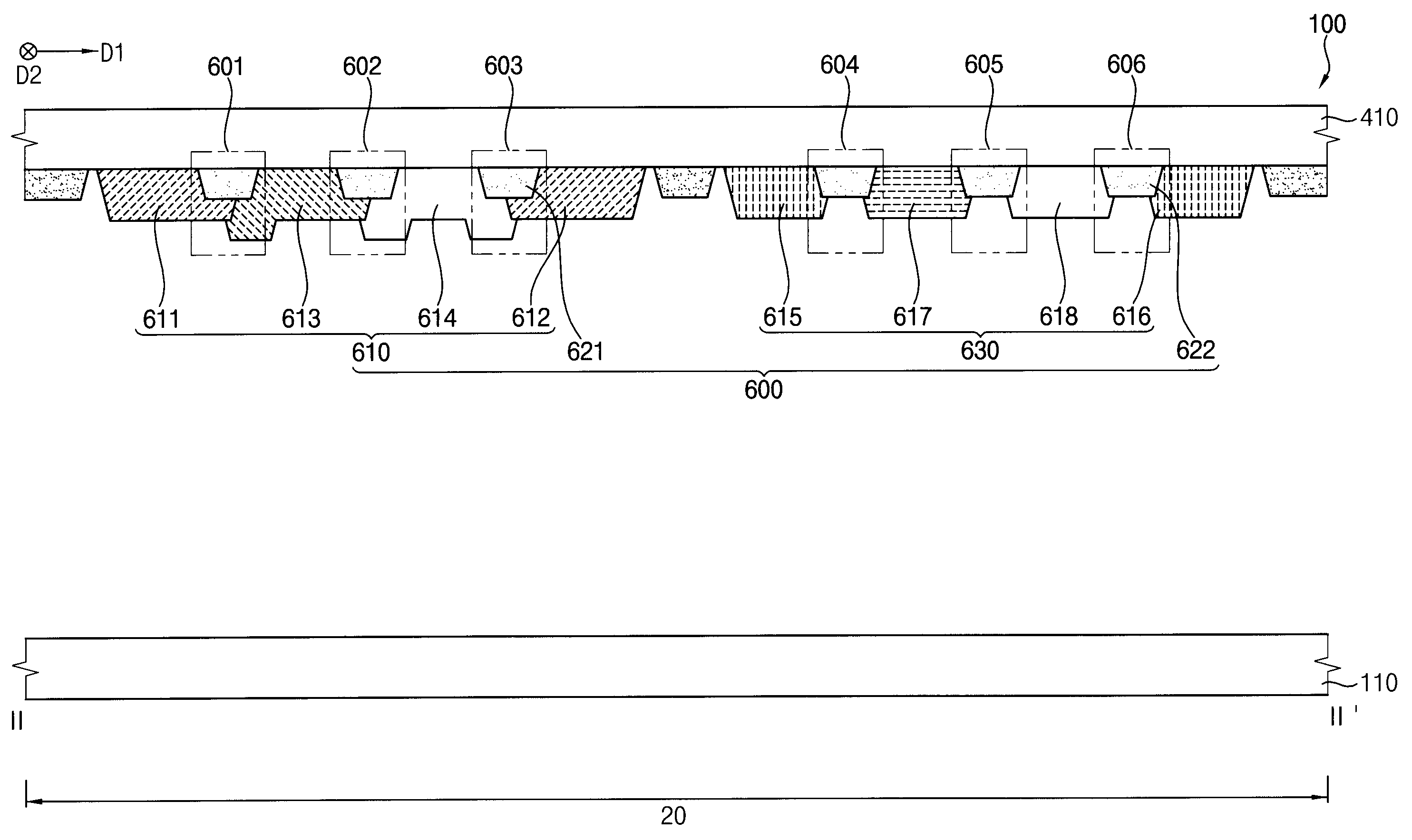
제1 개구(421) 및 제2 개구(422)는 하나의 쌍으로 서로 인접하여 주변 영역(20)에 위치할 수 있다. 다시 말하면, 제1 및 제2 개구들(421, 422)은 차광 패턴(420)의 4개의 모서리들 중 하나에 인접하여 위치할 수 있다. 또한, 제1 및 제2 개구들(421, 422)에는 상기 정렬 구조물이 배치될 수 있다. 여기서, 상기 정렬 구조물은 복수의 층들을 포함할 수 있고, 적어도 2개의 층들이 적층되는 복층 구조를 가질 수 있다. 예를 들면, 상기 정렬 구조물은 적어도 2개의 층들이 일 부분에서 서로 중첩할 수 있다. 더욱이, 제3 개구들(423)과 상기 제1 내지 제3 서브 화소 구조물들은 중첩할 수 있다. 즉, 상기 제1 내지 제3 서브 화소 구조물로부터 방출된 광이 제3 개구들(423)을 통해 외부로 방출될 수 있다.The first opening (421) and the second opening (422) may be adjacent to each other as a pair and may be positioned in the peripheral area (20). In other words, the first and second openings (421, 422) may be positioned adjacent to one of the four corners of the light-shielding pattern (420). In addition, the alignment structure may be arranged in the first and second openings (421, 422). Here, the alignment structure may include a plurality of layers and may have a multi-layer structure in which at least two layers are laminated. For example, the alignment structure may have at least two layers that overlap each other at one part. Furthermore, the third openings (423) and the first to third sub-pixel structures may overlap each other. That is, light emitted from the first to third sub-pixel structures may be emitted to the outside through the third openings (423).
다른 예시적인 실시예들에 있어서, 도 4에 도시된 바와 같이, 제1 및 제2 개구들(421, 422)이 4개의 모서리에 모두 위치할 수도 있다. 또 다른 예시적인 실시예들에 있어서, 도 5에 도시된 바와 같이, 복수의 제1 및 제2 개구들(421, 422)이 차광 패턴(420)의 주변 영역(20)에 위치할 수도 있다.In other exemplary embodiments, as illustrated in FIG. 4, the first and second openings (421, 422) may be located at all four corners. In still other exemplary embodiments, as illustrated in FIG. 5, a plurality of first and second openings (421, 422) may be located in the peripheral area (20) of the shading pattern (420).
상기 상부 기판과 상기 하부 기판 사이의 주변 영역(20)에 실링 패턴(390)이 배치될 수 있다. 실링 패턴(390)은 차광 패턴(420)으로부터 외측 방향으로 이격될 수 있고, 실질적으로 차광 패턴(420)을 둘러쌀 수 있다. 실링 패턴(390)에 의해 상기 상부 기판과 상기 하부 기판이 결합될 수 있다.A sealing pattern (390) may be arranged in a peripheral area (20) between the upper substrate and the lower substrate. The sealing pattern (390) may be spaced outwardly from the light-shielding pattern (420) and may substantially surround the light-shielding pattern (420). The upper substrate and the lower substrate may be coupled by the sealing pattern (390).
다만, 본 발명의 표시 영역(10), 주변 영역(20) 및 서브 화소 영역(30) 각각의 형상이 사각형의 평면 형상을 갖는 것으로 설명하였지만, 상기 형상이 이에 한정되는 것은 아니다. 예를 들면, 표시 영역(10), 주변 영역(20) 및 서브 화소 영역(30) 각각의 형상은 삼각형의 평면 형상, 마름모의 평면 형상, 다각형의 평면 형상, 원형의 평면 형상, 트랙형의 평면 형상 또는 타원형의 평면 형상을 가질 수도 있다.However, although the shapes of the display area (10), the peripheral area (20), and the sub-pixel area (30) of the present invention have been described as having a rectangular planar shape, the shape is not limited thereto. For example, the shapes of the display area (10), the peripheral area (20), and the sub-pixel area (30) may each have a triangular planar shape, a rhombus planar shape, a polygonal planar shape, a circular planar shape, a track-shaped planar shape, or an elliptical planar shape.
도 6은 도 3의 제1 및 제2 개구들에 배치된 정렬 패턴을 설명하기 위한 평면도이고, 도 7은 도 2의 I-I'라인을 따라 절단한 단면도이며, 도 8은 도 6의 II-II'라인을 따라 절단한 단면도이다.FIG. 6 is a plan view for explaining the alignment pattern arranged in the first and second openings of FIG. 3, FIG. 7 is a cross-sectional view taken along line I-I' of FIG. 2, and FIG. 8 is a cross-sectional view taken along line II-II' of FIG. 6.
도 6, 7 및 8을 참조하면, 표시 장치(100)는 하부 기판(110), 제1 반도체 소자(250_1), 제2 반도체 소자(250_2), 제3 반도체 소자(250_3), 게이트 절연층(150), 층간 절연층(190), 평탄화층(270), 제1 하부 전극(290_1), 제2 하부 전극(290_2), 제3 하부 전극(290_3), 발광층(330), 상부 전극(340), 박막 봉지 구조물(450), 제2 보호층(495), 광학 필터층(530), 제1 보호층(490). 컬러 필터층(510), 차광 패턴(420), 정렬 구조물(600), 실링 패턴(390), 상부 기판(410) 등을 포함할 수 있다. 여기서, 제1 하부 전극(290_1), 발광층(330) 및 상부 전극(340)을 제1 서브 화소 구조물로 정의하고, 제2 하부 전극(290_2), 발광층(330) 및 상부 전극(340)을 제2 서브 화소 구조물로 정의하며, 제3 하부 전극(290_3), 발광층(330) 및 상부 전극(340)을 제3 서브 화소 구조물로 정의한다. 예시적인 실시예들에 있어서, 차광 패턴(420)은 제1 개구(421), 제2 개구(422) 및 제3 개구들(423)을 가질 수 있고, 제1 및 제2 개구들(421, 422)에 정렬 구조물(600)이 배치될 수 있으며, 제3 개구들(423)에 상기 제1 내지 제3 화소 구조물들이 각기 중첩하여 위치할 수 있다.Referring to FIGS. 6, 7, and 8, the display device (100) may include a lower substrate (110), a first semiconductor element (250_1), a second semiconductor element (250_2), a third semiconductor element (250_3), a gate insulating layer (150), an interlayer insulating layer (190), a planarizing layer (270), a first lower electrode (290_1), a second lower electrode (290_2), a third lower electrode (290_3), a light-emitting layer (330), an upper electrode (340), a thin film encapsulation structure (450), a second protective layer (495), an optical filter layer (530), a first protective layer (490), a color filter layer (510), a light-shielding pattern (420), an alignment structure (600), a sealing pattern (390), an upper substrate (410), etc. Here, the first lower electrode (290_1), the light-emitting layer (330), and the upper electrode (340) are defined as a first sub-pixel structure, the second lower electrode (290_2), the light-emitting layer (330), and the upper electrode (340) are defined as a second sub-pixel structure, and the third lower electrode (290_3), the light-emitting layer (330), and the upper electrode (340) are defined as a third sub-pixel structure. In exemplary embodiments, the light-shielding pattern (420) may have a first opening (421), a second opening (422), and third openings (423), and alignment structures (600) may be arranged in the first and second openings (421, 422), and the first to third pixel structures may be positioned to overlap each other in the third openings (423).
제1 반도체 소자(250_1)는 제1 액티브층(130_1), 제1 게이트 전극(170_1), 제1 소스 전극(210_1) 및 제1 드레인 전극(230_1)을 포함할 수 있고, 제2 반도체 소자(250_2)는 제2 액티브층(130_2), 제2 게이트 전극(170_2), 제2 소스 전극(210_2) 및 제2 드레인 전극(230_2)을 포함할 수 있으며, 제3 반도체 소자(250_3)는 제3 액티브층(130_3), 제3 게이트 전극(170_3), 제3 소스 전극(210_3) 및 제3 드레인 전극(230_3)을 포함할 수 있다. 또한, 박막 봉지 구조물(450)은 제1 박막 봉지층(451), 제2 박막 봉지층(452) 및 제3 박막 봉지층(453)을 포함할 수 있고, 광학 필터층(530)은 제1 양자점 패턴(531), 산란 패턴(533) 및 제2 양자점 패턴(532)(예를 들어, 광학 필터 패턴들)을 포함할 수 있으며, 컬러 필터층(510)은 제1 컬러 필터 패턴(511), 제2 컬러 필터 패턴(512) 및 제3 컬러 필터 패턴(513)을 포함할 수 있다. 더욱이, 정렬 구조물(600)은 컬러 필터 정렬 패턴들(610), 제1 기준 정렬 패턴들(621), 광학 필터 정렬 패턴들(630) 및 제2 기준 정렬 패턴들(622)을 포함할 수 있고, 컬러 필터 정렬 패턴들(610)은 제1 컬러 필터 정렬 패턴(611), 제4 컬러 필터 정렬 패턴(612), 제2 컬러 필터 정렬 패턴(613) 및 제3 컬러 필터 정렬 패턴(614)을 포함할 수 있으며, 광학 필터 정렬 패턴들(630)은 제1 광학 필터 정렬 패턴(615), 제4 광학 필터 정렬 패턴(616), 제2 광학 필터 정렬 패턴(617) 및 제3 광학 필터 정렬 패턴(618)을 포함할 수 있다.The first semiconductor element (250_1) may include a first active layer (130_1), a first gate electrode (170_1), a first source electrode (210_1), and a first drain electrode (230_1), the second semiconductor element (250_2) may include a second active layer (130_2), a second gate electrode (170_2), a second source electrode (210_2), and a second drain electrode (230_2), and the third semiconductor element (250_3) may include a third active layer (130_3), a third gate electrode (170_3), a third source electrode (210_3), and a third drain electrode (230_3). Additionally, the thin film encapsulation structure (450) may include a first thin film encapsulation layer (451), a second thin film encapsulation layer (452), and a third thin film encapsulation layer (453), the optical filter layer (530) may include a first quantum dot pattern (531), a scattering pattern (533), and a second quantum dot pattern (532) (e.g., optical filter patterns), and the color filter layer (510) may include a first color filter pattern (511), a second color filter pattern (512), and a third color filter pattern (513). Moreover, the alignment structure (600) may include color filter alignment patterns (610), first reference alignment patterns (621), optical filter alignment patterns (630), and second reference alignment patterns (622), and the color filter alignment patterns (610) may include a first color filter alignment pattern (611), a fourth color filter alignment pattern (612), a second color filter alignment pattern (613), and a third color filter alignment pattern (614), and the optical filter alignment patterns (630) may include a first optical filter alignment pattern (615), a fourth optical filter alignment pattern (616), a second optical filter alignment pattern (617), and a third optical filter alignment pattern (618).
전술한 바와 같이, 표시 장치(100)는 복수의 서브 화소 영역들(30)을 포함하는 표시 영역(10) 및 표시 영역(10)을 둘러싸는 주변 영역(20)을 포함할 수 있다. 표시 장치(100)가 표시 영역(10) 및 주변 영역(20)을 포함함에 따라 하부 기판(110)도 표시 영역(10) 및 주변 영역(20)으로 구분될 수 있다.As described above, the display device (100) may include a display area (10) including a plurality of sub-pixel areas (30) and a peripheral area (20) surrounding the display area (10). As the display device (100) includes the display area (10) and the peripheral area (20), the lower substrate (110) may also be divided into the display area (10) and the peripheral area (20).
투명한 또는 불투명한 재료를 포함하는 하부 기판(110)이 제공될 수 있다. 하부 기판(110)은 석영(quartz) 기판, 합성 석영(synthetic quartz) 기판, 불화칼슘(calcium fluoride) 기판, 불소가 도핑된 석영(F-doped quartz) 기판, 소다라임(sodalime) 유리 기판, 무알칼리(non-alkali) 유리 기판 등을 포함할 수 있다.A lower substrate (110) including a transparent or opaque material may be provided. The lower substrate (110) may include a quartz substrate, a synthetic quartz substrate, a calcium fluoride substrate, a fluorine-doped quartz substrate, a sodalime glass substrate, a non-alkali glass substrate, and the like.
하부 기판(110) 상에 버퍼층(도시되지 않음)이 배치될 수도 있다. 상기 버퍼층은 하부 기판(110) 상에 전체적으로 배치될 수 있다. 상기 버퍼층은 하부 기판(110)으로부터 금속 원자들이나 불순물들이 반도체 소자 및 서브 화소 구조물로 확산되는 현상을 방지할 수 있으며, 액티브층을 형성하기 위한 결정화 공정 동안 열의 전달 속도를 조절하여 실질적으로 균일한 액티브층을 수득하게 할 수 있다. 또한, 상기 버퍼층은 하부 기판(110)의 표면이 균일하지 않을 경우, 하부 기판(110)의 표면의 평탄도를 향상시키는 역할을 수행할 수 있다. 하부 기판(110)의 유형에 따라 하부 기판(110) 상에 두 개 이상의 버퍼층이 제공될 수 있거나 상기 버퍼층이 배치되지 않을 수 있다. 예를 들면, 상기 버퍼층은 유기 물질 또는 무기 물질을 포함할 수도 있다.A buffer layer (not shown) may be disposed on the lower substrate (110). The buffer layer may be disposed entirely on the lower substrate (110). The buffer layer may prevent metal atoms or impurities from diffusing from the lower substrate (110) to the semiconductor element and the sub-pixel structure, and may control the heat transfer rate during the crystallization process for forming the active layer to obtain a substantially uniform active layer. In addition, the buffer layer may play a role of improving the flatness of the surface of the lower substrate (110) when the surface of the lower substrate (110) is not uniform. Depending on the type of the lower substrate (110), two or more buffer layers may be provided on the lower substrate (110), or the buffer layer may not be disposed. For example, the buffer layer may include an organic material or an inorganic material.
하부 기판(110) 상의 표시 영역(10)에 제1 내지 제3 액티브층들(130_1, 130_2, 130_3)이 서로 이격하여 배치될 수 있다. 제1 내지 제3 액티브층들(130_1, 130_2, 130_3) 각각은 산화물 반도체, 무기물 반도체(예를 들면, 아몰퍼스 실리콘(amorphous silicon), 폴리 실리콘(poly silicon)) 또는 유기물 반도체 등을 포함할 수 있고, 소스 영역 및 드레인 영역을 포함할 수 있다.First to third active layers (130_1, 130_2, 130_3) may be arranged spaced apart from each other in the display area (10) on the lower substrate (110). Each of the first to third active layers (130_1, 130_2, 130_3) may include an oxide semiconductor, an inorganic semiconductor (e.g., amorphous silicon, poly silicon), an organic semiconductor, etc., and may include a source region and a drain region.
제1 내지 제3 액티브층들(130_1, 130_2, 130_3) 상에는 게이트 절연층(150)이 배치될 수 있다. 게이트 절연층(150)은 하부 기판(110) 상의 표시 영역(10)에서 제1 내지 제3 액티브층들(130_1, 130_2, 130_3)을 덮을 수 있으며, 하부 기판(110) 상에 전체적으로 배치될 수 있다. 선택적으로, 게이트 절연층(150)이 하부 기판(110) 상의 주변 영역(20)에 배치될 수도 있다.A gate insulating layer (150) may be disposed on the first to third active layers (130_1, 130_2, 130_3). The gate insulating layer (150) may cover the first to third active layers (130_1, 130_2, 130_3) in the display area (10) on the lower substrate (110) and may be disposed entirely on the lower substrate (110). Optionally, the gate insulating layer (150) may also be disposed in the peripheral area (20) on the lower substrate (110).
예를 들면, 게이트 절연층(150)은 하부 기판(110) 상에서 제1 내지 제3 액티브층들(130_1, 130_2, 130_3)을 충분히 덮을 수 있으며, 제1 내지 제3 액티브층들(130_1, 130_2, 130_3)의주위에 단차를 생성시키지 않고 실질적으로 평탄한 상면을 가질 수 있다. 선택적으로, 게이트 절연층(150)은 하부 기판(110) 상에서 제1 내지 제3 액티브층들(130_1, 130_2, 130_3)을 덮으며, 균일한 두께로 제1 내지 제3 액티브층들(130_1, 130_2, 130_3)의 프로파일을 따라 배치될 수도 있다. 게이트 절연층(150)은 실리콘 화합물, 금속 산화물 등을 포함할 수 있다. 예를 들면, 게이트 절연층(150)은 실리콘 산화물(SiOx), 실리콘 질화물(SiNx), 실리콘 산질화물(SiOxNy), 실리콘 산탄화물(SiOxCy), 실리콘 탄질화물(SiCxNy), 알루미늄 산화물(AlOx), 알루미늄 질화물(AlNx), 탄탈륨 산화물(TaOx), 하프늄 산화물(HfOx), 지르코늄 산화물(ZrOx), 티타늄 산화물(TiOx) 등을 포함할 수 있다. 선택적으로, 게이트 절연층(150)은 복수의 절연층들을 포함하는 다층 구조를 가질 수도 있다. 예를 들면, 상기 절연층들은 두께가 서로 다르거나 서로 다른 물질을 포함할 수 있다.For example, the gate insulating layer (150) can sufficiently cover the first to third active layers (130_1, 130_2, 130_3) on the lower substrate (110) and can have a substantially flat upper surface without generating a step around the first to third active layers (130_1, 130_2, 130_3). Optionally, the gate insulating layer (150) can cover the first to third active layers (130_1, 130_2, 130_3) on the lower substrate (110) and can be arranged along the profile of the first to third active layers (130_1, 130_2, 130_3) with a uniform thickness. The gate insulating layer (150) can include a silicon compound, a metal oxide, or the like. For example, the gate insulating layer (150) may include silicon oxide (SiOx), silicon nitride (SiNx), silicon oxynitride (SiOxNy), silicon oxycarbide (SiOxCy), silicon carbonitride (SiCxNy), aluminum oxide (AlOx), aluminum nitride (AlNx), tantalum oxide (TaOx), hafnium oxide (HfOx), zirconium oxide (ZrOx), titanium oxide (TiOx), etc. Optionally, the gate insulating layer (150) may have a multilayer structure including a plurality of insulating layers. For example, the insulating layers may have different thicknesses or include different materials.
게이트 절연층(150) 상에 제1 내지 제3 게이트 전극들(170_1, 170_2, 170_3)이 서로 이격하여 배치될 수 있다. 예를 들면, 제1 게이트 전극(170_1)은 게이트 절연층(150) 중에서 하부에 제1 액티브층(130_1)이 위치하는 부분 상에 배치될 수 있고, 제2 게이트 전극(170_2)은 게이트 절연층(150) 중에서 하부에 제2 액티브층(130_2)이 위치하는 부분 상에 배치될 수 있으며, 제3 게이트 전극(170_3)은 게이트 절연층(150) 중에서 하부에 제3 액티브층(130_3)이 위치하는 부분 상에 배치될 수 있다. 제1 내지 제3 게이트 전극들(170_1, 170_2, 170_3) 각각은 금속, 합금, 금속 질화물, 도전성 금속 산화물, 투명 도전성 물질 등을 포함할 수 있다. 예를 들면, 제1 내지 제3 게이트 전극들(170_1, 170_2, 170_3) 각각은 금(Au), 은(Ag), 알루미늄(Al), 백금(Pt), 니켈(Ni), 티타늄(Ti), 팔라듐(Pd), 마그네슘(Mg), 칼슘(Ca), 리튬(Li), 크롬(Cr), 탄탈륨(Ta), 텅스텐(W), 구리(Cu), 몰리브데늄(Mo), 스칸듐(Sc), 네오디뮴(Nd), 이리듐(Ir), 알루미늄을 함유하는 합금, 알루미늄 질화물(AlNx), 은을 함유하는 합금, 텅스텐 질화물(WNx), 구리를 함유하는 합금, 몰리브데늄을 함유하는 합금, 티타늄 질화물(TiNx), 크롬 질화물(CrNx), 탄탈륨 질화물(TaNx), 스트론튬 루테늄 산화물(SrRuxOy), 아연 산화물(ZnOx), 인듐 주석 산화물(ITO), 주석 산화물(SnOx), 인듐 산화물(InOx), 갈륨 산화물(GaOx), 인듐 아연 산화물(IZO) 등을 포함할 수 있다. 이들은 단독으로 또는 서로 조합되어 사용될 수 있다. 선택적으로, 제1 내지 제3 게이트 전극들(170_1, 170_2, 170_3) 각각은 복수의 층들을 포함하는 다층 구조를 가질 수도 있다.First to third gate electrodes (170_1, 170_2, 170_3) may be arranged spaced apart from each other on the gate insulating layer (150). For example, the first gate electrode (170_1) may be arranged on a portion of the gate insulating layer (150) where the first active layer (130_1) is positioned underneath, the second gate electrode (170_2) may be arranged on a portion of the gate insulating layer (150) where the second active layer (130_2) is positioned underneath, and the third gate electrode (170_3) may be arranged on a portion of the gate insulating layer (150) where the third active layer (130_3) is positioned underneath. Each of the first to third gate electrodes (170_1, 170_2, 170_3) may include a metal, an alloy, a metal nitride, a conductive metal oxide, a transparent conductive material, or the like. For example, each of the first to third gate electrodes (170_1, 170_2, 170_3) may be formed of gold (Au), silver (Ag), aluminum (Al), platinum (Pt), nickel (Ni), titanium (Ti), palladium (Pd), magnesium (Mg), calcium (Ca), lithium (Li), chromium (Cr), tantalum (Ta), tungsten (W), copper (Cu), molybdenum (Mo), scandium (Sc), neodymium (Nd), iridium (Ir), an alloy containing aluminum, aluminum nitride (AlNx), an alloy containing silver, tungsten nitride (WNx), an alloy containing copper, an alloy containing molybdenum, titanium nitride (TiNx), chromium nitride (CrNx), tantalum nitride (TaNx), strontium ruthenium oxide (SrRuxOy), zinc oxide (ZnOx), indium tin oxide (ITO), tin. It may include oxide (SnOx), indium oxide (InOx), gallium oxide (GaOx), indium zinc oxide (IZO), etc. These may be used alone or in combination with each other. Optionally, each of the first to third gate electrodes (170_1, 170_2, 170_3) may have a multilayer structure including a plurality of layers.
제1 내지 제3 게이트 전극들(170_1, 170_2, 170_3) 상에는 층간 절연층(190)이 배치될 수 있다. 층간 절연층(190)은 게이트 절연층(150) 상의 표시 영역(10)에서 제1 내지 제3 게이트 전극들(170_1, 170_2, 170_3)을 덮을 수 있으며, 게이트 절연층(150) 상에서 전체적으로 배치될 수 있다. 선택적으로, 층간 절연층(190)은 하부 기판(110) 상의 주변 영역(20)에 배치될 수도 있다.An interlayer insulating layer (190) may be disposed on the first to third gate electrodes (170_1, 170_2, 170_3). The interlayer insulating layer (190) may cover the first to third gate electrodes (170_1, 170_2, 170_3) in the display area (10) on the gate insulating layer (150) and may be disposed entirely on the gate insulating layer (150). Optionally, the interlayer insulating layer (190) may also be disposed in the peripheral area (20) on the lower substrate (110).
예를 들면, 층간 절연층(190)은 게이트 절연층(150) 상에서 제1 내지 제3 게이트 전극들(170_1, 170_2, 170_3)을 충분히 덮을 수 있으며, 제1 내지 제3 게이트 전극들(170_1, 170_2, 170_3)의 주위에 단차를 생성시키지 않고 실질적으로 평탄한 상면을 가질 수 있다. 선택적으로, 층간 절연층(190)은 게이트 절연층(150) 상에서 제1 내지 제3 게이트 전극들(170_1, 170_2, 170_3)을 덮으며, 균일한 두께로 제1 내지 제3 게이트 전극들(170_1, 170_2, 170_3)의 프로파일을 따라 배치될 수도 있다. 층간 절연층(190)은 실리콘 화합물, 금속 산화물 등을 포함할 수 있다. 선택적으로, 층간 절연층(190)은 복수의 절연층들을 포함하는 다층 구조를 가질 수도 있다. 예를 들면, 상기 절연층들은 두께가 서로 다르거나 서로 다른 물질을 포함할 수 있다.For example, the interlayer insulating layer (190) can sufficiently cover the first to third gate electrodes (170_1, 170_2, 170_3) on the gate insulating layer (150) and can have a substantially flat upper surface without generating a step around the first to third gate electrodes (170_1, 170_2, 170_3). Optionally, the interlayer insulating layer (190) can cover the first to third gate electrodes (170_1, 170_2, 170_3) on the gate insulating layer (150) and can be arranged along the profile of the first to third gate electrodes (170_1, 170_2, 170_3) with a uniform thickness. The interlayer insulating layer (190) can include a silicon compound, a metal oxide, or the like. Optionally, the interlayer insulation layer (190) may have a multilayer structure including a plurality of insulation layers. For example, the insulation layers may have different thicknesses or include different materials.
층간 절연층(190) 상의 표시 영역(10)에는 제1 소스 전극(210_1), 제1 드레인 전극(230_1), 제2 소스 전극(210_2), 제2 드레인 전극(230_2), 제3 소스 전극(210_3) 및 제3 드레인 전극(230_3)이 서로 이격하여 배치될 수 있다. 예를 들면, 제1 소스 전극(210_1)은 게이트 절연층(150) 및 층간 절연층(190)의 제1 부분을 제거하여 형성된 콘택홀을 통해 제1 액티브층(130_1)의 소스 영역에 접속될 수 있고, 제1 드레인 전극(230_1)은 게이트 절연층(150) 및 층간 절연층(190)의 제2 부분을 제거하여 형성된 콘택홀을 통해 제1 액티브층(130_1)의 드레인 영역에 접속될 수 있다. 또한, 제2 소스 전극(210_2)은 게이트 절연층(150) 및 층간 절연층(190)의 제3 부분을 제거하여 형성된 콘택홀을 통해 제2 액티브층(130_2)의 소스 영역에 접속될 수 있고, 제2 드레인 전극(230_2)은 게이트 절연층(150) 및 층간 절연층(190)의 제4 부분을 제거하여 형성된 콘택홀을 통해 제2 액티브층(130_2)의 드레인 영역에 접속될 수 있다. 더욱이, 제3 소스 전극(210_3)은 게이트 절연층(150) 및 층간 절연층(190)의 제5 부분을 제거하여 형성된 콘택홀을 통해 제3 액티브층(130_3)의 소스 영역에 접속될 수 있고, 제3 드레인 전극(230_3)은 게이트 절연층(150) 및 층간 절연층(190)의 제6 부분을 제거하여 형성된 콘택홀을 통해 제3 액티브층(130_3)의 드레인 영역에 접속될 수 있다. 제1 내지 제3 소스 전극들(210_1, 210_2, 210_3) 및 제1 내지 제3 드레인 전극들(230_1, 230_2, 230_3) 각각은 각기 금속, 합금, 금속 질화물, 도전성 금속 산화물, 투명 도전성 물질 등을 포함할 수 있다. 이들은 단독으로 또는 서로 조합되어 사용될 수 있다. 선택적으로, 제1 내지 제3 소스 전극들(210_1, 210_2, 210_3) 및 제1 내지 제3 드레인 전극들(230_1, 230_2, 230_3) 각각은 복수의 층들을 포함하는 다층 구조를 가질 수도 있다. In the display area (10) on the interlayer insulating layer (190), a first source electrode (210_1), a first drain electrode (230_1), a second source electrode (210_2), a second drain electrode (230_2), a third source electrode (210_3), and a third drain electrode (230_3) may be arranged to be spaced apart from each other. For example, the first source electrode (210_1) may be connected to the source region of the first active layer (130_1) through a contact hole formed by removing a first portion of the gate insulating layer (150) and the interlayer insulating layer (190), and the first drain electrode (230_1) may be connected to the drain region of the first active layer (130_1) through a contact hole formed by removing a second portion of the gate insulating layer (150) and the interlayer insulating layer (190). Additionally, the second source electrode (210_2) can be connected to the source region of the second active layer (130_2) through a contact hole formed by removing the third portion of the gate insulating layer (150) and the interlayer insulating layer (190), and the second drain electrode (230_2) can be connected to the drain region of the second active layer (130_2) through a contact hole formed by removing the fourth portion of the gate insulating layer (150) and the interlayer insulating layer (190). Furthermore, the third source electrode (210_3) can be connected to the source region of the third active layer (130_3) through a contact hole formed by removing the fifth portion of the gate insulating layer (150) and the interlayer insulating layer (190), and the third drain electrode (230_3) can be connected to the drain region of the third active layer (130_3) through a contact hole formed by removing the sixth portion of the gate insulating layer (150) and the interlayer insulating layer (190). Each of the first to third source electrodes (210_1, 210_2, 210_3) and the first to third drain electrodes (230_1, 230_2, 230_3) may include a metal, an alloy, a metal nitride, a conductive metal oxide, a transparent conductive material, or the like. These may be used alone or in combination with each other. Optionally, each of the first to third source electrodes (210_1, 210_2, 210_3) and the first to third drain electrodes (230_1, 230_2, 230_3) may have a multilayer structure including a plurality of layers.
이에 따라, 제1 액티브층(130_1), 제1 게이트 전극(170_1), 제1 소스 전극(210_1) 및 제1 드레인 전극(230_1)을 포함하는 제1 반도체 소자(250_1)가 배치될 수 있고, 제2 액티브층(130_2), 제2 게이트 전극(170_2), 제2 소스 전극(210_2) 및 제2 드레인 전극(230_2)을 포함하는 제2 반도체 소자(250_2)가 배치될 수 있으며, 제3 액티브층(130_3), 제3 게이트 전극(170_3), 제3 소스 전극(210_3) 및 제3 드레인 전극(230_3)을 포함하는 제3 반도체 소자(250_3)가 배치될 수 있다.Accordingly, a first semiconductor element (250_1) including a first active layer (130_1), a first gate electrode (170_1), a first source electrode (210_1), and a first drain electrode (230_1) can be arranged, a second semiconductor element (250_2) including a second active layer (130_2), a second gate electrode (170_2), a second source electrode (210_2), and a second drain electrode (230_2) can be arranged, and a third semiconductor element (250_3) including a third active layer (130_3), a third gate electrode (170_3), a third source electrode (210_3), and a third drain electrode (230_3) can be arranged.
다만, 표시 장치(100)가 3개의 트랜지스터들(예를 들어, 제1 내지 제3 반도체 소자들(250_1, 250_2, 250_3))을 포함하는 구성을 갖는 것으로 설명하였으나, 본 발명의 구성이 이에 한정되는 것은 아니다. 예를 들면, 표시 장치(100)는 복수의 트랜지스터들 및 적어도 복수의 커패시터들을 포함하는 구성을 가질 수도 있다.However, although the display device (100) has been described as having a configuration including three transistors (for example, the first to third semiconductor elements (250_1, 250_2, 250_3)), the configuration of the present invention is not limited thereto. For example, the display device (100) may have a configuration including a plurality of transistors and at least a plurality of capacitors.
또한, 제1 내지 제3 반도체 소자들(250_1, 250_2, 250_3) 각각이 상부 게이트 구조를 갖는 것으로 설명하였으나, 본 발명의 구성이 이에 한정되는 것은 아니다. 예를 들면, 제1 내지 제3 반도체 소자들(250_1, 250_2, 250_3) 각각은 하부 게이트 구조 및/또는 더블 게이트 구조를 가질 수도 있다.In addition, although each of the first to third semiconductor elements (250_1, 250_2, 250_3) has been described as having an upper gate structure, the configuration of the present invention is not limited thereto. For example, each of the first to third semiconductor elements (250_1, 250_2, 250_3) may have a lower gate structure and/or a double gate structure.
더욱이, 제1 내지 제3 반도체 소자들(250_1, 250_2, 250_3) 각각의 구성에 게이트 절연층(150) 및 층간 절연층(190)이 포함되지 않는 것으로 설명하였으나, 본 발명이 이에 한정되는 것은 아니다. 예를 들면, 제1 내지 제3 반도체 소자들(250_1, 250_2, 250_3) 각각의 구성에 게이트 절연층(150) 및 층간 절연층(190)이 포함될 수도 있다.Furthermore, although it has been described that the gate insulating layer (150) and the interlayer insulating layer (190) are not included in the configuration of each of the first to third semiconductor elements (250_1, 250_2, 250_3), the present invention is not limited thereto. For example, the gate insulating layer (150) and the interlayer insulating layer (190) may be included in the configuration of each of the first to third semiconductor elements (250_1, 250_2, 250_3).
층간 절연층(190) 및 제1 내지 제3 반도체 소자들(250_1, 250_2, 250_3) 상의 표시 영역(10)에 평탄화층(270)이 배치될 수 있고, 주변 영역(20)에는 배치되지 않을 수 있다. 예를 들면, 평탄화층(270)은 층간 절연층(190) 상에서 제1 내지 제3 소스 전극들(210_1, 210_2, 210_3) 및 제1 내지 제3 드레인 전극들(230_1, 230_2, 230_3)을 충분히 덮도록 상대적으로 두꺼운 두께로 배치될 수 있고, 이러한 경우, 평탄화층(270)은 실질적으로 평탄한 상면을 가질 수 있으며, 이와 같은 평탄화층(270)의 평탄한 상면을 구현하기 위하여 평탄화층(270)에 대해 평탄화 공정이 추가될 수 있다. 평탄화층(270)은 유기 물질 또는 무기 물질 등을 포함할 수 있다. 예시적인 실시예들에 있어서, 평탄화층(270)은 유기 물질을 포함할 수 있다.A planarization layer (270) may be disposed on the display area (10) on the interlayer insulating layer (190) and the first to third semiconductor elements (250_1, 250_2, 250_3), and may not be disposed on the peripheral area (20). For example, the planarization layer (270) may be disposed with a relatively thick thickness so as to sufficiently cover the first to third source electrodes (210_1, 210_2, 210_3) and the first to third drain electrodes (230_1, 230_2, 230_3) on the interlayer insulating layer (190), and in this case, the planarization layer (270) may have a substantially flat upper surface, and a flattening process may be added to the planarization layer (270) to implement a flat upper surface of such a planarization layer (270). The flattening layer (270) may include an organic material or an inorganic material. In exemplary embodiments, the flattening layer (270) may include an organic material.
평탄화층(270) 상의 표시 영역(10)에 제1 내지 제3 하부 전극들(290_1, 290_2, 290_3)이 서로 이격하여 배치될 수 있다. 예를 들면, 제1 하부 전극(290_1)이 평탄화층(270)의 제1 부분에 배치될 수 있고, 제2 하부 전극(290_2)이 평탄화층(270)의 제2 부분에 배치될 수 있으며, 제3 하부 전극(290_3)이 평탄화층(270)의 제3 부분에 배치될 수 있다. 여기서, 평탄화층(270)의 상기 제3 부분은 상기 제1 부분으로부터 이격하여 위치할 수 있고, 평탄화층(270)의 상기 제2 부분은 상기 제1 부분과 상기 제3 부분 사이에 위치할 수 있다. 다시 말하면, 상기 제1, 제2 및 제3 부분들은 차광 패턴(420)의 제3 개구들(423)과 중첩할 수 있다.First to third lower electrodes (290_1, 290_2, 290_3) may be arranged spaced apart from each other in the display area (10) on the flattening layer (270). For example, the first lower electrode (290_1) may be arranged on a first portion of the flattening layer (270), the second lower electrode (290_2) may be arranged on a second portion of the flattening layer (270), and the third lower electrode (290_3) may be arranged on a third portion of the flattening layer (270). Here, the third portion of the flattening layer (270) may be positioned spaced apart from the first portion, and the second portion of the flattening layer (270) may be positioned between the first portion and the third portion. In other words, the first, second and third portions can overlap with the third openings (423) of the shading pattern (420).
제1 내지 제3 하부 전극들(290_1, 290_2, 290_3) 각각은 평탄화층(270)을 관통하여 제1 내지 제3 드레인 전극들(230_1, 230_2, 230_3)에 각기 접속될 수 있다. 즉, 제1 내지 제3 하부 전극들(290_1, 290_2, 290_3) 각각은 제1 내지 제3 반도체 소자들(250_1, 250_2, 250_3) 각각과 전기적으로 연결될 수 있다. 제1 내지 제3 하부 전극들(290_1, 290_2, 290_3) 각각은 금속, 합금, 금속 질화물, 도전성 금속 산화물, 투명 도전성 물질 등을 포함할 수 있다. 이들은 단독으로 또는 서로 조합되어 사용될 수 있다. 선택적으로, 제1 내지 제3 하부 전극들(290_1, 290_2, 290_3) 각각은 복수의 층들을 포함하는 다층 구조를 가질 수도 있다.Each of the first to third lower electrodes (290_1, 290_2, 290_3) may be connected to each of the first to third drain electrodes (230_1, 230_2, 230_3) by penetrating the planarization layer (270). That is, each of the first to third lower electrodes (290_1, 290_2, 290_3) may be electrically connected to each of the first to third semiconductor elements (250_1, 250_2, 250_3). Each of the first to third lower electrodes (290_1, 290_2, 290_3) may include a metal, an alloy, a metal nitride, a conductive metal oxide, a transparent conductive material, or the like. These may be used alone or in combination with each other. Optionally, each of the first to third lower electrodes (290_1, 290_2, 290_3) may have a multilayer structure including multiple layers.
화소 정의막(310)은 제1 내지 제3 하부 전극들(290_1, 290_2, 290_3) 각각의 일부 및 평탄화층(270) 상의 표시 영역(10)에 배치될 수 있고, 주변 영역(20)에는 배치되지 않을 수 있다. 화소 정의막(310)은 제1 내지 제3 하부 전극들(290_1, 290_2, 290_3) 각각의 양측부를 덮을 수 있고, 제1 내지 제3 하부 전극들(290_1, 290_2, 290_3) 각각의 상면의 일부를 노출시킬 수 있다. 화소 정의막(310)은 유기 물질 또는 무기 물질로 이루어질 수 있다. 예시적인 실시예들에 있어서, 화소 정의막(310)은 유기 물질을 포함할 수 있다.The pixel defining film (310) may be disposed on a portion of each of the first to third lower electrodes (290_1, 290_2, 290_3) and the display area (10) on the planarization layer (270), and may not be disposed in the peripheral area (20). The pixel defining film (310) may cover both sides of each of the first to third lower electrodes (290_1, 290_2, 290_3), and may expose a portion of the upper surface of each of the first to third lower electrodes (290_1, 290_2, 290_3). The pixel defining film (310) may be made of an organic material or an inorganic material. In exemplary embodiments, the pixel defining film (310) may include an organic material.
발광층(330)은 화소 정의막(310)에 의해 노출된 제1 내지 제3 하부 전극들(290_1, 290_2, 290_3) 상의 표시 영역(10)에 배치될 수 있다. 다시 말하면, 발광층(330)은 하부 기판(110) 상의 표시 영역(10)에서 연속적으로 배치될 수 있고, 표시 영역(10)에서 일체로 형성될 수 있다. 예시적인 실시예들에 있어서, 발광층(330)은 청색광을 방출시킬 수 있는 발광 물질을 사용하여 형성될 수 있다. 이와는 달리, 발광층(330)은 적색광, 녹색광, 청색광 등의 다른 색광들을 발생시킬 수 있는 복수의 발광 물질들을 적층하여 전체적으로 백색광을 방출할 수도 있다.The light-emitting layer (330) may be arranged in the display area (10) on the first to third lower electrodes (290_1, 290_2, 290_3) exposed by the pixel defining film (310). In other words, the light-emitting layer (330) may be arranged continuously in the display area (10) on the lower substrate (110) and may be formed integrally in the display area (10). In exemplary embodiments, the light-emitting layer (330) may be formed using a light-emitting material capable of emitting blue light. Alternatively, the light-emitting layer (330) may emit white light overall by stacking a plurality of light-emitting materials capable of emitting other color lights, such as red light, green light, and blue light.
상부 전극(340)은 화소 정의막(310) 및 발광층(330) 상의 표시 영역(10)에 배치될 수 있다. 상부 전극(340)은 금속, 합금, 금속 질화물, 도전성 금속 산화물, 투명 도전성 물질 등을 포함할 수 있다. 이들은 단독으로 또는 서로 조합되어 사용될 수 있다. 선택적으로, 상부 전극(340)은 복수의 층들을 포함하는 다층 구조를 가질 수도 있다.The upper electrode (340) may be placed in the display area (10) on the pixel defining film (310) and the light emitting layer (330). The upper electrode (340) may include a metal, an alloy, a metal nitride, a conductive metal oxide, a transparent conductive material, etc. These may be used alone or in combination with each other. Optionally, the upper electrode (340) may have a multilayer structure including a plurality of layers.
이에 따라, 제1 하부 전극(290_1), 발광층(330) 및 상부 전극(340)을 포함하는 상기 제1 서브 화소 구조물이 배치될 수 있고, 제2 하부 전극(290_2), 발광층(330) 및 상부 전극(340)을 포함하는 상기 제2 서브 화소 구조물이 배치될 수 있으며, 제3 하부 전극(290_3), 발광층(330) 및 상부 전극(340)을 포함하는 상기 제3 서브 화소 구조물이 배치될 수 있다.Accordingly, the first sub-pixel structure including the first lower electrode (290_1), the light-emitting layer (330), and the upper electrode (340) can be arranged, the second sub-pixel structure including the second lower electrode (290_2), the light-emitting layer (330), and the upper electrode (340) can be arranged, and the third sub-pixel structure including the third lower electrode (290_3), the light-emitting layer (330), and the upper electrode (340) can be arranged.
상부 전극(340) 상에 제1 박막 봉지층(451)이 배치될 수 있다. 제1 박막 봉지층(451)은 상부 전극(340)을 덮으며, 균일한 두께로 상부 전극(340)의 프로 파일을 따라 배치될 수 있다. 선택적으로, 제1 박막 봉지층(451)이 하부 기판(110) 상의 주변 영역(20)에 배치될 수도 있다. 제1 박막 봉지층(451)은 상기 제1 내지 제3 서브 화소 구조물들이 수분, 산소 등의 침투로 인해 열화되는 것을 방지할 수 있다. 또한, 제1 박막 봉지층(451)은 외부의 충격으로부터 상기 제1 내지 제3 서브 화소 구조물들을 보호하는 기능도 수행할 수 있다. 제1 박막 봉지층(451)은 가요성을 갖는 무기 물질들을 포함할 수 있다.A first thin film encapsulation layer (451) may be disposed on the upper electrode (340). The first thin film encapsulation layer (451) covers the upper electrode (340) and may be disposed along the profile of the upper electrode (340) with a uniform thickness. Optionally, the first thin film encapsulation layer (451) may be disposed in a peripheral region (20) on the lower substrate (110). The first thin film encapsulation layer (451) may prevent the first to third sub-pixel structures from being deteriorated due to penetration of moisture, oxygen, etc. In addition, the first thin film encapsulation layer (451) may also perform a function of protecting the first to third sub-pixel structures from external impact. The first thin film encapsulation layer (451) may include inorganic materials having flexibility.
제1 박막 봉지층(451) 상에 제2 박막 봉지층(452)이 배치될 수 있다. 제2 박막 봉지층(452)은 표시 장치(100)의 평탄도를 향상시킬 수 있으며, 상기 제1 내지 제3 서브 화소 구조물들을 보호할 수 있다. 제2 박막 봉지층(452) 가요성을 갖는 유기 물질들을 포함할 수 있다.A second thin film encapsulation layer (452) may be disposed on the first thin film encapsulation layer (451). The second thin film encapsulation layer (452) may improve the flatness of the display device (100) and protect the first to third sub-pixel structures. The second thin film encapsulation layer (452) may include organic materials having flexibility.
제2 박막 봉지층(452) 상에 제3 박막 봉지층(453)이 배치될 수 있다. 제3 박막 봉지층(453)은 제2 박막 봉지층(452)을 덮으며, 균일한 두께로 제2 박막 봉지층(452)의 프로 파일을 따라 배치될 수 있다. 선택적으로, 제3 박막 봉지층(453)이 하부 기판(110) 상의 주변 영역(20)에 배치될 수도 있다. 제3 박막 봉지층(453)은 제1 박막 봉지층(451)과 함께 상기 제1 내지 제3 서브 화소 구조물들이 수분, 산소 등의 침투로 인해 열화되는 것을 방지할 수 있다. 또한, 제3 박막 봉지층(453)은 외부의 충격으로부터 제1 박막 봉지층(451) 및 제2 박막 봉지층(452)과 함께 상기 제1 내지 제3 서브 화소 구조물들을 보호하는 기능도 수행할 수 있다. 제3 박막 봉지층(453)은 상기 가요성을 갖는 무기 물질들을 포함할 수 있다.A third thin film encapsulation layer (453) may be disposed on the second thin film encapsulation layer (452). The third thin film encapsulation layer (453) covers the second thin film encapsulation layer (452) and may be disposed along the profile of the second thin film encapsulation layer (452) with a uniform thickness. Optionally, the third thin film encapsulation layer (453) may be disposed in a peripheral area (20) on the lower substrate (110). The third thin film encapsulation layer (453), together with the first thin film encapsulation layer (451), may prevent the first to third sub-pixel structures from being deteriorated due to the penetration of moisture, oxygen, etc. In addition, the third thin film encapsulation layer (453) may also perform a function of protecting the first to third sub-pixel structures from external impact together with the first thin film encapsulation layer (451) and the second thin film encapsulation layer (452). The third thin film encapsulation layer (453) may include inorganic materials having the above flexibility.
이에 따라, 제1 박막 봉지층(451), 제2 박막 봉지층(452) 및 제3 박막 봉지층(453)을 포함하는 박막 봉지 구조물(450)이 배치될 수 있다. 선택적으로, 박막 봉지 구조물(450)은 제1 내지 제5 박막 봉지층들로 적층된 5층 구조 또는 제1 내지 제7 박막 봉지층들로 적층된 7층 구조로 구성될 수도 있다.Accordingly, a thin film encapsulation structure (450) including a first thin film encapsulation layer (451), a second thin film encapsulation layer (452), and a third thin film encapsulation layer (453) can be arranged. Optionally, the thin film encapsulation structure (450) can be configured as a five-layer structure laminated with the first to fifth thin film encapsulation layers or a seven-layer structure laminated with the first to seventh thin film encapsulation layers.
박막 봉지 구조물(450) 상에 상부 기판(410)이 배치될 수 있다. 상부 기판(410)은 하부 기판(110)과 마주보도록 배치될 수 있다. 상부 기판(410)과 하부 기판(110)은 실질적으로 동일한 물질을 포함할 수 있다. 예를 들면, 상부 기판(410)은 석영 기판, 합성 석영 기판, 불화칼슘 기판, 불소가 도핑된 석영 기판, 소다라임 유리 기판, 무알칼리 유리 기판 등을 포함할 수 있다.An upper substrate (410) may be placed on a thin film encapsulation structure (450). The upper substrate (410) may be placed to face the lower substrate (110). The upper substrate (410) and the lower substrate (110) may include substantially the same material. For example, the upper substrate (410) may include a quartz substrate, a synthetic quartz substrate, a calcium fluoride substrate, a fluorine-doped quartz substrate, a soda lime glass substrate, an alkali-free glass substrate, and the like.
도 7 및 8에 도시된 바와 같이, 상부 기판(410)의 저면 상의 표시 영역(10) 및 주변 영역(20)의 일부에 차광 패턴(420)이 배치될 수 있다. 다시 말하면, 상부 기판(410)과 광학 필터층(530) 사이에 차광 패턴(420)이 배치될 수 있다. 전술한 바와 같이, 차광 패턴(420)은 표시 영역(10)에서 제3 개구들(423)을 가질 수 있고, 주변 영역(20)에서 제1 개구(421) 및 제2 개구(422)를 가질 수 있다. 제3 개구(423)는 상기 제1 내지 제3 서브 화소 구조물들 각각과 중첩할 수 있고, 제1 개구(421)에는 컬러 필터 정렬 패턴들(610)이 배치될 수 있으며, 제2 개구(422)에는 광학 필터 정렬 패턴들(630)이 배치될 수 있다. 차광 패턴(420)은 포토레지스트(photoresist), 폴리아크릴계 수지(polyacryl-based region), 폴리이미드계 수지(polyimide-based resin), 폴리아미드계 수지(polyamide-based resin), 실록산계 수지(siloxane-based resin), 아크릴계 수지(acryl-based resin), 에폭시계 수지(epoxy-based resin) 등과 같은 유기 물질을 포함할 수 있다. 또한, 차광 패턴(420)은 실질적으로 불투명할 수 있다. 예를 들면, 차광 패턴(420)은 광을 흡수하기 위해 차광 재료를 더 포함할 수 있다. 상기 차광 재료는 카본 블랙(carbon black), 산질화 티타늄(titanium nitride oxide), 티타늄 블랙(titanium black), 페닐렌 블랙(phenylene black), 아닐린 블랙(aniline black), 시아닌 블랙(cyanine black), 니그로신산 블랙(nigrosine acid black), 블랙 수지(black resin) 등을 포함할 수 있다.As illustrated in FIGS. 7 and 8, a light-shielding pattern (420) may be disposed on a portion of the display area (10) and the peripheral area (20) on the lower surface of the upper substrate (410). In other words, the light-shielding pattern (420) may be disposed between the upper substrate (410) and the optical filter layer (530). As described above, the light-shielding pattern (420) may have third openings (423) in the display area (10), and may have first openings (421) and second openings (422) in the peripheral area (20). The third opening (423) may overlap each of the first to third sub-pixel structures, and color filter alignment patterns (610) may be disposed in the first opening (421), and optical filter alignment patterns (630) may be disposed in the second opening (422). The light-shielding pattern (420) may include an organic material such as a photoresist, a polyacryl-based resin, a polyimide-based resin, a polyamide-based resin, a siloxane-based resin, an acrylic resin, an epoxy-based resin, and the like. In addition, the light-shielding pattern (420) may be substantially opaque. For example, the light-shielding pattern (420) may further include a light-shielding material to absorb light. The light-shielding material may include carbon black, titanium nitride oxide, titanium black, phenylene black, aniline black, cyanine black, nigrosine acid black, a black resin, and the like.
차광 패턴(420)의 제3 개구들(423)에 컬러 필터층(510)이 배치될 수 있다. 다시 말하면, 제3 개구들(423)에서 상부 기판(410)의 저면 상에 컬러 필터층(510)이 배치될 수 있다. 예시적인 실시예들에 있어서, 컬러 필터층(510)은 차광 패턴(420)과 부분적으로 중첩할 수 있다. 컬러 필터층(510)은 녹색광을 투과시키는 제1 컬러 필터 패턴(511), 청색광을 투과시키는 제2 컬러 필터 패턴(512) 및 적색광을 투과시키는 제3 컬러 필터 패턴(513)을 포함할 수 있다. 예시적인 실시예들에 있어서, 제1 컬러 필터 패턴(511), 제2 컬러 필터 패턴(512) 및 제3 컬러 필터 패턴(513) 각각은 제1 폭을 가질 수 있다.A color filter layer (510) may be disposed in the third openings (423) of the shading pattern (420). In other words, the color filter layer (510) may be disposed on the lower surface of the upper substrate (410) in the third openings (423). In exemplary embodiments, the color filter layer (510) may partially overlap the shading pattern (420). The color filter layer (510) may include a first color filter pattern (511) that transmits green light, a second color filter pattern (512) that transmits blue light, and a third color filter pattern (513) that transmits red light. In exemplary embodiments, each of the first color filter pattern (511), the second color filter pattern (512), and the third color filter pattern (513) may have a first width.
예를 들면, 제1 컬러 필터 패턴(511)은 도 7에 도시된 제3 개구들(423) 중 좌측에 위치하는 제3 개구(423)에 배치될 수 있고, 제2 컬러 필터 패턴(512)은 도 7에 도시된 제3 개구들(423) 중 가운데에 위치하는 제3 개구(423)에 배치될 수 있으며, 제3 컬러 필터 패턴(513)은 도 7에 도시된 제3 개구들(423) 중 우측에 위치하는 제3 개구(423)에 배치될 수 있다. 다시 말하면, 제1 컬러 필터 패턴(511)은 제1 양자점 패턴(531) 상에 배치될 수 있고, 제2 컬러 필터 패턴(512)은 산란 패턴(533) 상에 배치될 수 있으며, 제3 컬러 필터 패턴(513)은 제2 양자점 패턴(532) 상에 배치될 수 있다. 여기서, 상부 기판(410)의 저면 상에서 제1 컬러 필터 패턴(511), 제2 컬러 필터 패턴(512) 및 제3 컬러 필터 패턴(513)은 반복적으로 배열될 수 있다. 이에 따라, 제1 컬러 필터 패턴(511)의 좌측에 배치되는 제3 컬러 필터 패턴의 일부가 제1 컬러 필터 패턴(511)과 차광 패턴(420) 사이에 도시될 수 있고(도 13 참조), 제3 컬러 필터 패턴(513)의 우측에 배치되는 제1 컬러 필터 패턴의 일부가 제3 컬러 필터 패턴(513) 상에 도시될 수 있다(도 15 참조).For example, the first color filter pattern (511) may be arranged in a third opening (423) located on the left side among the third openings (423) illustrated in FIG. 7, the second color filter pattern (512) may be arranged in a third opening (423) located in the middle among the third openings (423) illustrated in FIG. 7, and the third color filter pattern (513) may be arranged in a third opening (423) located on the right side among the third openings (423) illustrated in FIG. 7. In other words, the first color filter pattern (511) may be arranged on the first quantum dot pattern (531), the second color filter pattern (512) may be arranged on the scattering pattern (533), and the third color filter pattern (513) may be arranged on the second quantum dot pattern (532). Here, the first color filter pattern (511), the second color filter pattern (512), and the third color filter pattern (513) may be repeatedly arranged on the lower surface of the upper substrate (410). Accordingly, a part of the third color filter pattern arranged on the left side of the first color filter pattern (511) may be depicted between the first color filter pattern (511) and the light-shielding pattern (420) (see FIG. 13), and a part of the first color filter pattern arranged on the right side of the third color filter pattern (513) may be depicted on the third color filter pattern (513) (see FIG. 15).
예시적인 실시예들에 있어서, 제1 컬러 필터 패턴(511)(또는 제1 컬러 필터 패턴(511)의 양측부)은 상기 좌측에 배치되는 제3 컬러 필터 패턴의 일부 및 제2 컬러 필터 패턴(512)의 일부(또는 제2 컬러 필터 패턴(512)의 일측)와 동시에 중첩할 수 있고, 제1 컬러 필터 패턴(511)의 형상은 제2 컬러 필터 정렬 패턴(613)의 형상과 동일할 수 있다.In exemplary embodiments, the first color filter pattern (511) (or both sides of the first color filter pattern (511)) may overlap simultaneously with a part of the third color filter pattern arranged on the left side and a part of the second color filter pattern (512) (or one side of the second color filter pattern (512)), and the shape of the first color filter pattern (511) may be the same as the shape of the second color filter alignment pattern (613).
제3 컬러 필터 패턴(513)(또는 제3 컬러 필터 패턴(513)의 양측부)은 상기 우측에 배치되는 제1 컬러 필터 패턴의 일부 및 제2 컬러 필터 패턴(512)의 일부(또는 제2 컬러 필터 패턴(512)의 타측)와 동시에 중첩할 수 있고, 제3 컬러 필터 패턴(513)의 형상은 제4 컬러 필터 정렬 패턴(612)의 형상과 동일할 수 있으며, 상기 좌측에 배치되는 제3 컬러 필터 패턴(513)의 형상은 제1 컬러 필터 정렬 패턴(611)의 일부 형상과 동일할 수 있다. The third color filter pattern (513) (or both sides of the third color filter pattern (513)) can overlap a part of the first color filter pattern and a part of the second color filter pattern (512) (or the other side of the second color filter pattern (512)) arranged on the right side at the same time, and the shape of the third color filter pattern (513) can be the same as the shape of the fourth color filter alignment pattern (612), and the shape of the third color filter pattern (513) arranged on the left side can be the same as the shape of a part of the first color filter alignment pattern (611).
제2 컬러 필터 패턴(512)(또는 제2 컬러 필터 패턴(512)의 양측부)은 제1 컬러 필터 패턴(511)의 일부(또는 제1 컬러 필터 패턴(511)의 일측) 및 제3 컬러 필터 패턴(513)의 일부(또는 제3 컬러 필터 패턴(513)의 일측)와 동시에 중첩할 수 있고, 제2 컬러 필터 패턴(512)의 형상은 제3 컬러 필터 정렬 패턴(614)의 형상과 동일할 수 있다.The second color filter pattern (512) (or both sides of the second color filter pattern (512)) can overlap a part of the first color filter pattern (511) (or one side of the first color filter pattern (511)) and a part of the third color filter pattern (513) (or one side of the third color filter pattern (513)) at the same time, and the shape of the second color filter pattern (512) can be the same as the shape of the third color filter alignment pattern (614).
또한, 제1 컬러 필터 패턴(511)은 녹색을 가질 수 있고, 제2 컬러 필터 패턴(512)은 청색을 가질 수 있으며, 제3 컬러 필터 패턴(513)은 적색을 가질 수 있다. 컬러 필터층(510)은 감광성 수지, 컬러 포토레지스트를 포함할 수 있다.Additionally, the first color filter pattern (511) may have green color, the second color filter pattern (512) may have blue color, and the third color filter pattern (513) may have red color. The color filter layer (510) may include a photosensitive resin, a color photoresist.
다만, 본 발명의 컬러 필터층(510)이 녹색 컬러 필터 패턴, 청색 컬러 필터 패턴 및 적색 컬러 필터 패턴을 포함하는 것으로 설명하였지만, 본 발명의 구성이 이에 한정되는 것은 아니다. 예를 들면, 컬러 필터층(510)은 황색(Yellow) 컬러 필터 패턴, 청남색(Cyan) 컬러 필터 패턴 및 자주색(Magenta) 컬러 필터 패턴을 포함할 수도 있다.However, although the color filter layer (510) of the present invention has been described as including a green color filter pattern, a blue color filter pattern, and a red color filter pattern, the configuration of the present invention is not limited thereto. For example, the color filter layer (510) may include a yellow color filter pattern, a cyan color filter pattern, and a magenta color filter pattern.
또한, 본 발명의 녹색 컬러 필터 패턴, 청색 컬러 필터 패턴 및 적색 컬러 필터 패턴이 순서대로 배열되는 것으로 설명하였지만, 본 발명의 구성이 이에 한정되는 것은 아니다. 예를 들면, 상기 컬러 필터 패턴의 배열은 변경될 수도 있다.In addition, although the green color filter pattern, the blue color filter pattern, and the red color filter pattern of the present invention have been described as being arranged in sequence, the configuration of the present invention is not limited thereto. For example, the arrangement of the color filter patterns may be changed.
도 6 및 8을 다시 참조하면, 차광 패턴(420)의 제1 개구(421)에 제1 폭(W1)을 갖는 컬러 필터 정렬 패턴들(610) 및 제1 기준 정렬 패턴들(621)이 배치될 수 있다. 다시 말하면, 제1 개구(421)에서 상부 기판(410)의 저면 상에 컬러 필터 정렬 패턴들(610) 및 제1 기준 정렬 패턴들(621)이 배치될 수 있다. 컬러 필터 정렬 패턴들(610) 중 인접한 2개의 컬러 필터 정렬 패턴들(610)은 서로 중첩할 수 있다. 컬러 필터 정렬 패턴들(610)은 적색을 갖는 제1 컬러 필터 정렬 패턴(611) 및 제4 컬러 필터 정렬 패턴(612), 녹색을 갖는 제2 컬러 필터 정렬 패턴(613) 및 청색을 갖는 제3 컬러 필터 정렬 패턴(614)을 포함할 수 있다. 또한, 제1 기준 정렬 패턴들(621)은 검정색을 가질 수 있다.Referring again to FIGS. 6 and 8, color filter alignment patterns (610) having a first width (W1) and first reference alignment patterns (621) may be arranged in the first opening (421) of the shading pattern (420). In other words, the color filter alignment patterns (610) and the first reference alignment patterns (621) may be arranged on a bottom surface of the upper substrate (410) in the first opening (421). Two adjacent color filter alignment patterns (610) among the color filter alignment patterns (610) may overlap each other. The color filter alignment patterns (610) may include a first color filter alignment pattern (611) and a fourth color filter alignment pattern (612) having red, a second color filter alignment pattern (613) having green, and a third color filter alignment pattern (614) having blue. Additionally, the first reference alignment patterns (621) may have a black color.
예를 들면, 제1 개구(421)에서 제1 기준 정렬 패턴들(621)이 서로 이격하여 배치될 수 있다. 다시 말하면, 제1 기준 정렬 패턴들(621)은 제1 내지 제4 컬러 필터 정렬 패턴들(611, 613, 614, 612)과 상부 기판(410) 사이에서 서로 이격하여 배치될 수 있다.For example, the first reference alignment patterns (621) may be spaced apart from each other in the first opening (421). In other words, the first reference alignment patterns (621) may be spaced apart from each other between the first to fourth color filter alignment patterns (611, 613, 614, 612) and the upper substrate (410).
제1 컬러 필터 정렬 패턴(611)이 제1 기준 정렬 패턴들(621) 중 좌측에 위치하는 제1 기준 정렬 패턴(621)과 부분적으로 중첩하도록 배치될 수 있다. 예를 들면, 제1 컬러 필터 정렬 패턴(611)의 일측이 상기 좌측에 위치하는 제1 기준 정렬 패턴(621)과 중첩할 수 있다. 제4 컬러 필터 정렬 패턴(612)이 제1 기준 정렬 패턴들(621) 중 우측에 위치하는 제1 기준 정렬 패턴(621)과 부분적으로 중첩하도록 배치될 수 있다. 예를 들면, 제4 컬러 필터 정렬 패턴(612)의 일측이 상기 우측에 위치하는 제1 기준 정렬 패턴(621)과 중첩할 수 있다. 다시 말하면, 제1 컬러 필터 정렬 패턴(611)과 제4 컬러 필터 정렬 패턴(612)은 서로 이격하여 배치될 수 있다.The first color filter alignment pattern (611) may be arranged to partially overlap with the first reference alignment pattern (621) located on the left side among the first reference alignment patterns (621). For example, one side of the first color filter alignment pattern (611) may overlap with the first reference alignment pattern (621) located on the left side. The fourth color filter alignment pattern (612) may be arranged to partially overlap with the first reference alignment pattern (621) located on the right side among the first reference alignment patterns (621). For example, one side of the fourth color filter alignment pattern (612) may overlap with the first reference alignment pattern (621) located on the right side. In other words, the first color filter alignment pattern (611) and the fourth color filter alignment pattern (612) may be arranged to be spaced apart from each other.
제2 컬러 필터 정렬 패턴(613)은 제1 기준 정렬 패턴들(621) 중 가운데 위치하는 제1 기준 정렬 패턴(621)과 상기 좌측에 위치하는 제1 기준 정렬 패턴(621) 사이에 배치될 수 있고, 상기 좌측에 위치하는 제1 기준 정렬 패턴(621) 및 상기 가운데 위치하는 제1 기준 정렬 패턴(621)과 부분적으로 중첩할 수 있다. 다시 말하면, 제2 컬러 필터 정렬 패턴(613)은 제1 컬러 필터 정렬 패턴(611)과 제4 컬러 필터 정렬 패턴(612) 사이에 배치될 수 있다. 또한, 제2 컬러 필터 정렬 패턴(613)의 일측이 제1 컬러 필터 정렬 패턴(611)의 상기 일측 상에 배치되도록 제2 컬러 필터 정렬 패턴(613)은 상기 좌측에 위치하는 제1 기준 정렬 패턴(621) 상에서 제1 컬러 필터 정렬 패턴(611)의 상기 일측과 중첩할 수 있다. 상기 중첩된 부분을 제1 중첩부(601)로 정의한다.The second color filter alignment pattern (613) may be arranged between the first reference alignment pattern (621) located in the center among the first reference alignment patterns (621) and the first reference alignment pattern (621) located on the left, and may partially overlap the first reference alignment pattern (621) located on the left and the first reference alignment pattern (621) located in the center. In other words, the second color filter alignment pattern (613) may be arranged between the first color filter alignment pattern (611) and the fourth color filter alignment pattern (612). In addition, the second color filter alignment pattern (613) may overlap the one side of the first color filter alignment pattern (611) on the first reference alignment pattern (621) located on the left such that one side of the second color filter alignment pattern (613) is arranged on the one side of the first color filter alignment pattern (611). The overlapping portion is defined as the first overlapping portion (601).
제3 컬러 필터 정렬 패턴(614)은 상기 가운데 위치하는 제1 기준 정렬 패턴(621)과 상기 우측에 위치하는 제1 기준 정렬 패턴(621) 사이에 배치될 수 있고, 상기 가운데 위치하는 제1 기준 정렬 패턴(621) 및 상기 우측에 위치하는 제1 기준 정렬 패턴(621)과 부분적으로 중첩할 수 있다. 다시 말하면, 제3 컬러 필터 정렬 패턴(614)은 제2 컬러 필터 정렬 패턴(613)과 제4 컬러 필터 정렬 패턴(612) 사이에 배치될 수 있다. 또한, 제3 컬러 필터 정렬 패턴(614)의 일측이 제2 컬러 필터 정렬 패턴(613)의 타측 상에 배치되도록 제3 컬러 필터 정렬 패턴(614)은 상기 가운데 위치하는 제1 기준 정렬 패턴(621) 상에서 제2 컬러 필터 정렬 패턴(613)의 상기 타측과 중첩할 수 있다. 상기 중첩된 부분을 제2 중첩부(602)로 정의한다. 더욱이, 제3 컬러 필터 정렬 패턴(614)의 타측이 제4 컬러 필터 정렬 패턴(612)의 상기 일측 상에 배치되도록 제3 컬러 필터 정렬 패턴(614)의 상기 타측은 상기 우측에 위치하는 제1 기준 정렬 패턴(621) 상에서 제4 컬러 필터 정렬 패턴(612)의 상기 일측과 중첩할 수 있다. 상기 중첩된 부분을 제3 중첩부(603)로 정의한다.The third color filter alignment pattern (614) may be arranged between the first reference alignment pattern (621) located in the center and the first reference alignment pattern (621) located on the right, and may partially overlap the first reference alignment pattern (621) located in the center and the first reference alignment pattern (621) located on the right. In other words, the third color filter alignment pattern (614) may be arranged between the second color filter alignment pattern (613) and the fourth color filter alignment pattern (612). In addition, the third color filter alignment pattern (614) may overlap the other side of the second color filter alignment pattern (613) on the first reference alignment pattern (621) located in the center such that one side of the third color filter alignment pattern (614) is arranged on the other side of the second color filter alignment pattern (613). The overlapping portion is defined as the second overlapping portion (602). Furthermore, the other side of the third color filter alignment pattern (614) may overlap the one side of the fourth color filter alignment pattern (612) on the first reference alignment pattern (621) located on the right side such that the other side of the third color filter alignment pattern (614) is arranged on the one side of the fourth color filter alignment pattern (612). The overlapping portion is defined as a third overlapping portion (603).
예시적인 실시예들에 있어서, 제3 컬러 필터 패턴(513)과 제1 컬러 필터 정렬 패턴(611) 및 제4 컬러 필터 정렬 패턴(612)은 동일한 물질을 사용하여 동시에 형성될 수 있고, 제3 컬러 필터 패턴(513)의 상기 제1 폭은 제1 컬러 필터 정렬 패턴(611) 및 제4 컬러 필터 정렬 패턴(612) 각각의 제1 폭(W1)과 동일할 수 있다. 또한, 제1 컬러 필터 패턴(511)이 제2 컬러 필터 정렬 패턴(613)과 동일한 물질을 사용하여 동시에 형성될 수 있으며, 제1 컬러 필터 패턴(511)의 상기 제1 폭과 제2 컬러 필터 정렬 패턴(613)의 제1 폭(W1)은 동일할 수 있다. 제2 컬러 필터 패턴(512)과 제3 컬러 필터 정렬 패턴(614)이 동일한 물질을 사용하여 동시에 형성될 수 있고, 제2 컬러 필터 패턴(512)의 상기 제1 폭과 제3 컬러 필터 정렬 패턴(614)의 제1 폭(W1)은 동일할 수 있다. 더욱이, 제1 기준 정렬 패턴들(621)은 차광 패턴(420)과 동일한 물질을 사용하여 동시에 형성될 수 있고, 제1 기준 정렬 패턴들(621) 각각의 폭은 인접한 제3 개구들(423) 사이에 위치한 차광 패턴(420)의 폭과 동일할 수 있다. 선택적으로, 제3 컬러 필터 패턴(513), 제1 컬러 필터 정렬 패턴(611) 및 제4 컬러 필터 정렬 패턴(612) 각각이 제1 폭을 가질 수 있고, 제1 컬러 필터 패턴(511) 및 제2 컬러 필터 정렬 패턴(613) 각각이 상기 제1 폭과 다른 제2 폭을 가질 수 있으며, 제2 컬러 필터 패턴(512) 및 제3 컬러 필터 정렬 패턴(614) 각각이 상기 제1 폭 및 상기 제2 폭과 다른 제3 폭을 가질 수도 있다. 다시 말하면, 제1 내지 제3 컬러 필터 패턴(511, 512, 513) 각각이 서로 다른 폭을 가질 수도 있다.In exemplary embodiments, the third color filter pattern (513) and the first color filter alignment pattern (611) and the fourth color filter alignment pattern (612) may be simultaneously formed using the same material, and the first width of the third color filter pattern (513) may be the same as the first width (W1) of each of the first color filter alignment pattern (611) and the fourth color filter alignment pattern (612). In addition, the first color filter pattern (511) may be simultaneously formed using the same material as the second color filter alignment pattern (613), and the first width (W1) of the first color filter pattern (511) and the first width (W1) of the second color filter alignment pattern (613) may be the same. The second color filter pattern (512) and the third color filter alignment pattern (614) may be simultaneously formed using the same material, and the first width of the second color filter pattern (512) and the first width (W1) of the third color filter alignment pattern (614) may be the same. Furthermore, the first reference alignment patterns (621) may be simultaneously formed using the same material as the shading pattern (420), and the width of each of the first reference alignment patterns (621) may be the same as the width of the shading pattern (420) positioned between adjacent third openings (423). Optionally, each of the third color filter pattern (513), the first color filter alignment pattern (611), and the fourth color filter alignment pattern (612) may have a first width, each of the first color filter pattern (511) and the second color filter alignment pattern (613) may have a second width different from the first width, and each of the second color filter pattern (512) and the third color filter alignment pattern (614) may have a third width different from the first width and the second width. In other words, each of the first to third color filter patterns (511, 512, 513) may have different widths.
예시적인 실시예들에 있어서, 표시 장치(100)가 컬러 필터 정렬 패턴들(610) 및 제1 기준 정렬 패턴들(621)을 포함함으로써, 제1 내지 제4 컬러 필터 정렬 패턴들(611, 613, 614, 612) 각각의 폭을 측정 및 제1 중첩부(601), 제2 중첩부(602) 및 제3 중첩부(603)를 확인하여 컬러 필터층(510)이 정확하게 형성되었는지 여부를 확인할 수 있다.In exemplary embodiments, since the display device (100) includes color filter alignment patterns (610) and first reference alignment patterns (621), the width of each of the first to fourth color filter alignment patterns (611, 613, 614, 612) can be measured and the first overlapping portion (601), the second overlapping portion (602), and the third overlapping portion (603) can be confirmed to determine whether the color filter layer (510) is formed accurately.
다만, 본 발명의 컬러 필터 정렬 패턴들(610)이 4개의 정렬 패턴들을 갖는 것으로 설명하였으나, 본 발명의 구성이 이에 한정되는 것은 아니다. 예를 들면, 컬러 필터 정렬 패턴들(610)은 3개의 정렬 패턴들 또한 적어도 5개의 정렬 패턴들을 포함할 수도 있다. 예를 들면, 컬러 필터 정렬 패턴들(610)이 3개의 정렬 패턴들을 포함하는 경우, 컬러 필터 정렬 패턴들(610)은 제1 컬러 필터 정렬 패턴(611), 제1 컬러 필터 정렬 패턴(613) 및 제1 컬러 필터 정렬 패턴(614)을 포함하는 구성을 가질 수도 있다.However, although the color filter alignment patterns (610) of the present invention have been described as having four alignment patterns, the configuration of the present invention is not limited thereto. For example, the color filter alignment patterns (610) may include three alignment patterns or at least five alignment patterns. For example, when the color filter alignment patterns (610) include three alignment patterns, the color filter alignment patterns (610) may have a configuration including a first color filter alignment pattern (611), a first color filter alignment pattern (613), and a first color filter alignment pattern (614).
또한, 본 발명의 적색 정렬 패턴, 녹색 정렬 패턴, 청색 정렬 패턴 및 적색 정렬 패턴이 순서대로 배열되는 것으로 설명하였으나, 본 발명의 구성이 이에 한정되는 것은 아니다. 예를 들면, 상기 배열은 변경될 수도 있다.In addition, although the red alignment pattern, the green alignment pattern, the blue alignment pattern, and the red alignment pattern of the present invention are described as being arranged in order, the configuration of the present invention is not limited thereto. For example, the arrangement may be changed.
도 7을 다시 참조하면, 상부 기판(410)의 저면 상의 표시 영역(10)에 제1 보호층(490)이 차광 패턴(420) 및 컬러 필터층(510)을 덮도록 배치될 수 있고, 주변 영역(20)에는 배치되지 않을 수 있다. 예를 들면, 제1 보호층(490)은 상부 기판(410)의 저면 상에서 차광 패턴(420) 및 컬러 필터층(510)을 충분히 덮도록 상대적으로 두꺼운 두께로 배치될 수 있다. 다시 말하면, 제1 보호층(490)은 제2 보호층(495) 상에 배치될 수 있다. 제1 보호층(490)은 유기 물질 또는 무기 물질 등을 포함할 수 있다. 예시적인 실시예들에 있어서, 제1 보호층(490)은 유기 물질을 포함할 수 있다.Referring back to FIG. 7, a first protective layer (490) may be disposed on the display area (10) on the lower surface of the upper substrate (410) to cover the light-shielding pattern (420) and the color filter layer (510), and may not be disposed on the peripheral area (20). For example, the first protective layer (490) may be disposed with a relatively thick thickness to sufficiently cover the light-shielding pattern (420) and the color filter layer (510) on the lower surface of the upper substrate (410). In other words, the first protective layer (490) may be disposed on the second protective layer (495). The first protective layer (490) may include an organic material or an inorganic material. In exemplary embodiments, the first protective layer (490) may include an organic material.
제1 보호층(490)의 저면 상에 컬러 필터층(510)과 중첩하여 광학 필터층(530)이 배치될 수 있다. 다시 말하면, 제3 개구들(423)과 중첩하여 광학 필터층(530)이 배치될 수 있다. 광학 필터층(530)은 청색광을 녹색광으로 변환시키는 제1 양자점 패턴(531), 청색광을 투과시키는 산란 패턴(533) 및 청색광을 적색광으로 변환시키는 제2 양자점 패턴(532)을 포함할 수 있다. 예시적인 실시예들에 있어서, 제1 양자점 패턴(531), 산란 패턴(533) 및 제2 양자점 패턴(532) 각각은 상기 제1 폭보다 작은 제2 폭을 가질 수 있다.An optical filter layer (530) may be disposed on the lower surface of the first protective layer (490) to overlap with the color filter layer (510). In other words, the optical filter layer (530) may be disposed to overlap with the third openings (423). The optical filter layer (530) may include a first quantum dot pattern (531) that converts blue light into green light, a scattering pattern (533) that transmits blue light, and a second quantum dot pattern (532) that converts blue light into red light. In exemplary embodiments, each of the first quantum dot pattern (531), the scattering pattern (533), and the second quantum dot pattern (532) may have a second width that is smaller than the first width.
예를 들면, 제1 양자점 패턴(531)은 제1 컬러 필터 패턴(511)과 중첩하여 제1 컬러 필터 패턴(511) 아래에 배치될 수 있고, 산란 패턴(533)은 제2 컬러 필터 패턴(512)과 중첩하여 제2 컬러 필터 패턴(512) 아래에 배치될 수 있으며, 제2 양자점 패턴(532)은 제3 컬러 필터 패턴(513)과 중첩하여 제3 컬러 필터 패턴(513) 아래에 배치될 수 있다. 다시 말하면, 제1 양자점 패턴(531)은 상기 제1 서브 화소 구조물 상에 배치될 수 있고, 산란 패턴(533)은 상기 제2 서브 화소 구조물 상에 배치될 수 있으며, 제2 양자점 패턴(532)은 상기 제3 서브 화소 구조물 상에 배치될 수 있다.For example, the first quantum dot pattern (531) may overlap with the first color filter pattern (511) and be arranged under the first color filter pattern (511), the scattering pattern (533) may overlap with the second color filter pattern (512) and be arranged under the second color filter pattern (512), and the second quantum dot pattern (532) may overlap with the third color filter pattern (513) and be arranged under the third color filter pattern (513). In other words, the first quantum dot pattern (531) may be arranged on the first sub-pixel structure, the scattering pattern (533) may be arranged on the second sub-pixel structure, and the second quantum dot pattern (532) may be arranged on the third sub-pixel structure.
예시적인 실시예들에 있어서, 제1 양자점 패턴(531), 산란 패턴(533) 및 제2 양자점 패턴(532)은 서로 이격하여 배치될 수 있고, 동일한 두께를 가질 수 있다. 제1 양자점 패턴(531)은 청색광을 흡수하고 녹색광을 방출하는 복수의 양자점들을 포함할 수 있고, 산란 패턴(533)은 청색광을 그대로 방출하는 산란 물질을 포함할 수 있으며, 제2 양자점 패턴(532)은 청색광을 흡수하고 적색광을 방출하는 복수의 양자점들을 포함할 수 있다.In exemplary embodiments, the first quantum dot pattern (531), the scattering pattern (533), and the second quantum dot pattern (532) may be spaced apart from each other and may have the same thickness. The first quantum dot pattern (531) may include a plurality of quantum dots that absorb blue light and emit green light, the scattering pattern (533) may include a scattering material that directly emits blue light, and the second quantum dot pattern (532) may include a plurality of quantum dots that absorb blue light and emit red light.
예를 들면, 제1 양자점 패턴(531) 및 제2 양자점 패턴(532)에 포함된 상기 양자점들은 실리콘(Si)계 나노결정, II-VI족계 화합물 반도체 나노결정, III-V족계 화합물 반도체 나노결정, IV-VI족계 화합물 반도체 나노결정 및 이들의 혼합물 중에서 어느 하나의 나노결정을 포함할 수 있다. II-VI족계 화합물 반도체 나노결정은 CdS, CdSe, CdTe, ZnS, ZnSe, ZnTe, HgS, HgSe, HgTe, CdSeS, CdSeTe, CdSTe, ZnSeS, ZnSeTe, ZnSTe, HgSeS, HgSeTe, HgSTe, CdZnS, CdZnSe, CdZnTe, CdHgS, CdHgSe, CdHgTe, HgZnS, HgZnSe, HgZnTe, CdZnSeS, CdZnSeTe, CdZnSTe, CdHgSeS, CdHgSeTe, CdHgSTe, HgZnSeS, HgZnSeTe 및 HgZnSTe로 구성된 그룹으로부터 선택된 어느 하나일 수 있다. III-V족계 화합물 반도체 나노결정은 GaN, GaP, GaAs, AlN, AlP, AlAs, InN, InP, InAs, GaNP, GaNAs, GaPAs, AlNP, AlNAs, AlPAs, InNP, InNAs, InPAs, GaAlNP, GaAlNAs, GaAlPAs, GaInNP, GaInNAs, GaInPAs, InAlNP, InAlNAs 및 InAlPAs로 구성된 그룹으로부터 선택된 어느 하나일 수 있다. IV-VI족계 화합물 반도체 나노결정은 SbTe일 수 있다.For example, the quantum dots included in the first quantum dot pattern (531) and the second quantum dot pattern (532) may include any one nanocrystal from among silicon (Si)-based nanocrystals, II-VI group compound semiconductor nanocrystals, III-V group compound semiconductor nanocrystals, IV-VI group compound semiconductor nanocrystals, and mixtures thereof. The II-VI group compound semiconductor nanocrystal may be any one selected from the group consisting of CdS, CdSe, CdTe, ZnS, ZnSe, ZnTe, HgS, HgSe, HgTe, CdSeS, CdSeTe, CdSTe, ZnSeS, ZnSeTe, ZnSTe, HgSeS, HgSeTe, HgSTe, CdZnS, CdZnSe, CdZnTe, CdHgS, CdHgSe, CdHgTe, HgZnS, HgZnSe, HgZnTe, CdZnSeS, CdZnSeTe, CdZnSTe, CdHgSeS, CdHgSeTe, CdHgSTe, HgZnSeS, HgZnSeTe and HgZnSTe. The III-V compound semiconductor nanocrystal can be any one selected from the group consisting of GaN, GaP, GaAs, AlN, AlP, AlAs, InN, InP, InAs, GaNP, GaNAs, GaPAs, AlNP, AlNAs, AlPAs, InNP, InNAs, InPAs, GaAlNP, GaAlNAs, GaAlPAs, GaInNP, GaInNAs, GaInPAs, InAlNP, InAlNAs and InAlPAs. The IV-VI compound semiconductor nanocrystal can be SbTe.
제1 및 제2 양자점 패턴(531, 532)에 포함된 상기 양자점들이 동일한 물질을 포함하더라도, 양자점의 크기에 따라 발광 파장이 달라질 수 있다. 예를 들면, 양자점의 크기가 작아질수록 짧은 파장의 광을 방출할 수 있다. 따라서, 제1 및 제2 양자점 패턴(531, 532)에 포함된 양자점의 크기를 조절함으로써 원하는 가시광선 영역대의 광을 방출할 수 있다.Even if the quantum dots included in the first and second quantum dot patterns (531, 532) include the same material, the emission wavelength may vary depending on the size of the quantum dot. For example, as the size of the quantum dot decreases, light with a shorter wavelength may be emitted. Accordingly, light in a desired visible light range may be emitted by adjusting the size of the quantum dots included in the first and second quantum dot patterns (531, 532).
예시적인 실시예들에 있어서, 제1 양자점 패턴(531) 및 제2 양자점 패턴(532)에 포함되는 상기 양자점들을 동일한 재질로 형성될 수 있고, 제1 양자점 패턴(531)에 포함되는 상기 양자점의 크기를 제2 양자점 패턴(532)에 포함되는 상기 양자점의 크기보다 작게 형성할 수 있다.In exemplary embodiments, the quantum dots included in the first quantum dot pattern (531) and the second quantum dot pattern (532) may be formed of the same material, and the size of the quantum dot included in the first quantum dot pattern (531) may be formed smaller than the size of the quantum dot included in the second quantum dot pattern (532).
산란 패턴(533)은 TiO, ZrO, AlO3, In2O3, ZnO, SnO2, Sb2O3, ITO 등을 포함할 수 있다. 다만, 산란 패턴(533)의 물질은 이에 한정되지 아니하며, 청색광을 변환시키지 않고 산란시키는 재질이라면 다양하게 변형될 수 있다.The scattering pattern (533) may include TiO, ZrO, AlO 3 , In 2 O 3 , ZnO, SnO 2 , Sb 2 O 3 , ITO, etc. However, the material of the scattering pattern (533) is not limited thereto, and may be modified in various ways as long as it is a material that scatters blue light without converting it.
본 발명의 제1 양자점 패턴(531), 산란 패턴(533) 및 제2 양자점 패턴(532)이 순서대로 배열되는 것으로 설명하였지만, 본 발명의 구성이 이에 한정되는 것은 아니다. 예를 들면, 제1 양자점 패턴(531), 산란 패턴(533) 및 제2 양자점 패턴(532)의 배열은 변경될 수도 있다.Although the first quantum dot pattern (531), the scattering pattern (533), and the second quantum dot pattern (532) of the present invention have been described as being arranged in sequence, the configuration of the present invention is not limited thereto. For example, the arrangement of the first quantum dot pattern (531), the scattering pattern (533), and the second quantum dot pattern (532) may be changed.
도 6 및 8을 다시 참조하면, 차광 패턴(420)의 제2 개구(422)에 제2 폭(W2)을 갖는 광학 필터 정렬 패턴들(630) 및 제2 기준 정렬 패턴들(622)이 배치될 수 있다. 다시 말하면, 제2 개구(422)에서 상부 기판(410)의 저면 상에 광학 필터 정렬 패턴들(630) 및 제2 기준 정렬 패턴들(622)이 배치될 수 있다. 광학 필터 정렬 패턴들(630)은 서로 이격하여 배치될 수 있다. 광학 필터 정렬 패턴들(630)은 적색을 갖는 제1 광학 필터 정렬 패턴(615) 및 제4 광학 필터 정렬 패턴(616), 녹색을 갖는 제2 광학 필터 정렬 패턴(617) 및 청색을 갖는 제3 광학 필터 정렬 패턴(618)을 포함할 수 있다. 또한, 제2 기준 정렬 패턴들(622)은 검정색을 가질 수 있다.Referring again to FIGS. 6 and 8, optical filter alignment patterns (630) having a second width (W2) and second reference alignment patterns (622) may be arranged in the second opening (422) of the shading pattern (420). In other words, the optical filter alignment patterns (630) and the second reference alignment patterns (622) may be arranged on the lower surface of the upper substrate (410) in the second opening (422). The optical filter alignment patterns (630) may be arranged to be spaced apart from each other. The optical filter alignment patterns (630) may include a first optical filter alignment pattern (615) and a fourth optical filter alignment pattern (616) having a red color, a second optical filter alignment pattern (617) having a green color, and a third optical filter alignment pattern (618) having a blue color. Additionally, the second reference alignment patterns (622) may have a black color.
예를 들면, 제2 개구(422)에서 제2 기준 정렬 패턴들(622)이 서로 이격하여 배치될 수 있다. 다시 말하면, 제2 기준 정렬 패턴들(622) 제5 내지 제8 광학 필터 정렬 패턴들(615, 617, 618, 616)과 상부 기판(410) 사이에서 서로 이격하여 배치될 수 있다.For example, the second reference alignment patterns (622) may be spaced apart from each other in the second opening (422). In other words, the second reference alignment patterns (622) may be spaced apart from each other between the fifth to eighth optical filter alignment patterns (615, 617, 618, 616) and the upper substrate (410).
제1 광학 필터 정렬 패턴(615)이 제2 기준 정렬 패턴들(622) 중 좌측에 위치하는 제2 기준 정렬 패턴(622)과 부분적으로 중첩하도록 배치될 수 있다. 예를 들면, 제1 광학 필터 정렬 패턴(615)의 일측이 상기 좌측에 위치하는 제1 기준 정렬 패턴들(621)과 중첩할 수 있다. 제4 광학 필터 정렬 패턴(616)이 제2 기준 정렬 패턴들(622) 중 우측에 위치하는 제2 기준 정렬 패턴(622)과 부분적으로 중첩하도록 배치될 수 있다. 예를 들면, 제4 광학 필터 정렬 패턴(616)의 일측이 상기 우측에 위치하는 제2 기준 정렬 패턴(622)과 중첩할 수 있다. 다시 말하면, 제1 광학 필터 정렬 패턴(615)과 제4 광학 필터 정렬 패턴(616)은 서로 이격하여 배치될 수 있다.The first optical filter alignment pattern (615) may be arranged to partially overlap with the second reference alignment pattern (622) located on the left side among the second reference alignment patterns (622). For example, one side of the first optical filter alignment pattern (615) may overlap with the first reference alignment patterns (621) located on the left side. The fourth optical filter alignment pattern (616) may be arranged to partially overlap with the second reference alignment pattern (622) located on the right side among the second reference alignment patterns (622). For example, one side of the fourth optical filter alignment pattern (616) may overlap with the second reference alignment pattern (622) located on the right side. In other words, the first optical filter alignment pattern (615) and the fourth optical filter alignment pattern (616) may be arranged to be spaced apart from each other.
제2 광학 필터 정렬 패턴(617)은 제2 기준 정렬 패턴들(622) 중 가운데 위치하는 제2 기준 정렬 패턴(622)과 상기 좌측에 위치하는 제2 기준 정렬 패턴(622) 사이에 배치될 수 있고, 상기 좌측에 위치하는 제2 기준 정렬 패턴(622) 및 상기 가운데 위치하는 제2 기준 정렬 패턴(622)과 부분적으로 중첩할 수 있다. 다시 말하면, 제2 광학 필터 정렬 패턴(617)은 제1 광학 필터 정렬 패턴(615)과 제4 광학 필터 정렬 패턴(616) 사이에 배치될 수 있다. 또한, 상기 좌측에 위치하는 제2 기준 정렬 패턴(622) 상에서 제1 광학 필터 정렬 패턴(615)의 상기 일측과 제2 광학 필터 정렬 패턴(617)의 일측이 이격되도록 배치될 수 있다. 상기 이격된 부분을 제1 이격부(604)로 정의한다.The second optical filter alignment pattern (617) may be arranged between the second reference alignment pattern (622) located in the middle among the second reference alignment patterns (622) and the second reference alignment pattern (622) located on the left, and may partially overlap the second reference alignment pattern (622) located on the left and the second reference alignment pattern (622) located in the middle. In other words, the second optical filter alignment pattern (617) may be arranged between the first optical filter alignment pattern (615) and the fourth optical filter alignment pattern (616). In addition, one side of the first optical filter alignment pattern (615) and one side of the second optical filter alignment pattern (617) may be arranged to be spaced apart from each other on the second reference alignment pattern (622) located on the left. The spaced portion is defined as a first spaced portion (604).
제3 광학 필터 정렬 패턴(618)은 상기 가운데 위치하는 제2 기준 정렬 패턴(622)과 상기 우측에 위치하는 제2 기준 정렬 패턴(622) 사이에 배치될 수 있고, 상기 가운데 위치하는 제2 기준 정렬 패턴(622) 및 상기 우측에 위치하는 제2 기준 정렬 패턴(622)과 부분적으로 중첩할 수 있다. 다시 말하면, 제3 광학 필터 정렬 패턴(618)은 제2 광학 필터 정렬 패턴(617)과 제4 광학 필터 정렬 패턴(616) 사이에 배치될 수 있다. 또한, 상기 가운데 위치하는 제2 기준 정렬 패턴(622) 상에서 제2 광학 필터 정렬 패턴(617)의 타측과 제3 광학 필터 정렬 패턴(618)의 일측이 이격되도록 배치될 수 있다. 상기 이격된 부분을 제2 이격부(605)로 정의한다. 더욱이, 상기 우측에 위치하는 제2 기준 정렬 패턴(622) 상에서 제3 광학 필터 정렬 패턴(618)의 타측과 제4 광학 필터 정렬 패턴(616)의 상기 일측이 이격되도록 배치될 수 있다. 상기 이격된 부분을 제3 이격부(606)로 정의한다.The third optical filter alignment pattern (618) may be arranged between the second reference alignment pattern (622) located in the center and the second reference alignment pattern (622) located on the right, and may partially overlap the second reference alignment pattern (622) located in the center and the second reference alignment pattern (622) located on the right. In other words, the third optical filter alignment pattern (618) may be arranged between the second optical filter alignment pattern (617) and the fourth optical filter alignment pattern (616). In addition, the other side of the second optical filter alignment pattern (617) and one side of the third optical filter alignment pattern (618) may be arranged to be spaced apart from each other on the second reference alignment pattern (622) located in the center. The spaced portion is defined as a second spaced portion (605). Furthermore, the other side of the third optical filter alignment pattern (618) and the one side of the fourth optical filter alignment pattern (616) may be arranged to be spaced apart from each other on the second reference alignment pattern (622) located on the right side. The spaced portion is defined as a third spaced portion (606).
예시적인 실시예들에 있어서, 산란 패턴(533)과 제3 광학 필터 정렬 패턴(618)은 동일한 물질을 사용하여 동시에 형성될 수 있고, 산란 패턴(533)의 상기 제2 폭은 제3 광학 필터 정렬 패턴(618)의 제2 폭(W2)과 동일할 수 있다. 또한, 제2 양자점 패턴(532)과 제1 광학 필터 정렬 패턴(615) 및 제4 광학 필터 정렬 패턴(616)은 동일한 물질을 사용하여 동시에 형성될 수 있고, 제2 양자점 패턴(532)의 상기 제2 폭은 제1 광학 필터 정렬 패턴(615) 및 제4 광학 필터 정렬 패턴(616) 각각의 제2 폭(W2)과 동일할 수 있다. 제1 양자점 패턴(531)과 제2 광학 필터 정렬 패턴(617)은 동일한 물질을 사용하여 동시에 형성될 수 있고, 제2 양자점 패턴(532)의 상기 제2 폭은 제2 광학 필터 정렬 패턴(617)의 제2 폭(W2)과 동일할 수 있다. 더욱이, 제2 기준 정렬 패턴들(622)은 차광 패턴(420) 및 제1 기준 정렬 패턴들(621)과 동일한 물질을 사용하여 동시에 형성될 수 있고, 제2 기준 정렬 패턴들(622) 각각의 폭은 인접한 제3 개구들(423) 사이에 위치한 차광 패턴(420)의 폭 및 제1 기준 정렬 패턴들(621) 각각의 폭과 동일할 수 있다. 선택적으로, 산란 패턴(533) 및 제3 광학 필터 정렬 패턴(618) 각각이 제1 폭을 가질 수 있고, 제2 양자점 패턴(532), 제1 광학 필터 정렬 패턴(615) 및 제4 광학 필터 정렬 패턴(616) 각각이 상기 제1 폭과 다른 제2 폭을 가질 수 있으며, 제1 양자점 패턴(531) 및 제2 광학 필터 정렬 패턴(617) 각각이 상기 제1 폭 및 상기 제2 폭과 다른 제3 폭을 가질 수도 있다. 다시 말하면, 제1 양자점 패턴(531), 제2 양자점 패턴(532) 및 산란 패턴(533)각각이 서로 다른 폭을 가질 수도 있다.In exemplary embodiments, the scattering pattern (533) and the third optical filter alignment pattern (618) may be formed simultaneously using the same material, and the second width of the scattering pattern (533) may be the same as the second width (W2) of the third optical filter alignment pattern (618). In addition, the second quantum dot pattern (532) and the first optical filter alignment pattern (615) and the fourth optical filter alignment pattern (616) may be formed simultaneously using the same material, and the second width of the second quantum dot pattern (532) may be the same as the second width (W2) of each of the first optical filter alignment pattern (615) and the fourth optical filter alignment pattern (616). The first quantum dot pattern (531) and the second optical filter alignment pattern (617) may be simultaneously formed using the same material, and the second width of the second quantum dot pattern (532) may be the same as the second width (W2) of the second optical filter alignment pattern (617). Furthermore, the second reference alignment patterns (622) may be simultaneously formed using the same material as the light-shielding pattern (420) and the first reference alignment patterns (621), and the width of each of the second reference alignment patterns (622) may be the same as the width of the light-shielding pattern (420) located between adjacent third openings (423) and the width of each of the first reference alignment patterns (621). Optionally, each of the scattering pattern (533) and the third optical filter alignment pattern (618) may have a first width, each of the second quantum dot pattern (532), the first optical filter alignment pattern (615), and the fourth optical filter alignment pattern (616) may have a second width different from the first width, and each of the first quantum dot pattern (531) and the second optical filter alignment pattern (617) may have a third width different from the first width and the second width. In other words, each of the first quantum dot pattern (531), the second quantum dot pattern (532), and the scattering pattern (533) may have different widths.
예시적인 실시예들에 있어서, 표시 장치(100)가 광학 필터 정렬 패턴들(630) 및 제2 기준 정렬 패턴들(622)을 포함함으로써, 제5 내지 제8 광학 필터 정렬 패턴들(615, 617, 618, 616) 각각의 폭을 측정 및 제1 이격부(604), 제2 이격부(605) 및 제3 이격부(606)를 확인하여 광학 필터층(530)이 정확하게 형성되었는지 여부를 확인할 수 있다.In exemplary embodiments, the display device (100) includes optical filter alignment patterns (630) and second reference alignment patterns (622), so that the width of each of the fifth to eighth optical filter alignment patterns (615, 617, 618, 616) can be measured and the first spacer (604), the second spacer (605), and the third spacer (606) can be checked to determine whether the optical filter layer (530) is formed accurately.
다만, 본 발명의 광학 필터 정렬 패턴들(630)이 4개의 정렬 패턴들을 갖는 것으로 설명하였으나, 본 발명의 구성이 이에 한정되는 것은 아니다. 예를 들면, 광학 필터 정렬 패턴들(630)은 3개의 정렬 패턴들 또한 적어도 5개의 정렬 패턴들을 포함할 수도 있다. 예를 들면, 광학 필터 정렬 패턴들(630)이 3개의 정렬 패턴들을 포함하는 경우, 광학 필터 정렬 패턴들(630)은 제1 광학 필터 정렬 패턴(615), 제2 광학 필터 정렬 패턴(617) 및 제3 광학 필터 정렬 패턴(618)을 포함하는 구성을 가질 수도 있다.However, although the optical filter alignment patterns (630) of the present invention have been described as having four alignment patterns, the configuration of the present invention is not limited thereto. For example, the optical filter alignment patterns (630) may include three alignment patterns or at least five alignment patterns. For example, when the optical filter alignment patterns (630) include three alignment patterns, the optical filter alignment patterns (630) may have a configuration including a first optical filter alignment pattern (615), a second optical filter alignment pattern (617), and a third optical filter alignment pattern (618).
또한, 본 발명의 적색 정렬 패턴, 녹색 정렬 패턴, 청색 정렬 패턴 및 적색 정렬 패턴이 순서대로 배열되는 것으로 설명하였으나, 본 발명의 구성이 이에 한정되는 것은 아니다. 예를 들면, 상기 배열은 변경될 수도 있다.In addition, although the red alignment pattern, the green alignment pattern, the blue alignment pattern, and the red alignment pattern of the present invention are described as being arranged in order, the configuration of the present invention is not limited thereto. For example, the arrangement may be changed.
도 7을 다시 참조하면, 제1 보호층(490)의 저면 상의 표시 영역(10)에 제2 보호층(495)이 광학 필터층(530)을 덮도록 배치될 수 있고, 주변 영역(20)에는 배치되지 않을 수 있다. 예를 들면, 제2 보호층(495)은 제1 보호층(490)의 저면 상에서 광학 필터층(530)을 충분히 덮도록 상대적으로 두꺼운 두께로 배치될 수 있다. 다시 말하면, 제2 보호층(495)은 박막 봉지 구조물(450) 상에 배치될 수 있다. 제2 보호층(495)은 유기 물질 또는 무기 물질 등을 포함할 수 있다. 예시적인 실시예들에 있어서, 제2 보호층(495)은 유기 물질을 포함할 수 있다.Referring back to FIG. 7, the second protective layer (495) may be disposed on the display area (10) on the lower surface of the first protective layer (490) to cover the optical filter layer (530), and may not be disposed on the peripheral area (20). For example, the second protective layer (495) may be disposed with a relatively thick thickness to sufficiently cover the optical filter layer (530) on the lower surface of the first protective layer (490). In other words, the second protective layer (495) may be disposed on the thin film encapsulation structure (450). The second protective layer (495) may include an organic material or an inorganic material. In exemplary embodiments, the second protective layer (495) may include an organic material.
하부 기판(110)과 상부 기판(410) 사이의 주변 영역(20)에 실링 패턴(390)이 배치될 수 있다. 예를 들면, 실링 패턴(390)은 차광 패턴(420)과 외측 방향으로 이격될 수 있고, 차광 패턴(420)을 실질적으로 둘러쌀 수 있다. 실링 패턴(390)은 사다리꼴 형상을 가질 수 있다. 또한, 실링 패턴(390)은 상부 기판(410)의 저면 및 하부 기판(110)의 상면과 직접적으로 접촉할 수 있다. 선택적으로, 실링 패턴(390)의 저면과 하부 기판(110)의 상면 사이에 적어도 하나의 절연층(예를 들어, 게이트 절연층(150), 층간 절연층(190), 제1 박막 봉지층(451), 제3 박막 봉지층(453) 등)이 개재될 수도 있다.A sealing pattern (390) may be arranged in a peripheral area (20) between the lower substrate (110) and the upper substrate (410). For example, the sealing pattern (390) may be spaced apart from the shading pattern (420) in an outward direction and may substantially surround the shading pattern (420). The sealing pattern (390) may have a trapezoidal shape. In addition, the sealing pattern (390) may be in direct contact with the lower surface of the upper substrate (410) and the upper surface of the lower substrate (110). Optionally, at least one insulating layer (for example, a gate insulating layer (150), an interlayer insulating layer (190), a first thin film encapsulation layer (451), a third thin film encapsulation layer (453), etc.) may be interposed between the lower surface of the sealing pattern (390) and the upper surface of the lower substrate (110).
예시적인 실시예들에 있어서, 실링 패턴(390)은 비도전성 물질을 포함할 수 있다. 예를 들면, 실링 패턴(390)은 프릿(frit) 등을 포함할 수 있다. 또한, 실링 패턴(390)은 광 경화성 물질을 추가적으로 포함할 수 있다.예를 들면, 실링 패턴(390)은 유기 물질 및 광 경화성 물질의 혼합물을 포함할 수 있으며, 상기 혼합물에 자외선(UV), 레이저 광, 가시광선 등을 조사하여 경화시켜 실링 패턴(390)을 수득할 수 있다.실링 패턴(390)에 포함되는 상기 광 경화성 물질은 에폭시 아크릴레이트(epoxy acrylate)계 수지, 폴리에스테르 아크릴레이트(polyester acrylate)계 수지, 우레탄 아크릴레이트(urethane acrylate)계 수지, 폴리부타디엔 아크릴레이트(polybutadine acrylate)계 수지, 실리콘 아크릴레이트(silicon acrylate)계 수지, 알킬 아크릴레이트(alkyl acrylate)계 수지 등을 포함할 수 있다.In exemplary embodiments, the sealing pattern (390) may include a non-conductive material. For example, the sealing pattern (390) may include frit, etc. In addition, the sealing pattern (390) may additionally include a photocurable material. For example, the sealing pattern (390) may include a mixture of an organic material and a photocurable material, and the mixture may be cured by irradiating it with ultraviolet (UV), laser light, visible light, etc. to obtain the sealing pattern (390). The photocurable material included in the sealing pattern (390) may include an epoxy acrylate-based resin, a polyester acrylate-based resin, a urethane acrylate-based resin, a polybutadine acrylate-based resin, a silicone acrylate-based resin, an alkyl acrylate-based resin, etc.
예를 들면, 상기 유기 물질 및 광 경화성 물질의 혼합물에 레이저 광이 조사될 수 있다. 이러한 레이저 광의 조사에 따라, 상기 혼합물이 고체 상태에서 액체 상태로 변화될 수 있고, 소정의 시간이 후에 액체 상태의 상기 혼합물은 다시 고체 상태로 경화될 수 있다. 상기 혼합물의 상태 변화에 따라 상부 기판(410)이 하부 기판(110)에 대해 밀봉되면서 결합될 수 있다. For example, a laser light may be irradiated on a mixture of the organic material and the photo-curable material. According to the irradiation of the laser light, the mixture may change from a solid state to a liquid state, and after a predetermined period of time, the mixture in a liquid state may be cured again into a solid state. Depending on the change in the state of the mixture, the upper substrate (410) may be sealed and bonded to the lower substrate (110).
다만, 실링 패턴(390)은 상면의 폭이 저면의 폭보다 작은 사다리꼴의 형상을 갖는 것으로 설명하였으나, 본 발명의 구성이 이에 한정되는 것은 아니다. 예를 들면, 실링 패턴(390)은 상면의 폭이 저면의 폭보다 큰 역 사다리꼴의 형상, 직사각형의 형상, 정사각형의 형상 등을 가질 수도 있다.However, although the sealing pattern (390) has been described as having a trapezoidal shape in which the width of the upper surface is smaller than the width of the lower surface, the configuration of the present invention is not limited thereto. For example, the sealing pattern (390) may have a shape of an inverted trapezoid, a rectangular shape, a square shape, etc. in which the width of the upper surface is larger than the width of the lower surface.
본 발명의 예시적인 실시예들에 따른 표시 장치(100)는 상부 기판(410)의 저면 상에 배치되는 정렬 구조물(600)을 포함함으로써, 상부 기판(410)의 저면 상의 표시 영역(10)에서 컬러 필터층(510) 및 광학 필터층(530)이 정확하게 형성되었는지 여부를 확인할 수 있다. 이에 따라, 표시 장치(100)의 불량률을 감소시킬 수 있다.The display device (100) according to exemplary embodiments of the present invention includes an alignment structure (600) disposed on a lower surface of an upper substrate (410), thereby making it possible to check whether a color filter layer (510) and an optical filter layer (530) are accurately formed in a display area (10) on a lower surface of the upper substrate (410). Accordingly, the defect rate of the display device (100) can be reduced.
다만, 본 발명의 표시 장치(100)가 유기 발광 표시 장치를 한정하여 설명하고 있지만, 본 발명의 구성이 이에 한정되는 것을 아니다. 다른 예시적인 실시예들에 있어서, 표시 장치(100)는 액정 표시 장치(liquid crystal display device LCD), 전계 방출 표시 장치(field emission display device FED), 플라즈마 표시 장치(plasma display device PDP) 및 전기 영동 표시 장치(electrophoretic image display device EPD)를 포함할 수 있다. 예를 들면, 정렬 구조물(600), 광학 필터층(530), 컬러 필터층(510) 등이 배치된 상부 기판(410)이 상기 액정 표시 장치, 상기 전계 방출 표시 장치, 상기 플라즈마 표시 장치 및 상기 전기 영동 표시 장치 각각의 상부 기판으로 사용될 수 있다.However, although the display device (100) of the present invention is described by limiting it to an organic light emitting display device, the configuration of the present invention is not limited thereto. In other exemplary embodiments, the display device (100) may include a liquid crystal display device (LCD), a field emission display device (FED), a plasma display device (PDP), and an electrophoretic image display device (EPD). For example, the upper substrate (410) on which the alignment structure (600), the optical filter layer (530), the color filter layer (510), etc. are arranged may be used as the upper substrate of each of the liquid crystal display device, the field emission display device, the plasma display device, and the electrophoretic image display device.
도 9 내지 도 25는 본 발명의 예시적인 실시예들에 따른 표시 장치의 제조 방법을 나타내는 단면도들이다.FIGS. 9 to 25 are cross-sectional views showing a method of manufacturing a display device according to exemplary embodiments of the present invention.
도 9를 참조하면, 투명한 또는 불투명한 재료를 포함하는 하부 기판(110)이 제공될 수 있다. 하부 기판(110)은 표시 영역(10) 및 주변 영역(20)으로 구분될 수 있다. 하부 기판(110)은 석영 기판, 합성 석영 기판, 불화칼슘 기판, 불소가 도핑된 석영 기판, 소다라임 유리 기판, 무알칼리 유리 기판 등을 사용하여 형성될 수 있다. Referring to FIG. 9, a lower substrate (110) including a transparent or opaque material may be provided. The lower substrate (110) may be divided into a display area (10) and a peripheral area (20). The lower substrate (110) may be formed using a quartz substrate, a synthetic quartz substrate, a calcium fluoride substrate, a fluorine-doped quartz substrate, a soda lime glass substrate, an alkali-free glass substrate, or the like.
선택적으로, 하부 기판(110)은 연성을 갖는 투명 수지 기판으로 이루어질 수도 있다. 하부 기판(110)으로 이용될 수 있는 투명 수지 기판의 예로는 폴리이미드 기판을 들 수 있다. 이러한 경우, 상기 폴리이미드 기판은 제1 폴리이미드층, 배리어 필름층, 제2 폴리이미드층 등으로 구성될 수 있다. 예를 들면, 상기 폴리이미드 기판은 경질의 유리 기판 상에 제1 폴리이미드층, 배리어 필름층 및 제2 폴리이미드층이 순서대로 적층된 구성을 가질 수 있다. 표시 장치의 제조 방법에 있어서, 상기 폴리이미드 기판의 제2 폴리이미드층 상에 절연층(예를 들어, 버퍼층)을 형성한 후, 상기 절연층 상에 상부 구조물(예를 들어, 반도체 소자들, 서브 화소 구조물 등)이 형성될 수 있다. 이러한 상부 구조물의 형성 후, 상기 경질의 유리 기판이 제거될 수 있다. 즉, 상기 폴리이미드 기판은 얇고 플렉서블하기 때문에, 상기 폴리이미드 기판 상에 상기 상부 구조물을 직접 형성하기 어려울 수 있다. 이러한 점을 고려하여, 상기 경질의 유리 기판을 이용하여 상부 구조물을 형성한 다음, 상기 유리 기판을 제거함으로써, 상기 폴리이미드 기판이 하부 기판(110)으로 이용될 수 있다.Optionally, the lower substrate (110) may be formed of a transparent resin substrate having flexibility. An example of a transparent resin substrate that can be used as the lower substrate (110) is a polyimide substrate. In this case, the polyimide substrate may be composed of a first polyimide layer, a barrier film layer, a second polyimide layer, etc. For example, the polyimide substrate may have a configuration in which a first polyimide layer, a barrier film layer, and a second polyimide layer are sequentially laminated on a rigid glass substrate. In a method for manufacturing a display device, an insulating layer (e.g., a buffer layer) is formed on the second polyimide layer of the polyimide substrate, and then an upper structure (e.g., semiconductor elements, a sub-pixel structure, etc.) may be formed on the insulating layer. After the formation of the upper structure, the rigid glass substrate may be removed. That is, since the polyimide substrate is thin and flexible, it may be difficult to directly form the upper structure on the polyimide substrate. Considering this, the upper structure may be formed using the rigid glass substrate, and then the glass substrate may be removed, so that the polyimide substrate can be used as the lower substrate (110).
하부 기판(110) 상에 버퍼층(도시되지 않음)이 형성될 수도 있다. 상기 버퍼층은 하부 기판(110) 상에 전체적으로 형성될 수 있다. 상기 버퍼층은 하부 기판(110)으로부터 금속 원자들이나 불순물들이 반도체 소자 및 서브 화소 구조물로 확산되는 현상을 방지할 수 있으며, 액티브층을 형성하기 위한 결정화 공정 동안 열의 전달 속도를 조절하여 실질적으로 균일한 액티브층을 수득하게 할 수 있다. 또한, 상기 버퍼층은 하부 기판(110)의 표면이 균일하지 않을 경우, 하부 기판(110)의 표면의 평탄도를 향상시키는 역할을 수행할 수 있다. 하부 기판(110)의 유형에 따라 하부 기판(110) 상에 두 개 이상의 버퍼층이 제공될 수 있거나 상기 버퍼층이 형성되지 않을 수도 있다. 예를 들면, 상기 버퍼층은 유기 물질 또는 무기 물질을 사용하여 형성될 수 있다.A buffer layer (not shown) may be formed on the lower substrate (110). The buffer layer may be formed entirely on the lower substrate (110). The buffer layer may prevent metal atoms or impurities from diffusing from the lower substrate (110) to the semiconductor element and the sub-pixel structure, and may control the heat transfer rate during the crystallization process for forming the active layer to obtain a substantially uniform active layer. In addition, the buffer layer may play a role of improving the flatness of the surface of the lower substrate (110) when the surface of the lower substrate (110) is not uniform. Depending on the type of the lower substrate (110), two or more buffer layers may be provided on the lower substrate (110), or the buffer layer may not be formed. For example, the buffer layer may be formed using an organic material or an inorganic material.
하부 기판(110) 상의 표시 영역(10)에 제1 내지 제3 액티브층들(130_1, 130_2, 130_3)이 서로 이격하여 형성될 수 있다. 제1 내지 제3 액티브층들(130_1, 130_2, 130_3) 각각은 산화물 반도체, 무기물 반도체 또는 유기물 반도체 등을 사용하여 형성될 수 있고, 소스 영역 및 드레인 영역을 포함할 수 있다. 다시 말하면, 제1 내지 제3 액티브층들(130_1, 130_2, 130_3)은 동일한 물질을 사용하여 동시에 형성될 수 있다.First to third active layers (130_1, 130_2, 130_3) may be formed spaced apart from each other in the display area (10) on the lower substrate (110). Each of the first to third active layers (130_1, 130_2, 130_3) may be formed using an oxide semiconductor, an inorganic semiconductor, an organic semiconductor, or the like, and may include a source region and a drain region. In other words, the first to third active layers (130_1, 130_2, 130_3) may be formed simultaneously using the same material.
제1 내지 제3 액티브층들(130_1, 130_2, 130_3) 상에는 게이트 절연층(150)이 형성될 수 있다. 게이트 절연층(150)은 하부 기판(110) 상의 표시 영역(10)에서 제1 내지 제3 액티브층들(130_1, 130_2, 130_3)을 덮을 수 있으며, 하부 기판(110) 상에 전체적으로 형성될 수 있다. 선택적으로, 게이트 절연층(150)이 하부 기판(110) 상의 주변 영역(20)에 형성될 수도 있다.A gate insulating layer (150) may be formed on the first to third active layers (130_1, 130_2, 130_3). The gate insulating layer (150) may cover the first to third active layers (130_1, 130_2, 130_3) in the display area (10) on the lower substrate (110) and may be formed entirely on the lower substrate (110). Optionally, the gate insulating layer (150) may also be formed in the peripheral area (20) on the lower substrate (110).
예를 들면, 게이트 절연층(150)은 하부 기판(110) 상에서 제1 내지 제3 액티브층들(130_1, 130_2, 130_3)을 충분히 덮을 수 있으며, 제1 내지 제3 액티브층들(130_1, 130_2, 130_3)의주위에 단차를 생성시키지 않고 실질적으로 평탄한 상면을 가질 수 있다. 선택적으로, 게이트 절연층(150)은 하부 기판(110) 상에서 제1 내지 제3 액티브층들(130_1, 130_2, 130_3)을 덮으며, 균일한 두께로 제1 내지 제3 액티브층들(130_1, 130_2, 130_3)의 프로파일을 따라 형성될 수도 있다. 게이트 절연층(150)은 실리콘 화합물, 금속 산화물 등을 사용하여 형성될 수 있다. 예를 들면, 게이트 절연층(150)은 실리콘 산화물, 실리콘 질화물, 실리콘 산질화물, 실리콘 산탄화물, 실리콘 탄질화물, 알루미늄 산화물, 알루미늄 질화물, 탄탈륨 산화물, 하프늄 산화물, 지르코늄 산화물, 티타늄 산화물 등을 포함할 수 있다. 선택적으로, 게이트 절연층(150)은 복수의 절연층들을 포함하는 다층 구조를 가질 수도 있다. 예를 들면, 상기 절연층들은 두께가 서로 다르거나 서로 다른 물질을 포함할 수 있다.For example, the gate insulating layer (150) can sufficiently cover the first to third active layers (130_1, 130_2, 130_3) on the lower substrate (110) and can have a substantially flat upper surface without generating a step around the first to third active layers (130_1, 130_2, 130_3). Optionally, the gate insulating layer (150) can cover the first to third active layers (130_1, 130_2, 130_3) on the lower substrate (110) and can be formed along the profile of the first to third active layers (130_1, 130_2, 130_3) with a uniform thickness. The gate insulating layer (150) can be formed using a silicon compound, a metal oxide, or the like. For example, the gate insulating layer (150) may include silicon oxide, silicon nitride, silicon oxynitride, silicon oxycarbide, silicon carbonitride, aluminum oxide, aluminum nitride, tantalum oxide, hafnium oxide, zirconium oxide, titanium oxide, etc. Optionally, the gate insulating layer (150) may have a multilayer structure including a plurality of insulating layers. For example, the insulating layers may have different thicknesses or include different materials.
게이트 절연층(150) 상에 제1 내지 제3 게이트 전극들(170_1, 170_2, 170_3)이 서로 이격하여 형성될 수 있다. 예를 들면, 제1 게이트 전극(170_1)은 게이트 절연층(150) 중에서 하부에 제1 액티브층(130_1)이 위치하는 부분 상에 형성될 수 있고, 제2 게이트 전극(170_2)은 게이트 절연층(150) 중에서 하부에 제2 액티브층(130_2)이 위치하는 부분 상에 형성될 수 있으며, 제3 게이트 전극(170_3)은 게이트 절연층(150) 중에서 하부에 제3 액티브층(130_3)이 위치하는 부분 상에 형성될 수 있다. 제1 내지 제3 게이트 전극들(170_1, 170_2, 170_3) 각각은 금속, 합금, 금속 질화물, 도전성 금속 산화물, 투명 도전성 물질 등을 사용하여 형성될 수 있다. 예를 들면, 제1 내지 제3 게이트 전극들(170_1, 170_2, 170_3) 각각은 금, 은, 알루미늄, 백금, 니켈, 티타늄, 팔라듐, 마그네슘, 칼슘, 리튬, 크롬, 탄탈륨, 텅스텐, 구리, 몰리브데늄, 스칸듐, 네오디뮴, 이리듐, 알루미늄을 함유하는 합금, 알루미늄 질화물, 은을 함유하는 합금, 텅스텐 질화물, 구리를 함유하는 합금, 몰리브데늄을 함유하는 합금, 티타늄 질화물, 크롬 질화물, 탄탈륨 질화물, 스트론튬 루테늄 산화물, 아연 산화물, 인듐 주석 산화물, 주석 산화물, 인듐 산화물, 갈륨 산화물, 인듐 아연 산화물 등을 포함할 수 있다. 이들은 단독으로 또는 서로 조합되어 사용될 수 있다. 다시 말하면, 제1 내지 제3 게이트 전극들(170_1, 170_2, 170_3)은 동일한 물질을 사용하여 동시에 형성될 수 있다. 선택적으로, 제1 내지 제3 게이트 전극들(170_1, 170_2, 170_3) 각각은 복수의 층들을 포함하는 다층 구조를 가질 수도 있다.First to third gate electrodes (170_1, 170_2, 170_3) may be formed spaced apart from each other on the gate insulating layer (150). For example, the first gate electrode (170_1) may be formed on a portion of the gate insulating layer (150) where the first active layer (130_1) is positioned underneath, the second gate electrode (170_2) may be formed on a portion of the gate insulating layer (150) where the second active layer (130_2) is positioned underneath, and the third gate electrode (170_3) may be formed on a portion of the gate insulating layer (150) where the third active layer (130_3) is positioned underneath. Each of the first to third gate electrodes (170_1, 170_2, 170_3) may be formed using a metal, an alloy, a metal nitride, a conductive metal oxide, a transparent conductive material, or the like. For example, each of the first to third gate electrodes (170_1, 170_2, 170_3) may include gold, silver, aluminum, platinum, nickel, titanium, palladium, magnesium, calcium, lithium, chromium, tantalum, tungsten, copper, molybdenum, scandium, neodymium, iridium, an alloy containing aluminum, aluminum nitride, an alloy containing silver, tungsten nitride, an alloy containing copper, an alloy containing molybdenum, titanium nitride, chromium nitride, tantalum nitride, strontium ruthenium oxide, zinc oxide, indium tin oxide, tin oxide, indium oxide, gallium oxide, indium zinc oxide, or the like. These may be used alone or in combination with each other. In other words, the first to third gate electrodes (170_1, 170_2, 170_3) may be formed simultaneously using the same material. Optionally, each of the first to third gate electrodes (170_1, 170_2, 170_3) may have a multilayer structure including multiple layers.
제1 내지 제3 게이트 전극들(170_1, 170_2, 170_3) 상에는 층간 절연층(190)이 형성될 수 있다. 층간 절연층(190)은 게이트 절연층(150) 상의 표시 영역(10)에서 제1 내지 제3 게이트 전극들(170_1, 170_2, 170_3)을 덮을 수 있으며, 게이트 절연층(150) 상에서 전체적으로 형성될 수 있다. 선택적으로, 층간 절연층(190)은 하부 기판(110) 상의 주변 영역(20)에 형성될 수도 있다.An interlayer insulating layer (190) may be formed on the first to third gate electrodes (170_1, 170_2, 170_3). The interlayer insulating layer (190) may cover the first to third gate electrodes (170_1, 170_2, 170_3) in the display area (10) on the gate insulating layer (150) and may be formed entirely on the gate insulating layer (150). Optionally, the interlayer insulating layer (190) may also be formed in a peripheral area (20) on the lower substrate (110).
예를 들면, 층간 절연층(190)은 게이트 절연층(150) 상에서 제1 내지 제3 게이트 전극들(170_1, 170_2, 170_3)을 충분히 덮을 수 있으며, 제1 내지 제3 게이트 전극들(170_1, 170_2, 170_3)의 주위에 단차를 생성시키지 않고 실질적으로 평탄한 상면을 가질 수 있다. 선택적으로, 층간 절연층(190)은 게이트 절연층(150) 상에서 제1 내지 제3 게이트 전극들(170_1, 170_2, 170_3)을 덮으며, 균일한 두께로 제1 내지 제3 게이트 전극들(170_1, 170_2, 170_3)의 프로파일을 따라 형성될 수도 있다. 층간 절연층(190)은 실리콘 화합물, 금속 산화물 등을 사용하여 형성될 수 있다. 선택적으로, 층간 절연층(190)은 복수의 절연층들을 포함하는 다층 구조를 가질 수도 있다. 예를 들면, 상기 절연층들은 두께가 서로 다르거나 서로 다른 물질을 포함할 수 있다.For example, the interlayer insulating layer (190) can sufficiently cover the first to third gate electrodes (170_1, 170_2, 170_3) on the gate insulating layer (150) and can have a substantially flat upper surface without generating a step around the first to third gate electrodes (170_1, 170_2, 170_3). Optionally, the interlayer insulating layer (190) can cover the first to third gate electrodes (170_1, 170_2, 170_3) on the gate insulating layer (150) and can be formed along the profile of the first to third gate electrodes (170_1, 170_2, 170_3) with a uniform thickness. The interlayer insulating layer (190) can be formed using a silicon compound, a metal oxide, or the like. Optionally, the interlayer insulation layer (190) may have a multilayer structure including a plurality of insulation layers. For example, the insulation layers may have different thicknesses or include different materials.
층간 절연층(190) 상의 표시 영역(10)에는 제1 소스 전극(210_1), 제1 드레인 전극(230_1), 제2 소스 전극(210_2), 제2 드레인 전극(230_2), 제3 소스 전극(210_3) 및 제3 드레인 전극(230_3)이 서로 이격하여 형성될 수 있다. 예를 들면, 제1 소스 전극(210_1)은 게이트 절연층(150) 및 층간 절연층(190)의 제1 부분을 제거하여 형성된 콘택홀을 통해 제1 액티브층(130_1)의 소스 영역에 접속될 수 있고, 제1 드레인 전극(230_1)은 게이트 절연층(150) 및 층간 절연층(190)의 제2 부분을 제거하여 형성된 콘택홀을 통해 제1 액티브층(130_1)의 드레인 영역에 접속될 수 있다. 또한, 제2 소스 전극(210_2)은 게이트 절연층(150) 및 층간 절연층(190)의 제3 부분을 제거하여 형성된 콘택홀을 통해 제2 액티브층(130_2)의 소스 영역에 접속될 수 있고, 제2 드레인 전극(230_2)은 게이트 절연층(150) 및 층간 절연층(190)의 제4 부분을 제거하여 형성된 콘택홀을 통해 제2 액티브층(130_2)의 드레인 영역에 접속될 수 있다. 더욱이, 제3 소스 전극(210_3)은 게이트 절연층(150) 및 층간 절연층(190)의 제5 부분을 제거하여 형성된 콘택홀을 통해 제3 액티브층(130_3)의 소스 영역에 접속될 수 있고, 제3 드레인 전극(230_3)은 게이트 절연층(150) 및 층간 절연층(190)의 제6 부분을 제거하여 형성된 콘택홀을 통해 제3 액티브층(130_3)의 드레인 영역에 접속될 수 있다. 제1 내지 제3 소스 전극들(210_1, 210_2, 210_3) 및 제1 내지 제3 드레인 전극들(230_1, 230_2, 230_3) 각각은 각기 금속, 합금, 금속 질화물, 도전성 금속 산화물, 투명 도전성 물질 등을 사용하여 형성될 수 있다. 이들은 단독으로 또는 서로 조합되어 사용될 수 있다. 다시 말하면, 제1 내지 제3 소스 전극들(210_1, 210_2, 210_3) 및 제1 내지 제3 드레인 전극들(230_1, 230_2, 230_3)은 동일한 물질을 사용하여 동시에 형성될 수 있다. 선택적으로, 제1 내지 제3 소스 전극들(210_1, 210_2, 210_3) 및 제1 내지 제3 드레인 전극들(230_1, 230_2, 230_3) 각각은 복수의 층들을 포함하는 다층 구조를 가질 수도 있다.In the display area (10) on the interlayer insulating layer (190), a first source electrode (210_1), a first drain electrode (230_1), a second source electrode (210_2), a second drain electrode (230_2), a third source electrode (210_3), and a third drain electrode (230_3) may be formed spaced apart from each other. For example, the first source electrode (210_1) may be connected to the source region of the first active layer (130_1) through a contact hole formed by removing a first portion of the gate insulating layer (150) and the interlayer insulating layer (190), and the first drain electrode (230_1) may be connected to the drain region of the first active layer (130_1) through a contact hole formed by removing a second portion of the gate insulating layer (150) and the interlayer insulating layer (190). Additionally, the second source electrode (210_2) can be connected to the source region of the second active layer (130_2) through a contact hole formed by removing the third portion of the gate insulating layer (150) and the interlayer insulating layer (190), and the second drain electrode (230_2) can be connected to the drain region of the second active layer (130_2) through a contact hole formed by removing the fourth portion of the gate insulating layer (150) and the interlayer insulating layer (190). Furthermore, the third source electrode (210_3) can be connected to the source region of the third active layer (130_3) through a contact hole formed by removing the fifth portion of the gate insulating layer (150) and the interlayer insulating layer (190), and the third drain electrode (230_3) can be connected to the drain region of the third active layer (130_3) through a contact hole formed by removing the sixth portion of the gate insulating layer (150) and the interlayer insulating layer (190). Each of the first to third source electrodes (210_1, 210_2, 210_3) and the first to third drain electrodes (230_1, 230_2, 230_3) can be formed using a metal, an alloy, a metal nitride, a conductive metal oxide, a transparent conductive material, or the like. These can be used alone or in combination with each other. In other words, the first to third source electrodes (210_1, 210_2, 210_3) and the first to third drain electrodes (230_1, 230_2, 230_3) can be formed simultaneously using the same material. Optionally, each of the first to third source electrodes (210_1, 210_2, 210_3) and the first to third drain electrodes (230_1, 230_2, 230_3) may have a multilayer structure including a plurality of layers.
이에 따라, 제1 액티브층(130_1), 제1 게이트 전극(170_1), 제1 소스 전극(210_1) 및 제1 드레인 전극(230_1)을 포함하는 제1 반도체 소자(250_1)가 형성될 수 있고, 제2 액티브층(130_2), 제2 게이트 전극(170_2), 제2 소스 전극(210_2) 및 제2 드레인 전극(230_2)을 포함하는 제2 반도체 소자(250_2)가 형성될 수 있으며, 제3 액티브층(130_3), 제3 게이트 전극(170_3), 제3 소스 전극(210_3) 및 제3 드레인 전극(230_3)을 포함하는 제3 반도체 소자(250_3)가 형성될 수 있다.Accordingly, a first semiconductor element (250_1) including a first active layer (130_1), a first gate electrode (170_1), a first source electrode (210_1), and a first drain electrode (230_1) can be formed, a second semiconductor element (250_2) including a second active layer (130_2), a second gate electrode (170_2), a second source electrode (210_2), and a second drain electrode (230_2) can be formed, and a third semiconductor element (250_3) including a third active layer (130_3), a third gate electrode (170_3), a third source electrode (210_3), and a third drain electrode (230_3) can be formed.
도 10을 참조하면, 층간 절연층(190) 및 제1 내지 제3 반도체 소자들(250_1, 250_2, 250_3) 상의 표시 영역(10)에 평탄화층(270)이 형성될 수 있고, 주변 영역(20)에는 형성되지 않을 수 있다. 예를 들면, 평탄화층(270)은 층간 절연층(190) 상에서 제1 내지 제3 소스 전극들(210_1, 210_2, 210_3) 및 제1 내지 제3 드레인 전극들(230_1, 230_2, 230_3)을 충분히 덮도록 상대적으로 두꺼운 두께로 형성될 수 있고, 이러한 경우, 평탄화층(270)은 실질적으로 평탄한 상면을 가질 수 있으며, 이와 같은 평탄화층(270)의 평탄한 상면을 구현하기 위하여 평탄화층(270)에 대해 평탄화 공정이 추가될 수 있다. 평탄화층(270)은 유기 물질을 사용하여 형성될 수 있다.Referring to FIG. 10, a planarization layer (270) may be formed in the display area (10) on the interlayer insulating layer (190) and the first to third semiconductor elements (250_1, 250_2, 250_3), and may not be formed in the peripheral area (20). For example, the planarization layer (270) may be formed with a relatively thick thickness so as to sufficiently cover the first to third source electrodes (210_1, 210_2, 210_3) and the first to third drain electrodes (230_1, 230_2, 230_3) on the interlayer insulating layer (190), and in this case, the planarization layer (270) may have a substantially flat upper surface, and a flattening process may be added to the planarization layer (270) to implement the flat upper surface of the planarization layer (270). The planarization layer (270) may be formed using an organic material.
평탄화층(270) 상의 표시 영역(10)에 제1 내지 제3 하부 전극들(290_1, 290_2, 290_3)이 서로 이격하여 형성될 수 있다. 제1 내지 제3 하부 전극들(290_1, 290_2, 290_3) 각각은 평탄화층(270)을 관통하여 제1 내지 제3 드레인 전극들(230_1, 230_2, 230_3)에 각기 접속될 수 있다. 즉, 제1 내지 제3 하부 전극들(290_1, 290_2, 290_3) 각각은 제1 내지 제3 반도체 소자들(250_1, 250_2, 250_3) 각각과 전기적으로 연결될 수 있다. 제1 내지 제3 하부 전극들(290_1, 290_2, 290_3) 각각은 금속, 합금, 금속 질화물, 도전성 금속 산화물, 투명 도전성 물질 등을 사용하여 형성될 수 있다. 이들은 단독으로 또는 서로 조합되어 사용될 수 있다. 다시 말하면, 제1 내지 제3 하부 전극들(290_1, 290_2, 290_3)은 동일한 물질을 사용하여 동시에 형성될 수 있다. 선택적으로, 제1 내지 제3 하부 전극들(290_1, 290_2, 290_3) 각각은 복수의 층들을 포함하는 다층 구조를 가질 수도 있다.First to third lower electrodes (290_1, 290_2, 290_3) may be formed spaced apart from each other in a display area (10) on a planarization layer (270). Each of the first to third lower electrodes (290_1, 290_2, 290_3) may penetrate the planarization layer (270) and be connected to the first to third drain electrodes (230_1, 230_2, 230_3), respectively. That is, each of the first to third lower electrodes (290_1, 290_2, 290_3) may be electrically connected to each of the first to third semiconductor elements (250_1, 250_2, 250_3). Each of the first to third lower electrodes (290_1, 290_2, 290_3) can be formed using a metal, an alloy, a metal nitride, a conductive metal oxide, a transparent conductive material, or the like. These can be used alone or in combination with each other. In other words, the first to third lower electrodes (290_1, 290_2, 290_3) can be formed simultaneously using the same material. Optionally, each of the first to third lower electrodes (290_1, 290_2, 290_3) may have a multilayer structure including a plurality of layers.
화소 정의막(310)은 제1 내지 제3 하부 전극들(290_1, 290_2, 290_3) 각각의 일부 및 평탄화층(270) 상의 표시 영역(10)에 형성될 수 있고, 주변 영역(20)에는 형성되지 않을 수 있다. 화소 정의막(310)은 제1 내지 제3 하부 전극들(290_1, 290_2, 290_3) 각각의 양측부를 덮을 수 있고, 제1 내지 제3 하부 전극들(290_1, 290_2, 290_3) 각각의 상면의 일부를 노출시킬 수 있다. 화소 정의막(310)은 유기 물질을 사용하여 형성될 수 있다.The pixel defining film (310) may be formed on a portion of each of the first to third lower electrodes (290_1, 290_2, 290_3) and the display area (10) on the planarization layer (270), and may not be formed in the peripheral area (20). The pixel defining film (310) may cover both sides of each of the first to third lower electrodes (290_1, 290_2, 290_3), and may expose a portion of the upper surface of each of the first to third lower electrodes (290_1, 290_2, 290_3). The pixel defining film (310) may be formed using an organic material.
발광층(330)은 화소 정의막(310)에 의해 노출된 제1 내지 제3 하부 전극들(290_1, 290_2, 290_3) 상의 표시 영역(10)에 형성될 수 있다. 다시 말하면, 발광층(330)은 하부 기판(110) 상의 표시 영역(10)에서 연속적으로(또는 일체로) 형성될 수 있다. 예시적인 실시예들에 있어서, 발광층(330)은 청색광을 방출시킬 수 있는 발광 물질을 사용하여 형성될 수 있다. 이와는 달리, 발광층(330)은 적색광, 녹색광, 청색광 등의 다른 색광들을 발생시킬 수 있는 복수의 발광 물질들을 적층하여 전체적으로 백색광을 방출할 수도 있다.The light-emitting layer (330) may be formed in the display area (10) on the first to third lower electrodes (290_1, 290_2, 290_3) exposed by the pixel defining film (310). In other words, the light-emitting layer (330) may be formed continuously (or integrally) in the display area (10) on the lower substrate (110). In exemplary embodiments, the light-emitting layer (330) may be formed using a light-emitting material capable of emitting blue light. Alternatively, the light-emitting layer (330) may emit white light overall by stacking a plurality of light-emitting materials capable of emitting other color lights, such as red light, green light, and blue light.
상부 전극(340)은 화소 정의막(310) 및 발광층(330) 상의 표시 영역(10)에 형성될 수 있다. 상부 전극(340)은 금속, 합금, 금속 질화물, 도전성 금속 산화물, 투명 도전성 물질 등을 사용하여 형성될 수 있다. 이들은 단독으로 또는 서로 조합되어 사용될 수 있다. 선택적으로, 상부 전극(340)은 복수의 층들을 포함하는 다층 구조를 가질 수도 있다.The upper electrode (340) may be formed in the display area (10) on the pixel defining film (310) and the light emitting layer (330). The upper electrode (340) may be formed using a metal, an alloy, a metal nitride, a conductive metal oxide, a transparent conductive material, or the like. These may be used alone or in combination with each other. Optionally, the upper electrode (340) may have a multilayer structure including a plurality of layers.
이에 따라, 제1 하부 전극(290_1), 발광층(330) 및 상부 전극(340)을 포함하는 제1 서브 화소 구조물이 형성될 수 있고, 제2 하부 전극(290_2), 발광층(330) 및 상부 전극(340)을 포함하는 제2 서브 화소 구조물이 형성될 수 있으며, 제3 하부 전극(290_3), 발광층(330) 및 상부 전극(340)을 포함하는 제3 서브 화소 구조물이 형성될 수 있다.Accordingly, a first sub-pixel structure including a first lower electrode (290_1), a light-emitting layer (330), and an upper electrode (340) can be formed, a second sub-pixel structure including a second lower electrode (290_2), a light-emitting layer (330), and an upper electrode (340) can be formed, and a third sub-pixel structure including a third lower electrode (290_3), a light-emitting layer (330), and an upper electrode (340) can be formed.
상부 전극(340) 상에 제1 박막 봉지층(451)이 형성될 수 있다. 제1 박막 봉지층(451)은 상부 전극(340)을 덮으며, 균일한 두께로 상부 전극(340)의 프로 파일을 따라 형성될 수 있다. 선택적으로, 제1 박막 봉지층(451)이 하부 기판(110) 상의 주변 영역(20)에 형성될 수도 있다. 제1 박막 봉지층(451)은 상기 제1 내지 제3 서브 화소 구조물들이 수분, 산소 등의 침투로 인해 열화되는 것을 방지할 수 있다. 또한, 제1 박막 봉지층(451)은 외부의 충격으로부터 상기 제1 내지 제3 서브 화소 구조물들을 보호하는 기능도 수행할 수 있다. 제1 박막 봉지층(451)은 가요성을 갖는 무기 물질들을 사용하여 형성될 수 있다.A first thin film encapsulation layer (451) may be formed on the upper electrode (340). The first thin film encapsulation layer (451) covers the upper electrode (340) and may be formed along the profile of the upper electrode (340) with a uniform thickness. Optionally, the first thin film encapsulation layer (451) may be formed in a peripheral region (20) on the lower substrate (110). The first thin film encapsulation layer (451) may prevent the first to third sub-pixel structures from being deteriorated due to penetration of moisture, oxygen, etc. In addition, the first thin film encapsulation layer (451) may also perform a function of protecting the first to third sub-pixel structures from external impact. The first thin film encapsulation layer (451) may be formed using inorganic materials having flexibility.
제1 박막 봉지층(451) 상에 제2 박막 봉지층(452)이 형성될 수 있다. 제2 박막 봉지층(452)은 표시 장치(100)의 평탄도를 향상시킬 수 있으며, 상기 제1 내지 제3 서브 화소 구조물들을 보호할 수 있다. 제2 박막 봉지층(452) 가요성을 갖는 유기 물질들을 포함할 수 있다.A second thin film encapsulation layer (452) may be formed on the first thin film encapsulation layer (451). The second thin film encapsulation layer (452) may improve the flatness of the display device (100) and protect the first to third sub-pixel structures. The second thin film encapsulation layer (452) may include organic materials having flexibility.
제2 박막 봉지층(452) 상에 제3 박막 봉지층(453)이 형성될 수 있다. 제3 박막 봉지층(453)은 제2 박막 봉지층(452)을 덮으며, 균일한 두께로 제2 박막 봉지층(452)의 프로 파일을 따라 형성될 수 있다. 선택적으로, 제3 박막 봉지층(453)이 하부 기판(110) 상의 주변 영역(20)에 형성될 수도 있다. 제3 박막 봉지층(453)은 제1 박막 봉지층(451)과 함께 상기 제1 내지 제3 서브 화소 구조물들이 수분, 산소 등의 침투로 인해 열화되는 것을 방지할 수 있다. 또한, 제3 박막 봉지층(453)은 외부의 충격으로부터 제1 박막 봉지층(451) 및 제2 박막 봉지층(452)과 함께 상기 제1 내지 제3 서브 화소 구조물들을 보호하는 기능도 수행할 수 있다. 제3 박막 봉지층(453)은 상기 가요성을 갖는 무기 물질들을 사용하여 형성될 수 있다.A third thin film encapsulation layer (453) may be formed on the second thin film encapsulation layer (452). The third thin film encapsulation layer (453) covers the second thin film encapsulation layer (452) and may be formed along the profile of the second thin film encapsulation layer (452) with a uniform thickness. Optionally, the third thin film encapsulation layer (453) may be formed in a peripheral area (20) on the lower substrate (110). The third thin film encapsulation layer (453) may, together with the first thin film encapsulation layer (451), prevent the first to third sub-pixel structures from being deteriorated due to the penetration of moisture, oxygen, etc. In addition, the third thin film encapsulation layer (453) may also perform a function of protecting the first to third sub-pixel structures from external impact together with the first thin film encapsulation layer (451) and the second thin film encapsulation layer (452). The third thin film encapsulation layer (453) can be formed using the above-described flexible inorganic materials.
이에 따라, 제1 박막 봉지층(451), 제2 박막 봉지층(452) 및 제3 박막 봉지층(453)을 포함하는 박막 봉지 구조물(450)이 형성될 수 있다. 선택적으로, 박막 봉지 구조물(450)은 제1 내지 제5 박막 봉지층들로 적층된 5층 구조 또는 제1 내지 제7 박막 봉지층들로 적층된 7층 구조로 구성될 수도 있다.Accordingly, a thin film encapsulation structure (450) including a first thin film encapsulation layer (451), a second thin film encapsulation layer (452), and a third thin film encapsulation layer (453) can be formed. Optionally, the thin film encapsulation structure (450) may be configured as a five-layer structure laminated with the first to fifth thin film encapsulation layers or a seven-layer structure laminated with the first to seventh thin film encapsulation layers.
도 11 및 12를 참조하면, 상부 기판(410)이 제공될 수 있다. 상부 기판(410)과 하부 기판(110)은 실질적으로 동일한 물질을 포함할 수 있다. 예를 들면, 상부 기판(410)은 석영 기판, 합성 석영 기판, 불화칼슘 기판, 불소가 도핑된 석영 기판, 소다라임 유리 기판, 무알칼리 유리 기판 등을 사용하여 형성될 수 있다.Referring to FIGS. 11 and 12, an upper substrate (410) may be provided. The upper substrate (410) and the lower substrate (110) may include substantially the same material. For example, the upper substrate (410) may be formed using a quartz substrate, a synthetic quartz substrate, a calcium fluoride substrate, a fluorine-doped quartz substrate, a soda lime glass substrate, an alkali-free glass substrate, or the like.
상부 기판(410)의 저면 상의 표시 영역(10) 및 주변 영역(20)의 일부에 차광 패턴(420)이 형성될 수 있다. 차광 패턴(420)은 표시 영역(10)에서 제3 개구들(423)을 가질 수 있고, 주변 영역(20)에서 제1 개구(421) 및 제2 개구(422)를 가질 수 있다. 차광 패턴(420)은 포토레지스트, 폴리아크릴계 수지, 폴리이미드계 수지, 폴리아미드계 수지, 실록산계 수지, 아크릴계 수지, 에폭시계 수지 등과 같은 유기 물질을 사용하여 형성될 수 있다. 또한, 차광 패턴(420)은 실질적으로 불투명할 수 있다. 예를 들면, 차광 패턴(420)은 광을 흡수하기 위해 차광 재료를 더 포함할 수 있다. 상기 차광 재료는 카본 블랙, 산질화 티타늄, 티타늄 블랙, 페닐렌 블랙, 아닐린 블랙, 시아닌 블랙, 니그로신산 블랙, 블랙 수지 등을 사용하여 형성될 수 있다.A light-shielding pattern (420) may be formed on a portion of the display area (10) and the peripheral area (20) on the lower surface of the upper substrate (410). The light-shielding pattern (420) may have third openings (423) in the display area (10) and may have first openings (421) and second openings (422) in the peripheral area (20). The light-shielding pattern (420) may be formed using an organic material such as a photoresist, a polyacrylic resin, a polyimide resin, a polyamide resin, a siloxane resin, an acrylic resin, an epoxy resin, or the like. In addition, the light-shielding pattern (420) may be substantially opaque. For example, the light-shielding pattern (420) may further include a light-shielding material to absorb light. The above-mentioned light-shielding material can be formed using carbon black, titanium nitride, titanium black, phenylene black, aniline black, cyanine black, nigrosinic acid black, black resin, and the like.
상부 기판(410)의 저면 상의 차광 패턴(420)의 제1 개구(421)에 제1 기준 정렬 패턴들(621)이 형성될 수 있고, 상부 기판(410)의 저면 상의 차광 패턴(420)의 제2 개구(422)에 제2 기준 정렬 패턴들(622)이 형성될 수 있다. 예를 들면, 제1 개구(421)에서 검정색을 갖는 제1 기준 정렬 패턴들(621)이 서로 이격하여 형성될 수 있고, 제2 개구(422)에서 검정색을 갖는 제2 기준 정렬 패턴들(622)이 서로 이격하여 형성될 수 있다. 다시 말하면, 차광 패턴(420), 제1 기준 정렬 패턴들(621) 및 제2 기준 정렬 패턴들(622)은 동일한 물질을 사용하여 동시에 형성될 수 있다. 즉, 제1 및 제2 기준 정렬 패턴들(621, 621) 각각의 폭과 인접한 2개의 제3 개구들(423) 사이에 배치된 차광 패턴(420)의 폭은 실질적으로 동일할 수 있다.First reference alignment patterns (621) may be formed in the first opening (421) of the shading pattern (420) on the lower surface of the upper substrate (410), and second reference alignment patterns (622) may be formed in the second opening (422) of the shading pattern (420) on the lower surface of the upper substrate (410). For example, first reference alignment patterns (621) having a black color may be formed spaced apart from each other in the first opening (421), and second reference alignment patterns (622) having a black color may be formed spaced apart from each other in the second opening (422). In other words, the shading pattern (420), the first reference alignment patterns (621), and the second reference alignment patterns (622) may be formed simultaneously using the same material. That is, the width of each of the first and second reference alignment patterns (621, 621) and the width of the shading pattern (420) positioned between the two adjacent third openings (423) may be substantially the same.
도 13 및 14를 참조하면, 상부 기판(410)의 저면 상에 적색광을 투과시키는 제3 컬러 필터 패턴(513)이 도 13에 도시된 제3 개구들(423) 중 우측에 위치하는 제3 개구(423)에 형성될 수 있다. 전술한 바와 같이, 상부 기판(410)의 저면 상에서 제3 컬러 필터 패턴(513)은 반복적으로 형성될 수 있다. 이에 따라, 제3 컬러 필터 패턴(513)의 좌측에 형성되는 제3 컬러 필터 패턴의 일부가 차광 패턴(420)의 좌측에 도시될 수 있다. 제3 컬러 필터 패턴(513)은 상기 우측에 위치하는 제3 개구(423)의 양측부에 인접하여 위치하는 차광 패턴(420)의 저면의 일부와 중첩할 수 있고, 제1 폭으로 형성될 수 있다. 다시 말하면, 제3 컬러 필터 패턴(513)은 상기 우측에 위치하는 제3 개구(423)를 채우며 상기 우측에 위치하는 제3 개구(423)의 양측부에 인접하여 위치하는 차광 패턴(420)의 저면 상에 부분적으로 형성될 수 있다. 제3 컬러 필터 패턴(513)은 감광성 수지, 컬러 포토레지스트를 사용하여 형성될 수 있다.Referring to FIGS. 13 and 14, a third color filter pattern (513) that transmits red light on the lower surface of the upper substrate (410) may be formed in the third opening (423) located on the right side among the third openings (423) illustrated in FIG. 13. As described above, the third color filter pattern (513) may be repeatedly formed on the lower surface of the upper substrate (410). Accordingly, a part of the third color filter pattern formed on the left side of the third color filter pattern (513) may be illustrated on the left side of the light-shielding pattern (420). The third color filter pattern (513) may overlap a part of the lower surface of the light-shielding pattern (420) located adjacent to both sides of the third opening (423) located on the right side, and may be formed with a first width. In other words, the third color filter pattern (513) may be partially formed on the bottom surface of the light-shielding pattern (420) positioned adjacent to both sides of the third opening (423) positioned on the right side, filling the third opening (423) positioned on the right side. The third color filter pattern (513) may be formed using a photosensitive resin, a color photoresist.
상부 기판(410)의 저면 상에 적색을 갖는 제1 컬러 필터 정렬 패턴(611) 및 제4 컬러 필터 정렬 패턴(612)이 제1 개구(421)에 서로 이격하여 형성될 수 있다. 예를 들면, 제1 폭(W1)을 갖는 제1 컬러 필터 정렬 패턴(611)이 제1 기준 정렬 패턴들(621) 중 좌측에 위치하는 제1 기준 정렬 패턴(621)과 부분적으로 중첩하도록 형성될 수 있다. 다시 말하면, 제1 컬러 필터 정렬 패턴(611)의 일측이 상기 좌측에 위치하는 제1 기준 정렬 패턴(621)과 중첩할 수 있다. 제1 폭(W1)을 갖는 제4 컬러 필터 정렬 패턴(612)이 제1 기준 정렬 패턴들(621) 중 우측에 위치하는 제1 기준 정렬 패턴(621)과 부분적으로 중첩하도록 형성될 수 있다. 다시 말하면, 제4 컬러 필터 정렬 패턴(612)의 일측이 상기 우측에 위치하는 제1 기준 정렬 패턴(621)과 중첩할 수 있다. 예시적인 실시예들에 있어서, 제3 컬러 필터 패턴(513)의 형상은 제4 컬러 필터 정렬 패턴(612)의 형상과 동일할 수 있으며, 제3 컬러 필터 패턴(513)의 좌측에 형성되는 제3 컬러 필터 패턴의 일부의 형상은 제1 컬러 필터 정렬 패턴(611)의 일부 형상과 동일할 수 있다. 또한, 제3 컬러 필터 패턴(513), 제1 컬러 필터 정렬 패턴(611) 및 제4 컬러 필터 정렬 패턴(612)은 동일한 물질을 사용하여 동시에 형성될 수 있다. 더욱이, 제3 컬러 필터 패턴(513)의 상기 제1 폭과 제1 및 제4 컬러 필터 정렬 패턴들(611, 612) 각각의 제1 폭(W1)은 실질적으로 동일할 수 있다.A first color filter alignment pattern (611) and a fourth color filter alignment pattern (612) having a red color may be formed spaced apart from each other in the first opening (421) on the lower surface of the upper substrate (410). For example, the first color filter alignment pattern (611) having a first width (W1) may be formed to partially overlap the first reference alignment pattern (621) located on the left side among the first reference alignment patterns (621). In other words, one side of the first color filter alignment pattern (611) may overlap the first reference alignment pattern (621) located on the left side. The fourth color filter alignment pattern (612) having a first width (W1) may be formed to partially overlap the first reference alignment pattern (621) located on the right side among the first reference alignment patterns (621). In other words, one side of the fourth color filter alignment pattern (612) may overlap the first reference alignment pattern (621) located on the right side. In exemplary embodiments, the shape of the third color filter pattern (513) may be the same as the shape of the fourth color filter alignment pattern (612), and the shape of a portion of the third color filter pattern formed on the left side of the third color filter pattern (513) may be the same as the shape of a portion of the first color filter alignment pattern (611). In addition, the third color filter pattern (513), the first color filter alignment pattern (611), and the fourth color filter alignment pattern (612) may be simultaneously formed using the same material. Furthermore, the first width of the third color filter pattern (513) and the first width (W1) of each of the first and fourth color filter alignment patterns (611, 612) may be substantially the same.
도 15 및 16을 참조하면, 상부 기판(410)의 저면 상에 녹색광을 투과시키는 제1 컬러 필터 패턴(511)이 도 13에 도시된 제3 개구들(423) 중 좌측에 위치하는 제3 개구(423)에 형성될 수 있다. 전술한 바와 같이, 상부 기판(410)의 저면 상에서 제1 컬러 필터 패턴(511)은 반복적으로 형성될 수 있다. 이에 따라, 제1 컬러 필터 패턴(511)의 우측에 형성되는 제1 컬러 필터 패턴의 일부가 차광 패턴(420)의 우측에 도시될 수 있다.Referring to FIGS. 15 and 16, a first color filter pattern (511) that transmits green light on the lower surface of the upper substrate (410) may be formed in the third opening (423) located on the left side among the third openings (423) illustrated in FIG. 13. As described above, the first color filter pattern (511) may be repeatedly formed on the lower surface of the upper substrate (410). Accordingly, a part of the first color filter pattern formed on the right side of the first color filter pattern (511) may be illustrated on the right side of the light-shielding pattern (420).
제1 컬러 필터 패턴(511)은 상기 좌측에 위치하는 제3 개구(423)의 양측부에 인접하여 위치하는 차광 패턴(420)의 저면의 일부와 중첩할 수 있고, 상기 제1 폭으로 형성될 수 있다. 다시 말하면, 제1 컬러 필터 패턴(511)은 상기 좌측에 위치하는 제3 개구(423)를 채우며 상기 좌측에 위치하는 제3 개구(423)의 양측부에 인접하여 위치하는 차광 패턴(420)의 저면 상에 부분적으로 형성될 수 있다. 제1 컬러 필터 패턴(511)은 감광성 수지, 컬러 포토레지스트를 사용하여 형성될 수 있다.The first color filter pattern (511) may overlap a portion of the bottom surface of the light-shielding pattern (420) positioned adjacent to both sides of the third opening (423) located on the left side, and may be formed with the first width. In other words, the first color filter pattern (511) may fill the third opening (423) located on the left side and may be partially formed on the bottom surface of the light-shielding pattern (420) positioned adjacent to both sides of the third opening (423) located on the left side. The first color filter pattern (511) may be formed using a photosensitive resin, a color photoresist.
상부 기판(410)의 저면 상에 녹색을 갖는 제2 컬러 필터 정렬 패턴(613)이 제1 컬러 필터 정렬 패턴(611)과 인접하여 형성될 수 있다. 예를 들면, 제1 폭(W1)을 갖는 제2 컬러 필터 정렬 패턴(613)이 제1 기준 정렬 패턴들(621) 중 가운데 위치하는 제1 기준 정렬 패턴(621)과 상기 좌측에 위치하는 제1 기준 정렬 패턴(621) 사이에 형성될 수 있고, 상기 좌측에 위치하는 제1 기준 정렬 패턴(621) 및 상기 가운데 위치하는 제1 기준 정렬 패턴(621)과 부분적으로 중첩할 수 있다. 또한, 제2 컬러 필터 정렬 패턴(613)의 일측이 제1 컬러 필터 정렬 패턴(611)의 상기 일측 상에 형성되도록 제2 컬러 필터 정렬 패턴(613)은 상기 좌측에 위치하는 제1 기준 정렬 패턴(621) 상에서 제1 컬러 필터 정렬 패턴(611)의 상기 일측과 중첩할 수 있다. 예시적인 실시예들에 있어서, 제1 컬러 필터 패턴(511)의 형상은 제2 컬러 필터 정렬 패턴(613)의 형상과 동일할 수 있다. 또한, 제1 컬러 필터 패턴(511) 및 제2 컬러 필터 정렬 패턴(613)은 동일한 물질을 사용하여 동시에 형성될 수 있다. 더욱이, 제1 컬러 필터 패턴(511)의 상기 제1 폭과 제2 컬러 필터 정렬 패턴(613)의 제1 폭(W1)은 실질적으로 동일할 수 있다.A second color filter alignment pattern (613) having a green color may be formed adjacent to the first color filter alignment pattern (611) on the lower surface of the upper substrate (410). For example, the second color filter alignment pattern (613) having a first width (W1) may be formed between the first reference alignment pattern (621) located in the middle among the first reference alignment patterns (621) and the first reference alignment pattern (621) located on the left side, and may partially overlap the first reference alignment pattern (621) located on the left side and the first reference alignment pattern (621) located in the middle. In addition, the second color filter alignment pattern (613) may overlap the one side of the first color filter alignment pattern (611) on the first reference alignment pattern (621) located on the left side such that one side of the second color filter alignment pattern (613) is formed on the one side of the first color filter alignment pattern (611). In exemplary embodiments, the shape of the first color filter pattern (511) may be the same as the shape of the second color filter alignment pattern (613). In addition, the first color filter pattern (511) and the second color filter alignment pattern (613) may be formed simultaneously using the same material. Furthermore, the first width of the first color filter pattern (511) and the first width (W1) of the second color filter alignment pattern (613) may be substantially the same.
도 17 및 18을 참조하면, 상부 기판(410)의 저면 상에 청색광을 투과시키는 제2 컬러 필터 패턴(512)이 도 13에 도시된 제3 개구들(423) 중 가운데 위치하는 제3 개구(423)에 형성될 수 있다. 전술한 바와 같이, 상부 기판(410)의 저면 상에서 제2 컬러 필터 패턴(512)은 반복적으로 형성될 수 있다. 제2 컬러 필터 패턴(512)은 제1 컬러 필터 패턴(511)의 일부 및 제3 컬러 필터 패턴(513)의 일부와 동시에 중첩할 수 있고, 상기 제1 폭으로 형성될 수 있다. 다시 말하면, 제2 컬러 필터 패턴(512)은 상기 가운데에 위치하는 제3 개구(423)를 채우며 제1 컬러 필터 패턴(511)의 저면 및 제3 컬러 필터 패턴(513)의 저면 상에 부분적으로 형성될 수 있다. 제2 컬러 필터 패턴(512)은 감광성 수지, 컬러 포토레지스트를 사용하여 형성될 수 있다.Referring to FIGS. 17 and 18, a second color filter pattern (512) that transmits blue light on a bottom surface of the upper substrate (410) may be formed in a third opening (423) located in the middle of the third openings (423) illustrated in FIG. 13. As described above, the second color filter pattern (512) may be repeatedly formed on the bottom surface of the upper substrate (410). The second color filter pattern (512) may overlap a portion of the first color filter pattern (511) and a portion of the third color filter pattern (513) at the same time, and may be formed with the first width. In other words, the second color filter pattern (512) may fill the third opening (423) located in the middle and may be partially formed on the bottom surface of the first color filter pattern (511) and the bottom surface of the third color filter pattern (513). The second color filter pattern (512) can be formed using a photosensitive resin or color photoresist.
이에 따라, 제1 컬러 필터 패턴(511), 제2 컬러 필터 패턴(512) 및 제3 컬러 필터 패턴(513)을 포함하는 컬러 필터층(510)이 형성될 수 있다.Accordingly, a color filter layer (510) including a first color filter pattern (511), a second color filter pattern (512), and a third color filter pattern (513) can be formed.
상부 기판(410)의 저면 상에 청색을 갖는 제3 컬러 필터 정렬 패턴(614)이 상기 가운데 위치하는 제1 기준 정렬 패턴(621)과 상기 우측에 위치하는 제1 기준 정렬 패턴(621) 사이에 형성될 수 있고, 상기 가운데 위치하는 제1 기준 정렬 패턴(621) 및 상기 우측에 위치하는 제1 기준 정렬 패턴(621)과 부분적으로 중첩할 수 있다. 다시 말하면, 제3 컬러 필터 정렬 패턴(614)은 제2 컬러 필터 정렬 패턴(613)과 제4 컬러 필터 정렬 패턴(612) 사이에 형성될 수 있다. 또한, 제3 컬러 필터 정렬 패턴(614)의 일측이 제2 컬러 필터 정렬 패턴(613)의 타측 상에 형성되도록 제3 컬러 필터 정렬 패턴(614)은 상기 가운데 위치하는 제1 기준 정렬 패턴(621) 상에서 제2 컬러 필터 정렬 패턴(613)의 상기 타측과 중첩할 수 있다. 더욱이, 제3 컬러 필터 정렬 패턴(614)의 타측이 제4 컬러 필터 정렬 패턴(612)의 상기 일측 상에 형성되도록 제3 컬러 필터 정렬 패턴(614)의 상기 타측은 상기 우측에 위치하는 제1 기준 정렬 패턴(621) 상에서 제4 컬러 필터 정렬 패턴(612)의 상기 일측과 중첩할 수 있다. 예시적인 실시예들에 있어서, 제2 컬러 필터 패턴(512)의 형상은 제3 컬러 필터 정렬 패턴(614)의 형상과 동일할 수 있다. 또한, 제2 컬러 필터 패턴(512) 및 제3 컬러 필터 정렬 패턴(614)은 동일한 물질을 사용하여 동시에 형성될 수 있다. 더욱이, 제2 컬러 필터 패턴(512)의 상기 제1 폭과 제3 컬러 필터 정렬 패턴(614)의 제1 폭(W1)은 실질적으로 동일할 수 있다.A third color filter alignment pattern (614) having a blue color on a lower surface of the upper substrate (410) may be formed between the first reference alignment pattern (621) located in the center and the first reference alignment pattern (621) located on the right side, and may partially overlap the first reference alignment pattern (621) located in the center and the first reference alignment pattern (621) located on the right side. In other words, the third color filter alignment pattern (614) may be formed between the second color filter alignment pattern (613) and the fourth color filter alignment pattern (612). In addition, the third color filter alignment pattern (614) may overlap the other side of the second color filter alignment pattern (613) on the first reference alignment pattern (621) located in the center such that one side of the third color filter alignment pattern (614) is formed on the other side of the second color filter alignment pattern (613). Moreover, the other side of the third color filter alignment pattern (614) may overlap the one side of the fourth color filter alignment pattern (612) on the first reference alignment pattern (621) located on the right side such that the other side of the third color filter alignment pattern (614) is formed on the one side of the fourth color filter alignment pattern (612). In exemplary embodiments, the shape of the second color filter pattern (512) may be the same as the shape of the third color filter alignment pattern (614). In addition, the second color filter pattern (512) and the third color filter alignment pattern (614) may be simultaneously formed using the same material. Furthermore, the first width (W1) of the second color filter pattern (512) and the first width (W1) of the third color filter alignment pattern (614) may be substantially the same.
이에 따라, 제1 컬러 필터 정렬 패턴(611), 제4 컬러 필터 정렬 패턴(612), 제2 컬러 필터 정렬 패턴(613) 및 제3 컬러 필터 정렬 패턴(614)을 포함하는 컬러 필터 정렬 패턴들(610)이 형성될 수 있다.Accordingly, color filter alignment patterns (610) including a first color filter alignment pattern (611), a fourth color filter alignment pattern (612), a second color filter alignment pattern (613), and a third color filter alignment pattern (614) can be formed.
도 19 및 20을 참조하면, 상부 기판(410)의 저면 상의 표시 영역(10)에 제1 보호층(490)이 차광 패턴(420) 및 컬러 필터층(510)을 덮도록 형성될 수 있고, 주변 영역(20)에는 형성되지 않을 수 있다. 예를 들면, 제1 보호층(490)은 상부 기판(410)의 저면 상에서 차광 패턴(420) 및 컬러 필터층(510)을 충분히 덮도록 상대적으로 두꺼운 두께로 형성될 수 있다. 제1 보호층(490)은 유기 물질을 사용하여 형성될 수 있다.Referring to FIGS. 19 and 20, a first protective layer (490) may be formed on the display area (10) on the lower surface of the upper substrate (410) to cover the light-shielding pattern (420) and the color filter layer (510), and may not be formed on the peripheral area (20). For example, the first protective layer (490) may be formed with a relatively thick thickness to sufficiently cover the light-shielding pattern (420) and the color filter layer (510) on the lower surface of the upper substrate (410). The first protective layer (490) may be formed using an organic material.
제1 보호층(490)의 저면 상에 상기 제1 폭을 갖는 제2 컬러 필터 패턴(512)과 중첩하여 상기 제1 폭보다 작은 제2 폭을 갖는 산란 패턴(533)이 형성될 수 있다. 산란 패턴(533)은 청색광을 투과시킬 수 있다. 산란 패턴(533)은 TiO, ZrO, AlO3, In2O3, ZnO, SnO2, Sb2O3, ITO 등을 사용하여 형성될 수 있다.A scattering pattern (533) having a second width smaller than the first width may be formed on the lower surface of the first protective layer (490) by overlapping the second color filter pattern (512) having the first width. The scattering pattern (533) may transmit blue light. The scattering pattern (533) may be formed using TiO, ZrO, AlO3, In2O3, ZnO, SnO2, Sb2O3, ITO, or the like.
상부 기판(410)의 저면 상에 청색을 갖는 제3 광학 필터 정렬 패턴(618)이 제2 개구(422)에 형성될 수 있다. 예를 들면, 제2 폭(W2)을 갖는 제3 광학 필터 정렬 패턴(618)은 제2 기준 정렬 패턴들(622) 중 가운데 위치하는 제2 기준 정렬 패턴(622)과 제2 기준 정렬 패턴들(622) 중 우측에 위치하는 제2 기준 정렬 패턴(622) 사이에 형성될 수 있고, 상기 가운데 위치하는 제2 기준 정렬 패턴(622) 및 상기 우측에 위치하는 제2 기준 정렬 패턴(622)과 부분적으로 중첩할 수 있다. 예시적인 실시예들에 있어서, 제3 광학 필터 정렬 패턴(618)의 형상은 산란 패턴(533)의 형상과 동일할 수 있고, 제3 광학 필터 정렬 패턴(618)과 산란 패턴(533)은 동일한 물질을 사용하여 동시에 형성될 수 있다. 또한, 산란 패턴(533)의 상기 제2 폭과 제3 광학 필터 정렬 패턴(618)의 제2 폭(W2)은 실질적으로 동일할 수 있다.A third optical filter alignment pattern (618) having a blue color may be formed in the second opening (422) on the lower surface of the upper substrate (410). For example, the third optical filter alignment pattern (618) having the second width (W2) may be formed between a second reference alignment pattern (622) located in the middle among the second reference alignment patterns (622) and a second reference alignment pattern (622) located on the right side among the second reference alignment patterns (622), and may partially overlap with the second reference alignment pattern (622) located in the middle and the second reference alignment pattern (622) located on the right side. In exemplary embodiments, the shape of the third optical filter alignment pattern (618) may be the same as the shape of the scattering pattern (533), and the third optical filter alignment pattern (618) and the scattering pattern (533) may be formed simultaneously using the same material. Additionally, the second width of the scattering pattern (533) and the second width (W2) of the third optical filter alignment pattern (618) may be substantially the same.
도 21 및 22를 참조하면, 제1 보호층(490)의 저면 상에 상기 제1 폭을 갖는 제3 컬러 필터 패턴(513)과 중첩하여 상기 제2 폭을 갖는 제2 양자점 패턴(532)이 형성될 수 있다. 다시 말하면, 제2 양자점 패턴(532)은 산란 패턴(533)으로부터 이격되어 형성될 수 있다. 제2 양자점 패턴(532)은 청색광을 적색광으로 변환시킬 수 있다. 제2 양자점 패턴(532)은 복수의 양자점들을 포함할 수 있다. 제2 양자점 패턴(532)에 포함된 상기 양자점들은 실리콘계 나노결정, II-VI족계 화합물 반도체 나노결정, III-V족계 화합물 반도체 나노결정, IV-VI족계 화합물 반도체 나노결정 및 이들의 혼합물 중에서 어느 하나의 나노결정을 사용하여 형성될 수 있다.Referring to FIGS. 21 and 22, a second quantum dot pattern (532) having the second width may be formed on a lower surface of the first protective layer (490) to overlap with a third color filter pattern (513) having the first width. In other words, the second quantum dot pattern (532) may be formed spaced apart from the scattering pattern (533). The second quantum dot pattern (532) may convert blue light into red light. The second quantum dot pattern (532) may include a plurality of quantum dots. The quantum dots included in the second quantum dot pattern (532) may be formed using any one nanocrystal from among silicon-based nanocrystals, II-VI compound semiconductor nanocrystals, III-V compound semiconductor nanocrystals, IV-VI compound semiconductor nanocrystals, and mixtures thereof.
상부 기판(410)의 저면 상에 적색을 갖는 제1 광학 필터 정렬 패턴(615) 및 제4 광학 필터 정렬 패턴(616)이 제2 개구(422)에 서로 이격하여 형성될 수 있다. 예를 들면, 제2 폭(W2)을 갖는 제1 광학 필터 정렬 패턴(615)은 제2 기준 정렬 패턴들(622) 중 좌측에 위치하는 제2 기준 정렬 패턴(622)과 부분적으로 중첩하도록 형성될 수 있다. 다시 말하면, 제1 광학 필터 정렬 패턴(615)의 일측이 상기 좌측에 위치하는 제1 기준 정렬 패턴들(621)과 중첩할 수 있다. 또한, 제4 광학 필터 정렬 패턴(616)이 상기 우측에 위치하는 제2 기준 정렬 패턴(622)과 부분적으로 중첩하도록 형성될 수 있다. 다시 말하면, 제4 광학 필터 정렬 패턴(616)의 일측이 상기 우측에 위치하는 제2 기준 정렬 패턴(622)과 중첩할 수 있다. 여기서, 상기 우측에 위치하는 제2 기준 정렬 패턴(622) 상에서 제4 광학 필터 정렬 패턴(616)의 상기 일측과 제3 광학 필터 정렬 패턴(618)의 일측은 이격될 수 있다. 예시적인 실시예들에 있어서, 제4 광학 필터 정렬 패턴(616)의 형상은 제2 양자점 패턴(532)의 형상과 동일할 수 있고, 제4 광학 필터 정렬 패턴(616)과 제2 양자점 패턴(532)은 동일한 물질을 사용하여 동시에 형성될 수 있다. 또한, 제2 양자점 패턴(532)의 상기 제2 폭과 제1 광학 필터 정렬 패턴(615) 및 제4 광학 필터 정렬 패턴(616) 각각의 제2 폭(W2)은 실질적으로 동일할 수 있다.A first optical filter alignment pattern (615) and a fourth optical filter alignment pattern (616) having a red color may be formed spaced apart from each other in the second opening (422) on the lower surface of the upper substrate (410). For example, the first optical filter alignment pattern (615) having the second width (W2) may be formed to partially overlap the second reference alignment pattern (622) located on the left side of the second reference alignment patterns (622). In other words, one side of the first optical filter alignment pattern (615) may overlap the first reference alignment patterns (621) located on the left side. In addition, the fourth optical filter alignment pattern (616) may be formed to partially overlap the second reference alignment pattern (622) located on the right side. In other words, one side of the fourth optical filter alignment pattern (616) may overlap the second reference alignment pattern (622) located on the right side. Here, one side of the fourth optical filter alignment pattern (616) and one side of the third optical filter alignment pattern (618) may be spaced apart from each other on the second reference alignment pattern (622) located on the right side. In exemplary embodiments, the shape of the fourth optical filter alignment pattern (616) may be the same as the shape of the second quantum dot pattern (532), and the fourth optical filter alignment pattern (616) and the second quantum dot pattern (532) may be formed simultaneously using the same material. In addition, the second width of the second quantum dot pattern (532) and the second width (W2) of each of the first optical filter alignment pattern (615) and the fourth optical filter alignment pattern (616) may be substantially the same.
도 23 및 24를 참조하면, 제1 보호층(490)의 저면 상에 상기 제1 폭을 갖는 제1 컬러 필터 패턴(511)과 중첩하여 상기 제2 폭을 갖는 제1 양자점 패턴(531)이 형성될 수 있다. 다시 말하면, 제1 양자점 패턴(531)은 산란 패턴(533)으로부터 이격되어 형성될 수 있다. 제1 양자점 패턴(531)은 청색광을 녹색광으로 변환시킬 수 있다. 제1 양자점 패턴(531)은 복수의 양자점들을 포함할 수 있다. 제1 양자점 패턴(531)에 포함된 상기 양자점들은 실리콘계 나노결정, II-VI족계 화합물 반도체 나노결정, III-V족계 화합물 반도체 나노결정, IV-VI족계 화합물 반도체 나노결정 및 이들의 혼합물 중에서 어느 하나의 나노결정을 사용하여 형성될 수 있다.Referring to FIGS. 23 and 24, a first quantum dot pattern (531) having the second width may be formed on a lower surface of the first protective layer (490) to overlap a first color filter pattern (511) having the first width. In other words, the first quantum dot pattern (531) may be formed spaced apart from the scattering pattern (533). The first quantum dot pattern (531) may convert blue light into green light. The first quantum dot pattern (531) may include a plurality of quantum dots. The quantum dots included in the first quantum dot pattern (531) may be formed using any one nanocrystal from among silicon-based nanocrystals, II-VI compound semiconductor nanocrystals, III-V compound semiconductor nanocrystals, IV-VI compound semiconductor nanocrystals, and mixtures thereof.
이에 따라, 제1 양자점 패턴(531), 제2 양자점 패턴(532) 및 산란 패턴(533)을 포함하는 광학 필터층(530)이 형성될 수 있다.Accordingly, an optical filter layer (530) including a first quantum dot pattern (531), a second quantum dot pattern (532), and a scattering pattern (533) can be formed.
상부 기판(410)의 저면 상에 녹색을 갖는 제2 광학 필터 정렬 패턴(617)이 제2 개구(422)에 형성될 수 있다. 예를 들면, 제2 폭(W2)을 갖는 제2 광학 필터 정렬 패턴(617)은 상기 좌측에 위치하는 제2 기준 정렬 패턴(622)과 부분적으로 중첩하도록 형성될 수 있다. 다시 말하면, 제2 광학 필터 정렬 패턴(617)의 일측이 상기 좌측에 위치하는 제1 기준 정렬 패턴들(621)과 중첩할 수 있다. 여기서, 상기 좌측에 위치하는 제1 기준 정렬 패턴들(621) 상에서 제2 광학 필터 정렬 패턴(617)의 상기 일측과 제1 광학 필터 정렬 패턴(615)의 상기 일측은 이격될 수 있다. 또한, 제2 광학 필터 정렬 패턴(617)이 상기 가운데에 위치하는 제2 기준 정렬 패턴(622)과 부분적으로 중첩하도록 형성될 수 있다. 다시 말하면, 제2 광학 필터 정렬 패턴(617)의 타측이 상기 가운데에 위치하는 제2 기준 정렬 패턴(622)과 중첩할 수 있다. 여기서, 상기 가운데에 위치하는 제2 기준 정렬 패턴(622) 상에서 제2 광학 필터 정렬 패턴(617)의 상기 타측과 제3 광학 필터 정렬 패턴(618)의 타측은 이격될 수 있다. 예시적인 실시예들에 있어서, 제2 광학 필터 정렬 패턴(617)의 형상은 제1 양자점 패턴(531)의 형상과 동일할 수 있고, 제2 광학 필터 정렬 패턴(617)과 제1 양자점 패턴(531)은 동일한 물질을 사용하여 동시에 형성될 수 있다. 또한, 제1 양자점 패턴(531)의 상기 제2 폭과 제2 광학 필터 정렬 패턴(617)의 제2 폭(W2)은 실질적으로 동일할 수 있다.A second optical filter alignment pattern (617) having a green color may be formed in the second opening (422) on the lower surface of the upper substrate (410). For example, the second optical filter alignment pattern (617) having the second width (W2) may be formed to partially overlap the second reference alignment pattern (622) located on the left. In other words, one side of the second optical filter alignment pattern (617) may overlap the first reference alignment patterns (621) located on the left. Here, the one side of the second optical filter alignment pattern (617) and the one side of the first optical filter alignment pattern (615) may be spaced apart from each other on the first reference alignment patterns (621) located on the left. In addition, the second optical filter alignment pattern (617) may be formed to partially overlap the second reference alignment pattern (622) located in the middle. In other words, the other side of the second optical filter alignment pattern (617) may overlap the second reference alignment pattern (622) located in the center. Here, the other side of the second optical filter alignment pattern (617) and the other side of the third optical filter alignment pattern (618) may be spaced apart from each other on the second reference alignment pattern (622) located in the center. In exemplary embodiments, the shape of the second optical filter alignment pattern (617) may be the same as the shape of the first quantum dot pattern (531), and the second optical filter alignment pattern (617) and the first quantum dot pattern (531) may be simultaneously formed using the same material. In addition, the second width of the first quantum dot pattern (531) and the second width (W2) of the second optical filter alignment pattern (617) may be substantially the same.
이에 따라, 제1 광학 필터 정렬 패턴(615), 제4 광학 필터 정렬 패턴(616), 제2 광학 필터 정렬 패턴(617) 및 제3 광학 필터 정렬 패턴(618)을 포함하는 광학 필터 정렬 패턴들(630)이 형성될 수 있고, 컬러 필터 정렬 패턴들(610), 제1 기준 정렬 패턴들(621), 광학 필터 정렬 패턴들(630) 및 제2 기준 정렬 패턴들(622)을 포함하는 정렬 구조물(600)이 형성될 수 있다.Accordingly, optical filter alignment patterns (630) including a first optical filter alignment pattern (615), a fourth optical filter alignment pattern (616), a second optical filter alignment pattern (617), and a third optical filter alignment pattern (618) can be formed, and an alignment structure (600) including color filter alignment patterns (610), first reference alignment patterns (621), optical filter alignment patterns (630), and second reference alignment patterns (622) can be formed.
제1 보호층(490)의 저면 상의 표시 영역(10)에 제2 보호층(495)이 광학 필터층(530)을 덮도록 형성될 수 있고, 주변 영역(20)에는 형성되지 않을 수 있다. 예를 들면, 제2 보호층(495)은 제1 보호층(490)의 저면 상에서 광학 필터층(530)을 충분히 덮도록 상대적으로 두꺼운 두께로 형성될 수 있다. 제2 보호층(495)은 유기 물질을 사용하여 형성될 수 있다.A second protective layer (495) may be formed on the display area (10) on the lower surface of the first protective layer (490) to cover the optical filter layer (530), and may not be formed on the peripheral area (20). For example, the second protective layer (495) may be formed with a relatively thick thickness to sufficiently cover the optical filter layer (530) on the lower surface of the first protective layer (490). The second protective layer (495) may be formed using an organic material.
도 25를 참조하면, 하부 기판(110) 상의 주변 영역(20)에 실링 패턴(390)이 형성될 수 있다. 실링 패턴(390)은 사다리꼴 형상을 가질 수 있다. 선택적으로, 실링 패턴(390)이 상부 기판(410) 상의 주변 영역(20)에 형성될 수도 있다. 이러한 경우, 실링 패턴(390)은 역 사다리꼴 형상을 가질 수 있다. 실링 패턴(390)은 비도전성 물질을 사용하여 형성될 수 있다. 예를 들면, 실링 패턴(390)은 프릿 등을 포함할 수 있다. 또한, 실링 패턴(390)은 광 경화성 물질을 추가적으로 포함할 수 있다.예를 들면, 실링 패턴(390)은 유기 물질 및 광 경화성 물질의 혼합물을 포함할 수 있다.실링 패턴(390)에 포함되는 상기 광 경화성 물질은 에폭시 아크릴레이트계 수지, 폴리에스테르 아크릴레이트계 수지, 우레탄 아크릴레이트계 수지, 폴리부타디엔 아크릴레이트계 수지, 실리콘 아크릴레이트계 수지, 알킬 아크릴레이트계 수지 등을 포함할 수 있다.Referring to FIG. 25, a sealing pattern (390) may be formed in a peripheral area (20) on a lower substrate (110). The sealing pattern (390) may have a trapezoidal shape. Optionally, the sealing pattern (390) may also be formed in a peripheral area (20) on an upper substrate (410). In this case, the sealing pattern (390) may have an inverted trapezoidal shape. The sealing pattern (390) may be formed using a non-conductive material. For example, the sealing pattern (390) may include frit, etc. In addition, the sealing pattern (390) may additionally include a photocurable material. For example, the sealing pattern (390) may include a mixture of an organic material and a photocurable material. The photocurable material included in the sealing pattern (390) may include an epoxy acrylate-based resin, a polyester acrylate-based resin, a urethane acrylate-based resin, a polybutadiene acrylate-based resin, a silicone acrylate-based resin, an alkyl acrylate-based resin, and the like.
실링 패턴(390)이 형성된 후, 실링 패턴(390) 상에 상부 기판(410)의 저면이 접촉할 수 있다. 그 다음, 실링 패턴(390) 상에 자외선(UV), 레이저 광, 가시광선 등이 조사될 수 있다. 예를 들면, 실링 패턴(390)에 레이저 광이 조사될 수 있다. 이러한 레이저 광의 조사에 따라, 상기 혼합물이 고체 상태에서 액체 상태로 변화될 수 있고, 소정의 시간이 후에 액체 상태의 상기 혼합물은 다시 고체 상태로 경화될 수 있다. 상기 혼합물의 상태 변화에 따라 상부 기판(410)이 하부 기판(110)에 대해 밀봉되면서 결합될 수 있다.After the sealing pattern (390) is formed, the lower surface of the upper substrate (410) may be brought into contact with the sealing pattern (390). Then, ultraviolet (UV), laser light, visible light, etc. may be irradiated onto the sealing pattern (390). For example, laser light may be irradiated onto the sealing pattern (390). According to the irradiation of the laser light, the mixture may change from a solid state to a liquid state, and after a predetermined period of time, the mixture in a liquid state may be hardened into a solid state again. Depending on the change in the state of the mixture, the upper substrate (410) may be sealed and bonded to the lower substrate (110).
이에 따라, 도 7 및 8에 도시된 표시 장치(100)가 제조될 수 있다.Accordingly, the display device (100) shown in FIGS. 7 and 8 can be manufactured.
도 26은 본 발명의 예시적인 실시예들에 따른 표시 장치를 나타내는 평면도이고, 도 27은 도 26의 'B'영역을 확대 도시한 부분 확대 평면도이다. 도 26 및 27에 예시한 표시 장치(500)는 정렬 구조물(1600)의 위치를 제외하면 도 1 내지 8을 참조하여 설명한 표시 장치(100)와 실질적으로 동일하거나 유사한 구성을 가질 수 있다. 도 26 및 27에 있어서, 도 1 내지 8을 참조하여 설명한 구성 요소들과 실질적으로 동일하거나 유사한 구성 요소들에 대해 중복되는 설명은 생략한다.FIG. 26 is a plan view showing a display device according to exemplary embodiments of the present invention, and FIG. 27 is a partial enlarged plan view showing an enlarged area 'B' of FIG. 26. The display device (500) illustrated in FIGS. 26 and 27 may have a configuration substantially the same as or similar to that of the display device (100) described with reference to FIGS. 1 to 8, except for the position of the alignment structure (1600). In FIGS. 26 and 27, overlapping descriptions of components substantially the same as or similar to those described with reference to FIGS. 1 to 8 will be omitted.
도 1, 26 및 27을 참조하면, 표시 장치(500)는 하부 기판(110), 차광 패턴(420), 정렬 구조물(1600), 실링 패턴(390), 상부 기판(410) 등을 포함할 수 있다.Referring to FIGS. 1, 26, and 27, the display device (500) may include a lower substrate (110), a light shielding pattern (420), an alignment structure (1600), a sealing pattern (390), an upper substrate (410), etc.
표시 장치(500)는 표시 영역(10) 및 표시 영역(10)을 둘러싸는 주변 영역(20)을 포함할 수 있다. 여기서, 표시 영역(10)은 복수의 서브 화소 영역들(30)을 포함할 수 있다. 복수의 서브 화소 영역들(30)은 매트릭스 형태로 표시 영역(10)에 전체적으로 배열될 수 있다.The display device (500) may include a display area (10) and a peripheral area (20) surrounding the display area (10). Here, the display area (10) may include a plurality of sub-pixel areas (30). The plurality of sub-pixel areas (30) may be arranged in the entire display area (10) in a matrix form.
차광 패턴(420)은 상부 기판(410)의 저면 상의 표시 영역(10) 및 주변 영역(20)의 일부에 배치될 수 있다. 예시적인 실시예들에 있어서, 차광 패턴(420)은 차광 패턴(420)의 외곽부에서 돌출부들(521)을 포함할 수 있고, 돌출부들(521)과 중첩하여 정렬 구조물(1600)이 형성될 수 있다.The shading pattern (420) may be arranged on a portion of the display area (10) and the peripheral area (20) on the lower surface of the upper substrate (410). In exemplary embodiments, the shading pattern (420) may include protrusions (521) on the outer portion of the shading pattern (420), and an alignment structure (1600) may be formed by overlapping the protrusions (521).
도 28은 본 발명의 예시적인 실시예들에 따른 표시 장치를 나타내는 평면도이고, 도 29는 도 28의 III-III'라인을 따라 절단한 단면도이다. 도 28 및 29에 예시한 표시 장치(700)는 정렬 구조물(2600)의 위치를 제외하면 도 1 내지 8을 참조하여 설명한 표시 장치(100)와 실질적으로 동일하거나 유사한 구성을 가질 수 있다. 도 28 및 29에 있어서, 도 1 내지 8을 참조하여 설명한 구성 요소들과 실질적으로 동일하거나 유사한 구성 요소들에 대해 중복되는 설명은 생략한다.FIG. 28 is a plan view showing a display device according to exemplary embodiments of the present invention, and FIG. 29 is a cross-sectional view taken along line III-III' of FIG. 28. The display device (700) illustrated in FIGS. 28 and 29 may have a configuration substantially the same as or similar to that of the display device (100) described with reference to FIGS. 1 to 8, except for the position of the alignment structure (2600). In FIGS. 28 and 29, redundant descriptions of components substantially the same as or similar to those described with reference to FIGS. 1 to 8 will be omitted.
도 28 및 29를 참조하면, 표시 장치(700)는 하부 기판(110), 제1 반도체 소자(250_1), 제2 반도체 소자(250_2), 제3 반도체 소자(250_3), 게이트 절연층(150), 층간 절연층(190), 평탄화층(270), 제1 하부 전극(290_1), 제2 하부 전극(290_2), 제3 하부 전극(290_3), 발광층(330), 상부 전극(340), 박막 봉지 구조물(450), 제2 보호층(495), 광학 필터층(530), 제1 보호층(490). 컬러 필터층(510), 차광 패턴(420), 정렬 구조물(2600), 실링 패턴(390), 상부 기판(410) 등을 포함할 수 있다. 여기서, 제1 하부 전극(290_1), 발광층(330) 및 상부 전극(340)을 제1 서브 화소 구조물로 정의하고, 제2 하부 전극(290_2), 발광층(330) 및 상부 전극(340)을 제2 서브 화소 구조물로 정의하며, 제3 하부 전극(290_3), 발광층(330) 및 상부 전극(340)을 제3 서브 화소 구조물로 정의한다. 차광 패턴(420)은 제3 개구들(423)을 가질 수 있고, 제3 개구들(423)에 상기 제1 내지 제3 화소 구조물들이 각기 중첩하여 위치할 수 있다.Referring to FIGS. 28 and 29, the display device (700) may include a lower substrate (110), a first semiconductor element (250_1), a second semiconductor element (250_2), a third semiconductor element (250_3), a gate insulating layer (150), an interlayer insulating layer (190), a planarizing layer (270), a first lower electrode (290_1), a second lower electrode (290_2), a third lower electrode (290_3), a light-emitting layer (330), an upper electrode (340), a thin film encapsulation structure (450), a second protective layer (495), an optical filter layer (530), a first protective layer (490), a color filter layer (510), a light-shielding pattern (420), an alignment structure (2600), a sealing pattern (390), an upper substrate (410), etc. Here, the first lower electrode (290_1), the light-emitting layer (330), and the upper electrode (340) are defined as the first sub-pixel structure, the second lower electrode (290_2), the light-emitting layer (330), and the upper electrode (340) are defined as the second sub-pixel structure, and the third lower electrode (290_3), the light-emitting layer (330), and the upper electrode (340) are defined as the third sub-pixel structure. The light-shielding pattern (420) may have third openings (423), and the first to third pixel structures may be positioned to overlap each other in the third openings (423).
정렬 구조물(2600)은 컬러 필터 정렬 패턴들(610), 제1 기준 정렬 패턴들(621), 광학 필터 정렬 패턴들(630) 및 제2 기준 정렬 패턴들(622)을 포함할 수 있고, 컬러 필터 정렬 패턴들(610)은 제1 컬러 필터 정렬 패턴(611), 제4 컬러 필터 정렬 패턴(612), 제2 컬러 필터 정렬 패턴(613) 및 제3 컬러 필터 정렬 패턴(614)을 포함할 수 있으며, 광학 필터 정렬 패턴들(630)은 제1 광학 필터 정렬 패턴(615), 제4 광학 필터 정렬 패턴(616), 제2 광학 필터 정렬 패턴(617) 및 제3 광학 필터 정렬 패턴(618)을 포함할 수 있다.The alignment structure (2600) may include color filter alignment patterns (610), first reference alignment patterns (621), optical filter alignment patterns (630), and second reference alignment patterns (622). The color filter alignment patterns (610) may include a first color filter alignment pattern (611), a fourth color filter alignment pattern (612), a second color filter alignment pattern (613), and a third color filter alignment pattern (614). The optical filter alignment patterns (630) may include a first optical filter alignment pattern (615), a fourth optical filter alignment pattern (616), a second optical filter alignment pattern (617), and a third optical filter alignment pattern (618).
예시적인 실시예들에 있어서, 정렬 구조물(2600)이 상부 기판(410)의 저면 상의 최외곽에 배치될 수 있다. 다시 말하면, 정렬 구조물(2600)은 실링 패턴(390)으로부터 외측 방향으로 이격하여 배치될 수 있다.In exemplary embodiments, the alignment structure (2600) may be positioned at the outermost edge on the bottom surface of the upper substrate (410). In other words, the alignment structure (2600) may be positioned spaced outwardly from the sealing pattern (390).
상술한 바에서는, 본 발명의 예시적인 실시예들을 참조하여 설명하였지만, 해당 기술 분야에서 통상의 지식을 가진 자라면 하기의 특허청구범위에 기재된 본 발명의 사상 및 영역으로부터 벗어나지 않는 범위 내에서 본 발명을 다양하게 수정 및 변경시킬 수 있음을 이해할 것이다.Although the present invention has been described with reference to exemplary embodiments thereof, it will be understood by those skilled in the art that various modifications and changes may be made therein without departing from the spirit and scope of the present invention as set forth in the claims below.
본 발명은 표시 장치를 구비할 수 있는 다양한 디스플레이 기기들에 적용될 수 있다. 예를 들면, 본 발명은 차량용, 선박용 및 항공기용 디스플레이 장치들, 휴대용 통신 장치들, 전시용 또는 정보 전달용 디스플레이 장치들, 의료용 디스플레이 장치들 등과 같은 수많은 디스플레이 기기들에 적용 가능하다.The present invention can be applied to various display devices that can be equipped with a display device. For example, the present invention can be applied to numerous display devices such as display devices for vehicles, ships, and aircraft, portable communication devices, display devices for exhibition or information transmission, medical display devices, etc.
10: 표시 영역 20: 주변 영역
30: 서브 화소 영역 100, 500, 700: 표시 장치
110: 하부 기판 150: 게이트 절연층
190: 층간 절연층 270: 평탄화층
310: 화소 정의막 330: 발광층
340: 상부 전극 390: 실링 패턴
421, 422, 423: 제1 내지 제3 개구들
410: 상부 기판 420: 차광 패턴
450: 박막 봉지 구조물 451: 제1 박막 봉지층
452: 제2 박막 봉지층 453: 제3 박막 봉지층
490: 제1 보호층 495: 제2 보호층
530: 광학 필터층 531: 제1 양자점 패턴
532: 제2 양자점 패턴 533: 산란 패턴
510: 컬러 필터층 511: 제1 컬러 필터 패턴
512: 제2 컬러 필터 패턴 513: 제3 컬러 필터 패턴
600: 1600, 2600: 정렬 구조물 521: 돌출부들
610: 컬러 필터 정렬 패턴들 621: 제1 기준 정렬 패턴들
622: 제2 기준 정렬 패턴들 630: 광학 필터 정렬 패턴들
130_1, 130_2, 130_3: 제1 내지 제3 액티브층들
170_1, 170_2, 170_3: 제1 내지 제4 게이트 전극들
210_1, 210_2, 210_3: 제1 내지 제3 소스 전극들
230_1, 230_2, 230_3: 제1 내지 제3 드레인 전극들
250_1, 250_2, 250_3: 제1 내지 제3 반도체 소자들
290_1, 290_2, 290_3: 제1 내지 제3 하부 전극들
611, 613, 614, 612: 제1 내지 제4 컬러 필터 정렬 패턴들
615, 617, 618, 616: 제1 내지 제4 광학 필터 정렬 패턴들10: Display area 20: Peripheral area
30:
110: Lower substrate 150: Gate insulating layer
190: Interlayer insulation layer 270: Flattening layer
310: Pixel defining film 330: Emitting layer
340: Top electrode 390: Sealing pattern
421, 422, 423: 1st to 3rd openings
410: Top substrate 420: Shading pattern
450: Thin film encapsulation structure 451: First thin film encapsulation layer
452: Second thin film encapsulation layer 453: Third thin film encapsulation layer
490: 1st protective layer 495: 2nd protective layer
530: Optical filter layer 531: First quantum dot pattern
532: Second quantum dot pattern 533: Scattering pattern
510: Color filter layer 511: First color filter pattern
512: Second color filter pattern 513: Third color filter pattern
600: 1600, 2600: Aligned structures 521: Protrusions
610: Color filter alignment patterns 621: First reference alignment patterns
622: Second reference alignment patterns 630: Optical filter alignment patterns
130_1, 130_2, 130_3: 1st to 3rd active layers
170_1, 170_2, 170_3: First to fourth gate electrodes
210_1, 210_2, 210_3: First to third source electrodes
230_1, 230_2, 230_3: First to third drain electrodes
250_1, 250_2, 250_3: First to third semiconductor elements
290_1, 290_2, 290_3: First to third lower electrodes
611, 613, 614, 612: First to fourth color filter alignment patterns
615, 617, 618, 616: First to fourth optical filter alignment patterns
Claims (20)
상기 하부 기판 상의 상기 표시 영역에 배치되는 서브 화소 구조물;
상기 서브 화소 구조물 상에 배치되는 광학 필터층;
상기 광학 필터층 상에 배치되는 컬러 필터층;
상기 컬러 필터층 상에 배치되는 상부 기판; 및
상기 상부 기판의 저면 상의 상기 주변 영역에 배치되며, 상기 광학 필터층을 이루는 물질 및 상기 컬러 필터층을 이루는 물질과 동일한 물질을 함유하는 정렬 구조물을 포함하고,
상기 정렬 구조물은 상기 컬러 필터층을 이루는 물질과 동일한 물질을 포함하는 컬러 필터 정렬 패턴들을 포함하는 것을 특징으로 하는 표시 장치.A lower substrate having a display area and a peripheral area surrounding the display area;
A sub-pixel structure arranged in the display area on the lower substrate;
An optical filter layer disposed on the above sub-pixel structure;
A color filter layer disposed on the optical filter layer;
An upper substrate disposed on the color filter layer; and
An alignment structure is disposed in the peripheral region on the lower surface of the upper substrate and contains the same material as the material forming the optical filter layer and the material forming the color filter layer,
A display device characterized in that the alignment structure includes color filter alignment patterns comprising the same material as the material forming the color filter layer.
상기 상부 기판의 저면 상의 상기 표시 영역 및 상기 주변 영역의 일부에서 상기 상부 기판과 상기 광학 필터층 사이에 배치되는 차광 패턴을 더 포함하는 것을 특징으로 하는 표시 장치.In paragraph 1,
A display device further comprising a light-shielding pattern disposed between the upper substrate and the optical filter layer in the display area and a portion of the peripheral area on the lower surface of the upper substrate.
상기 제1 내지 제3 컬러 필터 패턴들 각각의 폭은 상기 제1 내지 제3 컬러 필터 정렬 패턴들 각각의 폭과 동일한 것을 특징으로 하는 표시 장치.In the fourth paragraph, the color filter layer includes first to third color filter patterns, and the color filter alignment patterns include first to third color filter alignment patterns arranged in the first opening.
A display device, characterized in that the width of each of the first to third color filter patterns is the same as the width of each of the first to third color filter alignment patterns.
상기 제1 내지 제3 광학 필터 패턴들 각각의 폭은 상기 제1 내지 제3 광학 필터 정렬 패턴들 각각의 폭과 동일한 것을 특징으로 하는 표시 장치.In the fifth paragraph, the optical filter layer includes first to third optical filter patterns, and the alignment structure further includes first to third optical filter alignment patterns arranged in the second opening.
A display device, characterized in that the width of each of the first to third optical filter patterns is the same as the width of each of the first to third optical filter alignment patterns.
상기 제1 내지 제3 컬러 필터 정렬 패턴들과 상기 상부 기판 사이 및 상기 제1 내지 제3 광학 필터 정렬 패턴들과 상기 상부 기판 사이에 배치되고, 상기 차광 패턴과 동일한 층에 위치하는 기준 정렬 패턴들을 더 포함하며,
상기 제1 내지 제3 컬러 필터 정렬 패턴들 및 상기 제1 내지 제3 광학 필터 정렬 패턴들 각각은 상기 기준 정렬 패턴들과 부분적으로 중첩하는 것을 특징으로 하는 표시 장치.In the seventh paragraph, the alignment structure,
It further includes reference alignment patterns arranged between the first to third color filter alignment patterns and the upper substrate and between the first to third optical filter alignment patterns and the upper substrate, and positioned in the same layer as the light-shielding pattern.
A display device, characterized in that each of the first to third color filter alignment patterns and the first to third optical filter alignment patterns partially overlaps with the reference alignment patterns.
상기 상부 기판의 저면 상의 상기 제1 개구에 배치되는 제1 컬러 필터 정렬 패턴;
상기 상부 기판의 저면 상의 상기 제1 컬러 필터 정렬 패턴의 일측과 부분적으로 중첩하여 배치되는 제2 컬러 필터 정렬 패턴;
상기 상부 기판의 저면 상의 상기 제2 컬러 필터 정렬 패턴의 일측과 부분적으로 중첩하여 배치되는 제3 컬러 필터 정렬 패턴; 및
상기 제1, 제2 및 제3 컬러 필터 정렬 패턴들과 상기 상부 기판 사이에서 서로 이격하여 배치되는 제1 기준 정렬 패턴들을 포함하는 것을 특징으로 하는 표시 장치.In the fourth paragraph, the alignment structure,
A first color filter alignment pattern arranged in the first opening on the lower surface of the upper substrate;
A second color filter alignment pattern arranged to partially overlap one side of the first color filter alignment pattern on the lower surface of the upper substrate;
A third color filter alignment pattern partially overlapping one side of the second color filter alignment pattern on the lower surface of the upper substrate; and
A display device characterized by including first reference alignment patterns spaced apart from each other between the first, second and third color filter alignment patterns and the upper substrate.
상기 상부 기판의 저면 상의 상기 제2 개구에 배치되는 제1 광학 필터 정렬 패턴;
상기 상부 기판의 저면 상의 상기 제1 광학 필터 정렬 패턴으로부터 제1 방향으로 이격하여 배치되는 제2 광학 필터 정렬 패턴;
상기 상부 기판의 저면 상의 상기 제2 광학 필터 정렬 패턴으로부터 상기 제1 방향으로 이격하여 배치되는 제3 광학 필터 정렬 패턴; 및
상기 제1, 제2 및 제3 광학 필터 정렬 패턴들과 상기 상부 기판 사이에서 서로 이격하여 배치되는 제2 기준 정렬 패턴들을 더 포함하는 것을 특징으로 하는 표시 장치.In the 10th paragraph, the alignment structure,
A first optical filter alignment pattern disposed in the second opening on the lower surface of the upper substrate;
A second optical filter alignment pattern arranged in a first direction spaced apart from the first optical filter alignment pattern on the lower surface of the upper substrate;
A third optical filter alignment pattern arranged spaced apart from the second optical filter alignment pattern on the lower surface of the upper substrate in the first direction; and
A display device characterized by further comprising second reference alignment patterns spaced apart from each other between the first, second and third optical filter alignment patterns and the upper substrate.
상기 상부 기판의 저면 상의 상기 제3 컬러 필터 정렬 패턴의 일측과 부분적으로 중첩하여 배치되는 제4 컬러 필터 정렬 패턴; 및
상기 상부 기판의 저면 상의 상기 제3 광학 필터 정렬 패턴으로부터 상기 제1 방향으로 이격하여 배치되는 제4 광학 필터 정렬 패턴을 더 포함하고,
상기 제1 및 제2 컬러 필터 정렬 패턴들이 중첩된 부분을 제1 중첩부, 상기 제2 및 제3 컬러 필터 정렬 패턴들이 중첩된 부분을 제2 중첩부 및 상기 제3 및 제4 컬러 필터 정렬 패턴들이 중첩된 부분을 제3 중첩부로 정의하며,
상기 제1 및 제2 광학 필터 정렬 패턴들이 이격된 부분을 제1 이격부, 상기 제2 및 제3 광학 필터 정렬 패턴들이 이격된 부분을 제2 이격부 및 상기 제3 및 제4 광학 필터 정렬 패턴들이 이격된 부분을 제3 이격부로 정의하는 것을 특징으로 하는 표시 장치.In the 11th paragraph, the alignment structure,
A fourth color filter alignment pattern partially overlapping one side of the third color filter alignment pattern on the lower surface of the upper substrate; and
Further comprising a fourth optical filter alignment pattern arranged spaced apart from the third optical filter alignment pattern on the lower surface of the upper substrate in the first direction,
The part where the first and second color filter alignment patterns overlap is defined as a first overlapping part, the part where the second and third color filter alignment patterns overlap is defined as a second overlapping part, and the part where the third and fourth color filter alignment patterns overlap is defined as a third overlapping part.
A display device characterized in that the part where the first and second optical filter alignment patterns are spaced apart is defined as a first spaced part, the part where the second and third optical filter alignment patterns are spaced apart is defined as a second spaced part, and the part where the third and fourth optical filter alignment patterns are spaced apart is defined as a third spaced part.
상기 하부 기판과 상기 상부 기판 사이의 상기 주변 영역에서 상기 서브 화소 구조물, 상기 광학 필터층 및 상기 컬러 필터층과 이격하여 배치되며, 상기 표시 영역을 둘러싸는 실링 패턴을 더 포함하는 것을 특징으로 하는 표시 장치.In the third paragraph,
A display device characterized in that it further includes a sealing pattern that is arranged spaced apart from the sub-pixel structure, the optical filter layer, and the color filter layer in the peripheral area between the lower substrate and the upper substrate and surrounds the display area.
상기 정렬 구조물은 상기 차광 패턴의 상기 돌출부들과 중첩하여 배치되는 것을 특징으로 하는 표시 장치.In the 14th paragraph, the shading pattern includes a plurality of protrusions at the outer portion of the shading pattern,
A display device characterized in that the above alignment structure is arranged to overlap the above protrusions of the above light-shielding pattern.
상기 표시 영역에서 상기 상부 기판과 상기 광학 필터층 사이에 배치되는 차광 패턴; 및
상기 하부 기판과 상기 상부 기판 사이의 상기 주변 영역에서 상기 차광 패턴 이격하여 배치되며, 상기 차광 패턴을 둘러싸는 실링 패턴을 더 포함하고,
상기 정렬 구조물은 상기 실링 패턴으로부터 외측 방향으로 이격하여 배치되는 것을 특징으로 하는 표시 장치.In paragraph 1,
A light-shielding pattern disposed between the upper substrate and the optical filter layer in the above display area; and
The shielding pattern is spaced apart from the light-shielding pattern in the peripheral area between the lower substrate and the upper substrate, and further includes a sealing pattern surrounding the light-shielding pattern.
A display device characterized in that the above alignment structure is arranged spaced apart in an outward direction from the sealing pattern.
상기 제1 내지 제3 서브 화소 구조물 각각은,
상기 하부 기판 상에 배치되는 하부 전극;
상기 하부 전극 상에 배치되는 발광층; 및
상기 발광층 상에 배치되는 상부 전극을 포함하며,
상기 발광층은 청색광을 방출하며, 상기 발광층은 상기 하부 기판 상의 상기 표시 영역에서 일체로 형성되는 것을 특징으로 하는 표시 장치.In the first aspect, the sub-pixel structure includes first, second and third sub-pixel structures,
Each of the first to third sub-pixel structures,
A lower electrode disposed on the lower substrate;
a light-emitting layer disposed on the lower electrode; and
It includes an upper electrode disposed on the above light-emitting layer,
A display device characterized in that the light-emitting layer emits blue light, and the light-emitting layer is integrally formed in the display area on the lower substrate.
상기 제1 서브 화소 구조물 상에 배치되고, 청색광을 녹색광으로 변환시키는 제1 양자점 패턴;
상기 제2 서브 화소 구조물 상에 배치되고, 상기 청색광을 투과시키는 산란 패턴; 및
상기 제3 서브 화소 구조물 상에 배치되고, 상기 청색광을 적색광으로 변환시키는 제2 양자점 패턴을 포함하는 것을 특징으로 하는 표시 장치.In the 17th paragraph, the optical filter layer,
A first quantum dot pattern disposed on the first sub-pixel structure and converting blue light into green light;
A scattering pattern disposed on the second sub-pixel structure and transmitting the blue light; and
A display device characterized by including a second quantum dot pattern disposed on the third sub-pixel structure and converting the blue light into red light.
상기 제1 양자점 패턴 상에 배치되고, 녹색광을 투과시키는 제1 컬러 필터 패턴;
상기 산란 패턴 상에 배치되고, 청색광을 투과시키는 제2 컬러 필터 패턴; 및
상기 제2 양자점 패턴 상에 배치되고, 적색광을 투과시키는 제3 컬러 필터 패턴을 포함하는 것을 특징으로 하는 표시 장치.In the 18th paragraph, the color filter layer,
A first color filter pattern disposed on the first quantum dot pattern and transmitting green light;
A second color filter pattern disposed on the above scattering pattern and transmitting blue light; and
A display device characterized by including a third color filter pattern disposed on the second quantum dot pattern and transmitting red light.
상기 서브 화소 구조물과 상기 광학 필터층 사이의 상기 표시 영역에 배치되는 박막 봉지 구조물을 더 포함하는 것을 특징으로 하는 표시 장치.
In paragraph 1,
A display device further comprising a thin film encapsulation structure disposed in the display area between the sub-pixel structure and the optical filter layer.
Priority Applications (4)
| Application Number | Priority Date | Filing Date | Title |
|---|---|---|---|
| KR1020190038520A KR102807368B1 (en) | 2019-04-02 | 2019-04-02 | Display device |
| US16/816,341 US11158683B2 (en) | 2019-04-02 | 2020-03-12 | Display device having an alignment structure |
| EP20166656.7A EP3734664B1 (en) | 2019-04-02 | 2020-03-30 | Display device |
| CN202010254639.8A CN111799306A (en) | 2019-04-02 | 2020-04-02 | display screen |
Applications Claiming Priority (1)
| Application Number | Priority Date | Filing Date | Title |
|---|---|---|---|
| KR1020190038520A KR102807368B1 (en) | 2019-04-02 | 2019-04-02 | Display device |
Publications (2)
| Publication Number | Publication Date |
|---|---|
| KR20200117093A KR20200117093A (en) | 2020-10-14 |
| KR102807368B1 true KR102807368B1 (en) | 2025-05-15 |
Family
ID=70058192
Family Applications (1)
| Application Number | Title | Priority Date | Filing Date |
|---|---|---|---|
| KR1020190038520A Active KR102807368B1 (en) | 2019-04-02 | 2019-04-02 | Display device |
Country Status (4)
| Country | Link |
|---|---|
| US (1) | US11158683B2 (en) |
| EP (1) | EP3734664B1 (en) |
| KR (1) | KR102807368B1 (en) |
| CN (1) | CN111799306A (en) |
Families Citing this family (10)
| Publication number | Priority date | Publication date | Assignee | Title |
|---|---|---|---|---|
| KR102900590B1 (en) | 2020-06-22 | 2025-12-16 | 삼성디스플레이 주식회사 | Display device and method of fabricating the same |
| KR20220075104A (en) | 2020-11-27 | 2022-06-07 | 삼성디스플레이 주식회사 | Display Device and Method of Repairing Display Device |
| KR20220094271A (en) | 2020-12-28 | 2022-07-06 | 삼성디스플레이 주식회사 | Color conversion substrate, display device and method of manufacturing color conversion substrate |
| KR20220105253A (en) | 2021-01-19 | 2022-07-27 | 삼성디스플레이 주식회사 | Display apparatus |
| KR20220105244A (en) | 2021-01-19 | 2022-07-27 | 삼성디스플레이 주식회사 | Color conversion panel and display device including the same |
| KR102783178B1 (en) | 2021-06-14 | 2025-03-20 | 삼성디스플레이 주식회사 | Display panel and fabricating method of the same |
| US12484411B2 (en) * | 2021-06-17 | 2025-11-25 | Samsung Display Co., Ltd. | Method of manufacturing display device |
| KR20230043300A (en) * | 2021-09-23 | 2023-03-31 | 삼성디스플레이 주식회사 | Display Device and Method of Repairing Display Device |
| KR102903243B1 (en) * | 2022-05-03 | 2025-12-24 | 삼성디스플레이 주식회사 | Color conversion panel and display device including the same |
| TWI809856B (en) | 2022-05-06 | 2023-07-21 | 元太科技工業股份有限公司 | Reflective display device |
Family Cites Families (19)
| Publication number | Priority date | Publication date | Assignee | Title |
|---|---|---|---|---|
| US20060012296A1 (en) * | 2002-10-16 | 2006-01-19 | Mitsuru Eida | Organic Electroluminescent Display And Its Production Method |
| US7612860B2 (en) * | 2003-12-01 | 2009-11-03 | Lg Display Co., Ltd. | Color filter on thin film transistor type liquid crystal display device and method of fabricating the same with an alignment key formed with the orientation layer |
| KR101223098B1 (en) * | 2004-09-09 | 2013-01-17 | 삼성디스플레이 주식회사 | Display device and method of manufacturing the same |
| KR20060025101A (en) * | 2004-09-15 | 2006-03-20 | 삼성전자주식회사 | Display panel for display device and manufacturing method thereof |
| KR20070117110A (en) * | 2006-06-07 | 2007-12-12 | 엘지.필립스 엘시디 주식회사 | Tape carrier package and liquid crystal display including the same |
| WO2009014707A2 (en) | 2007-07-23 | 2009-01-29 | Qd Vision, Inc. | Quantum dot light enhancement substrate and lighting device including same |
| JP5618464B2 (en) * | 2008-05-22 | 2014-11-05 | 株式会社ジャパンディスプレイ | Liquid crystal display device and manufacturing method thereof |
| US8310609B2 (en) * | 2008-09-30 | 2012-11-13 | Sony Corporation | Liquid crystal device, electronic apparatus, and method of manufacturing liquid crystal device |
| CN102754524B (en) * | 2010-07-23 | 2015-09-02 | 株式会社日本有机雷特显示器 | Display panel and manufacturing method thereof |
| KR102071330B1 (en) * | 2012-12-27 | 2020-01-30 | 엘지디스플레이 주식회사 | Organic light emitting display device and method for manufacturing the same |
| WO2014103418A1 (en) * | 2012-12-27 | 2014-07-03 | 凸版印刷株式会社 | Liquid crystal display device, color filter substrate, and color filter substrate production method |
| US9841629B2 (en) * | 2014-01-15 | 2017-12-12 | Innolux Corporation | Display panel and display device |
| JP2016157566A (en) * | 2015-02-24 | 2016-09-01 | ソニー株式会社 | Display device, manufacturing method for display device and electronic equipment |
| US9989806B2 (en) | 2015-09-10 | 2018-06-05 | Samsung Display Co., Ltd. | Color conversion panel and display device including the same |
| KR102527215B1 (en) * | 2015-09-10 | 2023-05-02 | 삼성디스플레이 주식회사 | Color conversion panel and display device comprising the same |
| KR20170038964A (en) * | 2015-09-30 | 2017-04-10 | 삼성디스플레이 주식회사 | Display Panel and method of manufacturing the same |
| KR102466959B1 (en) * | 2015-12-31 | 2022-11-11 | 엘지디스플레이 주식회사 | Organic Light Emitting Display Device |
| KR102427416B1 (en) * | 2017-11-22 | 2022-08-01 | 삼성디스플레이 주식회사 | Display device and method of manufacturing the same |
| KR102538411B1 (en) * | 2018-07-25 | 2023-05-31 | 삼성디스플레이 주식회사 | Display device |
-
2019
- 2019-04-02 KR KR1020190038520A patent/KR102807368B1/en active Active
-
2020
- 2020-03-12 US US16/816,341 patent/US11158683B2/en active Active
- 2020-03-30 EP EP20166656.7A patent/EP3734664B1/en active Active
- 2020-04-02 CN CN202010254639.8A patent/CN111799306A/en active Pending
Also Published As
| Publication number | Publication date |
|---|---|
| CN111799306A (en) | 2020-10-20 |
| US11158683B2 (en) | 2021-10-26 |
| KR20200117093A (en) | 2020-10-14 |
| EP3734664B1 (en) | 2023-11-08 |
| EP3734664A1 (en) | 2020-11-04 |
| US20200321401A1 (en) | 2020-10-08 |
Similar Documents
| Publication | Publication Date | Title |
|---|---|---|
| KR102807368B1 (en) | Display device | |
| KR102825491B1 (en) | Display device | |
| US12096672B2 (en) | Display device including an optical filter and a color filter | |
| KR102818489B1 (en) | Display device | |
| EP3806160B1 (en) | Display device | |
| EP3993058B1 (en) | Display device | |
| KR20220033645A (en) | Display device and method for manufacturing the same | |
| US12057440B2 (en) | Display device including coupled display panels | |
| KR20240147824A (en) | Display device and method for manufacturing the same | |
| KR102918358B1 (en) | Display device | |
| KR102914746B1 (en) | Method of manufacturing display device | |
| EP4030484A1 (en) | Display device | |
| US12484411B2 (en) | Method of manufacturing display device | |
| US20250120261A1 (en) | Display device | |
| KR20220027380A (en) | Display device |
Legal Events
| Date | Code | Title | Description |
|---|---|---|---|
| PA0109 | Patent application |
St.27 status event code: A-0-1-A10-A12-nap-PA0109 |
|
| PG1501 | Laying open of application |
St.27 status event code: A-1-1-Q10-Q12-nap-PG1501 |
|
| A201 | Request for examination | ||
| PA0201 | Request for examination |
St.27 status event code: A-1-2-D10-D11-exm-PA0201 |
|
| P22-X000 | Classification modified |
St.27 status event code: A-2-2-P10-P22-nap-X000 |
|
| P22-X000 | Classification modified |
St.27 status event code: A-2-2-P10-P22-nap-X000 |
|
| E902 | Notification of reason for refusal | ||
| PE0902 | Notice of grounds for rejection |
St.27 status event code: A-1-2-D10-D21-exm-PE0902 |
|
| P11-X000 | Amendment of application requested |
St.27 status event code: A-2-2-P10-P11-nap-X000 |
|
| P13-X000 | Application amended |
St.27 status event code: A-2-2-P10-P13-nap-X000 |
|
| E701 | Decision to grant or registration of patent right | ||
| PE0701 | Decision of registration |
St.27 status event code: A-1-2-D10-D22-exm-PE0701 |
|
| PR1002 | Payment of registration fee |
St.27 status event code: A-2-2-U10-U11-oth-PR1002 Fee payment year number: 1 |
|
| PG1601 | Publication of registration |
St.27 status event code: A-4-4-Q10-Q13-nap-PG1601 |
|
| P22-X000 | Classification modified |
St.27 status event code: A-4-4-P10-P22-nap-X000 |