KR102698046B1 - non-volatile memory device having a fuse type memory cell array - Google Patents
non-volatile memory device having a fuse type memory cell array Download PDFInfo
- Publication number
- KR102698046B1 KR102698046B1 KR1020220071268A KR20220071268A KR102698046B1 KR 102698046 B1 KR102698046 B1 KR 102698046B1 KR 1020220071268 A KR1020220071268 A KR 1020220071268A KR 20220071268 A KR20220071268 A KR 20220071268A KR 102698046 B1 KR102698046 B1 KR 102698046B1
- Authority
- KR
- South Korea
- Prior art keywords
- common node
- memory device
- signal
- fuse
- unit cells
- Prior art date
- Legal status (The legal status is an assumption and is not a legal conclusion. Google has not performed a legal analysis and makes no representation as to the accuracy of the status listed.)
- Active
Links
Images


Classifications
-
- G—PHYSICS
- G11—INFORMATION STORAGE
- G11C—STATIC STORES
- G11C17/00—Read-only memories programmable only once; Semi-permanent stores, e.g. manually-replaceable information cards
- G11C17/14—Read-only memories programmable only once; Semi-permanent stores, e.g. manually-replaceable information cards in which contents are determined by selectively establishing, breaking or modifying connecting links by permanently altering the state of coupling elements, e.g. PROM
- G11C17/16—Read-only memories programmable only once; Semi-permanent stores, e.g. manually-replaceable information cards in which contents are determined by selectively establishing, breaking or modifying connecting links by permanently altering the state of coupling elements, e.g. PROM using electrically-fusible links
-
- G—PHYSICS
- G11—INFORMATION STORAGE
- G11C—STATIC STORES
- G11C17/00—Read-only memories programmable only once; Semi-permanent stores, e.g. manually-replaceable information cards
- G11C17/14—Read-only memories programmable only once; Semi-permanent stores, e.g. manually-replaceable information cards in which contents are determined by selectively establishing, breaking or modifying connecting links by permanently altering the state of coupling elements, e.g. PROM
- G11C17/18—Auxiliary circuits, e.g. for writing into memory
-
- G—PHYSICS
- G11—INFORMATION STORAGE
- G11C—STATIC STORES
- G11C5/00—Details of stores covered by group G11C11/00
- G11C5/14—Power supply arrangements, e.g. power down, chip selection or deselection, layout of wirings or power grids, or multiple supply levels
- G11C5/147—Voltage reference generators, voltage or current regulators; Internally lowered supply levels; Compensation for voltage drops
-
- G—PHYSICS
- G11—INFORMATION STORAGE
- G11C—STATIC STORES
- G11C7/00—Arrangements for writing information into, or reading information out from, a digital store
- G11C7/24—Memory cell safety or protection circuits, e.g. arrangements for preventing inadvertent reading or writing; Status cells; Test cells
Landscapes
- Engineering & Computer Science (AREA)
- Power Engineering (AREA)
- Read Only Memory (AREA)
- Semiconductor Memories (AREA)
Abstract
본 문서의 다양한 실시 예들은 퓨즈 타입 셀 어레이를 가지는 비휘발성 메모리 장치에 관한 것이다. 메모리 장치는, 서로 다른 타입의 단위 셀들이 교대로 배치된 이퓨즈 셀 어레이를 포함하며, 상기 서로 다른 타입의 단위 셀들 각각은, PN 다이오드, 제1 NMOS 트랜지스터, 및 퓨즈를 포함하되, 제1 타입의 단위 셀과 제2 타입의 단위 셀은 공통 노드를 통해 서로 연결되며, 상기 제1 타입의 단위 셀과 상기 제2 타입의 단위 셀은, 상기 공통 노드를 기준으로 서로 좌우 대칭 구조를 갖도록 배열될 수 있다.Various embodiments of the present document relate to a nonvolatile memory device having a fuse type cell array. The memory device includes an e-fuse cell array in which different types of unit cells are alternately arranged, each of the different types of unit cells including a PN diode, a first NMOS transistor, and a fuse, wherein the first type of unit cell and the second type of unit cell are connected to each other through a common node, and the first type of unit cell and the second type of unit cell can be arranged to have a left-right symmetrical structure with respect to the common node.
Description
본 문서의 다양한 실시 예들은 퓨즈(fuse) 타입 셀 어레이를 가지는 비휘발성 메모리 장치에 관한 것이다.Various embodiments of this document relate to a nonvolatile memory device having a fuse type cell array.
PMIC(Power Management IC)와 같은 파워 IC는 아날로그 트리밍 기능을 수행하기 위해 소용량의 비휘발성 OTP(one time programmable) 메모리를 필요로 한다. 소용량의 비휘발성 OTP 메모리로는 간편한 구동 방식과 작은 면적을 갖는 이퓨즈(electrical Fuse, 줄여서 eFuse) 방식의 OTP 메모리가 제공되고 있다. 이퓨즈(eFuse) 방식의 OTP 메모리는 폴리-실리콘 퓨즈(polysilicon fuse)나 메탈 퓨즈(metal fuse)에 약 10mA ~ 30mA 정도의 과전류를 흘림으로써, 이퓨즈(eFuse)를 블로잉(blowing)하여 끊는 방식으로 프로그램된다. Power ICs such as PMIC (Power Management IC) require small-capacity nonvolatile OTP (one time programmable) memory to perform analog trimming functions. As small-capacity nonvolatile OTP memory, an electrical fuse (eFuse) type OTP memory with a simple driving method and small area is provided. An eFuse type OTP memory is programmed by blowing and breaking the eFuse by passing an overcurrent of about 10 mA to 30 mA through a polysilicon fuse or metal fuse.
상기와 같이, 약 10mA ~ 30mA 정도의 프로그램 전류로 이퓨즈를 블로잉(blowing) 시키기 위해서는, 메모리 셀 어레이를 구성하는 각 단위 셀 내에 소정 값 이상의 채널 폭을 갖는 MOS 트랜지스터가 포함되어야 한다. 그러나, MOS 트랜지스터로 인해 각 단위 셀의 면적이 증가하게 되는 문제점이 있으며, 이는 OTP 메모리 장치의 전체 크기 증가로 이어질 수 있다.As described above, in order to blow the e-fuse with a program current of about 10 mA to 30 mA, a MOS transistor having a channel width greater than a predetermined value must be included in each unit cell constituting the memory cell array. However, there is a problem in that the area of each unit cell increases due to the MOS transistor, which may lead to an increase in the overall size of the OTP memory device.
따라서, 본 문서의 다양한 실시 예들은 저 면적의 퓨즈 타입 셀 어레이를 포함하는 비휘발성 메모리 장치에 대해 개시한다.Accordingly, various embodiments of the present document disclose a nonvolatile memory device including a low-area fuse type cell array.
본 문서의 다양한 실시 예들은 퓨즈 타입 셀 어레이의 각 컬럼 별 공통 노드에 대한 방전 회로를 포함하는 비휘발성 메모리 장치에 대해 개시한다.Various embodiments of this document disclose a nonvolatile memory device including a discharge circuit for a common node for each column of a fuse type cell array.
본 문서의 다양한 실시 예들에 따르면, 메모리 장치는, 서로 다른 타입의 단위 셀들이 교대로 배치된 이퓨즈 셀 어레이를 포함하며, 상기 서로 다른 타입의 단위 셀들 각각은, PN 다이오드, 제1 NMOS 트랜지스터, 및 퓨즈를 포함하되, 제1 타입의 단위 셀과 제2 타입의 단위 셀은 공통 노드를 통해 서로 연결되며, 상기 제1 타입의 단위 셀과 상기 제2 타입의 단위 셀은, 상기 공통 노드를 기준으로 서로 좌우 대칭 구조를 갖도록 배열될 수 있다.According to various embodiments of the present document, a memory device includes an e-fuse cell array in which unit cells of different types are alternately arranged, each of the unit cells of the different types including a PN diode, a first NMOS transistor, and a fuse, wherein the unit cells of the first type and the unit cells of the second type are connected to each other through a common node, and the unit cells of the first type and the unit cells of the second type can be arranged to have a left-right symmetrical structure with respect to the common node.
일 실시 예에 따르면, 상기 서로 좌우 대칭 구조를 갖도록 배열되는 상기 제1 타입의 단위 셀과 상기 제2 타입의 단위 셀은, 동일한 비트 라인에 연결될 수 있다.According to one embodiment, the first type of unit cell and the second type of unit cell, which are arranged to have a left-right symmetrical structure with respect to each other, can be connected to the same bit line.
일 실시 예에 따르면, 상기 제1 타입의 단위 셀과 상기 제2 타입의 단위 셀을 둘러싸도록 배치되는 P형 가드링을 더 포함할 수 있다.According to one embodiment, the device may further include a P-type guard ring arranged to surround the first type unit cell and the second type unit cell.
일 실시 예에 따르면, 상기 퓨즈는, 상기 공통 노드와 제1 노드 사이에 연결되고, 상기 제1 NMOS 트랜지스터는 게이트가 RWL에 연결되고, 양단은 비트 라인 및 상기 제1 노드와 연결되고, 상기 PN 다이오드는, 애노드가 상기 제1 노드를 통해 상기 퓨즈에 연결되고, 캐소드가 WWLB에 연결되되, 상기 RWL은, 읽기 워드 라인의 활성화 여부를 나타내는 RWL 신호가 입력되는 라인이고, 상기 WWLB는, 쓰기 워드 라인 활성화 여부를 나타내는 WWL 신호를 반전시킨 WWLB 신호가 입력되는 라인일 수 있다.According to one embodiment, the fuse is connected between the common node and the first node, the first NMOS transistor has a gate connected to RWL and both ends connected to a bit line and the first node, the PN diode has an anode connected to the fuse through the first node, and a cathode connected to WWLB, wherein the RWL may be a line to which an RWL signal indicating whether a read word line is activated is input, and the WWLB may be a line to which a WWLB signal that is an inverted version of the WWL signal indicating whether a write word line is activated is input.
일 실시 예에 따르면, 상기 단위 셀들 외부에 배치되어, 상기 공통 노드를 통해 상기 제1 타입의 단위 셀과 상기 제2 타입의 단위 셀에 프로그램 전류를 공급하는 제1 PMOS 트랜지스터를 더 포함하며, 상기 제1 PMOS 트랜지스터의 게이트는, 퓨즈 블로잉(fuse blowing) 신호를 반전시킨 BLOWB 신호가 입력되는 라인에 연결되고, 양단은 전원 전압과 상기 공통 노드에 연결될 수 있다.According to one embodiment, the device further includes a first PMOS transistor arranged outside the unit cells and supplying a program current to the first type unit cell and the second type unit cell through the common node, wherein a gate of the first PMOS transistor is connected to a line to which a BLOWB signal that inverts a fuse blowing signal is input, and both ends can be connected to a power supply voltage and the common node.
일 실시 예에 따르면, 상기 단위 셀들 외부에 배치되어, 상기 공통 노드를 통해 상기 제1 타입의 단위 셀과 상기 제2 타입의 단위 셀을 접지에 연결하는 제2 NMOS 트랜지스터를 더 포함하며, 상기 제2 NMOS 트랜지스터의 게이트는, 읽기 모드 여부를 나타내는 RD 신호가 입력되는 라인에 연결되고, 양단은 상기 공통 노드와 접지에 연결될 수 있다.According to one embodiment, the device further includes a second NMOS transistor disposed outside the unit cells and connecting the first type of unit cell and the second type of unit cell to ground through the common node, wherein a gate of the second NMOS transistor is connected to a line to which an RD signal indicating whether a read mode is present is input, and both ends can be connected to the common node and ground.
일 실시 예에 따르면, 상기 이퓨즈 셀 어레이의 행(column)들 중에서 선택된 행의 공통 노드로 프로그램 전류를 공급하는 프로그램 드라이버, 및 상기 선택된 행의 비트 라인의 전압에 기초하여 상기 선택된 행의 단위 셀들 중 어느 하나의 단위 셀의 데이터를 읽는 센스 앰프를 더 포함할 수 있다.According to one embodiment, the device may further include a program driver for supplying program current to a common node of a selected row among the columns of the e-fuse cell array, and a sense amplifier for reading data of one of the unit cells of the selected row based on a voltage of a bit line of the selected row.
일 실시 예에 따르면, 상기 메모리 장치의 동작 모드에 따른 제어 신호들에 기반하여, 상기 공통 노드에 충전된 전압을 방전시키는 공통 노드 방전 회로를 더 포함할 수 있다.According to one embodiment, the memory device may further include a common node discharge circuit that discharges a voltage charged in the common node based on control signals according to an operation mode of the memory device.
일 실시 예에 따르면, 상기 제어 신호는, 읽기 모드 여부를 나타내는 RD 신호, 및 퓨즈 블로잉 신호를 반전시킨 BLOWB 신호를 포함할 수 있다.According to one embodiment, the control signal may include an RD signal indicating whether the read mode is on, and a BLOWB signal that inverts the fuse blowing signal.
일 실시 예에 따르면, 상기 공통 노드 방전 회로는, 상기 RD 신호를 반전시켜 출력하는 제1 인버터, 상기 제1 인버터의 출력 신호와 상기 BLOWB 신호에 대한 부정 논리곱 연산을 수행하는 NAND 게이트, 상기 NAND 게이트의 출력 신호를 반전시켜 출력하는 제2 인버터, 게이트가 상기 제2 인버터의 출력 단과 연결되고, 양단이 상기 공통 노드와 접지에 연결되어, 상기 제2 인버터의 출력 신호에 따라 온/오프 되는 제3 NMOS 트랜지스터를 포함할 수 있다.According to one embodiment, the common node discharge circuit may include a first inverter which inverts the RD signal and outputs it, a NAND gate which performs a NAND AND operation on an output signal of the first inverter and the BLOWB signal, a second inverter which inverts the output signal of the NAND gate and outputs it, and a third NMOS transistor which has a gate connected to an output terminal of the second inverter and has both terminals connected to the common node and ground, and which is turned on/off according to the output signal of the second inverter.
일 실시 예에 따르면, 상기 공통 노드 방전 회로는, 상기 메모리 장치의 동작 모드가 대기 모드 또는 '0'프로그램 모드인 경우, 상기 제3 NMOS 트랜지스터를 온 시켜 상기 공통 노드에 충전된 전압을 방전 시킬 수 있다.According to one embodiment, the common node discharge circuit can discharge the voltage charged in the common node by turning on the third NMOS transistor when the operation mode of the memory device is a standby mode or a '0' program mode.
일 실시 예에 따르면, 상기 메모리 장치의 동작 모드가 대기 모드 또는 '0'프로그램 모드인 경우, 상기 RD 신호는 로우 레벨이고, 상기 BLOWB 신호는 하이 레벨일 수 있다.According to one embodiment, when the operation mode of the memory device is a standby mode or a '0' program mode, the RD signal may be at a low level and the BLOWB signal may be at a high level.
일 실시 예에 따르면, 상기 공통 노드 방전 회로는, 상기 단위 셀들 외부에 배치될 수 있다.According to one embodiment, the common node discharge circuit may be placed outside the unit cells.
본 문서의 다양한 실시 예들에 따르면, 메모리 장치는, 복수의 단위 셀들을 포함하는 이퓨즈 셀 어레이, 상기 이퓨즈 셀 어레이의 행(column)들 중에서 선택된 행의 단위 셀들이 연결된 공통 노드로 프로그램 전압을 공급하는 프로그램 드라이버, 및 상기 프로그램 전압에 의해 상기 공통 노드에 충전된 전압을 상기 메모리 장치의 동작 모드에 따른 제어 신호들에 기반하여 방전시키는 공통 노드 방전 회로를 포함할 수 있다.According to various embodiments of the present document, a memory device may include an e-fuse cell array including a plurality of unit cells, a program driver for supplying a program voltage to a common node to which unit cells of a selected row among columns of the e-fuse cell array are connected, and a common node discharge circuit for discharging a voltage charged to the common node by the program voltage based on control signals according to an operation mode of the memory device.
일 실시 예에 따르면, 상기 제어 신호는, 읽기 모드 여부를 나타내는 RD 신호, 및 퓨즈 블로잉(fuse blowing) 신호를 반전시킨 BLOWB 신호를 포함할 수 있다.According to one embodiment, the control signal may include an RD signal indicating whether the read mode is on, and a BLOWB signal that is an inverted fuse blowing signal.
일 실시 예에 따르면, 상기 공통 노드 방전 회로는, 상기 RD 신호를 반전시켜 출력하는 제1 인버터, 상기 제1 인버터의 출력 신호와 상기 BLOWB 신호에 대한 부정 논리곱 연산을 수행하는 NAND 게이트, 상기 NAND 게이트의 출력 신호를 반전시켜 출력하는 제2 인버터, 및 게이트가 상기 제2 인버터의 출력 단과 연결되고, 양단이 상기 공통 노드와 접지에 연결되어, 상기 제2 인버터의 출력 신호에 따라 온/오프 되는 제3 NMOS 트랜지스터를 포함할 수 있다.According to one embodiment, the common node discharge circuit may include a first inverter which inverts the RD signal and outputs it, a NAND gate which performs a NAND AND operation on an output signal of the first inverter and the BLOWB signal, a second inverter which inverts the output signal of the NAND gate and outputs it, and a third NMOS transistor which has a gate connected to an output terminal of the second inverter and has both terminals connected to the common node and ground, and is turned on/off according to the output signal of the second inverter.
일 실시 예에 따르면, 상기 공통 노드 방전 회로는, 상기 메모리 장치의 동작 모드가 대기 모드 또는 '0'프로그램 모드인 경우, 상기 제3 NMOS 트랜지스터를 온 시켜 상기 공통 노드에 충전된 전압을 방전 시킬 수 있다.According to one embodiment, the common node discharge circuit can discharge the voltage charged in the common node by turning on the third NMOS transistor when the operation mode of the memory device is a standby mode or a '0' program mode.
일 실시 예에 따르면, 상기 메모리 장치의 동작 모드가 대기 모드 또는 '0'프로그램 모드인 경우, 상기 RD 신호는 로우 레벨이고, 상기 BLOWB 신호는 하이 레벨일 수 있다.According to one embodiment, when the operation mode of the memory device is a standby mode or a '0' program mode, the RD signal may be at a low level and the BLOWB signal may be at a high level.
일 실시 예에 따르면, 상기 공통 노드 방전 회로는, 상기 복수의 단위 셀들 외부에 배치될 수 있다.According to one embodiment, the common node discharge circuit may be placed outside the plurality of unit cells.
일 실시 예에 따르면, 상기 복수의 단위 셀들 각각은, 상기 공통 노드와 제1 노드 사이에 연결되는 퓨즈, 게이트가 RWL에 연결되고, 양단은 비트 라인 및 상기 제1 노드와 연결되는 제1 NMOS 트랜지스터, 및 애노드가 상기 제1 노드를 통해 상기 퓨즈에 연결되고, 캐소드가 WWLB에 연결되는 PN 다이오드를 포함하며, 상기 RWL은, 읽기 워드 라인의 활성화 여부를 나타내는 RWL 신호가 입력되는 라인이고, 상기 WWLB는, 쓰기 워드 라인 활성화 여부를 나타내는 WWL 신호를 반전시킨 WWLB 신호가 입력되는 라인일 수 있다.According to one embodiment, each of the plurality of unit cells includes a fuse connected between the common node and the first node, a first NMOS transistor having a gate connected to the RWL and both ends connected to a bit line and the first node, and a PN diode having an anode connected to the fuse through the first node and a cathode connected to a WWLB, wherein the RWL may be a line to which an RWL signal indicating whether a read word line is activated is input, and the WWLB may be a line to which a WWLB signal that is an inverted version of the WWL signal indicating whether a write word line is activated is input.
본 문서의 다양한 실시 예들에 따르면, 각 컬럼(column)의 공통 노드(common node)를 기준으로 짝수 번째 단위 셀과 홀수 번째 단위 셀이 대칭 구조를 갖도록 배치하여, 퓨즈 타입 셀 어레이의 면적을 최소화할 수 있다. 또한, 대칭 구조를 갖는 짝수 번째 단위 셀과 홀수 번째 단위 셀을 둘러싸는 P+형 가드링(P+ Guard ring)을 배치하여, 인접한 컬럼들 사이의 누설 전류를 방지할 수 있다. According to various embodiments of the present document, the area of a fuse type cell array can be minimized by arranging even unit cells and odd unit cells to have a symmetrical structure based on a common node of each column. In addition, a P+ guard ring surrounding even unit cells and odd unit cells having a symmetrical structure can be arranged to prevent leakage current between adjacent columns.
본 문서의 다양한 실시 예들에 따르면, 퓨즈 타입 셀 어레이의 각 컬럼 별 공통 노드에 대한 방전 회로를 포함함으로써, 특정 단위 셀의 프로그램 동작 시에 공통 노드에 충전된 전류로 인해 다른 단위 셀의 퓨즈가 손상되는 것을 방지할 수 있다.According to various embodiments of the present document, by including a discharge circuit for a common node for each column of a fuse type cell array, it is possible to prevent damage to the fuse of another unit cell due to a current charged to the common node during a program operation of a specific unit cell.
도 1은 다양한 실시 예들에 따른 퓨즈 타입 셀 어레이를 갖는 비휘발성 메모리 장치의 블록도이다.
도 2는 일 실시 예에 따른 퓨즈 타입 셀 어레이를 갖는 비휘발성 메모리 장치가 형성된 칩의 레이아웃을 도시한 도면이다.
도 3은 일 실시 예에 따른 단위 셀의 구조를 나타내는 예시도이다.
도 4는 일 실시 예에 따른 한 쌍의 단위 셀을 포함하는 퓨즈 타입의 셀 어레이(60)의 구조를 나타내는 예시도이다.
도 5는 일 실시 예에 따른 두 쌍의 단위 셀을 포함하는 퓨즈 타입의 셀 어레이(60)의 구조를 나타내는 예시도이다.
도 6a 및 도 6b는 일 실시 예에 따른 4 쌍의 단위 셀을 포함하는 퓨즈 타입의 셀 어레이(60)의 구조를 나타내는 예시도이다.
도 7은 다양한 실시 예들에 따른 퓨즈 타입 셀 어레이를 갖는 비휘발성 메모리 장치에서 단위 셀의 연결 구조를 나타내는 도면이다.
도 8은 다양한 실시 예들에 따른 단위 셀의 읽기 전류 및 쓰기 전류 흐름을 나타내는 예시도이다.
도 9는 다양한 실시 예들에 따른 퓨즈 타입 셀 어레이를 갖는 비휘발성 메모리 장치에서 공통 노드에 대한 방전 회로 구성도이다.
도 10은 다양한 실시 예들에 따른 퓨즈 타입 셀 어레이를 갖는 비휘발성 메모리 장치에서 프로그램 동작 시 공통 노드의 전류를 측정한 결과이다.
도 11은 다양한 실시 예들에 따른 퓨즈 타입 셀 어레이를 갖는 비휘발성 메모리 장치의 쓰기 동작을 설명하는 회로 구성도이다.
도 12는 다양한 실시 예들에 따른 퓨즈 타입 셀 어레이를 갖는 비휘발성 메모리 장치의 쓰기 동작을 설명하는 회로 구성도이다.
도 13은 다양한 실시 예들에 따른 퓨즈 타입 셀 어레이를 갖는 비휘발성 메모리 장치의 읽기 동작을 설명하는 회로 구성도이다.FIG. 1 is a block diagram of a nonvolatile memory device having a fuse-type cell array according to various embodiments.
FIG. 2 is a diagram illustrating a layout of a chip formed with a nonvolatile memory device having a fuse type cell array according to one embodiment.
Figure 3 is an exemplary diagram showing the structure of a unit cell according to one embodiment.
FIG. 4 is an exemplary diagram showing the structure of a fuse-type cell array (60) including a pair of unit cells according to one embodiment.
FIG. 5 is an exemplary diagram showing the structure of a fuse-type cell array (60) including two pairs of unit cells according to one embodiment.
FIGS. 6A and 6B are exemplary diagrams showing the structure of a fuse-type cell array (60) including four pairs of unit cells according to one embodiment.
FIG. 7 is a diagram showing a connection structure of a unit cell in a nonvolatile memory device having a fuse type cell array according to various embodiments.
FIG. 8 is an exemplary diagram showing read current and write current flows of a unit cell according to various embodiments.
FIG. 9 is a diagram of a discharge circuit configuration for a common node in a nonvolatile memory device having a fuse type cell array according to various embodiments.
FIG. 10 shows the results of measuring the current of a common node during a program operation in a nonvolatile memory device having a fuse type cell array according to various embodiments.
FIG. 11 is a circuit diagram illustrating a write operation of a nonvolatile memory device having a fuse type cell array according to various embodiments.
FIG. 12 is a circuit diagram illustrating a write operation of a nonvolatile memory device having a fuse type cell array according to various embodiments.
FIG. 13 is a circuit diagram illustrating a read operation of a nonvolatile memory device having a fuse type cell array according to various embodiments.
본 문서의 이점 및 특징, 그리고 그것들을 달성하는 장치 및 방법은 첨부되는 도면과 함께 상세하게 후술 되어 있는 실시 예들을 참조하면 명확해질 것이다. 그러나 본 문서는 이하에서 개시되는 실시 예들에 한정되는 것이 아니라 서로 다른 다양한 형태로 구현될 것이며, 단지 본 실시 예들은 본 문서의 개시가 완전 하도록 하며, 본 문서가 속하는 기술분야에서 통상의 지식을 가진 자에게 문서의 범주를 완전하게 알려주기 위해 제공되는 것이며, 본 문서는 청구항의 범주에 의해 정의될 뿐이다. 명세서 전체에 걸쳐 동일 또는 유사한 구성 요소에 대해서는, 동일 또는 유사한 참조 부호가 사용될 수 있다.The advantages and features of this document, and the devices and methods for achieving them, will become clearer with reference to the embodiments described below in detail with the accompanying drawings. However, this document is not limited to the embodiments disclosed below, but may be implemented in various different forms, and these embodiments are provided only to make the disclosure of this document complete and to fully inform a person having ordinary skill in the art to which this document belongs of the scope of the document, and this document is defined only by the scope of the claims. The same or similar reference numerals may be used for the same or similar components throughout the specification.
하나의 구성 요소가 다른 구성 요소와 "연결된(connected to)" 또는 "커플링된(coupled to)" 이라고 지칭되는 것은, 다른 구성 요소와 직접 연결 또는 커플링된 경우 또는 중간에 다른 구성 요소를 개재한 경우를 모두 포함한다. 반면, 하나의 구성 요소가 다른 구성 요소와 "직접 연결된(directly connected to)" 또는 "직접 커플링된(directly coupled to)"으로 지칭되는 것은 중간에 다른 구성 요소를 개재하지 않은 것을 나타낸다. "및/또는"은 언급된 아이템들의 각각 및 하나 이상의 모든 조합을 포함한다.When a component is referred to as being "connected to" or "coupled to" another component, it includes both the case where it is directly connected or coupled to the other component, or where there are other intervening components. On the other hand, when a component is referred to as being "directly connected to" or "directly coupled to" another component, it indicates that there are no other intervening components. "And/or" includes each and every combination of one or more of the mentioned items.
본 명세서에서 사용된 용어는 실시 예들을 설명하기 위한 것이며 본 문서를 제한하고자 하는 것은 아니다. 본 명세서에서, 단수형은 문구에서 특별히 언급하지 않는 한 복수형도 포함한다. 명세서에서 사용되는 "포함한다(comprises)" 및/또는 "포함하는(comprising)"은 언급된 구성 요소, 단계, 동작 및/또는 소자는 하나 이상의 다른 구성 요소, 단계, 동작 및/또는 소자의 존재 또는 추가를 배제하지 않는다.The terminology used herein is for the purpose of describing embodiments only and is not intended to be limiting of the document. In this specification, the singular also includes the plural unless the context clearly dictates otherwise. The terms "comprises" and/or "comprising" as used herein do not exclude the presence or addition of one or more other components, steps, operations, and/or elements.
비록 제 1, 제 2 등이 다양한 구성 요소들을 서술하기 위해서 사용되나, 이들 구성 요소들은 이들 용어에 의해 제한되지 않음은 물론이다. 이들 용어들은 단지 하나의 구성 요소를 다른 구성 요소와 구별하기 위하여 사용하는 것이다.Although the terms first, second, etc. are used to describe various components, these components are not limited by these terms. These terms are only used to distinguish one component from another.
따라서, 이하에서 언급되는 제 1 구성 요소는 본 문서의 기술적 사상 내에서 제2 구성 요소 일 수도 있음은 물론이다. 다른 정의가 없다면, 본 명세서에서 사용되는 모든 용어(기술 및 과학적 용어를 포함)는 본 문서가 속하는 기술 분야에서 통상의 지식을 가진 자에게 공통적으로 이해될 수 있는 의미로 사용될 수 있을 것이다. 또 일반적으로 사용되는 사전에 정의되어 있는 용어들은 명백하게 특별히 정의되어 있지 않는 한 이상적으로 또는 과도하게 해석되지 않는다.Therefore, it should be noted that the first component mentioned below may also be the second component within the technical concept of this document. Unless otherwise defined, all terms (including technical and scientific terms) used in this specification may be used with a meaning that can be commonly understood by a person having ordinary knowledge in the technical field to which this document belongs. In addition, terms defined in a commonly used dictionary shall not be ideally or excessively interpreted unless explicitly specifically defined.
본 실시 예에서 사용되는 '부' 또는 '모듈'이라는 용어는 소프트웨어 또는 eFPGA또는 ASIC과 같은 하드웨어 구성요소를 의미하며, '부' 또는 '모듈'은 어떤 역할들을 수행한다. 그렇지만 '부' 또는 '모듈'은 소프트웨어 또는 하드웨어에 한정되는 의미는 아니다. '부' 또는 '모듈'은 어드레싱할 수 있는 저장 매체에 있도록 구성될 수도 있고 하나 또는 그 이상의 프로세서들을 재생시키도록 구성될 수도 있다. 따라서, 일 예로서 '부' 또는 '모듈'은 소프트웨어 구성요소들, 객체지향 소프트웨어 구성요소들, 클래스 구성요소들 및 태스크 구성 요소들과 같은 구성요소들과, 프로세스들, 함수들, 속성들, 프로시저들, 서브루틴들, 프로그램 코드의 세그먼트들, 드라이버들, 펌웨어, 마이크로코드, 회로, 데이터, 데이터베이스, 데이터 구조들, 테이블들, 어레이들, 및 변수들을 포함할 수 있다. 구성요소들과 '부' 또는 '모듈'들 안에서 제공되는 기능은 더 작은 수의 구성요소들 및 '부' 또는 '모듈'들로 결합되거나 추가적인 구성요소들과 '부' 또는 '모듈'들로 더 분리될 수 있다.The term 'part' or 'module' used in the present embodiment means a software or hardware component such as an eFPGA or an ASIC, and the 'part' or 'module' performs certain roles. However, the 'part' or 'module' is not limited to software or hardware. The 'part' or 'module' may be configured to be in an addressable storage medium and may be configured to execute one or more processors. Thus, as an example, the 'part' or 'module' may include components such as software components, object-oriented software components, class components, and task components, and processes, functions, properties, procedures, subroutines, segments of program code, drivers, firmware, microcode, circuitry, data, databases, data structures, tables, arrays, and variables. The functionality provided within the components and 'sub-components' or 'modules' may be combined into a smaller number of components and 'sub-components' or 'modules' or further separated into additional components and 'sub-components' or 'modules'.
본 문서의 몇몇 실시 예들과 관련하여 설명되는 방법 또는 알고리즘의 단계는 프로세서에 의해 실행되는 하드웨어, 소프트웨어 모듈, 또는 그 2 개의 결합으로 직접 구현될 수 있다. 소프트웨어 모듈은 RAM 메모리, 플래시 메모리, ROM 메모리, EPROM 메모리, EEPROM 메모리, 레지스터, 하드 디스크, 착탈형 디스크, CD-ROM, 또는 당 업계에 알려진 임의의 다른 형태의 기록 매체에 상주할 수도 있다. 예시적인 기록 매체는 프로세서에 커플링되며, 그 프로세서는 기록 매체로부터 정보를 판독할 수 있고 저장 매체에 정보를 기입할 수 있다. 다른 방법으로, 기록 매체는 프로세서와 일체형일 수도 있다. 프로세서 및 기록 매체는 주문형 집적회로(ASIC) 내에 상주할 수도 있다. The steps of a method or algorithm described in connection with some embodiments of this document may be implemented directly in hardware, a software module, or a combination of the two executed by a processor. The software module may reside in RAM memory, flash memory, ROM memory, EPROM memory, EEPROM memory, registers, a hard disk, a removable disk, a CD-ROM, or any other form of storage medium known in the art. An exemplary storage medium is coupled to the processor such that the processor can read information from, and write information to, the storage medium. In the alternative, the storage medium may be integral to the processor. The processor and the storage medium may reside in an application specific integrated circuit (ASIC).
도 1은 다양한 실시 예들에 따른 퓨즈 타입 셀 어레이를 갖는 비휘발성 메모리 장치(10)의 블록도이다. 본 문서의 다양한 실시 예들에서, 퓨즈는 이퓨즈(electrical fuse, eFuse)를 의미하며, 퓨즈 타입의 셀 어레이를 갖는 비휘발성 메모리 장치는 이퓨즈 방식의 OTP 메모리(one time programmable memory)를 의미할 수 있다. 이퓨즈 방식은, 각 단위 셀의 퓨즈에 고전압을 가하여 퓨즈를 끊거나(blowing) 퓨즈를 끊지 않고 유지하여, 이진 정보를 프로그램하는 방식을 의미할 수 있다. 도 1에 도시된 비휘발성 메모리 장치(10)의 구성은 본 문서의 실시 예들을 설명하기 위한 예시일 뿐, 본 문서의 비휘발성 메모리 장치(10)는 이에 한정되지 않는다. 예를 들어, 비휘발성 메모리 장치(10)는 도 1에 도시된 구성 요소들 이외에 적어도 하나의 다른 구성 요소를 더 포함하거나, 도 1에 도시된 적어도 하나의 구성 요소가 다른 구성 요소로 대체될 수 있다.FIG. 1 is a block diagram of a nonvolatile memory device (10) having a fuse-type cell array according to various embodiments. In various embodiments of the present document, a fuse means an electrical fuse (eFuse), and a nonvolatile memory device having a fuse-type cell array may mean an eFuse-type OTP memory (one time programmable memory). The eFuse method may mean a method of programming binary information by applying a high voltage to the fuse of each unit cell to blow the fuse or maintaining the fuse without blowing it. The configuration of the nonvolatile memory device (10) illustrated in FIG. 1 is only an example for explaining the embodiments of the present document, and the nonvolatile memory device (10) of the present document is not limited thereto. For example, the nonvolatile memory device (10) may further include at least one other component in addition to the components illustrated in FIG. 1, or at least one component illustrated in FIG. 1 may be replaced with another component.
도 1을 참조하면, 비휘발성 메모리 장치(10)는, 제어 로직(control logic, 20), 워드 라인 드라이버(WL Driver, 40), 프로그래밍 드라이버(PD Driver, 50), 이퓨즈 셀 어레이(eFuse cell array, 60), 및 비트 라인 센스 앰프(BL sense amplifier(BL S/A), 70)를 포함할 수 있다. Referring to FIG. 1, a nonvolatile memory device (10) may include control logic (control logic, 20), a word line driver (WL Driver, 40), a programming driver (PD Driver, 50), an eFuse cell array (eFuse cell array, 60), and a bit line sense amplifier (BL sense amplifier (BL S/A, 70).
제어 로직(20)은 입력 단자를 통해 입력되는 외부 제어 신호에 기초하여 프로그램 모드 또는 읽기 모드에 적합한 내부 제어 신호를 생성하고, 생성된 제어 신호를 워드 라인 드라이버(40), 프로그래밍 드라이버(50), 및 비트 라인 센스 앰프(70)로 공급할 수 있다. 입력 단자는, 예를 들어, DIN[15:0] 단자, ACCESS 단자, PEB 단자, WREN 단자, RE 단자, RESETB 단자, RD 단자, 및 TE 단자를 포함할 수 있다. The control logic (20) can generate an internal control signal suitable for a program mode or a read mode based on an external control signal input through an input terminal, and supply the generated control signal to a word line driver (40), a programming driver (50), and a bit line sense amplifier (70). The input terminals can include, for example, a DIN[15:0] terminal, an ACCESS terminal, a PEB terminal, a WREN terminal, a RE terminal, a RESETB terminal, a RD terminal, and a TE terminal.
워드 라인 드라이버(40)는 워드 라인 선택기를 포함하여, 프로그래밍 동작에 이용되는 쓰기 워드 라인(WWL), 또는 읽기 동작에 이용되는 읽기 워드 라인(RWL)을 활성화할 수 있다. 예를 들어, 워드 라인 드라이버(40)는 ADD 단자를 통해 입력되는 신호에 기반하여 특정 쓰기 워드 라인(WWL) 또는 읽기 워드 라인(RWL)을 선택 및 활성화할 수 있다. The word line driver (40) can activate a write word line (WWL) used for a programming operation, or a read word line (RWL) used for a read operation, including a word line selector. For example, the word line driver (40) can select and activate a specific write word line (WWL) or read word line (RWL) based on a signal input through an ADD terminal.
프로그래밍 드라이버(50)는 비트 라인 선택기를 포함하여, WSEL 단자를 통해 입력되는 신호에 기반하여 특정 비트 라인에 대응되는 컬럼의 공통 노드로 프로그램 전류를 공급할 수 있다. The programming driver (50) can supply program current to a common node of a column corresponding to a specific bit line based on a signal input through a WSEL terminal, including a bit line selector.
이퓨즈 셀 어레이(60)는 복수의 단위 셀들을 포함할 수 있다. 복수의 단위 셀들은 복수의 워드 라인들 및 복수의 비트 라인들과 연결될 수 있다. 복수의 단위 셀들 각각은, 프로그래밍 드라이버(50)로부터 제공되는 프로그램 전류를 기반으로, 데이터 쓰기 동작을 수행할 수 있다. 이퓨즈 셀 어레이(60)를 구성하는 복수의 단위 셀들 중 동일한 비트 라인에 연결된 단위 셀들 및/또는 동일한 공통 노드를 가지는 단위 셀들은 컬럼으로 지칭될 수 있다. 또한, 이퓨즈 셀 어레이(60)의 복수의 단위 셀들 중 동일한 워드 라인에 연결된 단위 셀들은 하나의 열(row)에 연결된 단위 셀들일 수 있다.The e-fuse cell array (60) may include a plurality of unit cells. The plurality of unit cells may be connected to a plurality of word lines and a plurality of bit lines. Each of the plurality of unit cells may perform a data write operation based on a program current provided from a programming driver (50). Among the plurality of unit cells constituting the e-fuse cell array (60), unit cells connected to the same bit line and/or unit cells having the same common node may be referred to as a column. In addition, among the plurality of unit cells of the e-fuse cell array (60), unit cells connected to the same word line may be unit cells connected to one row.
비트 라인 센스 앰프(70)는 이퓨즈 셀 어레이(60)에 연결된 비트 라인에서 출력되는 디지털 데이터를 검출하고, 검출된 디지털 데이터를 출력 단자(DOUT)를 통해 출력할 수 있다. The bit line sense amplifier (70) can detect digital data output from a bit line connected to the e-fuse cell array (60) and output the detected digital data through an output terminal (DOUT).
도 1에서, VDD 단자 및 VSS 단자는 외부 공급 전원 및 접지 전압을 공급하기 위한 단자일 수 있다.In Fig. 1, the VDD terminal and the VSS terminal may be terminals for supplying external power supply and ground voltage.
이하 설명되는 본 문서의 다양한 실시 예들에서, 이퓨즈 셀 어레이(60)의 형태 또는 용량은 특별히 제한되지는 않는다. 다만, 본 문서에서는 설명의 편의를 위해, 이퓨즈 셀 어레이(60)의 용량이 128열 * 16행(column)인 경우를 예로 들어 설명한다. 예를 들어, 본 문서에서 설명되는 이퓨즈 셀 어레이(60)는 128개의 워드 라인과 16개의 비트 라인을 포함할 수 있다. 따라서, 이퓨즈 셀 어레이(60)는 총 2048개의 단위 셀들을 포함할 수 있다. In the various embodiments of the present document described below, the shape or capacity of the e-fuse cell array (60) is not particularly limited. However, for convenience of explanation, this document describes an example in which the capacity of the e-fuse cell array (60) is 128 columns * 16 rows. For example, the e-fuse cell array (60) described in this document may include 128 word lines and 16 bit lines. Accordingly, the e-fuse cell array (60) may include a total of 2048 unit cells.
도 2는 일 실시 예에 따른 퓨즈 타입 셀 어레이를 갖는 비휘발성 메모리 장치(10)가 형성된 칩의 레이아웃을 도시한 도면이다. FIG. 2 is a diagram illustrating a layout of a chip in which a nonvolatile memory device (10) having a fuse type cell array according to one embodiment is formed.
도 2를 참조하면, 비휘발성 메모리 장치(10)가 형성된 칩에는 이퓨즈 셀 어레이(60)가 배치되고, 이퓨즈 셀 어레이(40)의 주변에는 워드 라인 드라이버(40), 프로그래밍 드라이버(50), 및 비트 라인 센스 앰프(70), 및 제어 로직(20)들이 배치될 수 있다. 예를 들어, 이퓨즈 셀 어레이(60)의 우측에 워드 라인 드라이버(40)가 배치되고, 이퓨즈 셀 어레이(60)의 하측에 프로그래밍 드라이버(50)가 배치될 수 있다. 프로그래밍 드라이버(50)의 하측에는 비트 라인 센스 앰프(70)가 배치되고, 워드 라인 드라이버(40)의 하측 및 프로그래밍 드라이버(50)의 우측에 해당하는 칩의 우측 코너에는 제어 로직(20)이 배치될 수 있다. Referring to FIG. 2, an e-fuse cell array (60) is arranged on a chip on which a nonvolatile memory device (10) is formed, and a word line driver (40), a programming driver (50), a bit line sense amplifier (70), and control logic (20) may be arranged around the e-fuse cell array (40). For example, the word line driver (40) may be arranged on the right side of the e-fuse cell array (60), and the programming driver (50) may be arranged on the lower side of the e-fuse cell array (60). A bit line sense amplifier (70) may be arranged on the lower side of the programming driver (50), and a control logic (20) may be arranged on the right corner of the chip corresponding to the lower side of the word line driver (40) and the right side of the programming driver (50).
본 문서의 일 실시 예에 따르면, 비휘발성 메모리 장치(10)의 각 구성 요소들을 도 2와 같은 구조로 배치함으로써, 비휘발성 메모리 장치(10)의 칩 크기를 소형화 할 수 있다. 그러나, 비휘발성 메모리 장치(10)의 각 구성 요소들의 배치 구조가 도 2에 도시된 바와 같은 구조로 한정되는 것은 아니다.According to one embodiment of this document, by arranging each component of a nonvolatile memory device (10) in a structure as shown in FIG. 2, the chip size of the nonvolatile memory device (10) can be miniaturized. However, the arrangement structure of each component of the nonvolatile memory device (10) is not limited to the structure as shown in FIG. 2.
앞서 설명하였듯이, 이퓨즈 셀 어레이(60)는 복수의 단위 셀(100)들로 구성될 수 있다. 예를 들어, 워드 라인이 128개이고, 비트 라인이 16개인 경우, 이퓨즈 셀 어레이(60)는 2048개의 단위 셀(100)들로 구성될 수 있다. As described above, the e-fuse cell array (60) may be composed of a plurality of unit cells (100). For example, if there are 128 word lines and 16 bit lines, the e-fuse cell array (60) may be composed of 2048 unit cells (100).
도 3은 일 실시 예에 따른 단위 셀의 구조를 나타내는 예시도이다.Figure 3 is an exemplary diagram showing the structure of a unit cell according to one embodiment.
도 3에 도시된 바와 같이, 단위 셀(100)은, PN 다이오드(110), 제1 NMOS 트랜지스터(120), 및 퓨즈(130)를 포함할 수 있다. As illustrated in FIG. 3, the unit cell (100) may include a PN diode (110), a first NMOS transistor (120), and a fuse (130).
PN 다이오드(110)는 WWLB와 제1 노드(N1) 사이에 연결될 수 있다. WWLB는, 쓰기 워드 라인 활성화 여부를 나타내는 WWL 신호에 대한 반전 신호(WWLB)가 입력되는 라인일 수 있다. 예를 들어, PN 다이오드(110)의 애노드는 제1 노드(N1)를 통해 퓨즈(130)와 연결되고, PN 다이오드(110)의 캐소드는 WWLB와 연결될 수 있다. A PN diode (110) may be connected between the WWLB and the first node (N1). The WWLB may be a line into which an inverted signal (WWLB) for a WWL signal indicating whether a write word line is activated is input. For example, the anode of the PN diode (110) may be connected to the fuse (130) through the first node (N1), and the cathode of the PN diode (110) may be connected to the WWLB.
제1 NMOS 트랜지스터(120)의 게이트는 RWL에 연결되고, 양단은 비트 라인 및 제1 노드(N1)와 연결될 수 있다. 제1 NMOS 트랜지스터(120)의 양단은 소스 단자 및 드레인 단자를 의미한다. 예를 들어, 제1 NMOS 트랜지스터(120)의 드레인 단자는 비트 라인에 연결되고, 소스 단자는 제1 노드(N1)를 통해 퓨즈(130)와 연결될 수 있다. RWL은 읽기 워드 라인 활성화 여부를 나타내는 RWL 신호가 입력되는 라인일 수 있다.The gate of the first NMOS transistor (120) is connected to the RWL, and both ends may be connected to the bit line and the first node (N1). The both ends of the first NMOS transistor (120) mean a source terminal and a drain terminal. For example, the drain terminal of the first NMOS transistor (120) may be connected to the bit line, and the source terminal may be connected to the fuse (130) through the first node (N1). The RWL may be a line into which an RWL signal indicating whether a read word line is activated is input.
퓨즈(130)는 제1 노드(N1)와 공통 노드(common node; CN) 사이에 연결될 수 있다. 공통 노드(CN)는 이퓨즈 셀 어레이(60)의 각 행 별로 존재하며, 각 행에 배치된 단위 셀들은 하나의 공통 노드(CN)에 연결될 수 있다. 퓨즈(130)는 폴리-실리콘(Poly-Si) 층에 CoSi2 등의 실리사이드가 형성된 구조를 사용할 수 있다. 퓨즈(130)는 공통 노드(CN)를 통해 프로그램 전류를 공급받을 수 있다. 여기서 공통 노드(CN)는 공통 라인(common line, CL)로 부를 수 있다. 공통 라인(common line, CL) 또는 공통 노드(CN)가 프로그램 동작뿐만 아니라, 읽기 동작 시에도 사용될 수 있다. 프로그램 동작 및 읽기 동작에 공통적으로 사용한다는 의미로 공통 노드(CN) 또는 공통 라인(CL)으로 부를 수 있다. The fuse (130) may be connected between the first node (N1) and a common node (CN). The common node (CN) exists for each row of the e-fuse cell array (60), and the unit cells arranged in each row may be connected to one common node (CN). The fuse (130) may use a structure in which a silicide such as CoSi2 is formed on a poly-silicon (Poly-Si) layer. The fuse (130) may receive a program current through the common node (CN). Here, the common node (CN) may be referred to as a common line (CL). The common line (CL) or the common node (CN) may be used not only in a program operation but also in a read operation. It may be referred to as a common node (CN) or a common line (CL) in the sense that it is commonly used for the program operation and the read operation.
일 실시 예에 따르면, 하나의 단위 셀에서 PN 다이오드(110)는 제1 NMOS 트랜지스터(120)의 하측에 배치되고, 퓨즈(130)는 PN 다이오드(110) 및 제1 NMOS 트랜지스터(120)의 좌측 또는 우측에 배치될 수 있다. PN 다이오드(110), 제1 NMOS 트랜지스터(120), 및 퓨즈(130)의 배치 위치는, 각 단위 셀이 해당 컬럼 내에서 짝수 번째 단위 셀인지 또는 홀수 번째 단위 셀인지 여부에 따라 달라질 수 있다. 예를 들어, 짝수 번째 단위 셀의 경우, 퓨즈(130)가 PN 다이오드(110) 및 제1 NMOS 트랜지스터(120)의 우측에 배치되고, 홀수 번째 단위 셀의 경우, 퓨즈(130)가 PN 다이오드(110) 및 제1 NMOS 트랜지스터(120)의 좌측에 배치될 수 있다. 각 단위 셀에 포함되는 구성 요소들(예: PN 다이오드(110), 제1 NMOS 트랜지스터(120), 및 퓨즈(130))의 배치 위치는 하기 도 4에서 보다 상세히 설명할 것이다. According to one embodiment, in one unit cell, the PN diode (110) may be arranged on the lower side of the first NMOS transistor (120), and the fuse (130) may be arranged on the left or right side of the PN diode (110) and the first NMOS transistor (120). The arrangement positions of the PN diode (110), the first NMOS transistor (120), and the fuse (130) may vary depending on whether each unit cell is an even or odd unit cell within a corresponding column. For example, in the case of an even unit cell, the fuse (130) may be arranged on the right side of the PN diode (110) and the first NMOS transistor (120), and in the case of an odd unit cell, the fuse (130) may be arranged on the left side of the PN diode (110) and the first NMOS transistor (120). The arrangement locations of components included in each unit cell (e.g., PN diode (110), first NMOS transistor (120), and fuse (130)) will be described in more detail in FIG. 4 below.
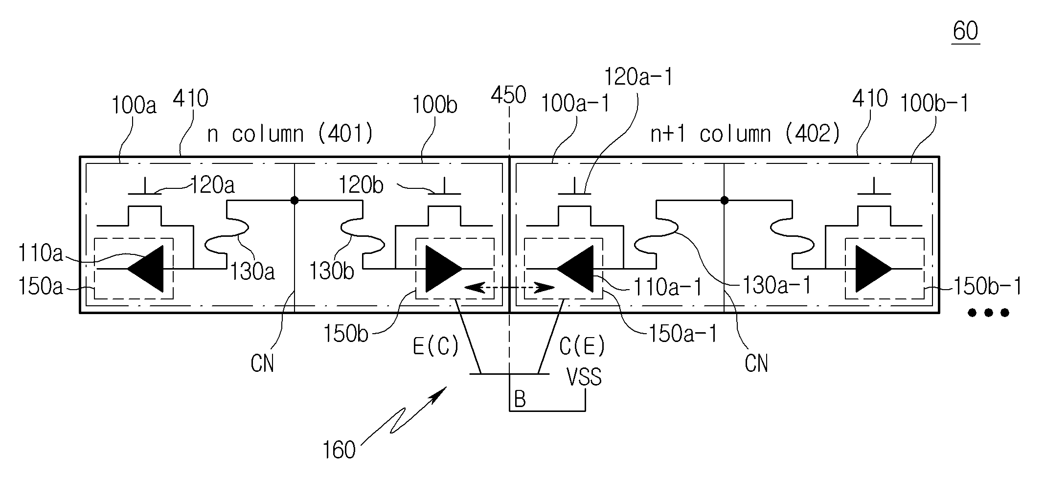
도 4는 일 실시 예에 따른 한 쌍의 단위 셀을 포함하는 퓨즈 타입의 셀 어레이(60)의 구조를 나타내는 예시도이다. FIG. 4 is an exemplary diagram showing the structure of a fuse-type cell array (60) including a pair of unit cells according to one embodiment.
도 4를 참조하면, 퓨즈 타입의 셀 어레이(60)는 적어도 한 쌍의 단위 셀을 포함한다. 적어도 한 쌍의 단위 셀은 제1 단위 셀(100a)과 제2 단위 셀(100b)을 포함할 수 있다. 제1 단위 셀(100a)과 제2 단위 셀(100b)을 각각 짝수(even) 번째 단위 셀(100a)과 홀수(odd) 번째 단위 셀(100b)로 부를 수 있다. 또는 제1 단위 셀(100a)과 제2 단위 셀(100b)을 각각 제1 타입의 단위 셀(100a)과 제2 타입의 단위 셀(100b)로 부를 수 있다. Referring to FIG. 4, the fuse type cell array (60) includes at least one pair of unit cells. The at least one pair of unit cells may include a first unit cell (100a) and a second unit cell (100b). The first unit cell (100a) and the second unit cell (100b) may be referred to as an even unit cell (100a) and an odd unit cell (100b), respectively. Alternatively, the first unit cell (100a) and the second unit cell (100b) may be referred to as a first type unit cell (100a) and a second type unit cell (100b), respectively.
제1 단위 셀(100a)과 제2 단위 셀(100b)은, 공통 노드(CN)를 기준으로 서로 대칭되는 구조를 가질 수 있다. 예를 들어, 제1 단위 셀(100a)은 퓨즈(130a)가 PN 다이오드(110a) 및 제1 NMOS 트랜지스터(120a)의 우측에 배치되는 구조를 갖을 수 있다. 제2 단위 셀(100b)은 퓨즈(130b)가 PN 다이오드(110b) 및 제1 NMOS 트랜지스터(120b)의 좌측에 배치되는 구조를 가질 수 있다. 또한, 제1 단위 셀(100a)과 제2 단위 셀(100b)은 공통 노드(CN)를 기준으로 좌우로 나란히 배치될 수 있다. 예를 들어, 공통 노드(CN)를 기준으로 좌측에 위치한 제1 단위 셀(100a)과 우측에 위치한 제2 단위 셀(100b)이 좌우 대칭 구조를 이루도록, 좌우로 나란한 위치에 배치될 수 있다. 본 문서의 일 실시 예에서는 퓨즈 타입의 셀 어레이(60)의 각 단위 셀들을 상기와 같이 구성함으로써, 퓨즈 타입의 셀 어레이(60)가 차지하는 면적을 최소화할 수 있다. 또한 제1 및 제2 단위 셀을 둘러싸는 P형 가드링(P+ Guard ring, 410)을 배치할 수 있다. P형 가드링(P+ Guard ring, 410)은 고농도로 도핑된 P형 도핑 영역을 말한다. The first unit cell (100a) and the second unit cell (100b) may have a structure that is symmetrical with respect to the common node (CN). For example, the first unit cell (100a) may have a structure in which the fuse (130a) is arranged on the right side of the PN diode (110a) and the first NMOS transistor (120a). The second unit cell (100b) may have a structure in which the fuse (130b) is arranged on the left side of the PN diode (110b) and the first NMOS transistor (120b). In addition, the first unit cell (100a) and the second unit cell (100b) may be arranged side by side to the left and right with respect to the common node (CN). For example, the first unit cell (100a) located on the left side and the second unit cell (100b) located on the right side with respect to the common node (CN) may be arranged in a left-right parallel position to form a left-right symmetrical structure. In one embodiment of this document, by configuring each unit cell of the fuse-type cell array (60) as described above, the area occupied by the fuse-type cell array (60) can be minimized. In addition, a P-type guard ring (P+ Guard ring, 410) surrounding the first and second unit cells can be arranged. The P-type guard ring (P+ Guard ring, 410) refers to a P-type doping region that is heavily doped.
정리해보면, 한 쌍의 단위 셀들은 공통 노드(CN)를 기준으로 서로 대칭되는 구조를 가질 수 있다. 여기서 한 쌍의 단위 셀들은 짝수(even) 번째 단위 셀과 홀수(odd) 번째 단위 셀을 하나씩 포함할 수 있다. 그래서 공통 노드(CN)를 기준으로, 짝수(even) 번째 단위 셀과 홀수(odd) 번째 단위 셀은 서로 대칭되는 구조를 가질 수 있다. 또는 한 쌍의 단위 셀들은 제1 타입의 단위 셀과 제2 타입의 단위 셀을 하나씩 포함할 수 있다. 그래서 공통 노드(CN)를 기준으로, 제1 타입의 단위 셀과 제2 타입의 단위 셀은, 서로 대칭되는 구조를 가질 수 있다.In summary, a pair of unit cells may have a structure that is symmetrical with respect to a common node (CN). Here, a pair of unit cells may include one even unit cell and one odd unit cell. Therefore, with respect to the common node (CN), the even unit cell and the odd unit cell may have a structure that is symmetrical with respect to the common node (CN). Alternatively, a pair of unit cells may include one unit cell of the first type and one unit cell of the second type. Therefore, with respect to the common node (CN), the first type unit cell and the second type unit cell may have a structure that is symmetrical with respect to the common node (CN).
앞서 언급했듯이, 공통 노드(CN)는 공통 라인(common line, CL)으로 부를 수 있다. 공통 라인(common line, CL) 또는 공통 노드(CN)가 프로그램 동작뿐만 아니라, 읽기 동작 시에도 사용될 수 있다. 프로그램 동작 및 읽기 동작에 공통적으로 사용한다는 의미로 공통 노드(CN) 또는 공통 라인(CL)으로 부를 수 있다.As mentioned above, a common node (CN) can be called a common line (CL). A common line (CL) or a common node (CN) can be used not only for program operations but also for read operations. It can be called a common node (CN) or a common line (CL) because it is commonly used for program operations and read operations.
도 5는 일 실시 예에 따른 두 쌍의 단위 셀을 포함하는 퓨즈 타입의 셀 어레이(60)의 구조를 나타내는 예시도이다. FIG. 5 is an exemplary diagram showing the structure of a fuse-type cell array (60) including two pairs of unit cells according to one embodiment.
도 5를 참조하면, 퓨즈 타입의 셀 어레이(60)는 두 쌍의 단위 셀들을 포함할 수 있다. 두 쌍의 단위 셀들 중 한 쌍은 제1 단위 셀(100a), 및 제2 단위 셀(100b)을 포함할 수 있고, 다른 한 쌍은 제3 단위 셀(100a-1)과 제4 단위 셀(100b-1)을 포함할 수 있다. 예를 들어, 퓨즈 타입의 셀 어레이(60)의 n column(401)에는 제1 단위 셀(100a)과 제2 단위 셀(100b)을 포함하는 한 쌍의 단위 셀이 배치될 수 있다. 그리고, 퓨즈 타입의 셀 어레이(60)의 n+1 column(402)에는 제3 단위 셀(100a-1)과 제4 단위 셀(100b-1)을 포함하는 다른 한 쌍의 단위 셀이 배치될 수 있다. 여기서, 제1 단위 셀(100a)과 제4 단위 셀(100b-1)은 서로 미러(mirror) 형태를 갖는다. 마찬가지로, 제2 단위 셀(100b)과 제4 단위 셀(100a-1)도 서로 미러(mirror) 형태를 갖는다. 그래서 n column(401)에 배치된 한 쌍의 단위 셀 구조와, n+1 column(402)에 배치된 다른 한 쌍의 단위 셀 구조는, 제1 가상 선(450)을 기준으로 서로 대칭되는 구조를 가진다. 제1 가상 선(450)은 P형 가드링(410)과 중첩되는 선이다. 그래서 n column(401)에 배치된 한 쌍의 단위 셀 구조와, n+1 column(402)에 배치된 다른 한 쌍의 단위 셀 구조는, P형 가드링(410)를 기준으로 서로 대칭되는 구조를 가진다고 말할 수 있다. Referring to FIG. 5, the fuse type cell array (60) may include two pairs of unit cells. One pair of the two pairs of unit cells may include a first unit cell (100a) and a second unit cell (100b), and the other pair may include a third unit cell (100a-1) and a fourth unit cell (100b-1). For example, a pair of unit cells including a first unit cell (100a) and a second unit cell (100b) may be arranged in the n column (401) of the fuse type cell array (60). And, another pair of unit cells including a third unit cell (100a-1) and a fourth unit cell (100b-1) may be arranged in the n+1 column (402) of the fuse type cell array (60). Here, the first unit cell (100a) and the fourth unit cell (100b-1) have mirror shapes with respect to each other. Similarly, the second unit cell (100b) and the fourth unit cell (100a-1) also have mirror shapes with respect to each other. Therefore, a pair of unit cell structures arranged in the n column (401) and another pair of unit cell structures arranged in the n+1 column (402) have structures that are symmetrical with respect to each other with respect to the first virtual line (450). The first virtual line (450) is a line that overlaps the P-type guard ring (410). Therefore, it can be said that a pair of unit cell structures arranged in the n column (401) and another pair of unit cell structures arranged in the n+1 column (402) have structures that are symmetrical with respect to the P-type guard ring (410).
제1 내지 제4 PN 다이오드(110a, 110b, 110a-1, 110b-1)가 N형 도펀트로 이온 주입된, 제1 내지 제4 NW(N-type Well) 영역들(150a, 150b, 150a-1, 150b-1)에 각각 형성된다. 제2 NW(150b)와 제3 NW(150a-1)은 서로 인접하여 배치된다. 여기서 각 단위 셀들을 상술한 바와 같이 구성하는 경우, 인접한 컬럼들 사이에서 누설 전류(점선의 화살표)가 발생될 수 있다. 예를 들어, PN 다이오드(110)가 형성된 NW(N-type Well) 영역들(150b, 150a-1)이 인접하게 배치되는 경우, 인접한 PN 다이오드 사이에 기생 BJT(parasitic Bipolar Junction Transistor, 160)가 형성되어 누설 전류가 발생될 수 있다. 예를 들어, n번째 행(401)의 1번째 단위 셀(100b) 내 PN 다이오드(110b)와 n+1번째 행(402)의 0번째 단위 셀(100a-1) 내 PN 다이오드(110a-1)가 인접하게 배치되어 두 PN 다이오드들(110b, 110a-1) 사이에 기생 BJT(160)가 형성되어 누설 전류(점선의 화살표)가 발생될 수 있다. PN 다이오드들(110b, 110a-1) 사이에 발생되는 누설 전류(점선의 화살표)는, PN 다이오드들과 전기적으로 연결된 퓨즈를 손상시킬 수 있으므로, 퓨즈의 손상을 방지하기 위해 누설 전류(점선의 화살표)를 최소화하는 것이 매우 중요하다. First to fourth PN diodes (110a, 110b, 110a-1, 110b-1) are formed in first to fourth NW (N-type Well) regions (150a, 150b, 150a-1, 150b-1) that are ion-implanted with N-type dopant, respectively. The second NW (150b) and the third NW (150a-1) are arranged adjacent to each other. Here, when the respective unit cells are configured as described above, a leakage current (dotted arrow) may be generated between adjacent columns. For example, when NW (N-type Well) regions (150b, 150a-1) in which PN diodes (110) are formed are arranged adjacent to each other, a parasitic BJT (parasitic Bipolar Junction Transistor, 160) may be formed between the adjacent PN diodes, causing a leakage current. For example, a PN diode (110b) in the 1st unit cell (100b) of the nth row (401) and a PN diode (110a-1) in the 0th unit cell (100a-1) of the n+1th row (402) may be placed adjacent to each other, so that a parasitic BJT (160) is formed between the two PN diodes (110b, 110a-1), which may cause a leakage current (dotted arrow). The leakage current (dotted arrow) generated between the PN diodes (110b, 110a-1) may damage a fuse electrically connected to the PN diodes, and therefore, it is very important to minimize the leakage current (dotted arrow) in order to prevent damage to the fuse.
따라서, 본 문서의 일 실시 예에서는 인접한 컬럼들 간에 누설 전류가 발생되는 것을 방지하기 위해, 대칭 구조를 갖는 짝수 번째 단위 셀과 홀수 번째 단위 셀 주변에 P형 가드링(P+ Guard ring, 410)을 배치할 수 있다. 예를 들어, n번째 행(401)의 0번째 단위 셀(100a)과 1번째 단위 셀(100b)을 둘러싸는 P형 가드링(410)을 배치하고, n+1번째 행(402)의 0번째 단위 셀(100a-1)과 1번째 단위 셀(100b-1)을 둘러싸는 P형 가드링(410)을 배치할 수 있다. 예컨대, n번째 행(401)의 1번째 단위 셀(100b) 내 PN 다이오드(110b)와 n+1번째 행(402)의 0번째 단위 셀(100a-1) 내 PN 다이오드(110a-1) 사이에는 P형 가드링(410)이 배치됨으로써, 두 PN 다이오드들(110b, 110a-1) 사이에 기생 BJT(160)가 형성되는 것을 방지할 수 있고, 이를 통해 누설 전류(점선의 화살표)가 발생되는 것을 방지할 수 있다. 다시 말해, 두 PN 다이오드들(110b, 110a-1) 사이에 발생하는 누설 전류(점선의 화살표)를 줄이기 위해, 제2 NW(150b)와 제3 NW(150a-1) 사이에 P형 가드링(P+ Guard ring, 410)이 배치될 수 있다. P형 가드링(P+ Guard ring, 410)의 도핑 농도는 제2 NW(150b)와 제3 NW(150a-1)의 도핑 농도보다 높다. Therefore, in one embodiment of the present document, in order to prevent leakage current from occurring between adjacent columns, a P-type guard ring (P+ Guard ring, 410) may be placed around even-numbered unit cells and odd-numbered unit cells having a symmetrical structure. For example, a P-type guard ring (410) may be placed surrounding the 0th unit cell (100a) and the 1st unit cell (100b) of the nth row (401), and a P-type guard ring (410) may be placed surrounding the 0th unit cell (100a-1) and the 1st unit cell (100b-1) of the n+1th row (402). For example, a P-type guard ring (410) is arranged between the PN diode (110b) in the 1st unit cell (100b) of the nth row (401) and the PN diode (110a-1) in the 0th unit cell (100a-1) of the n+1th row (402), thereby preventing a parasitic BJT (160) from being formed between the two PN diodes (110b, 110a-1), and thereby preventing a leakage current (dotted arrow) from being generated. In other words, a P-type guard ring (P+ Guard ring, 410) may be arranged between the second NW (150b) and the third NW (150a-1) in order to reduce the leakage current (dotted arrow) generated between the two PN diodes (110b, 110a-1). The doping concentration of the P-type guard ring (P+ guard ring, 410) is higher than the doping concentrations of the second NW (150b) and the third NW (150a-1).
도 6a는 일 실시 예에 따른 4 쌍의 단위 셀을 포함하는 퓨즈 타입의 셀 어레이(60)의 구조를 나타내는 예시도이다. FIG. 6a is an exemplary diagram showing the structure of a fuse-type cell array (60) including four pairs of unit cells according to one embodiment.
도 6a를 참조하면, 퓨즈 타입의 셀 어레이(60)의 first row에는 적어도 4개의 단위 셀들(100a, 100b, 100a-1, 100b-1)을 포함하고 있다. 또한 second row에는 적어도 4개의 단위 셀들(100c, 100d, 100c-1, 100d-1)을 포함하고 있다. Referring to FIG. 6a, the first row of the fuse type cell array (60) includes at least four unit cells (100a, 100b, 100a-1, 100b-1). Additionally, the second row includes at least four unit cells (100c, 100d, 100c-1, 100d-1).
퓨즈 타입의 셀 어레이(60)에서 한 쌍의 단위 셀 구조는 도 4에서 설명한 바와 같다. 즉, 한 쌍의 단위 셀들은 공통 노드(CN)를 기준으로 서로 대칭되는 구조를 가질 수 있다. 여기서 한 쌍의 단위 셀들은 짝수(even) 번째 단위 셀과 홀수(odd) 번째 단위 셀을 하나씩 포함할 수 있다. 그래서 공통 노드(CN)를 기준으로, 짝수(even) 번째 단위 셀과 홀수(odd) 번째 단위 셀은 서로 대칭되는 구조를 가질 수 있다. 또는 한 쌍의 단위 셀들은 제1 타입의 단위 셀과 제2 타입의 단위 셀을 하나씩 포함할 수 있다. 그래서 공통 노드(CN)를 기준으로, 제1 타입의 단위 셀과 제2 타입의 단위 셀은, 서로 대칭되는 구조를 가질 수 있다.The structure of a pair of unit cells in the fuse type cell array (60) is as described in FIG. 4. That is, a pair of unit cells may have a structure that is symmetrical with respect to a common node (CN). Here, a pair of unit cells may include an even unit cell and an odd unit cell, respectively. Therefore, with respect to the common node (CN), the even unit cell and the odd unit cell may have a structure that is symmetrical with respect to the common node (CN). Alternatively, a pair of unit cells may include a first type unit cell and a second type unit cell, respectively. Therefore, with respect to the common node (CN), the first type unit cell and the second type unit cell may have a structure that is symmetrical with respect to the common node (CN).
예를 들어, 각 행(column)(401, 402)의 짝수(even) 번째 단위 셀들(100a, 100c)(또는 제1 타입 단위 셀들)과 홀수(odd) 번째 단위 셀들(100b, 100d)(또는 제2 타입 단위 셀들)은, 공통 노드(CN)를 기준으로 서로 대칭되는 구조를 가질 수 있다. 예를 들어, 0번째 단위 셀(100a)은 퓨즈(130a)가 PN 다이오드(110a) 및 제1 NMOS 트랜지스터(120a)의 우측에 배치되는 구조를 갖고, 1번째 단위 셀(100b)은 퓨즈(130b)가 PN 다이오드(110b) 및 제1 NMOS 트랜지스터(120b)의 좌측에 배치되는 구조를 가질 수 있다. 또한, 짝수(even) 번째 단위 셀들(100a, 100c)과 홀수(odd) 번째 단위 셀들(100b, 100d)은 공통 노드(CN)를 기준으로 좌우로 나란히 배치될 수 있다. 예를 들어, 공통 노드(CN)를 기준으로 좌측에 위치한 0번째 단위 셀(100a)과 우측에 위치한 1번째 단위 셀(100b)이 좌우 대칭 구조를 이루도록, 좌우로 나란한 위치에 배치될 수 있다. 본 문서의 일 실시 예에서는 퓨즈 타입의 셀 어레이(60)의 각 단위 셀들을 상기와 같이 구성함으로써, 퓨즈 타입의 셀 어레이(60)가 차지하는 면적을 최소화할 수 있다.For example, the even unit cells (100a, 100c) (or the first type unit cells) and the odd unit cells (100b, 100d) (or the second type unit cells) of each row (column) (401, 402) may have structures that are symmetrical with respect to a common node (CN). For example, the 0th unit cell (100a) may have a structure in which a fuse (130a) is arranged on the right side of a PN diode (110a) and a first NMOS transistor (120a), and the 1st unit cell (100b) may have a structure in which a fuse (130b) is arranged on the left side of a PN diode (110b) and a first NMOS transistor (120b). In addition, the even-numbered unit cells (100a, 100c) and the odd-numbered unit cells (100b, 100d) may be arranged side by side on the left and right with respect to the common node (CN). For example, the 0th unit cell (100a) located on the left and the 1st unit cell (100b) located on the right with respect to the common node (CN) may be arranged in a side by side position to form a left-right symmetrical structure. In one embodiment of the present document, by configuring each unit cell of the fuse-type cell array (60) as described above, the area occupied by the fuse-type cell array (60) may be minimized.
계속해서, 도 6a를 참조하면, 퓨즈 타입의 셀 어레이(60)에서 first row에 있는 단위 셀들의 구조(100a, 100b, 100a-1, 100b-1)는 앞서 도 5에서 설명한 바와 같다. 즉, n column(401)에 배치된 한 쌍의 단위 셀(100a, 100b) 구조와, n+1 column(402)에 배치된 다른 한 쌍의 단위 셀(100a-1, 100b-1) 구조는, P형 가드링(410)를 기준으로 서로 대칭되는 구조를 가진다고 말할 수 있다. Continuing, referring to FIG. 6a, the structure (100a, 100b, 100a-1, 100b-1) of the unit cells in the first row in the fuse type cell array (60) is as described above in FIG. 5. That is, it can be said that the structure of a pair of unit cells (100a, 100b) arranged in an n column (401) and the structure of another pair of unit cells (100a-1, 100b-1) arranged in an n+1 column (402) have structures that are symmetrical with respect to the P-type guard ring (410).
또한, 가상 선(450)을 기준으로, n column(401)에 배치된 단위 셀들(100a, 100b, 100c, 100d) 구조는, n+1 column(402)에 배치된 단위 셀들(100a-1, 100b-1, 100c-1, 100d-1) 구조와 서로 대칭되는 구조(mirror 형태)를 가진다. 여기서 가상 선(450)은 P형 가드링(410)과 중첩되는 선이다. 다른 말로 표현하면, P형 가드링(410)을 기준으로, n column(401)에 배치된 단위 셀들(100a, 100b, 100c, 100d) 구조는, n+1 column(402)에 배치된 단위 셀들(100a-1, 100b-1, 100c-1, 100d-1) 구조와 서로 대칭되는 구조(mirror 형태)를 가진다. In addition, based on the virtual line (450), the structure of the unit cells (100a, 100b, 100c, 100d) arranged in the n column (401) has a structure (mirror form) that is symmetrical to the structure of the unit cells (100a-1, 100b-1, 100c-1, 100d-1) arranged in the n+1 column (402). Here, the virtual line (450) is a line that overlaps the P-type guard ring (410). In other words, with respect to the P-type guard ring (410), the structure of unit cells (100a, 100b, 100c, 100d) arranged in n column (401) has a structure (mirror form) that is symmetrical to the structure of unit cells (100a-1, 100b-1, 100c-1, 100d-1) arranged in n+1 column (402).
계속해서, 도 6a를 참조하면, second row에 있는 단위 셀들(100c, 100d, 100c-1, 100d-1)은 first row에 있는 단위 셀들(100a, 100b, 100a-1, 100b-1)과 똑같은 모양으로 반복되는 구조를 갖는다. 그리고 PN 다이오드 위치가 가급적 서로 멀리 떨어져 있는 구조이다. First row에 배치된 PN 다이오드와 second row에 PN 다이오드는 최대한 멀리 떨어져 배치된다. First row에 있는 단위 셀들(100a, 100b, 100a-1, 100b-1)과 second row에 있는 단위 셀들(100c, 100d, 100c-1, 100d-1) 사이에는 누설 전류를 줄이기 위한, P형 가드링 구조(410)가 형성되어 있다. Continuing, referring to FIG. 6a, the unit cells (100c, 100d, 100c-1, 100d-1) in the second row have a structure that is repeated in the same shape as the unit cells (100a, 100b, 100a-1, 100b-1) in the first row. And the PN diode positions are structured to be as far apart from each other as possible. The PN diodes arranged in the first row and the PN diodes in the second row are arranged as far apart as possible. A P-type guard ring structure (410) is formed between the unit cells (100a, 100b, 100a-1, 100b-1) in the first row and the unit cells (100c, 100d, 100c-1, 100d-1) in the second row to reduce leakage current.
도 6b는 일 실시 예에 따른 4 쌍의 단위 셀을 포함하는 퓨즈 타입의 셀 어레이(60)의 구조를 나타내는 예시도이다. FIG. 6b is an exemplary diagram showing the structure of a fuse-type cell array (60) including four pairs of unit cells according to one embodiment.
도 6b를 참조하면, 퓨즈 타입의 셀 어레이(60)에서 first row에 있는 단위 셀들의 구조(100a, 100b, 100a-1, 100b-1)는 앞서 도 5에서 설명한 바와 같다. 그런데 n column(401) 및 second row에 있는 단위 셀들(100c, 100d)은, 제2 가상 선(470)을 기준으로 first row에 있는 단위 셀들(100a, 100b)의 구조와 mirror 형태를 갖는다. 마찬가지로 n+1 column(402) 및 second row에 있는 단위 셀들(100c-1, 100d-1)도 first row 에 있는 단위 셀들(100a-1, 100b-1)과 제2 가상 선(470)을 기준으로 mirror 형태를 갖는다. 그래서 제1 가상 선(450)과 제2 가상 선(470)이 교차되는 중앙 부분에 4개의 PN 다이오드들(110b, 110a-1, 110d, 110c-1)이 서로 가까이 배치되는 모양을 갖는다. 4개의 PN 다이오드들(110b, 110a-1, 110d, 110c-1)이 서로 가까이 배치되어도 고농도의 P형 가드링(410)이 그 PN 다이오드들(110b, 110a-1, 110d, 110c-1) 사이에 배치되어 있기 때문에, 누설 전류를 막을 수 있다. Referring to FIG. 6b, the structure (100a, 100b, 100a-1, 100b-1) of the unit cells in the first row in the fuse type cell array (60) is as described above in FIG. 5. However, the unit cells (100c, 100d) in the n column (401) and the second row have a mirror shape with respect to the structure of the unit cells (100a, 100b) in the first row with respect to the second virtual line (470). Similarly, the unit cells (100c-1, 100d-1) in the n+1 column (402) and the second row also have a mirror shape with respect to the unit cells (100a-1, 100b-1) in the first row with respect to the second virtual line (470). Therefore, four PN diodes (110b, 110a-1, 110d, 110c-1) are arranged close to each other in the central portion where the first virtual line (450) and the second virtual line (470) intersect. Even if the four PN diodes (110b, 110a-1, 110d, 110c-1) are arranged close to each other, leakage current can be prevented because a high-concentration P-type guard ring (410) is arranged between the PN diodes (110b, 110a-1, 110d, 110c-1).
본 문서의 실시 예들에 따르면, 이퓨즈 셀 어레이를 도 4, 도 5, 도 6a 및 도6b에 도시된 바와 같이 구성함으로써, 이퓨즈 셀 어레이의 면적을 최소화하면서, 누설 전류가 발생되는 것을 방지할 수 있다.According to embodiments of the present document, by configuring the e-fuse cell array as illustrated in FIGS. 4, 5, 6a, and 6b, the area of the e-fuse cell array can be minimized while preventing leakage current from occurring.
도 7은 다양한 실시 예들에 따른 퓨즈 타입 셀 어레이를 갖는 비휘발성 메모리 장치에서 단위 셀의 연결 구조를 나타내는 도면이다.FIG. 7 is a diagram showing a connection structure of a unit cell in a nonvolatile memory device having a fuse type cell array according to various embodiments.
도 7을 참조하면, 단위 셀(100)은 PN 다이오드(110), 제1 NMOS 트랜지스터(또는 제1 스위칭 소자)(120) 및 퓨즈(130)를 포함할 수 있다. 단위 셀(100) 내부의 다이오드(110), 제1 NMOS 트랜지스터(120), 및 퓨즈(130)의 연결 구조는 도 3에서 설명한 바와 동일하므로, 이에 대한 설명은 생략한다. Referring to FIG. 7, the unit cell (100) may include a PN diode (110), a first NMOS transistor (or a first switching element) (120), and a fuse (130). The connection structure of the diode (110), the first NMOS transistor (120), and the fuse (130) inside the unit cell (100) is the same as described in FIG. 3, and therefore, a description thereof is omitted.
일 실시 예에 따르면, 단위 셀(100)의 퓨즈(130)는 공통 노드(CN)를 통해 단위 셀 외부에 배치된 제2 NMOS 트랜지스터(또는 제2 스위칭 소자)(140), 및 제1 PMOS 트랜지스터(또는 제3 스위칭 소자)(210)와 연결될 수 있다. 여기서, 제2 및 제3 스위칭 소자들(140, 210)은 단위 셀(100)의 외부에 배치될 수 있다. 이는, 제2 및 제3 스위칭 소자들(140, 210)이 동일 행에 포함되는 복수의 단위 셀들에 공통으로 연결되기 때문이다. 예를 들어, 제2 NMOS 트랜지스터(140) 및 제1 PMOS 트랜지스터(210)는 공통 노드(CN)를 통해 n번째 행에 포함되는 복수의 단위 셀들과 연결될 수 있다. According to one embodiment, the fuse (130) of the unit cell (100) may be connected to a second NMOS transistor (or second switching element) (140) and a first PMOS transistor (or third switching element) (210) disposed outside the unit cell through a common node (CN). Here, the second and third switching elements (140, 210) may be disposed outside the unit cell (100). This is because the second and third switching elements (140, 210) are commonly connected to a plurality of unit cells included in the same row. For example, the second NMOS transistor (140) and the first PMOS transistor (210) may be connected to a plurality of unit cells included in the nth row through the common node (CN).
상술한 바와 같이, 제2 및 제3 스위칭 소자들(140, 210)을 단위 셀(100) 외부에 배치함으로써, 각 단위 셀(100)의 크기를 최소화하여, 복수의 단위 셀들로 구성된 이퓨즈 셀 어레이(60) 전체의 크기를 감소시킬 수 있다. 즉, 비휘발성 메모리 장치(10)의 칩의 면적 중 가장 많은 면적을 차지하는 이퓨즈 셀 어레이(60)의 크기를 감소시킴으로써, 칩의 크기를 축소시킬 수 있는 효과를 얻을 수 있다.As described above, by arranging the second and third switching elements (140, 210) outside the unit cell (100), the size of each unit cell (100) can be minimized, thereby reducing the size of the entire e-fuse cell array (60) composed of a plurality of unit cells. That is, by reducing the size of the e-fuse cell array (60) that occupies the largest area among the areas of the chip of the nonvolatile memory device (10), the effect of reducing the size of the chip can be obtained.
제2 NMOS 트랜지스터(140)의 게이트 단자는 RD와 연결되고, 양단은 공통 노드(CN) 및 접지와 연결될 수 있다. 예를 들어, 제2 NMOS 트랜지스터(140)는 공통 노드(CN)를 통해 복수의 단위 셀들의 퓨즈들과 연결될 수 있다.The gate terminal of the second NMOS transistor (140) is connected to RD, and both ends can be connected to a common node (CN) and ground. For example, the second NMOS transistor (140) can be connected to fuses of a plurality of unit cells through the common node (CN).
제1 PMOS 트랜지스터(210)의 게이트 단자는 BLOWB 라인과 연결되고, 양단은 전원 전압 및 공통 노드(CN)에 연결될 수 있다. 예를 들어, 제1 PMOS 트랜지스터(210)는 공통 노드(CN)를 통해 복수의 단위 셀들의 퓨즈들과 연결될 수 있다. BLOWB 라인은, 퓨즈 블로잉(fuse blowing) 여부를 나타내는 신호에 대한 반전 신호가 제공되는 라인일 수 있다.The gate terminal of the first PMOS transistor (210) is connected to the BLOWB line, and both ends can be connected to a power supply voltage and a common node (CN). For example, the first PMOS transistor (210) can be connected to fuses of a plurality of unit cells through the common node (CN). The BLOWB line can be a line to which an inverted signal for a signal indicating whether a fuse is blowing is provided.
도 8은 다양한 실시 예들에 따른 단위 셀의 읽기 전류 및 쓰기 전류 흐름을 나타내는 예시도이다.FIG. 8 is an exemplary diagram showing read current and write current flows of a unit cell according to various embodiments.
도 8을 참조하면, 점선 화살표 ①은 프로그램 동작 시의 단위 셀(100)에 대한 전류 흐름 경로를 나타낸다. Referring to Figure 8, the dotted
일 실시 예에 따르면, 제1 PMOS 트랜지스터(210)는 BLOWB 라인을 통해 하이 레벨의 신호가 제공되는 경우에 오프(OFF)될 수 있다. 여기서, 하이 레벨의 BLOWB는 퓨즈 블로잉이 필요하지 않음을 나타낼 수 있다.According to one embodiment, the first PMOS transistor (210) may be turned off when a high level signal is provided through the BLOWB line. Here, a high level of BLOWB may indicate that fuse blowing is not required.
일 실시 예에 따르면, 제1 PMOS 트랜지스터(210)는 BLOWB 라인을 통해 로우 레벨의 신호가 제공되는 경우, 온(ON)되어 프로그램 전압에 따른 프로그램 전류를 공통 노드(CN)로 제공할 수 있다. 여기서, 로우 레벨의 BLOWB는 데이터 '1'의 프로그래밍을 위해 퓨즈 블로잉이 필요함을 나타낼 수 있다. 프로그램 전류는 공통 노드(CN)를 통해 퓨즈(130)에 전달되며, 퓨즈(130)는 프로그램 전류에 의해 프로그래밍 또는 블로잉 될 수 있다. 프로그래밍 또는 블로잉은 퓨즈의 저항을 올리는 작업을 의미한다. 프로그램 전류는 퓨즈(130)의 애노드에서 캐소드 방향으로 흐르며, PN 다이오드(110)를 통해 WWLB로 빠져나갈 수 있다. 여기서, WWLB는 미리 선택되어 있어야 한다.According to one embodiment, when a low-level signal is provided through the BLOWB line, the first PMOS transistor (210) may be turned on to provide a program current according to a program voltage to the common node (CN). Here, the low-level BLOWB may indicate that fuse blowing is required for programming data '1'. The program current is transmitted to the fuse (130) through the common node (CN), and the fuse (130) may be programmed or blown by the program current. Programming or blowing means an operation of increasing the resistance of the fuse. The program current flows from the anode to the cathode of the fuse (130) and may escape to the WWLB through the PN diode (110). Here, the WWLB must be selected in advance.
도 8을 참조하면, 점선 화살표 ②는 읽기 동작 시의 단위 셀(100)에 대한 전류 흐름 경로를 나타낸다. Referring to Fig. 8, the dotted
일 실시 예에 따르면, 제1 NMOS 트랜지스터(120)는 RWL 라인을 통해 게이트에 로우 레벨의 신호가 제공되는 경우에 오프(OFF)되고, RWL 라인을 통해 게이트에 하이 레벨의 신호가 제공되는 경우에 온(ON)될 수 있다. 여기서, 로우 레벨의 RWL 신호는 해당 읽기 워드 라인이 선택되지 않았음을 나타낼 수 있고, 하이 레벨의 RWL 신호는 해당 읽기 워드 라인이 선택되었음을 나타낼 수 있다. According to one embodiment, the first NMOS transistor (120) may be turned off when a low-level signal is provided to the gate through the RWL line, and may be turned on when a high-level signal is provided to the gate through the RWL line. Here, a low-level RWL signal may indicate that a corresponding read word line is not selected, and a high-level RWL signal may indicate that a corresponding read word line is selected.
일 실시 예에 따르면, 제2 NMOS 트랜지스터(140)는 RD 라인을 통해 게이트에 로우 레벨의 신호가 제공되는 경우에 오프(OFF)되고, RD 라인을 통해 게이트에 하이 레벨의 신호가 제공되는 경우에 온(ON)될 수 있다. 여기서, 하이 레벨의 RD는 읽기 모드를 나타내고, 로우 레벨의 RD는 읽기 모드가 아님을 나타낼 수 있다.According to one embodiment, the second NMOS transistor (140) may be turned off when a low-level signal is provided to the gate through the RD line, and may be turned on when a high-level signal is provided to the gate through the RD line. Here, a high-level RD may indicate a read mode, and a low-level RD may indicate a non-read mode.
일 실시 예에 따르면, 제1 NMOS 트랜지스터(120)와 제2 NMOS 트랜지스터(140)가 모두 온 된 경우, 제1 NMOS 트랜지스터(120)는 비트 라인(BL)으로부터 제공되는 읽기 전압에 따라 읽기 전류를 퓨즈(130)에 인가할 수 있다. 읽기 전류는 퓨즈(130)를 통과할 수 있으며, 읽기 전류의 값은 퓨즈(130)의 저항에 따라 달라질 수 있다. 예를 들어, 퓨즈(130)가 블로잉 된 경우의 읽기 전류의 값은 퓨즈(130)가 블로잉 되지 않은 경우의 읽기 전류의 값보다 작을 수 있다. 퓨즈(130)를 통과한 읽기 전류는 공통 노드(CN)를 통해 제2 NMOS 트랜지스터(140)로 흐를 수 있다. 여기서 읽기 전류는 퓨즈(130)의 캐소드에서 애노드 방향으로 흐르는 바, 읽기 전류의 방향은 프로그램 전류와는 반대방향으로 흐른다고 볼 수 있다. 또한, 읽기 전류는 PN 다이오드(110)를 통과하지 않기 때문에, 읽기 동작을 위해 높은 구동 전압이 사용되지 않아도 된다. 따라서 읽기 전류는 낮은 구동 전류를 사용할 수 있다. 읽기 전류의 값은 퓨즈(130)가 프로그램 되었는지 여부를 체크하는데 이용될 수 있다.According to one embodiment, when both the first NMOS transistor (120) and the second NMOS transistor (140) are turned on, the first NMOS transistor (120) can apply a read current to the fuse (130) according to a read voltage provided from the bit line (BL). The read current can pass through the fuse (130), and the value of the read current can vary depending on the resistance of the fuse (130). For example, the value of the read current when the fuse (130) is blown can be smaller than the value of the read current when the fuse (130) is not blown. The read current passing through the fuse (130) can flow to the second NMOS transistor (140) through the common node (CN). Here, the read current flows from the cathode to the anode of the fuse (130), and the direction of the read current can be regarded as flowing in the opposite direction to the program current. In addition, since the read current does not pass through the PN diode (110), a high driving voltage does not need to be used for the read operation. Therefore, the read current can use a low driving current. The value of the read current can be used to check whether the fuse (130) is programmed.
본 문서의 다양한 실시 예들에 따른 퓨즈 타입 셀 어레이를 갖는 비휘발성 메모리 장치(10)는 제1 단위 셀에 고전압을 인가하여 퓨즈를 끊음으로써, 제1 단위 셀에 데이터 '1'을 프로그램하거나, 제1 단위 셀에 고전압을 인가하지 않고 퓨즈를 끊어지지 않은 상태로 유지함으로써, 제1 단위 셀에 데이터 '0'을 프로그램 할 수 있다. 비휘발성 메모리 장치(10)에서 제1 단위 셀에 데이터 '1'을 프로그램하는 경우, 제1 단위 셀에 인가된 고전압 의해 공통 노드(CN)에 전압이 충전될 수 있다. 공통 노드(CN)에는 복수의 단위 셀들이 연결되어 있으므로, 제1 단위 셀의 프로그램 시에 공통 노드(CN)에 충전된 전압은 다른 단위 셀의 퓨즈를 손상시킬 수 있다. 예를 들어, 제2 단위 셀에 데이터 '0'을 프로그램 해야 하는 상황에서, 공통 노드에 충전된 전압에 의해 제2 단위 셀의 퓨즈가 끊어져 제2 단위 셀에 데이터 '1'이 프로그램되는 것과 같은 상황이 발생될 수 있다.A nonvolatile memory device (10) having a fuse type cell array according to various embodiments of the present document can program data '1' in a first unit cell by applying a high voltage to the first unit cell to blow the fuse, or can program data '0' in the first unit cell by not applying a high voltage to the first unit cell and keeping the fuse unblown. When programming data '1' in the first unit cell in the nonvolatile memory device (10), a voltage may be charged in a common node (CN) by the high voltage applied to the first unit cell. Since a plurality of unit cells are connected to the common node (CN), the voltage charged in the common node (CN) when programming the first unit cell may damage the fuse of another unit cell. For example, in a situation where data '0' should be programmed in a second unit cell, a situation may occur where the fuse of the second unit cell is blown by the voltage charged in the common node, thereby programming data '1' in the second unit cell.
따라서, 본 문서의 다양한 실시 예들에서는 프로그램 동작에 의해 공통 노드에 충전된 전압을 방전하는 회로 구조를 개시한다.Therefore, various embodiments of the present document disclose a circuit structure for discharging a voltage charged to a common node by a program operation.
도 9는 다양한 실시 예들에 따른 퓨즈 타입 셀 어레이를 갖는 비휘발성 메모리 장치에서 공통 노드에 대한 방전 회로 구성도이다. FIG. 9 is a diagram of a discharge circuit configuration for a common node in a nonvolatile memory device having a fuse type cell array according to various embodiments.
도 9를 참조하면, 비휘발성 메모리 장치(10)는 공통 노드 방전 회로(710)를 더 포함할 수 있다. 일 실시 예에 따르면, 비휘발성 메모리 장치(10)는, 도 1 내지 도 8에서 설명된 구성 요소들(예: 제어 로직(20), 워드 라인 드라이버(40), 프로그래밍 드라이버(50), 이퓨즈 셀 어레이(60), 및 비트 라인 센스 앰프(70)) 이외에 각 행에 연결된 공통 노드 방전 회로(710)를 더 포함할 수 있다. Referring to FIG. 9, the nonvolatile memory device (10) may further include a common node discharge circuit (710). According to one embodiment, the nonvolatile memory device (10) may further include a common node discharge circuit (710) connected to each row in addition to the components described in FIGS. 1 to 8 (e.g., control logic (20), word line driver (40), programming driver (50), e-fuse cell array (60), and bit line sense amplifier (70)).
일 실시 예에 따르면, 공통 노드 방전 회로(710)는 단위 셀(100)의 주변 영역에 배치될 수 있다. 예를 들어, 공통 노드 방전 회로(710)는 제2 NMOS 트랜지스터(140) 및 제1 PMOS 트랜지스터(210)와 같이, 단위 셀(100) 외부에 배치될 수 있다. 이는, 공통 노드 방전 회로(710)가 공통 노드(CN)를 통해 복수의 단위 셀들에 연결되기 때문이다. 즉, 도시의 편의를 위해 도 9에는 하나의 단위 셀(100)만을 도시하였으나, 공통 노드 방전 회로(710)는 하나의 공통 노드(CN)를 통해 n번째 행에 포함되는 복수의 단위 셀들과 공통으로 연결될 수 있다. 따라서, 본 문서의 실시 예들에서는 공통 노드 방전 회로(710)를 단위 셀(100)의 주변 영역에 배치함으로써, 단위 셀(100) 및 이퓨즈 셀 어레이(60)의 크기를 최소화할 수 있다. According to one embodiment, the common node discharge circuit (710) may be arranged in a peripheral area of the unit cell (100). For example, the common node discharge circuit (710) may be arranged outside the unit cell (100), such as the second NMOS transistor (140) and the first PMOS transistor (210). This is because the common node discharge circuit (710) is connected to a plurality of unit cells through the common node (CN). That is, for convenience of illustration, only one unit cell (100) is illustrated in FIG. 9, but the common node discharge circuit (710) may be commonly connected to a plurality of unit cells included in the nth row through one common node (CN). Therefore, in the embodiments of the present document, by arranging the common node discharge circuit (710) in a peripheral area of the unit cell (100), the sizes of the unit cell (100) and the e-fuse cell array (60) may be minimized.
공통 노드 방전 회로(710)는 공통 노드에 충전된 전압에 의해 공통 노드에 연결된 단위 셀들의 퓨즈가 손상되는 것을 방지하기 위한 회로로, 공통 노드에 충전된 전압을 RD 신호 및 BLOWB 신호에 따라 방전할 수 있다. The common node discharge circuit (710) is a circuit to prevent the fuses of unit cells connected to the common node from being damaged by the voltage charged to the common node, and can discharge the voltage charged to the common node according to the RD signal and the BLOWB signal.
공통 노드 방전 회로(710)는 제1 인버터(또는 제1 NOT 게이트, 717), 제1 NAND 게이트(711), 제2 인버터(또는 제2 NOT 게이트, 713), 및 제3 NMOS 트랜지스터(715)를 포함할 수 있다.The common node discharge circuit (710) may include a first inverter (or a first NOT gate, 717), a first NAND gate (711), a second inverter (or a second NOT gate, 713), and a third NMOS transistor (715).
제1 인버터(717)는 제2 NMOS 트랜지스터(140)와 비트 라인 센스 앰프(70) 사이의 제2 노드(N2)와 제1 NAND 게이트(711)에 연결될 수 있다. 제1 인버터(717)는 비트 라인 센스 앰프(70)로부터 제공되는 RD 신호를 반전시켜 제1 NAND 게이트(711)로 출력할 수 있다. RD 신호는 읽기 모드 여부를 나타내는 신호일 수 있다. 예를 들어, 하이 레벨의 RD 신호는 읽기 모드를 나타내고, 로우 레벨의 RD 신호는 읽기 모드가 아님을 나타낼 수 있다.A first inverter (717) may be connected to a second node (N2) between a second NMOS transistor (140) and a bit line sense amplifier (70) and a first NAND gate (711). The first inverter (717) may invert an RD signal provided from the bit line sense amplifier (70) and output the inverted signal to the first NAND gate (711). The RD signal may be a signal indicating whether or not a read mode is in effect. For example, a high level RD signal may indicate a read mode, and a low level RD signal may indicate that the mode is not in effect.
제1 NAND 게이트(711)의 입력 단들은 프로그래밍 드라이버(50)의 BLOWB 라인과 제1 인버터(717)에 연결되고, 출력 단은 제2 인버터(713)에 연결될 수 있다. 제1 NAND 게이트(711)는 프로그래밍 드라이버(50)로부터 제공되는 BLOWB 신호와 제1 인버터(717)로부터 제공되는 신호에 대한 부정 논리곱 연산을 수행하고, 그 결과를 출력할 수 있다. BLOWB 신호는 퓨즈 블로잉 여부를 나타내는 신호에 대한 반전 신호를 의미할 수 있다. 예를 들어, 로우 레벨의 BLOWB 신호는 퓨즈 블로잉(blowing)이 필요함을 나타내는 신호이고, 하이 레벨의 BLOWB 신호는 퓨즈 블로잉이 필요하지 않음을 나타내는 신호일 수 있다. The input terminals of the first NAND gate (711) may be connected to the BLOWB line of the programming driver (50) and the first inverter (717), and the output terminal may be connected to the second inverter (713). The first NAND gate (711) may perform a negative AND operation on the BLOWB signal provided from the programming driver (50) and the signal provided from the first inverter (717), and output the result. The BLOWB signal may mean an inverted signal for a signal indicating whether a fuse is blown. For example, a BLOWB signal at a low level may be a signal indicating that fuse blowing is necessary, and a BLOWB signal at a high level may be a signal indicating that fuse blowing is not necessary.
제2 인버터(713)는 제1 NAND 게이트(711)의 출력 단과 제3 NMOS 트랜지스터(715)의 게이트에 연결될 수 있다. 제2 인버터(713)는 제1 NAND 게이트(711)로부터 제공되는 신호를 반전시켜 제3 NMOS 트랜지스터(715)의 게이트로 제공할 수 있다.The second inverter (713) can be connected to the output terminal of the first NAND gate (711) and the gate of the third NMOS transistor (715). The second inverter (713) can invert the signal provided from the first NAND gate (711) and provide it to the gate of the third NMOS transistor (715).
제3 NMOS 트랜지스터(715)는 공통 노드(CN)와 프로그래밍 드라이버(50) 사이의 제3 노드(N3)와 접지에 연결될 수 있다. 제3 NMOS 트랜지스터(715)는 게이트에 하이 레벨의 신호가 입력되는 경우, 온(ON)되어 제3 노드(N3)를 통해 공통 노드(CN)에 충전된 전압을 방전 시킬 수 있다. The third NMOS transistor (715) can be connected to the third node (N3) between the common node (CN) and the programming driver (50) and the ground. When a high level signal is input to the gate, the third NMOS transistor (715) can be turned on and discharge the voltage charged to the common node (CN) through the third node (N3).
단위 셀(100)의 구성, 및 다른 구성 요소들과의 연결 구조는 도 3 내지 도 7에서 설명한 바와 동일하며, 단위 셀(100)의 동작은 도 8에서 설명한 바와 같다. 따라서, 단위 셀(100)의 구성, 연결 구조, 및 동작에 대한 설명은 생략할 것이다.The configuration of the unit cell (100) and the connection structure with other components are the same as described in FIGS. 3 to 7, and the operation of the unit cell (100) is the same as described in FIG. 8. Therefore, the description of the configuration, connection structure, and operation of the unit cell (100) will be omitted.
프로그래밍 드라이버(50)는 제어 로직(20)의 제어 신호에 따라 프로그램 전압을 생성하고 이퓨즈 셀 어레이(60)의 특정 행을 선택할 수 있다. 프로그래밍 드라이버(50)는 생성된 프로그램 전압을 선택된 행의 공통 노드(CN)로 제공할 수 있다. 일 실시 예에 따르면, 프로그래밍 드라이버(50)는 도 7에 도시된 바와 같은 제1 PMOS 트랜지스터(210)를 포함할 수 있다. 예를 들어, 프로그래밍 드라이버(50)는 이퓨즈 셀 어레이(60)의 각 행들의 공통 노드(CN)에 연결된 복수의 제1 PMOS 트랜지스터들을 포함할 수 있다. The programming driver (50) can generate a program voltage according to a control signal of the control logic (20) and select a specific row of the e-fuse cell array (60). The programming driver (50) can provide the generated program voltage to a common node (CN) of the selected row. According to one embodiment, the programming driver (50) can include a first PMOS transistor (210) as illustrated in FIG. 7. For example, the programming driver (50) can include a plurality of first PMOS transistors connected to the common node (CN) of each row of the e-fuse cell array (60).
일 실시 예에 따르면, 프로그래밍 드라이버(50)는 제어 로직(20)의 제어 신호에 따라 BLOWB 신호를 공통 노드 방전 회로(710)의 제1 NAND 게이트(711)로 제공할 수 있다. BLOWB 신호는, 특정 단위 셀(100)에 대한 퓨즈 블로잉이 필요한 경우에만 로우 레벨로 출력되고, 그 이외의 경우에는 하이 레벨로 출력될 수 있다. 예를 들어, 특정 단위 셀(100)에 데이터 '1'을 프로그램하기 위한 모드인 경우, 퓨즈 블로잉이 필요하므로 프로그래밍 드라이버(50)는 제어 로직(20)의 제어에 따라 로우 레벨의 BLOWB 신호를 출력할 수 있다. 다른 예로, 특정 단위 셀(100)에 데이터 '0'을 프로그램하기 위한 모드인 경우, 퓨즈 블로잉이 필요하지 않으므로 프로그래밍 드라이버(50)는 제어 로직(20)의 제어에 따라 하이 레벨의 BLOWB 신호를 출력할 수 있다. 또 다른 예로, 특정 단위 셀(100)의 데이터를 읽기 위한 읽기 모드이거나 대기(standby) 모드인 경우, 퓨즈 블로잉이 필요하지 않으므로 프로그래밍 드라이버(50)는 제어 로직(20)의 제어에 따라 하이 레벨의 BLOWB 신호를 출력할 수 있다. According to one embodiment, the programming driver (50) may provide a BLOWB signal to the first NAND gate (711) of the common node discharge circuit (710) according to a control signal of the control logic (20). The BLOWB signal may be output at a low level only when fuse blowing is required for a specific unit cell (100), and may be output at a high level otherwise. For example, in the case of a mode for programming data '1' to a specific unit cell (100), since fuse blowing is required, the programming driver (50) may output a BLOWB signal at a low level according to the control of the control logic (20). As another example, in the case of a mode for programming data '0' to a specific unit cell (100), since fuse blowing is not required, the programming driver (50) may output a BLOWB signal at a high level according to the control of the control logic (20). As another example, if it is a read mode or a standby mode for reading data of a specific unit cell (100), fuse blowing is not required, so the programming driver (50) can output a high level BLOWB signal under the control of the control logic (20).
일 실시 예에 따르면, 비트 라인 센스 앰프(70)는 제어 로직(20)의 제어 신호에 따라 RD 신호를 공통 노드 방전 회로(710)의 제1 인버터(717) 및 제2 NMOS 트랜지스터(140)의 게이트로 제공할 수 있다. RD 신호는, 특정 단위 셀(100)의 데이터를 읽기 위한 읽기 모드인 경우에만 하이 레벨로 출력되고, 그 외의 경우에는 로우 레벨로 출력될 수 있다. 예를 들어, 특정 단위 셀(100)에 데이터 읽기 위한 읽기 모드인 경우, 비트 라인 센스 앰프(70)는 하이 레벨의 RD 신호를 제1 인버터(717) 및 제2 NMOS 트랜지스터(140)의 게이트로 제공할 수 있다. 다른 예로, 특정 단위 셀(100)에 데이터 '1'을 프로그램하기 위한 모드인 경우, 특정 단위 셀(100)에 데이터 '0'을 프로그램하기 위한 모드인 경우, 또는 스탠 바이 모드인 경우, 비트 라인 센스 앰프(70)는 로우 레벨의 RD 신호를 제1 인버터(717) 및 제2 NMOS 트랜지스터(140)의 게이트로 제공할 수 있다.According to one embodiment, the bit line sense amplifier (70) may provide the RD signal to the gate of the first inverter (717) and the second NMOS transistor (140) of the common node discharge circuit (710) according to the control signal of the control logic (20). The RD signal may be output at a high level only when it is a read mode for reading data of a specific unit cell (100), and may be output at a low level in other cases. For example, when it is a read mode for reading data in a specific unit cell (100), the bit line sense amplifier (70) may provide the RD signal at a high level to the gate of the first inverter (717) and the second NMOS transistor (140). As another example, when in a mode for programming data '1' to a specific unit cell (100), when in a mode for programming data '0' to a specific unit cell (100), or when in a standby mode, the bit line sense amplifier (70) can provide a low level RD signal to the gates of the first inverter (717) and the second NMOS transistor (140).
상술한 바와 같은 구조에 따르면, 공통 노드 방전 회로(710)는 프로그래밍 드라이버(50)로부터 하이 레벨의 BLOWB 신호가 제공되고, 비트 라인 센스 앰프(70)로부터 로우 레벨의 RD 신호가 제공되는 경우, 제3 NMOS 트랜지스터(715)를 턴 온(turn-on)시켜, 공통 노드(CN)에 충전된 전압을 방전 시킬 수 있다. 예를 들어, 공통 노드 방전 회로(710)는 하기 표 1에 나타낸 바와 같이 비휘발성 메모리 장치의 동작 모드(OP mode)가 데이터 '0'을 프로그램하기 위한 '0' 프로그램 모드이거나, 대기 모드인 경우에, 공통 노드(CN)에 충전된 전압이 방전되도록 동작할 수 있다.According to the structure described above, the common node discharge circuit (710) can discharge the voltage charged in the common node (CN) by turning on the third NMOS transistor (715) when a high-level BLOWB signal is provided from the programming driver (50) and a low-level RD signal is provided from the bit line sense amplifier (70). For example, the common node discharge circuit (710) can operate to discharge the voltage charged in the common node (CN) when the operation mode (OP mode) of the nonvolatile memory device is a '0' program mode for programming data '0' or a standby mode, as shown in Table 1 below.
하기 표 1은 비휘발성 메모리 장치(10)의 동작 모드(operation mode, OP mode)에 따른 신호들의 진리 표이다.Table 1 below is a truth table of signals according to the operation mode (OP mode) of the nonvolatile memory device (10).
표 1은 비휘발성 메모리 장치(10)의 동작 모드 별 WWLB, RWL, RD, 및 BLOWB 신호의 레벨을 나타낸다. 예를 들어, 비휘발성 메모리 장치(10)의 동작 모드가 '1' 프로그램 모드인 경우, WWLB, RWL, RD, 및 BLOWB 신호는 모두 로우 레벨일 수 있다. 비휘발성 메모리 장치(10)의 동작 모드가 '0' 프로그램 모드인 경우, WWLB, RWL, 및 RD 신호는 로우 레벨이고, BLOWB 신호는 하이 레벨일 수 있다. 비휘발성 메모리 장치(10)의 동작 모드가 읽기 모드인 경우, WWLB, RWL, RD, 및 BLOWB 신호는 모두 하이 레벨일 수 있다. 비휘발성 메모리 장치(10)의 동작 모드가 대기 모드인 경우, WWLB, 및 BLOWB 신호는 하이 레벨이고, RWL 및 RD 신호는 로우 레벨일 수 있다.Table 1 shows the levels of the WWLB, RWL, RD, and BLOWB signals according to the operation mode of the nonvolatile memory device (10). For example, when the operation mode of the nonvolatile memory device (10) is the '1' program mode, the WWLB, RWL, RD, and BLOWB signals can all be at low levels. When the operation mode of the nonvolatile memory device (10) is the '0' program mode, the WWLB, RWL, and RD signals can be at low levels, and the BLOWB signal can be at high levels. When the operation mode of the nonvolatile memory device (10) is the read mode, the WWLB, RWL, RD, and BLOWB signals can all be at high levels. When the operation mode of the nonvolatile memory device (10) is the standby mode, the WWLB and BLOWB signals can be at high levels, and the RWL and RD signals can be at low levels.
비휘발성 메모리 장치(10)의 동작 모드가 '0' 프로그램 모드이거나 대기 모드인 경우, 공통 노드 방전 회로(710)는 상기 표 1에 나타낸 바와 같이 하이 레벨의 BLOWB 신호와 로우 레벨의 RD 신호를 입력받음으로써, 제3 NMOS 트랜지스터를 턴 온시킬 수 있다. 공통 노드 방전 회로(710)는 턴 온된 제3 NMOS 트랜지스터를 통해 공통 노드(CN)에 충전된 전압을 방전시킬 수 있다. When the operation mode of the nonvolatile memory device (10) is a '0' program mode or a standby mode, the common node discharge circuit (710) can turn on the third NMOS transistor by receiving a high-level BLOWB signal and a low-level RD signal as shown in Table 1 above. The common node discharge circuit (710) can discharge the voltage charged in the common node (CN) through the turned-on third NMOS transistor.
비휘발성 메모리 장치(10)의 동작 모드가 '1' 프로그램 모드인 경우, 공통 노드 방전 회로(710)는 상기 표 1에 나타낸 바와 같이, 로우 레벨의 BLOWB 신호를 입력받음으로써, 제3 NMOS 트랜지스터(715)를 오프 상태로 유지할 수 있다. 또한, 비휘발성 메모리 장치(10)의 동작 모드가 읽기 모드인 경우, 공통 노드 방전 회로(710)는 상기 표 1에 나타낸 바와 같이, 하이 레벨의표 1은 비휘발성 메모리 장치(10)의 동작 모드 별 WWLB, RWL, RD, 및 BLOWB 신호의 레벨을 나타낸다. 예를 들어, 비휘발성 메모리 장치(10)의 동작 모드가 '1' 프로그램 모드인 경우, WWLB, RWL, RD, 및 BLOWB 신호는 모두 로우 레벨일 수 있다. 비휘발성 메모리 장치(10)의 동작 모드가 '0' 프로그램 모드인 경우, WWLB, RWL, 및 RD 신호는 로우 레벨이고, BLOWB 신호는 하이 레벨일 수 있다. 비휘발성 메모리 장치(10)의 동작 모드가 읽기 모드인 경우, WWLB, RWL, RD, 및 BLOWB 신호는 모두 하이 레벨일 수 있다. 비휘발성 메모리 장치(10)의 동작 모드가 대기 모드인 경우, WWLB, 및 BLOWB 신호는 하이 레벨이고, RWL 및 RD 신호는 로우 레벨일 수 있다.When the operation mode of the nonvolatile memory device (10) is the '1' program mode, the common node discharge circuit (710) can maintain the third NMOS transistor (715) in the off state by receiving a low-level BLOWB signal as shown in Table 1. In addition, when the operation mode of the nonvolatile memory device (10) is the read mode, the common node discharge circuit (710) can maintain the third NMOS transistor (715) in the off state as shown in Table 1. Table 1 shows the levels of the WWLB, RWL, RD, and BLOWB signals for each operation mode of the nonvolatile memory device (10). For example, when the operation mode of the nonvolatile memory device (10) is the '1' program mode, the WWLB, RWL, RD, and BLOWB signals can all be low levels. When the operation mode of the nonvolatile memory device (10) is the '0' program mode, the WWLB, RWL, and RD signals may be at low levels, and the BLOWB signal may be at high levels. When the operation mode of the nonvolatile memory device (10) is the read mode, the WWLB, RWL, RD, and BLOWB signals may all be at high levels. When the operation mode of the nonvolatile memory device (10) is the standby mode, the WWLB and BLOWB signals may be at high levels, and the RWL and RD signals may be at low levels.
비휘발성 메모리 장치(10)의 동작 모드가 '0' 프로그램 모드이거나 대기 모드인 경우, 공통 노드 방전 회로(710)는 상기 표 1에 나타낸 바와 같이 하이 레벨의 BLOWB 신호와 로우 레벨의 RD 신호를 입력받음으로써, 제3 NMOS 트랜지스터를 턴 온(turn-on) 시킬 수 있다. 공통 노드 방전 회로(710)는 턴 온 (turn-on)된 제3 NMOS 트랜지스터를 통해 공통 노드(CN)에 충전된 전압을 방전 시킬 수 있다. When the operation mode of the nonvolatile memory device (10) is a '0' program mode or a standby mode, the common node discharge circuit (710) can turn on the third NMOS transistor by receiving a high-level BLOWB signal and a low-level RD signal as shown in Table 1 above. The common node discharge circuit (710) can discharge the voltage charged in the common node (CN) through the turned-on third NMOS transistor.
비휘발성 메모리 장치(10)의 동작 모드가 '1' 프로그램 모드인 경우, 공통 노드 방전 회로(710)는 상기 표 1에 나타낸 바와 같이, 로우 레벨의 BLOWB 신호를 입력 받음으로써, 제3 NMOS 트랜지스터(715)를 오프 상태로 유지할 수 있다. 또한, 비휘발성 메모리 장치(10)의 동작 모드가 읽기 모드인 경우, 공통 노드 방전 회로(710)는 상기 표 1에 나타낸 바와 같이, 하이 레벨의 RD 신호를 입력 받음으로써, 제3 NMOS 트랜지스터(715)를 오프 상태로 유지할 수 있다. When the operation mode of the nonvolatile memory device (10) is the '1' program mode, the common node discharge circuit (710) can maintain the third NMOS transistor (715) in the off state by receiving a low-level BLOWB signal as shown in Table 1 above. In addition, when the operation mode of the nonvolatile memory device (10) is the read mode, the common node discharge circuit (710) can maintain the third NMOS transistor (715) in the off state by receiving a high-level RD signal as shown in Table 1 above.
본 문서의 다양한 실시 예들에 따른 비휘발성 메모리 장치(10)는 도 9에 도시된 바와 같은 공통 노드 방전 회로(710)를 포함하고, 표 1에 나타낸 바와 같은 내부 제어 신호를 생성할 수 있다. 이에 따라, 본 문서의 다양한 실시 예들에 따른 비휘발성 메모리 장치(10)는 '1' 프로그램 모드 시에 공통 노드(CN)에 충전된 전압을 대기 모드 또는 '0' 프로그램 모드 시에 방전 시킴으로써, 공통 노드(CN)에 연결된 다른 단위 셀의 퓨즈가 손상되는 것을 방지할 수 있다.A nonvolatile memory device (10) according to various embodiments of the present document may include a common node discharge circuit (710) as illustrated in FIG. 9, and may generate an internal control signal as illustrated in Table 1. Accordingly, the nonvolatile memory device (10) according to various embodiments of the present document may prevent damage to a fuse of another unit cell connected to the common node (CN) by discharging a voltage charged to the common node (CN) in the '1' program mode in the standby mode or the '0' program mode.
도 10은 다양한 실시 예들에 따른 퓨즈 타입 셀 어레이를 갖는 비휘발성 메모리 장치에서 프로그램 동작 시 공통 노드의 전압 및 전류를 측정한 결과이다. 도 10에서 기존(801)은 공통 노드 방전 회로를 포함하지 않는 비휘발성 메모리 장치에서 공통 노드의 전압/전류를 측정한 결과이고, 제안(803)은 공통 노드 방전 회로를 포함하는 비휘발성 메모리 장치에서 공통 노드의 전압/전류 측정 결과를 나타낸다. Fig. 10 shows the results of measuring voltage and current of a common node during a program operation in a nonvolatile memory device having a fuse type cell array according to various embodiments. In Fig. 10, the existing (801) shows the results of measuring voltage/current of a common node in a nonvolatile memory device that does not include a common node discharge circuit, and the proposal (803) shows the results of measuring voltage/current of a common node in a nonvolatile memory device that includes a common node discharge circuit.
도 10에 도시된 일 실시 예에서, 비휘발성 메모리 장치(10)의 동작 모드는 '1'프로그램 모드, 대기 모드, 및 '0' 프로그램 모드로 순차적으로 변경될 수 있다. 비휘발성 메모리 장치(10)의 동작 모드가 '1' 프로그램 모드인 경우, 기존(801)과 제안(803) 모두 공통 노드(CN)에는 약 4V(810)의 전압이 충전되어 동작할 수 있다.In one embodiment illustrated in Fig. 10, the operation mode of the nonvolatile memory device (10) can be sequentially changed to a '1' program mode, a standby mode, and a '0' program mode. When the operation mode of the nonvolatile memory device (10) is a '1' program mode, both the existing (801) and the proposal (803) can operate by charging a voltage of about 4 V (810) to the common node (CN).
그러나, 비휘발성 메모리 장치(10)의 동작 모드가 '1'프로그램 모드에서 대기 모드로 변경되면, 기존(801)의 공통 노드(CN)에는 약 4.5V(830)의 전압이 충전된 상태이나, 제안(803)의 경우, 공통 노드(CN)에 충전된 전압이 방전되어 약 0V(820)의 전압이 측정됨을 알 수 있다.However, when the operation mode of the nonvolatile memory device (10) is changed from the '1' program mode to the standby mode, the common node (CN) of the existing (801) is charged with a voltage of about 4.5 V (830), but in the case of the proposal (803), it can be seen that the voltage charged to the common node (CN) is discharged and a voltage of about 0 V (820) is measured.
또한, 비휘발성 메모리 장치(10)의 동작 모드가 대기 모드에서 '0' 프로그램 모드로 변경되면, 기존(801)의 공통 노드(CN)에 충전되어 유지되고 있던 전압에 의하여 약 7mA(822)의 높은 전류가 순간적으로 발생됨을 알 수 있다. 이 경우, '0' 프로그램 모드에 따라 '0'이 프로그램되어야 할 단위 셀의 퓨즈가 끊어져, 데이터 '1'이 프로그램 된 것과 같은 상황이 발생될 수 있다. 반면, 제안(803)의 경우에는, 공통 노드(CN)에 충전된 전압이 대기 모드에서 모두 방전되어 약 0V의 전압으로 유지되고 있었던 바, '0' 프로그램 모드에 따른 신호가 입력되더라도 0mA(832)의 전류가 공통 노드(CN)에서 측정됨을 알 수 있다. 따라서, '0' 프로그램 모드에 따라 '0'이 프로그램되어야 할 단위 셀의 퓨즈는 끊어지지 않은 상태를 유지할 수 있어, 데이터 '0'이 정상적으로 프로그램 될 수 있다.In addition, when the operation mode of the nonvolatile memory device (10) is changed from the standby mode to the '0' program mode, it can be seen that a high current of about 7 mA (822) is instantaneously generated by the voltage that was charged and maintained in the common node (CN) of the existing (801). In this case, a situation may occur in which the fuse of the unit cell, which should be programmed with '0' according to the '0' program mode, is blown, and data '1' is programmed. On the other hand, in the case of the proposal (803), the voltage charged in the common node (CN) is completely discharged in the standby mode and is maintained at a voltage of about 0 V, and therefore, even if a signal according to the '0' program mode is input, it can be seen that a current of 0 mA (832) is measured in the common node (CN). Therefore, the fuse of the unit cell, which should be programmed with '0' according to the '0' program mode, can remain unblown, and data '0' can be normally programmed.
도 11은 다양한 실시 예들에 따른 퓨즈 타입 셀 어레이를 갖는 비휘발성 메모리 장치의 쓰기 동작을 설명하는 회로 구성도이다. FIG. 11 is a circuit diagram illustrating a write operation of a nonvolatile memory device having a fuse type cell array according to various embodiments.
도 11은 이퓨즈 셀 어레이(60)에 포함된 복수의 단위 셀들 중에서 0번째 행(column<0>)의 0번째 단위 셀(100a)에 데이터 '1'을 프로그램하는 경우의 전류 흐름을 나타내고 있다. Figure 11 shows the current flow when data '1' is programmed into the 0th unit cell (100a) of the 0th row (column<0>) among the multiple unit cells included in the e-fuse cell array (60).
도 11을 참조하면, 워드 라인 드라이버(40)는 각 쓰기 워드 라인에 대한 제2 PMOS 트랜지스터(901), 및 제4 NMOS 트랜지스터(903)를 포함할 수 있다. 제2 PMOS 트랜지스터(901)의 게이트는 WWL 라인과 연결되고, 양단은 VDD와 제4 노드(N4)에 연결될 수 있다. 제4 NMOS 트랜지스터(903)의 게이트는 WWL 라인과 연결되고, 양단은 제4 노드(N4)와 접지에 연결될 수 있다. 여기서, 제4 노드(N4)는 단위 셀(100a)의 PN 다이오드(110a)와 연결될 수 있다. Referring to FIG. 11, the word line driver (40) may include a second PMOS transistor (901) and a fourth NMOS transistor (903) for each write word line. A gate of the second PMOS transistor (901) may be connected to the WWL line, and both terminals may be connected to VDD and a fourth node (N4). A gate of the fourth NMOS transistor (903) may be connected to the WWL line, and both terminals may be connected to the fourth node (N4) and ground. Here, the fourth node (N4) may be connected to a PN diode (110a) of the unit cell (100a).
비트 라인(BL0)으로부터 제1 NMOS 트랜지스터(120a, 120b, 120c, 120d)는 읽기 전압을 제공받는다. 그래서 읽기 전류를 퓨즈(130a, 130b, 130c, 130d)에 인가할 수 있다. 각각의 단위 셀(100a, 100b, 100c, 100d)의 구성, 연결 구조, 및 동작은 도 3 내지 도 10에서 설명한 바와 동일하다. 따라서, 도 11에서는 단위 셀(100a) 내부의 구성 요소들에 대한 자세한 설명은 생략할 것이다.The first NMOS transistor (120a, 120b, 120c, 120d) receives a read voltage from the bit line (BL0). Therefore, the read current can be applied to the fuse (130a, 130b, 130c, 130d). The configuration, connection structure, and operation of each unit cell (100a, 100b, 100c, 100d) are the same as those described in FIGS. 3 to 10. Therefore, a detailed description of the components inside the unit cell (100a) will be omitted in FIG. 11.
도 11을 참조하면, 앞서 설명한대로, 메모리 장치(10)는 서로 다른 타입의 단위 셀들, 예를 들어 제1 타입 단위 셀(100a, 100c)과 제2 타입 단위 셀(100b, 100d)이 교대로 배치된 이퓨즈 셀 어레이(60)를 포함한다. 서로 다른 타입의 단위 셀들(100a, 100b, 100c, 100d) 각각은, PN 다이오드(110a, 110b, 110c, 110d), 제1 NMOS 트랜지스터(120a, 120b, 120c, 120d), 및 퓨즈(130a, 130b, 130c, 130d)를 포함한다. 여기서 PN 다이오드(110a, 110b, 110c, 110d)는 각각 N형 웰 영역(150a, 150b, 150c, 150d)로 둘러싸여 형성될 수 있다. Referring to FIG. 11, as described above, the memory device (10) includes an e-fuse cell array (60) in which unit cells of different types, for example, first type unit cells (100a, 100c) and second type unit cells (100b, 100d) are alternately arranged. Each of the unit cells of different types (100a, 100b, 100c, 100d) includes a PN diode (110a, 110b, 110c, 110d), a first NMOS transistor (120a, 120b, 120c, 120d), and a fuse (130a, 130b, 130c, 130d). Here, PN diodes (110a, 110b, 110c, 110d) can be formed surrounded by N-type well regions (150a, 150b, 150c, 150d), respectively.
제1 타입 단위 셀(100a, 100c)과 제2 타입 단위 셀(100b, 100d)은 공통 노드(CN0)를 통해 서로 연결된다. First row에 있는 제1 타입의 단위 셀(100a)과 제2 타입의 단위 셀(100b)은, 공통 노드(CN0)를 기준으로 서로 좌우 대칭 구조를 갖도록 배열된다. 마찬가지로, second row에 있는 제1 타입의 단위 셀(100c)과 상기 제2 타입의 단위 셀(100d)은, 상기 공통 노드(CN0)를 기준으로 서로 좌우 대칭 구조를 갖도록 배열된다. 서로 좌우 대칭 구조를 갖도록 배열되는 상기 제1 타입 단위 셀(100a, 100c)과 상기 제2 타입 단위 셀(100b, 100d)은, 동일한 비트 라인(BL0)에 연결된다. 한 쌍의 단위 셀(100a, 100b)은 P형 가드링(410)에 의해 둘러싸여 있다. 또한 다른 한 쌍의 단위 셀(100c, 100d)도 P형 가드링(410)에 의해 둘러싸여 있다. The first type unit cells (100a, 100c) and the second type unit cells (100b, 100d) are connected to each other through a common node (CN0). The first type unit cells (100a) and the second type unit cells (100b) in the first row are arranged to have a left-right symmetrical structure with respect to the common node (CN0). Similarly, the first type unit cells (100c) and the second type unit cells (100d) in the second row are arranged to have a left-right symmetrical structure with respect to the common node (CN0). The first type unit cells (100a, 100c) and the second type unit cells (100b, 100d) arranged to have a left-right symmetrical structure with respect to each other are connected to the same bit line (BL0). A pair of unit cells (100a, 100b) are surrounded by a P-type guard ring (410). Additionally, another pair of unit cells (100c, 100d) are also surrounded by a P-type guard ring (410).
일 실시 예에 따르면, 0번째 행(column<0>)의 0번째 단위 셀(100a)에 데이터 '1'을 프로그램하기 위해, WWL<0> 라인에는 하이 레벨의 신호가 인가되고, BLOWB<0>에는 로우 레벨의 신호가 인가될 수 있다. 이에 따라, 제2 PMOS 트랜지스터(901)는 오프(off) 되고, 제4 NMOS 트랜지스터(903)와 제1 PMOS 트랜지스터(210)는 온(on) 될 수 있다. 제1 PMOS 트랜지스터(210)와 제4 NMOS 트랜지스터(903)가 온(on) 됨으로써, PN 다이오드(110a)가 턴 온 (turn-on) 되고, 제1 PMOS 트랜지스터(210)에 연결된 공통 노드(CN)로 프로그램 전압이 인가될 수 있다. 공통 노드(CN)에 인가된 프로그램 전압에 의해, 공통 노드(CN)에 연결된 퓨즈(130)에는 프로그램 전류가 흐를 수 있으며, 프로그램 전류는 PN 다이오드(110)를 통해 제4 NMOS 트랜지스터(903)로 흐를 수 있다. 이때, 프로그램 전류에 의해 퓨즈(130)가 끊어짐으로써, 단위 셀(100a)에 데이터 '1'이 프로그램 될 수 있다.According to one embodiment, in order to program data '1' in the 0th unit cell (100a) of the 0th row (column<0>), a high-level signal may be applied to the WWL<0> line, and a low-level signal may be applied to the BLOWB<0> line. Accordingly, the second PMOS transistor (901) may be turned off, and the fourth NMOS transistor (903) and the first PMOS transistor (210) may be turned on. As the first PMOS transistor (210) and the fourth NMOS transistor (903) are turned on, the PN diode (110a) may be turned on, and a program voltage may be applied to a common node (CN) connected to the first PMOS transistor (210). By the program voltage applied to the common node (CN), a program current can flow through the fuse (130) connected to the common node (CN), and the program current can flow to the fourth NMOS transistor (903) through the PN diode (110). At this time, by the fuse (130) being blown by the program current, data '1' can be programmed in the unit cell (100a).
상술한 바와 같이, 이퓨즈 셀 어레이(60)에 포함된 복수의 단위 셀들 중에서 0번째 행(column<0>)의 0번째 단위 셀(100a)에 데이터 '1'을 프로그램하는 동안, 0번째 행의 다른 단위 셀들에 포함된 PN 다이오드는 보호소자로서 기능할 수 있다. 예를 들어, 워드 라인 드라이버(40)는 0번째 단위 셀(100a)에 데이터 '1'을 프로그램하는 동안에 공통 노드(CNO)에 연결된 다른 단위 셀들(100b, 100c)의 PN 다이오드들(110b, 110c)을 오프 시켜 프로그램 전류가 흐르지 못하도록 함으로써, 다른 단위 셀들(100b, 100c)의 퓨즈들(130a, 130b)을 공통 노드(CN))에 인가된 프로그램 전압으로부터 보호할 수 있다. 워드 라인 드라이버(40)는 다른 단위 셀들(100b, 100c)에 연결된 쓰기 워드 라인(WWL<1>, WWL<127>)에 로우 레벨의 신호를 제공함으로써, 다른 단위 셀들(100b, 100c)의 PN 다이오드들(110b, 110c)이 오프(off) 되도록 제어할 수 있다.As described above, while programming data '1' to the 0th unit cell (100a) of the 0th row (column<0>) among the plurality of unit cells included in the e-fuse cell array (60), the PN diodes included in the other unit cells of the 0th row can function as protective elements. For example, while programming data '1' to the 0th unit cell (100a), the word line driver (40) can turn off the PN diodes (110b, 110c) of the other unit cells (100b, 100c) connected to the common node (CNO) to prevent the program current from flowing, thereby protecting the fuses (130a, 130b) of the other unit cells (100b, 100c) from the program voltage applied to the common node (CN). The word line driver (40) can control the PN diodes (110b, 110c) of the other unit cells (100b, 100c) to turn off by providing a low level signal to the write word lines (WWL<1>, WWL<127>) connected to the other unit cells (100b, 100c).
상술한 도 11에서는, 이퓨즈 셀 어레이(60)에 포함된 복수의 단위 셀들 중에서 0번째 행(column<0>)의 0번째 단위 셀(100a)을 예로 들어 설명하였으나, 0번째 행의 다른 단위 셀들 및 다른 행의 단위 셀들에 대한 프로그램 동작 또한 상술한 바와 같은 방식으로 동작할 수 있다. In the above-described FIG. 11, the 0th unit cell (100a) of the 0th row (column<0>) among the multiple unit cells included in the e-fuse cell array (60) is described as an example, but the program operation for other unit cells of the 0th row and unit cells of other rows can also operate in the same manner as described above.
도 12는 다양한 실시 예들에 따른 퓨즈 타입 셀 어레이를 갖는 비휘발성 메모리 장치의 쓰기 동작을 설명하는 회로 구성도이다. FIG. 12 is a circuit diagram illustrating a write operation of a nonvolatile memory device having a fuse type cell array according to various embodiments.
도 12는 도 11과 유사하며, 단위 셀의 배치 모양이 약간 다를 뿐이다. 대부분의 내용은 도 11과 유사하여 자세한 내용은 생략한다. 도 12에서는 WWL<0>, WWL<1>, WWL<127>, RWL<0>, RWL<1>, RWL<127>, selected column<0>, unselected column<n>을 포함하고 있다. 도 12의 동작 원리는 도 11과 유사하다. 다만, WWL<0>, WWL<1>, RWL<0>, RWL<1> 등의 배치 또는 순서가 약간씩 다를 뿐이다. Fig. 12 is similar to Fig. 11, except that the arrangement shape of the unit cells is slightly different. Most of the contents are similar to Fig. 11, so the details are omitted. Fig. 12 includes WWL<0>, WWL<1>, WWL<127>, RWL<0>, RWL<1>, RWL<127>, selected column<0>, unselected column<n>. The operating principle of Fig. 12 is similar to Fig. 11. However, the arrangement or order of WWL<0>, WWL<1>, RWL<0>, RWL<1>, etc. is slightly different.
도 13은 다양한 실시 예들에 따른 퓨즈 타입 셀 어레이를 갖는 비휘발성 메모리 장치의 읽기 동작을 설명하는 회로 구성도이다.FIG. 13 is a circuit diagram illustrating a read operation of a nonvolatile memory device having a fuse type cell array according to various embodiments.
도 13은 이퓨즈 셀 어레이(60)에 포함된 복수의 단위 셀들 중에서 0번째 행(column<0>)의 0번째 단위 셀(100a)에 프로그램 된 데이터를 읽는 경우의 전류 흐름을 나타내고 있다. 읽기 동작 및 이에 대한 전류 흐름은 PN 다이오드와 관련이 없기 때문에, 도 13에서는 편의상 PN 다이오드를 생략하였다. 그러나, 도 13의 단위 셀(100a)의 구성, 연결 구조, 및 동작은 도 3 내지 도 10에서 설명한 바와 동일하다. Fig. 13 shows the current flow when reading data programmed in the 0th unit cell (100a) of the 0th row (column<0>) among the multiple unit cells included in the e-fuse cell array (60). Since the read operation and the current flow therefor are not related to the PN diode, the PN diode is omitted in Fig. 13 for convenience. However, the configuration, connection structure, and operation of the unit cell (100a) of Fig. 13 are the same as those described in Figs. 3 to 10.
일 실시 예에 따르면, 도 13에 도시된 읽기 전류 제어부(1010), 기준 전압 생성부(1020), 및 센스 앰프(S/A, 71)는 비트 라인 센스 앰프(70)에 포함되는 구성 요소들일 수 있다. 읽기 전류 제어부(1010), 기준 전압 생성부(1020), 및 센스 앰프(S/A, 71)를 포함하는 비트 라인 센스 앰프(70)는 각 행별로 별도로 구비될 수 있다. According to one embodiment, the read current control unit (1010), the reference voltage generation unit (1020), and the sense amplifier (S/A, 71) illustrated in FIG. 13 may be components included in a bit line sense amplifier (70). The bit line sense amplifier (70) including the read current control unit (1010), the reference voltage generation unit (1020), and the sense amplifier (S/A, 71) may be provided separately for each row.
일 실시 예에 따르면, 비휘발성 메모리의 n번째 행의 읽기 전류 제어부(1010)는 직렬 연결된 제3 PMOS 트랜지스터(1011) 및 제1 기준 저항 소자(1012)를 포함할 수 있다. 제3 PMOS 트랜지스터(1011)의 게이트는 RDB 라인과 연결되고, 양단은 각각 전원 전압(VDD) 및 제1 기준 저항 소자(1012)와 연결될 수 있다. RDB 라인은 읽기 모드 여부를 나타내는 RD 신호에 대한 반전 신호를 제공하는 라인일 수 있다. 예를 들어, 읽기 모드 시, RDB 라인에는 로우 레벨의 신호가 제공되고, 읽기 모드가 아닐 시, RDB 라인에는 하이 레벨의 신호가 제공될 수 있다. 제1 기준 저항 소자(1012)는 제3 PMOS 트랜지스터(1011)와 n번째 행의 비트 라인 사이에 연결될 수 있다. According to one embodiment, a read current control unit (1010) of an n-th row of a nonvolatile memory may include a third PMOS transistor (1011) connected in series and a first reference resistor element (1012). A gate of the third PMOS transistor (1011) may be connected to an RDB line, and both ends may be connected to a power supply voltage (VDD) and a first reference resistor element (1012), respectively. The RDB line may be a line that provides an inverted signal for an RD signal indicating whether a read mode is present. For example, in the read mode, a low-level signal may be provided to the RDB line, and in the non-read mode, a high-level signal may be provided to the RDB line. The first reference resistor element (1012) may be connected between the third PMOS transistor (1011) and a bit line of the n-th row.
일 실시 예에 따르면, n번째 행의 기준 전압 생성부(1020)는 전원 전압(VDD)과 제1 기준 전압(voltage reference, 예: 0V) 사이에 순차적으로 직렬 연결된 제4 PMOS 트랜지스터(1021), 제2 기준 저항 소자(1022), 제5 NMOS 트랜지스터(1023), 제3 기준 저항 소자(1024), 및 제6 NMOS 트랜지스터(1025)를 포함할 수 있다. 제4 PMOS 트랜지스터(1021)의 게이트는 RDB 라인과 연결되고, 제5 NMOS 트랜지스터(1023) 및 제6 NMOS 트랜지스터(1025)의 게이트는 RD 라인에 연결될 수 있다. 비트 라인 센스 앰프(70)의 제2 입력 단은 제2 기준 저항 소자(1022)와 제5 NMOS 트랜지스터(1023) 사이에 연결될 수 있다. According to one embodiment, the reference voltage generator (1020) of the nth row may include a fourth PMOS transistor (1021), a second reference resistor element (1022), a fifth NMOS transistor (1023), a third reference resistor element (1024), and a sixth NMOS transistor (1025) that are sequentially connected in series between a power supply voltage (VDD) and a first reference voltage (voltage reference, for example, 0 V). A gate of the fourth PMOS transistor (1021) may be connected to an RDB line, and gates of the fifth NMOS transistor (1023) and the sixth NMOS transistor (1025) may be connected to an RD line. A second input terminal of the bit line sense amplifier (70) may be connected between the second reference resistor element (1022) and the fifth NMOS transistor (1023).
센스 앰프(71)의 제1 입력 단은 각 컬럼의 비트 라인에 연결되고, 제2 입력 단은 해당 컬럼의 기준 전압 생성부(1020)와 연결될 수 있다. The first input terminal of the sense amplifier (71) can be connected to the bit line of each column, and the second input terminal can be connected to the reference voltage generator (1020) of the corresponding column.
센스 앰프(71)는 센스 앰프를 인에이블(enable)시키기 위한 신호인 SAEN 신호를 기반으로 구동될 수 있다. 센스 앰프(71)는 하이 레벨의 SAEN 신호가 입력될 시, 제1 입력 단과 제2 입력 단의 전압 차이를 센싱하고, 센싱된 전압 차이를 증폭함으로써, 지정된 단위 셀에 프로그래밍된 데이터를 읽을 수 있다. 여기서는, 설명의 편의를 위해, 지정된 단위 셀이 0번째 행(column<0>)의 0번째 단위 셀(100a)인 경우를 가정하여 설명할 것이다. The sense amplifier (71) can be driven based on the SAEN signal, which is a signal for enabling the sense amplifier. When a high-level SAEN signal is input, the sense amplifier (71) senses the voltage difference between the first input terminal and the second input terminal, and amplifies the sensed voltage difference, thereby reading the data programmed in the designated unit cell. Here, for the convenience of explanation, it will be explained assuming that the designated unit cell is the 0th unit cell (100a) of the 0th row (column<0>).
읽기 모드 시, 0번째 행(column<0>)의 0번째 단위 셀(100a)에 포함된 제1 NMOS 트랜지스터(120a)를 턴 온(turn on)시키기 위해, RWL<0> 라인에 하이 레벨의 신호가 인가될 수 있다. 또한, 읽기 모드 시, RD 라인에는 하이 레벨의 신호가 인가되고, RDB 라인에는 로우 레벨의 신호가 인가됨으로써, 제2 NMOS 트랜지스터(140), 및 제3 PMOS 트랜지스터(1011)가 온(on) 될 수 있다. 이 경우, 전원 전압(VDD)과 접지 전압(VSS) 사이에 제1 기준 저항 소자(1012)와 0번째 단위 셀(100a)의 퓨즈(130a)가 직렬로 연결되어, 센스 앰프(71)의 제1 입력 단에는 제1 기준 저항 소자(1012)와 퓨즈(130a)에 의하여 결정된 전압이 인가될 수 있다. 이때, 제1 입력 단에 인가되는 전압은 0번째 단위 셀(100a)의 퓨즈(130a)가 프로그램되어 프로그램 저항 값(programmed R)을 가지는지 아니면 프로그램되지 않아 초기 상태의 저항 값(initial R)을 가지는 지에 따라 달라질 수 있다. In read mode, a high level signal may be applied to the RWL<0> line to turn on the first NMOS transistor (120a) included in the 0th unit cell (100a) of the 0th row (column<0>). In addition, in read mode, a high level signal may be applied to the RD line and a low level signal may be applied to the RDB line, thereby turning on the second NMOS transistor (140) and the third PMOS transistor (1011). In this case, a first reference resistor element (1012) and a fuse (130a) of the 0th unit cell (100a) are connected in series between a power supply voltage (VDD) and a ground voltage (VSS), so that a voltage determined by the first reference resistor element (1012) and the fuse (130a) may be applied to a first input terminal of the sense amplifier (71). At this time, the voltage applied to the first input terminal may vary depending on whether the fuse (130a) of the 0th unit cell (100a) is programmed and has a programmed resistance value (programmed R) or is not programmed and has an initial resistance value (initial R).
읽기 모드 시, RD 라인에는 하이 레벨의 신호가 인가되고, RDB 라인에는 로우 레벨의 신호가 인가됨으로써, 제4 PMOS 트랜지스터(1021), 제5 NMOS 트랜지스터(1023), 및 제6 NMOS 트랜지스터(1025)가 모두 온(ON)이 된다. 이에 따라, 제2 입력 단에 인가되는 기준 전압은 (전원 전압(VDD) + 제1 기준 전압(Voltage Reference))의 1/2이 될 수 있다. 이에 따라, 제2 입력 단에 인가되는 전압은 전원 전압(VDD) 및 0V의 제1 기준 전압에 의해, 전원 전압의 절반에 해당하는 전압 값(half VDD)을 가질 수 있다. In read mode, a high-level signal is applied to the RD line and a low-level signal is applied to the RDB line, so that the fourth PMOS transistor (1021), the fifth NMOS transistor (1023), and the sixth NMOS transistor (1025) are all turned on. Accordingly, the reference voltage applied to the second input terminal can be half of (the power supply voltage (VDD) + the first reference voltage (Voltage Reference)). Accordingly, the voltage applied to the second input terminal can have a voltage value (half VDD) corresponding to half of the power supply voltage by the power supply voltage (VDD) and the first reference voltage of 0 V.
센스 앰프(71)는 제1 입력 단에 인가되는 전압과 제2 입력 단에 인가되는 전압에 기초하여, 0번째 단위 셀(100a)이 프로그램 되었는지 여부를 나타내는 결과를 출력 단자(DOUT)를 통해 출력할 수 있다. The sense amplifier (71) can output a result indicating whether the 0th unit cell (100a) is programmed through the output terminal (DOUT) based on the voltage applied to the first input terminal and the voltage applied to the second input terminal.
상술한 도 13에서는, 이퓨즈 셀 어레이(60)에 포함된 복수의 단위 셀들 중에서 0번째 행(column<0>)의 0번째 단위 셀(100a)을 예로 들어 설명하였으나, 0번째 행의 다른 단위 셀들 및 다른 행의 단위 셀들에 대한 읽기 동작 또한 상술한 바와 같은 방식으로 동작할 수 있다. In the above-described FIG. 13, the 0th unit cell (100a) of the 0th row (column<0>) among the multiple unit cells included in the e-fuse cell array (60) is described as an example, but the read operation for other unit cells of the 0th row and unit cells of other rows can also be operated in the same manner as described above.
10: 비휘발성 메모리 장치 20: 제어 로직
40: 워드 라인 드라이버 50: 프로그래밍 드라이버
60: 이퓨즈 셀 어레이 70: 비트 라인 센스 앰프
100: 단위 셀 110: PN 다이오드
120: 제1 NMOS 트랜지스터 130: 퓨즈
140: 제2 NMOS 트랜지스터 210: 제1 PMOS 트랜지스터
710: 공통 노드 방전 회로 711: 제1 NAND 게이트
713: 제2 인버터 715: 제3 NMOS 트랜지스터
717: 제1 인버터 901: 제2 PMOS 트랜지스터
903: 제4 NMOS 트랜지스터10: Nonvolatile memory device 20: Control logic
40: Word line driver 50: Programming driver
60: E-Fuse Cell Array 70: Bit Line Sense Amplifier
100: Unit cell 110: PN diode
120: 1st NMOS transistor 130: Fuse
140: 2nd NMOS transistor 210: 1st PMOS transistor
710: Common node discharge circuit 711: First NAND gate
713: 2nd inverter 715: 3rd NMOS transistor
717: 1st inverter 901: 2nd PMOS transistor
903: 4th NMOS transistor
Claims (20)
서로 다른 타입의 단위 셀들이 교대로 배치된 이퓨즈 셀 어레이를 포함하며,
상기 서로 다른 타입의 단위 셀들 각각은, PN 다이오드, 제1 NMOS 트랜지스터, 및 퓨즈를 포함하되,
제1 타입의 단위 셀과 제2 타입의 단위 셀은 공통 노드를 통해 서로 연결되며,
상기 제1 타입의 단위 셀과 상기 제2 타입의 단위 셀은, 상기 공통 노드를 기준으로 서로 좌우 대칭 구조를 갖도록 배열되는 것을 특징으로 하는 메모리 장치.
In memory devices,
It includes an e-fuse cell array in which different types of unit cells are arranged alternately,
Each of the above different types of unit cells includes a PN diode, a first NMOS transistor, and a fuse,
The unit cells of the first type and the unit cells of the second type are connected to each other through a common node,
A memory device characterized in that the unit cells of the first type and the unit cells of the second type are arranged to have a left-right symmetrical structure with respect to the common node.
상기 서로 좌우 대칭 구조를 갖도록 배열되는 상기 제1 타입의 단위 셀과 상기 제2 타입의 단위 셀은, 동일한 비트 라인에 연결되는 것을 특징으로 하는 메모리 장치.
In the first paragraph,
A memory device characterized in that the first type of unit cells and the second type of unit cells, which are arranged to have a left-right symmetrical structure, are connected to the same bit line.
상기 제1 타입의 단위 셀과 상기 제2 타입의 단위 셀을 둘러싸도록 배치되는 P형 가드링을 더 포함하는 것을 특징으로 하는 메모리 장치.
In the first paragraph,
A memory device further comprising a P-type guard ring arranged to surround the first type unit cell and the second type unit cell.
상기 퓨즈는, 상기 공통 노드와 제1 노드 사이에 연결되고,
상기 제1 NMOS 트랜지스터는 게이트가 RWL에 연결되고, 양단은 비트 라인 및 상기 제1 노드와 연결되고,
상기 PN 다이오드는, 애노드가 상기 제1 노드를 통해 상기 퓨즈에 연결되고, 캐소드가 WWLB에 연결되되,
상기 RWL은, 읽기 워드 라인의 활성화 여부를 나타내는 RWL 신호가 입력되는 라인이고,
상기 WWLB는, 쓰기 워드 라인 활성화 여부를 나타내는 WWL 신호를 반전시킨 WWLB 신호가 입력되는 라인인 것을 특징으로 하는 메모리 장치.
In the first paragraph,
The above fuse is connected between the common node and the first node,
The first NMOS transistor has a gate connected to RWL, and both ends are connected to a bit line and the first node,
The above PN diode has an anode connected to the fuse through the first node and a cathode connected to WWLB,
The above RWL is a line into which an RWL signal indicating whether the read word line is activated is input.
A memory device characterized in that the above WWLB is a line into which a WWLB signal that inverts a WWL signal indicating whether a write word line is activated is input.
상기 단위 셀들 외부에 배치되어, 상기 공통 노드를 통해 상기 제1 타입의 단위 셀과 상기 제2 타입의 단위 셀에 프로그램 전류를 공급하는 제1 PMOS 트랜지스터를 더 포함하며,
상기 제1 PMOS 트랜지스터의 게이트는, 퓨즈 블로잉(fuse blowing) 신호를 반전시킨 BLOWB 신호가 입력되는 라인에 연결되고, 양단은 전원 전압과 상기 공통 노드에 연결되는 것을 특징으로 하는 메모리 장치.
In paragraph 4,
Further comprising a first PMOS transistor arranged outside the unit cells and supplying program current to the first type of unit cell and the second type of unit cell through the common node,
A memory device characterized in that the gate of the first PMOS transistor is connected to a line to which a BLOWB signal, which is an inverted fuse blowing signal, is input, and both ends are connected to a power supply voltage and the common node.
상기 단위 셀들 외부에 배치되어, 상기 공통 노드를 통해 상기 제1 타입의 단위 셀과 상기 제2 타입의 단위 셀을 접지에 연결하는 제2 NMOS 트랜지스터를 더 포함하며,
상기 제2 NMOS 트랜지스터의 게이트는, 읽기 모드 여부를 나타내는 RD 신호가 입력되는 라인에 연결되고, 양단은 상기 공통 노드와 접지에 연결되는 것을 특징으로 하는 메모리 장치.
In paragraph 4,
Further comprising a second NMOS transistor arranged outside the unit cells and connecting the first type unit cell and the second type unit cell to ground through the common node,
A memory device characterized in that the gate of the second NMOS transistor is connected to a line to which an RD signal indicating whether a read mode is present is input, and both ends are connected to the common node and ground.
상기 이퓨즈 셀 어레이의 행(column)들 중에서 선택된 행의 공통 노드로 프로그램 전류를 공급하는 프로그램 드라이버; 및
상기 선택된 행의 비트 라인의 전압에 기초하여 상기 선택된 행의 단위 셀들 중 어느 하나의 단위 셀의 데이터를 읽는 센스 앰프를 더 포함하는 것을 특징으로 하는 메모리 장치.
In the first paragraph,
A program driver for supplying program current to a common node of a row selected from among the rows of the above e-fuse cell array; and
A memory device further comprising a sense amplifier for reading data of one of the unit cells of the selected row based on a voltage of a bit line of the selected row.
상기 메모리 장치의 동작 모드에 따른 제어 신호들에 기반하여, 상기 공통 노드에 충전된 전압을 방전시키는 공통 노드 방전 회로를 더 포함하는 것을 특징으로 하는 메모리 장치.
In Article 7,
A memory device characterized by further comprising a common node discharge circuit that discharges a voltage charged in the common node based on control signals according to the operation mode of the memory device.
상기 제어 신호는, 읽기 모드 여부를 나타내는 RD 신호, 및 퓨즈 블로잉 신호를 반전시킨 BLOWB 신호를 포함하는 것을 특징으로 하는 메모리 장치.
In Article 8,
A memory device characterized in that the control signal includes an RD signal indicating whether the mode is read, and a BLOWB signal that inverts a fuse blowing signal.
상기 공통 노드 방전 회로는,
상기 RD 신호를 반전시켜 출력하는 제1 인버터;
상기 제1 인버터의 출력 신호와 상기 BLOWB 신호에 대한 부정 논리곱 연산을 수행하는 NAND 게이트;
상기 NAND 게이트의 출력 신호를 반전시켜 출력하는 제2 인버터; 및
게이트가 상기 제2 인버터의 출력 단과 연결되고, 양단이 상기 공통 노드와 접지에 연결되어, 상기 제2 인버터의 출력 신호에 따라 온/오프 되는 제3 NMOS 트랜지스터를 포함하는 것을 특징으로 하는 메모리 장치.
In Article 9,
The above common node discharge circuit is,
A first inverter that inverts the above RD signal and outputs it;
A NAND gate that performs a negative AND operation on the output signal of the first inverter and the BLOWB signal;
A second inverter that inverts and outputs the output signal of the above NAND gate; and
A memory device characterized by including a third NMOS transistor, the gate of which is connected to the output terminal of the second inverter, and both terminals of which are connected to the common node and ground, and which is turned on/off according to the output signal of the second inverter.
상기 공통 노드 방전 회로는, 상기 메모리 장치의 동작 모드가 대기 모드 또는 '0'프로그램 모드인 경우, 상기 제3 NMOS 트랜지스터를 온 시켜 상기 공통 노드에 충전된 전압을 방전시키는 것을 특징으로 하는 메모리 장치.
In Article 10,
A memory device characterized in that the common node discharge circuit discharges the voltage charged in the common node by turning on the third NMOS transistor when the operation mode of the memory device is a standby mode or a '0' program mode.
상기 메모리 장치의 동작 모드가 대기 모드 또는 '0'프로그램 모드인 경우, 상기 RD 신호는 로우 레벨이고, 상기 BLOWB 신호는 하이 레벨인 것을 특징으로 하는 메모리 장치.
In Article 10,
A memory device, characterized in that when the operation mode of the memory device is a standby mode or a '0' program mode, the RD signal is at a low level and the BLOWB signal is at a high level.
상기 공통 노드 방전 회로는, 상기 단위 셀들 외부에 배치되는 것을 특징으로 하는 메모리 장치.
In Article 10,
A memory device, characterized in that the common node discharge circuit is arranged outside the unit cells.
복수의 단위 셀들을 포함하는 이퓨즈 셀 어레이;
상기 이퓨즈 셀 어레이의 행(column)들 중에서 선택된 행의 단위 셀들이 연결된 공통 노드로 프로그램 전압을 공급하는 프로그램 드라이버; 및
상기 프로그램 전압에 의해 상기 공통 노드에 충전된 전압을 상기 메모리 장치의 동작 모드에 따른 제어 신호들에 기반하여 방전시키는 공통 노드 방전 회로를 포함하는 것을 특징으로 하는 메모리 장치.
In memory devices,
An e-fuse cell array comprising a plurality of unit cells;
A program driver that supplies a program voltage to a common node to which unit cells of a selected row among the rows of the above e-fuse cell array are connected; and
A memory device characterized by including a common node discharge circuit that discharges the voltage charged to the common node by the program voltage based on control signals according to the operation mode of the memory device.
상기 제어 신호는, 읽기 모드 여부를 나타내는 RD 신호, 및 퓨즈 블로잉(fuse blowing) 신호를 반전시킨 BLOWB 신호를 포함하는 것을 특징으로 하는 메모리 장치.
In Article 14,
A memory device characterized in that the above control signal includes an RD signal indicating whether the mode is read, and a BLOWB signal that inverts a fuse blowing signal.
상기 공통 노드 방전 회로는,
상기 RD 신호를 반전시켜 출력하는 제1 인버터;
상기 제1 인버터의 출력 신호와 상기 BLOWB 신호에 대한 부정 논리곱 연산을 수행하는 NAND 게이트;
상기 NAND 게이트의 출력 신호를 반전시켜 출력하는 제2 인버터; 및
게이트가 상기 제2 인버터의 출력 단과 연결되고, 양단이 상기 공통 노드와 접지에 연결되어, 상기 제2 인버터의 출력 신호에 따라 온/오프 되는 제3 NMOS 트랜지스터를 포함하는 것을 특징으로 하는 메모리 장치.
In Article 15,
The above common node discharge circuit is,
A first inverter that inverts the above RD signal and outputs it;
A NAND gate that performs a negative AND operation on the output signal of the first inverter and the BLOWB signal;
A second inverter that inverts and outputs the output signal of the above NAND gate; and
A memory device characterized by including a third NMOS transistor, the gate of which is connected to the output terminal of the second inverter, and both terminals of which are connected to the common node and ground, and which is turned on/off according to the output signal of the second inverter.
상기 공통 노드 방전 회로는, 상기 메모리 장치의 동작 모드가 대기 모드 또는 '0'프로그램 모드인 경우, 상기 제3 NMOS 트랜지스터를 온 시켜 상기 공통 노드에 충전된 전압을 방전시키는 것을 특징으로 하는 메모리 장치.
In Article 16,
A memory device characterized in that the common node discharge circuit discharges the voltage charged in the common node by turning on the third NMOS transistor when the operation mode of the memory device is a standby mode or a '0' program mode.
상기 메모리 장치의 동작 모드가 대기 모드 또는 '0'프로그램 모드인 경우, 상기 RD 신호는 로우 레벨이고, 상기 BLOWB 신호는 하이 레벨인 것을 특징으로 하는 메모리 장치.
In Article 16,
A memory device, characterized in that when the operation mode of the memory device is a standby mode or a '0' program mode, the RD signal is at a low level and the BLOWB signal is at a high level.
상기 공통 노드 방전 회로는, 상기 복수의 단위 셀들 외부에 배치되는 것을 특징으로 하는 메모리 장치.
In Article 16,
A memory device, characterized in that the common node discharge circuit is arranged outside the plurality of unit cells.
상기 복수의 단위 셀들 각각은,
상기 공통 노드와 제1 노드 사이에 연결되는 퓨즈;
게이트가 RWL에 연결되고, 양단은 비트 라인 및 상기 제1 노드와 연결되는 제1 NMOS 트랜지스터; 및
애노드가 상기 제1 노드를 통해 상기 퓨즈에 연결되고, 캐소드가 WWLB에 연결되는 PN 다이오드를 포함하며,
상기 RWL은, 읽기 워드 라인의 활성화 여부를 나타내는 RWL 신호가 입력되는 라인이고,
상기 WWLB는, 쓰기 워드 라인 활성화 여부를 나타내는 WWL 신호를 반전시킨 WWLB 신호가 입력되는 라인인 것을 특징으로 하는 메모리 장치.
In Article 14,
Each of the above multiple unit cells,
A fuse connected between the common node and the first node;
A first NMOS transistor having a gate connected to RWL and both ends connected to a bit line and the first node; and
A PN diode having an anode connected to the fuse through the first node and a cathode connected to the WWLB,
The above RWL is a line into which an RWL signal indicating whether the read word line is activated is input.
A memory device characterized in that the above WWLB is a line into which a WWLB signal that inverts a WWL signal indicating whether a write word line is activated is input.
Priority Applications (5)
| Application Number | Priority Date | Filing Date | Title |
|---|---|---|---|
| KR1020220071268A KR102698046B1 (en) | 2022-06-13 | 2022-06-13 | non-volatile memory device having a fuse type memory cell array |
| US18/096,788 US12230337B2 (en) | 2022-06-13 | 2023-01-13 | Non-volatile memory device having a fuse type memory cell array |
| CN202310443211.1A CN117238349A (en) | 2022-06-13 | 2023-04-21 | Non-volatile memory device with fuse type memory cell array |
| TW112116284A TW202349404A (en) | 2022-06-13 | 2023-05-02 | Non-volatile memory device having a fuse type memory cell array |
| US19/010,899 US20250140328A1 (en) | 2022-06-13 | 2025-01-06 | Non-volatile memory device having a fuse type memory cell array |
Applications Claiming Priority (1)
| Application Number | Priority Date | Filing Date | Title |
|---|---|---|---|
| KR1020220071268A KR102698046B1 (en) | 2022-06-13 | 2022-06-13 | non-volatile memory device having a fuse type memory cell array |
Publications (2)
| Publication Number | Publication Date |
|---|---|
| KR20230171114A KR20230171114A (en) | 2023-12-20 |
| KR102698046B1 true KR102698046B1 (en) | 2024-08-26 |
Family
ID=89076683
Family Applications (1)
| Application Number | Title | Priority Date | Filing Date |
|---|---|---|---|
| KR1020220071268A Active KR102698046B1 (en) | 2022-06-13 | 2022-06-13 | non-volatile memory device having a fuse type memory cell array |
Country Status (4)
| Country | Link |
|---|---|
| US (2) | US12230337B2 (en) |
| KR (1) | KR102698046B1 (en) |
| CN (1) | CN117238349A (en) |
| TW (1) | TW202349404A (en) |
Citations (1)
| Publication number | Priority date | Publication date | Assignee | Title |
|---|---|---|---|---|
| KR102342532B1 (en) * | 2020-06-19 | 2021-12-22 | 주식회사 키파운드리 | Non-Volatile Memory Device having a Fuse Type Cell Array |
Family Cites Families (5)
| Publication number | Priority date | Publication date | Assignee | Title |
|---|---|---|---|---|
| US10249379B2 (en) | 2010-08-20 | 2019-04-02 | Attopsemi Technology Co., Ltd | One-time programmable devices having program selector for electrical fuses with extended area |
| US9349773B2 (en) | 2010-08-20 | 2016-05-24 | Shine C. Chung | Memory devices using a plurality of diodes as program selectors for memory cells |
| US8488359B2 (en) | 2010-08-20 | 2013-07-16 | Shine C. Chung | Circuit and system of using junction diode as program selector for one-time programmable devices |
| KR20150057382A (en) * | 2013-11-19 | 2015-05-28 | 창원대학교 산학협력단 | eFuse OTP Memory device with Differnetial Paired |
| US11145379B2 (en) * | 2019-10-29 | 2021-10-12 | Key Foundry Co., Ltd. | Electronic fuse cell array structure |
-
2022
- 2022-06-13 KR KR1020220071268A patent/KR102698046B1/en active Active
-
2023
- 2023-01-13 US US18/096,788 patent/US12230337B2/en active Active
- 2023-04-21 CN CN202310443211.1A patent/CN117238349A/en active Pending
- 2023-05-02 TW TW112116284A patent/TW202349404A/en unknown
-
2025
- 2025-01-06 US US19/010,899 patent/US20250140328A1/en active Pending
Patent Citations (1)
| Publication number | Priority date | Publication date | Assignee | Title |
|---|---|---|---|---|
| KR102342532B1 (en) * | 2020-06-19 | 2021-12-22 | 주식회사 키파운드리 | Non-Volatile Memory Device having a Fuse Type Cell Array |
Also Published As
| Publication number | Publication date |
|---|---|
| US20250140328A1 (en) | 2025-05-01 |
| US20230402116A1 (en) | 2023-12-14 |
| US12230337B2 (en) | 2025-02-18 |
| KR20230171114A (en) | 2023-12-20 |
| TW202349404A (en) | 2023-12-16 |
| CN117238349A (en) | 2023-12-15 |
Similar Documents
| Publication | Publication Date | Title |
|---|---|---|
| US8395923B2 (en) | Antifuse programmable memory array | |
| US11145379B2 (en) | Electronic fuse cell array structure | |
| US6246621B1 (en) | Semiconductor memory device generating accurate internal reference voltage | |
| US7688613B2 (en) | Method and system for controlling multiple electrical fuses with one program device | |
| US6911360B2 (en) | Fuse and method for forming | |
| US9595529B2 (en) | Fuse cell circuit, fuse cell array and memory device including the same | |
| US20120120707A1 (en) | Semiconductor device with otp memory cell | |
| KR102575943B1 (en) | One-time-programmable memory | |
| US11538541B2 (en) | Semiconductor device having a diode type electrical fuse (e-fuse) cell array | |
| US9754680B2 (en) | Method and device for compact eFuse array | |
| US6693481B1 (en) | Fuse circuit utilizing high voltage transistors | |
| KR102482147B1 (en) | Electrical Fuse OTP Memory | |
| CN116230046A (en) | Memory device, operating method thereof, and memory system | |
| US9147495B2 (en) | Two-bit read-only memory cell | |
| KR102698046B1 (en) | non-volatile memory device having a fuse type memory cell array | |
| KR102342532B1 (en) | Non-Volatile Memory Device having a Fuse Type Cell Array | |
| US9007802B2 (en) | E-fuse array circuit | |
| US20090219747A1 (en) | Method of programming a memory having electrically programmable fuses | |
| US20120243315A1 (en) | Semiconductor memory device | |
| US20250359036A1 (en) | Memory cell and memory cell array of non-volatile memory | |
| US7038944B2 (en) | Non-volatile memory device | |
| KR102342535B1 (en) | Electrical-Fuse Cell and Non Volatile memory device having the same |
Legal Events
| Date | Code | Title | Description |
|---|---|---|---|
| PA0109 | Patent application |
Patent event code: PA01091R01D Comment text: Patent Application Patent event date: 20220613 |
|
| PA0201 | Request for examination | ||
| E902 | Notification of reason for refusal | ||
| PE0902 | Notice of grounds for rejection |
Comment text: Notification of reason for refusal Patent event date: 20231116 Patent event code: PE09021S01D |
|
| PG1501 | Laying open of application | ||
| E701 | Decision to grant or registration of patent right | ||
| PE0701 | Decision of registration |
Patent event code: PE07011S01D Comment text: Decision to Grant Registration Patent event date: 20240708 |
|
| GRNT | Written decision to grant | ||
| PR0701 | Registration of establishment |
Comment text: Registration of Establishment Patent event date: 20240820 Patent event code: PR07011E01D |
|
| PR1002 | Payment of registration fee |
Payment date: 20240821 End annual number: 3 Start annual number: 1 |
|
| PG1601 | Publication of registration |