KR102693504B1 - Display device and driving method thereof - Google Patents
Display device and driving method thereof Download PDFInfo
- Publication number
- KR102693504B1 KR102693504B1 KR1020160123460A KR20160123460A KR102693504B1 KR 102693504 B1 KR102693504 B1 KR 102693504B1 KR 1020160123460 A KR1020160123460 A KR 1020160123460A KR 20160123460 A KR20160123460 A KR 20160123460A KR 102693504 B1 KR102693504 B1 KR 102693504B1
- Authority
- KR
- South Korea
- Prior art keywords
- light
- pixels
- display device
- layer
- area
- Prior art date
- Legal status (The legal status is an assumption and is not a legal conclusion. Google has not performed a legal analysis and makes no representation as to the accuracy of the status listed.)
- Active
Links
Images


Classifications
-
- G—PHYSICS
- G09—EDUCATION; CRYPTOGRAPHY; DISPLAY; ADVERTISING; SEALS
- G09F—DISPLAYING; ADVERTISING; SIGNS; LABELS OR NAME-PLATES; SEALS
- G09F9/00—Indicating arrangements for variable information in which the information is built-up on a support by selection or combination of individual elements
-
- G—PHYSICS
- G06—COMPUTING OR CALCULATING; COUNTING
- G06F—ELECTRIC DIGITAL DATA PROCESSING
- G06F3/00—Input arrangements for transferring data to be processed into a form capable of being handled by the computer; Output arrangements for transferring data from processing unit to output unit, e.g. interface arrangements
- G06F3/01—Input arrangements or combined input and output arrangements for interaction between user and computer
- G06F3/03—Arrangements for converting the position or the displacement of a member into a coded form
- G06F3/041—Digitisers, e.g. for touch screens or touch pads, characterised by the transducing means
- G06F3/0412—Digitisers structurally integrated in a display
-
- G—PHYSICS
- G02—OPTICS
- G02B—OPTICAL ELEMENTS, SYSTEMS OR APPARATUS
- G02B6/00—Light guides; Structural details of arrangements comprising light guides and other optical elements, e.g. couplings
- G02B6/0001—Light guides; Structural details of arrangements comprising light guides and other optical elements, e.g. couplings specially adapted for lighting devices or systems
- G02B6/0011—Light guides; Structural details of arrangements comprising light guides and other optical elements, e.g. couplings specially adapted for lighting devices or systems the light guides being planar or of plate-like form
- G02B6/0081—Mechanical or electrical aspects of the light guide and light source in the lighting device peculiar to the adaptation to planar light guides, e.g. concerning packaging
- G02B6/0086—Positioning aspects
- G02B6/0088—Positioning aspects of the light guide or other optical sheets in the package
-
- G—PHYSICS
- G06—COMPUTING OR CALCULATING; COUNTING
- G06F—ELECTRIC DIGITAL DATA PROCESSING
- G06F3/00—Input arrangements for transferring data to be processed into a form capable of being handled by the computer; Output arrangements for transferring data from processing unit to output unit, e.g. interface arrangements
- G06F3/01—Input arrangements or combined input and output arrangements for interaction between user and computer
- G06F3/03—Arrangements for converting the position or the displacement of a member into a coded form
- G06F3/041—Digitisers, e.g. for touch screens or touch pads, characterised by the transducing means
-
- G—PHYSICS
- G06—COMPUTING OR CALCULATING; COUNTING
- G06V—IMAGE OR VIDEO RECOGNITION OR UNDERSTANDING
- G06V10/00—Arrangements for image or video recognition or understanding
- G06V10/10—Image acquisition
- G06V10/12—Details of acquisition arrangements; Constructional details thereof
- G06V10/14—Optical characteristics of the device performing the acquisition or on the illumination arrangements
- G06V10/145—Illumination specially adapted for pattern recognition, e.g. using gratings
-
- G—PHYSICS
- G06—COMPUTING OR CALCULATING; COUNTING
- G06V—IMAGE OR VIDEO RECOGNITION OR UNDERSTANDING
- G06V40/00—Recognition of biometric, human-related or animal-related patterns in image or video data
- G06V40/10—Human or animal bodies, e.g. vehicle occupants or pedestrians; Body parts, e.g. hands
- G06V40/12—Fingerprints or palmprints
- G06V40/13—Sensors therefor
- G06V40/1318—Sensors therefor using electro-optical elements or layers, e.g. electroluminescent sensing
-
- G—PHYSICS
- G06—COMPUTING OR CALCULATING; COUNTING
- G06V—IMAGE OR VIDEO RECOGNITION OR UNDERSTANDING
- G06V40/00—Recognition of biometric, human-related or animal-related patterns in image or video data
- G06V40/10—Human or animal bodies, e.g. vehicle occupants or pedestrians; Body parts, e.g. hands
- G06V40/12—Fingerprints or palmprints
- G06V40/13—Sensors therefor
- G06V40/1324—Sensors therefor by using geometrical optics, e.g. using prisms
-
- G—PHYSICS
- G06—COMPUTING OR CALCULATING; COUNTING
- G06V—IMAGE OR VIDEO RECOGNITION OR UNDERSTANDING
- G06V40/00—Recognition of biometric, human-related or animal-related patterns in image or video data
- G06V40/60—Static or dynamic means for assisting the user to position a body part for biometric acquisition
- G06V40/67—Static or dynamic means for assisting the user to position a body part for biometric acquisition by interactive indications to the user
-
- G—PHYSICS
- G09—EDUCATION; CRYPTOGRAPHY; DISPLAY; ADVERTISING; SEALS
- G09G—ARRANGEMENTS OR CIRCUITS FOR CONTROL OF INDICATING DEVICES USING STATIC MEANS TO PRESENT VARIABLE INFORMATION
- G09G3/00—Control arrangements or circuits, of interest only in connection with visual indicators other than cathode-ray tubes
- G09G3/20—Control arrangements or circuits, of interest only in connection with visual indicators other than cathode-ray tubes for presentation of an assembly of a number of characters, e.g. a page, by composing the assembly by combination of individual elements arranged in a matrix no fixed position being assigned to or needed to be assigned to the individual characters or partial characters
- G09G3/22—Control arrangements or circuits, of interest only in connection with visual indicators other than cathode-ray tubes for presentation of an assembly of a number of characters, e.g. a page, by composing the assembly by combination of individual elements arranged in a matrix no fixed position being assigned to or needed to be assigned to the individual characters or partial characters using controlled light sources
- G09G3/30—Control arrangements or circuits, of interest only in connection with visual indicators other than cathode-ray tubes for presentation of an assembly of a number of characters, e.g. a page, by composing the assembly by combination of individual elements arranged in a matrix no fixed position being assigned to or needed to be assigned to the individual characters or partial characters using controlled light sources using electroluminescent panels
- G09G3/32—Control arrangements or circuits, of interest only in connection with visual indicators other than cathode-ray tubes for presentation of an assembly of a number of characters, e.g. a page, by composing the assembly by combination of individual elements arranged in a matrix no fixed position being assigned to or needed to be assigned to the individual characters or partial characters using controlled light sources using electroluminescent panels semiconductive, e.g. using light-emitting diodes [LED]
- G09G3/3208—Control arrangements or circuits, of interest only in connection with visual indicators other than cathode-ray tubes for presentation of an assembly of a number of characters, e.g. a page, by composing the assembly by combination of individual elements arranged in a matrix no fixed position being assigned to or needed to be assigned to the individual characters or partial characters using controlled light sources using electroluminescent panels semiconductive, e.g. using light-emitting diodes [LED] organic, e.g. using organic light-emitting diodes [OLED]
- G09G3/3225—Control arrangements or circuits, of interest only in connection with visual indicators other than cathode-ray tubes for presentation of an assembly of a number of characters, e.g. a page, by composing the assembly by combination of individual elements arranged in a matrix no fixed position being assigned to or needed to be assigned to the individual characters or partial characters using controlled light sources using electroluminescent panels semiconductive, e.g. using light-emitting diodes [LED] organic, e.g. using organic light-emitting diodes [OLED] using an active matrix
- G09G3/3233—Control arrangements or circuits, of interest only in connection with visual indicators other than cathode-ray tubes for presentation of an assembly of a number of characters, e.g. a page, by composing the assembly by combination of individual elements arranged in a matrix no fixed position being assigned to or needed to be assigned to the individual characters or partial characters using controlled light sources using electroluminescent panels semiconductive, e.g. using light-emitting diodes [LED] organic, e.g. using organic light-emitting diodes [OLED] using an active matrix with pixel circuitry controlling the current through the light-emitting element
-
- H—ELECTRICITY
- H10—SEMICONDUCTOR DEVICES; ELECTRIC SOLID-STATE DEVICES NOT OTHERWISE PROVIDED FOR
- H10K—ORGANIC ELECTRIC SOLID-STATE DEVICES
- H10K59/00—Integrated devices, or assemblies of multiple devices, comprising at least one organic light-emitting element covered by group H10K50/00
-
- H—ELECTRICITY
- H10—SEMICONDUCTOR DEVICES; ELECTRIC SOLID-STATE DEVICES NOT OTHERWISE PROVIDED FOR
- H10K—ORGANIC ELECTRIC SOLID-STATE DEVICES
- H10K59/00—Integrated devices, or assemblies of multiple devices, comprising at least one organic light-emitting element covered by group H10K50/00
- H10K59/40—OLEDs integrated with touch screens
-
- H—ELECTRICITY
- H10—SEMICONDUCTOR DEVICES; ELECTRIC SOLID-STATE DEVICES NOT OTHERWISE PROVIDED FOR
- H10H—INORGANIC LIGHT-EMITTING SEMICONDUCTOR DEVICES HAVING POTENTIAL BARRIERS
- H10H29/00—Integrated devices, or assemblies of multiple devices, comprising at least one light-emitting semiconductor element covered by group H10H20/00
- H10H29/10—Integrated devices comprising at least one light-emitting semiconductor component covered by group H10H20/00
Landscapes
- Engineering & Computer Science (AREA)
- Physics & Mathematics (AREA)
- Theoretical Computer Science (AREA)
- General Physics & Mathematics (AREA)
- Human Computer Interaction (AREA)
- Multimedia (AREA)
- General Engineering & Computer Science (AREA)
- Optics & Photonics (AREA)
- Computer Hardware Design (AREA)
- Artificial Intelligence (AREA)
- Computer Vision & Pattern Recognition (AREA)
- Devices For Indicating Variable Information By Combining Individual Elements (AREA)
- Electroluminescent Light Sources (AREA)
- Image Input (AREA)
- Measurement Of The Respiration, Hearing Ability, Form, And Blood Characteristics Of Living Organisms (AREA)
Abstract
본 발명의 실시예에 의한 표시장치는, 제1 기판과, 상기 제1 기판에 구비되며 발광소자들을 포함하는 복수의 화소들을 포함하는 표시패널; 상기 제1 기판에 배치되며, 상기 화소들 사이의 투광 경로들에 대응하는 복수의 수광소자들을 포함하는 광 센서층; 및 상기 표시패널과 상기 광 센서층의 사이에 배치되며, 상기 투광 경로들에 대응하는 복수의 도광로들을 포함하는 도광층;을 구비한다.A display device according to an embodiment of the present invention comprises: a first substrate; a display panel provided on the first substrate and including a plurality of pixels including light-emitting elements; a light sensor layer disposed on the first substrate and including a plurality of light-receiving elements corresponding to light transmission paths between the pixels; and a light guide layer disposed between the display panel and the light sensor layer and including a plurality of light guide paths corresponding to the light transmission paths.
Description
본 발명의 실시예는 표시장치 및 그의 구동방법에 관한 것으로서, 특히 지문 센싱이 가능한 표시장치 및 그의 구동방법에 관한 것이다.An embodiment of the present invention relates to a display device and a method for driving the same, and more particularly, to a display device capable of fingerprint sensing and a method for driving the same.
최근, 지문 센싱 기능과 같은 다양한 기능을 제공하는 표시장치에 대한 수요가 증가하고 있다. 지문 센싱 기능을 제공하기 위하여, 표시패널의 특정 영역에 별도의 지문 센서를 부착하는 방식 등이 이용될 수 있다.Recently, the demand for display devices that provide various functions such as fingerprint sensing function is increasing. In order to provide fingerprint sensing function, a method of attaching a separate fingerprint sensor to a specific area of the display panel can be used.
지문 센서는, 일례로 별도의 광원, 렌즈 및 이미지 센서를 구비할 수 있다. 이러한 지문 센서를 표시패널에 부착하게 되면, 표시장치의 두께가 증가하고 제조 비용이 상승할 수 있다.A fingerprint sensor may, for example, be equipped with a separate light source, lens, and image sensor. Attaching such a fingerprint sensor to a display panel may increase the thickness of the display device and increase manufacturing costs.
본 발명이 이루고자 하는 기술적 과제는, 별도의 외부 광원 없이 지문 센서를 구현함과 더불어, 화질 저하를 방지할 수 있는 표시장치 및 그의 구동방법을 제공하는 것이다.The technical problem to be achieved by the present invention is to provide a display device and its driving method capable of preventing image quality deterioration while implementing a fingerprint sensor without a separate external light source.
본 발명의 실시예에 의한 일 실시예에 의한 표시장치는, 제1 기판과, 상기 제1 기판에 구비되며 발광소자들을 포함하는 복수의 화소들을 포함하는 표시패널; 상기 제1 기판에 배치되며, 상기 화소들 사이의 투광 경로들에 대응하는 복수의 수광소자들을 포함하는 광 센서층; 및 상기 표시패널과 상기 광 센서층의 사이에 배치되며, 상기 투광 경로들에 대응하는 복수의 도광로들을 포함하는 도광층;을 구비한다.According to one embodiment of the present invention, a display device comprises: a first substrate; a display panel provided on the first substrate and including a plurality of pixels including light-emitting elements; a light sensor layer disposed on the first substrate and including a plurality of light-receiving elements corresponding to light transmission paths between the pixels; and a light guide layer disposed between the display panel and the light sensor layer and including a plurality of light guide paths corresponding to the light transmission paths.
실시예에 따라, 상기 화소들은 상기 제1 기판의 제1면에 구비되고, 상기 광 센서층은 상기 제1 기판의 제2면 측에 배치될 수 있다.According to an embodiment, the pixels may be provided on a first surface of the first substrate, and the light sensor layer may be arranged on a second surface side of the first substrate.
실시예에 따라, 상기 화소들은 상기 제1 기판의 상부로 광을 방출하며, 상기 투광 경로들 및 상기 도광로들 각각은, 적어도 하나의 화소로부터 방출된 광 중 상기 제1 기판 방향으로 재입사되는 반사광의 적어도 일부를 투과시키는 방향으로 연장될 수 있다.In an embodiment, the pixels emit light toward an upper portion of the first substrate, and each of the light transmitting paths and the light guiding paths can extend in a direction that transmits at least a portion of reflected light re-incident toward the first substrate among light emitted from at least one pixel.
실시예에 따라, 상기 투광 경로들 및 상기 도광로들의 길이 방향은 상기 표시패널이 배치되는 평면과 직교할 수 있다.According to an embodiment, the longitudinal directions of the light projection paths and the light guide paths may be orthogonal to a plane on which the display panel is arranged.
실시예에 따라, 상기 표시장치는, 상기 투광 경로들, 상기 도광로들 및 상기 수광소자들 중, 서로 중첩되도록 배치되는 적어도 하나의 투광 경로, 수광소자 및 도광로에 의해 구성되는 지문 센서 유닛을 포함할 수 있다.According to an embodiment, the display device may include a fingerprint sensor unit configured by at least one light projection path, a light receiving element and a light guide path, among the light projection paths, the light guide paths and the light receiving elements, which are arranged to overlap each other.
실시예에 따라, 상기 지문 센서 유닛은, 소정의 지문 센서 영역 내에 어레이 형태로 다수 배열될 수 있다.According to an embodiment, the fingerprint sensor units may be arranged in a plurality of arrays within a predetermined fingerprint sensor area.
실시예에 따라, 상기 지문 센서 영역은, 상기 화소들이 배치되는 활성영역의 적어도 일 영역에 배치될 수 있다.According to an embodiment, the fingerprint sensor area may be arranged in at least one area of the active area where the pixels are arranged.
실시예에 따라, 상기 지문 센서 유닛은, 적어도 일 영역이 적어도 하나의 화소와 중첩될 수 있다.In some embodiments, the fingerprint sensor unit may have at least one area overlapped with at least one pixel.
실시예에 따라, 상기 지문 센서 유닛은, 서로 인접한 복수의 화소들 사이의 영역에 배치될 수 있다.According to an embodiment, the fingerprint sensor unit may be placed in an area between a plurality of adjacent pixels.
실시예에 따라, 상기 투광 경로들은, 상기 화소들 중 적어도 일부의 화소들에 포함된 발광소자들의 주변에 배치될 수 있다.According to an embodiment, the light-transmitting paths may be arranged around light-emitting elements included in at least some of the pixels.
실시예에 따라, 상기 투광 경로들은, 상기 화소들이 배치되는 활성영역 내에 구비되는 차광성 배선들 및 회로소자들 사이의 간극에 위치될 수 있다.According to an embodiment, the light-transmitting paths may be positioned in gaps between light-shielding wires and circuit elements provided within the active area in which the pixels are arranged.
실시예에 따라, 상기 도광층은, 상기 도광로들을 구성하는 복수의 개구부들을 포함하는 차광층일 수 있다.According to an embodiment, the light guide layer may be a light shielding layer including a plurality of openings forming the light guide paths.
실시예에 따라, 상기 도광층은, 상기 개구부들에 채워진 컬러 필터를 더 포함할 수 있다.In some embodiments, the light-guiding layer may further include a color filter filled in the openings.
실시예에 따라, 상기 도광층은, 상기 도광로들을 구성하는 광섬유를 포함할 수 있다.According to an embodiment, the light guide layer may include optical fibers constituting the light guide paths.
실시예에 따라, 상기 도광층은, 상기 광섬유보다 낮은 굴절률을 가지며 상기 광섬유 사이의 간극을 메우는 투명 절연층을 더 포함할 수 있다.In some embodiments, the light-guiding layer may further include a transparent insulating layer having a lower refractive index than the optical fibers and filling a gap between the optical fibers.
실시예에 따라, 상기 광섬유는 코어층에 포함된 컬러 필터 물질을 포함할 수 있다.In some embodiments, the optical fiber may include a color filter material included in the core layer.
실시예에 따라, 상기 표시장치는, 상기 표시패널과 상기 도광층의 사이에 배치되는 필터층을 더 구비할 수 있다.According to an embodiment, the display device may further include a filter layer disposed between the display panel and the light guide layer.
실시예에 따라, 상기 화소들 각각은 서로 다른 색상의 광을 방출하는 복수의 서브 화소들을 포함하며, 상기 필터층은, 상기 서브 화소들 중 일부의 서브 화소들로부터 방출되는 광만을 선택적으로 투과시키는 컬러 필터일 수 있다.In some embodiments, each of the pixels may include a plurality of sub-pixels that emit light of different colors, and the filter layer may be a color filter that selectively transmits only light emitted from some of the sub-pixels.
실시예에 따라, 상기 수광소자들 각각은, 상기 투광 경로들 및 상기 도광로들을 통해 입사된 광에 대응하는 출력신호를 생성할 수 있다.According to an embodiment, each of the photodetectors can generate an output signal corresponding to light incident through the light transmitting paths and the light guiding paths.
실시예에 따라, 상기 표시장치는, 상기 수광소자들로부터의 출력신호를 이용하여 상기 표시패널 상에 위치된 손가락의 지문 형태를 센싱할 수 있다.According to an embodiment, the display device can sense the fingerprint shape of a finger positioned on the display panel using output signals from the photodetectors.
실시예에 따라, 상기 표시장치는, 상기 화소들이 배치되는 활성영역의 적어도 일 영역에 위치되는 터치 센서층을 더 포함할 수 있다.According to an embodiment, the display device may further include a touch sensor layer positioned in at least one area of the active area where the pixels are arranged.
실시예에 따라, 상기 터치 센서층은, 상기 투광 경로들, 상기 수광소자들 및 상기 도광로들이 위치되는 소정의 지문 센서 영역에 배치된 적어도 하나의 터치 센서 전극을 포함할 수 있다.According to an embodiment, the touch sensor layer may include at least one touch sensor electrode disposed in a predetermined fingerprint sensor area where the light transmitting paths, the light receiving elements and the light guiding paths are located.
실시예에 따라, 상기 광 센서층이 배치되는 지문 센서 영역의 화소들은, 지문 센싱 모드에 대응하는 제어신호에 응답하여 선택적으로 발광할 수 있다.According to an embodiment, pixels in a fingerprint sensor area where the light sensor layer is disposed can selectively emit light in response to a control signal corresponding to a fingerprint sensing mode.
실시예에 따라, 상기 지문 센서 영역의 화소들은, 복수 개씩 나뉘어 복수의 그룹들을 형성하고, 각 그룹에 포함된 화소들은 상기 제어신호에 응답하여 순차적으로 발광할 수 있다.According to an embodiment, the pixels of the fingerprint sensor area may be divided into multiple groups to form multiple groups, and the pixels included in each group may sequentially emit light in response to the control signal.
본 발명의 실시예에 의한, 발광소자들을 포함하는 복수의 화소들을 구비하며 활성영역에서 영상을 표시하는 표시패널과, 상기 활성영역의 적어도 일 영역에 위치된 지문 센서 영역에 배치되는 광 센서층과, 상기 표시패널과 상기 광 센서층의 사이에 배치되는 도광층을 구비하는 표시장치의 구동방법은, 제어신호에 대응하여 지문 센싱 모드를 활성화시키는 단계와, 상기 지문 센서 영역에 위치된 화소들 중 적어도 일부의 화소들을 점등하는 단계와, 사용자의 지문에서 반사되는 반사광 중 상기 도광층을 경유하여 상기 광 센서층으로 입사되는 반사광을 수광하고, 수광된 반사광에 대응하는 출력신호를 생성하는 단계와, 상기 출력신호를 이용하여 상기 사용자의 지문 정보를 생성하는 단계를 포함한다.According to an embodiment of the present invention, a method for driving a display device having a display panel having a plurality of pixels including light-emitting elements and displaying an image in an active area, a light sensor layer arranged in a fingerprint sensor area located in at least one area of the active area, and a light guide layer arranged between the display panel and the light sensor layer includes the steps of: activating a fingerprint sensing mode in response to a control signal, lighting at least some of the pixels located in the fingerprint sensor area, receiving reflected light that is incident on the light sensor layer via the light guide layer among reflected light reflected from a user's fingerprint, and generating an output signal corresponding to the received reflected light, and generating fingerprint information of the user using the output signal.
실시예에 따라, 상기 지문 센서 영역에 위치된 화소들 중 적어도 일부의 화소들을 점등하는 단계에 있어서, 상기 지문 센서 영역에 위치된 화소들을 복수의 그룹들로 분류하고, 각 그룹에 포함된 화소들을 순차적으로 점등할 수 있다.According to an embodiment, in the step of lighting up at least some of the pixels located in the fingerprint sensor area, the pixels located in the fingerprint sensor area can be classified into a plurality of groups, and the pixels included in each group can be sequentially lit.
실시예에 따라, 상기 지문 센서 영역에 위치된 화소들 중 적어도 일부의 화소들을 점등하는 단계에 있어서, 상기 지문 센싱 모드가 활성화되는 지문 센싱 기간을 복수의 서브 기간들로 분할하고, 각각의 서브 기간 동안 상기 지문 센서 영역에 위치된 화소들 중 소정 간격으로 배치된 일부 화소들만을 점등할 수 있다.According to an embodiment, in the step of lighting up at least some of the pixels located in the fingerprint sensor area, a fingerprint sensing period during which the fingerprint sensing mode is activated may be divided into a plurality of sub-periods, and during each sub-period, only some of the pixels located in the fingerprint sensor area and arranged at a predetermined interval may be lit.
실시예에 따라, 상기 표시장치는 적어도 상기 지문 센서 영역에 위치된 터치 센서층을 더 포함하며, 상기 터치 센서층으로부터의 터치 신호에 대응하여 상기 제어신호를 생성할 수 있다.According to an embodiment, the display device further includes a touch sensor layer positioned at least in the fingerprint sensor area, and can generate the control signal in response to a touch signal from the touch sensor layer.
실시예에 따라, 상기 터치 센서층, 상기 광 센서층 및 상기 도광층은 상기 활성영역의 전체에 배치되며, 상기 터치 신호가 발생한 영역을 상기 지문 센서 영역으로 설정할 수 있다.According to an embodiment, the touch sensor layer, the light sensor layer, and the light guide layer are arranged over the entire active area, and an area where the touch signal is generated can be set as the fingerprint sensor area.
실시예에 따라, 상기 터치 신호가 발생한 영역의 화소들 중 적어도 일부를 동시에 점등하여 상기 지문 센서 영역을 표시할 수 있다.According to an embodiment, at least some of the pixels in the area where the touch signal is generated can be simultaneously illuminated to indicate the fingerprint sensor area.
실시예에 따라, 상기 지문 센싱 모드가 활성화되는 지문 센싱 기간의 초기에 상기 지문 센서 영역에 배치된 화소들 중 적어도 일부를 동시에 점등하여 상기 지문 센서 영역을 표시할 수 있다.In some embodiments, at least some of the pixels arranged in the fingerprint sensor area may be simultaneously illuminated at the beginning of a fingerprint sensing period in which the fingerprint sensing mode is activated to display the fingerprint sensor area.
본 발명의 실시예에 의하면, 화소들로부터 방출되는 광을 이용하여 사용자의 지문을 센싱함으로써 별도의 외부 광원 없이 지문 센서를 구현하는 표시장치를 제공한다. 이에 따라, 지문 센싱 기능을 가지는 표시장치의 두께를 감소시키고 제조 비용을 절감할 수 있다.According to an embodiment of the present invention, a display device is provided that implements a fingerprint sensor without a separate external light source by sensing a user's fingerprint using light emitted from pixels. Accordingly, the thickness of a display device having a fingerprint sensing function can be reduced and the manufacturing cost can be reduced.
또한, 실시예에 따라, 사용자의 지문에서 반사되는 광을 감지하기 위한 광 센서층을 표시패널의 이면에 배치할 수 있다. 이에 따라, 광 센서층 등이 사용자에게 시인되는 것을 방지함으로써, 표시장치의 화질 저하를 방지할 수 있다.In addition, according to an embodiment, a light sensor layer for detecting light reflected from a user's fingerprint may be placed on the back surface of the display panel. Accordingly, by preventing the light sensor layer, etc. from being visible to the user, deterioration of the image quality of the display device can be prevented.
도 1은 본 발명의 일 실시예에 의한 표시장치를 나타내는 평면도이다.
도 2는 본 발명의 일 실시예에 의한 표시장치를 나타내는 평면도이다.
도 3은 본 발명의 일 실시예에 의한 화소를 나타내는 평면도이다.
도 4는 본 발명의 일 실시예에 의한 서브 화소를 나타내는 회로도이다.
도 5는 도 4에 도시된 서브 화소의 레이아웃 실시예를 나타내는 평면도이다.
도 6은 본 발명의 일 실시예에 의한 서브 화소를 나타내는 회로도이다.
도 7은 도 6에 도시된 서브 화소의 구동방법 실시예를 나타내는 파형도이다.
도 8은 본 발명의 일 실시예에 의한 표시장치의 지문 센서 영역을 나타내는 평면도이다.
도 9는 본 발명의 일 실시예에 의한 표시장치의 지문 센서 영역을 나타내는 평면도이다.
도 10은 본 발명의 일 실시예에 의한 표시장치의 지문 센서 영역을 나타내는 평면도이다.
도 11은 본 발명의 일 실시예에 의한 표시장치의 지문 센서 영역을 나타내는 평면도이다.
도 12는 본 발명의 일 실시예에 의한 표시장치의 지문 센서 영역을 나타내는 평면도이다.
도 13은 본 발명의 일 실시예에 의한 표시장치의 지문 센서 영역을 나타내는 단면도이다.
도 14는 도 13에 도시된 도광층의 일례를 나타내는 사시도이다.
도 15는 도 13에 도시된 도광층의 다른 예를 나타내는 사시도이다.
도 16은 도 13에 도시된 도광층의 또 다른 예를 나타내는 사시도이다.
도 17은 본 발명의 일 실시예에 의한 표시장치의 지문 센싱 원리를 나타내는 도면이다.
도 18은 본 발명의 일 실시예에 의한 표시장치의 지문 센서 영역을 나타내는 단면도이다.
도 19는 본 발명의 일 실시예에 의한 표시장치의 지문 센서 영역을 나타내는 단면도이다.
도 20은 본 발명의 일 실시예에 의한 표시장치의 구동방법을 나타내는 순서도이다.
도 21은 본 발명의 일 실시예에 의한 지문 센서 영역의 화소들을 구동하는 구동방법 실시예를 나타내는 도면이다.Figure 1 is a plan view showing a display device according to one embodiment of the present invention.
Figure 2 is a plan view showing a display device according to one embodiment of the present invention.
Figure 3 is a plan view showing a pixel according to one embodiment of the present invention.
FIG. 4 is a circuit diagram showing a sub-pixel according to one embodiment of the present invention.
FIG. 5 is a plan view showing an example of a layout of the sub-pixels illustrated in FIG. 4.
Figure 6 is a circuit diagram showing a sub-pixel according to one embodiment of the present invention.
Fig. 7 is a waveform diagram showing an example of a driving method of the sub-pixel illustrated in Fig. 6.
FIG. 8 is a plan view showing a fingerprint sensor area of a display device according to one embodiment of the present invention.
FIG. 9 is a plan view showing a fingerprint sensor area of a display device according to one embodiment of the present invention.
FIG. 10 is a plan view showing a fingerprint sensor area of a display device according to one embodiment of the present invention.
FIG. 11 is a plan view showing a fingerprint sensor area of a display device according to one embodiment of the present invention.
FIG. 12 is a plan view showing a fingerprint sensor area of a display device according to one embodiment of the present invention.
FIG. 13 is a cross-sectional view showing a fingerprint sensor area of a display device according to one embodiment of the present invention.
Fig. 14 is a perspective view showing an example of the light guide layer illustrated in Fig. 13.
Fig. 15 is a perspective view showing another example of the light guide layer illustrated in Fig. 13.
Fig. 16 is a perspective view showing another example of the light-guiding layer illustrated in Fig. 13.
Fig. 17 is a drawing showing the fingerprint sensing principle of a display device according to one embodiment of the present invention.
Fig. 18 is a cross-sectional view showing a fingerprint sensor area of a display device according to one embodiment of the present invention.
FIG. 19 is a cross-sectional view showing a fingerprint sensor area of a display device according to one embodiment of the present invention.
Figure 20 is a flowchart showing a method for driving a display device according to one embodiment of the present invention.
FIG. 21 is a drawing showing an example of a driving method for driving pixels in a fingerprint sensor area according to one embodiment of the present invention.
이하, 첨부된 도면을 참조하여 본 발명의 실시예 및 그 밖에 당업자가 본 발명의 내용을 쉽게 이해하기 위하여 필요한 사항에 대하여 상세히 설명하기로 한다. 다만, 하기에 설명하는 실시예는 그 표현 여부에 관계없이 예시적인 것에 불과하다. 즉, 본 발명은 이하에서 개시되는 실시예에 한정되는 것이 아니라 다양한 형태로 변경되어 실시될 수 있을 것이다.Hereinafter, with reference to the attached drawings, embodiments of the present invention and other matters necessary for those skilled in the art to easily understand the contents of the present invention will be described in detail. However, the embodiments described below are merely exemplary, regardless of whether they are expressed or not. In other words, the present invention is not limited to the embodiments disclosed below, but may be implemented in various forms.
한편, 도면에서 본 발명의 특징과 직접적으로 관계되지 않은 일부 구성요소는 본 발명을 명확하게 나타내기 위하여 생략되었을 수 있다. 또한, 도면 상의 일부 구성요소는 그 크기나 비율 등이 다소 과장되어 도시되었을 수 있다.Meanwhile, some components in the drawings that are not directly related to the features of the present invention may have been omitted in order to clearly illustrate the present invention. In addition, some components in the drawings may have been depicted with their sizes or ratios somewhat exaggerated.
도 1 및 도 2는 본 발명의 일 실시예에 의한 표시장치를 나타내는 평면도이다. 특히, 도 1 및 도 2는 본 발명의 일 실시예에 의한 표시장치에 구비되는 표시패널과, 상기 표시패널의 적어도 일 영역에 배치되는 지문 센서 유닛들을 개략적으로 도시한 것이다.FIG. 1 and FIG. 2 are plan views showing a display device according to one embodiment of the present invention. In particular, FIG. 1 and FIG. 2 schematically illustrate a display panel provided in a display device according to one embodiment of the present invention and fingerprint sensor units arranged in at least one area of the display panel.
도 1 및 도 2를 참조하면, 본 발명의 일 실시예에 의한 표시장치는, 활성영역(11) 및 비활성영역(12)을 포함하는 표시패널(10)을 구비한다. Referring to FIGS. 1 and 2, a display device according to one embodiment of the present invention has a display panel (10) including an active area (11) and an inactive area (12).
활성영역(11)에는 복수의 화소들(PXL)이 배치된다. 실시예에 따라, 화소들(PXL) 각각은 적어도 하나의 발광소자를 포함할 수 있다. 표시장치는 입력되는 영상 데이터에 대응하여 화소들(PXL)을 구동함으로써 활성영역(11)에서 영상을 표시한다. 즉, 활성영역(11)은 표시장치의 유효 표시영역일 수 있다.A plurality of pixels (PXL) are arranged in the active area (11). According to an embodiment, each of the pixels (PXL) may include at least one light-emitting element. The display device displays an image in the active area (11) by driving the pixels (PXL) in response to input image data. That is, the active area (11) may be an effective display area of the display device.
실시예에 따라, 활성영역(11) 내에는 지문 센서 영역(11a)이 배치될 수 있다. 즉, 지문 센서 영역(11a)은 활성영역(11)의 적어도 일 영역에 배치될 수 있다. 일례로, 지문 센서 영역(11a)은 도 1에 도시된 바와 같이 활성영역(11)의 일부에만 구성될 수 있다.According to an embodiment, a fingerprint sensor region (11a) may be arranged within the active region (11). That is, the fingerprint sensor region (11a) may be arranged in at least one region of the active region (11). For example, the fingerprint sensor region (11a) may be configured in only a part of the active region (11), as illustrated in FIG. 1.
또는, 실시예에 따라, 지문 센서 영역(11a)은 도 2에 도시된 바와 같이 활성영역(11)과 실질적으로 동일한 영역에 구성될 수도 있다. 즉, 실시예에 따라서는 활성영역(11)과 지문 센서 영역(11a)이 일치할 수도 있다. 이 경우, 활성영역(11)의 전체에서 지문 센싱 기능을 제공할 수 있다.Alternatively, depending on the embodiment, the fingerprint sensor area (11a) may be configured in substantially the same area as the active area (11) as shown in FIG. 2. That is, depending on the embodiment, the active area (11) and the fingerprint sensor area (11a) may coincide. In this case, the fingerprint sensing function can be provided in the entire active area (11).
지문 센서 영역(11a)에는 복수의 지문 센서 유닛들(FSU)이 배치된다. 상기 지문 센서 유닛들(FSU)은 지문 센서를 구성한다.A plurality of fingerprint sensor units (FSU) are arranged in the fingerprint sensor area (11a). The fingerprint sensor units (FSU) constitute a fingerprint sensor.
실시예에 따라, 지문 센서 유닛들(FSU) 각각은 주변에 배치된 적어도 하나의 화소(PXL)에 구비된 발광소자를 지문 센싱을 위한 광원으로 이용할 수 있다. 이를 위해, 지문 센서 유닛들(FSU)은 적어도 하나의 화소(PXL)와 인접하게 배치되거나, 혹은 적어도 일 영역이 적어도 하나의 화소(PXL)와 중첩되도록 배치될 수 있다.According to an embodiment, each of the fingerprint sensor units (FSU) may use a light-emitting element provided in at least one pixel (PXL) arranged around it as a light source for fingerprint sensing. To this end, the fingerprint sensor units (FSU) may be arranged adjacent to at least one pixel (PXL), or may be arranged so that at least one area overlaps at least one pixel (PXL).
비활성영역(12)은 활성영역(11)의 주변에 위치되는 영역으로서, 활성영역(11)을 제외한 나머지 영역을 의미할 수 있다. 이러한 비활성영역(12)에는 화소(PXL)가 구비되지 않는다. 즉, 비활성영역(12)은 비유효 표시영역일 수 있다. 실시예에 따라, 비활성영역(12)은 배선영역, 패드영역 및/또는 각종 더미영역 등을 포함할 수 있다.The inactive area (12) is an area located around the active area (11), and may refer to an area excluding the active area (11). No pixels (PXL) are provided in the inactive area (12). That is, the inactive area (12) may be an ineffective display area. Depending on the embodiment, the inactive area (12) may include a wiring area, a pad area, and/or various dummy areas.
전술한 본 발명의 실시예에 의한 표시장치에 의하면, 활성영역(11) 내에 복수의 지문 센서 유닛들(FSU)을 구비한 지문 센서 영역(11a)을 구성함으로써, 활성영역(11)에서 지문 센싱 기능을 제공할 수 있다. 또한, 본 발명의 실시예에 의한 표시장치에 의하면, 화소들(PXL)로부터 방출되는 광을 이용하여 사용자의 지문을 센싱함으로써, 별도의 외부 광원 없이 지문 센서를 구현할 수 있다. 이에 따라, 지문 센싱 기능을 가지는 표시장치의 두께를 감소시킴과 아울러, 제조 비용을 절감할 수 있다. 본 발명의 실시예에 의한 지문 센서의 구조 및 원리와, 그 구동방법에 대한 상세한 설명은 후술하기로 한다.According to the display device according to the embodiment of the present invention described above, by configuring a fingerprint sensor area (11a) having a plurality of fingerprint sensor units (FSU) in the active area (11), a fingerprint sensing function can be provided in the active area (11). In addition, according to the display device according to the embodiment of the present invention, a fingerprint sensor can be implemented without a separate external light source by sensing a user's fingerprint using light emitted from pixels (PXL). Accordingly, the thickness of the display device having the fingerprint sensing function can be reduced, and the manufacturing cost can be reduced. A detailed description of the structure and principle of the fingerprint sensor according to the embodiment of the present invention, and its driving method, will be described later.
도 3은 본 발명의 일 실시예에 의한 화소를 나타내는 평면도이다. 편의상, 도 3에서는 스트라이프 타입의 표시장치에 구비되며 세 개의 서브 화소들로 구성되는 화소의 일례를 도시하기로 하나, 본 발명이 이에 한정되지는 않는다. 즉, 화소의 형태, 배치 구조 및/또는 서브 화소들의 수는 다양하게 변경될 수 있다. 일례로, 본 발명은 펜타일 형태의 표시장치에도 적용될 수 있다.FIG. 3 is a plan view showing a pixel according to one embodiment of the present invention. For convenience, FIG. 3 illustrates an example of a pixel equipped in a stripe type display device and composed of three sub-pixels, but the present invention is not limited thereto. That is, the shape of the pixel, the arrangement structure, and/or the number of sub-pixels may be variously changed. For example, the present invention may also be applied to a pentile type display device.
도 3을 참조하면, 본 발명의 일 실시예에 의한 화소(PXL)는 복수의 서브 화소들(SPX1, SPX2, SPX3)를 포함한다. 일례로, 화소(PXL)는 서로 다른 색상의 광을 방출하는 제1 내지 제3 서브 화소들(SPX1, SPX2, SPX3)을 포함할 수 있다.Referring to FIG. 3, a pixel (PXL) according to one embodiment of the present invention includes a plurality of sub-pixels (SPX1, SPX2, SPX3). For example, the pixel (PXL) may include first to third sub-pixels (SPX1, SPX2, SPX3) that emit light of different colors.
실시예에 따라, 제1 서브 화소(SPX1), 제2 서브 화소(SPX2) 및 제3 서브 화소(SPX3)는 각각 적색, 녹색 및 청색의 광을 방출하는 적색, 녹색 및 청색 서브 화소일 수 있으나, 이에 한정되지는 않는다. 이와 같이 화소(PXL)는 서로 다른 색상의 광을 방출하는 복수의 서브 화소들(SPX1, SPX2, SPX3)을 이용하여 다양한 색상의 광을 방출할 수 있다.According to an embodiment, the first sub-pixel (SPX1), the second sub-pixel (SPX2), and the third sub-pixel (SPX3) may be red, green, and blue sub-pixels that emit red, green, and blue light, respectively, but are not limited thereto. In this way, the pixel (PXL) can emit light of various colors by utilizing a plurality of sub-pixels (SPX1, SPX2, SPX3) that emit light of different colors.
도 4는 본 발명의 일 실시예에 의한 서브 화소를 나타내는 회로도이다. 편의상, 도 4에서는 제n(n은 자연수) 주사선 및 제m(m은 자연수) 데이터선에 접속되며 두 개의 트랜지스터들을 포함하는 능동형 서브 화소를 도시하기로 한다. 다만, 본 발명에 의한 서브 화소의 구조가 이에 한정되지는 않는다.Fig. 4 is a circuit diagram showing a sub-pixel according to one embodiment of the present invention. For convenience, Fig. 4 illustrates an active sub-pixel connected to an nth (n is a natural number) scan line and an mth (m is a natural number) data line and including two transistors. However, the structure of the sub-pixel according to the present invention is not limited thereto.
도 4를 참조하면, 본 발명의 일 실시예에 의한 서브 화소(SPX)는 제1 및 제2 트랜지스터(M1, M2), 커패시터(C) 및 발광소자(EL)를 구비한다.Referring to FIG. 4, a sub-pixel (SPX) according to one embodiment of the present invention comprises first and second transistors (M1, M2), a capacitor (C), and a light-emitting element (EL).
제1 트랜지스터(M1)는 데이터선(Dm)과 제1 노드(N1) 사이에 접속되며, 제1 트랜지스터(M1)의 게이트 전극은 주사선(Sn)에 접속된다. 이러한 제1 트랜지스터(M1)는 주사선(Sn)으로부터 게이트 온 전압(예컨대, 로우 전압)을 가지는 주사신호가 공급될 때 턴-온된다. 제1 트랜지스터(M1)가 턴-온되면, 데이터선(Dm)과 제1 노드(N1)가 전기적으로 연결된다.A first transistor (M1) is connected between a data line (Dm) and a first node (N1), and a gate electrode of the first transistor (M1) is connected to a scan line (Sn). The first transistor (M1) is turned on when a scan signal having a gate-on voltage (e.g., a low voltage) is supplied from the scan line (Sn). When the first transistor (M1) is turned on, the data line (Dm) and the first node (N1) are electrically connected.
제2 트랜지스터(M2)는 제1 전원(ELVDD)과 발광소자(EL) 사이에 접속되며, 제2 트랜지스터(M2)의 게이트 전극은 제1 노드(N1)에 접속된다. 이러한 제2 트랜지스터(M2)는 제1 노드(N1)의 전압에 대응하여 제1 전원(ELVDD)으로부터 발광소자(EL)를 경유하여 제2 전원(ELVSS)으로 공급되는 구동전류를 제어한다. 실시예에 따라, 제1 전원(ELVDD)은 고전위 화소전원이고, 제2 전원(ELVSS)은 저전위 화소전원일 수 있다.A second transistor (M2) is connected between a first power source (ELVDD) and a light-emitting element (EL), and a gate electrode of the second transistor (M2) is connected to a first node (N1). The second transistor (M2) controls a driving current supplied from the first power source (ELVDD) to the second power source (ELVSS) via the light-emitting element (EL) in response to a voltage of the first node (N1). According to an embodiment, the first power source (ELVDD) may be a high-potential pixel power source, and the second power source (ELVSS) may be a low-potential pixel power source.
커패시터(C)는 제1 전원(ELVDD)과 제1 노드(N1) 사이에 접속된다. 이러한 커패시터(C)는 제1 노드(N1)로 공급되는 데이터 신호에 대응하는 전압을 저장하고, 다음 프레임의 데이터 신호가 공급될 때까지 저장된 전압을 유지한다.A capacitor (C) is connected between a first power supply (ELVDD) and a first node (N1). This capacitor (C) stores a voltage corresponding to a data signal supplied to the first node (N1) and maintains the stored voltage until the data signal of the next frame is supplied.
발광소자(EL)는 제2 트랜지스터(M2)와 제2 전원(ELVSS) 사이에 접속된다. 이러한 발광소자(EL)는 제2 트랜지스터(M2)에 의해 제어되는 구동전류에 대응하는 휘도로 발광한다. 실시예에 따라, 발광소자(EL)는 유기 발광 다이오드(Organic Light Emitting Diode; OLED)일 수 있으나, 이에 한정되지는 않는다.A light emitting element (EL) is connected between a second transistor (M2) and a second power supply (ELVSS). The light emitting element (EL) emits light with a brightness corresponding to a driving current controlled by the second transistor (M2). According to an embodiment, the light emitting element (EL) may be an organic light emitting diode (OLED), but is not limited thereto.
도 5는 도 4에 도시된 서브 화소의 레이아웃 실시예를 나타내는 평면도이다. 다만, 서브 화소의 레이아웃 형태는 다양하게 변경 실시될 수 있음은 물론이다.Fig. 5 is a plan view showing an example of a layout of the sub-pixels shown in Fig. 4. However, it goes without saying that the layout form of the sub-pixels can be changed in various ways.
도 5를 참조하면, 제1 트랜지스터(M1)는, 주사선(Sn)에 연결되는 게이트 전극(GE1)과, 게이트 전극(GE1)과 중첩되는 활성층(AL1)과, 활성층(AL1)과 컨택되며 데이터선(Dm)에 연결되는 소스 전극(SE1)과, 활성층(AL1)과 컨택되며 커패시터(C)의 제1 전극(CE1)에 연결되는 드레인 전극(DE1)을 구비한다. 제1 트랜지스터(M1)의 소스 전극(SE1) 및 드레인 전극(DE1)은 제1 트랜지스터(M1)의 타입 및/또는 이에 인가되는 전압의 방향에 따라 서로 바뀔 수 있다.Referring to FIG. 5, a first transistor (M1) has a gate electrode (GE1) connected to a scan line (Sn), an active layer (AL1) overlapping the gate electrode (GE1), a source electrode (SE1) in contact with the active layer (AL1) and connected to a data line (Dm), and a drain electrode (DE1) in contact with the active layer (AL1) and connected to a first electrode (CE1) of a capacitor (C). The source electrode (SE1) and the drain electrode (DE1) of the first transistor (M1) may be interchanged depending on the type of the first transistor (M1) and/or the direction of a voltage applied thereto.
커패시터(C)는, 제1 트랜지스터(M1)의 드레인 전극(DE1) 및 제2 트랜지스터(M2)의 게이트 전극에 연결되는 제1 전극(CE1)과, 제1 전극(CE1)과 중첩되며 제1 전원(ELVDD)이 인가되는 전원선(PL)에 연결되는 제2 전극(CE2)을 구비한다.A capacitor (C) has a first electrode (CE1) connected to a drain electrode (DE1) of a first transistor (M1) and a gate electrode of a second transistor (M2), and a second electrode (CE2) that overlaps the first electrode (CE1) and is connected to a power line (PL) to which a first power source (ELVDD) is applied.
제2 트랜지스터(M2)는, 커패시터(C)의 제1 전극(CE1)에 연결되는 게이트 전극(GE2)과, 게이트 전극(GE2)과 중첩되는 활성층(AL2)과, 활성층(AL2)과 컨택되며 제1 전원(ELVDD)이 인가되는 전원선(PL)에 연결되는 소스 전극(SE2)과, 활성층(AL2)과 컨택되며 발광소자(EL)의 제1 전극, 예컨대 애노드 전극(AE)에 연결되는 드레인 전극(DE2)을 구비한다. 제2 트랜지스터(M2)의 소스 전극(SE2) 및 드레인 전극(DE2)은 제2 트랜지스터(M2)의 타입 및/또는 이에 인가되는 전압의 방향에 따라 서로 바뀔 수 있다.The second transistor (M2) has a gate electrode (GE2) connected to a first electrode (CE1) of a capacitor (C), an active layer (AL2) overlapping the gate electrode (GE2), a source electrode (SE2) in contact with the active layer (AL2) and connected to a power line (PL) to which a first power supply (ELVDD) is applied, and a drain electrode (DE2) in contact with the active layer (AL2) and connected to a first electrode of a light-emitting element (EL), for example, an anode electrode (AE). The source electrode (SE2) and the drain electrode (DE2) of the second transistor (M2) may be interchanged depending on the type of the second transistor (M2) and/or the direction of a voltage applied thereto.
애노드 전극(AE)은 비아홀(TH1)을 통해 제2 트랜지스터(M2)의 드레인 전극(DE2)에 전기적으로 연결된다. 한편, 도 5에서는 애노드 전극(AE)이 제1, 제2 트랜지스터(M1, M2) 및 커패시터(C)와 중첩되지 않는 영역에 배치되는 것으로 도시되었지만, 본 발명이 이에 한정되지는 않는다. 예컨대, 애노드 전극(AE)은 도시되지 않은 한 층 이상의 절연막을 사이에 개재하고 제1, 제2 트랜지스터(M1, M2) 및 커패시터(C)와 상이한 층에 배치되며, 제1, 제2 트랜지스터(M1, M2) 및 커패시터(C) 중 적어도 하나와 중첩될 수 있다. 일례로, 전면 발광형 표시장치에서, 애노드 전극(AE)은 제1, 제2 트랜지스터(M1, M2) 및 커패시터(C) 중 적어도 하나와 중첩될 수 있다.The anode electrode (AE) is electrically connected to the drain electrode (DE2) of the second transistor (M2) through the via hole (TH1). Meanwhile, although the anode electrode (AE) is illustrated in FIG. 5 as being disposed in an area that does not overlap with the first and second transistors (M1, M2) and the capacitor (C), the present invention is not limited thereto. For example, the anode electrode (AE) is disposed in a layer different from the first and second transistors (M1, M2) and the capacitor (C) with one or more layers of insulating films interposed therebetween, which are not illustrated, and may overlap with at least one of the first and second transistors (M1, M2) and the capacitor (C). For example, in a front-emitting display device, the anode electrode (AE) may overlap with at least one of the first and second transistors (M1, M2) and the capacitor (C).
한편, 애노드 전극(AE)의 상부에는 도시되지 않은 발광층 및 캐소드 전극이 더 배치될 수 있다. 실시예에 따라, 전면 발광형 표시장치에서, 캐소드 전극은 발광층에서 생성된 광이 투과될 수 있도록 투명한 전극으로 구현될 수 있다.Meanwhile, an unillustrated light-emitting layer and cathode electrode may be further arranged on top of the anode electrode (AE). According to an embodiment, in a front-emitting display device, the cathode electrode may be implemented as a transparent electrode so that light generated in the light-emitting layer may be transmitted.
도 5의 레이아웃 실시예를 참조하면, 서브 화소(SPX)를 구성하는 회로소자들(예컨대, 제1, 제2 트랜지스터(M1, M2), 커패시터(C)) 및/또는 배선들(예컨대, 주사선(Sn), 데이터선(Dm), 전원선(PL))의 사이에는 차광성 요소가 배치되지 않는 간극(틈새)이 존재하게 된다. 또한, 인접한 서브 화소들(SPX)의 사이에도 차광성 요소가 배치되지 않는 간극이 존재하게 된다. 즉, 활성영역(11)의 내부에는 광이 투과될 수 있는 간극이 다수 존재하게 되며, 이러한 간극은 투광 경로를 구성할 수 있다.Referring to the layout embodiment of Fig. 5, a gap (gap) in which no light-shielding element is placed exists between circuit elements (e.g., first and second transistors (M1, M2), capacitors (C)) and/or wires (e.g., scan lines (Sn), data lines (Dm), power lines (PL)) constituting a sub-pixel (SPX). In addition, a gap in which no light-shielding element is placed also exists between adjacent sub-pixels (SPX). That is, a plurality of gaps through which light can be transmitted exist within the active region (11), and these gaps can form a light transmission path.
도 6은 본 발명의 일 실시예에 의한 서브 화소를 나타내는 회로도이다. 도 6에서, 도 4와 유사 또는 동일한 구성요소에 대해서는 동일 부호를 부여하고, 이에 대한 상세한 설명은 생략하기로 한다.Fig. 6 is a circuit diagram showing a sub-pixel according to one embodiment of the present invention. In Fig. 6, components similar or identical to those in Fig. 4 are given the same reference numerals, and a detailed description thereof will be omitted.
도 6을 참조하면, 본 발명의 일 실시예에 의한 서브 화소(SPX)는 제3 트랜지스터(M3)를 더 구비할 수 있다. 제3 트랜지스터(M3)는 제2 트랜지스터(M2)와 발광소자(EL)의 사이에 접속되며, 제3 트랜지스터(M3)의 게이트 전극은 발광 제어선(En)에 접속된다. 이러한 제3 트랜지스터(M3)는 발광 제어선(En)으로부터 공급되는 발광 제어신호에 대응하여 턴-온 또는 턴-오프된다. 실시예에 따라, 발광 제어신호는 제3 트랜지스터(M3)를 오프시키는 게이트 오프 전압(예컨대, 하이 전압)을 가질 수 있다. 이 경우, 제3 트랜지스터(M3)는 발광 제어선(En)으로 발광 제어신호가 공급될 때 턴-오프되고, 그 외의 경우, 즉, 발광 제어신호의 전압이 게이트 온 전압으로 설정될 때 턴-온된다.Referring to FIG. 6, the sub-pixel (SPX) according to one embodiment of the present invention may further include a third transistor (M3). The third transistor (M3) is connected between the second transistor (M2) and the light-emitting element (EL), and a gate electrode of the third transistor (M3) is connected to the light-emitting control line (En). The third transistor (M3) is turned on or off in response to a light-emitting control signal supplied from the light-emitting control line (En). According to an embodiment, the light-emitting control signal may have a gate-off voltage (e.g., a high voltage) that turns off the third transistor (M3). In this case, the third transistor (M3) is turned off when the light-emitting control signal is supplied to the light-emitting control line (En), and is turned on in other cases, that is, when the voltage of the light-emitting control signal is set to the gate-on voltage.
제3 트랜지스터(M3)가 턴-온되면, 제2 트랜지스터(M2)와 발광소자(EL)가 전기적으로 연결된다. 이에 따라, 제1 전원(ELVDD)으로부터 제2 트랜지스터(M2), 제3 트랜지스터(M3) 및 발광소자(EL)를 경유하여 제2 전원(ELVSS)으로 향하는 전류 패스가 형성된다.When the third transistor (M3) is turned on, the second transistor (M2) and the light-emitting element (EL) are electrically connected. Accordingly, a current path is formed from the first power source (ELVDD) to the second power source (ELVSS) through the second transistor (M2), the third transistor (M3), and the light-emitting element (EL).
한편, 편의상 도 4 내지 도 6에서는 비교적 적은 수의 트랜지스터들, 예컨대, 제1, 제2 및/또는 제3 트랜지스터들(M1, M2, M3)과 하나의 커패시터(C)를 구비하는 간소한 구조의 능동형 서브 화소들(SPX)을 일례로서 개시하였으나, 본 발명에 적용될 수 있는 서브 화소들(SPX), 혹은 화소들(PXL)의 구조가 이에 한정되지는 않는다. 즉, 본 발명의 실시예에서 서브 화소들(SPX) 및/또는 화소들(PXL)의 구조가 특별히 한정되지는 않으며, 현재 공지된 다양한 화소 구조가 적용될 수 있다.Meanwhile, for convenience, active sub-pixels (SPX) having a simple structure including a relatively small number of transistors, for example, first, second and/or third transistors (M1, M2, M3) and one capacitor (C), are disclosed as examples in FIGS. 4 to 6, but the structure of the sub-pixels (SPX) or pixels (PXL) applicable to the present invention is not limited thereto. That is, the structure of the sub-pixels (SPX) and/or pixels (PXL) in the embodiment of the present invention is not particularly limited, and various pixel structures known at present can be applied.
예컨대, 각각의 서브 화소(SPX)는 전술한 제1, 제2 및 제3 트랜지스터들(M1, M2, M3) 외에도, 도시되지 않은 하나 이상의 트랜지스터를 더 포함할 수 있다. 일례로, 각각의 서브 화소(SPX)는 구동 트랜지스터(즉, 제2 트랜지스터(M2))의 문턱전압 보상을 위해 상기 구동 트랜지스터를 다이오드 연결하기 위한 제4 트랜지스터, 구동 트랜지스터의 게이트 전압(즉, 제1 노드(N1)의 전압)을 초기화하기 위한 제5 트랜지스터, 제1 전원(ELVDD)과 구동 트랜지스터 사이의 접속을 제어하기 위한 제6 트랜지스터, 발광소자(EL)의 애노드 전압을 초기화하기 위한 제7 트랜지스터 중 적어도 하나를 더 포함할 수 있다. 또한, 화소 구조가 변경됨에 따라 커패시터(C)의 위치가 변경되거나, 상기 커패시터(C) 외에 도시되지 않은 적어도 하나의 커패시터가 각각의 서브 화소(SPX) 내에 추가로 구비될 수도 있다.For example, each sub-pixel (SPX) may further include one or more transistors, not shown, in addition to the first, second, and third transistors (M1, M2, M3) described above. For example, each sub-pixel (SPX) may further include at least one of a fourth transistor for diode-connecting a driving transistor (i.e., the second transistor (M2)) for threshold voltage compensation of the driving transistor, a fifth transistor for initializing a gate voltage of the driving transistor (i.e., the voltage of the first node (N1)), a sixth transistor for controlling the connection between the first power supply (ELVDD) and the driving transistor, and a seventh transistor for initializing the anode voltage of the light-emitting element (EL). In addition, as the pixel structure changes, the position of the capacitor (C) may change, or at least one capacitor, not shown, may be additionally provided in each sub-pixel (SPX) in addition to the capacitor (C).
도 7은 도 6에 도시된 서브 화소의 구동방법 실시예를 나타내는 파형도이다.Fig. 7 is a waveform diagram showing an example of a driving method of the sub-pixel illustrated in Fig. 6.
도 7을 참조하면, 주사선(Sn)으로 게이트 온 전압(예컨대, 로우 전압)의 주사신호가 공급되기에 앞서, 발광 제어선(En)으로 게이트 오프 전압(예컨대, 하이 전압)의 발광 제어신호가 공급된다. 발광 제어신호는 적어도 주사신호가 공급되는 기간 동안 공급되며, 주사신호의 공급이 중단된 이후에 공급이 중단된다. 즉, 발광 제어신호의 전압은, 주사신호의 공급이 완료되어 주사선(Sn)의 전압이 게이트 오프 전압(예컨대, 하이 전압)으로 변경된 이후에 게이트 온 전압(예컨대, 로우 전압)으로 변경된다. 발광 제어선(En)으로 게이트 오프 전압의 발광 제어신호가 공급되면, 제3 트랜지스터(M3)가 턴-오프된다. 이에 따라, 발광소자(EL)로의 구동전류의 공급이 차단된다.Referring to Fig. 7, before a scan signal of a gate-on voltage (e.g., a low voltage) is supplied to a scan line (Sn), an emission control signal of a gate-off voltage (e.g., a high voltage) is supplied to a emission control line (En). The emission control signal is supplied at least for a period during which the scan signal is supplied, and is stopped after the supply of the scan signal is stopped. That is, the voltage of the emission control signal is changed to a gate-on voltage (e.g., a low voltage) after the supply of the scan signal is completed and the voltage of the scan line (Sn) is changed to a gate-off voltage (e.g., a high voltage). When a emission control signal of a gate-off voltage is supplied to the emission control line (En), the third transistor (M3) is turned off. Accordingly, the supply of driving current to the light-emitting element (EL) is cut off.
발광 제어선(En)으로 발광 제어신호가 공급되는 기간 중에, 주사선(Sn)으로는 게이트 온 전압의 주사신호가 공급된다. 주사선(Sn)으로 주사신호가 공급되면, 제1 트랜지스터(M1)가 턴-온되면서 데이터선(Dm)과 제1 노드(N1)가 전기적으로 연결된다. 이에 따라, 데이터선(Dm)으로부터의 데이터신호(DS)가 제1 노드(N1)로 공급된다. 이때, 커패시터(C)에는 데이터신호(DS)에 대응하는 전압, 예컨대, 제1 전원(ELVDD)의 전압과 데이터신호(DS)의 차 전압이 저장된다.During a period in which a light emission control signal is supplied to the light emission control line (En), a scan signal of a gate-on voltage is supplied to the scan line (Sn). When the scan signal is supplied to the scan line (Sn), the first transistor (M1) is turned on, and the data line (Dm) and the first node (N1) are electrically connected. Accordingly, the data signal (DS) from the data line (Dm) is supplied to the first node (N1). At this time, a voltage corresponding to the data signal (DS), for example, a difference voltage between the voltage of the first power supply (ELVDD) and the data signal (DS), is stored in the capacitor (C).
커패시터(C)에 데이터신호(DS)에 대응하는 전압이 저장된 이후, 발광 제어신호의 공급이 중단된다. 즉, 서브 화소(SPX) 내부에 데이터신호(DS)의 저장이 완료된 이후, 발광 제어신호의 전압이 게이트 온 전압으로 변경된다. 이에 따라, 제3 트랜지스터(M3)가 턴-온된다.After the voltage corresponding to the data signal (DS) is stored in the capacitor (C), the supply of the emission control signal is stopped. That is, after the storage of the data signal (DS) inside the sub-pixel (SPX) is completed, the voltage of the emission control signal is changed to the gate-on voltage. Accordingly, the third transistor (M3) is turned on.
제3 트랜지스터(M3)가 턴-온되면, 제2 트랜지스터(M2)와 발광소자(EL)가 전기적으로 연결된다. 이에 따라, 제1 전원(ELVDD)으로부터 제2 트랜지스터(M2), 제3 트랜지스터(M3) 및 발광소자(EL)를 경유하여 제2 전원(ELVSS)으로 향하는 구동전류의 전류 패스가 형성된다. 이때, 제2 트랜지스터(M2)는 제1 노드(N1)의 전압에 대응하여 구동전류의 전류량을 제어하게 되고, 발광소자(EL)는 구동전류의 전류량에 대응하는 휘도로 발광한다. 한편, 주사신호가 공급되는 기간 동안 블랙 계조에 대응하는 데이터신호(DS)가 공급된 경우, 제2 트랜지스터(M2)는 발광소자(EL)로 구동전류가 흐르는 것을 차단한다. 이에 따라, 발광소자(EL)는 해당 프레임(1F) 기간 동안 비발광하여 블랙 계조를 표현한다.When the third transistor (M3) is turned on, the second transistor (M2) and the light-emitting element (EL) are electrically connected. Accordingly, a current path of a driving current flowing from the first power source (ELVDD) to the second power source (ELVSS) via the second transistor (M2), the third transistor (M3), and the light-emitting element (EL) is formed. At this time, the second transistor (M2) controls the amount of the driving current in response to the voltage of the first node (N1), and the light-emitting element (EL) emits light with a brightness corresponding to the amount of the driving current. Meanwhile, when a data signal (DS) corresponding to the black gradation is supplied during the period in which the scan signal is supplied, the second transistor (M2) blocks the driving current from flowing to the light-emitting element (EL). Accordingly, the light-emitting element (EL) does not emit light during the corresponding frame (1F) period and expresses a black gradation.
전술한 서브 화소(SPX)는 제2 트랜지스터(M2)에 의해 구동전류의 전류량을 제어하며, 제3 트랜지스터(M3)에 의해 전류패스가 형성되는 것을 제어한다. 따라서, 소정 기간(일례로, 지문 센싱 기간) 동안 소정 영역(일례로, 지문 센서 영역(11a))에 배치된 적어도 하나의 화소(PXL)를 선택적으로 발광시키고자 할 때, 주사신호 및/또는 데이터 신호와 함께 발광 제어신호를 이용하여 화소(PXL)의 발광을 용이하게 제어할 수 있다.The above-described sub-pixel (SPX) controls the amount of driving current by the second transistor (M2) and controls the formation of a current path by the third transistor (M3). Therefore, when it is desired to selectively emit light at least one pixel (PXL) arranged in a predetermined area (for example, a fingerprint sensor area (11a)) for a predetermined period (for example, a fingerprint sensing period), the emission of the pixel (PXL) can be easily controlled by using an emission control signal together with a scan signal and/or a data signal.
도 8 내지 도 12는 각각 본 발명의 일 실시예에 의한 표시장치의 지문 센서 영역을 나타내는 평면도이다. 이러한 도 8 내지 도 12는 지문 센서 영역에 배치되는 지문 센서 유닛들의 크기 및/또는 위치와 관련한 다양한 실시예를 나타낸다. 다만, 본 발명의 지문 센서가 도 8 내지 도 12에 개시된 실시예들에 한정되지는 않는다.FIGS. 8 to 12 are plan views each showing a fingerprint sensor area of a display device according to an embodiment of the present invention. FIGS. 8 to 12 show various embodiments related to the size and/or position of fingerprint sensor units arranged in the fingerprint sensor area. However, the fingerprint sensor of the present invention is not limited to the embodiments disclosed in FIGS. 8 to 12.
도 8 내지 도 12를 참조하면, 본 발명의 일 실시예에 의한 지문 센서는 지문 센서 영역(11a)에 분산 배치된 복수의 지문 센서 유닛들(FSU)로 구성된다. 앞서 도 1 및 도 2에서 설명한 바와 같이, 실시예에 따라 지문 센서 영역(11a)은 활성영역(11a) 중 일부 영역으로 설정되거나, 혹은 활성영역(11a)의 전체 영역으로 설정될 수 있다.Referring to FIGS. 8 to 12, a fingerprint sensor according to one embodiment of the present invention is composed of a plurality of fingerprint sensor units (FSU) distributed in a fingerprint sensor area (11a). As described above with reference to FIGS. 1 and 2, depending on the embodiment, the fingerprint sensor area (11a) may be set as a part of an active area (11a) or as the entire area of the active area (11a).
실시예에 따라, 지문 센서 유닛들(FSU)은 지문 센서 영역(11a) 내에 규칙적인 어레이 형태로 다수 배열될 수 있다. 다만, 본 발명이 이에 한정되는 것은 아니다. 일례로, 지문 센서 유닛들(FSU)은 지문 센서 영역(11a) 내에 불규칙적으로 산포될 수도 있다.According to an embodiment, the fingerprint sensor units (FSU) may be arranged in a regular array form within the fingerprint sensor area (11a). However, the present invention is not limited thereto. For example, the fingerprint sensor units (FSU) may be irregularly distributed within the fingerprint sensor area (11a).
실시예에 따라, 지문 센서 유닛들(FSU) 각각은 적어도 하나의 화소(PXL)에 구비된 발광소자(EL), 예컨대, 제1 내지 제3 서브 화소들(SPX1, SPX2, SPX3)에 포함된 발광소자들(EL) 중 하나 이상의 발광소자(EL)를 광원으로 이용할 수 있다. 이러한 지문 센서 유닛들(FSU) 각각은 적어도 일 영역이 적어도 하나의 화소(PXL)와 중첩되거나, 혹은 인접한 화소들(PXL) 사이의 영역에 배치될 수 있다.According to an embodiment, each of the fingerprint sensor units (FSU) may use, as a light source, a light emitting element (EL) provided in at least one pixel (PXL), for example, one or more light emitting elements (EL) among the light emitting elements (EL) included in the first to third sub-pixels (SPX1, SPX2, SPX3). Each of these fingerprint sensor units (FSU) may be arranged such that at least one area overlaps at least one pixel (PXL), or in an area between adjacent pixels (PXL).
도 8을 참조하면, 실시예에 따라 지문 센서 유닛들(FSU)은 적어도 지문 센서 영역(11a)에서 화소들(PXL)과 동일한 해상도로 배치될 수 있다. 즉, 지문 센서 영역(11a)에는 화소들(PXL)의 개수만큼의 지문 센서 유닛들(FSU)이 구비될 수 있다. 실시예에 따라, 지문 센서 유닛들(FSU) 각각의 적어도 일 영역은 적어도 하나의 화소(PXL)와 중첩될 수 있다. 일례로, 지문 센서 유닛들(FSU) 각각은 하나의 화소(PXL)가 형성되는 영역 내에 배치될 수 있다.Referring to FIG. 8, according to an embodiment, the fingerprint sensor units (FSU) may be arranged at least in the fingerprint sensor area (11a) with the same resolution as the pixels (PXL). That is, the fingerprint sensor area (11a) may be provided with as many fingerprint sensor units (FSU) as the number of pixels (PXL). According to an embodiment, at least one area of each of the fingerprint sensor units (FSU) may overlap with at least one pixel (PXL). For example, each of the fingerprint sensor units (FSU) may be arranged within an area where one pixel (PXL) is formed.
도 9를 참조하면, 실시예에 따라 지문 센서 유닛들(FSU)은 화소들(PXL)의 개수보다 적은 개수만큼 구비되어 지문 센서 영역(11a) 내에 소정 간격으로 배치될 수 있다. 일례로, 지문 센서 유닛들(FSU)은 지문 센서 영역(11a)에 배치된 화소들(PXL) 중 일부의 화소들(PXL)이 형성되는 영역 내에 배치될 수 있다. 편의상, 도 9에서는 지문 센서 영역(11a)에 배치되는 네 개의 화소들(PXL) 당 하나의 지문 센서 유닛(FSU)이 배치되는 실시예를 개시하였지만, 본 발명이 이에 한정되지는 않는다. 즉, 지문 센서 영역(11a)에 배치되는 지문 센서 유닛들(FSU)의 개수(또는 그 해상도)는 다양하게 변경될 수 있을 것이다.Referring to FIG. 9, according to an embodiment, fingerprint sensor units (FSU) may be provided in a number smaller than the number of pixels (PXL) and may be arranged at a predetermined interval within the fingerprint sensor area (11a). For example, the fingerprint sensor units (FSU) may be arranged within an area where some of the pixels (PXL) arranged in the fingerprint sensor area (11a) are formed. For convenience, FIG. 9 discloses an embodiment in which one fingerprint sensor unit (FSU) is arranged per four pixels (PXL) arranged in the fingerprint sensor area (11a), but the present invention is not limited thereto. That is, the number (or the resolution thereof) of the fingerprint sensor units (FSU) arranged in the fingerprint sensor area (11a) may be variously changed.
도 10을 참조하면, 실시예에 따라 지문 센서 유닛들(FSU) 각각은 개별 화소(PXL)보다 큰 크기를 가질 수 있으며, 지문 센서 유닛들(FSU) 각각에 대응하는 화소(PXL)가 형성되는 영역을 포괄하는 영역에 배치될 수 있다.Referring to FIG. 10, according to an embodiment, each of the fingerprint sensor units (FSU) may have a size larger than an individual pixel (PXL) and may be arranged in an area encompassing an area where a pixel (PXL) corresponding to each of the fingerprint sensor units (FSU) is formed.
도 11을 참조하면, 실시예에 따라 지문 센서 유닛들(FSU) 각각은 서로 인접한 복수의 화소들(PXL) 사이의 영역에 배치되며, 적어도 일 영역이 인접한 복수의 화소들(PXL)과 중첩되도록 배치될 수 있다.Referring to FIG. 11, according to an embodiment, each of the fingerprint sensor units (FSU) is positioned in an area between a plurality of adjacent pixels (PXL), and may be positioned such that at least one area overlaps the plurality of adjacent pixels (PXL).
도 12를 참조하면, 실시예에 따라 지문 센서 유닛들(FSU) 각각은 서로 인접한 복수의 화소들(PXL) 사이에 배치되며, 화소들(PXL)과 중첩되지 않도록 화소들(PXL) 사이의 간극에 배치될 수 있다.Referring to FIG. 12, according to an embodiment, each of the fingerprint sensor units (FSU) is positioned between a plurality of adjacent pixels (PXL), and may be positioned in a gap between the pixels (PXL) so as not to overlap the pixels (PXL).
도 8 내지 도 12의 실시예들에 의하면, 지문 센서 영역(11a)에 배치되는 지문 센서 유닛들(FSU)의 크기, 개수, 해상도, 위치 및/또는 그 배치 구조는 다양하게 변경 실시될 수 있다. 예컨대, 지문 센싱을 위하여 개별 지문 센서 유닛(FSU)에서 필요로 하는 수광량, 해상도 및/또는 크로스 토크(cross-talk) 등의 다양한 요인을 고려하여 지문 센서 유닛들(FSU)의 크기, 개수, 해상도, 위치 및/또는 그 배치 구조를 결정할 수 있을 것이다.According to the embodiments of FIGS. 8 to 12, the size, number, resolution, position and/or arrangement structure of the fingerprint sensor units (FSU) arranged in the fingerprint sensor area (11a) can be variously changed. For example, the size, number, resolution, position and/or arrangement structure of the fingerprint sensor units (FSU) can be determined by considering various factors such as the amount of light reception, resolution and/or cross-talk required by each fingerprint sensor unit (FSU) for fingerprint sensing.
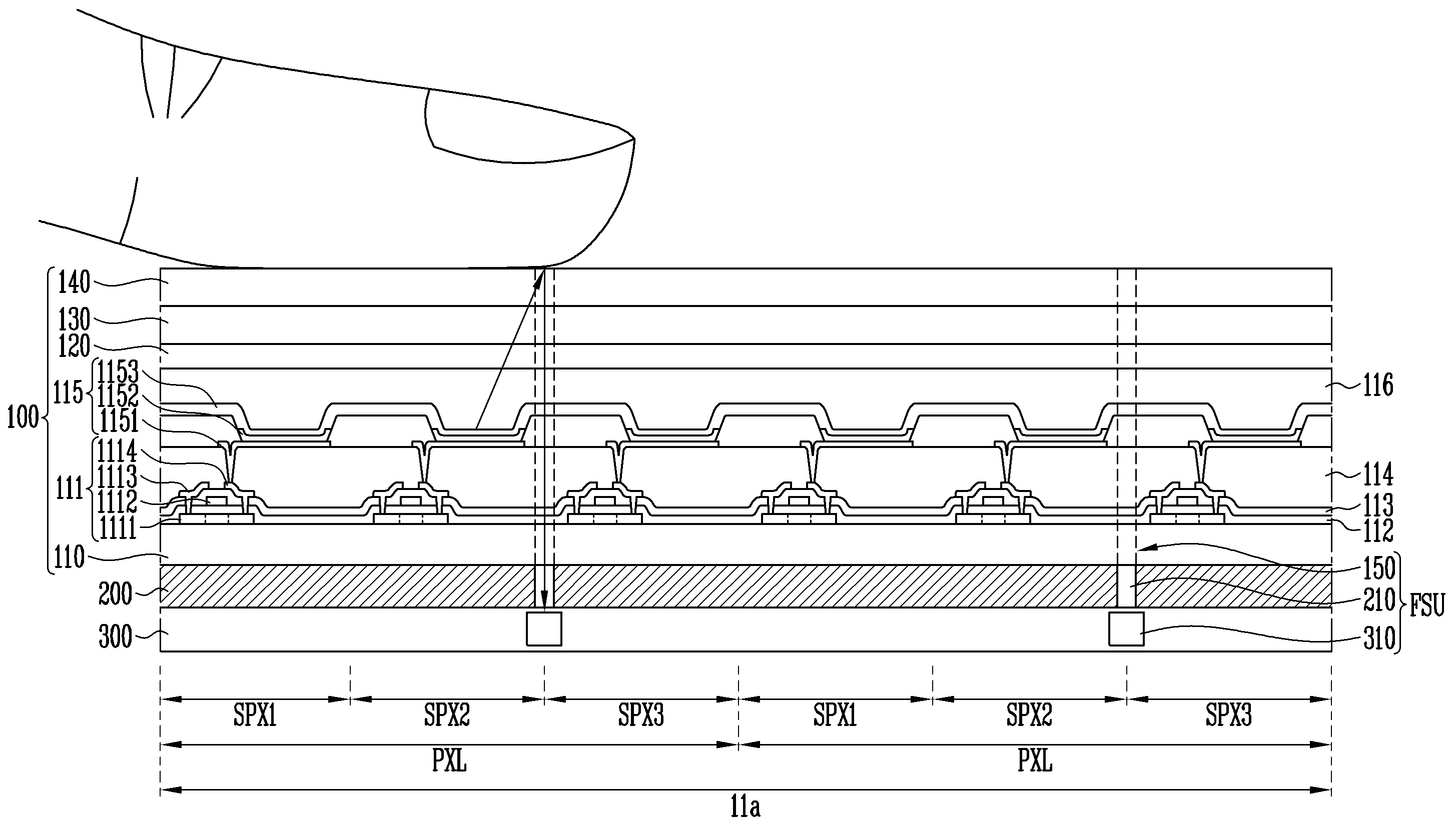
도 13은 본 발명의 일 실시예에 의한 표시장치의 지문 센서 영역을 나타내는 단면도이다. 편의상, 도 13에서는 지문 센서 영역 중 일 영역만을 도시하기로 하며, 각각의 서브 화소들이 형성되는 영역 내에 상기 서브 화소들을 구성하는 일부 구성요소만을 선택적으로 도시하기로 한다. 한편, 도 13에서는 각 서브 화소들 및 지문 센서 유닛을 명확히 도시하기 위하여 손가락의 크기 대비 화소들의 크기를 과장하여 도시하였으나, 실제로 개별 화소들 및 지문 센서 유닛들의 크기와 이들 사이의 피치는 매우 작게 설계될 수 있다. 즉, 실제로 한 손가락의 지문 하부에는 다수의 화소들 및 지문 센서 유닛들이 배치될 수 있고, 이러한 지문 센서 유닛들로부터의 출력신호를 종합함으로써, 손가락의 지문 형태(지문 패턴)을 인식할 수 있게 된다.FIG. 13 is a cross-sectional view showing a fingerprint sensor area of a display device according to an embodiment of the present invention. For convenience, only one area of the fingerprint sensor area is illustrated in FIG. 13, and only some components constituting the sub-pixels within the area where each sub-pixel is formed are selectively illustrated. Meanwhile, in FIG. 13, the size of the pixels is exaggerated relative to the size of the finger in order to clearly illustrate each sub-pixel and the fingerprint sensor unit, but in reality, the size of the individual pixels and the fingerprint sensor units and the pitch between them can be designed to be very small. That is, in reality, a plurality of pixels and fingerprint sensor units can be arranged under the fingerprint of a finger, and by synthesizing output signals from these fingerprint sensor units, the fingerprint shape (fingerprint pattern) of the finger can be recognized.
도 13을 참조하면, 본 발명의 일 실시예에 의한 표시장치는 지문 센서 영역(11a)에 배치된 복수의 지문 센서 유닛들(FSU)을 포함한다. 각각의 지문 센서 유닛(FSU)은 서로 대응하는 투광 경로(150), 도광로(210) 및 수광소자(310)를 포함한다. 예컨대, 각각의 지문 센서 유닛(FSU)은 복수의 투광 경로들(150), 도광로들(210) 및 수광소자들(310) 중 서로 중첩되도록 배치되는 적어도 하나의 투광 경로(150), 도광로(210) 및 수광소자(310)를 포함할 수 있다. 이러한 지문 센서 유닛(FSU)은 주변 화소(PXL)에 포함된 적어도 하나의 발광소자(115)를 지문 센싱을 위한 광원으로서 이용한다. 따라서, 서로 대응하는 투광 경로(150), 도광로(210) 및 수광소자(310)와 더불어, 이들 주변의 화소(PXL)에 구비된 적어도 하나의 발광소자(115)가 각각의 지문 센서 유닛(FSU)을 구성하는 것으로도 볼 수 있다.Referring to FIG. 13, a display device according to an embodiment of the present invention includes a plurality of fingerprint sensor units (FSU) arranged in a fingerprint sensor area (11a). Each fingerprint sensor unit (FSU) includes a light projection path (150), a light guide path (210), and a light receiving element (310) corresponding to each other. For example, each fingerprint sensor unit (FSU) may include at least one light projection path (150), a light guide path (210), and a light receiving element (310) arranged to overlap each other among the plurality of light projection paths (150), light guide paths (210), and light receiving elements (310). Such a fingerprint sensor unit (FSU) uses at least one light emitting element (115) included in a peripheral pixel (PXL) as a light source for fingerprint sensing. Accordingly, it can be seen that at least one light emitting element (115) provided in each pixel (PXL) around the corresponding light projection path (150), light guide path (210) and light receiving element (310) constitutes each fingerprint sensor unit (FSU).
보다 구체적으로, 본 발명의 일 실시예에 의한 표시장치는, 적어도 제1 기판(110)을 포함하며, 실시예에 따라서는 제2 기판(120)을 추가적으로 포함할 수 있다. 일례로, 표시장치는 제1 및 제2 기판(110, 120)을 포함하며 제2 기판(120) 측의 일면(예컨대, 전면)에서 영상을 표시하는 표시패널(100)과, 표시패널(100)의 이면(영상이 표시되는 일면과 반대되는 면, 예컨대, 배면) 측에 배치되는 광 센서층(300)과, 표시패널(100)과 광 센서층(300)의 사이에 배치되는 도광층(200)을 포함할 수 있다.More specifically, a display device according to one embodiment of the present invention includes at least a first substrate (110), and may additionally include a second substrate (120) depending on the embodiment. For example, the display device may include a display panel (100) that displays an image on one side (e.g., a front side) of the second substrate (120) including the first and second substrates (110, 120), a light sensor layer (300) disposed on the back side (a side opposite to the side on which the image is displayed, e.g., a back side) of the display panel (100), and a light guide layer (200) disposed between the display panel (100) and the light sensor layer (300).
표시패널(100)은 제1 기판(110)과, 상기 제1 기판(110)의 제1면 측에 배치되는 제2 기판(120)을 포함한다. 즉, 제1 기판(110) 및 제2 기판(120)은 서로 대향될 수 있다. 실시예에 따라, 표시패널(100)은 제2 기판(120) 측에 배치되는 편광판(130) 및 윈도우(140) 중 적어도 하나를 더 구비할 수 있다.The display panel (100) includes a first substrate (110) and a second substrate (120) arranged on a first surface side of the first substrate (110). That is, the first substrate (110) and the second substrate (120) may face each other. According to an embodiment, the display panel (100) may further include at least one of a polarizing plate (130) and a window (140) arranged on the second substrate (120) side.
실시예에 따라, 제1 기판(110) 및 제2 기판(120) 중 적어도 하나는 유리 기판 혹은 플라스틱 기판일 수 있으나, 이에 한정되지는 않는다. 예컨대, 제1 기판(110) 및/또는 제2 기판(120)은, 폴리에테르술폰(PES, polyethersulfone), 폴리아크릴레이트(polyacrylate), 폴리에테르이미드(PEI, polyetherimide), 폴리에틸렌 나프탈레이트(PEN, polyethylene naphthalate), 폴리에틸렌 테레프탈레이드(PET, polyethylene terephthalate), 폴리페닐렌 설파이드(PPS, polyphenylene sulfide), 폴리아릴레이트(PAR, polyarylate), 폴리이미드(PI, polyimide), 폴리카보네이트(PC, Polycarbonate), 셀룰로오스 트리 아세테이트(TAC) 및 셀룰로오스아세테이트 프로피오네이트(CAP, cellulose acetate propionate) 중 적어도 하나의 물질을 포함한 가요성 기판(flexible substrate)일 수 있다. 또한, 제1 기판(110) 및/또는 제2 기판(120)은 유리(glass) 및 강화 유리 중 하나의 물질을 포함하는 경성 기판(rigid substrate)일 수도 있다. 또한, 제1 기판(110) 및/또는 제2 기판(120)은 투명한 재질의 기판, 즉, 투광성 기판일 수 있다.According to an embodiment, at least one of the first substrate (110) and the second substrate (120) may be, but is not limited to, a glass substrate or a plastic substrate. For example, the first substrate (110) and/or the second substrate (120) may be a flexible substrate including at least one material from among polyethersulfone (PES), polyacrylate, polyetherimide (PEI), polyethylene naphthalate (PEN), polyethylene terephthalate (PET), polyphenylene sulfide (PPS), polyarylate (PAR), polyimide (PI), polycarbonate (PC), cellulose triacetate (TAC), and cellulose acetate propionate (CAP). Additionally, the first substrate (110) and/or the second substrate (120) may be a rigid substrate including one of glass and tempered glass. Additionally, the first substrate (110) and/or the second substrate (120) may be a substrate made of a transparent material, i.e., a light-transmitting substrate.
또한, 실시예에 따라, 제1 기판(110) 및 제2 기판(120) 중 적어도 하나는, 적어도 한 층의 무기막 및/또는 유기막을 포함하는 절연층으로 구현될 수도 있다. 예컨대, 제2 기판(120)은 적어도 한 층의 무기막 및/또는 유기막을 포함하는 박막 봉지층(Thin Film Encapsulation; TFE)일 수 있다.Additionally, according to an embodiment, at least one of the first substrate (110) and the second substrate (120) may be implemented as an insulating layer including at least one layer of an inorganic film and/or an organic film. For example, the second substrate (120) may be a thin film encapsulation (TFE) layer including at least one layer of an inorganic film and/or an organic film.
실시예에 따라, 제1 기판(110)에는 복수의 화소들(PXL)이 구비된다. 예컨대, 제1 기판(110) 및 제2 기판(120)의 사이에는 복수의 화소들(PXL)이 배치될 수 있다. 실시예에 따라, 화소들(PXL) 각각은 복수의 서브 화소들, 일례로, 제1 내지 제3 서브 화소들(SPX1, SPX2, SPX3)을 포함할 수 있다.According to an embodiment, a plurality of pixels (PXL) are provided on the first substrate (110). For example, a plurality of pixels (PXL) may be arranged between the first substrate (110) and the second substrate (120). According to an embodiment, each of the pixels (PXL) may include a plurality of sub-pixels, for example, first to third sub-pixels (SPX1, SPX2, SPX3).
제1 내지 제3 서브 화소들(SPX1, SPX2, SPX3) 각각은, 제1 기판(110)의 제1면 상에 위치되는 트랜지스터(111)와, 상기 트랜지스터(111)에 전기적으로 연결되는 발광소자(115)를 포함할 수 있다. 실시예에 따라, 트랜지스터(111)는, 활성층(1111), 게이트 전극(1112), 소스 및 드레인 전극(1113, 1114)을 포함할 수 있다. 실시예에 따라, 활성층(1111)은 제1 기판(110) 상에 배치되고, 게이트 전극(1112)은 제1 절연막(112)을 사이에 개재하고 활성층(1111)과 중첩되도록 배치될 수 있다. 실시예에 따라, 소스 및 드레인 전극(1113, 1114)은 게이트 전극(1112) 상에 위치된 제2 절연막(113) 상에 배치되어, 제1 및 제2 절연막(112, 113)에 형성된 컨택홀을 통해 활성층(1111)과 연결될 수 있다.Each of the first to third sub-pixels (SPX1, SPX2, SPX3) may include a transistor (111) positioned on a first surface of a first substrate (110) and a light-emitting element (115) electrically connected to the transistor (111). According to an embodiment, the transistor (111) may include an active layer (1111), a gate electrode (1112), and source and drain electrodes (1113, 1114). According to an embodiment, the active layer (1111) may be disposed on the first substrate (110), and the gate electrode (1112) may be disposed to overlap the active layer (1111) with a first insulating film (112) interposed therebetween. According to an embodiment, the source and drain electrodes (1113, 1114) may be disposed on a second insulating film (113) positioned on the gate electrode (1112) and connected to the active layer (1111) through contact holes formed in the first and second insulating films (112, 113).
실시예에 따라, 소스 및 드레인 전극(1113, 1114) 상에는 제3 절연막(114)이 배치되고, 제3 절연막(114) 상에는 발광소자(115)가 배치될 수 있다. 발광소자(115)는 제3 절연막(114)에 형성된 비아홀을 통해 트랜지스터(111)에 전기적으로 연결될 수 있다.According to an embodiment, a third insulating film (114) may be disposed on the source and drain electrodes (1113, 1114), and a light-emitting element (115) may be disposed on the third insulating film (114). The light-emitting element (115) may be electrically connected to the transistor (111) through a via hole formed in the third insulating film (114).
발광소자(115)는 적어도 일 영역에서 서로 중첩되는 제1 전극(1151) 및 제2 전극(1153)과, 상기 제1 및 제2 전극(1151, 1153)의 사이에 개재된 발광층(1152)을 포함한다. 실시예에 따라, 제1 전극(1151) 및 제2 전극(1153)은 각각 애노드 전극 및 캐소드 전극일 수 있으나, 이에 한정되지는 않는다. 예컨대, 화소 구조에 따라서는 트랜지스터(111)에 전기적으로 연결되는 제1 전극(1151)이 캐소드 전극일 수도 있다. 실시예에 따라, 발광소자(115)와 제2 기판(120)의 사이에는 제3 절연막(116)이 배치될 수 있다. The light-emitting element (115) includes a first electrode (1151) and a second electrode (1153) that overlap each other in at least one area, and a light-emitting layer (1152) interposed between the first and second electrodes (1151, 1153). According to an embodiment, the first electrode (1151) and the second electrode (1153) may be an anode electrode and a cathode electrode, respectively, but are not limited thereto. For example, depending on the pixel structure, the first electrode (1151) electrically connected to the transistor (111) may be a cathode electrode. According to an embodiment, a third insulating film (116) may be disposed between the light-emitting element (115) and the second substrate (120).
실시예에 따라, 표시패널(100)은 화소들(PXL) 중 적어도 일부의 화소들(PXL)에 포함된 발광소자들(115)의 주변에 배치되는 복수의 투광 경로들(150)을 포함할 수 있다. 일례로, 표시패널(100)은 각각의 화소들(PXL)과 중첩되도록 배치되며, 상기 화소들(PXL)을 구성하는 일부 서브 화소들, 예컨대 제2 및 제3 서브 화소들(SPX2, SPX3) 사이의 간극에 위치되는 복수의 투광 경로들(150)을 포함할 수 있다.According to an embodiment, the display panel (100) may include a plurality of light-emitting paths (150) arranged around light-emitting elements (115) included in at least some of the pixels (PXL). For example, the display panel (100) may include a plurality of light-emitting paths (150) arranged to overlap each of the pixels (PXL) and positioned in gaps between some of the sub-pixels constituting the pixels (PXL), for example, the second and third sub-pixels (SPX2, SPX3).
실시예에 따라, 투광 경로들(150)은 주변에 배치되는 발광소자들(115)의 발광영역(예컨대, 발광층(1152)이 배치되는 영역)과 어긋나도록 배치될 수 있다. 일례로, 투광 경로들(150)은, 발광소자들(115)로부터 사용자의 지문을 향해 사선 방향으로 방출되어 사용자의 지문에서 수직 방향으로 반사된 광을 수광할 수 있는 위치에 배치될 수 있다. 이와 같이 사용자의 지문에 사선 방향으로 조사된 광을 이용하여 지문을 센싱하게 되면, 지문의 명암이 보다 뚜렷해져서 보다 용이하게 지문 패턴을 파악할 수 있게 된다.According to an embodiment, the light-transmitting paths (150) may be arranged so as to be misaligned with the light-emitting areas of the light-emitting elements (115) arranged around them (e.g., areas where the light-emitting layer (1152) is arranged). For example, the light-transmitting paths (150) may be arranged at positions capable of receiving light emitted diagonally from the light-emitting elements (115) toward the user's fingerprint and reflected vertically from the user's fingerprint. When the fingerprint is sensed using light irradiated diagonally to the user's fingerprint in this way, the brightness of the fingerprint becomes more distinct, so that the fingerprint pattern can be identified more easily.
실시예에 따라, 화소들(PXL)이 제2 기판(120) 방향으로 광을 방출할 때, 투광 경로들(150)은 적어도 하나의 주변 화소(PXL)로부터 방출된 광 중 사용자의 지문에서 반사되어 제1 기판(110) 방향으로 입사되는 반사광의 적어도 일부를 선택적으로 투과시키는 방향으로 연장될 수 있다. 예컨대, 투광 경로들(150)은 표시패널(100)에 직교하는 방향으로 반사된 수직 방향의 반사광을 투과시킬 수 있도록, 표시패널(100)이 배치되는 평면과 직교하는 수직 방향으로 연장될 수 있다. 즉, 실시예에 따라, 투광 경로들(150)의 길이 방향은 표시패널(100)이 배치되는 평면과 교차할 수 있으며, 일례로 직교할 수 있다.According to an embodiment, when the pixels (PXL) emit light toward the second substrate (120), the light transmission paths (150) may extend in a direction to selectively transmit at least a portion of the reflected light that is reflected from a user's fingerprint among the light emitted from at least one surrounding pixel (PXL) and is incident toward the first substrate (110). For example, the light transmission paths (150) may extend in a vertical direction orthogonal to a plane on which the display panel (100) is arranged so as to transmit vertical reflected light reflected in a direction orthogonal to the display panel (100). That is, according to an embodiment, the longitudinal direction of the light transmission paths (150) may intersect the plane on which the display panel (100) is arranged, or may be orthogonal to the plane, for example.
실시예에 따라, 투광 경로들(150)은 사용자의 지문에서 반사되는 반사광 중 미리 설정된 방향의 광만을 선택적으로 투과시키도록 형성될 수 있다. 일례로, 표시패널(100)에 물리적으로 수직 홀(hole)을 뚫거나, 혹은, 투광 경로들(150)에 상응하는 소정의 위치에 광의 투과를 차단하는 물질이 배치되지 않도록 배선 등을 배치할 수 있다.According to an embodiment, the light transmission paths (150) may be formed to selectively transmit only light in a preset direction among the reflected light reflected from the user's fingerprint. For example, a vertical hole may be physically drilled in the display panel (100), or wiring, etc. may be arranged so that a material that blocks the transmission of light is not arranged at a predetermined location corresponding to the light transmission paths (150).
또는, 실시예에 따라, 도 5에서 설명한 바와 같이 활성영역(11)의 내부에 존재하는 투광성 간극을 투광 경로(150)로 이용하고, 이러한 투광 경로(150)와 중첩되도록 투광 경로(150)의 하부에 도광로(210) 및 수광소자(310)를 배치할 수도 있다. 즉, 투광 경로들(150)은 물리적으로 뚫린 홀은 물론, 제1 및 제2 기판(110, 120)이나 발광소자(115)의 제2 전극(1153)과 같이 투명한 물질들로만 구성되어 표시패널(100)과 교차하는 방향으로 광이 투과될 수 있는 경로가 존재하는 영역을 포괄적으로 의미할 수 있다. 즉, 투광 경로(150)는 광이 투과될 수 있도록 표시패널(100)에 형성되는 광학적 개념의 홀을 포괄적으로 의미하는 것으로서, 화소들(PXL)이 배치되는 활성영역(11) 내에 구비되는 차광성 배선들 및/또는 회로소자들 사이의 투광성 간극에 위치될 수 있다.Alternatively, according to an embodiment, a light-transmitting gap existing inside the active region (11) as described in FIG. 5 may be used as a light-transmitting path (150), and the light guide path (210) and the light-receiving element (310) may be arranged below the light-transmitting path (150) so as to overlap with the light-transmitting path (150). That is, the light-transmitting paths (150) may comprehensively mean areas in which a path exists through which light can be transmitted in a direction intersecting with the display panel (100), and which are made only of transparent materials, such as a physically drilled hole, the first and second substrates (110, 120), or the second electrode (1153) of the light-emitting element (115). That is, the light transmission path (150) comprehensively refers to an optical hole formed in the display panel (100) to allow light to pass through, and may be positioned in a light-transmitting gap between light-shielding wires and/or circuit elements provided within the active area (11) where pixels (PXL) are arranged.
실시예에 따라, 표시패널(100)의 이면, 즉 제1 기판(110)의 제2면 측에는 도광층(200) 및 광 센서층(300)이 배치된다. 도광층(200) 및 광 센서층(300)은 표시패널(100)의 투광 경로들(150)에 대응하는 도광로들(210) 및 수광소자들(310)을 포함한다. 일례로, 도광로들(210) 및 수광소자들(310)은 투광 경로들(150)의 하부에 배치될 수 있다.According to an embodiment, a light guide layer (200) and a light sensor layer (300) are arranged on the back surface of the display panel (100), that is, on the second surface side of the first substrate (110). The light guide layer (200) and the light sensor layer (300) include light guide paths (210) and light receiving elements (310) corresponding to the light transmission paths (150) of the display panel (100). For example, the light guide paths (210) and the light receiving elements (310) may be arranged below the light transmission paths (150).
실시예에 따라, 화소들(PXL)이 제2 기판(120) 방향으로 광을 방출한다고 할 때, 도광로들(210)은, 사용자의 지문에서 반사되어 제1 기판(110) 방향으로 재입사되는 반사광 중 투광 경로들(150)을 투과한 광이 투과될 수 있는 방향으로 연장될 수 있다. 예컨대, 도광로들(210)은 투광 경로들(150)의 연장방향과 동일한 방향, 예컨대, 표시패널(100)에 직교하는 수직 방향으로 연장될 수 있다. 즉, 도광로들(210)의 길이 방향은 표시패널(100)이 배치되는 평면과 직교할 수 있다. 이러한 도광로들(210)은 사용자의 지문에서 반사된 반사광 중 소정의 방향에 부합되는 일부의 반사광만을 선별적으로 투과시키는 필터로 기능할 수 있다. 이와 같은 도광로들(210)을 이용할 경우, 별도의 렌즈를 이용하지 않고도 지문 센서 유닛(FSU)을 구성할 수 있다.According to an embodiment, when the pixels (PXL) emit light toward the second substrate (120), the light guide paths (210) may be extended in a direction in which light that has passed through the light transmission paths (150) among the reflected light reflected from the user's fingerprint and re-incident toward the first substrate (110) can be transmitted. For example, the light guide paths (210) may be extended in the same direction as the extension direction of the light transmission paths (150), for example, in a vertical direction orthogonal to the display panel (100). That is, the longitudinal direction of the light guide paths (210) may be orthogonal to a plane on which the display panel (100) is arranged. These light guide paths (210) may function as a filter that selectively transmits only a portion of the reflected light that matches a predetermined direction among the reflected light reflected from the user's fingerprint. When such light guide paths (210) are used, a fingerprint sensor unit (FSU) can be configured without using a separate lens.
실시예에 따라, 도광로들(210)의 모양 및 크기(예컨대, 직경, 단면적 및/또는 높이) 등은 다양하게 변경될 수 있다. 예컨대, 각각의 지문 센서 유닛(FSU)에서 요구되는 수광량 및 해상도 등의 다양한 요인을 고려하여 도광층(200) 내에 다양한 형태의 도광로들(210)을 구성할 수 있을 것이다.Depending on the embodiment, the shape and size (e.g., diameter, cross-sectional area, and/or height) of the light guide paths (210) may be varied. For example, light guide paths (210) of various shapes may be configured within the light guide layer (200) by considering various factors such as the amount of light received and the resolution required by each fingerprint sensor unit (FSU).
실시예에 따라, 수광소자들(310)은 포토 다이오드, CMOS 이미지 센서 및 CCD 카메라 중 하나일 수 있으나, 이에 한정되지는 않는다. 이러한 수광소자들(310)은 투광 경로들(150) 및 도광로들(210)을 통해 입사된 반사광에 상응하는 출력신호를 생성한다. 수광소자들(310)에서 발생된 출력신호는 도시되지 않은 구동회로로 입력되어 사용자의 지문 정보를 생성하는 데에 이용될 수 있다. 즉, 본 발명의 실시예에 의한 표시장치는 수광소자들(310)로부터의 출력신호를 이용하여 표시패널(100) 상에 위치된 손가락의 지문 패턴을 센싱할 수 있다.According to an embodiment, the photodetectors (310) may be, but are not limited to, one of a photodiode, a CMOS image sensor, and a CCD camera. These photodetectors (310) generate output signals corresponding to reflected light incident through the light-transmitting paths (150) and the light-guiding paths (210). The output signals generated from the photodetectors (310) may be input to a driving circuit (not shown) and used to generate fingerprint information of a user. That is, the display device according to an embodiment of the present invention may sense a fingerprint pattern of a finger located on a display panel (100) by using the output signals from the photodetectors (310).
전술한 본 발명의 실시예에 의하면, 화소들(PXL)로부터 방출되는 광을 이용하여 사용자의 지문을 센싱함으로써, 별도의 외부 광원 없이 표시장치의 지문 센서를 구현할 수 있다. 또한, 도광층(200)에 형성된 도광로(210)를 이용하여 반사광을 선택적으로 투과시킴으로써, 지문 패턴에 상응하는 상을 맺기 위한 별도의 렌즈 없이도 지문 센서를 구현할 수 있다. 이에 따라, 지문 센싱 기능을 제공하는 표시장치의 두께를 감소시키고, 제조 비용을 절감할 수 있다.According to the above-described embodiment of the present invention, by sensing a user's fingerprint using light emitted from pixels (PXL), a fingerprint sensor of a display device can be implemented without a separate external light source. In addition, by selectively transmitting reflected light using a light guide path (210) formed in a light guide layer (200), a fingerprint sensor can be implemented without a separate lens for forming an image corresponding to a fingerprint pattern. Accordingly, the thickness of a display device providing a fingerprint sensing function can be reduced, and the manufacturing cost can be reduced.
또한, 본 발명의 실시예에 의하면, 사용자의 지문에서 반사되는 광을 감지하기 위한 광 센서층(300)을 도광층(200)과 함께 표시패널(100)의 이면에 배치한다. 이에 따라, 광 센서층(300)이 사용자에게 시인되는 것을 방지함으로써, 표시장치의 화질 저하를 방지할 수 있다.In addition, according to an embodiment of the present invention, a light sensor layer (300) for detecting light reflected from a user's fingerprint is placed on the back surface of the display panel (100) together with the light guide layer (200). Accordingly, the light sensor layer (300) is prevented from being recognized by the user, thereby preventing deterioration of the image quality of the display device.
도 14는 도 13에 도시된 도광층의 일례를 나타내는 사시도이다.Fig. 14 is a perspective view showing an example of the light guide layer illustrated in Fig. 13.
도 14를 참조하면, 실시예에 따라, 도광층(200)은 도광로들(210)에 상응하는 복수의 개구부들을 포함하는 차광층(201)일 수 있다. 즉, 도광로들(210)은 차광층(201)에 형성된 개구부들(openings 또는 holes)로 구성될 수 있다. 실시예에 따라, 차광층(201)은 블랙 매트릭스일 수 있으나 이에 한정되지는 않으며, 차광성을 보유한 물질로 구성될 수 있다. 이와 같이, 복수의 개구부들을 포함하는 차광층(201)을 이용하여 도광층(200)을 구성하게 되면, 별도의 렌즈 없이 지문 센서 유닛(FSU)을 구현할 수 있게 됨은 물론, 광의 회절에 의한 해상도 저하를 방지할 수 있다.Referring to FIG. 14, according to an embodiment, the light guide layer (200) may be a light shielding layer (201) including a plurality of openings corresponding to light guide paths (210). That is, the light guide paths (210) may be formed by openings (or holes) formed in the light shielding layer (201). According to an embodiment, the light shielding layer (201) may be a black matrix, but is not limited thereto, and may be formed of a material having light shielding properties. In this way, when the light guide layer (200) is formed using the light shielding layer (201) including a plurality of openings, it is possible to implement a fingerprint sensor unit (FSU) without a separate lens, and also prevent resolution degradation due to diffraction of light.
실시예에 따라, 도 14에서는 도광로들(210)을 원기둥 형태로 도시하였으나, 본 발명이 이에 한정되지는 않는다. 예컨대, 도광로들(210)의 형상, 크기 및/또는 그 배치 구조 등은 다양하게 변경 실시될 수 있다.According to an embodiment, the light guide paths (210) are illustrated in a cylindrical shape in FIG. 14, but the present invention is not limited thereto. For example, the shape, size, and/or arrangement structure of the light guide paths (210) may be variously changed.
도 15는 도 13에 도시된 도광층의 다른 예를 나타내는 사시도이다. 도 15에서, 도 14와 유사 또는 동일한 구성요소에 대해서는 동일 부호를 부여하고, 이에 대한 상세한 설명은 생략하기로 한다.Fig. 15 is a perspective view showing another example of the light-guiding layer illustrated in Fig. 13. In Fig. 15, components similar or identical to those in Fig. 14 are given the same reference numerals, and detailed descriptions thereof are omitted.
도 15를 참조하면, 실시예에 따라, 도광층(200)은 도광로들(210)을 구성하는 개구부들에 채워진 컬러 필터(212)를 더 포함할 수 있다. 일례로, 지문 센서 영역(11a)에 배치된 화소들(PXL)이 청색 광을 발광하도록 구동하여 상기 청색 광을 지문 센싱에 이용한다고 할 때, 컬러 필터(212)는 청색 광을 선택적으로 투과시키는 청색 컬러 필터일 수 있다. 이와 같이 도광로들(210) 내에 특정 컬러 필터(212)를 구비하게 되면, 지문에서 반사되는 광에 대한 선별력을 향상시켜 지문 센싱의 신뢰성을 향상시킬 수 있다.Referring to FIG. 15, according to an embodiment, the light guide layer (200) may further include a color filter (212) filled in the openings forming the light guide paths (210). For example, when pixels (PXL) arranged in the fingerprint sensor area (11a) are driven to emit blue light and the blue light is used for fingerprint sensing, the color filter (212) may be a blue color filter that selectively transmits the blue light. In this way, when a specific color filter (212) is provided in the light guide paths (210), the selectivity for light reflected from a fingerprint can be improved, thereby improving the reliability of fingerprint sensing.
도 16은 도 13에 도시된 도광층의 또 다른 예를 나타내는 사시도이다.Fig. 16 is a perspective view showing another example of the light-guiding layer illustrated in Fig. 13.
도 16을 참조하면, 실시예에 따라, 도광층(200')은 도광로들(210')을 구성하는 광섬유(광섬유 다발)를 포함할 수 있다. 즉, 각각의 도광로들(210')은, 상대적으로 높은 굴절률을 가지는 코어(210a')와, 상기 코어(210a')를 감싸며 코어(210a')보다 낮은 굴절률을 가지는 클래딩(210b')을 포함하는 개개의 광섬유로 이루어질 수 있다. 일례로, 광섬유 다발을 잘라서 투광 경로들(150)에 대응하도록 표시패널(100)의 이면에 배치함으로써 도광층(200')을 구성할 수 있다. 또한, 실시예에 따라, 도광로들(210')은 광섬유 외에도 굴절률 차이를 이용한 다른 광 도파로로 구현될 수도 있다.Referring to FIG. 16, according to an embodiment, the light guide layer (200') may include optical fibers (optical fiber bundles) constituting light guide paths (210'). That is, each of the light guide paths (210') may be formed of individual optical fibers including a core (210a') having a relatively high refractive index and a cladding (210b') that surrounds the core (210a') and has a lower refractive index than the core (210a'). For example, the light guide layer (200') may be formed by cutting the optical fiber bundle and arranging it on the back surface of the display panel (100) so as to correspond to the light transmission paths (150). In addition, according to an embodiment, the light guide paths (210') may be implemented as other optical waveguides utilizing a difference in refractive index in addition to optical fibers.
실시예에 따라, 도광층(200')은 도광로들(210')을 구성하는 광섬유보다 낮은 굴절률을 가지며 개별 광섬유 사이의 간극을 메우는 투명 절연층(201')을 더 포함할 수 있다. 투명 절연층(201')을 이용하면, 각각의 광섬유를 투광 경로들(150) 및 수광소자들(310)에 상응하는 위치에 안정적으로 배치할 수 있다.According to an embodiment, the light guide layer (200') may further include a transparent insulating layer (201') that has a lower refractive index than the optical fibers forming the light guide paths (210') and fills the gaps between the individual optical fibers. By using the transparent insulating layer (201'), each optical fiber can be stably placed at a position corresponding to the light transmission paths (150) and the light receiving elements (310).
실시예에 따라, 도광층(200')은 각각의 도광로(210')를 구성하는 광섬유의 코어층(210a')에 포함된 컬러 필터(미도시)를 더 포함할 수 있다. 예컨대, 코어층(210a')의 내부에는 청색 컬러 필터 물질이 포함될 수 있다. 이 경우, 지문에서 반사되는 광에 대한 선별력을 향상시킬 수 있다.According to an embodiment, the light guide layer (200') may further include a color filter (not shown) included in the core layer (210a') of the optical fiber constituting each light guide path (210'). For example, a blue color filter material may be included inside the core layer (210a'). In this case, the selectivity for light reflected from a fingerprint may be improved.
전술한 바와 같은 실시예에 의하면, 광섬유나, 혹은 굴절률 차이를 이용한 광도파로를 이용하여 도광로들(210')을 구성한다. 이에 의해, 투광 경로들(150)을 투과한 특정 방향의 광, 예컨대 수직 방향의 광만이 선별적으로 수광소자들(310)로 입사되도록 할 수 있다.According to the embodiment described above, optical paths (210') are formed using optical fibers or optical waveguides utilizing refractive index differences. As a result, only light in a specific direction, for example, light in a vertical direction, transmitted through the light transmission paths (150) can be selectively incident on the light receiving elements (310).
도 17은 본 발명의 일 실시예에 의한 표시장치의 지문 센싱 원리를 나타내는 도면이다. 편의상, 도 17에서는 수광소자의 일례로서 포토 다이오드를 도시하였으나, 본 발명이 이에 한정되지는 않는다.Fig. 17 is a drawing showing the fingerprint sensing principle of a display device according to one embodiment of the present invention. For convenience, Fig. 17 illustrates a photodiode as an example of a light-receiving element, but the present invention is not limited thereto.
도 17을 참조하면, 본 발명의 일 실시예에 의한 표시장치가 지문 센싱 모드로 구동될 때, 표시패널(100)의 지문 센서 영역(11a)에 포함된 화소들(PXL)의 발광소자들(EL) 중 적어도 일부가 점등된다. 점등된 발광소자(EL)에서 방출된 광 중 적어도 일부는 사용자의 손가락에 부딪쳐 반사된다. 특히, 지문에서 반사된 광 중 표시패널(100)에 형성된 투광 경로들(150)을 투과하도록 수직 방향으로 반사된 광은 해당 영역의 투광 경로(150) 및 도광로(200)를 경유하여 수광소자(310)(예컨대, 포토 다이오드)로 입사된다. 즉, 지문에서 반사된 광 중 적어도 한 쌍의 투광 경로(150) 및 도광로(200)를 통과한 광만이 선별적으로 수광소자(310)로 입사된다.Referring to FIG. 17, when a display device according to one embodiment of the present invention is driven in a fingerprint sensing mode, at least some of the light emitting elements (EL) of the pixels (PXL) included in the fingerprint sensor area (11a) of the display panel (100) are turned on. At least some of the light emitted from the turned on light emitting elements (EL) strikes the user's finger and is reflected. In particular, among the light reflected from the fingerprint, the light reflected in the vertical direction so as to pass through the light transmission paths (150) formed on the display panel (100) passes through the light transmission path (150) and the light guide path (200) of the corresponding area and is incident on the light receiving element (310) (e.g., a photodiode). That is, among the light reflected from the fingerprint, only the light that has passed through at least one pair of light transmission paths (150) and the light guide path (200) is selectively incident on the light receiving element (310).
반사광을 공급받은 수광소자(310)는 이에 대응하는 출력신호를 생성한다. 광 센서층(300)에 배치된 수광소자들(310) 각각의 출력신호는 도시되지 않은 구동회로로 입력된다. 그러면, 구동회로는 수광소자들(310)의 출력신호를 종합적으로 이용하여 사용자의 지문 정보를 생성할 수 있다. 예컨대, 수광소자들(310)로부터의 출력신호를 종합하면, 지문의 굴곡(ridge 및 valley)을 파악할 수 있게 되고, 이에 따라 지문의 형태를 센싱할 수 있게 된다. 이에 의해, 표시장치는 지문 센싱 기능을 제공할 수 있다.The light-receiving element (310) supplied with the reflected light generates an output signal corresponding thereto. The output signal of each of the light-receiving elements (310) arranged in the light sensor layer (300) is input to a driving circuit (not shown). Then, the driving circuit can generate fingerprint information of the user by comprehensively utilizing the output signals of the light-receiving elements (310). For example, by synthesizing the output signals from the light-receiving elements (310), it is possible to identify the curves (ridges and valleys) of the fingerprint, and thus sense the shape of the fingerprint. Accordingly, the display device can provide a fingerprint sensing function.
한편, 투광 경로들(150)은 발광소자들(EL)의 발광영역과 중첩되지 않도록 배치될 수 있다. 즉, 투광 경로들(150)은, 발광소자들(EL)로부터 사용자의 지문을 향해 사선 방향으로 방출되어 사용자의 지문에서 수직 방향으로 반사된 광을 수광할 수 있는 위치에 배치될 수 있다. 또한, 실시예에 따라, 사용자의 지문에 사선 방향으로 광을 조사하기 위하여, 지문 센서 영역(11a)에 배치된 화소들(PXL) 중 일부만을 선별적으로 점등하거나, 지문 센서 영역(11a)의 화소들(PXL)을 복수의 그룹으로 분류하고 각 그룹에 포함된 화소들(PXL)을 순차적으로 점등할 수 있다. 이와 같이 사용자의 지문에 사선 방향으로 광을 조사하게 되면, 이에 따른 음영을 이용하여 지문의 명암을 보다 뚜렷하게 인식할 수 있다. 이에 따라, 지문 센싱의 신뢰성을 향상시킬 수 있다.Meanwhile, the light projection paths (150) may be arranged so as not to overlap with the light-emitting areas of the light-emitting elements (EL). That is, the light projection paths (150) may be arranged at positions capable of receiving light emitted diagonally from the light-emitting elements (EL) toward the user's fingerprint and reflected vertically from the user's fingerprint. In addition, according to an embodiment, in order to irradiate light in a diagonal direction to the user's fingerprint, only some of the pixels (PXL) arranged in the fingerprint sensor area (11a) may be selectively turned on, or the pixels (PXL) of the fingerprint sensor area (11a) may be classified into a plurality of groups and the pixels (PXL) included in each group may be sequentially turned on. In this way, when light is irradiated in a diagonal direction to the user's fingerprint, the brightness of the fingerprint can be recognized more clearly by utilizing the resulting shading. Accordingly, the reliability of fingerprint sensing can be improved.
도 18은 본 발명의 일 실시예에 의한 표시장치의 지문 센서 영역을 나타내는 단면도이다. 도 18에서, 도 13과 유사 또는 동일한 구성요소에 대해서는 동일 부호를 부여하고, 이에 대한 상세한 설명은 생략하기로 한다.Fig. 18 is a cross-sectional view showing a fingerprint sensor area of a display device according to one embodiment of the present invention. In Fig. 18, components similar or identical to those in Fig. 13 are given the same reference numerals, and a detailed description thereof will be omitted.
도 18을 참조하면, 본 발명의 일 실시예에 의한 표시장치는 표시패널(100)과 도광층(200)의 사이에 배치되는 필터층(400)을 더 포함할 수 있다. 실시예에 따라, 필터층(400)은 서브 화소들(SPX1, SPX2, SPX3) 중 일부의 서브 화소들로부터 방출되는 광만을 선택적으로 투과시키는 컬러 필터일 수 있다. 일례로, 소정의 지문 센싱 기간 동안 서브 화소들(SPX1, SPX2, SPX3) 중 청색의 광을 방출하는 서브 화소들을 점등하여 지문 센싱에 이용하는 경우, 필터층(400)은 청색의 광만을 선택적으로 투과시키는 청색 컬러 필터로 구현될 수 있다. 표시패널(100)과 도광층(200)의 사이에 필터층(400)을 배치하게 되면, 지문에서 반사되어 표시패널(100)로 재입사되는 반사광에 대한 선별력을 높일 수 있다.Referring to FIG. 18, a display device according to an embodiment of the present invention may further include a filter layer (400) disposed between the display panel (100) and the light guide layer (200). According to an embodiment, the filter layer (400) may be a color filter that selectively transmits only light emitted from some of the sub-pixels (SPX1, SPX2, SPX3). For example, when the sub-pixels emitting blue light among the sub-pixels (SPX1, SPX2, SPX3) are turned on for fingerprint sensing during a predetermined fingerprint sensing period, the filter layer (400) may be implemented as a blue color filter that selectively transmits only blue light. When the filter layer (400) is disposed between the display panel (100) and the light guide layer (200), the selectivity for reflected light reflected from a fingerprint and re-incident onto the display panel (100) can be increased.
도 19는 본 발명의 일 실시예에 의한 표시장치의 지문 센서 영역을 나타내는 단면도이다. 도 19에서, 도 13과 유사 또는 동일한 구성요소에 대해서는 동일 부호를 부여하고, 이에 대한 상세한 설명은 생략하기로 한다.Fig. 19 is a cross-sectional view showing a fingerprint sensor area of a display device according to one embodiment of the present invention. In Fig. 19, components similar or identical to those in Fig. 13 are given the same reference numerals, and a detailed description thereof will be omitted.
도 19를 참조하면, 본 발명의 일 실시예에 의한 표시장치는 활성영역(11)의 적어도 일 영역에 위치되는 터치 센서층(160)을 더 포함한다. 실시예에 따라, 터치 센서층(160)은 활성영역(11) 중, 지문 센서 유닛들(FSU)이 위치되는 소정의 지문 센서 영역(11a)에 배치된 적어도 하나의 터치 센서 전극(162)을 포함할 수 있다. 일례로, 지문 센서 영역(11a)에는 화소들(PXL) 및 지문 센서 유닛들(FSU)과 중첩되는 복수의 터치 센서 전극들(162)이 배치될 수 있다.Referring to FIG. 19, a display device according to one embodiment of the present invention further includes a touch sensor layer (160) positioned in at least one area of an active area (11). According to an embodiment, the touch sensor layer (160) may include at least one touch sensor electrode (162) positioned in a predetermined fingerprint sensor area (11a) in which fingerprint sensor units (FSU) are positioned among the active area (11). For example, a plurality of touch sensor electrodes (162) overlapping pixels (PXL) and fingerprint sensor units (FSU) may be positioned in the fingerprint sensor area (11a).
실시예에 따라, 터치 센서층(160)은 제2 기판(120)의 일면, 예컨대 상부면 측에 배치될 수 있으나, 본 발명이 이에 한정되지는 않는다. 즉, 터치 센서층(160)의 위치는 다양하게 변경 실시될 수 있다. 예컨대, 터치 센서층(160)은 제2 기판(120)의 내부면(예컨대, 하부면) 및/또는 외부면(예컨대, 상부면)에 배치되어 표시패널(100)과 일체로 구현될 수 있다. 또는, 터치 센서층(160)은 표시패널(100)과 별개로 구성되어 표시패널(100)의 적어도 일면 측에 부착될 수 있다. 또한, 실시예에 따라, 터치 센서층(160)은 경성의 기판 부재 혹은 가요성의 기판 부재 상에 구현된 경성 혹은 가요성의 터치 센서층(160)일 수 있다.According to an embodiment, the touch sensor layer (160) may be disposed on one surface of the second substrate (120), for example, the upper surface, but the present invention is not limited thereto. That is, the position of the touch sensor layer (160) may be variously changed. For example, the touch sensor layer (160) may be disposed on an inner surface (for example, the lower surface) and/or an outer surface (for example, the upper surface) of the second substrate (120) and may be implemented integrally with the display panel (100). Alternatively, the touch sensor layer (160) may be configured separately from the display panel (100) and attached to at least one surface of the display panel (100). In addition, according to an embodiment, the touch sensor layer (160) may be a rigid or flexible touch sensor layer (160) implemented on a rigid substrate member or a flexible substrate member.
실시예에 따라, 이러한 터치 센서층(160)을 지문 센싱에 활용할 수 있다. 일례로, 터치 센서층(160)으로부터의 터치 신호에 대응하여 손가락의 접촉 여부 및/또는 그 영역을 감지하고, 지문 센싱 모드를 활성화시킬 수 있다.According to an embodiment, the touch sensor layer (160) may be utilized for fingerprint sensing. For example, in response to a touch signal from the touch sensor layer (160), whether a finger is in contact and/or its area may be detected, and a fingerprint sensing mode may be activated.
또한, 실시예에 따라, 터치 신호가 발생한 영역을 지문 센서 영역(11a)으로 설정하고, 설정된 영역의 화소들(PXL)을 지문 센싱 모드로 구동할 수도 있다. 예컨대, 활성영역(11)의 전체에 걸쳐 소정의 해상도로 지문 센서 유닛들(FSU)을 배치한 표시장치에 있어서, 터치 신호가 발생한 영역을 포함하는 소정의 영역을 실시간으로 지문 센서 영역(11a)으로 설정할 수 있다.In addition, according to an embodiment, an area where a touch signal is generated may be set as a fingerprint sensor area (11a), and pixels (PXL) of the set area may be driven in a fingerprint sensing mode. For example, in a display device in which fingerprint sensor units (FSU) are arranged at a predetermined resolution over the entire active area (11), a predetermined area including an area where a touch signal is generated may be set as a fingerprint sensor area (11a) in real time.
또한, 실시예에 따라, 터치 신호가 발생한 영역에 배치된 복수의 화소들(PXL)을 동시에 발광시킴으로써, 지문 센서 영역(11a)을 표시할 수 있다. 한편, 활성영역(11) 중 일부 영역만이 지문 센서 영역(11a)이거나, 터치 센서층(160)이 구비되지 않은 표시장치의 경우, 터치 신호가 발생하지 않았더라도 지문 센싱 기간의 초기에 지문 센서 영역(11a)의 화소들(PXL) 중 적어도 일부를 발광시킬 수 있다. 이에 의해, 지문 센서 영역(11a)이 표시되고, 사용자는 지문 센서 영역(11a)을 용이하게 인지할 수 있게 된다. 즉, 실시예에 따라, 미리 설정된 특정 지문 센서 영역(11a), 혹은 터치 센서층(160)에 의해 감지된 지문 센서 영역(11a)의 화소들(PXL)을 발광시켜 지문 센서 영역(11a)을 사용자에게 알릴 수 있다.In addition, according to an embodiment, the fingerprint sensor area (11a) can be displayed by simultaneously emitting light on a plurality of pixels (PXL) arranged in an area where a touch signal has been generated. Meanwhile, in the case of a display device in which only a part of the active area (11) is a fingerprint sensor area (11a) or a touch sensor layer (160) is not provided, at least a part of the pixels (PXL) of the fingerprint sensor area (11a) can be illuminated at the beginning of the fingerprint sensing period even if a touch signal has not been generated. Thereby, the fingerprint sensor area (11a) is displayed, and the user can easily recognize the fingerprint sensor area (11a). That is, according to an embodiment, the fingerprint sensor area (11a) can be notified to the user by emitting light on a specific fingerprint sensor area (11a) that is preset, or the pixels (PXL) of the fingerprint sensor area (11a) detected by the touch sensor layer (160).
전술한 바와 같이, 터치 센서층(160)을 지문 센싱에 활용하게 되면, 표시장치에서 보다 다양한 기능을 제공할 수 있다.As described above, if the touch sensor layer (160) is utilized for fingerprint sensing, the display device can provide more diverse functions.
도 20은 본 발명의 일 실시예에 의한 표시장치의 구동방법을 나타내는 순서도이다. 특히, 도 20은 앞서 설명한 실시예들에서와 같이 화소들을 지문 센싱을 위한 광원으로 이용하며, 표시패널의 일면(예컨대, 영상이 표시되는 면에 대향되는 이면)에 배치된 도광층 및 광 센서층을 포함하는 표시장치의 지문 센싱 기간 동안의 구동방법을 나타내는 순서도이다. 그리고, 도 21은 본 발명의 일 실시예에 의한 지문 센서 영역의 화소들을 구동하는 구동방법 실시예를 나타내는 도면이다. 특히, 도 21은 지문 센싱 기간 동안 지문 센서 영역의 화소들을 구동하는 구동방법의 실시예를 나타내는 도면이다.FIG. 20 is a flowchart showing a method for driving a display device according to an embodiment of the present invention. In particular, FIG. 20 is a flowchart showing a method for driving a display device including a light guide layer and a light sensor layer arranged on one side of a display panel (e.g., a back side opposite to a side on which an image is displayed) while using pixels as a light source for fingerprint sensing, as in the embodiments described above, during a fingerprint sensing period. And FIG. 21 is a diagram showing an embodiment of a driving method for driving pixels in a fingerprint sensor area according to an embodiment of the present invention. In particular, FIG. 21 is a diagram showing an embodiment of a driving method for driving pixels in a fingerprint sensor area during a fingerprint sensing period.
도 20을 참조하면, 본 발명의 실시예에 의한 표시장치의 구동방법은, 지문 센싱 모드를 활성화하는 단계(ST10)와, 지문 센서 영역(11a)의 화소(PXL)를 점등하는 단계(ST20)와, 지문에서 반사되는 반사광을 수광하는 단계(ST30)와, 지문 정보를 생성하는 단계(ST40)를 포함한다.Referring to FIG. 20, a method for driving a display device according to an embodiment of the present invention includes a step of activating a fingerprint sensing mode (ST10), a step of lighting a pixel (PXL) of a fingerprint sensor area (11a) (ST20), a step of receiving reflected light reflected from a fingerprint (ST30), and a step of generating fingerprint information (ST40).
실시예에 따라, 지문 센싱 모드를 활성화하는 단계(ST10)는 제어신호에 대응하여 지문 센싱 모드를 활성화하는 단계일 수 있다 실시예에 따라, 제어신호는 사용자의 선택에 따라 발생하는 제어신호일 수 있다. 또는, 제어신호는 컨텐츠(contents)에 따라, 표시장치를 제어하는 시스템으로부터 공급되는 제어신호일 수도 있다.According to an embodiment, the step of activating the fingerprint sensing mode (ST10) may be a step of activating the fingerprint sensing mode in response to a control signal. According to an embodiment, the control signal may be a control signal generated according to a user's selection. Alternatively, the control signal may be a control signal supplied from a system that controls the display device according to contents.
일례로, 사용자는 도 19에 도시된 터치 센서층(160)을 통해 지문 센싱 모드를 활성화시키기 위한 터치 신호를 입력할 수 있다. 그러면, 사용자에 의한 터치 신호에 대응하여 지문 센싱 모드를 활성화하기 위한 제어신호가 생성될 수 있다.For example, a user may input a touch signal to activate a fingerprint sensing mode through the touch sensor layer (160) illustrated in FIG. 19. Then, a control signal to activate the fingerprint sensing mode may be generated in response to the touch signal by the user.
또한, 실시예에 따라, 터치 신호가 발생한 영역을 지문 센서 영역(11a)으로 설정할 수도 있다. 일례로, 터치 신호가 발생한 지점으로부터 소정 범위의 영역을 지문 센서 영역(11a)으로 실시간으로 설정할 수 있다.In addition, depending on the embodiment, the area where the touch signal is generated may be set as the fingerprint sensor area (11a). For example, an area within a predetermined range from the point where the touch signal is generated may be set as the fingerprint sensor area (11a) in real time.
또한, 실시예에 따라, 터치 신호가 발생한 영역의 화소들(PXL) 중 적어도 일부를 동시에 점등함으로써, 터치 신호에 따라 설정된 지문 센서 영역(11a)을 표시할 수 있다. 이에 따라, 사용자는 지문 센서 영역(11a)을 용이하게 파악하고, 지문 센싱을 위해 해당 영역을 터치할 수 있다.In addition, according to an embodiment, by simultaneously lighting at least some of the pixels (PXL) in an area where a touch signal has occurred, a fingerprint sensor area (11a) set according to a touch signal can be displayed. Accordingly, a user can easily identify the fingerprint sensor area (11a) and touch the area for fingerprint sensing.
한편, 실시예에 따라, 터치 신호의 발생 여부와 무관하게, 지문 센싱 모드가 활성화되는 지문 센싱 기간의 초기에, 소정의 지문 센서 영역(11a)에 배치된 화소들(PXL) 중 적어도 일부를 동시에 점등함으로써, 지문 센서 영역(11a)을 표시할 수도 있다.Meanwhile, according to an embodiment, regardless of whether a touch signal is generated, at the beginning of a fingerprint sensing period in which a fingerprint sensing mode is activated, at least some of the pixels (PXL) arranged in a given fingerprint sensor area (11a) may be simultaneously turned on to display the fingerprint sensor area (11a).
실시예에 따라, 지문 센서 영역(11a)의 화소(PXL)를 점등하는 단계(ST20)는, 상기 지문 센서 영역(11a)에 위치된 화소들(PXL) 중 적어도 일부의 화소들(PXL)을 소정 간격 및/또는 소정 순서로 점등하는 단계일 수 있다.According to an embodiment, the step (ST20) of lighting up pixels (PXL) of the fingerprint sensor area (11a) may be a step of lighting up at least some of the pixels (PXL) located in the fingerprint sensor area (11a) at a predetermined interval and/or in a predetermined order.
일례로, 지문 센서 영역(11a)의 화소(PXL)를 점등하는 단계(ST20)에서는, 도 21에 도시된 실시예와 같이 지문 센서 영역(11a)에 위치된 화소들(PXL)을 복수의 그룹들(GR)로 분류하고, 각각의 그룹(GR) 내에 포함된 화소들(PXL)을 순차적으로 발광시키는 단계일 수 있다.For example, in the step (ST20) of lighting up the pixels (PXL) of the fingerprint sensor area (11a), as in the embodiment illustrated in FIG. 21, the pixels (PXL) located in the fingerprint sensor area (11a) may be classified into a plurality of groups (GR), and the pixels (PXL) included in each group (GR) may be sequentially lit.
또한, 실시예에 따라, 지문 센서 영역(11a)의 화소(PXL)를 점등하는 단계(ST20)에서는, 지문 센싱 모드가 활성화되는 지문 센싱 기간을 복수의 서브 기간들로 분할하고, 각각의 서브 기간 동안 지문 센서 영역(11a)에 위치된 화소들(PXL) 중 소정 간격으로 배치된 일부 화소들(PXL)만을 선택적으로 발광시킬 수 있다.In addition, according to an embodiment, in the step (ST20) of lighting up the pixels (PXL) of the fingerprint sensor area (11a), the fingerprint sensing period in which the fingerprint sensing mode is activated may be divided into a plurality of sub-periods, and during each sub-period, only some pixels (PXL) arranged at a predetermined interval among the pixels (PXL) located in the fingerprint sensor area (11a) may be selectively illuminated.
실시예에 따라, 화소들(PXL)을 지문 센싱 모드로 구동함에 있어서, 도 6 및 도 7의 실시예에서 설명한 주사신호, 발광 제어신호 및/또는 데이터 신호를 제어신호로 이용하여, 화소들(PXL)의 발광을 개별적으로 제어할 수 있다. 예컨대, 지문 센서 영역(11a)의 화소들(PXL)은 지문 센싱 모드에 대응하는 제어신호에 응답하여 선택적으로 발광할 수 있다. 또한, 실시예에 따라, 지문 센서 영역(11a)의 화소들(PXL)은 복수 개씩 나뉘어 복수의 그룹들(GR)을 형성하되, 각 그룹(GR)에 포함된 화소들(PXL)은 지문 센싱 모드에 대응하는 제어신호에 응답하여 순차적으로 발광할 수 있다.According to an embodiment, when driving pixels (PXL) in a fingerprint sensing mode, the scanning signal, the emission control signal and/or the data signal described in the embodiments of FIGS. 6 and 7 may be used as control signals to individually control the emission of pixels (PXL). For example, the pixels (PXL) of the fingerprint sensor area (11a) may selectively emit light in response to a control signal corresponding to the fingerprint sensing mode. In addition, according to an embodiment, the pixels (PXL) of the fingerprint sensor area (11a) may be divided into a plurality of groups (GR), and the pixels (PXL) included in each group (GR) may sequentially emit light in response to a control signal corresponding to the fingerprint sensing mode.
도 21에 도시된 실시예에서와 같이, 지문 센서 영역(11a)에 위치된 화소들(PXL) 중 적어도 일부의 화소들(PXL)을 소정 간격 및/또는 소정 순서로 점등하여 지문 센싱에 이용하게 되면, 점등된 화소들(PXL)의 사이에서 발생할 수 있는 크로스 토크를 최소화할 수 있다. 이에 따라, 지문 센싱의 신뢰성을 향상시킬 수 있다. 도 21에 도시된 바와 같이, 화소(PXL)의 제1 서브 세트가 발광할 때, 제1 서브 세트의 화소(PXL) 사이에 위치하며 제1 서브 세트의 화소(PXL)들을 상호 구분하는, 화소(PXL)의 제2 서브 세트는 비발광할 수 있다.As in the embodiment illustrated in FIG. 21, when at least some of the pixels (PXL) located in the fingerprint sensor area (11a) are turned on at predetermined intervals and/or in a predetermined order and used for fingerprint sensing, crosstalk that may occur between the turned-on pixels (PXL) can be minimized. Accordingly, the reliability of fingerprint sensing can be improved. As illustrated in FIG. 21, when a first subset of pixels (PXL) emits light, a second subset of pixels (PXL), which is located between the pixels (PXL) of the first subset and distinguishes the pixels (PXL) of the first subset from each other, can not emit light.
실시예에 따라, 지문에서 반사되는 반사광을 수광하는 단계(ST30)는, 사용자의 지문에서 반사되는 반사광 중, 도광층(200)을 경유하여 광 센서층(300)으로 입사되는 반사광을 수광하는 단계일 수 있다. 예컨대, 반사광을 수광하는 단계(ST30)는, 지문에서 반사되는 반사광 중 표시패널(100)의 투광 경로들(150) 및 도광층(200)의 도광로들(210)을 통과한 광이 광 센서층(300)의 수광소자들(310)로 입사되는 단계일 수 있다. 이때, 수광소자들(310)은 수광된 반사광에 대응하는 출력신호를 생성한다.According to an embodiment, the step (ST30) of receiving reflected light reflected from a fingerprint may be a step of receiving reflected light that is incident on the light sensor layer (300) via the light guide layer (200), among the reflected light reflected from the user's fingerprint. For example, the step (ST30) of receiving reflected light may be a step of transmitting light reflected from a fingerprint, which has passed through the light transmission paths (150) of the display panel (100) and the light guide paths (210) of the light guide layer (200), to the light receiving elements (310) of the light sensor layer (300). At this time, the light receiving elements (310) generate an output signal corresponding to the received reflected light.
실시예에 따라, 지문 정보를 생성하는 단계(ST40)는, 수광소자들(310)로부터의 출력신호를 이용하여 사용자의 지문 정보를 생성하는 단계일 수 있다. 일례로, 수광소자들(310)로부터의 출력신호를 종합하여 표시패널(100) 상에 위치된 사용자의 지문 패턴을 센싱할 수 있다.According to an embodiment, the step (ST40) of generating fingerprint information may be a step of generating the user's fingerprint information using output signals from the light-receiving elements (310). For example, the output signals from the light-receiving elements (310) may be synthesized to sense the user's fingerprint pattern located on the display panel (100).
또한, 실시예에 따라, 지문 정보를 생성하는 단계(ST40)는, 지문 센서 영역(11a)을 감지하는 단계와, 광 센서층(300)에 포함된 수광소자들(310) 중, 감지된 지문 센서 영역(11a)에 배치된 수광소자들(310)로부터 출력되는 출력신호를 선별하는 단계와, 상기 선별된 출력신호를 종합하여 지문 정보를 생성하는 단계를 포함할 수 있다. 실시예에 따라, 지문 센서 영역(11a)을 감지하는 단계는, 미리 결정된 지문 센서 영역(11a)을 인지 혹은 파악하거나, 혹은 새로 설정하는 단계일 수 있다. 예컨대, 기 저장된 영역 정보를 이용하여 소정의 지문 센서 영역(11a)을 감지하거나, 혹은 터치 신호 등의 발생 여부를 확인하여 상기 터치 신호가 발생한 영역을 지문 센서 영역(11a)으로 설정할 수 있다.In addition, according to an embodiment, the step (ST40) of generating fingerprint information may include a step of detecting a fingerprint sensor area (11a), a step of selecting output signals output from the light receiving elements (310) disposed in the detected fingerprint sensor area (11a) among the light receiving elements (310) included in the optical sensor layer (300), and a step of generating fingerprint information by synthesizing the selected output signals. According to an embodiment, the step of detecting the fingerprint sensor area (11a) may be a step of recognizing or identifying a predetermined fingerprint sensor area (11a), or a step of newly setting it. For example, a predetermined fingerprint sensor area (11a) may be detected using previously stored area information, or an area where a touch signal or the like has been generated may be set as the fingerprint sensor area (11a) by checking whether a touch signal or the like has been generated.
실시예에 따라, 이러한 지문 정보의 생성 단계는, 도시되지 않은 구동 회로 측에 구비된 지문 센서 제어부(혹은 지문 센서 구동부)에서 수행되거나, 혹은 터치 센서 제어부(혹은, 터치 센서 구동부)와 통합된 통합 제어부 등에서 수행될 수 있다.According to an embodiment, the step of generating such fingerprint information may be performed in a fingerprint sensor control unit (or fingerprint sensor driving unit) provided on the driving circuit side that is not shown, or in an integrated control unit integrated with a touch sensor control unit (or touch sensor driving unit).
실시예에 따라, 센싱된 지문 정보는 사용자를 식별하거나, 새로운 사용자를 등록하는 등의 다양한 용도로 활용될 수 있다. 예컨대, 미리 저장된 특정 사용자의 지문 정보와 지문 센서를 통해 센싱된 지문 정보를 비교함으로써, 사용자를 식별할 수 있다.Depending on the embodiment, the sensed fingerprint information may be utilized for various purposes, such as identifying a user or registering a new user. For example, a user may be identified by comparing fingerprint information sensed through a fingerprint sensor with fingerprint information of a specific user stored in advance.
본 발명의 기술 사상은 전술한 실시예에 따라 구체적으로 기술되었으나, 상기 실시예는 그 설명을 위한 것이며 그 제한을 위한 것이 아님을 주의하여야 한다. 또한, 본 발명의 기술 분야의 통상의 지식을 가진 자라면 본 발명의 기술 사상의 범위 내에서 다양한 변형 예가 가능함을 이해할 수 있을 것이다. Although the technical idea of the present invention has been specifically described in accordance with the above-described embodiments, it should be noted that the above-described embodiments are for the purpose of explanation and not for the purpose of limitation. In addition, those skilled in the art will understand that various modifications are possible within the scope of the technical idea of the present invention.
본 발명의 범위는 명세서의 상세한 설명에 기재된 내용으로 한정되는 것이 아니라, 특허 청구범위에 의해 정해져야만 할 것이다. 또한, 특허 청구범위의 의미 및 범위, 그리고 그 균등 개념으로부터 도출되는 모든 변경 또는 변형된 형태가 본 발명의 범위에 포함되는 것으로 해석되어야 할 것이다.The scope of the present invention should not be limited to the contents described in the detailed description of the specification, but should be determined by the scope of the patent claims. In addition, all changes or modifications derived from the meaning and scope of the patent claims and their equivalent concepts should be interpreted as being included in the scope of the present invention.
10, 100: 표시패널 11: 활성영역
11a: 지문 센서 영역 12: 비활성영역
110, 120: 제1, 제2 기판 111: 박막 트랜지스터
115: 발광소자 150: 투광 경로
160: 터치 센서층 162: 터치 센서 전극
200, 200': 도광층 201: 차광층
210: 도광로(개구부) 210': 도광로(광섬유)
300: 광 센서층 310: 수광소자
400: 필터층 FSU: 지문 센서 유닛
PXL: 화소 SPX: 서브 화소10, 100: Display panel 11: Active area
11a: Fingerprint sensor area 12: Inactive area
110, 120: first and second substrates 111: thin film transistor
115: Light emitting element 150: Light transmission path
160: Touch sensor layer 162: Touch sensor electrode
200, 200': Light-guiding layer 201: Light-shielding layer
210: Light source (opening) 210': Light source (optical fiber)
300: Light sensor layer 310: Photodetector
400: Filter layer FSU: Fingerprint sensor unit
PXL: Pixel SPX: Sub Pixel
Claims (31)
상기 제1 기판에 배치되며, 상기 화소들 사이의 투광 경로들에 대응하는 복수의 수광소자들을 포함하는 광 센서층; 및
물질층과 복수의 도광로들을 포함하고, 상기 물질층은 상기 화소들과 상기 광 센서층의 사이에 배치되며 복수의 홀들을 포함하고, 상기 도광로들은 상기 투광 경로들에 각각 대응하며 상기 홀들 각각 내에 위치하는, 도광층;을 포함하고,
상기 물질층은 차광층인 표시장치.A display panel including a first substrate and a plurality of pixels provided on the first substrate and including light-emitting elements;
An optical sensor layer disposed on the first substrate and including a plurality of light-receiving elements corresponding to light transmission paths between the pixels; and
A light guide layer comprising a material layer and a plurality of light paths, the material layer being disposed between the pixels and the light sensor layer and including a plurality of holes, the light guide paths respectively corresponding to the light transmission paths and positioned within each of the holes;
A display device in which the above material layer is a light-blocking layer.
상기 화소들은 상기 제1 기판의 제1면에 구비되고, 상기 광 센서층은 상기 제1 기판의 제2면 측에 배치되는 표시장치.In the first paragraph,
A display device in which the pixels are provided on a first surface of the first substrate, and the light sensor layer is disposed on a second surface of the first substrate.
상기 화소들은 상기 제1 기판의 상부로 광을 방출하며, 상기 투광 경로들 및 상기 도광로들 각각은, 적어도 하나의 화소로부터 방출된 광 중 상기 제1 기판 방향으로 재입사되는 반사광의 적어도 일부를 투과시키는 방향으로 연장된 표시장치.In the first paragraph,
A display device in which the pixels emit light toward an upper portion of the first substrate, and each of the light transmission paths and the light guide paths extends in a direction that transmits at least a portion of reflected light re-incident toward the first substrate among the light emitted from at least one pixel.
상기 투광 경로들 및 상기 도광로들의 길이 방향 및 상기 홀들의 길이 방향은 상기 표시패널이 배치되는 평면과 직교하는 표시장치.In the third paragraph,
A display device in which the longitudinal directions of the above light projection paths and the above light guide paths and the longitudinal directions of the holes are orthogonal to the plane on which the display panel is arranged.
상기 투광 경로들, 상기 도광로들 및 상기 수광소자들 중, 서로 중첩되도록 배치되는 적어도 하나의 투광 경로, 수광소자 및 도광로에 의해 구성되는 지문 센서 유닛을 포함하는 표시장치.In the first paragraph,
A display device including a fingerprint sensor unit configured by at least one light projection path, a light receiving element and a light guide path, among the light projection paths, the light guide paths and the light receiving elements, which are arranged to overlap each other.
상기 지문 센서 유닛은, 소정의 지문 센서 영역 내에 어레이 형태로 다수 배열되는 표시장치.In paragraph 5,
The above fingerprint sensor unit is a display device in which a plurality of fingerprint sensor units are arranged in an array form within a predetermined fingerprint sensor area.
상기 지문 센서 영역은, 상기 화소들이 배치되는 활성영역의 적어도 일 영역에 배치되는 표시장치.In Article 6,
A display device in which the fingerprint sensor area is arranged in at least one area of the active area in which the pixels are arranged.
상기 지문 센서 유닛은, 적어도 일 영역이 적어도 하나의 화소와 중첩되는 표시장치.In paragraph 5,
The fingerprint sensor unit is a display device in which at least one area overlaps with at least one pixel.
상기 지문 센서 유닛은, 서로 인접한 복수의 화소들 사이의 영역에 배치되는 표시장치.In paragraph 5,
The above fingerprint sensor unit is a display device arranged in an area between a plurality of adjacent pixels.
상기 투광 경로들은, 상기 화소들 중 적어도 일부의 화소들에 포함된 발광소자들의 주변에 배치되는 표시장치.In the first paragraph,
A display device in which the above light-emitting paths are arranged around light-emitting elements included in at least some of the pixels.
상기 투광 경로들은, 상기 화소들이 배치되는 활성영역 내에 구비되는 차광성 배선들 및 회로소자들 사이의 간극에 위치되는 표시장치.In Article 10,
A display device in which the above light-transmitting paths are located in the gaps between the light-shielding wires and circuit elements provided within the active area in which the pixels are arranged.
상기 도광로들은 복수의 개구부들을 포함하고,
상기 물질층은 상기 도광로들 사이에 위치하는 차광 부분들을 포함하는 표시장치.In the first paragraph,
The above light paths include a plurality of openings,
A display device in which the material layer includes light-shielding portions positioned between the light paths.
상기 도광층은, 상기 개구부들에 채워진 컬러 필터를 더 포함하는 표시장치.In Article 12,
A display device wherein the light-guiding layer further includes a color filter filled in the openings.
상기 도광층은, 상기 도광로들을 구성하는 광섬유를 포함하는 표시장치. In the first paragraph,
The above light-guiding layer is a display device including optical fibers constituting the light-guiding paths.
상기 물질층은, 상기 광섬유보다 낮은 굴절률을 가지며 상기 광섬유 사이의 간극을 메우는 투명 절연층을 더 포함하는 표시장치.In Article 14,
A display device wherein the material layer further includes a transparent insulating layer having a lower refractive index than the optical fiber and filling a gap between the optical fibers.
상기 광섬유는 코어층에 포함된 컬러 필터 물질을 포함하는 표시장치.In Article 14,
The above optical fiber is a display device including a color filter material included in a core layer.
상기 표시패널과 상기 도광층의 사이에 배치되는 필터층을 더 구비하는 표시장치.In the first paragraph,
A display device further comprising a filter layer disposed between the display panel and the light guide layer.
상기 화소들 각각은 서로 다른 색상의 광을 방출하는 복수의 서브 화소들을 포함하며,
상기 필터층은, 상기 서브 화소들 중 일부의 서브 화소들로부터 방출되는 광만을 선택적으로 투과시키는 컬러 필터인 표시장치.In Article 17,
Each of the above pixels includes multiple sub-pixels that emit light of different colors,
A display device in which the filter layer is a color filter that selectively transmits only light emitted from some of the sub-pixels among the sub-pixels.
상기 수광소자들 각각은, 상기 투광 경로들 및 상기 도광로들을 통해 입사된 광에 대응하는 출력신호를 생성하는 표시장치.In the first paragraph,
A display device in which each of the above photodetectors generates an output signal corresponding to light incident through the light projection paths and the light guide paths.
상기 수광소자들로부터의 출력신호를 이용하여 상기 표시패널 상에 위치된 손가락의 지문 형태를 센싱하는 표시장치. In Article 19,
A display device that senses the fingerprint shape of a finger located on the display panel using output signals from the above photodetectors.
상기 화소들이 배치되는 활성영역의 적어도 일 영역에 위치되는 터치 센서층을 더 포함하는 표시장치.In the first paragraph,
A display device further comprising a touch sensor layer positioned in at least one area of an active area where the pixels are arranged.
상기 터치 센서층은, 상기 투광 경로들, 상기 수광소자들 및 상기 도광로들이 위치되는 소정의 지문 센서 영역에 배치된 적어도 하나의 터치 센서 전극을 포함하는 표시장치.In Article 21,
A display device including at least one touch sensor electrode arranged in a predetermined fingerprint sensor area where the light-transmitting paths, the light-receiving elements, and the light-guiding paths are located.
상기 광 센서층이 배치되는 지문 센서 영역의 화소들은, 지문 센싱 모드에 대응하는 제어신호에 응답하여 선택적으로 발광하는 표시장치.In the first paragraph,
A display device in which pixels in a fingerprint sensor area where the above-mentioned light sensor layer is arranged selectively emit light in response to a control signal corresponding to a fingerprint sensing mode.
상기 지문 센서 영역의 화소들은, 복수 개씩 나뉘어 복수의 그룹들을 형성하고, 각 그룹에 포함된 화소들은 상기 제어신호에 응답하여 순차적으로 발광하는 표시장치. In Article 23,
A display device in which pixels in the fingerprint sensor area are divided into multiple groups, and pixels included in each group sequentially emit light in response to the control signal.
제어신호에 대응하여 지문 센싱 모드를 활성화시키는 단계와,
상기 지문 센서 영역에 위치된 화소들 중 적어도 일부의 화소들을 점등하는 단계와,
사용자의 지문에서 반사되는 반사광 중 상기 도광층을 경유하여 상기 광 센서층으로 입사되는 반사광을 수광하고, 수광된 반사광에 대응하는 출력신호를 생성하는 단계와,
상기 출력신호를 이용하여 상기 사용자의 지문 정보를 생성하는 단계와,
상기 화소들의 제1 서브 세트가 발광할 때 상기 화소들의 제2 서브 세트를 비발광시키는 단계를 포함하고,
상기 제2 서브 세트의 상기 화소들은 상기 제1 서브 세트의 상기 화소들 사이에 위치하고 상기 제1 서브 세트의 상기 화소들을 상호 구분하는 표시장치의 구동방법.A method for driving a display device, comprising: a display panel having a plurality of pixels including light-emitting elements and displaying an image in an active area; a light sensor layer arranged in a fingerprint sensor area located in at least one area of the active area; and a light guide layer including a material layer and a plurality of light guide paths, wherein the material layer is arranged between the pixels and the light sensor layer, and the material layer is a light-shielding layer.
A step of activating the fingerprint sensing mode in response to a control signal,
A step of lighting up at least some of the pixels located in the fingerprint sensor area,
A step of receiving reflected light reflected from a user's fingerprint and entering the optical sensor layer through the light guide layer, and generating an output signal corresponding to the received reflected light;
A step of generating the user's fingerprint information using the above output signal,
comprising the step of causing a second subset of the pixels to not emit light when a first subset of the pixels emit light;
A method for driving a display device in which the pixels of the second subset are positioned between the pixels of the first subset and the pixels of the first subset are mutually distinguished.
상기 지문 센서 영역에 위치된 화소들 중 적어도 일부의 화소들을 점등하는 단계에 있어서, 상기 지문 센싱 모드가 활성화되는 지문 센싱 기간을 복수의 서브 기간들로 분할하고, 각각의 서브 기간 동안 상기 지문 센서 영역에 위치된 화소들 중 소정 간격으로 배치된 일부 화소들만을 점등하는 표시장치의 구동방법.In Article 25,
A method for driving a display device, wherein, in a step of lighting up at least some of the pixels located in the fingerprint sensor area, a fingerprint sensing period in which the fingerprint sensing mode is activated is divided into a plurality of sub-periods, and during each sub-period, only some of the pixels located in the fingerprint sensor area, which are arranged at a predetermined interval, are lit up.
상기 표시장치는 적어도 상기 지문 센서 영역에 위치된 터치 센서층을 더 포함하며, 상기 터치 센서층으로부터의 터치 신호에 대응하여 상기 제어신호를 생성하는 표시장치의 구동방법.In Article 25,
The above display device further includes a touch sensor layer located at least in the fingerprint sensor area, and a driving method of the display device that generates the control signal in response to a touch signal from the touch sensor layer.
상기 터치 센서층, 상기 광 센서층 및 상기 도광층은 상기 활성영역의 전체에 배치되며, 상기 터치 신호가 발생한 영역을 상기 지문 센서 영역으로 설정하는 것을 특징으로 하는 표시장치의 구동방법.In Article 28,
A method for driving a display device, characterized in that the touch sensor layer, the light sensor layer, and the light guide layer are arranged over the entire active area, and the area where the touch signal is generated is set as the fingerprint sensor area.
상기 터치 신호가 발생한 영역의 화소들 중 적어도 일부를 동시에 점등하여 상기 지문 센서 영역을 표시하는 것을 특징으로 하는 표시장치의 구동방법.In Article 29,
A method for driving a display device, characterized in that at least some of the pixels in an area where the touch signal is generated are simultaneously illuminated to display the fingerprint sensor area.
상기 지문 센싱 모드가 활성화되는 지문 센싱 기간의 초기에 상기 지문 센서 영역에 배치된 화소들 중 적어도 일부를 동시에 점등하여 상기 지문 센서 영역을 표시하는 것을 특징으로 하는 표시장치의 구동방법.In Article 25,
A method for driving a display device, characterized in that at least some of the pixels arranged in the fingerprint sensor area are simultaneously illuminated at the beginning of a fingerprint sensing period in which the fingerprint sensing mode is activated to display the fingerprint sensor area.
Priority Applications (5)
| Application Number | Priority Date | Filing Date | Title |
|---|---|---|---|
| KR1020160123460A KR102693504B1 (en) | 2016-09-26 | 2016-09-26 | Display device and driving method thereof |
| US15/677,699 US10685202B2 (en) | 2016-09-26 | 2017-08-15 | Display device and operating method thereof |
| EP17192849.2A EP3306526A3 (en) | 2016-09-26 | 2017-09-25 | Display device comprising light sensors for fingerprint sensing, and operating method thereof |
| CN201710879053.9A CN107871447B (en) | 2016-09-26 | 2017-09-26 | Display device and method of operating display device |
| US16/902,149 US11341763B2 (en) | 2016-09-26 | 2020-06-15 | Display device and operating method thereof |
Applications Claiming Priority (1)
| Application Number | Priority Date | Filing Date | Title |
|---|---|---|---|
| KR1020160123460A KR102693504B1 (en) | 2016-09-26 | 2016-09-26 | Display device and driving method thereof |
Publications (2)
| Publication Number | Publication Date |
|---|---|
| KR20180034750A KR20180034750A (en) | 2018-04-05 |
| KR102693504B1 true KR102693504B1 (en) | 2024-08-12 |
Family
ID=59969001
Family Applications (1)
| Application Number | Title | Priority Date | Filing Date |
|---|---|---|---|
| KR1020160123460A Active KR102693504B1 (en) | 2016-09-26 | 2016-09-26 | Display device and driving method thereof |
Country Status (4)
| Country | Link |
|---|---|
| US (2) | US10685202B2 (en) |
| EP (1) | EP3306526A3 (en) |
| KR (1) | KR102693504B1 (en) |
| CN (1) | CN107871447B (en) |
Families Citing this family (89)
| Publication number | Priority date | Publication date | Assignee | Title |
|---|---|---|---|---|
| US10026771B1 (en) | 2014-09-30 | 2018-07-17 | Apple Inc. | Image sensor with a cross-wafer capacitor |
| JP2017026973A (en) | 2015-07-28 | 2017-02-02 | ソニー株式会社 | Display panel, display device, and electronic device |
| KR102747024B1 (en) * | 2017-02-07 | 2024-12-30 | 삼성디스플레이 주식회사 | Display device |
| CN106897696B (en) * | 2017-02-24 | 2020-02-14 | 京东方科技集团股份有限公司 | Grain identification module, driving method thereof and display device |
| KR102384014B1 (en) * | 2017-03-14 | 2022-04-08 | 삼성전자주식회사 | Method and electronic device for detecting fingerprint |
| US10162462B2 (en) * | 2017-05-01 | 2018-12-25 | Synaptics Incorporated | Integrating capacitive sensing with an optical sensor |
| US20180323243A1 (en) * | 2017-05-02 | 2018-11-08 | Boe Technology Group Co., Ltd. | Array substrate, image collection method and display device |
| CN107103307B (en) * | 2017-05-23 | 2020-05-22 | 京东方科技集团股份有限公司 | Touch Panels and Display Devices |
| JP2019036400A (en) * | 2017-08-10 | 2019-03-07 | パナソニックIpマネジメント株式会社 | Illumination system, operation device, and illumination system mapping method |
| KR20200050970A (en) * | 2017-09-05 | 2020-05-12 | 마이크로메트릭스 테크놀로지스 피티이 엘티디 | Fingerprint authentication sensor module and fingerprint authentication device |
| TWI637225B (en) * | 2017-09-08 | 2018-10-01 | 奇景光電股份有限公司 | Flat panel display with fingerprint sensor embedded therein and method of forming same |
| CN107633234B (en) * | 2017-09-26 | 2020-07-28 | 北京集创北方科技股份有限公司 | Detection method and device of fingerprint identification system |
| KR102400868B1 (en) * | 2017-09-28 | 2022-05-25 | 삼성디스플레이 주식회사 | Display device |
| CN107832749B (en) * | 2017-12-14 | 2021-01-22 | 京东方科技集团股份有限公司 | An array substrate, its preparation method, fingerprint identification method and display device |
| KR102510460B1 (en) | 2017-12-18 | 2023-03-17 | 삼성디스플레이 주식회사 | Display device and driving method thereof |
| CN108335631B (en) * | 2018-03-30 | 2020-03-13 | 上海天马微电子有限公司 | Display panel and display device |
| CN110349528B (en) * | 2018-04-03 | 2021-04-13 | 京东方科技集团股份有限公司 | Pixel array and driving method thereof, and display device |
| CN108461060A (en) * | 2018-04-08 | 2018-08-28 | 北京小米移动软件有限公司 | Display panel, photoelectric detection method, device, and computer-readable storage medium |
| US11073712B2 (en) * | 2018-04-10 | 2021-07-27 | Apple Inc. | Electronic device display for through-display imaging |
| CN110391269A (en) * | 2018-04-23 | 2019-10-29 | 京东方科技集团股份有限公司 | Display device, display panel and manufacturing method thereof |
| CN108615008B (en) * | 2018-04-24 | 2020-10-27 | 武汉天马微电子有限公司 | A display panel and display device |
| CN108615746A (en) * | 2018-04-28 | 2018-10-02 | 武汉天马微电子有限公司 | Display panel and display device |
| CN108647606B (en) * | 2018-04-28 | 2020-07-14 | 武汉天马微电子有限公司 | Display panel and display device |
| KR102668689B1 (en) * | 2018-05-10 | 2024-05-24 | 삼성디스플레이 주식회사 | Display apparatus and Manufacturing method thereof |
| CN108417149B (en) * | 2018-05-23 | 2020-06-19 | 武汉天马微电子有限公司 | Display panel, driving method thereof and display device |
| CN108962025A (en) * | 2018-06-05 | 2018-12-07 | 京东方科技集团股份有限公司 | Display module and preparation method, display device |
| KR102542872B1 (en) * | 2018-06-22 | 2023-06-14 | 엘지디스플레이 주식회사 | Fingerprint sensing module and display device with a built-in optical image sensor |
| CN108899344B (en) * | 2018-06-29 | 2021-02-09 | 京东方科技集团股份有限公司 | An OLED display panel, its driving method and display device |
| CN108922469B (en) * | 2018-06-29 | 2021-04-02 | 武汉天马微电子有限公司 | Display panel and display device |
| KR102602157B1 (en) * | 2018-06-29 | 2023-11-14 | 삼성디스플레이 주식회사 | Organic light-emitting display device and method of manufacturing the same |
| CN109034053A (en) * | 2018-07-24 | 2018-12-18 | 京东方科技集团股份有限公司 | Display module and preparation method, control method and control device, display device |
| KR20200022077A (en) * | 2018-08-22 | 2020-03-03 | (주)포인트엔지니어링 | Biometrics sensor and display device using the same |
| KR102603697B1 (en) * | 2018-09-14 | 2023-11-16 | 엘지디스플레이 주식회사 | Tiling Display Device |
| CN110944069B (en) * | 2018-09-21 | 2021-07-13 | 北京小米移动软件有限公司 | Terminal screen and control method, device and terminal thereof |
| CN109376616B (en) * | 2018-09-29 | 2021-08-17 | 京东方科技集团股份有限公司 | Fingerprint identification device, fingerprint identification method and display device thereof |
| US11756330B2 (en) * | 2018-09-29 | 2023-09-12 | Boe Technology Group Co., Ltd. | Biometric sensor, display apparatus, and method for detecting biometric information |
| KR102687203B1 (en) * | 2018-10-01 | 2024-07-19 | 엘지디스플레이 주식회사 | Display apparatus including light rpceving pixel area |
| KR102777822B1 (en) * | 2018-10-08 | 2025-03-06 | 엘지디스플레이 주식회사 | Display device |
| EP3693887B1 (en) | 2018-12-13 | 2022-02-16 | Shenzhen Goodix Technology Co., Ltd. | Fingerprint recognition apparatus and method, and electronic device |
| CN109545837B (en) * | 2018-12-17 | 2020-10-13 | 武汉华星光电半导体显示技术有限公司 | AMOLED flexible display device |
| CN111355866B (en) * | 2018-12-20 | 2022-02-08 | 宁波舜宇光电信息有限公司 | Imaging assembly, manufacturing method thereof, camera module and electronic equipment |
| EP3671711A1 (en) * | 2018-12-20 | 2020-06-24 | IMEC vzw | Cross-talk reduction in display with optical scanner |
| CN109686770B (en) * | 2018-12-25 | 2021-04-16 | 上海天马微电子有限公司 | Display panels and display devices |
| CN111383543B (en) * | 2018-12-29 | 2022-04-12 | 武汉华星光电半导体显示技术有限公司 | OLED display panel and intelligent terminal |
| KR102631594B1 (en) * | 2019-01-04 | 2024-01-31 | 삼성디스플레이 주식회사 | Display device |
| KR102814019B1 (en) | 2019-01-04 | 2025-05-30 | 삼성디스플레이 주식회사 | Fingerprint sensor and display device including the same |
| CN109887964B (en) * | 2019-02-15 | 2021-11-05 | 京东方科技集团股份有限公司 | A display device and method of making the same |
| CN109801558A (en) * | 2019-03-15 | 2019-05-24 | 云谷(固安)科技有限公司 | Display panel and display device |
| CN109860269A (en) * | 2019-03-15 | 2019-06-07 | 云谷(固安)科技有限公司 | Display panel and display device |
| JP7292095B2 (en) * | 2019-05-08 | 2023-06-16 | 株式会社ジャパンディスプレイ | DETECTION DEVICE AND METHOD FOR MANUFACTURING DETECTION DEVICE |
| KR102795013B1 (en) * | 2019-05-09 | 2025-04-15 | 삼성전자주식회사 | Display module including sensor and elecronic device including the didsplay module |
| US20200365099A1 (en) * | 2019-05-19 | 2020-11-19 | Innolux Corporation | Display device and driving method thereof |
| CN110211975B (en) * | 2019-06-27 | 2022-02-22 | 京东方科技集团股份有限公司 | Array substrate, display panel and display device |
| KR102842264B1 (en) | 2019-07-17 | 2025-08-06 | 삼성디스플레이 주식회사 | Electroluminescent device |
| KR102735707B1 (en) * | 2019-08-09 | 2024-11-28 | 삼성디스플레이 주식회사 | Display device |
| KR102730950B1 (en) * | 2019-08-22 | 2024-11-19 | 삼성디스플레이 주식회사 | Display device and driving method thereof |
| CN110534031B (en) * | 2019-08-29 | 2021-12-28 | 上海天马微电子有限公司 | Display device and fingerprint identification method |
| WO2021044253A1 (en) * | 2019-09-06 | 2021-03-11 | 株式会社半導体エネルギー研究所 | Functional panel, display device, input and output device, and information processing device |
| CN110634358B (en) * | 2019-09-23 | 2021-05-14 | 京东方科技集团股份有限公司 | Braille display panel and its driving method, preparation method, and Braille display device |
| KR102894844B1 (en) * | 2019-09-26 | 2025-12-05 | 삼성디스플레이 주식회사 | Fingerprint sensor and display device including the same |
| KR20210043277A (en) | 2019-10-11 | 2021-04-21 | 삼성전자주식회사 | An electronic device including a point detector and a biometric information obtaining method using the same |
| US11231814B1 (en) | 2019-10-31 | 2022-01-25 | Apple Inc. | Electronic devices with curved display surfaces |
| KR20210069776A (en) | 2019-12-03 | 2021-06-14 | 삼성디스플레이 주식회사 | Display device |
| US11127934B2 (en) * | 2019-12-17 | 2021-09-21 | Shenzhen China Star Optoelectronics Semiconductor Display Technology Co., Ltd. | Manufacturing method of display panel and display panel |
| CN111191613A (en) * | 2020-01-02 | 2020-05-22 | 京东方科技集团股份有限公司 | Fingerprint identification structure, fingerprint identification display substrate and manufacturing method thereof |
| KR102792643B1 (en) | 2020-01-08 | 2025-04-09 | 삼성디스플레이 주식회사 | Display device and manufacturing method thereof |
| CN113161432A (en) * | 2020-01-23 | 2021-07-23 | 群创光电股份有限公司 | Electronic device |
| CN114982377A (en) * | 2020-01-31 | 2022-08-30 | 株式会社半导体能源研究所 | Display device, display module, and electronic apparatus |
| KR102905709B1 (en) | 2020-02-07 | 2025-12-30 | 삼성디스플레이 주식회사 | Display device |
| KR102792575B1 (en) * | 2020-02-11 | 2025-04-09 | 삼성디스플레이 주식회사 | Display apparatus and manufacturing the same |
| CN111339984B (en) * | 2020-03-05 | 2023-10-24 | 京东方科技集团股份有限公司 | Display panel and display device |
| CN113535006A (en) * | 2020-04-13 | 2021-10-22 | 群创光电股份有限公司 | Operation method and electronic device of electronic device for detecting optical signal |
| KR20210138184A (en) * | 2020-05-11 | 2021-11-19 | 삼성디스플레이 주식회사 | Fingerprint sensor and display device including the same |
| CN111443514A (en) * | 2020-05-11 | 2020-07-24 | 京东方科技集团股份有限公司 | Display panel, fingerprint identification method and display device |
| CN113777819B (en) * | 2020-06-09 | 2023-06-06 | 京东方科技集团股份有限公司 | Display panel and display device |
| KR20220015111A (en) * | 2020-07-30 | 2022-02-08 | 엘지디스플레이 주식회사 | Display device and mobile terminal device including the same |
| KR20220021046A (en) * | 2020-08-12 | 2022-02-22 | 삼성디스플레이 주식회사 | Display device and method for driving the same |
| CN112035014B (en) * | 2020-08-31 | 2024-01-12 | 京东方科技集团股份有限公司 | A backplane of a display module and a method for controlling the backplane |
| KR102750897B1 (en) | 2020-09-07 | 2025-01-09 | 삼성디스플레이 주식회사 | Display panel and display apparatus including the same |
| CN112666734B (en) * | 2020-12-24 | 2022-12-06 | 武汉华星光电技术有限公司 | Liquid crystal display panel and display device |
| CN113035921B (en) * | 2021-03-08 | 2024-04-05 | 京东方科技集团股份有限公司 | Display device, display panel and manufacturing method thereof |
| US12356786B2 (en) * | 2021-04-23 | 2025-07-08 | Samsung Electronics Co., Ltd. | Imaging sensor and display device including the same |
| US11619857B2 (en) | 2021-05-25 | 2023-04-04 | Apple Inc. | Electrically-tunable optical filter |
| TWI775561B (en) * | 2021-08-11 | 2022-08-21 | 友達光電股份有限公司 | Display device |
| JP7532675B2 (en) * | 2021-09-02 | 2024-08-13 | シャープディスプレイテクノロジー株式会社 | Display device |
| CN116368500A (en) | 2021-10-28 | 2023-06-30 | 京东方科技集团股份有限公司 | Model training method, image processing method, computing processing device, and non-transitory computer readable medium |
| CN115050061B (en) * | 2021-12-29 | 2023-05-09 | 荣耀终端有限公司 | Electronic equipment |
| US12114089B2 (en) | 2022-08-19 | 2024-10-08 | Apple Inc. | Pixel output parasitic capacitance reduction and predictive settling assist |
| US20240295765A1 (en) * | 2023-03-03 | 2024-09-05 | Samsung Display Co., Ltd. | Electronic device and method of driving the same |
Citations (4)
| Publication number | Priority date | Publication date | Assignee | Title |
|---|---|---|---|---|
| US20040263069A1 (en) * | 2003-06-27 | 2004-12-30 | Shunpei Yamazaki | Display device and electronic device |
| KR101065408B1 (en) * | 2010-03-17 | 2011-09-16 | 삼성모바일디스플레이주식회사 | Touch display |
| CN104063704A (en) * | 2014-04-04 | 2014-09-24 | 深圳印象认知技术有限公司 | Image collection device, liquid crystal terminal device and fingerprint and image collection method |
| WO2015140600A1 (en) * | 2014-03-21 | 2015-09-24 | Sony Corporation | Electronic device with display-based fingerprint reader |
Family Cites Families (40)
| Publication number | Priority date | Publication date | Assignee | Title |
|---|---|---|---|---|
| US7227978B2 (en) * | 2002-06-20 | 2007-06-05 | Casio Computer Co., Ltd. | Image input device |
| KR100873497B1 (en) | 2002-10-17 | 2008-12-15 | 삼성전자주식회사 | Integrated LCD with Fingerprint Recognition Device and Manufacturing Method Thereof |
| US7315014B2 (en) | 2005-08-30 | 2008-01-01 | Micron Technology, Inc. | Image sensors with optical trench |
| US20070109239A1 (en) | 2005-11-14 | 2007-05-17 | Den Boer Willem | Integrated light sensitive liquid crystal display |
| KR100999252B1 (en) * | 2005-12-30 | 2010-12-07 | 삼성코닝정밀소재 주식회사 | An external light shielding layer, a display filter comprising the external light shielding layer, and a display device comprising the display filter |
| JP4893032B2 (en) * | 2006-03-15 | 2012-03-07 | オムロン株式会社 | Optical component, optical sensor and surface plasmon sensor |
| US7924272B2 (en) | 2006-11-27 | 2011-04-12 | Microsoft Corporation | Infrared sensor integrated in a touch panel |
| JP5014971B2 (en) * | 2007-12-19 | 2012-08-29 | ソニーモバイルディスプレイ株式会社 | Display device |
| EP2336859A4 (en) * | 2008-08-29 | 2011-08-31 | Sharp Kk | Coordinate sensor, electronic device, display device, and light-receiving unit |
| TWI382349B (en) * | 2009-01-07 | 2013-01-11 | Gingy Technology Inc | Optical light guide module for optical fingerprint identification system |
| US8605960B2 (en) * | 2009-03-02 | 2013-12-10 | Avago Technologies General Ip (Singapore) Pte. Ltd. | Fingerprint sensing device |
| US8471345B2 (en) * | 2010-03-05 | 2013-06-25 | Authentec, Inc. | Biometric sensor assembly with integrated visual indicator |
| KR200462271Y1 (en) * | 2010-10-28 | 2012-09-03 | 징이 테크놀러지 아이엔씨. | Optical fingerprint recognition system |
| KR20120088920A (en) * | 2011-02-01 | 2012-08-09 | 삼성전기주식회사 | Touch Panel |
| KR20130072847A (en) * | 2011-12-22 | 2013-07-02 | 삼성디스플레이 주식회사 | Display apparatus and fabrication method of the same |
| DE102013106105A1 (en) | 2013-06-12 | 2014-12-31 | Dan Hossu | A method of optically capturing a fingerprint or an object and apparatus having at least one screen |
| KR101349924B1 (en) | 2013-09-16 | 2014-01-14 | 실리콘 디스플레이 (주) | Optical fingerprint sensor |
| KR101407936B1 (en) | 2013-09-27 | 2014-06-17 | 실리콘 디스플레이 (주) | Optical thin film transistor type fingerprint sensor |
| WO2015108477A1 (en) | 2014-01-16 | 2015-07-23 | Flatfrog Laboratories Ab | Touch-sensing quantum dot lcd panel |
| TW201531777A (en) * | 2014-02-07 | 2015-08-16 | Chunghwa Picture Tubes Ltd | Transparent display apparatus |
| CN203838722U (en) * | 2014-04-04 | 2014-09-17 | 深圳印象认知技术有限公司 | Liquid crystal terminal equipment and fingerprint acquisition device |
| CN104182727B (en) * | 2014-05-16 | 2021-07-30 | 深圳印象认知技术有限公司 | Ultra-thin fingerprint and palm print acquisition device and fingerprint and palm print image acquisition method |
| US9741286B2 (en) | 2014-06-03 | 2017-08-22 | Apple Inc. | Interactive display panel with emitting and sensing diodes |
| CN104035620B (en) | 2014-06-20 | 2018-09-07 | 深圳印象认知技术有限公司 | Optical sensor key, touch screen, fingerprint collecting equipment, electronic equipment |
| US9195879B1 (en) * | 2014-08-31 | 2015-11-24 | Qualcomm Incorporated | Air/object determination for biometric sensors |
| CN204463158U (en) * | 2015-01-29 | 2015-07-08 | 张明方 | Fingerprint and palmprint image collector and terminal equipment with honeycomb structure |
| US9829614B2 (en) | 2015-02-02 | 2017-11-28 | Synaptics Incorporated | Optical sensor using collimator |
| KR102277453B1 (en) | 2015-02-05 | 2021-07-14 | 삼성전자주식회사 | Electronic device with touch sensor and driving method thereof |
| WO2016144108A1 (en) | 2015-03-10 | 2016-09-15 | 크루셜텍 (주) | Display device capable of scanning images |
| US10410033B2 (en) * | 2015-06-18 | 2019-09-10 | Shenzhen GOODIX Technology Co., Ltd. | Under-LCD screen optical sensor module for on-screen fingerprint sensing |
| CN105094227A (en) * | 2015-07-10 | 2015-11-25 | 麦克思商务咨询(深圳)有限公司 | Electronic apparatus |
| US9709748B2 (en) * | 2015-09-03 | 2017-07-18 | International Business Machines Corporation | Frontside coupled waveguide with backside optical connection using a curved spacer |
| CN105184282B (en) | 2015-10-14 | 2019-04-23 | 京东方科技集团股份有限公司 | Optical fingerprint detection device and display device |
| CN106934320B (en) * | 2015-12-29 | 2020-03-17 | 小米科技有限责任公司 | Fingerprint identification method and device |
| CN105678255B (en) | 2016-01-04 | 2019-01-08 | 京东方科技集团股份有限公司 | A kind of optical fingerprint identification display screen and display device |
| KR102572128B1 (en) * | 2016-03-14 | 2023-08-30 | 삼성디스플레이 주식회사 | Organic light emitting display device |
| TWI679475B (en) * | 2016-05-27 | 2019-12-11 | 鴻海精密工業股份有限公司 | Display device |
| US10192917B2 (en) * | 2016-06-30 | 2019-01-29 | Stmicroelectronics (Crolles 2) Sas | Backside illuminated photosensor element with light pipe and light mirror structures |
| CN105956584A (en) | 2016-06-30 | 2016-09-21 | 京东方科技集团股份有限公司 | Fingerprint recognition module group, manufacturing method and driving method thereof, and display device |
| US10452897B1 (en) * | 2018-08-06 | 2019-10-22 | Capital One Services, Llc | System for verifying the identity of a user |
-
2016
- 2016-09-26 KR KR1020160123460A patent/KR102693504B1/en active Active
-
2017
- 2017-08-15 US US15/677,699 patent/US10685202B2/en active Active
- 2017-09-25 EP EP17192849.2A patent/EP3306526A3/en active Pending
- 2017-09-26 CN CN201710879053.9A patent/CN107871447B/en active Active
-
2020
- 2020-06-15 US US16/902,149 patent/US11341763B2/en active Active
Patent Citations (4)
| Publication number | Priority date | Publication date | Assignee | Title |
|---|---|---|---|---|
| US20040263069A1 (en) * | 2003-06-27 | 2004-12-30 | Shunpei Yamazaki | Display device and electronic device |
| KR101065408B1 (en) * | 2010-03-17 | 2011-09-16 | 삼성모바일디스플레이주식회사 | Touch display |
| WO2015140600A1 (en) * | 2014-03-21 | 2015-09-24 | Sony Corporation | Electronic device with display-based fingerprint reader |
| CN104063704A (en) * | 2014-04-04 | 2014-09-24 | 深圳印象认知技术有限公司 | Image collection device, liquid crystal terminal device and fingerprint and image collection method |
Also Published As
| Publication number | Publication date |
|---|---|
| US20180089491A1 (en) | 2018-03-29 |
| US20200311374A1 (en) | 2020-10-01 |
| EP3306526A2 (en) | 2018-04-11 |
| EP3306526A3 (en) | 2018-08-08 |
| US11341763B2 (en) | 2022-05-24 |
| CN107871447A (en) | 2018-04-03 |
| KR20180034750A (en) | 2018-04-05 |
| CN107871447B (en) | 2022-12-16 |
| US10685202B2 (en) | 2020-06-16 |
Similar Documents
| Publication | Publication Date | Title |
|---|---|---|
| KR102693504B1 (en) | Display device and driving method thereof | |
| KR102743357B1 (en) | Display device | |
| KR102400868B1 (en) | Display device | |
| KR102412232B1 (en) | Display device with touch sensor and manufacturing method for the same | |
| CN111414795B (en) | Fingerprint sensor and display device comprising same | |
| CN112242421B (en) | Electroluminescent devices | |
| KR102549886B1 (en) | Display device with touch sensor and manufacturing method for the same | |
| KR102226567B1 (en) | Display device | |
| US20180173926A1 (en) | Display device and fingerprint identification method thereof | |
| KR20210130906A (en) | Display device | |
| KR102743905B1 (en) | Display device | |
| KR20220058700A (en) | Display device | |
| KR102686305B1 (en) | Display device | |
| KR20210045576A (en) | Touch sensor and display device having the same | |
| US9323373B2 (en) | Touch screen display device | |
| KR102662392B1 (en) | Display device and manufacturing method thereof | |
| KR102636405B1 (en) | Display apparatus including light rpceving pixel area | |
| KR20210024315A (en) | Display device and driving method thereof | |
| KR102877548B1 (en) | Touch sensor, fabricating method thereof, and display device having the same | |
| KR102701049B1 (en) | Touch sensor and display device having the same | |
| KR20240095648A (en) | Display device | |
| KR102853293B1 (en) | Display device | |
| KR20230102995A (en) | Display device | |
| KR102600932B1 (en) | Touch display device including proximity sensor | |
| KR20230121663A (en) | Display device |
Legal Events
| Date | Code | Title | Description |
|---|---|---|---|
| PA0109 | Patent application |
Patent event code: PA01091R01D Comment text: Patent Application Patent event date: 20160926 |
|
| PG1501 | Laying open of application | ||
| A201 | Request for examination | ||
| PA0201 | Request for examination |
Patent event code: PA02012R01D Patent event date: 20210917 Comment text: Request for Examination of Application Patent event code: PA02011R01I Patent event date: 20160926 Comment text: Patent Application |
|
| E902 | Notification of reason for refusal | ||
| PE0902 | Notice of grounds for rejection |
Comment text: Notification of reason for refusal Patent event date: 20230830 Patent event code: PE09021S01D |
|
| E701 | Decision to grant or registration of patent right | ||
| PE0701 | Decision of registration |
Patent event code: PE07011S01D Comment text: Decision to Grant Registration Patent event date: 20240530 |
|
| GRNT | Written decision to grant | ||
| PR0701 | Registration of establishment |
Comment text: Registration of Establishment Patent event date: 20240805 Patent event code: PR07011E01D |
|
| PR1002 | Payment of registration fee |
Payment date: 20240806 End annual number: 3 Start annual number: 1 |
|
| PG1601 | Publication of registration |