KR102681969B1 - System-on-chip for at-speed test of logic circuit and operating method thereof - Google Patents
System-on-chip for at-speed test of logic circuit and operating method thereof Download PDFInfo
- Publication number
- KR102681969B1 KR102681969B1 KR1020190003372A KR20190003372A KR102681969B1 KR 102681969 B1 KR102681969 B1 KR 102681969B1 KR 1020190003372 A KR1020190003372 A KR 1020190003372A KR 20190003372 A KR20190003372 A KR 20190003372A KR 102681969 B1 KR102681969 B1 KR 102681969B1
- Authority
- KR
- South Korea
- Prior art keywords
- data
- register
- scan register
- scan
- output
- Prior art date
- Legal status (The legal status is an assumption and is not a legal conclusion. Google has not performed a legal analysis and makes no representation as to the accuracy of the status listed.)
- Active
Links
- 238000012360 testing method Methods 0.000 title claims abstract description 218
- 238000011017 operating method Methods 0.000 title claims description 7
- 230000004044 response Effects 0.000 claims abstract description 44
- 238000000034 method Methods 0.000 claims abstract description 17
- 230000007704 transition Effects 0.000 claims description 22
- 238000010586 diagram Methods 0.000 description 26
- 230000006870 function Effects 0.000 description 19
- 230000000630 rising effect Effects 0.000 description 18
- 238000012545 processing Methods 0.000 description 16
- 230000007547 defect Effects 0.000 description 7
- 230000015654 memory Effects 0.000 description 5
- 230000003936 working memory Effects 0.000 description 4
- 238000004891 communication Methods 0.000 description 3
- 238000005516 engineering process Methods 0.000 description 3
- 230000001537 neural effect Effects 0.000 description 3
- 229920001621 AMOLED Polymers 0.000 description 2
- 238000013461 design Methods 0.000 description 2
- 238000010998 test method Methods 0.000 description 2
- 230000005540 biological transmission Effects 0.000 description 1
- 239000004973 liquid crystal related substance Substances 0.000 description 1
- 230000002093 peripheral effect Effects 0.000 description 1
- 239000004065 semiconductor Substances 0.000 description 1
- 239000007787 solid Substances 0.000 description 1
- 230000001360 synchronised effect Effects 0.000 description 1
- 238000012546 transfer Methods 0.000 description 1
Images


Classifications
-
- G—PHYSICS
- G01—MEASURING; TESTING
- G01R—MEASURING ELECTRIC VARIABLES; MEASURING MAGNETIC VARIABLES
- G01R31/00—Arrangements for testing electric properties; Arrangements for locating electric faults; Arrangements for electrical testing characterised by what is being tested not provided for elsewhere
- G01R31/28—Testing of electronic circuits, e.g. by signal tracer
- G01R31/317—Testing of digital circuits
- G01R31/3181—Functional testing
- G01R31/3185—Reconfiguring for testing, e.g. LSSD, partitioning
- G01R31/318533—Reconfiguring for testing, e.g. LSSD, partitioning using scanning techniques, e.g. LSSD, Boundary Scan, JTAG
- G01R31/318544—Scanning methods, algorithms and patterns
- G01R31/318547—Data generators or compressors
-
- G—PHYSICS
- G01—MEASURING; TESTING
- G01R—MEASURING ELECTRIC VARIABLES; MEASURING MAGNETIC VARIABLES
- G01R31/00—Arrangements for testing electric properties; Arrangements for locating electric faults; Arrangements for electrical testing characterised by what is being tested not provided for elsewhere
- G01R31/28—Testing of electronic circuits, e.g. by signal tracer
- G01R31/2832—Specific tests of electronic circuits not provided for elsewhere
- G01R31/2836—Fault-finding or characterising
-
- G—PHYSICS
- G01—MEASURING; TESTING
- G01R—MEASURING ELECTRIC VARIABLES; MEASURING MAGNETIC VARIABLES
- G01R31/00—Arrangements for testing electric properties; Arrangements for locating electric faults; Arrangements for electrical testing characterised by what is being tested not provided for elsewhere
- G01R31/28—Testing of electronic circuits, e.g. by signal tracer
- G01R31/317—Testing of digital circuits
- G01R31/31712—Input or output aspects
-
- G—PHYSICS
- G01—MEASURING; TESTING
- G01R—MEASURING ELECTRIC VARIABLES; MEASURING MAGNETIC VARIABLES
- G01R31/00—Arrangements for testing electric properties; Arrangements for locating electric faults; Arrangements for electrical testing characterised by what is being tested not provided for elsewhere
- G01R31/28—Testing of electronic circuits, e.g. by signal tracer
- G01R31/317—Testing of digital circuits
- G01R31/31724—Test controller, e.g. BIST state machine
-
- G—PHYSICS
- G01—MEASURING; TESTING
- G01R—MEASURING ELECTRIC VARIABLES; MEASURING MAGNETIC VARIABLES
- G01R31/00—Arrangements for testing electric properties; Arrangements for locating electric faults; Arrangements for electrical testing characterised by what is being tested not provided for elsewhere
- G01R31/28—Testing of electronic circuits, e.g. by signal tracer
- G01R31/317—Testing of digital circuits
- G01R31/31725—Timing aspects, e.g. clock distribution, skew, propagation delay
-
- G—PHYSICS
- G01—MEASURING; TESTING
- G01R—MEASURING ELECTRIC VARIABLES; MEASURING MAGNETIC VARIABLES
- G01R31/00—Arrangements for testing electric properties; Arrangements for locating electric faults; Arrangements for electrical testing characterised by what is being tested not provided for elsewhere
- G01R31/28—Testing of electronic circuits, e.g. by signal tracer
- G01R31/317—Testing of digital circuits
- G01R31/31727—Clock circuits aspects, e.g. test clock circuit details, timing aspects for signal generation, circuits for testing clocks
-
- G—PHYSICS
- G01—MEASURING; TESTING
- G01R—MEASURING ELECTRIC VARIABLES; MEASURING MAGNETIC VARIABLES
- G01R31/00—Arrangements for testing electric properties; Arrangements for locating electric faults; Arrangements for electrical testing characterised by what is being tested not provided for elsewhere
- G01R31/28—Testing of electronic circuits, e.g. by signal tracer
- G01R31/317—Testing of digital circuits
- G01R31/3177—Testing of logic operation, e.g. by logic analysers
-
- G—PHYSICS
- G01—MEASURING; TESTING
- G01R—MEASURING ELECTRIC VARIABLES; MEASURING MAGNETIC VARIABLES
- G01R31/00—Arrangements for testing electric properties; Arrangements for locating electric faults; Arrangements for electrical testing characterised by what is being tested not provided for elsewhere
- G01R31/28—Testing of electronic circuits, e.g. by signal tracer
- G01R31/317—Testing of digital circuits
- G01R31/3181—Functional testing
- G01R31/3185—Reconfiguring for testing, e.g. LSSD, partitioning
- G01R31/318533—Reconfiguring for testing, e.g. LSSD, partitioning using scanning techniques, e.g. LSSD, Boundary Scan, JTAG
- G01R31/318536—Scan chain arrangements, e.g. connections, test bus, analog signals
-
- G—PHYSICS
- G01—MEASURING; TESTING
- G01R—MEASURING ELECTRIC VARIABLES; MEASURING MAGNETIC VARIABLES
- G01R31/00—Arrangements for testing electric properties; Arrangements for locating electric faults; Arrangements for electrical testing characterised by what is being tested not provided for elsewhere
- G01R31/28—Testing of electronic circuits, e.g. by signal tracer
- G01R31/317—Testing of digital circuits
- G01R31/3181—Functional testing
- G01R31/3185—Reconfiguring for testing, e.g. LSSD, partitioning
- G01R31/318533—Reconfiguring for testing, e.g. LSSD, partitioning using scanning techniques, e.g. LSSD, Boundary Scan, JTAG
- G01R31/318552—Clock circuits details
-
- G—PHYSICS
- G01—MEASURING; TESTING
- G01R—MEASURING ELECTRIC VARIABLES; MEASURING MAGNETIC VARIABLES
- G01R31/00—Arrangements for testing electric properties; Arrangements for locating electric faults; Arrangements for electrical testing characterised by what is being tested not provided for elsewhere
- G01R31/28—Testing of electronic circuits, e.g. by signal tracer
- G01R31/317—Testing of digital circuits
- G01R31/3181—Functional testing
- G01R31/3185—Reconfiguring for testing, e.g. LSSD, partitioning
- G01R31/318533—Reconfiguring for testing, e.g. LSSD, partitioning using scanning techniques, e.g. LSSD, Boundary Scan, JTAG
- G01R31/318594—Timing aspects
-
- G—PHYSICS
- G01—MEASURING; TESTING
- G01R—MEASURING ELECTRIC VARIABLES; MEASURING MAGNETIC VARIABLES
- G01R31/00—Arrangements for testing electric properties; Arrangements for locating electric faults; Arrangements for electrical testing characterised by what is being tested not provided for elsewhere
- G01R31/28—Testing of electronic circuits, e.g. by signal tracer
- G01R31/317—Testing of digital circuits
- G01R31/3181—Functional testing
- G01R31/3185—Reconfiguring for testing, e.g. LSSD, partitioning
- G01R31/318533—Reconfiguring for testing, e.g. LSSD, partitioning using scanning techniques, e.g. LSSD, Boundary Scan, JTAG
- G01R31/318569—Error indication, logging circuits
Landscapes
- Engineering & Computer Science (AREA)
- General Engineering & Computer Science (AREA)
- Physics & Mathematics (AREA)
- General Physics & Mathematics (AREA)
- Tests Of Electronic Circuits (AREA)
- Semiconductor Integrated Circuits (AREA)
Abstract
본 발명은 논리 회로의 AT-SPEED 테스트를 위한 시스템-온-칩 및 그것의 동작 방법을 제공한다. 본 발명의 하나의 실시 예에 따른 복수의 코어들을 포함하는 시스템-온-칩은 복수의 코어들 중 제1 코어에 포함되고, 제1 코어의 입력 포트에 최 근접한 제1 스캔 레지스터, 제1 스캔 레지스터의 피드백 경로 상에 위치하는 인버팅 회로, 제1 코어에 포함되는 제2 스캔 레지스터 및 제1 스캔 레지스터 및 제2 스캔 레지스터 사이의 데이터 경로 상에 위치하는 논리 회로를 포함하고, 논리 회로의 AT-SPEED 테스트를 위한 테스트 모드에서, 인버팅 회로는 제1 스캔 레지스터로부터 출력된 스캔 데이터를 반전시켜 테스트 데이터를 생성하고, 제1 스캔 레지스터는 클록의 제1 펄스에 응답하여 테스트 데이터를 저장하고, 논리 회로는 제1 스캔 레지스터로부터 출력되는 테스트 데이터에 기초하여 결과 데이터를 출력하고, 제2 스캔 레지스터는 클록의 제2 펄스에 응답하여 결과 데이터를 저장한다.The present invention provides a system-on-chip for AT-SPEED testing of logic circuits and a method of operating the same. A system-on-chip including a plurality of cores according to an embodiment of the present invention is included in a first core among the plurality of cores, and includes a first scan register and a first scan register closest to the input port of the first core. An inverting circuit located on a feedback path of a register, a second scan register included in the first core, and a logic circuit located on a data path between the first scan register and the second scan register, and the AT of the logic circuit -In the test mode for the SPEED test, the inverting circuit generates test data by inverting the scan data output from the first scan register, and the first scan register stores the test data in response to the first pulse of the clock, The logic circuit outputs result data based on test data output from the first scan register, and the second scan register stores the result data in response to the second pulse of the clock.
Description
본 발명은 시스템-온-칩에 관한 것으로, 좀 더 상세하게는 논리 회로의 AT-SPEED 테스트를 위한 시스템-온-칩 및 그것의 동작 방법에 관한 것이다.The present invention relates to a system-on-chip, and more specifically, to a system-on-chip for AT-SPEED testing of a logic circuit and a method of operating the same.
시스템-온-칩(SoC; System-on-Chip)은 여러 기능을 가지는 시스템이 하나의 반도체 칩으로 구현되는 것을 의미한다. 시스템-온-칩에 포함된 논리 회로들의 테스트를 위해 테스트를 위한 설계(DFT; Design For Testability) 기법이 사용되고 있다. DFT 기법 중 스캔 테스트는 입력된 스캔 패턴 데이터를 기반으로 출력되는 데이터를 확인하여 논리 회로를 테스트하는 기술이다. 스캔 테스트를 기반으로 논리 회로의 고착 고장(stuck fault), 천이 지연 고장(transition delay fault) 등이 판별될 수 있다. 논리 회로의 천이 지연 고장을 판별하기 위해, 스캔 테스트로서 논리 회로의 앳-스피드(AT-SPEED) 테스트가 수행될 수 있다.System-on-Chip (SoC) means that a system with multiple functions is implemented with a single semiconductor chip. Design for testability (DFT) techniques are used to test logic circuits included in system-on-chip. Among DFT techniques, scan testing is a technology that tests logic circuits by checking output data based on input scan pattern data. Based on the scan test, logic circuit stuck faults, transition delay faults, etc. can be determined. To determine transition delay failure of the logic circuit, an AT-SPEED test of the logic circuit may be performed as a scan test.
최근에 요구되는 연산량이 증가됨에 따라 다수의 코어들이 장착된 SoC(이하, 멀티 코어 SoC라 함)가 널리 사용되고 있다. 멀티 코어 SoC의 테스트에 있어서, 코어들 사이의 데이터 전송이 증가됨에 따라 코어들 사이의 인터페이스 회로에 대한 테스트가 요구될 수 있다. 그러나, 각각의 코어가 개별적으로 테스트되는 경우, 인터페이스 회로의 AT-SPEED 테스트가 용이하게 수행되지 못할 수 있다.Recently, as the amount of computation required has increased, SoCs equipped with multiple cores (hereinafter referred to as multi-core SoCs) are being widely used. In testing multi-core SoCs, as data transmission between cores increases, testing of interface circuits between cores may be required. However, if each core is tested individually, AT-SPEED testing of the interface circuit may not be easily performed.
본 발명의 목적은 코어들 사이의 인터페이스 회로의 AT-SPEED 테스트를 용이하게 수행할 수 있는 SoC 및 그것의 동작 방법을 제공하는데 있다.The purpose of the present invention is to provide a SoC and a method of operating the same that can easily perform AT-SPEED testing of an interface circuit between cores.
본 발명의 하나의 실시 예에 따른 복수의 코어들을 포함하는 시스템-온-칩은 상기 복수의 코어들 중 제1 코어에 포함되고, 상기 제1 코어의 입력 포트에 최 근접한 제1 스캔 레지스터, 상기 제1 스캔 레지스터의 피드백 경로 상에 위치하는 인버팅 회로, 상기 제1 코어에 포함되는 제2 스캔 레지스터 및 상기 제1 스캔 레지스터 및 상기 제2 스캔 레지스터 사이의 데이터 경로 상에 위치하는 논리 회로를 포함하고, 상기 논리 회로의 AT-SPEED 테스트를 위한 테스트 모드에서, 상기 인버팅 회로는 상기 제1 스캔 레지스터로부터 출력된 스캔 데이터를 반전시켜 테스트 데이터를 생성하고, 상기 제1 스캔 레지스터는 클록의 제1 펄스에 응답하여 상기 테스트 데이터를 저장하고, 상기 논리 회로는 상기 제1 스캔 레지스터로부터 출력되는 상기 테스트 데이터에 기초하여 결과 데이터를 출력하고, 상기 제2 스캔 레지스터는 상기 클록의 제2 펄스에 응답하여 상기 결과 데이터를 저장한다.A system-on-chip including a plurality of cores according to an embodiment of the present invention includes a first core among the plurality of cores, a first scan register closest to the input port of the first core, It includes an inverting circuit located on a feedback path of a first scan register, a second scan register included in the first core, and a logic circuit located on a data path between the first scan register and the second scan register. And, in the test mode for the AT-SPEED test of the logic circuit, the inverting circuit generates test data by inverting the scan data output from the first scan register, and the first scan register is the first signal of the clock. The test data is stored in response to a pulse, the logic circuit outputs result data based on the test data output from the first scan register, and the second scan register is in response to the second pulse of the clock. The resulting data is stored.
본 발명의 하나의 실시 예에 따른 복수의 코어들을 포함하는 시스템-온-칩은 상기 복수의 코어들 중 제1 코어에 포함되고, 상기 제1 코어의 출력 포트에 최 근접한 제1 스캔 레지스터, 상기 제1 스캔 레지스터의 피드백 경로 상에 위치하는 제1 인버팅 회로, 상기 복수의 코어들 중 제2 코어에 포함되는 제2 스캔 레지스터 및 상기 제1 스캔 레지스터 및 상기 제2 스캔 레지스터 사이의 데이터 경로 상에 위치하는 논리 회로를 포함하고, 상기 논리 회로의 AT-SPEED 테스트를 위한 테스트 모드에서, 상기 제1 인버팅 회로는 상기 제1 스캔 레지스터로부터 출력된 스캔 데이터를 반전시켜 제1 테스트 데이터를 생성하고, 상기 제1 스캔 레지스터는 클록의 제1 펄스에 응답하여 상기 제1 테스트 데이터를 저장하고, 상기 논리 회로는 상기 제1 스캔 레지스터로부터 출력되는 상기 제1 테스트 데이터에 기초하여 결과 데이터를 출력하고, 상기 제2 스캔 레지스터는 상기 클록의 제2 펄스에 응답하여 상기 결과 데이터를 저장한다.A system-on-chip including a plurality of cores according to an embodiment of the present invention includes a first core among the plurality of cores, a first scan register closest to an output port of the first core, A first inverting circuit located on the feedback path of the first scan register, a second scan register included in the second core among the plurality of cores, and a data path between the first scan register and the second scan register. It includes a logic circuit located in, and in a test mode for an AT-SPEED test of the logic circuit, the first inverting circuit generates first test data by inverting scan data output from the first scan register, and , the first scan register stores the first test data in response to the first pulse of the clock, and the logic circuit outputs result data based on the first test data output from the first scan register, The second scan register stores the result data in response to the second pulse of the clock.
본 발명의 하나의 실시 예에 따른 제1 스캔 레지스터 및 제2 스캔 레지스터 사이의 데이터 경로 상에 위치하는 논리 회로의 AT-SPEED 테스트를 위한 시스템-온-칩의 동작 방법은 상기 제1 스캔 레지스터가 제1 주파수를 갖는 클록에 응답하여 스캔 데이터를 출력하는 단계, 상기 제1 스캔 레지스터로부터 출력되는 상기 스캔 데이터를 반전시켜 생성된 테스트 데이터를 상기 제1 스캔 레지스터로 제공하는 단계, 상기 제1 스캔 레지스터가 제2 주파수를 갖는 상기 클록의 제1 펄스에 응답하여 상기 테스트 데이터를 출력하는 단계, 상기 논리 회로가 상기 제1 스캔 레지스터로부터 출력되는 상기 테스트 데이터에 기초하여 결과 데이터를 출력하는 단계 및 상기 제2 스캔 레지스터가 상기 제2 주파수를 갖는 상기 클록의 제2 펄스에 응답하여 상기 결과 데이터를 저장하는 단계를 포함한다.A system-on-chip operating method for AT-SPEED testing of a logic circuit located on a data path between a first scan register and a second scan register according to an embodiment of the present invention includes the first scan register Outputting scan data in response to a clock having a first frequency, providing test data generated by inverting the scan data output from the first scan register to the first scan register, the first scan register outputting the test data in response to a first pulse of the clock having a second frequency, the logic circuit outputting result data based on the test data output from the first scan register, and and storing the resulting data in a two-scan register in response to a second pulse of the clock having the second frequency.
본 발명에 따르면, 논리 회로의 위치에 관계 없이 논리 회로의 AT-SPEED 테스트가 수행될 수 있는 SoC 및 그것의 동작 방법을 제공할 수 있다.According to the present invention, it is possible to provide a SoC and an operating method thereof in which an AT-SPEED test of a logic circuit can be performed regardless of the location of the logic circuit.
또한, 본 발명에 따르면, 최상위 레벨 코어와 하위 레벨 코어 사이의 인터페이스 회로 및 하위 레벨 코어들 사이의 인터페이스 회로의 천이 지연 고장이 용이하게 판별될 수 있는 SoC 및 그것의 동작 방법을 제공할 수 있다.Additionally, according to the present invention, it is possible to provide a SoC and a method of operating the same in which transition delay failures of the interface circuit between the highest level core and the lower level core and the interface circuit between the lower level cores can be easily determined.
도 1은 본 발명의 하나의 실시 예에 따른 시스템-온-칩(SoC)을 보여주는 블록도이다.
도 2는 도 1의 제1 코어의 하나의 예시를 보여주는 도면이다.
도 3a는 본 발명의 하나의 실시 예에 따른 레지스터를 보여주는 도면이고, 도 3b는 도 3a의 레지스터를 구현하기 위한 하나의 예시를 보여주는 도면이다.
도 4는 본 발명의 하나의 실시 예에 따른 논리 회로의 AT-SPEED 테스트를 위한 SoC를 보여주는 블록도이다.
도 5는 본 발명의 실시 예에 따른 AT-SPEED 테스트를 위한 클록 및 스캔 인에이블의 예시를 보여주는 타이밍도이다.
도 6은 도 5의 클록 및 스캔 인에이블을 기반으로 도 4의 SoC의 동작 예시를 설명하기 위한 도면이다.
도 7은 AT-SPEED 테스트를 위한 도 4의 SoC의 동작의 예시를 보여주는 순서도이다.
도 8은 본 발명의 하나의 실시 예에 따른 논리 회로의 AT-SPEED 테스트를 위한 SoC를 보여주는 블록도이다.
도 9는 본 발명의 하나의 실시 예에 따른 논리 회로의 AT-SPEED 테스트를 위한 SoC를 보여주는 블록도이다.
도 10은 본 발명의 하나의 실시 예에 따른 논리 회로의 AT-SPEED 테스트를 위한 SoC를 보여주는 블록도이다.
도 11은 본 발명의 하나의 실시 예에 따른 논리 회로의 AT-SPEED 테스트를 위한 SoC를 보여주는 블록도이다.
도 12는 본 발명의 하나의 실시 예에 따른 테스트 시스템을 보여주는 블록도이다.
도 13은 본 발명의 실시 예들에 따른 SoC가 적용된 전자 시스템의 예시적인 구성을 보여주는 블록도이다.1 is a block diagram showing a system-on-chip (SoC) according to an embodiment of the present invention.
FIG. 2 is a diagram showing an example of the first core of FIG. 1.
FIG. 3A is a diagram showing a register according to an embodiment of the present invention, and FIG. 3B is a diagram showing an example for implementing the register of FIG. 3A.
Figure 4 is a block diagram showing an SoC for AT-SPEED testing of a logic circuit according to an embodiment of the present invention.
Figure 5 is a timing diagram showing an example of clock and scan enable for an AT-SPEED test according to an embodiment of the present invention.
FIG. 6 is a diagram for explaining an example operation of the SoC of FIG. 4 based on the clock and scan enable of FIG. 5.
FIG. 7 is a flowchart showing an example of the operation of the SoC of FIG. 4 for AT-SPEED testing.
Figure 8 is a block diagram showing an SoC for AT-SPEED testing of a logic circuit according to an embodiment of the present invention.
Figure 9 is a block diagram showing an SoC for AT-SPEED testing of a logic circuit according to an embodiment of the present invention.
Figure 10 is a block diagram showing an SoC for AT-SPEED testing of a logic circuit according to an embodiment of the present invention.
Figure 11 is a block diagram showing an SoC for AT-SPEED testing of a logic circuit according to an embodiment of the present invention.
Figure 12 is a block diagram showing a test system according to one embodiment of the present invention.
Figure 13 is a block diagram showing an example configuration of an electronic system to which SoC is applied according to embodiments of the present invention.
이하에서, 본 발명의 기술 분야에서 통상의 지식을 가진 자가 본 발명을 용이하게 실시할 수 있을 정도로, 본 발명의 실시 예들이 명확하고 상세하게 기재될 것이다.Hereinafter, embodiments of the present invention will be described clearly and in detail so that those skilled in the art can easily practice the present invention.
도 1은 본 발명의 하나의 실시 예에 따른 시스템-온-칩(SoC)(100)을 보여주는 블록도이다. 도 1을 참조하면, SoC(100)는 복수의 코어들(110-140) 및 버스(150)를 포함할 수 있다. 코어들(110-140) 각각은 입력되는 데이터를 처리할 수 있다. 즉, 코어들(110-140) 각각은 입력되는 데이터를 기반으로 다양한 연산 동작을 수행할 수 있다. Figure 1 is a block diagram showing a system-on-chip (SoC) 100 according to an embodiment of the present invention. Referring to FIG. 1, SoC 100 may include a plurality of cores 110-140 and a
코어들(110-140)은 논리 회로들(CL0-CLn)을 포함할 수 있다. 논리 회로들(CL0-CLn) 각각은 복수의 조합 논리 회로(combinational logic circuit) 및 복수의 순차 논리 회로(sequential logic circuit)를 포함할 수 있다. 코어들(110-140) 각각은 내부의 논리 회로를 통해 데이터를 처리할 수 있다. 예를 들어, 최상위 레벨 코어(110)는 제0 논리 회로(CL0)를 통해 데이터를 처리할 수 있다. 제1 코어(120)는 제1 논리 회로(CL1)를 통해 데이터를 처리할 수 있다.Cores 110-140 may include logic circuits CL0-CLn. Each of the logic circuits CL0-CLn may include a plurality of combinational logic circuits and a plurality of sequential logic circuits. Each of the cores 110-140 may process data through an internal logic circuit. For example, the
예를 들어, 코어들(110-140)은 중앙 처리 장치(CPU; Central Processing Unit), 그래픽 처리 장치(GPU; Graphic Processing Unit), 디지털 신호 처리 장치(DSP; Digital Signal Processer), 뉴럴 프로세싱 장치(NPU; Neural Processing Unit) 등의 기능 블록에 포함될 수 있다. 그러나, 본 발명은 이에 한정되지 않으며, 코어들(110-140) 각각은 기능상 분리된 기능 블록에 포함될 수 있다.For example, the cores 110-140 may include a central processing unit (CPU), a graphics processing unit (GPU), a digital signal processor (DSP), and a neural processing unit ( It may be included in functional blocks such as NPU (Neural Processing Unit). However, the present invention is not limited to this, and each of the
최상위 레벨 코어(110)는 하위 레벨의 코어들(120-140)의 동작을 제어할 수 있다. 최상위 레벨 코어(110)는 탑 컨트롤러(111)를 포함할 수 있다. 탑 컨트롤러(111)는 코어들(120-140)을 제어하기 위한 제어 신호들을 생성하고, 생성된 제어 신호들을 코어들(120-140)로 제공할 수 있다.The
코어들(120-140) 각각은 최상위 레벨 코어(110)로부터 제공된 제어 신호들에 기초하여 동작할 수 있다. 예를 들어, 제1 코어(120)는 제어 신호에 기초하여 제1 논리 회로(CL1)를 기반으로 데이터를 처리할 수 있다. 도 1에는 하나의 버스(150)에 연결된 n개의 코어들(120-140)이 도시되어 있으나, 본 발명이 이에 한정되는 것은 아니다. 예를 들어, SoC(100)는 하나 이상의 하위 레벨의 코어를 포함할 수 있다.Each of the cores 120-140 may operate based on control signals provided from the
버스(150)는 코어들(110-140) 간의 통신을 위한 데이터 경로를 제공할 수 있다. 예를 들어, 최상위 레벨 코어(110)는 버스(150)를 통해 제1 코어(120)로 데이터 또는 제어 신호를 전송할 수 있다. 제1 코어(120)는 버스(150)를 통해 최상위 레벨 코어(110)로 데이터를 전송할 수 있다. 제1 코어(120) 및 제2 코어(130)는 버스(150)를 통해 데이터를 서로 송수신할 수 있다.
논리 회로들(CL0-CLn)의 결함을 확인하기 위해, 코어들(110-140)은 테스트를 고려하여 설계(Design For Testability)될 수 있다. 예를 들어, 코어들(110-140)은 적어도 하나의 스캔 체인을 구성하여 스캔 테스트 방식으로 테스트될 수 있다. 스캔 테스트를 위해, 코어들(110-140)에 스캔 패턴 데이터(이하, 스캔 데이터라 함)가 입력될 수 있다. 스캔 데이터는 테스트를 위해 미리 설정된 데이터 값을 가질 수 있다. 논리 회로들(CL0-CLn)은 스캔 데이터를 기반으로 데이터를 처리할 수 있다. 처리 결과에 따라 출력되는 데이터를 통해 논리 회로들(CL0-CLn)의 결함이 판별될 수 있다. 이러한 스캔 테스트 방식을 이용하여 논리 회로들(CL0-CLn)의 천이 지연 고장 등이 판별될 수 있다.In order to check defects in the logic circuits CL0-CLn, the cores 110-140 may be designed with testability in mind. For example, the
논리 회로들(CL0-CLn)의 천이 지연 고장을 판별하기 위해, 논리 회로들(CL0-CLn)에 대한 AT-SPEED 테스트가 수행될 수 있다. AT-SPEED 테스트는 SoC(100)의 동작 스피드(즉, 앳-스피드(at-speed))에 따라 논리 회로들(CL0-CLn)이 지연 없이 데이터를 전달하는지 여부를 판별하는 테스트이다. 이에 따라, AT-SPEED 테스트 시, SoC(100)의 일반적인 연산 동작(이하, 정상 기능(normal function)이라 함)을 위한 구동 클록에 기초하여 논리 회로들(CL0-CLn)이 테스트될 수 있다. 즉, SoC(100)의 일반적인 연산 동작과 AT-SPEED 테스트는 동일한 클록 주파수에 기초하여 수행될 수 있으나, AT-SPEED 테스트는 논리 회로들(CL0-CLn)의 천이 지연 고장을 판별하기 위해 수행되는 점에서 SoC(100)의 일반적인 연산 동작과 구분될 수 있다.To determine whether the logic circuits CL0-CLn have a transition delay failure, an AT-SPEED test may be performed on the logic circuits CL0-CLn. The AT-SPEED test is a test that determines whether the logic circuits CL0-CLn transfer data without delay according to the operation speed (i.e., at-speed) of the
탑 컨트롤러(111)는 코어들(110-140)에 대한 테스트를 제어할 수 있다. 탑 컨트롤러(111)는 테스트를 위한 제어 신호들을 코어들(110-140)로 제공할 수 있다. 탑 컨트롤러(111)로부터 제공된 제어 신호들에 응답하여 코어들(110-140)이 동작하는 경우, 논리 회로들(CL0-CLn)에 대한 테스트가 수행될 수 있다.The
스캔 테스트를 위해, 코어들(110-140) 각각은 개별적으로 테스트될 수 있다. 예를 들어, 최상위 레벨 코어(110)에 대한 스캔 테스트와 제1 코어(120)에 대한 스캔 테스트가 각각 수행될 수 있다. 즉, 코어들(110-140)에 대한 계층적 스캔 테스트(hierarchical scan test)가 수행될 수 있다. SoC(100) 전체의 코어들(110-140)에 대하여 스캔 데이트가 수행되는 경우(즉, 계층적 스캔 테스트가 수행되지 않는 경우), 스캔 테스트를 위한 리소스 및 테스트 시간이 증가될 수 있다. 이에 따라, 계층적 스캔 테스트가 수행될 수 있다.For scan testing, each of cores 110-140 may be tested individually. For example, a scan test for the
계층적 스캔 테스트가 수행되는 경우, 코어들 사이의 인터페이스 상에 위치하는 논리 회로의 AT-SPEED 테스트가 용이하게 수행되지 않을 수 있다. 그러나, 본 발명의 SoC(100)에 따르면, 계층적 스캔 테스트가 수행되더라도 논리 회로들(CL0-CLn)의 위치와 관계 없이 AT-SPEED 테스트가 용이하게 수행될 수 있다.When a hierarchical scan test is performed, an AT-SPEED test of a logic circuit located on an interface between cores may not be easily performed. However, according to the
도 2는 도 1의 제1 코어(120)의 하나의 예시를 보여주는 도면이다. 구체적으로, 도 2를 참조하여 하위 레벨의 코어들(120-140)의 일부 구성 요소들이 설명될 것이다. 도 2에는 제1 코어(120)만 도시되었으나, 나머지 코어들(130, 140)도 제1 코어(120)와 실질적으로 동일 또는 유사하게 구현될 수 있다.FIG. 2 is a diagram showing an example of the
도 2를 참조하면, 제1 코어(120)는 복수의 입력 포트들(IP1-IP6), 복수의 레지스터들(R1-R13), 복수의 논리 회로들(CL1-CL10) 및 복수의 출력 포트들(OP1-OP6)을 포함할 수 있다.Referring to FIG. 2, the
입력 포트들(IP1-IP6)은 제1 코어(120)로 제공되는 데이터를 수신할 수 있다. 여기서, 제6 입력 포트(IP6)는 제1 코어(120)의 스캔 테스트를 위해 제공되는 스캔 데이터를 수신할 수 있다. 레지스터들(R1-R13)은 제1 코어(120)로 제공되는 클록에 응답하여 입력되는 데이터를 저장할 수 있다. 논리 회로들(CL1-CL10)은 수신되는 데이터를 기반으로 연산을 수행할 수 있다. 출력 포트들(OP1-OP6)은 제1 코어(120)로부터 데이터를 출력할 수 있다. 여기서, 제6 출력 포트(OP6)는 스캔 데이터를 기반으로 생성된 결과 데이터를 출력할 수 있다.Input ports IP1-IP6 may receive data provided to the
레지스터들(R1-R13) 중 입력 포트들(IP1-IP5)에 최 근접한 레지스터들(R1-R5)은 입력 래퍼 레지스터(input wrapper register)로 정의될 수 있다. 입력 래퍼 레지스터 각각은 제1 코어(120)의 입력 경계(boundary)에 위치할 수 있다. 즉, 입력 래퍼 레지스터는 입력 포트와 출력 포트의 데이터 경로 상에 위치하는 첫 번째 레지스터일 수 있다. 레지스터들(R1-13) 중 출력 포트들(OP1-OP5)에 최 근접한 레지스터들(R9-R13)은 출력 래퍼 레지스터(output wrapper register)로 정의될 수 있다. 출력 래퍼 레지스터 각각은 제1 코어(120)의 출력 경계(boundary)에 위치할 수 있다. 즉, 출력 래퍼 레지스터는 입력 포트와 출력 포트의 데이터 경로 상에 위치하는 마지막 레지스터일 수 있다.Among the registers (R1-R13), the registers (R1-R5) closest to the input ports (IP1-IP5) may be defined as input wrapper registers. Each input wrapper register may be located at an input boundary of the
제1 코어(120)가 정상 기능(즉, 일반적인 연산 동작)을 수행하는 경우, 입력 포트들(IP1-IP5) 각각으로 입력된 데이터가 데이터 경로 상에 존재하는 레지스터 및 논리 회로를 통해 처리될 수 있다. 처리된 데이터는 출력 포트들(OP1-OP5)을 통해 출력될 수 있다. 예를 들어, 제1 입력 포트(IP1)로 입력된 데이터는 제1 레지스터(R1)에 저장될 수 있다. 제1 레지스터(R1)에 저장된 데이터는 제1 논리 회로(CL1)로 출력될 수 있다. 제1 논리 회로(CL1)는 입력된 데이터를 처리하고, 처리된 데이터를 제8 레지스터(R8)로 제공할 수 있다. 제8 레지스터(R8)는 제1 논리 회로(CL1)로부터 출력된 데이터를 저장할 수 있다. 제8 논리 회로(CL8)는 제8 레지스터(R8)로부터 출력되는 데이터를 기반으로 연산을 수행할 수 있다. 연산 수행에 따라 제8 논리 회로(CL8)로부터 출력된 데이터는 제9 레지스터(R9)에 저장될 수 있다. 제9 레지스터(R9)로부터 출력되는 데이터는 제1 출력 포트(OP1)를 통해 제1 코어(120)로부터 출력될 수 있다.When the
제1 코어(120)에 대한 스캔 테스트가 수행되는 경우, 제6 입력 포트(IP6)를 통해 스캔 데이터가 입력될 수 있다. 입력된 스캔 데이터는 제1 레지스터(R1) 내지 제13 레지스터(R13)까지 순차적으로 전달될 수 있다. 즉, 제1 레지스터(R1) 내지 제13 레지스터(R13) 각각은 스캔 테스트를 위해 이용되는 스캔 레지스터일 수 있다. 예를 들어, 13개의 클록 펄스들에 따라 스캔 데이터가 입력되는 경우, 레지스터들(R1-R13) 각각은 대응하는 스캔 데이터를 저장할 수 있다. 이 경우, 첫 번째 클록 펄스에 대응하는 스캔 데이터는 제13 레지스터(R13)에 저장되고, 마지막 클록 펄스에 대응하는 스캔 데이터는 제1 레지스터(R1)에 저장될 수 있다. 스캔 데이터는 논리 회로들(CL1-CL10)을 통하지 않고 전달되므로, 레지스터들(R1-R13) 각각에 원하는 데이터 값이 저장될 수 있다. 레지스터들(R1-R13) 각각에 스캔 데이터가 저장된 후, 저장된 스캔 데이터를 기반으로 논리 회로들(CL1-CL10)에 대한 스캔 테스트가 수행될 수 있다. 스캔 테스트를 통해 논리 회로들(CL1-CL10)의 결함이 판별될 수 있다. 즉, 논리 회로들(CL1-CL10)의 고착 고장 및 천이 지연 고장이 판별될 수 있다.When a scan test is performed on the
이하에서는, 설명의 편의를 위해, 레지스터에 저장된 스캔 데이터가 논리 회로를 통하지 않고 다른 레지스터로 전달되는 경로를 스캔 경로라 하고, 레지스터에 저장된 데이터가 논리 회로를 통하여 다른 레지스터로 전달되는 경로를 기능 경로라 한다.Hereinafter, for convenience of explanation, the path through which scan data stored in a register is transmitted to another register without passing through a logic circuit is referred to as a scan path, and the path through which data stored in a register is transmitted to another register through a logic circuit is referred to as a functional path. It is said that
스캔 테스트를 통해 논리 회로의 천이 지연 고장을 판별하기 위해, 세 개의 레지스터들을 이용하여 AT-SPEED 테스트가 수행될 수 있다. 예를 들어, 제6 논리 회로(CL6)의 AT-SPEED 테스트를 위해, 제1 레지스터(R1), 제8 레지스터(R8) 및 제9 레지스터(R9)가 이용될 수 있다. 이 경우, 제1 레지스터(R1)에 저장된 스캔 데이터를 기반으로 제6 논리 회로(CL6)의 AT-SPEED 테스트가 수행될 수 있다. 구체적으로, 제1 레지스터(R1)에 저장된 스캔 데이터는 제1 논리 회로(CL1)에 의해 처리될 수 있다. 제1 논리 회로(CL1)에 의해 처리된 데이터는 제8 레지스터(R8)에 저장될 수 있다. 제8 레지스터(R8)에 저장된 데이터는 제6 논리 회로(CL6)에 의해 처리되고, 처리된 데이터가 제9 레지스터(R9)에 저장될 수 있다. 제9 레지스터(R9)에 저장된 데이터는 제10 레지스터(R10) 내지 제13 레지스터(R13)를 통해 제6 출력 포트(OP6)를 통해 출력될 수 있다. 출력된 데이터의 값을 기반으로 제6 논리 회로(CL6)의 천이 지연 고장이 판별될 수 있다. 이 경우, 제1 논리 회로(CL1)에 결함이 존재하지 않는 것을 전제로 제6 논리 회로(CL6)가 테스트될 수 있다.To determine transition delay failure of a logic circuit through a scan test, an AT-SPEED test can be performed using three registers. For example, for the AT-SPEED test of the sixth logic circuit CL6, the first register R1, the eighth register R8, and the ninth register R9 may be used. In this case, an AT-SPEED test of the sixth logic circuit CL6 may be performed based on the scan data stored in the first register R1. Specifically, scan data stored in the first register (R1) may be processed by the first logic circuit (CL1). Data processed by the first logic circuit CL1 may be stored in the eighth register R8. Data stored in the eighth register (R8) may be processed by the sixth logic circuit (CL6), and the processed data may be stored in the ninth register (R9). Data stored in the ninth register (R9) may be output through the tenth register (R10) to the thirteenth register (R13) and the sixth output port (OP6). A transition delay failure of the sixth logic circuit CL6 may be determined based on the value of the output data. In this case, the sixth logic circuit CL6 can be tested on the premise that there is no defect in the first logic circuit CL1.
이와 같은 방식으로 논리 회로의 AT-SPEED 테스트가 수행되는 경우, 입력 래퍼 레지스터 및 출력 래퍼 레지스터의 출력단에 연결된 논리 회로들의 AT-SPEED 테스트가 수행되지 못할 수 있다. 예를 들어, 제1 레지스터(R1)의 출력단에 연결된 제1 논리 회로(CL1)의 AT-SPEED 테스트가 수행되지 못할 수 있다.When the AT-SPEED test of the logic circuit is performed in this manner, the AT-SPEED test of the logic circuits connected to the output terminals of the input wrapper register and the output wrapper register may not be performed. For example, the AT-SPEED test of the first logic circuit CL1 connected to the output terminal of the first register R1 may not be performed.
본 발명의 실시 예에 따르면, 세 개의 레지스터들뿐만 아니라 두 개의 레지스터들을 기반으로 논리 회로의 AT-SPEED 테스트가 수행될 수 있다. 예를 들어, 제1 레지스터(R1)와 제8 레지스터(R8)를 기반으로 제1 논리 회로(CL1)의 AT-SPEED 테스트가 수행될 수 있다. 이에 따라, 입력 래퍼 레지스터 및 출력 래퍼 레지스터의 출력단에 연결된 논리 회로들의 천이 지연 고장이 판별될 수 있다.According to an embodiment of the present invention, an AT-SPEED test of a logic circuit can be performed based on two registers as well as three registers. For example, an AT-SPEED test of the first logic circuit CL1 may be performed based on the first register R1 and the eighth register R8. Accordingly, transition delay failures of logic circuits connected to the output terminals of the input wrapper register and the output wrapper register can be determined.
두 개의 레지스터들을 기반으로 논리 회로의 AT-SPEED 테스트를 위해, 제1 코어(120)는 도 2에 도시되지 않은 구성 요소들을 더 포함할 수 있다. 이하에서는, 도 3a 내지 도 7을 참조하여, 두 개의 레지스터들을 기반으로 논리 회로의 AT-SPEED 테스트를 위한 실시 예들이 설명될 것이다.For AT-SPEED testing of a logic circuit based on two registers, the
도 3a는 본 발명의 하나의 실시 예에 따른 레지스터를 보여주는 도면이고, 도 3b는 도 3a의 레지스터를 구현하기 위한 하나의 예시를 보여주는 도면이다. 도 3a를 참조하면, 레지스터(R)는 4개의 입력 단자들 및 하나의 출력 단자(Q)를 포함할 수 있다. 4개의 입력 단자들은 입력 데이터(ID), 스캔 데이터(SD), 스캔 인에이블(SE) 및 클록(CLK)을 수신할 수 있다. 입력 데이터(ID)는 입력 단자(D)를 통해 레지스터(R)로 입력되고, 스캔 데이터(SD)는 입력 단자(SI)를 통해 레지스터(R)로 입력될 수 있다. 하나의 출력 단자(Q)는 출력 데이터(OD)를 출력할 수 있다.FIG. 3A is a diagram showing a register according to an embodiment of the present invention, and FIG. 3B is a diagram showing an example for implementing the register of FIG. 3A. Referring to FIG. 3A, the register (R) may include four input terminals and one output terminal (Q). The four input terminals can receive input data (ID), scan data (SD), scan enable (SE), and clock (CLK). Input data (ID) may be input into the register (R) through the input terminal (D), and scan data (SD) may be input into the register (R) through the input terminal (SI). One output terminal (Q) can output output data (OD).
레지스터(R)는 스캔 인에이블(SE) 및 클록(CLK)에 기초하여 입력 데이터(ID) 및 스캔 데이터(SD) 중 하나를 저장하고, 출력 데이터(OD)로서 저장된 데이터를 출력할 수 있다. 예를 들어, 레지스터(R)는 스캔 인에이블(SE)의 논리 하이(high)(즉, '1') 값 및 클록(CLK)의 상승 에지(edge)에 응답하여 스캔 데이터(SD)를 저장하고, 출력 데이터(OD)로서 스캔 데이터(SD)를 출력할 수 있다. 예를 들어, 레지스터(R)는 스캔 인에이블(SE)의 논리 로우(low)(즉, '0') 값 및 클록(CLK)의 상승 에지에 응답하여 입력 데이터(ID)를 저장하고, 출력 데이터(OD)로서 입력 데이터(ID)를 출력할 수 있다.The register (R) stores one of input data (ID) and scan data (SD) based on the scan enable (SE) and clock (CLK), and outputs the stored data as output data (OD). For example, the register (R) stores scan data (SD) in response to a logic high (i.e., '1') value of scan enable (SE) and the rising edge of clock (CLK). And, scan data (SD) can be output as output data (OD). For example, the register (R) stores input data (ID) in response to the logic low (i.e., '0') value of scan enable (SE) and the rising edge of clock (CLK), and outputs Input data (ID) can be output as data (OD).
도 3b를 참조하면, 레지스터(R)는 멀티플렉서(MP) 및 플립플롭(FF)을 포함할 수 있다. 멀티플렉서(MP)는 입력 데이터(ID) 및 스캔 데이터(SD)를 수신할 수 있다. 스캔 인에이블(SE)에 기초하여 멀티플렉서(MP)는 입력 데이터(ID) 및 스캔 데이터(SD) 중 하나를 중간 데이터(MD)로서 출력할 수 있다. 플립플롭(FF)은 클록(CLK)에 응답하여 입력되는 중간 데이터(MD)를 저장하고, 출력 데이터(OD)로서 중간 데이터(MD)를 출력할 수 있다.Referring to FIG. 3B, the register (R) may include a multiplexer (MP) and a flip-flop (FF). The multiplexer (MP) can receive input data (ID) and scan data (SD). Based on the scan enable (SE), the multiplexer (MP) can output one of the input data (ID) and scan data (SD) as intermediate data (MD). The flip-flop (FF) may store intermediate data (MD) input in response to the clock (CLK) and output the intermediate data (MD) as output data (OD).
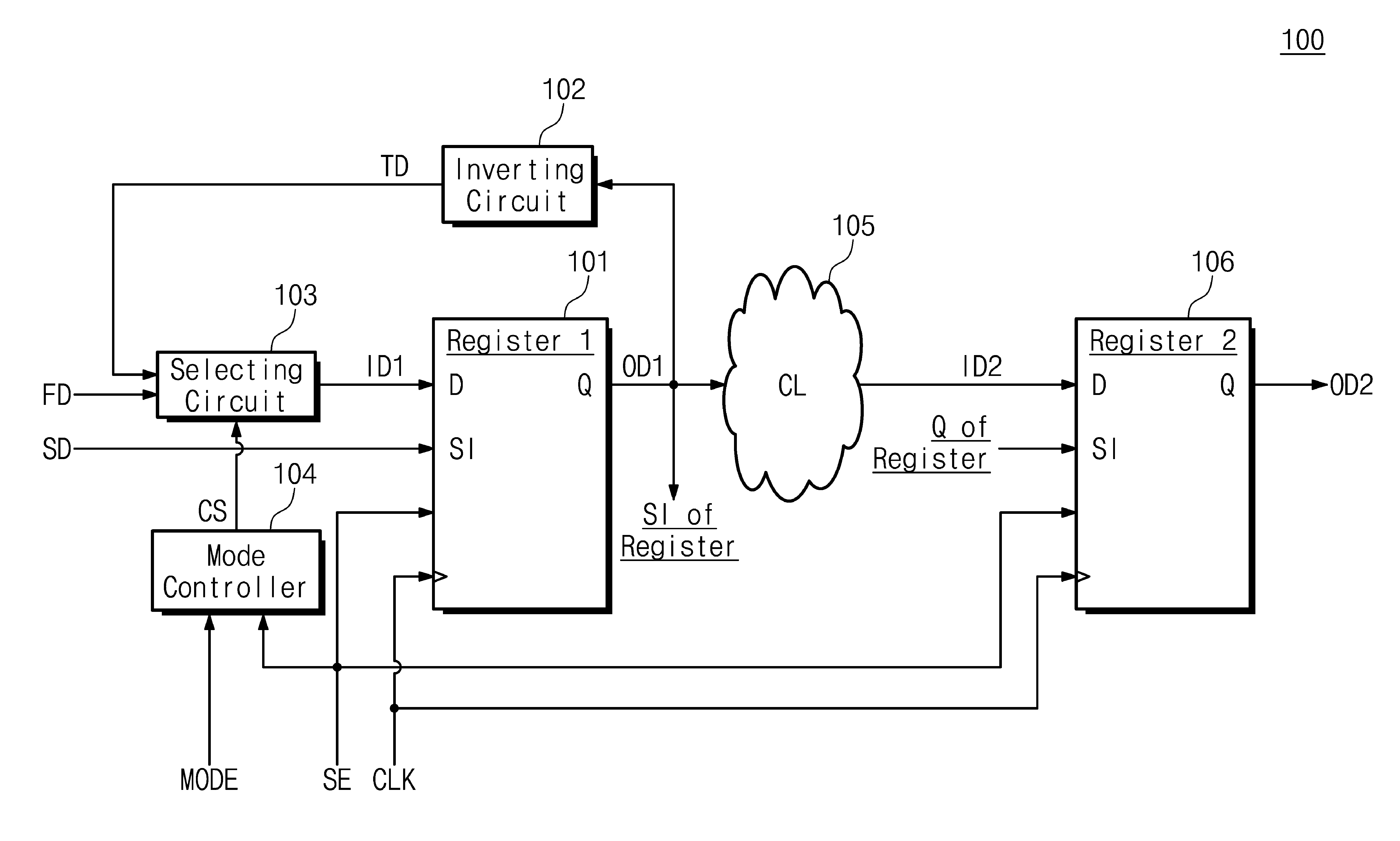
도 4는 본 발명의 하나의 실시 예에 따른 논리 회로의 AT-SPEED 테스트를 위한 SoC(100)를 보여주는 블록도이다. 도 4를 참조하면, SoC(100)는 제1 레지스터(101), 인버팅 회로(102), 선택 회로(103), 모드 컨트롤러(104), 논리 회로(105) 및 제2 레지스터(106)를 포함할 수 있다.Figure 4 is a block diagram showing the
제1 레지스터(101)는 제1 입력 데이터(ID1), 스캔 데이터(SD), 스캔 인에이블(SE) 및 클록(CLK)을 수신할 수 있다. 제1 레지스터(101)는 스캔 인에이블(SE) 및 클록(CLK)에 기초하여 제1 입력 데이터(ID1) 및 스캔 데이터(SD) 중 하나를 제1 출력 데이터(OD1)로서 출력할 수 있다. 도 2에서 설명된 바와 같이, 스캔 데이터(SD)는 입력 포트 또는 다른 레지스터를 통해 제1 레지스터(101)로 제공될 수 있다. 제1 출력 데이터(OD1)는 인버팅 회로(102), 논리 회로(105) 및 다른 레지스터의 입력 단자(SI)로 제공될 수 있다. 예를 들어, 제1 출력 데이터(OD1)는 제2 레지스터(106)의 입력 단자(SI)로 제공될 수 있다.The
인버팅 회로(102)는 제1 출력 데이터(OD1)를 반전시켜 테스트 데이터(TD)를 생성할 수 있다. 예를 들어, 제1 출력 데이터(OD1)의 값이 '1'인 경우, 테스트 데이터(TD)는 '0'일 수 있다. 인버팅 회로(102)로부터 출력되는 테스트 데이터(TD)는 선택 회로(103)로 제공될 수 있다. 예를 들어, 인버팅 회로(102)는 인버터로 구현될 수 있다. 그러나, 본 발명이 이에 한정되는 것은 아니며, 인버팅 회로(102)는 제1 출력 데이터(OD1)를 반전시킬 수 있는 임의의 회로 또는 임의의 회로들의 조합으로 구현될 수 있다.The inverting
선택 회로(103)는 테스트 데이터(TD) 및 기능 데이터(FD)를 수신할 수 있다. 선택 회로(103)는 선택 신호(CS)에 기초하여 테스트 데이터(TD) 및 기능 데이터(FD) 중 하나를 제1 입력 데이터(ID1)로서 출력할 수 있다. 기능 데이터(FD)는 입력 포트 또는 다른 레지스터의 출력 단자(Q)로부터 제공될 수 있다. 예를 들어, 기능 데이터(FD)를 기반으로 SoC(100)는 정상 기능을 수행할 수 있다. 예를 들어, 선택 회로(103)는 멀티플렉서로 구현될 수 있으나, 본 발명이 이에 한정되는 것은 아니다.
모드 컨트롤러(104)는 모드 신호(MODE) 및 스캔 인에이블(SE)을 수신할 수 있다. 모드 컨트롤러(104)는 모드 신호(MODE) 및 스캔 인에이블(SE)에 기초하여 선택 신호(CS)를 생성할 수 있다. 모드 신호(MODE)는 SoC(100)의 다양한 동작 모드들 중 하나를 나타낼 수 있다. 모드 신호(MODE)는 도 1의 탑 컨트롤러(111)로부터 제공될 수 있다. 예를 들어, 모드 신호(MODE)는 논리 회로(105)의 AT-SPEED 테스트를 위한 모드(이하, AT-SPEED 테스트 모드라 함)를 나타낼 수 있다.The
예를 들어, 모드 신호(MODE)가 논리 회로(105)의 AT-SPEED 테스트 모드를 나타내고, 스캔 인에이블(SE)이 논리 로우 값을 나타내는 경우, 모드 컨트롤러(104)는 선택 회로(103)가 테스트 데이터(TD)를 출력하도록 선택 신호(CS)를 생성할 수 있다. 이 경우, 테스트 데이터(TD)가 제1 입력 데이터(ID1)로서 제1 레지스터(101)에 제공될 수 있다. 제1 레지스터(101)는 스캔 인에이블(SE)의 논리 로우 값과 클록(CLK)에 기초하여 테스트 데이터(TD)를 저장하고, 테스트 데이터(TD)를 제1 출력 데이터(OD1)로서 출력할 수 있다.For example, if the mode signal (MODE) indicates the AT-SPEED test mode of the
논리 회로(105)는 제1 출력 데이터(OD1)를 기반으로 연산을 수행할 수 있다. 논리 회로(105)는 연산에 따라 생성된 데이터를 제2 입력 데이터(ID2)로서 제2 레지스터(106)로 제공할 수 있다.The
제2 레지스터(106)는 제2 입력 데이터(ID2), 스캔 인에이블(SE) 및 클록(CLK)을 수신할 수 있다. 제2 레지스터(106)의 입력 단자(SI)는 다른 레지스터의 출력 단자(Q)에 연결될 수 있다. 예를 들어, 제2 레지스터(106)의 입력 단자(SI)는 제1 레지스터(101)의 출력 단자(Q)에 연결될 수 있다. 제2 레지스터(106)는 스캔 인에이블(SE) 및 클록(CLK)에 기초하여 제2 입력 데이터(ID2) 및 입력 단자(SI)로 제공되는 데이터 중 하나를 제2 출력 데이터(OD2)로서 출력할 수 있다. 예를 들어, 입력 단자(SI)로 제공되는 데이터는 다른 레지스터를 통해 입력되는 스캔 데이터일 수 있다.The
제1 레지스터(101)와 제2 레지스터(106)는 동일한 코어에 포함될 수 있다. 예를 들어, 제1 레지스터(101)와 제2 레지스터(106)는 도 1의 제1 코어(120)에 포함될 수 있다. 또는, 제1 레지스터(101)와 제2 레지스터(106)는 각각 서로 다른 코어에 포함될 수 있다. 예를 들어, 제1 레지스터(101)는 도 1의 제1 코어(120)에 포함되고, 제2 레지스터(106)는 도 1의 최상위 레벨 코어(110)에 포함될 수 있다. 그러나, 본 발명이 이에 한정되는 것은 아니며, 제1 레지스터(101) 및 제2 레지스터(106) 각각은 SoC(100)의 임의의 코어에 포함될 수 있다. The
제1 레지스터(101)는 입력 래퍼 레지스터 또는 출력 래퍼 레지스터에 포함될 수 있다. 이 경우, 인버팅 회로(102) 및 선택 회로(103)는 입력 래퍼 레지스터 및 출력 래퍼 레지스터의 피드백 경로 상에 위치할 수 있다. 그러나, 본 발명이 이에 한정되는 것은 아니다.The
도 5는 본 발명의 실시 예에 따른 AT-SPEED 테스트를 위한 클록(CLK) 및 스캔 인에이블(SE)의 예시를 보여주는 타이밍도이다. 구체적으로, 논리 회로의 AT-SPEED 테스트를 위한 모드 신호(MODE)와 함께 도 5의 클록(CLK) 및 스캔 인에이블(SE)이 제공될 수 있다.Figure 5 is a timing diagram showing an example of clock (CLK) and scan enable (SE) for AT-SPEED test according to an embodiment of the present invention. Specifically, the clock (CLK) and scan enable (SE) of FIG. 5 may be provided along with the mode signal (MODE) for AT-SPEED testing of the logic circuit.
도 5를 참조하면, 가로축은 시간을 나타낸다. 논리 회로의 AT-SPEED 테스트는 제1 시프트 사이클, 캡쳐 사이클 및 제2 시프트 사이클을 기반으로 수행될 수 있다. 제1 시프트 사이클에서, 스캔 데이터가 레지스터들에 저장될 수 있다. 캡쳐 사이클에서, 저장된 스캔 데이터를 기반으로 논리 회로로부터 출력되는 결과 데이터가 레지스터들에 저장될 수 있다. 제2 시프트 사이클에서, 레지스터들에 저장된 결과 데이터가 출력될 수 있다. 출력되는 결과 데이터에 기초하여 논리 회로의 천이 지연 고장이 판별될 수 있다. 즉, 시프트 사이클에서는 스캔 경로를 따라 레지스터들을 통해 데이터가 순차적으로 전달될 수 있다. 캡쳐 사이클에서는 기능 경로를 따라 레지스터들에 저장된 데이터가 논리 회로를 통해 처리될 수 있다.Referring to Figure 5, the horizontal axis represents time. AT-SPEED testing of a logic circuit may be performed based on a first shift cycle, a capture cycle, and a second shift cycle. In the first shift cycle, scan data may be stored in registers. In the capture cycle, result data output from the logic circuit based on the stored scan data may be stored in registers. In the second shift cycle, the resulting data stored in the registers may be output. A transition delay failure of the logic circuit may be determined based on the output result data. That is, in a shift cycle, data can be sequentially transferred through registers along a scan path. In the capture cycle, data stored in registers along a functional path can be processed through logic circuits.
클록(CLK)은 시프트 사이클에서 제1 주파수를 가지고, 캡쳐 사이클에서 제2 주파수를 가질 수 있다. 이 경우, 제1 주파수는 제2 주파수보다 낮을 수 있다. 시프트 사이클은 레지스터들을 통해 데이터가 전달되는 구간(즉, 스캔 데이터가 레지스터들로 입력되거나 레지스터들에 저장된 결과 데이터가 출력되는 구간)이므로, 클록(CLK)의 주파수는 AT-SPEED 테스트에 영향을 주지 않을 수 있다. 이에 따라, 시프트 사이클에서 낮은 주파수를 갖도록 클록(CLK)이 생성될 수 있다. 이 경우, 저전력으로 스캔 데이터가 입력되고 결과 데이터가 출력될 수 있다. 캡쳐 사이클에서는 AT-SPEED 테스트를 위해 클록(CLK)의 주파수가 구동 클록(CLK)(즉, 정상 기능을 수행하기 위한 클록(CLK))의 주파수와 동일할 수 있다. 이에 따라, 캡쳐 사이클의 클록(CLK)에 기초하여 논리 회로의 AT-SPEED 테스트가 수행될 수 있다.The clock CLK may have a first frequency in a shift cycle and a second frequency in a capture cycle. In this case, the first frequency may be lower than the second frequency. Since the shift cycle is a section in which data is transferred through registers (i.e., a section in which scan data is input to registers or result data stored in registers is output), the frequency of the clock (CLK) does not affect the AT-SPEED test. It may not be possible. Accordingly, the clock CLK may be generated to have a low frequency in the shift cycle. In this case, scan data can be input and result data can be output with low power. In the capture cycle, for the AT-SPEED test, the frequency of the clock (CLK) may be the same as the frequency of the driving clock (CLK) (i.e., the clock (CLK) for performing normal functions). Accordingly, the AT-SPEED test of the logic circuit can be performed based on the clock (CLK) of the capture cycle.
도 5에는 클록(CLK)이 각각의 시프트 사이클에서 두 개의 펄스를 갖는 것으로 도시되었으나, 본 발명이 이에 한정되는 것은 아니다. 예를 들어, 각각의 시프트 사이클에서 클록(CLK)이 갖는 펄스의 개수는 스캔 데이터가 입력되는 레지스터들의 개수에 따라 달라질 수 있다.In FIG. 5, the clock CLK is shown as having two pulses in each shift cycle, but the present invention is not limited thereto. For example, the number of pulses of the clock CLK in each shift cycle may vary depending on the number of registers into which scan data is input.
이하에서는, 도 6을 참조하여 도 4의 SoC(100)의 동작을 상세하게 설명할 것이다. 설명의 편의를 위해, 제1 레지스터(101)의 출력 단자(Q)는 제2 레지스터(106)의 입력 단자(SI)에 연결되는 것으로 가정한다.Hereinafter, the operation of the
도 6은 도 5의 클록(CLK) 및 스캔 인에이블(SE)을 기반으로 도 4의 SoC(100)의 동작 예시를 설명하기 위한 도면이다. 도 5 및 도 6을 참조하면, 제1 시프트 사이클에서 제1 및 제2 레지스터들(101, 106)은 스캔 인에이블(SE)의 논리 하이 값에 응답하여 입력 단자(SI)로 입력되는 스캔 데이터를 선택할 수 있다. 제1 시간(t1)에서 제1 레지스터(101)로 제1 스캔 데이터(SD1)가 입력될 수 있다. 제1 레지스터(101)는 클록(CLK)의 상승 에지에 응답하여 제1 스캔 데이터(SD1)를 저장하고, 제1 출력 데이터(OD1)로서 제1 스캔 데이터(SD1)를 출력할 수 있다. 제1 스캔 데이터(SD1)는 제2 레지스터(106)의 입력 단자(SI)로 제공될 수 있다.FIG. 6 is a diagram for explaining an example of the operation of the
제2 시간(t2)에서 제1 레지스터(101)로 제2 스캔 데이터(SD2)가 입력될 수 있다. 제1 레지스터(101)는 클록(CLK)의 상승 에지에 응답하여 제2 스캔 데이터(SD2)를 저장하고, 제1 출력 데이터(OD1)로서 제2 스캔 데이터(SD2)를 출력할 수 있다. 제2 레지스터(106)는 클록(CLK)의 상승 에지에 응답하여 입력 단자(SI)로 입력되는 제1 스캔 데이터(SD1)를 저장할 수 있다. 제2 스캔 데이터(SD2)는 인버팅 회로(102)로 제공될 수 있다. 인버팅 회로(102)는 제2 스캔 데이터(SD2)를 반전시켜 테스트 데이터(TD)를 출력할 수 있다. 테스트 데이터(TD)는 선택 회로(103)로 제공될 수 있다.Second scan data SD2 may be input to the
선택 회로(103)는 테스트 데이터(TD) 및 기능 데이터(FD)를 수신할 수 있다. 선택 회로(103)는 제3 시간(t3) 전까지 모드 컨트롤러(104)로부터 제공되는 선택 신호(CS)에 따라 기능 데이터(FD)를 제1 입력 데이터(ID1)로서 출력할 수 있다. 제3 시간(t3)에서 모드 컨트롤러(104)는 모드 신호(MODE) 및 스캔 인에이블(SE)의 로우 값에 기초하여 선택 회로(103)로부터 테스트 데이터(TD)가 출력되도록 선택 신호(CS)를 생성할 수 있다. 여기서, 모드 신호(MODE)는 논리 회로(105)의 AT-SPEED 테스트 모드를 나타낼 수 있다. 이에 따라, 제3 시간(t3)에서 선택 회로(103)는 선택 신호(CS)에 응답하여 제1 입력 데이터(ID1)로서 테스트 데이터(TD)를 출력할 수 있다. 출력된 테스트 데이터(TD)는 제1 레지스터(101)의 입력 단자(D)로 입력될 수 있다.
캡쳐 사이클에서 제1 및 제2 레지스터들(101, 106)은 스캔 인에이블(SE)의 논리 로우 값에 기초하여 입력 단자(D)로 입력되는 입력 데이터를 선택할 수 있다. 제4 시간(t4)에서 제1 레지스터(101)는 클록(CLK)의 상승 에지에 응답하여 입력 단자(D)로 입력되는 테스트 데이터(TD)를 저장할 수 있다. 이에 따라, 테스트 데이터(TD)는 제1 출력 데이터(OD1)로서 출력될 수 있다. 테스트 데이터(TD)는 논리 회로(105)로 제공될 수 있다. 논리 회로(105)는 테스트 데이터(TD)를 기반으로 연산을 수행하고, 연산 결과로서 결과 데이터(RD)를 출력할 수 있다. 이에 따라, 제2 입력 데이터(ID2)로서 결과 데이터(RD)가 제2 레지스터(106)로 입력될 수 있다.In the capture cycle, the first and
제5 시간(t5)에서 제2 레지스터(106)는 클록(CLK)의 상승 에지에 응답하여 입력 단자(D)로 입력되는 결과 데이터(RD)를 저장할 수 있다. 제2 레지스터(106)는 제2 출력 데이터(OD2)로서 결과 데이터(RD)를 출력할 수 있다. 제2 시프트 사이클에서 제2 레지스터(106)에 저장된 결과 데이터(RD)가 스캔 경로를 따라 SoC(100)로부터 출력될 수 있다. 예를 들어, 제7 시간(t7) 및 제8 시간(t8)에서 결과 데이터(RD)는 스캔 경로 상의 레지스터들에 순차적으로 저장될 수 있다. 이와 같은 방식으로 결과 데이터(RD)는 출력 포트를 통해 SoC(100)로부터 출력될 수 있다.At the fifth time t5, the
출력된 결과 데이터(RD)의 값을 기반으로 논리 회로(105)의 천이 지연 고장이 판별될 수 있다. 예를 들어, 결과 데이터(RD)의 값이 원하는 값과 다른 경우, 논리 회로(105)의 천이 지연 고장이 존재하는 것으로 판별될 수 있다.A transition delay failure of the
테스트 데이터(TD)의 값이 제2 스캔 데이터(SD2)의 값과 동일한 경우, 논리 회로(105)로부터 출력되는 결과 데이터(RD)의 값이 동일하게 유지될 수 있다. 이 경우, 논리 회로(105)의 고착 고장과 천이 지연 고장이 구분되지 않을 수 있으므로, 논리 회로(105)의 AT-SPEED 테스트가 정확하게 수행되지 않을 수 있다. 따라서, 테스트 데이터(TD)는 제2 스캔 데이터(SD2)를 반전시켜 생성될 수 있다.When the value of the test data TD is the same as the value of the second scan data SD2, the value of the result data RD output from the
상술한 바와 같이, 제1 시프트 사이클에서 테스트 데이터(TD)가 제1 레지스터(101)로 전달될 수 있다. 캡쳐 사이클에서 클록(CLK)의 제1 펄스(P1)에 응답하여 테스트 데이터(TD)가 제1 레지스터(101)로부터 출력될 수 있다. 클록(CLK)의 제1 펄스(P1)를 바로 뒤따르는 클록(CLK)의 제2 펄스(P2)에 응답하여 제2 레지스터(106)가 결과 데이터(RD)를 저장할 수 있다. 즉, 제1 펄스(P1)의 상승 에지와 제2 펄스(P2) 의 상승 에지 사이의 구간에서 논리 회로(105)가 테스트 데이터(TD)를 기반으로 결과 데이터(RD)를 생성할 수 있다. 즉, 결과 데이터(RD)는 제4 시간(t4)과 제5 시간(t5) 사이의 구간에서 논리 회로(105)의 동작에 의해 생성될 수 있다. 캡쳐 사이클에서 클록(CLK)의 주파수는 정상 기능을 수행하기 위한 클록(CLK)의 주파수와 동일하므로, 제4 시간(t4)과 제5 시간(t5) 사이의 구간에서 논리 회로(105)의 동작에 의해 생성된 결과 데이터(RD)를 기반으로 논리 회로(105)의 AT-SPEED 테스트가 수행되는 경우, 논리 회로(105)의 천이 지연 고장이 판별될 수 있다.As described above, test data (TD) may be transferred to the
상술한 바와 같이, 본 발명의 실시 예에 따르면, 두 개의 레지스터들(101, 106)을 기반으로 논리 회로(105)의 AT-SPEED 테스트가 수행될 수 있다. 이 경우, 제1 레지스터(101)의 피드백 경로 상에 위치하는 인버팅 회로(102)는 제1 레지스터(101)로 데이터를 제공하는 논리 회로의 역할을 수행할 수 있다. 따라서, 논리 회로(105)의 AT-SPEED 테스트 시, 제1 레지스터(101)는 기능 경로 상의 두 개의 레지스터들의 역할을 수행할 수 있다.As described above, according to an embodiment of the present invention, an AT-SPEED test of the
도 7은 AT-SPEED 테스트를 위한 도 4의 SoC(100)의 동작의 예시를 보여주는 순서도이다. 도 4, 도 5 및 도 7을 참조하면, S101 단계에서, 제1 레지스터(101)는 제1 주파수를 가지는 클록(CLK)에 응답하여 스캔 데이터(SD)를 출력할 수 있다. S102 단계에서, 인버팅 회로(102)는 제1 레지스터(101)로부터 출력된 스캔 데이터(SD)를 반전시켜 생성된 테스트 데이터(TD)를 제1 레지스터(101)로 제공할 수 있다. 이 경우, 선택 회로(103)는 선택 신호(CS)에 기초하여 제1 입력 데이터(ID1)로서 테스트 데이터(TD)를 출력할 수 있다. 선택 회로(103)로부터 출력된 테스트 데이터(TD)가 제1 레지스터(101)로 제공될 수 있다.FIG. 7 is a flowchart showing an example of the operation of the
S103 단계에서, 제1 레지스터(101)는 제2 주파수를 가지는 클록(CLK)의 제1 펄스(P1)에 응답하여 테스트 데이터(TD)를 출력할 수 있다. 제1 레지스터(101)는 제1 출력 데이터(OD1)로서 테스트 데이터(TD)를 출력할 수 있다. S104 단계에서, 논리 회로(105)는 제1 레지스터(101)로부터 출력되는 테스트 데이터(TD)에 기초하여 결과 데이터를 출력할 수 있다. 논리 회로(105)는 제2 입력 데이터(ID2)로서 결과 데이터를 제2 레지스터(106)로 제공할 수 있다. S105 단계에서, 제2 레지스터(106)는 제2 주파수를 가지는 클록(CLK)의 제2 펄스(P2)에 응답하여 결과 데이터를 저장할 수 있다. 저장된 결과 데이터를 기반으로 논리 회로(105)의 천이 지연 고장이 판별될 수 있다.In step S103, the
이하에서는, 도 4의 제1 레지스터(101)가 입력 래퍼 레지스터 또는 출력 래퍼 레지스터에 포함되는 것으로 가정한다. 즉, 인버팅 회로(102) 및 선택 회로(103)는 입력 래퍼 레지스터 및 출력 래퍼 레지스터의 피드백 경로 상에 위치하는 것으로 가정한다. 이를 전제로, 도 8 내지 도 11을 참조하여 다양한 위치에 존재하는 논리 회로의 AT-SPEED 테스트를 위한 예시들이 설명될 것이다.Hereinafter, it is assumed that the
도 8은 본 발명의 하나의 실시 예에 따른 논리 회로(225)의 AT-SPEED 테스트를 위한 SoC(200)를 보여주는 블록도이다. 도 8을 참조하면, SoC(200)는 제1 코어(220)를 포함할 수 있다. 제1 코어(220)는, 도 1에서 설명된 바와 같이, SoC(200)의 하위 레벨 코어들 중 하나일 수 있다. 제1 코어(220)는 제1 레지스터(221), 인버팅 회로(222), 선택 회로(223), 모드 컨트롤러(224), 논리 회로(225), 제2 레지스터(226) 및 입력 포트(227)를 포함할 수 있다. 제1 레지스터(221), 인버팅 회로(222), 선택 회로(223), 모드 컨트롤러(224), 논리 회로(225) 및 제2 레지스터(226)는 도 4의 제1 레지스터(101), 인버팅 회로(102), 선택 회로(103), 모드 컨트롤러(104), 논리 회로(105) 및 제2 레지스터(106)와 실질적으로 동일 또는 유사하게 동작할 수 있으므로 자세한 설명은 생략된다.Figure 8 is a block diagram showing the
제1 레지스터(221)는 입력 포트(227)에 최 근접한 입력 래퍼 레지스터에 포함될 수 있다. 선택 회로(223)로 제공되는 기능 데이터(FD)는 입력 포트(227)를 통해 전달될 수 있다. 이 경우, 기능 데이터(FD)는 별개의 코어로부터 제공될 수 있다. 예를 들어, 기능 데이터(FD)는 최상위 레벨 코어 또는 다른 하위 레벨 코어로부터 제공될 수 있다.The
도 4 내지 도 6을 참조하여 설명된 바와 같이, 제1 및 제2 레지스터들(221, 226)을 기반으로 제1 레지스터(221)와 제2 레지스터(226) 사이에 위치하는 논리 회로(225)의 AT-SPEED 테스트가 수행될 수 있다. 이에 따라, 입력 래퍼 레지스터로부터 출력되는 출력 데이터를 처리하는 논리 회로의 AT-SPEED 테스트가 수행될 수 있다. As described with reference to FIGS. 4 to 6, a
도 9는 본 발명의 하나의 실시 예에 따른 논리 회로(325)의 AT-SPEED 테스트를 위한 SoC(300)를 보여주는 블록도이다. 도 9를 참조하면, SoC(300)는 최상위 레벨 코어(310) 및 제1 코어(320)를 포함할 수 있다. 제1 코어(320)는, 도 1에서 설명된 바와 같이, SoC(300)의 하위 레벨 코어들 중 하나일 수 있다. 최상위 레벨 코어(310)는 제2 레지스터(311) 및 입력 포트(312)를 포함할 수 있다. 제1 코어(320)는 제1 레지스터(321), 인버팅 회로(322), 선택 회로(323), 모드 컨트롤러(324), 논리 회로(325) 및 출력 포트(326)를 포함할 수 있다.Figure 9 is a block diagram showing the
제1 레지스터(321)는 출력 포트(326)에 최 근접한 출력 래퍼 레지스터에 포함될 수 있다. 제1 코어(320)의 출력 포트(326)는 최상위 레벨 코어(310)의 입력 포트(312)에 연결될 수 있다. 이 경우, 논리 회로(325)로부터 출력되는 데이터가 출력 포트(326) 및 입력 포트(312)를 통해 최상위 레벨 코어(310)의 제2 레지스터(311)로 전달될 수 있다. 즉, 제2 입력 데이터(ID2)로서 논리 회로(325)의 출력 데이터가 제공될 수 있다. 이와 같이 제1 레지스터(321) 및 제2 레지스터(311)는 하나의 기능 경로 상에 위치하므로, 제1 레지스터(321) 및 제2 레지스터(311)를 기반으로 논리 회로(325)의 AT-SPEED 테스트가 수행될 수 있다.The
도 5 및 도 9를 참조하면, 제2 시간(t2)에서, 제1 레지스터(321)는 클록(CLK)의 상승 에지에 응답하여 스캔 데이터(SD)를 저장할 수 있다. 제1 레지스터(321)는 제1 출력 데이터(OD1)로서 스캔 데이터(SD)를 출력할 수 있다. 인버팅 회로(322)는 제1 레지스터(321)로부터 출력된 스캔 데이터(SD)를 반전시켜 테스트 데이터(TD)를 생성할 수 있다. 테스트 데이터(TD)는 선택 회로(323)로 제공될 수 있다. Referring to FIGS. 5 and 9 , at a second time t2, the
제3 시간(t3)에서 모드 컨트롤러(324)는 모드 신호(MODE) 및 스캔 인에이블(SE)의 논리 로우 값에 기초하여 선택 회로(323)로부터 테스트 데이터(TD)가 출력되도록 선택 신호(CS)를 생성할 수 있다. 이 경우, 모드 신호(MODE)는 논리 회로(325)의 AT-SPEED 테스트 모드를 나타낼 수 있다. 선택 회로(323)는 선택 신호(CS)를 기반으로 기능 데이터(FD)와 테스트 데이터(TD) 중 테스트 데이터(TD)를 제1 입력 데이터(ID1)로서 출력할 수 있다. 즉, 제1 레지스터(321)의 입력 단자(D)로 테스트 데이터(TD)가 입력될 수 있다.At the third time (t3), the
제4 시간(t4)에서 제1 레지스터(321)는 클록(CLK)의 상승 에지에 응답하여 테스트 데이터(TD)를 제1 출력 데이터(OD1)로서 출력할 수 있다. 논리 회로(325)는 테스트 데이터(TD)를 기반으로 연산을 수행하고, 결과 데이터를 출력할 수 있다. 결과 데이터는 출력 포트(326) 및 입력 포트(312)를 통해 제2 입력 데이터(ID2)로서 제2 레지스터(311)로 제공될 수 있다. 제5 시간(t5)에서 제2 레지스터(311)는 클록(CLK)의 상승 에지에 응답하여 결과 데이터를 저장할 수 있다. 결과 데이터는 제2 출력 데이터(OD2)로서 출력될 수 있다. 이에 따라, 제2 출력 데이터(OD2)를 기반으로 논리 회로(325)의 천이 지연 고장이 판별될 수 있다.At the fourth time t4, the
상술한 바와 같이, 논리 회로(325)의 AT-SPEED 테스트가 수행되는 경우, 최상위 레벨 코어(310)와 제1 코어(320) 사이의 인터페이스의 AT-SPEED 테스트가 수행될 수 있다.As described above, when the AT-SPEED test of the
도 9에는 논리 회로(325)가 제1 코어(320)에 포함되는 것으로 도시되었으나, 본 발명은 이에 한정되지 않는다. 예를 들어, 논리 회로(325)는 최상위 레벨 코어(310)에 포함될 수 있다. 즉, 제1 레지스터(321) 및 제2 레지스터(311) 사이에 위치하는 논리 회로에 대한 AT-SPEED 테스트가 수행될 수 있다.Although the
도 10은 본 발명의 하나의 실시 예에 따른 논리 회로(414)의 AT-SPEED 테스트를 위한 SoC(400)를 보여주는 블록도이다. 도 10을 참조하면, SoC(400)는 최상위 레벨 코어(410) 및 제1 코어(420)를 포함할 수 있다. 제1 코어(420)는, 도 1에서 설명된 바와 같이, SoC(400)의 하위 레벨 코어들 중 하나일 수 있다. 최상위 레벨 코어(410)는 제1 레지스터(411), 제1 논리 회로(412), 제2 레지스터(413), 제2 논리 회로(414) 및 출력 포트(415)를 포함할 수 있다. 제1 코어(420)는 제3 레지스터(421), 인버팅 회로(422), 선택 회로(423), 모드 컨트롤러(424) 및 입력 포트(425)를 포함할 수 있다. 제2 논리 회로(414)의 AT-SPEED 테스트를 위해, 제1 논리 회로(412)의 결함이 존재하지 않는 것으로 가정한다.Figure 10 is a block diagram showing the
제3 레지스터(421)는 입력 포트(425)에 최 근접한 입력 래퍼 레지스터에 포함될 수 있다. 최상위 레벨 코어(410)의 출력 포트(415)는 제1 코어(420)의 입력 포트(425)에 연결될 수 있다. 이 경우, 제2 논리 회로(414)로부터 출력되는 데이터가 출력 포트(415) 및 입력 포트(425)를 통해 제1 코어(420)의 선택 회로(423)로 전달될 수 있다. 즉, 기능 데이터(FD)로서 제2 논리 회로(414)의 출력 데이터가 제공될 수 있다. 이와 같이 제1 레지스터(411), 제2 레지스터(413) 및 제3 레지스터(421)는 하나의 기능 경로 상에 위치할 수 있다. 이 경우, 제1 내지 제3 레지스터들(411, 413, 421)을 기반으로 제2 논리 회로(414)의 AT-SPEED 테스트가 수행될 수 있다.The
모드 신호(MODE)는 제2 논리 회로(414)의 AT-SPEED 테스트 모드를 나타낼 수 있다. 모드 컨트롤러(424)는 모드 신호(MODE)에 기초하여 선택 회로(423)가 기능 데이터(FD)를 출력하도록 선택 신호(CS)를 생성할 수 있다. 즉, 모드 컨트롤러(424)는 스캔 인에이블(SE)의 값과 관계없이 선택 회로(423)로부터 기능 데이터(FD)가 출력되도록 선택 신호(CS)를 생성할 수 있다. 즉, 제2 논리 회로(414)의 AT-SPEED 테스트를 위해, 인버팅 회로(422)로부터 출력되는 테스트 데이터(TD)가 이용되지 않을 수 있다.The mode signal MODE may represent the AT-SPEED test mode of the
도 5 및 도 10을 참조하면, 제2 시간(t2)에서, 제1 레지스터(411)는 클록(CLK)의 상승 에지에 응답하여 스캔 데이터(SD)를 저장할 수 있다. 제1 레지스터(411)는 제1 출력 데이터(OD1)로서 스캔 데이터(SD)를 출력할 수 있다. 제1 논리 회로(412)는 스캔 데이터(SD)를 기반으로 연산을 수행하고, 연산 결과를 출력할 수 있다. 즉, 제2 입력 데이터(ID2)로서 연산 결과가 제2 레지스터(413)의 입력 단자(D)로 제공될 수 있다.Referring to FIGS. 5 and 10 , at a second time t2, the
제4 시간(t4)에서 제2 레지스터(413)는 클록(CLK)의 상승 에지에 응답하여 연산 결과를 제2 출력 데이터(OD2)로서 출력할 수 있다. 제2 논리 회로(414)는 제2 출력 데이터(OD2)를 기반으로 연산을 수행하고, 결과 데이터를 출력할 수 있다. 결과 데이터는 출력 포트(415) 및 입력 포트(425)를 통해 기능 데이터(FD)로서 선택 회로(423)로 제공될 수 있다. 선택 회로(423)는 선택 신호(CS)에 응답하여 결과 데이터를 출력할 수 있다. 이에 따라, 제3 입력 데이터(ID3)로서 결과 데이터가 제3 레지스터(421)로 제공될 수 있다. At the fourth time t4, the
제5 시간(t5)에서 제3 레지스터(421)는 클록(CLK)의 상승 에지에 응답하여 결과 데이터를 저장할 수 있다. 결과 데이터는 제3 출력 데이터(OD3)로서 출력될 수 있다. 이에 따라, 제3 출력 데이터(OD3)를 기반으로 제2 논리 회로(414)의 천이 지연 고장이 판별될 수 있다.At the fifth time t5, the
상술한 바와 같이, 제2 논리 회로(414)의 AT-SPEED 테스트가 수행되는 경우, 최상위 레벨 코어(410)와 제1 코어(420) 사이의 인터페이스의 AT-SPEED 테스트가 수행될 수 있다.As described above, when the AT-SPEED test of the
도 10에는 제2 논리 회로(414)가 최상위 레벨 코어(410)에 포함되는 것으로 도시되었으나, 본 발명은 이에 한정되지 않는다. 예를 들어, 제2 논리 회로(414)는 제1 코어(420)에 포함될 수 있다. 즉, 제2 레지스터(413) 및 제3 레지스터(421) 사이에 위치하는 논리 회로에 대한 AT-SPEED 테스트가 수행될 수 있다.Although the
도 9 및 도 10에 도시된 바와 같이, 본 발명의 실시 예들에 따르면, 최상위 레벨 코어와 하위 레벨 코어 사이의 인터페이스에 대한 AT-SPEED 테스트가 용이하게 수행될 수 있다.As shown in FIGS. 9 and 10, according to embodiments of the present invention, an AT-SPEED test for the interface between the top level core and the lower level core can be easily performed.
도 11은 본 발명의 하나의 실시 예에 따른 논리 회로(525)의 AT-SPEED 테스트를 위한 SoC(500)를 보여주는 블록도이다. 도 11을 참조하면, SoC(500)는 제1 코어(520) 및 제2 코어(530)를 포함할 수 있다. 제1 및 제2 코어들(520, 530) 각각은, 도 1에서 설명된 바와 같이, SoC(500)의 하위 레벨 코어들 중 하나일 수 있다. 제1 코어(520)는 제1 레지스터(521), 제1 인버팅 회로(522), 제1 선택 회로(523), 제1 모드 컨트롤러(524), 논리 회로(525) 및 출력 포트(526)를 포함할 수 있다. 제2 코어(530)는 제2 레지스터(531), 제2 인버팅 회로(532), 제2 선택 회로(533), 제2 모드 컨트롤러(534) 및 입력 포트(535)를 포함할 수 있다.Figure 11 is a block diagram showing the
제1 레지스터(521)는 출력 포트(526)에 최 근접한 출력 래퍼 레지스터에 포함될 수 있다. 제2 레지스터(531)는 입력 포트(535)에 최 근접한 입력 래퍼 레지스터에 포함될 수 있다. 제1 코어(520)의 출력 포트(526)는 제2 코어(530)의 입력 포트(535)에 연결될 수 있다. 이 경우, 논리 회로(525)로부터 출력되는 데이터가 출력 포트(526) 및 입력 포트(535)를 통해 제2 코어(530)의 제2 선택 회로(533)로 전달될 수 있다. 즉, 제2 기능 데이터(FD2)로서 논리 회로(525)의 출력 데이터가 제공될 수 있다. 이와 같이 제1 레지스터(521) 및 제2 레지스터(531)는 하나의 기능 경로 상에 위치할 수 있다. 이 경우, 제1 및 제2 레지스터들(521, 531)을 기반으로 논리 회로(525)의 AT-SPEED 테스트가 수행될 수 있다.The
이 경우, 모드 신호(MODE)는 논리 회로(525)의 AT-SPEED 테스트 모드를 나타낼 수 있다. 제2 모드 컨트롤러(534)는 모드 신호(MODE)에 기초하여 제2 선택 회로(533)가 제2 기능 데이터(FD2)를 출력하도록 제2 선택 신호(CS2)를 생성할 수 있다. 즉, 제2 모드 컨트롤러(534)는 스캔 인에이블(SE)의 값과 관계없이 제2 선택 회로(533)로부터 제2 기능 데이터(FD2)가 출력되도록 제2 선택 신호(CS2)를 생성할 수 있다. 즉, 논리 회로(525)의 AT-SPEED 테스트를 위해, 제2 인버팅 회로(532)로부터 출력되는 제2 테스트 데이터(TD2)가 이용되지 않을 수 있다.In this case, the mode signal MODE may represent the AT-SPEED test mode of the
도 5 및 도 11을 참조하면, 제2 시간(t2)에서, 제1 레지스터(521)는 클록(CLK)의 상승 에지에 응답하여 스캔 데이터(SD)를 저장할 수 있다. 제1 레지스터(521)는 제1 출력 데이터(OD1)로서 스캔 데이터(SD)를 출력할 수 있다. 제1 인버팅 회로(522)는 제1 레지스터(521)로부터 출력된 스캔 데이터(SD)를 반전시켜 제1 테스트 데이터(TD1)를 생성할 수 있다. 제1 테스트 데이터(TD1)는 제1 선택 회로(523)로 제공될 수 있다.Referring to FIGS. 5 and 11 , at a second time t2, the
제3 시간(t3)에서 제1 모드 컨트롤러(524)는 모드 신호(MODE) 및 스캔 인에이블(SE)의 논리 로우 값에 기초하여 제1 선택 회로(523)로부터 제1 테스트 데이터(TD1)가 출력되도록 제1 선택 신호(CS1)를 생성할 수 있다. 제1 선택 회로(523)는 제1 선택 신호(CS1)를 기반으로 제1 테스트 데이터(TD1)를 제1 입력 데이터(ID1)로서 출력할 수 있다. 즉, 제1 레지스터(521)의 입력 단자(D)로 제1 테스트 데이터(TD1)가 입력될 수 있다.At the third time t3, the
제4 시간(t4)에서 제1 레지스터(521)는 클록(CLK)의 상승 에지에 응답하여 제1 테스트 데이터(TD1)를 제1 출력 데이터(OD1)로서 출력할 수 있다. 논리 회로(525)는 제1 테스트 데이터(TD1)를 기반으로 연산을 수행하고, 결과 데이터를 출력할 수 있다. 결과 데이터는 출력 포트(526) 및 입력 포트(535)를 통해 제2 기능 데이터(FD2)로서 제2 선택 회로(533)로 제공될 수 있다. 제2 선택 회로(533)는 제2 선택 신호(CS2)에 응답하여 결과 데이터를 출력할 수 있다. 이에 따라, 제2 입력 데이터(ID2)로서 결과 데이터가 제2 레지스터(531)로 제공될 수 있다. At the fourth time t4, the
제5 시간(t5)에서 제2 레지스터(531)는 클록(CLK)의 상승 에지에 응답하여 결과 데이터를 저장할 수 있다. 결과 데이터는 제2 출력 데이터(OD2)로서 출력될 수 있다. 이에 따라, 제2 출력 데이터(OD2)를 기반으로 논리 회로(525)의 천이 지연 고장이 판별될 수 있다.At the fifth time t5, the
상술한 바와 같이, 논리 회로(525)의 AT-SPEED 테스트가 수행되는 경우, 제1 코어(520)와 제2 코어(530) 사이의 인터페이스의 AT-SPEED 테스트가 수행될 수 있다. 즉, 본 발명의 실시 예들에 따르면, 하위 레벨 코어들 사이의 인터페이스에 대한 AT-SPEED 테스트가 용이하게 수행될 수 있다.As described above, when the AT-SPEED test of the
도 11에 도시된 바와 같이, 동일한 모드 신호(MODE)에 대하여 제1 모드 컨트롤러(524) 및 제2 모드 컨트롤러(534)는 다르게 동작할 수 있다. 모드 컨트롤러들(524, 534) 각각은 테스트 대상이 되는 논리 회로(525)의 위치에 따라 선택 신호(CS)를 생성할 수 있다. 예를 들어, 논리 회로(525)가 제1 선택 회로(523)를 기준으로 출력 데이터 경로 상에 위치하므로, 제1 모드 컨트롤러(524)는 제1 선택 회로(523)로부터 제1 테스트 데이터(TD1)가 출력되도록 제1 선택 신호(CS1)를 생성할 수 있다. 예를 들어, 논리 회로(525)가 제2 선택 회로(533)를 기준으로 입력 데이터 경로 상에 위치하므로, 제2 모드 컨트롤러(534)는 제2 선택 회로(533)로부터 제2 기능 데이터(FD2)가 출력되도록 제2 선택 신호(CS2)를 생성할 수 있다.As shown in FIG. 11, the
도 11에는 논리 회로(525)가 제1 코어(520)에 포함되는 것으로 도시되었으나, 본 발명은 이에 한정되지 않는다. 예를 들어, 논리 회로(525)는 제2 코어(530)에 포함될 수 있다. 즉, 제1 레지스터(521) 및 제2 레지스터(531) 사이에 위치하는 논리 회로에 대한 AT-SPEED 테스트가 수행될 수 있다.Although the
도 12는 본 발명의 하나의 실시 예에 따른 테스트 시스템(1000)을 보여주는 블록도이다. 도 12를 참조하면, 테스트 시스템(1000)은 테스트 장치(600) 및 SoC(700)를 포함할 수 있다. SoC(700)는 탑 컨트롤러(710) 및 논리 회로(720)를 포함할 수 있다.Figure 12 is a block diagram showing a
테스트 장치(600)는 SoC(700)의 논리 회로(720)에 대한 스캔 테스트를 수행하고, 논리 회로(720)의 결함을 판별할 수 있다. 스캔 테스트를 위해, 테스트 장치(600)는 스캔 데이터(SD)를 SoC(700)로 제공할 수 있다. 테스트 장치(600)는 스캔 데이터(SD)에 기초하여 SoC(700)로부터 출력된 결과 데이터(RD)를 수신할 수 있다. 이 경우, 결과 데이터(RD)는 스캔 데이터(SD)를 기반으로 논리 회로(720)로부터 출력된 데이터일 수 있다. 테스트 장치(600)는 결과 데이터(RD)를 기반으로 논리 회로(720)의 결함을 판별할 수 있다.The
논리 회로(720)에 대한 스캔 테스트를 위해, 테스트 장치(600)는 제어 신호들(CTRL)을 SoC(700)로 제공할 수 있다. 제어 신호들(CTRL)은 스캔 테스트를 위해 필요한 다양한 신호들을 포함할 수 있다. 예를 들어, 제어 신호들(CTRL)은 스캔 인에이블(SE), 클록(CLK), 테스트 대상에 대한 정보, 테스트 모드에 대한 정보 등을 포함할 수 있다. SoC(700)는 제어 신호들(CTRL)에 기초하여 논리 회로(720)를 테스트하기 위한 동작을 수행할 수 있다.For a scan test of the
탑 컨트롤러(710)는 제어 신호들(CTRL)을 기반으로 SoC(700) 내부의 회로들의 동작을 제어하기 위한 제어 신호들을 생성할 수 있다. 예를 들어, 탑 컨트롤러(710)는 논리 회로(720)의 테스트 모드를 나타내는 모드 신호(MODE)를 생성할 수 있다. 탑 컨트롤러(710)로부터 생성된 제어 신호들에 기초하여 논리 회로(720)를 테스트하기 위한 동작이 수행될 수 있다.The
예를 들어, 논리 회로(720)의 AT-SPEED 테스트를 위해, 테스트 장치(600)는 스캔 데이터(SD), 스캔 제어 신호들(CTRL)을 SoC(700)로 제공할 수 있다. 탑 컨트롤러(710)는 제어 신호들(CTRL)을 기반으로 모드 신호(MODE)를 생성할 수 있다. 이 경우, 모드 신호(MODE)는 논리 회로(720)의 AT-SPEED 테스트 모드를 나타낼 수 있다. 도 1 내지 도 11을 참조하여 설명된 바와 같이, 스캔 데이터(SD), 모드 신호(MODE), 스캔 인에이블(SE), 클록(CLK)을 기반으로 논리 회로(720)의 AT-SPEED 테스트가 수행될 수 있다. 이 경우, 논리 회로(720)의 위치에 관계 없이 논리 회로(720)의 AT-SPEED 테스트가 수행될 수 있다.For example, for an AT-SPEED test of the
도 13은 본 발명의 실시 예들에 따른 SoC가 적용된 전자 시스템(2000)의 예시적인 구성을 보여주는 블록도이다.Figure 13 is a block diagram showing an example configuration of an
전자 시스템(2000)은 메인 프로세서(2100), 워킹 메모리(2200), 스토리지 장치(2300), 프로세싱 장치(2400), 유저 인터페이스(2500) 및 버스(2600)를 포함할 수 있다. 예를 들어, 전자 시스템(2000)은 데스크톱 컴퓨터, 랩톱 컴퓨터, 태블릿 컴퓨터, 스마트 폰, 웨어러블 장치, 전기 자동차, 워크스테이션 등과 같은 전자 장치들 중 하나일 수 있다. 예를 들어, 전자 시스템(2000)은 최종 사용자(End-user)에 의해 이용되는 전자 장치일 수 있다. 또는, 전자 시스템(2000)은 서버 시스템, 데이터 센터 등과 같은 대규모 시스템의 구성 요소일 수 있다.The
메인 프로세서(2100)는 전자 시스템(2000)의 전반적인 동작들을 제어할 수 있다. 메인 프로세서(2100)는 다양한 종류의 산술 연산들 및/또는 논리 연산들을 수행할 수 있다. 도 1 내지 도 12를 참조하여 설명된 바와 같이, 메인 프로세서(2100)는 복수의 코어들이 포함된 SoC 형태로 구현될 수 있다. 이 경우, 메인 프로세서(2100)의 논리 회로에 대한 AT-SPEED 테스트가 용이하게 수행될 수 있다.The
워킹 메모리(2200)는 전자 시스템(2000)의 동작에 이용되는 데이터를 저장할 수 있다. 예시적으로, 워킹 메모리(2200)는 메인 프로세서(2100)에 의해 처리된 또는 처리될 데이터를 일시적으로 저장할 수 있다. 예를 들어, 워킹 메모리(2200)는 DRAM(Dynamic RAM), SDRAM(Synchronous RAM) 등과 같은 휘발성 메모리, 및/또는 PRAM(Phase-change RAM), MRAM(Magneto-resistive RAM), ReRAM(Resistive RAM), FRAM(Ferro-electric RAM) 등과 같은 불휘발성 메모리를 포함할 수 있다.The working
스토리지 장치(2300)는 전력 공급에 관계없이 데이터를 저장할 수 있다. 예를 들어, 스토리지 장치(1300)는 플래시 메모리, PRAM, MRAM, ReRAM, FRAM 등과 같은 불휘발성 메모리를 포함할 수 있다. 예를 들어, 스토리지 장치(2300)는 HDD(Hard Disk Drive), SSD(Solid State Drive), 카드 스토리지, 임베디드(Embedded) 스토리지 등과 같은 스토리지 매체를 포함할 수 있다.The
프로세싱 장치(2400)는 메인 프로세서(2100)의 제어 하에서 수신된 데이터를 처리할 수 있다. 프로세싱 장치(2400)는 다양한 연산을 통해 수신된 데이터를 처리할 수 있다. 프로세싱 장치(2400)는 처리된 데이터를 메인 프로세서(2100)로 제공할 수 있다. 즉, 프로세싱 장치(2400)는 특정 연산에 특화된 전용 프로세서일 수 있다. 예를 들어, 프로세싱 장치(2400)는 그래픽 처리 장치(GPU), 뉴럴 프로세싱 장치(NPU), 디지털 신호 처리 장치(DSP) 등으로 구현될 수 있다. 도 1 내지 도 12를 참조하여 설명된 바와 같이, 프로세싱 장치(2400)는 복수의 코어들이 포함된 SoC 형태로 구현될 수 있다. 이 경우, 프로세싱 장치(2400)의 논리 회로에 대한 AT-SPEED 테스트가 용이하게 수행될 수 있다.The
유저 인터페이스(2500)는 사용자와 전자 시스템(2000) 사이의 통신을 중재할 수 있다. 예를 들어, 유저 인터페이스(2500)는 키보드, 마우스, 키패드, 버튼, 터치 패널, 터치 스크린, 터치 패드, 터치 볼, 카메라, 마이크, 자이로스코프 센서, 진동 센서 등과 같은 입력 인터페이스를 포함할 수 있다. 예를 들어, 유저 인터페이스(2500)는 LCD(Liquid Crystal Display) 장치, LED(Light Emitting Diode) 표시 장치, OLED(Organic LED) 표시 장치, AMOLED(Active Matrix OLED) 표시 장치, 스피커, 모터 등과 같은 출력 인터페이스를 포함할 수 있다.
버스(2600)는 전자 시스템(2000)의 구성 요소들 사이에서 통신 경로를 제공할 수 있다. 전자 시스템(2000)의 구성 요소들은 버스(2600)의 버스 포맷에 기초하여 서로 데이터를 교환할 수 있다. 예를 들어, 버스 포맷은 USB, SCSI(Small Computer System Interface), PCIe(Peripheral Component Interconnect Express), M-PCIe(Mobile PCIe), ATA(Advanced Technology Attachment), PATA(Parallel ATA), SATA(Serial ATA), SAS(Serial Attached SCSI), IDE(Integrated Drive Electronics), EIDE(Enhanced IDE), NVMe(Nonvolatile Memory Express), UFS(Universal Flash Storage) 등과 같은 다양한 인터페이스 규약 중 하나 이상을 포함할 수 있다.
상술된 내용은 본 발명을 실시하기 위한 구체적인 실시 예들이다. 본 발명은 상술된 실시 예들뿐만 아니라, 단순하게 설계 변경되거나 용이하게 변경할 수 있는 실시 예들 또한 포함할 것이다. 또한, 본 발명은 실시 예들을 이용하여 용이하게 변형하여 실시할 수 있는 기술들도 포함될 것이다. 따라서, 본 발명의 범위는 상술된 실시 예들에 국한되어 정해져서는 안되며 후술하는 특허청구범위뿐만 아니라 이 발명의 특허청구범위와 균등한 것들에 의해 정해져야 할 것이다.The above-described details are specific embodiments for carrying out the present invention. The present invention will include not only the above-described embodiments, but also embodiments that can be simply changed or easily changed in design. In addition, the present invention will also include technologies that can be easily modified and implemented using the embodiments. Therefore, the scope of the present invention should not be limited to the above-described embodiments, but should be determined by the claims and equivalents of the present invention as well as the claims described later.
100: 시스템-온-칩
101: 제1 레지스터
102: 인버팅 회로
103: 선택 회로
104: 모드 컨트롤러
105: 논리 회로
106: 제2 레지스터
110: 최상위 레벨 코어
120: 코어100: System-on-Chip
101: first register
102: Inverting circuit
103: selection circuit
104: Mode controller
105: logic circuit
106: second register
110: Top level core
120: core
Claims (20)
상기 복수의 코어들 중 제1 코어에 포함되고, 상기 제1 코어의 입력 포트에 최 근접한 제1 스캔 레지스터;
상기 제1 스캔 레지스터의 피드백 경로 상에 위치하는 인버팅 회로;
상기 제1 코어에 포함되는 제2 스캔 레지스터; 및
상기 제1 스캔 레지스터 및 상기 제2 스캔 레지스터 사이의 데이터 경로 상에 위치하는 논리 회로를 포함하고,
상기 논리 회로의 AT-SPEED 테스트를 위한 테스트 모드에서,
상기 인버팅 회로는 상기 제1 스캔 레지스터로부터 출력된 스캔 데이터를 반전시켜 테스트 데이터를 생성하고,
상기 제1 스캔 레지스터는 클록의 제1 펄스에 응답하여 상기 테스트 데이터를 저장하고,
상기 논리 회로는 상기 제1 스캔 레지스터로부터 출력되는 상기 테스트 데이터에 기초하여 결과 데이터를 출력하고,
상기 제2 스캔 레지스터는 상기 클록의 제2 펄스에 응답하여 상기 결과 데이터를 저장하는 시스템-온-칩.In a system-on-chip including a plurality of cores,
a first scan register included in a first core among the plurality of cores and closest to an input port of the first core;
an inverting circuit located on a feedback path of the first scan register;
a second scan register included in the first core; and
Comprising a logic circuit located on a data path between the first scan register and the second scan register,
In the test mode for AT-SPEED testing of the logic circuit,
The inverting circuit generates test data by inverting scan data output from the first scan register,
the first scan register stores the test data in response to a first pulse of a clock,
The logic circuit outputs result data based on the test data output from the first scan register,
The second scan register stores the result data in response to a second pulse of the clock.
상기 제2 펄스는 상기 제1 펄스에 바로 뒤따르는 시스템-온-칩.According to claim 1,
System-on-chip, wherein the second pulse immediately follows the first pulse.
상기 클록의 주파수는 상기 시스템-온-칩의 정상 기능(normal function)을 위한 구동 클록의 주파수와 동일한 시스템-온-칩.According to claim 1,
A system-on-chip wherein the frequency of the clock is the same as the frequency of a driving clock for normal function of the system-on-chip.
상기 제2 스캔 레지스터에 저장된 상기 결과 데이터를 기반으로 상기 논리 회로의 천이 지연 고장이 판별되는 시스템-온-칩.According to claim 1,
A system-on-chip wherein a transition delay failure of the logic circuit is determined based on the result data stored in the second scan register.
상기 입력 포트로부터 출력되는 기능 데이터와 상기 인버팅 회로로부터 출력되는 상기 테스트 데이터 중 하나를 상기 제1 스캔 레지스터로 제공하도록 구성된 선택 회로를 더 포함하고,
상기 테스트 모드에서, 상기 선택 회로는 상기 테스트 데이터를 상기 제1 스캔 레지스터로 제공하는 시스템-온-칩.According to claim 1,
Further comprising a selection circuit configured to provide one of the function data output from the input port and the test data output from the inverting circuit to the first scan register,
In the test mode, the selection circuit provides the test data to the first scan register.
상기 기능 데이터는 상기 복수의 코어들 중 최상위 레벨 코어로부터 제공되는 시스템-온-칩.According to claim 5,
System-on-chip, wherein the functional data is provided from a highest level core among the plurality of cores.
상기 복수의 코어들 중 제1 코어에 포함되고, 상기 제1 코어의 출력 포트에 최 근접한 제1 스캔 레지스터;
상기 제1 스캔 레지스터의 피드백 경로 상에 위치하는 제1 인버팅 회로;
상기 복수의 코어들 중 제2 코어에 포함되는 제2 스캔 레지스터; 및
상기 제1 스캔 레지스터 및 상기 제2 스캔 레지스터 사이의 데이터 경로 상에 위치하는 논리 회로를 포함하고,
상기 논리 회로의 AT-SPEED 테스트를 위한 테스트 모드에서,
상기 제1 인버팅 회로는 상기 제1 스캔 레지스터로부터 출력된 스캔 데이터를 반전시켜 제1 테스트 데이터를 생성하고,
상기 제1 스캔 레지스터는 클록의 제1 펄스에 응답하여 상기 제1 테스트 데이터를 저장하고,
상기 논리 회로는 상기 제1 스캔 레지스터로부터 출력되는 상기 제1 테스트 데이터에 기초하여 결과 데이터를 출력하고,
상기 제2 스캔 레지스터는 상기 클록의 제2 펄스에 응답하여 상기 결과 데이터를 저장하는 시스템-온-칩.In a system-on-chip including a plurality of cores,
a first scan register included in a first core among the plurality of cores and closest to an output port of the first core;
a first inverting circuit located on a feedback path of the first scan register;
a second scan register included in a second core among the plurality of cores; and
Comprising a logic circuit located on a data path between the first scan register and the second scan register,
In the test mode for AT-SPEED testing of the logic circuit,
The first inverting circuit generates first test data by inverting scan data output from the first scan register,
the first scan register stores the first test data in response to a first pulse of a clock,
The logic circuit outputs result data based on the first test data output from the first scan register,
The second scan register stores the result data in response to a second pulse of the clock.
상기 제2 펄스는 상기 제1 펄스에 바로 뒤따르는 시스템-온-칩.According to claim 7,
System-on-chip, wherein the second pulse immediately follows the first pulse.
상기 클록의 주파수는 상기 시스템-온-칩의 정상 기능을 위한 구동 클록의 주파수와 동일한 시스템-온-칩.According to claim 7,
A system-on-chip wherein the frequency of the clock is the same as the frequency of a driving clock for normal functioning of the system-on-chip.
상기 제2 스캔 레지스터에 저장된 상기 결과 데이터를 기반으로 상기 논리 회로의 천이 지연 고장이 판별되는 시스템-온-칩.According to claim 7,
A system-on-chip wherein a transition delay failure of the logic circuit is determined based on the result data stored in the second scan register.
기능 데이터와 상기 제1 인버팅 회로로부터 출력되는 상기 제1 테스트 데이터를 수신하고, 상기 기능 데이터와 상기 제1 테스트 데이터 중 하나를 상기 제1 스캔 레지스터로 제공하도록 구성된 제1 선택 회로를 더 포함하고,
상기 테스트 모드에서, 상기 제1 선택 회로는 상기 제1 테스트 데이터를 상기 제1 스캔 레지스터로 제공하는 시스템-온-칩.According to claim 7,
Further comprising a first selection circuit configured to receive functional data and the first test data output from the first inverting circuit, and provide one of the functional data and the first test data to the first scan register; ,
In the test mode, the first selection circuit provides the first test data to the first scan register.
상기 제2 스캔 레지스터의 피드백 경로 상에 위치하는 제2 인버팅 회로; 및
상기 결과 데이터와 상기 제2 인버팅 회로로부터 출력되는 제2 테스트 데이터 중 하나를 상기 제2 스캔 레지스터로 제공하도록 구성된 제2 선택 회로를 더 포함하고,
상기 테스트 모드에서, 상기 제2 선택 회로는 상기 결과 데이터를 상기 제2 스캔 레지스터로 제공하는 시스템-온-칩.According to claim 11,
a second inverting circuit located on a feedback path of the second scan register; and
Further comprising a second selection circuit configured to provide one of the result data and second test data output from the second inverting circuit to the second scan register,
In the test mode, the second selection circuit provides the result data to the second scan register.
상기 제2 코어는 최상위 레벨 코어인 시스템-온-칩.According to claim 7,
The second core is a system-on-chip, which is the highest level core.
상기 제1 스캔 레지스터가 제1 주파수를 갖는 클록에 응답하여 스캔 데이터를 출력하는 단계;
상기 제1 스캔 레지스터로부터 출력되는 상기 스캔 데이터를 반전시켜 생성된 테스트 데이터를 상기 제1 스캔 레지스터로 제공하는 단계;
상기 제1 스캔 레지스터가 제2 주파수를 갖는 상기 클록의 제1 펄스에 응답하여 상기 테스트 데이터를 출력하는 단계;
상기 논리 회로가 상기 제1 스캔 레지스터로부터 출력되는 상기 테스트 데이터에 기초하여 결과 데이터를 출력하는 단계; 및
상기 제2 스캔 레지스터가 상기 제2 주파수를 갖는 상기 클록의 제2 펄스에 응답하여 상기 결과 데이터를 저장하는 단계를 포함하는 동작 방법.In a system-on-chip operating method for AT-SPEED testing of a logic circuit located on a data path between a first scan register and a second scan register,
outputting scan data from the first scan register in response to a clock having a first frequency;
providing test data generated by inverting the scan data output from the first scan register to the first scan register;
outputting, by the first scan register, the test data in response to a first pulse of the clock having a second frequency;
outputting result data by the logic circuit based on the test data output from the first scan register; and
and the second scan register storing the result data in response to a second pulse of the clock having the second frequency.
상기 제2 펄스는 상기 제1 펄스에 바로 뒤따르는 동작 방법.According to claim 14,
The second pulse immediately follows the first pulse.
상기 제2 주파수는 상기 시스템-온-칩의 정상 기능을 위한 구동 클록의 주파수와 동일한 동작 방법.According to claim 14,
The second frequency is the same as the frequency of a driving clock for normal functioning of the system-on-chip.
상기 제2 스캔 레지스터에 저장된 상기 결과 데이터를 기반으로 상기 논리 회로의 천이 지연 고장이 판별되는 동작 방법.According to claim 14,
An operation method in which a transition delay failure of the logic circuit is determined based on the result data stored in the second scan register.
상기 시스템-온-칩은 제1 입력 포트 및 제1 출력 포트를 포함하는 제1 코어 및 제2 입력 포트 및 제2 출력 포트를 포함하는 제2 코어를 포함하고,
상기 제1 출력 포트는 상기 제2 입력 포트에 연결되는 동작 방법.According to claim 14,
The system-on-chip includes a first core including a first input port and a first output port and a second core including a second input port and a second output port,
An operating method wherein the first output port is connected to the second input port.
상기 제1 스캔 레지스터 및 상기 제2 스캔 레지스터는 상기 제1 코어에 포함되고,
상기 제1 스캔 레지스터는 상기 제1 입력 포트에 최 근접한 입력 래퍼(wrapper) 레지스터인 동작 방법.According to claim 18,
The first scan register and the second scan register are included in the first core,
An operating method wherein the first scan register is an input wrapper register closest to the first input port.
상기 제1 스캔 레지스터는 상기 제1 코어에 포함되고,
상기 제2 스캔 레지스터는 상기 제2 코어에 포함되고,
상기 제1 스캔 레지스터는 상기 제1 출력 포트에 최 근접한 출력 래퍼 레지스터이고,
상기 제2 스캔 레지스터는 상기 제2 입력 포트에 최 근접한 입력 래퍼 레지스터인 동작 방법.According to claim 18,
The first scan register is included in the first core,
The second scan register is included in the second core,
The first scan register is an output wrapper register closest to the first output port,
The operating method wherein the second scan register is an input wrapper register closest to the second input port.
Priority Applications (5)
| Application Number | Priority Date | Filing Date | Title |
|---|---|---|---|
| KR1020190003372A KR102681969B1 (en) | 2019-01-10 | 2019-01-10 | System-on-chip for at-speed test of logic circuit and operating method thereof |
| US16/544,160 US10969432B2 (en) | 2019-01-10 | 2019-08-19 | System-on-chip for at-speed test of logic circuit and operating method thereof |
| DE102019124122.7A DE102019124122A1 (en) | 2019-01-10 | 2019-09-09 | One-chip system for an at-speed test of a logic circuit and operating method of the same |
| CN201911232389.1A CN111426946B (en) | 2019-01-10 | 2019-12-05 | System chip for full-speed testing of logic circuits and operation method thereof |
| US17/206,288 US11442107B2 (en) | 2019-01-10 | 2021-03-19 | System-on-chip for AT-SPEED test of logic circuit and operating method thereof |
Applications Claiming Priority (1)
| Application Number | Priority Date | Filing Date | Title |
|---|---|---|---|
| KR1020190003372A KR102681969B1 (en) | 2019-01-10 | 2019-01-10 | System-on-chip for at-speed test of logic circuit and operating method thereof |
Publications (2)
| Publication Number | Publication Date |
|---|---|
| KR20200087375A KR20200087375A (en) | 2020-07-21 |
| KR102681969B1 true KR102681969B1 (en) | 2024-07-08 |
Family
ID=71131943
Family Applications (1)
| Application Number | Title | Priority Date | Filing Date |
|---|---|---|---|
| KR1020190003372A Active KR102681969B1 (en) | 2019-01-10 | 2019-01-10 | System-on-chip for at-speed test of logic circuit and operating method thereof |
Country Status (4)
| Country | Link |
|---|---|
| US (2) | US10969432B2 (en) |
| KR (1) | KR102681969B1 (en) |
| CN (1) | CN111426946B (en) |
| DE (1) | DE102019124122A1 (en) |
Families Citing this family (11)
| Publication number | Priority date | Publication date | Assignee | Title |
|---|---|---|---|---|
| KR102681969B1 (en) * | 2019-01-10 | 2024-07-08 | 삼성전자주식회사 | System-on-chip for at-speed test of logic circuit and operating method thereof |
| US11531061B2 (en) | 2020-08-03 | 2022-12-20 | Qualcomm Incorporated | Interleaved testing of digital and analog subsystems with on-chip testing interface |
| CN112345924B (en) * | 2020-10-30 | 2024-09-03 | 上海兆芯集成电路股份有限公司 | Scan chain control circuit |
| CN114690028B (en) * | 2020-12-31 | 2025-05-30 | 蒂普爱可斯有限公司 | System on chip and method for testing components in a system at runtime |
| CN114002577B (en) * | 2021-10-21 | 2025-01-28 | 山东云海国创云计算装备产业创新中心有限公司 | Chip testing method, device, equipment and readable storage medium |
| CN114296510B (en) * | 2022-01-05 | 2024-05-07 | 深圳国微福芯技术有限公司 | On-chip clock controller |
| WO2023192671A1 (en) * | 2022-04-01 | 2023-10-05 | Google Llc | Custom wrapper cell for hardware testing |
| CN114994507A (en) * | 2022-05-31 | 2022-09-02 | 芯盟科技有限公司 | Control circuit for controlling logic turnover rate through clock tree node switch |
| CN115236493B (en) * | 2022-07-28 | 2023-07-21 | 摩尔线程智能科技(北京)有限责任公司 | DFT test circuit, test system and test method |
| CN118412347A (en) * | 2023-01-29 | 2024-07-30 | 华为技术有限公司 | A circuit and a computing device |
| TWI873965B (en) * | 2023-11-09 | 2025-02-21 | 瑞昱半導體股份有限公司 | Chip and chip testing method |
Citations (6)
| Publication number | Priority date | Publication date | Assignee | Title |
|---|---|---|---|---|
| WO2002001719A2 (en) | 2000-06-29 | 2002-01-03 | Logicvision, Inc. | Method and apparatus for testing high performance circuits |
| US20020138801A1 (en) | 2001-03-01 | 2002-09-26 | Laung-Terng Wang | Method and apparatus for diagnosing failures in an integrated circuit using design-for-debug (DFD) techniques |
| WO2007069097A1 (en) | 2005-11-02 | 2007-06-21 | Nxp B.V. | Ic testing methods and apparatus |
| US20140181605A1 (en) | 2012-03-25 | 2014-06-26 | Hanmanth R. Lingannagari | Asynchronous programmable jtag-based interface to debug any system-on-chip states, power modes, resets, clocks, and complex digital logic |
| US20140229778A1 (en) | 2013-02-14 | 2014-08-14 | Lsi Corporation | At-speed scan testing of interface functional logic of an embedded memory or other circuit core |
| US20180367128A1 (en) | 2017-06-16 | 2018-12-20 | International Business Machines Corporation | Increasing resolution of on-chip timing uncertainty measurements |
Family Cites Families (19)
| Publication number | Priority date | Publication date | Assignee | Title |
|---|---|---|---|---|
| JP2768910B2 (en) * | 1995-02-27 | 1998-06-25 | 日本モトローラ株式会社 | Scan test circuit in semiconductor integrated device |
| US7007213B2 (en) | 2001-02-15 | 2006-02-28 | Syntest Technologies, Inc. | Multiple-capture DFT system for detecting or locating crossing clock-domain faults during self-test or scan-test |
| DE60309761T2 (en) * | 2002-02-11 | 2007-10-11 | Texas Instruments Inc., Dallas | Method and apparatus for testing high speed interconnect circuits |
| US7194669B2 (en) | 2003-02-14 | 2007-03-20 | Logicvision, Inc. | Method and circuit for at-speed testing of scan circuits |
| KR20050060865A (en) * | 2003-12-17 | 2005-06-22 | 한국전자통신연구원 | Integrated circuit apparatus and method capable of scan testing intellectual property core in the system on chip for detecting the short of signal terminals and the normal operation of the core |
| EP1571456A1 (en) | 2004-03-01 | 2005-09-07 | Koninklijke Philips Electronics N.V. | Test circuit and method for hierarchical core |
| US20060181427A1 (en) | 2005-01-31 | 2006-08-17 | Csi Technology, Inc. | Machine condition indication system |
| US7487419B2 (en) | 2005-06-15 | 2009-02-03 | Nilanjan Mukherjee | Reduced-pin-count-testing architectures for applying test patterns |
| US7793179B2 (en) | 2006-06-27 | 2010-09-07 | Silicon Image, Inc. | Test clock control structures to generate configurable test clocks for scan-based testing of electronic circuits using programmable test clock controllers |
| JP5181499B2 (en) | 2007-03-07 | 2013-04-10 | 株式会社リコー | SCAN test circuit and semiconductor integrated circuit |
| US7831877B2 (en) * | 2007-03-08 | 2010-11-09 | Silicon Image, Inc. | Circuitry to prevent peak power problems during scan shift |
| JP5014907B2 (en) * | 2007-07-17 | 2012-08-29 | ルネサスエレクトロニクス株式会社 | Semiconductor memory device and test method thereof |
| CN101788644B (en) * | 2009-12-30 | 2011-11-16 | 龙芯中科技术有限公司 | Device and method for testing system-on-chip chip with multiple isomorphic IP cores |
| KR20110136531A (en) | 2010-06-15 | 2011-12-21 | 단국대학교 산학협력단 | Low-area wrapper cell for parallel testing of hierarchical SOC |
| US9140754B2 (en) * | 2011-02-28 | 2015-09-22 | Texas Instruments Incorporated | Scan-based MCM interconnecting testing |
| US9234942B2 (en) * | 2012-09-21 | 2016-01-12 | Apple Inc. | Transition fault testing of source synchronous interface |
| US9366724B1 (en) * | 2014-12-11 | 2016-06-14 | Freescale Semiconductor, Inc. | Scan testing with staggered clocks |
| KR102067198B1 (en) | 2017-06-30 | 2020-01-15 | 농업회사법인 주식회사 생생초 | Method for producing Geomgangsong lactic acid bacteria fermented beverage using Geomgangsong pine lactic acid bacteria fermented solution with enhanced GABA component |
| KR102681969B1 (en) * | 2019-01-10 | 2024-07-08 | 삼성전자주식회사 | System-on-chip for at-speed test of logic circuit and operating method thereof |
-
2019
- 2019-01-10 KR KR1020190003372A patent/KR102681969B1/en active Active
- 2019-08-19 US US16/544,160 patent/US10969432B2/en active Active
- 2019-09-09 DE DE102019124122.7A patent/DE102019124122A1/en active Pending
- 2019-12-05 CN CN201911232389.1A patent/CN111426946B/en active Active
-
2021
- 2021-03-19 US US17/206,288 patent/US11442107B2/en active Active
Patent Citations (7)
| Publication number | Priority date | Publication date | Assignee | Title |
|---|---|---|---|---|
| WO2002001719A2 (en) | 2000-06-29 | 2002-01-03 | Logicvision, Inc. | Method and apparatus for testing high performance circuits |
| US20020138801A1 (en) | 2001-03-01 | 2002-09-26 | Laung-Terng Wang | Method and apparatus for diagnosing failures in an integrated circuit using design-for-debug (DFD) techniques |
| WO2007069097A1 (en) | 2005-11-02 | 2007-06-21 | Nxp B.V. | Ic testing methods and apparatus |
| US20080288842A1 (en) | 2005-11-02 | 2008-11-20 | Nxp B.V. | Ic Testing Methods and Apparatus |
| US20140181605A1 (en) | 2012-03-25 | 2014-06-26 | Hanmanth R. Lingannagari | Asynchronous programmable jtag-based interface to debug any system-on-chip states, power modes, resets, clocks, and complex digital logic |
| US20140229778A1 (en) | 2013-02-14 | 2014-08-14 | Lsi Corporation | At-speed scan testing of interface functional logic of an embedded memory or other circuit core |
| US20180367128A1 (en) | 2017-06-16 | 2018-12-20 | International Business Machines Corporation | Increasing resolution of on-chip timing uncertainty measurements |
Also Published As
| Publication number | Publication date |
|---|---|
| US10969432B2 (en) | 2021-04-06 |
| US20210223315A1 (en) | 2021-07-22 |
| US11442107B2 (en) | 2022-09-13 |
| US20200225284A1 (en) | 2020-07-16 |
| DE102019124122A1 (en) | 2020-07-16 |
| CN111426946A (en) | 2020-07-17 |
| CN111426946B (en) | 2024-04-30 |
| KR20200087375A (en) | 2020-07-21 |
Similar Documents
| Publication | Publication Date | Title |
|---|---|---|
| KR102681969B1 (en) | System-on-chip for at-speed test of logic circuit and operating method thereof | |
| CN103744009B (en) | A kind of serial transmission chip detecting method, system and integrated chip | |
| KR101087182B1 (en) | Storage Testers and SD Devices | |
| US8892794B2 (en) | Using central direct memory access (CDMA) controller to test integrated circuit | |
| US8381052B2 (en) | Circuit and method for efficient memory repair | |
| KR20130084611A (en) | Solution for full speed, parallel dut testing | |
| KR102771558B1 (en) | Test board and test system including the same | |
| US9222981B2 (en) | Global low power capture scheme for cores | |
| US11662383B2 (en) | High-speed functional protocol based test and debug | |
| US20210173994A1 (en) | Method and system for viewing simulation signals of a digital product | |
| EP4310523A1 (en) | Test and repair of interconnects between chips | |
| CN116593876A (en) | A test method, field programmable gate array, host computer and test system | |
| US20150046763A1 (en) | Apparatus and Method for Controlling Internal Test Controllers | |
| CN103163451B (en) | Super computing system oriented self-gating boundary scan test method and device | |
| US12032015B1 (en) | Flexible input/output (I/O) allocation for integrated circuit scan testing | |
| CN109145338B (en) | Method and device for repairing voltage drop | |
| CN102543215A (en) | Nand FLASH intelligent detection method based on ARM controller | |
| US8683404B2 (en) | Semiconductor verification apparatus, method, and program | |
| CN105608033B (en) | Semiconductor device and method of operating the same | |
| US20210173989A1 (en) | Simulation signal viewing method and system for digital product | |
| CN112578272A (en) | JTAG control device and method for realizing JTAG control | |
| US10990739B1 (en) | Scan channel fabric for tiled circuit designs | |
| JP5625241B2 (en) | Semiconductor device and test method thereof | |
| US20250383946A1 (en) | Data corruption detection for electronic devices | |
| Priya | High speed FSM-based programmable memory built-in self-test (MBIST) controller |
Legal Events
| Date | Code | Title | Description |
|---|---|---|---|
| PA0109 | Patent application |
Patent event code: PA01091R01D Comment text: Patent Application Patent event date: 20190110 |
|
| PG1501 | Laying open of application | ||
| A201 | Request for examination | ||
| PA0201 | Request for examination |
Patent event code: PA02012R01D Patent event date: 20220110 Comment text: Request for Examination of Application Patent event code: PA02011R01I Patent event date: 20190110 Comment text: Patent Application |
|
| E701 | Decision to grant or registration of patent right | ||
| PE0701 | Decision of registration |
Patent event code: PE07011S01D Comment text: Decision to Grant Registration Patent event date: 20240417 |
|
| GRNT | Written decision to grant | ||
| PR0701 | Registration of establishment |
Comment text: Registration of Establishment Patent event date: 20240702 Patent event code: PR07011E01D |
|
| PR1002 | Payment of registration fee |
Payment date: 20240703 End annual number: 3 Start annual number: 1 |
|
| PG1601 | Publication of registration |