KR102660292B1 - Thin film transistor array panel and manufacturing method thereof - Google Patents
Thin film transistor array panel and manufacturing method thereof Download PDFInfo
- Publication number
- KR102660292B1 KR102660292B1 KR1020160078852A KR20160078852A KR102660292B1 KR 102660292 B1 KR102660292 B1 KR 102660292B1 KR 1020160078852 A KR1020160078852 A KR 1020160078852A KR 20160078852 A KR20160078852 A KR 20160078852A KR 102660292 B1 KR102660292 B1 KR 102660292B1
- Authority
- KR
- South Korea
- Prior art keywords
- thin film
- barrier
- film transistor
- gate electrode
- semiconductor member
- Prior art date
- Legal status (The legal status is an assumption and is not a legal conclusion. Google has not performed a legal analysis and makes no representation as to the accuracy of the status listed.)
- Active
Links
Images


Classifications
-
- H—ELECTRICITY
- H10—SEMICONDUCTOR DEVICES; ELECTRIC SOLID-STATE DEVICES NOT OTHERWISE PROVIDED FOR
- H10K—ORGANIC ELECTRIC SOLID-STATE DEVICES
- H10K59/00—Integrated devices, or assemblies of multiple devices, comprising at least one organic light-emitting element covered by group H10K50/00
- H10K59/10—OLED displays
- H10K59/12—Active-matrix OLED [AMOLED] displays
- H10K59/121—Active-matrix OLED [AMOLED] displays characterised by the geometry or disposition of pixel elements
- H10K59/1213—Active-matrix OLED [AMOLED] displays characterised by the geometry or disposition of pixel elements the pixel elements being TFTs
-
- H—ELECTRICITY
- H01—ELECTRIC ELEMENTS
- H01L—SEMICONDUCTOR DEVICES NOT COVERED BY CLASS H10
- H01L21/00—Processes or apparatus adapted for the manufacture or treatment of semiconductor or solid state devices or of parts thereof
- H01L21/02—Manufacture or treatment of semiconductor devices or of parts thereof
- H01L21/02104—Forming layers
- H01L21/02107—Forming insulating materials on a substrate
- H01L21/02296—Forming insulating materials on a substrate characterised by the treatment performed before or after the formation of the layer
- H01L21/02318—Forming insulating materials on a substrate characterised by the treatment performed before or after the formation of the layer post-treatment
- H01L21/02362—Forming insulating materials on a substrate characterised by the treatment performed before or after the formation of the layer post-treatment formation of intermediate layers, e.g. capping layers or diffusion barriers
-
- H01L27/1248—
-
- H01L27/1259—
-
- H01L29/78606—
-
- H01L29/78618—
-
- H01L29/78696—
-
- H—ELECTRICITY
- H10—SEMICONDUCTOR DEVICES; ELECTRIC SOLID-STATE DEVICES NOT OTHERWISE PROVIDED FOR
- H10D—INORGANIC ELECTRIC SEMICONDUCTOR DEVICES
- H10D30/00—Field-effect transistors [FET]
- H10D30/01—Manufacture or treatment
- H10D30/021—Manufacture or treatment of FETs having insulated gates [IGFET]
- H10D30/031—Manufacture or treatment of FETs having insulated gates [IGFET] of thin-film transistors [TFT]
- H10D30/0312—Manufacture or treatment of FETs having insulated gates [IGFET] of thin-film transistors [TFT] characterised by the gate electrodes
- H10D30/0316—Manufacture or treatment of FETs having insulated gates [IGFET] of thin-film transistors [TFT] characterised by the gate electrodes of lateral bottom-gate TFTs comprising only a single gate
-
- H—ELECTRICITY
- H10—SEMICONDUCTOR DEVICES; ELECTRIC SOLID-STATE DEVICES NOT OTHERWISE PROVIDED FOR
- H10D—INORGANIC ELECTRIC SEMICONDUCTOR DEVICES
- H10D30/00—Field-effect transistors [FET]
- H10D30/01—Manufacture or treatment
- H10D30/021—Manufacture or treatment of FETs having insulated gates [IGFET]
- H10D30/031—Manufacture or treatment of FETs having insulated gates [IGFET] of thin-film transistors [TFT]
- H10D30/0321—Manufacture or treatment of FETs having insulated gates [IGFET] of thin-film transistors [TFT] comprising silicon, e.g. amorphous silicon or polysilicon
-
- H—ELECTRICITY
- H10—SEMICONDUCTOR DEVICES; ELECTRIC SOLID-STATE DEVICES NOT OTHERWISE PROVIDED FOR
- H10D—INORGANIC ELECTRIC SEMICONDUCTOR DEVICES
- H10D30/00—Field-effect transistors [FET]
- H10D30/60—Insulated-gate field-effect transistors [IGFET]
- H10D30/67—Thin-film transistors [TFT]
- H10D30/6704—Thin-film transistors [TFT] having supplementary regions or layers in the thin films or in the insulated bulk substrates for controlling properties of the device
- H10D30/6713—Thin-film transistors [TFT] having supplementary regions or layers in the thin films or in the insulated bulk substrates for controlling properties of the device characterised by the properties of the source or drain regions, e.g. compositions or sectional shapes
- H10D30/6715—Thin-film transistors [TFT] having supplementary regions or layers in the thin films or in the insulated bulk substrates for controlling properties of the device characterised by the properties of the source or drain regions, e.g. compositions or sectional shapes characterised by the doping profiles, e.g. having lightly-doped source or drain extensions
-
- H—ELECTRICITY
- H10—SEMICONDUCTOR DEVICES; ELECTRIC SOLID-STATE DEVICES NOT OTHERWISE PROVIDED FOR
- H10D—INORGANIC ELECTRIC SEMICONDUCTOR DEVICES
- H10D30/00—Field-effect transistors [FET]
- H10D30/60—Insulated-gate field-effect transistors [IGFET]
- H10D30/67—Thin-film transistors [TFT]
- H10D30/6729—Thin-film transistors [TFT] characterised by the electrodes
- H10D30/673—Thin-film transistors [TFT] characterised by the electrodes characterised by the shapes, relative sizes or dispositions of the gate electrodes
- H10D30/6732—Bottom-gate only TFTs
-
- H—ELECTRICITY
- H10—SEMICONDUCTOR DEVICES; ELECTRIC SOLID-STATE DEVICES NOT OTHERWISE PROVIDED FOR
- H10D—INORGANIC ELECTRIC SEMICONDUCTOR DEVICES
- H10D30/00—Field-effect transistors [FET]
- H10D30/60—Insulated-gate field-effect transistors [IGFET]
- H10D30/67—Thin-film transistors [TFT]
- H10D30/674—Thin-film transistors [TFT] characterised by the active materials
- H10D30/6741—Group IV materials, e.g. germanium or silicon carbide
- H10D30/6743—Silicon
- H10D30/6745—Polycrystalline or microcrystalline silicon
-
- H—ELECTRICITY
- H10—SEMICONDUCTOR DEVICES; ELECTRIC SOLID-STATE DEVICES NOT OTHERWISE PROVIDED FOR
- H10D—INORGANIC ELECTRIC SEMICONDUCTOR DEVICES
- H10D30/00—Field-effect transistors [FET]
- H10D30/60—Insulated-gate field-effect transistors [IGFET]
- H10D30/67—Thin-film transistors [TFT]
- H10D30/674—Thin-film transistors [TFT] characterised by the active materials
- H10D30/6741—Group IV materials, e.g. germanium or silicon carbide
- H10D30/6743—Silicon
- H10D30/6746—Amorphous silicon
-
- H—ELECTRICITY
- H10—SEMICONDUCTOR DEVICES; ELECTRIC SOLID-STATE DEVICES NOT OTHERWISE PROVIDED FOR
- H10D—INORGANIC ELECTRIC SEMICONDUCTOR DEVICES
- H10D30/00—Field-effect transistors [FET]
- H10D30/60—Insulated-gate field-effect transistors [IGFET]
- H10D30/67—Thin-film transistors [TFT]
- H10D30/674—Thin-film transistors [TFT] characterised by the active materials
- H10D30/6755—Oxide semiconductors, e.g. zinc oxide, copper aluminium oxide or cadmium stannate
-
- H—ELECTRICITY
- H10—SEMICONDUCTOR DEVICES; ELECTRIC SOLID-STATE DEVICES NOT OTHERWISE PROVIDED FOR
- H10D—INORGANIC ELECTRIC SEMICONDUCTOR DEVICES
- H10D30/00—Field-effect transistors [FET]
- H10D30/60—Insulated-gate field-effect transistors [IGFET]
- H10D30/67—Thin-film transistors [TFT]
- H10D30/6757—Thin-film transistors [TFT] characterised by the structure of the channel, e.g. transverse or longitudinal shape or doping profile
-
- H—ELECTRICITY
- H10—SEMICONDUCTOR DEVICES; ELECTRIC SOLID-STATE DEVICES NOT OTHERWISE PROVIDED FOR
- H10D—INORGANIC ELECTRIC SEMICONDUCTOR DEVICES
- H10D64/00—Electrodes of devices having potential barriers
- H10D64/20—Electrodes characterised by their shapes, relative sizes or dispositions
- H10D64/27—Electrodes not carrying the current to be rectified, amplified, oscillated or switched, e.g. gates
- H10D64/311—Gate electrodes for field-effect devices
- H10D64/411—Gate electrodes for field-effect devices for FETs
- H10D64/511—Gate electrodes for field-effect devices for FETs for IGFETs
- H10D64/512—Disposition of the gate electrodes, e.g. buried gates
-
- H—ELECTRICITY
- H10—SEMICONDUCTOR DEVICES; ELECTRIC SOLID-STATE DEVICES NOT OTHERWISE PROVIDED FOR
- H10D—INORGANIC ELECTRIC SEMICONDUCTOR DEVICES
- H10D86/00—Integrated devices formed in or on insulating or conducting substrates, e.g. formed in silicon-on-insulator [SOI] substrates or on stainless steel or glass substrates
- H10D86/01—Manufacture or treatment
- H10D86/021—Manufacture or treatment of multiple TFTs
- H10D86/0231—Manufacture or treatment of multiple TFTs using masks, e.g. half-tone masks
-
- H—ELECTRICITY
- H10—SEMICONDUCTOR DEVICES; ELECTRIC SOLID-STATE DEVICES NOT OTHERWISE PROVIDED FOR
- H10D—INORGANIC ELECTRIC SEMICONDUCTOR DEVICES
- H10D86/00—Integrated devices formed in or on insulating or conducting substrates, e.g. formed in silicon-on-insulator [SOI] substrates or on stainless steel or glass substrates
- H10D86/40—Integrated devices formed in or on insulating or conducting substrates, e.g. formed in silicon-on-insulator [SOI] substrates or on stainless steel or glass substrates characterised by multiple TFTs
- H10D86/421—Integrated devices formed in or on insulating or conducting substrates, e.g. formed in silicon-on-insulator [SOI] substrates or on stainless steel or glass substrates characterised by multiple TFTs having a particular composition, shape or crystalline structure of the active layer
- H10D86/423—Integrated devices formed in or on insulating or conducting substrates, e.g. formed in silicon-on-insulator [SOI] substrates or on stainless steel or glass substrates characterised by multiple TFTs having a particular composition, shape or crystalline structure of the active layer comprising semiconductor materials not belonging to the Group IV, e.g. InGaZnO
-
- H—ELECTRICITY
- H10—SEMICONDUCTOR DEVICES; ELECTRIC SOLID-STATE DEVICES NOT OTHERWISE PROVIDED FOR
- H10D—INORGANIC ELECTRIC SEMICONDUCTOR DEVICES
- H10D86/00—Integrated devices formed in or on insulating or conducting substrates, e.g. formed in silicon-on-insulator [SOI] substrates or on stainless steel or glass substrates
- H10D86/40—Integrated devices formed in or on insulating or conducting substrates, e.g. formed in silicon-on-insulator [SOI] substrates or on stainless steel or glass substrates characterised by multiple TFTs
- H10D86/441—Interconnections, e.g. scanning lines
-
- H—ELECTRICITY
- H10—SEMICONDUCTOR DEVICES; ELECTRIC SOLID-STATE DEVICES NOT OTHERWISE PROVIDED FOR
- H10D—INORGANIC ELECTRIC SEMICONDUCTOR DEVICES
- H10D86/00—Integrated devices formed in or on insulating or conducting substrates, e.g. formed in silicon-on-insulator [SOI] substrates or on stainless steel or glass substrates
- H10D86/40—Integrated devices formed in or on insulating or conducting substrates, e.g. formed in silicon-on-insulator [SOI] substrates or on stainless steel or glass substrates characterised by multiple TFTs
- H10D86/451—Integrated devices formed in or on insulating or conducting substrates, e.g. formed in silicon-on-insulator [SOI] substrates or on stainless steel or glass substrates characterised by multiple TFTs characterised by the compositions or shapes of the interlayer dielectrics
-
- H—ELECTRICITY
- H10—SEMICONDUCTOR DEVICES; ELECTRIC SOLID-STATE DEVICES NOT OTHERWISE PROVIDED FOR
- H10D—INORGANIC ELECTRIC SEMICONDUCTOR DEVICES
- H10D86/00—Integrated devices formed in or on insulating or conducting substrates, e.g. formed in silicon-on-insulator [SOI] substrates or on stainless steel or glass substrates
- H10D86/40—Integrated devices formed in or on insulating or conducting substrates, e.g. formed in silicon-on-insulator [SOI] substrates or on stainless steel or glass substrates characterised by multiple TFTs
- H10D86/60—Integrated devices formed in or on insulating or conducting substrates, e.g. formed in silicon-on-insulator [SOI] substrates or on stainless steel or glass substrates characterised by multiple TFTs wherein the TFTs are in active matrices
-
- H—ELECTRICITY
- H10—SEMICONDUCTOR DEVICES; ELECTRIC SOLID-STATE DEVICES NOT OTHERWISE PROVIDED FOR
- H10D—INORGANIC ELECTRIC SEMICONDUCTOR DEVICES
- H10D99/00—Subject matter not provided for in other groups of this subclass
-
- H—ELECTRICITY
- H10—SEMICONDUCTOR DEVICES; ELECTRIC SOLID-STATE DEVICES NOT OTHERWISE PROVIDED FOR
- H10K—ORGANIC ELECTRIC SOLID-STATE DEVICES
- H10K59/00—Integrated devices, or assemblies of multiple devices, comprising at least one organic light-emitting element covered by group H10K50/00
- H10K59/10—OLED displays
- H10K59/12—Active-matrix OLED [AMOLED] displays
- H10K59/124—Insulating layers formed between TFT elements and OLED elements
-
- H10P14/6548—
Landscapes
- Engineering & Computer Science (AREA)
- Microelectronics & Electronic Packaging (AREA)
- Physics & Mathematics (AREA)
- Geometry (AREA)
- Thin Film Transistor (AREA)
- Manufacturing & Machinery (AREA)
- Condensed Matter Physics & Semiconductors (AREA)
- General Physics & Mathematics (AREA)
- Computer Hardware Design (AREA)
- Power Engineering (AREA)
Abstract
본 발명의 한 실시예에 따른 박막 트랜지스터 패널은 기판, 상기 기판 위에 위치하는 게이트 전극, 상기 게이트 전극 위에 위치하는 게이트 절연막, 상기 게이트 전극과 상기 게이트 절연막을 사이에 두고 중첩하는 채널 영역, 상기 채널 영역을 사이에 두고 서로 마주하는 소스 영역 및 드레인 영역을 포함하는 반도체 부재, 상기 반도체 부재 위에 위치하는 층간 절연막, 상기 층간 절연막 위에 위치하는 데이터 도전체, 그리고 상기 데이터 도전체 위에 위치하는 보호막을 포함하고, 상기 층간 절연막은 상기 채널 영역 위에 위치하는 제1 구멍을 포함한다.A thin film transistor panel according to an embodiment of the present invention includes a substrate, a gate electrode positioned on the substrate, a gate insulating film positioned on the gate electrode, a channel region overlapping between the gate electrode and the gate insulating film, and the channel region. A semiconductor member including a source region and a drain region facing each other with an interlayer in between, an interlayer insulating film positioned on the semiconductor member, a data conductor positioned on the interlayer insulating film, and a protective film positioned on the data conductor, The interlayer insulating film includes a first hole located above the channel region.
Description
본 기재는 박막 트랜지스터 패널 및 그 제조 방법에 관한 것이다.This description relates to a thin film transistor panel and a method of manufacturing the same.
표시 장치 등 다양한 전자 장치는 박막 트랜지스터를 포함하는 박막 트랜지스터 패널을 포함할 수 있다.
박막 트랜지스터는 게이트 전극, 게이트 전극과 절연층을 사이에 두고 중첩하며 채널을 형성할 수 있는 반도체 부재를 포함한다. 반도체 부재의 재료로는 비정질 또는 다결정 규소(Si), 산화물 반도체 등이 자주 사용된다.
반도체 부재는 채널이 형성될 수 있는 채널 영역, 그리고 채널 영역과 연결되어 있는 소스 영역 및 드레인 영역을 포함할 수도 있고, 반도체 부재와 다른 층에 위치하는 소스 전극 및 드레인 전극과 연결되어 있을 수도 있다.
박막 트랜지스터 패널을 포함하는 전자 장치는 박막 트랜지스터의 특성에 따라 그 품질에 영향을 받는다.Various electronic devices, such as display devices, may include a thin film transistor panel including thin film transistors.
A thin film transistor includes a gate electrode and a semiconductor member that overlaps the gate electrode and an insulating layer to form a channel. Amorphous or polycrystalline silicon (Si), oxide semiconductors, etc. are often used as materials for the semiconductor member.
The semiconductor member may include a channel region in which a channel can be formed, and a source region and a drain region connected to the channel region, or may be connected to a source electrode and a drain electrode located on a different layer from the semiconductor member.
The quality of an electronic device including a thin film transistor panel is affected by the characteristics of the thin film transistor.
본 개시에 따른 실시예는 박막 트랜지스터 패널에서 게이트 전극과 소스 전극 또는 드레인 전극 사이의 기생 용량을 줄여 박막 트랜지스터의 특성을 향상시키기 위한 것이다.
본 개시에 따른 실시예는 박막 트랜지스터 패널을 포함하는 표시 장치의 해상도를 높이기 위한 것이다.
본 개시에 따른 실시예는 이 밖에도 다양한 과제를 위할 수 있다.Embodiments according to the present disclosure are intended to improve the characteristics of a thin film transistor by reducing parasitic capacitance between a gate electrode and a source electrode or drain electrode in a thin film transistor panel.
Embodiments according to the present disclosure are intended to increase the resolution of a display device including a thin film transistor panel.
Embodiments according to the present disclosure can be used for various other tasks.
본 발명의 한 실시예에 따른 박막 트랜지스터 패널은 기판, 상기 기판 위에 위치하는 게이트 전극, 상기 게이트 전극 위에 위치하는 게이트 절연막, 상기 게이트 전극과 상기 게이트 절연막을 사이에 두고 중첩하는 채널 영역, 상기 채널 영역을 사이에 두고 서로 마주하는 소스 영역 및 드레인 영역을 포함하는 반도체 부재, 상기 반도체 부재 위에 위치하는 층간 절연막, 상기 층간 절연막 위에 위치하는 데이터 도전체, 그리고 상기 데이터 도전체 위에 위치하는 보호막을 포함하고, 상기 층간 절연막은 상기 채널 영역 위에 위치하는 제1 구멍을 포함한다.
상기 보호막은 상기 제1 구멍 안에 위치하는 부분을 포함할 수 있다.
상기 데이터 도전체와 상기 게이트 전극 사이의 평면상 이격 거리는 0 이상일 수 있다.
상기 채널 영역 위에 위치하는 배리어막을 더 포함하고, 상기 배리어막의 제1 방향의 폭은 상기 반도체 부재의 제1 방향의 폭보다 작고, 상기 제1 구멍의 상기 제1 방향의 폭은 상기 채널 영역의 상기 제1 방향의 폭 이상일 수 있다.
상기 보호막은 상기 제1 구멍에서 상기 배리어막의 윗면과 접촉할 수 있다.
상기 배리어막은 산화규소를 포함하고, 상기 층간 절연막은 질화규소를 포함할 수 있다.
상기 게이트 전극의 가장자리는 상기 채널 영역의 가장자리와 정렬되어 있을 수 있다.
상기 보호막은 상기 제1 구멍에서 상기 채널 영역의 윗면과 접촉할 수 있다.
상기 게이트 전극의 가장자리는 상기 채널 영역의 가장자리와 정렬되어 있을 수 있다.
상기 층간 절연막은 질화규소를 포함하는 접촉할 수 있다.
상기 반도체 부재는 상기 소스 영역과 상기 채널 영역 사이에 위치하는 버퍼 영역을 더 포함하고, 상기 버퍼 영역의 캐리어 농도는 상기 소스 영역의 캐리어 농도와 상기 채널 영역의 캐리어 농도 사이일 수 있다.
상기 게이트 전극의 가장자리는 상기 채널 영역과 상기 버퍼 영역 사이의 경계와 정렬되어 있을 수 있다.
본 발명의 한 실시예에 따른 박막 트랜지스터 패널은 기판 위에 게이트 전극을 형성하는 단계, 상기 게이트 전극 위에 게이트 절연막을 형성하는 단계, 상기 게이트 절연막 위에 반도체 부재를 형성하는 단계, 상기 반도체 부재 위에 배리어층을 적층하는 단계, 상기 배리어층을 패터닝하여 상기 게이트 전극과 중첩하며 상기 반도체 부재의 적어도 일부를 드러내는 배리어 패턴을 형성하는 단계, 상기 배리어 패턴 및 상기 드러난 반도체 부재 위에 층간 절연막을 적층하는 단계, 상기 층간 절연막을 패터닝하여 상기 배리어 패턴을 드러내는 제1 구멍을 형성하는 단계, 상기 층간 절연막 위에 도전층을 적층하는 단계, 상기 도전층을 패터닝하여 데이터 도전체를 형성하는 단계, 상기 배리어 패턴을 제거하는 단계, 그리고 상기 데이터 도전체 위해 보호막을 형성하는 단계를 포함한다.
상기 도전층은 상기 배리어 패턴의 윗면과 접촉하고, 상기 배리어 패턴을 제거하는 단계는 상기 도전층을 패터닝하는 단계와 동시에 또는 상기 도전층을 패터닝한 후 수행될 수 있다.
상기 제1 구멍을 형성하는 단계에서, 상기 제1 구멍은 상기 배리어 패턴 전체를 드러낼 수 있다.
상기 배리어 패턴의 가장자리는 상기 게이트 전극의 가장자리와 정렬되어 있을 수 있다.
상기 배리어층은 티타늄을 포함하는 금속을 포함할 수 있다.
상기 반도체 부재 위에 상기 배리어층을 적층하기 전에 상기 반도체 부재 위에 절연층을 적층하고, 상기 배리어 패턴을 형성하는 단계에서 상기 절연층을 패터닝하여 상기 배리어 패턴과 상기 반도체 부재 사이에 위치하는 배리어막을 형성할 수 있다.
상기 보호막은 상기 배리어막의 윗면과 접촉할 수 있다.
상기 배리어 패턴을 형성한 후, 상기 배리어막의 가장자리 일부가 상기 배리어 패턴에 의해 덮이지 않고 드러날 수 있다.A thin film transistor panel according to an embodiment of the present invention includes a substrate, a gate electrode positioned on the substrate, a gate insulating film positioned on the gate electrode, a channel region overlapping between the gate electrode and the gate insulating film, and the channel region. A semiconductor member including a source region and a drain region facing each other with an interlayer in between, an interlayer insulating film positioned on the semiconductor member, a data conductor positioned on the interlayer insulating film, and a protective film positioned on the data conductor, The interlayer insulating film includes a first hole located above the channel region.
The protective film may include a portion located within the first hole.
The planar separation distance between the data conductor and the gate electrode may be 0 or more.
It further includes a barrier film positioned over the channel region, wherein the width of the barrier film in the first direction is smaller than the width of the semiconductor member in the first direction, and the width of the first hole in the first direction is the width of the channel region. It may be greater than or equal to the width in the first direction.
The protective film may contact the upper surface of the barrier film through the first hole.
The barrier layer may include silicon oxide, and the interlayer insulating layer may include silicon nitride.
The edge of the gate electrode may be aligned with the edge of the channel region.
The protective film may contact the upper surface of the channel region through the first hole.
The edge of the gate electrode may be aligned with the edge of the channel region.
The interlayer insulating film may include silicon nitride.
The semiconductor member further includes a buffer region located between the source region and the channel region, and the carrier concentration of the buffer region may be between the carrier concentration of the source region and the carrier concentration of the channel region.
An edge of the gate electrode may be aligned with a boundary between the channel region and the buffer region.
A thin film transistor panel according to an embodiment of the present invention includes forming a gate electrode on a substrate, forming a gate insulating film on the gate electrode, forming a semiconductor member on the gate insulating film, and forming a barrier layer on the semiconductor member. stacking, patterning the barrier layer to form a barrier pattern that overlaps the gate electrode and exposing at least a portion of the semiconductor member, stacking an interlayer insulating film on the barrier pattern and the exposed semiconductor member, the interlayer insulating film patterning to form a first hole exposing the barrier pattern, stacking a conductive layer on the interlayer insulating film, forming a data conductor by patterning the conductive layer, removing the barrier pattern, and and forming a protective film for the data conductor.
The conductive layer is in contact with the upper surface of the barrier pattern, and the step of removing the barrier pattern may be performed simultaneously with the step of patterning the conductive layer or after patterning the conductive layer.
In forming the first hole, the first hole may expose the entire barrier pattern.
The edge of the barrier pattern may be aligned with the edge of the gate electrode.
The barrier layer may include a metal including titanium.
Before laminating the barrier layer on the semiconductor member, an insulating layer is stacked on the semiconductor member, and in the step of forming the barrier pattern, the insulating layer is patterned to form a barrier film located between the barrier pattern and the semiconductor member. You can.
The protective film may be in contact with the upper surface of the barrier film.
After forming the barrier pattern, a portion of an edge of the barrier film may be exposed without being covered by the barrier pattern.
실시예들에 따르면, 박막 트랜지스터 패널에서 게이트 전극과 소스 전극 또는 드레인 전극 사이의 기생 용량을 줄여 박막 트랜지스터의 특성을 향상시킬 수 있고, 박막 트랜지스터 패널을 포함하는 표시 장치의 해상도를 높일 수 있으며, 이외에도 다양한 효과를 가질 수 있다.According to embodiments, the characteristics of the thin film transistor can be improved by reducing the parasitic capacitance between the gate electrode and the source electrode or drain electrode in the thin film transistor panel, and the resolution of the display device including the thin film transistor panel can be increased. In addition, It can have various effects.
도 1은 본 발명의 한 실시예에 따른 박막 트랜지스터 패널이 포함하는 박막 트랜지스터에 대한 평면도이고,
도 2는 도 1에 도시한 박막 트랜지스터 패널을 A-AI 선을 따라 잘라 도시한 단면도이고,
도 3 및 도 4는 각각 종래 기술에 따른 박막 트랜지스터 패널의 단면도이고,
도 5는 종래 기술에 따른 박막 트랜지스터의 특성을 보여주는 그래프이고,
도 6은 본 발명의 한 실시예에 따른 박막 트랜지스터 패널이 포함하는 박막 트랜지스터의 특성을 보여주는 그래프이고,
도 7은 종래 기술에 따른 박막 트랜지스터의 특성을 보여주는 그래프이고,
도 8은 본 발명의 한 실시예에 따른 박막 트랜지스터 패널이 포함하는 박막 트랜지스터의 특성을 보여주는 그래프이고,
도 9 내지 도 15는 본 발명의 한 실시예에 따른 박막 트랜지스터 패널의 제조 방법에 따른 각 공정에서의 구조를 차례대로 도시한 단면도들이고,
도 16은 본 발명의 한 실시예에 따른 박막 트랜지스터 패널이 포함하는 박막 트랜지스터에 대한 평면도이고,
도 17은 도 16에 도시한 박막 트랜지스터 패널을 B-BI 선을 따라 잘라 도시한 단면도이고,
도 18 내지 도 22는 본 발명의 한 실시예에 따른 박막 트랜지스터 패널의 제조 방법에 따른 각 공정에서의 구조를 차례대로 도시한 단면도들이고,
도 23은 본 발명의 한 실시예에 따른 박막 트랜지스터 패널이 포함하는 박막 트랜지스터에 대한 평면도이고,
도 24는 도 23에 도시한 박막 트랜지스터 패널을 C-CI 선을 따라 잘라 도시한 단면도이고,
도 25 내지 도 30은 본 발명의 한 실시예에 따른 박막 트랜지스터 패널의 제조 방법에 따른 각 공정에서의 구조를 차례대로 도시한 단면도들이고,
도 31은 본 발명의 한 실시예에 따른 박막 트랜지스터 패널을 포함하는 표시 장치의 한 화소에 대한 배치도이고,
도 32는 도 31에 도시한 표시 장치를 D-DI 선을 따라 잘라 도시한 단면도이다.1 is a plan view of a thin film transistor included in a thin film transistor panel according to an embodiment of the present invention;
Figure 2 is a cross-sectional view of the thin film transistor panel shown in Figure 1 taken along line A-AI;
3 and 4 are cross-sectional views of a thin film transistor panel according to the prior art, respectively;
Figure 5 is a graph showing the characteristics of a thin film transistor according to the prior art,
Figure 6 is a graph showing the characteristics of a thin film transistor included in a thin film transistor panel according to an embodiment of the present invention;
Figure 7 is a graph showing the characteristics of a thin film transistor according to the prior art,
Figure 8 is a graph showing the characteristics of a thin film transistor included in a thin film transistor panel according to an embodiment of the present invention;
9 to 15 are cross-sectional views sequentially showing the structure in each process according to the method of manufacturing a thin film transistor panel according to an embodiment of the present invention;
16 is a plan view of a thin film transistor included in a thin film transistor panel according to an embodiment of the present invention;
Figure 17 is a cross-sectional view of the thin film transistor panel shown in Figure 16 taken along line B-BI;
18 to 22 are cross-sectional views sequentially showing the structure in each process according to the method of manufacturing a thin film transistor panel according to an embodiment of the present invention;
23 is a plan view of a thin film transistor included in a thin film transistor panel according to an embodiment of the present invention;
Figure 24 is a cross-sectional view of the thin film transistor panel shown in Figure 23 taken along the line C-CI;
25 to 30 are cross-sectional views sequentially showing the structure in each process according to the method of manufacturing a thin film transistor panel according to an embodiment of the present invention;
31 is a layout view of one pixel of a display device including a thin film transistor panel according to an embodiment of the present invention;
FIG. 32 is a cross-sectional view of the display device shown in FIG. 31 taken along line D-DI.
이하, 첨부한 도면을 참고로 하여 본 발명의 여러 실시예들에 대하여 본 발명이 속하는 기술 분야에서 통상의 지식을 가진 자가 용이하게 실시할 수 있도록 상세히 설명한다. 본 발명은 여러 가지 상이한 형태로 구현될 수 있으며 여기에서 설명하는 실시예들에 한정되지 않는다.
본 발명을 명확하게 설명하기 위해서 설명과 관계없는 부분은 생략하였으며, 명세서 전체를 통하여 동일 또는 유사한 구성요소에 대해서는 동일한 참조 부호를 붙이도록 한다.
도면에서 나타난 각 구성의 크기 및 두께는 설명의 편의를 위해 임의로 나타내었으므로, 본 발명이 반드시 도시된 바에 한정되지 않는다. 도면에서 여러 층 및 영역을 명확하게 표현하기 위하여 두께를 확대하여 나타내었다. 그리고 도면에서, 설명의 편의를 위해, 일부 층 및 영역의 두께를 과장되게 나타내었다.
층, 막, 영역, 판 등의 부분이 다른 부분 "위에" 또는 "상에" 있다고 할 때, 이는 다른 부분 "바로 위에" 있는 경우뿐 아니라 그 중간에 또 다른 부분이 있는 경우도 포함한다. 반대로 어떤 부분이 다른 부분 "바로 위에" 있다고 할 때에는 중간에 다른 부분이 없는 것을 뜻한다. 또한, 기준이 되는 부분 "위에" 또는 "상에" 있다고 하는 것은 기준이 되는 부분의 위 또는 아래에 위치하는 것이고, 반드시 중력 반대 방향 쪽으로 "위에" 또는 "상에" 위치하는 것을 의미하는 것은 아니다.
명세서 전체에서, 어떤 부분이 어떤 구성요소를 "포함" 한다고 할 때, 이는 특별히 반대되는 기재가 없는 한 다른 구성요소를 제외하는 것이 아니라 다른 구성 요소를 더 포함할 수 있는 것을 의미한다.
이제, 도 1 및 도 2를 참조하여 본 발명의 한 실시예에 따른 박막 트래지스터 패널에 대하여 설명한다.
본 발명의 한 실시예에 따른 박막 트래지스터 패널은 박막 트랜지스터(Q)를 포함한다. 박막 트랜지스터(Q)는 기판(110)의 한 면 위에 위치할 수 있다. 기판(110)은 유리 또는 플라스틱 등의 절연성 물질을 포함할 수 있으며, 필름 형태일 수도 있다.
도 1에 도시한 제1 방향(Dr1) 및 제2 방향(Dr2)은 기판(110)의 주면(main surface)에 평행한 방향으로서 서로 수직이고, 도 2에 도시한 제3 방향(Dr3)은 제1 및 제2 방향(Dr1, Dr2)에 수직인 방향으로 대체로 기판(110)의 주면에 수직인 방향이다. 제3 방향(Dr3)은 주로 단면 구조에서 표시될 수 있으며 단면 방향이라고도 한다. 제1 방향(Dr1) 및 제2 방향(Dr2)에 평행한 면을 관찰할 때 보여지는 구조를 평면상 구조라 한다.
박막 트랜지스터(Q)는 기판(110)의 한 면 위에 위치하는 게이트 전극(124)을 포함한다. 게이트 전극(124)은 알루미늄(Al), 은(Ag), 구리(Cu), 몰리브덴(Mo), 크롬(Cr), 탄탈륨(Ta), 티타늄(Ti) 등의 금속 또는 이들의 합금 등을 포함할 수 있으며, 이들 물질 중 적어도 하나를 포함하는 단일막 또는 다중막 구조를 가질 수 있다.
게이트 전극(124) 위에는 게이트 절연막(140a)이 위치한다. 게이트 절연막(140a)은 게이트 전극(124)과 중첩하는 부분 및 기판(110) 위에 위치하며 게이트 전극(124)과 중첩하지 않는 부분을 포함할 수 있다.
게이트 절연막(140a)은 산화규소(SiOx), 질화규소(SiNx), 또는 산질화실리콘(SiON) 등의 무기 절연 물질 또는 유기 절연 물질을 포함할 수 있으며, 이들 물질 중 적어도 하나를 포함하는 단일막 또는 다중막 구조를 가질 수 있다. 특히, 단일막인 게이트 절연막(140a) 또는 다중막인 게이트 절연막(140a)의 가장 위쪽 막은 수소(H)의 함량이 비교적 적은 산화물 계열의 절연 물질을 포함하여 이후 설명할 반도체 부재(131)에 수소(H)가 유입되는 것을 방지할 수 있다.
게이트 절연막(140a) 위에는 반도체 부재(131)가 위치한다. 반도체 부재(131)는 비정질 규소, 다결정 규소, 산화물 반도체 등을 포함할 수 있으며, 이들 물질 중 적어도 하나를 포함하는 단일막 또는 다중막 구조일 수 있다. 여기서 산화물 반도체는 예를 들어, 아연(Zn), 인듐(In), 갈륨(Ga), 주석(Sn), 티타늄(Ti) 등의 금속의 산화물 또는 아연(Zn), 인듐(In), 갈륨(Ga), 주석(Sn), 티타늄(Ti) 등의 금속과 이들의 산화물의 조합으로 이루어질 수 있다. 더 구체적으로, 산화물 반도체는 산화 아연(ZnO), 아연-주석 산화물(ZTO), 아연-인듐 산화물(ZIO), 인듐 산화물(InO), 티타늄 산화물(TiO), 인듐-갈륨-아연 산화물(IGZO), 인듐-아연-주석 산화물(IZTO) 등을 포함할 수 있다.
반도체 부재(131)는 채널 영역(134), 소스 영역(133) 및 드레인 영역(135)을 포함한다.
채널 영역(134)은 박막 트랜지스터(Q)가 턴온되었을 때 채널이 형성되는 영역이며, 게이트 절연막(140a)을 사이에 두고 게이트 전극(124)과 중첩한다. 평면상 구조에서 채널 영역(134)은 게이트 전극(124)에 의해 완전히 포개질 수 있다. 구체적으로, 게이트 전극(124)의 제1 방향(Dr1) 폭은 채널 영역(134)의 제1 방향(Dr1) 폭과 실질적으로 동일하거나 약간 클 수 있다.
채널 영역(134)의 좌우 가장자리 변, 즉 채널 영역(134)과 소스 영역(133) 사이의 경계 또는 채널 영역(134)과 드레인 영역(135) 사이의 경계는 게이트 전극(124)의 좌우 가장자리 변과 정렬되어 있을 수 있다. 이때 채널 영역(134)의 좌우 가장자리 변과 정렬될 수 있는 게이트 전극(124)의 좌우 가장자리 변은 평면상 구조에서 가장 외곽에 보이는 가장자리 변일 수 있다. 이 경우 채널 영역(134)의 제1 방향(Dr1) 폭은 게이트 전극(124)의 제1 방향(Dr1) 폭과 실질적으로 동일할 수 있다. 이와 달리, 게이트 전극(124)의 가장자리 변은 소스 영역(133) 및 드레인 영역(135)과 평면상 중첩할 수도 있다. 이 경우 게이트 전극(124)의 제1 방향(Dr1) 폭은 채널 영역(134)의 제1 방향(Dr1) 폭보다 약간 클 수 있다.
소스 영역(133) 및 드레인 영역(135)은 채널 영역(134)을 중심으로 양쪽에 각각 위치하며 서로 분리되어 있다. 소스 영역(133) 및 드레인 영역(135)은 채널 영역(134)과 동일한 층에 위치하며 채널 영역(134)에 연결되어 있다. 소스 영역(133) 및 드레인 영역(135)의 캐리어 농도는 채널 영역(134)의 캐리어 농도보다 크고, 소스 영역(133) 및 드레인 영역(135)은 도전성일 수 있다. 소스 영역(133) 및 드레인 영역(135)과 채널 영역(134) 사이에는 캐리어 농도가 점차 변하는 구배(gradient) 영역이 더 위치할 수 있다.
반도체 부재(131)가 산화물 반도체를 포함하는 경우, 소스 영역(133) 및 드레인 영역(135)은 산화물 반도체가 환원된 물질을 포함할 수 있다. 예를 들어, 소스 영역(133) 및 드레인 영역(135)은 채널 영역(134)에 비해 불소(F), 수소(H) 및 황(S) 중 적어도 하나를 더 포함할 수 있다. 소스 영역(133) 및 드레인 영역(135)의 표면에는 반도체 부재(131A)가 포함하는 금속이 석출되어 있을 수 있다.
게이트 전극(124)과 반도체 부재(131)는 함께 박막 트랜지스터(Q)를 이룬다.
채널 영역(134) 위에는 배리어막(144)이 위치한다. 배리어막(144)의 아랫면은 채널 영역(134)의 윗면과 접촉할 수 있다.
평면상 구조에서 배리어막(144)은 채널 영역(134)과 완전히 중첩할 수 있다. 구체적으로, 배리어막(144)의 제1 방향(Dr1) 폭은 채널 영역(134)의 제1 방향(Dr1) 폭과 실질적으로 동일하거나 클 수 있다. 다르게 설명하면, 채널 영역(134)의 좌우 가장자리 변, 즉 채널 영역(134)과 소스 영역(133) 사이의 경계 또는 채널 영역(134)과 드레인 영역(135) 사이의 경계는 배리어막(144)의 좌우 가장자리 변과 정렬되어 있거나, 채널 영역(134)의 좌우 가장자리 변이 배리어막(144)과 평면상 중첩할 수 있다. 배리어막(144)의 제1 방향(Dr1)의 폭은 반도체 부재(131)의 제1 방향(Dr1)의 폭보다 작다.
배리어막(144)은 산화규소(SiOx), 질화규소(SiNx), 또는 산질화실리콘(SiON) 등의 무기 절연 물질 또는 유기 절연 물질을 포함할 수 있으며, 이들 물질 중 적어도 하나를 포함하는 단일막 또는 다중막 구조일 수 있다. 특히, 반도체 부재(131)가 산화물 반도체를 포함하는 경우, 단일막인 배리어막(144) 또는 다중막인 배리어막(144)의 가장 아래쪽 막은 채널 영역(134)의 보호를 위해 비교적 수소(H)가 적은 산화규소(SiOx) 등의 무기 절연 물질을 포함할 수 있다.
배리어막(144)은 필요에 따라 생략될 수도 있다.
반도체 부재(131)의 위에는 층간 절연막(160)이 위치한다. 층간 절연막(160)은 배리어막(144)의 형성 후 배리어막(144)과 다른 공정에서 별도로 형성되는 층일 수 있다. 층간 절연막(160)은 일부 제거되어 있는 복수의 구멍(163, 164, 165)을 포함한다. 구멍(164)은 배리어막(144)과 중첩하며 배리어막(144) 위에 위치하고, 구멍(163)은 소스 영역(133)과 중첩하며 소스 영역(133) 위에 위치하고, 구멍(165)은 드레인 영역(135)과 중첩하며 드레인 영역(135) 위에 위치한다.
도 2를 참조하면, 구멍(164)에서 층간 절연막(160)은 배리어막(144)의 대부분을 덮고 있지 않을 수 있으며, 구멍(164) 안에 배리어막(144)이 위치할 수 있다. 또한, 채널 영역(134)은 구멍(164)과 완전히 중첩할 수 있고, 구멍(164)의 평면상 크기는 채널 영역(134)의 평면상 크기와 같거나 약간 클 수 있다. 다시 말해, 구멍(164)의 제1 방향(Dr1)의 폭은 채널 영역(134)의 제1 방향(Dr1)의 폭 이상일 수 있다. 구멍(164)의 제1 방향(Dr1)의 폭은 반도체 부재(131)의 제1 방향(Dr1)의 폭보다 작을 수 있다.
도 2에 도시한 바와 달리 층간 절연막(160)은 배리어막(144)의 가장자리 일부를 덮으며 중첩할 수도 있다.
층간 절연막(160)은 산화규소(SiOx), 질화규소(SiNx), 질산화규소(SiON), 불산화규소(SiOF) 등의 무기 절연 물질 또는 유기 절연 물질을 포함할 수 있으며, 이들 물질 중 적어도 하나를 포함하는 단일막 또는 다중막일 수 있다. 특히 반도체 부재(131)가 산화물 반도체를 포함하는 경우 단일막인 층간 절연막(160) 또는 다중막인 층간 절연막(160)의 가장 아래쪽 막은 비교적 수소(H)를 많이 포함하는 질화규소(SiNx) 등의 질화계 무기 절연 물질을 포함할 수 있다. 다중막의 층간 절연막(160)의 경우, 가장 아래쪽 막 위에는 예를 들어 산화규소(SiOx)를 포함하는 막이 위치할 수 있다.
층간 절연막(160) 위에는 제1 연결부(173) 및 제2 연결부(175)를 포함하는 데이터 도전체가 위치한다. 제1 연결부(173)는 층간 절연막(160)의 구멍(163)을 통해 박막 트랜지스터(Q)의 소스 영역(133)과 전기적으로 연결되고, 제2 연결부(175)는 층간 절연막(160)의 구멍(165)을 통해 박막 트랜지스터(Q)의 드레인 전극(135)과 전기적으로 연결되어 있을 수 있다. 제1 연결부(173) 및 제2 연결부(175)는 평면상 게이트 전극(124)과 중첩하지 않을 수 있다. 즉, 평면상 구조에서 제1 연결부(173) 또는 제2 연결부(175)와 게이트 전극(124) 사이의 이격 거리(W)는 0 이상일 수 있다.
제1 연결부(173) 및 제2 연결부(175)는 알루미늄, 은, 구리, 몰리브덴, 크롬, 탄탈륨, 티타늄 등의 금속 또는 이들 금속의 합금 등을 포함하는 도전성 물질을 포함할 수 있으며, 이들 물질 중 적어도 하나를 포함하는 단일막 또는 다중막 구조를 가질 수 있다.
소스 영역(133) 및 이와 연결된 제1 연결부(173)는 박막 트랜지스터(Q)의 소스 전극으로 기능할 수 있고, 드레인 영역(135) 및 이와 연결된 제2 연결부(175)는 박막 트랜지스터(Q)의 드레인 전극으로 기능할 수 있다.
박막 트랜지스터(Q)의 종류에 따라 제1 연결부(173) 및 제2 연결부(175) 중 적어도 하나는 생략될 수도 있다.
배리어막(144)과 제1 연결부(173) 및 제2 연결부(175) 위에는 보호막(180)이 위치할 수 있다. 보호막(180)은 산화규소(SiOx), 질화규소(SiNx), 산화알루미늄(AlOx) 등의 무기 절연 물질 및 유기 절연 물질 중 적어도 하나를 포함할 수 있으며, 단일막 또는 다중막 구조일 수 있다. 보호막(180)의 윗면은 실질적으로 평탄할 수 있다.
보호막(180)은 배리어막(144)의 윗면 및 층간 절연막(160)의 윗면과 직접 접촉할 수 있다. 보호막(180)은 구멍(164) 안에 위치하는 부분을 포함할 수 있다. 보호막(180)이 배리어막(144) 또는 층간 절연막(160)과 동일한 재료를 포함하더라도 막질이 서로 달라 배리어막(144) 또는 층간 절연막(160)과의 사이에 경계가 형성되어 포착될 수 있다.
그러면, 본 실시예에 따른 박막 트랜지스터(Q)의 특징에 대해 도 3 및 도 4에 도시한 종래 기술에 따른 박막 트랜지스터의 구조 및 도 5 내지 도 8에 도시한 박막 트랜지스터의 특성 그래프를 참조하여 설명한다.
도 3 및 도 4는 각각 종래 기술에 따른 박막 트랜지스터 패널의 일부에 대한 단면도이다.
도 3을 참조하면, 종래 기술에 따른 한 박막 트랜지스터(Qr)는 기판(111r) 위에 위치하며 소스 영역(133r), 드레인 영역(135r), 그리고 채널 영역(134r)을 포함하는 반도체 부재(131r), 채널 영역(134r) 위에 위치하는 게이트 절연막(144r), 게이트 절연막(144r) 위에 위치하는 게이트 전극(124r)을 포함한다. 박막 트랜지스터(Qr) 위에는 절연층(160r)이 위치하고, 절연층(160r) 위에 위치하는 제1 연결부(173r) 및 제2 연결부(175r)는 각각 절연층(160r)의 구멍(163r, 165r)을 통해 소스 영역(133r) 및 드레인 영역(135r)과 연결될 수 있다.
도 4를 참조하면, 종래 기술에 따른 다른 구조의 박막 트랜지스터(Qre)는 기판(111re) 위에 위치하는 게이트 전극(124re), 게이트 전극(124re) 위에 위치하는 게이트 절연막(140re), 게이트 절연막(140re) 위에 위치하는 반도체 부재(131re), 반도체 부재(131re) 위에 위치하는 에치 스토퍼(160re), 반도체 부재(131re)와 에치 스토퍼(160re) 위에 위치하는 소스 전극(173re) 및 드레인 전극(175re), 그리고 소스 전극(173re) 및 드레인 전극(175re) 위에 위치하는 보호막(180re)을 포함할 수 있다.
도 5는 도 4에 도시한 종래 기술에 따른 박막 트랜지스터(Qre)에 스트레스를 가하기 전(Initial) 다양한 드레인 전압(Vd=0.1V, 10V)에 따른 게이트 전압(Vg)-드레인 전류(Id) 특성 및 스트레스를 가한 후(after stress) 다양한 드레인 전압(Vd=0.1V, 10V)에 따른 게이트 전압(Vg)-드레인 전류(Id) 특성 결과를 나타낸다. 박막 트랜지스터(Qre)에 가해진 스트레스는 예를 들어 소스-드레인 전압(Vds)이 매우 고전압인 상태(ex. Vds=80V, Vgs=0V)일 수 있다. 도 5의 그래프에 나타난 바와 같이 박막 트랜지스터(Qre)에 스트레스를 가하기 전에 비해 스트레스를 가한 후 박막 트랜지스터(Qre)의 특성 변화가 크다.
도 6은 본 발명의 한 실시예에 따른 박막 트랜지스터 패널이 포함하는 박막 트랜지스터의 게이트 전압(Vg)-드레인 전류(Id) 특성을 보여주는 그래프이다. 도 6을 참조하면, 본 발명의 실시예에 따른 박막 트랜지스터(Q)는 박막 트랜지스터(Qre)와 동일한 조건의 스트레스를 받은 후에도 스트레스를 받기 전과 동일한 특성을 나타내어 박막 트랜지스터(Q)의 특성이 향상되었음을 알 수 있다.
도 4에 도시한 종래 기술에 따른 박막 트랜지스터(Qre)의 경우 소스 전극(173re) 및 드레인 전극(175re)이 반도체 부재(131re)의 반도체 영역과 직접 연결되어 있으므로 그 연결 부위 근처에서 강한 전기장이 생성되어, 특히 높은 소스-드레인 전압(Vds)에서 반도체 부재(131re)가 높은 전압에 대한 스트레스에 취약해져 박막 트랜지스터(Qre)의 신뢰성이 떨어진다. 그러나 본 실시예에 따르면, 도 4에 도시한 박막 트랜지스터(Qre)와 같이 게이트 전극(124)이 반도체 부재(131)의 아래에 위치하는 구조이면서, 소스 전극 및 드레인 전극으로 기능하는 제1 연결부(173) 및 제2 연결부(175)가 채널 영역(134)과 직접 연결되지 않고 소스 영역(133) 및 드레인 영역(135)을 통해 채널 영역(134)과 연결되므로 높은 소스-드레인 전압(Vds)이 인가되어도 반도체 부재(131)에 상대적으로 작은 전기장이 형성되어 박막 트랜지스터(Q)의 높은 전압 스트레에 대한 신뢰성이 향상될 수 있다.
또한, 도 4에 도시한 종래 기술에 따른 박막 트랜지스터(Qre)의 경우 게이트 전극(124re)이 소스 전극(173re) 및 드레인 전극(175re)과 단면상 구조에서 상하로 중첩한다. 따라서 게이트 전극(124re)과 소스 전극(173re) 또는 드레인 전극(175re) 간에 상당한 기생 용량(Cgs)이 발생하여 RC 지연, 킥백 전압으로 인해 박막 트랜지스터(Qre)에 연결된 다른 전극(ex. 화소 전극)에 불충분한 전압이 인가되고 소비 전력이 증가되는 문제점 등이 있다. 그러나 본 발명의 실시예에 따르면, 게이트 전극(124)이 채널 영역(134)하고만 주로 중첩하고 소스 영역(133) 및 드레인 영역(135), 그리고 제1 연결부(173) 및 제2 연결부(175)와는 단면상 구조에서 상하로 중첩하지 않으므로 게이트 전극(124)과 소스 영역(133), 드레인 영역(135), 제1 연결부(173) 및 제2 연결부(175)과의 사이에 기생 용량(Cgs)이 발생하지 않아 기생 용량(Cgs)에 의한 여러 문제점이 발생되지 않고 저전력으로 박막 트랜지스터(Q)및 이에 연결된 전기 소자들을 구동할 수 있다.
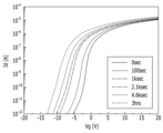
도 7은 도 3에 도시한 종래 기술에 따른 박막 트랜지스터(Qr)의 게이트 전극(124r)에 네거티브 바이어스(negative bias)를 가하는 다양한 시간(0 sec~3hrs)에 따른 박막 트랜지스터(Qr)의 게이트 전압(Vg)-드레인 전류(Id) 특성을 보여주는 그래프이다. 도 7의 그래프에 나타난 바와 같이 박막 트랜지스터(Qr)의 게이트 전극(124r)에 네거티브 바이어스가 가해진 시간에 따라 박막 트랜지스터(Qr)의 특성 변화가 크다.
도 8은 본 발명의 한 실시예에 따른 박막 트랜지스터 패널이 포함하는 박막 트랜지스터(Q)의 게이트 전극(124)에 네거티브 바이어스를 가하는 다양한 시간(0 sec~3hrs)에 따른 박막 트랜지스터(Q)의 게이트 전압(Vg)-드레인 전류(Id) 특성을 보여주는 그래프이다. 도 8을 참조하면, 본 발명의 실시예에 따른 박막 트랜지스터(Q)는 종래 기술에 따른 박막 트랜지스터(Qre)와 비교하여 박막 트랜지스터(Q)의 특성 변화가 작음을 알 수 있다.
또한, 도 3에 도시한 종래 기술에 따른 박막 트랜지스터(Qr)의 경우 게이트 전극(124r)이 반도체 부재(131r)를 기준으로 제1 연결부(173r) 및 제2 연결부(175r)와 같은 쪽에 위치하므로 게이트 전극(124r)과 제1 연결부(173r) 및 제2 연결부(175r)과의 사이에 쇼트(short)가 발생할 위험이 있어 게이트 전극(124r)과 제1 연결부(173r) 및 제2 연결부(175r) 사이에 일정 거리를 두도록 마진을 두고 형성하여야 한다. 즉, 도 3에 도시한 게이트 전극(124r)과 제1 연결부(173r) 또는 제2 연결부(175r) 사이의 평면상 이격 거리(Wr)는 소정의 값 이상을 가지도록 설계되어야 한다. 그러나 본 발명의 실시예에 따르면, 게이트 전극(124)이 반도체 부재(131)를 기준으로 제1 연결부(173) 및 제2 연결부(175)와 반대쪽에 위치하며 채널 영역(134) 위로 다른 도전체가 위치하지 않으므로 제1 연결부(173) 및 제2 연결부(175)와 게이트 전극(124)이나 채널 영역(134) 상의 다른 도전체 사이에 쇼트가 발생할 위험이 적어 게이트 전극(124)과 제1 연결부(173 및 제2 연결부(175) 사이에 평면상 공간 마진을 줄일 수 있다. 즉, 도 1 및 도 2에 도시한 게이트 전극(124)과 제1 연결부(173) 또는 제2 연결부(175) 사이의 평면상 이격 거리(W)를 좁힐 수 있으며, 이격 거리(W)는 0 이상일 수 있다. 이에 따라, 박막 트랜지스터(Q)의 평면상 사이즈를 종래 기술에 비해 줄일 수 있어 고해상도의 박막 트랜지스터 패널을 구현할 수 있다.
또한, 도 3에 도시한 종래 기술에 따른 박막 트랜지스터(Qr)의 경우 게이트 전극(124r)이 반도체 부재(131r)를 기준으로 제1 연결부(173r) 및 제2 연결부(175r)와 같은 쪽에 위치하므로 게이트 전극(124r)과 제1 연결부(173r) 및 제2 연결부(175r)과의 사이에 평면상 기생 용량(Cgs)이 발생하여 앞에서 설명한 기생 용량(Cgs)에 의한 여러 문제점이 동일하게 발생될 수 있다. 그러나 본 발명의 실시예에 따르면, 게이트 전극(124)이 반도체 부재(131)를 기준으로 제1 연결부(173) 및 제2 연결부(175)와 반대쪽에 위치하므로 제1 연결부(173) 및 제2 연결부(175)와 게이트 전극(124)이 평면상 인접하지 않는다. 또한, 채널 영역(134) 상에 제1 및 제2 연결부(173, 175)와 인접하는 다른 도전체가 존재하지 않는다. 따라서 게이트 전극(124)과 제1 연결부(173) 및 제2 연결부(175)과의 사이에 평면상 기생 용량(Cgs)이 발생하지 않아 기생 용량(Cgs)에 의한 여러 문제점이 발생되지 않고 저전력으로 박막 트랜지스터(Q)및 이에 연결된 전기 소자들을 구동할 수 있다.
이와 같이 본 발명의 실시예에 따른 박막 트랜지스터(Q)는 종래 기술에 따른 어떤 구조의 박막 트랜지스터에 비해서도 장점만을 가지고 모든 단점을 해소하여 고해상도, 저전력으로 구동될 수 있는 박막 트랜지스터 패널을 제공할 수 있고, 어떠한 전압 조건 및 시간 조건에서도 향상된 특성을 가지는 박막 트랜지스터가 제공될 수 있다.
그러면, 앞에서 설명한 도면들과 함께 도 9 내지 도 15를 참조하여 본 발명의 한 실시예에 따른 박막 트랜지스터 패널의 제조 방법에 대해 설명한다. 특히, 앞에서 설명한 도 1 및 도 2에 도시한 실시예에 따른 박막 트랜지스터 패널의 제조 방법에 대해 설명하도록 한다.
먼저 도 9를 참조하면, 유리 또는 플라스틱 등의 절연 물질을 포함하는 기판(110) 위에 도전성 물질, 예를 들어 알루미늄(Al), 은(Ag), 구리(Cu), 몰리브덴(Mo), 크롬(Cr), 탄탈륨(Ta), 티타늄(Ti) 등의 금속 또는 이들의 합금 중 적어도 하나를 적층하고 패터닝하여 단일막 또는 다중막 구조의 게이트 전극(124)을 형성한다.
다음 도 10을 참조하면, 게이트 전극(124) 및 기판(110) 위에 산화규소(SiOx), 질화규소(SiNx), 또는 산질화실리콘(SiON) 등의 무기 절연 물질 또는 유기 절연 물질을 적층하여 단일막 또는 다중막 구조의 게이트 절연막(140a)을 형성한다.
이어서, 게이트 절연막(140a) 위에 비정질 규소, 다결정 규소, 산화 아연(ZnO), 아연-주석 산화물(ZTO), 아연-인듐 산화물(ZIO), 인듐 산화물(InO), 티타늄 산화물(TiO), 인듐-갈륨-아연 산화물(IGZO), 인듐-아연-주석 산화물(IZTO)과 같은 산화물 반도체 물질 등을 적층하고 패터닝하여 반도체 부재(130)를 형성한다.
이어서, 반도체 부재(130) 및 게이트 절연막(140a) 위에 산화규소(SiOx), 질화규소(SiNx), 또는 산질화실리콘(SiON) 등의 무기 절연 물질 또는 유기 절연 물질을 적층하여 단일막 또는 다중막 구조의 절연층(140b)을 형성한다. 특히, 반도체 부재(130)가 산화물 반도체를 포함하는 경우, 단일막인 절연층(140b) 또는 다중막인 절연층(140b)의 가장 아래쪽 막은 성막 공정에서 사용되는 가스에 수소(H)가 적게 포함되어 있는 산화규소(SiOx) 등의 무기 절연 물질을 포함할 수 있다.
이어서, 절연층(140b) 위에 배리어층(barrier layer)(150)을 형성한다. 배리어층(150)은 이후에 반도체 부재(130)에 도핑하여 도전 영역을 만들기 위한 수소(H) 등의 불순물이 통과하는 것을 막을 수 있는 금속 등의 물질을 포함할 수 있다. 예를 들어 반도체 부재(130)가 산화물 반도체를 포함하는 경우 배리어층(150)은 티타늄(Ti) 등의 금속 물질 또는 산화물 반도체를 포함할 수 있다.
다음 도 11을 참조하면, 배리어층(150) 위에 포토레지스트 등의 마스크 패턴(50)을 형성하고, 마스크 패턴(50)을 식각 마스크로 하여 배리어층(150) 및 절연층(140b)을 차례대로 식각하여 배리어 패턴(154) 및 배리어 패턴(154) 아래의 배리어막(144)을 형성한다. 이때 배리어 패턴(154) 및 배리어막(144)의 좌우 가장자리는 게이트 전극(124)의 좌우 가장자리와 대체로 정렬되어 있을 수 있거나 게이트 전극(124)과 중첩하는 곳에 위치할 수 있다. 이에 따라 반도체 부재(130)의 일부가 드러난다.
다음 도 12를 참조하면, 마스크 패턴(50)을 없애고, 배리어 패턴(154), 반도체 부재(130) 및 게이트 절연막(140a) 위에 산화규소(SiOx), 질화규소(SiNx), 질산화규소(SiON), 불산화규소(SiOF) 등의 무기 절연 물질 또는 유기 절연 물질을 적층하여 단일막 또는 다중막 구조의 층간 절연막(160)을 형성한다. 특히 반도체 부재(130)가 산화물 반도체를 포함하는 경우 단일막인 층간 절연막(160) 또는 다중막인 층간 절연막(160)의 가장 아래쪽 막은 성막 공정에서 SiH4, NH3 등과 같이 수소를 포함하는 가스를 사용하는 질화규소(SiNx) 등의 질화계 무기 절연 물질을 포함할 수 있다.
층간 절연막(160)의 성막 공정에서 수소(H)를 포함하는 가스의 수소(H) 성분은 배리어 패턴(154)에 의해 덮이지 않은 반도체 부재(130)로 투입 또는 도핑되어 도전성을 가지는 소스 영역(133) 및 드레인 영역(135)이 형성된다. 배리어 패턴(154)으로 덮인 반도체 부재(130)는 배리어 패턴(154)에 의해 수소 또는 불순물이 투입되지 않아 반도체 성질을 유지하는 채널 영역(134)을 이룬다. 이로써, 소스 영역(133), 드레인 영역(135) 및 채널 영역(134)을 포함하는 반도체 부재(131)가 형성된다. 층간 절연막(160)의 성막 후에도 층간 절연막(160)이 포함하는 수소와 같은 불순물이 소스 영역(133) 및 드레인 영역(135)으로 확산될 수 있다.
본 발명의 다른 실시예에 따르면, 층간 절연막(160)을 성막하기 전에, 배리어 패턴(154)에 의해 덮이지 않은 반도체 부재(130)를 환원 처리 또는 n+ 도핑 처리하여 소스 영역(133) 및 드레인 영역(135)을 형성할 수도 있다. 이때 처리 방법으로는 예를 들어 환원 분위기에서의 열처리하는 방법, 수소(H2), 헬륨(He), 포스핀(PH3), 암모니아(NH3), 실란(SiH4), 메탄(CH4), 아세틸렌(C2H2), 디보란(B2H6), 이산화탄소(CO2), 저메인(GeH4), 셀렌화수소(H2Se), 황화수소(H2S), 아르곤(Ar), 질소(N2), 산화 질소(N2O), 플루오르포름(CHF3) 등의 기체 플라즈마를 이용한 플라즈마 처리 방법 등이 있을 수 있다.
다음 도 13을 참조하면, 층간 절연막(160)을 식각 등의 방법으로 패터닝하여 소스 영역(133)을 드러내는 구멍(163), 드레인 영역(135)을 드러내는 구멍(165), 그리고 배리어 패턴(154)을 드러내는 구멍(164)을 형성한다. 구멍(164)은 도 13에 도시한 바와 같이 배리어 패턴(154) 전체를 드러낼 수 있다.
박막 트랜지스터의 종류에 따라 구멍(163)과 구멍(165) 중 적어도 하나는 형성하지 않을 수도 있다.
다음 도 14를 참조하면, 층간 절연막(160) 위에 알루미늄, 은, 구리, 몰리브덴, 크롬, 탄탈륨, 티타늄 등의 금속 또는 이들 금속의 합금 등을 포함하는 도전성 물질을 적층하여 단일막 또는 다중막 구조의 도전층(170)을 형성한다.
다음 도 15를 참조하면, 도전층(170)을 패터닝하여 소스 영역(133)과 연결된 제1 연결부(173), 그리고 드레인 영역(135)과 연결된 제2 연결부(175)를 포함하는 데이터 도전체를 형성한다. 도전층(170)의 패터닝과 함께 배리어 패턴(154)도 식각으로 제거될 수 있다. 이와 달리 도전층(170)의 패터닝 후 배리어 패턴(154)을 식각하여 제거할 수도 있다. 이에 따라 도 15에 도시한 바와 같이 배리어막(144)의 윗면이 드러날 수 있다. 이와 같이 배리어 패턴(154)이 제거되므로 제1 연결부(173) 및 제2 연결부(175)과 쇼트를 발생시킬 수 있는 도전체가 채널 영역(134) 위에서 제거되어 공간 마진을 줄일 수 있어 고해상도의 박막 트랜지스터 패널 및 이를 포함하는 표시 장치를 구현할 수 있다.
다음 앞에서 설명한 도 1 및 도 2를 참조하면, 배리어막(144)과 제1 연결부(173) 및 제2 연결부(175) 위에 무기 절연 물질 및 유기 절연 물질 중 적어도 하나를 적층하여 단일막 또는 다중막 구조의 보호막(180)을 형성한다.
본 발명의 다른 실시예에 따르면, 도 10 내지 도 14에 도시한 바와 달리 배리어층(150) 및 배리어 패턴(154)을 형성하지 않고, 배리어막(144)에 의해서만 반도체 부재(130)가 수소 또는 불순물로 도핑되는 것을 막을 수 있다. 이 경우 배리어막(144)이 수소 또는 불순물의 투과를 차단하기 위해 충분한 두께를 가질 수 있다.
이제, 도 16 및 도 17을 참조하여 본 발명의 한 실시예에 따른 박막 트래지스터 패널에 대하여 설명한다. 앞에서 설명한 실시예와 동일한 구성 요소에 대해서는 동일한 도면 부호를 부여하고, 동일한 설명은 생략하며 차이점을 중심으로 설명한다.
본 발명의 한 실시예에 따른 박막 트래지스터 패널은 박막 트랜지스터(Qa)를 포함한다. 본 실시예에 따른 박막 트랜지스터 패널은 앞에서 설명한 도 1 및 도 2에 도시한 실시예에 따른 박막 트랜지스터 패널과 대부분 동일하나, 반도체 부재(131A), 배리어막(144A) 및 층간 절연막(160)의 구조가 앞에서 설명한 실시예와 다를 수 있다.
반도체 부재(131A)는 게이트 절연막(140a) 위에 위치하며, 채널 영역(134A), 소스 영역(133), 드레인 영역(135), 그리고 버퍼 영역(136)을 포함할 수 있다. 채널 영역(134A), 소스 영역(133) 및 드레인 영역(135)은 앞에서 설명한 실시예의 채널 영역(134), 소스 영역(133) 및 드레인 영역(135)과 동일하므로 이에 대한 상세한 설명은 생략한다.
버퍼 영역(136)은 채널 영역(134A)과 소스 영역(133) 사이, 그리고 채널 영역(134A)과 드레인 영역(135) 사이에 위치하며 저도전 영역(low conductive region)이라고도 한다. 버퍼 영역(136)의 캐리어 농도는 채널 영역(134A)의 캐리어 농도보다 높으나 소스 영역(133) 및 드레인 영역(135)의 캐리어 농도보다 낮다. 버퍼 영역(136)은 소스 영역(133) 및 드레인 영역(135)보다 낮은 도전성을 가질 수 있다. 또한 버퍼 영역(136)의 캐리어 농도는 소스 영역(133) 및 드레인 영역(135)으로부터 채널 영역(134A) 쪽으로 갈수록 점차 감소할 수 있다.
버퍼 영역(136)의 표면에는 반도체 부재(131A)가 포함하는 인듐(In) 등의 금속이 석출되어 있을 수 있다.
반도체 부재(131A) 위에는 배리어막(144A)이 위치한다. 배리어막(144A)은 앞에서 설명한 실시예의 배리어막(144)과 대부분 동일하나, 배리어막(144A)은 채널 영역(134)뿐만 아니라 버퍼 영역(136) 위에 위치하는 외곽부(142)도 포함할 수 있다. 외곽부(142)는 버퍼 영역(136)과 평면상 중첩할 수 있다. 이에 따라 배리어막(144A)의 제1 방향(Dr1) 폭은 채널 영역(134A) 및 양쪽의 버퍼 영역(136)을 포함한 전체의 제1 방향(Dr1) 폭과 실질적으로 동일하거나 약간 클 수 있다. 다르게 설명하면, 채널 영역(134A) 및 양쪽의 버퍼 영역(136)을 포함한 전체의 좌우 가장자리, 즉 버퍼 영역(136)과 소스 영역(133) 사이의 경계 또는 버퍼 영역(136)과 드레인 영역(135) 사이의 경계는 배리어막(144A)의 좌우 가장자리 변과 정렬되어 있거나, 배리어막(144A)과 평면상 중첩할 수 있다.
반도체 부재(131A)의 위에 위치하는 층간 절연막(160)은 앞에서 설명한 실시예의 층간 절연막(160)과 대부분 동일하나, 층간 절연막(160)은 구멍(164)에서 배리어막(144A)의 대부분을 덮고 있지 않을 수 있다. 층간 절연막(160)은 도 17에 도시한 바와 같이 배리어막(144A)의 좌우 가장자리 일부를 덮으며 중첩할 수 있다. 구멍(164)의 제1 방향(Dr1)의 폭은 채널 영역(134A)의 제1 방향(Dr1)의 폭과 같거나 클 수 있으며, 구멍(164)의 평면상 크기는 채널 영역(134A)의 평면상 크기와 같거나 클 수 있다. 구멍(164)의 제1 방향(Dr1)의 폭은 반도체 부재(131A)의 제1 방향(Dr1)의 폭보다 작을 수 있다.
본 실시예에 따르면, 채널 영역(134A)과 소스 영역(133) 또는 드레인 영역(135) 사이의 캐리어 농도를 점차적으로 변화시켜 핫 캐리어의 발생을 억제할 수 있고, 채널 영역(134A)의 채널 길이가 짧아지는 것을 막을 수 있다. 따라서 채널 영역(134A)으로의 전류의 급증을 방지할 수 있다. 또한 박막 트랜지스터(Qa)에 높은 소스-드레인 전압(Vds)이 인가되어도 버퍼 영역(136)에 의해 반도체 부재(131)에 생성되는 전기장 세기를 완화하여 박막 트랜지스터(Qa)의 높은 전압 스트레스에 대한 신뢰성이 더욱 향상되며 더욱 안정된 특성을 나타낼 수 있다.
그러면, 앞에서 설명한 도면들과 함께 도 18 내지 도 22를 참조하여 본 발명의 한 실시예에 따른 박막 트랜지스터 패널의 제조 방법에 대해 설명한다. 특히, 앞에서 설명한 도 16 및 도 17에 도시한 실시예에 따른 박막 트랜지스터 패널의 제조 방법에 대해 설명하도록 한다.
앞에서 설명한 도 9 및 도 10에 도시한 바와 같이, 기판(110) 위에 게이트 전극(124), 게이트 절연막(140a), 반도체 부재(130), 절연층(140b), 그리고 배리어층(150)을 차례대로 형성한다.
다음 도 18을 참조하면, 배리어층(150) 위에 포토레지스트 등의 마스크 패턴(50A)을 형성한다. 마스크 패턴(50A)은 단면상 두께가 상대적으로 두꺼운 제1 부분(51)과 제1 부분(51)보다 얇은 제2 부분(52)을 포함할 수 있다. 제1 부분(51)과 제2 부분(52) 사이의 경계는 게이트 전극(124)의 좌우 가장자리에 대체로 정렬되어 있을 수 있다.
다음 도 19를 참조하면, 마스크 패턴(50A)을 식각 마스크로 하여 배리어층(150) 및 절연층(140b)을 식각하여 배리어 패턴(151) 및 배리어 패턴(151) 아래의 절연층 패턴(141)을 형성한다. 이때 배리어 패턴(151) 및 절연층 패턴(141)의 제1 방향(Dr1)의 폭은 게이트 전극(124)의 제1 방향(Dr1)의 폭보다 클 수 있다.
다음 도 20을 참조하면, 마스크 패턴(50A)을 애싱 등의 방법으로 두께를 줄여 제2 부분(52)을 제거하여 마스크 패턴(51A)을 형성한다. 이에 따라 배리어 패턴(151)의 가장자리 일부가 드러난다.
이어서, 마스크 패턴(51A)을 식각 마스크로 하여 드러난 배리어 패턴(151)의 가장자리를 식각하여 배리어 패턴(154A)을 형성한다. 절연층 패턴(141)은 배리어 패턴(154A)에 의해 덮여 있는 부분 및 배리어 패턴(154A)에 의해 덮이지 않고 드러난 외곽부(142)를 포함하는 배리어막(144A)이 된다.
다음 도 21을 참조하면, 마스크 패턴(51A)을 애싱 등의 방법으로 제거한다.
다음 도 22를 참조하면, 배리어 패턴(154A)에 의해 덮이지 않은 반도체 부재(131A)를 환원 처리 또는 n+ 도핑 처리하여 소스 영역(133) 및 드레인 영역(135), 그리고 버퍼 영역(136)을 형성할 수 있다. 이때 처리 방법으로는 환원 분위기에서의 열처리하는 방법, 수소(H2) 등의 기체 플라즈마를 이용한 플라즈마 처리 방법 등이 있을 수 있다.
배리어 패턴(154A)으로 덮인 반도체 부재(131A)는 채널 영역(134A)을 형성한다. 배리어 패턴(154A)과 중첩하지 않으면서 배리어막(144A)하고만 중첩하는 반도체 부재(131A), 즉 배리어막(144A)의 외곽부(142)와 중첩하는 반도체 부재(131A)의 영역은 소스 영역(133) 및 드레인 영역(135)보다 약하게 처리되어 소스 영역(133) 및 드레인 영역(135)보다 낮은 도전성을 가지며 캐리어 농도가 서서히 변하는 버퍼 영역(136)이 될 수 있다.
반도체 부재(131A)의 환원 처리 시에 반도체 물질의 금속 성분이 소스 영역(133), 드레인 영역(135), 그리고 버퍼 영역(136)의 표면으로 석출될 수 있다.
이어서, 배리어 패턴(154A), 반도체 부재(131A) 및 게이트 절연막(140a) 위에 산화규소(SiOx), 질화규소(SiNx), 질산화규소(SiON), 불산화규소(SiOF) 등의 무기 절연 물질 또는 유기 절연 물질을 적층한다. 이로써 앞에서 설명한 도 16 및 도 17에 도시한 바와 같은 층간 절연막(160)이 형성된다.
층간 절연막(160)의 성막 공정에서 수소(H)를 포함하는 가스의 수소(H) 성분이 배리어 패턴(154A)에 의해 덮이지 않은 반도체 부재(131A)로 투입 또는 도핑되어 도전성을 가지는 소스 영역(133) 및 드레인 영역(135), 그리고 버퍼 영역(136)이 형성될 수도 있다. 이 경우, 앞에서 설명한 층간 절연막(160)의 성막 전 반도체 부재(130)에 대한 처리는 수행하지 않을 수도 있다.
이어서, 층간 절연막(160)을 패터닝하여 소스 영역(133)을 드러내는 구멍(163), 드레인 영역(135)을 드러내는 구멍(165), 그리고 배리어 패턴(154A)을 드러내는 구멍(164)을 형성한 후, 층간 절연막(160) 위에 금속 등의 도전층(도시하지 않음)을 형성하고 도전층을 패터닝하여 소스 영역(133)과 연결된 제1 연결부(173), 그리고 드레인 영역(135)과 연결된 제2 연결부(175)를 포함하는 데이터 도전체를 형성할 수 있다. 이때 도전층의 패터닝과 함께 또는 도전층의 패터닝 후 배리어 패턴(154A)도 제거될 수 있다. 이어서, 배리어막(144A), 제1 연결부(173) 및 제2 연결부(175) 위에 보호막(180)을 형성할 수 있다.
이제, 도 23 및 도 24를 참조하여 본 발명의 한 실시예에 따른 박막 트래지스터 패널에 대하여 설명한다. 앞에서 설명한 실시예와 동일한 구성 요소에 대해서는 동일한 도면 부호를 부여하고, 동일한 설명은 생략하며 차이점을 중심으로 설명한다.
본 발명의 한 실시예에 따른 박막 트래지스터 패널은 박막 트랜지스터(Qb)를 포함한다. 본 실시예에 따른 박막 트랜지스터 패널은 앞에서 설명한 도 1 및 도 2에 도시한 실시예에 따른 박막 트랜지스터 패널과 대부분 동일하나, 채널 영역(134)과 보호막(180) 사이에 앞에서 설명한 실시예의 배리어막(144)이 위치하지 않고, 층간 절연막(160)의 구조가 앞에서 설명한 실시예와 다를 수 있다.
구체적으로, 층간 절연막(160)은 소스 영역(133)과 중첩하는 구멍(163A), 드레인 영역(135)과 중첩하는 구멍(165A), 그리고 채널 영역(134)과 중첩하며 채널 영역(134) 위에 위치하는 구멍(164A)을 포함할 수 있다.
제1 연결부(173) 및 제2 연결부(175)는 각각 구멍(163A, 165A) 안에서 소스 영역(133) 및 드레인 영역(135)과 직접 접촉하며 연결될 수 있고, 반도체 부재(131)의 좌우 가장자리 변을 덮을 수 있다.
구멍(164A)에서 층간 절연막(160)은 채널 영역(134)의 대부분을 덮고 있지 않을 수 있다. 채널 영역(134)은 구멍(164A)과 완전히 중첩할 수 있고, 구멍(164A)의 평면상 크기는 채널 영역(134)의 평면상 크기와 같거나 클 수 있다.
도 24에 도시한 바와 달리 반도체 부재(131) 위에 위치하는 층간 절연막(160)은 모두 제거되어 있을 수도 있다.
보호막(180)은 채널 영역(134)의 윗면과 접촉할 수 있다.
그러면, 앞에서 설명한 도면들과 함께 도 25 내지 도 30을 참조하여 본 발명의 한 실시예에 따른 박막 트랜지스터 패널의 제조 방법에 대해 설명한다.
먼저 기판(110) 위에 게이트 전극(124), 게이트 절연막(140a), 및 반도체 부재(130)를 차례대로 형성한 후, 반도체 부재(130) 및 게이트 절연막(140a) 위에 배리어층(150)을 형성한다. 배리어층(150)은 수소(H) 등의 물질 또는 불순물이 통과하는 것을 막을 수 있는 금속 등의 물질을 포함할 수 있다. 예를 들어 반도체 부재(130)가 산화물 반도체를 포함하는 경우 배리어층(150)은 티타늄(Ti) 등의 금속 물질을 포함할 수 있다.
다음 도 26을 참조하면, 배리어층(150)을 패터닝하여 배리어 패턴(154)을 형성한다. 배리어 패턴(154)의 좌우 가장자리는 게이트 전극(124)의 좌우 가장자리에 대략 정렬되어 있거나 게이트 전극(124)과 평면상 중첩할 수 있다.
다음 27을 참조하면, 배리어 패턴(154), 반도체 부재(130) 및 게이트 절연막(140a) 위에 층간 절연막(160)을 형성한다. 앞에서 설명한 바와 같이 층간 절연막(160)의 성막 공정에서 배리어 패턴(154)에 의해 덮이지 않은 반도체 부재(130)는 도전성을 가지는 소스 영역(133) 및 드레인 영역(135)이 되고 배리어 패턴(154)으로 덮인 반도체 부재(130)는 채널 영역(134)이 되어 반도체 부재(131)가 형성될 수 있다.
본 발명의 다른 실시예에 따르면, 층간 절연막(160)을 성막하기 전에, 배리어 패턴(154)에 의해 덮이지 않은 반도체 부재(130)를 환원 처리 또는 n+ 도핑 처리하여 소스 영역(133) 및 드레인 영역(135)을 형성할 수도 있다.
다음 도 28을 참조하면, 층간 절연막(160)을 패터닝하여 소스 영역(133)을 드러내는 구멍(163A), 드레인 영역(135)을 드러내는 구멍(165A), 그리고 배리어 패턴(154)을 드러내는 구멍(164A)을 형성한다. 구멍(164A)은 배리어 패턴(154) 전체를 드러낼 수 있다. 이와 달리 반도체 부재(131) 위에 위치하는 층간 절연막(160)을 대부분 제거할 수도 있다.
다음 도 29를 참조하면, 층간 절연막(160) 위에 금속 등을 포함하는 도전층(170)을 형성한다. 도전층(170)은 배리어 패턴(154)의 윗면과 접촉할 수 있다.
다음 도 30을 참조하면, 도전층(170)을 패터닝하여 제1 연결부(173) 및 제2 연결부(175)를 포함하는 데이터 도전체를 형성한다. 도전층(170)의 패터닝과 함께 배리어 패턴(154)도 제거되어 채널 영역(134)의 윗면이 드러날 수 있다. 이와 달리 도전층(170)의 패터닝 후 배리어 패턴(154)을 식각하여 제거할 수도 있다.
다음 앞에서 설명한 도 23 및 도 24를 참조하면, 제1 연결부(173) 및 제2 연결부(175) 위에 보호막(180)을 형성한다.
이제, 도 31 및 도 32를 참조하여 본 발명의 한 실시예에 따른 박막 트래지스터 패널의 구조에 대하여 설명한다. 앞에서 설명한 구조와 동일한 구성 요소에 대해서는 동일한 도면 부호를 부여하고, 동일한 설명은 생략하며 차이점을 중심으로 설명한다.
도 31 및 도 32를 참조하면, 본 발명의 한 실시예에 따른 박막 트랜지스터 패널에서 영상을 표시하는 단위인 한 화소(PX)는 기판(110)의 일면 위에 위치하는 구동 트랜지스터(Qd)를 포함하며, 구동 트랜지스터(Qd)는 앞에서 설명한 여러 실시예에 따른 박막 트랜지스터(Q, Qa, Qb)의 구조와 동일할 수 있다. 도 32는 앞에서 설명한 도 1 및 도 2에 도시한 실시예에 따른 박막 트랜지스터(Q)의 구조와 동일한 구동 트랜지스터(Qd)의 단면 구조를 예로서 도시한다.
도 31을 참조하면, 기판(110) 위에 게이트 신호를 전달하는 게이트선(121), 데이터 신호를 전달하는 데이터선(171), 구동 전압을 전달하는 구동 전압선(172), 스위칭 반도체 부재(131s) 및 스위칭 게이트 전극(124s)을 포함하는 스위칭 트랜지스터(Qs), 제3 연결부(173s), 그리고 제4 연결부(175s)가 더 위치할 수 있다.
게이트선(121)은 주로 제1 방향(Dr1)으로 뻗고, 데이터선(171) 및 구동 전압선(172)은 주로 제2 방향(Dr2)으로 뻗을 수 있다.
구동 트랜지스터(Qd)와 연결된 제1 연결부(173)는 구동 전압선(172)과 연결되어 구동 전압을 전달받을 수 있다.
스위칭 반도체 부재(131s)는 스위칭 트랜지스터(Qs)의 채널이 형성되는 채널 영역(134s), 채널 영역(134s)의 양쪽에 각각 위치하는 소스 영역(133s) 및 드레인 영역(135s)을 포함한다. 스위칭 반도체 부재(131s)는 반도체 부재(131)와 동일한 물질을 포함하여 반도체 부재(131)와 동일한 층에 위치할 수도 있고, 다른 종류의 반도체 물질을 포함하여 반도체 부재(131)와 다른 층에 위치할 수도 있다. 예를 들어 스위칭 반도체 부재(131s)는 다결정 규소를 포함하고, 반도체 부재(131)는 산화물 반도체를 포함할 수 있다.
스위칭 게이트 전극(124s)은 게이트 절연막(140a) 또는 다른 절연층(도시하지 않음)을 사이에 두고 채널 영역(134s)과 중첩한다. 스위칭 게이트 전극(124s)은 구동 트랜지스터(Qd)의 게이트 전극(124)과 동일한 층에 위치할 수 있다. 스위칭 게이트 전극(124s)은 게이트선(121)과 연결되어 게이트 신호를 인가받을 수 있다.
층간 절연막(160)은 스위칭 트랜지스터(Qs)의 소스 영역(133s) 위에 위치하는 구멍(163s) 및 드레인 영역(135s) 위에 위치하는 구멍(165s)을 더 포함할 수 있고, 층간 절연막(160) 및 게이트 절연막(140a)은 제4 연결부(175s) 위에 위치하는 구멍(166)을 포함할 수 있다.
제3 연결부(173s) 및 제4 연결부(175s)는 층간 절연막(160) 위에 위치할 수 있다. 제3 연결부(173s)는 구멍(163s)을 통해 소스 영역(133s)과 전기적으로 연결되고, 제4 연결부(175s)는 구멍(165s)을 통해 드레인 영역(135s)과 전기적으로 연결될 수 있다. 제3 연결부(173s)는 데이터선(171)과 연결되어 데이터 신호를 인가받아 스위칭 트랜지스터(Qs)에 전달할 수 있다. 제4 연결부(175s)는 구멍(166)을 통해 구동 트랜지스터(Qd)의 게이트 전극(124)과 전기적으로 연결될 수 있다.
게이트 전극(124)은 도전체(127)와 연결될 수 있다. 도전체(127)는 대부분 층간 절연막(160) 및 게이트 절연막(140a)을 사이에 두고 구동 전압선(172)과 중첩할 수 있다.
보호막(180)은 제2 연결부(175) 위에 위치하며 제2 연결부(175)와 중첩하는 구멍(185)을 포함할 수 있다.
보호막(180) 위에는 화소 전극(191)이 위치할 수 있다. 화소 전극(191)은 구멍(185)을 통해 제2 연결부(175)와 연결되어 전압을 인가받을 수 있다. 보호막(180) 위에는 화소 정의막(350)이 위치할 수 있다. 화소 정의막(350)은 화소 전극(191)의 가장자리의 일부를 덮을 수 있다. 화소 정의막(350)으로 덮이지 않은 화소 전극(191) 위에 발광층(370)이 위치하고, 발광층(370) 위에는 공통 전극(270)이 위치한다. 화소 전극(191), 발광층(370) 및 공통 전극(270)은 함께 유기 발광 다이오드를 형성할 수 있다.
이와 같이, 본 발명의 한 실시예에 따른 박막 트랜지스터 패널을 포함하는 표시 장치는 앞에서 설명한 바와 같이 고해상도를 구현하기 용이하고 저전력으로 구동될 수 있으며 어떤 조건에서도 향상된 특성을 가지는 박막 트랜지스터에 의해 좋은 품질의 영상을 제공할 수 있다.
이상에서 본 발명의 실시예에 대하여 상세하게 설명하였지만 본 발명의 권리범위는 이에 한정되는 것은 아니고 다음의 청구범위에서 정의하고 있는 본 발명의 기본 개념을 이용한 당업자의 여러 변형 및 개량 형태 또한 본 발명의 권리범위에 속하는 것이다.Hereinafter, with reference to the attached drawings, various embodiments of the present invention will be described in detail so that those skilled in the art can easily practice the present invention. The invention may be implemented in many different forms and is not limited to the embodiments described herein.
In order to clearly explain the present invention, parts that are not relevant to the description are omitted, and identical or similar components are given the same reference numerals throughout the specification.
Since the size and thickness of each component shown in the drawings are arbitrarily shown for convenience of explanation, the present invention is not necessarily limited to what is shown. In the drawing, the thickness is enlarged to clearly express various layers and areas. And in the drawings, for convenience of explanation, the thicknesses of some layers and regions are exaggerated.
When a part of a layer, membrane, region, plate, etc. is said to be "on" or "on" another part, this includes not only being "directly above" the other part, but also cases where there is another part in between. Conversely, when a part is said to be “right on top” of another part, it means that there is no other part in between. In addition, being “on” or “on” a reference part means being located above or below the reference part, and does not necessarily mean being located “above” or “on” the direction opposite to gravity. .
Throughout the specification, when it is said that a part “includes” a certain element, this means that it may further include other elements rather than excluding other elements, unless specifically stated to the contrary.
Now, a thin film transistor panel according to an embodiment of the present invention will be described with reference to FIGS. 1 and 2.
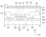
A thin film transistor panel according to an embodiment of the present invention includes a thin film transistor (Q). The thin film transistor Q may be located on one side of the
The first direction Dr1 and the second direction Dr2 shown in FIG. 1 are directions parallel to the main surface of the
The thin film transistor Q includes a
A
The
A
The
The
The left and right edges of the
The
When the
The
A
In a planar structure, the
The
The
An interlayer insulating
Referring to FIG. 2 , the
Unlike shown in FIG. 2, the
The
A data conductor including the
The
The
Depending on the type of thin film transistor Q, at least one of the
A
The
Then, the characteristics of the thin film transistor Q according to this embodiment will be described with reference to the structure of the thin film transistor according to the prior art shown in FIGS. 3 and 4 and the characteristic graphs of the thin film transistor shown in FIGS. 5 to 8. do.
3 and 4 are cross-sectional views of a portion of a thin film transistor panel according to the prior art, respectively.
Referring to FIG. 3, a thin film transistor (Qr) according to the prior art is located on a substrate (111r) and includes a semiconductor member (131r) including a source region (133r), a drain region (135r), and a channel region (134r). , a
Referring to FIG. 4, a thin film transistor (Qre) of another structure according to the prior art includes a gate electrode (124re) located on a substrate (111re), a gate insulating film (140re) located on the gate electrode (124re), and a gate insulating film (140re). ) a semiconductor member 131re positioned on the semiconductor member 131re, an etch stopper 160re positioned on the semiconductor member 131re, a source electrode 173re and a drain electrode 175re positioned on the semiconductor member 131re and the etch stopper 160re, And it may include a protective film 180re located on the source electrode 173re and the drain electrode 175re.
FIG. 5 shows gate voltage (Vg)-drain current (Id) characteristics according to various drain voltages (Vd=0.1V, 10V) before applying stress to the thin film transistor (Qre) according to the prior art shown in FIG. 4 (Initial). and gate voltage (Vg)-drain current (Id) characteristics according to various drain voltages (Vd=0.1V, 10V) after stress. The stress applied to the thin film transistor (Qre) may be, for example, a state in which the source-drain voltage (Vds) is a very high voltage (ex. Vds = 80V, Vgs = 0V). As shown in the graph of FIG. 5, the change in characteristics of the thin film transistor (Qre) is greater after applying stress compared to before applying stress to the thin film transistor (Qre).
FIG. 6 is a graph showing gate voltage (Vg)-drain current (Id) characteristics of a thin film transistor included in a thin film transistor panel according to an embodiment of the present invention. Referring to FIG. 6, the thin film transistor (Q) according to an embodiment of the present invention exhibits the same characteristics as before stress even after being subjected to stress under the same conditions as the thin film transistor (Qre), showing that the characteristics of the thin film transistor (Q) are improved. Able to know.
In the case of the thin film transistor (Qre) according to the prior art shown in FIG. 4, the source electrode 173re and the drain electrode 175re are directly connected to the semiconductor region of the semiconductor member 131re, so a strong electric field is generated near the connection portion. Therefore, especially at a high source-drain voltage (Vds), the semiconductor member 131re becomes vulnerable to stress due to high voltage, thereby reducing the reliability of the thin film transistor (Qre). However, according to this embodiment, like the thin film transistor Qre shown in FIG. 4, the
In addition, in the case of the thin film transistor Qre according to the prior art shown in FIG. 4, the gate electrode 124re overlaps the source electrode 173re and the drain electrode 175re vertically in the cross-sectional structure. Therefore, a significant parasitic capacitance (Cgs) occurs between the gate electrode (124re) and the source electrode (173re) or drain electrode (175re), causing RC delay and kickback voltage to other electrodes (ex. pixel electrode) connected to the thin film transistor (Qre). There are problems such as insufficient voltage being applied and increased power consumption. However, according to an embodiment of the present invention, the
FIG. 7 shows the gate voltage of the thin film transistor (Qr) according to various times (0 sec to 3 hrs) for applying a negative bias to the
Figure 8 shows the gate of the thin film transistor (Q) according to various times (0 sec to 3 hrs) for applying a negative bias to the
In addition, in the case of the thin film transistor Qr according to the prior art shown in FIG. 3, the
In addition, in the case of the thin film transistor Qr according to the prior art shown in FIG. 3, the
In this way, the thin film transistor (Q) according to an embodiment of the present invention has only advantages and overcomes all disadvantages compared to a thin film transistor of any structure according to the prior art, thereby providing a thin film transistor panel that can be driven at high resolution and low power. , a thin film transistor with improved characteristics can be provided under any voltage and time conditions.
Next, a method of manufacturing a thin film transistor panel according to an embodiment of the present invention will be described with reference to FIGS. 9 to 15 along with the drawings described above. In particular, a method of manufacturing a thin film transistor panel according to the embodiment shown in FIGS. 1 and 2 described above will be described.
First, referring to FIG. 9, a conductive material such as aluminum (Al), silver (Ag), copper (Cu), molybdenum (Mo), chromium ( At least one of metals such as Cr), tantalum (Ta), titanium (Ti), or alloys thereof are stacked and patterned to form the
Referring to FIG. 10, an inorganic or organic insulating material such as silicon oxide (SiOx), silicon nitride (SiNx), or silicon oxynitride (SiON) is stacked on the
Subsequently, amorphous silicon, polycrystalline silicon, zinc oxide (ZnO), zinc-tin oxide (ZTO), zinc-indium oxide (ZIO), indium oxide (InO), titanium oxide (TiO), indium- The
Next, an inorganic or organic insulating material such as silicon oxide (SiOx), silicon nitride (SiNx), or silicon oxynitride (SiON) is stacked on the
Next, a
Next, referring to FIG. 11, a
Referring to FIG. 12, the
In the deposition process of the
According to another embodiment of the present invention, before forming the
Next, referring to FIG. 13, the
Depending on the type of thin film transistor, at least one of the
Referring to FIG. 14, a conductive material containing metals such as aluminum, silver, copper, molybdenum, chromium, tantalum, titanium, or alloys of these metals is laminated on the
Next, referring to FIG. 15, the
Next, referring to FIGS. 1 and 2 described above, at least one of an inorganic insulating material and an organic insulating material is laminated on the
According to another embodiment of the present invention, unlike shown in FIGS. 10 to 14, the
Now, a thin film transistor panel according to an embodiment of the present invention will be described with reference to FIGS. 16 and 17. The same reference numerals are assigned to the same components as the previously described embodiments, the same description is omitted, and the description focuses on the differences.
A thin film transistor panel according to an embodiment of the present invention includes a thin film transistor (Qa). The thin film transistor panel according to this embodiment is mostly the same as the thin film transistor panel according to the embodiment shown in FIGS. 1 and 2 described above, but has a structure of the
The
The
A metal such as indium (In) included in the
A
The
According to this embodiment, the generation of hot carriers can be suppressed by gradually changing the carrier concentration between the
Next, a method of manufacturing a thin film transistor panel according to an embodiment of the present invention will be described with reference to FIGS. 18 to 22 along with the drawings described above. In particular, a method of manufacturing a thin film transistor panel according to the embodiment shown in FIGS. 16 and 17 described above will be described.
As shown in FIGS. 9 and 10 described above, a
Next, referring to FIG. 18, a
Next, referring to FIG. 19, the
Next, referring to FIG. 20, the
Next, using the
Next, referring to FIG. 21, the
Next, referring to FIG. 22, the
The
When the
Next, an inorganic insulating material such as silicon oxide (SiOx), silicon nitride (SiNx), silicon nitride (SiON), or silicon fluoroxide (SiOF) or an organic insulating material is applied on the
In the film forming process of the
Subsequently, the
Now, a thin film transistor panel according to an embodiment of the present invention will be described with reference to FIGS. 23 and 24. The same reference numerals are assigned to the same components as the previously described embodiments, the same description is omitted, and the description focuses on the differences.
A thin film transistor panel according to an embodiment of the present invention includes a thin film transistor (Qb). The thin film transistor panel according to this embodiment is mostly the same as the thin film transistor panel according to the embodiment shown in FIGS. 1 and 2 described above, but has a barrier film ( 144) is not located, and the structure of the
Specifically, the
The
In the
Unlike shown in FIG. 24, all of the
The
Next, a method of manufacturing a thin film transistor panel according to an embodiment of the present invention will be described with reference to FIGS. 25 to 30 along with the drawings described above.
First, the
Next, referring to FIG. 26, the
Referring to 27 below, an
According to another embodiment of the present invention, before forming the
Next, referring to FIG. 28, the
Next, referring to FIG. 29, a
Next, referring to FIG. 30, the
Next, referring to FIGS. 23 and 24 described above, a
Now, the structure of a thin film transistor panel according to an embodiment of the present invention will be described with reference to FIGS. 31 and 32. Components that are identical to the structure described above are given the same reference numerals, identical descriptions are omitted, and explanations are focused on differences.
31 and 32, one pixel (PX), which is a unit for displaying an image in a thin film transistor panel according to an embodiment of the present invention, includes a driving transistor (Qd) located on one surface of the
Referring to FIG. 31, on the
The
The
The switching
The switching
The
The
The
The
A
As described above, the display device including the thin film transistor panel according to an embodiment of the present invention is easy to implement high resolution, can be driven at low power, and has good quality due to the thin film transistor with improved characteristics under any conditions. Video can be provided.
Although the embodiments of the present invention have been described in detail above, the scope of the present invention is not limited thereto, and various modifications and improvements made by those skilled in the art using the basic concept of the present invention defined in the following claims are also possible. It falls within the scope of rights.
124: 게이트 전극
131: 반도체 부재
140a: 게이트 절연막
144: 배리어막
160: 층간 절연막
180: 보호막
191: 화소 전극124: Gate electrode
131: Semiconductor member
140a: gate insulating film
144: Barrier
160: Interlayer insulating film
180: Shield
191: Pixel electrode
Claims (20)
상기 기판 위에 위치하는 게이트 전극,
상기 게이트 전극 위에 위치하는 게이트 절연막,
상기 게이트 절연막을 사이에 두고 상기 게이트 전극과 중첩하는 채널 영역, 상기 채널 영역을 사이에 두고 서로 마주하는 소스 영역 및 드레인 영역을 포함하는 반도체 부재,
상기 채널 영역 위에 위치하는 배리어막,
상기 반도체 부재 위에 위치하는 층간 절연막,
상기 층간 절연막 위에 위치하는 데이터 도전체, 그리고
상기 데이터 도전체 위에 위치하는 보호막
을 포함하고,
상기 층간 절연막은 상기 채널 영역 위에 위치하는 제1 구멍, 그리고 상기 소스 영역 또는 상기 드레인 영역 위에 위치하며 상기 제1 구멍과 이격된 제2 구멍을 포함하고,
상기 데이터 도전체는 상기 제2 구멍을 통해 상기 소스 영역 또는 상기 드레인 영역과 접촉하고,
상기 배리어막의 가장자리, 상기 게이트 전극의 가장자리 및 상기 채널 영역의 가장자리는 서로 정렬되어 있고,
상기 보호막은 상기 제1 구멍 안에 위치하는 부분을 포함하는
박막 트랜지스터 패널.Board,
A gate electrode located on the substrate,
A gate insulating film located on the gate electrode,
A semiconductor member including a channel region overlapping the gate electrode with the gate insulating film therebetween, and a source region and a drain region facing each other with the channel region therebetween;
A barrier film located over the channel region,
An interlayer insulating film located on the semiconductor member,
A data conductor located on the interlayer insulating film, and
A protective film located on the data conductor
Including,
The interlayer insulating film includes a first hole located above the channel region, and a second hole located above the source region or the drain region and spaced apart from the first hole,
the data conductor contacts the source region or the drain region through the second hole,
The edge of the barrier film, the edge of the gate electrode, and the edge of the channel region are aligned with each other,
The protective film includes a portion located within the first hole.
Thin film transistor panel.
상기 데이터 도전체와 상기 게이트 전극 사이의 평면상 이격 거리는 0 이상인 박막 트랜지스터 패널.In paragraph 1:
A thin film transistor panel wherein a planar separation distance between the data conductor and the gate electrode is 0 or more.
상기 배리어막의 제1 방향의 폭은 상기 반도체 부재의 제1 방향의 폭보다 작고,
상기 제1 구멍의 상기 제1 방향의 폭은 상기 채널 영역의 상기 제1 방향의 폭 이상인
박막 트랜지스터 패널.In paragraph 3,
The width of the barrier film in the first direction is smaller than the width of the semiconductor member in the first direction,
The width of the first hole in the first direction is greater than or equal to the width of the channel region in the first direction.
Thin film transistor panel.
상기 보호막은 상기 제1 구멍에서 상기 배리어막의 윗면과 접촉하는 박막 트랜지스터 패널.In paragraph 4,
The protective film is in contact with the upper surface of the barrier film through the first hole.
상기 배리어막은 산화규소를 포함하고, 상기 층간 절연막은 질화규소를 포함하는 박막 트랜지스터 패널.In paragraph 5,
A thin film transistor panel wherein the barrier film includes silicon oxide, and the interlayer insulating film includes silicon nitride.
상기 층간 절연막은 질화규소를 포함하는 박막 트랜지스터 패널.In paragraph 3,
A thin film transistor panel wherein the interlayer insulating film includes silicon nitride.
상기 게이트 전극 위에 게이트 절연막을 형성하는 단계,
상기 게이트 절연막 위에 반도체 부재를 형성하는 단계,
상기 반도체 부재 위에 절연층 및 배리어층을 적층하는 단계,
상기 배리어층 및 상기 절연층을 패터닝하여 상기 게이트 전극과 중첩하며 상기 반도체 부재의 적어도 일부를 드러내는 배리어 패턴 및 배리어막을 형성하는 단계,
상기 배리어 패턴 및 상기 드러난 반도체 부재 위에 층간 절연막을 적층하는 단계,
상기 층간 절연막을 패터닝하여 상기 배리어 패턴을 드러내는 제1 구멍, 그리고 상기 반도체 부재 위에 위치하며 상기 제1 구멍과 이격된 제2 구멍을 형성하는 단계,
상기 층간 절연막 위에 도전층을 적층하는 단계,
상기 도전층을 패터닝하여 상기 제2 구멍을 통해 상기 반도체 부재와 접촉하는 데이터 도전체를 형성하는 단계,
상기 배리어 패턴을 제거하는 단계, 그리고
상기 데이터 도전체 위에 보호막을 형성하는 단계
를 포함하고,
상기 배리어막의 가장자리, 상기 게이트 전극의 가장자리 및 상기 반도체 부재의 채널 영역의 가장자리는 서로 정렬되어 있는
박막 트랜지스터 패널의 제조 방법.forming a gate electrode on the substrate,
forming a gate insulating film on the gate electrode,
forming a semiconductor member on the gate insulating film,
Laminating an insulating layer and a barrier layer on the semiconductor member,
Patterning the barrier layer and the insulating layer to form a barrier pattern and a barrier film that overlap the gate electrode and expose at least a portion of the semiconductor member;
Laminating an interlayer insulating film on the barrier pattern and the exposed semiconductor member,
patterning the interlayer insulating film to form a first hole exposing the barrier pattern, and a second hole positioned on the semiconductor member and spaced apart from the first hole;
Laminating a conductive layer on the interlayer insulating film,
patterning the conductive layer to form a data conductor contacting the semiconductor member through the second hole;
removing the barrier pattern, and
Forming a protective film on the data conductor
Including,
The edge of the barrier film, the edge of the gate electrode, and the edge of the channel region of the semiconductor member are aligned with each other.
Manufacturing method of thin film transistor panel.
상기 도전층은 상기 배리어 패턴의 윗면과 접촉하고,
상기 배리어 패턴을 제거하는 단계는 상기 도전층을 패터닝하는 단계와 동시에 또는 상기 도전층을 패터닝한 후 수행되는
박막 트랜지스터 패널의 제조 방법.In paragraph 13:
The conductive layer is in contact with the upper surface of the barrier pattern,
The step of removing the barrier pattern is performed simultaneously with the step of patterning the conductive layer or after patterning the conductive layer.
Manufacturing method of thin film transistor panel.
상기 제1 구멍을 형성하는 단계에서, 상기 제1 구멍은 상기 배리어 패턴 전체를 드러내는 박막 트랜지스터 패널의 제조 방법.In paragraph 14:
In the step of forming the first hole, the first hole exposes the entire barrier pattern.
상기 배리어 패턴의 가장자리는 상기 게이트 전극의 가장자리와 정렬되어 있는 박막 트랜지스터 패널의 제조 방법.In paragraph 15:
A method of manufacturing a thin film transistor panel, wherein the edge of the barrier pattern is aligned with the edge of the gate electrode.
상기 배리어층은 티타늄을 포함하는 금속을 포함하는 박막 트랜지스터 패널의 제조 방법.In paragraph 16:
A method of manufacturing a thin film transistor panel wherein the barrier layer includes a metal including titanium.
상기 보호막은 상기 배리어막의 윗면과 접촉하는 박막 트랜지스터 패널의 제조 방법.In paragraph 13:
A method of manufacturing a thin film transistor panel, wherein the protective film is in contact with the upper surface of the barrier film.
Priority Applications (5)
| Application Number | Priority Date | Filing Date | Title |
|---|---|---|---|
| KR1020160078852A KR102660292B1 (en) | 2016-06-23 | 2016-06-23 | Thin film transistor array panel and manufacturing method thereof |
| US15/436,066 US10217771B2 (en) | 2016-06-23 | 2017-02-17 | Thin film transistor array panel and manufacturing method thereof |
| CN201710337796.3A CN107546231B (en) | 2016-06-23 | 2017-05-15 | Thin Film Transistor Array Panel |
| EP17176847.6A EP3261125B1 (en) | 2016-06-23 | 2017-06-20 | Thin film transistor array panel and manufacturing method thereof |
| US16/241,247 US10396101B2 (en) | 2016-06-23 | 2019-01-07 | Thin film transistor array panel and manufacturing method thereof |
Applications Claiming Priority (1)
| Application Number | Priority Date | Filing Date | Title |
|---|---|---|---|
| KR1020160078852A KR102660292B1 (en) | 2016-06-23 | 2016-06-23 | Thin film transistor array panel and manufacturing method thereof |
Publications (2)
| Publication Number | Publication Date |
|---|---|
| KR20180000792A KR20180000792A (en) | 2018-01-04 |
| KR102660292B1 true KR102660292B1 (en) | 2024-04-24 |
Family
ID=59101306
Family Applications (1)
| Application Number | Title | Priority Date | Filing Date |
|---|---|---|---|
| KR1020160078852A Active KR102660292B1 (en) | 2016-06-23 | 2016-06-23 | Thin film transistor array panel and manufacturing method thereof |
Country Status (4)
| Country | Link |
|---|---|
| US (2) | US10217771B2 (en) |
| EP (1) | EP3261125B1 (en) |
| KR (1) | KR102660292B1 (en) |
| CN (1) | CN107546231B (en) |
Families Citing this family (9)
| Publication number | Priority date | Publication date | Assignee | Title |
|---|---|---|---|---|
| KR102660292B1 (en) | 2016-06-23 | 2024-04-24 | 삼성디스플레이 주식회사 | Thin film transistor array panel and manufacturing method thereof |
| CN106229297B (en) * | 2016-09-18 | 2019-04-02 | 深圳市华星光电技术有限公司 | The production method of AMOLED pixel-driving circuit |
| CN106981520B (en) * | 2017-04-12 | 2020-07-07 | 京东方科技集团股份有限公司 | Thin film transistor, preparation method thereof, array substrate and display device |
| US20190019472A1 (en) * | 2017-07-13 | 2019-01-17 | Vanguard International Semiconductor Corporation | Display system and method for forming an output buffer of a source driver |
| CN107819039A (en) * | 2017-11-09 | 2018-03-20 | 深圳市华星光电半导体显示技术有限公司 | Thin film transistor (TFT), method for fabricating thin film transistor and liquid crystal display device |
| CN109037075B (en) * | 2018-08-09 | 2023-01-13 | 京东方科技集团股份有限公司 | Manufacturing method of thin film transistor, transistor and display substrate |
| CN112530978B (en) * | 2020-12-01 | 2024-02-13 | 京东方科技集团股份有限公司 | Switching device structure and preparation method thereof, thin film transistor film layer, display panel |
| CN113314615A (en) * | 2021-06-04 | 2021-08-27 | 华南理工大学 | Thin film transistor and preparation method thereof |
| CN114171603B (en) * | 2021-12-08 | 2025-04-25 | 深圳市华星光电半导体显示技术有限公司 | Driving substrate and manufacturing method thereof, and display panel |
Citations (5)
| Publication number | Priority date | Publication date | Assignee | Title |
|---|---|---|---|---|
| JP2005072144A (en) | 2003-08-21 | 2005-03-17 | Seiko Epson Corp | Thin film semiconductor device and manufacturing method thereof, electro-optical device, and electronic apparatus |
| JP2005079283A (en) * | 2003-08-29 | 2005-03-24 | Seiko Epson Corp | Thin film semiconductor device and manufacturing method thereof, electro-optical device, and electronic apparatus |
| JP2008227157A (en) * | 2007-03-13 | 2008-09-25 | Seiko Epson Corp | Semiconductor device and manufacturing method thereof, active matrix substrate, electro-optical device, and electronic apparatus |
| CN103383945A (en) * | 2013-07-03 | 2013-11-06 | 北京京东方光电科技有限公司 | Array substrate, display device and manufacturing method of array substrate |
| JP2015144250A (en) | 2013-12-27 | 2015-08-06 | 株式会社半導体エネルギー研究所 | semiconductor device |
Family Cites Families (34)
| Publication number | Priority date | Publication date | Assignee | Title |
|---|---|---|---|---|
| US5427962A (en) * | 1991-11-15 | 1995-06-27 | Casio Computer Co., Ltd. | Method of making a thin film transistor |
| US6900854B1 (en) * | 1998-11-26 | 2005-05-31 | Samsung Electronics Co., Ltd. | Thin film transistor array panel for a liquid crystal display |
| KR100770470B1 (en) | 2000-06-30 | 2007-10-26 | 비오이 하이디스 테크놀로지 주식회사 | Method for forming gate electrode of liquid crystal display element |
| KR100720087B1 (en) * | 2000-07-31 | 2007-05-18 | 삼성전자주식회사 | Display element wiring, thin film transistor substrate using same, and manufacturing method thereof |
| TW462135B (en) * | 2000-08-04 | 2001-11-01 | Acer Display Tech Inc | Method for manufacturing the electronic device of thin film transistor display |
| TWI220029B (en) * | 2000-10-12 | 2004-08-01 | Au Optronics Corp | Thin film transistor liquid crystal display and its manufacturing method |
| US6939754B2 (en) | 2003-08-13 | 2005-09-06 | Sharp Laboratories Of America, Inc. | Isotropic polycrystalline silicon and method for producing same |
| TWI221341B (en) * | 2003-09-18 | 2004-09-21 | Ind Tech Res Inst | Method and material for forming active layer of thin film transistor |
| KR101188868B1 (en) * | 2005-06-30 | 2012-10-09 | 삼성디스플레이 주식회사 | Thin film transistor plate and method of fabricating the same |
| KR20070013132A (en) * | 2005-07-25 | 2007-01-30 | 삼성전자주식회사 | Method of manufacturing thin film transistor substrate and thin film transistor substrate |
| JP2007109876A (en) * | 2005-10-13 | 2007-04-26 | Toshiba Matsushita Display Technology Co Ltd | Thin film transistor and manufacturing method thereof |
| KR100817215B1 (en) | 2006-11-30 | 2008-03-27 | 한국전자통신연구원 | Self-aligned organic field effect transistor and its manufacturing method |
| KR100787464B1 (en) * | 2007-01-08 | 2007-12-26 | 삼성에스디아이 주식회사 | Thin film transistor, and manufacturing method thereof |
| KR100832873B1 (en) | 2007-07-02 | 2008-06-02 | 한국기계연구원 | Self-aligned organic thin film transistor and its manufacturing method |
| KR100963104B1 (en) * | 2008-07-08 | 2010-06-14 | 삼성모바일디스플레이주식회사 | Thin film transistor, its manufacturing method, and flat panel display device comprising thin film transistor |
| KR101140135B1 (en) * | 2008-12-05 | 2012-05-02 | 한국전자통신연구원 | Fabrication method of thin film transistor and thin film transistor substrate |
| US20120043543A1 (en) * | 2009-04-17 | 2012-02-23 | Sharp Kabushiki Kaisha | Semiconductor device and manufacturing method therefor |
| TW201214573A (en) | 2010-09-21 | 2012-04-01 | Ying-Jia Xue | Method of fabricating a thin film transistor substrate |
| KR101372852B1 (en) | 2010-10-05 | 2014-03-10 | 삼성디스플레이 주식회사 | Organic light emitting display device and manufacturing method of the same |
| KR20130136063A (en) | 2012-06-04 | 2013-12-12 | 삼성디스플레이 주식회사 | Thin film transistor, thin film transistor array panel including the same and manufacturing method thereof |
| KR101434366B1 (en) * | 2012-08-24 | 2014-08-26 | 삼성디스플레이 주식회사 | Thin-film transistor array substrate, display apparatus comprising the same |
| KR20140087693A (en) * | 2012-12-31 | 2014-07-09 | 삼성디스플레이 주식회사 | Thin film transistor, thin film transistor array panel including the same and manufacturing method thereof |
| JP2014192420A (en) | 2013-03-28 | 2014-10-06 | Japan Display Inc | Semiconductor device, method of manufacturing the same, and display device using the same |
| KR102091663B1 (en) * | 2013-06-28 | 2020-03-23 | 삼성디스플레이 주식회사 | Thin film transistor and organic light emitting diode display |
| KR20150011219A (en) * | 2013-07-22 | 2015-01-30 | 삼성디스플레이 주식회사 | Thin film transistor and thin film transistor array panel including the same |
| KR102148957B1 (en) * | 2013-09-02 | 2020-08-31 | 삼성디스플레이 주식회사 | Display substrate and method of manufacturing a display substrate |
| KR102040011B1 (en) | 2013-12-26 | 2019-11-05 | 엘지디스플레이 주식회사 | Electrostatic discharging device of display device and method of manufacturing the same |
| KR102166898B1 (en) * | 2014-01-10 | 2020-10-19 | 삼성디스플레이 주식회사 | Thin film transistor array panel and method for manufacturing the same |
| TWI535034B (en) | 2014-01-29 | 2016-05-21 | 友達光電股份有限公司 | Pixel structure and its making method |
| KR102172972B1 (en) * | 2014-02-26 | 2020-11-03 | 삼성디스플레이 주식회사 | Thin film transistor and method for fabricating the same |
| KR20160106848A (en) * | 2015-03-02 | 2016-09-13 | 삼성디스플레이 주식회사 | Organic light emitting diode display and method of manufacturng the same |
| CN104882485A (en) | 2015-03-30 | 2015-09-02 | 深超光电(深圳)有限公司 | Thin film transistor and manufacturing method thereof |
| KR102397799B1 (en) * | 2015-06-30 | 2022-05-16 | 엘지디스플레이 주식회사 | Thin Film Transistor And Display Device Comprising The Same |
| KR102660292B1 (en) | 2016-06-23 | 2024-04-24 | 삼성디스플레이 주식회사 | Thin film transistor array panel and manufacturing method thereof |
-
2016
- 2016-06-23 KR KR1020160078852A patent/KR102660292B1/en active Active
-
2017
- 2017-02-17 US US15/436,066 patent/US10217771B2/en active Active
- 2017-05-15 CN CN201710337796.3A patent/CN107546231B/en active Active
- 2017-06-20 EP EP17176847.6A patent/EP3261125B1/en active Active
-
2019
- 2019-01-07 US US16/241,247 patent/US10396101B2/en active Active
Patent Citations (5)
| Publication number | Priority date | Publication date | Assignee | Title |
|---|---|---|---|---|
| JP2005072144A (en) | 2003-08-21 | 2005-03-17 | Seiko Epson Corp | Thin film semiconductor device and manufacturing method thereof, electro-optical device, and electronic apparatus |
| JP2005079283A (en) * | 2003-08-29 | 2005-03-24 | Seiko Epson Corp | Thin film semiconductor device and manufacturing method thereof, electro-optical device, and electronic apparatus |
| JP2008227157A (en) * | 2007-03-13 | 2008-09-25 | Seiko Epson Corp | Semiconductor device and manufacturing method thereof, active matrix substrate, electro-optical device, and electronic apparatus |
| CN103383945A (en) * | 2013-07-03 | 2013-11-06 | 北京京东方光电科技有限公司 | Array substrate, display device and manufacturing method of array substrate |
| JP2015144250A (en) | 2013-12-27 | 2015-08-06 | 株式会社半導体エネルギー研究所 | semiconductor device |
Also Published As
| Publication number | Publication date |
|---|---|
| CN107546231B (en) | 2023-08-04 |
| US10217771B2 (en) | 2019-02-26 |
| EP3261125B1 (en) | 2025-03-26 |
| US10396101B2 (en) | 2019-08-27 |
| US20170373091A1 (en) | 2017-12-28 |
| US20190139992A1 (en) | 2019-05-09 |
| KR20180000792A (en) | 2018-01-04 |
| EP3261125A1 (en) | 2017-12-27 |
| CN107546231A (en) | 2018-01-05 |
Similar Documents
| Publication | Publication Date | Title |
|---|---|---|
| KR102660292B1 (en) | Thin film transistor array panel and manufacturing method thereof | |
| KR102488959B1 (en) | Thin film transistor array panel and manufacturing method thereof | |
| US9343583B2 (en) | Thin film transistor and thin film transistor array panel including the same | |
| US9379252B2 (en) | Thin film transistor and thin film transistor array panel including the same | |
| KR102650692B1 (en) | Thin film transistor, thin film transistor array panel including the same and manufacturing method thereof | |
| KR102867885B1 (en) | Thin film transistor, thin film transistor array panel including the same and manufacturing method thereof | |
| KR102402599B1 (en) | Transistor array panel and manufacturing method thereof | |
| KR20170124152A (en) | Transistor panel and manufacturing method thereof | |
| KR102923319B1 (en) | Thin film transistor, thin film transistor array panel including the same and manufacturing method thereof | |
| KR102130548B1 (en) | Thin film transistor, thin film transistor array panel including the same and manufacturing method thereof |
Legal Events
| Date | Code | Title | Description |
|---|---|---|---|
| PA0109 | Patent application |
St.27 status event code: A-0-1-A10-A12-nap-PA0109 |
|
| PG1501 | Laying open of application |
St.27 status event code: A-1-1-Q10-Q12-nap-PG1501 |
|
| R18-X000 | Changes to party contact information recorded |
St.27 status event code: A-3-3-R10-R18-oth-X000 |
|
| PA0201 | Request for examination |
St.27 status event code: A-1-2-D10-D11-exm-PA0201 |
|
| E902 | Notification of reason for refusal | ||
| PE0902 | Notice of grounds for rejection |
St.27 status event code: A-1-2-D10-D21-exm-PE0902 |
|
| P22-X000 | Classification modified |
St.27 status event code: A-2-2-P10-P22-nap-X000 |
|
| P22-X000 | Classification modified |
St.27 status event code: A-2-2-P10-P22-nap-X000 |
|
| E13-X000 | Pre-grant limitation requested |
St.27 status event code: A-2-3-E10-E13-lim-X000 |
|
| P11-X000 | Amendment of application requested |
St.27 status event code: A-2-2-P10-P11-nap-X000 |
|
| P13-X000 | Application amended |
St.27 status event code: A-2-2-P10-P13-nap-X000 |
|
| E90F | Notification of reason for final refusal | ||
| PE0902 | Notice of grounds for rejection |
St.27 status event code: A-1-2-D10-D21-exm-PE0902 |
|
| E13-X000 | Pre-grant limitation requested |
St.27 status event code: A-2-3-E10-E13-lim-X000 |
|
| P11-X000 | Amendment of application requested |
St.27 status event code: A-2-2-P10-P11-nap-X000 |
|
| P13-X000 | Application amended |
St.27 status event code: A-2-2-P10-P13-nap-X000 |
|
| E701 | Decision to grant or registration of patent right | ||
| PE0701 | Decision of registration |
St.27 status event code: A-1-2-D10-D22-exm-PE0701 |
|
| GRNT | Written decision to grant | ||
| PR0701 | Registration of establishment |
St.27 status event code: A-2-4-F10-F11-exm-PR0701 |
|
| PR1002 | Payment of registration fee |
St.27 status event code: A-2-2-U10-U11-oth-PR1002 Fee payment year number: 1 |
|
| PG1601 | Publication of registration |
St.27 status event code: A-4-4-Q10-Q13-nap-PG1601 |
|
| P22-X000 | Classification modified |
St.27 status event code: A-4-4-P10-P22-nap-X000 |
|
| P22-X000 | Classification modified |
St.27 status event code: A-4-4-P10-P22-nap-X000 |