KR102579784B1 - Selective deposition of thin film dielectrics using surface blocking chemistry - Google Patents
Selective deposition of thin film dielectrics using surface blocking chemistry Download PDFInfo
- Publication number
- KR102579784B1 KR102579784B1 KR1020160053287A KR20160053287A KR102579784B1 KR 102579784 B1 KR102579784 B1 KR 102579784B1 KR 1020160053287 A KR1020160053287 A KR 1020160053287A KR 20160053287 A KR20160053287 A KR 20160053287A KR 102579784 B1 KR102579784 B1 KR 102579784B1
- Authority
- KR
- South Korea
- Prior art keywords
- substrate
- silylamide
- film
- terminated
- terminated surface
- Prior art date
- Legal status (The legal status is an assumption and is not a legal conclusion. Google has not performed a legal analysis and makes no representation as to the accuracy of the status listed.)
- Active
Links
Images

Classifications
-
- H10W20/041—
-
- H—ELECTRICITY
- H01—ELECTRIC ELEMENTS
- H01L—SEMICONDUCTOR DEVICES NOT COVERED BY CLASS H10
- H01L21/00—Processes or apparatus adapted for the manufacture or treatment of semiconductor or solid state devices or of parts thereof
- H01L21/70—Manufacture or treatment of devices consisting of a plurality of solid state components formed in or on a common substrate or of parts thereof; Manufacture of integrated circuit devices or of parts thereof
- H01L21/71—Manufacture of specific parts of devices defined in group H01L21/70
- H01L21/768—Applying interconnections to be used for carrying current between separate components within a device comprising conductors and dielectrics
- H01L21/76838—Applying interconnections to be used for carrying current between separate components within a device comprising conductors and dielectrics characterised by the formation and the after-treatment of the conductors
- H01L21/76841—Barrier, adhesion or liner layers
- H01L21/76868—Forming or treating discontinuous thin films, e.g. repair, enhancement or reinforcement of discontinuous thin films
-
- C—CHEMISTRY; METALLURGY
- C23—COATING METALLIC MATERIAL; COATING MATERIAL WITH METALLIC MATERIAL; CHEMICAL SURFACE TREATMENT; DIFFUSION TREATMENT OF METALLIC MATERIAL; COATING BY VACUUM EVAPORATION, BY SPUTTERING, BY ION IMPLANTATION OR BY CHEMICAL VAPOUR DEPOSITION, IN GENERAL; INHIBITING CORROSION OF METALLIC MATERIAL OR INCRUSTATION IN GENERAL
- C23C—COATING METALLIC MATERIAL; COATING MATERIAL WITH METALLIC MATERIAL; SURFACE TREATMENT OF METALLIC MATERIAL BY DIFFUSION INTO THE SURFACE, BY CHEMICAL CONVERSION OR SUBSTITUTION; COATING BY VACUUM EVAPORATION, BY SPUTTERING, BY ION IMPLANTATION OR BY CHEMICAL VAPOUR DEPOSITION, IN GENERAL
- C23C16/00—Chemical coating by decomposition of gaseous compounds, without leaving reaction products of surface material in the coating, i.e. chemical vapour deposition [CVD] processes
- C23C16/04—Coating on selected surface areas, e.g. using masks
-
- H—ELECTRICITY
- H05—ELECTRIC TECHNIQUES NOT OTHERWISE PROVIDED FOR
- H05K—PRINTED CIRCUITS; CASINGS OR CONSTRUCTIONAL DETAILS OF ELECTRIC APPARATUS; MANUFACTURE OF ASSEMBLAGES OF ELECTRICAL COMPONENTS
- H05K1/00—Printed circuits
- H05K1/02—Details
- H05K1/0296—Conductive pattern lay-out details not covered by sub groups H05K1/02 - H05K1/0295
-
- C—CHEMISTRY; METALLURGY
- C07—ORGANIC CHEMISTRY
- C07F—ACYCLIC, CARBOCYCLIC OR HETEROCYCLIC COMPOUNDS CONTAINING ELEMENTS OTHER THAN CARBON, HYDROGEN, HALOGEN, OXYGEN, NITROGEN, SULFUR, SELENIUM OR TELLURIUM
- C07F7/00—Compounds containing elements of Groups 4 or 14 of the Periodic Table
-
- C—CHEMISTRY; METALLURGY
- C23—COATING METALLIC MATERIAL; COATING MATERIAL WITH METALLIC MATERIAL; CHEMICAL SURFACE TREATMENT; DIFFUSION TREATMENT OF METALLIC MATERIAL; COATING BY VACUUM EVAPORATION, BY SPUTTERING, BY ION IMPLANTATION OR BY CHEMICAL VAPOUR DEPOSITION, IN GENERAL; INHIBITING CORROSION OF METALLIC MATERIAL OR INCRUSTATION IN GENERAL
- C23C—COATING METALLIC MATERIAL; COATING MATERIAL WITH METALLIC MATERIAL; SURFACE TREATMENT OF METALLIC MATERIAL BY DIFFUSION INTO THE SURFACE, BY CHEMICAL CONVERSION OR SUBSTITUTION; COATING BY VACUUM EVAPORATION, BY SPUTTERING, BY ION IMPLANTATION OR BY CHEMICAL VAPOUR DEPOSITION, IN GENERAL
- C23C16/00—Chemical coating by decomposition of gaseous compounds, without leaving reaction products of surface material in the coating, i.e. chemical vapour deposition [CVD] processes
- C23C16/44—Chemical coating by decomposition of gaseous compounds, without leaving reaction products of surface material in the coating, i.e. chemical vapour deposition [CVD] processes characterised by the method of coating
- C23C16/455—Chemical coating by decomposition of gaseous compounds, without leaving reaction products of surface material in the coating, i.e. chemical vapour deposition [CVD] processes characterised by the method of coating characterised by the method used for introducing gases into reaction chamber or for modifying gas flows in reaction chamber
- C23C16/45523—Pulsed gas flow or change of composition over time
- C23C16/45525—Atomic layer deposition [ALD]
-
- C—CHEMISTRY; METALLURGY
- C23—COATING METALLIC MATERIAL; COATING MATERIAL WITH METALLIC MATERIAL; CHEMICAL SURFACE TREATMENT; DIFFUSION TREATMENT OF METALLIC MATERIAL; COATING BY VACUUM EVAPORATION, BY SPUTTERING, BY ION IMPLANTATION OR BY CHEMICAL VAPOUR DEPOSITION, IN GENERAL; INHIBITING CORROSION OF METALLIC MATERIAL OR INCRUSTATION IN GENERAL
- C23C—COATING METALLIC MATERIAL; COATING MATERIAL WITH METALLIC MATERIAL; SURFACE TREATMENT OF METALLIC MATERIAL BY DIFFUSION INTO THE SURFACE, BY CHEMICAL CONVERSION OR SUBSTITUTION; COATING BY VACUUM EVAPORATION, BY SPUTTERING, BY ION IMPLANTATION OR BY CHEMICAL VAPOUR DEPOSITION, IN GENERAL
- C23C16/00—Chemical coating by decomposition of gaseous compounds, without leaving reaction products of surface material in the coating, i.e. chemical vapour deposition [CVD] processes
- C23C16/44—Chemical coating by decomposition of gaseous compounds, without leaving reaction products of surface material in the coating, i.e. chemical vapour deposition [CVD] processes characterised by the method of coating
- C23C16/50—Chemical coating by decomposition of gaseous compounds, without leaving reaction products of surface material in the coating, i.e. chemical vapour deposition [CVD] processes characterised by the method of coating using electric discharges
-
- G—PHYSICS
- G03—PHOTOGRAPHY; CINEMATOGRAPHY; ANALOGOUS TECHNIQUES USING WAVES OTHER THAN OPTICAL WAVES; ELECTROGRAPHY; HOLOGRAPHY
- G03G—ELECTROGRAPHY; ELECTROPHOTOGRAPHY; MAGNETOGRAPHY
- G03G15/00—Apparatus for electrographic processes using a charge pattern
- G03G15/50—Machine control of apparatus for electrographic processes using a charge pattern, e.g. regulating differents parts of the machine, multimode copiers, microprocessor control
-
- G—PHYSICS
- G03—PHOTOGRAPHY; CINEMATOGRAPHY; ANALOGOUS TECHNIQUES USING WAVES OTHER THAN OPTICAL WAVES; ELECTROGRAPHY; HOLOGRAPHY
- G03G—ELECTROGRAPHY; ELECTROPHOTOGRAPHY; MAGNETOGRAPHY
- G03G15/00—Apparatus for electrographic processes using a charge pattern
- G03G15/80—Details relating to power supplies, circuits boards, electrical connections
-
- G—PHYSICS
- G03—PHOTOGRAPHY; CINEMATOGRAPHY; ANALOGOUS TECHNIQUES USING WAVES OTHER THAN OPTICAL WAVES; ELECTROGRAPHY; HOLOGRAPHY
- G03G—ELECTROGRAPHY; ELECTROPHOTOGRAPHY; MAGNETOGRAPHY
- G03G21/00—Arrangements not provided for by groups G03G13/00 - G03G19/00, e.g. cleaning, elimination of residual charge
- G03G21/16—Mechanical means for facilitating the maintenance of the apparatus, e.g. modular arrangements
- G03G21/1642—Mechanical means for facilitating the maintenance of the apparatus, e.g. modular arrangements for connecting the different parts of the apparatus
- G03G21/1652—Electrical connection means
-
- H—ELECTRICITY
- H01—ELECTRIC ELEMENTS
- H01L—SEMICONDUCTOR DEVICES NOT COVERED BY CLASS H10
- H01L21/00—Processes or apparatus adapted for the manufacture or treatment of semiconductor or solid state devices or of parts thereof
- H01L21/02—Manufacture or treatment of semiconductor devices or of parts thereof
- H01L21/02104—Forming layers
- H01L21/02107—Forming insulating materials on a substrate
- H01L21/02225—Forming insulating materials on a substrate characterised by the process for the formation of the insulating layer
- H01L21/0226—Forming insulating materials on a substrate characterised by the process for the formation of the insulating layer formation by a deposition process
- H01L21/02263—Forming insulating materials on a substrate characterised by the process for the formation of the insulating layer formation by a deposition process deposition from the gas or vapour phase
-
- H—ELECTRICITY
- H01—ELECTRIC ELEMENTS
- H01L—SEMICONDUCTOR DEVICES NOT COVERED BY CLASS H10
- H01L21/00—Processes or apparatus adapted for the manufacture or treatment of semiconductor or solid state devices or of parts thereof
- H01L21/70—Manufacture or treatment of devices consisting of a plurality of solid state components formed in or on a common substrate or of parts thereof; Manufacture of integrated circuit devices or of parts thereof
- H01L21/702—Manufacture or treatment of devices consisting of a plurality of solid state components formed in or on a common substrate or of parts thereof; Manufacture of integrated circuit devices or of parts thereof of thick-or thin-film circuits or parts thereof
- H01L21/707—Manufacture or treatment of devices consisting of a plurality of solid state components formed in or on a common substrate or of parts thereof; Manufacture of integrated circuit devices or of parts thereof of thick-or thin-film circuits or parts thereof of thin-film circuits or parts thereof
-
- H—ELECTRICITY
- H01—ELECTRIC ELEMENTS
- H01L—SEMICONDUCTOR DEVICES NOT COVERED BY CLASS H10
- H01L21/00—Processes or apparatus adapted for the manufacture or treatment of semiconductor or solid state devices or of parts thereof
- H01L21/70—Manufacture or treatment of devices consisting of a plurality of solid state components formed in or on a common substrate or of parts thereof; Manufacture of integrated circuit devices or of parts thereof
- H01L21/71—Manufacture of specific parts of devices defined in group H01L21/70
- H01L21/768—Applying interconnections to be used for carrying current between separate components within a device comprising conductors and dielectrics
- H01L21/76801—Applying interconnections to be used for carrying current between separate components within a device comprising conductors and dielectrics characterised by the formation and the after-treatment of the dielectrics, e.g. smoothing
- H01L21/76829—Applying interconnections to be used for carrying current between separate components within a device comprising conductors and dielectrics characterised by the formation and the after-treatment of the dielectrics, e.g. smoothing characterised by the formation of thin functional dielectric layers, e.g. dielectric etch-stop, barrier, capping or liner layers
-
- H—ELECTRICITY
- H05—ELECTRIC TECHNIQUES NOT OTHERWISE PROVIDED FOR
- H05K—PRINTED CIRCUITS; CASINGS OR CONSTRUCTIONAL DETAILS OF ELECTRIC APPARATUS; MANUFACTURE OF ASSEMBLAGES OF ELECTRICAL COMPONENTS
- H05K1/00—Printed circuits
- H05K1/02—Details
- H05K1/0266—Marks, test patterns or identification means
- H05K1/0269—Marks, test patterns or identification means for visual or optical inspection
-
- H—ELECTRICITY
- H05—ELECTRIC TECHNIQUES NOT OTHERWISE PROVIDED FOR
- H05K—PRINTED CIRCUITS; CASINGS OR CONSTRUCTIONAL DETAILS OF ELECTRIC APPARATUS; MANUFACTURE OF ASSEMBLAGES OF ELECTRICAL COMPONENTS
- H05K1/00—Printed circuits
- H05K1/02—Details
- H05K1/11—Printed elements for providing electric connections to or between printed circuits
- H05K1/117—Pads along the edge of rigid circuit boards, e.g. for pluggable connectors
-
- H—ELECTRICITY
- H05—ELECTRIC TECHNIQUES NOT OTHERWISE PROVIDED FOR
- H05K—PRINTED CIRCUITS; CASINGS OR CONSTRUCTIONAL DETAILS OF ELECTRIC APPARATUS; MANUFACTURE OF ASSEMBLAGES OF ELECTRICAL COMPONENTS
- H05K3/00—Apparatus or processes for manufacturing printed circuits
- H05K3/40—Forming printed elements for providing electric connections to or between printed circuits
- H05K3/403—Edge contacts; Windows or holes in the substrate having plural connections on the walls thereof
-
- H—ELECTRICITY
- H10—SEMICONDUCTOR DEVICES; ELECTRIC SOLID-STATE DEVICES NOT OTHERWISE PROVIDED FOR
- H10D—INORGANIC ELECTRIC SEMICONDUCTOR DEVICES
- H10D84/00—Integrated devices formed in or on semiconductor substrates that comprise only semiconducting layers, e.g. on Si wafers or on GaAs-on-Si wafers
- H10D84/01—Manufacture or treatment
-
- H10P10/128—
-
- H10P14/61—
-
- H10P14/6328—
-
- H10P14/6339—
-
- H10P14/6508—
-
- H10P14/6682—
-
- H10P14/69433—
-
- H10P50/242—
-
- H10P50/287—
-
- H10P72/0468—
-
- H10P95/00—
-
- H10W20/071—
-
- H10W20/074—
-
- H—ELECTRICITY
- H05—ELECTRIC TECHNIQUES NOT OTHERWISE PROVIDED FOR
- H05K—PRINTED CIRCUITS; CASINGS OR CONSTRUCTIONAL DETAILS OF ELECTRIC APPARATUS; MANUFACTURE OF ASSEMBLAGES OF ELECTRICAL COMPONENTS
- H05K2201/00—Indexing scheme relating to printed circuits covered by H05K1/00
- H05K2201/03—Conductive materials
- H05K2201/0332—Structure of the conductor
- H05K2201/0388—Other aspects of conductors
- H05K2201/0394—Conductor crossing over a hole in the substrate or a gap between two separate substrate parts
-
- H—ELECTRICITY
- H05—ELECTRIC TECHNIQUES NOT OTHERWISE PROVIDED FOR
- H05K—PRINTED CIRCUITS; CASINGS OR CONSTRUCTIONAL DETAILS OF ELECTRIC APPARATUS; MANUFACTURE OF ASSEMBLAGES OF ELECTRICAL COMPONENTS
- H05K2201/00—Indexing scheme relating to printed circuits covered by H05K1/00
- H05K2201/09—Shape and layout
- H05K2201/09009—Substrate related
- H05K2201/09063—Holes or slots in insulating substrate not used for electrical connections
-
- H—ELECTRICITY
- H05—ELECTRIC TECHNIQUES NOT OTHERWISE PROVIDED FOR
- H05K—PRINTED CIRCUITS; CASINGS OR CONSTRUCTIONAL DETAILS OF ELECTRIC APPARATUS; MANUFACTURE OF ASSEMBLAGES OF ELECTRICAL COMPONENTS
- H05K2201/00—Indexing scheme relating to printed circuits covered by H05K1/00
- H05K2201/09—Shape and layout
- H05K2201/09145—Edge details
- H05K2201/09181—Notches in edge pads
-
- H—ELECTRICITY
- H05—ELECTRIC TECHNIQUES NOT OTHERWISE PROVIDED FOR
- H05K—PRINTED CIRCUITS; CASINGS OR CONSTRUCTIONAL DETAILS OF ELECTRIC APPARATUS; MANUFACTURE OF ASSEMBLAGES OF ELECTRICAL COMPONENTS
- H05K2201/00—Indexing scheme relating to printed circuits covered by H05K1/00
- H05K2201/10—Details of components or other objects attached to or integrated in a printed circuit board
- H05K2201/10227—Other objects, e.g. metallic pieces
- H05K2201/10287—Metal wires as connectors or conductors
-
- H—ELECTRICITY
- H05—ELECTRIC TECHNIQUES NOT OTHERWISE PROVIDED FOR
- H05K—PRINTED CIRCUITS; CASINGS OR CONSTRUCTIONAL DETAILS OF ELECTRIC APPARATUS; MANUFACTURE OF ASSEMBLAGES OF ELECTRICAL COMPONENTS
- H05K2201/00—Indexing scheme relating to printed circuits covered by H05K1/00
- H05K2201/10—Details of components or other objects attached to or integrated in a printed circuit board
- H05K2201/10227—Other objects, e.g. metallic pieces
- H05K2201/10363—Jumpers, i.e. non-printed cross-over connections
-
- H—ELECTRICITY
- H05—ELECTRIC TECHNIQUES NOT OTHERWISE PROVIDED FOR
- H05K—PRINTED CIRCUITS; CASINGS OR CONSTRUCTIONAL DETAILS OF ELECTRIC APPARATUS; MANUFACTURE OF ASSEMBLAGES OF ELECTRICAL COMPONENTS
- H05K3/00—Apparatus or processes for manufacturing printed circuits
- H05K3/40—Forming printed elements for providing electric connections to or between printed circuits
- H05K3/4007—Surface contacts, e.g. bumps
- H05K3/4015—Surface contacts, e.g. bumps using auxiliary conductive elements, e.g. pieces of metal foil, metallic spheres
Landscapes
- Chemical & Material Sciences (AREA)
- Engineering & Computer Science (AREA)
- Organic Chemistry (AREA)
- Chemical Kinetics & Catalysis (AREA)
- General Chemical & Material Sciences (AREA)
- Metallurgy (AREA)
- Materials Engineering (AREA)
- Mechanical Engineering (AREA)
- Physics & Mathematics (AREA)
- Microelectronics & Electronic Packaging (AREA)
- General Physics & Mathematics (AREA)
- Manufacturing & Machinery (AREA)
- Condensed Matter Physics & Semiconductors (AREA)
- Computer Hardware Design (AREA)
- Power Engineering (AREA)
- Plasma & Fusion (AREA)
- Chemical Vapour Deposition (AREA)
- Formation Of Insulating Films (AREA)
Abstract
제 2 기판 표면에 비해 제 1 기판 표면 상으로 필름을 선택적으로 증착시키는 방법들. 방법들은 하이드록실-말단들을 포함하는 기판 표면을 실릴아민으로 침지시켜 실릴 에테르-말단들을 형성시키고 실릴 에테르-말단화된 표면 이외의 표면 상에 필름을 증착시키는 것을 포함한다.Methods for selectively depositing a film on a first substrate surface compared to a second substrate surface. Methods include soaking a substrate surface containing hydroxyl-termini with silylamine to form silyl ether-termini and depositing a film on a surface other than the silyl ether-terminated surface.
Description
분야Field
본 기재내용의 구체예들은 일반적으로 필름을 선택적으로 증착시키는 방법들에 관한 것이다. 더욱 특히, 본 기재내용의 구체예들은 알콜 선택성 환원 및 선택적 보호를 이용하여 필름을 선택적으로 증착시키는 방법들에 관한 것이다.Embodiments of the present disclosure relate generally to methods for selectively depositing films. More particularly, embodiments of the present disclosure relate to methods of selectively depositing films using alcohol selective reduction and selective protection.
배경background
대부분 반도체들용 패터닝 적용들에 대한 요구로 인해 선택적 증착 공정들이 많은 중요성을 차츰 띠고 있다. 전통적으로 미세전자 산업에서 패터닝은 다양한 리소그래피 및 에칭 공정들을 사용하여 달성되었다. 그러나, 리소그래피가 기하급수적으로 복잡해지고 비용이 많이 들기 때문에, 피쳐들을 증착하기 위한 선택적 증착의 사용은 훨씬 더욱 매력적이게 된다. 선택적 증착을 위한 또 다른 잠재적인 적용은 갭 충전이다. 갭 충전에서, 충전 필름은 트렌치 (trench)의 바닥으로부터 상단으로 선택적으로 성장하게 된다. 선택적 증착은 필름이 핀 (fin)의 측면 상에서 성장하는 선택적 측벽 증착과 같은 기타 적용들에 이용될 수 있다. 이는 복잡한 패터닝 단계들의 필요 없이 측벽 공간의 증착을 가능하게 할 것이다.Selective deposition processes are gaining increasing importance due to the demands of patterning applications, mostly for semiconductors. Traditionally, patterning in the microelectronics industry has been achieved using various lithography and etching processes. However, as lithography becomes exponentially more complex and expensive, the use of selective deposition to deposit features becomes even more attractive. Another potential application for selective deposition is gap filling. In gap filling, a fill film is grown selectively from the bottom to the top of the trench. Selective deposition can be used for other applications, such as selective sidewall deposition, where the film is grown on the sides of a fin. This will allow deposition of the sidewall space without the need for complex patterning steps.
따라서, 선택적으로 다른 표면에 비해 한 표면상으로 필름을 선택적으로 증착시키기 위한 방법들이 본 기술분야에 필요하다.Accordingly, there is a need in the art for methods for selectively depositing films on one surface over another.
요약summary
본 기재내용의 하나 이상의 구체예들은 필름을 증착시키는 방법들에 관한 것이다. 하이드록실-말단화된 표면을 포함하는 제 1 기판 표면 및 수소-말단화된 표면을 포함하는 제 2 기판 표면을 포함하는 기판이 제공된다. 기판은 하이드록실-말단화된 표면과 반응하기 위해 실릴아미드에 노출되어 실릴 에테르-말단화된 표면을 형성한다. 기판은 하나 이상의 증착 가스들에 노출되어 실릴 에테르 말단화된 표면에 비해 제 2 기판 표면 상으로 필름을 선택적으로 증착시킨다.One or more embodiments of the present disclosure relate to methods of depositing films. A substrate is provided comprising a first substrate surface comprising a hydroxyl-terminated surface and a second substrate surface comprising a hydrogen-terminated surface. The substrate is exposed to silylamide to react with the hydroxyl-terminated surface to form a silyl ether-terminated surface. The substrate is exposed to one or more deposition gases to selectively deposit a film onto the second substrate surface relative to the silyl ether terminated surface.
본 기재내용의 추가적 구체예들은 필름을 증착시키는 방법들에 관한 것이다. 하이드록실-말단화된 표면을 포함하는 제 1 기판 표면 및 수소-말단화된 유전체를 포함하는 제 2 기판 표면을 포함하는 기판이 제공된다. 기판을 하이드록실-말단화된 표면과 반응시키기 위한 실릴아미드에 침지되어 실릴 에테르-말단화된 표면을 형성한다. 기판은 하나 이상의 증착 가스들에 노출되어 제 1 기판 표면에 비해 제 2 기판 표면 상으로 실리콘 니트라이드 필름을 선택적으로 증착시킨다.Additional embodiments of the present disclosure relate to methods of depositing films. A substrate is provided comprising a first substrate surface comprising a hydroxyl-terminated surface and a second substrate surface comprising a hydrogen-terminated dielectric. The substrate is dipped in silylamide to react with the hydroxyl-terminated surface to form a silyl ether-terminated surface. The substrate is exposed to one or more deposition gases to selectively deposit a silicon nitride film onto a second substrate surface relative to the first substrate surface.
본 기재내용의 추가의 구체예들은 필름을 증착시키는 방법들에 관한 것이다. 하이드록실-말단화된 표면을 포함하는 제 1 기판 표면 및 수소-말단화된 유전체를 포함하는 제 2 기판 표면을 포함하는 기판이 제공된다. 기판을 하이드록실-말단화된 표면과 반응시키기 위한 1-트리메틸실릴피롤리딘, 1-트리메틸실릴피롤 및/또는 3,5-디메틸-1-트리메틸실릴피라졸 중 하나 이상을 포함하는 실릴아미드에 침지시켜 실릴 에테르-말단화된 표면을 형성시킨다. 기판을 하나 이상의 증착 기체들에 노출시켜 제 1 기판 표면에 비해 제 2 기판 표면 상에 실리콘 니트라이드 필름을 선택적으로 증착시킨다.Additional embodiments of the present disclosure relate to methods of depositing films. A substrate is provided comprising a first substrate surface comprising a hydroxyl-terminated surface and a second substrate surface comprising a hydrogen-terminated dielectric. To a silylamide comprising one or more of 1-trimethylsilylpyrrolidine, 1-trimethylsilylpyrrole and/or 3,5-dimethyl-1-trimethylsilylpyrazole for reacting the substrate with the hydroxyl-terminated surface. Immersion forms a silyl ether-terminated surface. The substrate is exposed to one or more deposition gases to selectively deposit a silicon nitride film on the second substrate surface relative to the first substrate surface.
따라서 본 기재내용의 상기 언급된 특징들이 상세하게 이해될 수 있는 방식인 상기 간단하게 요약된 기재 내용의 더욱 특정한 설명이 구체예들을 참조로 하여 이루어 질 수 있으며, 이의 일부는 첨부된 도면들에서 예시된다. 그러나, 첨부된 도면들은 본 기재내용의 단지 전형적인 구체예들을 예시하는 것이며 따라서 기재내용은 다른 동등하게 효과적인 구체예들을 인정할 수 있기 때문에 이의 범위를 제한하는 것으로 간주되지 않음을 주지해야 한다.
도 1은 본 기재내용의 하나 이상의 구체예에 따른 처리 방법의 개략적 도면을 보여주며;
도 2는 본 기재내용의 하나 이상의 구체예에 따른 배치 처리 챔버의 구체예를 보여준다.Accordingly, a more specific description of the above briefly summarized description may be made by reference to embodiments, some of which are illustrated in the accompanying drawings, by which means the above-mentioned features of the description may be understood in detail. do. However, it should be noted that the accompanying drawings illustrate only exemplary embodiments of the present disclosure and therefore the description should not be considered limiting its scope since other equally effective embodiments are contemplated.
1 shows a schematic diagram of a processing method according to one or more embodiments of the present disclosure;
2 shows an embodiment of a batch processing chamber according to one or more embodiments of the present disclosure.
상세한 설명details
선택적 증착법들에 사용될 수 있는 다양한 방법들이 있다. 본 기재내용의 구체예들은 2개의 상이한 표면들의 표면 화학작용을 활용한 표면 탈활성화를 이용하는 방법들에 관한 것이다. 2개의 상이한 표면들이 상이한 반응 핸들들을 가질 것이기 때문에, 이러한 차이들은 하나의 표면과는 반응하고 (그러한 표면을 탈활성화시킴) 다른 하나의 표면과는 반응하지 않는 분자들을 이용함으로써 활용될 수 있다. 본 기재내용의 일부 구체예들은 하나의 표면의 Si-OH 기들과 반응하고 Si-H 말단화된 제 2 표면과는 반응하지 않는 트리메틸실릴아미드 화학작용을 이용하다.There are a variety of methods that can be used for selective deposition methods. Embodiments of this disclosure relate to methods utilizing surface deactivation utilizing the surface chemistry of two different surfaces. Because two different surfaces will have different reaction handles, these differences can be exploited by using molecules that react with one surface (deactivating that surface) but not the other. Some embodiments of the present disclosure utilize trimethylsilylamide chemistry, which reacts with the Si-OH groups of one surface and does not react with the Si-H terminated second surface.
본 명세서 및 첨부된 청구범위에서 사용된 바와 같은 용어 "기판" 및 "웨이퍼"는 상호교환적으로 사용되며, 둘 모두는 공정이 작용하는 표면, 또는 표면의 일부를 지칭한다. 기판에 대한 언급이 또한 문맥상 분명하게 다르게 나타내지 않는 한 단지 기판의 일부를 지칭할 수 있음이 당업자에게 또한 이해될 것이다. 추가적으로, 기판 상의 증착에 대한 언급은 베어 기판 및 그 위에 하나 이상의 필름들 또는 피쳐들이 증착되거나 형성된 기판 둘 모두를 의미할 수 있다.As used in this specification and the appended claims, the terms “substrate” and “wafer” are used interchangeably, and both refer to the surface, or portion of a surface, on which a process operates. It will also be understood by those skilled in the art that reference to a substrate may also refer to only a portion of the substrate unless the context clearly indicates otherwise. Additionally, reference to deposition on a substrate can mean both a bare substrate and a substrate on which one or more films or features have been deposited or formed.
본원에 사용된 바와 같은 "기판"은 임의의 기판 또는 그 위에서 필름 처리가 제작 공정 동안 수행되는 기판 상에 형성된 물질 표면을 지칭한다. 예를 들어, 그 위에서 처리가 수행될 수 있는 기판 표면은 적용에 따라 실리콘, 실리콘 옥사이드, 스트레인드 실리콘, 실리콘 온 인슐레이터 (SOI), 카본 도핑된 실리콘 옥사이드, 실리콘 니트라이드, 도핑된 실리콘, 게르마늄, 갈륨 아르세니드, 유리, 사파이어와 같은 물질들 및 임의의 그 밖의 물질 예컨대, 금속들, 금속 니트라이드들, 금속 합금들 및 기타 전도성 물질들을 포함한다. 기판들은 비제한적으로 반도체 웨이퍼들을 포함한다. 기판들은 기판 표면을 폴리싱, 에칭, 환원, 산화, 하이드록실화, 어닐링 및/또는 베이킹하기 위한 전처리 공정에 노출될 수 있다. 기판 자체의 표면 상에서의 직접적인 필름 처리 이외에, 본 기재내용에서, 기재된 임의의 필름 처리 단계들이 또한, 하기 더욱 상세히 기술된 바와 같은 기판 상에 형성된 하층 (underlayer) 상에서 수행될 수 있으며, 용어 "기판 표면"은 문맥이 나타내는 바와 같이 이러한 하층을 포함하는 것으로 의도된다. 따라서, 예를 들어, 필름/층 또는 부분 필름/층이 기판 표면 상에 증착된 경우, 새롭게 증착된 필름/층의 노출된 표면이 기판 표면이 된다. 해당 기판 표면이 무엇을 포함하는 지는 필름이 무엇에 증착되는 지에 또한 이용된 특정 화학작용에 의존적일 것이다. 하나 이상의 구체예들에서, 제 1 기판 표면은 금속을 포함할 것이며, 제 2 기판 표면은 유전체를 포함할 것이며, 또는 그 반대이다. 일부 구체예들에서, 기판 표면은 특정 작용기 (예를 들어, -OH, -NH, 등)를 포함할 수 있다.As used herein, “substrate” refers to any substrate or material surface formed thereon on which film processing is performed during the fabrication process. For example, substrate surfaces on which processing can be performed include, depending on the application, silicon, silicon oxide, strained silicon, silicon on insulator (SOI), carbon doped silicon oxide, silicon nitride, doped silicon, germanium, materials such as gallium arsenide, glass, sapphire and any other materials such as metals, metal nitrides, metal alloys and other conductive materials. Substrates include, but are not limited to, semiconductor wafers. The substrates may be exposed to a pretreatment process to polish, etch, reduce, oxidize, hydroxylate, anneale and/or bake the substrate surface. In addition to direct film processing on the surface of the substrate itself, in this disclosure any of the film processing steps described may also be performed on an underlayer formed on the substrate as described in more detail below, termed "substrate surface" " is intended to include such substratum as the context indicates. Thus, for example, when a film/layer or partial film/layer is deposited on a substrate surface, the exposed surface of the newly deposited film/layer becomes the substrate surface. What that substrate surface contains will depend on what the film is deposited on and also on the specific chemistry used. In one or more embodiments, the first substrate surface may comprise a metal and the second substrate surface may comprise a dielectric, or vice versa. In some embodiments, the substrate surface may include certain functional groups (eg, -OH, -NH, etc.).
마찬가지로, 본원에 기술된 방법에 사용될 수 있는 필름들은 매우 다양하다. 일부 구체예들에서, 필름들은 금속을 필수적으로 포함하거나 구성될 수 있다. 금속 필름들의 예들로는 비제한적으로, 코발트 (Co), 구리 (Cu), 니켈 (Ni), 텅스텐 (W), 등을 포함한다. 일부 구체예들에서, 필름은 유전체를 포함한다. 예들은 SiO2, SiN, HfO2, 등을 포함한다.Likewise, there is a wide variety of films that can be used in the methods described herein. In some embodiments, the films can consist essentially of or consist of metal. Examples of metal films include, but are not limited to, cobalt (Co), copper (Cu), nickel (Ni), tungsten (W), etc. In some embodiments, the film includes a dielectric. Examples include SiO 2 , SiN, HfO 2 , etc.
본 명세서 및 첨부된 청구범위에 사용된 바와 같이, 용어들 "반응성 가스", "전구체", "반응물" 및 기타 등등은 기판 표면에 반응성인 종을 포함하는 가스를 의미하는 것으로서 상호교환적으로 사용된다. 예를 들어, 제 1 "반응성 가스"는 기판의 표면 상으로 단수히 흡착될 수 있으며 제 2 반응성 가스와의 추가적 화학 반응에 이용가능할 수 있다.As used in this specification and the appended claims, the terms “reactive gas,” “precursor,” “reactant,” and the like are used interchangeably to refer to a gas comprising a species that is reactive to the surface of the substrate. do. For example, a first “reactive gas” may simply be adsorbed onto the surface of the substrate and available for further chemical reaction with a second reactive gas.
본 기재내용의 구체예들은 제 2 표면에 비해 한 표면 상으로 금속 필름을 선택적으로 증착시키는 방법들을 제공한다. 본 명세서 및 첨부된 청구범위에 사용된 바와 같이, 용어 "또 다른 표면에 비해 한 표면 상에 필름을 선택적으로 증착시키는" 및 기타 등등은 제 1 양의 필름이 제 1 표면 상에 증착되며, 제 2 양의 필름은 제 2 표면 상에 증착되며, 제 2 양의 필름이 제 1 양의 필름보다 적거나 없음을 의미한다. 이와 관련하여 사용된 용어 "비해 (over)"는 또 다른 표면의 상단 상의 한 표면의 물리적 배향을 내포하는 것이 아니라, 그보다는 다른 한 표면과 비교하여 한 표면의 화학 반응의 열역학적 또는 동역학적 특성의 관계를 내포한다. 예를 들어, 유전체 표면에 비해 구리 표면 상으로 코발트 필름을 선택적으로 증착시키는 것은 코발트 필름이 구리 표면 상에 증착되며, 더 적은 코발트 필름이 유전체 표면 상에 증착하거나 증착하지 않으며; 또는 구리 표면 상의 코발트 필름의 형성이 유전체 표면 상의 코발트 필름의 형성과 비교하여 열역학적으로 또는 동역학적으로 선호됨을 의미한다.Embodiments of the present disclosure provide methods for selectively depositing a metal film on one surface relative to a second surface. As used in this specification and the appended claims, the term "selectively depositing a film on one surface relative to another surface" and the like means that a first amount of film is deposited on a first surface, Two amounts of film are deposited on the second surface, meaning that there is less or no more film than the first amount of film. The term "over" as used in this context does not imply the physical orientation of one surface on top of another surface, but rather the thermodynamic or kinetic properties of the chemical reaction of one surface relative to the other. It implies a relationship. For example, selectively depositing a cobalt film onto a copper surface relative to a dielectric surface means that more cobalt film is deposited on the copper surface, less or no cobalt film is deposited on the dielectric surface; or that the formation of a cobalt film on a copper surface is thermodynamically or kinetically favored compared to the formation of a cobalt film on a dielectric surface.
도 1을 참조로 하여, 본 기재내용의 하나 이상의 구체예들은 필름을 증착시키는 방법들에 관한 것이다. 제 1 기판 표면 (12) 및 제 2 기판 표면 (14)을 포함하는 기판 (10)이 제공된다. 제 1 기판 표면 (12)은 하이드록실-말단화된 표면 (즉, -OH 기들을 갖는 표면)을 포함한다. 제 2 기판 표면 (14)는 수소-말단화된 표면 (즉, -H 말단을 갖는 표면, 예를 들어, Si-H 또는 Si-NH2)을 포함한다. 수소-말단화된 표면은 아민 말단화된 표면 (SiN 필름에서 발견될 수 있는 바와 같음)을 포함할 수 있다. 일부 구체예들에서, 제 1 기판 표면 (12)은 실질적으로 단지 하이드록실-말단들을 포함한다. 이와 관련하여 사용되는 바와 같은 용어 "실질적으로 단지"는 제 1 기판 표면의 표면 말단들이 적어도 약 75%, 80%, 85%, 90% 또는 95% 하이드록실 말단들임을 의미한다. 일부 구체예들에서, 제 2 기판 표면 (14)은 실질적으로 단지 수소 말단들을 포함한다. 이와 관련하여 사용된 바와 같은 용어 "실질적으로 단지"는 제 2 기판 표면의 표면 말단들이 적어도 약 75%, 80%, 85%, 90% 또는 95% 수소 말단들임을 의미한다. 일부 구체예들에서, 제 1 기판 표면 (12) 및 제 2 기판 표면 (14) 중 하나 이상은 유전체를 포함한다. 하나 이상의 구체예들에서, 제 1 기판 표면 (12)은 유전체를 포함한다. 유전체는 저-k 유전체 또는 고-k 유전체일 수 있다.With reference to Figure 1, one or more embodiments of the present disclosure relate to methods of depositing films. A substrate (10) is provided comprising a first substrate surface (12) and a second substrate surface (14). The first substrate surface 12 includes a hydroxyl-terminated surface (i.e., a surface with -OH groups). The second substrate surface 14 comprises a hydrogen-terminated surface (i.e., a surface with a -H terminus, eg, Si-H or Si-NH 2 ). Hydrogen-terminated surfaces can include amine-terminated surfaces (such as those found in SiN films). In some embodiments, first substrate surface 12 includes substantially only hydroxyl-termini. As used in this context, the term “substantially only” means that the surface ends of the first substrate surface are at least about 75%, 80%, 85%, 90% or 95% hydroxyl ends. In some embodiments, second substrate surface 14 includes substantially only hydrogen termini. As used in this context, the term “substantially only” means that the surface ends of the second substrate surface are at least about 75%, 80%, 85%, 90% or 95% hydrogen terminals. In some embodiments, one or more of the first substrate surface 12 and the second substrate surface 14 include a dielectric. In one or more embodiments, first substrate surface 12 includes a dielectric. The dielectric may be a low-k dielectric or a high-k dielectric.
기판 (10)은 제 1 기판 표면 (12) 및/또는 제 2 기판 표면 (14) 중 하나 이상과 반응하기 위해 실릴아미드에 노출된다. 실릴아미드로의 기판 표면의 노출은 임의의 적합한 공정에 의해 수행될 수 있다. 노출은 침지로서 언급될 수 있으며, 여기에서 기판 표면들 중 적어도 일부는 실릴아미드로 "침지 (soaked)" 또는 "잠기게 되어 (flooded)" 표면 반응들이 발생하게 한다. 본 명세서 및 첨부된 청구범위에서 사용된 바와 같은 용어 "실릴아미드"는 질소가 아민 기의 일부 또는 헤테로시클릭 고리의 일부인 실리콘-질소 결합을 갖는 화합물을 지칭한다. 도 1은 Si-OH 말단화된 표면 (제 1 기판 표면 (12)) 대 Si-H 말단화된 표면 (제 2 기판 표면 (14))에서 발생하는 초기 표면 반응들의 도식을 보여준다.Substrate 10 is exposed to silylamide to react with one or more of first substrate surface 12 and/or second substrate surface 14. Exposure of the substrate surface to silylamide can be accomplished by any suitable process. Exposure may be referred to as immersion, where at least some of the substrate surfaces are “soaked” or “flooded” with silylamide to allow surface reactions to occur. As used herein and in the appended claims, the term “silylamide” refers to a compound having a silicon-nitrogen bond in which the nitrogen is part of an amine group or part of a heterocyclic ring. Figure 1 shows a schematic of the initial surface reactions occurring on a Si-OH terminated surface (first substrate surface 12) versus a Si-H terminated surface (second substrate surface 14).
실리콘-탄소 결합들은 매우 강하며 매우 반응적이지 않다. 임의의 특정 작업 이론으로 제한되지 않으면서, 실리아미드는 실리콘-탄소 결합에 의해 임의의 표면들을 탈활성화시킬 수 있는 것으로 여겨진다. 실리콘-탄소 결합들은 또한 열 안정적이며, 600℃ 까지의 안정성을 보여준다. 실릴아미드 기들은 염기성 Si-H 기에 대해 반응적이지 않으며 Si-H로 말단화된 표면들을 탈활성화시키지 않을 것이다. 실릴아미드의 사용은 Si-OH 말단화된 표면들은 아닌 Si-H 말단화된 표면들 상에서 특정 유전체를 선택적으로 증착시키는 공정들을 허용할 수 있음이 밝혀졌다.Silicon-carbon bonds are very strong and very unreactive. Without wishing to be limited to any particular theory of operation, it is believed that silamides can deactivate certain surfaces by silicon-carbon bonding. Silicon-carbon bonds are also thermostable, showing stability up to 600°C. Silylamide groups are not reactive toward basic Si-H groups and will not deactivate Si-H terminated surfaces. It has been shown that the use of silylamide can allow processes to selectively deposit certain dielectrics on Si-H terminated surfaces but not on Si-OH terminated surfaces.
도 1에서 실릴아미드는 (CH3)3Si-L로 나타내며, 여기에서 L은 임의의 아민 또는 헤테로시클릭 아민이다. 도 1에 도시된 실릴아미드는 단지 하나의 가능한 실릴아미드를 나타내며, 본 기재내용의 범위를 제한하는 것으로서 취해져서는 안된다. 실릴아미드는 제 1 기판 표면 (12) 상의 하이드록실-말단들과 반응하여 실릴 에테르-말단화된 표면 (13)을 형성하며 HL을 발달시킨다. 본 명세서 및 첨부된 청구범위에 사용된 바와 같이, 용어 "실릴 에테르"는 표면 말단을 형성하는 Si-O 결합을 갖는 화합물을 지칭한다.In Figure 1, silylamide is represented as (CH 3 ) 3 Si-L, where L is any amine or heterocyclic amine. The silylamide shown in Figure 1 represents only one possible silylamide and should not be taken as limiting the scope of the present disclosure. Silylamide reacts with the hydroxyl-termini on the first substrate surface (12) to form a silyl ether-terminated surface (13) and develops HL. As used in this specification and the appended claims, the term “silyl ether” refers to a compound having Si-O bonds forming surface termini.
적합한 실리아미드들은 표면 하이드록실 기들과 반응하여 실릴 에테르 말단화된 표면을 형성할 수 있는 것들이다. 일부 구체예들에서, 실릴아미드는 유기 실릴아미드를 포함한다. 본 명세서 및 첨부된 청구범위에서 사용된 바와 같이, 용어"유기 실릴아미드"는 실리콘 원자가 하나 이상의 유기 기들에 결합된 화합물을 지칭한다. 예를 들어, 도 1에 도시된 바와 같이, 유기 실릴아미드는 트리메틸실릴 아미드이다.Suitable siliamides are those that can react with surface hydroxyl groups to form a silyl ether terminated surface. In some embodiments, silylamides include organic silylamides. As used in this specification and the appended claims, the term “organic silylamide” refers to a compound in which a silicon atom is bonded to one or more organic groups. For example, as shown in Figure 1, the organic silyl amide is trimethylsilyl amide.
하나 이상의 구체예들에서, 유기 실릴아미드는 실질적으로 단지 탄소 및/또는 질소 원자들에 결합된 실리콘 원자를 포함한다. 본 명세서 및 첨부된 청구범위에 사용된 바와 같이, 용어 "실질적으로 단지 탄소 및/또는 질소에"은 실리콘 원자들 중 약 5% 미만이 원자를 기초로 탄소 또는 질소 이외의 원자들에 결합됨을 의미한다. 하나 이상의 구체예들에서, 유기 실릴아미드는 실질적으로 Si-H 또는 Si-OH 결합들을 포함하지 않는다. 본 명세서 및 첨부된 청구범위에 사용된 바와 같이, 용어 "실질적으로 Si-H 및/또는 Si-OH 결합들을 ~ 않는다"는 실리콘 원자들 중 약 5% 미만이 수소 또는 하이드록시드들에 결합됨을 의미한다.In one or more embodiments, the organic silylamide comprises substantially only silicon atoms bonded to carbon and/or nitrogen atoms. As used in this specification and the appended claims, the term "substantially only to carbon and/or nitrogen" means that less than about 5% of the silicon atoms are bonded on an atom-by-atom basis to atoms other than carbon or nitrogen. do. In one or more embodiments, the organic silylamide contains substantially no Si-H or Si-OH bonds. As used in this specification and the appended claims, the term "substantially free from Si-H and/or Si-OH bonds" means that less than about 5% of the silicon atoms are bonded to hydrogen or hydroxides. it means.
일부 구체예들에서, 유기 실릴아미드는 트리메틸실릴아미드, 트리에틸실릴아미드, 에틸디메틸실릴아미드 및/또는 디에틸메틸실릴아미드 중 하나 이상을 포함한다. 하나 이상의 구체예들에서, 실릴아미드는 피롤리딘, 피롤, 피라졸, 디메틸아민, 디에틸아민, 에틸메틸아민, 시클릭 이차 아민, 포화된 시클릭 아민 및/또는 불포화된 시클릭 아민 중 하나 이상의 포함하는 아미드를 포함한다.In some embodiments, the organic silylamide includes one or more of trimethylsilylamide, triethylsilylamide, ethyldimethylsilylamide, and/or diethylmethylsilylamide. In one or more embodiments, the silylamide is one of pyrrolidine, pyrrole, pyrazole, dimethylamine, diethylamine, ethylmethylamine, cyclic secondary amine, saturated cyclic amine, and/or unsaturated cyclic amine. Includes amides containing more than one.
트리메틸실릴아미드들은 염기성 아민 기를 함유하며, 이는 Si-OH 기들과 용이하게 반응하여 자유 아민을 형성하고 매우 안정한 (CH3)3Si-O-Si 모이어티의 형성을 유도할 것이다. 특정 구체예들에서, 실릴아미드는 1-트리메틸실릴피롤리딘, 1'-트리메틸실릴피롤 및/또는 3,5-디메틸-1-트리메틸실릴피라졸 중 하나 이상을 포함한다.Trimethylsilylamides contain basic amine groups, which will readily react with Si-OH groups to form free amines and lead to the formation of highly stable (CH 3 ) 3 Si-O-Si moieties. In certain embodiments, the silylamide includes one or more of 1-trimethylsilylpyrrolidine, 1'-trimethylsilylpyrrole, and/or 3,5-dimethyl-1-trimethylsilylpyrazole.
전처리제 (즉, 실리아미드)가 기판 표면들에 노출되는 온도는 예를 들어, 제 1 표면, 제 2 표면, 실릴아미드, 앞으로 계획된 처리, 지난 처리 및 사용되는 처리 장치에 좌우된다. 예를 들어, 더 낮은 온도 공정이 추가 처리를 위한 기판의 열 처리량 보존을 도울 수 있다. 일부 구체예들에서, 기판 표면들은 약 50 ℃ 내지 약 600 ℃ 범위의 온도에서 실릴아미드에 노출된다.The temperature at which the pretreatment agent (i.e. silylamide) is exposed to the substrate surfaces depends, for example, on the first surface, the second surface, the silylamide, the planned future treatment, the previous treatment and the processing equipment used. For example, lower temperature processing can help preserve the thermal throughput of the substrate for further processing. In some embodiments, substrate surfaces are exposed to silylamide at temperatures ranging from about 50°C to about 600°C.
실릴아미드 노출 시간은 예를 들어, 기판 표면 물질들에 대한 실릴아미드의 반응성에 따라 변화될 수 있다. 일부 구체예들에서, 기판은 약 10초 내지 약 60분의 범위의 시간 동안 실릴아미드에 노출된다. 일부 구체예들에서, 실릴아미드 노출은 약 10분, 5분, 1분 또는 0.5분 미만의 시간 동안 발생한다.Silylamide exposure time can vary depending, for example, on the reactivity of silylamide with substrate surface materials. In some embodiments, the substrate is exposed to silylamide for a time ranging from about 10 seconds to about 60 minutes. In some embodiments, silylamide exposure occurs for less than about 10 minutes, 5 minutes, 1 minute, or 0.5 minutes.
실릴-에테르 말단화된 표면 (13)의 형성 후, 필름은 실릴-에테르 말단화된 표면 (13)에 영향을 끼치지 않으면서 제 2 기판 표면 (14) 상으로 증착될 수 있다. 필름은 임의의 적합한 기법에 의해 증착될 수 있다. 일부 구체예들에서, 기판 (10)은 하나 이상의 증착 가스들에 노출되어, 실릴-에테르 말단화된 표면 (13)과 비교하여 제 2 기판 표면 (14)에 필름 (15)을 선택적으로 증착시킨다. 하나 이상의 구체예들에서, 증착된 필름 (15)은 SiN을 포함한다. 일부 구체예들의 필름 (15)은 실리콘-함유 가스 및 질소-함유 가스로의 순차적 노출을 포함하는 원자 층 증착에 의해 증착된다. 적합한 실리콘-함유 가스들은 비제한적으로, 실란, 디실란, 트리실란, 모노클로로실란, 디클로로실란, 트리클로로실란, 실리콘 테트라클로라이드, 헥사클로로디실란 (HCDS), 할로겐화된 카르보실란 및 이들의 조합물을 포함한다. 적합한 질소-함유 가스들은 비제한적으로, 질소-함유 플라즈마, 암모니아, 아민, 하이드라진 및/또는 카르보니트라이드를 포함한다.After forming the silyl-ether terminated surface 13, the film can be deposited onto the second substrate surface 14 without affecting the silyl-ether terminated surface 13. The film may be deposited by any suitable technique. In some embodiments, the substrate 10 is exposed to one or more deposition gases to selectively deposit the film 15 on the second substrate surface 14 compared to the silyl-ether terminated surface 13. . In one or more embodiments, deposited film 15 includes SiN. Film 15 in some embodiments is deposited by atomic layer deposition involving sequential exposure to a silicon-containing gas and a nitrogen-containing gas. Suitable silicon-containing gases include, but are not limited to, silane, disilane, trisilane, monochlorosilane, dichlorosilane, trichlorosilane, silicon tetrachloride, hexachlorodisilane (HCDS), halogenated carbosilane, and combinations thereof. Includes. Suitable nitrogen-containing gases include, but are not limited to, nitrogen-containing plasma, ammonia, amines, hydrazine and/or carbonitride.
필름 형성 공정은 제 1 반응성 가스 및 제 2 반응성 가스가 동시에 기판 표면에 노출되어 제 1 반응성 가스 및 제 2 반응성 가스가 필름의 형성 동한 혼합되는 CVD 공정일 수 있다.The film formation process may be a CVD process in which the first reactive gas and the second reactive gas are simultaneously exposed to the surface of the substrate and the first reactive gas and the second reactive gas are mixed during the formation of the film.
일부 구체예들에서, 필름 형성 공정은 기판 또는 기판의 일부가 순차적으로 제 1 반응성 가스 및 제 2 반응성 가스에 노출되는 ALD 공정이다. 순차적 노출은 기판 또는 기판의 일부가 임의의 주어진 시간에서 제 1 반응성 가스 및 제 2 반응성 가스 중 단지 하나에 노출됨을 의미한다. ALD 공정들에서, 제 1 반응성 가스와 제 2 반응성 가스의 가스 상 혼합이 실질적으로 존재하지 않는다.In some embodiments, the film formation process is an ALD process in which the substrate or portion of the substrate is sequentially exposed to a first reactive gas and a second reactive gas. Sequential exposure means that the substrate or portion of the substrate is exposed to only one of the first and second reactive gases at any given time. In ALD processes, there is substantially no gas phase mixing of the first and second reactive gases.
도 2는 처리 챔버 (110)로서 언급된 공간적 원자 층 증착 배치 프로세서의 구체예를 보여준다. 기술된 처리 챔버 (110)의 형상 및 구성요소는 단지 예시이며 본 기재내용의 범위를 제한하는 것으로 취해져서는 안된다. 예를 들어, 8각형 처리 챔버는 원형 또는 6각형 등일 수 있다. 로드 락 (load lock) (112) 챔버는 처리 챔버 (110)의 앞 (이는 전면으로 독단적으로 설계될 수 있음)에 연결되며, 처리 챔버 (110)의 바깥 대기로부터 처리 챔버의 내부를 분리시키는 방식을 제공한다. 로드 락 (112)은 임의의 적합한 로드 락일 수 있으며, 임의의 적합한 로드 락으로서 당업자에게 공지된 바와 같은 방식으로 작동할 수 있다.Figure 2 shows an embodiment of a spatial atomic layer deposition batch processor, referred to as
기판 (160)은 처리 챔버 (110) 내로 로딩 영역 (120)으로 통과한다. 로딩 영역 (120)에서 기판 (160)은 처리 조건들로 처리될 수 있거나 그대로 있을 수 있다. 로딩 영역에서 처리 조건들은 예를 들어, 기판 (160)의 공정 온도로의 사전-가열, 전처리제로의 노출 (예를 들어, 실릴아민 노출) 또는 세척일 수 있다. 일부 구체예들에서, 기판 (160)은 가스 실릴아민을 포함하는 전처리제에 노출된다.The
기판 (160)은 가스 커텐 (140)을 관통하여 로딩 영역으로부터 제 1 처리 영역 (121)으로 측면 이동된다. 공정 영역들을 설명하기 위한 서수들의 사용은 단지 예시이며 기재내용의 범위를 제한하는 것으로서 취해져서는 안된다. 용어들 "제 1 공정 영역", "제 2 공정 영역" 등의 사용은 단지 처리 챔버의 다양한 부분들을 설명하는 편리한 방식으로서 의도된다. 챔버 내의 처리 영역들의 특정 위치는 도시된 구체예로 제한되지 않는다. 기판 (160)의 측면 이동은 화살표 (117)로 나타낸 또는 화살표 (117)의 반대 방향으로 축 주위로 서셉터 (susceptor) (166)의 회전에 의해 발생할 수 있다. 제 1 공정 영역 (121)에서, 기판 (160)은 ALD 공정을 위한 전구체 또는 제 1 반응성 가스에 노출될 수 있다.The
기판 (160)은 가스 커텐 (140)을 통과하여 제 1 공정 영역 (121)로부터 제 2 공정 영역 (122)로 처리 챔버 (110) 내에서 측면 이동한다. 가스 커텐들 (140)은 처리 챔버 (110) 내부에서 다양한 공정 영역들 사이의 분리를 제공한다. 가스 커텐들은 절두된 내부 말단을 갖는 쐐기 형상 구성요소로서 도시되나, 가스 커텐은 공정 영역들의 분리를 유지하기에 적합한 임의의 형상일 수 있음이 이해될 것이다. 가스 커텐 (140)은 개별 공정 영역들의 대기를 분리시킬 수 있는 불활성 가스들 및/또는 진공 포트들의 임의의 적합한 조합을 포함할 수 있다. 일부 구체예들에서, 가스 커텐들 (140)은 진공 포트, 불활성 가스 포트 및 또 다른 진공 포트를 순서대로 포함한다. 제 1 공정 영역 (121)으로부터 제 2 공정 영역 (122)으로의 기판의 이동 동안 일부 지점에서, 기판의 한 부분은 제 2 공정 영역에 노출되면서 기판의 또 다른 부분은 제 1 공정 영역 (121)으로 노출되며 특정 부분은 가스 커텐 (140) 내에 위치한다.The
일단 제 2 공정 영역 (122)에 있게 되면, 기판 (160)은 ALD 공정을 완료할 수 있는 제 2 반응성 가스로 노출될 수 있다. 예를 들어, SiN 필름이 형성되는 경우, 제 1 반응성 가스는 실리콘-함유 전구체일 수 있으며 제 2 반응성 가스는 질소-함유 가스일 수 있다.Once in the
기판 (160)은 화살표 (117)로 나타낸 원형 경로를 따라 연속적으로 측면 이동되어 기판을 제 3 공정 영역 (123), 제 4 공정 영역 (124), 제 5 공정 영역 (125), 제 6 공정 영역 (126) 및 제 7 공정 영역 (127)로 그리고 다시 로딩 영역으로 노출시킬 수 있다. 일부 구체예들에서, 로딩 영역 (120), 제 2 공정 영역 (122), 제 4 공정 영역 (124) 및 제 6 공정 영역 (126) 각각은 알콜을 포함하는 제 2 반응성 가스에 기판을 노출시키고, 제 1 공정 영역 (121), 제 3 공정 영역 (123), 제 5 공정 영역 (125) 및 제 7 공정 영역 (127) 각각은 기판 (160)을 제 1 반응성 가스에 노출시킨다. 도 2에 도시된 구체예는 명확성하게는, 제 1, 제 3, 제 5 및 제 7 공정 영역 위에 위치한 쐐기 형상 가스 분포 어셈블리 (130)를 가져 가스 분포 에셈블리들 (130) 사이의 서셉터 (166) 상의 기판 (160)을 보여준다. 그러나, 임의의 공정 영역들 또는 공정 영역들 모두는 가스 분포 어셈블리 (130) 또는 기타 가스 전달 시스템을 가질 수 있음이 이해될 것이다.The
일단 필름 (15)이 증착되면, 추가의 처리가 수행될 수 있다. 예를 들어, 제 1 기판 표면 (12)의 탈보호가 발생하여 실릴-에테르 말단들을 제거할 수 있다. 이는 필름 (15)을 증착시킨 후 표면으로부터 실릴-에테르 말단들을 제거할 수 있는 임의의 적합한 방법 또는 기법에 의해 수행될 수 있다. 추가의 처리는 동일한 처리 챔버 또는 다른 처리 챔버에서 수행될 수 있다.Once film 15 is deposited, further processing may be performed. For example, deprotection of the first substrate surface 12 may occur to remove the silyl-ether termini. This can be accomplished by any suitable method or technique that can remove the silyl-ether termini from the surface after depositing the film 15. Additional processing may be performed in the same processing chamber or in a different processing chamber.
일부 구체예들에서, 실릴아민 노출에 이어서 ALD 증착 회전이 수행된다. 일정 간격을 두고, 실릴 에테르가 에칭되며, 새로운 실릴 에테르 층이 형성된다. 일부 구체예들에서, 실릴 에테르는 약 300회전 이하의 ALD, 또는 200회전 이하의 ALD, 또는 100회전 이하의 ALD, 또는 75회전 이하의 ALD 또는 50회전 이하의 ALD 후에 에칭된다. 하나 이상의 구체예들에서, 에칭 공정은 매 100회전의 ALD 증착 후에 수행되며, 이어서 연속 증착 전에 다시 실릴아민으로 처리된다.In some embodiments, silylamine exposure is followed by ALD deposition rotation. At regular intervals, the silyl ether is etched away, and a new silyl ether layer is formed. In some embodiments, the silyl ether is etched after about less than 300 revolutions of ALD, or less than 200 revolutions of ALD, or less than 100 revolutions of ALD, or less than 75 revolutions of ALD, or less than 50 revolutions of ALD. In one or more embodiments, an etch process is performed after every 100 rounds of ALD deposition, followed by treatment with silylamine again before subsequent deposition.
일부 구체예들에서, 공정은 배치 (batch) 처리 챔버에서 발생한다. 예를 들어, 회전 플래튼 (platen) 챔버에서, 하나 이상의 웨이퍼들은 회전 홀더 ("플래튼") 상에 위치한다. 플래튼이 회전하기 때문에, 웨이퍼들은 다양한 처리 영역들 사이로 이동한다. 예를 들어, ALD에서, 처리 영역들은 전구체 및 반응물들에 웨이퍼를 노출시킬 것이다. 또한, 플라즈마 노출은 향상된 필름 성장을 위해 필름 또는 표면을 적절하게 처리하거나 바람직한 필름 특성들을 획득하는데 유용할 수 있다.In some embodiments, the process occurs in a batch processing chamber. For example, in a rotating platen chamber, one or more wafers are placed on a rotating holder (“platen”). As the platen rotates, wafers move between various processing areas. For example, in ALD, processing areas will expose the wafer to precursors and reactants. Additionally, plasma exposure can be useful to properly treat a film or surface for improved film growth or to obtain desirable film properties.
본 기재내용의 일부 구체예들은 단일 처리 챔버에서 제 1 표면 및 제 2 표면을 갖는 기판을 처리하며, 여기에서 챔버의 제 1 부분에서 기판 표면은 실릴아민에 노출된다. 이어서 기판은 처리 챔버의 제 2 부분 및/또는 처리 챔버의 후속 부분으로 회전되어 필름을 증착시킬 수 있다. 일부 구체예들에서, 기판은 실릴 에테르-말단들이 제거되 수 있는 처리 챔버의 또 다른 부분으로 추가로 회전되거나 이동될 수 있다. 처리 챔버의 각각 또는 임의의 부분들 또는 영역들을 분리하기 위해, 가스 커텐이 이용될 수 있다. 가스 커텐은 처리 영역들 사이의 퍼지 가스 및 진공 포트들 중 하나 이상을 제공하여 반응성 가스들이 한 영역으로부터 인접한 영역으로 이동하는 것을 방지한다. 일부 구체예들에서, 기판은 동시에 하나 초과의 처리 영역에 노출되며, 제 1 영역에서의 기판의 한 부분 (예를 들어, 실릴아민 노출을 위해) 및 기판의 또 다른 부분은 동시에 처리 챔버의 별도의 영역에 위치한다. Some embodiments of the present disclosure process a substrate having a first surface and a second surface in a single processing chamber, wherein the substrate surface in the first portion of the chamber is exposed to silylamine. The substrate may then be rotated into a second portion of the processing chamber and/or a subsequent portion of the processing chamber to deposit the film. In some embodiments, the substrate may be further rotated or moved to another part of the processing chamber where the silyl ether-termini may be removed. A gas curtain may be used to separate each or any portions or areas of the processing chamber. A gas curtain provides one or more purge gas and vacuum ports between processing areas to prevent reactive gases from migrating from one area to an adjacent area. In some embodiments, the substrate is exposed to more than one processing zone simultaneously, with one portion of the substrate in the first zone (e.g., for silylamine exposure) and another portion of the substrate simultaneously in a separate processing chamber. is located in the area of
선형 처리 시스템 또는 회전 처리 시스템을 갖는 본 기재내용의 구체예들이 이용될 수 있다. 선형 처리 시스템에서, 플라즈마가 하우징에서 배출되는 영역의 폭이 전면의 전체 길이에 걸쳐 실질적으로 동일하다. 회전 처리 시스템에서, 하우징은 일반적으로 "파이-형" 또는 "쐐기-형"일 수 있다. 쐐기-형 세그먼트에서, 플라즈마가 하우징에서 배출되는 영역의 폭은 파이 형에 맞도록 변화된다. 본 명세서 및 첨부된 청구범위에 사용된 바와 같이, 용어들 "파이-형" 및 "쐐기-형"은 일반적으로 원형 섹터인 바디를 기술하기 위해 상호교환적으로 사용된다. 예를 들어, 쐐기-형 세그먼트는 원형 또는 디스크형 물체의 부분일 수 있으며 절두된 지점을 가질 수 있다. 파이-형 세그먼트의 내부 엣지는 한 지점이 될 수 있거나 평평한 가장자리로 또는 둥글게 절두될 수 있다. 기판들의 경로는 가스 포트들에 직각일 수 있다. 일부 구체예들에서, 가스 주입기 어셈블리들 각각은 다수의 긴 가스 포트들을 포함하며, 이들은 기판을 횡단하는 경로에 실질적으로 수직 방향으로 확장된다. 본 명세서 및 첨부된 청구범위에서 사용된 바와 같이 용어 "실질적으로 수직"은 기판의 일반적인 이동 방향이 가스 포트들의 축에 대략 수직 (예를 들어, 약 45° 내지 90°)인 평면을 따라 진행됨을 의미한다. 쐐기-형 가스 포트에 있어서, 가스 포트의 축은 포트의 길이를 따라 확장되는 폭트의 폭의 중앙-점으로서 규정된 라인인 것으로 간주될 수 있다.Embodiments of the present disclosure can be used with linear processing systems or rotational processing systems. In a linear processing system, the width of the area where the plasma exits the housing is substantially the same over the entire length of the front surface. In rotary processing systems, the housing may generally be “pie-shaped” or “wedge-shaped”. In the wedge-shaped segment, the width of the area where the plasma exits the housing is varied to fit the pie shape. As used in this specification and the appended claims, the terms “pie-shaped” and “wedge-shaped” are used interchangeably to describe bodies that are generally circular sectors. For example, a wedge-shaped segment may be part of a circular or disk-shaped object and may have a truncated point. The inner edge of the pie-shaped segment can be single-pointed or truncated with a flat edge or rounded edge. The path of the substrates may be perpendicular to the gas ports. In some embodiments, each of the gas injector assemblies includes a plurality of elongated gas ports, which extend substantially perpendicular to the path across the substrate. As used in this specification and the appended claims, the term "substantially perpendicular" means that the general direction of movement of the substrate is along a plane that is approximately perpendicular to the axis of the gas ports (e.g., about 45° to 90°). it means. For a wedge-shaped gas port, the axis of the gas port can be considered to be a line defined as the mid-point of the width of the width extending along the length of the port.
본 기재내용의 추가의 구체예들은 다수의 기판들을 처리하는 방법들에 관한 것이다. 다수의 기판들은 처리 챔버내의 기판 지지체 상에 로딩된다. 기판 지지체가 가스 분포 어셈블리를 가로질러 다수의 기판들 각각을 통과하도록 회전하여 기판 표면에 실릴아민을 노출시키고, 기판 상에 필름을 증착시키고, 선택적으로 실릴 에테르 층을 제거한다.Additional embodiments of the present disclosure relate to methods of processing multiple substrates. Multiple substrates are loaded onto a substrate support within a processing chamber. The substrate support is rotated across the gas distribution assembly and past each of the plurality of substrates to expose the silylamine on the substrate surface, deposit a film on the substrate, and optionally remove the silyl ether layer.
캐로셀 (carousel)의 회전은 연속적 또는 불연속적일 수 있다. 연속 처리에서, 웨이퍼들은 연속적으로 회전하여 이들은 차례로 주입기들 각각에 노출된다. 불연속 처리에서, 웨이퍼들은 주입기 영역으로 이동하고 정지될 수 있으며, 이어서 주입기들 사이의 영역으로 이동하고 정지된다. 예를 들어, 캐로셀은 회전할 수 있어, 웨이퍼들이 내부-주입기 영역으로부터 주입기를 가로질러 (또는 주입기에 인접하여 정지하여) 다음 내부-주입기 영역 상으로 이동하고 여기에서 캐로셀이 다시 중지될 수 있다. 주입기들 사이의 중지는 각 층 증착 사이의 추가적인 처리 (예를 들어, 플라즈마로의 노출)를 위한 시간을 제공할 수 있다. 플라즈마의 주파수는 사용되는 특정 반응성 종에 따라 조정될 수 있다. 적합한 주파수는 비제한적으로, 400 kHz, 2 MHz, 13.56 MHz, 27 MHz, 40 MHz, 60 MHz 및 100 MHz을 포함한다.Rotation of a carousel can be continuous or discontinuous. In continuous processing, the wafers are rotated continuously so that they are exposed to each of the injectors in turn. In discontinuous processing, wafers may be moved to an injector area and stopped, then moved to an area between the injectors and stopped. For example, the carousel can rotate, so that wafers move from an inner-injector area across the injector (or stop adjacent to the injector) onto the next inner-injector area, where the carousel can stop again. there is. Pauses between injectors can provide time for additional processing (eg, exposure to plasma) between each layer deposition. The frequency of the plasma can be adjusted depending on the specific reactive species used. Suitable frequencies include, but are not limited to, 400 kHz, 2 MHz, 13.56 MHz, 27 MHz, 40 MHz, 60 MHz and 100 MHz.
하나 이상의 구체예들에 따라, 기판은 층 형성 전 및/또는 후의 처리로 처리된다. 이러한 처리는 동일한 챔버 또는 하나 이상의 별도의 처리 챔버들에서 수행될 수 있다. 일부 구체예들에서, 기판은 제 1 챔버로부터 추가의 처리를 위한 별도의 제 2 챔버로 이동된다. 기판은 제 1 기판으로부터 별도의 처리 챔버로 직접적으로 이동될 수 있거나 기판은 제 1 챔버로부터 하나 이상의 전달 챔버로 이동될 수 있고, 이어서 별도의 처리 챔버로 이동될 수 있다. 따라서, 처리 장치는 전달 스테이션과 소통하는 다수의 챔버들을 포함할 수 있다. 이러한 종류의 장치는 "클러스터 툴 (cluster tool)" 또는 "클러스터 시스템 (clustered system)" 및 기타 등등으로 지칭될 수 있다.According to one or more embodiments, the substrate is subjected to treatment before and/or after layer formation. This processing may be performed in the same chamber or in one or more separate processing chambers. In some embodiments, the substrate is moved from the first chamber to a separate second chamber for further processing. The substrate may be moved directly from the first substrate to a separate processing chamber or the substrate may be moved from the first chamber to one or more transfer chambers and then to a separate processing chamber. Accordingly, the processing device may include multiple chambers in communication with the transfer station. This type of device may be referred to as a “cluster tool” or “clustered system” and the like.
일반적으로, 클러스터 툴은 기판 중심-발견 및 배향, 탈가스, 어닐링, 증착 및/또는 에칭을 포함하는 다양한 작용들을 수행하는 다중 챔버들을 포함하는 모듈식 시스템이다. 하나 이상의 구체예들에 따르면, 클러스터 툴은 적어도 제 1 챔버 및 중앙 전달 챔버를 포함한다. 중앙 전달 챔버는 처리 챔버들 및 로드 락 챔버들 사이에 그리고 이들 중에 기판들을 왕복시킬 수 있는 로보트를 하우징할 수 있다. 전달 챔버는 전형적으로 진공 조건하에 유지되며, 한 챔버로부터 클러스터 툴의 프론트 엔드 (front end)에 위치한 또 다른 챔버 및/또는 로드 락 챔버로 기판들을 왕복시키기 위한 중간 스테이지를 제공한다. 본 기재내용에 적합할 수 있는 2개의 널리 공지된 클러스터 툴들은 Centura® 및 Endura®이며, 이 둘 모두는 Applied Materials, Inc. (Santa Clara, Calif)로부터 입수가능하다. 한 이러한 스테이지-진공 기판 처리 장치의 상세 내용은 미국 특허 번호 5,186,718 ["Staged-Vacuum Wafer Processing Apparatus and Method," Tepman et al., issued on Feb. 16, 1993]에 기술되어 있다. 그러나, 정확한 챔버들의 배열 및 조합은 본원에 기술된 바와 같은 공정의 특정 단계들을 수행하기 위한 목적에 따라 변화될 수 있다. 사용될 수 있는 기타 처리 챔버들은 비제한적으로, 순환형 층 증착 (CLD), 원자 층 증착 (ALD), 화학 증기 증착 (CVD), 물리적 증기 증착 (PVD), 에칭, 사전-세척, 화학적 세척, 열 처리 예컨대, RTP, 플라즈마 질화, 탈가스, 배향, 하이드록실화 및 기타 기판 공정들을 포함한다. 클러스터 툴 상의 챔버에서의 공정들을 수행함으로써, 대기 불순물로의 기판의 표면 오염이 후속 필름의 증착 전에 산화 없이 회피될 수 있다.Typically, a cluster tool is a modular system containing multiple chambers that perform various operations including substrate center-finding and orientation, degassing, annealing, deposition and/or etching. According to one or more embodiments, the cluster tool includes at least a first chamber and a central transfer chamber. The central transfer chamber may house a robot that can shuttle substrates between and among the processing chambers and load lock chambers. The transfer chamber is typically maintained under vacuum conditions and provides an intermediate stage for shuttling substrates from one chamber to another chamber and/or a load lock chamber located at the front end of the cluster tool. Two well-known cluster tools that may be suitable for this disclosure are Centura® and Endura®, both available from Applied Materials, Inc. Available from (Santa Clara, Calif). Details of one such staged-vacuum substrate processing apparatus are described in U.S. Patent No. 5,186,718 [“Staged-Vacuum Wafer Processing Apparatus and Method,” Tepman et al., issued on Feb. 16, 1993]. However, the exact arrangement and combination of chambers may vary depending on the purpose for performing specific steps of the process as described herein. Other processing chambers that may be used include, but are not limited to, cyclic layer deposition (CLD), atomic layer deposition (ALD), chemical vapor deposition (CVD), physical vapor deposition (PVD), etch, pre-clean, chemical clean, thermal. Processing includes such as RTP, plasma nitriding, degassing, orientation, hydroxylation and other substrate processes. By performing the processes in a chamber on a cluster tool, surface contamination of the substrate with atmospheric impurities can be avoided without oxidation prior to deposition of subsequent films.
하나 이상의 구체예들에 따르면, 기판은 연속적으로 진공 또는 "로드 락" 조건들 하에 있으며, 한 챔버로부터 다음 챔버로 이동될 때 주위 공기에 노출되지 않는다. 따라서, 전달 챔버들은 진공하에 있으며, 진공압 하에 "펌프 다운"된다. 불활성 가스들은 처리 챔버들 또는 전달 챔버들에 존재할 수 있다. 일부 구체예들에서, 불활성 가스는 퍼지 가스로서 사용되어 기판의 표면 상에 층 형성 후 반응물 일부 또는 모두를 제거한다. 하나 이상의 구체예들에 따르면, 퍼지 가스는 증착 챔버의 출구에서 주입되어 반응물이 증착 챔버로부터 전달 챔버 및/또는 추가적인 처리 챔버로 이동하는 것을 방지한다. 따라서, 불활성 가스의 흐름은 챔버 출구에서 커텐을 형성한다.According to one or more embodiments, the substrate is continuously under vacuum or “load lock” conditions and is not exposed to ambient air when moved from one chamber to the next. Accordingly, the transfer chambers are under vacuum and are “pumped down” under vacuum pressure. Inert gases may be present in the processing chambers or transfer chambers. In some embodiments, an inert gas is used as a purge gas to remove some or all of the reactants after forming the layer on the surface of the substrate. According to one or more embodiments, a purge gas is injected at the outlet of the deposition chamber to prevent reactants from migrating from the deposition chamber to the transfer chamber and/or additional processing chamber. Thus, the flow of inert gas forms a curtain at the chamber exit.
처리 동안, 기판은 가열되거나 냉각될 수 있다. 이러한 가열 또는 냉각은 비제한적으로, 기판 지지체 (예를 들어, 서셉터)의 온도를 변화시키고 가열되거나 냉각된 가스들을 기판 표면으로 흐르게 하는 것을 포함하는 임의의 적합한 수단들에 의해 달성될 수 있다. 일부 구체예들에서, 기판 지지체는 기판 온도를 전도에 의해 변화하도록 조절될 수 있는 가열기/냉각기를 포함한다. 하나 이상의 구체예들에서, 사용되는 가스들 (반응성 가스들 또는 불활성 가스들)은 가열되거나 냉각되어 기판 온도를 국소적으로 변화시킨다. 일부 구체예들에서, 가열기/냉각기는 기판 표면에 인접한 챔버 내부에 위치하여 기판 온도를 대류에 의해 변화시킨다.During processing, the substrate may be heated or cooled. Such heating or cooling can be accomplished by any suitable means, including, but not limited to, varying the temperature of the substrate support (e.g., a susceptor) and flowing heated or cooled gases to the substrate surface. In some embodiments, the substrate support includes a heater/cooler that can be adjusted to change the substrate temperature by conduction. In one or more embodiments, the gases used (reactive gases or inert gases) are heated or cooled to locally change the substrate temperature. In some embodiments, a heater/cooler is located inside the chamber adjacent the substrate surface to change the substrate temperature by convection.
기판은 또한 처리 동안 고정되거나 회전될 수 있다. 회전 기판은 연속적으로 또는 구분되는 단계들로 회전될 수 있다. 예를 들어, 기판은 전체 공정에 걸쳐 회전될 수 있거나, 기판은 다양한 반응성 또는 퍼지 가스들로의 노출 사이에 소량으로 회전될 수 있다. 처리 동안 (연속적으로 또는 단계들에서) 기판을 회전시키는 것은 가스 유체 기하학에서 예를 들어, 국소적 변동성의 효과를 최소화함으로써 더욱 균일한 증착 또는 에칭을 유도하는 것을 도울 수 있다.The substrate may also be fixed or rotated during processing. The rotating substrate may be rotated continuously or in distinct steps. For example, the substrate may be rotated throughout the entire process, or the substrate may be rotated in small amounts between exposures to various reactive or purge gases. Rotating the substrate during processing (either continuously or in steps) can help lead to more uniform deposition or etching by minimizing the effects of, for example, local variations in gas fluid geometry.
트리메틸실릴아미드 제조Trimethylsilylamide production
트리메틸실릴아미드 화합물을 제조하기 위한 한 방법은 리튬 아미드의 트리메틸실릴클로라이드로의 처리에 의한 염 복분해 반응들에 의한 것이다. 반응도는 반응식 1로 도시된다:One method for preparing trimethylsilylamide compounds is by salt metathesis reactions by treatment of lithium amide with trimethylsilylchloride. The reaction scheme is depicted in Scheme 1:

상기에서, L은 임의의 아민 또는 헤테로시클릭 아민과 동일할 수 있다. 아민들의 일부 특정 예들은 디메틸아민, 디에틸아민, 피롤리딘, 피라졸 및 피롤이다.In the above, L may be the same as any amine or heterocyclic amine. Some specific examples of amines are dimethylamine, diethylamine, pyrrolidine, pyrazole, and pyrrole.
1-트리메틸실릴피롤리딘의 합성Synthesis of 1-trimethylsilylpyrrolidine
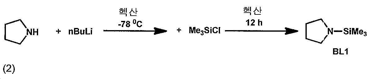
방응식 2는 BL1로서 언급된 1-트리메틸실릴피롤리딘에 대한 합성 반응식을 보여준다. 6.5 mL (80 mmol)의 피롤리딘을 250 mL 헥산에 용해시키고 용액을 -78 ℃로 냉각시켰다. 이러한 용액에 50 mL (80 mmol)의 헥산중 1.6 M n-부틸 리튬을 15 분의 기간에 걸쳐 적가하였다. 생성된 반응 혼합물이 서서히 실온에 도달하게 하고 30분 동안 교반하였다. 이어서 다시 반응 혼합물을 -78 ℃로 냉각하고, 10.1 mL (80 mmol) 트리메틸실릴 클로라이드를 함유하는 20 mL 헥산 용액을 10분의 기간에 걸쳐 첨가하였다. 반응 혼합물이 서서히 실온에 도달하게 하고 12 h 동안 교반하였다. 백색 침전물을 불활성 대기하에서 여과하고 헥산을 진공하에 증발시켰다. 생성물을 760 torr로 110 ℃에서 무색 액체로서 증류시켰다. 수율: 8.9 g (77.5 %). 1HNMR (400.18 MHz, C6D6) 2.87 (m, 4H), 1.57 (m, 4H), 0.11 (s, 9H) ppm; 13CNMR (100.64 MHz, C6D6) 1.08 ppm.Scheme 2 shows the synthetic scheme for 1-trimethylsilylpyrrolidine, referred to as BL1. 6.5 mL (80 mmol) of pyrrolidine was dissolved in 250 mL hexane and the solution was cooled to -78 °C. To this solution 50 mL (80 mmol) of 1.6 M n-butyl lithium in hexane was added dropwise over a period of 15 minutes. The resulting reaction mixture was allowed to gradually reach room temperature and stirred for 30 minutes. The reaction mixture was then cooled again to -78°C and 20 mL hexane solution containing 10.1 mL (80 mmol) trimethylsilyl chloride was added over a period of 10 minutes. The reaction mixture was allowed to slowly reach room temperature and stirred for 12 h. The white precipitate was filtered under inert atmosphere and the hexane was evaporated under vacuum. The product was distilled at 760 torr at 110° C. as a colorless liquid. Yield: 8.9 g (77.5%). 1 HNMR (400.18 MHz, C 6 D 6 ) 2.87 (m, 4H), 1.57 (m, 4H), 0.11 (s, 9H) ppm; 13 CNMR (100.64 MHz, C 6 D 6 ) 1.08 ppm.
1-트리메틸실릴피롤의 합성Synthesis of 1-trimethylsilylpyrrole
반응식 3은 BL2로서 또한 언급된 1-트리메틸실릴피롤의 합성 도식을 보여준다. 먼저 5.55 mL (80 mmol)의 피롤을 250 mL 헥산에 용해시키고 용액을 -78 ℃로 냉각시켰다. 이 용액에 50 mL (80 mmol)의 헥산 중 1.6 M n-부틸 리튬을 15 분의 기간에 걸쳐 적가하였다. 생성된 반응 혼합물이 서서히 실온을 획득하게 하고 30 분 동안 교반하였다. 이어서 반응 혼합물을 다시 -78 ℃로 냉각시키고, 10.1 mL (80 mmol) 트리메틸실릴 클로라이드의 20 mL 헥산 용액을 10 분의 기간에 걸쳐 첨가하였다. 반응 혼합물이 서서히 실온을 획득하게 하고 12 h 동안 교반하였다. 백색 침전물을 불활성 대기하에 여과하고 헥산을 진공하에 증발시켰다. 생성물을 760 torr로 130 ℃에서 무색 액체로서 증류시켰다. 수율: 8.7 g (78.2 %). 1HNMR (400.18 MHz, C6D6) 6.74 (s, 2H), 6.54 (s, 2H), 0.07 (s, 9H) ppm; 13CNMR (100.64 MHz, C6D6) 123.47, 112.20, -0.01 ppm. 질량 분광학: m/Z [M+H]+ 계산치 = 140.1, 실측치 140.2.Scheme 3 shows the synthetic scheme of 1-trimethylsilylpyrrole, also referred to as BL2. First, 5.55 mL (80 mmol) of pyrrole was dissolved in 250 mL hexane and the solution was cooled to -78 °C. To this solution 50 mL (80 mmol) of 1.6 M n-butyl lithium in hexane was added dropwise over a period of 15 minutes. The resulting reaction mixture was allowed to gradually acquire room temperature and stirred for 30 minutes. The reaction mixture was then cooled back to -78°C and a 20 mL hexane solution of 10.1 mL (80 mmol) trimethylsilyl chloride was added over a period of 10 minutes. The reaction mixture was allowed to gradually acquire room temperature and stirred for 12 h. The white precipitate was filtered under inert atmosphere and the hexane was evaporated under vacuum. The product was distilled at 760 torr at 130° C. as a colorless liquid. Yield: 8.7 g (78.2%). 1 HNMR (400.18 MHz, C 6 D 6 ) 6.74 (s, 2H), 6.54 (s, 2H), 0.07 (s, 9H) ppm; 13 CNMR (100.64 MHz, C 6 D 6 ) 123.47, 112.20, -0.01 ppm. Mass spectroscopy: m/Z [M+H] + calculated = 140.1, found 140.2.

3,5-디메틸-1-트리메틸실릴피라졸의 합성Synthesis of 3,5-dimethyl-1-trimethylsilylpyrazole
반응식 4는 BL3으로서 또한 언급된 3,5-디메틸-1-트리메틸실릴피라졸의 합성 도식을 보여준다. 7.7 g (80 mmol)의 3,5-디메틸 피라졸을 250 mL 헥산에 용해시키고, 용액을 -78 ℃로 냉각시켰다. 이 용액에, 50 mL (80 mmol)의 헥산 중 1.6 M n-부틸 리튬을 15분의 기간에 걸쳐 적가하였다. 생성된 반응 혼합물이 서서히 실온을 획득하게 하고 30분 동안 교반하였다. 이어서 반응 혼합물을 다시 -78 ℃로 냉각하고, 10.1 mL (80 mmol) 트리메틸실릴 클로라이드의 20 mL 헥산 용액을 10 분의 기간에 걸쳐 첨가하였다. 반응 혼합물이 서서히 실온을 획득하게 하고, 12 h 동안 교반하였다. 불활성 대기하에서 백색 침전물을 여과하고 헥산을 진공하에 증발시켰다. 생성물을 20 torr로 70 ℃에서 무색 액체로서 증류시켰다. 수율: 9.4 g (70.0 %). 1HNMR (400.18 MHz, C6D6) 5.80 (S, 1H), 2.30 (S, 3H), 2.00 (s, 3H), 0.32 (s, 9H) ppm; 13CNMR (100.64 MHz, C6D6) 151.97, 146.04, 108.40, 32.54, 23.63, 1.02 ppm. Scheme 4 shows the synthetic scheme of 3,5-dimethyl-1-trimethylsilylpyrazole, also referred to as BL3. 7.7 g (80 mmol) of 3,5-dimethyl pyrazole was dissolved in 250 mL hexane and the solution was cooled to -78 °C. To this solution, 50 mL (80 mmol) of 1.6 M n-butyl lithium in hexane was added dropwise over a period of 15 minutes. The resulting reaction mixture was allowed to gradually attain room temperature and stirred for 30 minutes. The reaction mixture was then cooled back to -78°C and a 20 mL hexane solution of 10.1 mL (80 mmol) trimethylsilyl chloride was added over a period of 10 minutes. The reaction mixture was allowed to gradually acquire room temperature and stirred for 12 h. The white precipitate was filtered off under an inert atmosphere and the hexane was evaporated under vacuum. The product was distilled at 20 torr at 70° C. as a colorless liquid. Yield: 9.4 g (70.0%). 1 HNMR (400.18 MHz, C 6 D 6 ) 5.80 (S, 1H), 2.30 (S, 3H), 2.00 (s, 3H), 0.32 (s, 9H) ppm; 13 CNMR (100.64 MHz, C 6 D 6 ) 151.97, 146.04, 108.40, 32.54, 23.63, 1.02 ppm.

1HNMR 및 13CNMR에 따라 합성 제조, 특징화 및 특성은 우수한 순도 및 높은 수율들을 입증하였다. TGA 분석에 따르면, 이들 분자들은 휘발성이며 (가장 높은 증발 속도는 90-137 ℃임) 및 열 안정적이며 잔류물이 ~0%이다.Synthetic preparation, characterization and characterization according to 1 HNMR and 13 CNMR demonstrated excellent purity and high yields. According to TGA analysis, these molecules are volatile (highest evaporation rate is 90-137 °C) and thermostable, with ~0% residue.
실시예Example
블록 층들로서의 트리메틸실릴아미드들을, 350 ℃에서 증기상에서 BL1으로 기판들 (Si(H), SiO2 1K, Si(천연 산화물))을 처리함으로써 평가하였다. 이어서 동일한 온도에서 SiN의 ALD를 수행하였다. 사용된 실리콘 전구체는 실리콘 테트라브로마이드 및 질소-함유 전구체 포함된 암모니아 (30T)였다. 총 100회 회전시켰다. 표 1은 BL1으로의 상이한 길이들의 2.4 Torr 침지로부터의 결과들을 보여준다. 표 2는 30초 동안 5 Torr 침지의 결과들을 보여준다.Trimethylsilylamides as block layers were evaluated by treating the substrates (Si(H), SiO 2 1K, Si(native oxide)) with BL1 in the vapor phase at 350° C. ALD of SiN was then performed at the same temperature. The silicon precursors used were ammonia (30T) with silicon tetrabromide and a nitrogen-containing precursor. It was rotated a total of 100 times. Table 1 shows the results from 2.4 Torr immersion of different lengths into BL1. Table 2 shows the results of 5 Torr immersion for 30 seconds.
표 1Table 1
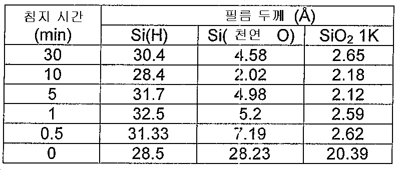
표 2Table 2

BL1을 전처리제로서 사용하지 않았을 경우, Si(H), SiO2 1K 및 Si(천연 O)와 관련한 선택성이 매우 조금 관찰되었다. 2T에서 1분 초과의 BL1 침지 시간은 매우 우수한 선택성을 가능하게 하였다. 접촉 각 측정들에 따르면, SiO2 및 Si(천연 O) 기판들 상에 SiN이 거의 또는 전혀 증착되지 않는다. 이는 Si(H) 상에서의 친수성 대 SiO2 및 Si(천연 O) 상에서의 소수성에 의해 입증되었다. 30 초의 BL1 침지 시간에서, 타원편광법을 기반으로 하는 일부 선택성이 여전히 존재하였으나, 접촉 각도들은 매우 유사하였으며, 이는 모두 3개의 표면들 상에 SiN이 존재함을 암시할 수 있다. 30초 동안 압력을 5T로 증가시키면 선택성을 회복하였다.When BL1 was not used as a pretreatment, very little selectivity was observed with respect to Si(H), SiO 2 1K and Si (native O). A BL1 soak time of >1 minute at 2T allowed very good selectivity. According to contact angle measurements, little or no SiN is deposited on SiO 2 and Si (native O) substrates. This was demonstrated by hydrophilicity on Si(H) versus hydrophobicity on SiO 2 and Si(native O). At a BL1 immersion time of 30 seconds, there was still some selectivity based on ellipsometry, but the contact angles were very similar, which could suggest the presence of SiN on all three surfaces. Selectivity was restored when the pressure was increased to 5T for 30 seconds.
회전 수의 함수로서 BL1의 선택성을 또한 평가하였다. 결과는 표 3에 수집하였다. 100회전 후, ~8.6 (Si(H) vs SiO2)의 선택성이 관찰되었다. 100회전 후, 선택성은 감소하는 것으로 나타났다. 임의의 특정 작업 이온에 제한되지 않으면서, BL1 블록 층이 약 100회전을 지속시키는 핵화 지연을 촉진하는 것으로 여겨진다.The selectivity of BL1 as a function of rotation number was also assessed. The results are collected in Table 3. After 100 rotations, a selectivity of ~8.6 (Si(H) vs SiO 2 ) was observed. After 100 rotations, selectivity appeared to decrease. Without being limited to any particular task ion, it is believed that the BL1 block layer promotes a nucleation delay lasting approximately 100 rotations.
표 3Table 3

상기 내용은 본 기재내용의 구체예들에 관한 것이나, 본 기재내용의 기타 및 추가의 구체예들이 이의 기본 범위로부터 벗어나지 않으면서 고안될 수 있으며, 이의 범위는 하기 청구범위에 의해 결정된다.Although the foregoing relates to embodiments of the present disclosure, other and additional embodiments of the present disclosure may be devised without departing from its basic scope, the scope of which is determined by the following claims.
Claims (15)
하이드록실-말단화된 표면을 포함하는 제 1 기판 표면 및 수소-말단화된 표면을 포함하는 제 2 기판 표면을 포함하는 기판을 제공하고;
기판을 실릴아미드에 노출하여 하이드록실-말단화된 표면과 반응시켜 실릴 에테르-말단화된 표면을 형성시키고;
기판을 하나 이상의 증착 가스들에 노출시켜 실릴 에테르 말단화된 표면에 비해 선택적으로 제 2 기판 표면 상에 필름을 증착시키는 것을 포함하고,
필름이 SiN을 포함하는 방법.As a method for depositing a film,
providing a substrate comprising a first substrate surface comprising a hydroxyl-terminated surface and a second substrate surface comprising a hydrogen-terminated surface;
exposing the substrate to silylamide to react with the hydroxyl-terminated surface to form a silyl ether-terminated surface;
depositing a film on a second substrate surface selectively relative to a silyl ether terminated surface by exposing the substrate to one or more deposition gases;
How the film incorporates SiN.
기판을 실릴아미드에 침지하여 하이드록실-말단화된 표면과 반응시켜 실릴 에테르-말단화된 표면을 형성하고;
기판을 하나 이상의 증착 가스들에 노출시켜 제 1 기판 표면에 비해 선택적으로 제 2 기판 표면 상에 실리콘 니트라이드 필름을 증착시키는 것을 포함하는 방법.A method of depositing a film, comprising: providing a substrate comprising a first substrate surface comprising a hydroxyl-terminated surface and a second substrate surface comprising a hydrogen-terminated dielectric;
dipping the substrate in silylamide to react with the hydroxyl-terminated surface to form a silyl ether-terminated surface;
A method comprising depositing a silicon nitride film selectively on a second substrate surface relative to a first substrate surface by exposing the substrate to one or more deposition gases.
Priority Applications (1)
| Application Number | Priority Date | Filing Date | Title |
|---|---|---|---|
| KR1020230121025A KR102712774B1 (en) | 2015-05-01 | 2023-09-12 | Selective deposition of thin film dielectrics using surface blocking chemistry |
Applications Claiming Priority (2)
| Application Number | Priority Date | Filing Date | Title |
|---|---|---|---|
| US201562155529P | 2015-05-01 | 2015-05-01 | |
| US62/155,529 | 2015-05-01 |
Related Child Applications (1)
| Application Number | Title | Priority Date | Filing Date |
|---|---|---|---|
| KR1020230121025A Division KR102712774B1 (en) | 2015-05-01 | 2023-09-12 | Selective deposition of thin film dielectrics using surface blocking chemistry |
Publications (2)
| Publication Number | Publication Date |
|---|---|
| KR20160130165A KR20160130165A (en) | 2016-11-10 |
| KR102579784B1 true KR102579784B1 (en) | 2023-09-15 |
Family
ID=57204153
Family Applications (2)
| Application Number | Title | Priority Date | Filing Date |
|---|---|---|---|
| KR1020160053287A Active KR102579784B1 (en) | 2015-05-01 | 2016-04-29 | Selective deposition of thin film dielectrics using surface blocking chemistry |
| KR1020230121025A Active KR102712774B1 (en) | 2015-05-01 | 2023-09-12 | Selective deposition of thin film dielectrics using surface blocking chemistry |
Family Applications After (1)
| Application Number | Title | Priority Date | Filing Date |
|---|---|---|---|
| KR1020230121025A Active KR102712774B1 (en) | 2015-05-01 | 2023-09-12 | Selective deposition of thin film dielectrics using surface blocking chemistry |
Country Status (6)
| Country | Link |
|---|---|
| US (2) | US9911591B2 (en) |
| JP (2) | JP6751107B2 (en) |
| KR (2) | KR102579784B1 (en) |
| CN (2) | CN107533951B (en) |
| TW (2) | TWI694167B (en) |
| WO (1) | WO2016178978A1 (en) |
Families Citing this family (76)
| Publication number | Priority date | Publication date | Assignee | Title |
|---|---|---|---|---|
| TWI739285B (en) | 2014-02-04 | 2021-09-11 | 荷蘭商Asm Ip控股公司 | Selective deposition of metals, metal oxides, and dielectrics |
| US10047435B2 (en) | 2014-04-16 | 2018-08-14 | Asm Ip Holding B.V. | Dual selective deposition |
| US9490145B2 (en) | 2015-02-23 | 2016-11-08 | Asm Ip Holding B.V. | Removal of surface passivation |
| TWI716333B (en) * | 2015-03-30 | 2021-01-11 | 法商液態空氣喬治斯克勞帝方法研究開發股份有限公司 | Catalyst dehydrogenative coupling of carbosilanes with ammonia, amnines and amidines |
| US10428421B2 (en) | 2015-08-03 | 2019-10-01 | Asm Ip Holding B.V. | Selective deposition on metal or metallic surfaces relative to dielectric surfaces |
| CN108028172B (en) * | 2015-09-19 | 2022-07-29 | 应用材料公司 | Surface selective atomic layer deposition using hydrosilylation passivation |
| US10695794B2 (en) | 2015-10-09 | 2020-06-30 | Asm Ip Holding B.V. | Vapor phase deposition of organic films |
| US10814349B2 (en) | 2015-10-09 | 2020-10-27 | Asm Ip Holding B.V. | Vapor phase deposition of organic films |
| US11081342B2 (en) | 2016-05-05 | 2021-08-03 | Asm Ip Holding B.V. | Selective deposition using hydrophobic precursors |
| US10373820B2 (en) | 2016-06-01 | 2019-08-06 | Asm Ip Holding B.V. | Deposition of organic films |
| US10453701B2 (en) | 2016-06-01 | 2019-10-22 | Asm Ip Holding B.V. | Deposition of organic films |
| US11430656B2 (en) | 2016-11-29 | 2022-08-30 | Asm Ip Holding B.V. | Deposition of oxide thin films |
| TWI700750B (en) * | 2017-01-24 | 2020-08-01 | 美商應用材料股份有限公司 | Method and apparatus for selective deposition of dielectric films |
| TWI739984B (en) | 2017-01-31 | 2021-09-21 | 美商應用材料股份有限公司 | Schemes for selective deposition for patterning applications |
| US10176984B2 (en) | 2017-02-14 | 2019-01-08 | Lam Research Corporation | Selective deposition of silicon oxide |
| JP7169072B2 (en) * | 2017-02-14 | 2022-11-10 | エーエスエム アイピー ホールディング ビー.ブイ. | Selective passivation and selective deposition |
| US10790140B2 (en) | 2017-02-14 | 2020-09-29 | Applied Materials, Inc. | High deposition rate and high quality nitride |
| US10242866B2 (en) * | 2017-03-08 | 2019-03-26 | Lam Research Corporation | Selective deposition of silicon nitride on silicon oxide using catalytic control |
| US10043656B1 (en) * | 2017-03-10 | 2018-08-07 | Lam Research Corporation | Selective growth of silicon oxide or silicon nitride on silicon surfaces in the presence of silicon oxide |
| WO2018170382A1 (en) * | 2017-03-17 | 2018-09-20 | Versum Materials Us, Llc | Selective deposition on silicon containing surfaces |
| US9911595B1 (en) | 2017-03-17 | 2018-03-06 | Lam Research Corporation | Selective growth of silicon nitride |
| US10559461B2 (en) | 2017-04-19 | 2020-02-11 | Lam Research Corporation | Selective deposition with atomic layer etch reset |
| US10355111B2 (en) | 2017-04-26 | 2019-07-16 | Taiwan Semiconductor Manufacturing Company, Ltd. | Deposition selectivity enhancement and manufacturing method thereof |
| US11501965B2 (en) | 2017-05-05 | 2022-11-15 | Asm Ip Holding B.V. | Plasma enhanced deposition processes for controlled formation of metal oxide thin films |
| KR102684628B1 (en) | 2017-05-16 | 2024-07-15 | 에이에스엠 아이피 홀딩 비.브이. | Selective PEALD of oxides on dielectrics |
| TWI782021B (en) * | 2017-05-28 | 2022-11-01 | 美商應用材料股份有限公司 | Selective molecular layer deposition of organic and hybrid organic-inorganic layers |
| KR102331718B1 (en) | 2017-06-08 | 2021-11-26 | 삼성전자주식회사 | Methods of manufacturing a semiconductor device |
| TWI722301B (en) | 2017-07-18 | 2021-03-21 | 美商應用材料股份有限公司 | Methods for depositing blocking layers on metal material surfaces |
| US10515896B2 (en) * | 2017-08-31 | 2019-12-24 | Taiwan Semiconductor Manufacturing Co., Ltd. | Interconnect structure for semiconductor device and methods of fabrication thereof |
| WO2019055508A1 (en) * | 2017-09-12 | 2019-03-21 | Applied Materials, Inc. | Selective deposition defects removal by chemical etch |
| CN111108232A (en) * | 2017-09-19 | 2020-05-05 | 应用材料公司 | Method for selective deposition of dielectrics on silicon dioxide |
| US10403504B2 (en) * | 2017-10-05 | 2019-09-03 | Asm Ip Holding B.V. | Method for selectively depositing a metallic film on a substrate |
| US11515151B2 (en) * | 2017-10-06 | 2022-11-29 | Applied Materials, Inc. | Methods and precursors for selective deposition of metal films |
| JP6956592B2 (en) * | 2017-10-31 | 2021-11-02 | 東京エレクトロン株式会社 | Methods and equipment for forming silicon oxide films |
| US10460930B2 (en) | 2017-11-22 | 2019-10-29 | Lam Research Corporation | Selective growth of SiO2 on dielectric surfaces in the presence of copper |
| SG11202005432RA (en) * | 2017-12-17 | 2020-07-29 | Applied Materials Inc | Silicide films through selective deposition |
| US11404275B2 (en) | 2018-03-02 | 2022-08-02 | Lam Research Corporation | Selective deposition using hydrolysis |
| KR102652331B1 (en) | 2018-04-13 | 2024-03-29 | 어플라이드 머티어리얼스, 인코포레이티드 | Methods of selective atomic layer deposition |
| SG11202011847TA (en) * | 2018-05-28 | 2020-12-30 | Kokusai Electric Corp | Method of manufacturing semiconductor device, substrate processing apparatus, and program |
| US11069526B2 (en) * | 2018-06-27 | 2021-07-20 | Taiwan Semiconductor Manufacturing Co., Ltd. | Using a self-assembly layer to facilitate selective formation of an etching stop layer |
| KR102640002B1 (en) * | 2018-07-17 | 2024-02-27 | 가부시키가이샤 코쿠사이 엘렉트릭 | Semiconductor device manufacturing method, substrate processing apparatus, recording medium, and program |
| KR102637397B1 (en) * | 2018-07-17 | 2024-02-16 | 가부시키가이샤 코쿠사이 엘렉트릭 | Substrate processing method, substrate processing apparatus, program and method of manufacturing semiconductor device |
| SG11202101696UA (en) * | 2018-08-27 | 2021-03-30 | Versum Materials Us Llc | Selective deposition on silicon containing surfaces |
| US10665715B2 (en) | 2018-08-28 | 2020-05-26 | International Business Machines Corporation | Controlling gate length of vertical transistors |
| US10840133B2 (en) | 2018-09-27 | 2020-11-17 | Taiwan Semiconductor Manufacturing Co., Ltd. | Semiconductor structure with staggered selective growth |
| DE102019109846A1 (en) | 2018-09-27 | 2020-04-02 | Taiwan Semiconductor Manufacturing Co., Ltd. | SEMICONDUCTOR STRUCTURE WITH STAGE SELECTIVE GROWTH |
| US10662526B2 (en) * | 2018-10-02 | 2020-05-26 | Lam Research Corporation | Method for selective deposition using a base-catalyzed inhibitor |
| US12482648B2 (en) | 2018-10-02 | 2025-11-25 | Asm Ip Holding B.V. | Selective passivation and selective deposition |
| JP2020056104A (en) | 2018-10-02 | 2020-04-09 | エーエスエム アイピー ホールディング ビー.ブイ. | Selective passivation and selective deposition |
| US10692755B2 (en) | 2018-10-24 | 2020-06-23 | International Business Machines Corporation | Selective deposition of dielectrics on ultra-low k dielectrics |
| US10886462B2 (en) | 2018-11-19 | 2021-01-05 | International Business Machines Corporation | Encapsulated memory pillars |
| TWI757659B (en) * | 2018-11-23 | 2022-03-11 | 美商應用材料股份有限公司 | Selective deposition of carbon films and uses thereof |
| WO2020145269A1 (en) * | 2019-01-10 | 2020-07-16 | セントラル硝子株式会社 | Substrate, selective film deposition method, deposition film of organic matter, and organic matter |
| CN113423864B (en) * | 2019-02-14 | 2023-11-07 | 恩特格里斯公司 | Selective deposition of silicon nitride |
| JP6860605B2 (en) * | 2019-03-18 | 2021-04-14 | 株式会社Kokusai Electric | Semiconductor device manufacturing methods, substrate processing devices, and programs |
| US11965238B2 (en) | 2019-04-12 | 2024-04-23 | Asm Ip Holding B.V. | Selective deposition of metal oxides on metal surfaces |
| JP6953480B2 (en) * | 2019-07-31 | 2021-10-27 | 株式会社Kokusai Electric | Semiconductor device manufacturing methods, substrate processing devices, and programs |
| US11139163B2 (en) | 2019-10-31 | 2021-10-05 | Asm Ip Holding B.V. | Selective deposition of SiOC thin films |
| JP7227122B2 (en) | 2019-12-27 | 2023-02-21 | 株式会社Kokusai Electric | Substrate processing method, semiconductor device manufacturing method, substrate processing apparatus, and program |
| JP7254044B2 (en) * | 2020-03-25 | 2023-04-07 | 株式会社Kokusai Electric | Substrate processing method, semiconductor device manufacturing method, substrate processing apparatus, and program |
| TW202140832A (en) | 2020-03-30 | 2021-11-01 | 荷蘭商Asm Ip私人控股有限公司 | Selective deposition of silicon oxide on metal surfaces |
| TWI865747B (en) | 2020-03-30 | 2024-12-11 | 荷蘭商Asm Ip私人控股有限公司 | Simultaneous selective deposition of two different materials on two different surfaces |
| TWI862807B (en) | 2020-03-30 | 2024-11-21 | 荷蘭商Asm Ip私人控股有限公司 | Selective deposition of silicon oxide on dielectric surfaces relative to metal surfaces |
| US11930637B2 (en) | 2020-06-19 | 2024-03-12 | Applied Materials, Inc. | Confined charge trap layer |
| US20220127717A1 (en) * | 2020-10-27 | 2022-04-28 | Applied Materials, Inc. | Selective Deposition Of A Heterocyclic Passivation Film On A Metal Surface |
| TW202235649A (en) * | 2020-11-24 | 2022-09-16 | 荷蘭商Asm Ip私人控股有限公司 | Methods for filling a gap and related systems and devices |
| US20240170283A1 (en) * | 2021-03-02 | 2024-05-23 | Versum Materials Us, Llc | Selective deposition of silicon dielectric film |
| US11756790B2 (en) * | 2021-03-09 | 2023-09-12 | Tokyo Electron Limited | Method for patterning a dielectric layer |
| JP7339975B2 (en) | 2021-03-18 | 2023-09-06 | 株式会社Kokusai Electric | SUBSTRATE PROCESSING METHOD, SEMICONDUCTOR DEVICE MANUFACTURING METHOD, SUBSTRATE PROCESSING APPARATUS, AND PROGRAM |
| US11702733B2 (en) | 2021-05-07 | 2023-07-18 | Applied Materials, Inc. | Methods for depositing blocking layers on conductive surfaces |
| TW202325887A (en) * | 2021-10-29 | 2023-07-01 | 荷蘭商Asm Ip私人控股有限公司 | Selective deposition of material comprising silicon and oxygen using plasma |
| US12476144B2 (en) | 2021-12-07 | 2025-11-18 | International Business Machines Corporation | Etch back and film profile shaping of selective dielectric deposition |
| KR20240008788A (en) | 2022-07-11 | 2024-01-19 | 에이에스엠 아이피 홀딩 비.브이. | Method for selective deposition of silicon nitride and structure including selectively-deposited silicon nitride layer |
| US20250081593A1 (en) * | 2023-09-01 | 2025-03-06 | Applied Materials ,Inc | Methods of improving pmos transistor performance |
| KR102830634B1 (en) * | 2023-12-20 | 2025-07-07 | 에스케이스페셜티 주식회사 | Deposition method of silicon oxide film on a semiconductor substrate and preparing method of semiconductor device comprising the same |
| CN121463738A (en) * | 2024-07-29 | 2026-02-03 | 株式会社国际电气 | Substrate processing method, semiconductor device manufacturing method, recording medium, and substrate processing apparatus |
Citations (6)
| Publication number | Priority date | Publication date | Assignee | Title |
|---|---|---|---|---|
| JP2001286768A (en) * | 2000-02-02 | 2001-10-16 | Sumitomo Chem Co Ltd | Molded catalyst, method for producing molded catalyst, and method for producing oxirane compound |
| US20030083189A1 (en) | 2000-02-02 | 2003-05-01 | Jun Yamamoto | Molded catalyst, process for producing molded catalyst, and process for producing oxirane compound |
| US20050208760A1 (en) | 2003-07-31 | 2005-09-22 | Advanced Micro Devices, Inc. | Interconnects with a dielectric sealant layer |
| US20060199399A1 (en) | 2005-02-22 | 2006-09-07 | Muscat Anthony J | Surface manipulation and selective deposition processes using adsorbed halogen atoms |
| WO2012002440A1 (en) * | 2010-06-29 | 2012-01-05 | 京セラ株式会社 | Method for surface-treating semiconductor substrate, semiconductor substrate, and method for producing solar battery |
| US20120196451A1 (en) | 2010-09-10 | 2012-08-02 | Applied Materials, Inc. | Embedded catalyst for atomic layer deposition of silicon oxide |
Family Cites Families (30)
| Publication number | Priority date | Publication date | Assignee | Title |
|---|---|---|---|---|
| JP2574822B2 (en) * | 1987-12-07 | 1997-01-22 | 株式会社日立製作所 | Method for manufacturing semiconductor device |
| JP3489299B2 (en) * | 1995-04-21 | 2004-01-19 | 株式会社デンソー | Surface modification equipment |
| EP0809282A1 (en) * | 1996-04-26 | 1997-11-26 | Max-Planck-Gesellschaft zur Förderung der Wissenschaften e.V. | A method for treating a substrate surface, a method for producing an at least partially metallized substrate and a substrate having a treated surface |
| US6077643A (en) * | 1997-08-28 | 2000-06-20 | Shipley Company, L.L.C. | Polymers and photoresist compositions |
| CN1240237A (en) * | 1998-06-10 | 2000-01-05 | 陶氏康宁公司 | Electroless metal deposition on silyl hydride functional resin |
| US6200893B1 (en) | 1999-03-11 | 2001-03-13 | Genus, Inc | Radical-assisted sequential CVD |
| US6660660B2 (en) * | 2000-10-10 | 2003-12-09 | Asm International, Nv. | Methods for making a dielectric stack in an integrated circuit |
| US20090004850A1 (en) * | 2001-07-25 | 2009-01-01 | Seshadri Ganguli | Process for forming cobalt and cobalt silicide materials in tungsten contact applications |
| JP3820975B2 (en) * | 2001-12-12 | 2006-09-13 | ソニー株式会社 | Semiconductor device and manufacturing method thereof |
| US6930059B2 (en) * | 2003-02-27 | 2005-08-16 | Sharp Laboratories Of America, Inc. | Method for depositing a nanolaminate film by atomic layer deposition |
| US7132360B2 (en) * | 2004-06-10 | 2006-11-07 | Freescale Semiconductor, Inc. | Method for treating a semiconductor surface to form a metal-containing layer |
| US8575021B2 (en) * | 2004-11-22 | 2013-11-05 | Intermolecular, Inc. | Substrate processing including a masking layer |
| US8029698B2 (en) * | 2005-04-19 | 2011-10-04 | The Research Foundation Of State University Of New York | Production of photoluminescent silicon nanoparticles having surfaces that are essentially free of residual oxygen |
| JP2007145984A (en) * | 2005-11-28 | 2007-06-14 | Sharp Corp | Siloxane-based molecular film, method for producing the same, and organic device using the film |
| JP5412294B2 (en) * | 2007-02-14 | 2014-02-12 | 本田技研工業株式会社 | Fabrication method of spatially dispersed nanostructures controlled in size by atomic layer deposition |
| GB2459604B (en) * | 2007-02-26 | 2011-07-06 | Wisconsin Alumni Res Found | Surface plasmon resonance compatible carbon thin films |
| WO2008123141A1 (en) | 2007-03-23 | 2008-10-16 | Asahi Kasei Emd Corporation | Compound semiconductor laminate, process for producing the compound semiconductor laminate, and semiconductor device |
| US7763399B2 (en) * | 2007-08-31 | 2010-07-27 | Intel Corporation | Removal of ionic residues or oxides and prevention of photo-induced defects, ionic crystal or oxide growth on photolithographic surfaces |
| US8242019B2 (en) | 2009-03-31 | 2012-08-14 | Tokyo Electron Limited | Selective deposition of metal-containing cap layers for semiconductor devices |
| KR101096031B1 (en) * | 2009-03-31 | 2011-12-19 | 한양대학교 산학협력단 | Method of forming self-assembled monolayer and copper wiring of semiconductor device using same |
| US8230720B2 (en) * | 2009-11-19 | 2012-07-31 | Honeywell International Inc. | Functionalized monolayers for carbon dioxide detection by a resonant nanosensor |
| US8293658B2 (en) | 2010-02-17 | 2012-10-23 | Asm America, Inc. | Reactive site deactivation against vapor deposition |
| US20110308603A1 (en) * | 2010-06-17 | 2011-12-22 | Katholieke Universiteit Leuven | Method for passivating a silicon surface |
| US20120213940A1 (en) * | 2010-10-04 | 2012-08-23 | Applied Materials, Inc. | Atomic layer deposition of silicon nitride using dual-source precursor and interleaved plasma |
| US20120201959A1 (en) * | 2011-02-04 | 2012-08-09 | Applied Materials, Inc. | In-Situ Hydroxylation System |
| US8778816B2 (en) * | 2011-02-04 | 2014-07-15 | Applied Materials, Inc. | In situ vapor phase surface activation of SiO2 |
| US8728955B2 (en) * | 2012-02-14 | 2014-05-20 | Novellus Systems, Inc. | Method of plasma activated deposition of a conformal film on a substrate surface |
| US9443736B2 (en) | 2012-05-25 | 2016-09-13 | Entegris, Inc. | Silylene compositions and methods of use thereof |
| US10047435B2 (en) | 2014-04-16 | 2018-08-14 | Asm Ip Holding B.V. | Dual selective deposition |
| KR102185458B1 (en) | 2015-02-03 | 2020-12-03 | 에이에스엠 아이피 홀딩 비.브이. | Selective deposition |
-
2016
- 2016-04-29 US US15/142,497 patent/US9911591B2/en active Active
- 2016-04-29 WO PCT/US2016/030057 patent/WO2016178978A1/en not_active Ceased
- 2016-04-29 TW TW105113504A patent/TWI694167B/en active
- 2016-04-29 CN CN201680025233.4A patent/CN107533951B/en active Active
- 2016-04-29 KR KR1020160053287A patent/KR102579784B1/en active Active
- 2016-04-29 JP JP2017557135A patent/JP6751107B2/en active Active
- 2016-04-29 CN CN202111203384.3A patent/CN113936994B/en active Active
- 2016-04-29 TW TW109112760A patent/TWI717260B/en active
-
2018
- 2018-03-05 US US15/912,388 patent/US10219373B2/en active Active
-
2020
- 2020-08-13 JP JP2020136639A patent/JP7087031B2/en active Active
-
2023
- 2023-09-12 KR KR1020230121025A patent/KR102712774B1/en active Active
Patent Citations (6)
| Publication number | Priority date | Publication date | Assignee | Title |
|---|---|---|---|---|
| JP2001286768A (en) * | 2000-02-02 | 2001-10-16 | Sumitomo Chem Co Ltd | Molded catalyst, method for producing molded catalyst, and method for producing oxirane compound |
| US20030083189A1 (en) | 2000-02-02 | 2003-05-01 | Jun Yamamoto | Molded catalyst, process for producing molded catalyst, and process for producing oxirane compound |
| US20050208760A1 (en) | 2003-07-31 | 2005-09-22 | Advanced Micro Devices, Inc. | Interconnects with a dielectric sealant layer |
| US20060199399A1 (en) | 2005-02-22 | 2006-09-07 | Muscat Anthony J | Surface manipulation and selective deposition processes using adsorbed halogen atoms |
| WO2012002440A1 (en) * | 2010-06-29 | 2012-01-05 | 京セラ株式会社 | Method for surface-treating semiconductor substrate, semiconductor substrate, and method for producing solar battery |
| US20120196451A1 (en) | 2010-09-10 | 2012-08-02 | Applied Materials, Inc. | Embedded catalyst for atomic layer deposition of silicon oxide |
Also Published As
| Publication number | Publication date |
|---|---|
| TW202043524A (en) | 2020-12-01 |
| US20180199432A1 (en) | 2018-07-12 |
| WO2016178978A1 (en) | 2016-11-10 |
| JP6751107B2 (en) | 2020-09-02 |
| KR20160130165A (en) | 2016-11-10 |
| US20160322213A1 (en) | 2016-11-03 |
| US9911591B2 (en) | 2018-03-06 |
| US10219373B2 (en) | 2019-02-26 |
| CN107533951A (en) | 2018-01-02 |
| CN107533951B (en) | 2021-10-26 |
| JP2018523289A (en) | 2018-08-16 |
| JP7087031B2 (en) | 2022-06-20 |
| KR20230132760A (en) | 2023-09-18 |
| TW201700768A (en) | 2017-01-01 |
| CN113936994A (en) | 2022-01-14 |
| TWI694167B (en) | 2020-05-21 |
| TWI717260B (en) | 2021-01-21 |
| JP2020205429A (en) | 2020-12-24 |
| KR102712774B1 (en) | 2024-09-30 |
| CN113936994B (en) | 2025-11-07 |
Similar Documents
| Publication | Publication Date | Title |
|---|---|---|
| KR102712774B1 (en) | Selective deposition of thin film dielectrics using surface blocking chemistry | |
| CN108028172B (en) | Surface selective atomic layer deposition using hydrosilylation passivation | |
| US11028478B2 (en) | Atomic layer deposition of films comprising silicon, carbon and nitrogen using halogenated silicon precursors | |
| US9685325B2 (en) | Carbon and/or nitrogen incorporation in silicon based films using silicon precursors with organic co-reactants by PE-ALD | |
| US20180025907A1 (en) | Deposition Of Flowable Silicon-Containing Films | |
| JP6968701B2 (en) | A method for depositing a dielectric thin film with a low dielectric constant and a low wet etching rate. | |
| US9875889B2 (en) | Atomic layer deposition of films comprising Si(C)N using hydrazine, azide and/or silyl amine derivatives | |
| KR20150121217A (en) | LOW TEMPERATURE ATOMIC LAYER DEPOSITION OF FILMS COMPRISING SiCN OR SiCON | |
| KR20240003451A (en) | Methods of Forming Molybdenum Contacts | |
| US9177783B2 (en) | Substituted silacyclopropane precursors and their use for the deposition of silicon-containing films | |
| US12387927B2 (en) | Deposition of boron films | |
| TWI640651B (en) | Atomic layer deposition of films comprising silicon, carbon and nitrogen using halogenated silicon precursors | |
| TWI876179B (en) | Novel oxidants and strained-ring precursors |
Legal Events
| Date | Code | Title | Description |
|---|---|---|---|
| E13-X000 | Pre-grant limitation requested |
St.27 status event code: A-2-3-E10-E13-lim-X000 |
|
| PA0109 | Patent application |
St.27 status event code: A-0-1-A10-A12-nap-PA0109 |
|
| PG1501 | Laying open of application |
St.27 status event code: A-1-1-Q10-Q12-nap-PG1501 |
|
| A201 | Request for examination | ||
| PA0201 | Request for examination |
St.27 status event code: A-1-2-D10-D11-exm-PA0201 |
|
| E902 | Notification of reason for refusal | ||
| PE0902 | Notice of grounds for rejection |
St.27 status event code: A-1-2-D10-D21-exm-PE0902 |
|
| E13-X000 | Pre-grant limitation requested |
St.27 status event code: A-2-3-E10-E13-lim-X000 |
|
| P11-X000 | Amendment of application requested |
St.27 status event code: A-2-2-P10-P11-nap-X000 |
|
| P13-X000 | Application amended |
St.27 status event code: A-2-2-P10-P13-nap-X000 |
|
| E701 | Decision to grant or registration of patent right | ||
| PE0701 | Decision of registration |
St.27 status event code: A-1-2-D10-D22-exm-PE0701 |
|
| A107 | Divisional application of patent | ||
| PA0107 | Divisional application |
St.27 status event code: A-0-1-A10-A18-div-PA0107 St.27 status event code: A-0-1-A10-A16-div-PA0107 |
|
| GRNT | Written decision to grant | ||
| PR0701 | Registration of establishment |
St.27 status event code: A-2-4-F10-F11-exm-PR0701 |
|
| PR1002 | Payment of registration fee |
St.27 status event code: A-2-2-U10-U11-oth-PR1002 Fee payment year number: 1 |
|
| PG1601 | Publication of registration |
St.27 status event code: A-4-4-Q10-Q13-nap-PG1601 |
|
| R17 | Change to representative recorded |
Free format text: ST27 STATUS EVENT CODE: A-5-5-R10-R17-OTH-X000 (AS PROVIDED BY THE NATIONAL OFFICE) |
|
| R17-X000 | Change to representative recorded |
St.27 status event code: A-5-5-R10-R17-oth-X000 |
|
| P22-X000 | Classification modified |
St.27 status event code: A-4-4-P10-P22-nap-X000 |