KR102547871B1 - 화소 및 이를 가지는 유기전계발광 표시장치 - Google Patents
화소 및 이를 가지는 유기전계발광 표시장치 Download PDFInfo
- Publication number
- KR102547871B1 KR102547871B1 KR1020160162995A KR20160162995A KR102547871B1 KR 102547871 B1 KR102547871 B1 KR 102547871B1 KR 1020160162995 A KR1020160162995 A KR 1020160162995A KR 20160162995 A KR20160162995 A KR 20160162995A KR 102547871 B1 KR102547871 B1 KR 102547871B1
- Authority
- KR
- South Korea
- Prior art keywords
- transistor
- pixel
- turned
- node
- voltage
- Prior art date
- Legal status (The legal status is an assumption and is not a legal conclusion. Google has not performed a legal analysis and makes no representation as to the accuracy of the status listed.)
- Active
Links
- 230000006641 stabilisation Effects 0.000 claims abstract description 237
- 238000011105 stabilization Methods 0.000 claims abstract description 237
- 239000003990 capacitor Substances 0.000 claims abstract description 70
- 239000004065 semiconductor Substances 0.000 claims description 132
- 229910021420 polycrystalline silicon Inorganic materials 0.000 claims description 62
- 229920005591 polysilicon Polymers 0.000 claims description 61
- 238000000034 method Methods 0.000 claims description 47
- 238000010586 diagram Methods 0.000 description 49
- 229910013756 M(PN) Inorganic materials 0.000 description 16
- 229910013763 M(PP) Inorganic materials 0.000 description 16
- 238000012986 modification Methods 0.000 description 2
- 230000004048 modification Effects 0.000 description 2
- 238000005070 sampling Methods 0.000 description 2
- 239000004973 liquid crystal related substance Substances 0.000 description 1
- 230000003071 parasitic effect Effects 0.000 description 1
- 238000005215 recombination Methods 0.000 description 1
- 230000006798 recombination Effects 0.000 description 1
- 230000000087 stabilizing effect Effects 0.000 description 1
- 239000000758 substrate Substances 0.000 description 1
- 239000010409 thin film Substances 0.000 description 1
Images


Classifications
-
- G—PHYSICS
- G09—EDUCATION; CRYPTOGRAPHY; DISPLAY; ADVERTISING; SEALS
- G09G—ARRANGEMENTS OR CIRCUITS FOR CONTROL OF INDICATING DEVICES USING STATIC MEANS TO PRESENT VARIABLE INFORMATION
- G09G3/00—Control arrangements or circuits, of interest only in connection with visual indicators other than cathode-ray tubes
- G09G3/20—Control arrangements or circuits, of interest only in connection with visual indicators other than cathode-ray tubes for presentation of an assembly of a number of characters, e.g. a page, by composing the assembly by combination of individual elements arranged in a matrix no fixed position being assigned to or needed to be assigned to the individual characters or partial characters
- G09G3/22—Control arrangements or circuits, of interest only in connection with visual indicators other than cathode-ray tubes for presentation of an assembly of a number of characters, e.g. a page, by composing the assembly by combination of individual elements arranged in a matrix no fixed position being assigned to or needed to be assigned to the individual characters or partial characters using controlled light sources
- G09G3/30—Control arrangements or circuits, of interest only in connection with visual indicators other than cathode-ray tubes for presentation of an assembly of a number of characters, e.g. a page, by composing the assembly by combination of individual elements arranged in a matrix no fixed position being assigned to or needed to be assigned to the individual characters or partial characters using controlled light sources using electroluminescent panels
- G09G3/32—Control arrangements or circuits, of interest only in connection with visual indicators other than cathode-ray tubes for presentation of an assembly of a number of characters, e.g. a page, by composing the assembly by combination of individual elements arranged in a matrix no fixed position being assigned to or needed to be assigned to the individual characters or partial characters using controlled light sources using electroluminescent panels semiconductive, e.g. using light-emitting diodes [LED]
- G09G3/3208—Control arrangements or circuits, of interest only in connection with visual indicators other than cathode-ray tubes for presentation of an assembly of a number of characters, e.g. a page, by composing the assembly by combination of individual elements arranged in a matrix no fixed position being assigned to or needed to be assigned to the individual characters or partial characters using controlled light sources using electroluminescent panels semiconductive, e.g. using light-emitting diodes [LED] organic, e.g. using organic light-emitting diodes [OLED]
- G09G3/3225—Control arrangements or circuits, of interest only in connection with visual indicators other than cathode-ray tubes for presentation of an assembly of a number of characters, e.g. a page, by composing the assembly by combination of individual elements arranged in a matrix no fixed position being assigned to or needed to be assigned to the individual characters or partial characters using controlled light sources using electroluminescent panels semiconductive, e.g. using light-emitting diodes [LED] organic, e.g. using organic light-emitting diodes [OLED] using an active matrix
- G09G3/3233—Control arrangements or circuits, of interest only in connection with visual indicators other than cathode-ray tubes for presentation of an assembly of a number of characters, e.g. a page, by composing the assembly by combination of individual elements arranged in a matrix no fixed position being assigned to or needed to be assigned to the individual characters or partial characters using controlled light sources using electroluminescent panels semiconductive, e.g. using light-emitting diodes [LED] organic, e.g. using organic light-emitting diodes [OLED] using an active matrix with pixel circuitry controlling the current through the light-emitting element
-
- G—PHYSICS
- G09—EDUCATION; CRYPTOGRAPHY; DISPLAY; ADVERTISING; SEALS
- G09G—ARRANGEMENTS OR CIRCUITS FOR CONTROL OF INDICATING DEVICES USING STATIC MEANS TO PRESENT VARIABLE INFORMATION
- G09G3/00—Control arrangements or circuits, of interest only in connection with visual indicators other than cathode-ray tubes
- G09G3/20—Control arrangements or circuits, of interest only in connection with visual indicators other than cathode-ray tubes for presentation of an assembly of a number of characters, e.g. a page, by composing the assembly by combination of individual elements arranged in a matrix no fixed position being assigned to or needed to be assigned to the individual characters or partial characters
- G09G3/22—Control arrangements or circuits, of interest only in connection with visual indicators other than cathode-ray tubes for presentation of an assembly of a number of characters, e.g. a page, by composing the assembly by combination of individual elements arranged in a matrix no fixed position being assigned to or needed to be assigned to the individual characters or partial characters using controlled light sources
- G09G3/30—Control arrangements or circuits, of interest only in connection with visual indicators other than cathode-ray tubes for presentation of an assembly of a number of characters, e.g. a page, by composing the assembly by combination of individual elements arranged in a matrix no fixed position being assigned to or needed to be assigned to the individual characters or partial characters using controlled light sources using electroluminescent panels
- G09G3/32—Control arrangements or circuits, of interest only in connection with visual indicators other than cathode-ray tubes for presentation of an assembly of a number of characters, e.g. a page, by composing the assembly by combination of individual elements arranged in a matrix no fixed position being assigned to or needed to be assigned to the individual characters or partial characters using controlled light sources using electroluminescent panels semiconductive, e.g. using light-emitting diodes [LED]
- G09G3/3208—Control arrangements or circuits, of interest only in connection with visual indicators other than cathode-ray tubes for presentation of an assembly of a number of characters, e.g. a page, by composing the assembly by combination of individual elements arranged in a matrix no fixed position being assigned to or needed to be assigned to the individual characters or partial characters using controlled light sources using electroluminescent panels semiconductive, e.g. using light-emitting diodes [LED] organic, e.g. using organic light-emitting diodes [OLED]
- G09G3/3225—Control arrangements or circuits, of interest only in connection with visual indicators other than cathode-ray tubes for presentation of an assembly of a number of characters, e.g. a page, by composing the assembly by combination of individual elements arranged in a matrix no fixed position being assigned to or needed to be assigned to the individual characters or partial characters using controlled light sources using electroluminescent panels semiconductive, e.g. using light-emitting diodes [LED] organic, e.g. using organic light-emitting diodes [OLED] using an active matrix
- G09G3/3258—Control arrangements or circuits, of interest only in connection with visual indicators other than cathode-ray tubes for presentation of an assembly of a number of characters, e.g. a page, by composing the assembly by combination of individual elements arranged in a matrix no fixed position being assigned to or needed to be assigned to the individual characters or partial characters using controlled light sources using electroluminescent panels semiconductive, e.g. using light-emitting diodes [LED] organic, e.g. using organic light-emitting diodes [OLED] using an active matrix with pixel circuitry controlling the voltage across the light-emitting element
-
- G—PHYSICS
- G09—EDUCATION; CRYPTOGRAPHY; DISPLAY; ADVERTISING; SEALS
- G09G—ARRANGEMENTS OR CIRCUITS FOR CONTROL OF INDICATING DEVICES USING STATIC MEANS TO PRESENT VARIABLE INFORMATION
- G09G2300/00—Aspects of the constitution of display devices
- G09G2300/04—Structural and physical details of display devices
- G09G2300/0421—Structural details of the set of electrodes
- G09G2300/0426—Layout of electrodes and connections
-
- G—PHYSICS
- G09—EDUCATION; CRYPTOGRAPHY; DISPLAY; ADVERTISING; SEALS
- G09G—ARRANGEMENTS OR CIRCUITS FOR CONTROL OF INDICATING DEVICES USING STATIC MEANS TO PRESENT VARIABLE INFORMATION
- G09G2300/00—Aspects of the constitution of display devices
- G09G2300/08—Active matrix structure, i.e. with use of active elements, inclusive of non-linear two terminal elements, in the pixels together with light emitting or modulating elements
- G09G2300/0809—Several active elements per pixel in active matrix panels
- G09G2300/0819—Several active elements per pixel in active matrix panels used for counteracting undesired variations, e.g. feedback or autozeroing
-
- G—PHYSICS
- G09—EDUCATION; CRYPTOGRAPHY; DISPLAY; ADVERTISING; SEALS
- G09G—ARRANGEMENTS OR CIRCUITS FOR CONTROL OF INDICATING DEVICES USING STATIC MEANS TO PRESENT VARIABLE INFORMATION
- G09G2300/00—Aspects of the constitution of display devices
- G09G2300/08—Active matrix structure, i.e. with use of active elements, inclusive of non-linear two terminal elements, in the pixels together with light emitting or modulating elements
- G09G2300/0809—Several active elements per pixel in active matrix panels
- G09G2300/0842—Several active elements per pixel in active matrix panels forming a memory circuit, e.g. a dynamic memory with one capacitor
- G09G2300/0852—Several active elements per pixel in active matrix panels forming a memory circuit, e.g. a dynamic memory with one capacitor being a dynamic memory with more than one capacitor
-
- G—PHYSICS
- G09—EDUCATION; CRYPTOGRAPHY; DISPLAY; ADVERTISING; SEALS
- G09G—ARRANGEMENTS OR CIRCUITS FOR CONTROL OF INDICATING DEVICES USING STATIC MEANS TO PRESENT VARIABLE INFORMATION
- G09G2310/00—Command of the display device
- G09G2310/02—Addressing, scanning or driving the display screen or processing steps related thereto
- G09G2310/0202—Addressing of scan or signal lines
- G09G2310/0216—Interleaved control phases for different scan lines in the same sub-field, e.g. initialization, addressing and sustaining in plasma displays that are not simultaneous for all scan lines
-
- G—PHYSICS
- G09—EDUCATION; CRYPTOGRAPHY; DISPLAY; ADVERTISING; SEALS
- G09G—ARRANGEMENTS OR CIRCUITS FOR CONTROL OF INDICATING DEVICES USING STATIC MEANS TO PRESENT VARIABLE INFORMATION
- G09G2310/00—Command of the display device
- G09G2310/08—Details of timing specific for flat panels, other than clock recovery
-
- G—PHYSICS
- G09—EDUCATION; CRYPTOGRAPHY; DISPLAY; ADVERTISING; SEALS
- G09G—ARRANGEMENTS OR CIRCUITS FOR CONTROL OF INDICATING DEVICES USING STATIC MEANS TO PRESENT VARIABLE INFORMATION
- G09G2320/00—Control of display operating conditions
- G09G2320/02—Improving the quality of display appearance
- G09G2320/0209—Crosstalk reduction, i.e. to reduce direct or indirect influences of signals directed to a certain pixel of the displayed image on other pixels of said image, inclusive of influences affecting pixels in different frames or fields or sub-images which constitute a same image, e.g. left and right images of a stereoscopic display
- G09G2320/0214—Crosstalk reduction, i.e. to reduce direct or indirect influences of signals directed to a certain pixel of the displayed image on other pixels of said image, inclusive of influences affecting pixels in different frames or fields or sub-images which constitute a same image, e.g. left and right images of a stereoscopic display with crosstalk due to leakage current of pixel switch in active matrix panels
-
- G—PHYSICS
- G09—EDUCATION; CRYPTOGRAPHY; DISPLAY; ADVERTISING; SEALS
- G09G—ARRANGEMENTS OR CIRCUITS FOR CONTROL OF INDICATING DEVICES USING STATIC MEANS TO PRESENT VARIABLE INFORMATION
- G09G2320/00—Control of display operating conditions
- G09G2320/04—Maintaining the quality of display appearance
- G09G2320/043—Preventing or counteracting the effects of ageing
- G09G2320/045—Compensation of drifts in the characteristics of light emitting or modulating elements
-
- G—PHYSICS
- G09—EDUCATION; CRYPTOGRAPHY; DISPLAY; ADVERTISING; SEALS
- G09G—ARRANGEMENTS OR CIRCUITS FOR CONTROL OF INDICATING DEVICES USING STATIC MEANS TO PRESENT VARIABLE INFORMATION
- G09G2320/00—Control of display operating conditions
- G09G2320/06—Adjustment of display parameters
- G09G2320/0626—Adjustment of display parameters for control of overall brightness
-
- G—PHYSICS
- G09—EDUCATION; CRYPTOGRAPHY; DISPLAY; ADVERTISING; SEALS
- G09G—ARRANGEMENTS OR CIRCUITS FOR CONTROL OF INDICATING DEVICES USING STATIC MEANS TO PRESENT VARIABLE INFORMATION
- G09G2330/00—Aspects of power supply; Aspects of display protection and defect management
- G09G2330/02—Details of power systems and of start or stop of display operation
- G09G2330/021—Power management, e.g. power saving
- G09G2330/023—Power management, e.g. power saving using energy recovery or conservation
-
- G—PHYSICS
- G09—EDUCATION; CRYPTOGRAPHY; DISPLAY; ADVERTISING; SEALS
- G09G—ARRANGEMENTS OR CIRCUITS FOR CONTROL OF INDICATING DEVICES USING STATIC MEANS TO PRESENT VARIABLE INFORMATION
- G09G3/00—Control arrangements or circuits, of interest only in connection with visual indicators other than cathode-ray tubes
- G09G3/20—Control arrangements or circuits, of interest only in connection with visual indicators other than cathode-ray tubes for presentation of an assembly of a number of characters, e.g. a page, by composing the assembly by combination of individual elements arranged in a matrix no fixed position being assigned to or needed to be assigned to the individual characters or partial characters
- G09G3/22—Control arrangements or circuits, of interest only in connection with visual indicators other than cathode-ray tubes for presentation of an assembly of a number of characters, e.g. a page, by composing the assembly by combination of individual elements arranged in a matrix no fixed position being assigned to or needed to be assigned to the individual characters or partial characters using controlled light sources
- G09G3/30—Control arrangements or circuits, of interest only in connection with visual indicators other than cathode-ray tubes for presentation of an assembly of a number of characters, e.g. a page, by composing the assembly by combination of individual elements arranged in a matrix no fixed position being assigned to or needed to be assigned to the individual characters or partial characters using controlled light sources using electroluminescent panels
- G09G3/32—Control arrangements or circuits, of interest only in connection with visual indicators other than cathode-ray tubes for presentation of an assembly of a number of characters, e.g. a page, by composing the assembly by combination of individual elements arranged in a matrix no fixed position being assigned to or needed to be assigned to the individual characters or partial characters using controlled light sources using electroluminescent panels semiconductive, e.g. using light-emitting diodes [LED]
- G09G3/3208—Control arrangements or circuits, of interest only in connection with visual indicators other than cathode-ray tubes for presentation of an assembly of a number of characters, e.g. a page, by composing the assembly by combination of individual elements arranged in a matrix no fixed position being assigned to or needed to be assigned to the individual characters or partial characters using controlled light sources using electroluminescent panels semiconductive, e.g. using light-emitting diodes [LED] organic, e.g. using organic light-emitting diodes [OLED]
- G09G3/3266—Details of drivers for scan electrodes
-
- G—PHYSICS
- G09—EDUCATION; CRYPTOGRAPHY; DISPLAY; ADVERTISING; SEALS
- G09G—ARRANGEMENTS OR CIRCUITS FOR CONTROL OF INDICATING DEVICES USING STATIC MEANS TO PRESENT VARIABLE INFORMATION
- G09G3/00—Control arrangements or circuits, of interest only in connection with visual indicators other than cathode-ray tubes
- G09G3/20—Control arrangements or circuits, of interest only in connection with visual indicators other than cathode-ray tubes for presentation of an assembly of a number of characters, e.g. a page, by composing the assembly by combination of individual elements arranged in a matrix no fixed position being assigned to or needed to be assigned to the individual characters or partial characters
- G09G3/22—Control arrangements or circuits, of interest only in connection with visual indicators other than cathode-ray tubes for presentation of an assembly of a number of characters, e.g. a page, by composing the assembly by combination of individual elements arranged in a matrix no fixed position being assigned to or needed to be assigned to the individual characters or partial characters using controlled light sources
- G09G3/30—Control arrangements or circuits, of interest only in connection with visual indicators other than cathode-ray tubes for presentation of an assembly of a number of characters, e.g. a page, by composing the assembly by combination of individual elements arranged in a matrix no fixed position being assigned to or needed to be assigned to the individual characters or partial characters using controlled light sources using electroluminescent panels
- G09G3/32—Control arrangements or circuits, of interest only in connection with visual indicators other than cathode-ray tubes for presentation of an assembly of a number of characters, e.g. a page, by composing the assembly by combination of individual elements arranged in a matrix no fixed position being assigned to or needed to be assigned to the individual characters or partial characters using controlled light sources using electroluminescent panels semiconductive, e.g. using light-emitting diodes [LED]
- G09G3/3208—Control arrangements or circuits, of interest only in connection with visual indicators other than cathode-ray tubes for presentation of an assembly of a number of characters, e.g. a page, by composing the assembly by combination of individual elements arranged in a matrix no fixed position being assigned to or needed to be assigned to the individual characters or partial characters using controlled light sources using electroluminescent panels semiconductive, e.g. using light-emitting diodes [LED] organic, e.g. using organic light-emitting diodes [OLED]
- G09G3/3275—Details of drivers for data electrodes
-
- G—PHYSICS
- G09—EDUCATION; CRYPTOGRAPHY; DISPLAY; ADVERTISING; SEALS
- G09G—ARRANGEMENTS OR CIRCUITS FOR CONTROL OF INDICATING DEVICES USING STATIC MEANS TO PRESENT VARIABLE INFORMATION
- G09G3/00—Control arrangements or circuits, of interest only in connection with visual indicators other than cathode-ray tubes
- G09G3/20—Control arrangements or circuits, of interest only in connection with visual indicators other than cathode-ray tubes for presentation of an assembly of a number of characters, e.g. a page, by composing the assembly by combination of individual elements arranged in a matrix no fixed position being assigned to or needed to be assigned to the individual characters or partial characters
- G09G3/34—Control arrangements or circuits, of interest only in connection with visual indicators other than cathode-ray tubes for presentation of an assembly of a number of characters, e.g. a page, by composing the assembly by combination of individual elements arranged in a matrix no fixed position being assigned to or needed to be assigned to the individual characters or partial characters by control of light from an independent source
- G09G3/36—Control arrangements or circuits, of interest only in connection with visual indicators other than cathode-ray tubes for presentation of an assembly of a number of characters, e.g. a page, by composing the assembly by combination of individual elements arranged in a matrix no fixed position being assigned to or needed to be assigned to the individual characters or partial characters by control of light from an independent source using liquid crystals
- G09G3/3611—Control of matrices with row and column drivers
- G09G3/3648—Control of matrices with row and column drivers using an active matrix
-
- H—ELECTRICITY
- H10—SEMICONDUCTOR DEVICES; ELECTRIC SOLID-STATE DEVICES NOT OTHERWISE PROVIDED FOR
- H10D—INORGANIC ELECTRIC SEMICONDUCTOR DEVICES
- H10D30/00—Field-effect transistors [FET]
- H10D30/60—Insulated-gate field-effect transistors [IGFET]
- H10D30/67—Thin-film transistors [TFT]
- H10D30/674—Thin-film transistors [TFT] characterised by the active materials
- H10D30/6741—Group IV materials, e.g. germanium or silicon carbide
- H10D30/6743—Silicon
- H10D30/6745—Polycrystalline or microcrystalline silicon
-
- H—ELECTRICITY
- H10—SEMICONDUCTOR DEVICES; ELECTRIC SOLID-STATE DEVICES NOT OTHERWISE PROVIDED FOR
- H10D—INORGANIC ELECTRIC SEMICONDUCTOR DEVICES
- H10D30/00—Field-effect transistors [FET]
- H10D30/60—Insulated-gate field-effect transistors [IGFET]
- H10D30/67—Thin-film transistors [TFT]
- H10D30/674—Thin-film transistors [TFT] characterised by the active materials
- H10D30/6755—Oxide semiconductors, e.g. zinc oxide, copper aluminium oxide or cadmium stannate
-
- H—ELECTRICITY
- H10—SEMICONDUCTOR DEVICES; ELECTRIC SOLID-STATE DEVICES NOT OTHERWISE PROVIDED FOR
- H10D—INORGANIC ELECTRIC SEMICONDUCTOR DEVICES
- H10D86/00—Integrated devices formed in or on insulating or conducting substrates, e.g. formed in silicon-on-insulator [SOI] substrates or on stainless steel or glass substrates
- H10D86/40—Integrated devices formed in or on insulating or conducting substrates, e.g. formed in silicon-on-insulator [SOI] substrates or on stainless steel or glass substrates characterised by multiple TFTs
- H10D86/421—Integrated devices formed in or on insulating or conducting substrates, e.g. formed in silicon-on-insulator [SOI] substrates or on stainless steel or glass substrates characterised by multiple TFTs having a particular composition, shape or crystalline structure of the active layer
- H10D86/423—Integrated devices formed in or on insulating or conducting substrates, e.g. formed in silicon-on-insulator [SOI] substrates or on stainless steel or glass substrates characterised by multiple TFTs having a particular composition, shape or crystalline structure of the active layer comprising semiconductor materials not belonging to the Group IV, e.g. InGaZnO
-
- H—ELECTRICITY
- H10—SEMICONDUCTOR DEVICES; ELECTRIC SOLID-STATE DEVICES NOT OTHERWISE PROVIDED FOR
- H10D—INORGANIC ELECTRIC SEMICONDUCTOR DEVICES
- H10D86/00—Integrated devices formed in or on insulating or conducting substrates, e.g. formed in silicon-on-insulator [SOI] substrates or on stainless steel or glass substrates
- H10D86/40—Integrated devices formed in or on insulating or conducting substrates, e.g. formed in silicon-on-insulator [SOI] substrates or on stainless steel or glass substrates characterised by multiple TFTs
- H10D86/60—Integrated devices formed in or on insulating or conducting substrates, e.g. formed in silicon-on-insulator [SOI] substrates or on stainless steel or glass substrates characterised by multiple TFTs wherein the TFTs are in active matrices
Landscapes
- Engineering & Computer Science (AREA)
- Physics & Mathematics (AREA)
- Computer Hardware Design (AREA)
- General Physics & Mathematics (AREA)
- Theoretical Computer Science (AREA)
- Electroluminescent Light Sources (AREA)
- Control Of Indicators Other Than Cathode Ray Tubes (AREA)
- Control Of El Displays (AREA)
Abstract
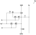
본 발명의 실시예에 의한 화소는 유기 발광 다이오드와; 제 1노드에 접속된 제 1구동전원과 상기 유기 발광 다이오드의 애노드전극 사이에 접속되며, 제 2노드의 전압에 대응하여 상기 제 1구동전원으로부터 상기 유기 발광 다이오드로 공급되는 전류량을 제어하기 위한 제 1트랜지스터와; 데이터선과 상기 제 1노드 사이에 접속되며, i(i는 자연수)번째 제 1주사선으로 제 1주사신호가 공급될 때 턴-온되는 제 2트랜지스터와; 상기 제 1트랜지스터의 제 2전극과 상기 제 2노드 사이에 접속되며, 상기 제 1주사신호가 공급될 때 턴-온되는 제 3트랜지스터와; 상기 제 1구동전원과 상기 제 2노드 사이에 접속되는 스토리지 커패시터와; 상기 제 3트랜지스터와 상기 제 2노드의 사이 또는 상기 제 1트랜지스터의 제 2전극과 상기 제 3트랜지스터의 사이에 접속되며, 상기 제 3트랜지스터가 턴-오프되는 기간 중 일부기간 동안 턴-오프 상태로 설정되는 제 1안정화 트랜지스터를 구비한다.
Description
도 2a 및 도 2b는 누설전류를 최소화하기 위한 본 발명의 실시예에 의한 트랜지스터들의 접속관계를 나타내는 도면이다.
도 3a 및 도 3b는 본 발명의 실시예에 의한 화소를 나타내는 도면이다.
도 4는 도 3a 및 도 3b에 도시된 화소의 구동방법 실시예를 나타내는 파형도이다.
도 5는 도 3a 및 도 3b의 화소가 제 2구동 주파수로 구동되는 경우의 실시예를 나타내는 도면이다.
도 6a 및 도 6b는 본 발명의 다른 실시예에 의한 화소를 나티내는 도면이다.
도 7a 및 도 7b는 본 발명의 또 다른 실시예에 의한 화소를 나타내는 도면이다.
도 8a 및 도 8b는 본 발명의 또 다른 실시예에 의한 화소를 나타내는 도면이다.
도 9a 및 도 9b는 본 발명의 또 다른 실시예에 의한 화소를 나타내는 도면이다.
도 10a 및 도 10b는 본 발명의 또 다른 실시예에 의한 화소를 나타내는 도면이다.
도 11a 내지 도 11d는 본 발명의 또 다른 실시예에 의한 화소를 나타내는 도면이다.
도 12a 및 도 12b는 본 발명의 또 다른 실시예에 의한 화소를 나타내는 도면이다.
도 13은 도 12a 및 도 12b에 도시된 화소의 구동방법 실시예를 나타내는 파형도이다.
도 14a 및 도 14b는 본 발명의 또 다른 실시예에 의한 화소를 나타내는 도면이다.
도 15a 및 도 15b는 본 발명의 또 다른 실시예에 의한 화소를 나타내는 도면이다.
도 16은 도 15a 및 도 15b에 도시된 화소의 구동방법 실시예를 나타내는 파형도이다.
도 17a 및 도 17b는 본 발명의 또 다른 실시예에 의한 화소를 나타내는 도면이다.
도 18a 및 도 18b는 본 발명의 또 다른 실시예에 의한 화소를 나타내는 도면이다.
도 19a 및 도 19b는 본 발명의 또 다른 실시예에 의한 화소를 나타내는 도면이다.
도 20a 내지 도 20d는 본 발명의 또 다른 실시예에 의한 화소를 나타내는 도면이다.
도 21a 및 도 21b는 본 발명의 또 다른 실시예에 의한 화소를 나타내는 도면이다.
도 22는 도 21a 및 도 21b에 도시된 화소의 구동방법 실시예를 나타내는 파형도이다.
도 23a 및 도 23b는 본 발명의 또 다른 실시예에 의한 화소를 나타내는 도면이다.
도 24a 및 도 24b는 본 발명의 또 다른 실시예에 의한 화소를 나타내는 도면이다.
도 25a 및 도 25b는 본 발명의 또 다른 실시예에 의한 화소를 나타내는 도면이다.
도 26a 내지 도 26d는 본 발명의 또 다른 실시예에 의한 화소를 나타내는 도면이다.
120 : 데이터 구동부 130 : 발광 구동부
140 : 타이밍 제어부 150 : 호스트 시스템
2001,2002,2003,2004,2005,2006,2007,2008 : 화소회로
Claims (57)
- 유기 발광 다이오드와;
제 1노드에 접속된 제 1구동전원과 상기 유기 발광 다이오드의 애노드전극 사이에 접속되며, 제 2노드의 전압에 대응하여 상기 제 1구동전원으로부터 상기 유기 발광 다이오드로 공급되는 전류량을 제어하기 위한 제 1트랜지스터와;
데이터선과 상기 제 1노드 사이에 접속되며, i(i는 자연수)번째 제 1주사선으로 제 1주사신호가 공급될 때 턴-온되는 제 2트랜지스터와;
상기 제 1트랜지스터의 제 2전극과 상기 제 2노드 사이에 접속되며, 상기 제 1주사신호가 공급될 때 턴-온되는 제 3트랜지스터와;
상기 제 1구동전원과 상기 제 2노드 사이에 접속되는 스토리지 커패시터와;
상기 제 3트랜지스터와 상기 제 2노드의 사이 또는 상기 제 1트랜지스터의 제 2전극과 상기 제 3트랜지스터의 사이에 접속되며, 상기 제 3트랜지스터가 턴-오프되는 기간 중 일부기간 동안 턴-오프 상태로 설정되는 제 1안정화 트랜지스터를 구비하고,
상기 제 1안정화 트랜지스터의 게이트전극은 제어전원에 접속되며,
상기 제어전원은 화소가 제 1구동 주파수로 구동되는 기간 동안 게이트 온 전압으로 설정되고, 상기 제 1구동 주파수보다 낮은 제 2구동 주파수로 구동되는 기간 중 일부기간 동안 게이트 오프 전압으로 설정되는 것을 특징으로 하는 화소. - 제 1항에 있어서,
상기 제 1트랜지스터, 상기 제 2트랜지스터 및 상기 제 3트랜지스터는 P타입의 폴리 실리콘 반도체 트랜지스터로 설정되는 것을 특징으로 하는 화소. - 제 1항에 있어서,
상기 제 1안정화 트랜지스터는 N타입의 산화물 반도체 트랜지스터로 설정되는 것을 특징으로 하는 화소. - 삭제
- 제 1항에 있어서,
상기 화소가 상기 제 2구동 주파수로 구동될 때 상기 제어전원은 상기 스토리지 커패시터에 데이터신호의 전압이 저장된 후 상기 게이트 오프 전압으로 설정되는 것을 특징으로 하는 화소. - 제 1항에 있어서,
상기 제 1노드와 상기 제 1구동전원 사이에 접속되며, i번째 발광 제어선으로 발광 제어신호가 공급될 때 턴-오프되고 그 외의 경우에 턴-온되는 제 6트랜지스터와;
상기 제 1트랜지스터의 제 2전극과 상기 유기 발광 다이오드의 애노드전극 사이에 접속되며, 상기 제 6트랜지스터와 동시에 턴-온 및 턴-오프되는 제 7트랜지스터를 더 구비하며;
상기 i번째 발광 제어선으로 공급되는 발광 제어신호는 상기 제 1주사신호보다 넓은 폭으로 설정됨과 동시에 상기 제 1주사신호와 중첩되게 공급되는 것을 특징으로 하는 화소. - 삭제
- 제 1항에 있어서,
상기 제 2노드와 제 1전원 사이에 접속되며, i번째 제 2주사선으로 제 2주사신호가 공급될 때 턴-온되는 제 4트랜지스터와;
상기 제 2노드와 상기 제 4트랜지스터의 사이 또는 상기 제 4트랜지스터와 상기 제 1전원 사이에 접속되며, 상기 제 4트랜지스터가 턴-오프되는 기간 중 일부기간 동안 턴-오프 상태로 설정되는 제 2안정화 트랜지스터를 더 구비하는 것을 특징으로 하는 화소. - 제 8항에 있어서,
상기 제 1전원은 상기 데이터선으로 공급되는 데이터신호보다 낮은 전압으로 설정되는 것을 특징으로 하는 화소. - 제 8항에 있어서,
상기 제 2안정화 트랜지스터는 N타입의 산화물 반도체 트랜지스터로 설정되는 것을 특징으로 하는 화소. - 제 8항에 있어서,
상기 제 2안정화 트랜지스터의 게이트전극은 제어전원에 접속되며,
상기 제어전원은 상기 화소가 제 1구동 주파수로 구동되는 기간 동안 게이트 온 전압으로 설정되고, 상기 제 1구동 주파수보다 낮은 제 2구동 주파수로 구동되는 기간 중 일부기간 동안 게이트 오프 전압으로 설정되는 것을 특징으로 하는 화소. - 제 11항에 있어서,
상기 화소가 상기 제 2구동 주파수로 구동될 때 상기 제어전원은 상기 스토리지 커패시터에 데이터신호의 전압이 저장된 후 상기 게이트 오프 전압으로 설정되는 것을 특징으로 하는 화소. - 제 8항에 있어서,
상기 제 1노드와 상기 제 1구동전원 사이에 접속되며, i번째 발광 제어선으로 발광 제어신호가 공급될 때 턴-오프되고 그 외의 경우에 턴-온되는 제 6트랜지스터와;
상기 제 1트랜지스터의 제 2전극과 상기 유기 발광 다이오드의 애노드전극 사이에 접속되며, 상기 제 6트랜지스터와 동시에 턴-온 및 턴-오프되는 제 7트랜지스터를 더 구비하며;
상기 i번째 발광 제어선으로 공급되는 발광 제어신호는 상기 제 1주사신호보다 넓은 폭으로 설정됨과 동시에 상기 제 1주사신호와 중첩되게 공급되는 것을 특징으로 하는 화소. - 제 13항에 있어서,
상기 제 2안정화 트랜지스터의 게이트전극은 상기 i번째 발광 제어선에 접속되는 것을 특징으로 하는 화소. - 제 8항에 있어서,
상기 i번째 제 2주사선은 i-1번째 제 1주사선으로 설정되는 것을 특징으로 하는 화소. - 제 1항에 있어서,
상기 유기 발광 다이오드의 애노드전극과 제 1전원 사이에 접속되며, i번째 제 3주사선으로 제 3주사신호가 공급될 때 턴-온되는 제 5트랜지스터와;
상기 유기 발광 다이오드의 애노드전극과 상기 제 5트랜지스터의 사이 또는 상기 제 5트랜지스터와 상기 제 1전원 사이에 접속되며, 상기 제 5트랜지스터가 턴-오프되는 기간 중 일부기간 동안 턴-오프 상태로 설정되는 제 3안정화 트랜지스터를 더 구비하는 것을 특징으로 하는 화소. - 제 16항에 있어서,
상기 제 3안정화 트랜지스터는 N타입의 산화물 반도체 트랜지스터로 설정되는 것을 특징으로 하는 화소. - 제 16항에 있어서,
상기 제 3안정화 트랜지스터의 게이트전극은 제어전원에 접속되며,
상기 제어전원은 상기 화소가 제 1구동 주파수로 구동되는 기간 동안 게이트 온 전압으로 설정되고, 상기 제 1구동 주파수보다 낮은 제 2구동 주파수로 구동되는 기간 중 일부기간 동안 게이트 오프 전압으로 설정되는 것을 특징으로 하는 화소. - 제 18항에 있어서,
상기 화소가 상기 제 2구동 주파수로 구동될 때 상기 제어전원은 상기 스토리지 커패시터에 데이터신호의 전압이 저장된 후 상기 게이트 오프 전압으로 설정되는 것을 특징으로 하는 화소. - 제 16항에 있어서,
상기 제 1노드와 상기 제 1구동전원 사이에 접속되며, i번째 발광 제어선으로 발광 제어신호가 공급될 때 턴-오프되고 그 외의 경우에 턴-온되는 제 6트랜지스터와;
상기 제 1트랜지스터의 제 2전극과 상기 유기 발광 다이오드의 애노드전극 사이에 접속되며, 상기 제 6트랜지스터와 동시에 턴-온 및 턴-오프되는 제 7트랜지스터를 더 구비하며;
상기 i번째 발광 제어선으로 공급되는 발광 제어신호는 상기 제 1주사신호보다 넓은 폭으로 설정됨과 동시에 상기 제 1주사신호와 중첩되게 공급되는 것을 특징으로 하는 화소. - 제 20항에 있어서,
상기 제 3안정화 트랜지스터의 게이트전극은 상기 i번째 발광 제어선에 접속되는 것을 특징으로 하는 화소. - 제 16항에 있어서,
상기 i번째 제 3주사선은 상기 i번째 제 1주사선으로 설정되는 것을 특징으로 하는 화소. - 유기 발광 다이오드와;
제 11노드의 전압에 대응하여 제 1구동전원으로부터 상기 유기 발광 다이오드를 경유하여 제 2구동전원으로 흐르는 전류량을 제어하기 위한 제 11트랜지스터와;
데이터선과 상기 제 11노드 사이에 접속되며, 주사선으로 주사신호가 공급될 때 턴-온되는 제 12트랜지스터와;
상기 제 11노드와 상기 제 11트랜지스터의 제 2전극 사이에 접속되는 스토리지 커패시터와;
상기 데이터선과 상기 제 12트랜지스터의 사이 또는 상기 제 12트랜지스터와 상기 제 11노드 사이에 접속되는 제 4안정화 트랜지스터를 구비하며;
상기 제 11트랜지스터 및 제 12트랜지스터는 N타입 폴리 실리콘 반도체 트랜지스터로 설정되고, 상기 제 4안정화 트랜지스터는 N타입 산화물 반도체 트랜지스터로 설정되고,
상기 제 4안정화 트랜지스터의 게이트전극은 제어전원에 접속되며,
상기 제어전원은 화소가 제 1구동 주파수로 구동되는 기간 동안 게이트 온 전압으로 설정되고, 상기 제 1구동 주파수보다 낮은 제 2구동 주파수로 구동되는 기간 중 일부기간 동안 게이트 오프 전압으로 설정되는 것을 특징으로 하는 화소. - 삭제
- 제 23항에 있어서,
상기 화소가 상기 제 2구동 주파수로 구동될 때 상기 제어전원은 상기 스토리지 커패시터에 데이터신호의 전압이 저장된 후 상기 게이트 오프 전압으로 설정되는 것을 특징으로 하는 화소. - 삭제
- 제 23항에 있어서,
상기 제 1구동전원과 상기 제 11트랜지스터의 제 1전극 사이에 접속되며, 상기 제 12트랜지스터와 턴-온 기간이 중첩되지 않는 제 13트랜지스터를 더 구비하는 것을 특징으로 하는 화소. - 유기 발광 다이오드와;
제 21노드의 전압에 대응하여 제 1구동전원으로부터 상기 유기 발광 다이오드를 경유하여 제 2구동전원으로 흐르는 전류량을 제어하기 위한 제 21트랜지스터와;
데이터선과 제 22노드 사이에 접속되며, 주사선으로 주사신호가 공급될 때 턴-온되는 제 22트랜지스터와;
상기 제 22노드와 상기 제 21트랜지스터의 제 2전극 사이에 접속되며, i-1번째 발광 제어선으로 발광 제어신호가 공급될 때 턴-오프되는 제 23트랜지스터와;
상기 제 21노드와 상기 제 21트랜지스터의 제 1전극 사이에 접속되며, 상기 주사신호가 공급될 때 턴-온되는 제 24트랜지스터와;
상기 제 21노드와 상기 제 22노드 사이에 접속되는 스토리지 커패시터와;
상기 제 21노드와 상기 제 24트랜지스터의 사이 또는 상기 제 24트랜지스터와 상기 제 21트랜지스터의 제 1전극 사이에 접속되는 제 5안정화 트랜지스터를 구비하며;
상기 제 21트랜지스터 내지 제 24트랜지스터는 N타입 폴리 실리콘 반도체 트랜지스터로 설정되고, 상기 제 5안정화 트랜지스터는 N타입 산화물 반도체 트랜지스터로 설정되고,
상기 제 5안정화 트랜지스터의 게이트전극은 제어전원에 접속되며,
상기 제어전원은 화소가 제 1구동 주파수로 구동되는 기간 동안 게이트 온 전압으로 설정되고, 상기 제 1구동 주파수보다 낮은 제 2구동 주파수로 구동되는 기간 중 일부기간 동안 게이트 오프 전압으로 설정되는 것을 특징으로 하는 화소. - 삭제
- 제 28항에 있어서,
상기 화소가 상기 제 2구동 주파수로 구동될 때 상기 제어전원은 상기 스토리지 커패시터에 데이터신호의 전압이 저장된 후 상기 게이트 오프 전압으로 설정되는 것을 특징으로 하는 화소. - 삭제
- 제 28항에 있어서,
상기 데이터선과 상기 제 22트랜지스터의 사이 또는 상기 제 22트랜지스터와 상기 제 22노드 사이에 접속되는 제 6안정화 트랜지스터를 더 구비하는 것을 특징으로 하는 화소. - 제 32항에 있어서,
상기 제 6안정화 트랜지스터는 N타입 산화물 반도체 트랜지스터로 설정되는 것을 특징으로 하는 화소. - 제 32항에 있어서,
상기 제 6안정화 트랜지스터의 게이트전극은 제어전원에 접속되며,
상기 제어전원은 상기 화소가 제 1구동 주파수로 구동되는 기간 동안 게이트 온 전압으로 설정되고, 상기 제 1구동 주파수보다 낮은 제 2구동 주파수로 구동되는 기간 중 일부기간 동안 게이트 오프 전압으로 설정되는 것을 특징으로 하는 화소. - 제 34항에 있어서,
상기 화소가 상기 제 2구동 주파수로 구동될 때 상기 제어전원은 상기 스토리지 커패시터에 데이터신호의 전압이 저장된 후 상기 게이트 오프 전압으로 설정되는 것을 특징으로 하는 화소. - 제 32항에 있어서,
상기 제 6안정화 트랜지스터의 게이트전극은 상기 주사선에 접속되는 것을 특징으로 하는 화소. - 제 28항에 있어서,
제 1전원과 상기 유기 발광 다이오드의 애노드전극 사이에 접속되며, 게이트전극이 상기 주사선에 접속되는 제 25트랜지스터와;
상기 제 1구동전원과 상기 제 21트랜지스터의 제 1전극 사이에 접속되며, 게이트전극이 i번째 발광 제어선에 접속되는 제 26트랜지스터를 더 구비하는 것을 특징으로 하는 화소. - 유기 발광 다이오드와;
제 31노드의 전압에 대응하여 제 1구동전원으로부터 상기 유기 발광 다이오드를 경유하여 제 2구동전원으로 흐르는 전류량을 제어하기 위한 제 31트랜지스터와;
제 1전원과 상기 유기 발광 다이오드의 애노드전극 사이에 접속되며, 제 2주사선으로 제 2주사신호가 공급될 때 턴-온되는 제 32트랜지스터와;
상기 제 31노드와 상기 제 31트랜지스터의 제 2전극 사이에 접속되며, 제 1주사선으로 제 1주사신호가 공급될 때 턴-온되는 제 33트랜지스터와;
상기 제 1전원과 상기 제 31노드 사이에 접속되는 스토리지 커패시터와;
상기 제 31노드와 상기 제 33트랜지스터의 사이 또는 상기 제 33트랜지스터와 상기 제 31트랜지스터의 제 2전극 사이에 접속되는 제 7안정화 트랜지스터 구비하며;
상기 제 31트랜지스터 내지 제 33트랜지스터는 N타입 폴리 실리콘 반도체 트랜지스터로 설정되고, 상기 제 7안정화 트랜지스터는 N타입 산화물 반도체 트랜지스터로 설정되고,
상기 제 7안정화 트랜지스터의 게이트전극은 제어전원에 접속되며,
상기 제어전원은 화소가 제 1구동 주파수로 구동되는 기간 동안 게이트 온 전압으로 설정되고, 상기 제 1구동 주파수보다 낮은 제 2구동 주파수로 구동되는 기간 중 일부기간 동안 게이트 오프 전압으로 설정되는 것을 특징으로 하는 화소. - 삭제
- 제 38항에 있어서,
상기 화소가 상기 제 2구동 주파수로 구동될 때 상기 제어전원은 상기 스토리지 커패시터에 데이터신호의 전압이 저장된 후 상기 게이트 오프 전압으로 설정되는 것을 특징으로 하는 화소. - 삭제
- 제 38항에 있어서,
상기 제 32트랜지스터와 상기 유기 발광 다이오드의 애노드전극 사이 또는 상기 제 1전원과 상기 제 32트랜지스터의 사이에 접속되는 제 8안정화 트랜지스터를 더 구비하는 것을 특징으로 하는 화소. - 제 42항에 있어서,
상기 제 8안정화 트랜지스터는 N타입 산화물 반도체 트랜지스터로 설정되는 것을 특징으로 하는 화소. - 제 42항에 있어서,
상기 제 8안정화 트랜지스터의 게이트전극은 제어전원에 접속되며,
상기 제어전원은 상기 화소가 제 1구동 주파수로 구동되는 기간 동안 게이트 온 전압으로 설정되고, 상기 제 1구동 주파수보다 낮은 제 2구동 주파수로 구동되는 기간 중 일부기간 동안 게이트 오프 전압으로 설정되는 것을 특징으로 하는 화소. - 제 44항에 있어서,
상기 화소가 상기 제 2구동 주파수로 구동될 때 상기 제어전원은 상기 스토리지 커패시터에 데이터신호의 전압이 저장된 후 상기 게이트 오프 전압으로 설정되는 것을 특징으로 하는 화소. - 제 42항에 있어서,
상기 제 8안정화 트랜지스터의 게이트전극은 상기 제 2주사선에 접속되는 것을 특징으로 하는 화소. - 제 38항에 있어서,
데이터선과 상기 제 31트랜지스터의 제 2전극 사이에 접속되는 제 1커패시터를 더 구비하는 것을 특징으로 하는 화소. - 삭제
- 삭제
- 삭제
- 삭제
- 삭제
- 삭제
- 삭제
- 삭제
- 삭제
- 삭제
Priority Applications (8)
| Application Number | Priority Date | Filing Date | Title |
|---|---|---|---|
| KR1020160162995A KR102547871B1 (ko) | 2016-12-01 | 2016-12-01 | 화소 및 이를 가지는 유기전계발광 표시장치 |
| US15/811,922 US10529283B2 (en) | 2016-12-01 | 2017-11-14 | Pixel including a pair of transistors in a current leakage path and organic light emitting display device having the pixel |
| CN201711193768.5A CN108133687B (zh) | 2016-12-01 | 2017-11-24 | 像素和具有该像素的有机发光显示装置 |
| US16/709,234 US11024227B2 (en) | 2016-12-01 | 2019-12-10 | Pixel and organic light emitting display device having the pixel |
| US16/709,256 US10957253B2 (en) | 2016-12-01 | 2019-12-10 | Pixel and organic light emitting display device having the pixel |
| US16/709,309 US11017720B2 (en) | 2016-12-01 | 2019-12-10 | Pixel and organic light emitting display device having the pixel |
| US17/318,564 US11769451B2 (en) | 2016-12-01 | 2021-05-12 | Pixel and organic light emitting display device having the pixel |
| US18/473,549 US12217686B2 (en) | 2016-12-01 | 2023-09-25 | Pixel and organic light emitting display device having the pixel |
Applications Claiming Priority (1)
| Application Number | Priority Date | Filing Date | Title |
|---|---|---|---|
| KR1020160162995A KR102547871B1 (ko) | 2016-12-01 | 2016-12-01 | 화소 및 이를 가지는 유기전계발광 표시장치 |
Publications (2)
| Publication Number | Publication Date |
|---|---|
| KR20180063425A KR20180063425A (ko) | 2018-06-12 |
| KR102547871B1 true KR102547871B1 (ko) | 2023-06-28 |
Family
ID=62243345
Family Applications (1)
| Application Number | Title | Priority Date | Filing Date |
|---|---|---|---|
| KR1020160162995A Active KR102547871B1 (ko) | 2016-12-01 | 2016-12-01 | 화소 및 이를 가지는 유기전계발광 표시장치 |
Country Status (3)
| Country | Link |
|---|---|
| US (6) | US10529283B2 (ko) |
| KR (1) | KR102547871B1 (ko) |
| CN (1) | CN108133687B (ko) |
Families Citing this family (28)
| Publication number | Priority date | Publication date | Assignee | Title |
|---|---|---|---|---|
| CN106710529B (zh) * | 2016-12-19 | 2019-02-05 | 上海天马有机发光显示技术有限公司 | 一种像素驱动电路、驱动方法及有机发光显示面板 |
| KR102555397B1 (ko) * | 2018-06-15 | 2023-07-14 | 삼성디스플레이 주식회사 | 화소 및 이를 포함하는 표시 장치 |
| KR102527847B1 (ko) * | 2018-06-18 | 2023-05-03 | 삼성디스플레이 주식회사 | 표시 장치 |
| US11164518B2 (en) * | 2018-06-19 | 2021-11-02 | Samsung Display Co., Ltd. | Display device |
| KR102544572B1 (ko) | 2018-07-18 | 2023-06-19 | 삼성디스플레이 주식회사 | 표시 장치 |
| KR102593537B1 (ko) * | 2018-12-27 | 2023-10-26 | 삼성디스플레이 주식회사 | 구동 컨트롤러, 그것을 포함하는 표시 장치 및 표시 장치의 구동 방법 |
| KR102646885B1 (ko) * | 2019-04-15 | 2024-03-14 | 삼성디스플레이 주식회사 | 화소 및 이를 포함하는 표시 장치 |
| CN110277060B (zh) * | 2019-05-21 | 2021-11-16 | 合肥维信诺科技有限公司 | 一种像素电路和显示装置 |
| KR102656092B1 (ko) | 2019-07-15 | 2024-04-11 | 삼성디스플레이 주식회사 | 표시 장치 및 이의 제조 방법 |
| KR102731318B1 (ko) * | 2019-08-16 | 2024-11-19 | 삼성디스플레이 주식회사 | 화소 회로 |
| KR102599715B1 (ko) | 2019-08-21 | 2023-11-09 | 삼성디스플레이 주식회사 | 화소 회로 |
| KR102710739B1 (ko) * | 2019-10-25 | 2024-09-30 | 삼성디스플레이 주식회사 | 화소 및 이를 포함하는 표시 장치 |
| CN112967653B (zh) * | 2019-12-11 | 2024-05-31 | 厦门天马微电子有限公司 | 一种显示面板及显示装置 |
| CN111179841B (zh) * | 2020-02-28 | 2021-05-11 | 京东方科技集团股份有限公司 | 像素补偿电路及其驱动方法、显示装置 |
| KR102756484B1 (ko) * | 2020-05-29 | 2025-01-21 | 삼성디스플레이 주식회사 | 표시 장치 |
| CN117542318A (zh) * | 2020-07-15 | 2024-02-09 | 武汉华星光电半导体显示技术有限公司 | 像素电路及其驱动方法、显示装置 |
| CN111816118B (zh) * | 2020-08-28 | 2020-12-15 | 京东方科技集团股份有限公司 | 显示面板及显示装置 |
| CN112053661B (zh) * | 2020-09-28 | 2023-04-11 | 京东方科技集团股份有限公司 | 像素电路、像素驱动方法、显示面板和显示装置 |
| KR102808219B1 (ko) | 2020-11-20 | 2025-05-15 | 삼성디스플레이 주식회사 | 표시 장치 |
| CN112599097A (zh) * | 2021-01-06 | 2021-04-02 | 武汉华星光电半导体显示技术有限公司 | 像素驱动电路及显示面板 |
| WO2022226727A1 (zh) * | 2021-04-26 | 2022-11-03 | 京东方科技集团股份有限公司 | 像素电路、像素驱动方法和显示装置 |
| GB2615719A (en) * | 2021-04-26 | 2023-08-16 | Boe Technology Group Co Ltd | Pixel circuit, pixel driving method and display device |
| TWI780844B (zh) * | 2021-07-29 | 2022-10-11 | 友達光電股份有限公司 | 驅動電路 |
| WO2023004813A1 (zh) | 2021-07-30 | 2023-02-02 | 京东方科技集团股份有限公司 | 像素电路、驱动方法和显示装置 |
| US12236829B2 (en) * | 2021-07-30 | 2025-02-25 | Chengdu Boe Optoelectronics Technology Co., Ltd. | Pixel driving circuit and driving method thereof, and display panel |
| CN115035858B (zh) * | 2022-06-29 | 2024-07-23 | 武汉天马微电子有限公司 | 像素电路及其驱动方法、显示面板 |
| CN115294938B (zh) * | 2022-08-03 | 2024-06-25 | 武汉天马微电子有限公司 | 一种像素扫描电路、显示面板及显示装置 |
| KR20240048592A (ko) | 2022-10-06 | 2024-04-16 | 삼성디스플레이 주식회사 | 표시 장치 |
Citations (1)
| Publication number | Priority date | Publication date | Assignee | Title |
|---|---|---|---|---|
| CN105679247A (zh) * | 2010-10-28 | 2016-06-15 | 三星显示有限公司 | 有机发光显示器 |
Family Cites Families (16)
| Publication number | Priority date | Publication date | Assignee | Title |
|---|---|---|---|---|
| CA2518276A1 (en) * | 2005-09-13 | 2007-03-13 | Ignis Innovation Inc. | Compensation technique for luminance degradation in electro-luminance devices |
| KR101048965B1 (ko) | 2009-01-22 | 2011-07-12 | 삼성모바일디스플레이주식회사 | 유기 전계발광 표시장치 |
| CN102346999B (zh) * | 2011-06-27 | 2013-11-06 | 昆山工研院新型平板显示技术中心有限公司 | Amoled像素电路及其驱动方法 |
| KR20140028921A (ko) * | 2012-08-31 | 2014-03-10 | 삼성디스플레이 주식회사 | 화소 및 이를 이용한 유기전계발광 표시장치 |
| KR101985298B1 (ko) * | 2012-10-26 | 2019-06-04 | 삼성디스플레이 주식회사 | 유기 발광 표시 장치 및 그 제조 방법 |
| JP2014109707A (ja) * | 2012-12-03 | 2014-06-12 | Samsung Display Co Ltd | 電気光学装置の駆動方法および電気光学装置 |
| KR20140081262A (ko) * | 2012-12-21 | 2014-07-01 | 삼성디스플레이 주식회사 | 화소 및 이를 이용한 유기전계발광 표시장치 |
| KR20140096862A (ko) * | 2013-01-29 | 2014-08-06 | 삼성디스플레이 주식회사 | 화소, 이를 포함하는 유기 전계 발광 표시 장치 및 이의 구동 방법 |
| US9490276B2 (en) * | 2014-02-25 | 2016-11-08 | Lg Display Co., Ltd. | Display backplane and method of fabricating the same |
| CN104167168B (zh) | 2014-06-23 | 2016-09-07 | 京东方科技集团股份有限公司 | 像素电路及其驱动方法和显示装置 |
| CN105448235B (zh) | 2014-09-28 | 2018-01-26 | 昆山工研院新型平板显示技术中心有限公司 | Amoled像素单元及其驱动方法、amoled显示装置 |
| EP3098804A3 (en) | 2015-05-28 | 2016-12-21 | LG Display Co., Ltd. | Organic light emitting display |
| EP3098805B1 (en) | 2015-05-28 | 2018-07-25 | LG Display Co., Ltd. | Organic light emitting display and circuit thereof |
| US10121430B2 (en) * | 2015-11-16 | 2018-11-06 | Apple Inc. | Displays with series-connected switching transistors |
| US9818344B2 (en) * | 2015-12-04 | 2017-11-14 | Apple Inc. | Display with light-emitting diodes |
| KR102730406B1 (ko) * | 2016-12-12 | 2024-11-18 | 삼성디스플레이 주식회사 | 화소 및 이를 가지는 유기전계발광 표시장치 |
-
2016
- 2016-12-01 KR KR1020160162995A patent/KR102547871B1/ko active Active
-
2017
- 2017-11-14 US US15/811,922 patent/US10529283B2/en active Active
- 2017-11-24 CN CN201711193768.5A patent/CN108133687B/zh active Active
-
2019
- 2019-12-10 US US16/709,309 patent/US11017720B2/en active Active
- 2019-12-10 US US16/709,256 patent/US10957253B2/en active Active
- 2019-12-10 US US16/709,234 patent/US11024227B2/en active Active
-
2021
- 2021-05-12 US US17/318,564 patent/US11769451B2/en active Active
-
2023
- 2023-09-25 US US18/473,549 patent/US12217686B2/en active Active
Patent Citations (1)
| Publication number | Priority date | Publication date | Assignee | Title |
|---|---|---|---|---|
| CN105679247A (zh) * | 2010-10-28 | 2016-06-15 | 三星显示有限公司 | 有机发光显示器 |
Also Published As
| Publication number | Publication date |
|---|---|
| CN108133687A (zh) | 2018-06-08 |
| US20200118491A1 (en) | 2020-04-16 |
| US20200111416A1 (en) | 2020-04-09 |
| US11769451B2 (en) | 2023-09-26 |
| US10957253B2 (en) | 2021-03-23 |
| US11024227B2 (en) | 2021-06-01 |
| US20240013722A1 (en) | 2024-01-11 |
| US12217686B2 (en) | 2025-02-04 |
| US11017720B2 (en) | 2021-05-25 |
| US20180158407A1 (en) | 2018-06-07 |
| US10529283B2 (en) | 2020-01-07 |
| CN108133687B (zh) | 2022-07-12 |
| US20210264856A1 (en) | 2021-08-26 |
| US20200111415A1 (en) | 2020-04-09 |
| KR20180063425A (ko) | 2018-06-12 |
Similar Documents
| Publication | Publication Date | Title |
|---|---|---|
| KR102547871B1 (ko) | 화소 및 이를 가지는 유기전계발광 표시장치 | |
| KR102729321B1 (ko) | 화소 및 스테이지 회로와 이를 가지는 유기전계발광 표시장치 | |
| US11688342B2 (en) | Pixel and organic light emitting display device having the pixel | |
| KR102818266B1 (ko) | 화소 및 스테이지 회로와 이를 가지는 유기전계발광 표시장치 | |
| KR102730406B1 (ko) | 화소 및 이를 가지는 유기전계발광 표시장치 | |
| CN114582288A (zh) | 有机发光显示设备 | |
| US10692440B2 (en) | Pixel and organic light emitting display device including the same | |
| KR101142660B1 (ko) | 화소 및 이를 이용한 유기전계발광 표시장치 | |
| KR102583838B1 (ko) | 화소 및 이를 이용한 유기전계발광 표시장치 | |
| KR20190040849A (ko) | 유기 발광 표시 장치 및 그의 구동 방법 | |
| CN114743503B (zh) | 像素 |
Legal Events
| Date | Code | Title | Description |
|---|---|---|---|
| PA0109 | Patent application |
Patent event code: PA01091R01D Comment text: Patent Application Patent event date: 20161201 |
|
| PG1501 | Laying open of application | ||
| PA0201 | Request for examination |
Patent event code: PA02012R01D Patent event date: 20211022 Comment text: Request for Examination of Application Patent event code: PA02011R01I Patent event date: 20161201 Comment text: Patent Application |
|
| E902 | Notification of reason for refusal | ||
| PE0902 | Notice of grounds for rejection |
Comment text: Notification of reason for refusal Patent event date: 20221027 Patent event code: PE09021S01D |
|
| E701 | Decision to grant or registration of patent right | ||
| PE0701 | Decision of registration |
Patent event code: PE07011S01D Comment text: Decision to Grant Registration Patent event date: 20230322 |
|
| PG1601 | Publication of registration |