KR102545322B1 - 유기 발광 소자를 이용한 조명 장치 - Google Patents
유기 발광 소자를 이용한 조명 장치 Download PDFInfo
- Publication number
- KR102545322B1 KR102545322B1 KR1020180086402A KR20180086402A KR102545322B1 KR 102545322 B1 KR102545322 B1 KR 102545322B1 KR 1020180086402 A KR1020180086402 A KR 1020180086402A KR 20180086402 A KR20180086402 A KR 20180086402A KR 102545322 B1 KR102545322 B1 KR 102545322B1
- Authority
- KR
- South Korea
- Prior art keywords
- electrode
- layer
- light emitting
- disposed
- organic light
- Prior art date
- Legal status (The legal status is an assumption and is not a legal conclusion. Google has not performed a legal analysis and makes no representation as to the accuracy of the status listed.)
- Active
Links
Images


Classifications
-
- H—ELECTRICITY
- H10—SEMICONDUCTOR DEVICES; ELECTRIC SOLID-STATE DEVICES NOT OTHERWISE PROVIDED FOR
- H10K—ORGANIC ELECTRIC SOLID-STATE DEVICES
- H10K50/00—Organic light-emitting devices
- H10K50/80—Constructional details
- H10K50/805—Electrodes
-
- H—ELECTRICITY
- H10—SEMICONDUCTOR DEVICES; ELECTRIC SOLID-STATE DEVICES NOT OTHERWISE PROVIDED FOR
- H10K—ORGANIC ELECTRIC SOLID-STATE DEVICES
- H10K50/00—Organic light-emitting devices
- H10K50/10—OLEDs or polymer light-emitting diodes [PLED]
- H10K50/11—OLEDs or polymer light-emitting diodes [PLED] characterised by the electroluminescent [EL] layers
- H10K50/125—OLEDs or polymer light-emitting diodes [PLED] characterised by the electroluminescent [EL] layers specially adapted for multicolour light emission, e.g. for emitting white light
- H10K50/13—OLEDs or polymer light-emitting diodes [PLED] characterised by the electroluminescent [EL] layers specially adapted for multicolour light emission, e.g. for emitting white light comprising stacked EL layers within one EL unit
-
- H—ELECTRICITY
- H10—SEMICONDUCTOR DEVICES; ELECTRIC SOLID-STATE DEVICES NOT OTHERWISE PROVIDED FOR
- H10K—ORGANIC ELECTRIC SOLID-STATE DEVICES
- H10K50/00—Organic light-emitting devices
- H10K50/80—Constructional details
- H10K50/805—Electrodes
- H10K50/81—Anodes
- H10K50/818—Reflective anodes, e.g. ITO combined with thick metallic layers
-
- H—ELECTRICITY
- H10—SEMICONDUCTOR DEVICES; ELECTRIC SOLID-STATE DEVICES NOT OTHERWISE PROVIDED FOR
- H10K—ORGANIC ELECTRIC SOLID-STATE DEVICES
- H10K50/00—Organic light-emitting devices
- H10K50/80—Constructional details
- H10K50/805—Electrodes
- H10K50/82—Cathodes
- H10K50/824—Cathodes combined with auxiliary electrodes
-
- H—ELECTRICITY
- H10—SEMICONDUCTOR DEVICES; ELECTRIC SOLID-STATE DEVICES NOT OTHERWISE PROVIDED FOR
- H10K—ORGANIC ELECTRIC SOLID-STATE DEVICES
- H10K50/00—Organic light-emitting devices
- H10K50/80—Constructional details
- H10K50/805—Electrodes
- H10K50/82—Cathodes
- H10K50/828—Transparent cathodes, e.g. comprising thin metal layers
-
- H—ELECTRICITY
- H10—SEMICONDUCTOR DEVICES; ELECTRIC SOLID-STATE DEVICES NOT OTHERWISE PROVIDED FOR
- H10K—ORGANIC ELECTRIC SOLID-STATE DEVICES
- H10K50/00—Organic light-emitting devices
- H10K50/80—Constructional details
- H10K50/85—Arrangements for extracting light from the devices
- H10K50/854—Arrangements for extracting light from the devices comprising scattering means
-
- H—ELECTRICITY
- H10—SEMICONDUCTOR DEVICES; ELECTRIC SOLID-STATE DEVICES NOT OTHERWISE PROVIDED FOR
- H10K—ORGANIC ELECTRIC SOLID-STATE DEVICES
- H10K50/00—Organic light-emitting devices
- H10K50/80—Constructional details
- H10K50/85—Arrangements for extracting light from the devices
- H10K50/858—Arrangements for extracting light from the devices comprising refractive means, e.g. lenses
-
- F—MECHANICAL ENGINEERING; LIGHTING; HEATING; WEAPONS; BLASTING
- F21—LIGHTING
- F21Y—INDEXING SCHEME ASSOCIATED WITH SUBCLASSES F21K, F21L, F21S and F21V, RELATING TO THE FORM OR THE KIND OF THE LIGHT SOURCES OR OF THE COLOUR OF THE LIGHT EMITTED
- F21Y2115/00—Light-generating elements of semiconductor light sources
- F21Y2115/10—Light-emitting diodes [LED]
- F21Y2115/15—Organic light-emitting diodes [OLED]
-
- H01L2251/5361—
-
- H—ELECTRICITY
- H10—SEMICONDUCTOR DEVICES; ELECTRIC SOLID-STATE DEVICES NOT OTHERWISE PROVIDED FOR
- H10K—ORGANIC ELECTRIC SOLID-STATE DEVICES
- H10K2102/00—Constructional details relating to the organic devices covered by this subclass
- H10K2102/301—Details of OLEDs
- H10K2102/341—Short-circuit prevention
-
- H—ELECTRICITY
- H10—SEMICONDUCTOR DEVICES; ELECTRIC SOLID-STATE DEVICES NOT OTHERWISE PROVIDED FOR
- H10K—ORGANIC ELECTRIC SOLID-STATE DEVICES
- H10K50/00—Organic light-emitting devices
- H10K50/80—Constructional details
- H10K50/805—Electrodes
- H10K50/81—Anodes
- H10K50/814—Anodes combined with auxiliary electrodes, e.g. ITO layer combined with metal lines
-
- H—ELECTRICITY
- H10—SEMICONDUCTOR DEVICES; ELECTRIC SOLID-STATE DEVICES NOT OTHERWISE PROVIDED FOR
- H10K—ORGANIC ELECTRIC SOLID-STATE DEVICES
- H10K50/00—Organic light-emitting devices
- H10K50/80—Constructional details
- H10K50/805—Electrodes
- H10K50/81—Anodes
- H10K50/816—Multilayers, e.g. transparent multilayers
-
- H—ELECTRICITY
- H10—SEMICONDUCTOR DEVICES; ELECTRIC SOLID-STATE DEVICES NOT OTHERWISE PROVIDED FOR
- H10K—ORGANIC ELECTRIC SOLID-STATE DEVICES
- H10K50/00—Organic light-emitting devices
- H10K50/80—Constructional details
- H10K50/84—Passivation; Containers; Encapsulations
- H10K50/842—Containers
- H10K50/8423—Metallic sealing arrangements
-
- H—ELECTRICITY
- H10—SEMICONDUCTOR DEVICES; ELECTRIC SOLID-STATE DEVICES NOT OTHERWISE PROVIDED FOR
- H10K—ORGANIC ELECTRIC SOLID-STATE DEVICES
- H10K59/00—Integrated devices, or assemblies of multiple devices, comprising at least one organic light-emitting element covered by group H10K50/00
- H10K59/30—Devices specially adapted for multicolour light emission
- H10K59/32—Stacked devices having two or more layers, each emitting at different wavelengths
Landscapes
- Physics & Mathematics (AREA)
- Optics & Photonics (AREA)
- Electroluminescent Light Sources (AREA)
Abstract
Description
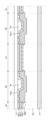
도 2는 본 발명의 일 실시예에 따른 유기 발광 소자를 이용한 조명 장치의 단면도이다.
도 3a 내지 3c은 본 발명의 일 실시예에 따른 유기층의 스택 구조를 나타내는 단면도이다.
도 4a는 본 발명의 일 실시예에 따른 유기 발광 소자를 이용하는 조명 장치의 정면도이다.
도 4b는 본 발명의 일 실시예에 따른 유기 발광 소자를 이용하는 조명 장치의 조명부를 확대하여 나타낸 도면이다.
도 5는 도 4a에 도시된 Ⅰ-Ⅰ'선 및 Ⅱ-Ⅱ'에 따른 단면도이다.
도 6a 내지 6d는 도 4b에 도시된 Ⅲ-Ⅲ'에 따른 복수의 단면도들이다.
도 7은 본 발명의 일 실시예에 따른 유기 발광 소자를 포함하는 조명 장치의 발광 경로를 나타내는 도면이다.
도 8은 본 발명의 일 실시예에 따른 유기 발광 소자를 포함하는 조명 장치의 배광 분포를 설명하기 위한 그래프이다.
도 9a는 본 발명의 일 실시예의 중간층 전극의 두께에 따른 전면 휘도의 관계를 나타내는 그래프이고, 도 9b는 본 발명의 일 실시예의 제1 전극의 반사율에 따른 전면 휘도의 관계를 나타내는 그래프이다.
도 10a는 본 발명의 일 실시예의 하층 전극의 굴절률에 따른 전면 휘도의 관계를 나타내는 그래프이고, 도 10b는 본 발명의 일 실시예의 하층 전극의 두께에 따른 전면 휘도의 관계를 나타내는 그래프이다.
110: 유기 발광 소자 유닛
120: 봉지부
130: 외부 광추출층
111: 기판
112: 내부 광추출층
113: 평탄화층
114: 배리어층
115: 제1 전극
116: 유기층
117: 제2 전극
121: 점착층
122: 금속 필름
123: 보호 필름
115a: 하층 전극
115b: 중간층 전극
115c: 상층 전극
115p: 제1 컨택 전극
117p: 제2 컨택 전극
INS: 절연층
AL: 보조 배선
EA: 조명부
Claims (12)
- 발광 영역 및 비발광 영역으로 구분되고,
제1 전극;
상기 제1 전극 상에 배치되는 유기층;
상기 유기층 상에 배치되는 제2 전극;
상기 비발광 영역에 배치되는 절연층; 및
상기 비발광 영역에 배치되는 제1 전극에 전기적으로 연결되는 보조 배선을 포함하고,
상기 발광 영역에 배치되는 제1 전극은, 적어도 하나의 금속층 및 적어도 하나의 유전체층을 포함하고,
상기 비발광 영역에 배치되는 제1 전극은 적어도 하나의 유전체층만을 포함하며,
상기 보조 배선의 상면 및 측면은 상기 비발광 영역에 배치되는 제1 전극에 의해 완전히 덮히는, 유기 발광 소자를 이용한 조명 장치. - 제1 항에 있어서,
상기 절연층은,
상기 비발광 영역에 배치되는 제1 전극에 내로우 패스(narrow path)를 구현하는 단락 방지(Short Reduction) 패턴을 포함하는, 유기 발광 소자를 이용한 조명 장치. - 제1 항에 있어서,
상기 발광 영역에 배치되는 제1 전극은,
상기 유기층과 접촉하고 유전체로 구성되는 상층 전극;
상기 상층 전극과 접촉하고 금속으로 구성되는 중간층 전극 및
상기 중간층 전극과 접촉하고 유전체로 구성되는 하층 전극을 포함하는, 유기 발광 소자를 이용한 조명 장치. - 제3 항에 있어서,
상기 비발광 영역에 배치되는 제1 전극은,
상기 상층 전극으로 구성되는, 유기 발광 소자를 이용한 조명 장치. - 제3 항에 있어서,
상기 비발광 영역에 배치되는 제1 전극은,
상기 하층 전극으로 구성되는, 유기 발광 소자를 이용한 조명 장치. - 제3 항에 있어서,
상기 비발광 영역에 배치되는 제1 전극은,
상기 상층 전극 및 상기 하층 전극을 포함하는, 유기 발광 소자를 이용한 조명 장치. - 제3 항에 있어서,
상기 상층 전극은 1000Å보다 얇은 두께의 ITO(Indium-Tin-Oxide)로 구성되는, 유기 발광 소자를 이용한 조명 장치. - 제3 항에 있어서,
상기 중간층 전극은 150Å 내지 350Å의 두께의 금속층으로 구성되는, 유기 발광 소자를 이용한 조명 장치. - 제3항에 있어서,
상기 하층 전극의 굴절률은 1.4 내지 1.5인, 유기 발광 소자를 이용한 조명 장치. - 제1항에 있어서,
상기 제1 전극의 반사율은 40% 내지 70%인, 유기 발광 소자를 이용한 조명 장치. - 삭제
- 발광 영역 및 비발광 영역으로 구분되고,
제1 전극;
상기 제1 전극 상에 배치되는 유기층;
상기 유기층 상에 배치되는 제2 전극;
상기 비발광 영역에 배치되는 절연층; 및
상기 비발광 영역에 배치되는 제1 전극에 전기적으로 연결되는 보조 배선을 포함하고,
상기 발광 영역에 배치되는 제1 전극은, 적어도 하나의 금속층 및 적어도 하나의 유전체층을 포함하고,
상기 비발광 영역에 배치되는 제1 전극은 적어도 하나의 유전체층만을 포함하며,
상기 비발광 영역에 배치되는 제1 전극은,
유전체로 구성되는 하층 전극; 및
상기 하층 전극 상에 배치되며 유전체로 구성되는 상층 전극을 포함하고,상기 보조 배선은
상기 상층 전극과 상기 하층 전극 사이에 배치되는, 유기 발광 소자를 이용한 조명 장치.
Priority Applications (3)
| Application Number | Priority Date | Filing Date | Title |
|---|---|---|---|
| KR1020180086402A KR102545322B1 (ko) | 2018-07-25 | 2018-07-25 | 유기 발광 소자를 이용한 조명 장치 |
| CN201910634374.1A CN110783475B (zh) | 2018-07-25 | 2019-07-12 | 使用有机发光二极管的照明装置 |
| US16/517,131 US11239441B2 (en) | 2018-07-25 | 2019-07-19 | Lighting apparatus using organic light emitting diode |
Applications Claiming Priority (1)
| Application Number | Priority Date | Filing Date | Title |
|---|---|---|---|
| KR1020180086402A KR102545322B1 (ko) | 2018-07-25 | 2018-07-25 | 유기 발광 소자를 이용한 조명 장치 |
Publications (2)
| Publication Number | Publication Date |
|---|---|
| KR20200011670A KR20200011670A (ko) | 2020-02-04 |
| KR102545322B1 true KR102545322B1 (ko) | 2023-06-19 |
Family
ID=69178686
Family Applications (1)
| Application Number | Title | Priority Date | Filing Date |
|---|---|---|---|
| KR1020180086402A Active KR102545322B1 (ko) | 2018-07-25 | 2018-07-25 | 유기 발광 소자를 이용한 조명 장치 |
Country Status (3)
| Country | Link |
|---|---|
| US (1) | US11239441B2 (ko) |
| KR (1) | KR102545322B1 (ko) |
| CN (1) | CN110783475B (ko) |
Citations (2)
| Publication number | Priority date | Publication date | Assignee | Title |
|---|---|---|---|---|
| US20050007015A1 (en) * | 2003-05-29 | 2005-01-13 | Seiichi Yokoyama | Method of manufacturing laminated structure, laminated structure, display device and display unit |
| US20170038872A1 (en) * | 2015-03-31 | 2017-02-09 | Boe Technology Group Co., Ltd. | Touch screen and preparation method thereof |
Family Cites Families (11)
| Publication number | Priority date | Publication date | Assignee | Title |
|---|---|---|---|---|
| JP2001223087A (ja) * | 2000-02-08 | 2001-08-17 | Sharp Corp | 電界発光素子の製造方法 |
| FI113154B (fi) * | 2001-09-19 | 2004-03-15 | Marioff Corp Oy | Palonsammutusmenetelmä ja -laitteisto |
| KR100579192B1 (ko) * | 2004-03-11 | 2006-05-11 | 삼성에스디아이 주식회사 | 전면 발광 구조를 갖는 유기 전계 발광 표시 장치 및 이의제조방법 |
| KR100683693B1 (ko) | 2004-11-10 | 2007-02-15 | 삼성에스디아이 주식회사 | 발광 장치 |
| KR100788589B1 (ko) * | 2007-01-19 | 2007-12-26 | 삼성에스디아이 주식회사 | 유기 전계 발광 표시 장치 |
| KR20120042037A (ko) * | 2010-10-22 | 2012-05-03 | 삼성모바일디스플레이주식회사 | 유기 발광 장치 및 그 제조 방법 |
| KR101480928B1 (ko) * | 2012-08-07 | 2015-01-09 | 엘지디스플레이 주식회사 | 유기전계발광표시장치 |
| JPWO2016162938A1 (ja) * | 2015-04-07 | 2017-08-31 | 株式会社野田スクリーン | 半導体装置 |
| KR102390441B1 (ko) * | 2015-10-15 | 2022-04-26 | 삼성디스플레이 주식회사 | 유기발광 표시장치 |
| KR102473101B1 (ko) * | 2016-04-04 | 2022-12-01 | 티씨엘 차이나 스타 옵토일렉트로닉스 테크놀로지 컴퍼니 리미티드 | 표시 장치 |
| KR102596065B1 (ko) * | 2016-07-04 | 2023-11-01 | 삼성디스플레이 주식회사 | 유기발광 표시장치 및 이의 제조 방법 |
-
2018
- 2018-07-25 KR KR1020180086402A patent/KR102545322B1/ko active Active
-
2019
- 2019-07-12 CN CN201910634374.1A patent/CN110783475B/zh active Active
- 2019-07-19 US US16/517,131 patent/US11239441B2/en active Active
Patent Citations (2)
| Publication number | Priority date | Publication date | Assignee | Title |
|---|---|---|---|---|
| US20050007015A1 (en) * | 2003-05-29 | 2005-01-13 | Seiichi Yokoyama | Method of manufacturing laminated structure, laminated structure, display device and display unit |
| US20170038872A1 (en) * | 2015-03-31 | 2017-02-09 | Boe Technology Group Co., Ltd. | Touch screen and preparation method thereof |
Also Published As
| Publication number | Publication date |
|---|---|
| US20200035943A1 (en) | 2020-01-30 |
| CN110783475B (zh) | 2022-06-14 |
| CN110783475A (zh) | 2020-02-11 |
| US11239441B2 (en) | 2022-02-01 |
| KR20200011670A (ko) | 2020-02-04 |
Similar Documents
| Publication | Publication Date | Title |
|---|---|---|
| KR102480881B1 (ko) | 유기 발광 소자를 이용한 조명 장치 및 이의 제조 방법 | |
| US11094908B2 (en) | Lighting apparatus using organic light emitting diode | |
| US10910586B2 (en) | Lighting apparatus using organic light emitting diode | |
| US10950817B2 (en) | Lighting apparatus using organic light emitting diode having conductive layer with high resistance on substrate | |
| US10847749B2 (en) | Lighting apparatus using organic light emitting diode | |
| KR102545322B1 (ko) | 유기 발광 소자를 이용한 조명 장치 | |
| KR102576752B1 (ko) | 유기 발광 소자를 이용한 조명 장치 | |
| KR102838585B1 (ko) | 유기 발광 소자를 이용한 조명 장치 | |
| KR102589995B1 (ko) | 유기 발광 소자를 이용한 조명 장치 | |
| KR102547989B1 (ko) | 유기 발광 소자를 이용한 조명 장치 및 이의 제조 방법 | |
| KR20200066877A (ko) | 유기 발광 소자를 이용한 조명 장치 |
Legal Events
| Date | Code | Title | Description |
|---|---|---|---|
| PA0109 | Patent application |
St.27 status event code: A-0-1-A10-A12-nap-PA0109 |
|
| PG1501 | Laying open of application |
St.27 status event code: A-1-1-Q10-Q12-nap-PG1501 |
|
| A201 | Request for examination | ||
| PA0201 | Request for examination |
St.27 status event code: A-1-2-D10-D11-exm-PA0201 |
|
| E902 | Notification of reason for refusal | ||
| PE0902 | Notice of grounds for rejection |
St.27 status event code: A-1-2-D10-D21-exm-PE0902 |
|
| T11-X000 | Administrative time limit extension requested |
St.27 status event code: U-3-3-T10-T11-oth-X000 |
|
| P22-X000 | Classification modified |
St.27 status event code: A-2-2-P10-P22-nap-X000 |
|
| P22-X000 | Classification modified |
St.27 status event code: A-2-2-P10-P22-nap-X000 |
|
| E13-X000 | Pre-grant limitation requested |
St.27 status event code: A-2-3-E10-E13-lim-X000 |
|
| P11-X000 | Amendment of application requested |
St.27 status event code: A-2-2-P10-P11-nap-X000 |
|
| P13-X000 | Application amended |
St.27 status event code: A-2-2-P10-P13-nap-X000 |
|
| E701 | Decision to grant or registration of patent right | ||
| PE0701 | Decision of registration |
St.27 status event code: A-1-2-D10-D22-exm-PE0701 |
|
| GRNT | Written decision to grant | ||
| PR0701 | Registration of establishment |
St.27 status event code: A-2-4-F10-F11-exm-PR0701 |
|
| PR1002 | Payment of registration fee |
St.27 status event code: A-2-2-U10-U11-oth-PR1002 Fee payment year number: 1 |
|
| PG1601 | Publication of registration |
St.27 status event code: A-4-4-Q10-Q13-nap-PG1601 |
|
| P22-X000 | Classification modified |
St.27 status event code: A-4-4-P10-P22-nap-X000 |