KR102307062B1 - 반도체 소자, 반도체 소자 패키지 및 조명 장치 - Google Patents
반도체 소자, 반도체 소자 패키지 및 조명 장치 Download PDFInfo
- Publication number
- KR102307062B1 KR102307062B1 KR1020140154974A KR20140154974A KR102307062B1 KR 102307062 B1 KR102307062 B1 KR 102307062B1 KR 1020140154974 A KR1020140154974 A KR 1020140154974A KR 20140154974 A KR20140154974 A KR 20140154974A KR 102307062 B1 KR102307062 B1 KR 102307062B1
- Authority
- KR
- South Korea
- Prior art keywords
- layer
- semiconductor device
- electrode
- ubm
- disposed
- Prior art date
- Legal status (The legal status is an assumption and is not a legal conclusion. Google has not performed a legal analysis and makes no representation as to the accuracy of the status listed.)
- Active
Links
Images


Classifications
-
- H—ELECTRICITY
- H10—SEMICONDUCTOR DEVICES; ELECTRIC SOLID-STATE DEVICES NOT OTHERWISE PROVIDED FOR
- H10H—INORGANIC LIGHT-EMITTING SEMICONDUCTOR DEVICES HAVING POTENTIAL BARRIERS
- H10H20/00—Individual inorganic light-emitting semiconductor devices having potential barriers, e.g. light-emitting diodes [LED]
- H10H20/80—Constructional details
- H10H20/85—Packages
- H10H20/857—Interconnections, e.g. lead-frames, bond wires or solder balls
-
- H—ELECTRICITY
- H10—SEMICONDUCTOR DEVICES; ELECTRIC SOLID-STATE DEVICES NOT OTHERWISE PROVIDED FOR
- H10H—INORGANIC LIGHT-EMITTING SEMICONDUCTOR DEVICES HAVING POTENTIAL BARRIERS
- H10H20/00—Individual inorganic light-emitting semiconductor devices having potential barriers, e.g. light-emitting diodes [LED]
- H10H20/80—Constructional details
- H10H20/81—Bodies
- H10H20/811—Bodies having quantum effect structures or superlattices, e.g. tunnel junctions
- H10H20/812—Bodies having quantum effect structures or superlattices, e.g. tunnel junctions within the light-emitting regions, e.g. having quantum confinement structures
-
- H—ELECTRICITY
- H10—SEMICONDUCTOR DEVICES; ELECTRIC SOLID-STATE DEVICES NOT OTHERWISE PROVIDED FOR
- H10H—INORGANIC LIGHT-EMITTING SEMICONDUCTOR DEVICES HAVING POTENTIAL BARRIERS
- H10H20/00—Individual inorganic light-emitting semiconductor devices having potential barriers, e.g. light-emitting diodes [LED]
- H10H20/80—Constructional details
- H10H20/81—Bodies
- H10H20/822—Materials of the light-emitting regions
- H10H20/824—Materials of the light-emitting regions comprising only Group III-V materials, e.g. GaP
- H10H20/825—Materials of the light-emitting regions comprising only Group III-V materials, e.g. GaP containing nitrogen, e.g. GaN
-
- H—ELECTRICITY
- H10—SEMICONDUCTOR DEVICES; ELECTRIC SOLID-STATE DEVICES NOT OTHERWISE PROVIDED FOR
- H10H—INORGANIC LIGHT-EMITTING SEMICONDUCTOR DEVICES HAVING POTENTIAL BARRIERS
- H10H20/00—Individual inorganic light-emitting semiconductor devices having potential barriers, e.g. light-emitting diodes [LED]
- H10H20/80—Constructional details
- H10H20/83—Electrodes
- H10H20/831—Electrodes characterised by their shape
- H10H20/8312—Electrodes characterised by their shape extending at least partially through the bodies
-
- H—ELECTRICITY
- H10—SEMICONDUCTOR DEVICES; ELECTRIC SOLID-STATE DEVICES NOT OTHERWISE PROVIDED FOR
- H10H—INORGANIC LIGHT-EMITTING SEMICONDUCTOR DEVICES HAVING POTENTIAL BARRIERS
- H10H20/00—Individual inorganic light-emitting semiconductor devices having potential barriers, e.g. light-emitting diodes [LED]
- H10H20/80—Constructional details
- H10H20/85—Packages
- H10H20/8506—Containers
-
- H—ELECTRICITY
- H10—SEMICONDUCTOR DEVICES; ELECTRIC SOLID-STATE DEVICES NOT OTHERWISE PROVIDED FOR
- H10H—INORGANIC LIGHT-EMITTING SEMICONDUCTOR DEVICES HAVING POTENTIAL BARRIERS
- H10H20/00—Individual inorganic light-emitting semiconductor devices having potential barriers, e.g. light-emitting diodes [LED]
- H10H20/80—Constructional details
- H10H20/85—Packages
- H10H20/851—Wavelength conversion means
- H10H20/8511—Wavelength conversion means characterised by their material, e.g. binder
- H10H20/8512—Wavelength conversion materials
-
- H—ELECTRICITY
- H10—SEMICONDUCTOR DEVICES; ELECTRIC SOLID-STATE DEVICES NOT OTHERWISE PROVIDED FOR
- H10H—INORGANIC LIGHT-EMITTING SEMICONDUCTOR DEVICES HAVING POTENTIAL BARRIERS
- H10H20/00—Individual inorganic light-emitting semiconductor devices having potential barriers, e.g. light-emitting diodes [LED]
- H10H20/80—Constructional details
- H10H20/85—Packages
- H10H20/852—Encapsulations
- H10H20/853—Encapsulations characterised by their shape
-
- H—ELECTRICITY
- H10—SEMICONDUCTOR DEVICES; ELECTRIC SOLID-STATE DEVICES NOT OTHERWISE PROVIDED FOR
- H10H—INORGANIC LIGHT-EMITTING SEMICONDUCTOR DEVICES HAVING POTENTIAL BARRIERS
- H10H20/00—Individual inorganic light-emitting semiconductor devices having potential barriers, e.g. light-emitting diodes [LED]
- H10H20/80—Constructional details
- H10H20/85—Packages
- H10H20/855—Optical field-shaping means, e.g. lenses
- H10H20/856—Reflecting means
-
- H10W72/20—
-
- F—MECHANICAL ENGINEERING; LIGHTING; HEATING; WEAPONS; BLASTING
- F21—LIGHTING
- F21K—NON-ELECTRIC LIGHT SOURCES USING LUMINESCENCE; LIGHT SOURCES USING ELECTROCHEMILUMINESCENCE; LIGHT SOURCES USING CHARGES OF COMBUSTIBLE MATERIAL; LIGHT SOURCES USING SEMICONDUCTOR DEVICES AS LIGHT-GENERATING ELEMENTS; LIGHT SOURCES NOT OTHERWISE PROVIDED FOR
- F21K9/00—Light sources using semiconductor devices as light-generating elements, e.g. using light-emitting diodes [LED] or lasers
- F21K9/20—Light sources comprising attachment means
- F21K9/23—Retrofit light sources for lighting devices with a single fitting for each light source, e.g. for substitution of incandescent lamps with bayonet or threaded fittings
- F21K9/232—Retrofit light sources for lighting devices with a single fitting for each light source, e.g. for substitution of incandescent lamps with bayonet or threaded fittings specially adapted for generating an essentially omnidirectional light distribution, e.g. with a glass bulb
-
- F—MECHANICAL ENGINEERING; LIGHTING; HEATING; WEAPONS; BLASTING
- F21—LIGHTING
- F21K—NON-ELECTRIC LIGHT SOURCES USING LUMINESCENCE; LIGHT SOURCES USING ELECTROCHEMILUMINESCENCE; LIGHT SOURCES USING CHARGES OF COMBUSTIBLE MATERIAL; LIGHT SOURCES USING SEMICONDUCTOR DEVICES AS LIGHT-GENERATING ELEMENTS; LIGHT SOURCES NOT OTHERWISE PROVIDED FOR
- F21K9/00—Light sources using semiconductor devices as light-generating elements, e.g. using light-emitting diodes [LED] or lasers
- F21K9/20—Light sources comprising attachment means
- F21K9/27—Retrofit light sources for lighting devices with two fittings for each light source, e.g. for substitution of fluorescent tubes
- F21K9/275—Details of bases or housings, i.e. the parts between the light-generating element and the end caps; Arrangement of components within bases or housings
-
- G—PHYSICS
- G02—OPTICS
- G02B—OPTICAL ELEMENTS, SYSTEMS OR APPARATUS
- G02B6/00—Light guides; Structural details of arrangements comprising light guides and other optical elements, e.g. couplings
- G02B6/0001—Light guides; Structural details of arrangements comprising light guides and other optical elements, e.g. couplings specially adapted for lighting devices or systems
- G02B6/0011—Light guides; Structural details of arrangements comprising light guides and other optical elements, e.g. couplings specially adapted for lighting devices or systems the light guides being planar or of plate-like form
- G02B6/0066—Light guides; Structural details of arrangements comprising light guides and other optical elements, e.g. couplings specially adapted for lighting devices or systems the light guides being planar or of plate-like form characterised by the light source being coupled to the light guide
- G02B6/0073—Light emitting diode [LED]
-
- G—PHYSICS
- G02—OPTICS
- G02F—OPTICAL DEVICES OR ARRANGEMENTS FOR THE CONTROL OF LIGHT BY MODIFICATION OF THE OPTICAL PROPERTIES OF THE MEDIA OF THE ELEMENTS INVOLVED THEREIN; NON-LINEAR OPTICS; FREQUENCY-CHANGING OF LIGHT; OPTICAL LOGIC ELEMENTS; OPTICAL ANALOGUE/DIGITAL CONVERTERS
- G02F1/00—Devices or arrangements for the control of the intensity, colour, phase, polarisation or direction of light arriving from an independent light source, e.g. switching, gating or modulating; Non-linear optics
- G02F1/01—Devices or arrangements for the control of the intensity, colour, phase, polarisation or direction of light arriving from an independent light source, e.g. switching, gating or modulating; Non-linear optics for the control of the intensity, phase, polarisation or colour
- G02F1/13—Devices or arrangements for the control of the intensity, colour, phase, polarisation or direction of light arriving from an independent light source, e.g. switching, gating or modulating; Non-linear optics for the control of the intensity, phase, polarisation or colour based on liquid crystals, e.g. single liquid crystal display cells
- G02F1/133—Constructional arrangements; Operation of liquid crystal cells; Circuit arrangements
- G02F1/1333—Constructional arrangements; Manufacturing methods
- G02F1/1335—Structural association of cells with optical devices, e.g. polarisers or reflectors
- G02F1/1336—Illuminating devices
- G02F1/133602—Direct backlight
- G02F1/133603—Direct backlight with LEDs
-
- H—ELECTRICITY
- H10—SEMICONDUCTOR DEVICES; ELECTRIC SOLID-STATE DEVICES NOT OTHERWISE PROVIDED FOR
- H10H—INORGANIC LIGHT-EMITTING SEMICONDUCTOR DEVICES HAVING POTENTIAL BARRIERS
- H10H20/00—Individual inorganic light-emitting semiconductor devices having potential barriers, e.g. light-emitting diodes [LED]
- H10H20/80—Constructional details
- H10H20/83—Electrodes
- H10H20/831—Electrodes characterised by their shape
- H10H20/8314—Electrodes characterised by their shape extending at least partially onto an outer side surface of the bodies
-
- H—ELECTRICITY
- H10—SEMICONDUCTOR DEVICES; ELECTRIC SOLID-STATE DEVICES NOT OTHERWISE PROVIDED FOR
- H10H—INORGANIC LIGHT-EMITTING SEMICONDUCTOR DEVICES HAVING POTENTIAL BARRIERS
- H10H20/00—Individual inorganic light-emitting semiconductor devices having potential barriers, e.g. light-emitting diodes [LED]
- H10H20/80—Constructional details
- H10H20/84—Coatings, e.g. passivation layers or antireflective coatings
-
- H—ELECTRICITY
- H10—SEMICONDUCTOR DEVICES; ELECTRIC SOLID-STATE DEVICES NOT OTHERWISE PROVIDED FOR
- H10H—INORGANIC LIGHT-EMITTING SEMICONDUCTOR DEVICES HAVING POTENTIAL BARRIERS
- H10H20/00—Individual inorganic light-emitting semiconductor devices having potential barriers, e.g. light-emitting diodes [LED]
- H10H20/80—Constructional details
- H10H20/872—Periodic patterns for optical field-shaping, e.g. photonic bandgap structures
-
- H10W72/29—
-
- H10W72/90—
-
- H10W72/923—
-
- H10W72/942—
-
- H10W72/952—
-
- H10W74/00—
-
- H10W90/726—
Landscapes
- Internal Circuitry In Semiconductor Integrated Circuit Devices (AREA)
- Engineering & Computer Science (AREA)
- Computer Hardware Design (AREA)
- Microelectronics & Electronic Packaging (AREA)
- Power Engineering (AREA)
- Led Device Packages (AREA)
Abstract
Description
도 2는 도 1의 상호연결용 범프의 변형예를 개략적으로 나타내는 단면도이다.
도 3 내지 도 11은 본 발명의 일 실시 형태에 따른 반도체 소자의 상호연결용 범프의 제조 방법을 단계별로 개략적으로 나타내는 도면이다.
도 12 내지 도 17은 본 발명의 다른 실시 형태에 따른 반도체 소자의 상호연결용 범프의 제조 방법을 단계별로 개략적으로 나타내는 도면이다.
도 18은 본 발명의 일 실시 형태에 따른 반도체 소자를 개략적으로 나타내는 단면도이다.
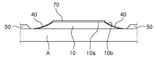
도 19 및 도 20은 본 발명의 일 실시 형태에 따른 반도체 소자를 패키지에 적용한 예를 개략적으로 나타내는 단면도이다.
도 21은 본 발명에 채용가능한 파장변환물질을 설명하기 위한 CIE1931 좌표계이다.
도 22 및 도 23은 본 발명의 일 실시 형태에 따른 반도체 소자를 백라이트 유닛에 적용한 예를 나타내는 단면도이다.
도 24 및 도 25는 본 발명의 일 실시 형태에 의한 반도체 소자를 조명 장치에 적용한 예를 나타내는 분해사시도이다.
도 26 및 도 27은 본 발명의 일 실시 형태에 따른 조명 장치를 이용한 조명 시스템이 적용되는 홈 네트워크를 개략적으로 나타내는 도면이다.
10, 10'... UBM 층
20... 금속간 화합물
30... 솔더 범프
40... 배리어 층
50... 패시베이션 층
100... 반도체 소자
Claims (20)
- AlxInyGa(1-x-y)N로 이루어진 (여기서, 0≤x<1, 0≤y<1, 0≤x+y<1임) 제1 및 제2 도전형 반도체층, 및 상기 제1 및 제2 반도체층 사이에 배치되는 활성층을 포함하는 발광 구조물; 및
상기 발광 구조물의 제1 및 제2 도전형 반도체층의 적어도 하나의 전극 상에 배치되며, 상기 전극의 표면과 반대에 위치한 제1면 및 상기 제1면의 가장자리에서 연장되어 상기 전극과 연결되는 제2면을 가지는 UBM(Under Bump Metallurgy) 층;
상기 제1면 상에 배치되는 금속간 화합물;
상기 금속간 화합물을 매개로 상기 UBM 층과 결속되는 솔더 범프; 및
상기 제2면 상에 배치되며, 상기 UBM 층의 구성원소 중 적어도 하나를 함유한 산화막을 포함하고, 상기 솔더 범프가 상기 제2면으로 확산되는 것을 억제하기 위한 배리어 층;을 포함하는 상호연결용 범프를 포함하는 반도체 소자.
- 제1항에 있어서,
상기 배리어 층 상에는 상기 금속간 화합물 또는 상기 솔더 범프가 형성되지 않는 것을 특징으로 하는 반도체 소자.
- 삭제
- 제1항에 있어서,
상기 배리어 층은 니켈(Ni) 및 구리(Cu) 중 적어도 하나의 원소를 함유한 산화막을 포함하는 것을 특징으로 하는 반도체 소자.
- 제1항에 있어서,
상기 배리어 층은 상기 UBM 층보다 상기 금속간 화합물 및 상기 솔더 범프에 대한 젖음성(wettability)이 작은 것을 특징으로 하는 반도체 소자.
- 제1항에 있어서,
상기 제2면은 상기 제1면에서 상기 전극을 향해 완만하게 경사진 구조를 가지는 것을 특징으로 하는 반도체 소자.
- 제1항에 있어서,
상기 제2면은 상기 전극의 표면과 수직인 구조를 가지는 것을 특징으로 하는 반도체 소자.
- 반도체 소자의 전극 상에 배치되며, 상기 전극의 표면과 반대에 위치한 제1면 및 상기 제1면의 가장자리에서 경사지게 연장되어 상기 전극과 연결되는 측면인 제2면을 가지는 UBM(Under Bump Metallurgy) 층;
상기 제1면 상에 배치되는 금속간 화합물;
상기 금속간 화합물을 매개로 상기 UBM 층과 결속되는 솔더 범프; 및
상기 솔더 범프의 하부에 배치되고, 상기 제2면 상에서 상기 제2면을 따라 연장되도록 배치되며, 상기 UBM 층의 구성원소 중 적어도 하나를 함유한 산화막을 포함하고, 상기 솔더 범프가 상기 제2면으로 확산되는 것을 억제하기 위한 배리어 층을 포함하는 상호연결용 범프.
- 패키지 본체;
상기 패키지 본체에 실장되는 상기 제1항의 반도체 소자; 및
상기 반도체 소자를 봉지하는 봉지부;
를 포함하는 반도체 소자 패키지.
- 하우징; 및
상기 하우징에 장착되는 적어도 하나의 반도체 소자 패키지를 포함하며,
상기 적어도 하나의 반도체 소자 패키지는 상기 제9항의 반도체 소자 패키지인 것을 특징으로 하는 조명 장치. - 삭제
- 삭제
- 삭제
- 삭제
- 삭제
- 삭제
- 삭제
- 삭제
- 삭제
- 삭제
Priority Applications (4)
| Application Number | Priority Date | Filing Date | Title |
|---|---|---|---|
| KR1020140154974A KR102307062B1 (ko) | 2014-11-10 | 2014-11-10 | 반도체 소자, 반도체 소자 패키지 및 조명 장치 |
| US14/729,619 US9583687B2 (en) | 2014-11-10 | 2015-06-03 | Semiconductor device, semiconductor device package, and lightning apparatus |
| CN201510760915.7A CN105591016B (zh) | 2014-11-10 | 2015-11-10 | 互连凸块、半导体器件、半导体器件封装件和照明设备 |
| US15/393,811 US9899584B2 (en) | 2014-11-10 | 2016-12-29 | Semiconductor device and package including solder bumps with strengthened intermetallic compound |
Applications Claiming Priority (1)
| Application Number | Priority Date | Filing Date | Title |
|---|---|---|---|
| KR1020140154974A KR102307062B1 (ko) | 2014-11-10 | 2014-11-10 | 반도체 소자, 반도체 소자 패키지 및 조명 장치 |
Publications (2)
| Publication Number | Publication Date |
|---|---|
| KR20160056330A KR20160056330A (ko) | 2016-05-20 |
| KR102307062B1 true KR102307062B1 (ko) | 2021-10-05 |
Family
ID=55912934
Family Applications (1)
| Application Number | Title | Priority Date | Filing Date |
|---|---|---|---|
| KR1020140154974A Active KR102307062B1 (ko) | 2014-11-10 | 2014-11-10 | 반도체 소자, 반도체 소자 패키지 및 조명 장치 |
Country Status (3)
| Country | Link |
|---|---|
| US (2) | US9583687B2 (ko) |
| KR (1) | KR102307062B1 (ko) |
| CN (1) | CN105591016B (ko) |
Families Citing this family (17)
| Publication number | Priority date | Publication date | Assignee | Title |
|---|---|---|---|---|
| US9425136B2 (en) | 2012-04-17 | 2016-08-23 | Taiwan Semiconductor Manufacturing Company, Ltd. | Conical-shaped or tier-shaped pillar connections |
| US9299674B2 (en) | 2012-04-18 | 2016-03-29 | Taiwan Semiconductor Manufacturing Company, Ltd. | Bump-on-trace interconnect |
| US9111817B2 (en) | 2012-09-18 | 2015-08-18 | Taiwan Semiconductor Manufacturing Company, Ltd. | Bump structure and method of forming same |
| US10269752B2 (en) * | 2014-09-15 | 2019-04-23 | Taiwan Semiconductor Manufacturing Company, Ltd. | Package with UBM and methods of forming |
| US10147692B2 (en) | 2014-09-15 | 2018-12-04 | Taiwan Semiconductor Manufacturing Company, Ltd. | Package with UBM and methods of forming |
| CN109983589B (zh) * | 2015-12-29 | 2022-04-12 | 亮锐控股有限公司 | 具有侧面反射器和磷光体的倒装芯片led |
| KR102601553B1 (ko) | 2016-12-08 | 2023-11-15 | 삼성전자주식회사 | 반도체 발광 소자 |
| JP6297741B1 (ja) | 2017-03-31 | 2018-03-20 | 旭化成エレクトロニクス株式会社 | 光デバイス及びその製造方法 |
| US10879420B2 (en) | 2018-07-09 | 2020-12-29 | University Of Iowa Research Foundation | Cascaded superlattice LED system |
| US10937735B2 (en) * | 2018-09-20 | 2021-03-02 | International Business Machines Corporation | Hybrid under-bump metallization component |
| US11329018B2 (en) | 2019-10-23 | 2022-05-10 | International Business Machines Corporation | Forming of bump structure |
| CN110718622B (zh) * | 2019-10-24 | 2020-12-08 | 朝阳微电子科技股份有限公司 | 一种发光二极管器件及其制造方法 |
| DE102020130638A1 (de) | 2019-12-11 | 2021-06-17 | Infineon Technologies Ag | Lotmaterial, schichtstruktur, chipgehäuse, verfahren zum bilden einer schichtstruktur, verfahren zum bilden eines chipgehäuses, chipanordnung und verfahren zum bilden einer chipanordnung |
| CN114122239A (zh) * | 2021-11-05 | 2022-03-01 | 淮安澳洋顺昌光电技术有限公司 | 焊盘、包含该焊盘的半导体器件、封装件、背光单元及照明设备 |
| CN114156398A (zh) * | 2021-12-17 | 2022-03-08 | 淮安澳洋顺昌光电技术有限公司 | 焊料凸块及其焊盘、半导体器件及其制备方法、封装件、背光单元及照明设备 |
| CN116313834B (zh) * | 2023-05-24 | 2023-09-12 | 江西兆驰半导体有限公司 | 晶圆级封装方法及晶圆级封装结构 |
| US20250022820A1 (en) * | 2023-07-10 | 2025-01-16 | Stmicroelectronics International N.V. | Under-bump metallization structures and associated methods of formation |
Citations (10)
| Publication number | Priority date | Publication date | Assignee | Title |
|---|---|---|---|---|
| US20020096764A1 (en) | 2000-10-13 | 2002-07-25 | Min-Lung Huang | Semiconductor device having bump electrode |
| JP2002252372A (ja) * | 2001-02-26 | 2002-09-06 | Nichia Chem Ind Ltd | 発光ダイオード |
| US20050151269A1 (en) | 2003-12-18 | 2005-07-14 | Samsung Electronics Co., Ltd. | UBM for fine pitch solder balland flip-chip packaging method using the same |
| US20060220259A1 (en) | 2005-01-25 | 2006-10-05 | Ke-Hung Chen | Multi-chip structure and method of assembling chips |
| US20060286697A1 (en) | 2005-06-16 | 2006-12-21 | Leem See J | Method for manufacturing light emitting diodes |
| US20100081271A1 (en) | 2008-09-30 | 2010-04-01 | Tokyo Electron Limited | Method of forming a diffusion barrier and adhesion layer for an interconnect structure |
| US20100112353A1 (en) | 2007-04-13 | 2010-05-06 | Sekisui Chemical Co., Ltd. | Electroconductive fine particles, anisotropic electroconductive material, and electroconductive connection structure |
| US20100187687A1 (en) | 2009-01-26 | 2010-07-29 | Yu-Wen Liu | Underbump Metallization Structure |
| US20120009783A1 (en) | 2007-09-21 | 2012-01-12 | Stats Chippac, Ltd. | Solder Bump With Inner Core Pillar in Semiconductor Package |
| JP2012190939A (ja) * | 2011-03-09 | 2012-10-04 | Panasonic Corp | 半導体装置およびその製造方法 |
Family Cites Families (49)
| Publication number | Priority date | Publication date | Assignee | Title |
|---|---|---|---|---|
| EP0858110B1 (en) | 1996-08-27 | 2006-12-13 | Seiko Epson Corporation | Separating method, method for transferring thin film device, and liquid crystal display device manufactured by using the transferring method |
| USRE38466E1 (en) | 1996-11-12 | 2004-03-16 | Seiko Epson Corporation | Manufacturing method of active matrix substrate, active matrix substrate and liquid crystal display device |
| US6441487B2 (en) * | 1997-10-20 | 2002-08-27 | Flip Chip Technologies, L.L.C. | Chip scale package using large ductile solder balls |
| US7208725B2 (en) | 1998-11-25 | 2007-04-24 | Rohm And Haas Electronic Materials Llc | Optoelectronic component with encapsulant |
| JP2003520449A (ja) | 2000-01-20 | 2003-07-02 | コーニンクレッカ フィリップス エレクトロニクス エヌ ヴィ | ダマスク構造体とダマスク構造体を形成する方法 |
| KR20020007058A (ko) | 2000-07-15 | 2002-01-26 | 최희규 | 고기양념용 기능성 한방추출액 |
| JP3906654B2 (ja) | 2000-07-18 | 2007-04-18 | ソニー株式会社 | 半導体発光素子及び半導体発光装置 |
| KR20020060307A (ko) | 2001-01-10 | 2002-07-18 | 윤종용 | 솔더 범프의 형성 방법 |
| KR20020070584A (ko) | 2001-03-02 | 2002-09-10 | 삼성테크윈 주식회사 | 언더 범프 메탈의 제조방법 및 그 구조 |
| KR20030006691A (ko) | 2001-07-14 | 2003-01-23 | 삼성전자 주식회사 | 글라스 리드의 절단방법 |
| CN1241272C (zh) | 2001-08-22 | 2006-02-08 | 索尼公司 | 氮化物半导体器件及其制造方法 |
| JP2003218034A (ja) | 2002-01-17 | 2003-07-31 | Sony Corp | 選択成長方法、半導体発光素子及びその製造方法 |
| JP3815335B2 (ja) | 2002-01-18 | 2006-08-30 | ソニー株式会社 | 半導体発光素子及びその製造方法 |
| KR100455678B1 (ko) | 2002-02-06 | 2004-11-06 | 마이크로스케일 주식회사 | 반도체 플립칩 패키지를 위한 솔더 범프 구조 및 그 제조방법 |
| DE10231467B4 (de) | 2002-07-08 | 2004-05-27 | Schott Glas | Absorberrohr für solarthermische Anwendungen |
| KR100499129B1 (ko) | 2002-09-02 | 2005-07-04 | 삼성전기주식회사 | 발광 다이오드 및 그 제조방법 |
| US7002182B2 (en) | 2002-09-06 | 2006-02-21 | Sony Corporation | Semiconductor light emitting device integral type semiconductor light emitting unit image display unit and illuminating unit |
| JP2004207685A (ja) | 2002-12-23 | 2004-07-22 | Samsung Electronics Co Ltd | 無鉛ソルダバンプの製造方法 |
| KR100534108B1 (ko) | 2002-12-23 | 2005-12-08 | 삼성전자주식회사 | 무연 솔더범프 제조 방법 |
| KR100714639B1 (ko) | 2003-10-21 | 2007-05-07 | 삼성전기주식회사 | 발광 소자 |
| KR100506740B1 (ko) | 2003-12-23 | 2005-08-08 | 삼성전기주식회사 | 질화물 반도체 발광소자 및 그 제조방법 |
| TWI230425B (en) * | 2004-02-06 | 2005-04-01 | South Epitaxy Corp | Bumping process for light emitting diode |
| KR100664985B1 (ko) | 2004-10-26 | 2007-01-09 | 삼성전기주식회사 | 질화물계 반도체 소자 |
| US7868345B2 (en) * | 2004-10-27 | 2011-01-11 | Kyocera Corporation | Light emitting device mounting substrate, light emitting device housing package, light emitting apparatus, and illuminating apparatus |
| JP2006278551A (ja) * | 2005-03-28 | 2006-10-12 | Fujitsu Ltd | 半導体装置及びその製造方法 |
| KR100717834B1 (ko) | 2005-07-13 | 2007-05-11 | 최용재 | 통신망을 이용한 원격 아토피 진단시스템 및 그 진단방법 |
| KR100665222B1 (ko) | 2005-07-26 | 2007-01-09 | 삼성전기주식회사 | 확산재료를 이용한 엘이디 패키지 및 그 제조 방법 |
| US7952206B2 (en) | 2005-09-27 | 2011-05-31 | Agere Systems Inc. | Solder bump structure for flip chip semiconductor devices and method of manufacture therefore |
| KR100661614B1 (ko) | 2005-10-07 | 2006-12-26 | 삼성전기주식회사 | 질화물계 반도체 발광소자 및 그 제조방법 |
| KR100723247B1 (ko) | 2006-01-10 | 2007-05-29 | 삼성전기주식회사 | 칩코팅형 led 패키지 및 그 제조방법 |
| KR100859641B1 (ko) | 2006-02-20 | 2008-09-23 | 주식회사 네패스 | 금속간 화합물 성장을 억제시킨 솔더 범프가 형성된 반도체칩 및 제조 방법 |
| KR100735325B1 (ko) | 2006-04-17 | 2007-07-04 | 삼성전기주식회사 | 발광다이오드 패키지 및 그 제조방법 |
| KR100930171B1 (ko) * | 2006-12-05 | 2009-12-07 | 삼성전기주식회사 | 백색 발광장치 및 이를 이용한 백색 광원 모듈 |
| US20080251916A1 (en) * | 2007-04-12 | 2008-10-16 | Taiwan Semiconductor Manufacturing Company, Ltd. | UBM structure for strengthening solder bumps |
| KR100855065B1 (ko) | 2007-04-24 | 2008-08-29 | 삼성전기주식회사 | 발광 다이오드 패키지 |
| KR100982980B1 (ko) | 2007-05-15 | 2010-09-17 | 삼성엘이디 주식회사 | 면 광원 장치 및 이를 구비하는 lcd 백라이트 유닛 |
| KR101164026B1 (ko) | 2007-07-12 | 2012-07-18 | 삼성전자주식회사 | 질화물계 반도체 발광소자 및 그 제조방법 |
| KR100891761B1 (ko) | 2007-10-19 | 2009-04-07 | 삼성전기주식회사 | 반도체 발광소자, 그의 제조방법 및 이를 이용한 반도체발광소자 패키지 |
| US7727882B1 (en) * | 2007-12-17 | 2010-06-01 | Novellus Systems, Inc. | Compositionally graded titanium nitride film for diffusion barrier applications |
| KR101332794B1 (ko) | 2008-08-05 | 2013-11-25 | 삼성전자주식회사 | 발광 장치, 이를 포함하는 발광 시스템, 상기 발광 장치 및발광 시스템의 제조 방법 |
| KR20100030470A (ko) | 2008-09-10 | 2010-03-18 | 삼성전자주식회사 | 다양한 색 온도의 백색광을 제공할 수 있는 발광 장치 및 발광 시스템 |
| KR101530876B1 (ko) | 2008-09-16 | 2015-06-23 | 삼성전자 주식회사 | 발광량이 증가된 발광 소자, 이를 포함하는 발광 장치, 상기 발광 소자 및 발광 장치의 제조 방법 |
| US8008683B2 (en) | 2008-10-22 | 2011-08-30 | Samsung Led Co., Ltd. | Semiconductor light emitting device |
| US8003512B2 (en) | 2009-02-03 | 2011-08-23 | International Business Machines Corporation | Structure of UBM and solder bumps and methods of fabrication |
| JP5263053B2 (ja) * | 2009-07-24 | 2013-08-14 | 株式会社村田製作所 | 半導体パッケージおよび半導体パッケージモジュール |
| US8405199B2 (en) * | 2010-07-08 | 2013-03-26 | Taiwan Semiconductor Manufacturing Company, Ltd. | Conductive pillar for semiconductor substrate and method of manufacture |
| KR20120009868A (ko) * | 2010-07-22 | 2012-02-02 | 앰코 테크놀로지 코리아 주식회사 | 발광 다이오드 패키지 및 그 제조 방법 |
| US8492892B2 (en) | 2010-12-08 | 2013-07-23 | International Business Machines Corporation | Solder bump connections |
| US8692378B2 (en) | 2011-12-06 | 2014-04-08 | Taiwan Semiconductor Manufacturing Company, Ltd. | UBM structures for wafer level chip scale packaging |
-
2014
- 2014-11-10 KR KR1020140154974A patent/KR102307062B1/ko active Active
-
2015
- 2015-06-03 US US14/729,619 patent/US9583687B2/en active Active
- 2015-11-10 CN CN201510760915.7A patent/CN105591016B/zh active Active
-
2016
- 2016-12-29 US US15/393,811 patent/US9899584B2/en active Active
Patent Citations (10)
| Publication number | Priority date | Publication date | Assignee | Title |
|---|---|---|---|---|
| US20020096764A1 (en) | 2000-10-13 | 2002-07-25 | Min-Lung Huang | Semiconductor device having bump electrode |
| JP2002252372A (ja) * | 2001-02-26 | 2002-09-06 | Nichia Chem Ind Ltd | 発光ダイオード |
| US20050151269A1 (en) | 2003-12-18 | 2005-07-14 | Samsung Electronics Co., Ltd. | UBM for fine pitch solder balland flip-chip packaging method using the same |
| US20060220259A1 (en) | 2005-01-25 | 2006-10-05 | Ke-Hung Chen | Multi-chip structure and method of assembling chips |
| US20060286697A1 (en) | 2005-06-16 | 2006-12-21 | Leem See J | Method for manufacturing light emitting diodes |
| US20100112353A1 (en) | 2007-04-13 | 2010-05-06 | Sekisui Chemical Co., Ltd. | Electroconductive fine particles, anisotropic electroconductive material, and electroconductive connection structure |
| US20120009783A1 (en) | 2007-09-21 | 2012-01-12 | Stats Chippac, Ltd. | Solder Bump With Inner Core Pillar in Semiconductor Package |
| US20100081271A1 (en) | 2008-09-30 | 2010-04-01 | Tokyo Electron Limited | Method of forming a diffusion barrier and adhesion layer for an interconnect structure |
| US20100187687A1 (en) | 2009-01-26 | 2010-07-29 | Yu-Wen Liu | Underbump Metallization Structure |
| JP2012190939A (ja) * | 2011-03-09 | 2012-10-04 | Panasonic Corp | 半導体装置およびその製造方法 |
Also Published As
| Publication number | Publication date |
|---|---|
| US9899584B2 (en) | 2018-02-20 |
| KR20160056330A (ko) | 2016-05-20 |
| US9583687B2 (en) | 2017-02-28 |
| CN105591016A (zh) | 2016-05-18 |
| CN105591016B (zh) | 2018-05-08 |
| US20160133807A1 (en) | 2016-05-12 |
| US20170110639A1 (en) | 2017-04-20 |
Similar Documents
| Publication | Publication Date | Title |
|---|---|---|
| KR102307062B1 (ko) | 반도체 소자, 반도체 소자 패키지 및 조명 장치 | |
| KR102282137B1 (ko) | 반도체 발광소자 및 이를 구비한 반도체 발광장치 | |
| KR102443033B1 (ko) | 발광소자 패키지 및 이를 포함하는 조명 장치 | |
| KR102374268B1 (ko) | 발광소자 패키지 | |
| KR102530759B1 (ko) | 발광소자 패키지 및 그 제조방법 | |
| KR102427641B1 (ko) | 반도체 발광소자 | |
| KR102417181B1 (ko) | 발광 패키지, 반도체 발광 소자, 발광 모듈 및 발광 패키지의 제조 방법 | |
| US9548426B2 (en) | Semiconductor light-emitting device | |
| US9887332B2 (en) | Semiconductor light-emitting device package | |
| US20160163663A1 (en) | Semiconductor light-emitting device and semiconductor light-emitting apparatus having the same | |
| KR102223038B1 (ko) | 반도체 발광소자 및 이를 구비한 반도체 발광장치 | |
| US9666754B2 (en) | Method of manufacturing semiconductor substrate and substrate for semiconductor growth | |
| CN106410004A (zh) | 半导体发光器件及其制造方法 | |
| TW202339302A (zh) | 用於電流注入之led晶片的接觸結構 | |
| KR20160056167A (ko) | 발광 장치의 제조 방법, 발광 모듈 검사 장비 및 발광 모듈의 양불 판단 방법 | |
| US9899565B2 (en) | Method of manufacturing semiconductor substrate including separating two semiconductor layers from a growth substrate | |
| KR20160145888A (ko) | 발광소자 패키지 | |
| KR20150117911A (ko) | 조명 장치 | |
| KR20160101226A (ko) | 반도체 발광 소자 |
Legal Events
| Date | Code | Title | Description |
|---|---|---|---|
| PA0109 | Patent application |
St.27 status event code: A-0-1-A10-A12-nap-PA0109 |
|
| PG1501 | Laying open of application |
St.27 status event code: A-1-1-Q10-Q12-nap-PG1501 |
|
| E13-X000 | Pre-grant limitation requested |
St.27 status event code: A-2-3-E10-E13-lim-X000 |
|
| P11-X000 | Amendment of application requested |
St.27 status event code: A-2-2-P10-P11-nap-X000 |
|
| P13-X000 | Application amended |
St.27 status event code: A-2-2-P10-P13-nap-X000 |
|
| PA0201 | Request for examination |
St.27 status event code: A-1-2-D10-D11-exm-PA0201 |
|
| E902 | Notification of reason for refusal | ||
| PE0902 | Notice of grounds for rejection |
St.27 status event code: A-1-2-D10-D21-exm-PE0902 |
|
| E13-X000 | Pre-grant limitation requested |
St.27 status event code: A-2-3-E10-E13-lim-X000 |
|
| P11-X000 | Amendment of application requested |
St.27 status event code: A-2-2-P10-P11-nap-X000 |
|
| P13-X000 | Application amended |
St.27 status event code: A-2-2-P10-P13-nap-X000 |
|
| E90F | Notification of reason for final refusal | ||
| PE0902 | Notice of grounds for rejection |
St.27 status event code: A-1-2-D10-D21-exm-PE0902 |
|
| P11-X000 | Amendment of application requested |
St.27 status event code: A-2-2-P10-P11-nap-X000 |
|
| P13-X000 | Application amended |
St.27 status event code: A-2-2-P10-P13-nap-X000 |
|
| E701 | Decision to grant or registration of patent right | ||
| PE0701 | Decision of registration |
St.27 status event code: A-1-2-D10-D22-exm-PE0701 |
|
| PR0701 | Registration of establishment |
St.27 status event code: A-2-4-F10-F11-exm-PR0701 |
|
| PR1002 | Payment of registration fee |
St.27 status event code: A-2-2-U10-U11-oth-PR1002 Fee payment year number: 1 |
|
| PG1601 | Publication of registration |
St.27 status event code: A-4-4-Q10-Q13-nap-PG1601 |
|
| PR1001 | Payment of annual fee |
St.27 status event code: A-4-4-U10-U11-oth-PR1001 Fee payment year number: 4 |
|
| P22-X000 | Classification modified |
St.27 status event code: A-4-4-P10-P22-nap-X000 |
|
| PR1001 | Payment of annual fee |
St.27 status event code: A-4-4-U10-U11-oth-PR1001 Fee payment year number: 5 |
|
| U11 | Full renewal or maintenance fee paid |
Free format text: ST27 STATUS EVENT CODE: A-4-4-U10-U11-OTH-PR1001 (AS PROVIDED BY THE NATIONAL OFFICE) Year of fee payment: 5 |