KR102246292B1 - 휴대용 전자장치 - Google Patents
휴대용 전자장치 Download PDFInfo
- Publication number
- KR102246292B1 KR102246292B1 KR1020140096757A KR20140096757A KR102246292B1 KR 102246292 B1 KR102246292 B1 KR 102246292B1 KR 1020140096757 A KR1020140096757 A KR 1020140096757A KR 20140096757 A KR20140096757 A KR 20140096757A KR 102246292 B1 KR102246292 B1 KR 102246292B1
- Authority
- KR
- South Korea
- Prior art keywords
- adhesive layer
- display panel
- area
- patterned
- portable electronic
- Prior art date
- Legal status (The legal status is an assumption and is not a legal conclusion. Google has not performed a legal analysis and makes no representation as to the accuracy of the status listed.)
- Expired - Fee Related
Links
- 239000012790 adhesive layer Substances 0.000 claims abstract description 150
- 239000011159 matrix material Substances 0.000 claims description 14
- 238000000034 method Methods 0.000 claims description 14
- 239000000853 adhesive Substances 0.000 claims description 12
- 230000001070 adhesive effect Effects 0.000 claims description 12
- 239000010410 layer Substances 0.000 claims description 7
- 238000005452 bending Methods 0.000 abstract description 40
- 230000007547 defect Effects 0.000 abstract description 4
- 239000013256 coordination polymer Substances 0.000 description 11
- 239000004642 Polyimide Substances 0.000 description 3
- 239000004820 Pressure-sensitive adhesive Substances 0.000 description 3
- 230000008878 coupling Effects 0.000 description 3
- 238000010168 coupling process Methods 0.000 description 3
- 238000005859 coupling reaction Methods 0.000 description 3
- 239000000463 material Substances 0.000 description 3
- 229920000139 polyethylene terephthalate Polymers 0.000 description 3
- 239000005020 polyethylene terephthalate Substances 0.000 description 3
- 229920001721 polyimide Polymers 0.000 description 3
- 230000000694 effects Effects 0.000 description 2
- 230000004048 modification Effects 0.000 description 2
- 238000012986 modification Methods 0.000 description 2
- -1 polyethylene terephthalate Polymers 0.000 description 2
- 239000004840 adhesive resin Substances 0.000 description 1
- 229920006223 adhesive resin Polymers 0.000 description 1
- 239000000470 constituent Substances 0.000 description 1
- 230000006866 deterioration Effects 0.000 description 1
- 239000011521 glass Substances 0.000 description 1
- 239000011147 inorganic material Substances 0.000 description 1
- 229910010272 inorganic material Inorganic materials 0.000 description 1
- 239000011368 organic material Substances 0.000 description 1
- 230000008569 process Effects 0.000 description 1
- 229920005989 resin Polymers 0.000 description 1
- 239000011347 resin Substances 0.000 description 1
- 239000000758 substrate Substances 0.000 description 1
- 230000009466 transformation Effects 0.000 description 1
- 238000000844 transformation Methods 0.000 description 1
Images


Classifications
-
- G—PHYSICS
- G06—COMPUTING; CALCULATING OR COUNTING
- G06F—ELECTRIC DIGITAL DATA PROCESSING
- G06F1/00—Details not covered by groups G06F3/00 - G06F13/00 and G06F21/00
- G06F1/16—Constructional details or arrangements
- G06F1/1613—Constructional details or arrangements for portable computers
- G06F1/1633—Constructional details or arrangements of portable computers not specific to the type of enclosures covered by groups G06F1/1615 - G06F1/1626
- G06F1/1656—Details related to functional adaptations of the enclosure, e.g. to provide protection against EMI, shock, water, or to host detachable peripherals like a mouse or removable expansions units like PCMCIA cards, or to provide access to internal components for maintenance or to removable storage supports like CDs or DVDs, or to mechanically mount accessories
-
- F—MECHANICAL ENGINEERING; LIGHTING; HEATING; WEAPONS; BLASTING
- F21—LIGHTING
- F21V—FUNCTIONAL FEATURES OR DETAILS OF LIGHTING DEVICES OR SYSTEMS THEREOF; STRUCTURAL COMBINATIONS OF LIGHTING DEVICES WITH OTHER ARTICLES, NOT OTHERWISE PROVIDED FOR
- F21V11/00—Screens not covered by groups F21V1/00, F21V3/00, F21V7/00 or F21V9/00
-
- G—PHYSICS
- G02—OPTICS
- G02F—OPTICAL DEVICES OR ARRANGEMENTS FOR THE CONTROL OF LIGHT BY MODIFICATION OF THE OPTICAL PROPERTIES OF THE MEDIA OF THE ELEMENTS INVOLVED THEREIN; NON-LINEAR OPTICS; FREQUENCY-CHANGING OF LIGHT; OPTICAL LOGIC ELEMENTS; OPTICAL ANALOGUE/DIGITAL CONVERTERS
- G02F1/00—Devices or arrangements for the control of the intensity, colour, phase, polarisation or direction of light arriving from an independent light source, e.g. switching, gating or modulating; Non-linear optics
- G02F1/01—Devices or arrangements for the control of the intensity, colour, phase, polarisation or direction of light arriving from an independent light source, e.g. switching, gating or modulating; Non-linear optics for the control of the intensity, phase, polarisation or colour
- G02F1/13—Devices or arrangements for the control of the intensity, colour, phase, polarisation or direction of light arriving from an independent light source, e.g. switching, gating or modulating; Non-linear optics for the control of the intensity, phase, polarisation or colour based on liquid crystals, e.g. single liquid crystal display cells
- G02F1/133—Constructional arrangements; Operation of liquid crystal cells; Circuit arrangements
-
- H—ELECTRICITY
- H10—SEMICONDUCTOR DEVICES; ELECTRIC SOLID-STATE DEVICES NOT OTHERWISE PROVIDED FOR
- H10K—ORGANIC ELECTRIC SOLID-STATE DEVICES
- H10K50/00—Organic light-emitting devices
Landscapes
- Engineering & Computer Science (AREA)
- Computer Hardware Design (AREA)
- Physics & Mathematics (AREA)
- General Engineering & Computer Science (AREA)
- Theoretical Computer Science (AREA)
- General Physics & Mathematics (AREA)
- Human Computer Interaction (AREA)
- Nonlinear Science (AREA)
- Devices For Indicating Variable Information By Combining Individual Elements (AREA)
- Crystallography & Structural Chemistry (AREA)
- Chemical & Material Sciences (AREA)
- Optics & Photonics (AREA)
- Mathematical Physics (AREA)
- Electroluminescent Light Sources (AREA)
- Liquid Crystal (AREA)
- Microelectronics & Electronic Packaging (AREA)
Abstract
Description
도 2는 도 1의 휴대용 전자장치의 일부분을 개략적으로 도시하는 단면도이다.
도 3은 본 발명의 다른 일 실시예에 따른 휴대용 전자장치의 일부분을 개략적으로 도시하는 단면도이다.
도 4는 본 발명의 또 다른 일 실시예에 따른 휴대용 전자장치의 일부분을 개략적으로 도시하는 단면도이다.
도 5는 본 발명의 또 다른 일 실시예에 따른 휴대용 전자장치의 일부분을 개략적으로 도시하는 평면 개념도이다.
도 6은 본 발명의 또 다른 일 실시예에 따른 휴대용 전자장치의 일부분을 개략적으로 도시하는 평면 개념도이다.
도 7은 본 발명의 또 다른 일 실시예에 따른 휴대용 전자장치의 일부분을 개략적으로 도시하는 평면 개념도이다.
도 8은 본 발명의 또 다른 일 실시예에 따른 휴대용 전자장치의 일부분을 개략적으로 도시하는 단면도이다.
도 9는 도 8의 휴대용 전자장치가 벤딩되는 것을 개략적으로 도시하는 단면도이다.
도 10은 본 발명의 또 다른 일 실시예에 따른 휴대용 전자장치의 일부분을 개략적으로 도시하는 단면도이다.
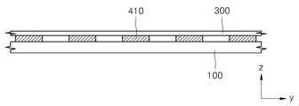
300: 기능판 410: 제1접착층
420: 제2접착층 510: 윈도우
520: 하우징
Claims (17)
- 이미지를 디스플레이할 수 있으며, 화소들 또는 부화소들 사이에 대응하는 블랙매트릭스를 포함하는, 디스플레이 패널;
상기 디스플레이 패널의 이미지 디스플레이 면 상부에 위치한 윈도우;
상기 디스플레이 패널과 상기 윈도우 사이에 개재된 기능판; 및
상기 디스플레이 패널과 상기 기능판 사이 또는 상기 기능판과 상기 윈도우 사이에 개재되며, 패터닝되고, 상기 블랙매트릭스에 대응하는, 제1접착층;
을 구비하는, 휴대용 전자장치. - 제1항에 있어서,
상기 디스플레이 패널의 중앙부에서의 기준면적당 상기 제1접착층의 면적이 상기 디스플레이 패널의 가장자리부에서의 기준면적당 상기 제1접착층의 면적보다 넓은, 휴대용 전자장치. - 이미지를 디스플레이할 수 있는 디스플레이 패널;
상기 디스플레이 패널의 이미지 디스플레이 면 상부에 위치한 윈도우;
상기 디스플레이 패널과 상기 윈도우 사이에 개재된 기능판;
상기 디스플레이 패널과 상기 기능판 사이 또는 상기 기능판과 상기 윈도우 사이에 개재되며 패터닝된 제1접착층; 및
상기 제1접착층의 패턴 사이를 채우며, 상기 제1접착층의 접착력보다 낮은 접착력을 갖는, 보조접착층;
을 구비하는, 휴대용 전자장치. - 삭제
- 삭제
- 제1항에 있어서,
사전설정된 폴딩영역을 가져 상기 폴딩영역에서 접힐 수 있으며, 상기 디스플레이 패널의 상기 폴딩영역에서의 기준면적당 상기 제1접착층의 면적이 상기 디스플레이 패널의 가장자리부에서의 기준면적당 상기 제1접착층의 면적과 상이한, 휴대용 전자장치. - 제6항에 있어서,
상기 디스플레이 패널의 상기 폴딩영역에서의 기준면적당 상기 제1접착층의 면적이 상기 디스플레이 패널의 상기 가장자리부에서의 기준면적당 상기 제1접착층의 면적보다 넓은, 휴대용 전자장치. - 제1항 내지 제3항, 제6항 및 제7항 중 어느 한 항에 있어서,
상기 제1접착층은 아일랜드 형상으로 패터닝된, 휴대용 전자장치. - 제1항 내지 제3항, 제6항 및 제7항 중 어느 한 항에 있어서,
상기 제1접착층은 스트라이프 형상으로 패터닝된, 휴대용 전자장치. - 제9항에 있어서,
상기 제1접착층은 서로 교차하는 스트라이프 형상으로 패터닝된, 휴대용 전자장치. - 제1항 내지 제3항, 제6항 및 제7항 중 어느 한 항에 있어서,
상기 제1접착층은 아일랜드 형상으로 패터닝된 부분과 스트라이프 형상으로 패터닝된 부분을 갖는, 휴대용 전자장치. - 이미지를 디스플레이할 수 있으며, 화소들 또는 부화소들 사이에 대응하는 블랙매트릭스를 포함하는, 디스플레이 패널;
상기 디스플레이 패널의 이미지 디스플레이 면 상부에 위치한 윈도우;
상기 디스플레이 패널과 상기 윈도우 사이에 개재된 기능판;
상기 디스플레이 패널과 상기 기능판 사이에 개재되며, 패터닝되고, 상기 블랙매트릭스에 대응하는, 제1접착층; 및
상기 기능판과 상기 윈도우 사이에 개재되며 패터닝된 제2접착층;
을 구비하는, 휴대용 전자장치. - 제12항에 있어서,
상기 제1접착층의 접착력이 상기 제2접착층의 접착력보다 높은, 휴대용 전자장치. - 제12항에 있어서,
기준면적당 상기 제1접착층의 면적이 기준면적당 상기 제2접착층의 면적보다 넓은, 휴대용 전자장치. - 제12항에 있어서,
상기 제1접착층은 스트라이프 형상으로 패터닝되고, 상기 제2접착층은 아일랜드 형상으로 패터닝된, 휴대용 전자장치. - 제12항에 있어서,
상기 제1접착층은 아일랜드 형상으로 패터닝된 부분과 스트라이프 형상으로 패터닝된 부분을 갖고, 상기 제2접착층은 스트라이프 형상만으로 패터닝되거나 아일랜드 형상만으로 패터닝된, 휴대용 전자장치. - 제1항 내지 제3항, 제6항, 제7항 및 제12항 내지 제16항 중 어느 한 항에 있어서,
상기 기능판은 편광판, 위상지연판 또는 터치패널을 포함하는, 휴대용 전자장치.
Priority Applications (3)
| Application Number | Priority Date | Filing Date | Title |
|---|---|---|---|
| KR1020140096757A KR102246292B1 (ko) | 2014-07-29 | 2014-07-29 | 휴대용 전자장치 |
| US14/656,561 US9977468B2 (en) | 2014-07-29 | 2015-03-12 | Portable electronic apparatus |
| US15/985,651 US10254800B2 (en) | 2014-07-29 | 2018-05-21 | Portable electronic apparatus |
Applications Claiming Priority (1)
| Application Number | Priority Date | Filing Date | Title |
|---|---|---|---|
| KR1020140096757A KR102246292B1 (ko) | 2014-07-29 | 2014-07-29 | 휴대용 전자장치 |
Publications (2)
| Publication Number | Publication Date |
|---|---|
| KR20160014872A KR20160014872A (ko) | 2016-02-12 |
| KR102246292B1 true KR102246292B1 (ko) | 2021-04-30 |
Family
ID=55181613
Family Applications (1)
| Application Number | Title | Priority Date | Filing Date |
|---|---|---|---|
| KR1020140096757A Expired - Fee Related KR102246292B1 (ko) | 2014-07-29 | 2014-07-29 | 휴대용 전자장치 |
Country Status (2)
| Country | Link |
|---|---|
| US (2) | US9977468B2 (ko) |
| KR (1) | KR102246292B1 (ko) |
Families Citing this family (15)
| Publication number | Priority date | Publication date | Assignee | Title |
|---|---|---|---|---|
| US20180072920A1 (en) * | 2015-04-10 | 2018-03-15 | Kaneka Corporation | Graphite composite film and method for producing same, and heat-dissipating part |
| US9578768B1 (en) | 2015-09-10 | 2017-02-21 | Apple Inc. | Laser-colored sapphire material |
| KR102069286B1 (ko) * | 2015-11-20 | 2020-01-22 | 동우 화인켐 주식회사 | 플렉서블 표시 장치 |
| KR102533171B1 (ko) * | 2016-03-11 | 2023-05-18 | 삼성디스플레이 주식회사 | 플렉서블 표시장치 |
| KR102455724B1 (ko) * | 2016-04-21 | 2022-10-19 | 삼성디스플레이 주식회사 | 플렉서블 표시 장치 |
| KR102146150B1 (ko) * | 2016-10-03 | 2020-08-19 | 김영수 | 탈부착 패턴을 가진 디스플레이 장치 |
| TWI627777B (zh) * | 2017-07-26 | 2018-06-21 | 財團法人工業技術研究院 | 光學補償結構 |
| KR102426365B1 (ko) | 2017-08-21 | 2022-07-29 | 삼성전자 주식회사 | 안테나를 포함하는 전자 장치 |
| US10903435B2 (en) * | 2017-10-18 | 2021-01-26 | Dongwoo Fine-Chem Co., Ltd. | Flexible display device |
| KR102508251B1 (ko) * | 2017-11-28 | 2023-03-08 | 엘지디스플레이 주식회사 | 폴더블 표시장치 |
| KR102241293B1 (ko) * | 2018-05-14 | 2021-04-16 | 김영수 | 점착조절층을 이용한 표시장치 |
| CN111866232A (zh) * | 2019-04-29 | 2020-10-30 | 北京小米移动软件有限公司 | 屏幕模组及电子设备 |
| US20220390983A1 (en) * | 2019-08-19 | 2022-12-08 | Boe Technology Group Co., Ltd. | Foldable display screen and manufacturing method thereof, and display apparatus |
| CN210514868U (zh) * | 2019-11-18 | 2020-05-12 | 京东方科技集团股份有限公司 | 一种显示装置 |
| CN113539094A (zh) | 2021-07-14 | 2021-10-22 | 武汉华星光电半导体显示技术有限公司 | 显示面板及显示装置 |
Family Cites Families (14)
| Publication number | Priority date | Publication date | Assignee | Title |
|---|---|---|---|---|
| JPH02282225A (ja) * | 1988-10-24 | 1990-11-19 | Ricoh Co Ltd | 液晶表示素子 |
| US5739946A (en) * | 1995-09-21 | 1998-04-14 | Kabushiki Kaisha Toshiba | Display device |
| KR101303816B1 (ko) * | 2006-06-30 | 2013-09-04 | 엘지디스플레이 주식회사 | 액정 표시 장치용 모기판, 이를 이용한 액정 표시 장치 및액정 표시 장치의 제조 방법 |
| JP2008116880A (ja) | 2006-11-08 | 2008-05-22 | Toppan Printing Co Ltd | 液晶表示装置用カラーフィルターへのスペーサービーズ形成方法および液晶表示素子の製造方法 |
| JP4978997B2 (ja) | 2006-12-25 | 2012-07-18 | 株式会社ジャパンディスプレイイースト | 表示装置の製造方法 |
| JP5283944B2 (ja) * | 2008-03-25 | 2013-09-04 | 株式会社東芝 | 表示装置 |
| KR101870185B1 (ko) | 2011-12-09 | 2018-06-25 | 엘지디스플레이 주식회사 | 표시장치와 이의 제조방법 |
| KR101880114B1 (ko) | 2012-02-08 | 2018-08-20 | 삼성디스플레이 주식회사 | 표시 장치 |
| KR101996652B1 (ko) * | 2012-11-01 | 2019-07-05 | 삼성디스플레이 주식회사 | 표시 장치 |
| KR102078831B1 (ko) * | 2013-03-12 | 2020-04-03 | 삼성디스플레이 주식회사 | 플렉서블 터치 스크린 패널을 구비한 플렉서블 표시장치 |
| KR20140123735A (ko) * | 2013-04-15 | 2014-10-23 | 삼성디스플레이 주식회사 | 점착캡슐을 갖는 점착제 및 상기 점착제에 의하여 형성된 점착층을 갖는 유기발광 표시장치 |
| KR102135453B1 (ko) * | 2013-05-24 | 2020-07-20 | 삼성디스플레이 주식회사 | 접착필름 및 이를 이용해 제조된 유기전계발광 표시장치 |
| KR102051916B1 (ko) * | 2013-09-27 | 2019-12-04 | 엘지디스플레이 주식회사 | 강화기판이 부착된 표시소자 |
| KR20150084257A (ko) | 2014-01-13 | 2015-07-22 | 삼성디스플레이 주식회사 | 플렉서블 표시장치 |
-
2014
- 2014-07-29 KR KR1020140096757A patent/KR102246292B1/ko not_active Expired - Fee Related
-
2015
- 2015-03-12 US US14/656,561 patent/US9977468B2/en active Active
-
2018
- 2018-05-21 US US15/985,651 patent/US10254800B2/en active Active
Also Published As
| Publication number | Publication date |
|---|---|
| KR20160014872A (ko) | 2016-02-12 |
| US20160037656A1 (en) | 2016-02-04 |
| US20180267576A1 (en) | 2018-09-20 |
| US9977468B2 (en) | 2018-05-22 |
| US10254800B2 (en) | 2019-04-09 |
Similar Documents
| Publication | Publication Date | Title |
|---|---|---|
| KR102246292B1 (ko) | 휴대용 전자장치 | |
| KR102511547B1 (ko) | 표시 장치 및 휴대용 단말기 | |
| US8884889B2 (en) | Display device having a touch screen panel and manufacturing method thereof | |
| US9947882B2 (en) | Electronic devices with robust flexible displays | |
| KR102648415B1 (ko) | 터치 스크린 일체형 표시 장치 및 그 제조 방법 | |
| US11668983B2 (en) | Display apparatus | |
| US10698249B2 (en) | Window substrate, method of manufacturing the same and image display device including the same | |
| JP2020034916A (ja) | フォルダブル表示装置 | |
| KR102408410B1 (ko) | 폴더블 표시 장치 | |
| WO2019047591A1 (zh) | 可折弯盖板、可折弯显示模组及可折弯终端设备 | |
| KR20220022939A (ko) | 표시 장치 및 이를 포함하는 전자 장치 | |
| KR20140101601A (ko) | 영상 표시 장치 | |
| KR102654660B1 (ko) | 폴더블 표시 장치 | |
| JP2013134782A (ja) | タッチパネル | |
| KR102775200B1 (ko) | 표시 장치 및 그것의 제조 방법 | |
| CN112018151A (zh) | 显示设备和制造显示设备的方法 | |
| KR102797604B1 (ko) | 표시 장치 | |
| KR102337614B1 (ko) | 윈도우 기판의 제조 방법 | |
| KR102715075B1 (ko) | 표시 장치 | |
| CN114613257A (zh) | 显示装置及显示设备 | |
| KR102611476B1 (ko) | 편광 필름, 상기 편광 필름을 포함하는 표시 장치, 및 상기 편광 필름의 제조 방법 | |
| EP2808731A2 (en) | Display device comprising protective films | |
| CN116472792A (zh) | 具有抗冲击层的显示装置 | |
| KR102535371B1 (ko) | 디스플레이용 커버 기재 및 이를 포함하는 디스플레이 장치 | |
| CN222014948U (zh) | 显示装置 |
Legal Events
| Date | Code | Title | Description |
|---|---|---|---|
| PA0109 | Patent application |
Patent event code: PA01091R01D Comment text: Patent Application Patent event date: 20140729 |
|
| PG1501 | Laying open of application | ||
| A201 | Request for examination | ||
| PA0201 | Request for examination |
Patent event code: PA02012R01D Patent event date: 20190729 Comment text: Request for Examination of Application Patent event code: PA02011R01I Patent event date: 20140729 Comment text: Patent Application |
|
| E902 | Notification of reason for refusal | ||
| PE0902 | Notice of grounds for rejection |
Comment text: Notification of reason for refusal Patent event date: 20200824 Patent event code: PE09021S01D |
|
| E701 | Decision to grant or registration of patent right | ||
| PE0701 | Decision of registration |
Patent event code: PE07011S01D Comment text: Decision to Grant Registration Patent event date: 20210205 |
|
| PR0701 | Registration of establishment |
Comment text: Registration of Establishment Patent event date: 20210423 Patent event code: PR07011E01D |
|
| PR1002 | Payment of registration fee |
Payment date: 20210426 End annual number: 3 Start annual number: 1 |
|
| PG1601 | Publication of registration | ||
| PC1903 | Unpaid annual fee |
Termination category: Default of registration fee Termination date: 20250204 |