KR102182525B1 - Semiconductor device and method for manufacturing the same - Google Patents
Semiconductor device and method for manufacturing the same Download PDFInfo
- Publication number
- KR102182525B1 KR102182525B1 KR1020130159893A KR20130159893A KR102182525B1 KR 102182525 B1 KR102182525 B1 KR 102182525B1 KR 1020130159893 A KR1020130159893 A KR 1020130159893A KR 20130159893 A KR20130159893 A KR 20130159893A KR 102182525 B1 KR102182525 B1 KR 102182525B1
- Authority
- KR
- South Korea
- Prior art keywords
- film
- insulating film
- oxide
- electrode
- semiconductor film
- Prior art date
- Legal status (The legal status is an assumption and is not a legal conclusion. Google has not performed a legal analysis and makes no representation as to the accuracy of the status listed.)
- Expired - Fee Related
Links
Images


Classifications
-
- H—ELECTRICITY
- H10—SEMICONDUCTOR DEVICES; ELECTRIC SOLID-STATE DEVICES NOT OTHERWISE PROVIDED FOR
- H10D—INORGANIC ELECTRIC SEMICONDUCTOR DEVICES
- H10D30/00—Field-effect transistors [FET]
- H10D30/60—Insulated-gate field-effect transistors [IGFET]
- H10D30/67—Thin-film transistors [TFT]
-
- G—PHYSICS
- G02—OPTICS
- G02F—OPTICAL DEVICES OR ARRANGEMENTS FOR THE CONTROL OF LIGHT BY MODIFICATION OF THE OPTICAL PROPERTIES OF THE MEDIA OF THE ELEMENTS INVOLVED THEREIN; NON-LINEAR OPTICS; FREQUENCY-CHANGING OF LIGHT; OPTICAL LOGIC ELEMENTS; OPTICAL ANALOGUE/DIGITAL CONVERTERS
- G02F1/00—Devices or arrangements for the control of the intensity, colour, phase, polarisation or direction of light arriving from an independent light source, e.g. switching, gating or modulating; Non-linear optics
- G02F1/01—Devices or arrangements for the control of the intensity, colour, phase, polarisation or direction of light arriving from an independent light source, e.g. switching, gating or modulating; Non-linear optics for the control of the intensity, phase, polarisation or colour
- G02F1/13—Devices or arrangements for the control of the intensity, colour, phase, polarisation or direction of light arriving from an independent light source, e.g. switching, gating or modulating; Non-linear optics for the control of the intensity, phase, polarisation or colour based on liquid crystals, e.g. single liquid crystal display cells
- G02F1/133—Constructional arrangements; Operation of liquid crystal cells; Circuit arrangements
- G02F1/136—Liquid crystal cells structurally associated with a semi-conducting layer or substrate, e.g. cells forming part of an integrated circuit
- G02F1/1362—Active matrix addressed cells
- G02F1/1368—Active matrix addressed cells in which the switching element is a three-electrode device
-
- H—ELECTRICITY
- H10—SEMICONDUCTOR DEVICES; ELECTRIC SOLID-STATE DEVICES NOT OTHERWISE PROVIDED FOR
- H10D—INORGANIC ELECTRIC SEMICONDUCTOR DEVICES
- H10D86/00—Integrated devices formed in or on insulating or conducting substrates, e.g. formed in silicon-on-insulator [SOI] substrates or on stainless steel or glass substrates
- H10D86/01—Manufacture or treatment
- H10D86/021—Manufacture or treatment of multiple TFTs
-
- H—ELECTRICITY
- H10—SEMICONDUCTOR DEVICES; ELECTRIC SOLID-STATE DEVICES NOT OTHERWISE PROVIDED FOR
- H10D—INORGANIC ELECTRIC SEMICONDUCTOR DEVICES
- H10D86/00—Integrated devices formed in or on insulating or conducting substrates, e.g. formed in silicon-on-insulator [SOI] substrates or on stainless steel or glass substrates
- H10D86/40—Integrated devices formed in or on insulating or conducting substrates, e.g. formed in silicon-on-insulator [SOI] substrates or on stainless steel or glass substrates characterised by multiple TFTs
- H10D86/421—Integrated devices formed in or on insulating or conducting substrates, e.g. formed in silicon-on-insulator [SOI] substrates or on stainless steel or glass substrates characterised by multiple TFTs having a particular composition, shape or crystalline structure of the active layer
- H10D86/423—Integrated devices formed in or on insulating or conducting substrates, e.g. formed in silicon-on-insulator [SOI] substrates or on stainless steel or glass substrates characterised by multiple TFTs having a particular composition, shape or crystalline structure of the active layer comprising semiconductor materials not belonging to the Group IV, e.g. InGaZnO
-
- H—ELECTRICITY
- H10—SEMICONDUCTOR DEVICES; ELECTRIC SOLID-STATE DEVICES NOT OTHERWISE PROVIDED FOR
- H10D—INORGANIC ELECTRIC SEMICONDUCTOR DEVICES
- H10D86/00—Integrated devices formed in or on insulating or conducting substrates, e.g. formed in silicon-on-insulator [SOI] substrates or on stainless steel or glass substrates
- H10D86/40—Integrated devices formed in or on insulating or conducting substrates, e.g. formed in silicon-on-insulator [SOI] substrates or on stainless steel or glass substrates characterised by multiple TFTs
- H10D86/441—Interconnections, e.g. scanning lines
-
- H—ELECTRICITY
- H10—SEMICONDUCTOR DEVICES; ELECTRIC SOLID-STATE DEVICES NOT OTHERWISE PROVIDED FOR
- H10D—INORGANIC ELECTRIC SEMICONDUCTOR DEVICES
- H10D86/00—Integrated devices formed in or on insulating or conducting substrates, e.g. formed in silicon-on-insulator [SOI] substrates or on stainless steel or glass substrates
- H10D86/40—Integrated devices formed in or on insulating or conducting substrates, e.g. formed in silicon-on-insulator [SOI] substrates or on stainless steel or glass substrates characterised by multiple TFTs
- H10D86/481—Integrated devices formed in or on insulating or conducting substrates, e.g. formed in silicon-on-insulator [SOI] substrates or on stainless steel or glass substrates characterised by multiple TFTs integrated with passive devices, e.g. auxiliary capacitors
-
- H—ELECTRICITY
- H10—SEMICONDUCTOR DEVICES; ELECTRIC SOLID-STATE DEVICES NOT OTHERWISE PROVIDED FOR
- H10D—INORGANIC ELECTRIC SEMICONDUCTOR DEVICES
- H10D86/00—Integrated devices formed in or on insulating or conducting substrates, e.g. formed in silicon-on-insulator [SOI] substrates or on stainless steel or glass substrates
- H10D86/40—Integrated devices formed in or on insulating or conducting substrates, e.g. formed in silicon-on-insulator [SOI] substrates or on stainless steel or glass substrates characterised by multiple TFTs
- H10D86/60—Integrated devices formed in or on insulating or conducting substrates, e.g. formed in silicon-on-insulator [SOI] substrates or on stainless steel or glass substrates characterised by multiple TFTs wherein the TFTs are in active matrices
Landscapes
- Physics & Mathematics (AREA)
- Nonlinear Science (AREA)
- Engineering & Computer Science (AREA)
- Mathematical Physics (AREA)
- Chemical & Material Sciences (AREA)
- Crystallography & Structural Chemistry (AREA)
- Microelectronics & Electronic Packaging (AREA)
- General Physics & Mathematics (AREA)
- Optics & Photonics (AREA)
- Thin Film Transistor (AREA)
- Liquid Crystal (AREA)
- Devices For Indicating Variable Information By Combining Individual Elements (AREA)
- Electroluminescent Light Sources (AREA)
- Manufacturing & Machinery (AREA)
- Semiconductor Integrated Circuits (AREA)
Abstract
본 발명은 개구율을 저감하지 않고 전하 용량을 크게 한 용량 소자를 갖는 반도체 장치를 제공한다. 또한, 제작 공정 시에 사용하는 마스크의 개수를 삭감하고 제조 비용을 저감한 반도체 장치를 제공한다.
투광성을 갖는 재료를 사용하여 용량 소자를 구성하는 한 쌍의 전극과 유전체막을 형성한다. 한 쌍의 전극 중 한쪽을, 투광성을 갖는 반도체막에 불순물을 포함시켜 전극으로서 기능시킨다. 또한, 상기 용량 소자를 구성하는 한 쌍의 전극 중 다른 한쪽을, 화소 전극 등의 투광성을 갖는 도전막을 사용하여 형성하고 전극으로서 기능시킨다. 또한, 주사선과, 이 주사선과 같은 표면 위에 이 주사선에 대하여 평행 방향으로 연장되는 용량선이 제공된다. 용량선 위의 절연막, 및 트랜지스터의 소스 전극 또는 드레인 전극을 형성할 때에 형성할 수 있는 도전막 위의 절연막에 용량선 및 상기 도전막에 도달되는 개구를 각각 동시에 형성한다.The present invention provides a semiconductor device having a capacitive element having an increased charge capacity without reducing the aperture ratio. Further, there is provided a semiconductor device in which the number of masks used in the manufacturing process is reduced and manufacturing cost is reduced.
A pair of electrodes and a dielectric film constituting the capacitive element are formed using a light-transmitting material. One of the pair of electrodes is made to function as an electrode by including impurities in a light-transmitting semiconductor film. Further, the other of the pair of electrodes constituting the capacitive element is formed using a light-transmitting conductive film such as a pixel electrode, and is made to function as an electrode. Further, a scanning line and a capacitive line extending in a direction parallel to the scanning line are provided on the same surface as the scanning line. The capacitor line and the opening reaching the conductive film are simultaneously formed in the insulating film over the capacitor line and in the insulating film over the conductive film that can be formed when forming the source electrode or drain electrode of the transistor.
Description
본 발명은 물건(product: 기계(machine), 제품(manufacture), 조성물(composition of matter)을 포함함), 및 방법(process: 단순 방법 및 생산 방법을 포함함)에 관한 것이다. 특히, 본 발명의 일 형태는 반도체 장치, 표시 장치, 발광 장치, 축전 장치, 이들의 구동 방법, 또는 이들의 제조 방법에 관한 것이다. 특히, 본 발명의 일 형태는 산화물 반도체를 갖는 반도체 장치, 표시 장치, 또는 발광 장치에 관한 것이다.The present invention relates to products (including machines, manufactures, compositions of matter), and processes (including simple methods and production methods). In particular, one embodiment of the present invention relates to a semiconductor device, a display device, a light emitting device, a power storage device, a driving method thereof, or a manufacturing method thereof. In particular, one embodiment of the present invention relates to a semiconductor device, a display device, or a light emitting device having an oxide semiconductor.
근년에 들어, 액정 디스플레이(LCD) 등의 플랫 패널 디스플레이가 널리 보급되고 있다. 플랫 패널 디스플레이 등의 표시 장치에서, 행 방향 및 열 방향으로 배치된 화소 내에는 예를 들어, 스위칭 소자인 트랜지스터와, 이 트랜지스터와 전기적으로 접속된 액정 소자와, 이 액정 소자와 병렬로 접속된 용량 소자가 제공되어 있다.In recent years, flat panel displays such as liquid crystal displays (LCDs) have been widely spread. In a display device such as a flat panel display, in pixels arranged in row and column directions, for example, a transistor as a switching element, a liquid crystal element electrically connected to the transistor, and a capacitor connected in parallel with the liquid crystal element. Device is provided.
상기 트랜지스터의 반도체막을 구성하는 반도체 재료로서는, 어모퍼스(비정질) 실리콘 또는 폴리(다결정) 실리콘 등의 실리콘 반도체가 범용되고 있다.As a semiconductor material constituting the semiconductor film of the transistor, a silicon semiconductor such as amorphous (amorphous) silicon or poly (polycrystalline) silicon is widely used.
또한, 반도체 특성을 나타내는 금속 산화물(이하, 산화물 반도체라고 기재함)은 트랜지스터의 반도체막에 적용할 수 있는 반도체 재료다. 예를 들어, 산화 아연 또는 In-Ga-Zn계 산화물 반도체를 사용하여 트랜지스터를 제작하는 기술이 기재되어 있다(특허 문헌 1 및 특허 문헌 2 참조).In addition, a metal oxide exhibiting semiconductor characteristics (hereinafter, referred to as an oxide semiconductor) is a semiconductor material that can be applied to a semiconductor film of a transistor. For example, a technique for fabricating a transistor using zinc oxide or an In-Ga-Zn-based oxide semiconductor is described (see
용량 소자는 한 쌍의 전극 사이에 유전체막이 제공되고, 한 쌍의 전극 중 적어도 한쪽 전극은 트랜지스터를 구성하는 게이트 전극, 소스 전극 또는 드레인 전극 등 차광성을 갖는 도전막으로 형성되는 경우가 많다.In the capacitive element, a dielectric film is provided between a pair of electrodes, and at least one of the pair of electrodes is often formed of a light-shielding conductive film such as a gate electrode, a source electrode, or a drain electrode constituting a transistor.
또한, 용량 소자의 용량값을 크게 할수록, 전계를 인가한 상황에서, 액정 소자의 액정 분자의 배향을 일정하게 유지할 수 있는 기간을 길게 할 수 있다. 정지 화상을 표시시키는 표시 장치에서, 상기 기간을 길게 할 수 있다는 것은 화상 데이터를 재기록하는 횟수를 저감시킬 수 있어, 소비 전력의 저감이 기대된다.In addition, the larger the capacitance value of the capacitive element is, the longer the period during which the alignment of the liquid crystal molecules of the liquid crystal element can be kept constant in a situation where an electric field is applied. In a display device that displays a still image, being able to lengthen the period can reduce the number of times the image data is rewritten, and a reduction in power consumption is expected.
용량 소자의 전하 용량을 크게 하기 위해서는 용량 소자의 점유 면적을 크게 하는 방법, 구체적으로 말하면, 한 쌍의 전극이 중첩되는 면적을 크게 하는 방법이 있다. 그러나, 상기 표시 장치에서, 한 쌍의 전극이 중첩되는 면적을 크게 하기 위하여 차광성을 갖는 도전막의 면적을 크게 하면, 화소의 개구율이 저감되고, 화상의 표시 품질이 저하된다.In order to increase the charge capacity of the capacitive element, there is a method of increasing the occupied area of the capacitive element, specifically, a method of increasing the area in which a pair of electrodes overlap. However, in the above display device, if the area of the conductive film having light-shielding property is increased in order to increase the overlapping area of the pair of electrodes, the aperture ratio of the pixel is reduced and the display quality of the image is deteriorated.
그래서, 상술한 과제를 감안하여, 본 발명의 일 형태는 개구율이 높고, 전하 용량을 증대시킬 수 있는 용량 소자를 갖는 반도체 장치 등을 제공하는 것을 과제 중 하나로 한다.Therefore, in view of the above-described problems, one embodiment of the present invention is one of the problems to provide a semiconductor device or the like having a capacitor having a high aperture ratio and capable of increasing charge capacity.
또는, 본 발명의 일 형태는 제작 공정 시에 사용하는 마스크의 개수를 삭감하고 제조 비용을 저감한 반도체 장치 등을 제공하는 것을 과제 중 하나로 한다.Another object of one embodiment of the present invention is to provide a semiconductor device or the like in which the number of masks used in the manufacturing process is reduced and manufacturing cost is reduced.
또는, 본 발명의 일 형태는 오프 전류가 낮은 반도체 장치 등을 제공하는 것을 과제로 한다. 또는, 본 발명의 일 형태는 소비 전력이 낮은 반도체 장치 등을 제공하는 것을 과제로 한다. 또는, 본 발명의 일 형태는 사용자의 눈에 편한 표시 장치 등을 제공하는 것을 과제로 한다. 또는, 본 발명의 일 형태는 투명 반도체막을 사용한 반도체 장치 등을 제공하는 것을 과제로 한다. 또는, 본 발명의 일 형태는 신뢰성이 높은 반도체막을 사용한 반도체 장치 등을 제공하는 것을 과제로 한다. 또는, 본 발명의 일 형태는 불순물 농도가 낮은 반도체막을 사용한 반도체 장치 등을 제공하는 것을 과제로 한다. 또는, 본 발명의 일 형태는 투과율이 높은 전극을 사용한 반도체 장치 등을 제공하는 것을 과제로 한다. 또는, 본 발명의 일 형태는 노멀리 오프(normally-off) 상태가 되기 쉬운 반도체 장치 등을 제공하는 것을 과제로 한다. 또는, 본 발명의 일 형태는 신규 반도체 장치 등을 제공하는 것을 과제로 한다. 또한, 상술한 과제의 기재는 다른 과제의 존재를 방해하는 것이 아니다. 또한, 본 발명의 일 형태는 상술한 과제 모두를 해결할 필요는 없는 것으로 한다. 또한, 이들 외의 과제는 명세서, 도면, 청구항 등의 기재로부터 저절로 명확해지는 것이며 명세서, 도면, 청구항 등의 기재로부터 이들 외의 과제를 추출할 수 있다.Alternatively, an object of one embodiment of the present invention is to provide a semiconductor device or the like having a low off current. Alternatively, an object of one embodiment of the present invention is to provide a semiconductor device or the like with low power consumption. Alternatively, an object of one embodiment of the present invention is to provide a display device that is comfortable for the user's eyes. Alternatively, one embodiment of the present invention makes it a subject to provide a semiconductor device and the like using a transparent semiconductor film. Alternatively, an object of one embodiment of the present invention is to provide a semiconductor device and the like using a highly reliable semiconductor film. Another object of the present invention is to provide a semiconductor device or the like using a semiconductor film having a low impurity concentration. Alternatively, an object of one embodiment of the present invention is to provide a semiconductor device or the like using an electrode having a high transmittance. Alternatively, an object of one embodiment of the present invention is to provide a semiconductor device or the like that tends to be in a normally-off state. Alternatively, an object of one embodiment of the present invention is to provide a novel semiconductor device or the like. In addition, description of the above-described subject does not hinder the existence of other subjects. In addition, it is assumed that one embodiment of the present invention is not required to solve all of the above-described problems. In addition, the problems other than these are automatically clarified from the description of the specification, drawings, claims, and the like, and the other problems can be extracted from the description of the specification, drawings, and claims.
본 발명의 일 형태는, 트랜지스터와, 투광성을 갖는 용량 소자가 제공된 반도체 장치다. 구체적으로는, 투광성을 갖는 재료를 사용하여 상기 용량 소자를 구성하는 한 쌍의 전극과 유전체막을 형성한다. 한 쌍의 전극 중 한쪽을, 투광성을 갖는 반도체막에 불순물을 포함시켜 전극으로서 기능시킨다. 또한, 상기 용량 소자를 구성하는 한 쌍의 전극 중 다른 한쪽을, 화소 전극 등의 투광성을 갖는 도전막을 사용하여 형성하고 전극으로서 기능시킨다. 또한, 주사선과, 이 주사선과 같은 표면 위에 이 주사선에 대하여 평행 방향으로 연장되는 용량선이 제공된다. 용량선 위의 절연막, 및 트랜지스터의 소스 전극 또는 드레인 전극을 형성할 때에 형성할 수 있는 도전막 위의 절연막에 용량선 및 상기 도전막에 도달되는 개구를 각각 동시에 형성한다.One embodiment of the present invention is a semiconductor device provided with a transistor and a light-transmitting capacitor. Specifically, a pair of electrodes and a dielectric film constituting the capacitive element are formed using a light-transmitting material. One of the pair of electrodes is made to function as an electrode by including impurities in a light-transmitting semiconductor film. Further, the other of the pair of electrodes constituting the capacitive element is formed using a light-transmitting conductive film such as a pixel electrode, and is made to function as an electrode. Further, a scanning line and a capacitive line extending in a direction parallel to the scanning line are provided on the same surface as the scanning line. The capacitor line and the opening reaching the conductive film are simultaneously formed in the insulating film over the capacitor line and in the insulating film over the conductive film that can be formed when forming the source electrode or drain electrode of the transistor.
또한, 본 발명의 일 형태는, 게이트 전극, 소스 전극, 드레인 전극, 및 투광성을 갖는 반도체막을 포함하는 트랜지스터와, 한 쌍의 전극 사이에 유전체막이 제공된 용량 소자와, 트랜지스터와 전기적으로 접속된 화소 전극과, 게이트 전극과 같은 표면 위에 형성된 용량선과, 화소 전극과 같은 표면 위에 제공된 전극과, 소스 전극 또는 드레인 전극과 같은 표면 위에 형성된 도전막을 갖고, 용량 소자에서, 트랜지스터 중 투광성을 갖는 반도체막과 같은 표면 위에 형성된 투광성을 갖는 도전막이 한 쌍의 전극 중 한쪽으로서 기능하고, 화소 전극이 한 쌍의 전극 중 다른 한쪽으로서 기능하고, 투광성을 갖는 도전막 위에 제공된 절연막이 유전체막으로서 기능하고, 용량선은 전극 및 도전막을 개재(介在)하여 용량 소자 중 투광성을 갖는 도전막과 전기적으로 접속되고, 용량 소자 중 투광성을 갖는 도전막은 트랜지스터 중 투광성을 갖는 반도체막보다 도전율이 높은 영역을 갖는 반도체 장치다.In addition, one embodiment of the present invention is a transistor including a gate electrode, a source electrode, a drain electrode, and a semiconductor film having light-transmitting properties, a capacitor element provided with a dielectric film between the pair of electrodes, and a pixel electrode electrically connected to the transistor. And, a capacitor line formed on a surface such as a gate electrode, an electrode provided on a surface such as a pixel electrode, and a conductive film formed on a surface such as a source electrode or a drain electrode, and in a capacitor element, a surface such as a semiconductor film having light transmission properties among transistors The light-transmitting conductive film formed thereon functions as one of the pair of electrodes, the pixel electrode functions as the other of the pair of electrodes, the insulating film provided on the light-transmitting conductive film functions as a dielectric film, and the capacitance line is an electrode And a light-transmitting conductive film among the capacitive elements, and electrically connected to a light-transmitting conductive film among the capacitive elements through a conductive film.
또한, 투광성을 갖는 반도체막은 산화물 반도체를 사용하여 형성할 수 있다. 산화물 반도체는 에너지 갭이 3.0eV 이상으로 크고, 가시광에 대한 투과율이 크기 때문이다.In addition, the light-transmitting semiconductor film can be formed using an oxide semiconductor. This is because the oxide semiconductor has a large energy gap of 3.0 eV or more and a high transmittance to visible light.
또한, 산화물 반도체막에 채널이 형성되는 트랜지스터에 안정된 전기 특성을 부여하기 위해서는 예를 들어, 산화물 반도체막이 포함되는 다층막에서, 채널이 형성되는 막 중의 불순물 농도를 저감하고 고순도 진성화하는 것이 유효적이다. 고순도 진성화란, 산화물 반도체막 중의 불순물 농도를 저감시켜 진성화 또는 실질적으로 진성으로 하는 것을 말한다. 또한, 실질적으로 진성이라고 하는 경우, 산화물 반도체막의 캐리어 밀도는 1×10¹⁷/cm3 미만, 바람직하게는 1×10¹⁵/cm3 미만, 더 바람직하게는 1×10¹³/cm3 미만으로 한다. 산화물 반도체막에서, 수소, 질소, 탄소, 실리콘, 및 주성분 외의 금속 원소는 불순물이 된다. 산화물 반도체막 중의 불순물 농도를 저감시키기 위해서는 근접하는 막 중의 불순물 농도도 저감시키는 것이 바람직하다.In addition, in order to impart stable electrical characteristics to the transistor in which the channel is formed in the oxide semiconductor film, for example, in a multilayer film including the oxide semiconductor film, it is effective to reduce the impurity concentration in the film in which the channel is formed and to increase the purity. . High-purity intrinsication refers to intrinsic or substantially intrinsic by reducing the concentration of impurities in the oxide semiconductor film. In addition, in the case of being substantially intrinsic, the carrier density of the oxide semiconductor film is less than 1×10 17 /cm 3 , preferably less than 1×10 15 /cm 3 , and more preferably less than 1×10 13 /cm 3 . In the oxide semiconductor film, hydrogen, nitrogen, carbon, silicon, and metal elements other than the main component become impurities. In order to reduce the impurity concentration in the oxide semiconductor film, it is preferable to also reduce the impurity concentration in the adjacent film.
예를 들어, 산화물 반도체막 중에서 실리콘은 불순물 준위를 형성한다. 또한, 상기 불순물 준위가 트랩이 되고, 트랜지스터의 전기 특성을 열화시킬 수 있다. 구체적으로는 산화물 반도체막의 실리콘 농도를 1×10¹⁹atoms/cm3 미만, 바람직하게는 5×10¹⁸atoms/cm3 미만, 더 바람직하게는 1×10¹⁸atoms/cm3 미만으로 한다. 또한, 트랜지스터의 게이트 절연막으로서는 산화 실리콘막, 산화 질화 실리콘막, 질화 실리콘막, 질화 산화 실리콘막 등 실리콘을 포함하는 절연막이 많이 사용되기 때문에 산화물 반도체막의 채널을 게이트 절연막과 접하지 않도록 형성하는 것이 바람직하다.For example, in the oxide semiconductor film, silicon forms an impurity level. In addition, the impurity level becomes a trap, and electrical characteristics of the transistor may be deteriorated. Specifically, the silicon concentration of the oxide semiconductor film is less than 1×10 19 atoms/cm 3 , preferably less than 5×10 18 atoms/cm 3 , and more preferably less than 1×10 18 atoms/cm 3 . In addition, as the gate insulating film of the transistor, an insulating film containing silicon, such as a silicon oxide film, a silicon oxynitride film, a silicon nitride film, and a silicon nitride oxide film, is widely used. Therefore, it is preferable to form the channel of the oxide semiconductor film so as not to contact the gate insulating film. Do.
또한, 산화물 반도체막 중에서 수소 및 질소는 도너 준위를 형성하여 캐리어 밀도를 증대시킨다.In addition, in the oxide semiconductor film, hydrogen and nitrogen form a donor level to increase the carrier density.
또한, 채널을 게이트 절연막과 산화물 반도체막과의 계면에 형성하는 경우, 상기 계면에서 계면 산란이 일어나고 트랜지스터의 전계 효과 이동도가 낮게 된다. 이와 같은 관점으로부터 봐도 산화물 반도체막의 채널을 게이트 절연막과 접하지 않도록 형성하는 것이 바람직하다.In addition, when a channel is formed at the interface between the gate insulating layer and the oxide semiconductor layer, interfacial scattering occurs at the interface and the field effect mobility of the transistor is low. From such a viewpoint, it is preferable to form the channel of the oxide semiconductor film so as not to contact the gate insulating film.
트랜지스터의 채널을 게이트 절연막으로부터 떨어뜨리기 위해서는 예를 들어, 산화물 반도체막을 포함하는 다층막으로 하면 좋다. 예를 들어, 다층막은 제 1 산화물막, 산화물 반도체막, 및 제 2 산화물막의 적층 구조로 이루어지고 제 1 산화물막, 산화물 반도체막, 및 제 2 산화물막의 구성 원소를 동일하게 하며, 각각 원자수비를 상이하게 하여도 좋고, 결과적으로 트랜지스터의 채널이 되는 산화물 반도체막을 게이트 절연막으로부터 떨어뜨릴 수 있다.In order to separate the transistor channel from the gate insulating film, for example, a multilayer film including an oxide semiconductor film may be used. For example, the multilayer film is composed of a stacked structure of a first oxide film, an oxide semiconductor film, and a second oxide film, and the constituent elements of the first oxide film, the oxide semiconductor film, and the second oxide film are the same, and each has an atomic ratio. They may be different, and as a result, the oxide semiconductor film serving as the channel of the transistor can be separated from the gate insulating film.
또한, 본 명세서 등에서 사용하는 "채널"이란 예를 들어, 캐리어가 흐르는 부분을 가리키고, "채널 형성 영역"이란 예를 들어, 채널이 형성될 수 있는 영역을 가리킨다.In addition, the "channel" used in this specification and the like refers to a portion through which carriers flow, and the "channel formation region" refers to a region in which a channel can be formed, for example.
투광성을 갖는 용량 소자는 트랜지스터의 제작 공정을 이용함으로써 제작할 수 있다. 용량 소자의 한쪽 전극은 트랜지스터의 반도체막을 형성하는 공정을 이용할 수 있고, 용량 소자의 유전체막은 트랜지스터의 반도체막 위에 형성되는 절연막을 형성하는 공정을 이용할 수 있고, 용량 소자의 다른 한쪽 전극은 트랜지스터와 전기적으로 접속되는 화소 전극을 형성하는 공정을 이용할 수 있다.The light-transmitting capacitive element can be manufactured by using the manufacturing process of a transistor. One electrode of the capacitor may use a process of forming a semiconductor film of the transistor, the dielectric film of the capacitor may use a process of forming an insulating film formed on the semiconductor film of the transistor, and the other electrode of the capacitor A process of forming a pixel electrode to be connected can be used.
트랜지스터의 반도체막을 형성하는 공정에서 형성된 반도체막을 용량 소자의 한쪽 전극으로서 사용하는 경우, 상기 반도체막의 도전율을 증대시켜 투광성을 갖는 도전막을 형성한다. 예를 들어, 수소, 붕소, 질소, 불소, 알루미늄, 인, 비소, 인듐, 주석, 안티모니 및 희가스 원소로부터 선택된 1종 이상이 반도체막(나중의 투광성을 갖는 도전막)에 포함되는 것이 바람직하다. 또한, 상술한 원소를 이 반도체막에 첨가하는 방법으로서는 이온 주입법 또는 이온 도핑법 등이 있고, 상술한 원소를 포함하는 플라즈마에 이 반도체막을 노출시킴으로써도 상술한 원소를 첨가할 수 있다. 이 경우, 용량 소자의 한쪽 전극인 투광성을 갖는 도전막의 도전율은 10S/cm 이상 1000S/cm 이하, 바람직하게는 100S/cm 이상 1000S/cm 이하로 한다.When the semiconductor film formed in the step of forming the semiconductor film of the transistor is used as one electrode of the capacitor, the conductivity of the semiconductor film is increased to form a light-transmitting conductive film. For example, it is preferable that at least one selected from hydrogen, boron, nitrogen, fluorine, aluminum, phosphorus, arsenic, indium, tin, antimony, and rare gas elements is included in the semiconductor film (later a light-transmitting conductive film). . In addition, an ion implantation method or an ion doping method is used as a method for adding the above-described elements to the semiconductor film, and the above-described elements can also be added by exposing the semiconductor film to a plasma containing the above-described elements. In this case, the conductivity of the light-transmitting conductive film, which is one electrode of the capacitive element, is 10 S/cm or more and 1000 S/cm or less, preferably 100 S/cm or more and 1000 S/cm or less.
또한, 본 발명의 일 형태는, 게이트 전극, 소스 전극, 드레인 전극, 및 투광성을 갖는 반도체막을 포함하는 트랜지스터와, 한 쌍의 전극 사이에 유전체막이 제공된 용량 소자와, 트랜지스터와 전기적으로 접속된 화소 전극과, 게이트 전극과 같은 표면 위에 형성된 용량선과, 화소 전극과 같은 표면 위에 제공된 전극과, 소스 전극 또는 드레인 전극과 같은 표면 위에 형성된 도전막을 갖고, 트랜지스터에서, 투광성을 갖는 반도체막 위에 산화 절연막 및 질화 절연막이 순차적으로 적층된 절연막이 제공되고, 용량 소자에서, 트랜지스터 중 투광성을 갖는 반도체막과 같은 표면 위에 형성되는 투광성을 갖는 도전막이 상기 절연막의 질화 절연막과 접하면서 한 쌍의 전극 중 한쪽으로서 기능하고, 화소 전극이 한 쌍의 전극 중 다른 한쪽으로서 기능하고, 질화 절연막이 유전체막으로서 기능하고, 용량선은 전극 및 도전막을 통하여 용량 소자 중 투광성을 갖는 도전막과 전기적으로 접속되고, 용량 소자 중 투광성을 갖는 도전막은 트랜지스터 중 투광성을 갖는 반도체막보다 도전율이 높은 영역을 갖는 반도체 장치다.In addition, one embodiment of the present invention is a transistor including a gate electrode, a source electrode, a drain electrode, and a semiconductor film having light-transmitting properties, a capacitor element provided with a dielectric film between the pair of electrodes, and a pixel electrode electrically connected to the transistor. And, a capacitor line formed on the same surface as a gate electrode, an electrode provided on the same surface as a pixel electrode, and a conductive film formed on the same surface as a source electrode or a drain electrode, and in a transistor, an oxide insulating film and a nitride insulating film on a semiconductor film having light transmission properties This sequentially stacked insulating film is provided, and in the capacitor element, a light-transmitting conductive film formed on the same surface as the light-transmitting semiconductor film of the transistor functions as one of a pair of electrodes while in contact with the nitride insulating film of the insulating film, The pixel electrode functions as the other of the pair of electrodes, the nitride insulating film functions as the dielectric film, the capacitor line is electrically connected to the light-transmitting conductive film among the capacitive elements through the electrode and the conductive film, The conductive film is a semiconductor device having a region of a transistor having a higher conductivity than a light-transmitting semiconductor film.
또한, 용량 소자에서 한쪽 전극으로서 기능하는 투광성을 갖는 도전막에 질화 절연막이 접하는 구조로 함으로써, 이온 주입법 또는 이온 도핑법 등, 상기 원소를 첨가하는 공정을 생략할 수 있어, 반도체 장치의 수율을 향상시키고 제조 비용을 저감할 수 있다.In addition, by setting the structure in which the nitride insulating film is in contact with the light-transmitting conductive film functioning as one electrode in the capacitive element, the process of adding the element, such as an ion implantation method or an ion doping method, can be omitted, thereby improving the yield of the semiconductor device. And reduce the manufacturing cost.
상기 구성으로 함으로써, 용량 소자는 투광성을 갖기 때문에, 화소 중 트랜지스터가 형성되는 개소 외의 영역에 크게(대면적으로) 형성할 수 있다. 따라서, 개구율을 높이면서, 전하 용량을 증대시킨 반도체 장치를 얻을 수 있다. 이 결과, 표시 품질이 뛰어난 반도체 장치를 얻을 수 있다.By setting it as the above structure, since the capacitor element has light-transmitting property, it can be formed in a large (large area) area of the pixel other than the location where the transistor is formed. Therefore, it is possible to obtain a semiconductor device having an increased charge capacity while increasing the aperture ratio. As a result, a semiconductor device excellent in display quality can be obtained.
상기 반도체 장치에서, 트랜지스터의 산화물 반도체막 위에 제공되는 절연막을 산화 절연막 및 질화 절연막의 적층 구조로 하는 경우, 이 산화 절연막은 질소를 투과시키기 어려운, 즉 질소에 대한 배리어성을 갖는 것이 바람직하다.In the above semiconductor device, when the insulating film provided on the oxide semiconductor film of the transistor is a stacked structure of an oxide insulating film and a nitride insulating film, it is preferable that the oxide insulating film is difficult to transmit nitrogen, that is, has a barrier property to nitrogen.
이와 같이 함으로써, 트랜지스터의 반도체막인 산화물 반도체막에 질소 및 수소의 한쪽 또는 양쪽 모두가 확산되는 것을 억제할 수 있어, 트랜지스터의 전기 특성이 변동되는 것을 억제할 수 있다.By doing in this way, diffusion of one or both of nitrogen and hydrogen into the oxide semiconductor film, which is the semiconductor film of the transistor, can be suppressed, and fluctuations in the electrical characteristics of the transistor can be suppressed.
또한, 본 발명의 일 형태에 따른 반도체 장치는 트랜지스터의 게이트 전극을 포함하는 주사선과, 이 주사선과 같은 표면 위에 이 주사선과 평행 방향으로 연장되는 용량선이 제공된다. 용량 소자의 한쪽 전극(투광성을 갖는 도전막)은 트랜지스터의 소스 전극 또는 드레인 전극을 형성할 때에 형성할 수 있는 도전막에 의하여 용량선과 전기적으로 접속된다.In addition, in a semiconductor device according to an embodiment of the present invention, a scanning line including a gate electrode of a transistor and a capacitance line extending in a direction parallel to the scanning line are provided on the same surface as the scanning line. One electrode (transmitting conductive film) of the capacitor element is electrically connected to the capacitor line by a conductive film that can be formed when forming the source electrode or drain electrode of the transistor.
또한, 구동 회로부에서, 용량선 위의 절연막, 및 트랜지스터의 소스 전극 또는 드레인 전극을 형성할 때에 형성할 수 있는 도전막 위의 절연막에 마스크를 형성하고 용량선 및 상기 도전막에 도달되는 개구를 각각 동시에 형성한다. 형성한 후, 화소 전극과 같은 공정을 거쳐 용량선 및 상기 도전막과 전기적으로 접속되는 전극을 형성할 수 있다.Further, in the driving circuit part, a mask is formed on the insulating film on the capacitor line and on the conductive film that can be formed when forming the source electrode or drain electrode of the transistor, and the capacitance line and the opening reaching the conductive film are respectively formed. Forms at the same time. After formation, a capacitor line and an electrode electrically connected to the conductive film may be formed through the same process as the pixel electrode.
이와 같이 함으로써 용량선 위의 절연막에 개구를 제공하는 공정, 및 트랜지스터의 소스 전극 또는 드레인 전극을 형성할 때에 형성할 수 있는 도전막 위의 절연막에 개구를 제공하는 공정을 같은 공정으로 수행할 수 있으므로 제작 공정 시에 사용하는 마스크의 개수를 삭감하고 제조 비용을 저감할 수 있다.In this way, the process of providing an opening in the insulating film on the capacitor line and the process of providing an opening in the insulating film on the conductive film that can be formed when forming the source electrode or the drain electrode of the transistor can be performed in the same process. The number of masks used in the manufacturing process can be reduced and manufacturing cost can be reduced.
또한, 본 발명의 일 형태에 따른 반도체 장치를 제작하는 제작 방법에 대해서도 본 발명의 일 형태에 포함된다.In addition, a manufacturing method for manufacturing a semiconductor device according to one embodiment of the present invention is also included in one embodiment of the present invention.
본 발명의 일 형태에 의하여 개구율을 높이면서 전하 용량을 증대시킨 용량 소자를 갖는 반도체 장치를 제공할 수 있다. 또한, 제작 공정 시에 사용하는 마스크의 개수를 삭감하고 제조 비용을 저감한 반도체 장치를 제공할 수 있다.According to one embodiment of the present invention, it is possible to provide a semiconductor device having a capacitive element having an increased charge capacity while increasing an aperture ratio. Further, it is possible to provide a semiconductor device in which the number of masks used in the manufacturing process is reduced and manufacturing cost is reduced.
도 1은 본 발명의 일 형태에 따른 반도체 장치를 설명하기 위한 도면, 및 화소를 설명하기 위한 회로도.
도 2는 본 발명의 일 형태에 따른 반도체 장치를 설명하기 위한 상면도.
도 3은 본 발명의 일 형태에 따른 반도체 장치를 설명하기 위한 단면도.
도 4는 본 발명의 일 형태에 따른 반도체 장치를 제작하는 방법을 설명하기 위한 단면도.
도 5는 본 발명의 일 형태에 따른 반도체 장치를 제작하는 방법을 설명하기 위한 단면도.
도 6은 본 발명의 일 형태에 따른 반도체 장치를 설명하기 위한 상면도.
도 7은 본 발명의 일 형태에 따른 반도체 장치를 설명하기 위한 단면도.
도 8은 본 발명의 일 형태에 따른 반도체 장치를 제작하는 방법을 설명하기 위한 단면도.
도 9는 본 발명의 일 형태에 따른 반도체 장치를 제작하는 방법을 설명하기 위한 단면도.
도 10은 본 발명의 일 형태에 따른 반도체 장치를 설명하기 위한 단면도.
도 11은 본 발명의 일 형태에 따른 반도체 장치를 설명하기 위한 단면도.
도 12는 본 발명의 일 형태에 따른 반도체 장치를 설명하기 위한 상면도.
도 13은 본 발명의 일 형태에 따른 반도체 장치를 설명하기 위한 단면도.
도 14는 본 발명의 일 형태에 따른 반도체 장치를 설명하기 위한 단면도 및 상면도.
도 15는 본 발명의 일 형태에 따른 반도체 장치를 사용한 전자 기기를 설명하기 위한 도면.
도 16은 본 발명의 일 형태에 따른 반도체 장치를 사용한 전자 기기를 설명하기 위한 도면.
도 17은 스퍼터링용 타깃으로부터 박리되는 스퍼터링 입자의 모양을 도시한 모식도.
도 18은 AC 전원을 사용한 스퍼터링 시의 방전 상태를 설명하기 위한 도면.
도 19는 대전된 스퍼터링 입자가 피성막면까지 도달하는 모양을 도시한 모식도.
도 20은 실시형태에 따른 터치 센서를 설명하기 위한 도면.
도 21은 실시형태에 따른 터치 패널 및 전자 기기의 구성예를 설명하기 위한 도면.
도 22는 실시형태에 따른 터치 센서를 구비한 화소를 설명하기 위한 도면.
도 23은 실시형태에 따른 터치 센서 및 화소의 동작을 설명하기 위한 도면.
도 24는 실시형태에 따른 화소의 구성을 설명하기 위한 도면.
도 25는 스퍼터링용 타깃을 제작하는 방법의 일례를 나타낸 플로 차트.
도 26은 신경성 안정 피로를 설명하기 위한 도면.
도 27은 근성 안정 피로를 설명하기 위한 도면.
도 28은 실시형태에 따른 표시 기능을 갖는 정보 처리 장치의 구성을 설명하기 위한 블록도.
도 29는 실시형태에 따른 표시 장치의 표시부의 구성을 설명하기 위한 블록도 및 회로도.
도 30은 참고예에 기재된 샘플의 파장과 투과율의 관계를 설명하기 위한 도면.
도 31은 산화물 반도체막의 CPM측정 결과를 나타낸 도면.
도 32는 산화물 반도체막의 CPM측정 결과를 나타낸 도면.
도 33은 CAAC-OS막의 단면 TEM상.
도 34는 CAAC-OS막의 전자선 회절 패턴.
도 35는 CAAC-OS막의 단면 TEM상.
도 36은 CAAC-OS막의 단면 TEM상 및 X선 회절 스펙트럼.
도 37은 CAAC-OS막의 전자선 회절 패턴.
도 38은 CAAC-OS막의 단면 TEM상 및 X선 회절 스펙트럼.
도 39는 CAAC-OS막의 전자선 회절 패턴.
도 40은 CAAC-OS막의 단면 TEM상 및 X선 회절 스펙트럼.
도 41은 CAAC-OS막의 전자선 회절 패턴.
도 42는 나노 결정 산화물 반도체막의 단면 TEM상 및 전자선 회절 패턴.
도 43은 나노 결정 산화물 반도체막의 전자선 회절 패턴.
도 44는 전자선 회절 강도 분포의 개념도.
도 45는 석영 유리 기판의 극미 전자선 회절 패턴.
도 46은 나노 결정 산화물 반도체막의 전자선 회절 패턴.
도 47은 나노 결정 산화물 반도체막의 단면 TEM상.
도 48은 나노 결정 산화물 반도체막의 금속 산화물막의 X선 회절 분석 결과.
도 49는 표시 결과를 설명하기 위한 도면.1 is a diagram for explaining a semiconductor device according to an embodiment of the present invention, and a circuit diagram for explaining a pixel.
2 is a top view for explaining a semiconductor device according to an embodiment of the present invention.
3 is a cross-sectional view for explaining a semiconductor device according to an embodiment of the present invention.
4 is a cross-sectional view for explaining a method of manufacturing a semiconductor device according to an embodiment of the present invention.
5 is a cross-sectional view for explaining a method of manufacturing a semiconductor device according to an embodiment of the present invention.
6 is a top view for explaining a semiconductor device according to an embodiment of the present invention.
7 is a cross-sectional view for explaining a semiconductor device according to an embodiment of the present invention.
8 is a cross-sectional view for explaining a method of manufacturing a semiconductor device according to an embodiment of the present invention.
9 is a cross-sectional view for explaining a method of manufacturing a semiconductor device according to an embodiment of the present invention.
10 is a cross-sectional view for explaining a semiconductor device according to an embodiment of the present invention.
11 is a cross-sectional view for explaining a semiconductor device according to an embodiment of the present invention.
12 is a top view for explaining a semiconductor device according to an embodiment of the present invention.
13 is a cross-sectional view for explaining a semiconductor device according to an embodiment of the present invention.
14 is a cross-sectional view and a top view for explaining a semiconductor device according to an embodiment of the present invention.
15 is a diagram for describing an electronic device using a semiconductor device according to an embodiment of the present invention.
16 is a diagram for explaining an electronic device using a semiconductor device according to an embodiment of the present invention.
Fig. 17 is a schematic diagram showing the shape of sputtering particles peeled off from a sputtering target.
Fig. 18 is a diagram for explaining a discharge state during sputtering using an AC power source.
Fig. 19 is a schematic diagram showing a state in which charged sputtering particles reach a surface to be formed.
20 is a diagram for describing a touch sensor according to an embodiment.
Fig. 21 is a diagram for describing a configuration example of a touch panel and an electronic device according to the embodiment.
22 is a diagram for describing a pixel with a touch sensor according to an embodiment.
23 is a diagram for describing operations of a touch sensor and a pixel according to the embodiment.
24 is a diagram for explaining a configuration of a pixel according to the embodiment.
Fig. 25 is a flow chart showing an example of a method for producing a target for sputtering.
26 is a diagram for explaining nervous stability fatigue.
Fig. 27 is a diagram for explaining muscular stability fatigue.
Fig. 28 is a block diagram for explaining a configuration of an information processing apparatus having a display function according to an embodiment.
29 is a block diagram and a circuit diagram for explaining a configuration of a display portion of a display device according to an embodiment.
Fig. 30 is a diagram for explaining the relationship between the wavelength and transmittance of a sample described in a reference example.
31 is a diagram showing a CPM measurement result of an oxide semiconductor film.
32 is a diagram showing a CPM measurement result of an oxide semiconductor film.
Fig. 33 is a cross-sectional TEM image of a CAAC-OS film.
34 is an electron diffraction pattern of a CAAC-OS film.
Fig. 35 is a cross-sectional TEM image of a CAAC-OS film.
36 is a cross-sectional TEM image and an X-ray diffraction spectrum of a CAAC-OS film.
37 is an electron diffraction pattern of a CAAC-OS film.
38 is a cross-sectional TEM image and an X-ray diffraction spectrum of a CAAC-OS film.
39 is an electron diffraction pattern of a CAAC-OS film.
Fig. 40 is a cross-sectional TEM image and X-ray diffraction spectrum of a CAAC-OS film.
41 is an electron diffraction pattern of a CAAC-OS film.
42 is a cross-sectional TEM image and electron diffraction pattern of a nanocrystalline oxide semiconductor film.
43 is an electron diffraction pattern of a nanocrystalline oxide semiconductor film.
44 is a conceptual diagram of electron diffraction intensity distribution.
45 is an ultrafine electron beam diffraction pattern of a quartz glass substrate.
46 is an electron diffraction pattern of a nanocrystalline oxide semiconductor film.
47 is a cross-sectional TEM image of a nanocrystalline oxide semiconductor film.
48 is an X-ray diffraction analysis result of a metal oxide film of a nanocrystalline oxide semiconductor film.
49 is a diagram for explaining a display result.
본 발명의 실시형태에 대하여 도면을 사용하여 이하에 자세히 설명한다. 그러나, 본 발명은 이하에 기재된 내용에 한정되지 않고 그 형태 및 자세한 사항을 다양하게 변경할 수 있을 것은 당업자라면 쉽게 이해할 수 있다. 또한, 본 발명은 이하에 기재된 실시형태의 내용에 한정하여 해석되는 것이 아니다.An embodiment of the present invention will be described in detail below with reference to the drawings. However, the present invention is not limited to the contents described below, and it can be easily understood by those skilled in the art that the form and details can be variously changed. In addition, the present invention is not interpreted as being limited to the content of the embodiments described below.
이하에서 설명하는 본 발명의 구성에서, 동일 부분 또는 같은 기능을 갖는 부분에는 동일한 부호를 상이한 도면간에서 공통적으로 사용하고, 그 반복 설명은 생략한다. 또한, 같은 기능을 갖는 부분을 가리킬 때는 같은 해치(hatch) 패턴을 사용하고, 특별히 부호를 붙이지 않은 경우가 있다.In the configuration of the present invention described below, the same reference numerals are used in common between different drawings for the same part or parts having the same function, and repeated description thereof will be omitted. In addition, when referring to a part having the same function, the same hatch pattern is used, and there is a case where no special symbol is attached.
본 명세서에서 설명하는 각 도면에서, 각 구성의 크기, 막의 두께, 또는 영역은, 명료화를 위하여 과장되어 있는 경우가 있다. 따라서, 반드시 그 스케일에 한정되지 않는다.In each drawing described in the present specification, the size, film thickness, or region of each component may be exaggerated for clarity. Therefore, it is not necessarily limited to that scale.
본 명세서 등에서, 제 1, 제 2 등으로서 붙여진 서수사는 편의상 사용되는 것이며, 공정 순서 또는 적층 순서를 나타내는 것이 아니다. 또한, 본 명세서 등에서 발명을 특정하기 위한 사항으로서 고유의 명칭을 나타내는 것이 아니다.In this specification and the like, ordinal numbers attached as first, second, etc. are used for convenience and do not indicate a process order or a lamination order. In addition, in this specification and the like, it is not intended to indicate a unique name as a matter for specifying the invention.
또한, 전압이란 두 점 사이에서의 전위차를 말하며, 전위란 어느 한 점에서의 정전장 안에 있는 단위 전하가 갖는 정전 에너지(전기적인 위치 에너지)를 말한다. 다만, 일반적으로, 어느 한 점에서의 전위와, 기준이 되는 전위(예를 들어, 접지 전위)의 전위차를 단순히 전위 또는 전압이라고 부르고, 전위와 전압이 동의어로서 사용되는 경우가 많다. 그러므로 본 명세서 등에서는 특별히 지정하는 경우를 제외하고, 전위를 전압으로 바꿔 말하여도 좋고, 전압을 전위로 바꿔 말하여도 좋은 것으로 한다.In addition, voltage refers to the potential difference between two points, and potential refers to the electrostatic energy (electric potential energy) of a unit charge in an electrostatic field at a point. However, in general, the potential difference between a potential at a point and a reference potential (eg, a ground potential) is simply referred to as a potential or a voltage, and potential and voltage are often used as synonyms. Therefore, in the present specification or the like, except in the case where it is specifically designated, the potential may be converted into a voltage, or the voltage may be converted into a potential.
본 명세서 등에서, 포토리소그래피 처리를 수행한 후에 에칭 처리를 수행하는 경우에는 포토리소그래피 처리에서 형성한 마스크를 제거하는 것으로 한다.In this specification and the like, in the case of performing the etching treatment after performing the photolithography treatment, it is assumed that the mask formed in the photolithography treatment is removed.
(실시형태 1)(Embodiment 1)
본 실시형태에서는 본 발명의 일 형태에 따른 반도체 장치에 대하여, 도면을 사용하여 설명한다. 또한, 본 실시형태에서는 액정 표시 장치를 예로 들어 본 발명의 일 형태에 따른 반도체 장치를 설명한다.In this embodiment, a semiconductor device according to an embodiment of the present invention will be described with reference to the drawings. In addition, in this embodiment, the semiconductor device according to one embodiment of the present invention will be described by taking a liquid crystal display device as an example.
<반도체 장치의 구성><Semiconductor device configuration>
도 1의 (A)에 반도체 장치의 일례를 도시하였다. 도 1의 (A)에 도시된 반도체 장치는 화소부(100)와, 주사선 구동 회로(104)와, 신호선 구동 회로(106)와, 각각 평행 또는 대략 평행하게 배치되고, 주사선 구동 회로(104)에 의하여 전위가 제어되는 m개의 주사선(107)과, 각각 평행 또는 대략 평행하게 배치되고, 신호선 구동 회로(106)에 의하여 전위가 제어되는 n개의 신호선(109)을 갖는다. 또한 화소부(100)는 매트릭스 형상으로 배치된 복수의 화소(101)를 갖는다. 또한, 주사선(107)을 따라, 각각 평행 또는 대략 평행하게 배치된 용량선(115)을 갖는다. 또한, 용량선(115)은 신호선(109)을 따라, 각각 평행 또는 대략 평행하게 배치되어도 좋다.An example of a semiconductor device is shown in Fig. 1A. The semiconductor device shown in Fig. 1A is disposed in parallel or substantially parallel to the
각 주사선(107)은, 화소부(100)에서 m행 n열로 배치된 화소(101) 중 어느 행에 배치된 n개의 화소(101)와 전기적으로 접속된다. 또한, 각 신호선(109)은, m행 n열로 배치된 화소(101) 중 어느 열에 배치된 m개의 화소(101)와 전기적으로 접속된다. m, n은 모두 1 이상의 정수다. 또한, 각 용량선(115)은, m행 n열로 배치된 화소(101) 중 어느 행에 배치된 n개의 화소(101)와 전기적으로 접속된다. 또한, 용량선(115)이 신호선(109)을 따라 각각 평행 또는 대략 평행으로 배치되는 경우에는 m행 n열로 배치된 화소(101) 중 어느 열에 배치된 m개의 화소(101)와 전기적으로 접속된다.Each of the
도 1의 (B)는 도 1의 (A)에 도시된 반도체 장치가 갖는 화소(101)의 회로도의 일례를 도시한 것이다. 도 1의 (B)에 도시된 화소(101)는 주사선(107) 및 신호선(109)과 전기적으로 접속된 트랜지스터(103)와, 한쪽 전극이 트랜지스터(103)의 드레인 전극과 전기적으로 접속되고, 다른 한쪽 전극이 일정한 전위를 공급하는 용량선(115)과 전기적으로 접속된 용량 소자(105)와, 화소 전극이 트랜지스터(103)의 드레인 전극 및 용량 소자(105)의 한쪽 전극과 전기적으로 접속되고, 화소 전극과 대향하여 제공되는 전극(대향 전극)이 대향 전위를 공급하는 배선과 전기적으로 접속된 액정 소자(108)를 갖는다.FIG. 1B shows an example of a circuit diagram of a
액정 소자(108)는 트랜지스터(103) 및 화소 전극이 형성되는 기판과, 대향 전극이 형성되는 기판으로 협지되는 액정의 광학적 변조 작용에 의하여, 광의 투과 또는 비투과를 제어하는 소자다. 또한, 액정의 광학적 변조 작용은, 액정에 인가되는 전계(세로 방향의 전계 또는 경사 방향의 전계를 포함)에 의하여 제어된다. 또한, 화소 전극이 형성되는 기판에서 대향 전극(공통 전극이라고도 함)이 형성되는 경우, 액정에 인가되는 전계는 가로 방향의 전계가 된다.The
다음에, 액정 표시 장치의 화소(101)의 구체적인 예에 대하여 설명한다. 화소(101)의 상면도를 도 2에 도시하였다. 또한, 도 2에서는 대향 전극 및 액정 소자를 생략하였다.Next, a specific example of the
도 2에서, 주사선(107)은 신호선(109)에 대략 직교하는 방향(도면 중 좌우 방향)으로 연장되어 제공된다. 신호선(109)은 주사선(107)에 대략 직교하는 방향(도면 중 상하 방향)으로 연장되어 제공된다. 용량선(115)은 주사선(107)과 평행 방향으로 연장되어 제공된다. 또한, 주사선(107) 및 용량선(115)은 주사선 구동 회로(104)(도 1의 (A) 참조)와 전기적으로 접속되어 있고, 신호선(109)은 신호선 구동 회로(106)(도 1의 (A) 참조)와 전기적으로 접속된다.In FIG. 2, the
트랜지스터(103)는 주사선(107) 및 신호선(109)이 교차하는 영역에 제공된다. 트랜지스터(103)는 채널 형성 영역을 갖는 반도체막(111), 게이트 전극, 게이트 절연막(도 2에 도시되지 않았음), 소스 전극, 및 드레인 전극을 적어도 포함한다. 또한, 주사선(107)에서, 반도체막(111)과 중첩되는 영역은 트랜지스터(103)의 게이트 전극으로서 기능한다. 신호선(109)에서, 반도체막(111)과 중첩되는 영역은 트랜지스터(103)의 소스 전극으로서 기능한다. 도전막(113)에서, 반도체막(111)과 중첩되는 영역은 트랜지스터(103)의 드레인 전극으로서 기능한다. 이 때문에, 게이트 전극, 소스 전극, 및 드레인 전극을 각각, 주사선(107), 신호선(109), 및 도전막(113)이라고 기재하는 경우가 있다. 또한, 도 2에서, 위로부터 보면 주사선(107)은 단부가 반도체막의 단부보다 외측에 위치한다. 이 때문에, 주사선(107)은 백 라이트 등의 광원으로부터의 광을 차단하는 차광막으로서 기능한다. 이 결과, 트랜지스터에 포함되는 반도체막(111)에 광이 조사되지 않고, 트랜지스터의 전기 특성의 변동을 억제할 수 있다.The
또한, 산화물 반도체는 적절한 조건에서 처리함으로써 트랜지스터의 오프 전류를 매우 저감할 수 있기 때문에, 본 발명의 일 형태에서는 반도체막(111)은 산화물 반도체를 사용한다. 이로써, 반도체 장치의 소비 전력을 저감할 수 있다.Further, since the oxide semiconductor can greatly reduce the off-state current of the transistor by processing it under appropriate conditions, the
또한 산화물 반도체는 청색을 나타내는 광을 흡수하는 경향이 있기 때문에 바람직하다. 청색을 나타내는 광은 눈의 각막이나 수정체에서 흡수되지 않고 망막까지 도달하기 때문에 장기적인 망막으로의 영향(예를 들어, 노인 황반 변성 등)이 있거나 밤새까지 청색을 나타내는 광에 노출되면 서캐디안 리듬(circadian rhythm)에 나쁜 영향을 미친다. 이로써 산화물 반도체에 의하여 청색을 나타내는 광을 흡수함으로써 반도체 장치를 사용하는 사람들의 안정 피로를 저감할 수 있다.Further, oxide semiconductors are preferred because they tend to absorb blue light. Because blue light reaches the retina without being absorbed by the cornea or lens of the eye, long-term retinal effects (e.g., elderly macular degeneration, etc.) or exposure to blue light overnight can cause circadian rhythms. rhythm). Thereby, by absorbing blue light by the oxide semiconductor, it is possible to reduce the stability fatigue of those who use the semiconductor device.
또한, 도전막(113)은 개구(117)를 통하여 투광성을 갖는 도전막으로 형성되는 화소 전극(121b)과 전기적으로 접속되어 있다. 또한, 도 2에서, 화소 전극(121b)은 해칭을 생략하여 도시하였다.Further, the
용량 소자(105)는 화소(101) 중의 용량선(115) 및 신호선(109)으로 둘러싸이는 영역에 제공된다. 용량 소자(105)는 개구(123a) 및 개구(123b)에 제공된 전극(121a) 및 도전막(125)을 통하여 용량선(115)과 전기적으로 접속된다. 용량 소자(105)는 투광성을 갖는 산화물 반도체로 형성되고, 도전율을 증대시킨 투광성을 갖는 도전막(120)과, 투광성을 갖는 화소 전극(121b)과, 유전체막으로서 트랜지스터(103)에 포함되고 투광성을 갖는 절연막(도 2에 도시되지 않았음)으로 구성된다. 즉, 용량 소자(105)는 투광성을 갖는다.The
이와 같이, 도전막(120)은 투광성을 갖기 때문에, 화소(101) 내에 용량 소자(105)를 크게(대면적으로) 형성할 수 있다. 따라서, 개구율을 높이면서, 대표적으로는 55% 이상, 바람직하게는 60% 이상으로 할 수 있음과 함께, 전하 용량을 증대시킨 반도체 장치를 얻을 수 있다. 예를 들어, 해상도가 높은 반도체 장치, 예를 들어, 액정 표시 장치에서는 화소의 면적이 작아지고, 용량 소자의 면적도 작아진다. 이로써 해상도가 높은 반도체 장치에서 용량 소자에 축적되는 전하 용량이 작아진다. 그러나, 본 실시형태에 기재되는 용량 소자(105)는 투광성을 갖기 때문에, 이 용량 소자를 화소에 제공함으로써, 각 화소에서 충분한 전하 용량을 얻으면서, 개구율을 높일 수 있다. 대표적으로는 화소 밀도가 200ppi 이상, 더구나 300ppi 이상인 고해상도의 반도체 장치에 바람직하게 사용할 수 있다. 또한, 본 발명의 일 형태는 고해상도의 표시 장치에서도 개구율을 높일 수 있기 때문에, 백 라이트 등의 광원의 광을 효율적으로 이용할 수 있어, 표시 장치의 소비 전력을 저감시킬 수 있다.In this way, since the
여기서, 산화물 반도체를 사용한 트랜지스터의 특징에 대하여 기재한다. 산화물 반도체를 사용한 트랜지스터는, n채널형 트랜지스터다. 또한, 산화물 반도체에 포함되는 산소 결손은 캐리어를 생성할 수 있고, 트랜지스터의 전기 특성 및 신뢰성을 저하시킬 우려가 있다. 예를 들어, 트랜지스터의 문턱 전압이 마이너스 방향으로 변동되고, 게이트 전압이 0V인 경우에 드레인 전류가 흐르는 경우가 있다. 이와 같이, 게이트 전압이 0V인 경우에 드레인 전류가 흐르게 되는 것을 노멀리 온(normally-on) 특성이라고 한다. 또한, 게이트 전압이 0V인 경우에 드레인 전류가 흐르지 않다고 간주하는 것을 노멀리 오프 특성이라고 한다.Here, the characteristics of a transistor using an oxide semiconductor will be described. A transistor using an oxide semiconductor is an n-channel transistor. Further, oxygen vacancies contained in the oxide semiconductor can generate carriers, and there is a concern that the electrical characteristics and reliability of the transistor may be deteriorated. For example, when the threshold voltage of the transistor fluctuates in the negative direction and the gate voltage is 0V, the drain current may flow. In this way, when the gate voltage is 0V, the drain current flows, which is called a normally-on characteristic. In addition, when the gate voltage is 0 V, it is considered that the drain current does not flow, which is referred to as the normally off characteristic.
따라서, 반도체막(111)에 산화물 반도체를 사용할 때, 반도체막(111)인 산화물 반도체막에 포함되는 결함, 대표적으로는 산소 결손은 가능한 한 저감되어 있는 것이 바람직하다. 예를 들어, 자기장의 방향을 막면에 대하여 평행하게 인가한 전자 스핀 공명법에 의하여 얻어지는 g값=1.93의 스핀 밀도(산화물 반도체막에 포함되는 결함 밀도에 상당함)는 측정기의 검출 하한 이하까지 저감되어 있는 것이 바람직하다. 산화물 반도체막에 포함되는 결함, 대표적으로는 산소 결손을 가능한 한 저감함으로써, 트랜지스터(103)가 노멀리 온 특성이 되는 것을 억제할 수 있고, 반도체 장치의 전기 특성 및 신뢰성을 향상시킬 수 있다.Therefore, when an oxide semiconductor is used for the
트랜지스터의 문턱 전압의 마이너스 방향으로의 변동은 산소 결손에 의해서뿐만 아니라, 산화물 반도체에 포함되는 수소(물 등의 수소 화합물을 포함함)에 의해서 일어날 수도 있다. 산화물 반도체에 포함되는 수소는 금속 원자와 결합하는 산소와 반응하여 물이 됨과 함께, 산소가 이탈된 격자(또는 산소가 이탈된 부분)에 결손(산소 결손이라고 할 수도 있음)을 형성한다. 또한, 수소의 일부가 산소와 반응함으로써, 캐리어인 전자를 생성하게 된다. 따라서, 수소가 포함되는 산화물 반도체를 사용한 트랜지스터는 노멀리 온 특성이 되기 쉽다.The fluctuation of the threshold voltage of the transistor in the negative direction may occur not only due to oxygen vacancies, but also due to hydrogen (including hydrogen compounds such as water) contained in the oxide semiconductor. Hydrogen contained in the oxide semiconductor reacts with oxygen bonded to metal atoms to become water, and forms defects (also referred to as oxygen vacancies) in a lattice from which oxygen is released (or a portion from which oxygen is released). In addition, when a part of hydrogen reacts with oxygen, electrons as carriers are generated. Therefore, a transistor using an oxide semiconductor containing hydrogen tends to have a normally-on characteristic.
따라서, 반도체막(111)에 산화물 반도체를 사용할 때, 산화물 반도체막은 수소가 가능한 한 저감되어 있는 것이 바람직하다. 구체적으로는 반도체막(111)에서, 2차 이온 질량 분석법(SIMS: Secondary Ion Mass Spectrometry)에 의하여 얻어지는 수소 농도를 5×10¹⁸atoms/cm3 미만, 바람직하게는 1×10¹⁸atoms/cm3 이하, 더 바람직하게는 5×10¹⁷atoms/cm3 이하, 더욱 바람직하게는 1×10¹⁶atoms/cm3 이하로 한다.Therefore, when an oxide semiconductor is used for the
또한, 반도체막(111)은 2차 이온 질량 분석법에 의하여 얻어지는 알칼리 금속 또는 알칼리 토금속의 농도를 1×10¹⁸atoms/cm3 이하, 바람직하게는 2×10¹⁶atoms/cm3 이하로 한다. 알칼리 금속 및 알칼리 토금속은 산화물 반도체와 결합하면 캐리어를 생성하는 경우가 있고, 트랜지스터(103)의 오프 전류를 증대시키는 경우가 있다.In addition, the concentration of the alkali metal or alkaline earth metal obtained by the secondary ion mass spectrometry of the
또한, 반도체막(111)인 산화물 반도체막에 질소가 포함되면, 캐리어인 전자가 발생하고 캐리어 밀도가 증가되어 n형화되기 쉽다. 이 결과, 질소가 포함되어 있는 산화물 반도체를 사용한 트랜지스터는 노멀리 온 특성이 되기 쉽다. 따라서, 상기 산화물 반도체막에서, 질소는 가능한 한 저감되는 것이 바람직하고, 예를 들어, 질소 농도는 5×10¹⁸atoms/cm3 이하로 하는 것이 바람직하다.In addition, when nitrogen is included in the oxide semiconductor film, which is the
이와 같이, 불순물(수소, 질소, 알칼리 금속 또는 알칼리 토금속 등)을 가능한 한 저감시켜, 고순도화시킨 산화물 반도체막을 반도체막(111)으로 함으로써, 트랜지스터(103)가 노멀리 온 특성이 되는 것을 억제할 수 있고, 트랜지스터(103)의 오프 전류를 매우 저감할 수 있다. 따라서, 양호한 전기 특성을 갖는 반도체 장치를 제작할 수 있다. 또한, 신뢰성을 향상시킨 반도체 장치를 제작할 수 있다.In this way, impurities (hydrogen, nitrogen, alkali metal, alkaline earth metal, etc.) are reduced as much as possible, and the highly purified oxide semiconductor film is used as the
또한, 고순도화된 산화물 반도체막을 사용한 트랜지스터의 오프 전류가 낮다는 것은 각종 실험에 의하여 증명할 수 있다. 예를 들어, 채널 폭(W)이 1×106μm이고 채널 길이(L)가 10μm의 소자라도, 소스 전극과 드레인 전극 사이의 전압(드레인 전압)이 1V~10V의 범위에서, 오프 전류가 반도체 파라미터 애널라이저의 측정 한계 이하, 즉 1×10-13A 이하라는 특성을 얻을 수 있다. 이 경우, 트랜지스터의 채널 폭으로 나눈 수치에 상당하는 오프 전류는 100zA/μm 이하인 것을 알 수 있다. 또한, 용량 소자와 트랜지스터를 접속하고, 용량 소자에 유입 또는 용량 소자로부터 유출되는 전하를 상기 트랜지스터로 제어하는 회로를 사용하여, 오프 전류를 측정하였다. 상기 측정에서는, 상기 트랜지스터에 고순도화된 산화물 반도체막을 채널 형성 영역에 사용하고, 용량 소자의 단위 시간당 전하량의 추이로부터 상기 트랜지스터의 오프 전류를 측정하였다. 이 결과, 트랜지스터의 소스 전극과 드레인 전극 사이의 전압이 3V인 경우에, 수십yA/μm라는 더 낮은 오프 전류가 얻어지는 것을 알 수 있었다. 따라서, 고순도화된 산화물 반도체막을 사용한 트랜지스터는 오프 전류가 현저하게 낮다.Further, it can be proved by various experiments that the off current of the transistor using the highly purified oxide semiconductor film is low. For example, even in a device with a channel width (W) of 1×10 6 μm and a channel length (L) of 10 μm, the off current is in the range of 1 V to 10 V between the source electrode and the drain electrode (drain voltage). It is possible to obtain a characteristic below the measurement limit of the semiconductor parameter analyzer, that is, 1 × 10 -13 A or less. In this case, it can be seen that the off current corresponding to the value divided by the channel width of the transistor is 100zA/μm or less. Further, the off-current was measured using a circuit for connecting the capacitor and the transistor, and controlling electric charges flowing into or out of the capacitor by the transistor. In the above measurement, an oxide semiconductor film made highly purified on the transistor was used in a channel formation region, and the off current of the transistor was measured from the transition of the amount of charge per unit time of the capacitor element. As a result, it was found that when the voltage between the source electrode and the drain electrode of the transistor was 3 V, a lower off current of several tens of yA/μm was obtained. Therefore, a transistor using a highly purified oxide semiconductor film has a remarkably low off current.
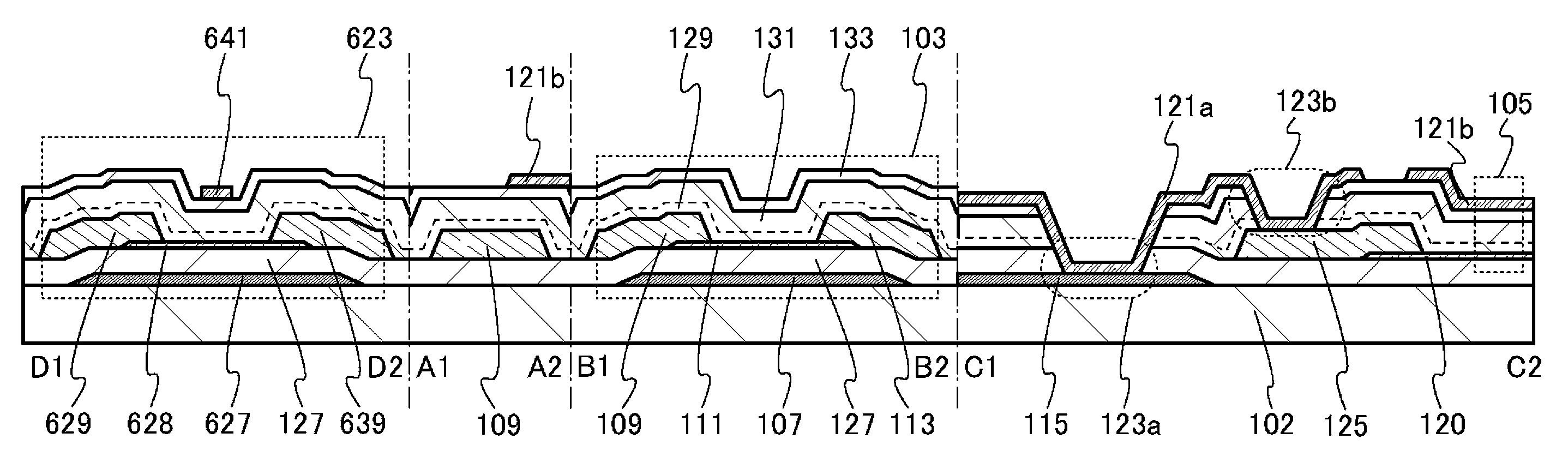
다음에, 도 2의 일점 쇄선 A1-A2 간, 일점 쇄선 B1-B2 간, 일점 쇄선 C1-C2 간, 및 주사선 구동 회로(104)(도 1의 (A) 참조)에 제공되는 트랜지스터의 단면도를 도 3에 도시하였다. 여기서는 주사선 구동 회로(104)의 상면도를 생략함과 함께, 주사선 구동 회로(104)의 단면도를 D1-D2에 도시하였다. 또한, 여기에서는 주사선 구동 회로(104)에 제공되는 트랜지스터의 단면도를 도시하였지만, 이 트랜지스터는 신호선 구동 회로(106)에 제공할 수도 있다.Next, a cross-sectional view of a transistor provided in the dashed-dotted line A1-A2, the dashed-dotted line B1-B2, the dashed-dotted line C1-C2, and the scanning line driving circuit 104 (refer to FIG. 1A) of FIG. It is shown in Figure 3. Here, a top view of the scanning
먼저, 화소(101)의 일점 쇄선 A1-A2 간, 일점 쇄선 B1-B2 간, 및 일점 쇄선 C1-C2 간의 구조에 대하여 설명한다. 기판(102) 위에, 트랜지스터(103)의 게이트 전극을 포함하는 주사선(107)이 제공되고, 주사선(107)과 같은 표면 위에 용량선(115)이 제공된다. 주사선(107) 및 용량선(115) 위에 게이트 절연막(127)이 제공된다. 게이트 절연막(127) 중 주사선(107)과 중첩되는 영역 위에 반도체막(111)이 제공되고, 게이트 절연막(127) 위에 도전막(120)이 제공된다. 반도체막(111) 위, 및 게이트 절연막(127) 위에 트랜지스터(103)의 소스 전극을 포함하는 신호선(109)과, 트랜지스터(103)의 드레인 전극을 포함하는 도전막(113)이 제공된다. 도전막(120) 위에 도전막(125)이 제공된다. 게이트 절연막(127) 위, 신호선(109) 위, 반도체막(111) 위, 도전막(113) 위, 도전막(125) 위, 도전막(120) 위에 트랜지스터(103)의 보호 절연막으로서 기능하는 절연막(129), 절연막(131), 및 절연막(133)이 제공된다. 게이트 절연막(127), 절연막(129), 절연막(131), 및 절연막(133)에는 용량선(115)에 도달되는 개구(123a)가 제공되고, 또한, 절연막(129), 절연막(131), 및 절연막(133)에는 도전막(125)에 도달되는 개구(123b)가 제공되고, 개구(123a), 개구(123b), 용량선(115) 위, 도전막(125) 위, 및 절연막(133) 위에 전극(121a)이 제공된다. 절연막(129), 절연막(131), 및 절연막(133)에는 도전막(113)에 도달되는 개구(117)(도 2 참조)가 제공되고 개구(117) 및 절연막(133) 위에 화소 전극(121b)이 제공된다.First, a structure between the dashed-dotted line A1-A2, the dashed-dotted line B1-B2, and the dashed-dotted line C1-C2 of the
본 실시형태에 기재되는 용량 소자(105)는 한 쌍의 전극 중 한쪽 전극이 반도체막(111)과 같게 형성된, 도전율을 증대시킨 도전막(120)이고, 한 쌍의 전극 중 다른 한쪽 전극이 화소 전극(121b)이고, 한 쌍의 전극 사이에 제공된 유전체막이 절연막(129), 절연막(131), 및 절연막(133)이다.The
다음에, 주사선 구동 회로(104)에 제공되는 트랜지스터의 구조에 대하여 설명한다. 기판(102) 위에 트랜지스터(623)의 게이트 전극(627)이 제공된다. 게이트 전극(627) 위에 게이트 절연막(127)이 제공된다. 게이트 절연막(127) 중 게이트 전극(627)과 중첩되는 영역 위에 반도체막(628)이 제공된다. 반도체막(628) 위, 및 게이트 절연막(127) 위에 트랜지스터(623)의 소스 전극(629) 및 드레인 전극(639)이 제공된다. 게이트 절연막(127) 위, 소스 전극(629) 위, 반도체막(628) 위, 및 드레인 전극(639) 위에, 트랜지스터(623)의 보호 절연막으로서 기능하는 절연막(129), 절연막(131), 및 절연막(133)이 제공된다. 절연막(133) 위에는 도전막(641)이 제공된다.Next, the structure of a transistor provided in the scanning
또한, 기판(102)과, 주사선(107), 용량선(115), 게이트 전극(627), 및 게이트 절연막(127)과의 사이에는 하지 절연막이 제공되어도 좋다.Further, a base insulating film may be provided between the
트랜지스터(623)에서, 반도체막(628)을 개재하여, 게이트 전극(627)과 중첩되는 도전막(641)을 제공함으로써, 상이한 드레인 전압에서, 온 전류의 상승 게이트 전압의 편차를 저감시킬 수 있다. 또한, 도전막(641)과 대향하는 반도체막(628)의 면에서, 소스 전극(629)과 드레인 전극(639) 사이에 흐르는 전류를 제어할 수 있고, 상이한 트랜지스터에서의 전기 특성의 편차를 저감시킬 수 있다. 또한, 도전막(641)을 제공함으로써, 주위의 전계의 변화가 반도체막(628)에 미치는 영향을 경감하고, 트랜지스터의 신뢰성을 향상시킬 수 있다. 또한, 도전막(641)의 전위를 구동 회로의 최저 전위(Vss, 예를 들어, 소스 전극(629)의 전위를 기준으로 하는 경우, 소스 전극(629)의 전위)와 동일한 전위 또는 이와 동등 전위로 함으로써, 트랜지스터의 문턱 전압의 변동을 저감시킬 수 있고, 트랜지스터의 신뢰성을 높일 수 있다. 다만, 경우에 따라서 또는 상황에 따라서 도전막(641)을 제공하지 않을 수도 있다.In the
절연막(129) 및 절연막(131)은 예를 들어 산화 실리콘, 산화 질화 실리콘, 산화 알루미늄, 산화 하프늄, 산화 갈륨, 또는 Ga-Zn계 금속 산화물 등의 산화 절연 재료를 사용한 단층 구조 또는 적층 구조로 제공할 수 있다.The insulating
절연막(129)의 두께는 5nm 이상 150nm 이하, 바람직하게는 5nm 이상 50nm 이하, 더 바람직하게는 10nm 이상 30nm 이하로 할 수 있다. 절연막(131)의 두께는 30nm 이상 500nm 이하, 바람직하게는 150nm 이상 400nm 이하로 할 수 있다.The thickness of the insulating
또한, 절연막(133)은 예를 들어, 질화 산화 실리콘, 질화 실리콘, 질화 알루미늄, 질화 산화 알루미늄 등의 질화 절연 재료를 사용한 단층 구조 또는 적층 구조로 제공할 수 있다.In addition, the insulating
절연막(133)으로서 수소 함유량이 적은 질화 절연막을 제공하여도 좋다. 상기 질화 절연막으로서는 예를 들어, 승온 이탈 가스 분석(이하, TDS 분석이라고 함)에 의하여 측정되는, 표면 온도가 100℃ 이상 700℃ 이하, 바람직하게는 100℃ 이상 500℃ 이하의 가열 처리에서의 수소 분자의 방출량이 5.0×10²¹분자/cm3 미만이며, 바람직하게는 3.0×10²¹분자/cm3 미만이고, 더 바람직하게는 1.0×10²¹분자/cm3 미만인 질화 절연막이다.As the insulating
절연막(133)은 외부로부터 수소나 물 등의 불순물이 침입하는 것을 억제하는 기능을 발휘할 수 있는 두께로 한다. 예를 들어, 50nm 이상 200nm 이하, 바람직하게는 50nm 이상 150nm 이하, 더 바람직하게는 50nm 이상 100nm 이하로 할 수 있다.The insulating
또한, 트랜지스터(103) 및 트랜지스터(623) 위에 질화 절연막인 절연막(133)을 제공함으로써, 상기 산화 실리콘막에 포함되는 탄소 등의 불순물이 절연막(133)에 의하여 블로킹되어, 트랜지스터(103)의 반도체막(111) 및 트랜지스터(623)의 반도체막(628)으로 불순물이 이동하는 것을 저감할 수 있기 때문에, 트랜지스터의 전기 특성의 편차를 저감할 수 있다.In addition, by providing an insulating
또한, 절연막(129) 및 절연막(131)의 한쪽 또는 양쪽은 화학양론적 조성을 만족시키는 산소보다 많은 산소를 포함하는 산화 절연막인 것이 바람직하다. 이와 같이 함으로써, 상기 산화물 반도체막으로부터의 산소의 이탈을 방지함과 함께, 산소 과잉 영역에 포함되는 상기 산소를 산화물 반도체막으로 이동시켜 산소 결손을 보전할 수 있다. 예를 들어, TDS 분석에 의하여 측정되는, 표면 온도가 100℃ 이상 700℃ 이하, 바람직하게는 100℃ 이상 500℃ 이하의 가열 처리에서의 산소 분자의 방출량이 1.0×10¹⁸분자/cm3 이상인 산화 절연막을 사용함으로써, 상기 산화물 반도체막에 포함되는 산소 결손을 보전할 수 있다. 또한, 절연막(129) 및 절연막(131)의 한쪽 또는 양쪽에서, 화학양론적 조성보다 과잉으로 산소를 포함하는 영역(산소 과잉 영역)이 부분적으로 존재하는 산화 절연막이라도 좋고, 적어도 반도체막(111)과 중첩되는 영역에 산소 과잉 영역이 존재함으로써, 상기 산화물 반도체막으로부터의 산소의 이탈을 방지함과 함께, 산소 과잉 영역에 포함되는 상기 산소를 산화물 반도체막으로 이동시켜 산소 결손을 보전할 수 있다.In addition, it is preferable that one or both of the insulating
절연막(131)이 화학양론적 조성을 만족시키는 산소보다 많은 산소를 포함하는 산화 절연막인 경우, 절연막(129)은 산소를 투과하는 산화 절연막으로 하는 것이 바람직하다. 또한, 절연막(129)에서, 외부로부터 절연막(129)으로 들어온 산소는 모두 절연막(129)을 통과하여 이동하지 않고, 절연막(129)에 머무르는 산소도 있다. 또한, 미리 절연막(129)에 포함되고, 절연막(129)으로부터 외부로 이동하는 산소도 있다. 따라서, 절연막(129)은 산소의 확산 계수가 큰 산화 절연막인 것이 바람직하다.When the insulating
또한, 절연막(129)은 반도체막(111) 및 반도체막(628)인 산화물 반도체막과 접하기 때문에 산소를 투과시킬 뿐만 아니라, 반도체막(111)과의 계면 준위 밀도를 낮게 하는 산화 절연막인 것이 바람직하다. 예를 들어, 절연막(129)은 절연막(131)보다 막 중의 결함 밀도가 낮은 산화 절연막인 것이 바람직하다. 구체적으로는 전자 스핀 공명 측정에 의하여 얻어지는 g값=2.001(E'-center)의 스핀 밀도가 3.0×10¹⁷spins/cm3 이하, 바람직하게는 5.0×10¹⁶spins/cm3 이하의 산화 절연막이다. 또한, 전자 스핀 공명 측정에 의하여 얻어지는 g값=2.001의 스핀 밀도는 절연막(129)에 포함되는 댕글링 본드의 존재량에 대응한다.In addition, since the insulating
또한, 절연막(129) 및 절연막(131)의 한쪽 또는 양쪽이 질소에 대한 배리어성을 갖는 절연막인 것이 바람직하다. 예를 들어, 치밀한 산화 절연막으로 함으로써 질소에 대한 배리어성을 가질 수 있고, 구체적으로는 25℃에서 0.5 중량%의 불산을 사용한 경우의 에칭 속도가 10nm/분 이하인 산화 절연막으로 하는 것이 바람직하다.In addition, it is preferable that one or both of the insulating
또한, 절연막(129) 및 절연막(131)의 한쪽 또는 양쪽을, 산화 질화 실리콘 또는 질화 산화 실리콘 등 질소를 포함하는 산화 절연막으로 하는 경우, SIMS에 의하여 얻어지는 질소 농도는 SIMS 검출 하한 이상 3×10²⁰atoms/cm3 미만, 바람직하게는 1×10¹⁸atoms/cm3 이상 1×10²⁰atoms/cm3 이하로 한다. 이와 같이 함으로써, 트랜지스터(103)에 포함되는 반도체막(111)으로의 질소의 이동량을 줄일 수 있다. 또한, 이와 같이 함으로써, 질소를 포함하는 산화 절연막 자체의 결함량을 줄일 수 있다.In addition, when one or both of the insulating
이하에, 상기 구조의 구성 요소에 대하여 자세히 기재한다.Hereinafter, the constituent elements of the structure will be described in detail.
기판(102)의 재질 등에 큰 제한은 없지만, 적어도 반도체 장치의 제작 공정에서 수행하는 가열 처리에 견딜 수 있을 정도의 내열성을 가질 필요가 있다. 예를 들어, 유리 기판, 세라믹 기판, 플라스틱 기판 등이 있고, 유리 기판으로서는 바륨 보로실리케이트 유리, 알루미노 보로실리케이트 유리, 또는 알루미노실리케이트 유리 등의 무알칼리 유리 기판을 사용하면 좋다. 또한, 스테인리스 스틸 합금 등 투광성을 갖지 않는 기판을 사용할 수도 있다. 이 경우에는 기판 표면에 절연막을 제공하는 것이 바람직하다. 또한, 기판(102)으로서 석영 기판, 사파이어 기판, 단결정 반도체 기판, 다결정 반도체 기판, 화합물 반도체 기판, SOI(Silicon On Insulator) 기판 등을 사용할 수도 있다.Although there is no great limitation on the material of the
주사선(107), 용량선(115), 및 게이트 전극(627)은 대전류를 흘리기 때문에, 금속막으로 형성되는 것이 바람직하고, 대표적으로는 몰리브데넘(Mo), 티타늄(Ti), 텅스텐(W) 탄탈럼(Ta), 알루미늄(Al), 구리(Cu), 크로뮴(Cr), 네오디뮴(Nd), 스칸듐(Sc) 등의 금속 재료 또는 이들을 주성분으로 하는 합금 재료를 사용한 단층 구조 또는 적층 구조로 제공한다.Since the
주사선(107), 용량선(115), 및 게이트 전극(627)의 일례로서는 실리콘을 포함하는 알루미늄을 사용한 단층 구조, 알루미늄 위에 티타늄을 적층하는 2층 구조, 질화 티타늄 위에 티타늄을 적층하는 2층 구조, 질화 티타늄 위에 텅스텐을 적층하는 2층 구조, 질화 탄탈럼 위에 텅스텐을 적층하는 2층 구조, 구리-마그네슘-알루미늄 합금 위에 구리를 적층하는 2층 구조, 질화 티타늄 위에 구리를 적층하고, 이들 위에 텅스텐을 더 형성하는 3층 구조 등이 있다.Examples of the
또한, 주사선(107), 용량선(115), 및 게이트 전극(627)의 재료로서 화소 전극(121b)에 적용할 수 있는 투광성을 갖는 도전성 재료를 사용할 수 있다.In addition, a light-transmitting conductive material applicable to the
또한, 주사선(107), 용량선(115), 및 게이트 전극(627)의 재료로서 질소를 포함하는 금속 산화물, 구체적으로는 질소를 포함하는 In-Ga-Zn계 산화물이나, 질소를 포함하는 In-Sn계 산화물이나, 질소를 포함하는 In-Ga계 산화물이나, 질소를 포함하는 In-Zn계 산화물이나, 질소를 포함하는 Sn계 산화물이나, 질소를 포함하는 In계 산화물이나, 금속 질화막(InN, SnN 등)을 사용할 수 있다. 이들 재료는 5eV(전자 볼트) 이상의 일함수를 갖는다. 트랜지스터(103)의 반도체막(111)으로서 산화물 반도체를 사용하는 경우, 주사선(107)(트랜지스터(103)의 게이트 전극)으로서 질소를 포함하는 금속 산화물을 사용함으로써, 트랜지스터(103)의 문턱 전압을 플러스 방향으로 변동시킬 수 있어, 소위 노멀리 오프 특성을 갖는 트랜지스터를 구현할 수 있다. 예를 들어, 질소를 포함하는 In-Ga-Zn계 산화물을 사용하는 경우, 적어도 반도체막(111)인 산화물 반도체막보다 높은 질소 농도, 구체적으로는 질소 농도가 7atoms% 이상인 In-Ga-Zn계 산화물을 사용할 수 있다.In addition, a metal oxide containing nitrogen as a material of the
주사선(107), 용량선(115), 및 게이트 전극(627)에서, 저저항 재료인 알루미늄이나 구리를 사용하는 것이 바람직하다. 알루미늄이나 구리를 사용함으로써, 신호 지연을 저감하고, 표시 품질을 높일 수 있다. 또한, 알루미늄은 내열성이 낮고, 힐록, 위스커, 또는 마이그레이션(migration)으로 인한 불량이 발생하기 쉽다. 알루미늄의 마이그레이션을 막기 위하여, 알루미늄에 몰리브데넘, 티타늄, 텅스텐 등의 알루미늄보다 융점이 높은 금속 재료를 적층하는 것이 바람직하다. 또한, 구리를 사용하는 경우에도, 마이그레이션으로 인한 불량이나 구리 원소의 확산을 막기 위하여, 구리에 몰리브데넘, 티타늄, 텅스텐 등의 구리보다 융점이 높은 금속 재료를 적층하는 것이 바람직하다.For the
게이트 절연막(127)은 예를 들어, 산화 실리콘, 산화 질화 실리콘, 질화 산화 실리콘, 질화 실리콘, 산화 알루미늄, 산화 하프늄, 산화 갈륨, 또는 Ga-Zn계 금속 산화물 등의 절연 재료를 사용한 단층 구조 또는 적층 구조로 제공한다. 또한, 반도체막(111)인 산화물 반도체막과의 계면 특성을 향상시키기 위하여, 게이트 절연막(127)에서 적어도 반도체막(111)과 접하는 영역은 산화 절연막으로 형성되는 것이 바람직하다.The
또한, 게이트 절연막(127)에, 산소, 수소, 물 등에 대한 배리어성을 갖는 절연막을 제공함으로써, 반도체막(111)인 산화물 반도체막으로부터 외부로 산소가 확산되거나 외부로부터 이 산화물 반도체막으로 수소, 물 등이 침입하는 것을 막을 수 있다. 산소, 수소, 물 등에 대한 배리어성을 갖는 절연막으로서는, 산화 알루미늄막, 산화 질화 알루미늄막, 산화 갈륨막, 산화 질화 갈륨막, 산화 이트륨막, 산화 질화 이트륨막, 산화 하프늄막, 산화 질화 하프늄막, 질화 실리콘막 등이 있다.In addition, by providing the
또한, 게이트 절연막(127)으로서, 하프늄 실리케이트(HfSixOy), 질소를 갖는 하프늄 실리케이트(HfSixOy), 질소를 갖는 하프늄 알루미네이트(HfAlxOy), 산화 하프늄, 산화 이트륨 등의 high-k 재료를 사용함으로써 트랜지스터(103)의 게이트 누설을 저감시킬 수 있다.In addition, as the
또한, 게이트 절연막(127)은 이하의 적층 구조로 하는 것이 바람직하다. 제 1 질화 실리콘막으로서 결함량이 적은 질화 실리콘막을 제공하고, 제 1 질화 실리콘막 위에 제 2 질화 실리콘막으로서 수소 이탈량 및 암모니아 이탈량이 적은 질화 실리콘막을 제공하고, 제 2 질화 실리콘막 위에 상술한 게이트 절연막(127)에 대한 기재에서 나열한 산화 절연막 중 어느 것을 제공하는 것이 바람직하다.In addition, it is preferable that the
제 2 질화 실리콘막으로서는 승온 이탈 가스 분석법에서, 수소 분자의 이탈량이 5×10²¹분자/cm3 미만, 바람직하게는 3×10²¹분자/cm3 이하, 더욱 바람직하게는 1×10²¹분자/cm3 이하이며, 암모니아 분자의 이탈량이 1×10²²분자/cm3 미만, 바람직하게는 5×10²¹분자/cm3 이하, 더 바람직하게는 1×10²¹분자/cm3 이하인 질화 절연막을 사용하는 것이 바람직하다. 상기 제 1 질화 실리콘막 및 제 2 질화 실리콘막을 게이트 절연막(127)의 일부로서 사용함으로써, 게이트 절연막(127)으로서 결함량이 적고, 또한 수소 이탈량 및 암모니아 이탈량이 적은 게이트 절연막을 형성할 수 있다. 이 결과, 게이트 절연막(127)에 포함되는 수소 및 질소가 반도체막(111)으로 이동하는 양을 저감할 수 있다.As the second silicon nitride film, in the elevated temperature release gas analysis method, the amount of desorbed hydrogen molecules is less than 5×10 21 molecules/cm 3 , preferably 3×10 21 molecules/cm 3 or less, more preferably 1×10 21 molecules/ cm 3 or less, and the amount of ammonia molecules desorbed is less than 1×10 22 molecules/cm 3 , preferably 5×10 21 molecules/cm 3 or less, more preferably 1×10 21 molecules/cm 3 or less. It is desirable to do. By using the first silicon nitride film and the second silicon nitride film as part of the
산화물 반도체를 사용한 트랜지스터에서, 산화물 반도체막 및 게이트 절연막의 계면, 또는 게이트 절연막에 포획 준위(계면 준위라고도 함)가 존재하면, 트랜지스터의 문턱 전압의 변동, 대표적으로는 문턱 전압의 마이너스 방향으로의 변동, 및 트랜지스터가 온 상태가 될 때에 드레인 전류가 한 자릿수 변화하는 데 필요한 게이트 전압을 나타내는 서브스레시홀드 계수(S값)가 증대되는 원인이 된다. 이 결과, 트랜지스터마다 전기 특성이 흩어진다는 문제가 있다. 그러므로, 게이트 절연막으로서 결함량이 적은 질화 실리콘막을 사용함으로써, 또한, 반도체막(111)과 접하는 영역에 산화 절연막을 제공함으로써, 문턱 전압의 마이너스 시프트를 저감함과 함께, S값의 증대를 억제할 수 있다.In a transistor using an oxide semiconductor, when a trapping level (also referred to as an interface level) exists at the interface between the oxide semiconductor film and the gate insulating film, or at the gate insulating film, the threshold voltage of the transistor fluctuates, typically, the threshold voltage fluctuates in the negative direction. , And the subthreshold coefficient (S value) representing the gate voltage required to change the drain current by one digit when the transistor is turned on is caused to increase. As a result, there is a problem that electrical characteristics are scattered for each transistor. Therefore, by using a silicon nitride film with a small amount of defects as the gate insulating film, and by providing an oxide insulating film in a region in contact with the
게이트 절연막(127)의 두께는 5nm 이상 400nm 이하, 더 바람직하게는 10nm 이상 300nm 이하, 더욱 바람직하게는 50nm 이상 250nm 이하로 하면 좋다.The thickness of the
반도체막(111) 및 반도체막(628)은 산화물 반도체막이고, 이 산화물 반도체막은 비정질 구조, 단결정 구조, 또는 다결정 구조로 할 수 있다. 또한, 도전막(120)도 산화물 반도체막의 도전율을 증대시켜 형성된다. 또한, 반도체막(111)의 두께는 1nm 이상 100nm 이하, 바람직하게는 1nm 이상 50nm 이하, 더 바람직하게는 1nm 이상 30nm 이하, 더욱 바람직하게는 3nm 이상 20nm 이하로 한다.The
반도체막(111) 및 반도체막(628)에 적용할 수 있는 산화물 반도체로서는, 에너지 갭이 2eV 이상, 바람직하게는 2.5eV 이상, 더 바람직하게는 3eV 이상인 것이다. 이와 같이, 에너지 갭이 넓은 산화물 반도체를 사용함으로써, 트랜지스터(103)의 오프 전류를 저감시킬 수 있다.As an oxide semiconductor applicable to the
반도체막(111) 및 반도체막(628)에 적용할 수 있는 산화물 반도체로서는, 적어도 인듐(In) 또는 아연(Zn)을 포함하는 것이 바람직하다. 또는 In과 Zn의 양쪽 모두를 포함하는 것이 바람직하다. 또한, 이 산화물 반도체를 사용한 트랜지스터의 전기 특성의 편차를 줄이기 위하여, 이들에 더하여, 스테빌라이저(stabilizer)의 하나 또는 복수를 갖는 것이 바람직하다.As an oxide semiconductor applicable to the
스테빌라이저로서는 갈륨(Ga), 주석(Sn), 하프늄(Hf), 알루미늄(Al), 또는 지르코늄(Zr) 등이 있다. 또한, 다른 스테빌라이저로서는 란타노이드인 란타넘(La), 세륨(Ce), 프라세오디뮴(Pr), 네오디뮴(Nd), 사마륨(Sm), 유로퓸(Eu), 가돌리늄(Gd), 테르븀(Tb), 디스프로슘(Dy), 홀뮴(Ho), 에르븀(Er), 툴륨(Tm), 이테르븀(Yb), 루테튬(Lu) 등이 있다.Examples of stabilizers include gallium (Ga), tin (Sn), hafnium (Hf), aluminum (Al), or zirconium (Zr). In addition, other stabilizers include lanthanides such as lanthanum (La), cerium (Ce), praseodymium (Pr), neodymium (Nd), samarium (Sm), europium (Eu), gadolinium (Gd), terbium (Tb), There are dysprosium (Dy), holmium (Ho), erbium (Er), thulium (Tm), ytterbium (Yb), lutetium (Lu), and the like.
반도체막(111) 및 반도체막(628)에 적용할 수 있는 산화물 반도체로서는, 예를 들어, 산화 인듐, 산화 주석, 산화 아연, 2종류의 금속을 포함하는 산화물인 In-Zn계 산화물, Sn-Zn계 산화물, Al-Zn계 산화물, Zn-Mg계 산화물, Sn-Mg계 산화물, In-Mg계 산화물, In-Ga계 산화물, 3종류의 금속을 포함하는 산화물인 In-Ga-Zn계 산화물, In-Al-Zn계 산화물, In-Sn-Zn계 산화물, Sn-Ga-Zn계 산화물, Al-Ga-Zn계 산화물, Sn-Al-Zn계 산화물, In-Hf-Zn계 산화물, In-Zr-Zn계 산화물, In-Ti-Zn계 산화물, In-Sc-Zn계 산화물, In-Y-Zn계 산화물, In-La-Zn계 산화물, In-Ce-Zn계 산화물, In-Pr-Zn계 산화물, In-Nd-Zn계 산화물, In-Sm-Zn계 산화물, In-Eu-Zn계 산화물, In-Gd-Zn계 산화물, In-Tb-Zn계 산화물, In-Dy-Zn계 산화물, In-Ho-Zn계 산화물, In-Er-Zn계 산화물, In-Tm-Zn계 산화물, In-Yb-Zn계 산화물, In-Lu-Zn계 산화물, 4종류의 금속을 포함하는 산화물인 In-Sn-Ga-Zn계 산화물, In-Hf-Ga-Zn계 산화물, In-Al-Ga-Zn계 산화물, In-Sn-Al-Zn계 산화물, In-Sn-Hf-Zn계 산화물, In-Hf-Al-Zn계 산화물을 사용할 수 있다.Examples of oxide semiconductors that can be applied to the
여기서, In-Ga-Zn계 산화물이란, In과 Ga과 Zn을 주성분으로서 갖는 산화물이라는 의미이며, In과 Ga과 Zn의 비율은 불문한다. 또한, In과 Ga과 Zn 외의 금속 원소가 들어가도 좋다.Here, the In-Ga-Zn-based oxide means an oxide having In, Ga, and Zn as main components, and the ratio of In, Ga, and Zn is irrelevant. Further, metal elements other than In, Ga, and Zn may be included.
또한, 산화물 반도체로서 InMO3(ZnO)m(m>0)으로 표기되는 재료를 사용하여도 좋다. 또한, M은 Ga, Fe, Mn 및 Co로부터 선택된 하나의 금속 원소 또는 복수의 금속 원소, 또는 상술한 스테빌라이저로서의 원소를 나타낸다.Further, as the oxide semiconductor, a material represented by InMO 3 (ZnO) m (m>0) may be used. Further, M represents one metal element or a plurality of metal elements selected from Ga, Fe, Mn, and Co, or an element as the above-described stabilizer.
예를 들어, In:Ga:Zn=1:1:1, In:Ga:Zn=2:2:1, 또는 In:Ga:Zn=3:1:2의 원자수비의 In-Ga-Zn계 금속 산화물을 사용할 수 있다. 또는 In:Sn:Zn=1:1:1, In:Sn:Zn=2:1:3, 또는 In:Sn:Zn=2:1:5의 원자수비의 In-Sn-Zn계 금속 산화물을 사용하면 좋다. 또한, 금속 산화물의 원자수비는 오차로서 상술한 원자수비의 플러스마이너스20%의 변동을 포함한다.For example, In:Ga:Zn=1:1:1, In:Ga:Zn=2:2:1, or In:Ga:Zn=3:1:2 In-Ga-Zn system Metal oxides can be used. Or In:Sn:Zn=1:1:1, In:Sn:Zn=2:1:3, or In:Sn:Zn=2:1:5, an In-Sn-Zn-based metal oxide having an atomic ratio of Good to use. In addition, the atomic number ratio of the metal oxide includes a variation of plus or minus 20% of the atomic number ratio described above as an error.
그러나, 이들에 한정되지 않고, 필요로 하는 반도체 특성 및 전기 특성(전계 효과 이동도, 문턱 전압 등)에 따라 적절한 원자수비의 것을 사용하면 좋다. 또한, 필요로 하는 반도체 특성을 얻기 위하여, 캐리어 밀도나 불순물 농도, 결함 밀도, 금속 원소와 산소의 원자수비, 원자간 거리, 밀도 등을 적절한 것으로 하는 것이 바람직하다. 예를 들어, In-Sn-Zn계 산화물에서는 비교적 쉽게 높은 전계 효과 이동도를 얻을 수 있다. 그러나, In-Ga-Zn계 산화물에서도, 벌크 내 결함 밀도를 낮게 함으로써, 전계 효과 이동도를 높일 수 있다.However, the present invention is not limited to these, and a material having an appropriate atomic number ratio may be used depending on the required semiconductor properties and electrical properties (field effect mobility, threshold voltage, etc.). In addition, in order to obtain required semiconductor properties, it is preferable to appropriately set the carrier density, impurity concentration, defect density, atomic number ratio of metal element and oxygen, interatomic distance, density, and the like. For example, in an In-Sn-Zn-based oxide, a high field effect mobility can be obtained relatively easily. However, even in the In-Ga-Zn-based oxide, the field effect mobility can be increased by lowering the defect density in the bulk.
트랜지스터(103)의 소스 전극을 포함하는 신호선(109), 트랜지스터(103)의 드레인 전극을 포함하는 도전막(113), 및 용량 소자(105)의 도전막(120)과 용량선(115)을 전기적으로 접속하는 도전막(125), 및 소스 전극(629) 및 드레인 전극(639)은 주사선(107), 용량선(115), 및 게이트 전극(627)에 적용할 수 있는 재료를 사용한 단층 구조 또는 적층 구조로 제공한다.The
전극(121a), 화소 전극(121b), 및 도전막(641)은 인듐 주석 산화물, 산화 텅스텐을 포함하는 인듐 산화물, 산화 텅스텐을 포함하는 인듐 아연 산화물, 산화 티타늄을 포함하는 인듐 산화물, 산화 티타늄을 포함하는 인듐 주석 산화물, 인듐 아연 산화물, 산화 실리콘을 첨가한 인듐 주석 산화물 등의 투광성을 갖는 도전성 재료로 형성된다.The
여기서, 본 실시형태에 기재되는 화소(101)에 포함되는 각 구성 요소의 접속에 대하여, 도 1의 (C)에 도시된 회로도 및 도 3에 도시된 단면도를 사용하여 설명한다.Here, the connection of each constituent element included in the
도 1의 (C)는 도 1의 (A)에 도시된 반도체 장치가 갖는 화소(101)의 자세한 회로도의 일례다. 도 1의 (C) 및 도 3에 도시된 바와 같이, 트랜지스터(103)는 게이트 전극을 포함하는 주사선(107)과, 소스 전극을 포함하는 신호선(109)과, 드레인 전극을 포함하는 도전막(113)을 갖는다.FIG. 1C is an example of a detailed circuit diagram of a
용량 소자(105)에서, 전극(121a) 및 도전막(125)을 통하여 용량선(115)과 접속되는 도전막(120)이 한쪽 전극으로서 기능한다. 또한, 드레인 전극을 포함하는 도전막(113)과 접속되는 화소 전극(121b)이 다른 한쪽 전극으로서 기능한다. 또한, 도전막(120)과 화소 전극(121b) 사이에 제공되는 절연막(129), 절연막(131), 및 절연막(133)이 유전체막으로서 기능한다.In the
액정 소자(108)는, 화소 전극(121b), 대향 전극(154), 및 화소 전극(121b)과 대향 전극(154) 사이에 제공되는 액정층으로 구성된다.The
용량 소자(105)에서, 도전막(120)은 반도체막(111)과 동일한 구성에 도펀트를 첨가한 구성이고, 용량 소자(105)의 전극으로서 기능한다. 왜냐하면, 화소 전극(121b)을 게이트 전극으로서 기능시킬 수 있고, 절연막(129), 절연막(131) 및 절연막(133)을 게이트 절연막으로서 기능시킬 수 있고, 용량선(115)을 소스 전극 또는 드레인 전극으로서 기능시킬 수 있고, 결과적으로 용량 소자(105)를 트랜지스터와 마찬가지로 동작시키고, 도전막(120)을 도통 상태로 할 수 있기 때문이다. 즉, 용량 소자(105)를 MOS(Metal Oxide Semiconductor) 커패시터로 할 수 있다. MOS 커패시터는 문턱 전압(Vth)보다 높은 전압이, MOS 커패시터를 구성하는 전극의 한쪽(용량 소자(105)에서는 화소 전극(121b))에 인가되면 충전된다. 또한, 용량선(115)에 인가하는 전위를 제어함으로써 도전막(120)을 도통 상태로 하고, 도전막(120)을 용량 소자의 한쪽 전극으로서 기능시킬 수 있다. 이 경우, 용량선(115)에 인가하는 전위를 이하와 같이 한다. 화소 전극(121b)의 전위는 액정 소자(108)(도 1의 (C) 참조)를 동작시키기 위하여, 비디오 신호의 중심 전위를 기준으로 하여 플러스 방향 및 마이너스 방향으로 변동한다. 용량 소자(105)(MOS 커패시터)를 항상 도통 상태로 해 두기 위해서는 용량선(115)의 전위를 항상 화소 전극(121b)에 인가하는 전위보다 용량 소자(105)(MOS 커패시터)의 문턱 전압분 이상 낮게 해 둘 필요가 있다. 다만, 용량 소자(105)에서, 한쪽 전극으로서 기능하는 도전막(120)은 n형이며, 도전율이 높기 때문에, 문턱 전압이 마이너스 방향으로 시프트된다. 도전막(120)의 전위(바꿔 말하면, 용량선(115)의 전위)는 용량 소자(105)의 문턱 전압이 마이너스 방향으로 시프트되는 양에 따라, 화소 전극(121b)이 취할 수 있는 가장 낮은 전위로부터 높게 해 나갈 수 있다. 따라서, 용량 소자(105)의 문턱 전압이 큰 음의 값을 나타내는 경우, 용량선(115)의 전위는 화소 전극(121b)의 전위보다 높게 할 수 있다. 이와 같이 함으로써, 도전막(120)을 항상 도통 상태로 할 수 있고, 용량 소자(105)(MOS 커패시터)를 도통 상태로 할 수 있다.In the
또한, 반도체막(111) 및 반도체막(628) 위에 제공되는 절연막(129)을, 산소를 투과시킴과 함께, 반도체막(111) 및 반도체막(628)과의 계면 준위 밀도를 낮게 하는 산화 절연막으로 하고, 절연막(131)을, 산소 과잉 영역을 포함하는 산화 절연막 또는 화학양론적 조성을 만족시키는 산소보다 많은 산소를 포함하는 산화 절연막으로 함으로써, 반도체막(111) 및 반도체막(628)인 산화물 반도체막으로 산소를 공급하기 쉬워지고, 이 산화물 반도체막으로부터 산소가 이탈되는 것을 방지할 수 있음과 함께, 절연막(131)에 포함되는 이 산소를 산화물 반도체막으로 이동시켜, 산화물 반도체막에 포함되는 산소 결손을 보전할 수 있다. 이 결과, 트랜지스터(103)가 노멀리 온 특성이 되는 것을 억제할 수 있음과 함께, 용량 소자(105)(MOS 커패시터)가 항상 도통 상태가 되도록, 용량선(115)에 인가하는 전위를 제어할 수 있기 때문에, 반도체 장치의 전기 특성 및 신뢰성을 향상시킬 수 있다.In addition, the insulating
또한, 절연막(131) 위에 제공되는 절연막(133)으로서 질화 절연막을 사용함으로써, 외부로부터 수소나 물 등의 불순물이 반도체막(111) 및 도전막(120)에 침입하는 것을 억제할 수 있다. 또한, 절연막(133)으로서 수소 함유량이 적은 질화 절연막을 제공함으로써, 트랜지스터(103) 및 용량 소자(105)(MOS 커패시터)의 전기 특성이 변동되는 것을 억제할 수 있다.Further, by using a nitride insulating film as the insulating
또한, 화소(101) 내에 용량 소자(105)를 크게(대면적으로) 형성할 수 있다. 따라서, 개구율을 높이면서, 전하 용량을 증대시킨 반도체 장치를 얻을 수 있다. 이 결과, 표시 품질이 뛰어난 반도체 장치를 얻을 수 있다.In addition, the
<반도체 장치의 제작 방법><Method of manufacturing semiconductor device>
다음에, 상술한 반도체 장치에 나타내는 기판(102) 위에 제공된 소자부의 제작 방법에 대하여, 도 4 및 도 5를 사용하여 설명한다.Next, a method of fabricating the element portion provided on the
먼저, 기판(102) 위에 주사선(107), 용량선(115), 및 게이트 전극(627)을 형성하고, 주사선(107), 용량선(115), 및 게이트 전극(627)을 덮도록 나중에 게이트 절연막(127)으로 가공되는 절연막(126)을 형성하고, 절연막(126) 중 주사선(107)과 중첩되는 영역 위에 반도체막(111)을 형성하고, 나중에 화소 전극(121b)이 형성되는 영역과 중첩되도록 반도체막(119)을 형성한다. 또한, 게이트 전극(627)과 중첩되는 영역에 반도체막(628)을 형성한다(도 4의 (A) 참조).First, the
주사선(107), 용량선(115), 및 게이트 전극(627)은 상술한 재료를 사용하여 도전막을 형성하고, 이 도전막 위에 마스크를 형성하고, 이 마스크를 사용하여 가공함으로써 형성할 수 있다. 상기 도전막은 증착법, CVD법, 스퍼터링법, 스핀 코팅법 등 각종 성막 방법을 사용할 수 있다. 또한, 상기 도전막의 두께는 특별히 한정되지 않고, 형성하는 시간이나 원하는 저항률 등을 고려하여 결정할 수 있다. 상기 마스크는 예를 들어, 포토리소그래피 공정에 의하여 형성한 레지스트 마스크로 할 수 있다. 또한, 상기 도전막의 가공은 드라이 에칭 및 웨트 에칭의 한쪽 또는 양쪽에 의하여 수행될 수 있다.The
절연막(126)은 게이트 절연막(127)에 적용할 수 있는 재료를 사용하여, CVD법 또는 스퍼터링법 등 각종 성막 방법을 사용하여 형성할 수 있다.The insulating
또한, 게이트 절연막(127)에 산화 갈륨을 적용하는 경우는 MOCVD(Metal Organic Chemical Vapor Deposition)법을 사용하여 절연막(126)을 형성할 수 있다.In addition, when gallium oxide is applied to the
반도체막(111), 반도체막(119), 및 반도체막(628)은 상술한 산화물 반도체를 사용하여 산화물 반도체막을 형성하고, 이 산화물 반도체막 위에 마스크를 형성하고, 이 마스크를 사용하여 가공함으로써 형성할 수 있다. 상기 산화물 반도체막은 스퍼터링법, 도포법, 펄스 레이저 증착법, 레이저 어블레이션법(laser ablation method) 등을 사용하여 형성할 수 있다. 또한, 인쇄법을 사용함으로써, 소자 분리된 반도체막(111) 및 반도체막(119)을 절연막(126) 위에 직접 형성할 수 있다. 상기 산화물 반도체막을 스퍼터링법에 의하여 형성하는 경우, 플라즈마를 발생시키기 위한 전원 장치는 RF 전원 장치, AC 전원 장치, 또는 DC 전원 장치 등을 적절히 사용할 수 있다. 스퍼터링 가스는 희가스(대표적으로는 아르곤), 산소, 희가스 및 산소의 혼합 가스를 적절히 사용한다. 또한, 희가스 및 산소의 혼합 가스의 경우, 희가스에 대한 산소의 가스 비율을 높이는 것이 바람직하다. 또한, 타깃은 형성하는 산화물 반도체막의 조성에 맞추어, 적절히 선택하면 좋다. 또한, 상기 마스크는 예를 들어, 포토리소그래피 공정에 의하여 형성한 레지스트 마스크로 할 수 있다. 또한, 상기 산화물 반도체막의 가공은 드라이 에칭 및 웨트 에칭의 한쪽 또는 양쪽에 의하여 수행할 수 있다. 원하는 형상으로 에칭할 수 있도록, 재료에 따라 에칭 조건(에칭 가스나 에칭액, 에칭 시간, 온도 등)을 적절히 설정한다.The
반도체막(111), 반도체막(119), 및 반도체막(628)을 형성한 후에 가열 처리를 하고, 반도체막(111), 반도체막(119), 및 반도체막(628)인 산화물 반도체막의 탈수소화 또는 탈수화를 하는 것이 바람직하다. 상기 가열 처리의 온도는 대표적으로는 150℃ 이상 기판 변형점 미만, 바람직하게는 200℃ 이상 450℃ 이하, 더 바람직하게는 300℃ 이상 450℃ 이하로 한다. 또한, 반도체막(111) 및 반도체막(119)으로 가공하기 전의 산화물 반도체막에 상기 가열 처리를 수행하여도 좋다.After forming the
상기 가열 처리에서, 가열 처리 장치는 전기로에 한정되지 않고, 가열된 가스 등의 매체로부터의 열전도, 또는 열복사에 의하여, 피처리물을 가열하는 장치라도 좋다. 예를 들어, LRTA(Lamp Rapid Thermal Anneal) 장치, GRTA(Gas Rapid Thermal Anneal) 장치 등의 RTA(Rapid Thermal Anneal) 장치를 사용할 수 있다. LRTA 장치는 할로겐 램프, 메탈 할라이드 램프, 크세논 아크 램프, 카본 아크 램프, 고압 나트륨 램프, 고압 수은 램프 등의 램프로부터 발하는 광(전자기파)의 복사에 의하여, 피처리물을 가열하는 장치다. GRTA 장치는 고온의 가스를 사용하여 가열 처리를 수행하는 장치다.In the above heat treatment, the heat treatment apparatus is not limited to an electric furnace, and may be a device that heats the object to be processed by heat conduction or heat radiation from a medium such as a heated gas. For example, a Rapid Thermal Anneal (RTA) device such as a Lamp Rapid Thermal Anneal (LRTA) device and a Gas Rapid Thermal Anneal (GRTA) device may be used. The LRTA device is a device that heats a target object by radiation of light (electromagnetic waves) emitted from lamps such as halogen lamps, metal halide lamps, xenon arc lamps, carbon arc lamps, high pressure sodium lamps, and high pressure mercury lamps. The GRTA device is a device that performs heat treatment using hot gas.
상기 가열 처리는 질소, 산소, 초건조 공기(물의 함유량이 20ppm 이하, 바람직하게는 1ppm 이하, 더 바람직하게는 10ppb 이하의 공기), 또는 희가스(아르곤, 헬륨 등)의 분위기하에서 수행하면 좋다. 또한, 상기 질소, 산소, 초건조 공기, 또는 희가스에 수소, 물 등이 포함되지 않는 것이 바람직하다. 불활성 가스 분위기하에서 가열한 후, 산소 분위기하에서 가열하여도 좋다. 또한, 가열 처리 시간은 3분∼24시간으로 한다.The heat treatment may be carried out in an atmosphere of nitrogen, oxygen, ultra-dry air (air with a water content of 20 ppm or less, preferably 1 ppm or less, more preferably 10 ppb or less), or a rare gas (argon, helium, etc.). In addition, it is preferable that hydrogen, water, and the like are not included in the nitrogen, oxygen, ultra-dry air, or rare gas. After heating in an inert gas atmosphere, you may heat in an oxygen atmosphere. In addition, the heat treatment time is 3 minutes to 24 hours.
또한, 기판(102)과, 주사선(107), 용량선(115), 및 절연막(126)(나중의 게이트 절연막(127))과의 사이에 하지 절연막을 제공하는 경우, 이 하지 절연막은 산화 실리콘, 산화 질화 실리콘, 질화 실리콘, 질화 산화 실리콘, 산화 갈륨, 산화 하프늄, 산화 이트륨, 산화 알루미늄, 산화 질화 알루미늄 등으로 형성할 수 있다. 또한, 하지 절연막을 질화 실리콘, 산화 갈륨, 산화 하프늄, 산화 이트륨, 산화 알루미늄 등으로 형성함으로써, 기판(102)으로부터 불순물, 대표적으로는 알칼리 금속, 물, 수소 등이 반도체막(111), 반도체막(119), 및 반도체막(628)으로 확산되는 것을 억제할 수 있다. 하지 절연막은 스퍼터링법 또는 CVD법을 사용하여 형성할 수 있다.In addition, when a base insulating film is provided between the
다음에, 반도체막(119)에 도펀트를 첨가하여 도전율이 높은 도전막(120)을 형성한다(도 4의 (B) 참조).Next, a dopant is added to the
반도체막(119)에 도펀트를 첨가하는 방법은 반도체막(119) 외의 영역에 마스크를 제공하고, 이 마스크를 사용하여, 수소, 붕소, 질소, 불소, 알루미늄, 인, 비소, 인듐, 주석, 안티모니, 및 희가스 원소로부터 선택된 1종 이상의 도펀트를 이온 주입법 또는 이온 도핑법 등으로 첨가한다. 또한, 이온 주입법 또는 이온 도핑법 대신에 상기 도펀트가 포함된 플라즈마에 반도체막(119)을 노출함으로써, 상기 도펀트를 첨가하여도 좋다. 또한, 도펀트를 첨가한 후, 가열 처리를 수행하여도 좋다.A method of adding a dopant to the
또한, 신호선(109), 도전막(113), 도전막(125), 소스 전극(629), 및 드레인 전극(639)을 형성한 후에 도펀트를 첨가하여도 좋다. 이 경우, 도전막(120) 중 도전막(125)과 접하는 영역에는 도펀트는 첨가되지 않는다.Further, after the
또한, 산화물 반도체막 및 투광성을 갖는 도전막은 양쪽 모두 In 또는 Ga을 포함하는 산화물 반도체막이지만 불순물 농도가 상이하다. 구체적으로는 산화물 반도체막에 비하여 투광성을 갖는 도전막의 불순물 농도가 높다. 예를 들어, 산화물 반도체막에 포함되는 수소 농도는 5×10¹⁹atoms/cm3 미만, 바람직하게는 5×10¹⁸atoms/cm3 미만, 더 바람직하게는 1×10¹⁸atoms/cm3 이하, 보다 바람직하게는 5×10¹⁷atoms/cm3 이하, 더욱 바람직하게는 1×10¹⁶atoms/cm3 이하이고, 투광성을 갖는 도전막에 포함되는 수소 농도는 8×10¹⁹atoms/cm3 이상, 바람직하게는 1×10²⁰atoms/cm3 이상, 더 바람직하게는 5×10²⁰atoms/cm3 이상이다. 또한, 산화물 반도체막에 비하여 투광성을 갖는 도전막에 포함되는 수소 농도는 2배 이상, 바람직하게는 10배 이상이다.In addition, the oxide semiconductor film and the light-transmitting conductive film are both oxide semiconductor films containing In or Ga, but have different impurity concentrations. Specifically, the impurity concentration of the light-transmitting conductive film is higher than that of the oxide semiconductor film. For example, the concentration of hydrogen contained in the oxide semiconductor film is less than 5×10 19 atoms/cm 3 , preferably less than 5×10 18 atoms/cm 3 , more preferably 1×10 18 atoms/cm 3 or less, More preferably 5×10 17 atoms/cm 3 or less, still more preferably 1×10 16 atoms/cm 3 or less, and the hydrogen concentration contained in the light-transmitting conductive film is 8×10 19 atoms/cm 3 or more, It is preferably 1×10 20 atoms/cm 3 or more, and more preferably 5×10 20 atoms/cm 3 or more. In addition, the concentration of hydrogen contained in the conductive film having light-transmitting properties compared to the oxide semiconductor film is two or more times, preferably ten times or more.
또한, 투광성을 갖는 도전막은 산화물 반도체막보다 저항률이 낮다. 투광성을 갖는 도전막의 저항률이 산화물 반도체막의 저항률의 1×10⁻⁸배 이상 1×10⁻¹배 이하인 것이 바람직하고, 대표적으로는 1×10⁻³Ωcm 이상 1×10⁴Ωcm 미만, 더 바람직하게는, 저항률이 1×10⁻³Ωcm 이상 1×10⁻¹Ωcm 미만이라면 좋다.Further, the light-transmitting conductive film has a lower resistivity than the oxide semiconductor film. The resistivity of the light-transmitting conductive film is preferably 1×10 -8 times or more and 1×10 -1 times or less of the resistivity of the oxide semiconductor film, typically 1×10 -3 Ωcm or more and 1×10 4 Ωcm or less, more preferably Is good if the resistivity is 1×10 -3 Ωcm or more and less than 1×10 -1 Ωcm.
다음에, 절연막(126) 위에, 트랜지스터(103)의 소스 전극을 포함하는 신호선(109), 트랜지스터(103)의 드레인 전극을 포함하는 도전막(113), 도전막(120)과 용량선(115)을 전기적으로 접속하는 도전막(125)을 형성한다. 또한, 소스 전극(629) 및 드레인 전극(639)을 형성한다.Next, on the insulating
신호선(109), 도전막(113), 도전막(125), 소스 전극(629), 및 드레인 전극(639)은 신호선(109), 도전막(113), 도전막(125), 및 게이트 전극(627)에 적용할 수 있는 재료를 사용하여 도전막을 형성하고, 이 도전막 위에 마스크를 형성하고, 이 마스크를 사용하여 가공함으로써 형성할 수 있다. 상기 마스크 및 상기 가공은 주사선(107), 용량선(115), 및 게이트 전극(627)과 마찬가지로 수행할 수 있다.The
다음에, 반도체막(111), 도전막(120) 및 반도체막(628), 신호선(109), 도전막(113), 도전막(125), 소스 전극(629) 및 드레인 전극(639), 및 절연막(126) 위에 절연막(128)을 형성하고, 절연막(128) 위에 절연막(130)을 형성하고, 절연막(130) 위에 절연막(132)을 형성한다(도 5의 (A) 참조). 또한, 절연막(128), 절연막(130), 및 절연막(132)은 연속하여 형성하는 것이 바람직하다. 이와 같이 함으로써, 절연막(128), 절연막(130), 및 절연막(132) 각각의 계면에 불순물이 혼입되는 것을 억제할 수 있다.Next, the
절연막(128)은 절연막(129)에 적용할 수 있는 재료를 사용하여, CVD법 또는 스퍼터링법 등의 각종 성막 방법에 의하여 형성할 수 있다. 절연막(130)은 절연막(131)에 적용할 수 있는 재료를 사용하여, CVD법 또는 스퍼터링법 등의 각종 성막 방법에 의하여 형성할 수 있다. 절연막(132)은 절연막(133)에 적용할 수 있는 재료를 사용하여, CVD법 또는 스퍼터링법 등의 각종 성막 방법에 의하여 형성할 수 있다.The insulating
절연막(129)에 반도체막(111)과의 계면 준위 밀도를 낮게 하는 산화 절연막을 적용하는 경우, 절연막(128)은 이하의 형성 조건을 사용하여 형성할 수 있다. 또한, 여기서는 상기 산화 절연막으로서 산화 실리콘막 또는 산화 질화 실리콘막을 형성하는 경우에 대하여 기재한다. 상기 형성 조건은 플라즈마 CVD 장치의 진공 배기된 처리실 내에 재치(載置)된 기판을 180℃ 이상 400℃ 이하, 더 바람직하게는 200℃ 이상 370℃ 이하로 유지하고, 처리실에 원료 가스의 실리콘을 포함하는 퇴적성 기체 및 산화성 기체를 도입하여 처리실 내에서의 압력을 20Pa 이상 250Pa 이하, 더 바람직하게는 40Pa 이상 200Pa 이하로 하고, 처리실 내에 설치된 전극에 고주파 전력을 공급하는 것이다.When an oxide insulating film that lowers the density of an interface state with the
실리콘을 포함하는 퇴적성 기체의 대표적인 예로서는, 실레인, 다이실레인, 트라이실레인, 불화 실레인 등이 있다. 산화성 기체로서는 산소, 오존, 일산화 이질소, 이산화 질소 등이 있다.Representative examples of the sedimentary gas containing silicon include silane, disilane, trisilane, and fluorinated silane. Examples of oxidizing gases include oxygen, ozone, dinitrogen monoxide, and nitrogen dioxide.
또한, 실리콘을 포함하는 퇴적성 기체에 대한 산화성 기체량을 100배 이상으로 함으로써, 절연막(128)(나중의 절연막(129))에 포함되는 수소 함유량을 저감할 수 있으면서, 절연막(128)(나중의 절연막(129))에 포함되는 댕글링 본드를 저감할 수 있다. 절연막(130)(나중의 절연막(131))으로부터 이동하는 산소는 절연막(128)(나중의 절연막(129))에 포함되는 댕글링 본드에 의하여 포획되는 경우가 있기 때문에, 절연막(128)(나중의 절연막(129))에 포함되는 댕글링 본드가 저감되어 있으면, 절연막(130)(나중의 절연막(131))에 포함되는 산소를 효율적으로 반도체막(111)으로 이동시켜, 반도체막(111)인 산화물 반도체막에 포함되는 산소 결손을 보전할 수 있다. 이 결과, 상기 산화물 반도체막으로 혼입하는 수소량을 저감할 수 있으면서, 산화물 반도체막에 포함되는 산소 결손을 저감할 수 있다.Further, by increasing the amount of the oxidizing gas to the deposition
절연막(131)을 상술한 산소 과잉 영역을 포함하는 산화 절연막 또는 화학양론적 조성을 만족시키는 산소보다 많은 산소를 포함하는 산화 절연막으로 하는 경우, 절연막(130)은 이하의 형성 조건을 사용하여 형성할 수 있다. 또한, 여기서는 상기 산화 절연막으로서 산화 실리콘막 또는 산화 질화 실리콘막을 형성하는 경우에 대하여 기재한다. 상기 형성 조건은 플라즈마 CVD 장치의 진공 배기된 처리실 내에 재치된 기판을 180℃ 이상 260℃ 이하, 더 바람직하게는 180℃ 이상 230℃ 이하로 유지하고, 처리실에 원료 가스를 도입하여 처리실 내의 압력을 100Pa 이상 250Pa 이하, 더 바람직하게는 100Pa 이상 200Pa 이하로 하고, 처리실 내에 설치된 전극에 0.17W/cm2 이상 0.5W/cm2 이하, 더 바람직하게는 0.25W/cm2 이상 0.35W/cm2 이하의 고주파 전력을 공급하는 것이다.When the insulating
절연막(130)의 원료 가스는 절연막(128)에 적용할 수 있는 원료 가스로 할 수 있다.The raw material gas of the insulating
절연막(130)의 형성 조건으로서 상기 압력의 처리실에서 상기 파워 밀도의 고주파 전력을 공급함으로써, 플라즈마 중에서 원료 가스의 분해 효율이 높아져, 산소 라디칼이 증가되고, 원료 가스의 산화가 진행되기 때문에, 절연막(130) 중에서의 산소 함유량이 화학양론적 조성보다 많아진다. 그러나, 기판 온도가 상술한 온도라면 실리콘과 산소의 결합력이 약하기 때문에 가열에 의하여 산소의 일부가 이탈된다. 이 결과, 화학양론적 조성을 만족시키는 산소보다 많은 산소를 포함하고, 가열에 의하여 산소의 일부가 이탈되는 산화 절연막을 형성할 수 있다. 또한, 이온 주입법 등에 의하여 산소를 절연막(130)에 첨가하여 산소 함유량을 증가시켜도 좋다. 또한, 반도체막(111) 위에 절연막(128)이 제공됨으로써 절연막(130)의 형성 공정에서, 절연막(128)이 반도체막(111)의 보호막이 된다. 이 결과, 파워 밀도가 높은 고주파 전력을 사용하여 절연막(130)을 형성하여도, 반도체막(111) 및 반도체막(628)에 대한 손상을 억제할 수 있다.By supplying the high-frequency power of the power density in the processing chamber at the pressure as the formation condition of the insulating
또한, 절연막(130)은 막 두께를 두껍게 함으로써 가열에 의하여 이탈되는 산소의 양을 많게 할 수 있으므로, 절연막(130)은 절연막(128)보다 두껍게 제공하는 것이 바람직하다. 절연막(128)을 제공함으로써 절연막(130)을 두껍게 제공하는 경우에도 피복성을 양호하게 할 수 있다.In addition, since the insulating
절연막(133)을 수소 함유량이 적은 질화 절연막으로 제공하는 경우, 절연막(132)은 이하의 형성 조건을 사용하여 형성할 수 있다. 또한, 여기서는 상기 질화 절연막으로서 질화 실리콘막을 형성하는 경우에 대하여 기재한다. 상기 형성 조건은, 플라즈마 CVD 장치의 진공 배기된 처리실 내에 재치된 기판을 80℃ 이상 400℃ 이하, 더 바람직하게는 200℃ 이상 370℃ 이하로 유지하고, 처리실에 원료 가스를 도입하여 처리실 내에서의 압력을 100Pa 이상 250Pa 이하, 바람직하게는 100Pa 이상 200Pa 이하로 하고, 처리실 내에 설치된 전극에 고주파 전력을 공급하는 것이다.When the insulating
절연막(132)의 원료 가스로서는 실리콘을 포함하는 퇴적성 기체, 질소, 및 암모니아를 사용하는 것이 바람직하다. 실리콘을 포함하는 퇴적성 기체의 대표적인 예로서는 실레인, 다이실레인, 트라이실레인, 불화 실레인 등이 있다. 또한, 질소의 유량은 암모니아의 유량에 대하여 5배 이상 50배 이하, 바람직하게는 10배 이상 50배 이하로 하는 것이 바람직하다. 또한, 원료 가스로서 암모니아를 사용함으로써, 실리콘을 포함하는 퇴적성 기체 및 질소의 분해를 촉진할 수 있다. 이것은 암모니아가 플라즈마 에너지나 열에너지에 의하여 해리하고, 해리함으로써 생기는 에너지가 실리콘을 포함하는 퇴적성 기체 분자의 결합 및 질소 분자의 결합의 분해에 기여하기 때문이다. 이와 같이 함으로써, 수소 함유량이 적고, 외부로부터 수소나 물 등의 불순물이 침입하는 것을 억제할 수 있는 질화 실리콘막을 형성할 수 있다.It is preferable to use a deposition gas containing silicon, nitrogen, and ammonia as the raw material gas of the insulating
적어도 절연막(130)을 형성한 후에 가열 처리를 수행하고, 절연막(128) 또는 절연막(130)에 포함되는 과잉 산소를 반도체막(111) 및 반도체막(628)으로 이동시켜, 반도체막(111) 및 반도체막(628)인 산화물 반도체막의 산소 결손을 보전하는 것이 바람직하다. 또한, 상기 가열 처리는 반도체막(111)의 탈수소화 또는 탈수화를 수행하는 가열 처리의 자세한 사항을 참조하여 적절히 수행할 수 있다.At least after the insulating
다음에, 절연막(126), 절연막(128), 절연막(130), 및 절연막(132) 중 용량선(115)과 중첩되는 영역에, 용량선(115)에 도달되는 개구(123a)를 형성하고, 절연막(128), 절연막(130), 및 절연막(132) 중 도전막(125)과 중첩되는 영역에 도전막(125)에 도달되는 개구(123b)를 형성함과 함께, 게이트 절연막(127), 절연막(129), 절연막(131), 및 절연막(133)을 형성한다(도 5의 (B) 참조).Next, an
절연막(126), 절연막(128), 절연막(130), 및 절연막(132) 중 용량선(115)과 중첩되는 영역의 일부가 노출되도록 마스크를 형성하고 이 마스크를 사용하여 가공함으로써 개구(123a)를 형성하고, 또한, 절연막(128), 절연막(130), 및 절연막(132) 중 도전막(125)과 중첩되는 영역의 일부가 노출되도록 마스크를 형성하고 이 마스크를 사용하여 가공함으로써 개구(123b)를 형성할 수 있다. 또한, 절연막(128), 절연막(130), 및 절연막(132) 중 도전막(113)과 중첩되는 영역에 도전막(113)에 도달되는 개구(117)(도 2 참조)를 동시에 형성한다. 개구(117)(도 2 참조)는 개구(123a) 및 개구(123b)와 마찬가지로 형성할 수 있다. 또한, 상기 마스크 및 상기 가공은 주사선(107), 용량선(115), 및 게이트 전극(627)과 마찬가지로 수행할 수 있다.The
종래에는 용량선에 도달되는 개구와 도전막(드레인 전극)에 도달되는 개구를 나누어 제작하고, 각각 개구를 제작하는 공정마다 마스크를 형성하고 있었지만, 본 실시형태에 기재된 바와 같은 구성으로 함으로써 절연막(128), 절연막(130), 및 절연막(132)을 에칭하여 도전막(125)에 도달되는 개구(123b) 및 도전막(113)에 도달되는 개구(117)를 형성한 후, 용량선(115)에 도달되는 개구(123a)를 형성하기 위하여 절연막(126)의 에칭이 그대로 수행되지만, 개구(123b) 및 개구(117)에서는 금속인 도전막(125) 및 도전막(113)이 노출되기 때문에 더 이상 에칭되지 않는다. 즉 용량선(115)에 도달되는 개구(123a)와, 도전막(125)에 도달되는 개구(123b) 및 도전막(113)에 도달되는 개구(117)를 같은 마스크로 형성할 수 있으므로 제작 공정 시에 사용하는 마스크의 개수를 삭감하고 제조 비용을 저감할 수 있다.Conventionally, the opening reaching the capacitance line and the opening reaching the conductive film (drain electrode) were separately manufactured, and a mask was formed for each step of forming the opening, but the insulating
또한, 도전막(120)이 도전막(125)을 통하여 나중에 형성되는 전극(121a)과 접속되기 때문에 개구(123b)에서 도전막(125)이 도전막(120)의 에칭 보호막으로서도 기능한다. 이로써 개구(123b) 및 개구(117)를 형성한 후, 개구(123a)를 형성할 때에, 도전막(120)이 에칭되는 것을 막을 수 있다. 이 결과, 수율을 높일 수 있다.Further, since the
마지막으로, 전극(121a), 화소 전극(121b), 및 도전막(641)을 형성함으로써, 기판(102)에 제공되는 소자부를 제작할 수 있다(도 3 참조). 전극(121a)은 개구(123a) 및 개구(123b)를 통하여 용량선(115) 및 도전막(125)과 접하는 도전막을 형성하고 상기 도전막 위에 마스크를 형성하고 이 마스크를 사용하여 가공함으로써 형성할 수 있다. 또한, 화소 전극(121b)은 개구(117)를 통하여 도전막(113)과 접하는 도전막을 형성하고 이 도전막 위에 마스크를 형성하고 이 마스크를 사용하여 가공함으로써 형성할 수 있다. 또한, 상기 마스크 및 상기 가공은 주사선(107) 및 용량선(115)과 마찬가지로 수행할 수 있다.Finally, by forming the
<변형예 1><Modified Example 1>
본 발명의 일 형태에 따른 반도체 장치에서, 용량 소자(105)를 구성하는 한쪽 전극인 도전막(120)과 용량선(115)을 전기적으로 접속하는 도전막(125)의 상면 형상을 적절히 변경할 수 있다. 예를 들어, 상기 도전막(120)과 도전막(125)의 접촉 저항을 저감시키기 위하여, 상기 도전막(125)을 상기 도전막(120)의 외주를 따라 접하여 제공할 수 있다. 또한, 도전막(125)은 트랜지스터(103)의 소스 전극을 포함하는 신호선(109) 및 트랜지스터(103)의 드레인 전극을 포함하는 도전막(113)과 같은 형성 공정으로 형성되므로 차광성을 갖는 경우가 있기 때문에, 루프 형상으로 형성하는 것이 바람직하다.In the semiconductor device according to one embodiment of the present invention, the shape of the top surface of the
<변형예 2><Modified Example 2>
또한, 상술한 화소(101)에서, 게이트 절연막 및 소스 전극을 포함하는 신호선(109)과 드레인 전극을 포함하는 도전막(113) 사이에 반도체막이 위치하는 트랜지스터를 사용하였지만, 이 대신에, 소스 전극을 포함하는 신호선 및 드레인 전극을 포함하는 도전막과, 절연막(129)의 사이에 반도체막이 위치하는 트랜지스터를 사용할 수 있다.In addition, in the above-described
<변형예 3><Modified Example 3>
또한, 상술한 화소(101)에서, 트랜지스터로서 채널 에치형의 트랜지스터를 기재하였지만, 이 대신에, 채널 보호형의 트랜지스터를 사용할 수 있다. 채널 보호막을 제공함으로써, 반도체막(111)의 표면은 신호선 및 도전막의 형성 공정에서 사용하는 에천트나 에칭 가스에 노출되지 않고, 반도체막(111)과 채널 보호막 사이의 불순물을 저감할 수 있다. 이 결과, 트랜지스터의 소스 전극과 드레인 전극 사이에 흐르는 누설 전류를 저감할 수 있다.Further, in the above-described
<변형예 4><Modified Example 4>
또한, 상술한 화소(101)에서, 트랜지스터로서 게이트 전극을 하나 갖는 트랜지스터를 기재하였지만, 이 대신에, 반도체막(111)을 개재하여 대향하는 2개의 게이트 전극을 갖는 트랜지스터를 사용할 수 있다.Further, in the above-described
트랜지스터는 본 실시형태에서 설명한 트랜지스터(103)의 절연막(133) 위에 도전막을 갖는다. 도전막은 적어도 반도체막(111)의 채널 형성 영역과 중첩된다. 반도체막(111)의 채널 형성 영역과 중첩되는 위치에 도전막을 제공함으로써, 도전막의 전위는 신호선(109)에 입력되는 비디오 신호의 최저 전위로 하는 것이 바람직하다. 이 결과, 도전막과 대향하는 반도체막(111)의 면에서, 소스 전극과 드레인 전극 사이에 흐르는 전류를 제어할 수 있고, 트랜지스터의 전기 특성의 편차를 저감시킬 수 있다. 또한, 도전막을 제공함으로써, 주위의 전계의 변화가 반도체막(111)에 미치는 영향을 경감하고, 트랜지스터의 신뢰성을 향상시킬 수 있다.The transistor has a conductive film on the insulating
도전막은 주사선(107), 신호선(109), 화소 전극(121b) 등과 같은 재료 및 방법에 의하여 형성할 수 있다.The conductive film may be formed by materials and methods such as the
이상으로부터, 용량 소자의 한쪽 전극으로서 트랜지스터에 포함되는 반도체막과 같은 형성 공정으로 형성되는 반도체막을 사용함으로써, 개구율을 높이면서, 전하 용량을 증대시킨 용량 소자를 갖는 반도체 장치를 제작할 수 있다. 이 결과, 표시 품질이 뛰어난 반도체 장치를 얻을 수 있다.From the above, by using a semiconductor film formed by the same forming process as the semiconductor film included in the transistor as one electrode of the capacitor, it is possible to manufacture a semiconductor device having a capacitor having an increased charge capacity while increasing an aperture ratio. As a result, a semiconductor device excellent in display quality can be obtained.
또한, 트랜지스터에 포함되는 반도체막인 산화물 반도체막은 산소 결손이 저감되어, 수소 등의 불순물이 저감되어 있으므로, 본 발명의 일 형태에 따른 반도체 장치는 양호한 전기 특성을 갖는 반도체 장치가 된다.Further, since the oxide semiconductor film, which is a semiconductor film included in the transistor, has reduced oxygen vacancies and impurities such as hydrogen, the semiconductor device according to one embodiment of the present invention becomes a semiconductor device having good electrical characteristics.
또한, 본 실시형태에 기재된 구성 등은 다른 실시형태에 기재된 구성과 적절히 조합하여 사용할 수 있다.In addition, the configurations described in this embodiment and the like can be used in appropriate combination with the configurations described in other embodiments.
(실시형태 2)(Embodiment 2)
본 실시형태에서는 본 발명의 일 형태에 따른 반도체 장치이며, 상기 실시형태에 기재된 구조와 상이한 구조의 반도체 장치에 대하여, 도면을 사용하여 설명한다. 본 실시형태에서는 액정 표시 장치를 예를 들어 본 발명의 일 형태에 따른 반도체 장치를 설명한다. 또한, 본 실시형태에서 설명하는 반도체 장치는 상기 실시형태에 비하여, 용량 소자의 구조가 상이하다. 또한, 본 실시형태에서 설명하는 반도체 장치 중에서, 상기 실시형태에서 설명한 반도체 장치와 같은 구성을 갖는 개소는 상술한 실시형태를 참조할 수 있다.In this embodiment, a semiconductor device according to an embodiment of the present invention, and a semiconductor device having a structure different from that described in the above embodiment will be described with reference to the drawings. In this embodiment, the semiconductor device according to one embodiment of the present invention will be described by taking a liquid crystal display device as an example. In addition, the semiconductor device described in the present embodiment differs in the structure of the capacitor element compared to the above embodiment. In addition, among the semiconductor devices described in the present embodiment, the above-described embodiments can be referred to for locations having the same configuration as the semiconductor devices described in the above embodiments.
<반도체 장치의 구성><Semiconductor device configuration>
본 실시형태에서 설명하는 화소(201)의 상면도를 도 6에 도시하였다. 도 6에 도시된 화소(201)는 일점 쇄선 내의 영역에서, 절연막(229)(도시되지 않았음) 및 절연막(231)(도시되지 않았음)이 제공되지 않는다. 또한, 도전막(220) 위에, 절연막(229)(도시되지 않았음) 및 절연막(231)(도시되지 않았음)의 단부가 위치한다. 따라서, 도 6에 도시된 화소(201)의 용량 소자(205)는 한쪽 전극인 도전막(220)과, 다른 한쪽 전극인 화소 전극(221b)과, 유전체막인 절연막(233)(도시되지 않았음)으로 구성된다.6 is a top view of a
다음에, 도 6의 일점 쇄선 A1-A2 간, 일점 쇄선 B1-B2 간, 일점 쇄선 C1-C2 간, 및 주사선 구동 회로(104)(도 1의 (A) 참조)에 제공되는 트랜지스터의 단면도를 도 7에 도시하였다. 여기서는 주사선 구동 회로(104)의 상면도를 생략함과 함께, 주사선 구동 회로(104)의 단면도를 D1-D2에 도시하였다. 또한, 여기서는 주사선 구동 회로(104)에 제공되는 트랜지스터의 단면도를 도시하였지만, 상기 트랜지스터는 신호선 구동 회로(106)에 제공할 수도 있다.Next, a cross-sectional view of a transistor provided in the dashed-dotted line A1-A2, the dashed-dotted line B1-B2, the dashed-dotted line C1-C2, and the scanning line driving circuit 104 (refer to FIG. 1A) in FIG. It is shown in Figure 7. Here, a top view of the scanning
본 실시형태에 따른 화소(201)의 단면 구조를 이하에 기재한다. 기판(102) 위에, 트랜지스터(103)의 게이트 전극을 포함하는 주사선(107)이 제공되고, 주사선(107)과 같은 표면 위에 용량선(115)이 제공된다. 주사선(107) 및 용량선(115) 위에 게이트 절연막(227)이 제공된다. 게이트 절연막(227) 중 주사선(107)과 중첩되는 영역 위에 반도체막(111)이 제공되고, 게이트 절연막(227) 위에 도전막(220)이 제공된다. 반도체막(111) 위, 및 게이트 절연막(227) 위에 트랜지스터(103)의 소스 전극을 포함하는 신호선(109)과, 트랜지스터(103)의 드레인 전극을 포함하는 도전막(113)이 제공된다. 도전막(220) 위에 도전막(125)이 제공된다. 게이트 절연막(227) 위, 신호선(109) 위, 반도체막(111) 위, 도전막(113) 위, 도전막(125) 위, 도전막(220) 위에 트랜지스터(103)의 보호 절연막으로서 기능하는 절연막(229), 절연막(231), 및 절연막(233)이 제공된다. 또한, 적어도 용량 소자(205)가 되는 영역에서, 도전막(220) 위에 절연막(233)이 접하여 제공된다. 게이트 절연막(227), 절연막(229), 절연막(231), 및 절연막(233)에는 용량선(115)에 도달되는 개구(223a)가 제공되고, 또한, 절연막(229), 절연막(231), 및 절연막(233)에는 도전막(125)에 도달되는 개구(223b)가 제공되고, 또한, 개구(223a), 개구(223b), 용량선(115) 위, 도전막(125) 위, 및 절연막(233) 위에 전극(221a)이 제공된다. 절연막(229), 절연막(231), 및 절연막(233)에는 도전막(113)에 도달되는 개구(117)(도 6 참조)가 제공되고, 개구(117) 및 절연막(233) 위에 화소 전극(221b)이 제공된다. 또한, 기판(102)과, 주사선(107), 용량선(115), 및 게이트 절연막(227)과의 사이에는 하지 절연막이 제공되어도 좋다.The cross-sectional structure of the
게이트 절연막(227)은 실시형태 1에서 설명한 게이트 절연막(127)과 같은 절연막이다. 절연막(229)은 실시형태 1에서 설명한 절연막(129)과 같은 절연막이다. 절연막(231)은 실시형태 1에서 설명한 절연막(131)과 같은 절연막이다. 절연막(233)은 실시형태 1에서 설명한 절연막(133)과 같은 절연막이다. 화소 전극(221b)은 실시형태 1에서 설명한 화소 전극(121b)과 같은 화소 전극이다.The
본 실시형태에서의 용량 소자(205)와 같이, 한쪽 전극인 도전막(220)과 다른 한쪽 전극인 화소 전극(221b) 사이에 제공되는 유전체막을 절연막(233)으로 함으로써, 유전체막의 두께를 실시형태 1에 기재된 용량 소자(105)의 유전체막에 비하여 얇게 할 수 있다. 따라서, 본 실시형태에 따른 용량 소자(205)는 실시형태 1에 따른 용량 소자(105)보다 전하 용량을 증대시킬 수 있다.As with the
또한, 절연막(233)은 실시형태 1에 기재된 절연막(133)과 마찬가지로 질화 절연막인 것이 바람직하다. 절연막(233)은 반도체막(119)(나중의 도전막(220))과 접하므로, 이 질화 절연막에 포함되는 질소나, 수소를 반도체막(119)으로 이동시킬 수 있어, 반도체막(119)을 n형으로 하여 도전율을 증대시킬 수 있다. 또한 절연막(233)을 질화 절연막으로 하고, 절연막(233)이 반도체막(119)에 접한 상태로 가열 처리를 수행함으로써, 이 질화 절연막에 포함되는 질소나, 수소를 반도체막(119)으로 이동시켜 도전막(220)을 형성할 수 있다.In addition, it is preferable that the insulating
또한, 산화물 반도체막 및 투광성을 갖는 도전막은 양쪽 모두 In 또는 Ga을 포함하는 산화물 반도체막이지만 불순물 농도가 상이하다. 구체적으로는 산화물 반도체막에 비하여 투광성을 갖는 도전막의 불순물 농도가 높다. 예를 들어, 산화물 반도체막에 포함되는 수소 농도는 5×10¹⁹atoms/cm3 미만, 바람직하게는 5×10¹⁸atoms/cm3 미만, 더 바람직하게는 1×10¹⁸atoms/cm3 이하, 보다 바람직하게는 5×10¹⁷atoms/cm3 이하, 더욱 바람직하게는 1×10¹⁶atoms/cm3 이하이고, 투광성을 갖는 도전막에 포함되는 수소 농도는 8×10¹⁹atoms/cm3 이상, 바람직하게는 1×10²⁰atoms/cm3 이상, 더 바람직하게는 5×10²⁰atoms/cm3 이상이다. 또한, 산화물 반도체막에 비하여 투광성을 갖는 도전막에 포함되는 수소 농도는 2배 이상, 바람직하게는 10배 이상이다.In addition, the oxide semiconductor film and the light-transmitting conductive film are both oxide semiconductor films containing In or Ga, but have different impurity concentrations. Specifically, the impurity concentration of the light-transmitting conductive film is higher than that of the oxide semiconductor film. For example, the concentration of hydrogen contained in the oxide semiconductor film is less than 5×10 19 atoms/cm 3 , preferably less than 5×10 18 atoms/cm 3 , more preferably 1×10 18 atoms/cm 3 or less, More preferably 5×10 17 atoms/cm 3 or less, still more preferably 1×10 16 atoms/cm 3 or less, and the hydrogen concentration contained in the light-transmitting conductive film is 8×10 19 atoms/cm 3 or more, It is preferably 1×10 20 atoms/cm 3 or more, and more preferably 5×10 20 atoms/cm 3 or more. In addition, the concentration of hydrogen contained in the conductive film having light-transmitting properties compared to the oxide semiconductor film is two or more times, preferably ten times or more.
또한, 투광성을 갖는 도전막은 산화물 반도체막보다 저항률이 낮다. 투광성을 갖는 도전막의 저항률이 산화물 반도체막의 저항률의 1×10⁻⁸배 이상 1×10⁻¹배 이하인 것이 바람직하고, 대표적으로는 1×10⁻³Ωcm 이상 1×10⁴Ωcm 미만, 더 바람직하게는, 저항률이 1×10⁻³Ωcm 이상 1×10⁻¹Ωcm 미만이라면 좋다.Further, the light-transmitting conductive film has a lower resistivity than the oxide semiconductor film. The resistivity of the light-transmitting conductive film is preferably 1×10 -8 times or more and 1×10 -1 times or less of the resistivity of the oxide semiconductor film, typically 1×10 -3 Ωcm or more and 1×10 4 Ωcm or less, more preferably Is good if the resistivity is 1×10 -3 Ωcm or more and less than 1×10 -1 Ωcm.
또한, 도전막(220)은 반도체막(111)보다 도전율이 높은 영역을 갖는다. 본 구성에서, 적어도 도전막(220) 중 절연막(233)과 접하는 영역은 n형이며, 반도체막(111) 중 절연막(229)과 접하는 영역보다 도전율이 높다.Further, the
본 실시형태에 따른 반도체 장치에서, 용량 소자(205)를 동작시키는 방법은 실시형태 1에 기재된 용량 소자(105)를 동작시키는 방법과 마찬가지로, 용량 소자(205)를 동작시키는 기간에서, 도전막(220)의 전위(바꿔 말하면, 용량선(115)의 전위)를 항상 화소 전극(221b)의 전위보다 용량 소자(205)(MOS 커패시터)의 문턱 전압(Vth)분 이상 낮게 한다. 다만, 용량 소자(205)에서, 한쪽 전극으로서 기능하는 도전막(220)은 n형이며, 도전율이 높기 때문에, 문턱 전압이 마이너스 방향으로 시프트된다. 도전막(220)의 전위(바꿔 말하면, 용량선(115)의 전위)는 용량 소자(205)의 문턱 전압이 마이너스 방향으로 시프트되는 양에 따라, 화소 전극(221b)이 취할 수 있는 가장 낮은 전위로부터 높게 해 나갈 수 있다. 따라서, 용량 소자(205)의 문턱 전압이 큰 음의 값을 나타내는 경우, 용량선(115)의 전위는 화소 전극(221b)의 전위보다 높게 할 수 있다.In the semiconductor device according to the present embodiment, the method of operating the
본 실시형태와 같이, 용량 소자(205)의 한쪽 전극인 도전막(220)을 n형으로 하고, 도전율을 증대시킴으로써, 문턱 전압을 마이너스 방향으로 시프트시킬 수 있기 때문에, 실시형태 1에 따른 용량 소자(105)에 비하여, 용량 소자(205)를 동작시키기 위하여 필요한 전위의 선택 폭을 넓힐 수 있다. 따라서, 본 실시형태는 용량 소자(205)를 동작시키는 기간에서 항상 안정적으로 용량 소자(205)를 동작시킬 수 있기 때문에 바람직하다.As in the present embodiment, since the threshold voltage can be shifted in the negative direction by making the
또한, 용량 소자(205)에 포함되는 도전막(220)이 n형이며, 도전율이 높기 때문에, 용량 소자(205)의 평면 면적을 축소하여도 충분한 전하 용량을 얻을 수 있다. 도전막(220)을 구성하는 산화물 반도체는 가시광의 투과율이 80%~90%이기 때문에 도전막(220)의 면적을 축소하고 화소에서 도전막(220)이 형성되지 않은 영역을 제공함으로써 백 라이트 등의 광원으로부터 조사되는 광의 투과율을 높일 수 있다.Further, since the
<반도체 장치의 제작 방법><Method of manufacturing semiconductor device>
이어서, 본 실시형태에 기재된 기판(102) 위에 제공된 소자부의 제작 방법에 대하여 도 8 및 도 9를 사용하여 설명한다.Next, a method of manufacturing the element portion provided on the
먼저, 기판(102) 위에 주사선(107), 용량선(115), 및 게이트 전극(627)을 형성하고, 기판(102), 주사선(107), 용량선(115), 및 게이트 전극(627) 위에 게이트 절연막(227)으로 가공되는 절연막(226)을 형성하고, 상기 절연막 위에 반도체막(111), 반도체막(119), 및 반도체막(628)을 형성하고, 절연막(226) 위에 트랜지스터(103)의 소스 전극을 포함하는 신호선(109), 트랜지스터(103)의 드레인 전극을 포함하는 도전막(113), 및 나중에 도전막(220)과 용량선(115)을 전기적으로 접속시키는 도전막(125)을 형성한다. 또한, 도전막(125)과 동시에 소스 전극(629) 및 드레인 전극(639)을 형성한다. 이 후, 반도체막(111), 반도체막(119)(나중의 도전막(220)), 반도체막(628), 신호선(109), 도전막(113), 도전막(125), 소스 전극(629), 드레인 전극(639), 및 절연막(226) 위에 절연막(228)을 형성하고, 절연막(228) 위에 절연막(230)을 형성한다(도 8의 (A) 참조). 또한, 여기까지의 공정은 실시형태 1을 참조하면서 수행할 수 있다.First, a
다음에, 적어도 반도체막(119)과 중첩되는 절연막(230)의 영역 위에 마스크를 형성하고, 이 마스크를 사용하여 절연막(228) 및 절연막(230)을 가공하여 반도체막(119)을 노출시킨다(도 8의 (B) 참조). 상기 마스크는 포토리소그래피 공정에 의하여 형성한 레지스트 마스크를 사용할 수 있고, 상기 가공은 드라이 에칭 및 웨트 에칭의 한쪽 또는 양쪽에 의하여 수행할 수 있다.Next, a mask is formed on at least a region of the insulating
다음에 반도체막(119)을 노출시킨 영역 위 및 절연막(230) 위에 절연막(232)을 형성한다(도 9의 (A) 참조). 절연막(232)은 실시형태 1에서 설명한 절연막(132)과 같은 절연막이다. 또한, 절연막(232)을 형성한 후 등 절연막(232)이 반도체막(119)에 접한 상태로 가열 처리를 수행하여도 좋다. 또한, 여기까지의 공정에 대해서도 실시형태 1을 참조하면서 수행할 수 있다.Next, an insulating
또한, 절연막(232)은 실시형태 1의 절연막(132)과 마찬가지로 질화 절연막인 것이 바람직하다. 절연막(232)은 반도체막(119)과 접하기 때문에, 이 질화 절연막에 포함되는 수소 또는/및 질소를 반도체막(119)으로 이동시킬 수 있어, 반도체막(119)을 n형으로 하고 도전율을 증대시킨 도전막(220)을 형성할 수 있다.In addition, it is preferable that the insulating
또한, 산화물 반도체막 및 투광성을 갖는 도전막은 양쪽 모두 In 또는 Ga을 포함하는 산화물 반도체막이지만 불순물 농도가 상이하다. 구체적으로는 산화물 반도체막에 비하여 투광성을 갖는 도전막의 불순물 농도가 높다. 예를 들어, 산화물 반도체막에 포함되는 수소 농도는 5×10¹⁹atoms/cm3 미만, 바람직하게는 5×10¹⁸atoms/cm3 미만, 더 바람직하게는 1×10¹⁸atoms/cm3 이하, 보다 바람직하게는 5×10¹⁷atoms/cm3 이하, 더욱 바람직하게는 1×10¹⁶atoms/cm3 이하이고, 투광성을 갖는 도전막에 포함되는 수소 농도는 8×10¹⁹atoms/cm3 이상, 바람직하게는 1×10²⁰atoms/cm3 이상, 더 바람직하게는 5×10²⁰atoms/cm3 이상이다. 또한, 산화물 반도체막에 비하여 투광성을 갖는 도전막에 포함되는 수소 농도는 2배 이상, 바람직하게는 10배 이상이다.In addition, the oxide semiconductor film and the light-transmitting conductive film are both oxide semiconductor films containing In or Ga, but have different impurity concentrations. Specifically, the impurity concentration of the light-transmitting conductive film is higher than that of the oxide semiconductor film. For example, the concentration of hydrogen contained in the oxide semiconductor film is less than 5×10 19 atoms/cm 3 , preferably less than 5×10 18 atoms/cm 3 , more preferably 1×10 18 atoms/cm 3 or less, More preferably 5×10 17 atoms/cm 3 or less, still more preferably 1×10 16 atoms/cm 3 or less, and the hydrogen concentration contained in the light-transmitting conductive film is 8×10 19 atoms/cm 3 or more, It is preferably 1×10 20 atoms/cm 3 or more, and more preferably 5×10 20 atoms/cm 3 or more. In addition, the concentration of hydrogen contained in the conductive film having light-transmitting properties compared to the oxide semiconductor film is two or more times, preferably ten times or more.
또한, 투광성을 갖는 도전막은 산화물 반도체막보다 저항률이 낮다. 투광성을 갖는 도전막의 저항률이 산화물 반도체막의 저항률의 1×10⁻⁸배 이상 1×10⁻¹배 이하인 것이 바람직하고, 대표적으로는 1×10⁻³Ωcm 이상 1×10⁴Ωcm 미만, 더 바람직하게는, 저항률이 1×10⁻³Ωcm 이상 1×10⁻¹Ωcm 미만이라면 좋다.Further, the light-transmitting conductive film has a lower resistivity than the oxide semiconductor film. The resistivity of the light-transmitting conductive film is preferably 1×10 -8 times or more and 1×10 -1 times or less of the resistivity of the oxide semiconductor film, typically 1×10 -3 Ωcm or more and 1×10 4 Ωcm or less, more preferably Is good if the resistivity is 1×10 -3 Ωcm or more and less than 1×10 -1 Ωcm.
다음에, 절연막(226), 절연막(228), 절연막(230), 및 절연막(232) 중 용량선(115)과 중첩되는 영역에, 용량선(115)에 도달되는 개구(223a)를 형성하고, 절연막(228), 절연막(230), 및 절연막(232) 중 도전막(125)과 중첩되는 영역에 도전막(125)에 도달되는 개구(223b)를 형성함과 함께, 게이트 절연막(227), 절연막(229), 절연막(231) 및 절연막(233)을 형성한다(도 9의 (B) 참조).Next, an
절연막(226), 절연막(228), 절연막(230), 및 절연막(232) 중 용량선(115)과 중첩되는 영역의 일부가 노출되도록 마스크를 형성하고 상기 마스크를 사용하여 가공함으로써 개구(223a)를 형성하고, 또한, 절연막(228), 절연막(230), 및 절연막(232) 중 도전막(125)과 중첩되는 영역의 일부가 노출되도록 마스크를 형성하고 상기 마스크를 사용하여 가공함으로써 개구(223b)를 형성할 수 있다. 또한, 절연막(228), 절연막(230), 및 절연막(232) 중 도전막(113)과 중첩되는 영역에 도전막(113)에 도달되는 개구(117)(도 6 참조)를 동시에 형성한다. 개구(117)(도 6 참조)는 개구(223a) 및 개구(223b)와 마찬가지로 형성할 수 있다. 또한, 상기 마스크 및 상기 가공은 주사선(107), 용량선(115), 및 게이트 전극(627)과 마찬가지로 수행할 수 있다.The
종래에는 용량선에 도달되는 개구와 도전막(드레인 전극)에 도달되는 개구를 나누어 제작하고, 각각 개구를 제작하는 공정마다 마스크를 형성하고 있었지만 본 실시형태에 기재된 바와 같은 구성으로 함으로써 절연막(228), 절연막(230), 및 절연막(232)을 에칭하여 도전막(125)에 도달되는 개구(223b) 및 도전막(113)에 도달되는 개구(117)를 형성한 후에도 금속인 도전막(125) 및 도전막(113)이 있기 때문에 더 이상 에칭되지 않는다. 한편, 용량선(115) 위의 절연막(226)은 에칭되어 용량선(115)에 도달되는 개구(223a)가 형성된다. 즉 용량선(115)에 도달되는 개구(223a), 도전막(125)에 도달되는 개구(223b), 및 도전막(113)에 도달되는 개구(117)를 같은 마스크로 형성할 수 있으므로 제작 공정 시에 사용하는 마스크의 개수를 삭감하고 제조 비용을 저감할 수 있다.Conventionally, the opening reaching the capacitance line and the opening reaching the conductive film (drain electrode) were separately manufactured, and a mask was formed for each step of forming the openings, but the insulating
또한, 도전막(220)이 도전막(125)을 통하여 나중에 형성되는 전극(221a)과 접속되기 때문에 개구(223b)에서 도전막(125)이 도전막(220)의 에칭 보호막으로서도 기능한다. 이로써 개구(223b) 및 개구(117)를 형성한 후, 개구(223a)를 형성할 때에, 도전막(220)이 에칭되는 것을 막을 수 있다. 이 결과, 수율을 높일 수 있다.Further, since the
마지막으로, 전극(221a), 화소 전극(221b), 및 도전막(641)을 형성함으로써, 기판(102)에 제공되는 소자부를 제작할 수 있다(도 7 참조). 또한, 여기까지의 공정에 대해서도 실시형태 1을 참조하면서 수행할 수 있다.Finally, by forming the
상술한 공정을 거쳐 본 실시형태에 따른 반도체 장치를 제작할 수 있다.Through the steps described above, the semiconductor device according to the present embodiment can be manufactured.
<변형예><modification example>
본 발명의 일 형태에 따른 반도체 장치에서, 용량 소자의 구조를 적절히 변경할 수 있다. 본 구조의 구체적인 예에 대하여, 도 10을 사용하여 설명한다. 또한, 여기서는, 도 6 및 도 7에서 설명한 용량 소자(205)와 상이한 용량 소자(245)에 대해서만 설명한다.In the semiconductor device according to one embodiment of the present invention, the structure of the capacitor element can be appropriately changed. A specific example of this structure will be described with reference to FIG. 10. In addition, only the
반도체막(119)을 n형으로 하고, 도전율을 증대시키기 위하여, 게이트 절연막(227)을 질화 절연막인 절연막(225)과 산화 절연막인 절연막(226)과의 적층 구조로 하고, 적어도 반도체막(119)이 제공되는 영역에서 질화 절연막인 절연막(225)만을 제공한다. 이와 같은 구조로 함으로써 절연막(225)인 질화 절연막이 반도체막(119)의 하면과 접하게 되어, 반도체막(119)을 n형으로 하고, 도전율을 증대시킨 도전막(220)을 형성할 수 있다. 이 경우, 용량 소자(245)의 유전체막은 절연막(129), 절연막(131), 및 절연막(133)이다. 또한, 절연막(225) 및 절연막(226)은 게이트 절연막(227)에 적용할 수 있는 절연막을 적절히 사용할 수 있고, 절연막(225)은 절연막(133)과 같은 절연막으로 하여도 좋다. 또한, 본 구성으로 하기 위해서는 실시형태 1을 참조하여, 적절히 절연막(226)을 가공하면 좋다. 도 10에 도시된 구조로 함으로써, 절연막(129) 및 절연막(131)을 에칭할 필요가 없으므로, 반도체막(119)의 막 두께의 감소를 막을 수 있어, 도 6 및 도 7에 도시된 반도체 장치에 비하여 수율을 향상시킬 수 있다.In order to make the
또한, 도 10에 도시된 구성에서, 도전막(220)의 상면이 절연막(133)과 접하는 구성으로 하여도 좋다. 즉, 도 10에 도시된 절연막(129) 및 절연막(131)에서, 도전막(220)과 접하는 영역이 제거되어도 좋다. 이 경우, 용량 소자(245)의 유전체막은 절연막(133)이다. 도전막(220)의 상면 및 하면을 질화 절연막과 접하는 구성으로 함으로써, 한쪽 면만 질화 절연막과 접하는 경우보다 효율적으로, 또한 충분히 반도체막을 n형으로 할 수 있고, 도전율을 증대시킬 수 있다.Further, in the configuration shown in FIG. 10, the upper surface of the
또한, 산화물 반도체막 및 투광성을 갖는 도전막은 양쪽 모두 In 또는 Ga을 포함하는 산화물 반도체막이지만 불순물 농도가 상이하다. 구체적으로는 산화물 반도체막에 비하여 투광성을 갖는 도전막의 불순물 농도가 높다. 예를 들어, 산화물 반도체막에 포함되는 수소 농도는 5×10¹⁹atoms/cm3 미만, 바람직하게는 5×10¹⁸atoms/cm3 미만, 더 바람직하게는 1×10¹⁸atoms/cm3 이하, 보다 바람직하게는 5×10¹⁷atoms/cm3 이하, 더욱 바람직하게는 1×10¹⁶atoms/cm3 이하이고, 투광성을 갖는 도전막에 포함되는 수소 농도는 8×10¹⁹atoms/cm3 이상, 바람직하게는 1×10²⁰atoms/cm3 이상, 더 바람직하게는 5×10²⁰atoms/cm3 이상이다. 또한, 산화물 반도체막에 비하여 투광성을 갖는 도전막에 포함되는 수소 농도는 2배 이상, 바람직하게는 10배 이상이다.In addition, the oxide semiconductor film and the light-transmitting conductive film are both oxide semiconductor films containing In or Ga, but have different impurity concentrations. Specifically, the impurity concentration of the light-transmitting conductive film is higher than that of the oxide semiconductor film. For example, the concentration of hydrogen contained in the oxide semiconductor film is less than 5×10 19 atoms/cm 3 , preferably less than 5×10 18 atoms/cm 3 , more preferably 1×10 18 atoms/cm 3 or less, More preferably 5×10 17 atoms/cm 3 or less, still more preferably 1×10 16 atoms/cm 3 or less, and the hydrogen concentration contained in the light-transmitting conductive film is 8×10 19 atoms/cm 3 or more, It is preferably 1×10 20 atoms/cm 3 or more, and more preferably 5×10 20 atoms/cm 3 or more. In addition, the concentration of hydrogen contained in the conductive film having light-transmitting properties compared to the oxide semiconductor film is two or more times, preferably ten times or more.
이상으로부터, 트랜지스터에 포함되는 반도체막과 같은 형성 공정으로 형성되는 반도체막을 용량 소자의 한쪽 전극으로서 사용함으로써, 개구율을 높이면서, 대표적으로는 55% 이상, 바람직하게는 60% 이상으로 할 수 있음과 함께, 전하 용량을 증대시킨 용량 소자를 갖는 반도체 장치를 제작할 수 있다. 이 결과, 표시 품질이 뛰어난 반도체 장치를 얻을 수 있다.From the above, by using a semiconductor film formed by the same formation process as the semiconductor film included in the transistor as one electrode of the capacitor, while increasing the aperture ratio, it is possible to make it typically 55% or more, preferably 60% or more. Together, a semiconductor device having a capacitor having an increased charge capacity can be manufactured. As a result, a semiconductor device excellent in display quality can be obtained.
또한, 트랜지스터에 포함되는 반도체막인 산화물 반도체막은 산소 결손이 저감되고, 수소 등 불순물이 저감되어 있으므로, 본 발명의 일 형태에 따른 반도체 장치는 양호한 전기 특성을 갖는 반도체 장치가 된다.In addition, since the oxide semiconductor film, which is a semiconductor film included in the transistor, has reduced oxygen vacancies and impurities such as hydrogen, the semiconductor device according to one embodiment of the present invention becomes a semiconductor device having good electrical characteristics.
또한, 본 실시형태에 기재된 구성 등은 다른 실시형태에 기재된 구성 및 그 변형예와 적절히 조합하여 사용할 수 있다.In addition, the configurations described in the present embodiment and the like can be used in appropriate combination with the configurations described in other embodiments and modifications thereof.
(실시형태 3)(Embodiment 3)
본 실시형태에서는 상술한 실시형태에서 설명한 반도체 장치에 포함되는 트랜지스터 및 용량 소자에서 반도체막인 산화물 반도체막에 적용할 수 있는 일 형태에 대하여 설명한다.In this embodiment, an embodiment applicable to an oxide semiconductor film as a semiconductor film in the transistors and capacitors included in the semiconductor device described in the above-described embodiment will be described.
산화물 반도체막은 단결정 산화물 반도체막 및 비단결정 산화물 반도체막으로 대별된다. 비단결정 산화물 반도체막이란, 비정질 산화물 반도체막, 미결정 산화물 반도체막, 다결정 산화물 반도체막, CAAC-OS(C Axis Aligned Crystalline Oxide Semiconductor)막 등을 말한다.The oxide semiconductor film is roughly classified into a single crystal oxide semiconductor film and a non-single crystal oxide semiconductor film. The non-single crystal oxide semiconductor film refers to an amorphous oxide semiconductor film, a microcrystalline oxide semiconductor film, a polycrystalline oxide semiconductor film, a CAAC-OS (C Axis Aligned Crystalline Oxide Semiconductor) film, and the like.
비정질 산화물 반도체막은 막 내에서의 원자 배열이 불규칙하고, 결정 성분을 갖지 않는 산화물 반도체막이다. 미소 영역에서도 결정부를 갖지 않고, 막 전체가 완전한 비정질 구조인 산화물 반도체막이 전형적이다.The amorphous oxide semiconductor film is an oxide semiconductor film having an irregular atomic arrangement in the film and no crystal components. An oxide semiconductor film having no crystal part even in a small region and having a completely amorphous structure in the entire film is typical.
미결정 산화물 반도체막은 예를 들어, 1nm 이상 10nm 미만의 사이즈의 미결정(나노 결정이라고도 함)을 포함한다. 따라서, 미결정 산화물 반도체막은 비정질 산화물 반도체막보다 원자 배열의 규칙성이 높다. 따라서, 미결정 산화물 반도체막은 비정질 산화물 반도체막보다 결함 준위 밀도가 낮다는 특징을 갖는다.The microcrystalline oxide semiconductor film contains, for example, microcrystalline (also referred to as nanocrystal) having a size of 1 nm or more and less than 10 nm. Therefore, the microcrystalline oxide semiconductor film has a higher order of atomic arrangement than the amorphous oxide semiconductor film. Accordingly, the microcrystalline oxide semiconductor film has a feature that the density of defect states is lower than that of the amorphous oxide semiconductor film.
CAAC-OS막은 복수의 결정부를 갖는 산화물 반도체막의 하나이며, 결정부의 대부분은 하나의 변이 100nm 미만인 입방체 내에 들어가는 사이즈다. 따라서, CAAC-OS막에 포함되는 결정부는 하나의 변이 10nm 미만, 5nm 미만, 또는 3nm 미만인 입방체 내에 들어가는 사이즈인 경우도 포함된다. CAAC-OS막은 미결정 산화물 반도체막보다 결함 준위 밀도가 낮다는 특징을 갖는다. 이하에서는, CAAC-OS막에 대하여 자세히 설명한다.The CAAC-OS film is one of oxide semiconductor films having a plurality of crystal portions, and most of the crystal portions are sized to fit in a cube whose one side is less than 100 nm. Accordingly, the case where the crystal part included in the CAAC-OS film has a size that fits in a cube whose one side is less than 10 nm, less than 5 nm, or less than 3 nm is also included. The CAAC-OS film has a feature that the density of defect states is lower than that of the microcrystalline oxide semiconductor film. Hereinafter, the CAAC-OS film will be described in detail.
CAAC-OS막을 투과형 전자 현미경(TEM: Transmission Electron Microscope)에 의하여 관찰하면, 결정부들끼리의 명확한 경계, 즉, 결정 입계(그레인 바운더리라고도 함)는 확인되지 않는다. 따라서, CAAC-OS막은 결정 입계에 기인하는 전자 이동도의 저하가 일어나기 어렵다고 할 수 있다.When the CAAC-OS film is observed with a Transmission Electron Microscope (TEM), a clear boundary between crystal parts, that is, a grain boundary (also referred to as grain boundary) is not confirmed. Therefore, it can be said that the CAAC-OS film is unlikely to cause a decrease in electron mobility due to grain boundaries.
CAAC-OS막을 시료면에 대략 평행한 방향으로부터 TEM에 의하여 관찰(단면 TEM 관찰)하면, 결정부에서 금속 원자가 층상으로 배열되어 있는 것을 확인할 수 있다. 금속 원자의 각층은 CAAC-OS막이 형성되는 면(피형성면이라고도 함) 또는 CAAC-OS막의 상면의 요철을 반영한 형상이며 CAAC-OS막의 피형성면 또는 상면에 평행하게 배열된다.When the CAAC-OS film is observed by TEM from a direction substantially parallel to the sample surface (cross-sectional TEM observation), it can be confirmed that metal atoms are arranged in a layered form in the crystal part. Each layer of metal atoms is a shape reflecting the unevenness of the surface on which the CAAC-OS film is formed (also referred to as a surface to be formed) or the upper surface of the CAAC-OS film, and is arranged parallel to the surface or the upper surface of the CAAC-OS film.
한편, CAAC-OS막을 시료면에 대략 수직인 방향으로부터 TEM에 의하여 관찰(평면 TEM 관찰)하면, 결정부에서 금속 원자가 삼각형 또는 육각형으로 배열되어 있는 것을 확인할 수 있다. 그러나, 상이한 결정부들간에서 금속 원자의 배열에는 규칙성이 보이지 않는다.On the other hand, when the CAAC-OS film is observed by TEM from a direction substantially perpendicular to the sample plane (planar TEM observation), it can be confirmed that metal atoms are arranged in a triangular or hexagonal shape in the crystal part. However, there is no regularity in the arrangement of metal atoms between different crystal parts.
단면 TEM 관찰 및 평면 TEM 관찰로부터, CAAC-OS막의 결정부는 배향성을 갖는 것을 알 수 있다.From cross-sectional TEM observation and planar TEM observation, it can be seen that the crystal portion of the CAAC-OS film has orientation.
CAAC-OS막에 대하여 X선 회절(XRD: X-Ray Diffraction) 장치를 사용하여 구조 해석을 수행하면, 예를 들어, InGaZnO4의 결정을 갖는 CAAC-OS막의 out-of-plane법에 의한 해석에서는, 회절각(2θ)이 31° 근방일 때 피크가 나타나는 경우가 있다. 이 피크는, InGaZnO4의 결정의 (009)면에 귀속되기 때문에, CAAC-OS막의 결정이 c축 배향성을 갖고, c축이 피형성면 또는 상면에 대략 수직인 방향으로 배향되는 것을 확인할 수 있다.When structural analysis is performed using an X-ray diffraction (XRD) device for the CAAC-OS film, for example, in the analysis by the out-of-plane method of the CAAC-OS film having InGaZnO4 crystals, , When the diffraction angle (2θ) is around 31°, a peak may appear. Since this peak is attributed to the (009) plane of the InGaZnO4 crystal, it can be confirmed that the crystal of the CAAC-OS film has c-axis orientation, and the c-axis is oriented in a direction substantially perpendicular to the surface to be formed or the top surface.
한편, CAAC-OS막에 대하여 c축에 대략 수직인 방향으로부터 X선을 입사시키는 in-plane법에 의한 해석에서는, 2θ의 피크가 56° 근방에 나타나는 경우가 있다. 이 피크는 InGaZnO4의 결정의 (110)면에 귀속된다. InGaZnO4의 단결정 산화물 반도체막의 경우에는, 2θ를 56° 근방에 고정하여, 시료면의 법선 벡터를 축(φ축)으로 하여 시료를 회전시키면서 분석(φ 스캔)을 수행하면, (110)면과 등가인 결정면에 귀속되는 6개의 피크가 관찰된다. 한편, CAAC-OS막의 경우에는, 2θ를 56° 근방에 고정하여 φ 스캔을 수행하여도 명료한 피크가 나타나지 않는다.On the other hand, in the analysis by the in-plane method in which X-rays are incident from a direction substantially perpendicular to the c-axis with respect to the CAAC-OS film, a peak of 2θ may appear in the vicinity of 56°. This peak is attributed to the (110) plane of the InGaZnO4 crystal. In the case of a single crystal oxide semiconductor film of InGaZnO4, if the analysis (φ scan) is performed while rotating the sample with the normal vector of the sample surface as the axis (φ axis) by fixing 2θ around 56°, it is equivalent to the (110) plane. Six peaks attributed to the phosphorus crystal plane are observed. On the other hand, in the case of the CAAC-OS film, a clear peak does not appear even when a φ scan is performed with 2θ around 56°.
상술한 이유로, CAAC-OS막에서는 상이한 결정부간에서 a축 및 b축의 배향이 불규칙적이지만, c축 배향성을 갖고, 또한 c축이 피형성면 또는 상면의 법선 벡터에 평행한 방향으로 배향되는 것을 알 수 있다. 따라서, 상술한 단면 TEM 관찰로 확인된 층상으로 배열된 금속 원자의 각층은, 결정의 a-b면에 평행한 면이다.For the above reasons, in the CAAC-OS film, the orientation of the a-axis and the b-axis between different crystal parts is irregular, but it has c-axis orientation, and it is known that the c-axis is oriented in a direction parallel to the normal vector of the surface to be formed or the top surface. I can. Therefore, each layer of metal atoms arranged in a layered form confirmed by the cross-sectional TEM observation described above is a plane parallel to the a-b plane of the crystal.
또한, 결정부는 CAAC-OS막을 형성하였을 때, 또는 가열 처리 등의 결정화 처리를 수행하였을 때에 형성된다. 상술한 바와 같이, 결정의 c축은 CAAC-OS막의 피형성면 또는 상면의 법선 벡터에 평행한 방향으로 배향된다. 따라서, 예를 들어 CAAC-OS막의 형상을 에칭 등에 의하여 변화시킨 경우, 결정의 c축이 CAAC-OS막의 피형성면 또는 상면의 법선 벡터에 평행으로 배향되지 않을 수도 있다.Further, the crystal portion is formed when the CAAC-OS film is formed or when crystallization treatment such as heat treatment is performed. As described above, the c-axis of the crystal is oriented in a direction parallel to the normal vector of the surface to be formed or the top surface of the CAAC-OS film. Therefore, for example, when the shape of the CAAC-OS film is changed by etching or the like, the c-axis of the crystal may not be oriented parallel to the normal vector of the formation surface or the upper surface of the CAAC-OS film.
또한, CAAC-OS막 중의 결정화도가 균일하지 않아도 좋다. 예를 들어, CAAC-OS막의 결정부가 CAAC-OS막의 상면 근방으로부터의 결정 성장에 의하여 형성되는 경우에는, 상면 근방의 영역은 피형성면 근방의 영역보다 결정화도가 높게 되는 경우가 있다. 또한, CAAC-OS막에 불순물을 첨가하는 경우에는, 불순물이 첨가된 영역의 결정화도가 변화되고 부분적으로 결정화도가 상이한 영역이 형성될 수도 있다.Further, the crystallinity in the CAAC-OS film may not be uniform. For example, when the crystal part of the CAAC-OS film is formed by crystal growth from the vicinity of the upper surface of the CAAC-OS film, the crystallinity of the region near the upper surface may be higher than that of the region near the surface to be formed. Further, when an impurity is added to the CAAC-OS film, the degree of crystallinity of the region to which the impurity is added is changed, and a region having a partially different degree of crystallinity may be formed.
또한, InGaZnO4의 결정을 갖는 CAAC-OS막의 out-of-plane법에 의한 해석에서는, 2θ가 31° 근방인 피크 외에도 2θ가 36° 근방인 피크가 나타나는 경우가 있다. 2θ가 36° 근방인 피크는 CAAC-OS막 중의 일부에, c축 배향성을 갖지 않는 결정이 포함되는 것을 나타낸다. CAAC-OS막은, 2θ의 피크가 31° 근방에 나타나고 2θ의 피크가 36° 근방에 나타나지 않는 것이 바람직하다.In addition, in the analysis by the out-of-plane method of a CAAC-OS film having an InGaZnO4 crystal, in addition to a peak at 2θ around 31°, a peak at 2θ at around 36° may appear. The peak at 2θ around 36° indicates that a crystal having no c-axis orientation is contained in a part of the CAAC-OS film. In the CAAC-OS film, it is preferable that the peak of 2θ appears in the vicinity of 31° and the peak of 2θ does not appear in the vicinity of 36°.
CAAC-OS막을 사용한 트랜지스터는, 가시광이나 자외광의 조사에 의한 전기 특성의 변동이 작다. 따라서, 상기 트랜지스터는 신뢰성이 높다.A transistor using a CAAC-OS film exhibits little variation in electrical characteristics due to irradiation of visible light or ultraviolet light. Therefore, the transistor has high reliability.
또한, 산화물 반도체막은 예를 들어, 비정질 산화물 반도체막, 미결정 산화물 반도체막, CAAC-OS막 중 2종류 이상을 갖는 적층막이라도 좋다.Further, the oxide semiconductor film may be a laminated film having two or more of an amorphous oxide semiconductor film, a microcrystalline oxide semiconductor film, and a CAAC-OS film, for example.
본 명세서에서, ‘평행’이란, 2개의 직선이 -10° 이상 10° 이하의 각도로 배치된 상태를 말한다. 따라서, -5° 이상 5° 이하의 경우도 그 범주에 포함된다. 또한, ‘수직’이란, 2개의 직선이 80° 이상 100° 이하의 각도로 배치된 상태를 말한다. 따라서, 85° 이상 95° 이하의 경우도 그 범주에 포함된다.In the present specification, "parallel" refers to a state in which two straight lines are arranged at an angle of -10° or more and 10° or less. Therefore, cases of -5° or more and 5° or less are included in the category. In addition, "vertical" means a state in which two straight lines are arranged at an angle of 80° or more and 100° or less. Therefore, cases of 85° or more and 95° or less are also included in the category.
또한, 본 명세서에서, 삼방정 또는 능면체정은 육방정계에 포함된다.In addition, in this specification, a trigonal crystal or rhombohedral crystal is included in a hexagonal system.
또한, CAAC-OS막은 다결정인 산화물 반도체 스퍼터링용 타깃을 사용하여 스퍼터링법에 의하여 형성하는 것이 바람직하다. 상기 스퍼터링용 타깃에 이온이 충돌되면, 스퍼터링용 타깃에 포함되는 결정 영역이 a-b면으로부터 벽개(劈開)되고, a-b면에 평행한 면을 갖는 평판 형상 또는 펠릿(pellet) 형상의 스퍼터링 입자가 박리되는 경우가 있다. 이 경우, 상기 평판 형상 또는 펠릿 형상의 스퍼터링 입자가 결정 상태를 유지한 채 피형성면에 도달됨으로써 CAAC-OS막을 형성할 수 있다.Further, the CAAC-OS film is preferably formed by a sputtering method using a polycrystalline oxide semiconductor sputtering target. When ions collide with the sputtering target, the crystal region included in the sputtering target is cleaved from the ab plane, and sputtering particles in the shape of a plate or pellet having a plane parallel to the ab plane are separated. There are cases. In this case, the flat or pellet-shaped sputtered particles reach the surface to be formed while maintaining the crystal state, thereby forming the CAAC-OS film.
평판 형상의 스퍼터링 입자란, 예를 들어 a-b면에 평행한 면의 원상당 직경이 3nm 이상 10nm 이하이고, 두께(a-b면에 수직인 방향의 길이)가 0.7nm 이상 1nm 미만인 것을 말한다. 또한, 평판 형상의 스퍼터링 입자는 a-b면에 평행한 면이 정삼각형 또는 정육각형이라도 좋다. 여기서, 면의 원상당 직경이란, 면의 면적과 같은 정원(perfect circle)의 직경을 말한다.The plate-shaped sputtering particles, for example, have a circle equivalent diameter of 3 nm or more and 10 nm or less of a plane parallel to the a-b plane, and a thickness (length in the direction perpendicular to the a-b plane) of 0.7 nm or more and less than 1 nm. Further, the flat sputtering particles may have an equilateral triangle or a regular hexagonal surface parallel to the a-b surface. Here, the diameter per circle of a surface means the diameter of a perfect circle equal to the area of the surface.
또한, CAAC-OS막을 형성하기 위하여 이하의 조건을 적용하는 것이 바람직하다.In addition, it is preferable to apply the following conditions in order to form the CAAC-OS film.
막을 형성할 때의 기판 온도를 높게 함으로써, 기판에 도달한 스퍼터링 입자의 마이그레이션이 일어난다. 구체적으로는, 기판 온도를 100℃ 이상 740℃ 이하, 바람직하게는 200℃ 이상 500℃ 이하로 하여 막을 형성한다. 막을 형성할 때의 기판 온도를 높게 함으로써, 평판 형상의 스퍼터링 입자가 기판에 도달하였을 때, 기판 위에서 마이그레이션이 일어나, 스퍼터링 입자의 평평한 면이 기판에 부착된다. 이 때, 스퍼터링 입자가 양으로 대전됨으로써 스퍼터링 입자들이 서로 반발하면서 기판에 부착되므로, 스퍼터링 입자가 치우쳐 불균일하게 겹치는 일이 없고 두께가 균일한 CAAC-OS막을 형성할 수 있다.By increasing the temperature of the substrate when forming the film, migration of sputtered particles that have reached the substrate occurs. Specifically, a film is formed by setting the substrate temperature to 100°C or more and 740°C or less, and preferably 200°C or more and 500°C or less. By increasing the substrate temperature when forming the film, when the plate-shaped sputtering particles reach the substrate, migration occurs on the substrate, and the flat surface of the sputtering particles adheres to the substrate. At this time, since the sputtering particles are positively charged, the sputtering particles repel each other and adhere to the substrate, so that the sputtering particles are not skewed and overlapped unevenly, and a CAAC-OS film having a uniform thickness can be formed.
막을 형성할 때의 불순물 혼입을 저감시킴으로써, 불순물로 인하여 결정 상태가 무너지는 것을 억제할 수 있다. 예를 들어, 성막실 내에 존재하는 불순물 농도(수소, 물, 이산화 탄소, 및 질소 등)를 저감시키면 좋다. 또한, 성막 가스 중의 불순물 농도를 저감시키면 좋다. 구체적으로는, 노점이 -80℃ 이하, 바람직하게는 -100℃ 이하, 더 바람직하게는 -120℃ 이하인 성막 가스를 사용한다.By reducing the incorporation of impurities when forming the film, it is possible to suppress the collapse of the crystal state due to impurities. For example, it is good to reduce the impurity concentration (hydrogen, water, carbon dioxide, nitrogen, etc.) existing in the film formation chamber. Moreover, it is good to reduce the impurity concentration in the film forming gas. Specifically, a film forming gas having a dew point of -80°C or less, preferably -100°C or less, and more preferably -120°C or less is used.
또한, 스퍼터링법을 사용하여 성막할 경우, 흡착형의 진공 펌프 등을 사용하여 막을 형성하는 성막실 내의 잔류 수분을 제거할 수 있다. 흡착형의 진공 펌프로서는, 예를 들어 크라이오 펌프, 이온 펌프, 또는 티타늄 서블리메이션(sublimation) 펌프 등을 사용할 수 있다. 또한, 콜드 트랩을 설치한 터보 분자 펌프를 사용하여 성막실 내의 잔류 수분을 제거할 수도 있다. 상기 진공 펌프를 사용함으로써, 불순물을 함유하는 배기의 역류를 저감시킬 수 있다.In addition, in the case of forming a film using a sputtering method, residual moisture in the film forming chamber for forming the film can be removed using an adsorption type vacuum pump or the like. As the adsorption type vacuum pump, for example, a cryo pump, an ion pump, or a titanium sublimation pump can be used. In addition, residual moisture in the film formation chamber can also be removed by using a turbomolecular pump equipped with a cold trap. By using the vacuum pump, it is possible to reduce the backflow of exhaust gas containing impurities.
또한, 스퍼터링법을 사용하여 성막하는 경우, 파티클의 개수를 증대시키지 않기 위하여 인듐을 포함하는 타깃을 사용하는 것이 바람직하다. 또한, 갈륨의 원자수비가 비교적 작은 산화물 타깃을 사용하는 것이 바람직하다. 특히, 인듐을 포함하는 타깃을 사용하는 경우, 타깃의 도전율을 높일 수 있고 DC방전하기 쉬워지므로 대면적의 기판에 대응하기 쉬워진다. 따라서 반도체 장치의 생산성을 높일 수 있다.In addition, when forming a film using a sputtering method, it is preferable to use a target containing indium in order not to increase the number of particles. Further, it is preferable to use an oxide target having a relatively small atomic ratio of gallium. In particular, when a target containing indium is used, the electrical conductivity of the target can be increased and DC discharge becomes easy, so that it becomes easy to cope with a large area substrate. Therefore, it is possible to increase the productivity of the semiconductor device.
또한, 성막 가스 중의 산소 비율을 높이고 전력을 최적화시킴으로써 성막 시의 플라즈마 대미지를 경감시키면 좋다. 성막 가스 중의 산소 비율은 30체적% 이상, 바람직하게는 100체적%로 한다.Further, it is good to reduce the plasma damage during film formation by increasing the oxygen ratio in the film formation gas and optimizing the power. The oxygen ratio in the film forming gas is 30 vol% or more, preferably 100 vol%.
CAAC-OS막을 형성한 후에 가열 처리를 수행하여도 좋다. 가열 처리 온도는 100℃ 이상 740℃ 이하, 바람직하게는 200℃ 이상 500℃ 이하로 한다. 또한, 가열 처리 시간은 1분 이상 24시간 이하, 바람직하게는 6분 이상 4시간 이하로 한다. 또한, 가열 처리는 불활성 분위기 또는 산화성 분위기하에서 수행하면 좋다. 바람직하게는, 불활성 분위기하에서 가열 처리한 후에 산화성 분위기하에서 가열 처리한다. 불활성 분위기하에서 가열 처리함으로써, CAAC-OS막의 불순물 농도를 짧은 시간 안에 저감시킬 수 있다. 한편, 불활성 분위기하에서 가열 처리를 수행하는 것으로 인하여 CAAC-OS막에 산소 결손이 생성될 수 있다. 이 경우에는 산화성 분위기하에서 가열 처리함으로써 상기 산소 결손을 저감시킬 수 있다. 또한, 가열 처리를 수행함으로써 CAAC-OS막의 결정성을 더 높일 수 있다. 또한, 가열 처리는 1000Pa 이하, 100Pa 이하, 10Pa 이하, 또는 1Pa 이하의 감압하에서 수행하여도 좋다. 감압하에서는 더 짧은 시간 안에 CAAC-OS막의 불순물 농도를 저감시킬 수 있다.After forming the CAAC-OS film, heat treatment may be performed. The heat treatment temperature is 100°C or more and 740°C or less, and preferably 200°C or more and 500°C or less. In addition, the heat treatment time is 1 minute or more and 24 hours or less, preferably 6 minutes or more and 4 hours or less. In addition, the heat treatment may be performed in an inert atmosphere or an oxidizing atmosphere. Preferably, heat treatment is performed in an oxidizing atmosphere after heat treatment in an inert atmosphere. By heat treatment in an inert atmosphere, the impurity concentration in the CAAC-OS film can be reduced in a short time. Meanwhile, oxygen vacancies may be generated in the CAAC-OS film by performing the heat treatment in an inert atmosphere. In this case, the oxygen vacancies can be reduced by heat treatment in an oxidizing atmosphere. Further, by performing the heat treatment, the crystallinity of the CAAC-OS film can be further improved. In addition, the heat treatment may be performed under reduced pressure of 1000 Pa or less, 100 Pa or less, 10 Pa or less, or 1 Pa or less. Under reduced pressure, the impurity concentration of the CAAC-OS film can be reduced in a shorter time.
이하에 스퍼터링용 타깃의 일례로서, In-Ga-Zn-O 화합물 타깃에 대하여 기재한다.Hereinafter, as an example of a target for sputtering, an In-Ga-Zn-O compound target is described.
InOX 분말, GaOY 분말 및 ZnOZ 분말을 소정의 mol수비로 혼합하고, 가압 처리한 후, 1000℃ 이상 1500℃ 이하의 온도로 가열 처리를 수행함으로써 다결정인 In-Ga-Zn계 금속 산화물 타깃으로 한다. 또한, 상기 가압 처리는 냉각(또는 방랭)하면서 수행하여도 좋고, 가열하면서 수행하여도 좋다. 또한, X, Y, 및 Z는 임의의 양수다. 여기서, 소정의 mol수비란, 예를 들어 InOX 분말, GaOY 분말, 및 ZnOZ 분말이, InOX:GaOY:ZnOZ=2:2:1, 8:4:3, 3:1:1, 1:1:1, 4:2:3 또는 3:1:2다. 또한, 분말의 종류, 및 이들을 혼합하는 mol수비는 제작하는 스퍼터링용 타깃에 따라 적절히 변경하면 좋다.InOX powder, GaOY powder, and ZnOZ powder are mixed in a predetermined mol ratio, subjected to pressure treatment, and then subjected to heat treatment at a temperature of 1000°C or more and 1500°C or less to obtain a polycrystalline In-Ga-Zn-based metal oxide target. Further, the pressure treatment may be performed while cooling (or standing to cool), or may be performed while heating. In addition, X, Y, and Z are arbitrary positive numbers. Here, the predetermined molar ratio means, for example, InOX powder, GaOY powder, and ZnOZ powder, InOX:GaOY:ZnOZ=2:2:1, 8:4:3, 3:1:1, 1:1: 1, 4:2:3 or 3:1:2. In addition, the type of powder and the mole ratio for mixing them may be appropriately changed according to a target for sputtering to be produced.
여기서 결정 상태에서의 산화물 반도체(OS라고 기재함)와 실리콘 반도체(Si라고 기재함)를 비교한 것을 표 1에 나타낸다. 또한, 산화물 반도체에는 In-Ga-Zn계 산화물을 사용한다.Table 1 shows a comparison between an oxide semiconductor (referred to as OS) and a silicon semiconductor (referred to as Si) in a crystalline state. In addition, an In-Ga-Zn-based oxide is used for the oxide semiconductor.
[표 1][Table 1]

산화물 반도체의 결정 상태에는 예를 들어, 표 1에 나타낸 바와 같이, 비정질 산화물 반도체(a-OS, a-OS:H), 미결정 산화물 반도체(nc-OS, μc-OS), 다결정 산화물 반도체(다결정 OS), 연속결정 산화물 반도체(CAAC-OS), 단결정 산화물 반도체(단결정 OS) 등이 있다. 또한, 실리콘의 결정 상태에는 예를 들어, 표 1에 나타낸 바와 같이, 비정질 실리콘(a-Si, a-Si:H), 미결정 실리콘(nc-Si, μc-Si), 다결정 실리콘(다결정 Si), 연속결정 실리콘(CG(Continuous Grain) 실리콘), 단결정 실리콘(단결정 Si) 등이 있다.In the crystal state of the oxide semiconductor, for example, as shown in Table 1, an amorphous oxide semiconductor (a-OS, a-OS:H), a microcrystalline oxide semiconductor (nc-OS, μc-OS), a polycrystalline oxide semiconductor (polycrystalline OS), a continuous crystal oxide semiconductor (CAAC-OS), and a single crystal oxide semiconductor (single crystal OS). In addition, in the crystal state of silicon, for example, as shown in Table 1, amorphous silicon (a-Si, a-Si:H), microcrystalline silicon (nc-Si, μc-Si), polycrystalline silicon (polycrystalline Si) , Continuous crystal silicon (CG (Continuous Grain) silicon), single crystal silicon (single crystal Si), and the like.
각 결정 상태에서의 산화물 반도체에 대하여 빔경을 10nmΦ 이하로 수속시킨 전자선을 사용하는 전자선 회절(극미 전자선 회절)을 수행하면 이하와 같은 전자선 회절 패턴(극미 전자선 회절 패턴)이 관측된다. 비정질 산화물 반도체에서는 할로 패턴(halo pattern)(할로링 또는 할로라고도 함)이 관측된다. 미결정 산화물 반도체에서는 스폿 또는/및 링 패턴이 관측된다. 다결정 산화물 반도체에서는 스폿이 관측된다. 연속결정 산화물 반도체에서는 스폿이 관측된다. 단결정 산화물 반도체에서는 스폿이 관측된다.When electron beam diffraction (extreme electron diffraction) using electron beams converging at a beam diameter of 10 nm? or less is performed for the oxide semiconductor in each crystal state, the following electron beam diffraction pattern (extreme electron beam diffraction pattern) is observed. In the amorphous oxide semiconductor, a halo pattern (also referred to as halo ring or halo) is observed. Spot or/and ring patterns are observed in the microcrystalline oxide semiconductor. Spots are observed in the polycrystalline oxide semiconductor. Spots are observed in the continuous crystal oxide semiconductor. Spots are observed in the single crystal oxide semiconductor.
또한, 극미 전자선 회절 패턴으로부터, 미결정 산화물 반도체는 결정부가 나노 미터(nm)~마이크로 미터(μm)의 직경을 갖는 것을 알 수 있다. 다결정 산화물 반도체는 결정부와 결정부 사이에 입계를 갖고 경계가 연속되지 않는 것을 알 수 있다. 연속결정 산화물 반도체는 결정부와 결정부 사이에 경계가 관측되지 않고 연속적으로 연결되는 것을 알 수 있다.Further, it can be seen from the microelectron-ray diffraction pattern that the crystal part of the microcrystalline oxide semiconductor has a diameter of nanometers (nm) to micrometers (μm). It can be seen that the polycrystalline oxide semiconductor has a grain boundary between the crystal part and the crystal part, and the boundary is not continuous. It can be seen that in the continuous crystal oxide semiconductor, the boundary between the crystal portion and the crystal portion is not observed and is continuously connected.
각 결정 상태에서의 산화물 반도체의 밀도에 대하여 설명한다. 비정질 산화물 반도체의 밀도는 낮다. 미결정 산화물 반도체의 밀도는 중간 정도다. 연속결정 산화물 반도체의 밀도는 높다. 즉, 연속결정 산화물 반도체의 밀도는 미결정 산화물 반도체의 밀도보다 높고, 미결정 산화물 반도체의 밀도는 비정질 산화물 반도체의 밀도보다 높다.The density of the oxide semiconductor in each crystal state will be described. The density of the amorphous oxide semiconductor is low. The density of microcrystalline oxide semiconductors is medium. The density of the continuous crystal oxide semiconductor is high. That is, the density of the continuous crystal oxide semiconductor is higher than that of the microcrystalline oxide semiconductor, and the density of the microcrystalline oxide semiconductor is higher than that of the amorphous oxide semiconductor.
각 결정 상태에서의 산화물 반도체에 존재하는 DOS(density of state)의 특징을 설명한다. 비정질 산화물 반도체는 DOS가 높다. 미결정 산화물 반도체는 DOS가 약간 낮다. 연속결정 산화물 반도체는 DOS가 낮다. 단결정 산화물 반도체는 DOS가 매우 낮다. 즉, 단결정 산화물 반도체는 연속결정 산화물 반도체보다 DOS가 낮고, 연속결정 산화물 반도체는 미결정 산화물 반도체보다 DOS가 낮고, 미결정 산화물 반도체는 비정질 산화물 반도체보다 DOS가 낮다.The characteristics of DOS (density of state) existing in the oxide semiconductor in each crystal state will be described. The amorphous oxide semiconductor has a high DOS. Microcrystalline oxide semiconductors have a slightly lower DOS. The continuous crystal oxide semiconductor has a low DOS. Single crystal oxide semiconductors have very low DOS. That is, the single crystal oxide semiconductor has a lower DOS than the continuous crystal oxide semiconductor, the continuous crystal oxide semiconductor has a lower DOS than the microcrystalline oxide semiconductor, and the microcrystalline oxide semiconductor has a lower DOS than the amorphous oxide semiconductor.
또한, 이하의 방법으로 CAAC-OS막을 형성한다.Further, a CAAC-OS film is formed by the following method.
먼저, 1nm 이상 10nm 미만의 두께를 갖는 제 1 산화물 반도체막을 형성한다. 제 1 산화물 반도체막은 스퍼터링법을 사용하여 형성한다. 구체적으로는, 기판 온도를 100℃ 이상 500℃ 이하, 바람직하게는 150℃ 이상 450℃ 이하로 하고, 성막 가스 중의 산소 비율을 30체적% 이상, 바람직하게는 100체적%로 하여 막을 형성한다.First, a first oxide semiconductor film having a thickness of 1 nm or more and less than 10 nm is formed. The first oxide semiconductor film is formed using a sputtering method. Specifically, the substrate temperature is 100°C or more and 500°C or less, preferably 150°C or more and 450°C or less, and the oxygen ratio in the film forming gas is 30% by volume or more, preferably 100% by volume to form a film.
다음에, 가열 처리를 수행함으로써 제 1 산화물 반도체막을 결정성이 높은 제 1 CAAC-OS막으로 한다. 가열 처리 온도는 350℃ 이상 740℃ 이하, 바람직하게는 450℃ 이상 650℃ 이하로 한다. 또한, 가열 처리 시간은 1분 이상 24시간 이하, 바람직하게는 6분 이상 4시간 이하로 한다. 또한, 가열 처리는 불활성 분위기 또는 산화성 분위기하에서 수행하면 좋다. 바람직하게는, 불활성 분위기하에서 가열 처리한 후에 산화성 분위기하에서 가열 처리한다. 불활성 분위기하에서 가열 처리함으로써, 제 1 산화물 반도체막의 불순물 농도를 짧은 시간 안에 저감시킬 수 있다. 한편, 불활성 분위기하에서 가열 처리를 수행하는 것으로 인하여 제 1 산화물 반도체막에 산소 결손이 생성될 수 있다. 이 경우에는 산화성 분위기하에서 가열 처리함으로써 상기 산소 결손을 저감시킬 수 있다. 또한, 가열 처리는 1000Pa 이하, 100Pa 이하, 10Pa 이하, 또는 1Pa 이하의 감압하에서 수행하여도 좋다. 감압하에서는 더 짧은 시간 안에 제 1 산화물 반도체막의 불순물 농도를 저감시킬 수 있다.Next, heat treatment is performed to make the first oxide semiconductor film a first CAAC-OS film with high crystallinity. The heat treatment temperature is 350°C or more and 740°C or less, preferably 450°C or more and 650°C or less. In addition, the heat treatment time is 1 minute or more and 24 hours or less, preferably 6 minutes or more and 4 hours or less. In addition, the heat treatment may be performed in an inert atmosphere or an oxidizing atmosphere. Preferably, heat treatment is performed in an oxidizing atmosphere after heat treatment in an inert atmosphere. By heat treatment in an inert atmosphere, the impurity concentration of the first oxide semiconductor film can be reduced within a short time. On the other hand, oxygen vacancies may be generated in the first oxide semiconductor film by performing the heat treatment in an inert atmosphere. In this case, the oxygen vacancies can be reduced by heat treatment in an oxidizing atmosphere. In addition, the heat treatment may be performed under reduced pressure of 1000 Pa or less, 100 Pa or less, 10 Pa or less, or 1 Pa or less. Under reduced pressure, the impurity concentration of the first oxide semiconductor film can be reduced within a shorter time.
제 1 산화물 반도체막은, 두께를 1nm 이상 10nm 미만으로 함으로써, 두께가 10nm 이상인 경우에 비하여, 가열 처리함으로써 쉽게 결정화시킬 수 있다.When the thickness of the first oxide semiconductor film is 1 nm or more and less than 10 nm, compared to the case where the thickness is 10 nm or more, it can be easily crystallized by heat treatment.
다음에, 제 1 산화물 반도체막과 같은 조성이며, 10nm 이상 50nm 이하의 두께를 갖는 제 2 산화물 반도체막을 형성한다. 제 2 산화물 반도체막은 스퍼터링법을 사용하여 형성한다. 구체적으로는, 기판 온도를 100℃ 이상 500℃ 이하, 바람직하게는 150℃ 이상 450℃ 이하로 하고, 성막 가스 중의 산소 비율을 30체적% 이상, 바람직하게는 100체적%로 하여 형성한다.Next, a second oxide semiconductor film having the same composition as the first oxide semiconductor film and having a thickness of 10 nm or more and 50 nm or less is formed. The second oxide semiconductor film is formed using a sputtering method. Specifically, the substrate temperature is 100°C or more and 500°C or less, preferably 150°C or more and 450°C or less, and the oxygen ratio in the film forming gas is 30% by volume or more, preferably 100% by volume.
다음에, 가열 처리를 수행하여 제 2 산화물 반도체막을 제 1 CAAC-OS막으로부터 고상 성장시킴으로써, 결정성이 높은 제 2 CAAC-OS막으로 한다. 가열 처리 온도는 350℃ 이상 740℃ 이하, 바람직하게는 450℃ 이상 650℃ 이하로 한다. 또한, 가열 처리 시간은 1분 이상 24시간 이하, 바람직하게는 6분 이상 4시간 이하로 한다. 또한, 가열 처리는 불활성 분위기 또는 산화성 분위기하에서 수행하면 좋다. 바람직하게는, 불활성 분위기하에서 가열 처리한 후에 산화성 분위기하에서 가열 처리한다. 불활성 분위기하에서 가열 처리함으로써, 제 2 산화물 반도체막의 불순물 농도를 짧은 시간 안에 저감시킬 수 있다. 한편, 불활성 분위기하에서 가열 처리를 수행하는 것으로 인하여 제 2 산화물 반도체막에 산소 결손이 생성될 수 있다. 이 경우에는 산화성 분위기하에서 가열 처리함으로써 상기 산소 결손을 저감시킬 수 있다. 또한, 가열 처리는 1000Pa 이하, 100Pa 이하, 10Pa 이하, 또는 1Pa 이하의 감압하에서 수행하여도 좋다. 감압하에서는 더 짧은 시간 안에 제 2 산화물 반도체막의 불순물 농도를 저감시킬 수 있다.Next, heat treatment is performed to solidify the second oxide semiconductor film from the first CAAC-OS film to obtain a second CAAC-OS film with high crystallinity. The heat treatment temperature is 350°C or more and 740°C or less, preferably 450°C or more and 650°C or less. In addition, the heat treatment time is 1 minute or more and 24 hours or less, preferably 6 minutes or more and 4 hours or less. In addition, the heat treatment may be performed in an inert atmosphere or an oxidizing atmosphere. Preferably, heat treatment is performed in an oxidizing atmosphere after heat treatment in an inert atmosphere. By heat treatment in an inert atmosphere, the impurity concentration of the second oxide semiconductor film can be reduced in a short time. Meanwhile, oxygen vacancies may be generated in the second oxide semiconductor film by performing the heat treatment in an inert atmosphere. In this case, the oxygen vacancies can be reduced by heat treatment in an oxidizing atmosphere. In addition, the heat treatment may be performed under reduced pressure of 1000 Pa or less, 100 Pa or less, 10 Pa or less, or 1 Pa or less. Under reduced pressure, the impurity concentration of the second oxide semiconductor film can be reduced in a shorter time.
또한, 산화물 반도체막은, 복수의 산화물 반도체막이 적층된 구조라도 좋다. 예를 들어, 산화물 반도체막을 제 1 산화물 반도체막과 제 2 산화물 반도체막의 적층으로 하고, 상이한 원자수비의 금속 산화물을 제 1 산화물 반도체막과 제 2 산화물 반도체막에 사용하여도 좋다. 예를 들어, 제 1 산화물 반도체막에 2종류의 금속이 포함되는 산화물, 3종류의 금속이 포함되는 산화물, 4종류의 금속이 포함되는 산화물 중 어느 하나를 사용하고, 제 2 산화물 반도체막에 제 1 산화물 반도체막과 상이한, 2종류의 금속이 포함되는 산화물, 3종류의 금속이 포함되는 산화물, 4종류의 금속이 포함되는 산화물 중 어느 하나를 사용하여도 좋다.Further, the oxide semiconductor film may have a structure in which a plurality of oxide semiconductor films are stacked. For example, the oxide semiconductor film may be a stack of the first oxide semiconductor film and the second oxide semiconductor film, and metal oxides having different atomic ratios may be used for the first oxide semiconductor film and the second oxide semiconductor film. For example, any one of an oxide containing two types of metals, an oxide containing three types of metals, and an oxide containing four types of metals is used in the first oxide semiconductor film. Any one of an oxide containing two types of metals, an oxide containing three types of metals, and an oxide containing four types of metals different from the one oxide semiconductor film may be used.
산화물 반도체막을 2층 구조로 하고, 제 1 산화물 반도체막과 제 2 산화물 반도체막의 구성 원소를 동일하게 하고, 양쪽의 원자수비를 상이하게 하여도 좋다. 예를 들어, 제 1 산화물 반도체막의 원자수비를 In:Ga:Zn=3:1:2로 하고, 제 2 산화물 반도체막의 원자수비를 In:Ga:Zn=1:1:1로 하여도 좋다. 또한, 제 1 산화물 반도체막의 원자수비를 In:Ga:Zn=2:1:3으로 하고, 제 2 산화물 반도체막의 원자수비를 In:Ga:Zn=1:3:2로 하여도 좋다. 또한, 각 산화물 반도체막의 원자수비는 오차로서 상술한 원자수비의 플러스마이너스20%의 변동을 포함한다.The oxide semiconductor film may have a two-layer structure, the constituent elements of the first oxide semiconductor film and the second oxide semiconductor film may be the same, and the atomic ratios of both may be different. For example, the atomic ratio of the first oxide semiconductor film may be In:Ga:Zn=3:1:2, and the atomic ratio of the second oxide semiconductor film may be In:Ga:Zn=1:1:1. In addition, the atomic ratio of the first oxide semiconductor film may be In:Ga:Zn=2:1:3, and the atomic ratio of the second oxide semiconductor film may be In:Ga:Zn=1:3:2. In addition, the atomic number ratio of each oxide semiconductor film includes a variation of plus or minus 20% of the atomic number ratio described above as an error.
이 때, 제 1 산화물 반도체막과 제 2 산화물 반도체막 중, 게이트 전극에 가까운 측(채널 측)의 산화물 반도체막의 In과 Ga의 원자수비를 In≥Ga으로 하면 좋다. 또한 게이트 전극으로부터 먼 측(백 채널 측)의 산화물 반도체막의 In과 Ga의 원자수비를 In<Ga으로 하면 좋다. 이들 적층 구조에 의하여, 전계 효과 이동도가 높은 트랜지스터를 제작할 수 있다. 한편, 게이트 전극에 가까운 측(채널 측)의 산화물 반도체막의 In과 Ga의 원자수비를 In<Ga으로 하고, 백 채널 측의 산화물 반도체막의 In과 Ga의 원자수비를 In≥Ga으로 함으로써, 트랜지스터의 시간에 따른 변화나 신뢰성 시험에 의한 문턱 전압의 변동량을 저감시킬 수 있다.At this time, the atomic ratio of In to Ga of the oxide semiconductor film on the side (channel side) of the first oxide semiconductor film and the second oxide semiconductor film close to the gate electrode may be In? Ga. In addition, the atomic ratio of In and Ga in the oxide semiconductor film on the side far from the gate electrode (the back channel side) may be set to In<Ga. With these laminated structures, a transistor having high field effect mobility can be manufactured. On the other hand, by setting the atomic number ratio of In to Ga in the oxide semiconductor film on the side close to the gate electrode (channel side) to In<Ga, and setting the atomic ratio of In to Ga in the oxide semiconductor film on the back channel side to In≥Ga, the transistor is It is possible to reduce the change over time or the amount of change in the threshold voltage caused by the reliability test.
원자수비가 In:Ga:Zn=1:3:2인 제 1 산화물 반도체막은 원자수비가 In:Ga:Zn=1:3:2인 산화물 타깃을 사용한 스퍼터링법에 의하여 형성할 수 있다. 기판 온도를 실온으로 하고, 스퍼터링 가스에 아르곤, 또는 아르곤과 산소의 혼합 가스를 사용하여 형성할 수 있다. 원자수비가 In:Ga:Zn=3:1:2인 제 2 산화물 반도체막은 원자수비가 In:Ga:Zn=3:1:2인 산화물 타깃을 사용하여 제 1 산화물 반도체막과 마찬가지로 형성할 수 있다.The first oxide semiconductor film having an atomic number ratio of In:Ga:Zn=1:3:2 can be formed by a sputtering method using an oxide target having an atomic number ratio of In:Ga:Zn=1:3:2. It can be formed by setting the substrate temperature to room temperature and using argon or a mixed gas of argon and oxygen as the sputtering gas. A second oxide semiconductor film having an atomic ratio of In:Ga:Zn=3:1:2 can be formed in the same manner as the first oxide semiconductor film using an oxide target having an atomic ratio of In:Ga:Zn=3:1:2. have.
또한, 산화물 반도체막에 채널이 형성되는 트랜지스터에 안정된 전기 특성을 부여하기 위해서는 예를 들어, 산화물 반도체막이 포함되는 다층막에서, 채널이 형성되는 층 중의 불순물 농도를 저감하고 고순도 진성화하는 것이 유효적이다. 고순도 진성화란, 산화물 반도체막 중의 불순물 농도를 저감하여 진성화 또는 실질적으로 진성으로 하는 것을 말한다. 또한, 실질적으로 진성이라고 하는 경우, 산화물 반도체막의 캐리어 밀도는 1×1017cm3 미만, 바람직하게는 1×1015cm3 미만, 더 바람직하게는 1×1013cm3 미만이다. 산화물 반도체막에서, 수소, 질소, 탄소, 실리콘, 및 주성분 외의 금속 원소는 불순물이 된다. 산화물 반도체막 중의 불순물 농도를 저감시키기 위해서는 근접하는 막 중의 불순물 농도도 저감시키는 것이 바람직하다.In addition, in order to impart stable electrical characteristics to the transistor in which the channel is formed in the oxide semiconductor film, for example, in a multilayer film including the oxide semiconductor film, it is effective to reduce the impurity concentration in the layer in which the channel is formed and to increase the purity. . High-purity intrinsication refers to intrinsic or substantially intrinsic by reducing the concentration of impurities in the oxide semiconductor film. Further, in the case of being substantially intrinsic, the carrier density of the oxide semiconductor film is less than 1×10 17 cm 3 , preferably less than 1×10 15 cm 3 , and more preferably less than 1×10 13 cm 3 . In the oxide semiconductor film, hydrogen, nitrogen, carbon, silicon, and metal elements other than the main component become impurities. In order to reduce the impurity concentration in the oxide semiconductor film, it is preferable to also reduce the impurity concentration in the adjacent film.
예를 들어, 산화물 반도체막 중에서 실리콘은 불순물 준위를 형성한다. 또한, 상기 불순물 준위가 트랩이 되고, 트랜지스터의 전기 특성을 열화시킬 수 있다. 구체적으로는 산화물 반도체막의 실리콘 농도를 1×10¹⁹atoms/cm3 미만, 바람직하게는 5×10¹⁸atoms/cm3 미만, 더 바람직하게는 1×10¹⁸atoms/cm3 미만으로 한다. 또한, 트랜지스터의 게이트 절연막으로서는 산화 실리콘, 산화 질화 실리콘, 질화 실리콘, 질화 산화 실리콘 등 실리콘을 포함하는 절연막이 많이 사용되기 때문에 산화물 반도체막의 채널을 게이트 절연막과 접하지 않도록 형성하는 것이 바람직하다.For example, in the oxide semiconductor film, silicon forms an impurity level. In addition, the impurity level becomes a trap, and electrical characteristics of the transistor may be deteriorated. Specifically, the silicon concentration of the oxide semiconductor film is less than 1×10 19 atoms/cm 3 , preferably less than 5×10 18 atoms/cm 3 , and more preferably less than 1×10 18 atoms/cm 3 . Further, as the gate insulating film of the transistor, an insulating film containing silicon, such as silicon oxide, silicon oxynitride, silicon nitride, or silicon nitride oxide, is widely used, and thus it is preferable to form the channel of the oxide semiconductor film so as not to contact the gate insulating film.
또한, 산화물 반도체막 중에서 수소 및 질소는 도너 준위를 형성하여 캐리어 밀도를 증대시킨다.In addition, in the oxide semiconductor film, hydrogen and nitrogen form a donor level to increase the carrier density.
또한, 채널을 게이트 절연막과 산화물 반도체막과의 계면에 형성하는 경우, 상기 계면에서 계면 산란이 일어나 트랜지스터의 전계 효과 이동도가 낮게 된다. 이와 같은 관점으로부터 봐도 산화물 반도체막의 채널을 게이트 절연막과 접하지 않도록 형성하는 것이 바람직하다.In addition, when a channel is formed at the interface between the gate insulating film and the oxide semiconductor film, interfacial scattering occurs at the interface, resulting in low field effect mobility of the transistor. From such a viewpoint, it is preferable to form the channel of the oxide semiconductor film so as not to contact the gate insulating film.
트랜지스터의 채널을 게이트 절연막으로부터 떨어뜨리기 위해서는 예를 들어, 산화물 반도체막을 포함하는 다층막으로 하면 좋다. 예를 들어, 다층막은 제 1 산화물막, 산화물 반도체막, 및 제 2 산화물막의 적층 구조로 이루어지고 제 1 산화물막, 산화물 반도체막, 및 제 2 산화물막의 구성 원소를 동일하게 하며, 각각 원자수비를 상이하게 하여도 좋고, 결과적으로 트랜지스터의 채널이 되는 산화물 반도체막을 게이트 절연막으로부터 떨어뜨릴 수 있다.In order to separate the transistor channel from the gate insulating film, for example, a multilayer film including an oxide semiconductor film may be used. For example, the multilayer film is composed of a stacked structure of a first oxide film, an oxide semiconductor film, and a second oxide film, and the constituent elements of the first oxide film, the oxide semiconductor film, and the second oxide film are the same, and each has an atomic ratio. They may be different, and as a result, the oxide semiconductor film serving as the channel of the transistor can be separated from the gate insulating film.
또한, 용량 소자에서 화소 전극으로부터 인가되는 전계에 의하여 적어도 산화물 반도체막과 같은 층으로 형성된 층에 캐리어가 유기되기 때문에 산화물 반도체막과 같은 층으로 형성된 상기 층은 전극의 일부로서 기능한다. 또한 제 1 산화물막과 같은 층으로 형성된 층, 제 2 산화물막과 같은 층으로 형성된 층도 게이트 절연막 등의 절연막에 비하여 충분히 높은 캐리어 밀도를 갖기 때문에 전극의 일부로서 기능한다.In addition, since carriers are induced in at least a layer formed of the same layer as the oxide semiconductor film by an electric field applied from the pixel electrode in the capacitive element, the layer formed of the same layer as the oxide semiconductor film functions as part of the electrode. Further, a layer formed of the same layer as the first oxide film and a layer formed of the same layer as the second oxide film also function as part of an electrode because they have a sufficiently high carrier density compared to an insulating film such as a gate insulating film.
여기서, 산화물 반도체막을 포함하는 다층막으로 하는 구성에 대하여, 도 11을 사용하여 설명한다.Here, a configuration of a multilayer film including an oxide semiconductor film will be described with reference to FIG. 11.
도 11에 도시된 트랜지스터는, 게이트 절연막(127) 측으로부터 제 1 산화물막(199a), 산화물 반도체막(199b), 및 제 2 산화물막(199c)의 차례로 적층된다.In the transistor shown in FIG. 11, a
제 1 산화물막(199a) 및 제 2 산화물막(199c)을 구성하는 재료는 InM1xZnyOz(x≥1, y>1, z>0, M1=Ga, Hf 등)로 표기할 수 있는 재료를 사용한다. 다만, 제 1 산화물막(199a) 및 제 2 산화물막(199c)을 구성하는 재료에 Ga을 포함시키는 경우, 포함시키는 Ga의 비율이 많으면, 구체적으로는 InM1xZnyOz로 표기할 수 있는 재료에서 x=10을 넘으면 성막 시에 가루가 발생할 우려가 있어 바람직하지 않다.The material constituting the
또한, 산화물 반도체막(199b)을 구성하는 재료는 InM2xZnyOz(x≥1, y≥x, z>0, M2=Ga, Sn 등)로 표기할 수 있는 재료를 사용한다.In addition, as a material constituting the
제 1 산화물막(199a)의 전도대 하단 및 제 2 산화물막(199c)의 전도대 하단에 비하여 산화물 반도체막(199b)의 전도대 하단이 진공 준위로부터 가장 깊게 되는 우물형 구조를 구성하도록, 제 1 산화물막, 산화물 반도체막, 및 제 2 산화물막의 재료를 적절히 선택한다.Compared to the lower end of the conduction band of the
또한, 제 1 산화물막(199a), 산화물 반도체막(199b), 및 제 2 산화물막(199c)은 전도재 하단의 에너지가 연속적으로 변화하는 U자형 우물(U Shape Well)이라고 할 수도 있다.In addition, the
또한, 산화물 반도체막에서 제 14족 원소 중 하나인 실리콘이나 탄소가 확산되면 산소 결손이 증가된다. 이 때문에, 산화물 반도체막에 실리콘이나 탄소가 포함되면, 산화물 반도체막은 n형화된다. 특히, 제 14족 원소가 산화물 반도체막(199b)에 많이 혼입되지 않도록, 캐리어 패스가 되는 산화물 반도체막(199b)을 제 1 산화물막(199a)과 제 2 산화물막(199c)으로 끼우거나, 또는 둘러싸는 구성으로 하는 것이 바람직하다. 즉, 제 1 산화물막(199a) 및 제 2 산화물막(199c)은, 실리콘, 탄소 등의 제 14족 원소가 산화물 반도체막(199b)에 혼입되는 것을 막는 배리어막이라고 할 수도 있다.In addition, oxygen vacancies increase when silicon or carbon, one of the elements of Group 14, diffuses in the oxide semiconductor film. For this reason, when silicon or carbon is contained in the oxide semiconductor film, the oxide semiconductor film becomes n-type. In particular, the
또한, 제 1 산화물막(199a), 산화물 반도체막(199b), 및 제 2 산화물막(199c) 중에서 산소는 상호적으로 확산되고 채널인 산화물 반도체막 중의 산소 결손을 저감시킬 수 있다.In addition, oxygen is mutually diffused in the
예를 들어, 제 1 산화물막(199a)의 원자수비를 In:Ga:Zn=1:3:2, In:Ga:Zn=1:3:4, In:Ga:Zn=1:6:2, 또는 In:Ga:Zn=1:6:10으로 하고, 산화물 반도체막(199b)의 원자수비를 In:Ga:Zn=3:1:2로 하고, 제 2 산화물막(199c)의 원자수비를 In:Ga:Zn=1:1:1로 하여도 좋다. 또한, 제 2 산화물막(199c)은 원자수비가 In:Ga:Zn=1:1:1인 산화물 타깃을 사용한 스퍼터링법으로 형성할 수 있다.For example, the atomic ratio of the
또는, 제 1 산화물막(199a)의 원자수비를 In:Ga:Zn=1:3:2, In:Ga:Zn=1:3:4, In:Ga:Zn=1:6:2, 또는 In:Ga:Zn=1:6:10으로 하고, 산화물 반도체막(199b)의 원자수비를 In:Ga:Zn=1:1:1 또는 In:Ga:Zn=1:3:2로 하고, 제 2 산화물막(199c)의 원자수비를 In:Ga:Zn=1:3:2, In:Ga:Zn=1:3:4, In:Ga:Zn=1:6:2, 또는 In:Ga:Zn=1:6:10으로 한, 3층 구조로 하여도 좋다.Alternatively, the atomic ratio of the
제 1 산화물막(199a), 산화물 반도체막(199b), 및 제 2 산화물막(199c)의 구성 원소는 동일하기 때문에, 산화물 반도체막(199b)은 제 1 산화물막(199a)과의 계면에서의 결함 준위(트랩 준위)가 적다. 자세하게 말하면 상기 결함 준위(트랩 준위)는 게이트 절연막(127)과 제 1 산화물막(199a)과의 계면에서의 결함 준위보다 적다. 이로써, 상술한 바와 같은 다층막으로 함으로써 트랜지스터의 시간에 따른 변화나 신뢰성 시험에 의한 문턱 전압의 변동량을 저감시킬 수 있다.Since the constituent elements of the
또한, 제 1 산화물막(199a)의 전도대 하단 및 제 2 산화물막(199c)의 전도대 하단에 비하여 산화물 반도체막(199b)의 전도대 하단이 진공 준위에 가장 가깝게 되는 우물형 구조를 구성하도록, 제 1 산화물막, 산화물 반도체막, 및 제 2 산화물막의 재료를 적절히 선택함으로써, 트랜지스터의 전계 효과 이동도를 높일 수 있음과 함께, 트랜지스터의 시간에 따른 변화나 신뢰성 시험에 의한 문턱 전압의 변동량을 저감시킬 수 있다.In addition, compared to the lower end of the conduction band of the
또한, 제 1 산화물막(199a), 산화물 반도체막(199b), 및 제 2 산화물막(199c)에 결정성이 상이한 산화물 반도체를 적용하여도 좋다. 즉, 단결정 산화물 반도체, 다결정 산화물 반도체, 비정질 산화물 반도체, 및 CAAC-OS를 적절히 조합한 구성으로 하여도 좋다. 또한, 제 1 산화물막(199a), 산화물 반도체막(199b), 및 제 2 산화물막(199c) 중 어느 하나에 비정질 산화물 반도체를 적용하면, 산화물 반도체막의 내부 응력이나 외부로부터의 응력을 완화시키고, 트랜지스터의 특성 편차가 저감되고, 또한 트랜지스터의 시간에 따른 변화나 신뢰성 시험에 의한 문턱 전압의 변동량을 저감시킬 수 있다.Further, oxide semiconductors having different crystallinity may be applied to the
또한, 적어도 채널이 될 수 있는 산화물 반도체막(199b)은 CAAC-OS막인 것이 바람직하다. 또한, 백 채널 측의 산화물 반도체막, 본 실시형태에서는 제 2 산화물막(199c)은 어모퍼스 또는 CAAC-OS막인 것이 바람직하다. 이와 같은 구조로 함으로써, 트랜지스터의 시간에 따른 변화나 신뢰성 시험에 의한 문턱 전압의 변동량을 저감시킬 수 있다.Further, it is preferable that at least the
여기서 산화물 반도체막의 국재 준위(局在 準位)에 대하여 설명한다. 여기서는 산화물 반도체막을 CPM(Constant photocurrent method) 측정에 의하여 평가한 결과에 대하여 설명한다.Here, the localized level of the oxide semiconductor film will be described. Here, the result of evaluating the oxide semiconductor film by CPM (constant photocurrent method) measurement will be described.
먼저, 측정 시료의 구조에 대하여 설명한다.First, the structure of the measurement sample will be described.
측정 시료는, 유리 기판 위에 제공된 산화물 반도체막과, 이 산화물 반도체막에 접하는 한 쌍의 전극과, 산화물 반도체막 및 한 쌍의 전극을 덮는 절연막을 갖는다.The measurement sample has an oxide semiconductor film provided on a glass substrate, a pair of electrodes in contact with the oxide semiconductor film, and an oxide semiconductor film and an insulating film covering the pair of electrodes.
다음에 측정 시료에 포함되는 산화물 반도체막의 형성 방법에 대하여 설명한다.Next, a method of forming the oxide semiconductor film included in the measurement sample will be described.
In-Ga-Zn산화물(In:Ga:Zn=1:1:1[원자수비])인 타깃을 사용하고, 성막 가스로서 아르곤 가스를 30sccm, 산소 가스를 15sccm 사용하고, 압력을 0.4Pa로 하고, 기판 온도를 실온으로 하고, DC 전력을 0.5kW 인가하는 조건을 사용한 스퍼터링법에 의하여 제 1 산화물 반도체막을 형성하였다. 또한, 제 1 산화물 반도체막은 미결정 산화물 반도체막이다.A target of In-Ga-Zn oxide (In:Ga:Zn=1:1:1 [atomic number ratio]) was used, argon gas was used as 30 sccm, oxygen gas was 15 sccm, and the pressure was set to 0.4 Pa. , A first oxide semiconductor film was formed by a sputtering method using conditions of setting the substrate temperature to room temperature and applying 0.5 kW of DC power. Further, the first oxide semiconductor film is a microcrystalline oxide semiconductor film.
또한, 450℃의 질소 분위기하에서 1시간 동안 제 1 산화물 반도체막을 가열한 후, 450℃의 산소 분위기하에서 1시간 동안 더 가열함으로써 제 1 산화물 반도체막에 포함되는 수소를 이탈시키는 처리 및 제 1 산화물 반도체막에 산소를 공급하는 처리를 수행하여 제 2 산화물 반도체막을 형성하였다. 또한, 제 2 산화물 반도체막은 미결정 산화물 반도체막이다.In addition, after heating the first oxide semiconductor film for 1 hour in a nitrogen atmosphere at 450°C, and then further heating the first oxide semiconductor film for 1 hour in an oxygen atmosphere at 450°C, a treatment for releasing hydrogen contained in the first oxide semiconductor film and a first oxide semiconductor A treatment of supplying oxygen to the film was performed to form a second oxide semiconductor film. Further, the second oxide semiconductor film is a microcrystalline oxide semiconductor film.
다음에 제 1 산화물 반도체막을 갖는 측정 시료, 및 제 2 산화물 반도체막을 갖는 측정 시료에 대하여 CPM 측정을 수행하였다. 구체적으로는 산화물 반도체막에 접하여 제공된 한 쌍의 전극 사이에 전압을 인가한 상태로 광 전류값이 일정하게 되도록 단자 사이의 측정 시료면에 조사하는 광량을 조정하여 원하는 파장 범위에서 조사 광량으로부터 흡수 계수를 도출하였다.Next, CPM measurement was performed on the measurement sample having the first oxide semiconductor film and the measurement sample having the second oxide semiconductor film. Specifically, the amount of light irradiated to the surface of the measurement sample between the terminals is adjusted so that a voltage is applied between a pair of electrodes provided in contact with the oxide semiconductor film and the photocurrent value is constant. Was derived.
각 측정 시료를 CPM 측정하여 얻어진 흡수 계수로부터 밴드 테일(band tail)에 기인한 흡수 계수를 뺀 흡수 계수, 즉 결함에 기인하는 흡수 계수를 도 31에 나타내었다. 도 31에서, 가로 축은 흡수 계수를 나타내고, 세로 축은 광 에너지를 나타낸다. 또한, 도 31의 세로 축에서 산화물 반도체막의 전도대 하단을 0eV로 하고 가전자대 상단을 3.15eV로 한다. 또한, 도 31에서 각 곡선은 흡수 계수와 광 에너지의 관계를 나타내는 곡선이고 결함 준위에 상당한다.Fig. 31 shows the absorption coefficient obtained by subtracting the absorption coefficient due to the band tail from the absorption coefficient obtained by measuring CPM of each measurement sample, that is, the absorption coefficient due to a defect. In Fig. 31, the horizontal axis represents the absorption coefficient, and the vertical axis represents the light energy. In addition, in the vertical axis of FIG. 31, the lower end of the conduction band of the oxide semiconductor film is set to 0 eV and the upper end of the valence band is set to 3.15 eV. In addition, each curve in Fig. 31 is a curve showing a relationship between an absorption coefficient and light energy, and corresponds to a defect level.
도 31의 (A)는 제 1 산화물 반도체막을 갖는 측정 시료의 측정 결과를 나타낸 것이고, 결함 준위에 의한 흡수 계수는 5.28×10⁻¹cm-1이었다. 도 31의 (B)는 제 2 산화물 반도체막을 갖는 측정 시료의 측정 결과이고 결함 준위에 의한 흡수 계수는 1.75×10⁻²cm-1이었다.Fig. 31A shows the measurement results of the measurement sample having the first oxide semiconductor film, and the absorption coefficient by the defect level was 5.28×10 -1 cm -1 . 31B is a measurement result of a measurement sample having a second oxide semiconductor film, and the absorption coefficient by the defect level was 1.75×10 -2 cm -1 .
따라서 가열 처리를 수행함으로써 산화물 반도체막에 포함되는 결함을 저감할 수 있다.Therefore, by performing the heat treatment, defects included in the oxide semiconductor film can be reduced.
또한, 제 1 산화물 반도체막 및 제 2 산화물 반도체막에 관해서 X선 반사율법(XRR(X-ray Reflectometry))을 사용한 막 밀도의 측정을 수행하였다. 제 1 산화물 반도체막의 막 밀도는 5.9g/cm3이고, 제 2 산화물 반도체막의 막 밀도는 6.1g/cm3이었다.Further, for the first oxide semiconductor film and the second oxide semiconductor film, the film density was measured using the X-ray reflectometry (XRR (X-ray Reflectometry)). The film density of the first oxide semiconductor film was 5.9 g/cm 3 , and the film density of the second oxide semiconductor film was 6.1 g/cm 3 .
따라서 가열 처리를 수행함으로써 산화물 반도체막의 막 밀도를 높일 수 있다.Therefore, it is possible to increase the film density of the oxide semiconductor film by performing heat treatment.
즉, 산화물 반도체막에서 막 밀도가 높을수록 막 중에 포함되는 결합이 적은 것을 알 수 있다.That is, it can be seen that the higher the film density in the oxide semiconductor film, the fewer bonds contained in the film.
여기서 산화물 반도체막의 국재 준위에 대하여 설명한다. 여기서는 산화물 반도체막을 CPM 측정에 의하여 평가한 결과에 대하여 설명한다.Here, the localized level of the oxide semiconductor film will be described. Here, the result of evaluating the oxide semiconductor film by CPM measurement will be described.
먼저, CPM 측정한 시료의 구조에 대하여 설명한다.First, the structure of the sample measured by CPM will be described.
측정 시료는, 유리 기판 위에 제공된 산화물 반도체막과, 이 산화물 반도체막에 접하는 한 쌍의 전극과, 산화물 반도체막 및 한 쌍의 전극을 덮는 절연막을 갖는다.The measurement sample has an oxide semiconductor film provided on a glass substrate, a pair of electrodes in contact with the oxide semiconductor film, and an oxide semiconductor film and an insulating film covering the pair of electrodes.
다음에 측정 시료에 포함되는 산화물 반도체막의 형성 방법에 대하여 설명한다.Next, a method of forming the oxide semiconductor film included in the measurement sample will be described.
In-Ga-Zn산화물(In:Ga:Zn=1:1:1[원자수비])인 타깃을 사용하고, 성막 가스로서 아르곤 가스를 30sccm, 산소 가스를 15sccm 사용하고, 압력을 0.4Pa로 하고, 기판 온도를 400℃로 하고, DC 전력을 0.5kW 인가하는 조건을 사용한 스퍼터링법에 의하여 산화물 반도체막을 형성하였다. 다음에, 450℃의 질소 분위기하에서 1시간 동안 가열한 후, 450℃의 산소 분위기하에서 1시간 동안 더 가열함으로써 산화물 반도체막에 포함되는 수소를 이탈시키는 처리 및 산화물 반도체막에 산소를 공급하는 처리를 수행하였다. 또한, 상기 산화물 반도체막은 CAAC-OS막이다.A target of In-Ga-Zn oxide (In:Ga:Zn=1:1:1 [atomic number ratio]) was used, argon gas was used as 30 sccm, oxygen gas was 15 sccm, and the pressure was set to 0.4 Pa. , The oxide semiconductor film was formed by a sputtering method using the conditions of setting the substrate temperature to 400°C and applying 0.5 kW of DC power. Next, after heating in a nitrogen atmosphere at 450° C. for 1 hour, further heating in an oxygen atmosphere at 450° C. for 1 hour to remove hydrogen contained in the oxide semiconductor film, and supplying oxygen to the oxide semiconductor film. Performed. Further, the oxide semiconductor film is a CAAC-OS film.
다음에 산화물 반도체막을 갖는 측정 시료에 대하여 CPM 측정을 수행하였다. 구체적으로는 산화물 반도체막에 접하여 제공된 제 1 전극과 제 2 전극 사이에 전압을 인가한 상태에서 광 전류값이 일정하게 되도록 단자 사이의 시료면에 조사하는 광량을 조정하고, 원하는 파장의 범위에서 조사 광량으로부터 흡수 계수를 도출하였다.Next, CPM measurement was performed on the measurement sample having the oxide semiconductor film. Specifically, in a state where a voltage is applied between the first electrode and the second electrode provided in contact with the oxide semiconductor film, the amount of light irradiated to the sample surface between the terminals is adjusted so that the photocurrent value becomes constant, and irradiation within the desired wavelength range. The absorption coefficient was derived from the amount of light.
측정 시료를 CPM 측정하여 얻어진 흡수 계수로부터 밴드 테일에 기인한 흡수 계수를 뺀 흡수 계수, 즉 결함에 기인하는 흡수 계수를 도 32에 나타내었다. 도 32에서, 가로 축은 흡수 계수를 나타내고, 세로 축은 광 에너지를 나타낸다. 또한, 도 32의 세로 축에서 산화물 반도체막의 전도대 하단을 0eV로 하고 가전자대 상단을 3.15eV로 한다. 또한, 도 32에서 각 곡선은 흡수 계수와 광 에너지의 관계를 나타내는 곡선이고 결함 준위에 상당한다.Fig. 32 shows the absorption coefficient obtained by subtracting the absorption coefficient due to the band tail from the absorption coefficient obtained by measuring the measurement sample by CPM, that is, the absorption coefficient due to defects. In Fig. 32, the horizontal axis represents the absorption coefficient and the vertical axis represents the light energy. Further, in the vertical axis of FIG. 32, the lower end of the conduction band of the oxide semiconductor film is set to 0 eV and the upper end of the valence band is set to 3.15 eV. In addition, each curve in Fig. 32 is a curve showing a relationship between an absorption coefficient and light energy, and corresponds to a defect level.
도 32에 나타낸 곡선에서 결함 준위에 의한 흡수 계수는 5.86×10⁻⁴cm-1이었다. 즉, CAAC-OS막은 결함 준위에 의한 흡수 계수가 1×10⁻³cm-1 미만, 바람직하게는 1×10⁻⁴cm-1 미만이고 결함 준위 밀도가 낮은 막이다.In the curve shown in Fig. 32, the absorption coefficient by the defect level was 5.86×10 -4 cm -1 . That is, the CAAC-OS film is a film having an absorption coefficient due to a defect level of less than 1×10 -3 cm -1 , preferably less than 1×10 -4 cm -1 and a low density of defect states.
또한, 산화물 반도체막에 관하여 X선 반사율법(XRR(X-ray Reflectometry))을 사용한 막 밀도의 측정을 수행하였다. 산화물 반도체막의 막 밀도는 6.3g/cm3이었다. 즉, CAAC-OS막은 막 밀도가 높은 막이다.Further, for the oxide semiconductor film, the film density was measured using the X-ray reflectometry (XRR). The film density of the oxide semiconductor film was 6.3 g/cm 3 . That is, the CAAC-OS film is a film having a high film density.
또한, 본 실시형태에 기재된 구성 등은 다른 실시형태에 기재된 구성과 적절히 조합하여 사용할 수 있다.In addition, the configurations described in this embodiment and the like can be used in appropriate combination with the configurations described in other embodiments.
(실시형태 4)(Embodiment 4)
본 실시형태에서는 상술한 실시형태에서 설명한 트랜지스터에 사용할 수 있는 CAAC-OS막의 결정 성장의 모델에 대하여 도 17 내지 도 19를 사용하여 설명한다.In this embodiment, a model of crystal growth of a CAAC-OS film that can be used for the transistor described in the above-described embodiment will be described with reference to FIGS. 17 to 19.
도 17의 (A)는 스퍼터링용 타깃(600)에 이온(601)이 충돌되어 스퍼터링 입자(602)가 박리되는 모양을 도시한 모식도다. 또한, 스퍼터링 입자(602)는 육각형의 면이 a-b면과 평행한 면인 육각 기둥 형상이라도 좋고 삼각 기둥 형상이라도 좋다. 이 경우, 육각형의 면 또는 삼각형의 면에 수직인 방향이 결정의 c축 방향이다(도 17의 (B) 참조). 스퍼터링 입자(602)는 산화물의 종류에 따라도 상이하지만 a-b면과 평행한 면의 직경(원상당경)이 1nm 이상 30nm 이하, 또는 1nm 이상 10nm 이하 정도가 된다. 또한, 이온(601)은 산소의 양 이온을 사용한다. 또한, 산소의 양 이온에 더하여 아르곤의 양 이온을 사용하여도 좋다. 또한, 아르곤의 양 이온 대신에 기타 희가스의 양 이온을 사용하여도 좋다.FIG. 17A is a schematic diagram showing a pattern in which
산소의 양이온을 이온(601)으로서 사용함으로써, 성막 시의 플라즈마 대미지를 경감할 수 있다. 따라서, 스퍼터링용 타깃(600) 표면에 이온(601)이 충돌되었을 때 스퍼터링용 타깃(600)의 결정성이 저하되거나 또는 비정질화되는 것을 억제할 수 있다.Plasma damage during film formation can be reduced by using an oxygen cation as the
박리된 스퍼터링 입자(602)는 양으로 대전시키는 것이 바람직하다. 다만, 스퍼터링 입자(602)가 양으로 대전되는 타이밍은 불문한다. 구체적으로는 스퍼터링 입자(602)가 플라즈마에 노출됨으로써 양으로 대전되는 경우가 있다. 또는 이온(601)이 충돌될 때에 전하를 받음으로써 양으로 대전되는 경우가 있다. 또는 산소의 양 이온인 이온(601)이 스퍼터링 입자(602)의 측면, 상면, 또는 하면에 결합함으로써 양으로 대전되는 경우가 있다.It is preferable that the peeled
스퍼터링 입자(602)는 육각 형상의 면에서의 각부에 양의 전하를 갖는다. 육각 형상의 면의 각부에 양의 전하를 가짐으로써 양의 전하끼리가 서로 반발하여 평판 형상을 유지할 수 있다.The sputtering
스퍼터링 입자(602)의 육각 형상의 면에서의 각부가 양의 전하를 갖기 위해서는 직류(DC) 전원을 사용하는 것이 바람직하다. 또한, 고주파(RF) 전원, 교류(AC) 전원을 사용할 수도 있다. 다만, RF 전원은 대면적의 기판에 성막할 수 있는 스퍼터링 장치로 적용하기 어렵다. 또한, 이하에 나타내는 관점으로부터 AC 전원보다 DC 전원이 바람직하다고 생각된다.It is preferable to use a direct current (DC) power source in order to have a positive charge in each portion of the sputtering
AC 전원을 사용한 경우, 인접하는 타깃이 서로 음극 전위와 양극 전위를 반복한다. 도 18의 (A)에 나타낸 기간(A)에서는 도 18의 (B1)에 도시된 바와 같이, 타깃 1이 음극으로서 기능하고, 타깃 2가 양극으로서 기능한다. 또한, 도 18의 (A)에 나타낸 기간(B)에서는 도 18의 (B2)에 도시된 바와 같이, 타깃 1이 양극으로서 기능하고 타깃 2가 음극으로서 기능한다. 기간(A)과 기간(B)을 합치면 20μ초~50μ초이고 기간(A)과 기간(B)은 일정한 주기로 반복된다.When an AC power source is used, adjacent targets repeat the negative potential and the positive potential of each other. In the period (A) shown in Fig. 18A, as shown in Fig. 18B1, the
스퍼터링 입자(602)가 양으로 대전되는 경우, 서로 반발함으로써 평판 형상을 유지할 수 있다. 다만 AC 전원을 사용한 경우, 순간적으로 전계가 인가되지 않는 시간이 생기기 때문에 스퍼터링 입자(602)에 대전된 전하가 소실함으로써 스퍼터링 입자(602)의 구조가 무너질 수 있다(도 18의 (C) 참조). 따라서 AC 전원보다 DC 전원을 사용하는 것이 바람직하다.When the sputtering
이하에, 스퍼터링 입자가 피성막면에 퇴적되는 모양을 도 19를 사용하여 설명한다. 또한, 도 19의 (A)는 기판을 가열하고 성막한 경우를 도시한 것이고 도 19의 (B)는 기판을 가열하지 않고 성막한 경우를 도시한 것이다.Hereinafter, a pattern in which sputtering particles are deposited on the film formation surface will be described with reference to FIG. 19. Further, FIG. 19A shows a case where a substrate is heated and a film is formed, and FIG. 19B shows a case where a film is formed without heating the substrate.
도 19의 (A)에 도시된 바와 같이, 기판이 가열된 경우, 스퍼터링 입자(602)는 피성막면(603)에서, 다른 스퍼터링 입자(602)가 퇴적되지 않은 영역으로 이동하여 마이그레이션이 일어남으로써 벌써 퇴적된 입자의 옆에 결합하여 퇴적된다.As shown in (A) of FIG. 19, when the substrate is heated, the sputtering
상술한 방법에 의하여 얻어지는 CAAC-OS막은 비정질 표면, 비정질 절연막 표면, 비정질 산화물막 표면 등이라도 높은 결정성을 갖는다.The CAAC-OS film obtained by the above-described method has high crystallinity even if it is an amorphous surface, an amorphous insulating film surface, an amorphous oxide film surface, or the like.
도 19의 (B)에 도시된 바와 같이, 기판이 가열되지 않은 경우, 스퍼터링 입자(602)는 피성막면(603)에 불규칙하게 쏟아진다. 따라서 스퍼터링 입자(602)가 벌써 다른 스퍼터링 입자(602)가 퇴적된 영역이라도 상관없이 무질서하게 퇴적된다. 즉 퇴적하여 얻어진 산화물막은 두께가 균일하지 않고 결정 배향도 서로 상이하게 된다. 이와 같이 하여 얻어진 산화물막은 평판 형상의 스퍼터링 입자(602)가 갖는 결정성이 어느 정도 유지되기 때문에 결정부를 갖는 산화물막이 된다.As shown in FIG. 19B, when the substrate is not heated, sputtering
또한, 상술한 바와 같이, 스퍼터링 입자(602)는 예를 들어, a-b면과 평행한 면의 직경이 1nm 이상 30nm 이하, 또는 1nm 이상 10nm 이하 정도이고 성막된 산화물막에 포함되는 결정부는 스퍼터링 입자(602)보다 작게 되는 경우가 있다. 예를 들어, 10nm 이하, 또는 5nm 이하의 결정부를 갖는 산화물막이 될 수 있다. 이와 같은 결정부를 갖는 산화물막을 나노 결정(nc: nano crystalline) 산화물막이라고 부른다.In addition, as described above, the sputtering
나노 결정 산화물막은 거시적으로 보면 무질서한 원자 배열을 갖는 막과 동등하다. 이로써 측정 범위가 넓은(예를 들어, 스퍼터링 입자(602)보다 큰 빔경을 갖는) X선 회절(XRD: X-ray diffraction)에 의한 분석에서는 배향을 나타내는 피크가 검출되지 않는 경우가 있다. 또한, 스퍼터링 입자(602)보다 큰 빔경을 갖는 전자선에 의하여 얻어지는 전자선 회절 패턴에서는 할로 패턴이 관측되는 경우가 있다. 이 경우, 예를 들어, 전자선의 빔경을 스퍼터링 입자(602)보다 충분히 작은 직경으로 하여 나노 결정 산화물막을 측정함으로써 얻어지는 극미 전자선 회절 패턴에서는 스폿(휘점(輝点))을 관측할 수 있다.The nanocrystalline oxide film is macroscopically equivalent to a film having disordered atomic arrangement. As a result, in the analysis by X-ray diffraction (XRD) in which the measurement range is wide (for example, having a beam diameter larger than that of the sputtering particles 602), a peak indicating orientation may not be detected. Further, in an electron beam diffraction pattern obtained by an electron beam having a beam diameter larger than that of the sputtering
여기서 나노 결정 산화물 반도체막의 전자선 회절 패턴에 대하여 도 42 내지 도 48을 사용하여 이하에서 설명한다.Here, the electron beam diffraction pattern of the nanocrystalline oxide semiconductor film will be described below with reference to FIGS. 42 to 48.
나노 결정 산화물 반도체막은 빔경을 10nmΦ 이하로 한 전자선 회절(극미 전자선 회절)을 사용한 전자선 회절 패턴에서 비정질 상태를 나타내는 할로 패턴과도 상이하고, 또한, 특정한 면으로 배향한 결정 상태를 나타내는 규칙성을 갖는 스폿과도 상이한, 방향성을 갖지 않는 스폿이 관찰되는 산화물 반도체막이다.The nanocrystalline oxide semiconductor film is also different from the halo pattern showing an amorphous state in the electron beam diffraction pattern using electron beam diffraction (extreme electron diffraction) with a beam diameter of 10 nm Φ or less, and also has a regularity showing a crystal state oriented to a specific plane. It is an oxide semiconductor film in which spots having no directionality, which are also different from spots, are observed.
도 42의 (A)에 나노 결정 산화물 반도체막의 단면 TEM(Transmission Electron Microscopy(투과형 전자 현미경))상을 나타내었다. 또한, 도 42의 (A) 중 포인트 1에서 극미 전자선 회절을 사용하여 측정한 전자선 회절 패턴을 도 42의 (B)에 나타내고, 도 42의 (A) 중 포인트 2에서 극미 전자선 회절을 사용하여 측정한 전자선 회절 패턴을 도 42의 (C)에 나타내고, 도 42의 (A) 중 포인트 3에서 극미 전자선 회절을 사용하여 측정한 전자선 회절 패턴을 도 42의 (D)에 나타내었다.A cross-sectional TEM (Transmission Electron Microscopy (transmission electron microscope)) image of the nanocrystalline oxide semiconductor film is shown in FIG. 42A. In addition, the electron beam diffraction pattern measured using microelectron diffraction at
도 42에서는 나노 결정 산화물 반도체막의 일례로서 In-Ga-Zn계 산화물막을 석영 유리 기판 위에 막 두께 50nm가 되도록 성막한 시료를 사용한다. 도 42에 나타낸 나노 결정 산화물 반도체막의 성막 조건은 In:Ga:Zn=1:1:1(원자수비)인 산화물 타깃을 사용하고 산소 분위기하(유량 45sccm), 압력 0.4Pa, 직류(DC) 전원 0.5kW, 기판 온도를 실온으로 하였다. 그리고 성막한 나노 결정 산화물 반도체막을 100nm 이하(예를 들어, 40nm플러스마이너스10nm)의 폭에 박편화하여 단면 TEM상 및 극미 전자선 회절에 의한 전자선 회절 패턴을 얻었다.In Fig. 42, as an example of a nanocrystalline oxide semiconductor film, a sample in which an In-Ga-Zn-based oxide film is formed on a quartz glass substrate so as to have a thickness of 50 nm is used. The film formation conditions of the nanocrystalline oxide semiconductor film shown in FIG. 42 are In:Ga:Zn=1:1:1 (atomic ratio) using an oxide target, under oxygen atmosphere (flow
도 42의 (A)는, 투과형 전자 현미경(Hitachi High-Technologies Corporation제, H-9000NAR)을 사용하고, 가속 전압을 300kV, 배율 200만 배로 하여 촬영한 나노 결정 산화물 반도체막의 단면 TEM상이다. 또한, 도 42의 (B) 내지 (D)는, 투과형 전자 현미경(Hitachi High-Technologies Corporation제, HF-2000)을 사용하고, 가속 전압을 200kV, 빔경을 1nmΦ 정도로 하여 극미 전자선 회절에 의하여 얻어진 전자선 회절 패턴이다. 또한, 빔경을 1nmΦ 정도로 한 경우의 극미 전자선 회절에서의 측정 범위는 5nmΦ 이상 10nmΦ 이하다.FIG. 42A is a cross-sectional TEM image of a nanocrystalline oxide semiconductor film photographed using a transmission electron microscope (Hitachi High-Technologies Corporation, H-9000NAR) with an acceleration voltage of 300 kV and a magnification of 2 million times. 42B to 42D show electron beams obtained by ultrafine electron diffraction using a transmission electron microscope (Hitachi High-Technologies Corporation, HF-2000) with an acceleration voltage of 200 kV and a beam diameter of about 1 nm? It is a diffraction pattern. Further, when the beam diameter is about 1 nm?, the measurement range in ultra-fine electron diffraction is 5 nm? or more and 10 nm? or less.
도 42의 (B)에 나타낸 바와 같이, 나노 결정 산화물 반도체막은 극미 전자선 회절을 사용한 전자선 회절 패턴에서, 원주 형상으로 배치된 복수의 스폿(휘점)이 관찰된다. 바꿔 말하면 나노 결정 산화물 반도체막에서는 원주 형상(동심원 형상)으로 분포한 복수의 스폿이 관찰된다고 할 수도 있다. 또는, 원주 형상으로 분포한 복수의 스폿이 복수의 동심원을 형성한다고 할 수도 있다.As shown in Fig. 42B, in the nanocrystal oxide semiconductor film, a plurality of spots (bright spots) arranged in a columnar shape are observed in an electron beam diffraction pattern using ultrafine electron diffraction. In other words, it can be said that a plurality of spots distributed in a columnar shape (concentric circle shape) are observed in the nanocrystal oxide semiconductor film. Alternatively, it may be said that a plurality of spots distributed in a cylindrical shape form a plurality of concentric circles.
또한, 석영 유리 기판과의 계면 근방인 도 42의 (D) 및 나노 결정 산화물 반도체막의 막 두께 방향 중앙부의 도 42의 (C)에서도 도 42의 (B)와 마찬가지로 원주 형상으로 분포한 복수의 스폿이 관찰된다. 도 42의 (C)에서, 메인 스폿으로부터 원주 형상 스폿까지의 거리는 3.88/nm~4.93/nm이었다. 면 간격으로 환산하면 0.203nm~0.257nm다.In addition, in Fig. 42(D), which is near the interface with the quartz glass substrate, and Fig. 42(C) at the center portion in the film thickness direction of the nanocrystal oxide semiconductor film, a plurality of spots distributed in a column shape as in Fig. 42(B) Is observed. In Fig. 42C, the distance from the main spot to the columnar spot was 3.88/nm to 4.93/nm. In terms of plane spacing, it is 0.203nm~0.257nm.
도 42에 나타낸 극미 전자선 회절 패턴에 의하여 나노 결정 산화물 반도체막은 면 방위가 불규칙이고 크기가 상이한 결정부가 복수 혼재하는 막인 것을 알 수 있다.It can be seen that the nanocrystalline oxide semiconductor film has an irregular surface orientation and a plurality of crystal parts having different sizes are mixed according to the microelectron beam diffraction pattern shown in FIG. 42.
이어서, 도 43의 (A)에 나노 결정 산화물 반도체막의 평면 TEM상을 나타내었다. 또한, 도 43의 (A)에서 원으로 둘러싼 영역을 제한 시야 전자선 회절을 사용하여 측정한 전자선 회절 패턴을 도 43의 (B)에 나타내었다.Next, a planar TEM image of the nanocrystalline oxide semiconductor film is shown in Fig. 43A. In addition, the electron beam diffraction pattern measured by using limited-field electron diffraction in the area enclosed by a circle in FIG. 43(A) is shown in FIG. 43(B).
도 43에서는 나노 결정 산화물 반도체막의 일례로서 In-Ga-Zn계 산화물막을 석영 유리 기판 위에 막 두께 30nm가 되도록 성막한 시료를 사용한다. 도 43에 나타낸 나노 결정 산화물 반도체막의 성막 조건은 In:Ga:Zn=1:1:1(원자수비)인 산화물 타깃을 사용하고 산소 분위기하(유량 45sccm), 압력 0.4Pa, 직류(DC) 전원 0.5kW, 기판 온도를 실온으로 하였다. 그리고 시료를 박편화하여, 나노 결정 산화물 반도체막의 평면 TEM상 및 제한 시야 전자선 회절에 의한 전자선 회절 패턴을 얻었다.In FIG. 43, as an example of a nanocrystalline oxide semiconductor film, a sample in which an In-Ga-Zn-based oxide film was formed on a quartz glass substrate so as to have a thickness of 30 nm is used. The film formation conditions of the nanocrystalline oxide semiconductor film shown in FIG. 43 are In:Ga:Zn=1:1:1 (atomic ratio) using an oxide target, under oxygen atmosphere (flow
도 43의 (A)는, 투과형 전자 현미경(Hitachi High-Technologies Corporation제, H-9000NAR)을 사용하고, 가속 전압을 300kV, 배율 50만 배로 하여 촬영한 나노 결정 산화물 반도체막의 평면 TEM 사진이다. 또한, 도 43의 (B)는 제한 시야를 300nmΦ로 하여 전자선 회절에 의하여 얻어진 전자선 회절 패턴이다. 또한, 전자선의 폭을 고려하면 측정 범위는 300nmΦ 이상이다.FIG. 43A is a plan view TEM photograph of a nanocrystalline oxide semiconductor film taken using a transmission electron microscope (Hitachi High-Technologies Corporation, H-9000NAR) with an acceleration voltage of 300 kV and a magnification of 500,000 times. In addition, Fig. 43B is an electron beam diffraction pattern obtained by electron beam diffraction with a limited field of view of 300 nm?. In addition, considering the width of the electron beam, the measurement range is 300 nm? or more.
도 43의 (B)에 나타낸 바와 같이, 나노 결정 산화물 반도체막에서, 극미 전자선 회절보다 측정 범위가 넓은 제한 시야 전자선 회절을 사용한 전자선 회절 패턴에서는 극미 전자선 회절에 의하여 관찰된 복수의 스폿이 관찰되지 않고, 할로 패턴이 관찰된다.As shown in (B) of FIG. 43, in the nanocrystalline oxide semiconductor film, in the electron beam diffraction pattern using the limited-field electron beam diffraction, which has a wider measurement range than the micro electron diffraction, a plurality of spots observed by the micro electron diffraction are not observed. , A halo pattern is observed.
다음에 도 42 및 도 43의 전자선 회절 패턴에서의 회절 강도의 분포를 도 44에 개념적으로 나타내었다. 도 44의 (A)는 도 42의 (B) 내지 (D)에 나타낸 극미 전자선 회절 패턴에서의 회절 강도의 분포의 개념도다. 또한, 도 44의 (B)는 도 43의 (B)에 나타낸 제한 시야 전자선 회절 패턴에서의 회절 강도의 분포의 개념도다. 또한, 도 44의 (C)는 단결정 구조 또는 다결정 구조의 전자선 회절 패턴에서의 회절 강도의 분포의 개념도다.Next, the distribution of diffraction intensity in the electron beam diffraction pattern of FIGS. 42 and 43 is conceptually shown in FIG. 44. Fig. 44(A) is a conceptual diagram of the distribution of diffraction intensity in the microelectron beam diffraction pattern shown in Figs. 42B to 42D. In addition, FIG. 44B is a conceptual diagram of the distribution of diffraction intensity in the limited-field electron beam diffraction pattern shown in FIG. 43B. Further, Fig. 44C is a conceptual diagram of the distribution of diffraction intensity in an electron beam diffraction pattern of a single crystal structure or a polycrystalline structure.
도 44에서, 세로 축은 스폿 등의 분포를 나타내는 전자선 회절 강도(임의 단위), 가로 축은 메인 스폿으로부터의 거리를 나타낸다.In Fig. 44, the vertical axis represents electron diffraction intensity (arbitrary unit) representing the distribution of spots and the like, and the horizontal axis represents the distance from the main spot.
도 44의 (C)에 나타낸 단결정 구조 또는 다결정 구조에서는 결정부가 배향하는 면의 면 간격(d값)에 따른 메인 스폿으로부터의 특정한 거리에 스폿이 관찰된다.In the single crystal structure or polycrystalline structure shown in Fig. 44C, a spot is observed at a specific distance from the main spot according to the surface spacing (d value) of the plane on which the crystal part is oriented.
한편, 도 42에 나타낸 바와 같이, 나노 결정 산화물 반도체막의 극미 전자선 회절 패턴에서 관찰되는 복수의 스폿에 의하여 형성된 원주 형상 영역은 비교적 큰 폭을 갖는다. 따라서 도 44의 (A)는 이산적인 분포를 나타낸다. 또한, 극미 전자선 회절 패턴에서 동심원 형상 영역 사이에, 명확한 스폿이 되지 않지만 휘도가 높은 영역이 존재하는 것을 알 수 있다.On the other hand, as shown in Fig. 42, a columnar region formed by a plurality of spots observed in the microelectron-ray diffraction pattern of the nanocrystalline oxide semiconductor film has a relatively large width. Therefore, (A) of FIG. 44 shows a discrete distribution. In addition, it can be seen that, in the microelectron-ray diffraction pattern, there is a region with high luminance although there is no clear spot between the concentric regions.
또한, 도 44의 (B)에 나타낸 바와 같이, 나노 결정 산화물 반도체막의 제한 시야 전자선 회절 패턴에서의 전자선 회절 강도 분포는 연속적인 강도 분포를 나타낸다. 도 44의 (B)는 도 44의 (A)에 나타낸 전자선 회절 강도 분포를 넓은 범위에서 관찰한 결과와 근사할 수 있기 때문에 복수의 스폿이 연결되어 연속적인 강도 분포가 얻어진 것으로 생각된다.In addition, as shown in FIG. 44B, the electron beam diffraction intensity distribution in the limited-field electron beam diffraction pattern of the nanocrystalline oxide semiconductor film shows a continuous intensity distribution. Fig. 44(B) can be approximated to the result of observing the electron beam diffraction intensity distribution shown in Fig. 44(A) over a wide range, so it is considered that a plurality of spots are connected to obtain a continuous intensity distribution.
도 44의 (A) 내지 (C)에 나타낸 바와 같이, 나노 결정 산화물 반도체막은 면 방위가 불규칙이고, 크기가 상이한 결정부가 복수로 혼재하는 막이며, 이 결정부는 제한 시야 전자선 회절 패턴에서는 스폿이 관찰되지 않을 만큼 매우 미세한 것이 시사된다.As shown in FIGS. 44A to 44C, the nanocrystalline oxide semiconductor film has an irregular surface orientation, and a plurality of crystal parts of different sizes are mixed, and a spot is observed in the limited-field electron diffraction pattern. It is suggested that it is very fine enough not to be done.
복수의 스폿이 관찰된 도 42에서 나노 결정 산화물 반도체막은 50nm 이하다. 또한, 전자선의 빔경은 1nmΦ로 수속되기 때문에 그 측정 범위는 5nm 이상 10nm 이하다. 따라서 나노 결정 산화물 반도체막에 포함되는 결정부는 50nm 이하이고, 예를 들어, 10nm 이하, 또는 5nm 이하인 것이 추측된다.In FIG. 42 in which a plurality of spots were observed, the nanocrystalline oxide semiconductor film was 50 nm or less. Further, since the beam diameter of the electron beam is converged at 1 nm?, the measurement range is 5 nm or more and 10 nm or less. Therefore, it is estimated that the crystal part included in the nanocrystal oxide semiconductor film is 50 nm or less, for example, 10 nm or less, or 5 nm or less.
여기서 도 45에 석영 유리 기판에서의 극미 전자선 회절 패턴을 나타내었다. 도 45에서의 측정 조건은 도 42의 (B) 내지 (D)에 나타낸 전자선 회절 패턴과 마찬가지로 한다.Here, in FIG. 45, an ultrafine electron beam diffraction pattern in the quartz glass substrate is shown. The measurement conditions in Fig. 45 are the same as the electron beam diffraction patterns shown in Figs. 42B to 42D.
도 45에 나타낸 바와 같이, 비정질 구조를 갖는 석영 유리 기판에서는 특정한 스폿을 갖지 않고 메인 스폿으로부터 휘도가 연속적으로 변화하는 할로 패턴이 관측된다. 이와 같이, 비정질 구조를 갖는 막에서는 매우 미소한 영역의 전자선 회절을 수행하더라도 나노 결정 산화물 반도체막에서 관찰되는 바와 같은 원주 형상으로 분포한 복수의 스폿이 관찰되지 않는다. 따라서 도 42의 (B) 내지 (D)에서 관찰되는 원주 형상으로 분포한 복수의 스폿은 나노 결정 산화물 반도체막에 특유한 것이라는 것이 확인될 수 있다.As shown in Fig. 45, in a quartz glass substrate having an amorphous structure, a halo pattern in which luminance continuously changes from the main spot without having a specific spot is observed. As described above, in a film having an amorphous structure, even when electron beam diffraction in a very small region is performed, a plurality of spots distributed in a columnar shape as observed in the nanocrystalline oxide semiconductor film are not observed. Accordingly, it can be confirmed that the plurality of spots distributed in a columnar shape observed in FIGS. 42B to 42D are peculiar to the nanocrystalline oxide semiconductor film.
또한, 도 42의 (A) 중의 포인트 2에 빔경이 1nmΦ 정도로 수속된 전자선을 1분 동안 조사한 후, 측정한 전자선 회절 패턴을 도 46에 나타내었다.In addition, after irradiating an electron beam converging to point 2 of FIG. 42A with a beam diameter of about 1 nm? for 1 minute, the measured electron beam diffraction pattern is shown in FIG. 46.
도 46에 나타낸 전자선 회절 패턴은 도 42의 (C)에 나타낸 전자선 회절 패턴과 마찬가지로 원주 형상으로 분포한 복수의 스폿이 관찰되고, 양자의 측정 결과에 특필할 만한 상이점은 확인되지 않는다. 이것은 도 42의 (C)에 나타낸 전자선 회절 패턴에서 확인된 결정부는 산화물 반도체막을 형성할 때로부터 존재한다는 것을 뜻하고, 수속된 전자선을 조사함으로써 결정부가 형성된 것이 아니다는 것을 뜻한다.In the electron beam diffraction pattern shown in FIG. 46, similarly to the electron beam diffraction pattern shown in FIG. 42(C), a plurality of spots distributed in a columnar shape were observed, and no distinctive difference was observed in the measurement results of both. This means that the crystal part identified in the electron beam diffraction pattern shown in FIG. 42C exists from the formation of the oxide semiconductor film, and means that the crystal part is not formed by irradiating the converged electron beam.
다음에 도 42의 (A)에 나타낸 단면 TEM상을 부분적으로 확대한 도면을 도 47에 나타내었다. 도 47의 (A)는 도 42의 (A) 중 포인트 1 근방(나노 결정 산화물 반도체막 표면)을 배율 800만 배로 하여 관찰한 단면 TEM상이다. 또한, 도 47의 (B)는 도 42의 (A) 중 포인트 2 근방(나노 결정 산화물 반도체막의 막 두께 방향 중앙부)을 배율 800만 배로 하여 관찰한 단면 TEM상이다.Next, a view in which the cross-sectional TEM image shown in FIG. 42A is partially enlarged is shown in FIG. 47. Fig. 47(A) is a cross-sectional TEM image observed at a magnification of 8 million times near point 1 (the surface of a nanocrystalline oxide semiconductor film) in Fig. 42A. In addition, FIG. 47B is a cross-sectional TEM image observed at a magnification of 8 million times near point 2 (the central portion in the film thickness direction of the nanocrystalline oxide semiconductor film) in FIG. 42A.
도 47에 나타낸 단면 TEM상으로부터는 나노 결정 산화물 반도체막에서의 결정 구조가 명확하게 확인될 수 없다.From the cross-sectional TEM image shown in Fig. 47, the crystal structure in the nanocrystalline oxide semiconductor film cannot be clearly confirmed.
또한, 도 42 및 도 43의 관찰에 사용한 석영 유리 기판 위에 본 실시형태에 따른 나노 결정 산화물 반도체막이 형성된 시료를 X선 회절(XRD: X-Ray Diffraction)을 사용하여 분석하였다. 도 48에 out-of-plane법을 사용하여 XRD 스펙트럼을 측정한 결과를 나타내었다.In addition, a sample in which a nanocrystalline oxide semiconductor film according to the present embodiment was formed on a quartz glass substrate used for observation in FIGS. 42 and 43 was analyzed using X-ray diffraction (XRD). 48 shows the results of measuring the XRD spectrum using the out-of-plane method.
도 48에서 세로 축은 X선 회절 강도(임의 단위)이고, 가로 축은 회절각 2θ(deg.)다. 또한, XRD 스펙트럼의 측정은 X선 회절 장치 D-8 ADVANCE(Bruker AXS사제)를 사용하였다.In FIG. 48, the vertical axis represents the X-ray diffraction intensity (arbitrary unit), and the horizontal axis represents the diffraction angle 2θ (deg.). In addition, the XRD spectrum was measured using an X-ray diffraction apparatus D-8 ADVANCE (manufactured by Bruker AXS).
도 48에 나타낸 바와 같이, 2θ=20°~23° 근방에, 석영에 기인한 피크가 관찰되지만 나노 결정 산화물 반도체막에 포함되는 결정부에 기인한 피크는 확인되지 않는다.As shown in Fig. 48, in the vicinity of 2θ = 20° to 23°, a peak due to quartz is observed, but a peak due to a crystal part included in the nanocrystalline oxide semiconductor film is not observed.
도 47 및 도 48의 결과를 보면, 나노 결정 산화물 반도체막에 포함되는 결정부는 매우 미세한 결정부인 것이 시사된다.47 and 48, it is suggested that the crystal part included in the nanocrystalline oxide semiconductor film is a very fine crystal part.
상술한 바와 같이, 측정 범위가 넓은 X선 회절에 의한 분석에서는, 본 실시형태에 따른 나노 결정 산화물 반도체막은 배향을 나타내는 피크가 검출되지 않고 또한, 측정 범위가 넓은 제한 시야 전자선 회절에 의하여 얻어지는 전자선 회절 패턴에서는 할로 패턴이 관측된다. 따라서 본 실시형태에 따른 나노 결정 산화물 반도체막은 거시적으로 보면 무질서한 원자 배열을 갖는 막과 동등하다고 할 수 있다. 하지만, 전자선의 빔경이 충분히 작은 직경(예를 들어, 10nmΦ 이하)의 극미 전자선 회절에 의하여 나노 결정 산화물 반도체막을 측정함으로써 얻어지는 극미 전자선 회절 패턴에서는 스폿(휘점)을 관측할 수 있다. 따라서 본 실시형태에 따른 나노 결정 산화물 반도체막은 면 방위가 불규칙이고 극미한 결정부(예를 들어, 입경이 10nm 이하, 또는 5nm 이하, 또는 3nm 이하의 결정부)가 응집하여 형성된 막이라고 추측된다. 또한, 매우 미세한 결정부를 함유하는 나노 결정 영역은 나노 결정 산화물 반도체막의 막 두께 방향에서의 모든 영역에서 포함된다.As described above, in the analysis by X-ray diffraction with a wide measurement range, in the nanocrystalline oxide semiconductor film according to the present embodiment, no peak indicating orientation is detected, and electron diffraction obtained by limited-field electron diffraction with a wide measurement range In the pattern, a halo pattern is observed. Therefore, the nanocrystalline oxide semiconductor film according to the present embodiment can be said to be equivalent to a film having disordered atomic arrangement when viewed macroscopically. However, spots (bright spots) can be observed in the microelectron beam diffraction pattern obtained by measuring the nanocrystalline oxide semiconductor film by microelectron diffraction of a sufficiently small diameter (for example, 10 nm? or less) of the electron beam beam diameter. Therefore, the nanocrystalline oxide semiconductor film according to the present embodiment is presumed to be a film formed by agglomeration of crystal parts having an irregular surface orientation and very minute crystal parts (for example, crystal parts having a particle diameter of 10 nm or less, or 5 nm or less, or 3 nm or less). Further, the nanocrystalline region containing a very fine crystal portion is included in all regions in the film thickness direction of the nanocrystalline oxide semiconductor film.
또한, 피성막면(603)은 절연 표면을 갖는 것이 바람직하다. 피성막면(603)이 절연 표면을 가짐으로써 피성막면(603)에 퇴적된 스퍼터링 입자(602)로부터 양의 전하가 소실되기 어려워진다. 다만, 스퍼터링 입자(602)의 퇴적 속도가 양의 전하의 소실보다 느린 경우에는 피성막면(603)이 도전성을 가져도 좋다. 또한, 피성막면(603)은 비정질 표면, 비정질 절연 표면이라면 바람직하다.In addition, it is preferable that the film-forming
상술한 바와 같은 방법으로 스퍼터링용 타깃을 사용함으로써, 두께가 균일하며 결정의 배향이 정렬된 산화물막을 형성할 수 있다.By using the target for sputtering in the same manner as described above, an oxide film having a uniform thickness and an aligned crystal orientation can be formed.
또한, 본 실시형태에 기재된 구성 등은 다른 실시형태에 기재된 구성과 적절히 조합하여 사용할 수 있다.In addition, the configurations described in this embodiment and the like can be used in appropriate combination with the configurations described in other embodiments.
(실시형태 5)(Embodiment 5)
본 실시형태에서는 본 발명의 일 형태에 따른 스퍼터링용 타깃에 대하여 설명한다.In this embodiment, a target for sputtering according to one embodiment of the present invention will be described.
스퍼터링용 타깃은 바람직하게는 상대 밀도가 90% 이상, 95% 이상, 또는 99% 이상이다.The target for sputtering preferably has a relative density of 90% or more, 95% or more, or 99% or more.
스퍼터링용 타깃은 복수의 결정립을 갖는 다결정 산화물을 포함하고, 복수의 결정립의 평균 입경이 3μm 이하, 바람직하게는 2.5μm 이하, 더 바람직하게는 2μm 이하다.The target for sputtering contains a polycrystalline oxide having a plurality of crystal grains, and the average particle diameter of the plurality of crystal grains is 3 μm or less, preferably 2.5 μm or less, more preferably 2 μm or less.
또는 스퍼터링용 타깃은 복수의 결정립을 갖는 다결정 산화물을 포함하고 복수의 결정립 중 입경이 0.4μm 이상 1μm 이하인 결정립의 비율이 8% 이상, 바람직하게는 15% 이상, 더 바람직하게는 25% 이상이다.Alternatively, the target for sputtering includes a polycrystalline oxide having a plurality of crystal grains, and the proportion of crystal grains having a particle diameter of 0.4 μm or more and 1 μm or less among the plurality of crystal grains is 8% or more, preferably 15% or more, and more preferably 25% or more.
또한, 결정립의 입경은 예를 들어, 전자 후방 산란 회절법(EBSD: Electron Backscatter Diffraction)에 의하여 측정할 수 있다. 여기서 나타내는 결정립의 입경은 EBSD에 의하여 얻어지는 결정립 맵으로부터 측정한 한 결정립의 단면적을, 결정립을 정원형으로 할 때의 직경으로 환산한 것이다. 구체적으로는, 결정립의 단면적이 S인 경우, 결정립의 반경을 r로 하고, S=πr2의 관계로부터 반경 r을 산출하고, 반경 r의 두 배를 입경으로 한다.In addition, the grain size of the crystal grains can be measured by, for example, an electron backscatter diffraction method (EBSD: Electron Backscatter Diffraction). The grain size of the crystal grains shown here is the cross-sectional area of one grain measured from the grain map obtained by EBSD and converted to the diameter when the grain is made into a round shape. Specifically, when the cross-sectional area of the crystal grains is S, the radius of the crystal grains is r, the radius r is calculated from the relationship of S=πr 2 , and twice the radius r is set as the grain diameter.
또한, 스퍼터링용 타깃에 포함되는 복수의 결정립은 벽개면을 갖는다. 벽개면은 예를 들어, a-b면에 평행한 면이다.In addition, a plurality of crystal grains included in the sputtering target has a cleavage surface. The cleavage plane is, for example, a plane parallel to plane a-b.
복수의 결정립의 입경이 적기 때문에 스퍼터링용 타깃에 이온을 충돌시키면 벽개면으로부터 스퍼터링 입자가 박리된다. 박리된 스퍼터링 입자는 벽개면에 평행한 상면 및 하면을 갖는 평판 형상으로 된다. 또한, 복수의 결정립의 입경이 작기 때문에 결정에 변형이 생겨 벽개면으로부터 박리되기 쉬워진다.Since the particle diameters of the plurality of crystal grains are small, when ions collide with the sputtering target, the sputtering particles are separated from the cleavage surface. The peeled sputtering particles have a flat plate shape having an upper surface and a lower surface parallel to the cleavage surface. In addition, since the grain size of the plurality of crystal grains is small, the crystal is deformed, and it is easy to peel from the cleavage surface.
또한, 스퍼터링용 타깃에 포함되는 복수의 결정립이 육방정인 경우, 평판 형상의 스퍼터링 입자는 내각이 120°인 대략 정육각형의 상면 및 하면을 갖는 육각 기둥 형상이 된다.In addition, when the plurality of crystal grains included in the sputtering target are hexagonal, the flat sputtering particles have a hexagonal column shape having an upper surface and a lower surface of a substantially regular hexagon having an inner angle of 120°.
또한, 스퍼터링 입자는 이상적으로는 단결정이지만, 이온의 충돌의 영향 등에 의하여 일부가 비정질화하여도 좋다.Further, the sputtered particles are ideally single crystals, but a part of them may be amorphized due to the influence of collisions of ions or the like.
이와 같은 스퍼터링용 타깃에 포함되는 다결정 산화물로서 In, M(M은 Ga, Sn, Hf, Al, La, Ce, Pr, Nd, Sm, Eu, Gd, Tb, Dy, Ho, Er, Tm, Yb, 또는 Lu) 및 Zn을 포함하는 산화물을 사용하면 좋다. In, M, 및 Zn을 포함하는 산화물을 In-M-Zn산화물이라고도 표기한다.As polycrystalline oxides contained in such a sputtering target, In, M (M is Ga, Sn, Hf, Al, La, Ce, Pr, Nd, Sm, Eu, Gd, Tb, Dy, Ho, Er, Tm, Yb , Or an oxide containing Lu) and Zn may be used. An oxide containing In, M, and Zn is also referred to as an In-M-Zn oxide.
또한, In-M-Zn산화물에 포함되는 In, M, 및 Zn의 원자수비는 화학양론적 조성의 근방이 되는 것이 바람직하다. In-M-Zn산화물에 포함되는 In, M, 및 Zn의 원자수비가 화학양론적 조성 근방이 됨으로써 상기 In-M-Zn산화물의 결정성을 높일 수 있다.In addition, it is preferable that the atomic ratio of In, M, and Zn contained in the In-M-Zn oxide be in the vicinity of the stoichiometric composition. Crystallinity of the In-M-Zn oxide may be improved by the atomic ratio of In, M, and Zn contained in the In-M-Zn oxide being near the stoichiometric composition.
In-M-Zn산화물에서, 벽개면은 M과 Zn이 혼합된, a-b면과 평행한 면인 것이 많다.In In-M-Zn oxide, the cleavage surface is often a surface parallel to the a-b surface in which M and Zn are mixed.
도 25를 사용하여 상술한 스퍼터링용 타깃의 제작 방법을 나타낸다.The method of manufacturing the above-described sputtering target is shown using FIG. 25.
도 25의 (A)에서는 스퍼터링용 타깃이 되는 복수의 금속 원소를 포함하는 산화물 분말을 제작한다. 먼저, 공정(S101)에서 산화물 분말을 칭량한다.In Fig. 25A, an oxide powder containing a plurality of metal elements serving as a target for sputtering is produced. First, the oxide powder is weighed in step S101.
여기서는 복수의 금속 원소를 포함하는 산화물 분말로서 In, M, 및 Zn을 포함하는 산화물 분말(In-M-Zn산화물 분말이라고도 함)을 제작하는 경우에 대하여 설명한다. 구체적으로는 원료로서 InOX산화물 분말, MOY산화물 분말, 및 ZnOZ산화물 분말을 준비한다. 또한, X, Y 및 Z는 임의의 양수이고, 예를 들어 X는 1.5, Y는 1.5, Z는 1로 하면 좋다. 상술한 산화물 분말은 일례에 불과하고 원하는 조성으로 하도록 적절히 산화물 분말을 선택하면 좋은 것은 말할 나위 없다. 또한, M은 Ga, Sn, Hf, Al, La, Ce, Pr, Nd, Sm, Eu, Gd, Tb, Dy, Ho, Er, Tm, Yb, 또는 Lu이다. 본 실시형태에서는 3종류의 산화물 분말을 사용한 예를 기재하지만, 이에 한정되지 않는다. 예를 들어, 본 실시형태를 4종류 이상의 산화물 분말을 사용한 경우에 적용하여도 좋고, 1종류 또는 2종류의 산화물 분말을 사용한 경우에 적용하여도 좋다.Here, a case of producing an oxide powder containing In, M, and Zn (also referred to as In-M-Zn oxide powder) as an oxide powder containing a plurality of metal elements will be described. Specifically, InO X oxide powder, MO Y oxide powder, and ZnO Z oxide powder are prepared as raw materials. In addition, X, Y, and Z are arbitrary positive numbers, and for example, X may be 1.5, Y may be 1.5, and Z may be 1. The above-described oxide powder is merely an example, and it goes without saying that it is good to properly select the oxide powder so as to obtain a desired composition. In addition, M is Ga, Sn, Hf, Al, La, Ce, Pr, Nd, Sm, Eu, Gd, Tb, Dy, Ho, Er, Tm, Yb, or Lu. In this embodiment, an example using three types of oxide powders is described, but the present embodiment is not limited thereto. For example, this embodiment may be applied when four or more types of oxide powders are used, or when one or two types of oxide powders are used.
다음에 InOX산화물 분말, MOY산화물 분말, 및 ZnOZ산화물 분말을 소정의 mol수비로 혼합한다.Next, InO X oxide powder, MO Y oxide powder, and ZnO Z oxide powder are mixed in a predetermined molar ratio.
소정의 mol수비로서는 예를 들어, InOX산화물 분말, MOY산화물 분말, 및 ZnOZ산화물 분말이 2:2:1, 8:4:3, 3:1:1, 1:1:1, 4:2:3, 1:1:2, 3:1:4, 1:3:2, 1:3:4, 1:3:6, 1:3:8, 1:3:10, 1:3:12, 1:6:4, 1:6:6, 1:6:8, 1:6:10, 1:6:12, 1:6:14, 1:6:16, 1:6:20, 또는 3:1:2로 한다. 이와 같은 mol수비로 함으로써, 나중에 결정성이 높은 다결정 산화물을 포함한 스퍼터링용 타깃을 얻기 쉬워진다.As a predetermined molar ratio, for example, InO X oxide powder, MO Y oxide powder, and ZnO Z oxide powder are 2:2:1, 8:4:3, 3:1:1, 1:1:1, 4 :2:3, 1:1:2, 3:1:4, 1:3:2, 1:3:4, 1:3:6, 1:3:8, 1:3:10, 1:3 :12, 1:6:4, 1:6:6, 1:6:8, 1:6:10, 1:6:12, 1:6:14, 1:6:16, 1:6:20 , Or 3:1:2. By setting it as such a mole ratio, it becomes easy to obtain a target for sputtering containing a polycrystalline oxide with high crystallinity later.
다음에 공정(S102)에서 소정의 mol수비로 혼합한 InOX산화물 분말, MOY산화물 분말, 및 ZnOZ산화물 분말에 대하여 제 1 소성을 수행함으로써 In-M-Zn산화물을 얻는다.Next, the InO X oxide powder, MO Y oxide powder, and ZnO Z oxide powder mixed in a predetermined molar ratio in step S102 are subjected to first firing to obtain In-M-Zn oxide.
또한, 제 1 소성은 불활성 분위기, 산화성 분위기, 또는 감압 분위기하에서 수행하고, 온도는 400℃ 이상 1700℃ 이하, 바람직하게는 900℃ 이상 1500℃ 이하로 한다. 제 1 소성의 시간은 예를 들어 3분 이상 24시간 이하, 바람직하게는 30분 이상 17시간 이하, 더 바람직하게는 30분 이상 5시간 이하로 하면 좋다. 제 1 소성을 상술한 조건으로 수행함으로써 주된 반응 외의 필요 없는 반응을 억제할 수 있고, In-M-Zn산화물 분말 중에 포함되는 불순물 농도를 저감시킬 수 있다. 그러므로 In-M-Zn산화물 분말의 결정성을 높일 수 있다.Further, the first firing is carried out in an inert atmosphere, an oxidizing atmosphere, or a reduced pressure atmosphere, and the temperature is set to 400°C or more and 1700°C or less, and preferably 900°C or more and 1500°C or less. The first firing time may be, for example, 3 minutes or more and 24 hours or less, preferably 30 minutes or more and 17 hours or less, and more preferably 30 minutes or more and 5 hours or less. By performing the first firing under the above-described conditions, unnecessary reactions other than the main reaction can be suppressed, and the concentration of impurities contained in the In-M-Zn oxide powder can be reduced. Therefore, it is possible to increase the crystallinity of the In-M-Zn oxide powder.
또한, 제 1 소성은 온도 또는/및 분위기를 바꿔 복수 횟수 수행하여도 좋다. 예를 들어, 제 1 분위기하에서 제 1 온도로 In-M-Zn산화물 분말을 유지한 후, 제 2 분위기하에서 제 2 온도로 유지하여도 좋다. 구체적으로는, 제 1 분위기를 불활성 분위기 또는 감압 분위기로 하고 제 2 분위기를 산화성 분위기로 하면 바람직하다. 이것은 제 1 분위기하에서 In-M-Zn산화물 분말에 포함된 불순물을 저감시킬 때 In-M-Zn산화물 중에 산소 결손이 생길 수 있기 때문이다. 그러므로, 제 2 분위기하에서, 얻어진 In-M-Zn산화물 중의 산소 결손을 저감하는 것이 바람직하다. In-M-Zn산화물 중의 불순물 농도를 저감하며, 산소 결손을 저감함으로써 In-M-Zn산화물 분말의 결정성을 높일 수 있다.Further, the first firing may be performed a plurality of times by changing the temperature or/and the atmosphere. For example, after maintaining the In-M-Zn oxide powder at the first temperature under the first atmosphere, it may be maintained at the second temperature under the second atmosphere. Specifically, it is preferable that the first atmosphere is an inert atmosphere or a reduced pressure atmosphere, and the second atmosphere is an oxidizing atmosphere. This is because oxygen vacancies may occur in the In-M-Zn oxide when impurities contained in the In-M-Zn oxide powder are reduced under the first atmosphere. Therefore, it is desirable to reduce oxygen vacancies in the obtained In-M-Zn oxide under the second atmosphere. By reducing the impurity concentration in the In-M-Zn oxide and reducing oxygen vacancies, the crystallinity of the In-M-Zn oxide powder can be improved.
다음에 공정(S103)에서 In-M-Zn산화물을 분쇄함으로써 In-M-Zn산화물 분말을 얻는다.Next, the In-M-Zn oxide powder is obtained by pulverizing the In-M-Zn oxide in step S103.
In-M-Zn산화물은 a-b면에 평행한 면의 표면 구조를 많이 포함한다. 그러므로, 얻어지는 In-M-Zn산화물 분말은 a-b면에 평행한 상면 및 하면을 갖는 평판 형상의 결정립을 많이 포함한다. 또한, In-M-Zn산화물의 결정은 육방정이 되는 경우가 많기 때문에 상술한 평판 형상의 결정립은 내각이 120°인 대략 정육각형의 면을 갖는 육각 기둥 형상인 경우가 많다.In-M-Zn oxide contains a large number of surface structures of a plane parallel to the a-b plane. Therefore, the obtained In-M-Zn oxide powder contains a large number of plate-shaped crystal grains having an upper surface and a lower surface parallel to the a-b surface. In addition, since the crystal of In-M-Zn oxide is often hexagonal, the above-described plate-shaped crystal grains often have a hexagonal column shape having an approximately regular hexagonal surface with an inner angle of 120°.
다음에, 얻어진 In-M-Zn산화물 분말의 입경을 공정(S104)에서 확인한다. 여기서는, In-M-Zn산화물 분말의 평균 입경이 3μm 이하, 바람직하게는 2.5μm 이하, 더 바람직하게는 2μm 이하로 되어 있는 것을 확인한다. 또한, 공정(S104)을 생략하고, 입경 필터를 사용하여 입경이 3μm 이하, 바람직하게는 2.5μm 이하, 더 바람직하게는 2μm 이하인 In-M-Zn산화물 분말만을 선별하여도 좋다. In-M-Zn산화물 분말을 입경이 3μm 이하, 바람직하게는 2.5μm 이하, 더 바람직하게는 2μm 이하로 선별함으로써 확실하게 In-M-Zn산화물 분말의 평균 입경을 3μm 이하, 바람직하게는 2.5μm 이하, 더 바람직하게는 2μm 이하로 할 수 있다.Next, the particle diameter of the obtained In-M-Zn oxide powder is confirmed in step S104. Here, it is confirmed that the average particle diameter of the In-M-Zn oxide powder is 3 μm or less, preferably 2.5 μm or less, and more preferably 2 μm or less. In addition, the step (S104) may be omitted, and only In-M-Zn oxide powders having a particle diameter of 3 μm or less, preferably 2.5 μm or less, and more preferably 2 μm or less may be selected using a particle size filter. By selecting the In-M-Zn oxide powder to have a particle diameter of 3 μm or less, preferably 2.5 μm or less, more preferably 2 μm or less, the average particle diameter of the In-M-Zn oxide powder is reliably 3 μm or less, preferably 2.5 μm or less. Hereinafter, it may be more preferably 2 μm or less.
공정(S104)에서 In-M-Zn산화물 분말의 평균 입경이 소정의 값을 초과한 경우, 공정(S103)으로 되돌아가고, 다시 In-M-Zn산화물 분말을 분쇄한다.When the average particle diameter of the In-M-Zn oxide powder exceeds a predetermined value in step S104, the process returns to step S103, and the In-M-Zn oxide powder is pulverized again.
상술한 바와 같이 하여, 평균 입경이 3μm 이하, 바람직하게는 2.5μm 이하, 더 바람직하게는 2μm 이하인 In-M-Zn산화물 분말을 얻을 수 있다. 또한, 평균 입경이 3μm 이하, 바람직하게는 2.5μm 이하, 더 바람직하게는 2μm 이하인 In-M-Zn산화물 분말을 얻음으로써 나중에 제작하는 스퍼터링용 타깃에 포함되는 결정립의 입경을 작게 할 수 있다.As described above, an In-M-Zn oxide powder having an average particle diameter of 3 μm or less, preferably 2.5 μm or less, and more preferably 2 μm or less can be obtained. In addition, by obtaining an In-M-Zn oxide powder having an average particle diameter of 3 μm or less, preferably 2.5 μm or less, and more preferably 2 μm or less, the particle size of the crystal grains included in the sputtering target to be produced later can be reduced.
다음에 도 25의 (B)에서는 도 25의 (A)에 나타낸 플로 차트에서 얻어진 In-M-Zn산화물 분말을 사용하여 스퍼터링용 타깃을 제작한다.Next, in Fig. 25B, a target for sputtering is produced using the In-M-Zn oxide powder obtained in the flowchart shown in Fig. 25A.
공정(S111)에서 In-M-Zn산화물 분말을 틀에 빈틈없이 깔아서 성형한다. 여기서 성형이란, 균일한 두께가 되도록 틀에 빈틈없이 까는 것을 가리킨다. 구체적으로는, 틀에 In-M-Zn산화물 분말을 도입하고, 외부로부터 진동을 가함으로써 성형하면 좋다. 또는 틀에 In-M-Zn산화물 분말을 도입하고, 롤러 등을 사용하여 균일한 두께로 성형하면 좋다. 또한, 공정(S111)에서는 In-M-Zn산화물 분말에 물과, 분산제와, 바인더를 혼합시킨 슬러리를 성형하여도 좋다. 이 경우, 틀에 슬러리를 흘려 보낸 후, 틀의 저면으로부터 흡인함으로써 성형하면 좋다. 이 후, 흡인 후의 성형체에 대하여 건조 처리를 수행한다. 건조 처리는 자연 건조에 의하여 수행하면 성형체에 틈이 생기기 어렵기 때문에 바람직하다. 이 후, 300℃ 이상 700℃ 이하의 온도로 가열 처리함으로써 자연 건조로는 완전히 제거되지 못하고 남은 수분 등을 제거한다.In the step (S111), In-M-Zn oxide powder is thoroughly laid on the frame and molded. Here, the term “molding” refers to covering a frame with a uniform thickness. Specifically, In-M-Zn oxide powder may be introduced into the mold, and then formed by applying vibration from the outside. Alternatively, In-M-Zn oxide powder may be introduced into the mold and molded to a uniform thickness using a roller or the like. Further, in step S111, a slurry obtained by mixing In-M-Zn oxide powder with water, a dispersant, and a binder may be formed. In this case, after flowing the slurry into the mold, it may be formed by suction from the bottom of the mold. Thereafter, a drying treatment is performed on the molded article after suction. Drying treatment is preferred because it is difficult to generate gaps in the molded body if it is carried out by natural drying. Thereafter, by heat treatment at a temperature of 300° C. or more and 700° C. or less, moisture remaining that cannot be completely removed by natural drying is removed.
a-b면에 평행한 상면 및 하면을 갖는 평판 형상의 결정립을 많이 포함한 In-M-Zn산화물 분말을 틀에 빈틈없이 깔아서 성형함으로써 결정립의 a-b면과 평행한 면이 위를 향하여 배열된다. 따라서, 얻어진 In-M-Zn산화물 분말을 빈틈없이 깔아서 성형함으로써 a-b면에 평행한 면의 표면 구조의 비율을 증가시킬 수 있다. 또한, 틀은 금속제 또는 산화물제로 하면 좋고, 직사각형 또는 원형의 상면 형상을 갖는다.The plane parallel to the a-b plane of the crystal grains is arranged upward by molding In-M-Zn oxide powder containing a large number of flat-shaped crystal grains having an upper and lower surface parallel to the a-b plane. Therefore, the ratio of the surface structure of the surface parallel to the a-b plane can be increased by forming the obtained In-M-Zn oxide powder without gaps. Further, the frame may be made of metal or oxide, and has a rectangular or circular top surface shape.
다음에, 공정(S112)에서 In-M-Zn산화물 분말에 대하여 제 1 가압 처리를 수행한다. 그 후, 공정(S113)에서 제 2 소성을 수행하고, 판 형상의 In-M-Zn산화물을 얻는다. 제 2 소성은 제 1 소성과 마찬가지의 조건 및 방법으로 수행하면 좋다. 제 2 소성을 수행함으로써 In-M-Zn산화물의 결정성을 높일 수 있다.Next, a first pressurization treatment is performed on the In-M-Zn oxide powder in step S112. After that, the second firing is performed in step S113 to obtain a plate-shaped In-M-Zn oxide. The second firing may be performed under the same conditions and methods as the first firing. By performing the second firing, the crystallinity of the In-M-Zn oxide can be improved.
또한, 제 1 가압 처리는 In-M-Zn산화물 분말을 가압하여 굳힐 수 있으면 좋고, 예를 들어 틀과 동종으로 제공된 저울추 등을 사용하여 수행하면 좋다. 또는, 압축 공기 등을 사용하여 고압으로 가압하여 굳혀도 좋다. 그 외, 공지의 기술을 사용하여 제 1 가압 처리를 수행할 수 있다. 또한, 제 1 가압 처리는 제 2 소성과 동시에 수행하여도 좋다.In addition, the first pressurization treatment may be performed by pressing the In-M-Zn oxide powder to harden it, and for example, may be performed using a scale weight provided in the same type as the frame. Alternatively, it may be hardened by pressurizing at high pressure using compressed air or the like. In addition, the first pressurization treatment can be performed using a known technique. Further, the first pressure treatment may be performed simultaneously with the second firing.
제 1 가압 처리를 수행한 후에 평탄화 처리를 수행하여도 좋다. 평탄화 처리는 화학 기계 연마(CMP: Chemical Mechanical Polishing) 처리 등을 사용하면 좋다.After performing the first pressurization treatment, the planarization treatment may be performed. For the planarization treatment, chemical mechanical polishing (CMP) treatment or the like may be used.
상술한 과정을 거쳐 얻어진 판 형상의 In-M-Zn산화물은 결정성이 높은 다결정 산화물이 된다.The plate-shaped In-M-Zn oxide obtained through the above-described process becomes a polycrystalline oxide with high crystallinity.
다음에 공정(S114)에서, 얻어진 판 형상의 In-M-Zn산화물의 두께를 확인한다. 판 형상의 In-M-Zn산화물이 원하는 두께보다 얇은 경우에는 공정(S111)으로 되돌아가고, 판 형상의 In-M-Zn산화물 위에 In-M-Zn산화물 분말을 빈틈없이 깔아서 성형한다. 판 형상의 In-M-Zn산화물이 원하는 두께인 경우에는 상기 판 형상의 In-M-Zn산화물을 스퍼터링용 타깃으로 한다. 판 형상의 In-M-Zn산화물이 원하는 두께보다 얇았던 경우에 대하여 이하에서 설명한다.Next, in step S114, the thickness of the obtained plate-shaped In-M-Zn oxide is checked. When the plate-shaped In-M-Zn oxide is thinner than the desired thickness, the process returns to step S111, and In-M-Zn oxide powder is thoroughly laid on the plate-shaped In-M-Zn oxide to form. When the plate-shaped In-M-Zn oxide has a desired thickness, the plate-shaped In-M-Zn oxide is used as a sputtering target. A case where the plate-shaped In-M-Zn oxide is thinner than the desired thickness will be described below.
다음에 공정(S112)에서 판 형상의 In-M-Zn산화물, 및 판 형상의 In-M-Zn산화물 위의 In-M-Zn산화물 분말에 대하여 제 2 가압 처리를 수행한다. 이 후, 공정(S113)에서 제 3 소성을 수행하고, In-M-Zn산화물 분말만큼 두께가 증가된 판 형상의 In-M-Zn산화물을 얻는다. 두께가 증가된 판 형상의 In-M-Zn산화물은 판 형상의 In-M-Zn산화물을 종결정으로 하여 결정 성장시켜 얻어지기 때문에, 결정성이 높은 다결정 산화물이 된다.Next, in step S112, a second pressurization treatment is performed on the plate-shaped In-M-Zn oxide and the In-M-Zn oxide powder on the plate-shaped In-M-Zn oxide. Thereafter, a third firing is performed in step S113, and a plate-shaped In-M-Zn oxide having an increased thickness by the In-M-Zn oxide powder is obtained. Since the plate-shaped In-M-Zn oxide having an increased thickness is obtained by crystal growth using the plate-shaped In-M-Zn oxide as a seed crystal, it becomes a polycrystalline oxide with high crystallinity.
또한, 제 3 소성은 제 2 소성과 마찬가지의 조건 및 방법으로 수행하면 좋다. 또한, 제 2 가압 처리는, 제 1 가압 처리와 마찬가지의 조건 및 방법으로 수행하면 좋다. 제 2 가압 처리는, 제 3 소성과 동시에 수행하여도 좋다.In addition, the third firing may be performed under the same conditions and method as the second firing. In addition, the second pressurization treatment may be performed under the same conditions and methods as the first pressurization treatment. The second pressurization treatment may be performed simultaneously with the third firing.
공정(S114)에서, 얻어진 판 형상의 In-M-Zn산화물의 두께를 다시 확인한다.In step S114, the thickness of the obtained plate-shaped In-M-Zn oxide is again confirmed.
상술한 공정에 의하여 결정의 배향성을 높이면서, 판 형상의 In-M-Zn산화물을 서서히 두껍게 할 수 있다.The plate-shaped In-M-Zn oxide can be gradually thickened while improving the orientation of the crystal by the above-described process.
이 판 형상의 In-M-Zn산화물을 두껍게 하는 공정을 n회(n은 자연수) 반복함으로써 원하는 두께(t), 예를 들어, 2mm 이상 20mm 이하, 바람직하게는 3mm 이상 20mm 이하의 판 형상의 In-M-Zn산화물을 얻을 수 있다. 상기 판 형상의 In-M-Zn산화물을 스퍼터링용 타깃으로 한다.By repeating the process of thickening the plate-shaped In-M-Zn oxide n times (n is a natural number), the desired thickness (t), for example, 2 mm or more and 20 mm or less, and preferably 3 mm or more and 20 mm or less, In-M-Zn oxide can be obtained. The plate-shaped In-M-Zn oxide is used as a target for sputtering.
그 후, 평탄화 처리를 수행하여도 좋다.After that, planarization treatment may be performed.
또한, 얻어진 스퍼터링용 타깃에 대하여 제 4 소성을 수행하여도 좋다. 제 4 소성은 제 1 소성과 같은 조건 및 방법으로 수행하면 좋다. 제 4 소성을 수행함으로써 결정성이 더 높은 다결정 산화물을 포함한 스퍼터링용 타깃을 얻을 수 있다.Moreover, you may perform 4th firing on the obtained target for sputtering. The fourth firing may be performed under the same conditions and method as the first firing. By performing the fourth firing, a target for sputtering containing a polycrystalline oxide having higher crystallinity can be obtained.
상술한 바와 같이 하여, a-b면에 평행한 벽개면을 갖고, 복수의 결정립을 갖는 다결정 산화물을 포함하고, 복수의 결정립의 평균 입경이 작은 스퍼터링용 타깃을 제작할 수 있다.As described above, a sputtering target having a cleavage surface parallel to the a-b plane, containing a polycrystalline oxide having a plurality of crystal grains, and having a small average particle diameter of the plurality of crystal grains can be produced.
또한, 이와 같이 하여 제작한 스퍼터링용 타깃은 고밀도로 할 수 있다. 스퍼터링용 타깃의 밀도가 높으면 형성되는 막의 밀도도 높일 수 있다. 구체적으로는 스퍼터링용 타깃의 상대 밀도가 90% 이상, 95% 이상, 또는 99% 이상으로 할 수 있다.Moreover, the target for sputtering produced in this way can be made high density. When the density of the sputtering target is high, the density of the formed film can be increased. Specifically, the relative density of the sputtering target can be 90% or more, 95% or more, or 99% or more.
또한, 본 실시형태는 본 명세서에서 기재한 다른 실시형태와 적절히 조합할 수 있다.In addition, this embodiment can be appropriately combined with other embodiments described in the present specification.
(실시형태 6)(Embodiment 6)
본 실시형태에서는 본 발명의 일 형태에 사용할 수 있는 CAAC-OS막에 대하여 전자선 회절 패턴의 관찰 결과를 설명한다.In this embodiment, the observation result of the electron beam diffraction pattern for the CAAC-OS film that can be used in one embodiment of the present invention will be described.
본 실시형태에 사용하는 CAAC-OS막은 In-Ga-Zn산화물(In:Ga:Zn=1:1:1[원자수비])인 타깃, 및 산소를 포함한 성막 가스를 사용한 스퍼터링법으로 형성한 In-Ga-Zn계 산화물막이다. 상기 CAAC-OS막의 제작 방법 등 자세한 설명은 상술한 실시형태를 참조할 수 있다.The CAAC-OS film used in this embodiment is a target of In-Ga-Zn oxide (In:Ga:Zn=1:1:1 [atomic number ratio]), and In formed by a sputtering method using a film forming gas containing oxygen. -Ga-Zn-based oxide film. For detailed description, such as a method of manufacturing the CAAC-OS film, reference may be made to the above-described embodiment.
도 33에 CAAC-OS막의 단면 TEM상을 나타내었다. 또한, 도 34에 도 33 중 포인트 1~포인트 4에서 전자선 회절을 사용하여 측정한 전자선 회절 패턴을 나타내었다.Fig. 33 shows a cross-sectional TEM image of the CAAC-OS film. In addition, FIG. 34 shows an electron beam diffraction pattern measured using electron beam diffraction at
도 33에 나타낸 단면 TEM상은 투과형 전자 현미경(Hitachi High-Technologies Corporation제 H-9000NAR)을 사용하고 가속 전압을 300kV, 배율 200만 배로 촬영한 화상이다. 또한, 도 34에 나타낸 전자선 회절 패턴은 투과형 전자 현미경(Hitachi High-Technologies Corporation제 HF-2000)을 사용하고 가속 전압을 200kV, 빔경을 1nmΦ 정도 또는 50nmΦ 정도로 한 전자선 회절 패턴이다. 또한, 빔경을 10nmΦ 이하로 한 전자선 회절을 특히 극미 전자선 회절이라고 부르기도 한다. 또한, 빔경을 1nmΦ 정도로 한 경우에서의 전자선 회절에 의한 측정 범위는 5nmΦ 이상 10nmΦ 이하다.The cross-sectional TEM image shown in Fig. 33 is an image obtained by using a transmission electron microscope (H-9000NAR manufactured by Hitachi High-Technologies Corporation) at an acceleration voltage of 300 kV and a magnification of 2 million. In addition, the electron diffraction pattern shown in Fig. 34 is an electron diffraction pattern using a transmission electron microscope (HF-2000 manufactured by Hitachi High-Technologies Corporation) and having an acceleration voltage of 200 kV and a beam diameter of about 1 nm? or about 50 nm?. Further, electron diffraction with a beam diameter of 10 nm? or less is also referred to as particularly microelectron diffraction. Further, the measurement range by electron beam diffraction when the beam diameter is about 1 nm? is 5 nm? or more and 10 nm? or less.
도 33 중 포인트 1(막 표면 측), 포인트 2(막 중앙), 포인트 3(막 하지 측)에서의 전자선 회절 패턴은, 도 34의 (A), (B), 및 (C)에 각각 대응하고, 전자 빔경을 1nmΦ 정도로 한 전자선 회절 패턴이다. 또한, 도 33 중 포인트 4(막 전체)에서의 전자선 회절 패턴이 도 34의 (D)이고 전자 빔경을 50nmΦ 정도로 한 전자선 회절 패턴이다.In Fig. 33, the electron beam diffraction patterns at point 1 (film surface side), point 2 (film center), and point 3 (film base side) correspond to Fig. 34(A), (B), and (C), respectively. And an electron beam diffraction pattern with an electron beam diameter of about 1 nm?. In addition, the electron beam diffraction pattern at point 4 (the whole film) in FIG. 33 is (D) in FIG. 34 and the electron beam diffraction pattern is about 50 nm?.
포인트 1(막 표면 측) 및 포인트 2(막 중앙)의 전자선 회절 패턴은 스폿(휘점)에 의한 패턴의 형성이 확인되지만, 포인트 3(막 하지 측)에서는 약간 패턴이 흩어진다. 이것은 CAAC-OS막의 막 두께 방향에서 결정 상태가 상이한 것을 시사한다. 또한, 포인트 4(막 전체)에서는 스폿(휘점)에 의한 패턴의 형성이 확인될 수 있기 때문에 막 전체로서는 CAAC-OS막이거나 또는 CAAC-OS막을 포함한 막이라고 할 수 있다.In the electron beam diffraction pattern at point 1 (film surface side) and point 2 (film center), the formation of a pattern by spot (bright spot) is confirmed, but at point 3 (film base side), the pattern is slightly scattered. This suggests that the crystal state is different in the film thickness direction of the CAAC-OS film. Further, at point 4 (the entire film), the formation of a pattern due to spots (bright spots) can be confirmed, so that the entire film may be a CAAC-OS film or a film including a CAAC-OS film.
도 35는 도 33에서의 포인트 1(막 표면 측) 근방을 확대한 사진이다. 층간 절연막인 SiON막과의 계면까지 CAAC-OS막의 배향성을 나타내는 명료한 격자상을 확인할 수 있다.Fig. 35 is an enlarged photograph of the vicinity of point 1 (film surface side) in Fig. 33; A clear lattice pattern indicating the orientation of the CAAC-OS film up to the interface with the SiON film, which is an interlayer insulating film, can be confirmed.
도 36의 (A) 및 (B)는 도 33의 단면 TEM 관찰에 사용한 CAAC-OS막과는 상이한 CAAC-OS막의 단면 TEM 사진과 X선 회절 스펙트럼이다. CAAC-OS막은 다양한 형태가 있고 도 36의 (B)에 나타낸 바와 같은 2θ=31°근방에 결정 성분을 나타내는 피크 A가 나타난다. 또한 상기 피크는 명료하게 나타나지 않는 경우도 있다.36A and 36B are cross-sectional TEM photographs and X-ray diffraction spectra of a CAAC-OS film different from the CAAC-OS film used for cross-sectional TEM observation in FIG. 33. The CAAC-OS film has various forms, and peak A indicating a crystal component appears near 2θ=31° as shown in FIG. 36B. In addition, the peak may not appear clearly.
도 36의 (A)에 나타낸 CAAC-OS막 중 동심원으로 나타내는 영역에서, 전자선의 빔경을 1nmΦ, 20nmΦ, 50nmΦ, 70nmΦ로 하여 전자선 회절을 수행한 결과를 도 37의 (A) 내지 (D) 각각에 나타내었다. 전자선의 빔경을 1nmΦ로 한 경우에는 도 34의 (A) 및 (B)와 마찬가지로 명료한 스폿(휘점)에 의한 패턴 형성을 확인할 수 있다. 전자선의 빔경을 크게 해 나가면 스폿(휘점)이 약간 흩어지게 되지만 회절 패턴자체는 확인할 수 있고, 막 전체로서는 CAAC-OS막이거나 또는 CAAC-OS막을 포함한 막이라고 할 수 있다.In the region indicated by concentric circles in the CAAC-OS film shown in FIG. 36A, the electron beam diffraction results were shown in FIGS. 37A to 37D with beam diameters of 1 nm, 20 nm, 50 nm, and 70 nm, respectively. Shown in. When the beam diameter of the electron beam is 1 nm?, pattern formation by clear spots (bright spots) can be confirmed as in FIGS. 34A and 34B. If the beam diameter of the electron beam is increased, the spots (bright spots) are slightly scattered, but the diffraction pattern itself can be confirmed, and the entire film can be said to be a CAAC-OS film or a film including a CAAC-OS film.
도 38의 (A) 및 (B)는 도 36의 (A)에 나타낸 단면 TEM 관찰에 사용한 CAAC-OS막을 450℃로 어닐 처리한 후의 단면 TEM 사진과 X선 회절 스펙트럼이다.38A and 38B are cross-sectional TEM photographs and X-ray diffraction spectra after the CAAC-OS film used for cross-sectional TEM observation shown in FIG. 36A is annealed at 450°C.
도 38의 (A)에 나타낸 CAAC-OS막 중 동심원으로 나타내는 영역에서, 전자선의 빔경을 1nmΦ, 20nmΦ, 50nmΦ, 70nmΦ로 하여 전자선 회절을 수행한 결과를 도 39의 (A) 내지 (D)에 나타내었다. 도 37에 나타낸 결과와 마찬가지로 전자선의 빔경을 1nmΦ로 한 경우에는 명료한 스폿(휘점)에 의한 패턴 형성을 확인할 수 있다. 또한, 전자선의 빔경을 크게 해 나가면 스폿(휘점)이 약간 흩어지게 되지만 회절 패턴자체는 확인할 수 있고, 막 전체로서는 CAAC-OS막이거나 또는 CAAC-OS막을 포함한 막이라고 할 수 있다.In the region indicated by concentric circles in the CAAC-OS film shown in FIG. 38A, the electron beam diffraction results were shown in FIGS. 39A to 39D with beam diameters of 1 nm, 20 nm, 50 nm, and 70 nm. Indicated. As in the result shown in Fig. 37, when the beam diameter of the electron beam is set to 1 nm?, it is possible to confirm the pattern formation by a clear spot (bright spot). In addition, if the beam diameter of the electron beam is increased, the spots (bright spots) are slightly scattered, but the diffraction pattern itself can be confirmed, and the entire film may be a CAAC-OS film or a film including a CAAC-OS film.
도 40의 (A) 및 (B)는 도 36의 (A)에 나타낸 단면 TEM 사진에 사용한 CAAC-OS막, 및 도 36의 (A)에 나타낸 단면 TEM 관찰에 사용한 CAAC-OS막과는 상이한 CAAC-OS막의 단면 TEM 사진과 X선 회절 스펙트럼이다. CAAC-OS막은 다양한 형태가 있고 도 40의 (B)에 나타낸 바와 같이, 2θ=31°근방에 결정 성분을 나타내는 피크 A가 나타남과 함께 스피넬 결정 구조에서 유래하는 피크 B가 나타나는 경우도 있다.40A and 40B are different from the CAAC-OS film used for the cross-sectional TEM photograph shown in Fig. 36A and the CAAC-OS film used for cross-sectional TEM observation shown in Fig. 36A. It is a cross-sectional TEM photograph and X-ray diffraction spectrum of the CAAC-OS film. The CAAC-OS film has various forms, and as shown in FIG. 40B, peak A indicating a crystal component appears near 2θ = 31°, and a peak B derived from a spinel crystal structure may appear.
도 40의 (A)에 나타낸 CAAC-OS막 중 동심원으로 나타내는 영역에서, 전자선의 빔경을 1nmΦ, 20nmΦ, 50nmΦ, 90nmΦ로 하여 전자선 회절을 수행한 결과를 도 41의 (A) 내지 (D) 각각에 나타내었다. 전자선의 빔경을 1nmΦ로 한 경우에는 명료한 스폿(휘점)에 의한 패턴 형성을 확인할 수 있다. 또한, 전자선의 빔경을 크게 해 나가면 스폿(휘점)이 약간 흩어지게 되지만 회절 패턴자체는 확인할 수 있다. 또한, 빔경을 90nmΦ로 한 경우에는 더 명료한 스폿(휘점)을 확인할 수 있다. 따라서 막 전체로서는 CAAC-OS막이거나 또는 CAAC-OS막을 포함한 막이라고 할 수 있다.In the region indicated by concentric circles in the CAAC-OS film shown in FIG. 40A, the electron beam diffraction results were shown in FIGS. 41A to 41D with beam diameters of 1 nm, 20 nm, 50 nm, and 90 nm, respectively. Shown in. When the beam diameter of the electron beam is 1 nm?, pattern formation by clear spots (bright spots) can be confirmed. In addition, if the beam diameter of the electron beam is increased, the spot (bright spot) is slightly scattered, but the diffraction pattern itself can be confirmed. In addition, when the beam diameter is set to 90 nm?, a clearer spot (bright spot) can be confirmed. Accordingly, the entire film may be a CAAC-OS film or a film including a CAAC-OS film.
또한, 본 실시형태는 본 명세서에서 나타내는 다른 실시형태와 적절히 조합할 수 있다.In addition, this embodiment can be appropriately combined with other embodiments shown in the present specification.
(실시형태 7)(Embodiment 7)
상술한 실시형태에서 일례를 나타낸 트랜지스터 및 용량 소자를 사용하여 표시 장치를 갖는 반도체 장치(표시 장치라고도 함)를 제작할 수 있다. 또한, 트랜지스터를 포함하는 구동 회로의 일부 또는 모두를 화소부와 같은 기판 위에 일체로 형성하여 시스템 온 패널을 형성할 수 있다. 본 실시형태에서는, 상술한 실시형태에서 일례를 기재한 트랜지스터를 사용한 표시 장치의 예에 대하여, 도 12 내지 도 14를 사용하여 설명한다. 또한, 도 13은, 도 12의 (B) 중 M-N의 일점 쇄선으로 나타낸 부위의 단면 구성을 나타내는 단면도다. 또한, 도 13에서 화소부의 구조는 일부만 도시하였다.A semiconductor device (also referred to as a display device) having a display device can be fabricated by using the transistors and capacitor elements shown as examples in the above-described embodiment. In addition, a system-on-panel may be formed by integrally forming part or all of the driving circuit including the transistor on a substrate such as a pixel portion. In this embodiment, an example of a display device using the transistor described in the above-described embodiment will be described with reference to FIGS. 12 to 14. 13 is a cross-sectional view showing a cross-sectional structure of a portion indicated by a dashed-dotted line M-N in FIG. 12B. In addition, only a part of the structure of the pixel portion is shown in FIG. 13.
도 12의 (A)에서, 제 1 기판(901) 위에 제공된 화소부(902)를 둘러싸도록 실재(sealant)(905)가 제공되고, 제 2 기판(906)에 의하여 밀봉된다. 도 12의 (A)에서는, 실재(905)에 의하여 둘러싸여 있는 제 1 기판(901) 위의 영역과는 상이한 영역에, 별도 준비된 기판 위에 단결정 반도체 또는 다결정 반도체로 형성된 신호선 구동 회로(903) 및 주사선 구동 회로(904)가 실장된다. 또한, 신호선 구동 회로(903), 주사선 구동 회로(904), 또는 화소부(902)에 부여되는 각종 신호 및 전위는 FPC(Flexible Printed Circuit)(918a), FPC(918b)로부터 공급된다.In FIG. 12A, a
도 12의 (B) 및 (C)에서, 제 1 기판(901) 위에 제공된 화소부(902)와, 주사선 구동 회로(904)를 둘러싸도록 실재(905)가 제공된다. 또한 화소부(902)와 주사선 구동 회로(904) 위에 제 2 기판(906)이 제공된다. 따라서 화소부(902)와 주사선 구동 회로(904)는, 제 1 기판(901)과 실재(905)와 제 2 기판(906)에 의하여, 표시 소자와 함께 밀봉된다. 도 12의 (B) 및 (C)에서는, 제 1 기판(901) 위의 실재(905)에 의하여 둘러싸여 있는 영역과는 상이한 영역에, 별도 준비된 기판 위에 단결정 반도체 또는 다결정 반도체로 형성된 신호선 구동 회로(903)가 실장된다. 도 12의 (B) 및 (C)에서는, 신호선 구동 회로(903), 주사선 구동 회로(904), 또는 화소부(902)에 부여되는 각종 신호 및 전위는, FPC(918)로부터 공급된다.In Figs. 12B and 12C, an
또한 도 12의 (B) 및 (C)에서는, 신호선 구동 회로(903)를 별도 형성하고, 제 1 기판(901)에 실장되는 예를 도시하였지만, 이 구성에 한정되지 않는다. 주사선 구동 회로를 별도 형성하고 나서 실장하여도 좋고, 신호선 구동 회로의 일부 또는 주사선 구동 회로의 일부만 별도 형성하고 나서 실장하여도 좋다.12B and 12C show an example in which the signal
또한, 별도 형성된 구동 회로의 접속 방법은 특별히 한정되지 않고, COG(Chip On Glass) 방법, 와이어 본딩 방법, 또는 TAB(Tape Automated Bonding) 방법 등을 사용할 수 있다. 도 12의 (A)는 COG 방법에 의하여 신호선 구동 회로(903) 및 주사선 구동 회로(904)를 실장하는 예이고, 도 12의 (B)는 COG 방법에 의하여 신호선 구동 회로(903)를 실장하는 예이고, 도 12의 (C)는 TAB 방법에 의하여 신호선 구동 회로(903)를 실장하는 예다.In addition, a method of connecting a separately formed driving circuit is not particularly limited, and a chip on glass (COG) method, a wire bonding method, or a tape automated bonding (TAB) method may be used. 12A is an example of mounting the signal
또한, 표시 장치는, 표시 소자가 밀봉된 패널과, 상기 패널에 컨트롤러를 포함하는 IC 등이 실장된 모듈을 포함한다.In addition, the display device includes a panel in which a display element is sealed, and a module in which an IC including a controller is mounted on the panel.
또한, 본 명세서에서 표시 장치란, 화상 표시 디바이스 또는 표시 디바이스를 가리킨다. 또한, 표시 장치 대신에 광원(조명 장치를 포함함)으로서 기능시킬 수 있다. 또한, 커넥터, 예를 들어, FPC 또는 TCP가 장착된 모듈, TCP의 끝에 프린트 배선판이 설치된 모듈, 또는 COG 방식에 의하여 표시 소자에 IC(집적 회로)가 직접 실장된 모듈도 모두 표시 장치에 포함하는 것으로 한다.In addition, a display device in this specification refers to an image display device or a display device. Moreover, it can function as a light source (including a lighting device) instead of a display device. In addition, a connector, for example, a module with an FPC or TCP, a module with a printed wiring board at the end of the TCP, or a module in which an IC (integrated circuit) is directly mounted on a display element by the COG method, is also included in the display device. It should be.
또한, 제 1 기판 위에 제공된 화소부 및 주사선 구동 회로는 트랜지스터를 복수로 갖고, 상술한 실시형태에 기재된 트랜지스터를 적용할 수 있다.Further, the pixel portion and the scanning line driving circuit provided on the first substrate have a plurality of transistors, and the transistor described in the above-described embodiment can be applied.
표시 장치에 제공되는 표시 소자로서는 액정 소자(액정 표시 소자라고도 함), 발광 소자(발광 표시 소자라고도 함)를 사용할 수 있다. 발광 소자는 전류 또는 전압에 의하여 휘도가 제어되는 소자를 그 범주에 포함하고, 구체적으로는 무기 EL(Electro Luminescence)소자, 유기 EL소자 등이 포함된다. 또한, 전자 잉크와 같이, 전기적 작용에 의하여 콘트라스트가 변화되는 표시 매체를 적용할 수도 있다. 도 13에 표시 소자로서 액정 소자를 사용한 액정 표시 장치의 예를 도시하였다.As a display element provided in a display device, a liquid crystal element (also referred to as a liquid crystal display element) and a light emitting element (also referred to as a light-emitting display element) can be used. The light-emitting element includes an element whose luminance is controlled by a current or voltage, and specifically includes an inorganic EL (Electro Luminescence) element, an organic EL element, and the like. Also, like electronic ink, a display medium whose contrast is changed by an electrical action may be applied. 13 shows an example of a liquid crystal display device using a liquid crystal element as a display element.
도 13에 도시된 액정 표시 장치는 수직 전계(vertical electric field) 방식의 액정 표시 장치다. 액정 표시 장치는 접속 단자 전극(915) 및 단자 전극(916)을 갖고, 접속 단자 전극(915) 및 단자 전극(916)은 FPC(918)가 갖는 단자와 이방성 도전제(919)를 통하여, 전기적으로 접속된다.The liquid crystal display shown in FIG. 13 is a vertical electric field type liquid crystal display. The liquid crystal display device has a
접속 단자 전극(915)은 제 1 전극(930a)과 같은 도전막으로 형성되고, 단자 전극(916)은 트랜지스터(910) 및 트랜지스터(911)의 소스 전극 및 드레인 전극과 같은 도전막으로 형성되어 있다.The
또한, 제 1 기판(901) 위에 제공된 화소부(902) 및 주사선 구동 회로(904)는 트랜지스터를 복수로 갖고, 화소부(902)에 포함되는 트랜지스터(910)와 주사선 구동 회로(904)에 포함되는 트랜지스터(911)를 예시하고 있다. 트랜지스터(910) 및 트랜지스터(911) 위에는 실시형태 1에 기재된 절연막(129), 절연막(131), 및 절연막(133)에 상당하는 절연막(924)이 제공된다. 또한, 절연막(923)은 하지막으로서 기능하는 절연막이다.In addition, the
본 실시형태에서는 트랜지스터(910)로서 상술한 실시형태 1 내지 실시형태 3에 기재된 화소에 제공되는 트랜지스터를 적용할 수 있다. 또한, 트랜지스터(911)로서 상술한 실시형태 1 내지 실시형태 3에 기재된 주사선 구동 회로에 제공되는 트랜지스터를 적용할 수 있다. 또한, 산화물 반도체막(927), 절연막(924), 및 제 1 전극(930a)을 사용하여, 용량 소자(936)를 구성한다. 또한, 산화물 반도체막(927)은 전극(928) 및 전극(930b)을 통하여, 용량선(929)과 접속한다. 전극(928)은 트랜지스터(910) 및 트랜지스터(911)의 소스 전극 및 드레인 전극과 같은 도전막으로 형성된다. 전극(930b)은 제 1 전극(930a)과 같은 도전막으로 형성된다. 용량선(929)은 트랜지스터(910) 및 트랜지스터(911)의 게이트 전극과 같은 도전막으로 형성된다. 또한, 여기서는, 용량 소자(926)로서 실시형태 1에 기재된 용량 소자를 사용한 예를 기재하였지만, 적절히 다른 실시형태에 기재된 용량 소자를 사용할 수 있다.In this embodiment, as the
화소부(902)에 제공된 트랜지스터(910)는 표시 소자와 전기적으로 접속되어, 표시 패널을 구성한다. 표시를 수행할 수 있는 한, 다양한 표시 소자를 상기 표시 소자로서 사용할 수 있다.The
표시 소자인 액정 소자(913)는 제 1 전극(930a), 제 2 전극(931), 및 액정층(908)을 포함한다. 또한, 액정층(908)을 협지하도록 배향막으로서 기능하는 절연막(932) 및 절연막(933)이 제공된다. 또한, 제 2 전극(931)은 제 2 기판(906) 측에 제공되고, 제 1 전극(930a)과 제 2 전극(931)은 액정층(908)을 개재하여 중첩되는 구성으로 된다.The
표시 소자에 전압을 인가하는 제 1 전극 및 제 2 전극(화소 전극, 공통 전극, 대향 전극 등이라고도 함)에서는, 추출되는 광의 방향, 전극이 제공되는 장소, 및 전극의 패턴 구조에 따라 투광성, 반사성을 선택하면 좋다.In the first electrode and the second electrode (also referred to as a pixel electrode, a common electrode, a counter electrode, etc.) that apply a voltage to the display element, the light transmittance and reflectivity depend on the direction of the extracted light, the location where the electrode is provided, and the pattern structure of the electrode. It is good to choose.
제 1 전극(930a) 및 제 2 전극(931)은 실시형태 1에 기재된 전극(121a) 및 화소 전극(121b)과 같은 재료를 적절히 사용할 수 있다.For the
또한, 스페이서(935)는 절연막을 선택적으로 에칭함으로써 얻어지는 기둥 형상 스페이서이며, 제 1 전극(930a)과 제 2 전극(931)의 간격(셀 갭)을 제어하기 위하여 제공된다. 또한, 구(球) 형상의 스페이서를 사용하여도 좋다.Further, the spacer 935 is a columnar spacer obtained by selectively etching the insulating film, and is provided to control the interval (cell gap) between the
액정 소자를 표시 소자로서 사용하는 경우, 서모트로픽 액정, 저분자 액정, 고분자 액정, 고분자 분산형 액정, 강유전성 액정, 반강유전성 액정 등을 사용할 수 있다. 이들 액정 재료는 조건에 따라 콜레스테릭상, 스멕틱상, 큐빅상, 키랄 네마틱상, 등방상 등을 나타낸다.When a liquid crystal element is used as a display element, a thermotropic liquid crystal, a low molecular liquid crystal, a polymer liquid crystal, a polymer dispersed liquid crystal, a ferroelectric liquid crystal, an antiferroelectric liquid crystal, or the like can be used. These liquid crystal materials exhibit a cholesteric phase, a smectic phase, a cubic phase, a chiral nematic phase, an isotropic phase, and the like depending on conditions.
또한, 배향막이 필요 없는 블루상을 나타내는 액정을 사용하여도 좋다. 블루상은 액정상 중 하나이고, 이것은 콜렉스테릭 액정을 승온해 나가면 콜레스테릭상으로부터 등방상으로 전이하기 직전에 발현되는 상이다. 블루상은 좁은 온도 범위로만 발현되기 때문에, 키랄제를 혼합시킨 액정 조성물을 사용하여 액정층에 사용함으로써 온도 범위를 개선시킨다. 또한, 배향막은 유기 수지로 구성되고, 유기 수지는 수소 또는 물 등을 포함하기 때문에, 본 발명의 일 형태에 따른 반도체 장치에 포함되는 트랜지스터의 전기 특성을 저하시킬 우려가 있다. 그래서, 액정층으로서 블루상을 사용함으로써, 유기 수지를 사용하지 않고 본 발명의 일 형태에 따른 반도체 장치를 제작할 수 있어 신뢰성이 높은 반도체 장치를 얻을 수 있다.In addition, a liquid crystal showing a blue phase that does not require an alignment film may be used. The blue phase is one of the liquid crystal phases, and it is a phase that is expressed just before the transition from the cholesteric phase to the isotropic phase when the cholesteric liquid crystal is heated. Since the blue phase is expressed only in a narrow temperature range, the temperature range is improved by using a liquid crystal composition in which a chiral agent is mixed and used for the liquid crystal layer. In addition, since the alignment film is composed of an organic resin and the organic resin contains hydrogen or water, there is a concern that the electrical characteristics of the transistor included in the semiconductor device according to one embodiment of the present invention may be deteriorated. Therefore, by using the blue phase as the liquid crystal layer, the semiconductor device according to one embodiment of the present invention can be manufactured without using an organic resin, and a highly reliable semiconductor device can be obtained.
제 1 기판(901) 및 제 2 기판(906)은 실재(925)에 의해 고정된다. 실재(925)는 열경화 수지, 광경화 수지 등의 유기 수지를 사용할 수 있다. 또한, 실재(925)는 절연막(924)과 접한다. 또한, 실재(925)는 도 12에 도시된 실재(905)에 상당한다.The
실재(925)는 절연막(924) 위에 제공된다. 절연막(924)의 최상층은 질화 절연막이며, 외부로부터 수소나 물 등의 불순물이 침입하는 것을 억제할 수 있다. 그러므로 트랜지스터(910) 및 트랜지스터(911)의 전기 특성의 변동을 억제할 수 있다.The
또한, 액정 표시 장치에서, 블랙 매트릭스(차광막), 편광 부재, 위상차 부재, 반사 방지 부재 등 광학 부재(광학 기판) 등은 적절히 제공한다. 예를 들어, 편광 기판 및 위상차 기판에 의한 원 편광을 사용하여도 좋다. 또한, 광원으로서 백 라이트, 사이드 라이트 등을 사용하여도 좋다.Further, in a liquid crystal display device, an optical member (optical substrate), such as a black matrix (light shielding film), a polarizing member, a retardation member, and an antireflection member, is provided as appropriate. For example, circular polarization by a polarizing substrate and a retardation substrate may be used. Further, a backlight, a side light, or the like may be used as a light source.
또한, 트랜지스터는 정전기 등으로 인해 파괴되기 쉽기 때문에, 구동 회로를 보호하기 위한 보호 회로를 제공하는 것이 바람직하다. 보호 회로는 비선형 소자를 사용하여 구성되는 것이 바람직하다.Further, since the transistor is apt to be destroyed due to static electricity or the like, it is desirable to provide a protection circuit for protecting the driving circuit. It is preferable that the protection circuit is constructed using a nonlinear element.
도 13에 도시된 액정 표시 장치에서 기판(906)에 제공된 제 2 전극(931)과 전기적으로 접속시키기 위한 공통 접속부(패드부)를 기판(901) 위에 형성하는 예를 도 14에 도시하였다.In the liquid crystal display shown in FIG. 13, an example in which a common connection portion (pad portion) for electrically connecting with the
공통 접속부는 기판(901)과 기판(906)을 접착시키기 위한 실재와 중첩되는 위치에 배치되고, 실재에 포함되는 도전성 입자를 통하여 제 2 전극(931)과 전기적으로 접속된다. 또는, 실재와 중첩되지 않는 개소(다만, 화소부를 제외함)에 공통 접속부를 제공하고, 공통 접속부과 중첩되도록 도전성 입자를 포함하는 페이스트를 실재와는 별도 제공하여 제 2 전극(931)과 전기적으로 접속시켜도 좋다.The common connection portion is disposed at a position overlapping with an actual material for bonding the
도 14의 (A)는 공통 접속부의 단면도이며, 도 14의 (B)에 도시된 상면도 중 I-J에 상당한다.FIG. 14A is a cross-sectional view of a common connection part, and corresponds to I-J in the top view shown in FIG. 14B.
공통 전위선(975)은 게이트 절연막(922) 위에 제공되고, 도 14에 도시된 트랜지스터(910)의 소스 전극(971) 또는 드레인 전극(973)과 같은 재료 및 같은 공정으로 제작된다.The common
또한, 공통 전위선(975)은 절연막(924)으로 덮이고, 절연막(924)은 공통 전위선(975)과 중첩되는 위치에 복수의 개구를 갖는다. 이 개구는, 트랜지스터(910)의 소스 전극(971) 또는 드레인 전극(973) 중 한쪽과 제 1 전극(930a)을 접속시키는 콘택트 홀과 같은 공정으로 제작된다.In addition, the common
또한, 공통 전위선(975) 및 공통 전극(977)이 개구에서 접속된다. 공통 전극(977)은 절연막(934) 위에 제공되고, 접속 단자 전극(915)이나 화소부의 제 1 전극(930a)과 같은 재료 및 같은 공정으로 제작된다.Further, the common
이와 같이, 화소부(902)의 스위칭 소자의 제작 공정과 공통적으로 공통 접속부를 제작할 수 있다.In this way, the common connection portion can be manufactured in common with the manufacturing process of the switching element of the
공통 전극(977)은 실재에 포함되는 도전성 입자와 접촉하는 전극이며, 기판(906)의 제 2 전극(931)과 전기적으로 접속된다.The
또한, 도 14의 (C)에 도시된 바와 같이, 공통 전위선(985)을 트랜지스터(910)의 게이트 전극과 같은 재료, 같은 공정으로 제작하여도 좋다.In addition, as shown in Fig. 14C, the common
도 14의 (C)에 도시된 공통 접속부에서, 공통 전위선(985)은 게이트 절연막(922) 및 절연막(924) 하층에 제공되고, 게이트 절연막(922) 및 절연막(924)은 공통 전위선(985)과 중첩되는 위치에 복수의 개구를 갖는다. 트랜지스터(910)의 소스 전극(971) 또는 드레인 전극(973) 중 한쪽과 제 1 전극(930a)을 접속시키는 콘택트 홀과 같은 공정으로 절연막(924)을 에칭한 후, 게이트 절연막(922)을 선택적으로 더 에칭함으로써 상기 개구를 형성된다.In the common connection portion shown in Fig. 14C, a common
또한, 공통 전위선(985) 및 공통 전극(987)이 개구에서 접속된다. 공통 전극(987)은 절연막(924) 위에 제공되고, 접속 단자 전극(915)이나 화소부의 제 1 전극(930a)과 같은 재료 및 같은 공정으로 제작된다.Further, the common
이상으로부터, 상술한 실시형태에 기재된 트랜지스터 및 용량 소자를 적용함으로써, 개구율을 높이면서, 전하 용량을 증대시킨 용량 소자를 갖는 반도체 장치를 제공할 수 있다. 이 결과, 표시 품질이 뛰어난 반도체 장치를 얻을 수 있다.From the above, by applying the transistor and the capacitor described in the above-described embodiment, it is possible to provide a semiconductor device having a capacitor having an increased charge capacity while increasing an aperture ratio. As a result, a semiconductor device excellent in display quality can be obtained.
또한, 트랜지스터에 포함되는 반도체막인 산화물 반도체막은 산소 결손이 저감되어, 수소 등의 불순물이 저감되어 있으므로, 본 발명의 일 형태에 따른 반도체 장치는 양호한 전기 특성을 갖는 반도체 장치가 된다.Further, since the oxide semiconductor film, which is a semiconductor film included in the transistor, has reduced oxygen vacancies and impurities such as hydrogen, the semiconductor device according to one embodiment of the present invention becomes a semiconductor device having good electrical characteristics.
또한, 본 실시형태에 기재된 구성 등은 다른 실시형태에 기재된 구성과 적절히 조합하여 사용할 수 있다.In addition, the configurations described in this embodiment and the like can be used in appropriate combination with the configurations described in other embodiments.
(실시형태 8)(Embodiment 8)
본 실시형태에서는 본 발명의 일 형태에 따른 반도체 장치를 적용할 수 있는 휴먼 인터페이스에 대하여 설명한다. 특히, 피검지체가 근접하거나 접촉하는 것을 검지할 수 있는 센서(이후, 터치 센서라고 함)의 구성예에 대하여 설명한다.In this embodiment, a human interface to which the semiconductor device according to one embodiment of the present invention can be applied will be described. In particular, a configuration example of a sensor (hereinafter referred to as a touch sensor) capable of detecting the proximity or contact of the object to be detected will be described.
터치 센서로서는 정전 용량 방식, 저항막 방식, 표면 탄성 방식, 적외선 방식, 광학 방식 등 다양한 방식을 사용할 수 있다.As the touch sensor, various methods, such as a capacitive type, a resistive type, a surface elastic type, an infrared type, and an optical type, can be used.
정전 용량 방식의 터치 센서로서, 대표적으로는 표면 정전 용량(surface capacitive) 방식, 투영 정전 용량(projected capacitive) 방식 등이 있다. 또한, 투영 정전 용량 방식은 주로 구동 방법의 차이에 따라 자기 용량 방식, 상호 용량 방식 등으로 나누어진다. 상호 용량 방식을 사용하면, 다점(多点)의 동시 검출(다점 검출(multi-touch)이라고도 함)이 가능하게 되어 바람직하다.As a capacitive type touch sensor, representatively, there is a surface capacitive type, a projected capacitive type, and the like. In addition, the projected capacitance method is mainly divided into a self-capacitance method, a mutual capacitive method, and the like according to a difference in driving method. When the mutual capacitance method is used, simultaneous detection of multiple points (also referred to as multi-touch detection) is possible, which is preferable.
여기서는 터치 센서에 대하여 자세히 설명하지만 이 외, 카메라(적외선 카메라를 포함함) 등에 의하여 피검지체(예를 들어, 손가락이나 손 등)의 동작(제스처)이나 사용자의 시점 동작 등을 검지할 수 있는 센서를 휴먼 인터페이스로서 사용할 수도 있다.Here, the touch sensor is described in detail, but in addition to this, a sensor capable of detecting the motion (gesture) of the object (eg, finger or hand) or the motion of the user's viewpoint by a camera (including an infrared camera) Can also be used as a human interface.
[센서의 검지 방법의 예][Example of sensor detection method]
도 20의 (A) 및 (B)는 상호 용량 방식의 터치 센서의 구성을 도시한 모식도와 입출력 파형의 모식도다. 터치 센서는 한 쌍의 전극을 구비한 용량 소자를 갖는다. 한 쌍의 전극 중 한쪽 전극에 입력 전압이 입력된다. 또한, 다른 한쪽 전극에 흐르는 전류(또는 다른 한쪽 전극의 전위)를 검출하는 검출 회로를 구비한다.20A and 20B are schematic diagrams showing the configuration of a mutual capacitive touch sensor and a schematic diagram of input/output waveforms. The touch sensor has a capacitive element provided with a pair of electrodes. An input voltage is input to one of the pair of electrodes. Further, a detection circuit for detecting a current flowing through the other electrode (or a potential of the other electrode) is provided.
예를 들어, 도 20의 (A)에 도시된 바와 같이, 입력 전압 파형으로서 구형파(矩形波)를 사용한 경우, 출력 전류 파형으로서 날카로운 피크를 갖는 파형이 검출된다.For example, as shown in Fig. 20A, when a square wave is used as an input voltage waveform, a waveform having a sharp peak is detected as an output current waveform.
또한, 도 20의 (B)에 도시된 바와 같이, 전도성을 갖는 피검지체가 용량 소자에 근접하거나 또는 접촉한 경우 전극 사이의 용량값이 감소되기 때문에 이에 따라 출력 전류값이 감소된다.In addition, as shown in (B) of FIG. 20, when the sensing object having conductivity is close to or in contact with the capacitance element, the capacitance value between the electrodes decreases, so that the output current value decreases.
이와 같이, 입력 전압에 대한 출력 전류(또는 전위)의 변화를 사용하여 용량의 변화를 검출함으로써 피검지체가 근접하거나 또는 접촉하는 것을 검지할 수 있다.In this way, by detecting the change in the capacitance using the change in the output current (or potential) with respect to the input voltage, it is possible to detect that the object to be sensed approaches or contacts.
[터치 센서의 구성예][Example of touch sensor configuration]
도 20의 (C)는 매트릭스 형상으로 배치된 복수의 용량 소자를 구비하는 터치 센서의 구성예를 도시한 것이다.Fig. 20C shows a configuration example of a touch sensor including a plurality of capacitive elements arranged in a matrix.
터치 센서는 X 방향(지면(紙面)상 가로 방향)으로 연장되는 복수의 배선과, 이들 복수의 배선과 교차하여 Y 방향(지면상 세로 방향)으로 연장되는 복수의 배선을 갖는다. 교차하는 2개의 배선 사이에는 용량 소자가 형성된다.The touch sensor has a plurality of wires extending in the X direction (a horizontal direction on the paper), and a plurality of wires extending in the Y direction (a vertical direction on the paper) by crossing the plurality of wires. A capacitor element is formed between the two intersecting wirings.
또한, X 방향으로 연장되는 배선에는 입력 전압 또는 공통 전위(접지 전위, 기준 전위를 포함함) 중 어느 하나가 입력된다. 또한, Y 방향으로 연장되는 배선에는 검출 회로(예를 들어, 소스 미터, 센스 앰프 등)가 전기적으로 접속되고 상기 배선에 흐르는 전류(또는 전위)를 검출할 수 있다.Further, either an input voltage or a common potential (including a ground potential and a reference potential) is input to the wiring extending in the X direction. Further, a detection circuit (eg, a source meter, a sense amplifier, etc.) is electrically connected to a wiring extending in the Y direction, and a current (or potential) flowing through the wiring can be detected.
터치 센서는, X 방향으로 연장되는 복수의 배선에 대하여 입력 전압이 입력되도록 순차적으로 주사하여 Y 방향으로 연장되는 배선에 흐르는 전류(또는 전위)의 변화를 검출함으로써 피검지체의 2차원적 센싱이 가능하게 된다.The touch sensor enables two-dimensional sensing of the object to be detected by sequentially scanning a plurality of wires extending in the X direction so that an input voltage is input and detecting a change in the current (or potential) flowing in the wires extending in the Y direction. Is done.
[터치 패널의 구성예][Touch panel configuration example]
복수의 화소를 갖는 표시부와 터치 센서를 구비하는 터치 패널의 구성예와, 상기 터치 패널을 전자 기기에 내장하는 경우의 예에 대하여 이하에서 설명한다.An example of a configuration of a touch panel including a display unit having a plurality of pixels and a touch sensor, and an example of incorporating the touch panel into an electronic device will be described below.
도 21의 (A)는 터치 패널을 구비하는 전자 기기의 단면 개략도다.21A is a schematic cross-sectional view of an electronic device including a touch panel.
전자 기기(3530)는 하우징(3531)과 상기 하우징(3531) 내에 적어도 터치 패널(3532), 배터리(3533), 및 제어부(3534)를 갖는다. 또한, 터치 패널(3532)은 제어부(3534)와 배선(3535)을 통하여 전기적으로 접속된다. 제어부(3534)에 의하여 표시부로의 화상의 표시나 터치 센서의 센싱 동작이 제어된다. 또한, 배터리(3533)는 제어부(3534)와 배선(3536)을 통하여 전기적으로 접속되고 제어부(3534)에 전력을 공급할 수 있다.The electronic device 3530 includes a
터치 패널(3532)은 그 표시면 측이 외측에 노출되도록 제공된다. 터치 패널(3532)의 노출된 면에 화상을 표시함과 함께 접촉하거나 또는 근접하는 피검지체를 검지할 수 있다.The
도 21의 (B) 내지 (E)에 터치 패널의 구성예를 도시하였다.21(B) to 21(E) show examples of the configuration of the touch panel.
도 21의 (B)에 도시된 터치 패널(3532)은, 제 1 기판(3541)과 제 2 기판(3543) 사이에 표시부(3542)를 구비하는 표시 패널(3540)과, 터치 센서(3544)를 구비하는 제 3 기판(3545)과, 보호 기판(3546)을 구비한다.The
표시 패널(3540)로서는 액정 소자, 유기 EL(Electro Luminescence) 소자가 적용된 표시 장치나, 전자 페이퍼 등, 다양한 표시 장치를 적용할 수 있다. 또한, 터치 패널(3532)은 표시 패널(3540)의 구성에 따라 백 라이트나 편광판 등을 별도 구비하여도 좋다.As the
보호 기판(3546)의 한쪽 면에 피검지체가 접촉하거나 근접하기 때문에 적어도 보호 기판의 표면은 기계적 강도가 높은 것이 바람직하다. 예를 들어, 이온 교환법이나 풍냉(風冷) 강화법 등에 의하여 물리적 또는 화학적인 처리가 수행되어, 보호 기판의 표면에 압축 응력이 가해진 강화 유리를 보호 기판(3546)으로서 사용할 수 있다. 또는, 표면이 코팅된 플라스틱 등의 가요성 기판을 사용할 수도 있다. 또한, 보호 기판(3546) 위에 보호 필름이나 광학 필름을 제공하여도 좋다.It is preferable that at least the surface of the protective substrate has high mechanical strength since the object to be detected comes into contact with or close to one surface of the
터치 센서(3544)는 제 3 기판(3545)의 적어도 한쪽 면에 제공된다. 또는 터치 센서(3544)를 구성하는 한 쌍의 전극을 제 3 기판(3545)의 양쪽 면에 형성하여도 좋다. 또한, 터치 패널을 박형화하기 위하여 제 3 기판(3545)으로서 가요성 필름을 사용하여도 좋다. 또한, 터치 센서(3544)는 한 쌍의 기판(필름을 포함함)에 끼워진 구성으로 하여도 좋다.The
도 21의 (B)에서는 보호 기판(3546)과 터치 센서(3544)를 구비하는 제 3 기판(3545)이 접착층(3547)에 의하여 접착되는 구성을 도시하였지만 반드시 이들은 접착되지 않아도 좋다. 또한, 제 3 기판(3545)과 표시 패널(3540)을 접착층(3547)에 의하여 접착하는 구성으로 하여도 좋다.21B shows a configuration in which the
도 21의 (B)에 도시된 터치 패널(3532)은 표시 패널과 터치 센서를 구비하는 기판이 독립적으로 제공된다. 이와 같은 구성을 갖는 터치 패널을 외장형 터치 패널이라고 할 수도 있다. 이와 같은 구성으로 함으로써 표시 패널과 터치 센서를 구비하는 기판을 각각 별도로 제작하고, 이들을 중첩함으로써 표시 패널에 터치 센서 기능을 부가할 수 있기 때문에, 특별한 공정을 거치지 않고 터치 패널을 쉽게 제작할 수 있다.In the
도 21의 (C)에 도시된 터치 패널(3532)은 제 2 기판(3543) 중 보호 기판(3546) 측의 면에 터치 센서(3544)가 제공된다. 이와 같은 구성을 갖는 터치 패널을 온셀형 터치 패널이라고 할 수도 있다. 이와 같은 구성으로 함으로써 필요한 기판의 개수를 저감시킬 수 있기 때문에 터치 패널의 박형화 및 경량화를 구현할 수 있다.In the
도 21의 (D)에 도시된 터치 패널(3532)은 터치 센서(3544)가 보호 기판(3546)의 한쪽 면에 제공된다. 이와 같은 구성으로 함으로써 표시 패널과 터치 센서를 각각 별도로 제작할 수 있기 때문에 터치 패널을 쉽게 제작할 수 있다. 더구나 필요한 기판의 개수를 저감시킬 수 있기 때문에 터치 패널의 박형화 및 경량화를 구현할 수 있다.In the
도 21의 (E)에 도시된 터치 패널(3532)은 터치 센서(3544)가 표시 패널(3540)의 한 쌍의 기판 내측에 제공된다. 이와 같은 구성을 갖는 터치 패널을 인셀형 터치 패널이라고 할 수도 있다. 이와 같은 구성으로 함으로써 필요한 기판의 개수를 저감시킬 수 있기 때문에 터치 패널의 박형화 및 경량화를 구현할 수 있다. 이러한 터치 패널은 예를 들어, 표시부(3542)가 구비하는 트랜지스터나 배선, 전극 등에 의하여 제 1 기판(3541) 위, 또는 제 2 기판(3543) 위에 터치 센서로서 기능하는 회로를 만듦으로써 구현할 수 있다. 또한, 광학식 터치 센서를 사용하는 경우에는 광전 변환 소자를 구비하는 구성으로 하여도 좋다.In the
[인셀형 터치 패널의 구성예][Configuration example of in-cell touch panel]
복수의 화소를 갖는 표시부에 터치 센서를 내장한 터치 패널의 구성예에 대하여 이하에서 설명한다. 여기서는 화소에 제공되는 표시 소자로서 액정 소자를 적용한 예를 기재한다.A configuration example of a touch panel in which a touch sensor is incorporated in a display portion having a plurality of pixels will be described below. Here, an example in which a liquid crystal element is applied as a display element provided in a pixel is described.
도 22의 (A)는 본 구성예에서 예시하는 터치 패널의 표시부에 제공되는 화소 회로의 일부에서의 등가 회로도다.22A is an equivalent circuit diagram of a part of a pixel circuit provided in a display portion of a touch panel exemplified in this configuration example.
한 화소는 적어도 트랜지스터(3503)와 액정 소자(3504)를 갖는다. 또한, 트랜지스터(3503)의 게이트에 배선(3501)이 전기적으로 접속되고, 소스 또는 드레인 중 한쪽에 배선(3502)이 전기적으로 접속된다.One pixel has at least a
화소 회로는 X 방향으로 연장되는 복수의 배선(예를 들어, 배선(3510_1), 배선(3510_2))과, Y 방향으로 연장되는 복수의 배선(예를 들어, 배선(3511))을 갖고, 이들이 서로 교차하도록 제공되고, 그 사이에 용량 소자가 형성된다.The pixel circuit has a plurality of wirings (e.g., wiring 3510_1, wiring 3510_2) extending in the X direction, and a plurality of wirings (e.g., wiring 3511) extending in the Y direction. It is provided so as to cross each other, and a capacitive element is formed therebetween.
또한, 화소 회로에 제공되는 화소 중, 인접하는 복수의 화소의 일부는 각각 화소에 제공되는 액정 소자의 한쪽 전극에 의하여 전기적으로 접속되어 한 블록을 형성한다. 상기 블록은 섬 형상의 블록(예를 들어, 블록(3515_1), 블록(3515_2))과 Y 방향으로 연장되는 라인 형상의 블록(예를 들어, 블록(3516))의 2종류으로 나누어진다. 또한, 도 22의 (A)에서는 화소 회로의 일부만을 도시하였지만, 실제로는 이들 2종류의 블록이 X 방향 및 Y 방향으로 연속적으로 배치된다.Further, among the pixels provided in the pixel circuit, some of the adjacent pixels are electrically connected by one electrode of a liquid crystal element provided in each pixel to form a block. The block is divided into two types: an island-shaped block (eg, block 3515_1, block 3515_2) and a line-shaped block extending in the Y direction (eg, block 3516). In addition, although only a part of the pixel circuit is shown in FIG. 22A, in reality, these two types of blocks are continuously arranged in the X and Y directions.
X 방향으로 연장되는 배선(3510_1)(또는 배선(3510_2))은 섬 형상의 블록(3515_1)(또는 블록(3515_2))과 전기적으로 접속된다. 또한, 도시하지 않았지만 X 방향으로 연장되는 배선(3510_1)은 라인 형상의 블록을 개재하여 X 방향에 따라 불연속적으로 배치되는 복수의 섬 형상의 블록(3515_1)과 전기적으로 접속한다. 또한, Y 방향으로 연장되는 배선(3511)은 라인 형상의 블록(3516)과 전기적으로 접속된다.The wiring 3510_1 (or the wiring 3510_2) extending in the X direction is electrically connected to the island-shaped block 3515_1 (or the block 3515_2). In addition, although not shown, the wiring 3510_1 extending in the X direction is electrically connected to a plurality of island-shaped blocks 3515_1 that are discontinuously disposed in the X direction through a line-shaped block. Further, the
도 22의 (B)는 X 방향으로 연장되는 복수의 배선(3510)과 Y 방향으로 연장되는 복수의 배선(3511)의 접속 구성을 도시한 등가 회로도다. X 방향으로 연장되는 배선(3510) 각각에는 입력 전압 또는 공통 전위를 입력할 수 있다. 또한, Y 방향으로 연장되는 배선(3511) 각각에는 접지 전위를 입력하거나 또는 배선(3511)과 검출 회로를 전기적으로 접속할 수 있다.FIG. 22B is an equivalent circuit diagram showing a connection configuration between a plurality of
[터치 패널의 동작예][Example of touch panel operation]
도 23을 사용하여 상술한 터치 패널의 동작에 대하여 이하에서 설명한다.The operation of the touch panel described above with reference to FIG. 23 will be described below.
도 23의 (A)에 나타낸 바와 같이, 1프레임 기간을 기록 기간과 검지 기간으로 나눈다. 기록 기간은 화상 데이터를 화소로 기록하는 기간이고, 배선(3510)(게이트선이라고도 함)이 순차적으로 선택된다. 한편 검지 기간은 터치 센서에 의한 센싱을 수행하는 기간이고 X 방향으로 연장되는 배선(3510)이 순차적으로 선택되어 입력 전압이 입력된다.As shown in Fig. 23A, one frame period is divided into a recording period and a detection period. The writing period is a period in which image data is written into pixels, and the wirings 3510 (also referred to as gate lines) are sequentially selected. Meanwhile, the detection period is a period in which sensing by the touch sensor is performed, and
도 23의 (B)는 기록 기간에서의 등가 회로도다. 기록 기간에서는 X 방향으로 연장되는 배선(3510)과 Y 방향으로 연장되는 배선(3511)의 양쪽에 공통 전위가 입력된다.Fig. 23B is an equivalent circuit diagram in the writing period. In the writing period, a common potential is input to both the
도 23의 (C)는 검지 기간 중 어느 시점에서의 등가 회로도다. 검지 기간에서는 Y 방향으로 연장되는 배선(3511) 각각은 검출 회로와 전기적으로 접속된다. 또한, X 방향으로 연장되는 배선(3510) 중 선택된 배선에는 입력 전압이 입력되고, 그 외의 배선에는 공통 전위가 입력된다.Fig. 23C is an equivalent circuit diagram at a certain point in the detection period. In the detection period, each of the
이와 같이, 화상의 기록 기간과 터치 센서에 의한 센싱을 수행하는 기간을 독립적으로 제공하는 것이 바람직하다. 이로써 화소의 기록을 수행할 때에 생기는 노이즈에 기인한 터치 센서의 감도 저하를 억제할 수 있다.As described above, it is desirable to independently provide the recording period of the image and the period during which sensing is performed by the touch sensor. Thereby, it is possible to suppress a decrease in sensitivity of the touch sensor due to noise generated during pixel writing.
[화소 구성예][Example of pixel configuration]
상술한 터치 패널에 사용할 수 있는 화소의 구성예에 대하여 이하에서 설명한다.A configuration example of a pixel that can be used in the above-described touch panel will be described below.
도 24의 (A)는 FFS(Fringe Field Switching)모드가 적용된 화소의 일부를 도시한 단면 개략도다.FIG. 24A is a schematic cross-sectional view showing a part of a pixel to which the FFS (Fringe Field Switching) mode is applied.
화소는, 트랜지스터(3521), 전극(3522), 전극(3523), 액정(3524), 및 컬러 필터(3525)를 구비한다. 개구부를 갖는 전극(3523)은 트랜지스터(3521)의 소스 및 드레인 중 한쪽과 전기적으로 접속된다. 또한, 전극(3523)은 절연층을 개재하여 전극(3522) 위에 제공된다. 전극(3523)과 전극(3522)은 각각 액정 소자의 한쪽 전극으로서 기능하고 이들 사이에 전압을 인가함으로써 액정의 배향을 제어할 수 있다.The pixel includes a transistor 3251, an
예를 들어, 전극(3522)을 상술한 배선(3510) 또는 배선(3511)과 전기적으로 접속함으로써 상술한 터치 패널의 화소를 구성할 수 있다.For example, the pixel of the touch panel described above can be configured by electrically connecting the
또한, 전극(3522)을 전극(3523) 위에 제공할 수도 있다. 이 경우, 전극(3522)을 개구부를 갖는 형상으로 하고, 절연층을 개재하여 전극(3523) 위에 제공하면 좋다.In addition, an
도 24의 (B)는 IPS(In-Plane-Switching)모드가 적용된 화소의 일부를 도시한 단면 개략도다.24B is a schematic cross-sectional view showing a part of a pixel to which an IPS (In-Plane-Switching) mode is applied.
화소에 제공되는 전극(3523)과 전극(3522)은 양쪽 모두 빗살 형상을 갖고, 같은 평면 위에 서로 이격하고 맞물리도록 제공된다.Both of the
예를 들어, 전극(3522)을 상술한 배선(3510) 또는 배선(3511)과 전기적으로 접속함으로써 상술한 터치 패널의 화소를 구성할 수 있다.For example, the pixel of the touch panel described above can be configured by electrically connecting the
도 24의 (C)는 VA(Vertical Alignment)모드가 적용된 화소의 일부를 도시한 단면 개략도다.FIG. 24C is a schematic cross-sectional view showing a part of pixels to which a vertical alignment (VA) mode is applied.
전극(3522)은 액정(3524)을 개재하여 전극(3523)과 대향되도록 제공된다. 또한, 전극(3522)과 중첩되도록 배선(3526)이 제공된다. 배선(3526)은 예를 들어, 도 24의 (C)에 도시된 화소가 속하는 블록과 상이한 블록 사이를 전기적으로 접속하기 위하여 제공할 수 있다.The
예를 들어, 전극(3522)을 상술한 배선(3510) 또는 배선(3511)과 전기적으로 접속함으로써 상술한 터치 패널의 화소를 구성할 수 있다.For example, the pixel of the touch panel described above can be configured by electrically connecting the
본 실시형태는 본 명세서 중에 기재된 다른 실시형태와 적절히 조합하여 실시할 수 있다.This embodiment can be implemented in appropriate combination with other embodiments described in the present specification.
(실시형태 9)(Embodiment 9)
본 실시형태에서는 본 발명의 일 형태의 일례에서 기재한 트랜지스터를 사용한 정보 처리 장치의 구성에 대하여 도면을 참조하면서 설명한다.In this embodiment, a configuration of an information processing device using a transistor described in an example of one embodiment of the present invention will be described with reference to the drawings.
구체적으로는 화소를 선택하는 G신호를 30Hz(1초 동안에 30회) 이상의 빈도, 바람직하게는 60Hz(1초 동안에 60회) 이상 960Hz(1초 동안에 960회) 미만의 빈도로 출력하는 제 1 모드와, 11.6μHz(하루에 1회) 이상 0.1Hz(1초 동안에 0.1회) 미만의 빈도, 바람직하게는 0.28mHz(1시간에 1회) 이상 1Hz(1초 동안에 1회) 미만의 반도로 출력하는 제 2 모드를 구비하는 정보 처리 장치에 대하여 설명한다.Specifically, the first mode that outputs the G signal for selecting a pixel at a frequency of 30 Hz (30 times per second) or more, preferably 60 Hz (60 times per second) or more and less than 960 Hz (960 times per second). Wow, output to a frequency of 11.6 μHz (once a day) or more and less than 0.1 Hz (0.1 times per second), preferably 0.28 mHz (once per hour) or more and less than 1 Hz (once per second). An information processing device including a second mode to be described will be described.
이 정보 처리 장치를 사용하여 정지 화상을 표시하면 리프레시 레이트를 1Hz 미만, 바람직하게는 0.2Hz 이하로 할 수 있고 사용자의 눈에 편한 표시, 사용자의 안정 피로를 경감시키는 표시, 사용자의 눈에 부담을 주지 않는 표시를 할 수 있다. 또한, 표시부에 표시하는 화상의 성질에 따라 최적의 빈도로 표시 화상을 리프레시할 수 있다. 구체적으로는 동영상을 매끄럽게 표시시키는 경우에 비하여 낮은 빈도로 리프레시함으로써 플리커가 적은 정지 화상을 표시시킬 수 있다. 더하여, 소비 전력을 저감시키는 효과도 갖는다.When still images are displayed using this information processing device, the refresh rate can be set to less than 1 Hz, preferably less than 0.2 Hz. It is possible to mark a mark that does not give. Further, the display image can be refreshed at an optimum frequency according to the nature of the image displayed on the display unit. Specifically, a still image with less flicker can be displayed by refreshing at a lower frequency compared to a case where a moving picture is displayed smoothly. In addition, it has an effect of reducing power consumption.
도 26은 신경성 안정 피로를 설명하기 위한 도면이다.26 is a diagram for explaining nervous stability fatigue.
도 27은 근성 안정 피로를 설명하기 위한 도면이다.27 is a diagram for explaining muscular stability fatigue.
<안정 피로에 대하여><About stable fatigue>
여기서 안정 피로에 대하여 설명한다. 안정 피로는, 신경성 안정 피로와 근성 안정 피로의 2종류로 나눌 수 있다.Here, the stability fatigue will be described. Stable fatigue can be divided into two types: nervous stability fatigue and muscular stability fatigue.
신경성 안정 피로는 표시부가 발하는 광이나 점멸 화면을 오랫동안 계속 보는 것으로 표시부의 밝기가 눈의 망막이나, 신경, 또는 뇌를 자극하여 피로를 느끼게 하는 것이다. 형광등이나 종래의 표시 장치의 표시부가 짧은 간격으로 명멸(明滅)하는 현상을 플리커라고 하지만 이와 같은 플리커는 신경성 안정 피로를 초래한다.Nervous stability fatigue is a long-lasting viewing of light emitted by the display unit or a flickering screen, and the brightness of the display unit stimulates the retina, nerves, or brain of the eye, causing fatigue. Flicker is a phenomenon in which a display portion of a fluorescent lamp or a conventional display device flickers at short intervals, but such flicker causes nervous stability fatigue.
근성 안정 피로는 초점을 조정할 때에 사용하는 모양체의 근육을 혹사함으로써 피로를 느끼게 하는 것이다.Muscular stability fatigue is a feeling of fatigue by overworking the muscles of the ciliary body used when adjusting focus.
도 26의 (A)에 종래의 표시부의 표시를 나타내는 모식도를 도시하였다. 종래의 표시부의 표시는 1초 동안에 60회 화상이 재기록된다. 이와 같은 화면을 오랫동안 계속 봄으로써 사용자의 눈의 망막, 신경, 또는 뇌를 자극하여 피로를 느끼게 할 우려가 있었다.Fig. 26A is a schematic diagram showing a display of a conventional display unit. In the display of the conventional display unit, images are rewritten 60 times per second. By continuing to watch such a screen for a long time, there is a concern that it may cause fatigue by stimulating the retina, nerves or brain of the user's eyes.
도 26의 (B)에 본 실시형태에서 설명하는 정보 처리 장치의 표시를 나타내는 모식도를 도시하였다. 본 실시형태에서 설명하는 정보 처리 장치는 화소를 선택하는 G신호를 출력하는 빈도를 바꿀 수 있다. 특히, 오프 전류가 매우 낮은 트랜지스터를 표시부의 화소부에 사용함으로써 플리커의 발생을 억제하면서 프레임 주파수를 저감할 수 있다. 예를 들어, 5초 동안에 1회 화상을 재기록할 수 있기 때문에 같은 화상을 볼 수 있어 사용자에게 시인될 수 있는 화면의 깜박임을 저감할 수 있다. 이로써 사용자의 눈의 망막, 신경, 또는 뇌로의 자극이 저감되어 신경성 안정 피로를 경감할 수 있다.Fig. 26B is a schematic diagram showing a display of the information processing device described in the present embodiment. The information processing apparatus described in this embodiment can change the frequency of outputting a G signal for selecting a pixel. In particular, by using a transistor having a very low off-current in the pixel portion of the display portion, it is possible to reduce the frame frequency while suppressing the occurrence of flicker. For example, since the image can be rewritten once in 5 seconds, the same image can be viewed, thereby reducing flicker on the screen that can be visually recognized by the user. As a result, stimulation of the user's eyes to the retina, nerves, or brain may be reduced, thereby reducing nervous stability fatigue.
또한, 오프 전류가 매우 낮은 트랜지스터로서는 예를 들어, 산화물 반도체를 사용한 트랜지스터, 특히, CAAC-OS막을 사용한 트랜지스터가 바람직하다.Further, as a transistor having an extremely low off-current, a transistor using an oxide semiconductor, in particular, a transistor using a CAAC-OS film is preferable.
또한, 도 27의 (A)에 도시된 바와 같이, 한 화소의 사이즈가 큰 경우(예를 들어, 정세도(精細度)가 150ppi 미만인 경우), 표시부에 표시된 문자는 희미하게 보인다. 표시부에 표시된 희미한 문자를 오랫동안 계속 보면, 초점을 맞추게 하도록 모양체의 근육이 쉼 없이 움직이고 있음에도 불구하고, 초점을 맞추기 힘든 상태가 계속되기 때문에 눈에 부담을 줄 우려가 있었다.In addition, as shown in Fig. 27A, when the size of one pixel is large (for example, when the fineness is less than 150 ppi), the characters displayed on the display unit appear blurred. If you keep looking at the faint letters displayed on the display for a long time, the ciliary muscles are constantly moving to focus, but there is a concern that it will put a strain on the eyes because the state of being difficult to focus continues.
이에 비하여 도 27의 (B)에 도시된 바와 같은 본 발명의 일 형태에 따른 표시 장치에서는 한 화소의 사이즈가 작고, 정세도가 150ppi, 바람직하게는 200ppi 이상의 고정세(高精細)한 표시가 가능해지므로 치밀하고 매끄러운 표시로 할 수 있다. 이로써 모양체의 근육이 초점을 맞추기 쉬워지므로 사용자의 근성 안정 피로가 경감된다. 또한, 정세도는 화소 밀도(ppi: pixel per inch)를 사용하여 표현할 수 있다. 화소 밀도는 1인치당 화소 개수다. 또한, 화소는 화상을 구성하는 단위다.In contrast, in the display device according to one embodiment of the present invention as shown in FIG. 27B, the size of one pixel is small, and a high definition display of 150 ppi, preferably 200 ppi or more is possible. It can be displayed in a fine and smooth manner. This makes it easier for the ciliary muscles to focus, thereby reducing the user's muscular stability fatigue. In addition, the fineness can be expressed using pixel density (ppi). The pixel density is the number of pixels per inch. Also, a pixel is a unit constituting an image.
또한, 안정 피로를 정량적으로 측정하는 방법이 검토되고 있다. 예를 들어, 신경성 안정 피로의 평가 지표로서는 임계 융합 주파수(CFF: Critical Flicker (Fusion) Frequency) 등이 알려져 있다. 또한, 근성 안정 피로의 평가 지표로서는 조절 시간(accommodation time)이나 조절 근점 거리(near point distance) 등이 알려져 있다.Further, a method of quantitatively measuring stable fatigue is being studied. For example, as an evaluation index of neurogenic stability fatigue, a critical fusion frequency (CFF), etc. are known. In addition, as an evaluation index of muscular stability fatigue, an adjustment time, an adjustment near point distance, and the like are known.
그 외, 안정 피로를 평가하는 방법으로서 뇌파 측정, 서모그래피법, 눈의 깜빡임 횟수의 측정, 눈물량의 평가, 동공의 수축 반응 속도의 평가나, 자각 증상을 조사하기 위한 앙케트 등이 있다.In addition, as a method of evaluating stable fatigue, there are brain waves measurement, thermography method, measurement of the number of eye blinks, evaluation of the amount of tears, evaluation of the rate of contraction reaction of the pupil, and a questionnaire to investigate subjective symptoms.
본 실시형태에서 설명하는 표시 기능을 갖는 정보 처리 장치(605)는, 표시 장치(640), 연산 장치(620), 및 입력 수단(500)을 갖는다(도 28 참조).The information processing device 605 having a display function described in the present embodiment includes a display device 640, an arithmetic device 620, and an input means 500 (see FIG. 28 ).
<1. 표시 장치(640)의 구성><1. Configuration of the display device 640>
표시 장치(640)는 표시부(630) 및 제어부(610)를 갖는다(도 28 참조). 1차 화상 신호(625_V) 및 1차 제어 신호(625_C)가 표시 장치(640)에 공급될 수 있다. 표시 장치(640)는 화상 정보를 표시부(630)에 표시할 수 있다.The display device 640 has a
1차 화상 신호(625_V)는 화상의 계조 정보(휘도 정보라고도 함) 외, 예를 들어, 색도 정보 등을 포함한다.The primary image signal 625_V includes, for example, chromaticity information, in addition to image gradation information (also referred to as luminance information).
1차 제어 신호(625_C)는 예를 들어, 표시 장치(640)의 주사 동작 타이밍 등을 제어하기 위한 신호 등을 포함한다.The primary control signal 625_C includes, for example, a signal for controlling the scanning operation timing of the display device 640 or the like.
또한, 전원 전위 등은 표시 장치(640)의 제어부(610) 및 표시부(630)에 공급된다.Also, the power potential and the like are supplied to the control unit 610 and the
[1.1 제어부(610)][1.1 Control unit 610]
제어부(610)는 표시부(630)를 제어하는 기능을 갖는다. 예를 들어, 2차 화상 신호(615_V) 및/또는 2차 제어 신호(615_C) 등을 생성한다.The control unit 610 has a function of controlling the
예를 들어, 제어부(610)가 극성 결정 회로를 구비하는 구성으로 하여도 좋다. 극성 결정 회로는 신호의 극성을 프레임마다 반전할 수 있다.For example, the control unit 610 may be configured to include a polarity determination circuit. The polarity determination circuit can reverse the polarity of the signal for each frame.
극성 결정 회로는 2차 화상 신호(615_V)의 극성을 반전시키는 타이밍을 통지하고 상기 타이밍에 따라 제어부(610)가 2차 화상 신호(615_V)의 극성을 반전시키는 기능을 구비하는 구성으로 하여도 좋다. 또한, 제어부(610) 내에서 2차 화상 신호(615_V)의 극성을 반전시켜도 좋고, 제어부(610)로부터의 명령에 따라 표시부(630) 내에서 2차 화상 신호(615_V)의 극성을 반전시켜도 좋다.The polarity determination circuit may be configured to have a function of notifying the timing of inverting the polarity of the secondary image signal 615_V, and having the control unit 610 invert the polarity of the secondary image signal 615_V according to the timing. . In addition, the polarity of the secondary image signal 615_V may be inverted in the control unit 610, or the polarity of the secondary image signal 615_V in the
또한, 극성 결정 회로가 카운터와 신호 생성 회로를 갖고, 동기 신호를 사용하여 2차 화상 신호(615_V)의 극성을 반전시키는 타이밍을 결정하는 기능을 가져도 좋다.Further, the polarity determination circuit may have a counter and a signal generation circuit, and may have a function of determining the timing of inverting the polarity of the secondary image signal 615_V using a synchronization signal.
또한, 카운터는 수평 동기 신호의 펄스를 사용하여 프레임 기간수를 세는 기능을 갖는다. 또한, 신호 생성 회로는 2차 화상 신호(615_V)의 극성을 반전시키는 타이밍을 제어부(610)에 통지하는 기능을 갖는다. 이로써 카운터에서 얻어진 프레임 기간수의 정보를 사용하여 연속되는 복수의 프레임 기간마다 2차 화상 신호(615_V)의 극성을 반전시킬 수 있다.In addition, the counter has a function of counting the number of frame periods using the pulses of the horizontal synchronization signal. Further, the signal generation circuit has a function of notifying the control unit 610 of the timing of inverting the polarity of the secondary image signal 615_V. Thereby, the polarity of the secondary image signal 615_V can be inverted for each successive frame period using the information on the number of frame periods obtained by the counter.
[1.1.1 2차 화상 신호][1.1.1 Secondary image signal]
2차 화상 신호(615_V)에는 화상 정보를 포함시킬 수 있다.Image information may be included in the secondary image signal 615_V.
예를 들어, 제어부(610)는 1차 화상 신호(625_V)로부터 2차 화상 신호(615_V)를 생성하고, 상기 2차 화상 신호(615_V)를 출력하여도 좋다.For example, the control unit 610 may generate a secondary image signal 615_V from the primary image signal 625_V and output the secondary image signal 615_V.
또한, 제어부(610)는 1차 화상 신호(625_V)와 기준 전위(Vsc)의 차이를 편차로 하고 극성이 프레임마다 반전되는 신호를 2차 화상 신호(615_V)로 하여 생성하여도 좋다.Further, the control unit 610 may generate a signal in which the difference between the primary image signal 625_V and the reference potential Vsc is a deviation, and the polarity is inverted for each frame as the secondary image signal 615_V.
[1.1.2 2차 제어 신호][1.1.2 Secondary control signal]
2차 제어 신호(615_C)에는 표시부(630)의 제 1 구동 회로(G구동 회로(632)라고도 함)를 제어하기 위한 신호 또는 제 2 구동 회로(S구동 회로(633)라고도 함)를 제어하기 위한 신호를 포함시킬 수 있다.The secondary control signal 615_C includes a signal for controlling the first driving circuit (also referred to as the G driving circuit 632) or the second driving circuit (also referred to as the S driving circuit 633) of the
예를 들어, 제어부(610)가, 수직 동기 신호, 수평 동기 신호 등의 동기 신호를 포함하는 1차 제어 신호(625_C)로부터 2차 제어 신호(615_C)를 생성하여도 좋다.For example, the control unit 610 may generate the secondary control signal 615_C from the primary control signal 625_C including a synchronization signal such as a vertical synchronization signal and a horizontal synchronization signal.
2차 제어 신호(615_C)는 예를 들어, 스타트 펄스 신호(SP), 래치 신호(LP), 펄스폭 제어 신호(PWC), 클록 신호(CK) 등을 포함한다.The secondary control signal 615_C includes, for example, a start pulse signal SP, a latch signal LP, a pulse width control signal PWM, and a clock signal CK.
구체적으로는 2차 제어 신호(615_C)에는 S구동 회로(633)의 동작을 제어하는, S구동 회로용 스타트 펄스 신호(SP), S구동 회로용 클록 신호(CK), 래치 신호(LP) 등을 포함시킬 수 있다. 또한, G구동 회로(632)의 동작을 제어하는, G구동 회로용 스타트 펄스 신호(SP), G구동 회로용 클록 신호(CK), 펄스폭 제어 신호(PWC) 등을 포함시킬 수 있다.Specifically, the secondary control signal 615_C includes a start pulse signal (SP) for the S drive circuit, a clock signal (CK) for the S drive circuit, a latch signal (LP) that controls the operation of the S drive circuit 633. Can be included. Further, a start pulse signal SP for a G driving circuit, a clock signal CK for a G driving circuit, a pulse width control signal PWM, or the like for controlling the operation of the
[1.2 표시부(630)의 구성][1.2 Configuration of the display unit 630]
표시부(630)는 화소부(631), 제 1 구동 회로(G구동 회로(632)라고도 함), 및 제 2 구동 회로(S구동 회로(633)라고도 함)를 갖는다.The
화소부(631)는, 420nm보다 짧은 파장의 광을 표시광에 포함하지 않으며, 150ppi 이상의 정세도로 제공된 복수의 화소(631p)와, 상기 복수의 화소(631p)를 접속시키는 배선을 갖는다. 화소(631p) 각각은 주사선(G)의 적어도 하나와 접속되고 신호선(S)의 적어도 하나와 접속된다. 또한, 배선의 종류 및 그 개수는 화소(631p)의 구성, 개수, 및 배치에 의존한다.The
예를 들어, 화소(631p)가 화소부(631)에 x열×y행의 매트릭스 형상으로 배치되는 경우, 화소부(631) 내에 신호선(S1)~신호선(Sx) 및 주사선(G1)~주사선(Gy)을 배치한다(도 29의 (A-1) 참조). 복수의 주사선(G1~Gy)은 행마다 G신호를 공급할 수 있다. 복수의 신호선(S1~Sx)은 복수의 화소에 S신호를 공급할 수 있다.For example, when the
G구동 회로(632)는 G신호(632_G)의 공급을 제어하여 주사선(G)을 선택할 수 있다(도 28 참조).The
예를 들어, 화소부(631)를 복수의 영역(구체적으로는 제 1 영역(631a), 제 2 영역(631b), 및 제 3 영역(631c))으로 분할하여 구동시켜도 좋다(도 29의 (A-2) 참조).For example, the
각 영역에는 복수의 화소(631p), 상기 화소(631p)를 행마다 선택하기 위한 복수의 주사선(G), 및 선택된 화소(631p)에 S신호(633_S)를 공급하기 위한 복수의 신호선(S)을 제공할 수 있다.In each region, a plurality of
또한, 복수의 G구동 회로(구체적으로는 제 1 G구동 회로(632a), 제 2 G구동 회로(632b), 및 제 3 G구동 회로(632c))를 제공하여도 좋다.Further, a plurality of G drive circuits (specifically, the first G drive circuit 632a, the second
G구동 회로는 G신호(632_G)의 공급을 제어하여 각 영역에 제공된 주사선(G)(구체적으로는 제 1 G구동 회로(632a)는 주사선(G1)~주사선(Gj), 제 2 G구동 회로(632b)는 주사선(Gj+1)~주사선(G2j), 및 제 3 G구동 회로(632c)는 주사선(G2j+1)~주사선(Gy))을 선택할 수 있다.The G driving circuit controls the supply of the G signal 632_G to provide a scanning line G provided to each region (specifically, the first G driving circuit 632a is a scanning line G1 to Gj, a second G driving circuit. 632b may select a scan line Gj+1 to a scan line G2j, and the third G driving circuit 632c may select a scan line G2j+1 to a scan line Gy.
[1.2.1 G구동 회로][1.2.1 G drive circuit]
G구동 회로는 화소 회로(634)를 선택하는 제 1 구동 신호(G신호라고도 함)(632_G)를 화소 회로(634)에 출력한다. G구동 회로(632)는 각 주사선을 선택하는 G신호(632_G)를 각 주사선에 30Hz(1초 동안에 30회) 이상의 빈도, 바람직하게는 60Hz(1초 동안에 60회) 이상 960Hz(1초 동안에 960회) 미만의 빈도로 출력하는 제 1 모드와, 11.6μHz(하루에 1회) 이상 0.1Hz(1초 동안에 0.1회) 미만의 빈도, 바람직하게는 0.28mHz(1시간에 1회) 이상 1Hz(1초 동안에 1회) 미만의 반도로 출력하는 제 2 모드를 구비한다.The G driving circuit outputs a first driving signal (also referred to as a G signal) 632_G for selecting the
G구동 회로(632)는 제 1 모드와 제 2 모드를 전환하여 동작시킬 수 있다. 예를 들어, 모드 전환 신호를 포함하는 2차 제어 신호(615_C) 또는 2차 제어 신호(615_C)에 포함되는 G구동 회로용 스타트 펄스 신호를 사용하여 G구동 회로(632)의 제 1 모드와 제 2 모드를 전환할 수 있다. 구체적으로는 제어부(610)가 출력하는 G구동 회로용 스타트 펄스 신호의 출력 빈도를 제어하여도 좋다.The
G신호(632_G)는 G구동 회로(632)에 의하여 생성된다. G신호(632_G)는 행마다 화소(631p)에 출력되고, 화소(631p)는 행마다 선택된다.The G signal 632_G is generated by the
[1.2.2 S구동 회로][1.2.2 S drive circuit]
표시부(630)는 S구동 회로(633)를 가져도 좋다. S구동 회로는 2차 화상 신호(615_V)로부터 제 2 구동 신호(S신호(633_S)라고도 함)를 생성하고 신호선(S)(구체적으로는 S1~Sx)으로의 상기 S신호(633_S)의 공급을 제어한다.The
S신호(633_S)는 화상의 계조 정보 등을 포함한다. S신호(633_S)는 G신호(632_G)에 의하여 선택된 화소(631p)에 공급된다.The S signal 633_S includes gray scale information of an image and the like. The S signal 633_S is supplied to the
[1.2.3 화소부(631)의 구성의 자세한 사항][1.2.3 Details of the configuration of the pixel unit 631]
화소부(631)는 복수의 화소(631p)를 갖는다.The
화소(631p)는 표시 소자(635)와, 상기 표시 소자(635)를 포함하는 화소 회로(634)를 구비한다(도 28 참조).The
화소 회로(634)는 공급되는 S신호(633_S)를 유지하여 표시 소자(635)에 화상 정보의 일부를 표시시킨다. 또한, 표시 소자(635)의 종류 또는 구동 방법에 따른 구성을 선택하여 화소 회로(634)에 사용할 수 있다.The
[1.2.3.1 화소 회로][1.2.3.1 Pixel circuit]
화소 회로(634)의 일례로서 액정 소자(635LC)를 표시 소자(635)에 적용하는 구성을 도 29의 (B-1)에 도시하였다.A configuration in which the liquid crystal element 635LC is applied to the display element 635 as an example of the
화소 회로(634)는 G신호(632_G)가 입력되는 게이트 전극과, S신호가 입력되는 제 1 전극을 구비하는 트랜지스터(634t)와, 트랜지스터(634t)의 제 2 전극과 전기적으로 접속되는 제 1 전극과, 공통 전위가 공급되는 제 2 전극을 구비하는 액정 소자(635LC)를 구비한다.The
화소 회로(634)는 표시 소자(635)로의 S신호(633_S)의 공급을 제어하는 트랜지스터(634t)를 갖는다.The
트랜지스터(634t)의 게이트는 주사선(G1)~주사선(Gy) 중 어느 하나에 접속된다. 트랜지스터(634t)의 소스 및 드레인 중 한쪽은 신호선(S1)~신호선(Sx) 중 어느 하나에 접속되고 트랜지스터(634t)의 소스 및 드레인 중 다른 한쪽은 표시 소자(635)의 제 1 전극에 접속된다.The gate of the
화소(631p)는, S신호(633_S)의 화소(631p)로의 입력을 제어하는 스위칭 소자로서 트랜지스터(634t)를 사용한다. 또한, 복수의 트랜지스터를 한 스위칭 소자로서 화소(631p)에 사용하여도 좋다. 상술한 복수의 트랜지스터를 병렬로 접속시켜 한 스위칭 소자로서 사용하여도 좋고, 직렬로 접속하여도 좋고, 직렬과 병렬이 조합된 접속을 사용하여도 좋다.The
화소(631p)는 필요에 따라 액정 소자(635LC)의 제 1 전극과 제 2 전극 사이의 전압을 유지하기 위한 용량 소자(634c)에 더하여 트랜지스터, 다이오드, 저항 소자, 용량 소자, 인덕터 등의 기타 회로 소자를 가져도 좋다. 표시 소자(635)의 제 2 전극에는 소정의 공통 전위(Vcom)가 인가된다.In addition to the
용량 소자(634c)의 용량은 적절히 조정하면 좋다. 예를 들어, 후술하는 제 2 모드에서 S신호(633_S)를 비교적 긴 기간(구체적으로는 1/60sec 이상) 유지하는 경우에는 용량 소자(634c)를 제공한다. 또한, 용량 소자(634c) 외의 구성을 사용하여 화소 회로(634)의 용량을 조절하여도 좋다. 예를 들어, 액정 소자(635LC)의 제 1 전극과 제 2 전극을 중첩하여 제공함으로써 실질적으로 용량 소자를 형성하여도 좋다.The capacity of the
도 29의 (B-2)에, 화소 회로의 다른 일례로서 EL소자(635EL)를 표시 소자(635)에 적용하는 구성을 도시하였다.In Fig. 29B-2, a configuration in which the EL element 635EL is applied to the display element 635 as another example of the pixel circuit is shown.
화소 회로(634EL)는, G신호(632_G)가 입력되는 게이트 전극, S신호가 입력되는 제 1 전극, 및 용량 소자(634c)의 제 1 전극과 전기적으로 접속되는 제 2 전극을 갖는 제 1 트랜지스터(634t_1)를 갖는다. 또한, 제 1 트랜지스터(634t_1)의 제 2 전극과 전기적으로 접속되는 게이트 전극, 용량 소자(634c)의 제 2 전극과 전기적으로 접속되는 제 1 전극, 및 EL소자(635EL)의 제 1 전극과 전기적으로 접속되는 제 2 전극을 갖는 제 2 트랜지스터(634t_2)를 갖는다. 또한, 용량 소자(634c)의 제 2 전극 및 제 2 트랜지스터(634t_2)의 제 1 전극에는 전원 전위가 공급되고, EL소자(635EL)의 제 2 전극에는 공통 전위가 공급된다. 또한, 전원 전위와 공통 전위의 전위 차이는 EL소자(635EL)의 발광 시작 전압보다 크다.The pixel circuit 634EL is a first transistor having a gate electrode to which a G signal 632_G is input, a first electrode to which an S signal is input, and a second electrode electrically connected to the first electrode of the
[1.2.3.2 트랜지스터][1.2.3.2 Transistor]
화소 회로(634)에서, 트랜지스터(634t)는 신호선(S)의 전위를 표시 소자(635)의 제 1 전극에 인가할지 여부를 제어한다.In the
또한, 본 발명의 일 형태에 따른 표시 장치에 바람직한 트랜지스터로서 산화물 반도체를 사용한 트랜지스터를 적용할 수 있다. 산화물 반도체를 사용한 트랜지스터의 자세한 사항에 대해서는 상술한 실시형태의 기재를 참조할 수 있다.Further, as a preferred transistor for the display device according to one embodiment of the present invention, a transistor using an oxide semiconductor can be applied. For details of the transistor using the oxide semiconductor, reference may be made to the description of the above-described embodiment.
산화물 반도체막이 적용된 트랜지스터는 종래의 실리콘을 사용한 트랜지스터에 비하여 오프 상태에서의 소스와 드레인 사이의 누설 전류(오프 전류)를 매우 낮게 할 수 있다. 오프 전류가 매우 낮은 트랜지스터를 표시부의 화소부에 사용함으로써 플리커의 발생을 억제하면서 프레임 주파수를 저감할 수 있다.A transistor to which an oxide semiconductor film is applied can have a very low leakage current (off current) between the source and the drain in the off state compared to a conventional transistor using silicon. By using a transistor having a very low off-current in the pixel portion of the display portion, it is possible to reduce the frame frequency while suppressing occurrence of flicker.
[1.2.3.3 표시 소자][1.2.3.3 Display element]
표시 소자(635)는 액정 소자(635LC)에 한정되지 않고, 예를 들어, 전압을 인가함으로써 일렉트로루미네선스(Electroluminescence)를 발생하는 OLED소자나 전기 영동을 사용하는 전자 잉크 등 다양한 표시 소자를 적용할 수 있다.The display element 635 is not limited to the liquid crystal element 635LC, and for example, various display elements such as an OLED element generating electroluminescence by applying a voltage or electronic ink using electrophoresis are applied. can do.
예를 들어, 액정 소자(635LC)에서의 편광의 투과율은 S신호(633_S)의 전위에 의하여 제어할 수 있고, 이로써 계조를 표시할 수 있다.For example, the transmittance of polarized light in the liquid crystal element 635LC can be controlled by the potential of the S signal 633_S, thereby displaying a gray scale.
[1.2.4 광 공급부][1.2.4 Light supply unit]
예를 들어, 투과형 액정 소자를 표시 소자(635)에 적용하는 경우, 광 공급부(650)를 표시부(630)에 제공할 수 있다. 광 공급부(650)는 광원을 갖는다. 제어부(610)는 광 공급부(650)가 갖는 광원의 구동을 제어한다. 액정 소자가 제공된 화소부(631)에 광을 공급하여 백 라이트로서 기능한다.For example, when a transmissive liquid crystal device is applied to the display device 635, the light supply unit 650 may be provided to the
광 공급부(650)의 광원으로서는 냉음극 형광 램프, 발광 다이오드(LED), OLED소자 등을 사용할 수 있다.As the light source of the light supply unit 650, a cold cathode fluorescent lamp, a light emitting diode (LED), an OLED device, or the like can be used.
특히 광원이 발하는 청색을 나타내는 광의 강도를 다른 색을 나타내는 광의 강도보다 약하게 한 구성이 바람직하다. 광원이 발하는 광에 포함되는 청색을 나타내는 광은 눈의 각막이나 수정체에서 흡수되지 않고 망막까지 도달되기 때문에 망막에 대한 장기적인 영향(예를 들어, 노인 황반 변성 등)이나, 밤새까지 청색을 나타내는 광에 노출되었을 때의 서캐디안 리듬에 나쁜 영향이 미치는 것 등을 저감할 수 있다. 구체적으로는 400nm 이하, 바람직하게는 420nm 이하, 더 바람직하게는 440nm 이하의 파장을 갖는 광(UVA라고도 함)을 포함하지 않는 광원이 바람직하다.In particular, a configuration in which the intensity of blue light emitted from the light source is weaker than the intensity of light representing other colors is preferable. The blue light contained in the light emitted by the light source is not absorbed by the cornea or lens of the eye, but reaches the retina, so long-term effects on the retina (for example, macular degeneration in the elderly, etc.) or light that appears blue overnight. It is possible to reduce adverse effects on the Circadian rhythm when exposed. Specifically, a light source that does not contain light (also referred to as UVA) having a wavelength of 400 nm or less, preferably 420 nm or less, and more preferably 440 nm or less is preferable.
<2. 연산 처리><2. Operation processing>
연산 장치(620)는 1차 화상 신호(625_V) 및 모드 전환 신호를 포함한 1차 제어 신호(625_C)를 생성한다.The computing device 620 generates a primary control signal 625_C including a primary image signal 625_V and a mode change signal.
[모드 전환 신호를 포함하는 1차 제어 신호의 예 1][Example 1 of primary control signal including mode change signal]
모드 전환 신호는 예를 들어, 정보 처리 장치(605)를 사용하는 사용자의 명령에 따라 생성하여도 좋다.The mode switching signal may be generated, for example, according to an instruction of a user who uses the information processing device 605.
정보 처리 장치(605)의 사용자는 입력 수단(500)을 사용하여 표시를 전환하라고 명령할 수 있다. 화상 전환 신호(500_C)가 연산 장치(620)에 공급되고, 연산 장치(620)가 모드 전환 신호를 포함하는 1차 제어 신호(625_C)를 출력하도록 구성하여도 좋다.The user of the information processing device 605 can use the input means 500 to command the display to be switched. The image switching signal 500_C may be supplied to the arithmetic unit 620, and the arithmetic unit 620 may be configured to output a primary control signal 625_C including a mode switching signal.
모드 전환 신호를 포함하는 1차 제어 신호(625_C)가 표시 장치(640)의 제어부(610)에 공급되고, 제어부가 모드 전환 신호를 포함하는 1차 제어 신호(625_C)를 출력한다.A primary control signal 625_C including a mode change signal is supplied to the control unit 610 of the display device 640, and the control unit outputs a primary control signal 625_C including a mode change signal.
예를 들어, 제 2 모드로부터 제 1 모드로 전환하는 모드 전환 신호를 포함하는 1차 제어 신호(625_C)가 G구동 회로(632)에 공급되면 G구동 회로(632)는 제 2 모드로부터 제 1 모드로 전환한다. 그리고 G구동 회로(632)는 G신호를 1프레임분 이상 출력하고 나서 제 2 모드로 전환한다.For example, when the primary control signal 625_C including a mode switching signal for switching from the second mode to the first mode is supplied to the
구체적으로는 입력 수단(500)이 페이지 넘기기 동작을 검지한 경우에, 화상 전환 신호(500_C)를 연산 장치(620)에 출력하도록 구성하여도 좋다.Specifically, when the input means 500 detects a page turning operation, the image switching signal 500_C may be output to the computing device 620.
연산 장치(620)는, 페이지 넘기기 동작을 포함하는 1차 화상 신호(625_V)를 생성하고 상기 1차 화상 신호(625_V)와 함께 모드 전환 신호를 포함하는 1차 제어 신호(625_C)를 출력한다.The computing device 620 generates a primary image signal 625_V including a page turning operation, and outputs a primary control signal 625_C including a mode switching signal together with the primary image signal 625_V.
상기 1차 화상 신호(625_V)와 상기 1차 제어 신호(625_C)가 공급된 제어부(610)는, 모드 전환 신호를 포함하는 2차 제어 신호(615_C)와 페이지 넘기기 동작을 포함하는 2차 화상 신호(615_V)를 공급한다.The control unit 610 supplied with the primary image signal 625_V and the primary control signal 625_C includes a secondary control signal 615_C including a mode change signal and a secondary image signal including a page turning operation. Supply (615_V).
모드 전환 신호를 포함하는 2차 제어 신호(615_C)가 공급된 G구동 회로(632)는 제 2 모드로부터 제 1 모드로 전환하여 높은 빈도로 G신호(632_G)를 출력한다.The
페이지 넘기기 동작을 포함하는 2차 화상 신호(615_V)가 공급된 S구동 회로(633)는, 상기 2차 화상 신호(615_V)로부터 생성한 S신호(633_S)를 화소 회로(634)에 출력한다.The S driving circuit 633 supplied with the secondary image signal 615_V including the page turning operation outputs the S signal 633_S generated from the secondary image signal 615_V to the
이로써 화소(631p)는 페이지 넘기기 동작을 포함하는 복수의 프레임 화상을 높은 빈도로 재기록할 수 있다. 이 결과, 페이지 넘기기 동작을 포함하는 2차 화상 신호(615_V)를 매끄럽게 표시할 수 있다.As a result, the
[모드 전환 신호를 포함하는 1차 제어 신호의 예 2][Example 2 of primary control signal including mode change signal]
연산 장치(620)가, 표시부(630)에 출력하는 1차 화상 신호(625_V)에 따른 화상이 동영상인지 정지 화상인지를 판별하여, 판별한 결과에 따라 모드 전환 신호를 포함하는 1차 제어 신호(625_C)를 출력하도록 구성하여도 좋다.The arithmetic unit 620 determines whether the image according to the primary image signal 625_V output to the
구체적으로는, 1차 화상 신호(625_V)에 따른 화상이 동영상인 경우에는 상기 연산 장치(620)가 제 1 모드를 선택하는 전환 신호를 출력하고, 정지 화상인 경우에는 상기 연산 장치(620)가 제 2 모드를 선택하는 전환 신호를 출력하는 구성으로 하여도 좋다.Specifically, when the image according to the primary image signal 625_V is a moving picture, the computing device 620 outputs a switching signal for selecting the first mode, and when the image is a still image, the computing device 620 It may be configured to output a switching signal for selecting the second mode.
또한, 동영상인지 정지 화상인지를 판별하는 방법으로서는 1차 화상 신호(625_V)에 포함되는 한 프레임 신호와 그 앞뒤 프레임 신호의 차분이 미리 정해진 차분보다 큰 경우에 동영상이라고 판별하고, 그 이하인 경우에 정지 화상이라고 판별하면 좋다.In addition, as a method of determining whether it is a moving picture or a still image, if the difference between one frame signal included in the primary image signal 625_V and the frame signal before and after it is greater than a predetermined difference, it is determined that it is a moving picture, and if it is less than that, it is stopped. It can be determined that it is an image.
제어부(610)가 G구동 회로의 동작 모드를 한 모드로부터 다른 모드로 전환할 때(예를 들어, 제 2 모드로부터 제 1 모드로 전환할 때), 한번 이상의 소정 횟수 G신호(632_G)를 출력하고 나서, G구동 회로를 다른 모드로 전환하는 구성으로 하여도 좋다.When the control unit 610 switches the operation mode of the G drive circuit from one mode to another (for example, when switching from the second mode to the first mode), it outputs the G signal 632_G a predetermined number of times or more. After that, the G drive circuit may be switched to another mode.
<3. 입력 수단><3. Input method>
입력 수단(500)으로서는 터치 패널, 터치 패도, 마우스, 조이스틱(joystick), 트랙볼(trackball), 데이터 글러브(data glove), 촬상 장치 등을 사용할 수 있다. 연산 장치(620)는, 입력 수단(500)으로부터 입력되는 전기 신호와 표시부의 좌표를 결부시킬 수 있다. 이로써 사용자가 표시부에 표시되는 정보를 처리시키기 위한 명령을 입력할 수 있다.As the input means 500, a touch panel, a touch pad, a mouse, a joystick, a trackball, a data glove, an imaging device, or the like can be used. The computing device 620 may associate the electric signal input from the input means 500 with the coordinates of the display unit. Accordingly, the user can input a command for processing information displayed on the display unit.
사용자가 입력 수단(500)으로부터 입력하는 정보로서는 예를 들어, 표시부에 표시되는 화상의 표시 위치를 바꾸기 위하여 드래그하는 명령, 표시되어 있는 화상을 보내어 다음 화상을 표시시키기 위하여 스와이프하는 명령, 연속적으로 이어진 화상을 순차적으로 표시시키기 위하여 스크롤하는 명령, 특정한 화상을 선택하는 명령, 화상을 표시하는 크기를 변화시키기 위하여 핀치인, 핀치아웃하는 명령 외, 손으로 써 문자 입력하는 명령 등을 들 수 있다.As information input by the user from the input means 500, for example, a command to drag to change the display position of an image displayed on the display unit, a command to send a displayed image and swipe to display the next image, and successively A command to scroll in order to sequentially display consecutive images, a command to select a specific image, a command to pinch in and out to change the display size of the image, and a command to input text by hand.
또한, 조도는, 단위 면적의 피조사 면에 단위 시간당 입사되는, 눈의 분광 감도가 가미된 광량이다.In addition, the illuminance is the amount of light incident on the irradiated surface of the unit area per unit time, to which the spectral sensitivity of the eye is added.
또한, 본 실시형태에 기재된 구성 등은 다른 실시형태에 기재된 구성과 적절히 조합하여 사용할 수 있다.In addition, the configurations described in this embodiment and the like can be used in appropriate combination with the configurations described in other embodiments.
(실시형태 10)(Embodiment 10)
본 발명의 일 형태에 따른 반도체 장치는, 다양한 전자 기기(게임기도 포함됨)에 적용할 수 있다. 전자 기기로서는 텔레비전 장치(텔레비전 또는 텔레비전 수신기라고도 함), 컴퓨터용 등의 모니터, 디지털 카메라, 디지털 비디오 카메라, 디지털 포토 프레임, 휴대 전화기, 휴대형 게임기, 휴대 정보 단말, 음향 재생 장치, 게임기(파친코(pachinko)기나 슬롯 머신 등), 게임기의 하우징을 들 수 있다. 이러한 전자 기기의 일례를 도 15에 도시하였다.The semiconductor device according to one embodiment of the present invention can be applied to various electronic devices (including game devices). Electronic devices include television devices (also referred to as television or television receivers), monitors for computers, digital cameras, digital video cameras, digital photo frames, mobile phones, portable game machines, portable information terminals, sound reproduction devices, and game machines (pachinko ) Machine, slot machine, etc.), and the housing of a game machine. An example of such an electronic device is shown in FIG. 15.
도 15의 (A)는 표시부를 갖는 테이블(9000)을 도시한 것이다. 테이블(9000)은 하우징(9001)에 표시부(9003)가 내장되고, 표시부(9003)에 영상을 표시할 수 있다. 또한, 4개의 다리부(9002)에 의하여 하우징(9001)이 지지된 구성을 도시하였다. 또한, 하우징(9001)에 전력을 공급하기 위한 전원 코드(9005)를 갖는다.Fig. 15A shows a table 9000 having a display portion. The table 9000 includes a
상술한 실시형태 중 어느 하나에 기재된 반도체 장치는 표시부(9003)에 사용할 수 있다. 그러므로, 표시부(9003)의 표시 품질을 높게 할 수 있다.The semiconductor device described in any one of the above-described embodiments can be used for the
표시부(9003)는 터치 입력 기능을 갖고, 테이블(9000)의 표시부(9003)에 표시된 표시 버튼(9004)을 손가락 등으로 터치함으로써, 화면을 조작하거나 정보를 입력할 수 있고, 또한 다른 가전 제품과 통신할 수 있거나 또는 다른 가전 제품을 제어할 수 있게 함으로써, 화면 조작에 의하여 다른 가전 제품을 컨트롤하는 제어 장치로 하여도 좋다. 예를 들어, 이미지 센서 기능을 갖는 반도체 장치를 사용하면 표시부(9003)에 터치 입력 기능을 갖게 할 수 있다.The
또한, 하우징(9001)에 제공된 힌지에 의하여 표시부(9003)의 화면을 바닥에 대하여 수직으로 세울 수도 있어 텔레비전 장치로서도 이용할 수 있다. 좁은 방에 큰 화면을 갖는 텔레비전 장치를 설치하면 자유 공간이 좁아지지만, 테이블에 표시부가 내장되면 방의 공간을 유효하게 이용할 수 있다.In addition, the screen of the
도 15의 (B)는 텔레비전 장치(9100)를 도시한 것이다. 텔레비전 장치(9100)는 하우징(9101)에 표시부(9103)가 내장되고, 표시부(9103)에 영상을 표시할 수 있다. 또한, 여기서는 스탠드(9105)에 의하여 하우징(9101)이 지지된 구성을 도시하였다.Fig. 15B shows the
텔레비전 장치(9100)는 하우징(9101)이 구비한 조작 스위치나 별체의 리모트 컨트롤러(9110)에 의하여 조작할 수 있다. 리모트 컨트롤러(9110)가 구비한 조작 키(9109)에 의하여 채널이나 음량을 조작할 수 있고, 표시부(9103)에 표시되는 영상을 조작할 수 있다. 또한, 리모트 컨트롤러(9110)에 상기 리모트 컨트롤러(9110)로부터 출력되는 정보를 표시하는 표시부(9107)를 제공하는 구성으로 하여도 좋다.The
도 15의 (B)에 도시된 텔레비전 장치(9100)는 수신기나 모뎀 등을 구비한다. 텔레비전 장치(9100)는, 수신기에 의하여 일반적인 텔레비전 방송을 수신할 수 있고, 또한 모뎀을 통하여 유선 또는 무선에 의한 통신 네트워크에 접속함으로써, 일 방향(송신자로부터 수신자) 또는 쌍방향(송신자와 수신자간, 또는 수신자끼리 등)의 정보 통신을 수행할 수도 있다.The
상술한 실시형태 중 어느 하나에 기재된 반도체 장치는 표시부(9103), 표시부(9107)에 사용할 수 있다. 그러므로, 텔레비전 장치의 표시 품질을 향상시킬 수 있다.The semiconductor device described in any one of the above-described embodiments can be used for the
도 15의 (C)는 컴퓨터(9200)를 도시한 것이며, 본체(9201), 하우징(9202), 표시부(9203), 키보드(9204), 외부 접속 포트(9205), 포인팅 디바이스(9206) 등을 포함한다.FIG. 15C shows a
상술한 실시형태 중 어느 하나에 기재된 반도체 장치는 표시부(9203)에 사용할 수 있다. 그러므로, 컴퓨터(9200)의 표시 품질을 향상시킬 수 있다.The semiconductor device described in any one of the above-described embodiments can be used for the
표시부(9203)는 터치 입력 기능을 갖고, 컴퓨터(9200)의 표시부(9203)에 표시된 표시 버튼을 손가락 등으로 터치함으로써, 화면을 조작하거나 정보를 입력할 수 있고, 또한 다른 가전 제품과 통신할 수 있거나 또는 다른 가전 제품을 제어할 수 있게 함으로써, 화면 조작에 의하여 다른 가전 제품을 컨트롤하는 제어 장치로 하여도 좋다. 예를 들어, 실시형태 5에 기재된 이미지 센서 기능을 갖는 반도체 장치를 사용하면 표시부(9203)에 터치 입력 기능을 갖게 할 수 있다.The
도 16의 (A) 및 (B)는 폴더형 태블릿 단말이다. 도 16의 (A)는 펼친 상태를 도시한 것이며, 태블릿형 단말은 하우징(9630), 표시부(9631a), 표시부(9631b), 표시 모드 전환 스위치(9034), 전원 스위치(9035), 전력 절약 모드 전환 스위치(9036), 후크(9033), 및 조작 스위치(9038)를 갖는다.16A and 16B are folder-type tablet terminals. Fig. 16A shows an unfolded state, and the tablet-type terminal includes a
상술한 실시형태 중 어느 하나에 기재된 반도체 장치는 표시부(9631a), 표시부(9631b)에 사용할 수 있다. 그러므로, 태블릿형 단말의 표시 품질을 향상시킬 수 있다.The semiconductor device described in any one of the above-described embodiments can be used for the
표시부(9631a)는 일부를 터치 패널의 영역(9632a)으로 할 수 있고, 표시된 조작 키(9638)를 터치함으로써 데이터를 입력할 수 있다. 또한, 표시부(9631a)에서는 영역의 반이 표시만 하는 기능을 갖는 구성이고 영역의 나머지 반이 터치 패널 기능을 갖는 구성을 일례로서 도시하였지만, 이 구성에 한정되지 않는다. 표시부(9631a)의 모든 영역을 터치 패널 기능을 갖는 구성으로 하여도 좋다. 예를 들어 표시부(9631a)의 전체 면에 키보드 버튼을 표시시켜 터치 패널로 하고, 표시부(9631b)를 표시 화면으로서 사용할 수 있다.A part of the
또한, 표시부(9631b)에서도 표시부(9631a)와 마찬가지로 표시부(9631b)의 일부를 터치 패널 영역(9632b)으로 할 수 있다. 또한, 터치 패널의 키보드 표시 전환 버튼(9639)이 표시되는 위치를 손가락이나 스타일러스 등으로 터치함으로써 표시부(9631b)에 키보드 버튼을 표시할 수 있다.Also, in the
또한, 터치 패널의 영역(9632a)과 터치 패널의 영역(9632b)으로의 터치 입력을 동시에 할 수도 있다.In addition, a touch input to the
또한, 표시 모드 전환 스위치(9034)는 세로 표시 또는 가로 표시 등 표시 방향의 전환이나, 흑백 표시나 컬러 표시의 전환 등을 선택할 수 있다. 전력 절약 모드 전환 스위치(9036)는 태블릿형 단말에 내장된 광 센서로 검출되는 사용 시의 외광의 광량에 따라 최적의 표시 휘도로 할 수 있다. 태블릿형 단말은 광 센서뿐만 아니라 자이로 센서나, 가속도 센서 등 기울기를 검출하는 센서 등 다른 검출 장치를 내장하여도 좋다.In addition, the display
또한, 도 16의 (A)에서는 표시부(9631b)와 표시부(9631a)의 표시 면적이 같은 예를 도시하였지만 이것에 특별히 한정되지 않고, 서로 크기가 상이하여도 좋고 서로 표시 품질이 상이하여도 좋다. 예를 들어 한쪽 표시부를 다른 쪽 표시부보다 고정세하게 표시할 수 있는 표시 패널로 하여도 좋다.In Fig. 16A, an example in which the display area of the
도 16의 (B)는 태블릿 단말을 닫은 상태를 도시한 것이며, 하우징(9630), 태양 전지(9633), 및 충방전 제어 회로(9634)를 갖는다. 또한, 도 16의 (B)에서는 충방전 제어 회로(9634)의 일례로서 배터리(9635), DCDC 컨버터(9636)를 갖는 구성을 도시하였다.FIG. 16B shows a state in which the tablet terminal is closed, and includes a
또한, 태블릿형 단말은 반으로 접을 수 있기 때문에 사용하지 않을 때는 하우징(9630)을 닫은 상태로 할 수 있다. 따라서, 표시부(9631a) 및 표시부(9631b)를 보호할 수 있기 때문에 내구성이 뛰어나며 장기 사용의 관점에서 봐도 신뢰성이 뛰어난 태블릿형 단말을 제공할 수 있다.In addition, since the tablet-type terminal can be folded in half, the
또한, 이 외에도 도 16의 (A) 및 (B)에 도시된 태블릿형 단말은 다양한 정보(정지 화상, 동영상, 텍스트 화상 등)를 표시하는 기능, 달력, 날짜 또는 시각 등을 표시부에 표시하는 기능, 표시부에 표시한 정보를 터치 입력으로 조작하거나 또는 편집하는 터치 입력 기능, 다양한 소프트웨어(프로그램)에 의하여 처리를 제어하는 기능 등을 가질 수 있다.In addition, in addition to this, the tablet-type terminal shown in FIGS. 16A and 16B displays a variety of information (still image, video, text image, etc.), a calendar, a date or time, etc. , A touch input function of manipulating or editing information displayed on the display unit with a touch input, a function of controlling processing by various software (programs), and the like.
태블릿형 단말의 표면에 장착된 태양 전지(9633)에 의하여, 전력을 터치 패널, 표시부, 또는 영상 신호 처리부 등으로 공급할 수 있다. 또한, 태양 전지(9633)를 하우징(9630)의 한쪽 면 또는 양쪽 면에 제공할 수 있어, 배터리(9635)를 효율적으로 충전할 수 있는 구성으로 할 수 있기 때문에 바람직하다. 또한 배터리(9635)로서 리튬 이온 전지를 사용하면 소형화를 도모할 수 있는 등 이점이 있다.Power can be supplied to a touch panel, a display unit, or an image signal processing unit by the
또한, 도 16의 (B)에 도시된 충방전 제어 회로(9634)의 구성 및 동작에 대하여 도 16의 (C)에 도시된 블록도를 참조하여 설명한다. 도 16의 (C)는 태양 전지(9633), 배터리(9635), DCDC 컨버터(9636), 컨버터(9637), 스위치(SW1)~스위치(SW3), 및 표시부(9631)를 도시한 것이며, 배터리(9635), DCDC 컨버터(9636), 컨버터(9637), 및 스위치(SW1)~스위치(SW3)가 도 16의 (B)에 도시된 충방전 제어 회로(9634)에 대응하는 개소다.Further, the configuration and operation of the charge/
먼저, 외광을 사용하여 태양 전지(9633)에 의하여 발전되는 경우의 동작예에 대하여 설명한다. 태양 전지로 발전된 전력은 배터리(9635)를 충전하기 위한 전압이 되도록 DCDC 컨버터(9636)에 의하여 승압 또는 강압된다. 또한, 표시부(9631)의 동작에 태양 전지(9633)로부터의 전력이 사용될 때는, 스위치(SW1)를 온 상태로 하여, 컨버터(9637)로 표시부(9631)에 필요한 전압으로 승압 또는 강압한다. 또한, 표시부(9631)에서 표시하지 않을 때는 스위치(SW1)를 오프 상태로 하고 스위치(SW2)를 온 상태로 하여 배터리(9635)를 충전하는 구성으로 하면 좋다.First, an operation example in the case of generating power by the
또한, 태양 전지(9633)에 대해서는 발전 수단의 일례로서 기재하였지만, 특별히 한정되지 않고 압전 소자(피에조 소자)나 열전 변환 소자(펠티어 소자) 등의 다른 발전 수단에 의하여 배터리(9635)를 충전하는 구성이라도 좋다. 예를 들어, 무선(비접촉)으로 전력을 송수신하여 충전하는 무접점 전력 전송 모듈이나, 다른 충전 수단을 조합하여 수행하는 구성으로 하여도 좋다.In addition, the
또한, 본 실시형태에 기재된 구성 등은 다른 실시형태에 기재된 구성과 적절히 조합하여 사용할 수 있다.In addition, the configurations described in this embodiment and the like can be used in appropriate combination with the configurations described in other embodiments.
[실시예][Example]
본 실시예에서는 용량 소자를 구성하는 한 쌍의 전극 중 한쪽에 투광성을 갖는 반도체막에 불순물을 포함시킨 전극을 사용하여 표시시켰다. 표시된 화상을 도 49에 나타내었다.In this embodiment, an electrode in which an impurity is included in a light-transmitting semiconductor film on one of a pair of electrodes constituting a capacitor element is used for display. The displayed image is shown in FIG. 49.
도 49를 보면, 투광성을 갖는 반도체막에 불순물을 포함시킨 전극을 갖는 용량 소자를 사용하더라도 표시시킬 수 있는 것이 확인되었다.Referring to FIG. 49, it was confirmed that the display can be performed even when a capacitive element having an electrode containing impurities in a translucent semiconductor film is used.
[참고예][Reference example]
산화물 반도체가 청색을 나타내는 광을 흡수하는 것을 확인하기 위하여 파장과 투과율의 관계를 나타낸다.In order to confirm that the oxide semiconductor absorbs blue light, the relationship between wavelength and transmittance is shown.
시료 1은, 질화 실리콘막 400nm와, 질화 실리콘막 위의 산화 질화 실리콘막 50nm와, 산화 질화 실리콘막 위의 In-Ga-Zn계 산화물막 35nm와, In-Ga-Zn계 산화물막 위의 질화 실리콘막 100nm와, 질화 실리콘막 위의 산화 실리콘과 인듐 주석 산화물의 화합물 100nm를 갖는다.
시료 2는, 질화 실리콘막 400nm와, 질화 실리콘막 위의 In-Ga-Zn계 산화물막 35nm와, In-Ga-Zn계 산화물막 위의 산화 실리콘막 450nm와, 산화 실리콘막 위의 질화 실리콘막 100nm와, 질화 실리콘막 위의 산화 실리콘과 인듐 주석 산화물의 화합물 100nm를 갖는다.
시료 3은, 질화 실리콘막 400nm와, 질화 실리콘막 위의 산화 질화 실리콘막 50nm와, 산화 질화 실리콘막 위의 In-Ga-Zn계 산화물막 35nm와, In-Ga-Zn계 산화물막 위의 산화 실리콘막 450nm와, 산화 실리콘막 위의 질화 실리콘막 100nm와, 질화 실리콘막 위의 산화 실리콘과 인듐 주석 산화물의 화합물 100nm를 갖는다.
여기서, 도 30에 파장과 투과율의 관계를 나타내었다. 도면 중의 실선은 시료 1, 점선은 시료 2, 일점 쇄선은 시료 3을 나타낸다. 도 30에 나타낸 바와 같이, 모든 시료에서, 다른 가시광 영역에 비하여 파장이 400nm~460nm의 영역에서 투과율이 저감되는 것이 확인되었다. 투과율이 저감됨으로써 시료가 400nm~460nm 내의 영역의 광을 흡수하는 것이 시사되었다.Here, the relationship between wavelength and transmittance is shown in FIG. 30. In the figure, the solid line represents
100: 화소부
101: 화소
102: 기판
103: 트랜지스터
104: 주사선 구동 회로
105: 용량 소자
106: 신호선 구동 회로
107: 주사선
108: 액정 소자
109: 신호선
111: 반도체막
113: 도전막
115: 용량선
117: 개구
119: 반도체막
120: 도전막
121a: 전극
121b: 화소 전극
123a: 개구
123b: 개구
125: 도전막
126: 절연막
127: 게이트 절연막
128: 절연막
129: 절연막
130: 절연막
131: 절연막
132: 절연막
133: 절연막
154: 대향 전극
199a: 제 1 산화물막
199b: 산화물 반도체막
199c: 제 2 산화물막
201: 화소
205: 용량 소자
220: 도전막
221a: 전극
221b: 화소 전극
223a: 개구
223b: 개구
225: 절연막
226: 절연막
227: 게이트 절연막
228: 절연막
229: 절연막
230: 절연막
231: 절연막
232: 절연막
233: 절연막
245: 용량 소자
500: 입력 수단
500_C: 신호
600: 스퍼터링용 타깃
601: 이온
602: 스퍼터링 입자
603: 피성막면
605: 정보 처리 장치
610: 제어부
615_C: 2차 제어 신호
615_V: 2차 화상 신호
620: 연산 장치
623: 트랜지스터
625_C: 1차 제어 신호
625_V: 1차 화상 신호
627: 게이트 전극
628: 반도체막
629: 소스 전극
630: 표시부
631: 화소부
631a: 영역
631b: 영역
631c: 영역
631p: 화소
632: G구동 회로
632_G: G신호
632a: G구동 회로
632b: G구동 회로
632c: G구동 회로
633: S구동 회로
633_S: S신호
634: 화소 회로
634c: 용량 소자
634EL: 화소 회로
634t: 트랜지스터
634t_1: 트랜지스터
634t_2: 트랜지스터
635: 표시 소자
635EL: EL소자
635LC: 액정 소자
639: 드레인 전극
640: 표시 장치
641: 도전막
901: 기판
902: 화소부
903: 신호선 구동 회로
904: 주사선 구동 회로
905: 실재
906: 기판
908: 액정층
910: 트랜지스터
911: 트랜지스터
913: 액정 소자
915: 접속 단자 전극
916: 단자 전극
918: FPC
918a: FPC
918b: FPC
919: 이방성 도전제
922: 게이트 절연막
923: 절연막
924: 절연막
925: 실재
926: 용량 소자
927: 산화물 반도체막
928: 전극
929: 용량선
930a: 제 1 전극
930b: 전극
931: 제 2 전극
932: 절연막
933: 절연막
934: 절연막
935: 스페이서
936: 용량 소자
971: 소스 전극
973: 드레인 전극
975: 공통 전위선
977: 공통 전극
985: 공통 전위선
987: 공통 전극
3501: 배선
3502: 배선
3503: 트랜지스터
3504: 액정 소자
3510: 배선
3510_1: 배선
3510_2: 배선
3511: 배선
3515_1: 블록
3515_2: 블록
3516: 블록
3521: 트랜지스터
3522: 전극
3523: 전극
3524: 액정
3525: 컬러 필터
3526: 배선
3530: 전자 기기
3531: 하우징
3532: 터치 패널
3533: 배터리
3534: 제어부
3535: 배선
3536: 배선
3540: 표시 패널
3541: 기판
3542: 표시부
3543: 기판
3544: 터치 센서
3545: 기판
3546: 보호 기판
3547: 접착층
9000: 테이블
9001: 하우징
9002: 다리부
9003: 표시부
9004: 표시 버튼
9005: 전원 코드
9033: 후크
9034: 스위치
9035: 전원 스위치
9036: 스위치
9038: 조작 스위치
9100: 텔레비전 장치
9101: 하우징
9103: 표시부
9105: 스탠드
9107: 표시부
9109: 조작 키
9110: 리모트 컨트롤러
9200: 컴퓨터
9201: 본체
9202: 하우징
9203: 표시부
9204: 키보드
9205: 외부 접속 포트
9206: 포인팅 디바이스
9630: 하우징
9631: 표시부
9631a: 표시부
9631b: 표시부
9632a: 영역
9632b: 영역
9633: 태양 전지
9634: 충방전 제어 회로
9635: 배터리
9636: DCDC 컨버터
9637: 컨버터
9638: 조작 키
9639: 버튼100: pixel portion
101: pixel
102: substrate
103: transistor
104: scanning line driving circuit
105: capacitive element
106: signal line driving circuit
107: scan line
108: liquid crystal element
109: signal line
111: semiconductor film
113: conductive film
115: capacity line
117: opening
119: semiconductor film
120: conductive film
121a: electrode
121b: pixel electrode
123a: opening
123b: opening
125: conductive film
126: insulating film
127: gate insulating film
128: insulating film
129: insulating film
130: insulating film
131: insulating film
132: insulating film
133: insulating film
154: counter electrode
199a: first oxide film
199b: oxide semiconductor film
199c: second oxide film
201: pixel
205: capacitive element
220: conductive film
221a: electrode
221b: pixel electrode
223a: opening
223b: opening
225: insulating film
226: insulating film
227: gate insulating film
228: insulating film
229: insulating film
230: insulating film
231: insulating film
232: insulating film
233: insulating film
245: capacitive element
500: input means
500_C: signal
600: target for sputtering
601: ion
602: sputtering particles
603: film formation surface
605: information processing device
610: control unit
615_C: secondary control signal
615_V: secondary picture signal
620: computing device
623: transistor
625_C: primary control signal
625_V: primary picture signal
627: gate electrode
628: semiconductor film
629: source electrode
630: display
631: pixel portion
631a: area
631b: area
631c: area
631p: Pixel
632: G drive circuit
632_G: G signal
632a: G drive circuit
632b: G drive circuit
632c: G drive circuit
633: S drive circuit
633_S: S signal
634: pixel circuit
634c: capacitive element
634EL: pixel circuit
634t: transistor
634t_1: transistor
634t_2: transistor
635: display element
635EL: EL device
635LC: liquid crystal element
639: drain electrode
640: display device
641: conductive film
901: substrate
902: pixel portion
903: signal line driving circuit
904: scan line driving circuit
905: Reality
906: substrate
908: liquid crystal layer
910: transistor
911: transistor
913: liquid crystal element
915: connection terminal electrode
916: terminal electrode
918: FPC
918a: FPC
918b: FPC
919: anisotropic challenger
922: gate insulating film
923: insulating film
924: insulating film
925: Reality
926: capacitive element
927: oxide semiconductor film
928: electrode
929: capacity line
930a: first electrode
930b: electrode
931: second electrode
932: insulating film
933: insulating film
934: insulating film
935: spacer
936: capacitive element
971: source electrode
973: drain electrode
975: common potential line
977: common electrode
985: common potential line
987: common electrode
3501: wiring
3502: wiring
3503: transistor
3504: liquid crystal element
3510: wiring
3510_1: wiring
3510_2: wiring
3511: wiring
3515_1: block
3515_2: block
3516: block
3521: transistor
3522: electrode
3523: electrode
3524: liquid crystal
3525: color filter
3526: wiring
3530: electronic device
3531: housing
3532: touch panel
3533: battery
3534: control unit
3535: wiring
3536: wiring
3540: display panel
3541: substrate
3542: display
3543: substrate
3544: touch sensor
3545: substrate
3546: protective board
3547: adhesive layer
9000: table
9001: housing
9002: leg
9003: display
9004: display button
9005: power cord
9033: hook
9034: switch
9035: power switch
9036: switch
9038: operation switch
9100: television device
9101: housing
9103: display
9105: stand
9107: display
9109: operation keys
9110: remote controller
9200: computer
9201: main body
9202: housing
9203: display
9204: keyboard
9205: external connection port
9206: pointing device
9630: housing
9631: display
9631a: display
9631b: display
9632a: area
9632b: area
9633: solar cell
9634: charge/discharge control circuit
9635: battery
9636: DCDC converter
9637: converter
9638: operation keys
9639: button
Claims (14)
게이트 전극, 소스 전극, 드레인 전극, 및 투광성을 갖는 반도체막을 포함하는 트랜지스터와;
상기 투광성을 갖는 반도체막이 형성된 표면 위의, 용량 소자의 한 쌍의 전극 중 한쪽으로서 기능하는 투광성을 갖는 도전막과;
상기 투광성을 갖는 도전막 위의, 상기 용량 소자의 유전체막으로서 기능하는 절연막과;
상기 트랜지스터와 전기적으로 접속되는, 상기 용량 소자의 상기 한 쌍의 전극 중 다른 한쪽으로서 기능하는 화소 전극과;
상기 게이트 전극이 형성된 표면 위의 용량선과;
상기 화소 전극이 형성된 표면 위의 전극과;
상기 소스 전극 또는 상기 드레인 전극이 형성된 표면 위의 도전막을 포함하고,
상기 용량선은 상기 전극 및 상기 도전막을 통하여 상기 투광성을 갖는 도전막과 전기적으로 접속되고,
상기 투광성을 갖는 도전막은 상기 투광성을 갖는 반도체막보다 도전율이 높은 영역을 포함하는, 반도체 장치.In a semiconductor device,
A transistor including a gate electrode, a source electrode, a drain electrode, and a light-transmitting semiconductor film;
A light-transmitting conductive film functioning as one of a pair of electrodes of a capacitive element on a surface on which the light-transmitting semiconductor film is formed;
An insulating film over the light-transmitting conductive film and functioning as a dielectric film of the capacitive element;
A pixel electrode that is electrically connected to the transistor and functions as the other of the pair of electrodes of the capacitor element;
A capacitance line on the surface on which the gate electrode is formed;
An electrode on a surface on which the pixel electrode is formed;
A conductive film on the surface on which the source electrode or the drain electrode is formed,
The capacitance line is electrically connected to the light-transmitting conductive film through the electrode and the conductive film,
The semiconductor device, wherein the light-transmitting conductive film includes a region having a higher conductivity than the light-transmitting semiconductor film.
게이트 전극, 소스 전극, 드레인 전극, 및 투광성을 갖는 반도체막을 포함하는 트랜지스터와;
상기 투광성을 갖는 반도체막, 상기 소스 전극, 및 상기 드레인 전극 위에 있고, 산화 절연막 위에 질화 절연막이 적층된 구조를 갖는 절연막과;
상기 투광성을 갖는 반도체막이 형성된 표면 위의, 상기 산화 절연막과 접하면서 용량 소자의 한 쌍의 전극 중 한쪽으로서 기능하는 투광성을 갖는 도전막과;
상기 트랜지스터와 전기적으로 접속되는, 상기 용량 소자의 상기 한 쌍의 전극 중 다른 한쪽으로서 기능하는 화소 전극과;
상기 게이트 전극이 형성된 표면 위의 용량선과;
상기 화소 전극이 형성된 표면 위의 전극과;
상기 소스 전극 또는 상기 드레인 전극이 형성된 표면 위의 도전막을 포함하고,
상기 질화 절연막은 상기 용량 소자의 유전체막으로서 기능하고,
상기 용량선은 상기 전극 및 상기 도전막을 통하여 상기 투광성을 갖는 도전막과 전기적으로 접속되고,
상기 투광성을 갖는 도전막은 상기 투광성을 갖는 반도체막보다 도전율이 높은 영역을 포함하는, 반도체 장치.In a semiconductor device,
A transistor including a gate electrode, a source electrode, a drain electrode, and a light-transmitting semiconductor film;
An insulating film on the light-transmitting semiconductor film, the source electrode, and the drain electrode and having a structure in which a nitride insulating film is stacked on the oxide insulating film;
A light-transmitting conductive film on the surface on which the light-transmitting semiconductor film is formed and in contact with the oxide insulating film and functioning as one of a pair of electrodes of a capacitive element;
A pixel electrode that is electrically connected to the transistor and functions as the other of the pair of electrodes of the capacitor element;
A capacitance line on the surface on which the gate electrode is formed;
An electrode on a surface on which the pixel electrode is formed;
A conductive film on the surface on which the source electrode or the drain electrode is formed,
The nitride insulating film functions as a dielectric film of the capacitive element,
The capacitance line is electrically connected to the light-transmitting conductive film through the electrode and the conductive film,
The semiconductor device, wherein the light-transmitting conductive film includes a region having a higher conductivity than the light-transmitting semiconductor film.
상기 게이트 전극 위에 상기 투광성을 갖는 반도체막이 있고,
상기 투광성을 갖는 반도체막 위에 상기 소스 전극 및 상기 드레인 전극이 있고,
상기 도전막 위에 상기 전극이 있는, 반도체 장치.The method of claim 1 or 6,
There is a semiconductor film having the translucent property on the gate electrode,
The source electrode and the drain electrode are on the light-transmitting semiconductor film,
A semiconductor device comprising the electrode on the conductive film.
상기 투광성을 갖는 반도체막은 산화물 반도체막인, 반도체 장치.The method of claim 1 or 6,
The semiconductor device, wherein the light-transmitting semiconductor film is an oxide semiconductor film.
상기 산화물 반도체막이 사이에 끼워진 제 1 산화물막과 제 2 산화물막을 더 포함하는, 반도체 장치.The method of claim 8,
The semiconductor device further comprising a first oxide film and a second oxide film sandwiched between the oxide semiconductor film.
상기 투광성을 갖는 도전막은 수소, 붕소, 질소, 불소, 알루미늄, 인, 비소, 인듐, 주석, 안티모니 및 희가스 원소로부터 선택된 1종 이상의 원소를 포함하는, 반도체 장치.The method of claim 1 or 6,
The light-transmitting conductive film contains at least one element selected from hydrogen, boron, nitrogen, fluorine, aluminum, phosphorus, arsenic, indium, tin, antimony, and rare gas elements.
상기 트랜지스터의 게이트 전극 및 용량선을 형성하는 단계와;
상기 게이트 전극 및 상기 용량선 위에 제 1 절연막을 형성하는 단계와;
상기 제 1 절연막 위에, 상기 용량 소자의 한 쌍의 전극 중 한쪽으로서 기능하는 투광성을 갖는 반도체막 및 상기 트랜지스터의 투광성을 갖는 반도체막을 형성하는 단계와;
투광성을 갖는 도전막을 형성하기 위하여 상기 용량 소자의 상기 투광성을 갖는 반도체막에 도펀트를 첨가하는 단계와;
상기 제 1 절연막 및 상기 트랜지스터의 상기 투광성을 갖는 반도체막 위에 소스 전극 및 드레인 전극을 형성하고, 상기 제 1 절연막 및 상기 용량 소자의 상기 투광성을 갖는 도전막 위에서 직접 접하는 도전막을 형성하는 단계와;
상기 제 1 절연막, 상기 소스 전극, 상기 드레인 전극, 및 상기 도전막 위에 제 2 절연막을 형성하는 단계와;
상기 제 1 절연막 및 상기 제 2 절연막에, 상기 용량선에 도달되는 제 1 개구를 형성함과 동시에 상기 제 2 절연막에, 상기 도전막에 도달되는 제 2 개구를 형성하는 단계와;
상기 제 2 절연막 위에서 상기 제 1 개구 및 상기 제 2 개구에 전극을 형성하고, 상기 용량 소자의 상기 투광성을 갖는 도전막과 중첩되고 상기 용량 소자의 상기 한 쌍의 전극 중 다른 한쪽으로서 기능하는 화소 전극을 형성하는 단계를 포함하는, 반도체 장치의 제작 방법.In the method of manufacturing a semiconductor device including a transistor and a capacitor,
Forming a gate electrode and a capacitance line of the transistor;
Forming a first insulating layer on the gate electrode and the capacitance line;
Forming a light-transmitting semiconductor film functioning as one of a pair of electrodes of the capacitor and a semiconductor film having light-transmitting properties of the transistor on the first insulating film;
Adding a dopant to the light-transmitting semiconductor film of the capacitive element to form a light-transmitting conductive film;
Forming a source electrode and a drain electrode on the first insulating layer and the light-transmitting semiconductor layer of the transistor, and forming a conductive layer in direct contact with the first insulating layer and the light-transmitting conductive layer of the capacitor;
Forming a second insulating film on the first insulating film, the source electrode, the drain electrode, and the conductive film;
Forming a first opening reaching the capacitance line in the first insulating layer and the second insulating layer and forming a second opening reaching the conductive layer in the second insulating layer;
A pixel electrode that forms electrodes in the first opening and the second opening on the second insulating film, overlaps with the light-transmitting conductive film of the capacitive element, and functions as the other of the pair of electrodes of the capacitive element A method of manufacturing a semiconductor device comprising the step of forming a.
상기 제 2 절연막은 산화 절연막 위에 질화 절연막이 적층된 구조를 갖는, 반도체 장치의 제작 방법.The method of claim 11,
The second insulating film has a structure in which a nitride insulating film is stacked on an oxide insulating film.
상기 트랜지스터의 게이트 전극 및 용량선을 형성하는 단계와;
상기 게이트 전극 및 상기 용량선 위에 제 1 절연막을 형성하는 단계와;
상기 제 1 절연막 위에, 상기 용량 소자의 한 쌍의 전극 중 한쪽으로서 기능하는 투광성을 갖는 반도체막 및 상기 트랜지스터의 투광성을 갖는 반도체막을 형성하는 단계와;
상기 제 1 절연막 및 상기 트랜지스터의 상기 투광성을 갖는 반도체막 위에 소스 전극 및 드레인 전극을 형성하고, 상기 제 1 절연막 및 상기 용량 소자의 상기 투광성을 갖는 반도체막 위에서 직접 접하는 도전막을 형성하는 단계와;
상기 제 1 절연막, 상기 소스 전극, 상기 드레인 전극, 및 상기 도전막 위에 제 2 절연막을 형성하는 단계와;
상기 용량 소자의 상기 투광성을 갖는 반도체막이 노출되도록 상기 제 2 절연막의 일부를 가공하는 단계와;
상기 제 2 절연막 및 상기 용량 소자의 상기 노출된 투광성을 갖는 반도체막 위에 제 3 절연막을 형성하는 단계와;
상기 제 3 절연막의 성분을 상기 용량 소자의 상기 투광성을 갖는 반도체막에 분산함으로써 투광성을 갖는 도전막을 형성하는 단계와;
상기 제 1 절연막, 상기 제 2 절연막, 및 상기 제 3 절연막에, 상기 용량선에 도달되는 제 1 개구를 형성함과 동시에, 상기 제 2 절연막 및 상기 제 3 절연막에, 상기 도전막에 도달되는 제 2 개구를 형성하는 단계와;
상기 제 3 절연막 위에서 상기 제 1 개구 및 상기 제 2 개구에 전극을 형성하고, 상기 용량 소자의 상기 투광성을 갖는 도전막과 중첩되고 상기 용량 소자의 상기 한 쌍의 전극 중 다른 한쪽으로서 기능하는 화소 전극을 형성하는 단계를 포함하는, 반도체 장치의 제작 방법.In the method of manufacturing a semiconductor device including a transistor and a capacitor,
Forming a gate electrode and a capacitance line of the transistor;
Forming a first insulating layer on the gate electrode and the capacitance line;
Forming a light-transmitting semiconductor film functioning as one of a pair of electrodes of the capacitor and a semiconductor film having light-transmitting properties of the transistor on the first insulating film;
Forming a source electrode and a drain electrode on the first insulating layer and the translucent semiconductor layer of the transistor, and forming a conductive layer directly in contact with the first insulating layer and the translucent semiconductor layer of the capacitor;
Forming a second insulating film on the first insulating film, the source electrode, the drain electrode, and the conductive film;
Processing a part of the second insulating film so that the light-transmitting semiconductor film of the capacitive element is exposed;
Forming a third insulating film on the second insulating film and the exposed light-transmitting semiconductor film of the capacitive element;
Forming a light-transmitting conductive film by dispersing a component of the third insulating film on the light-transmitting semiconductor film of the capacitive element;
A first opening reaching the capacitance line is formed in the first insulating layer, the second insulating layer, and the third insulating layer, and a second insulating layer reaching the conductive layer is formed in the second insulating layer and the third insulating layer. 2 forming an opening;
A pixel electrode that forms electrodes in the first and second openings on the third insulating film, overlaps with the light-transmitting conductive film of the capacitive element and functions as the other of the pair of electrodes of the capacitive element A method of manufacturing a semiconductor device comprising the step of forming a.
상기 제 2 절연막은 산화 절연막을 포함하고, 상기 제 3 절연막은 질화 절연막을 포함하는, 반도체 장치의 제작 방법.
The method of claim 13,
The second insulating film comprises an oxide insulating film, and the third insulating film comprises a nitride insulating film.
Applications Claiming Priority (2)
| Application Number | Priority Date | Filing Date | Title |
|---|---|---|---|
| JP2012281865 | 2012-12-25 | ||
| JPJP-P-2012-281865 | 2012-12-25 |
Publications (2)
| Publication Number | Publication Date |
|---|---|
| KR20140082936A KR20140082936A (en) | 2014-07-03 |
| KR102182525B1 true KR102182525B1 (en) | 2020-11-24 |
Family
ID=50973634
Family Applications (1)
| Application Number | Title | Priority Date | Filing Date |
|---|---|---|---|
| KR1020130159893A Expired - Fee Related KR102182525B1 (en) | 2012-12-25 | 2013-12-20 | Semiconductor device and method for manufacturing the same |
Country Status (4)
| Country | Link |
|---|---|
| US (1) | US9905585B2 (en) |
| JP (7) | JP6329761B2 (en) |
| KR (1) | KR102182525B1 (en) |
| CN (1) | CN103904088B (en) |
Families Citing this family (20)
| Publication number | Priority date | Publication date | Assignee | Title |
|---|---|---|---|---|
| KR102209871B1 (en) * | 2012-12-25 | 2021-02-01 | 가부시키가이샤 한도오따이 에네루기 켄큐쇼 | Semiconductor device |
| TWI607510B (en) | 2012-12-28 | 2017-12-01 | 半導體能源研究所股份有限公司 | Semiconductor device and method of manufacturing semiconductor device |
| KR102440904B1 (en) | 2012-12-28 | 2022-09-05 | 가부시키가이샤 한도오따이 에네루기 켄큐쇼 | Semiconductor device and manufacturing method thereof |
| US9269315B2 (en) | 2013-03-08 | 2016-02-23 | Semiconductor Energy Laboratory Co., Ltd. | Driving method of semiconductor device |
| US10304859B2 (en) | 2013-04-12 | 2019-05-28 | Semiconductor Energy Laboratory Co., Ltd. | Semiconductor device having an oxide film on an oxide semiconductor film |
| KR102244553B1 (en) | 2013-08-23 | 2021-04-23 | 가부시키가이샤 한도오따이 에네루기 켄큐쇼 | Capacitor and semiconductor device |
| JP2015179247A (en) * | 2013-10-22 | 2015-10-08 | 株式会社半導体エネルギー研究所 | display device |
| TWI657488B (en) * | 2014-03-20 | 2019-04-21 | 日商半導體能源研究所股份有限公司 | Semiconductor device, display device including semiconductor device, display module including display device, and electronic device including semiconductor device, display device, and display module |
| CN107111985B (en) * | 2014-12-29 | 2020-09-18 | 株式会社半导体能源研究所 | Semiconductor device and display device including the same |
| CN114185216B (en) | 2015-02-12 | 2025-03-28 | 株式会社半导体能源研究所 | Display device |
| KR102585396B1 (en) * | 2015-02-12 | 2023-10-10 | 가부시키가이샤 한도오따이 에네루기 켄큐쇼 | Oxide semiconductor film and semiconductor device |
| CN106775039B (en) * | 2015-11-20 | 2024-02-02 | 京东方科技集团股份有限公司 | An embedded touch screen, its manufacturing method and display device |
| CN108473334B (en) | 2015-12-29 | 2021-03-12 | 株式会社半导体能源研究所 | Metal oxide film and semiconductor device |
| US10333004B2 (en) | 2016-03-18 | 2019-06-25 | Semiconductor Energy Laboratory Co., Ltd. | Semiconductor device, semiconductor wafer, module and electronic device |
| US10741696B2 (en) | 2016-09-27 | 2020-08-11 | Sharp Kabushiki Kaisha | Semiconductor device and method for manufacturing same |
| KR102447148B1 (en) | 2017-03-13 | 2022-09-23 | 가부시키가이샤 한도오따이 에네루기 켄큐쇼 | Semiconductor device and method of manufacturing semiconductor device |
| CN107146816B (en) * | 2017-04-10 | 2020-05-15 | 华南理工大学 | Oxide semiconductor film and thin film transistor prepared from same |
| JP2019066719A (en) * | 2017-10-03 | 2019-04-25 | シャープ株式会社 | Display panel |
| CN110262147B (en) * | 2018-08-10 | 2021-10-29 | 友达光电股份有限公司 | Semiconductor substrate and driving method |
| US10784192B2 (en) * | 2018-11-07 | 2020-09-22 | Micron Technology, Inc. | Semiconductor devices having 3-dimensional inductive structures |
Citations (4)
| Publication number | Priority date | Publication date | Assignee | Title |
|---|---|---|---|---|
| JP2001318628A (en) | 2000-02-28 | 2001-11-16 | Semiconductor Energy Lab Co Ltd | Light-emitting devices and appliances |
| JP2012033896A (en) | 2010-06-29 | 2012-02-16 | Semiconductor Energy Lab Co Ltd | Wiring board, semiconductor device, and manufacturing method of those |
| JP2012084865A (en) * | 2010-09-13 | 2012-04-26 | Semiconductor Energy Lab Co Ltd | Liquid crystal display device and liquid crystal display device manufacturing method |
| JP2012234187A (en) | 2012-07-03 | 2012-11-29 | Japan Display East Co Ltd | Display |
Family Cites Families (164)
| Publication number | Priority date | Publication date | Assignee | Title |
|---|---|---|---|---|
| JPS60198861A (en) | 1984-03-23 | 1985-10-08 | Fujitsu Ltd | Thin film transistor |
| JPH0244256B2 (en) | 1987-01-28 | 1990-10-03 | Kagaku Gijutsucho Mukizaishitsu Kenkyushocho | INGAZN2O5DESHIMESARERUROTSUHOSHOKEINOSOJOKOZOOJUSURUKAGOBUTSUOYOBISONOSEIZOHO |
| JPS63210023A (en) | 1987-02-24 | 1988-08-31 | Natl Inst For Res In Inorg Mater | Compound having a hexagonal layered structure represented by InGaZn↓4O↓7 and its manufacturing method |
| JPH0244258B2 (en) | 1987-02-24 | 1990-10-03 | Kagaku Gijutsucho Mukizaishitsu Kenkyushocho | INGAZN3O6DESHIMESARERUROTSUHOSHOKEINOSOJOKOZOOJUSURUKAGOBUTSUOYOBISONOSEIZOHO |
| JPH0244260B2 (en) | 1987-02-24 | 1990-10-03 | Kagaku Gijutsucho Mukizaishitsu Kenkyushocho | INGAZN5O8DESHIMESARERUROTSUHOSHOKEINOSOJOKOZOOJUSURUKAGOBUTSUOYOBISONOSEIZOHO |
| JPH0244262B2 (en) | 1987-02-27 | 1990-10-03 | Kagaku Gijutsucho Mukizaishitsu Kenkyushocho | INGAZN6O9DESHIMESARERUROTSUHOSHOKEINOSOJOKOZOOJUSURUKAGOBUTSUOYOBISONOSEIZOHO |
| JPH0244263B2 (en) | 1987-04-22 | 1990-10-03 | Kagaku Gijutsucho Mukizaishitsu Kenkyushocho | INGAZN7O10DESHIMESARERUROTSUHOSHOKEINOSOJOKOZOOJUSURUKAGOBUTSUOYOBISONOSEIZOHO |
| JP2682997B2 (en) | 1987-11-14 | 1997-11-26 | 株式会社日立製作所 | Liquid crystal display device with auxiliary capacitance and method of manufacturing liquid crystal display device with auxiliary capacitance |
| FR2679057B1 (en) | 1991-07-11 | 1995-10-20 | Morin Francois | LIQUID CRYSTAL, ACTIVE MATRIX AND HIGH DEFINITION SCREEN STRUCTURE. |
| JPH05251705A (en) | 1992-03-04 | 1993-09-28 | Fuji Xerox Co Ltd | Thin-film transistor |
| JPH07104312A (en) | 1993-09-30 | 1995-04-21 | Sanyo Electric Co Ltd | Production of liquid crystal display device |
| TW347477B (en) | 1994-09-30 | 1998-12-11 | Sanyo Electric Co | Liquid crystal display with storage capacitors for holding electric charges |
| JPH08222740A (en) * | 1995-02-13 | 1996-08-30 | Matsushita Electric Ind Co Ltd | Thin film transistor array and liquid crystal display device |
| JP3479375B2 (en) | 1995-03-27 | 2003-12-15 | 科学技術振興事業団 | Metal oxide semiconductor device in which a pn junction is formed with a thin film transistor made of a metal oxide semiconductor such as cuprous oxide, and methods for manufacturing the same |
| DE69635107D1 (en) | 1995-08-03 | 2005-09-29 | Koninkl Philips Electronics Nv | SEMICONDUCTOR ARRANGEMENT WITH A TRANSPARENT CIRCUIT ELEMENT |
| JP3625598B2 (en) | 1995-12-30 | 2005-03-02 | 三星電子株式会社 | Manufacturing method of liquid crystal display device |
| JP3634089B2 (en) | 1996-09-04 | 2005-03-30 | 株式会社半導体エネルギー研究所 | Display device |
| JP4170454B2 (en) | 1998-07-24 | 2008-10-22 | Hoya株式会社 | Article having transparent conductive oxide thin film and method for producing the same |
| JP2000150861A (en) | 1998-11-16 | 2000-05-30 | Tdk Corp | Oxide thin film |
| JP3276930B2 (en) | 1998-11-17 | 2002-04-22 | 科学技術振興事業団 | Transistor and semiconductor device |
| JP3683463B2 (en) | 1999-03-11 | 2005-08-17 | シャープ株式会社 | Active matrix substrate, manufacturing method thereof, and image sensor using the substrate |
| JP2001051300A (en) | 1999-08-10 | 2001-02-23 | Toshiba Corp | Liquid crystal display |
| TW460731B (en) | 1999-09-03 | 2001-10-21 | Ind Tech Res Inst | Electrode structure and production method of wide viewing angle LCD |
| US6566685B2 (en) | 2000-04-12 | 2003-05-20 | Casio Computer Co., Ltd. | Double gate photo sensor array |
| JP4801242B2 (en) | 2000-07-31 | 2011-10-26 | 株式会社半導体エネルギー研究所 | Method for manufacturing semiconductor device |
| JP4089858B2 (en) | 2000-09-01 | 2008-05-28 | 国立大学法人東北大学 | Semiconductor device |
| JP2002359252A (en) | 2000-09-29 | 2002-12-13 | Toshiba Corp | Flat panel display and manufacturing method thereof |
| TWI247182B (en) | 2000-09-29 | 2006-01-11 | Toshiba Corp | Flat panel display device and method for manufacturing the same |
| KR20020038482A (en) | 2000-11-15 | 2002-05-23 | 모리시타 요이찌 | Thin film transistor array, method for producing the same, and display panel using the same |
| JP3997731B2 (en) | 2001-03-19 | 2007-10-24 | 富士ゼロックス株式会社 | Method for forming a crystalline semiconductor thin film on a substrate |
| JP2002289859A (en) | 2001-03-23 | 2002-10-04 | Minolta Co Ltd | Thin film transistor |
| JP4090716B2 (en) | 2001-09-10 | 2008-05-28 | 雅司 川崎 | Thin film transistor and matrix display device |
| JP3925839B2 (en) | 2001-09-10 | 2007-06-06 | シャープ株式会社 | Semiconductor memory device and test method thereof |
| JP4164562B2 (en) | 2002-09-11 | 2008-10-15 | 独立行政法人科学技術振興機構 | Transparent thin film field effect transistor using homologous thin film as active layer |
| WO2003040441A1 (en) | 2001-11-05 | 2003-05-15 | Japan Science And Technology Agency | Natural superlattice homologous single crystal thin film, method for preparation thereof, and device using said single crystal thin film |
| KR100611216B1 (en) * | 2002-01-30 | 2006-08-09 | 삼성에스디아이 주식회사 | Flat panel display device with black matrix and manufacturing method thereof |
| JP4083486B2 (en) | 2002-02-21 | 2008-04-30 | 独立行政法人科学技術振興機構 | Method for producing LnCuO (S, Se, Te) single crystal thin film |
| CN1445821A (en) | 2002-03-15 | 2003-10-01 | 三洋电机株式会社 | Forming method of ZnO film and ZnO semiconductor layer, semiconductor element and manufacturing method thereof |
| JP3933591B2 (en) | 2002-03-26 | 2007-06-20 | 淳二 城戸 | Organic electroluminescent device |
| US7339187B2 (en) | 2002-05-21 | 2008-03-04 | State Of Oregon Acting By And Through The Oregon State Board Of Higher Education On Behalf Of Oregon State University | Transistor structures |
| JP2004022625A (en) | 2002-06-13 | 2004-01-22 | Murata Mfg Co Ltd | Semiconductor device and method of manufacturing the semiconductor device |
| US7105868B2 (en) | 2002-06-24 | 2006-09-12 | Cermet, Inc. | High-electron mobility transistor with zinc oxide |
| US7067843B2 (en) | 2002-10-11 | 2006-06-27 | E. I. Du Pont De Nemours And Company | Transparent oxide semiconductor thin film transistors |
| JP4166105B2 (en) | 2003-03-06 | 2008-10-15 | シャープ株式会社 | Semiconductor device and manufacturing method thereof |
| JP2004273732A (en) | 2003-03-07 | 2004-09-30 | Sharp Corp | Active matrix substrate and manufacturing method thereof |
| JP4108633B2 (en) | 2003-06-20 | 2008-06-25 | シャープ株式会社 | THIN FILM TRANSISTOR, MANUFACTURING METHOD THEREOF, AND ELECTRONIC DEVICE |
| US7262463B2 (en) | 2003-07-25 | 2007-08-28 | Hewlett-Packard Development Company, L.P. | Transistor including a deposited channel region having a doped portion |
| JP4483235B2 (en) | 2003-09-01 | 2010-06-16 | カシオ計算機株式会社 | Transistor array substrate manufacturing method and transistor array substrate |
| TWI226712B (en) | 2003-12-05 | 2005-01-11 | Au Optronics Corp | Pixel structure and fabricating method thereof |
| US7297977B2 (en) | 2004-03-12 | 2007-11-20 | Hewlett-Packard Development Company, L.P. | Semiconductor device |
| US7145174B2 (en) | 2004-03-12 | 2006-12-05 | Hewlett-Packard Development Company, Lp. | Semiconductor device |
| US7282782B2 (en) | 2004-03-12 | 2007-10-16 | Hewlett-Packard Development Company, L.P. | Combined binary oxide semiconductor device |
| CN102867855B (en) | 2004-03-12 | 2015-07-15 | 独立行政法人科学技术振兴机构 | Amorphous oxide and thin film transistor |
| US7211825B2 (en) | 2004-06-14 | 2007-05-01 | Yi-Chi Shih | Indium oxide-based thin film transistors and circuits |
| JP2006100760A (en) | 2004-09-02 | 2006-04-13 | Casio Comput Co Ltd | Thin film transistor and manufacturing method thereof |
| US7285501B2 (en) | 2004-09-17 | 2007-10-23 | Hewlett-Packard Development Company, L.P. | Method of forming a solution processed device |
| US7298084B2 (en) | 2004-11-02 | 2007-11-20 | 3M Innovative Properties Company | Methods and displays utilizing integrated zinc oxide row and column drivers in conjunction with organic light emitting diodes |
| CN101057333B (en) | 2004-11-10 | 2011-11-16 | 佳能株式会社 | Light emitting device |
| US7829444B2 (en) | 2004-11-10 | 2010-11-09 | Canon Kabushiki Kaisha | Field effect transistor manufacturing method |
| US7863611B2 (en) | 2004-11-10 | 2011-01-04 | Canon Kabushiki Kaisha | Integrated circuits utilizing amorphous oxides |
| CA2585190A1 (en) | 2004-11-10 | 2006-05-18 | Canon Kabushiki Kaisha | Amorphous oxide and field effect transistor |
| US7453065B2 (en) | 2004-11-10 | 2008-11-18 | Canon Kabushiki Kaisha | Sensor and image pickup device |
| US7791072B2 (en) | 2004-11-10 | 2010-09-07 | Canon Kabushiki Kaisha | Display |
| RU2358355C2 (en) | 2004-11-10 | 2009-06-10 | Кэнон Кабусики Кайся | Field transistor |
| US7579224B2 (en) | 2005-01-21 | 2009-08-25 | Semiconductor Energy Laboratory Co., Ltd. | Method for manufacturing a thin film semiconductor device |
| TWI505473B (en) | 2005-01-28 | 2015-10-21 | 半導體能源研究所股份有限公司 | Semiconductor device, electronic device, and method of manufacturing semiconductor device |
| TWI569441B (en) | 2005-01-28 | 2017-02-01 | 半導體能源研究所股份有限公司 | Semiconductor device, electronic device, and method of manufacturing semiconductor device |
| US7858451B2 (en) | 2005-02-03 | 2010-12-28 | Semiconductor Energy Laboratory Co., Ltd. | Electronic device, semiconductor device and manufacturing method thereof |
| US7948171B2 (en) | 2005-02-18 | 2011-05-24 | Semiconductor Energy Laboratory Co., Ltd. | Light emitting device |
| US20060197092A1 (en) | 2005-03-03 | 2006-09-07 | Randy Hoffman | System and method for forming conductive material on a substrate |
| US8681077B2 (en) | 2005-03-18 | 2014-03-25 | Semiconductor Energy Laboratory Co., Ltd. | Semiconductor device, and display device, driving method and electronic apparatus thereof |
| WO2006105077A2 (en) | 2005-03-28 | 2006-10-05 | Massachusetts Institute Of Technology | Low voltage thin film transistor with high-k dielectric material |
| US7645478B2 (en) | 2005-03-31 | 2010-01-12 | 3M Innovative Properties Company | Methods of making displays |
| US8300031B2 (en) | 2005-04-20 | 2012-10-30 | Semiconductor Energy Laboratory Co., Ltd. | Semiconductor device comprising transistor having gate and drain connected through a current-voltage conversion element |
| JP2006344849A (en) | 2005-06-10 | 2006-12-21 | Casio Comput Co Ltd | Thin film transistor |
| US7691666B2 (en) | 2005-06-16 | 2010-04-06 | Eastman Kodak Company | Methods of making thin film transistors comprising zinc-oxide-based semiconductor materials and transistors made thereby |
| US7402506B2 (en) | 2005-06-16 | 2008-07-22 | Eastman Kodak Company | Methods of making thin film transistors comprising zinc-oxide-based semiconductor materials and transistors made thereby |
| US7507618B2 (en) | 2005-06-27 | 2009-03-24 | 3M Innovative Properties Company | Method for making electronic devices using metal oxide nanoparticles |
| KR100711890B1 (en) | 2005-07-28 | 2007-04-25 | 삼성에스디아이 주식회사 | OLED display and manufacturing method thereof |
| JP2007059128A (en) | 2005-08-23 | 2007-03-08 | Canon Inc | Organic EL display device and manufacturing method thereof |
| JP4280736B2 (en) | 2005-09-06 | 2009-06-17 | キヤノン株式会社 | Semiconductor element |
| JP5116225B2 (en) | 2005-09-06 | 2013-01-09 | キヤノン株式会社 | Manufacturing method of oxide semiconductor device |
| JP2007073705A (en) | 2005-09-06 | 2007-03-22 | Canon Inc | Oxide semiconductor channel thin film transistor and method for manufacturing the same |
| JP4850457B2 (en) | 2005-09-06 | 2012-01-11 | キヤノン株式会社 | Thin film transistor and thin film diode |
| JP5078246B2 (en) | 2005-09-29 | 2012-11-21 | 株式会社半導体エネルギー研究所 | Semiconductor device and manufacturing method of semiconductor device |
| EP1998373A3 (en) | 2005-09-29 | 2012-10-31 | Semiconductor Energy Laboratory Co, Ltd. | Semiconductor device having oxide semiconductor layer and manufacturing method thereof |
| JP5064747B2 (en) | 2005-09-29 | 2012-10-31 | 株式会社半導体エネルギー研究所 | Semiconductor device, electrophoretic display device, display module, electronic device, and method for manufacturing semiconductor device |
| JP5037808B2 (en) | 2005-10-20 | 2012-10-03 | キヤノン株式会社 | Field effect transistor using amorphous oxide, and display device using the transistor |
| US7745798B2 (en) | 2005-11-15 | 2010-06-29 | Fujifilm Corporation | Dual-phosphor flat panel radiation detector |
| KR20090130089A (en) | 2005-11-15 | 2009-12-17 | 가부시키가이샤 한도오따이 에네루기 켄큐쇼 | Diodes and Active Matrix Displays |
| TWI292281B (en) | 2005-12-29 | 2008-01-01 | Ind Tech Res Inst | Pixel structure of active organic light emitting diode and method of fabricating the same |
| US7867636B2 (en) | 2006-01-11 | 2011-01-11 | Murata Manufacturing Co., Ltd. | Transparent conductive film and method for manufacturing the same |
| JP4977478B2 (en) | 2006-01-21 | 2012-07-18 | 三星電子株式会社 | ZnO film and method of manufacturing TFT using the same |
| US7576394B2 (en) | 2006-02-02 | 2009-08-18 | Kochi Industrial Promotion Center | Thin film transistor including low resistance conductive thin films and manufacturing method thereof |
| US7977169B2 (en) | 2006-02-15 | 2011-07-12 | Kochi Industrial Promotion Center | Semiconductor device including active layer made of zinc oxide with controlled orientations and manufacturing method thereof |
| US20070215945A1 (en) | 2006-03-20 | 2007-09-20 | Canon Kabushiki Kaisha | Light control device and display |
| EP1843194A1 (en) | 2006-04-06 | 2007-10-10 | Semiconductor Energy Laboratory Co., Ltd. | Liquid crystal display device, semiconductor device, and electronic appliance |
| KR20070101595A (en) | 2006-04-11 | 2007-10-17 | 삼성전자주식회사 | ZnO TFT |
| US20070252928A1 (en) | 2006-04-28 | 2007-11-01 | Toppan Printing Co., Ltd. | Structure, transmission type liquid crystal display, reflection type display and manufacturing method thereof |
| JP5028033B2 (en) | 2006-06-13 | 2012-09-19 | キヤノン株式会社 | Oxide semiconductor film dry etching method |
| WO2008007610A1 (en) | 2006-07-13 | 2008-01-17 | Sharp Kabushiki Kaisha | Liquid crystal display device |
| JP4999400B2 (en) | 2006-08-09 | 2012-08-15 | キヤノン株式会社 | Oxide semiconductor film dry etching method |
| JP4609797B2 (en) | 2006-08-09 | 2011-01-12 | Nec液晶テクノロジー株式会社 | Thin film device and manufacturing method thereof |
| JP4332545B2 (en) | 2006-09-15 | 2009-09-16 | キヤノン株式会社 | Field effect transistor and manufacturing method thereof |
| JP5164357B2 (en) | 2006-09-27 | 2013-03-21 | キヤノン株式会社 | Semiconductor device and manufacturing method of semiconductor device |
| JP4274219B2 (en) | 2006-09-27 | 2009-06-03 | セイコーエプソン株式会社 | Electronic devices, organic electroluminescence devices, organic thin film semiconductor devices |
| US7622371B2 (en) | 2006-10-10 | 2009-11-24 | Hewlett-Packard Development Company, L.P. | Fused nanocrystal thin film semiconductor and method |
| US7772021B2 (en) | 2006-11-29 | 2010-08-10 | Samsung Electronics Co., Ltd. | Flat panel displays comprising a thin-film transistor having a semiconductive oxide in its channel and methods of fabricating the same for use in flat panel displays |
| JP2008140684A (en) | 2006-12-04 | 2008-06-19 | Toppan Printing Co Ltd | Color EL display and manufacturing method thereof |
| KR101303578B1 (en) | 2007-01-05 | 2013-09-09 | 삼성전자주식회사 | Etching method of thin film |
| US8207063B2 (en) | 2007-01-26 | 2012-06-26 | Eastman Kodak Company | Process for atomic layer deposition |
| KR100851215B1 (en) | 2007-03-14 | 2008-08-07 | 삼성에스디아이 주식회사 | Thin film transistor and organic light emitting display device using same |
| US7795613B2 (en) | 2007-04-17 | 2010-09-14 | Toppan Printing Co., Ltd. | Structure with transistor |
| KR101325053B1 (en) | 2007-04-18 | 2013-11-05 | 삼성디스플레이 주식회사 | Thin film transistor substrate and manufacturing method thereof |
| KR20080094300A (en) | 2007-04-19 | 2008-10-23 | 삼성전자주식회사 | Thin film transistors and methods of manufacturing the same and flat panel displays comprising thin film transistors |
| KR101334181B1 (en) | 2007-04-20 | 2013-11-28 | 삼성전자주식회사 | Thin Film Transistor having selectively crystallized channel layer and method of manufacturing the same |
| WO2008133345A1 (en) | 2007-04-25 | 2008-11-06 | Canon Kabushiki Kaisha | Oxynitride semiconductor |
| WO2008139764A1 (en) | 2007-05-11 | 2008-11-20 | Sharp Kabushiki Kaisha | Active matrix substrate, liquid crystal panel, method of manufacturing active matrix substrate, method of manufacturing liquid crystal panel, liquid crystal display equipment, and television receiver |
| KR101345376B1 (en) | 2007-05-29 | 2013-12-24 | 삼성전자주식회사 | Fabrication method of ZnO family Thin film transistor |
| TWI357530B (en) | 2007-09-11 | 2012-02-01 | Au Optronics Corp | Pixel structure and liquid crystal display panel |
| KR101375831B1 (en) * | 2007-12-03 | 2014-04-02 | 삼성전자주식회사 | Display device using oxide semiconductor thin film transistor |
| JP5215158B2 (en) | 2007-12-17 | 2013-06-19 | 富士フイルム株式会社 | Inorganic crystalline alignment film, method for manufacturing the same, and semiconductor device |
| JP5540517B2 (en) | 2008-02-22 | 2014-07-02 | 凸版印刷株式会社 | Image display device |
| KR101461127B1 (en) | 2008-05-13 | 2014-11-14 | 삼성디스플레이 주식회사 | Semiconductor device and method for manufacturing the same |
| US9041202B2 (en) | 2008-05-16 | 2015-05-26 | Semiconductor Energy Laboratory Co., Ltd. | Semiconductor device and manufacturing method of the same |
| TWI500159B (en) | 2008-07-31 | 2015-09-11 | Semiconductor Energy Lab | Semiconductor device and method of manufacturing same |
| JP5602390B2 (en) | 2008-08-19 | 2014-10-08 | 富士フイルム株式会社 | Thin film transistor, active matrix substrate, and imaging device |
| JP4623179B2 (en) | 2008-09-18 | 2011-02-02 | ソニー株式会社 | Thin film transistor and manufacturing method thereof |
| EP2172804B1 (en) | 2008-10-03 | 2016-05-11 | Semiconductor Energy Laboratory Co, Ltd. | Display device |
| JP5451280B2 (en) | 2008-10-09 | 2014-03-26 | キヤノン株式会社 | Wurtzite crystal growth substrate, manufacturing method thereof, and semiconductor device |
| JP5442234B2 (en) | 2008-10-24 | 2014-03-12 | 株式会社半導体エネルギー研究所 | Semiconductor device and display device |
| JP4844617B2 (en) * | 2008-11-05 | 2011-12-28 | ソニー株式会社 | Thin film transistor substrate and display device |
| JP5491833B2 (en) | 2008-12-05 | 2014-05-14 | 株式会社半導体エネルギー研究所 | Semiconductor device |
| EP2515337B1 (en) | 2008-12-24 | 2016-02-24 | Semiconductor Energy Laboratory Co., Ltd. | Driver circuit and semiconductor device |
| US8441007B2 (en) | 2008-12-25 | 2013-05-14 | Semiconductor Energy Laboratory Co., Ltd. | Display device and manufacturing method thereof |
| JP5590877B2 (en) | 2008-12-26 | 2014-09-17 | 株式会社半導体エネルギー研究所 | Semiconductor device |
| JP2010177223A (en) * | 2009-01-27 | 2010-08-12 | Videocon Global Ltd | Liquid crystal display device and method of manufacturing the same |
| JP2010243594A (en) * | 2009-04-01 | 2010-10-28 | Sharp Corp | Thin film transistor substrate and manufacturing method thereof |
| KR101422362B1 (en) | 2009-07-10 | 2014-07-22 | 가부시키가이샤 한도오따이 에네루기 켄큐쇼 | Display device, display panel and electronic appliance |
| KR101414926B1 (en) | 2009-07-18 | 2014-07-04 | 가부시키가이샤 한도오따이 에네루기 켄큐쇼 | Semiconductor device and method for manufacturing semiconductor device |
| JP5074625B2 (en) | 2009-07-24 | 2012-11-14 | シャープ株式会社 | Method for manufacturing thin film transistor substrate |
| WO2011013523A1 (en) | 2009-07-31 | 2011-02-03 | Semiconductor Energy Laboratory Co., Ltd. | Semiconductor device and method for manufacturing the same |
| WO2011013561A1 (en) | 2009-07-31 | 2011-02-03 | Semiconductor Energy Laboratory Co., Ltd. | Semiconductor device and method for manufacturing the same |
| WO2011013596A1 (en) | 2009-07-31 | 2011-02-03 | Semiconductor Energy Laboratory Co., Ltd. | Semiconductor device and manufacturing method thereof |
| KR102386147B1 (en) | 2009-07-31 | 2022-04-14 | 가부시키가이샤 한도오따이 에네루기 켄큐쇼 | Semiconductor device and manufacturing method thereof |
| TWI582951B (en) | 2009-08-07 | 2017-05-11 | 半導體能源研究所股份有限公司 | Semiconductor device and telephone, watch, and display device including the same |
| WO2011027601A1 (en) | 2009-09-02 | 2011-03-10 | シャープ株式会社 | Display panel and display device |
| KR101779349B1 (en) | 2009-10-14 | 2017-09-18 | 가부시키가이샤 한도오따이 에네루기 켄큐쇼 | Semiconductor device and manufacturing method thereof |
| WO2011048925A1 (en) | 2009-10-21 | 2011-04-28 | Semiconductor Energy Laboratory Co., Ltd. | Method for manufacturing semiconductor device |
| WO2011089767A1 (en) | 2010-01-21 | 2011-07-28 | シャープ株式会社 | Circuit board, display device, and process for production of circuit board |
| JP2011159908A (en) * | 2010-02-03 | 2011-08-18 | Sony Corp | Thin film transistor and method of manufacturing the same, and display device |
| KR101050466B1 (en) | 2010-03-12 | 2011-07-20 | 삼성모바일디스플레이주식회사 | Capacitor of OLED Display and OLED Display |
| KR20120024241A (en) * | 2010-09-06 | 2012-03-14 | 삼성모바일디스플레이주식회사 | Organic light emitting display and manufacturing method thereof |
| US9230994B2 (en) | 2010-09-15 | 2016-01-05 | Semiconductor Energy Laboratory Co., Ltd. | Liquid crystal display device |
| JP5687885B2 (en) * | 2010-11-25 | 2015-03-25 | エルジー ディスプレイ カンパニー リミテッド | Thin film transistor and method of manufacturing electrode substrate for display device |
| TWI432865B (en) * | 2010-12-01 | 2014-04-01 | 友達光電股份有限公司 | Pixel structure and its making method |
| CN103270601B (en) * | 2010-12-20 | 2016-02-24 | 夏普株式会社 | Semiconductor device and display unit |
| US9019440B2 (en) * | 2011-01-21 | 2015-04-28 | Semiconductor Energy Laboratory Co., Ltd. | Semiconductor device and method for manufacturing the same |
| JP6019329B2 (en) * | 2011-03-31 | 2016-11-02 | 株式会社Joled | Display device and electronic device |
| TWI654762B (en) * | 2011-05-05 | 2019-03-21 | 日商半導體能源研究所股份有限公司 | Semiconductor device and method of manufacturing same |
| JP5422626B2 (en) * | 2011-10-03 | 2014-02-19 | 株式会社半導体エネルギー研究所 | Semiconductor device |
| TWI497689B (en) * | 2011-12-02 | 2015-08-21 | 財團法人工業技術研究院 | Semiconductor component and method of manufacturing same |
| TW201327833A (en) * | 2011-12-27 | 2013-07-01 | 奇美電子股份有限公司 | Display device and image display system including the same |
| CN104508549B (en) | 2012-08-03 | 2018-02-06 | 株式会社半导体能源研究所 | Semiconductor device |
-
2013
- 2013-12-19 US US14/134,284 patent/US9905585B2/en active Active
- 2013-12-20 KR KR1020130159893A patent/KR102182525B1/en not_active Expired - Fee Related
- 2013-12-20 JP JP2013263657A patent/JP6329761B2/en not_active Expired - Fee Related
- 2013-12-25 CN CN201310724113.1A patent/CN103904088B/en active Active
-
2018
- 2018-04-23 JP JP2018082165A patent/JP6510111B2/en active Active
-
2019
- 2019-04-03 JP JP2019071189A patent/JP6845887B2/en active Active
-
2021
- 2021-02-26 JP JP2021029730A patent/JP7144557B2/en active Active
-
2022
- 2022-09-15 JP JP2022146700A patent/JP7360523B2/en active Active
-
2023
- 2023-09-29 JP JP2023169610A patent/JP7578775B2/en active Active
-
2024
- 2024-10-24 JP JP2024187205A patent/JP7783381B2/en active Active
Patent Citations (4)
| Publication number | Priority date | Publication date | Assignee | Title |
|---|---|---|---|---|
| JP2001318628A (en) | 2000-02-28 | 2001-11-16 | Semiconductor Energy Lab Co Ltd | Light-emitting devices and appliances |
| JP2012033896A (en) | 2010-06-29 | 2012-02-16 | Semiconductor Energy Lab Co Ltd | Wiring board, semiconductor device, and manufacturing method of those |
| JP2012084865A (en) * | 2010-09-13 | 2012-04-26 | Semiconductor Energy Lab Co Ltd | Liquid crystal display device and liquid crystal display device manufacturing method |
| JP2012234187A (en) | 2012-07-03 | 2012-11-29 | Japan Display East Co Ltd | Display |
Also Published As
| Publication number | Publication date |
|---|---|
| JP2022188073A (en) | 2022-12-20 |
| JP2021103777A (en) | 2021-07-15 |
| CN103904088B (en) | 2018-06-26 |
| JP7578775B2 (en) | 2024-11-06 |
| JP2014142619A (en) | 2014-08-07 |
| KR20140082936A (en) | 2014-07-03 |
| US9905585B2 (en) | 2018-02-27 |
| JP7783381B2 (en) | 2025-12-09 |
| JP7144557B2 (en) | 2022-09-29 |
| JP6845887B2 (en) | 2021-03-24 |
| JP2025016558A (en) | 2025-02-04 |
| JP2019148803A (en) | 2019-09-05 |
| JP7360523B2 (en) | 2023-10-12 |
| CN103904088A (en) | 2014-07-02 |
| JP2023182700A (en) | 2023-12-26 |
| JP6329761B2 (en) | 2018-05-23 |
| US20140175433A1 (en) | 2014-06-26 |
| JP2018151643A (en) | 2018-09-27 |
| JP6510111B2 (en) | 2019-05-08 |
Similar Documents
| Publication | Publication Date | Title |
|---|---|---|
| JP7578775B2 (en) | Display device | |
| KR102885398B1 (en) | Semiconductor device and manufacturing method of the same | |
| JP7434388B2 (en) | semiconductor equipment |
Legal Events
| Date | Code | Title | Description |
|---|---|---|---|
| PA0109 | Patent application |
St.27 status event code: A-0-1-A10-A12-nap-PA0109 |
|
| PG1501 | Laying open of application |
St.27 status event code: A-1-1-Q10-Q12-nap-PG1501 |
|
| A201 | Request for examination | ||
| E13-X000 | Pre-grant limitation requested |
St.27 status event code: A-2-3-E10-E13-lim-X000 |
|
| P11-X000 | Amendment of application requested |
St.27 status event code: A-2-2-P10-P11-nap-X000 |
|
| P13-X000 | Application amended |
St.27 status event code: A-2-2-P10-P13-nap-X000 |
|
| PA0201 | Request for examination |
St.27 status event code: A-1-2-D10-D11-exm-PA0201 |
|
| E902 | Notification of reason for refusal | ||
| PE0902 | Notice of grounds for rejection |
St.27 status event code: A-1-2-D10-D21-exm-PE0902 |
|
| P11-X000 | Amendment of application requested |
St.27 status event code: A-2-2-P10-P11-nap-X000 |
|
| P13-X000 | Application amended |
St.27 status event code: A-2-2-P10-P13-nap-X000 |
|
| E701 | Decision to grant or registration of patent right | ||
| PE0701 | Decision of registration |
St.27 status event code: A-1-2-D10-D22-exm-PE0701 |
|
| GRNT | Written decision to grant | ||
| PR0701 | Registration of establishment |
St.27 status event code: A-2-4-F10-F11-exm-PR0701 |
|
| PR1002 | Payment of registration fee |
St.27 status event code: A-2-2-U10-U11-oth-PR1002 Fee payment year number: 1 |
|
| PG1601 | Publication of registration |
St.27 status event code: A-4-4-Q10-Q13-nap-PG1601 |
|
| PC1903 | Unpaid annual fee |
St.27 status event code: A-4-4-U10-U13-oth-PC1903 Not in force date: 20231119 Payment event data comment text: Termination Category : DEFAULT_OF_REGISTRATION_FEE |
|
| PC1903 | Unpaid annual fee |
St.27 status event code: N-4-6-H10-H13-oth-PC1903 Ip right cessation event data comment text: Termination Category : DEFAULT_OF_REGISTRATION_FEE Not in force date: 20231119 |
|
| P22-X000 | Classification modified |
St.27 status event code: A-4-4-P10-P22-nap-X000 |