KR102169273B1 - Organic electroluminescent compound comprising acridine derivative and organic electroluminescent device comprising same - Google Patents
Organic electroluminescent compound comprising acridine derivative and organic electroluminescent device comprising same Download PDFInfo
- Publication number
- KR102169273B1 KR102169273B1 KR1020130087572A KR20130087572A KR102169273B1 KR 102169273 B1 KR102169273 B1 KR 102169273B1 KR 1020130087572 A KR1020130087572 A KR 1020130087572A KR 20130087572 A KR20130087572 A KR 20130087572A KR 102169273 B1 KR102169273 B1 KR 102169273B1
- Authority
- KR
- South Korea
- Prior art keywords
- group
- compound
- deuterium
- unsubstituted
- halogen
- Prior art date
- Legal status (The legal status is an assumption and is not a legal conclusion. Google has not performed a legal analysis and makes no representation as to the accuracy of the status listed.)
- Active
Links
Images


Classifications
-
- C—CHEMISTRY; METALLURGY
- C09—DYES; PAINTS; POLISHES; NATURAL RESINS; ADHESIVES; COMPOSITIONS NOT OTHERWISE PROVIDED FOR; APPLICATIONS OF MATERIALS NOT OTHERWISE PROVIDED FOR
- C09K—MATERIALS FOR MISCELLANEOUS APPLICATIONS, NOT PROVIDED FOR ELSEWHERE
- C09K11/00—Luminescent, e.g. electroluminescent, chemiluminescent materials
- C09K11/06—Luminescent, e.g. electroluminescent, chemiluminescent materials containing organic luminescent materials
-
- H—ELECTRICITY
- H10—SEMICONDUCTOR DEVICES; ELECTRIC SOLID-STATE DEVICES NOT OTHERWISE PROVIDED FOR
- H10K—ORGANIC ELECTRIC SOLID-STATE DEVICES
- H10K50/00—Organic light-emitting devices
- H10K50/10—OLEDs or polymer light-emitting diodes [PLED]
- H10K50/11—OLEDs or polymer light-emitting diodes [PLED] characterised by the electroluminescent [EL] layers
-
- H—ELECTRICITY
- H10—SEMICONDUCTOR DEVICES; ELECTRIC SOLID-STATE DEVICES NOT OTHERWISE PROVIDED FOR
- H10K—ORGANIC ELECTRIC SOLID-STATE DEVICES
- H10K50/00—Organic light-emitting devices
- H10K50/10—OLEDs or polymer light-emitting diodes [PLED]
- H10K50/14—Carrier transporting layers
- H10K50/15—Hole transporting layers
-
- H—ELECTRICITY
- H10—SEMICONDUCTOR DEVICES; ELECTRIC SOLID-STATE DEVICES NOT OTHERWISE PROVIDED FOR
- H10K—ORGANIC ELECTRIC SOLID-STATE DEVICES
- H10K50/00—Organic light-emitting devices
- H10K50/10—OLEDs or polymer light-emitting diodes [PLED]
- H10K50/17—Carrier injection layers
-
- H—ELECTRICITY
- H10—SEMICONDUCTOR DEVICES; ELECTRIC SOLID-STATE DEVICES NOT OTHERWISE PROVIDED FOR
- H10K—ORGANIC ELECTRIC SOLID-STATE DEVICES
- H10K50/00—Organic light-emitting devices
- H10K50/80—Constructional details
- H10K50/805—Electrodes
- H10K50/81—Anodes
-
- H—ELECTRICITY
- H10—SEMICONDUCTOR DEVICES; ELECTRIC SOLID-STATE DEVICES NOT OTHERWISE PROVIDED FOR
- H10K—ORGANIC ELECTRIC SOLID-STATE DEVICES
- H10K50/00—Organic light-emitting devices
- H10K50/80—Constructional details
- H10K50/805—Electrodes
- H10K50/82—Cathodes
-
- H—ELECTRICITY
- H10—SEMICONDUCTOR DEVICES; ELECTRIC SOLID-STATE DEVICES NOT OTHERWISE PROVIDED FOR
- H10K—ORGANIC ELECTRIC SOLID-STATE DEVICES
- H10K85/00—Organic materials used in the body or electrodes of devices covered by this subclass
- H10K85/40—Organosilicon compounds, e.g. TIPS pentacene
-
- H—ELECTRICITY
- H10—SEMICONDUCTOR DEVICES; ELECTRIC SOLID-STATE DEVICES NOT OTHERWISE PROVIDED FOR
- H10K—ORGANIC ELECTRIC SOLID-STATE DEVICES
- H10K85/00—Organic materials used in the body or electrodes of devices covered by this subclass
- H10K85/60—Organic compounds having low molecular weight
- H10K85/649—Aromatic compounds comprising a hetero atom
- H10K85/657—Polycyclic condensed heteroaromatic hydrocarbons
- H10K85/6572—Polycyclic condensed heteroaromatic hydrocarbons comprising only nitrogen in the heteroaromatic polycondensed ring system, e.g. phenanthroline or carbazole
-
- H—ELECTRICITY
- H10—SEMICONDUCTOR DEVICES; ELECTRIC SOLID-STATE DEVICES NOT OTHERWISE PROVIDED FOR
- H10K—ORGANIC ELECTRIC SOLID-STATE DEVICES
- H10K85/00—Organic materials used in the body or electrodes of devices covered by this subclass
- H10K85/60—Organic compounds having low molecular weight
- H10K85/649—Aromatic compounds comprising a hetero atom
- H10K85/657—Polycyclic condensed heteroaromatic hydrocarbons
- H10K85/6574—Polycyclic condensed heteroaromatic hydrocarbons comprising only oxygen in the heteroaromatic polycondensed ring system, e.g. cumarine dyes
-
- H—ELECTRICITY
- H10—SEMICONDUCTOR DEVICES; ELECTRIC SOLID-STATE DEVICES NOT OTHERWISE PROVIDED FOR
- H10K—ORGANIC ELECTRIC SOLID-STATE DEVICES
- H10K85/00—Organic materials used in the body or electrodes of devices covered by this subclass
- H10K85/60—Organic compounds having low molecular weight
- H10K85/649—Aromatic compounds comprising a hetero atom
- H10K85/657—Polycyclic condensed heteroaromatic hydrocarbons
- H10K85/6576—Polycyclic condensed heteroaromatic hydrocarbons comprising only sulfur in the heteroaromatic polycondensed ring system, e.g. benzothiophene
-
- C—CHEMISTRY; METALLURGY
- C07—ORGANIC CHEMISTRY
- C07B—GENERAL METHODS OF ORGANIC CHEMISTRY; APPARATUS THEREFOR
- C07B2200/00—Indexing scheme relating to specific properties of organic compounds
- C07B2200/05—Isotopically modified compounds, e.g. labelled
Landscapes
- Physics & Mathematics (AREA)
- Chemical & Material Sciences (AREA)
- Optics & Photonics (AREA)
- Engineering & Computer Science (AREA)
- Materials Engineering (AREA)
- Spectroscopy & Molecular Physics (AREA)
- Organic Chemistry (AREA)
- Electroluminescent Light Sources (AREA)
Abstract
아크리딘 유도체를 포함하는 본 발명의 유기발광 화합물은 아크리딘 유도체와 고리화합물의 적절한 조화를 통해 유기물층 내에서의 전하균형을 조절함으로써, 휘도, 전력효율, 내열성, 전하수송 성능 및 전하주입 성능이 우수하여 색순도 및 발광효율을 증가시킬 수 있으므로, 유기발광소자의 발광물질로 사용되어 유기발광소자에 낮은 구동전압과 높은 발광휘도 및 발광효율을 나타내며, 이에 따라 풀 칼라 유기 패널에서 성능 극대화 및 수명 향상을 제공할 수 있다.The organic light-emitting compound of the present invention, including an acridine derivative, controls the charge balance in the organic material layer through an appropriate combination of an acridine derivative and a cyclic compound, so that luminance, power efficiency, heat resistance, charge transport performance and charge injection performance Because it is excellent in color purity and luminous efficiency, it is used as a light-emitting material of an organic light-emitting device, showing low driving voltage, high luminous luminance and luminous efficiency to the organic light-emitting device, and thus, maximizing performance and lifespan in a full-color organic panel. Can provide an improvement.
Description
본 발명은 아크리딘 유도체를 포함하는 유기발광 화합물 및 이를 포함하는 유기발광소자에 관한 것이다.
The present invention relates to an organic light-emitting compound comprising an acridine derivative and an organic light-emitting device comprising the same.
최근, 자체 발광형으로 저전압 구동이 가능한 유기발광소자는, 평판 표시소자의 주류인 액정디스플레이(LCD, liquid crystal display)에 비해, 시야각, 대조비 등이 우수하고 백라이트가 불필요하여 경량 및 박형이 가능하며 소비전력 측면에서도 유리하고 색 재현 범위가 넓어, 차세대 표시소자로서 주목을 받고 있다.Recently, organic light emitting devices capable of low voltage driving by self-luminous type have superior viewing angles and contrast ratios compared to liquid crystal displays (LCDs), which are the mainstream of flat panel display devices, and are lightweight and thin because they do not need a backlight. It is advantageous in terms of power consumption and has a wide color reproduction range, attracting attention as a next-generation display device.
일반적으로, 유기발광소자는 음극(전자주입전극)과 양극(정공주입전극), 및 상기 두 전극 사이에 유기물층을 포함하는 구조를 갖는다. 이때, 유기물층은 발광층(EML, light emitting layer) 이외에, 정공주입층(HIL, hole injection layer), 정공수송층(HTL, hole transport layer), 전자수송층(ETL, electron transport layer) 또는 전자주입층(EIL, electron injection layer)을 포함할 수 있으며, 발광층의 발광특성상 전자차단층(EBL, electron blocking layer) 또는 정공차단층(HBL, hole blocking layer)을 추가로 포함할 수 있다.In general, an organic light emitting device has a structure including a cathode (electron injection electrode) and an anode (hole injection electrode), and an organic material layer between the two electrodes. At this time, the organic material layer is a hole injection layer (HIL), a hole transport layer (HTL), an electron transport layer (ETL), or an electron injection layer (EIL) in addition to the light emitting layer (EML). , an electron injection layer), and may further include an electron blocking layer (EBL) or a hole blocking layer (HBL) due to the emission characteristics of the emission layer.
이러한 구조의 유기발광소자에 전기장이 가해지면, 양극으로부터 정공이 주입되고, 음극으로부터 전자가 주입되어, 정공과 전자는 각각 정공수송층과 전자수송층을 거쳐 발광층에서 재조합(recombination)하게 되어 발광여기자(엑시톤, exitons)를 형성한다. 형성된 발광여기자는 바닥상태(ground states)로 전이하면서 빛을 방출한다.When an electric field is applied to the organic light-emitting device of this structure, holes are injected from the anode and electrons are injected from the cathode, and holes and electrons are recombined in the emission layer through the hole transport layer and the electron transport layer, respectively, and the emission excitons (excitons , exitons). The formed luminescent excitons emit light while transitioning to ground states.
발광물질은 발광색에 따라 청색, 녹색, 적색 발광물질과 보다 나은 천연색을 구현하기 위해 필요한 노란색 및 주황색 발광물질로 구분될 수 있다. 또한, 발광상태의 효율과 안정성을 증가시키기 위하여, 발광 색소(도펀트)를 발광층(호스트)에 도핑하기도 한다. 그 원리는 발광층을 주로 구성하는 호스트보다 에너지 대역 간극이 작고 발광 효율이 우수한 도펀트를 발광층에 소량 혼합하면, 호스트에서 발생한 엑시톤이 도펀트로 수송되어 효율이 높은 빛을 내는 것이다. 이때 호스트의 파장이 도펀트의 파장대로 이동하므로, 이용하는 도펀트의 종류에 따라 원하는 파장의 빛을 얻을 수 있다.The light-emitting material can be classified into blue, green, and red light-emitting materials, and yellow and orange light-emitting materials necessary for realizing a better natural color according to the light-emitting color. In addition, in order to increase the efficiency and stability of the light-emitting state, a light-emitting dye (dopant) is also doped into the light-emitting layer (host). The principle is that when a small amount of a dopant having an energy band gap smaller than that of a host that mainly constitutes the light emitting layer is mixed with the light emitting layer, excitons generated from the host are transported as a dopant to emit light with high efficiency. At this time, since the wavelength of the host moves to the wavelength of the dopant, light having a desired wavelength can be obtained according to the type of dopant used.
현재까지 유기발광소자의 발광층에 사용되는 발광물질로서 다양한 화합물들이 알려져 있으나, 이제까지 알려진 발광물질을 이용한 유기발광소자의 경우 높은 구동전압, 낮은 효율 및 짧은 수명으로 인해 실용화하는 데에 많은 어려움이 있었다. 따라서 우수한 발광특성을 갖는 물질을 이용하여 저전압 구동, 고휘도 및 장수명을 갖는 유기발광소자를 개발하려는 노력이 지속되어 왔다.Until now, various compounds have been known as light-emitting materials used in the light-emitting layer of an organic light-emitting device. However, in the case of an organic light-emitting device using a light-emitting material known so far, there have been many difficulties in practical use due to high driving voltage, low efficiency, and short lifespan. Accordingly, efforts have been made to develop low voltage driving, high luminance, and long-life organic light-emitting devices using materials having excellent light-emitting characteristics.
상기와 같은 문제점을 해결하기 위해, 본 발명은 색순도, 발광효율, 휘도, 전력효율, 내열성 등이 향상된 신규한 유기발광 화합물을 제공하는 것을 목적으로 한다.In order to solve the above problems, an object of the present invention is to provide a novel organic light emitting compound having improved color purity, luminous efficiency, luminance, power efficiency, and heat resistance.
본 발명은 또한 상기 화합물을 포함하여 낮은 구동전압과 높은 발광효율 및 발광휘도를 나타내며 장수명 구현이 가능한 유기발광소자를 제공하는 것을 목적으로 한다.
Another object of the present invention is to provide an organic light-emitting device including the compound, which exhibits a low driving voltage, high luminous efficiency and luminance, and is capable of realizing a long life.
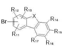
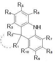
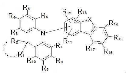
상기 목적을 달성하기 위해 본 발명은 하기 화학식 1로 표시되는 아크리딘 유도체를 포함하는 유기발광 화합물을 제공한다:In order to achieve the above object, the present invention provides an organic light-emitting compound comprising an acridine derivative represented by the following Formula 1:
[화학식 1][Formula 1]

상기 식에서,In the above formula,
X는 치환 또는 비치환된 C, O, P, S, Se 또는 Si이고, X가 O일 경우 아크리딘의 질소 원자는 헤테로아릴계 모이어티의 3번 위치에는 결합될 수 없고;X is a substituted or unsubstituted C, O, P, S, Se or Si, and when X is O, the nitrogen atom of acridine cannot be bonded to the 3rd position of the heteroaryl-based moiety;
R1 내지 R17은 각각 독립적으로, 수소; 중수소; 중수소, 할로겐, 아미노기, 니트릴기, 니트로기로 치환되거나 치환되지 않은 C1-30의 알킬기; 중수소, 할로겐, 아미노기, 니트릴기, 니트로기로 치환되거나 치환되지 않은 C2-30의 알케닐기; 중수소, 할로겐, 아미노기, 니트릴기, 니트로기로 치환되거나 치환되지 않은 C2-30의 알키닐기; 중수소, 할로겐, 아미노기, 니트릴기, 니트로기로 치환되거나 치환되지 않은 C1-30의 알콕시기; 중수소, 할로겐, 아미노기, 니트릴기, 니트로기로 치환되거나 치환되지 않은 C6-30의 아릴옥시기; 중수소, 할로겐, 아미노기, 니트릴기, 니트로기로 치환되거나 치환되지 않은 C6-36의 아릴기; 또는 중수소, 할로겐, 아미노기, 니트릴기, 니트로기로 치환되거나 치환되지 않은 C2-36의 헤테로아릴기이고, 선택적으로, 상기 R1 내지 R17 중 인접한 기가 서로 결합하여 포화 또는 불포화 탄소 고리를 형성할 수 있다.
R 1 to R 17 are each independently hydrogen; heavy hydrogen; C 1-30 alkyl group substituted or unsubstituted with deuterium, halogen, amino group, nitrile group, nitro group; C 2-30 alkenyl group substituted or unsubstituted with deuterium, halogen, amino group, nitrile group, nitro group; C 2-30 alkynyl group substituted or unsubstituted with deuterium, halogen, amino group, nitrile group, nitro group; C 1-30 alkoxy group substituted or unsubstituted with deuterium, halogen, amino group, nitrile group, nitro group; C 6-30 aryloxy group substituted or unsubstituted with deuterium, halogen, amino group, nitrile group, nitro group; C 6-36 aryl group substituted or unsubstituted with deuterium, halogen, amino group, nitrile group, nitro group; Or C 2-36 heteroaryl group substituted or unsubstituted with deuterium, halogen, amino group, nitrile group, nitro group, and optionally, adjacent groups of R 1 to R 17 are bonded to each other to form a saturated or unsaturated carbon ring. I can.
또한 하기 화학식 1-1과 화학식 1-2를 반응시키는 단계를 포함하는 특징으로 하는 화학식 1의 제조방법을 제공한다:In addition, it provides a method for preparing Formula 1 comprising the step of reacting Formula 1-1 with Formula 1-2:
[화학식 1-1][Formula 1-1]

[화학식 1-2][Formula 1-2]
상기에서 X 및 R1 내지 R17은 화학식 1에서 정의한 바와 같다.
In the above, X and R 1 to R 17 are as defined in Formula 1.
또한, 본 발명은 상기 화학식 1로 표시되는 화합물을 발광물질로서 유기물층에 포함하는 유기발광소자를 제공한다.
In addition, the present invention provides an organic light-emitting device including the compound represented by Formula 1 as a light-emitting material in an organic material layer.
본 발명의 유기발광 화합물은 아크리딘 유도체와 고리화합물의 적절한 조화를 통해 유기물층 내에서의 전하균형을 조절함으로써, 휘도, 전력효율, 내열성, 전하수송 성능 및 전하주입 성능이 우수하여 색순도 및 발광효율을 증가시킬 수 있으므로, 유기발광소자의 기능층 재료 및 발광층의 호스트나 도판트 중 하나 이상에 적용할 수 있다. 따라서, 본 발명의 화합물을 포함하는 유기발광소자는 낮은 구동전압과 높은 발광휘도 및 발광효율을 나타내며, 이에 따라 풀 칼라 유기 패널에서 성능 극대화 및 수명 향상을 제공할 수 있다.
The organic light-emitting compound of the present invention is excellent in brightness, power efficiency, heat resistance, charge transport performance and charge injection performance by controlling the charge balance in the organic material layer through appropriate harmony of the acridine derivative and the cyclic compound. Since can be increased, it can be applied to one or more of the functional layer material of the organic light emitting device and the host or dopant of the light emitting layer. Accordingly, the organic light-emitting device including the compound of the present invention exhibits a low driving voltage, high luminance and luminous efficiency, thereby maximizing performance and improving lifespan in a full-color organic panel.
도 1은 본 발명의 일 실시예에 따른 OLED의 단면을 개략적으로 도시한 것이며,
도 2는 유기발광현상에 의한 발광원리를 갖는 유기전계발광 다이오드의 밴드 다이어그램을 나타낸 것이다.
도면의 부호
10 : 기판
11 : 양극
12 : 정공주입층
13 : 정공전달층
14 : 발광층
15 : 전자전달층
16: 음극1 schematically shows a cross-section of an OLED according to an embodiment of the present invention,
2 shows a band diagram of an organic light emitting diode having a light emitting principle by an organic light emitting phenomenon.
The symbol of the drawing
10: substrate
11: anode
12: hole injection layer
13: hole transport layer
14: light emitting layer
15: electron transport layer
16: cathode
하기 화학식 1로 표시되는 본 발명의 화합물은 아크리딘계 모이어티(moiety)와 아릴계 또는 헤테로아릴계 모이어티가 아크리딘의 질소 원자에 직접 연결되는 것을 특징으로 한다:The compound of the present invention represented by the following Formula 1 is characterized in that an acridine-based moiety and an aryl-based or heteroaryl-based moiety are directly connected to the nitrogen atom of acridine:
<화학식 1><Formula 1>

상기 식에서,In the above formula,
X는 치환 또는 비치환된 C, O, P, S, Se 또는 Si이고, X가 O일 경우 아크리딘의 질소 원자는 헤테로아릴계 모이어티의 3번 위치에는 결합될 수 없고;X is a substituted or unsubstituted C, O, P, S, Se or Si, and when X is O, the nitrogen atom of acridine cannot be bonded to the 3rd position of the heteroaryl-based moiety;
R1 내지 R17은 각각 독립적으로, 수소; 중수소; 중수소, 할로겐, 아미노기, 니트릴기, 니트로기로 치환되거나 치환되지 않은 C1-30의 알킬기; 중수소, 할로겐, 아미노기, 니트릴기, 니트로기로 치환되거나 치환되지 않은 C2-30의 알케닐기; 중수소, 할로겐, 아미노기, 니트릴기, 니트로기로 치환되거나 치환되지 않은 C2-30의 알키닐기; 중수소, 할로겐, 아미노기, 니트릴기, 니트로기로 치환되거나 치환되지 않은 C1-30의 알콕시기; 중수소, 할로겐, 아미노기, 니트릴기, 니트로기로 치환되거나 치환되지 않은 C6-30의 아릴옥시기; 중수소, 할로겐, 아미노기, 니트릴기, 니트로기로 치환되거나 치환되지 않은 C6-36의 아릴기; 또는 중수소, 할로겐, 아미노기, 니트릴기, 니트로기로 치환되거나 치환되지 않은 C2-36의 헤테로아릴기이고, 선택적으로, 상기 R1 내지 R17 중 인접한 기가 서로 결합하여 포화 또는 불포화 탄소 고리를 형성할 수 있다. R 1 to R 17 are each independently hydrogen; heavy hydrogen; C 1-30 alkyl group substituted or unsubstituted with deuterium, halogen, amino group, nitrile group, nitro group; C 2-30 alkenyl group substituted or unsubstituted with deuterium, halogen, amino group, nitrile group, nitro group; C 2-30 alkynyl group substituted or unsubstituted with deuterium, halogen, amino group, nitrile group, nitro group; C 1-30 alkoxy group substituted or unsubstituted with deuterium, halogen, amino group, nitrile group, nitro group; C 6-30 aryloxy group substituted or unsubstituted with deuterium, halogen, amino group, nitrile group, nitro group; C 6-36 aryl group substituted or unsubstituted with deuterium, halogen, amino group, nitrile group, nitro group; Or C 2-36 heteroaryl group substituted or unsubstituted with deuterium, halogen, amino group, nitrile group, nitro group, and optionally, adjacent groups of R 1 to R 17 are bonded to each other to form a saturated or unsaturated carbon ring. I can.
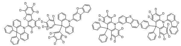
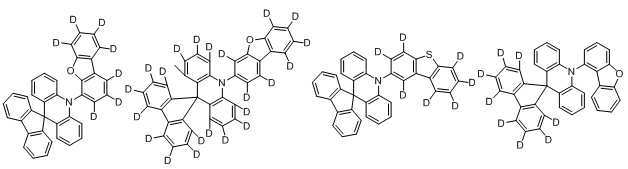
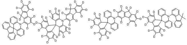
상기 R1 내지 R10는 각각 중수소로 치환되는 경우에는, R1 내지 R10 중 적어도 20%, 바람직하게는 적어도 40%, 더욱 바람직하게는 적어도 50%로 중수소화 될 수 있다.When each of R 1 to R 10 is substituted with deuterium, it may be deuterated to at least 20%, preferably at least 40%, more preferably at least 50% of R 1 to R 10 .
또한, 상기 화합물에서 아크리딘계 모이어티(moiety)의 질소 원자에 직접 연결된 아릴계 또는 헤테로아릴계 모이어티가 중수소로 치환되는 경우에는, 적어도 50% 중수소화 되는 것이 바람직하다.In addition, when the aryl-based or heteroaryl-based moiety directly connected to the nitrogen atom of the acridine-based moiety in the compound is substituted with deuterium, it is preferably deuterated by at least 50%.
또한, 상기 X 및 R1 내지 R17의 치환기는 각각 독립적으로 중수소, 할로겐, 니트릴기, 니트로기, C1-30의 알킬기, C1-30의 알콕시기, C3-30의 시클로알킬기, C3-30의 헤테로시클로알킬기, C6-30의 아릴기, C5-30의 헤테로아릴기, C1-30의 알킬옥시기, C6-30의 아릴옥시기 및 C6-30의 아릴아민기로 이루어진 군에서 선택되는 하나 이상의 치환기로 치환되는 것이 바람직하나, 이에 한정되지는 않으며, 인접한 기가 서로 결합하여 포화 또는 불포화 탄소 고리를 형성할 수 있다.In addition, the substituents of X and R 1 to R 17 are each independently deuterium, halogen, nitrile group, nitro group, C 1-30 alkyl group, C 1-30 alkoxy group, C 3-30 cycloalkyl group, C 3-30 heterocycloalkyl group, C 6-30 aryl group, C 5-30 heteroaryl group, C 1-30 alkyloxy group, C 6-30 aryloxy group and C 6-30 arylamine It is preferable to be substituted with one or more substituents selected from the group consisting of groups, but is not limited thereto, and adjacent groups may be bonded to each other to form a saturated or unsaturated carbon ring.
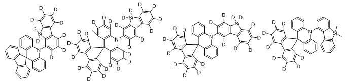
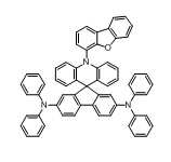
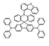
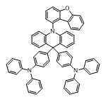
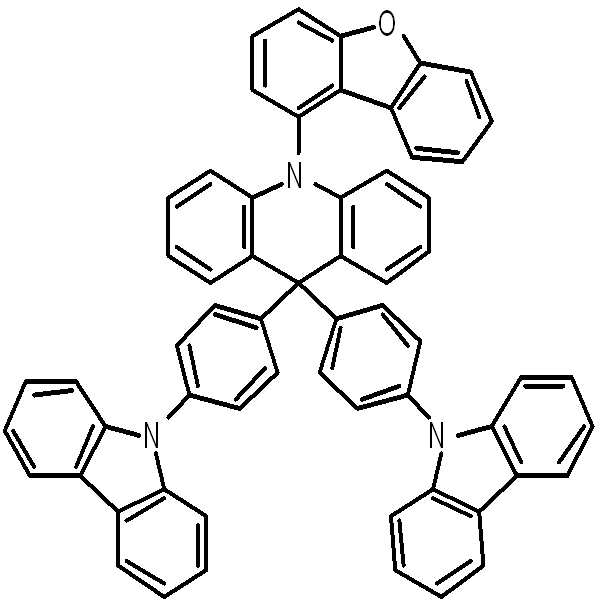
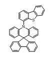
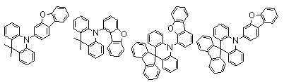
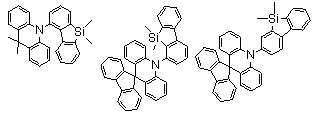
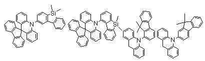
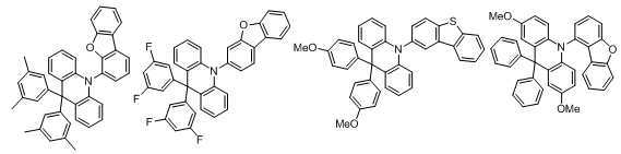
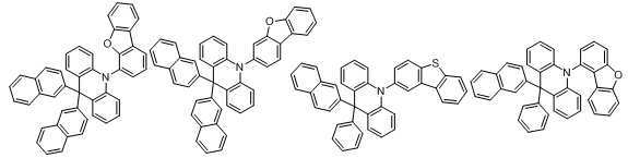
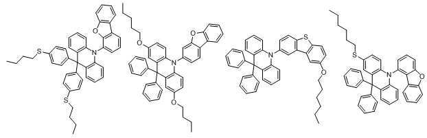
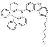
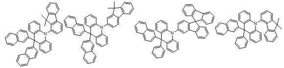
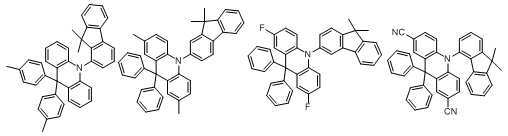
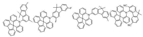
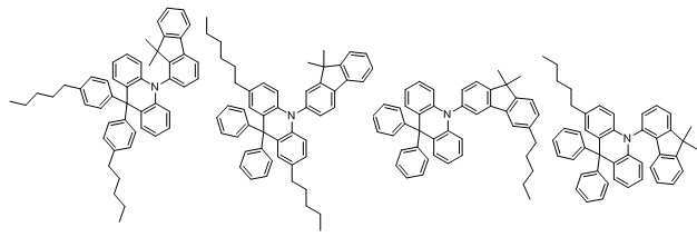
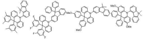
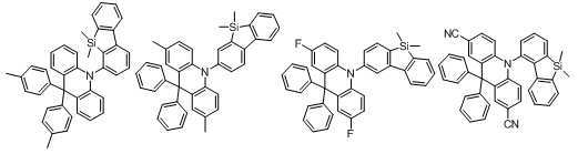
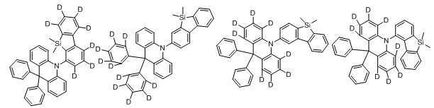
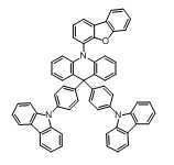
본 발명에 있어서, 상기 화학식 1로 표시되는 화합물의 바람직한 예는 다음과 같다:In the present invention, preferred examples of the compound represented by Formula 1 are as follows:


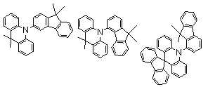
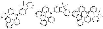


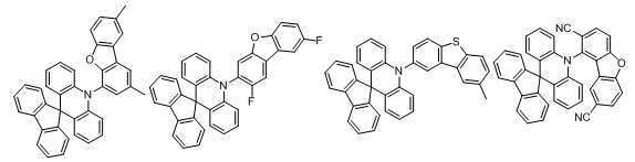


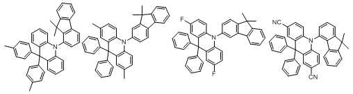


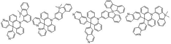

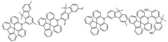


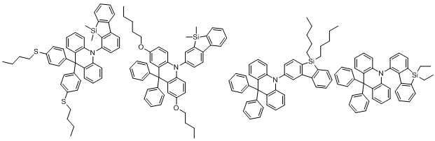


본 발명에 따른 화학식 1의 화합물은 아크리딘계 모이어티와 아릴계 또는 헤테로아릴계 모이어티가 아크리딘의 질소 원자에 직접 연결되어 아크리딘 유도체와 고리화합물의 적절한 조화를 통해 유기물층 내에서의 전하균형을 조절한다. 이로 인해 휘도, 전력효율, 내열성, 전하수송 성능 및 전하주입 성능이 우수하여 색순도 및 발광효율을 증가시킬 수 있으므로, 유기발광소자의 기능층 재료 및 발광층의 호스트나 도판트 중 하나 이상에 적용할 수 있다. In the compound of Formula 1 according to the present invention, an acridine-based moiety and an aryl-based or heteroaryl-based moiety are directly connected to the nitrogen atom of acridine, so that the acridine derivative and the cyclic compound are properly combined in the organic material layer. Controls charge balance. Due to this, it is possible to increase color purity and luminous efficiency due to excellent luminance, power efficiency, heat resistance, charge transport performance and charge injection performance, so it can be applied to one or more of the functional layer material of the organic light emitting device and the host or dopant of the light emitting layer. have.
따라서, 본 발명의 화합물을 유기발광소자에 적용하면, 발광소자의 구동전압 및 발광 효율 등의 특성을 향상 시킬 수 있다.
Therefore, when the compound of the present invention is applied to an organic light emitting device, characteristics such as driving voltage and light emission efficiency of the light emitting device can be improved.
또한 본 발명은 하기 화학식 1-1과 화학식 1-2를 반응시키는 단계를 포함하는 특징으로 하는 화학식 1의 제조방법을 제공한다:In addition, the present invention provides a method for preparing Formula 1 comprising the step of reacting Formula 1-1 and Formula 1-2 below:
[화학식 1-1][Formula 1-1]
[화학식 1-2][Formula 1-2]

상기에서 X 및 R1 내지 R17은 화학식 1에서 정의한 바와 같다.In the above, X and R 1 to R 17 are as defined in Formula 1.
구체적인 일예로 본 발명에 따른 화학식 1의 화합물은 하기 반응식 1에 따른 방법에 따라 제조될 수 있다.As a specific example, the compound of Formula 1 according to the present invention may be prepared according to the method according to Scheme 1 below.
[반응식 1][Scheme 1]

상기 반응식 1에서 X는 화학식 1에서 정의한 바와 같으며, 각각의 R은 각각 화학식 1-1의 R1 및 R2에 대응된다.In Reaction Scheme 1, X is as defined in Formula 1, and each R corresponds to R 1 and R 2 in Formula 1-1, respectively.
또한, 본 발명은 발광물질로서 상기 화학식 1로 표시되는 화합물을 유기물층에 포함하는 유기발광소자를 제공한다. 이때, 본 발명의 화합물은 단독으로 사용되거나 공지의 유기발광 화합물과 함께 사용될 수 있다.In addition, the present invention provides an organic light emitting device including the compound represented by Formula 1 as a light emitting material in an organic material layer. At this time, the compound of the present invention may be used alone or together with a known organic light emitting compound.
또한 본 발명의 유기발광소자는 상기 화학식 1로 표시되는 화합물을 포함하는 1층 이상의 유기물층을 포함하는 바, 상기 유기발광소자의 제조방법을 설명하면 다음과 같다.In addition, the organic light-emitting device of the present invention includes one or more organic material layers including the compound represented by Chemical Formula 1, and a method of manufacturing the organic light-emitting device will be described below.
상기 유기발광소자는 애노드(anode)와 캐소드(cathod) 사이에 정공주입층(HIL), 정공수송층(HTL), 발광층(EML), 전자수송층(ETL), 전자주입층(EIL) 등의 유기물층을 1 개 이상 포함할 수 있다.The organic light emitting device includes an organic material layer such as a hole injection layer (HIL), a hole transport layer (HTL), a light emitting layer (EML), an electron transport layer (ETL), and an electron injection layer (EIL) between an anode and a cathode. It can contain more than one.
먼저, 기판 상부에 높은 일함수를 갖는 애노드 전극용 물질을 증착시켜 애노드를 형성한다. 이때, 상기 기판은 통상의 유기발광소자에서 사용되는 기판을 사용할 수 있으며, 특히 기계적 강도, 열적 안정성, 투명성, 표면평활성, 취급용이성, 및 방수성이 우수한 유리 기판 또는 투명 플라스틱 기판을 사용하는 것이 좋다. 또한, 애노드 전극용 물질로는 투명하고 전도성이 우수한 산화인듐주석(ITO), 산화인듐아연(IZO), 산화주석(SnO2), 산화아연(ZnO) 등을 사용할 수 있다. 상기 애노드 전극용 물질은 통상의 애노드 형성방법에 의해 증착할 수 있으며, 구체적으로 증착법 또는 스퍼터링법에 의해 증착할 수 있다.First, an anode is formed by depositing a material for an anode electrode having a high work function on the substrate. At this time, the substrate may be a substrate used in a conventional organic light emitting device, in particular, it is preferable to use a glass substrate or a transparent plastic substrate excellent in mechanical strength, thermal stability, transparency, surface smoothness, ease of handling, and water resistance. In addition, as a material for the anode electrode, indium tin oxide (ITO), indium zinc oxide (IZO), tin oxide (SnO 2 ), zinc oxide (ZnO), and the like, which are transparent and have excellent conductivity, may be used. The material for the anode electrode may be deposited by a conventional anode forming method, and specifically, may be deposited by a vapor deposition method or a sputtering method.
그 다음, 상기 애노드 전극 상부에 정공주입층 물질을 진공증착법, 스핀코팅법, 캐스트법, LB(Langmuir-Blodgett)법 등과 같은 방법에 의해 형성할 수 있지만, 균일한 막질을 얻기 쉽고, 또한 핀정공이 발생하기 어렵다는 등의 점에서 진공증착법에 의해 형성하는 것이 바람직하다. 상기 진공증착법에 의해 정공주입층을 형성하는 경우 그 증착조건은 정공주입층의 재료로서 사용하는 화합물, 목적하는 정공주입층의 구조 및 열적특성 등에 따라 다르지만, 일반적으로 50-500 ℃의 증착온도, 10-8 내지 10-3 torr의 진공도, 0.01 내지 100 Å/sec의 증착속도, 10 Å 내지 5 ㎛의 층 두께 범위에서 적절히 선택하는 것이 바람직하다.Then, the material of the hole injection layer on the anode electrode can be formed by a method such as a vacuum deposition method, a spin coating method, a cast method, or a LB (Langmuir-Blodgett) method, but it is easy to obtain a uniform film quality, and It is preferable to form by a vacuum evaporation method from the viewpoint of being difficult to generate. When the hole injection layer is formed by the vacuum deposition method, the deposition conditions vary depending on the compound used as the material of the hole injection layer, the structure and thermal characteristics of the target hole injection layer, etc., but in general, a deposition temperature of 50-500 ℃, It is preferable to appropriately select a vacuum degree of 10 -8 to 10 -3 torr, a deposition rate of 0.01 to 100 Å/sec, and a layer thickness of 10 Å to 5 µm.
상기 정공주입층 물질은 특별히 제한되지 않으며, 미국특허 제4,356,429호에 개시된 구리 프탈로시아닌 등의 프탈로시아닌 화합물 또는 스타버스트형 아민 유도체류인 TCTA(4,4',4"-트리(N-카바졸릴)트리페닐아민), m-MTDATA(4,4',4"-트리스(3-메틸페닐아미노)트리페닐아민), m-MTDAPB(4,4',4"-트리스(3-메틸페닐아미노)페녹시벤젠), HI-406(N1,N1'-(비페닐-4,4'-디일)비스(N1-(나프탈렌-1-일)-N4,N4-디페닐벤젠-1,4-디아민) 등을 정공주입층 물질로 사용할 수 있다.The hole injection layer material is not particularly limited, and TCTA(4,4',4"-tri(N-carbazolyl) tree, which is a phthalocyanine compound such as copper phthalocyanine disclosed in U.S. Patent No. 4,356,429 or a starburst-type amine derivative Phenylamine), m-MTDATA(4,4',4"-tris(3-methylphenylamino)triphenylamine), m-MTDAPB(4,4',4"-tris(3-methylphenylamino)phenoxybenzene ), HI-406(N 1 ,N 1 '-(biphenyl-4,4'-diyl) bis(N 1 -(naphthalen- 1 -yl)-N 4 ,N 4 -diphenylbenzene-1,4 -Diamine) or the like can be used as a material for the hole injection layer.
다음으로 상기 정공주입층 상부에 정공수송층 물질을 진공증착법, 스핀코팅법, 캐스트법, LB법 등과 같은 방법에 의해 형성할 수 있지만, 균일한 막질을 얻기 쉽고, 핀정공이 발생하기 어렵다는 점에서 진공증착법에 의해 형성하는 것이 바람직하다. 상기 진공증착법에 의해 정공수송층을 형성하는 경우 그 증착조건은 사용하는 화합물에 따라 다르지만 일반적으로 정공주입층의 형성과 거의 동일한 조건 범위에서 선택하는 것이 좋다.Next, the material of the hole transport layer on the hole injection layer can be formed by a method such as vacuum deposition, spin coating, casting, LB method, etc., but it is easy to obtain a uniform film quality and is difficult to generate pin holes. It is preferably formed by a vapor deposition method. When the hole transport layer is formed by the vacuum deposition method, the deposition conditions vary depending on the compound to be used, but in general, it is preferable to select within the same range of conditions as the hole injection layer formation.
또한, 상기 정공수송층 물질은 특별히 제한되지는 않으며, 정공수송층에 사용되고 있는 통상의 공지 물질 중에서 임의로 선택하여 사용할 수 있다. 구체적으로, 상기 정공수송층 물질은 N-페닐카바졸, 폴리비닐카바졸 등의 카바졸 유도체, N,N'-비스(3-메틸페닐)-N,N'-디페닐-[1,1-비페닐]-4,4'-디아민(TPD), N.N'-디(나프탈렌-1-일)-N,N'-디페닐 벤지딘(α-NPD) 등의 방향족 축합환을 가지는 통상의 아민 유도체 등이 사용될 수 있다.In addition, the material for the hole transport layer is not particularly limited, and may be arbitrarily selected from conventional known materials used for the hole transport layer. Specifically, the material for the hole transport layer is a carbazole derivative such as N-phenylcarbazole and polyvinylcarbazole, N,N'-bis(3-methylphenyl)-N,N'-diphenyl-[1,1-ratio Phenyl]-4,4'-diamine (TPD), N.N'-di(naphthalen-1-yl)-N,N'-diphenyl benzidine (α-NPD), etc. Derivatives and the like can be used.
그 후, 상기 정공수송층 상부에 발광층 물질을 진공증착법, 스핀코팅법, 캐스트법, LB법 등과 같은 방법에 의해 형성할 수 있지만, 균일한 막질을 얻기 쉽고, 핀정공이 발생하기 어렵다는 점에서 진공증착법에 의해 형성하는 것이 바람직하다. 상기 진공증착법에 의해 발광층을 형성하는 경우 그 증착조건은 사용하는 화합물에 따라 다르지만 일반적으로 정공주입층의 형성과 거의 동일한 조건 범위에서 선택하는 것이 좋다. 또한, 상기 발광층 재료는 본 발명의 화학식 1로 표시되는 화합물을 호스트 또는 도펀트로 사용할 수 있다.Thereafter, the light emitting layer material can be formed on the hole transport layer by a method such as vacuum deposition, spin coating, casting, LB method, etc., but it is easy to obtain a uniform film quality and is difficult to generate pin holes. It is preferable to form by. When the light emitting layer is formed by the vacuum deposition method, the deposition conditions vary depending on the compound to be used, but in general, it is preferable to select it within the same range of conditions as the hole injection layer formation. In addition, the light-emitting layer material may use the compound represented by Formula 1 of the present invention as a host or dopant.
상기 화학식 1로 표시되는 화합물을 발광 호스트로 사용하는 경우, 인광 또는 형광 도펀트를 함께 사용하여 발광층을 형성할 수 있다. 이때, 형광 도펀트로는 이데미츠사(Idemitsu사)에서 구입 가능한 IDE102 또는 IDE105, 또는 BD142(N6,N12-비스(3,4-디메틸페닐)-N6,N12-디메시틸크리센-6,12-디아민)를 사용할 수 있으며, 인광 도펀트로는 녹색 인광 도펀트 Ir(ppy)3(트리스(2-페닐피리딘) 이리듐), 청색 인광 도펀트인 F2Irpic(이리듐(Ⅲ) 비스[4,6-다이플루오로페닐)-피리디나토-N,C2'] 피콜린산염), UDC사의 적색 인광 도펀트 RD61 등이 공동 진공증착(도핑)될 수 있다. 도펀트의 도핑농도는 특별히 제한되지 않으나, 호스트 100 중량부 대비 도펀트가 0.01 내지 15 중량부로 도핑되는 것이 바람직하다. 만약 도펀트의 함량이 0.01 중량부 미만일 경우에는 도펀트량이 충분치 못하여 발색이 제대로 이루어지지 않는다는 문제점이 있으며, 15 중량부를 초과할 경우에는 농도 소광 현상으로 인해 효율이 급격히 감소된다는 문제점이 있다.When the compound represented by Formula 1 is used as a light emitting host, a phosphorescent or fluorescent dopant may be used together to form a light emitting layer. At this time, as the fluorescent dopant, IDE102 or IDE105 available from Idemitsu, or BD142 (N 6 ,N 12 -bis(3,4-dimethylphenyl)-N 6 ,N 12 -dimethylcrysen- 6,12-diamine) can be used, and as the phosphorescent dopant, the green phosphorescent dopant Ir(ppy) 3 (tris(2-phenylpyridine) iridium), the blue phosphorescent dopant F2Irpic (iridium(III) bis[4,6- Difluorophenyl)-pyridinato-N,C2'] picolinate), UDC's red phosphorescent dopant RD61, etc. may be co-vacuum deposited (doped). The doping concentration of the dopant is not particularly limited, but it is preferable that the dopant is doped at 0.01 to 15 parts by weight relative to 100 parts by weight of the host. If the content of the dopant is less than 0.01 parts by weight, there is a problem in that the dopant amount is insufficient and color development is not performed properly. If the content of the dopant is more than 15 parts by weight, there is a problem that the efficiency is rapidly reduced due to concentration quenching.
또한, 발광층에 인광 도펀트와 함께 사용할 경우에는 삼중항 여기자 또는 정공이 전자수송층으로 확산되는 현상을 방지하기 위하여 정공억제재료(HBL)를 추가로 진공증착법 또는 스핀코팅법에 의해 적층시키는 것이 바람직하다. 이때 사용할 수 있는 정공억제물질은 특별히 제한되지는 않으나, 정공억제재료로 사용되고 있는 공지의 것에서 임의의 것을 선택해서 이용할 수 있다. 예를 들면, 옥사디아졸 유도체나 트리아졸 유도체, 페난트롤린 유도체, 또는 일본특개평 11-329734(A1)에 기재되어 있는 정공억제재료 등을 들 수 있으며, 대표적으로 Balq(비스(8-하이드록시-2-메틸퀴놀리놀나토)-알루미늄 비페녹사이드), 페난트롤린(phenanthrolines)계 화합물(예: UDC사 BCP(바쏘쿠프로인)) 등을 사용할 수 있다.In addition, in the case of using with a phosphorescent dopant in the light emitting layer, it is preferable to additionally laminate a hole inhibiting material (HBL) by vacuum deposition or spin coating in order to prevent diffusion of triplet excitons or holes into the electron transport layer. The hole-suppressing material that can be used at this time is not particularly limited, but any of the known materials used as hole-suppressing materials may be selected and used. For example, oxadiazole derivatives, triazole derivatives, phenanthroline derivatives, or hole inhibiting materials described in Japanese Unexamined Patent Application Publication No. Hei 11-329734(A1), and the like, and representatively Balq (bis(8-hydride) Roxy-2-methylquinolinolnato)-aluminum biphenoxide), phenanthrolines-based compounds (eg, UDC's BCP (basocuproin)) and the like can be used.
상기와 같이 형성된 발광층 상부에는 전자수송층이 형성되는데, 이때 상기 전자수송층은 진공증착법, 스핀코팅법, 캐스트법 등의 방법으로 형성되며, 특히 진공증착법에 의해 형성하는 것이 바람직하다.An electron transport layer is formed on the light emitting layer formed as described above, wherein the electron transport layer is formed by a method such as a vacuum deposition method, a spin coating method, or a cast method, and is particularly preferably formed by a vacuum deposition method.
상기 전자수송층 재료는 전자주입전극으로부터 주입된 전자를 안정하게 수송하는 기능을 하는 것으로서 그 종류가 특별히 제한되지는 않으며, 예를 들어 퀴놀린 유도체, 특히 트리스(8-퀴놀리놀라토)알루미늄(Alq3), 또는 ET4(6,6'-(3,4-디메시틸-1,1-디메틸-1H-실올-2,5-디일)디-2,2'-비피리딘)을 사용할 수 있다. 또한, 전자수송층 상부에 캐소드로부터 전자의 주입을 용이하게 하는 기능을 가지는 물질인 전자주입층(EIL)이 적층될 수 있으며, 전자주입층 물질로는 LiF, NaCl, CsF, Li2O, BaO 등의 물질을 이용할 수 있다.The electron transport layer material has a function of stably transporting electrons injected from the electron injection electrode, and its kind is not particularly limited, and, for example, a quinoline derivative, especially tris(8-quinolinolato)aluminum (Alq 3 ), or ET4 (6,6'-(3,4-dimethyl-1,1-dimethyl-1H-silol-2,5-diyl)di-2,2'-bipyridine) can be used. In addition, an electron injection layer (EIL), which is a material that facilitates injection of electrons from the cathode, may be stacked on the electron transport layer, and the electron injection layer materials include LiF, NaCl, CsF, Li 2 O, BaO, etc. The material of can be used.
또한, 상기 전자수송층의 증착조건은 사용하는 화합물에 따라 다르지만, 일반적으로 정공주입층의 형성과 거의 동일한 조건 범위에서 선택하는 것이 좋다.In addition, the deposition conditions of the electron transport layer vary depending on the compound to be used, but it is generally preferable to select the electron transport layer within the same range of conditions as the formation of the hole injection layer.
그 뒤, 상기 전자수송층 상부에 전자주입층 물질을 형성할 수 있으며, 이때 상기 전자수송층은 통상의 전자주입층 물질을 진공증착법, 스핀코팅법, 캐스트법 등의 방법으로 형성되며, 특히 진공증착법에 의해 형성하는 것이 바람직하다.Thereafter, an electron injection layer material may be formed on the electron transport layer, wherein the electron transport layer is formed by a vacuum deposition method, a spin coating method, a cast method, etc., and in particular, a vacuum deposition method. It is preferably formed by.
마지막으로 전자주입층 상부에 캐소드 형성용 금속을 진공증착법이나 스퍼터링법 등의 방법에 의해 형성하고 캐소드로 사용한다. 여기서 캐소드 형성용 금속으로는 낮은 일함수를 가지는 금속, 합금, 전기전도성 화합물, 및 이들의 혼합물을 사용할 수 있다. 구체적인 예로는 리튬(Li), 마그네슘(Mg), 알루미늄(Al), 알루미늄-리튬(Al-Li), 칼슘(Ca), 마그네슘-인듐(Mg-In), 마그네슘-은(Mg-Ag) 등이 있다. 또한, 전면 발광소자를 얻기 위하여 ITO, IZO를 사용한 투과형 캐소드를 사용할 수도 있다.Finally, a metal for forming a cathode is formed on the electron injection layer by a method such as vacuum deposition or sputtering, and is used as a cathode. Here, as the metal for forming the cathode, a metal having a low work function, an alloy, an electroconductive compound, and a mixture thereof may be used. Specific examples include lithium (Li), magnesium (Mg), aluminum (Al), aluminum-lithium (Al-Li), calcium (Ca), magnesium-indium (Mg-In), magnesium-silver (Mg-Ag), etc. There is this. In addition, a transmissive cathode using ITO or IZO may be used to obtain a top light emitting device.
본 발명의 유기발광소자는 애노드, 정공주입층, 정공수송층, 발광층, 전자수송층, 전자주입층, 캐소드 구조의 유기발광소자 뿐만 아니라, 다양한 구조의 유기발광소자의 구조가 가능하며, 필요에 따라 1층 또는 2층의 중간층을 더 형성하는 것도 가능하다.The organic light-emitting device of the present invention can have an anode, a hole injection layer, a hole transport layer, a light-emitting layer, an electron transport layer, an electron injection layer, an organic light-emitting device having a cathode structure, as well as an organic light-emitting device having a variety of structures. It is also possible to further form a layer or an intermediate layer of two layers.
상기와 같이 본 발명에 따라 형성되는 각 유기물층의 두께는 요구되는 정도에 따라 조절할 수 있으며, 바람직하게는 10 내지 1,000 ㎚이며, 더욱 바람직하게는 20 내지 150 ㎚인 것이 좋다.As described above, the thickness of each organic material layer formed according to the present invention can be adjusted according to the required degree, preferably 10 to 1,000 nm, more preferably 20 to 150 nm.
또한 본 발명은 상기 화학식 1로 표시되는 화합물을 포함하는 유기물층은 유기물층의 두께를 분자 단위로 조절할 수 있기 때문에 표면이 균일하며, 형태안정성이 뛰어난 장점이 있다.In addition, in the present invention, the organic material layer including the compound represented by Chemical Formula 1 has an advantage of having a uniform surface and excellent shape stability because the thickness of the organic material layer can be controlled on a molecular basis.
본 발명의 유기발광 화합물은 휘도, 전력효율, 내열성, 전하수송 성능 및 전하주입 성능이 우수하여 색순도 및 발광효율을 증가시킬 수 있으므로, 유기발광소자의 발광물질로 사용되어 유기발광소자에 낮은 구동전압과 높은 발광휘도 및 발광효율을 나타내며, 이에 따라 풀 칼라 유기 패널에서 성능 극대화 및 수명 향상을 제공할 수 있다.
The organic light-emitting compound of the present invention has excellent luminance, power efficiency, heat resistance, charge transport performance and charge injection performance to increase color purity and luminous efficiency, so it is used as a light-emitting material of an organic light-emitting device and has a low driving voltage for the organic light-emitting device. And high luminous luminance and luminous efficiency, thereby maximizing performance and improving lifespan in a full-color organic panel.
이하, 본 발명의 이해를 돕기 위하여 바람직한 실시예를 제시하나, 하기 실시예는 본 발명을 예시하는 것일 뿐 본 발명의 범위가 하기 실시예에 한정되는 것은 아니다.
Hereinafter, preferred examples are presented to aid in the understanding of the present invention, but the following examples are only illustrative of the present invention, and the scope of the present invention is not limited to the following examples.
[실시예 1: 화합물 1의 합성][Example 1: Synthesis of Compound 1]
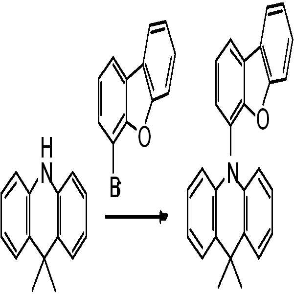
9,9-dimethyl-9,10-dihydroacridine 5 g, 4-bromodibenzo[b,d]furan 7.1 g, t-BuONa 3.5 g, Pd2(dba)3 0.9 g, (t-Bu)3P 1.2 ml를 톨루엔 100 ml에 녹인 후 환류 교반하였다. 반응이 종결되면 증류수와 EA로 추출한 후 컬럼정제하여 화합물 1을 얻었다. (수율 61%)9,9-dimethyl-9,10-dihydroacridine 5 g, 4-bromodibenzo[b,d]furan 7.1 g, t-BuONa 3.5 g, Pd 2 (dba) 3 0.9 g, (t-Bu) 3 P 1.2 ml Was dissolved in 100 ml of toluene and stirred under reflux. When the reaction was completed, the mixture was extracted with distilled water and EA, followed by column purification to obtain compound 1. (61% yield)
m/z: 375.16 (100.0%), 376.17 (29.5%), 377.17 (4.4%)m/z: 375.16 (100.0%), 376.17 (29.5%), 377.17 (4.4%)
[실시예 2: 화합물 2의 합성][Example 2: Synthesis of Compound 2]

2-bromo-N-phenylaniline 10 g을 THF 100 ml에 녹인 후 반응 온도를 -78 ℃로 낮추고 BuLi 2.5 M을 20 ml 천천히 적가하고 1시간 동안 교반하였다. Benzophenone 11 g을 THF 100 ml에 녹인 후 천천히 적가한 후 실온으로 온도를 높이고 12시간 교반하였다. 반응이 종결된 후 증류수와 MC로 추출하고 무수황산마그네슘으로 물을 제거한 후 감압여과하여 얻은 고체를 더 이상의 정제 없이 Acetic acid 100 ml에 녹인 후 황산 7 ml를 적가하고 환류교반하였다. 반응이 종결된 후 증류수와 MC로 추출하고 생성된 고체를 컬럼 정제하여 I2 7.1 g을 얻었다. (수율 53%)After dissolving 10 g of 2-bromo-N-phenylaniline in 100 ml of THF, the reaction temperature was lowered to -78 °C, and 20 ml of BuLi 2.5 M was slowly added dropwise and stirred for 1 hour. After 11 g of benzophenone was dissolved in 100 ml of THF, slowly added dropwise, the temperature was raised to room temperature, and the mixture was stirred for 12 hours. After the reaction was completed, the mixture was extracted with distilled water and MC, water was removed with anhydrous magnesium sulfate, and the solid obtained by filtration under reduced pressure was dissolved in 100 ml of Acetic acid without further purification, and then 7 ml of sulfuric acid was added dropwise and stirred under reflux. After the reaction was completed, extraction was performed with distilled water and MC, and the resulting solid was purified by column to obtain 7.1 g of I 2 . (Yield 53%)
상기 단계의 I2 7g, 4-bromodibenzo[b,d]furan 6.5 g, t-BuONa 3 g, Pd2(dba)3 0.7 g, (t-Bu)3P 1 ml를 톨루엔 150 ml에 녹인 후 환류 교반하였다. 반응이 종결되면 증류수와 EA로 추출한 후 컬럼정제하여 화합물을 얻었다. (수율 67%)After dissolving 7 g of I 2 , 6.5 g of 4-bromodibenzo[b,d]furan, 3 g of t-BuONa, 0.7 g of Pd 2 (dba) 3 , 1 ml of (t-Bu) 3 P in 150 ml of toluene, Stir at reflux. When the reaction was completed, the mixture was extracted with distilled water and EA and purified by column to obtain a compound. (Yield 67%)
m/z: 499.19 (100.0%), 500.20 (40.3%), 501.20 (8.1%), 502.20 (1.1%)
m/z: 499.19 (100.0%), 500.20 (40.3%), 501.20 (8.1%), 502.20 (1.1%)
[실시예 3: 화합물 3의 합성][Example 3: Synthesis of Compound 3]
Benzophenone을 9H-fluoren-9-one으로 반응한 것을 제외하고는 화합물 2의 합성방법과 동일한 방법으로 하기 화합물 3을 얻었다.Except for reacting benzophenone with 9H-fluoren-9-one, the following compound 3 was obtained by the same method as the synthesis method of
m/z: 497.18 (100.0%), 498.18 (40.3%), 499.18 (8.1%), 500.19 (1.1%)m/z: 497.18 (100.0%), 498.18 (40.3%), 499.18 (8.1%), 500.19 (1.1%)
[실시예 4: 화합물 4의 합성][Example 4: Synthesis of Compound 4]
Benzophenone을 di(pyridin-3-yl)methanone으로 반응한 것을 제외하고는 화합물 2의 합성방법과 동일한 방법으로 하기 화합물 4를 얻었다.Except for reacting Benzophenone with di(pyridin-3-yl)methanone, the following compound 4 was obtained in the same manner as in the synthesis method of
m/z: 501.18 (100.0%), 502.19 (38.2%), 503.19 (7.3%), 502.18 (1.1%)m/z: 501.18 (100.0%), 502.19 (38.2%), 503.19 (7.3%), 502.18 (1.1%)

[실시예 5: 화합물 5의 합성][Example 5: Synthesis of Compound 5]
bromodibenzo[b,d]furan(247.09), 4-bromodibenzo[b,d]furan을 1-bromodibenzo[b,d]furan으로 반응한 것을 제외하고는 화합물 1의 합성방법과 동일한 방법으로 하기 화합물 5를 얻었다.Except for reacting bromodibenzo[b,d]furan (247.09) and 4-bromodibenzo[b,d]furan with 1-bromodibenzo[b,d]furan, the following compound 5 was prepared in the same manner as the synthesis method of compound 1. Got it.
m/z: 375.16 (100.0%), 376.17 (29.5%), 377.17 (4.4%)m/z: 375.16 (100.0%), 376.17 (29.5%), 377.17 (4.4%)

[실시예 6: 화합물 6의 합성][Example 6: Synthesis of Compound 6]
4-bromodibenzo[b,d]furan을 1-bromodibenzo[b,d]furan으로 반응한 것을 제외하고는 화합물 2의 합성방법과 동일한 방법으로 하기 화합물 6을 얻었다.Except for reacting 4-bromodibenzo[b,d]furan with 1-bromodibenzo[b,d]furan, the following compound 6 was obtained in the same manner as the synthesis method of
m/z: 499.19 (100.0%), 500.20 (40.3%), 501.20 (8.1%), 502.20 (1.1%)m/z: 499.19 (100.0%), 500.20 (40.3%), 501.20 (8.1%), 502.20 (1.1%)

[실시예 7: 화합물 7의 합성][Example 7: Synthesis of Compound 7]
4-4-bromodibenzo[b,d]furan을 1-bromodibenzo[b,d]furan으로 반응한 것을 제외하고는 화합물 3의 합성방법과 동일한 방법으로 하기 화합물 7을 얻었다.Except for reacting 4-4-bromodibenzo[b,d]furan with 1-bromodibenzo[b,d]furan, the following compound 7 was obtained in the same manner as the synthesis method of compound 3.
m/z: 497.18 (100.0%), 498.18 (40.3%), 499.18 (8.1%), 500.19 (1.1%)m/z: 497.18 (100.0%), 498.18 (40.3%), 499.18 (8.1%), 500.19 (1.1%)

[실시예 8: 화합물 8의 합성][Example 8: Synthesis of Compound 8]
4-4-bromodibenzo[b,d]furan을 1-bromodibenzo[b,d]furan으로 반응한 것을 제외하고는 화합물 4의 합성방법과 동일한 방법으로 하기 화합물 8을 얻었다.Except for reacting 4-4-bromodibenzo[b,d]furan with 1-bromodibenzo[b,d]furan, the following compound 8 was obtained in the same manner as the synthesis method of compound 4.
m/z: 501.18 (100.0%), 502.19 (38.2%), 503.19 (7.3%), 502.18 (1.1%)m/z: 501.18 (100.0%), 502.19 (38.2%), 503.19 (7.3%), 502.18 (1.1%)

[실시예 9: 화합물 9의 합성][Example 9: Synthesis of Compound 9]
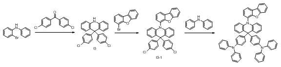
2-bromo-N-phenylaniline 10 g을 THF 100 ml에 녹인 후 반응 온도를 -78 ℃로 낮추고 BuLi 2.5 M을 20 ml 천천히 적가하고 1시간 동안 교반하였다. bis(4-chlorophenyl)methanone 15.2 g을 THF 150 ml에 녹인 후 천천히 적가한 후 실온으로 온도를 높이고 12시간 교반하였다. 반응이 종결된 후 증류수와 MC로 추출하고 무수황산마그네슘으로 물을 제거한 후 감압여과하여 얻은 고체를 더 이상의 정제 없이 Acetic acid 150 ml에 녹인 후 황산 10 ml를 적가하고 환류 교반하였다. 반응이 종결된 후 증류수와 MC로 추출하고 생성된 고체를 컬럼 정제하여 I3 10 g을 얻었다. (수율 62%)After dissolving 10 g of 2-bromo-N-phenylaniline in 100 ml of THF, the reaction temperature was lowered to -78 °C, and 20 ml of BuLi 2.5 M was slowly added dropwise and stirred for 1 hour. After dissolving 15.2 g of bis(4-chlorophenyl)methanone in 150 ml of THF, slowly added dropwise, the temperature was raised to room temperature, and the mixture was stirred for 12 hours. After the reaction was completed, the mixture was extracted with distilled water and MC, water was removed with anhydrous magnesium sulfate, and the solid obtained by filtration under reduced pressure was dissolved in 150 ml of Acetic acid without further purification, and 10 ml of sulfuric acid was added dropwise and stirred under reflux. After the reaction was completed, extraction was performed with distilled water and MC, and the resulting solid was purified by column to obtain 10 g of I 3 . (Yield 62%)
상기 단계의 I3 9 g, 4-bromodibenzo[b,d]furan 6.65 g, t-BuONa 3.2 g, Pd2(dba)3 0.8 g, (t-Bu)3P 1.1 ml를 톨루엔 200 ml에 녹인 후 환류 교반하였다. 반응이 종결되면 증류수와 EA로 추출한 후 컬럼정제하여 I3-1 11 g을 얻었다. (수율 59%)In the above step I 3 9 g, 4-bromodibenzo[b,d]furan 6.65 g, t-BuONa 3.2 g, Pd 2 (dba) 3 0.8 g, (t-Bu) 3 P 1.1 ml dissolved in 200 ml of toluene Then, the mixture was stirred under reflux. When the reaction was completed, extraction was performed with distilled water and EA, followed by column purification to obtain 11 g of I 3-1 . (Yield 59%)
상기 단계의 I3-1 10 g, diphenylamine 6.85 g, t-BuONa 2.5 g, Pd2(dba)3 0.6 g, (t-Bu)3P 1.6 ml를 톨루엔 200 ml에 녹인 후 환류 교반하였다. 반응이 종결되면 증류수와 EA로 추출한 후 컬럼정제하여 화합물 9 8 g을 얻었다. (수율 55%)I 3-1 of the above step 10 g, diphenylamine 6.85 g, t-BuONa 2.5 g, Pd 2 (dba) 3 0.6 g, (t-Bu) 3 P 1.6 ml was dissolved in 200 ml of toluene and stirred under reflux. When the reaction was completed, the mixture was extracted with distilled water and EA and purified by column to obtain 8 g of Compound 9. (Yield 55%)
m/z: 833.34 (100.0%), 834.34 (67.1%), 835.35 (21.8%), 836.35 (4.8%)
m/z: 833.34 (100.0%), 834.34 (67.1%), 835.35 (21.8%), 836.35 (4.8%)
[실시예 10: 화합물 10의 합성][Example 10: Synthesis of Compound 10]
diphenylamine을 9H-carbazole로 반응한 것을 제외하고는 화합물 9의 합성방법과 동일한 방법으로 하기 화합물 10을 얻었다.Except that diphenylamine was reacted with 9H-carbazole, the following
m/z: 829.31 (100.0%), 830.31 (67.1%), 831.32 (21.7%), 832.32 (4.8%)m/z: 829.31 (100.0%), 830.31 (67.1%), 831.32 (21.7%), 832.32 (4.8%)

[실시예 11: 화합물 11의 합성][Example 11: Synthesis of Compound 11]
bis(4-chlorophenyl)methanone을 2,7-dichloro-9H-fluoren-9-one으로 반응한 것을 제외하고는 화합물 9의 합성방법과 동일한 방법으로 하기 화합물 11을 얻었다.
m/z: 831.32 (100.0%), 832.33 (66.5%), 833.33 (22.7%), 834.34 (4.7%), 832.32 (1.1%)m/z: 831.32 (100.0%), 832.33 (66.5%), 833.33 (22.7%), 834.34 (4.7%), 832.32 (1.1%)
[실시예 12: 화합물 12의 합성][Example 12: Synthesis of Compound 12]
4-4-bromodibenzo[b,d]furan을 1-bromodibenzo[b,d]furan으로 반응한 것을 제외하고는 화합물 9의 합성방법과 동일한 방법으로 하기 화합물 12을 얻었다.Except for reacting 4-4-bromodibenzo[b,d]furan with 1-bromodibenzo[b,d]furan, the following
m/z: 833.34 (100.0%), 834.34 (67.1%), 835.35 (21.8%), 836.35 (4.8%)m/z: 833.34 (100.0%), 834.34 (67.1%), 835.35 (21.8%), 836.35 (4.8%)
[실시예 13: 화합물 13의 합성][Example 13: Synthesis of Compound 13]
diphenylamine을 9H-carbazole로 반응한 것을 제외하고는 화합물 12의 합성방법과 동일한 방법으로 하기 화합물 13을 얻었다.Except that diphenylamine was reacted with 9H-carbazole, the following
m/z: 829.31 (100.0%), 830.31 (67.1%), 831.32 (21.7%), 832.32 (4.8%)m/z: 829.31 (100.0%), 830.31 (67.1%), 831.32 (21.7%), 832.32 (4.8%)
[실시예 14: 화합물 14의 합성][Example 14: Synthesis of Compound 14]
4-4-bromodibenzo[b,d]furan을 1-bromodibenzo[b,d]furan으로 반응한 것을 제외하고는 화합물 11의 합성방법과 동일한 방법으로 하기 화합물 14를 얻었다.Except for reacting 4-4-bromodibenzo[b,d]furan with 1-bromodibenzo[b,d]furan, the following
m/z: 831.32 (100.0%), 832.33 (66.5%), 833.33 (22.7%), 834.34 (4.7%), 832.32 (1.1%)m/z: 831.32 (100.0%), 832.33 (66.5%), 833.33 (22.7%), 834.34 (4.7%), 832.32 (1.1%)

[실시예 15: 화합물 15의 합성][Example 15: Synthesis of Compound 15]

9,9-dimethyl-9,10-dihydroacridine 5 g, 4-bromodibenzo[b,d]thiophene 6.9 g, t-BuONa 3.5 g, Pd2(dba)3 0.9g, (t-Bu)3P 1.2 ml를 톨루엔 100 ml에 녹인후 환류 교반하였다. 반응이 종결되면 증류수와 EA로 추출한 후 컬럼정제하여 화합물 15를 얻었다. (수율 61%)9,9-dimethyl-9,10-dihydroacridine 5 g, 4-bromodibenzo[b,d]thiophene 6.9 g, t-BuONa 3.5 g, Pd 2 (dba) 3 0.9 g, (t-Bu) 3 P 1.2 ml Was dissolved in 100 ml of toluene and stirred under reflux. When the reaction was completed, the mixture was extracted with distilled water and EA, followed by column purification to obtain
m/z: 391.14 (100.0%), 392.14 (30.4%), 393.14 (4.9%), 393.15 (4.2%), 394.14 (1.3%)
m/z: 391.14 (100.0%), 392.14 (30.4%), 393.14 (4.9%), 393.15 (4.2%), 394.14 (1.3%)
[실시예 16: 화합물 16의 합성][Example 16: Synthesis of Compound 16]
4-4-bromodibenzo[b,d]furan을 4-bromodibenzo[b,d]thiophene으로 반응한 것을 제외하고는 화합물 2의 합성방법과 동일한 방법으로 하기 화합물 16을 얻었다.Except for reacting 4-4-bromodibenzo[b,d]furan with 4-bromodibenzo[b,d]thiophene, the following
m/z: 515.17 (100.0%), 516.17 (41.2%), 517.18 (7.9%), 517.17 (5.0%), 518.17 (1.9%), 518.18m/z: 515.17 (100.0%), 516.17 (41.2%), 517.18 (7.9%), 517.17 (5.0%), 518.17 (1.9%), 518.18

[실시예 17: 화합물 17의 합성][Example 17: Synthesis of Compound 17]
4-4-bromodibenzo[b,d]furan을 4-bromodibenzo[b,d]thiophene으로 반응한 것을 제외하고는 화합물 3의 합성방법과 동일한 방법으로 하기 화합물 17을 얻었다.Except for reacting 4-4-bromodibenzo[b,d]furan with 4-bromodibenzo[b,d]thiophene, the following compound 17 was obtained in the same manner as in the synthesis method of compound 3.
m/z: 513.16 (100.0%), 514.16 (40.3%), 515.16 (8.4%), 515.15 (4.5%), 516.15 (1.8%), 514.15 (1.2%), 516.17 (1.0%)m/z: 513.16 (100.0%), 514.16 (40.3%), 515.16 (8.4%), 515.15 (4.5%), 516.15 (1.8%), 514.15 (1.2%), 516.17 (1.0%)
[실시예 18: 화합물 18의 합성][Example 18: Synthesis of Compound 18]
4-4-bromodibenzo[b,d]furan을 2-bromo-9,9-dimethyl-9H-fluorene으로 반응한 것을 제외하고는 화합물 4의 합성방법과 동일한 방법으로 하기 화합물 18을 얻었다.Except for reacting 4-4-bromodibenzo[b,d]furan with 2-bromo-9,9-dimethyl-9H-fluorene, the following compound 18 was obtained in the same manner as the synthesis method of compound 4.

[실시예 19: 화합물 19의 합성][Example 19: Synthesis of Compound 19]
4-4-bromodibenzo[b,d]furan을 2-bromo-9,9-dimethyl-9H-fluorene으로 반응한 것을 제외하고는 화합물 2의 합성방법과 동일한 방법으로 하기 화합물 19를 얻었다.Except for reacting 4-4-bromodibenzo[b,d]furan with 2-bromo-9,9-dimethyl-9H-fluorene, the following compound 19 was obtained in the same manner as the synthesis method of
m/z: 525.25 (100.0%), 526.25 (43.6%), 527.25 (9.3%), 528.26 (1.3%)m/z: 525.25 (100.0%), 526.25 (43.6%), 527.25 (9.3%), 528.26 (1.3%)

[실시예 20: 화합물 20의 합성][Example 20: Synthesis of Compound 20]
4-4-bromodibenzo[b,d]furan을 2-bromo-9,9-dimethyl-9H-fluorene으로 반응한 것을 제외하고는 화합물 4의 합성방법과 동일한 방법으로 하기 화합물 20을 얻었다.Except for reacting 4-4-bromodibenzo[b,d]furan with 2-bromo-9,9-dimethyl-9H-fluorene, the following compound 20 was obtained in the same manner as the synthesis method of compound 4.

호스트를 이용한 유기발광소자의 제조Fabrication of organic light emitting device using host
도 1과 같은 구조로 유기발광소자를 제조하였다. 구체적으로 인듐틴옥사이드(ITO)가 1500 Å 두께가 박막 코팅된 유리 기판을 증류수 초음파로 세척하였다. 증류수 세척이 끝나면 이소프로필 알코올, 아세톤, 메탄올 등의 용제로 초음파 세척을 하고 건조시킨 후 플라즈마 세정기로 이송 시킨 다음 산소 플라즈마를 이용하여 상기 기판을 5분간 세정 한 후 ITO 기판 상부에 열 진공 증착기(thermal evaporator)를 이용하여 정공주입층으로 2-TNATA 600 Å, 정공전달층으로 NPB 200 Å를 제막하였다.An organic light-emitting device was manufactured with the structure shown in FIG. 1. Specifically, a glass substrate coated with a 1500 Å thick thin film of indium tin oxide (ITO) was washed with distilled water and ultrasonic waves. After washing with distilled water, ultrasonically clean with a solvent such as isopropyl alcohol, acetone, methanol, etc., dry, transfer to a plasma cleaner, and clean the substrate for 5 minutes using oxygen plasma, and then use a thermal vacuum evaporator on the top of the ITO substrate. evaporator) to form 2-TNATA 600 Å as a hole injection layer and NPB 200 Å as a hole transport layer.
다음으로 상기 실시예에서 합성한 실시예 1 내지 20의 호스트 물질을 Ir(ppy)3 7%로 도핑하여 300 Å 제막하였다. 다음으로 전자전달층으로 TPBi 300 Å 제막한 후 LiF 10 Å, 알루미늄(Al) 1000 Å 제막하고, 이 소자를 글로브 박스에서 밀봉(Encapsulation)함으로써 유기발광소자를 제작하였다.
Next, the host materials of Examples 1 to 20 synthesized in the above example were doped with 7% Ir (ppy) 3 to form a 300 Å film. Next, 300 Å of TPBi was formed as an electron transport layer, 10 Å of LiF and 1000 Å of aluminum (Al) were formed, and the device was encapsulated in a glove box to fabricate an organic light-emitting device.
정공수송층을Hole transport layer 이용한 유기발광소자의 제조 Fabrication of used organic light emitting device
인듐틴옥사이드(ITO)가 1500 Å 두께가 박막 코팅된 유리 기판을 증류수 초음파로 세척하였다. 증류수 세척이 끝나면 이소프로필 알코올, 아세톤, 메탄올 등의 용제로 초음파 세척을 하고 건조시킨 후 플라즈마 세정기로 이송 시킨 다음 산소 플라즈마를 이용하여 상기 기판을 5분간 세정 한 후 ITO 기판 상부에 열 진공 증착기(thermal evaporator)를 이용하여 정공주입층으로 2-TNATA 600 Å, 정공전달층으로 상기 실시예 1 내지 20에서 합성한 화합물 200 Å를 제막하였다. 다음으로 mCP를 Ir(ppy)3 7%로 도핑하여 300 Å 제막하였다. 다음으로 전자전달층으로 TPBi 300 Å 제막한후 LiF 10 Å, 알루미늄(Al) 1000 Å 제막하고, 이 소자를 글로브 박스에서 밀봉(Encapsulation)함으로써 유기발광소자를 제작하였다.
The glass substrate coated with indium tin oxide (ITO) having a thickness of 1500 Å was washed with distilled water and ultrasonic waves. After washing with distilled water, ultrasonically clean with a solvent such as isopropyl alcohol, acetone, methanol, etc., dry, transfer to a plasma cleaner, and clean the substrate for 5 minutes using oxygen plasma, and then use a thermal vacuum evaporator on the top of the ITO substrate. evaporator) was used as a hole injection layer to form a 2-TNATA 600 Å and a hole transport layer to form 200 Å of the compound synthesized in Examples 1 to 20. Next, mCP was doped with 7% Ir(ppy) 3 to form a 300 Å film. Next, TPBi 300 Å was formed as an electron transport layer,
비교예 : 정공수송층을 이용한 유기발광소자의 제조Comparative Example: Fabrication of an organic light emitting device using a hole transport layer
상기 실시예의 정공수송층과 발광층 호스트를 NPB와 mCP를 사용한 것을 제외하고는 동일한 방법으로 유기발광소자를 제작하였다.
An organic light-emitting device was fabricated in the same manner, except that NPB and mCP were used as the hole transport layer and the emission layer host of the above example.
유기발광소자의 성능평가Performance evaluation of organic light emitting device
키슬리 2400 소스 메져먼트 유닛(Kiethley 2400 source measurement unit) 으로 전압을 인가하여 전자 및 정공을 주입하고 코니카 미놀타(Konica Minolta) 분광복사계(CS-2000)를 이용하여 빛이 방출될 때의 휘도를 측정함으로써, 실시예 및 비교예의 유기발광소자의 성능을 인가전압에 대한 전류 밀도 및 휘도를 대기압 조건하에 측정하여 평가하였으며, 그 결과를 표 1에 나타내었다.A voltage is applied to the Keithley 2400 source measurement unit to inject electrons and holes, and the luminance when light is emitted is measured using a Konica Minolta spectroradiometer (CS-2000). By doing so, the performance of the organic light emitting device of Examples and Comparative Examples was evaluated by measuring the current density and luminance with respect to the applied voltage under atmospheric pressure conditions, and the results are shown in Table 1.
화합물1:Ir(ppy)3(7%) / TPBi / LiF / AlITO / 2-TNATA / NPB /
Compound 1: Ir(ppy)3(7%) / TPBi / LiF / Al
화합물2:Ir(ppy)3(7%) / TPBi / LiF / AlITO / 2-TNATA / NPB /
Compound 2: Ir(ppy)3(7%) / TPBi / LiF / Al
화합물3:Ir(ppy)3(7%) / TPBi / LiF / AlITO / 2-TNATA / NPB /
Compound 3: Ir(ppy)3(7%) / TPBi / LiF / Al
화합물4:Ir(ppy)3(7%) / TPBi / LiF / AlITO / 2-TNATA / NPB /
Compound 4: Ir(ppy)3(7%) / TPBi / LiF / Al
화합물5:Ir(ppy)3(7%) / TPBi / LiF / AlITO / 2-TNATA / NPB /
Compound 5: Ir(ppy)3(7%) / TPBi / LiF / Al
화합물6:Ir(ppy)3(7%) / TPBi / LiF / AlITO / 2-TNATA / NPB /
Compound 6: Ir(ppy)3(7%) / TPBi / LiF / Al
화합물7:Ir(ppy)3(7%) / TPBi / LiF / AlITO / 2-TNATA / NPB /
Compound 7: Ir(ppy)3(7%) / TPBi / LiF / Al
화합물8:Ir(ppy)3(7%) / TPBi / LiF / AlITO / 2-TNATA / NPB /
Compound 8: Ir(ppy)3(7%) / TPBi / LiF / Al
화합물10:Ir(ppy)3(7%) / TPBi / LiF / AlITO / 2-TNATA / NPB /
Compound 10: Ir(ppy)3(7%) / TPBi / LiF / Al
mCP:Ir(ppy)3(7%) / TPBi / LiF / AlITO / 2-TNATA / compound 9 /
mCP:Ir(ppy)3(7%) / TPBi / LiF / Al
mCP:Ir(ppy)3(7%) / TPBi / LiF / AlITO / 2-TNATA /
mCP:Ir(ppy)3(7%) / TPBi / LiF / Al
mCP:Ir(ppy)3(7%) / TPBi / LiF / AlITO / 2-TNATA /
mCP:Ir(ppy)3(7%) / TPBi / LiF / Al
mCP:Ir(ppy)3(7%) / TPBi / LiF / AlITO / 2-TNATA / NPB /
mCP:Ir(ppy)3(7%) / TPBi / LiF / Al
상기 표 1에 나타나는 바와 같이 본 발명에 따른 실시예 1 내지 11에서 합성한 화합물을 사용한 실시예 21 내지 32의 유기발광소자는 비교예에 비하여 휘도, 효율 및 전류밀도가 모두 우수함을 확인할 수 있다.As shown in Table 1, it can be seen that the organic light emitting devices of Examples 21 to 32 using the compounds synthesized in Examples 1 to 11 according to the present invention have superior luminance, efficiency, and current density compared to the comparative example.
Claims (11)
[화학식 1]
상기 식에서,
X는 치환 또는 비치환된 O, P, S, Se 또는 Si이고, X가 O일 경우 아크리딘의 질소 원자는 헤테로아릴계 모이어티의 3번 위치에는 결합될 수 없고;
R1 및 R2는 각각 독립적으로, 수소; 중수소; 중수소, 할로겐, 아미노기, 니트릴기, 니트로기로 치환되거나 치환되지 않은 C1-30의 알킬기; 중수소, 할로겐, 아미노기, 니트릴기, 니트로기로 치환되거나 치환되지 않은 C2-30의 알케닐기; 중수소, 할로겐, 아미노기, 니트릴기, 니트로기로 치환되거나 치환되지 않은 C2-30의 알키닐기; 중수소, 할로겐, 아미노기, 니트릴기, 니트로기로 치환되거나 치환되지 않은 C1-30의 알콕시기; 중수소, 할로겐, 아미노기, 니트릴기, 니트로기로 치환되거나 치환되지 않은 C6-30의 아릴옥시기; 중수소, 할로겐, 아미노기, 니트릴기, 니트로기로 치환되거나 치환되지 않은 C6-36의 아릴기; 또는 중수소, 할로겐, 아미노기, 니트릴기, 니트로기로 치환된 치환되거나 치환되지 않은 C2-36의 헤테로아릴기이고, 상기 R1 및 R2 는 서로 결합하여 포화 또는 불포화 탄소 고리를 형성할 수 있으며,
R3 내지 R17은 각각 독립적으로, 수소; 중수소; 중수소, 할로겐, 아미노기, 니트릴기, 니트로기로 치환되거나 치환되지 않은 C1-30의 알킬기; 중수소, 할로겐, 아미노기, 니트릴기, 니트로기로 치환되거나 치환되지 않은 C2-30의 알케닐기; 중수소, 할로겐, 아미노기, 니트릴기, 니트로기로 치환되거나 치환되지 않은 C2-30의 알키닐기; 중수소, 할로겐, 아미노기, 니트릴기, 니트로기로 치환되거나 치환되지 않은 C1-30의 알콕시기; 중수소, 할로겐, 아미노기, 니트릴기, 니트로기로 치환되거나 치환되지 않은 C6-30의 아릴옥시기; 중수소, 할로겐, 아미노기, 니트릴기, 니트로기로 치환되거나 치환되지 않은 C6-36의 아릴기이다.An organic light-emitting compound comprising an acridine derivative represented by the following formula (1):
[Formula 1]
In the above formula,
X is a substituted or unsubstituted O, P, S, Se or Si, and when X is O, the nitrogen atom of acridine cannot be bonded to the 3rd position of the heteroaryl-based moiety;
R 1 and R 2 are each independently hydrogen; heavy hydrogen; C 1-30 alkyl group substituted or unsubstituted with deuterium, halogen, amino group, nitrile group, nitro group; C 2-30 alkenyl group substituted or unsubstituted with deuterium, halogen, amino group, nitrile group, nitro group; C 2-30 alkynyl group substituted or unsubstituted with deuterium, halogen, amino group, nitrile group, nitro group; C 1-30 alkoxy group substituted or unsubstituted with deuterium, halogen, amino group, nitrile group, nitro group; C 6-30 aryloxy group substituted or unsubstituted with deuterium, halogen, amino group, nitrile group, nitro group; C 6-36 aryl group substituted or unsubstituted with deuterium, halogen, amino group, nitrile group, nitro group; Or a substituted or unsubstituted C 2-36 heteroaryl group substituted with deuterium, halogen, amino group, nitrile group, nitro group, and R 1 and R 2 may be bonded to each other to form a saturated or unsaturated carbon ring,
R 3 to R 17 are each independently hydrogen; heavy hydrogen; C 1-30 alkyl group substituted or unsubstituted with deuterium, halogen, amino group, nitrile group, nitro group; C 2-30 alkenyl group substituted or unsubstituted with deuterium, halogen, amino group, nitrile group, nitro group; C 2-30 alkynyl group substituted or unsubstituted with deuterium, halogen, amino group, nitrile group, nitro group; C 1-30 alkoxy group substituted or unsubstituted with deuterium, halogen, amino group, nitrile group, nitro group; C 6-30 aryloxy group substituted or unsubstituted with deuterium, halogen, amino group, nitrile group, nitro group; It is a C 6-36 aryl group substituted or unsubstituted with deuterium, halogen, amino group, nitrile group, and nitro group.
상기 화학식 1의 화합물이 중수소로 치환되는 경우, 적어도 20%로 중수소화 되는 것을 특징으로 하는 유기발광 화합물.The method of claim 1,
When the compound of Formula 1 is substituted with deuterium, the organic light emitting compound is deuterated to at least 20%.
상기 아크리딘계 모이어티(moiety)의 질소 원자에 직접 연결된 아릴계 또는 헤테로아릴계 모이어티가 중수소로 치환되는 경우에는, 적어도 50% 중수소화 되는 것을 특징으로 하는 유기발광 화합물.The method of claim 1,
When the aryl-based or heteroaryl-based moiety directly connected to the nitrogen atom of the acridine-based moiety is substituted with deuterium, the organic light-emitting compound is at least 50% deuterated.


상기 유기물층이 정공주입층, 정공수송층, 발광층, 전자수송층 및 전자주입층으로 이루어진 군에서 선택되는 하나 이상인 것을 특징으로 하는 유기발광소자.The method of claim 7,
The organic light emitting device, wherein the organic material layer is at least one selected from the group consisting of a hole injection layer, a hole transport layer, a light emitting layer, an electron transport layer, and an electron injection layer.
상기 정공주입층, 정공수송층, 발광층, 전자수송층 및 전자주입층이 각각 10 내지 1,000 ㎚의 두께를 갖는 것을 특징으로 하는 유기발광소자.The method of claim 8,
The organic light emitting device, characterized in that the hole injection layer, the hole transport layer, the light emitting layer, the electron transport layer and the electron injection layer each have a thickness of 10 to 1,000 nm.
상기 유기물층이 제1항의 화합물을 발광 호스트 또는 도펀트로서 함유하는 것을 특징으로 하는 유기발광소자.The method of claim 7,
An organic light-emitting device, wherein the organic material layer contains the compound of claim 1 as a light emitting host or a dopant.
상기 도펀트가 호스트 100 중량부 대비 0.01 내지 15 중량부의 양으로 첨가되는 것을 특징으로 하는 유기발광소자.The method of claim 10,
An organic light-emitting device, characterized in that the dopant is added in an amount of 0.01 to 15 parts by weight based on 100 parts by weight of the host.
Priority Applications (2)
| Application Number | Priority Date | Filing Date | Title |
|---|---|---|---|
| PCT/KR2013/006669 WO2014017844A1 (en) | 2012-07-26 | 2013-07-25 | Organic light-emitting compound comprising acridine derivatives, and organic light-emitting device comprising same |
| CN201380038477.2A CN104471022B (en) | 2012-07-26 | 2013-07-25 | Organic light-emitting compound containing acridine derivative and organic light-emitting device containing the organic light-emitting compound |
Applications Claiming Priority (2)
| Application Number | Priority Date | Filing Date | Title |
|---|---|---|---|
| KR1020120081797 | 2012-07-26 | ||
| KR20120081797 | 2012-07-26 |
Publications (2)
| Publication Number | Publication Date |
|---|---|
| KR20140015202A KR20140015202A (en) | 2014-02-06 |
| KR102169273B1 true KR102169273B1 (en) | 2020-10-23 |
Family
ID=50264917
Family Applications (1)
| Application Number | Title | Priority Date | Filing Date |
|---|---|---|---|
| KR1020130087572A Active KR102169273B1 (en) | 2012-07-26 | 2013-07-24 | Organic electroluminescent compound comprising acridine derivative and organic electroluminescent device comprising same |
Country Status (2)
| Country | Link |
|---|---|
| KR (1) | KR102169273B1 (en) |
| CN (1) | CN104471022B (en) |
Families Citing this family (14)
| Publication number | Priority date | Publication date | Assignee | Title |
|---|---|---|---|---|
| KR102429520B1 (en) * | 2014-04-29 | 2022-08-05 | 주식회사 동진쎄미켐 | Novel compound and organic electroluminescent device comprising same |
| EP3180411B1 (en) * | 2014-08-13 | 2018-08-29 | Merck Patent GmbH | Materials for organic electroluminescent devices |
| US10547008B2 (en) * | 2015-06-19 | 2020-01-28 | Lg Chem, Ltd. | Organic light emitting device |
| CN105254561A (en) * | 2015-11-10 | 2016-01-20 | 江苏三月光电科技有限公司 | Organic compound used for OLED and containing fluorene and application thereof |
| JP7073388B2 (en) * | 2016-11-08 | 2022-05-23 | メルク パテント ゲーエムベーハー | Compounds for electronic devices |
| KR102667321B1 (en) * | 2016-12-13 | 2024-05-17 | 엘지디스플레이 주식회사 | Organic compounds, organic light emitting diode and orgnic light emitting diode display device having the compounds |
| KR102508497B1 (en) | 2018-03-26 | 2023-03-10 | 삼성디스플레이 주식회사 | Heterocyclic compound and organic light emitting device comprising the same |
| KR102719524B1 (en) | 2018-12-10 | 2024-10-22 | 삼성디스플레이 주식회사 | Organic electroluminescence device and polycyclic compound for organic electroluminescence device |
| KR102745916B1 (en) | 2018-12-10 | 2024-12-26 | 삼성디스플레이 주식회사 | Organic electroluminescence device and polycyclic compound for organic electroluminescence device |
| KR20200139287A (en) | 2019-06-03 | 2020-12-14 | 삼성디스플레이 주식회사 | Organic electroluminescence device and fused polycyclic compound for organic electroluminescence device |
| CN110204567B (en) * | 2019-06-04 | 2020-12-04 | 武汉华星光电半导体显示技术有限公司 | Organic compound, application thereof and organic light-emitting diode electroluminescent device |
| TW202110808A (en) * | 2019-06-27 | 2021-03-16 | 日商關東化學股份有限公司 | A spiroacridane-based compound, a hole transport material including the same, and an organic electronic device including the same in a hole transport layer |
| CN111233764B (en) * | 2020-03-31 | 2022-03-18 | 烟台显华化工科技有限公司 | Organic compound with acridine derived triarylamine structure and application thereof |
| CN116621778A (en) * | 2022-04-29 | 2023-08-22 | 北京华森英诺生物科技有限公司 | USP inhibitor, its preparation method and application |
Citations (4)
| Publication number | Priority date | Publication date | Assignee | Title |
|---|---|---|---|---|
| JP2010059147A (en) * | 2008-07-14 | 2010-03-18 | Gracel Display Inc | New organic electric field luminescent compound, and organic electric field luminescent element by using the same |
| JP2011210749A (en) * | 2010-03-26 | 2011-10-20 | Fujifilm Corp | Organic electroluminescent element and charge transport material |
| WO2012034627A1 (en) * | 2010-09-15 | 2012-03-22 | Merck Patent Gmbh | Materials for organic electroluminescent devices |
| WO2012049828A1 (en) * | 2010-10-12 | 2012-04-19 | 出光興産株式会社 | Aromatic heterocyclic derivative, and organic electroluminescent element comprising same |
Family Cites Families (9)
| Publication number | Priority date | Publication date | Assignee | Title |
|---|---|---|---|---|
| US6579630B2 (en) * | 2000-12-07 | 2003-06-17 | Canon Kabushiki Kaisha | Deuterated semiconducting organic compounds used for opto-electronic devices |
| KR20090048299A (en) * | 2007-11-08 | 2009-05-13 | 주식회사 엘지화학 | New organic light emitting device material and organic light emitting device using same |
| KR20100069216A (en) * | 2008-12-16 | 2010-06-24 | 주식회사 두산 | Deuterated anthracene derivative and organic light emitting device comprising the same |
| KR101779913B1 (en) * | 2010-04-01 | 2017-09-20 | 에스에프씨 주식회사 | Spiro compound and organic electroluminescent devices comprising the same |
| KR101791022B1 (en) * | 2010-04-02 | 2017-10-30 | 에스에프씨 주식회사 | spiro compounds and organic light-emitting diode including the same |
| WO2012029253A1 (en) * | 2010-08-31 | 2012-03-08 | 出光興産株式会社 | Nitrogen-containing aromatic heterocyclic derivative and organic electroluminescence device using same |
| KR20120083242A (en) * | 2011-01-17 | 2012-07-25 | 주식회사 엘지화학 | New compounds and organic light emitting device comprising the same |
| CN103619821A (en) * | 2011-04-27 | 2014-03-05 | 保土谷化学工业株式会社 | Compound with 9,10-dihydroacridine ring structure and organic electroluminescent device |
| KR101375360B1 (en) * | 2011-06-30 | 2014-03-20 | (주)씨에스엘쏠라 | Organic light compound and organic light device using the same |
-
2013
- 2013-07-24 KR KR1020130087572A patent/KR102169273B1/en active Active
- 2013-07-25 CN CN201380038477.2A patent/CN104471022B/en active Active
Patent Citations (4)
| Publication number | Priority date | Publication date | Assignee | Title |
|---|---|---|---|---|
| JP2010059147A (en) * | 2008-07-14 | 2010-03-18 | Gracel Display Inc | New organic electric field luminescent compound, and organic electric field luminescent element by using the same |
| JP2011210749A (en) * | 2010-03-26 | 2011-10-20 | Fujifilm Corp | Organic electroluminescent element and charge transport material |
| WO2012034627A1 (en) * | 2010-09-15 | 2012-03-22 | Merck Patent Gmbh | Materials for organic electroluminescent devices |
| WO2012049828A1 (en) * | 2010-10-12 | 2012-04-19 | 出光興産株式会社 | Aromatic heterocyclic derivative, and organic electroluminescent element comprising same |
Also Published As
| Publication number | Publication date |
|---|---|
| CN104471022B (en) | 2018-02-06 |
| KR20140015202A (en) | 2014-02-06 |
| CN104471022A (en) | 2015-03-25 |
Similar Documents
| Publication | Publication Date | Title |
|---|---|---|
| KR102160946B1 (en) | Organic electroluminescent compound comprising acridine derivative and organic electroluminescent device comprising same | |
| KR102169273B1 (en) | Organic electroluminescent compound comprising acridine derivative and organic electroluminescent device comprising same | |
| KR102559622B1 (en) | Novel compound and organic electroluminescent device comprising same | |
| KR20240149861A (en) | Novel compound and organic electroluminescent device comprising same | |
| KR101996649B1 (en) | Pyrene derivative compounds and organic light-emitting diode including the same | |
| KR101983991B1 (en) | Condensed aryl compound and organic light-diode including the same | |
| KR102671576B1 (en) | Novel compound and organic electroluminescent device comprising same | |
| KR102423699B1 (en) | Novel compound and organic electroluminescent device comprising same | |
| KR102659372B1 (en) | Novel compound and organic electroluminescent device comprising the same | |
| KR20140086880A (en) | Novel organic compound and organic electroluminescent device comprising same | |
| KR102402220B1 (en) | Novel blue fluorescent host compound and organic electroluminescent device comprising same | |
| KR102387855B1 (en) | Novel electroluminescent compound and organic electroluminescent device comprising same | |
| KR102448875B1 (en) | Novel compound and organic light emitting device comprising same | |
| KR20180020577A (en) | Novel compound and organic electroluminescent device comprising the same | |
| KR102394380B1 (en) | Novel electroluminescent compound and organic electroluminescent device comprising same | |
| KR101555155B1 (en) | Novel spyrobifluorene type organic compounds and an organic electroluminescent device comprising the same | |
| KR20140081735A (en) | Novel organic electroluminescent compound substituted with deuterium and organic electroluminescent device comprising same | |
| KR102429520B1 (en) | Novel compound and organic electroluminescent device comprising same | |
| KR102630946B1 (en) | Novel compound and organic electroluminescent device comprising same | |
| KR102630325B1 (en) | Novel compound and organic electroluminescent device comprising the same | |
| KR102447718B1 (en) | Novel light emitting compound and organic light emitting device comprising same | |
| KR102245921B1 (en) | Novel organic compound and organic electroluminescent device comprising same | |
| KR102437956B1 (en) | Novel compound and organic light emitting device comprising same | |
| KR20180041477A (en) | Novel compound and organic electroluminescent device comprising the same | |
| KR20170052777A (en) | Novel compound and organic electroluminescent device comprising same |
Legal Events
| Date | Code | Title | Description |
|---|---|---|---|
| PA0109 | Patent application |
St.27 status event code: A-0-1-A10-A12-nap-PA0109 |
|
| PG1501 | Laying open of application |
St.27 status event code: A-1-1-Q10-Q12-nap-PG1501 |
|
| R18-X000 | Changes to party contact information recorded |
St.27 status event code: A-3-3-R10-R18-oth-X000 |
|
| R17-X000 | Change to representative recorded |
St.27 status event code: A-3-3-R10-R17-oth-X000 |
|
| A201 | Request for examination | ||
| PA0201 | Request for examination |
St.27 status event code: A-1-2-D10-D11-exm-PA0201 |
|
| E902 | Notification of reason for refusal | ||
| PE0902 | Notice of grounds for rejection |
St.27 status event code: A-1-2-D10-D21-exm-PE0902 |
|
| T11-X000 | Administrative time limit extension requested |
St.27 status event code: U-3-3-T10-T11-oth-X000 |
|
| E13-X000 | Pre-grant limitation requested |
St.27 status event code: A-2-3-E10-E13-lim-X000 |
|
| P11-X000 | Amendment of application requested |
St.27 status event code: A-2-2-P10-P11-nap-X000 |
|
| P13-X000 | Application amended |
St.27 status event code: A-2-2-P10-P13-nap-X000 |
|
| E701 | Decision to grant or registration of patent right | ||
| PE0701 | Decision of registration |
St.27 status event code: A-1-2-D10-D22-exm-PE0701 |
|
| GRNT | Written decision to grant | ||
| PR0701 | Registration of establishment |
St.27 status event code: A-2-4-F10-F11-exm-PR0701 |
|
| PR1002 | Payment of registration fee |
St.27 status event code: A-2-2-U10-U11-oth-PR1002 Fee payment year number: 1 |
|
| PG1601 | Publication of registration |
St.27 status event code: A-4-4-Q10-Q13-nap-PG1601 |
|
| P22-X000 | Classification modified |
St.27 status event code: A-4-4-P10-P22-nap-X000 |
|
| P22-X000 | Classification modified |
St.27 status event code: A-4-4-P10-P22-nap-X000 |
|
| P22-X000 | Classification modified |
St.27 status event code: A-4-4-P10-P22-nap-X000 |
|
| PR1001 | Payment of annual fee |
St.27 status event code: A-4-4-U10-U11-oth-PR1001 Fee payment year number: 4 |
|
| PR1001 | Payment of annual fee |
St.27 status event code: A-4-4-U10-U11-oth-PR1001 Fee payment year number: 5 |
|
| PR1001 | Payment of annual fee |
St.27 status event code: A-4-4-U10-U11-oth-PR1001 Fee payment year number: 6 |
|
| U11 | Full renewal or maintenance fee paid |
Free format text: ST27 STATUS EVENT CODE: A-4-4-U10-U11-OTH-PR1001 (AS PROVIDED BY THE NATIONAL OFFICE) Year of fee payment: 6 |
|
| P22-X000 | Classification modified |
St.27 status event code: A-4-4-P10-P22-nap-X000 |