KR102150007B1 - Passivation structure of multi-stage surface and manufacturing method thereof - Google Patents
Passivation structure of multi-stage surface and manufacturing method thereof Download PDFInfo
- Publication number
- KR102150007B1 KR102150007B1 KR1020187037936A KR20187037936A KR102150007B1 KR 102150007 B1 KR102150007 B1 KR 102150007B1 KR 1020187037936 A KR1020187037936 A KR 1020187037936A KR 20187037936 A KR20187037936 A KR 20187037936A KR 102150007 B1 KR102150007 B1 KR 102150007B1
- Authority
- KR
- South Korea
- Prior art keywords
- insulator
- layer
- disposed
- gate
- contact
- Prior art date
- Legal status (The legal status is an assumption and is not a legal conclusion. Google has not performed a legal analysis and makes no representation as to the accuracy of the status listed.)
- Active
Links
Images


Classifications
-
- H—ELECTRICITY
- H10—SEMICONDUCTOR DEVICES; ELECTRIC SOLID-STATE DEVICES NOT OTHERWISE PROVIDED FOR
- H10D—INORGANIC ELECTRIC SEMICONDUCTOR DEVICES
- H10D30/00—Field-effect transistors [FET]
- H10D30/40—FETs having zero-dimensional [0D], one-dimensional [1D] or two-dimensional [2D] charge carrier gas channels
- H10D30/47—FETs having zero-dimensional [0D], one-dimensional [1D] or two-dimensional [2D] charge carrier gas channels having 2D charge carrier gas channels, e.g. nanoribbon FETs or high electron mobility transistors [HEMT]
- H10D30/471—High electron mobility transistors [HEMT] or high hole mobility transistors [HHMT]
- H10D30/475—High electron mobility transistors [HEMT] or high hole mobility transistors [HHMT] having wider bandgap layer formed on top of lower bandgap active layer, e.g. undoped barrier HEMTs such as i-AlGaN/GaN HEMTs
- H10D30/4755—High electron mobility transistors [HEMT] or high hole mobility transistors [HHMT] having wider bandgap layer formed on top of lower bandgap active layer, e.g. undoped barrier HEMTs such as i-AlGaN/GaN HEMTs having wide bandgap charge-carrier supplying layers, e.g. modulation doped HEMTs such as n-AlGaAs/GaAs HEMTs
-
- H01L29/7787—
-
- H—ELECTRICITY
- H01—ELECTRIC ELEMENTS
- H01L—SEMICONDUCTOR DEVICES NOT COVERED BY CLASS H10
- H01L23/00—Details of semiconductor or other solid state devices
- H01L23/28—Encapsulations, e.g. encapsulating layers, coatings, e.g. for protection
- H01L23/31—Encapsulations, e.g. encapsulating layers, coatings, e.g. for protection characterised by the arrangement or shape
- H01L23/3157—Partial encapsulation or coating
- H01L23/3171—Partial encapsulation or coating the coating being directly applied to the semiconductor body, e.g. passivation layer
-
- H01L29/1066—
-
- H01L29/2003—
-
- H01L29/205—
-
- H01L29/402—
-
- H01L29/513—
-
- H01L29/66462—
-
- H—ELECTRICITY
- H10—SEMICONDUCTOR DEVICES; ELECTRIC SOLID-STATE DEVICES NOT OTHERWISE PROVIDED FOR
- H10D—INORGANIC ELECTRIC SEMICONDUCTOR DEVICES
- H10D30/00—Field-effect transistors [FET]
- H10D30/01—Manufacture or treatment
- H10D30/015—Manufacture or treatment of FETs having heterojunction interface channels or heterojunction gate electrodes, e.g. HEMT
-
- H—ELECTRICITY
- H10—SEMICONDUCTOR DEVICES; ELECTRIC SOLID-STATE DEVICES NOT OTHERWISE PROVIDED FOR
- H10D—INORGANIC ELECTRIC SEMICONDUCTOR DEVICES
- H10D30/00—Field-effect transistors [FET]
- H10D30/40—FETs having zero-dimensional [0D], one-dimensional [1D] or two-dimensional [2D] charge carrier gas channels
- H10D30/47—FETs having zero-dimensional [0D], one-dimensional [1D] or two-dimensional [2D] charge carrier gas channels having 2D charge carrier gas channels, e.g. nanoribbon FETs or high electron mobility transistors [HEMT]
- H10D30/471—High electron mobility transistors [HEMT] or high hole mobility transistors [HHMT]
- H10D30/475—High electron mobility transistors [HEMT] or high hole mobility transistors [HHMT] having wider bandgap layer formed on top of lower bandgap active layer, e.g. undoped barrier HEMTs such as i-AlGaN/GaN HEMTs
-
- H—ELECTRICITY
- H10—SEMICONDUCTOR DEVICES; ELECTRIC SOLID-STATE DEVICES NOT OTHERWISE PROVIDED FOR
- H10D—INORGANIC ELECTRIC SEMICONDUCTOR DEVICES
- H10D62/00—Semiconductor bodies, or regions thereof, of devices having potential barriers
- H10D62/10—Shapes, relative sizes or dispositions of the regions of the semiconductor bodies; Shapes of the semiconductor bodies
- H10D62/17—Semiconductor regions connected to electrodes not carrying current to be rectified, amplified or switched, e.g. channel regions
- H10D62/343—Gate regions of field-effect devices having PN junction gates
-
- H—ELECTRICITY
- H10—SEMICONDUCTOR DEVICES; ELECTRIC SOLID-STATE DEVICES NOT OTHERWISE PROVIDED FOR
- H10D—INORGANIC ELECTRIC SEMICONDUCTOR DEVICES
- H10D62/00—Semiconductor bodies, or regions thereof, of devices having potential barriers
- H10D62/80—Semiconductor bodies, or regions thereof, of devices having potential barriers characterised by the materials
- H10D62/82—Heterojunctions
- H10D62/824—Heterojunctions comprising only Group III-V materials heterojunctions, e.g. GaN/AlGaN heterojunctions
-
- H—ELECTRICITY
- H10—SEMICONDUCTOR DEVICES; ELECTRIC SOLID-STATE DEVICES NOT OTHERWISE PROVIDED FOR
- H10D—INORGANIC ELECTRIC SEMICONDUCTOR DEVICES
- H10D62/00—Semiconductor bodies, or regions thereof, of devices having potential barriers
- H10D62/80—Semiconductor bodies, or regions thereof, of devices having potential barriers characterised by the materials
- H10D62/85—Semiconductor bodies, or regions thereof, of devices having potential barriers characterised by the materials being Group III-V materials, e.g. GaAs
- H10D62/8503—Nitride Group III-V materials, e.g. AlN or GaN
-
- H—ELECTRICITY
- H10—SEMICONDUCTOR DEVICES; ELECTRIC SOLID-STATE DEVICES NOT OTHERWISE PROVIDED FOR
- H10D—INORGANIC ELECTRIC SEMICONDUCTOR DEVICES
- H10D64/00—Electrodes of devices having potential barriers
- H10D64/111—Field plates
-
- H—ELECTRICITY
- H10—SEMICONDUCTOR DEVICES; ELECTRIC SOLID-STATE DEVICES NOT OTHERWISE PROVIDED FOR
- H10D—INORGANIC ELECTRIC SEMICONDUCTOR DEVICES
- H10D64/00—Electrodes of devices having potential barriers
- H10D64/60—Electrodes characterised by their materials
- H10D64/66—Electrodes having a conductor capacitively coupled to a semiconductor by an insulator, e.g. MIS electrodes
- H10D64/68—Electrodes having a conductor capacitively coupled to a semiconductor by an insulator, e.g. MIS electrodes characterised by the insulator, e.g. by the gate insulator
- H10D64/681—Electrodes having a conductor capacitively coupled to a semiconductor by an insulator, e.g. MIS electrodes characterised by the insulator, e.g. by the gate insulator having a compositional variation, e.g. multilayered
- H10D64/685—Electrodes having a conductor capacitively coupled to a semiconductor by an insulator, e.g. MIS electrodes characterised by the insulator, e.g. by the gate insulator having a compositional variation, e.g. multilayered being perpendicular to the channel plane
-
- H10W74/137—
Landscapes
- Junction Field-Effect Transistors (AREA)
- Physics & Mathematics (AREA)
- Condensed Matter Physics & Semiconductors (AREA)
- General Physics & Mathematics (AREA)
- Engineering & Computer Science (AREA)
- Computer Hardware Design (AREA)
- Microelectronics & Electronic Packaging (AREA)
- Power Engineering (AREA)
- Insulated Gate Type Field-Effect Transistor (AREA)
Abstract
2개 이상의 절연체 반도체 계면 영역을 포함하는 갈륨 나이트라이드(GaN) 트랜지스터. 게이트와 드레인 사이(게이트 근처)에 배치된 제 1 절연체는 높은 게이트-드레인 전하(![]()
![]()
Description
본 발명은 갈륨 나이트라이드(GaN) 트랜지스터와 같은 III족 질화물 트랜지스터 분야에 관한 것이다. 특히, 본 발명은 다중 절연체 반도체 인터페이스 영역을 갖는 GaN 트랜지스터에 관한 것이다.The present invention relates to the field of group III nitride transistors, such as gallium nitride (GaN) transistors. In particular, the present invention relates to a GaN transistor having multiple insulator semiconductor interface regions.
갈륨 나이트라이드(GaN) 반도체 장치는, 대전류를 흘려보내고 고압을 지지하는 능력 때문에 전력(power) 반도체 장치에 점점 더 선호된다. 이러한 장치의 개발은, 일반적으로 고전력/고주파 애플리케이션(applications)을 목표로 하여 왔다. 이러한 종류의 애플리케이션을 위해 제조된 장치는, 고 전자 이동도(high electron mobility)를 나타내는 일반적인 장치 구조를 기반으로 하며, 헤테로정션 필드 이펙트 트랜지스터(heterojunction field effect transistors; HFET), 하이 일렉트론 모빌리티 트랜지스터(high electron mobility transistors; HEMT), 또는 모듈레이션 도프드 필드 이펙트 트랜지스터(modulation doped field effect transistors; MODFET)로 다양하게 불린다.Gallium nitride (GaN) semiconductor devices are increasingly preferred for power semiconductor devices because of their ability to pass large currents and support high voltages. The development of such devices has generally been aimed at high power/high frequency applications. Devices fabricated for this kind of application are based on typical device structures that exhibit high electron mobility, and include heterojunction field effect transistors (HFETs), high electron mobility transistors (high-electron mobility transistors). It is variously referred to as electron mobility transistors (HEMT), or modulation doped field effect transistors (MODFET).
GaN HEMT 장치는, 2개 이상의 나이트라이드층을 구비한 나이트라이드 반도체를 포함한다. 반도체 위에 또는 완충층(buffer layer) 위에 형성된 상이한 물질은, 나이트라이드층이 상이한 밴드갭(band gaps)을 갖게 한다. 또한, 인접하는 나이트라이드층의 상이한 물질은, 분극(polarization)을 야기하는데, 이는 2개 층, 특히 밴드갭(band gap)이 더 좁은 층의 접합 근처에, 도전성의 2차원 전자 가스(two dimensional electron gas: 2DEG) 영역을 초래한다.The GaN HEMT device includes a nitride semiconductor having two or more nitride layers. Different materials formed over the semiconductor or over the buffer layer cause the nitride layer to have different band gaps. In addition, different materials of adjacent nitride layers cause polarization, which is near the junction of two layers, especially a layer with a narrower band gap, of a conductive two dimensional electron gas. electron gas: 2DEG) region.
분극을 야기하는 나이트라이드층은, 일반적으로, 장치를 통과하여 전하(charge)를 흐르게 해주는 2DEG 영역을 포함하는 GaN의 층에 인접한 AlGaN의 배리어층을 포함한다. 이러한 배리어층은, 도핑되거나 미도핑될 수 있다. 제로(0)의 게이트 바이어스(gate bias)에서 2DEG 영역이 게이트 아래에 존재하기 때문에, 대부분의 나이트라이드 장치는 일반적으로, 온(on) 또는 디플리션형(depletion mode) 장치이다. 제로(0)가 인가되는 게이트 바이어스에서, 2DEG 영역이 게이트 아래에서 디플리트(deplete) 즉, 제거되면, 장치는 인핸스먼트형 장치가 될 수 있다. 인핸스먼트형 장치는, 일반적으로 오프(off) 상태이며, 장치가 더 높은 안전성을 제공하고, 장치가, 간단하고 저렴한 구동회로로 제어하는데 보다 용이하기 때문에 바람직하다. 인핸스먼트형 장치는, 전류를 흘려보내기 위하여, 게이트에 양(positive)의 바이어스를 인가하는 것이 필요하다.The nitride layer that causes polarization generally comprises a barrier layer of AlGaN adjacent to the layer of GaN that includes a 2DEG region that allows charge to flow through the device. This barrier layer may be doped or undoped. Since the 2DEG region exists under the gate at a gate bias of zero (0), most nitride devices are generally on or depletion mode devices. In a gate bias to which zero (0) is applied, if the 2DEG region is depleted, i.e. removed, under the gate, the device can be an enhancement type device. The enhancement type device is generally in the off state, the device provides higher safety, and the device is preferred because it is easier to control with a simple and inexpensive drive circuit. In the enhancement type device, it is necessary to apply a positive bias to the gate in order to pass current.
도 1은, 단일층의 표면 패시베이션 절연체(층)(108)을 갖는 인핸스먼트형 GaN 트랜지스터 장치(100)를 나타내고, 이는 Ueda 등의 미국 특허 8076698호에 보다 상세히 기술되어 있다. 도 1의 장치(100)는, 실리콘(Si), 실리콘 카바이드(SiC), 사파이어(sapphire) 또는 다른 물질로 구성될 수 있는 기판(101), 두께가 약 0.1㎛ 내지 약 1.0㎛ 되는, AlN과 AlGaN로 일반적으로 구성된 천이층(transition layer)(102), 두께가 약 0.5㎛ 내지 약 10㎛ 되는, GaN로 일반적으로 구성된 완충 물질(buffer material)(103), 두께가 약 0.005㎛ 내지 약 0.03㎛ 되는, Al 대 Ga 비율이 약 0.1 내지 약 0.5인 AlGaN로 일반적으로 구성된 배리어 물질(barrier material)(104), 피(p)형 AlGaN(105), 고 도핑 p형 GaN(106), 아이솔레이션 영역(isolation region)(107), 패시베이션 영역(passivation region)(108), Ni과 Au와 같은 캡핑(capping) 금속을 구비하는 Ti와 Al로 일반적으로 구성된, 소스(source)와 드레인(drain)을 위한 오믹 콘택 금속(ohmic contact metal)(109,110), 및 p형 GaN 게이트 위의 니켈(Ni)과 금(Au) 금속 콘택으로 일반적으로 구성된 게이트 금속(111)을 포함한다.1 shows an enhancement type
도 2는 표면 페시베이션 절연체를 갖지 않는 종래 GaN 트랜지스터 장치의 단면을 나타내고, 이는 Lidow 등의 미국 특허 8350294호에 보다 상세히 기술되어 있다. GaN 트랜지스터(1)는 예를 들어 실리콘(Si), 실리콘 카바이드(SiC) 또는 사파이어를 포함할 수 있는 기판(31) 상에 형성된다. 천이층은 두께가 약 0.1㎛ 내지 약 1.0㎛ 되고 AlN과 AlGaN로 일반적으로 구성된다. 버퍼층(33)은 천이층(32)을 배리어층(34)으로부터 분리시킨다. 버퍼층(33)은 바람직하게 In 및 Al의 임의의 농도 (0% In 및/또는 Al 포함)의 InAlGaN으로 형성되고 0.5㎛ 내지 3㎛의 두께를 갖는다. 배리어층은 AlGaN으로 형성되고 0.005㎛ 내지 0.03㎛의 두께 및 약 10% 내지 50%의 Al 퍼센티지를 갖는다. 소스 및 드레인 콘택(35, 36)은 배리어층 위에 있다. 소스 및 드레인 콘택은 Ni 또는 Au 또는 Ti 및 TiN과 같은 캡핑 금속으로 Ti 또는 Al로 형성된다. Ta, Ti, TiN, W 또는 WSi2로 이루어지고, 0.05㎛ 내지 1㎛의 두께를 갖는 게이트 콘택(37)은 소스 및 드레인 콘택 사이에 제공된다. 보정된 반도체층(38)은 배리어층(34) 위에 그리고 게이트 콘택(37) 아래에 형성된다. 보상된 반도체층(38)은 바람직하게 예를 들어 Mg, Zn, Be, Cd와 같은 깊은 레벨로 페시베이션 된 p형 불순물을 갖는 AlGaN 또는 GaN, 또는 Ca를 포함한다. 버퍼층(33) 및 배리어층(34)은 x+y ≤ 1 인 InxAlyGa(1-x-y)N 과 같은 III족 질화물 물질로 만들어진다. 보상층(38)의 높은 도핑 레벨은 인핸스먼트 모드 장치로 이어진다. 또한, 보상된 반도체층(38)은 장치의 작동동안 적은 게이트 누설을 야기하고, 마지막으로 보상된층의 절연 특성은 소자의 게이트 커패시턴스를 감소시킨다.2 shows a cross-section of a conventional GaN transistor device without a surface passivation insulator, which is described in more detail in U.S. Patent 8350294 to Lidow et al. The
도 1 및 도 2에 도시된 GaN 트랜지스터는 단점이 있다. 대부분의 Si 장치에서, 절연체/배리어 표면(도 1과 같이)은 중요한 매개변수가 아니다. 그러나 GaN 트랜지스터에서는 장치 성능을 좌우하는 중요한 매개변수이다. 도 1의 패시베이션층(108)과 같은 표면 패시베이션 절연체의 단일층은 낮은 누설 전류 및 게이트 대 드레인 커패시턴스, 또는 채널 및 낮은 드레인 필드에서 높은 에너지를 제공하도록 만들 수 있다. 그러나 단일 절연 보호층은 동시에 형성될 수 없다.The GaN transistors shown in FIGS. 1 and 2 have disadvantages. In most Si devices, the insulator/barrier surface (as shown in Figure 1) is not an important parameter. However, for GaN transistors, it is an important parameter that determines device performance. A single layer of surface passivation insulator, such as passivation layer 108 of FIG. 1, can be made to provide low leakage current and gate-to-drain capacitance, or high energy in the channel and low drain field. However, a single insulating protective layer cannot be formed at the same time.
따라서, 전류 누설 및 게이트- 드레인 커패시턴스를 최소화하거나 제거하는 GaN 트랜지스터를 제공하는 것이 바람직하며, 이는 장치의 전도 동안 채널 및 낮은 드레인 필드에서 높은 전자 밀도를 나타낸다.Therefore, it is desirable to provide a GaN transistor that minimizes or eliminates current leakage and gate-drain capacitance, which exhibits a high electron density in the channel and low drain field during conduction of the device.
이하에서 설명하는 각종 실시 형태에 있어서 본 발명은 상기 과제 및 그 밖에 과제를 감안하여 이루어지는 것으로, 누설 전류 및 게이트-드레인 커패시턴스를 최소화 또는 제거하기 위해 2개 이상의 절연 반도체 표면 영역을 포함하는 III족 질화물 트랜지스터, 바람직하게는 GaN 트랜지스터를 제공하는 것을 목적으로 한다. 이 장치는 장치 전도 중에 채널 및 낮은 드레인 필드에서 높은 전자 밀도를 나타낸다.In the various embodiments described below, the present invention is made in view of the above and other problems, and is a group III nitride comprising at least two insulating semiconductor surface regions to minimize or eliminate leakage current and gate-drain capacitance. It is an object to provide a transistor, preferably a GaN transistor. This device exhibits a high electron density in the channel and low drain field during device conduction.
트랜지스터 및 트랜지스터 제조 방법의 부가적인 실시예들 및 추가 특징들이 이하에서 설명되며 이 부분에 통합된다.Additional embodiments and additional features of the transistor and method of manufacturing a transistor are described below and incorporated in this section.
본 발명의 특징, 목적 및 이점은 유사한 참조 문자가 전체적으로 상응하여 식별되는 도면과 관련하여 이하에 설명될 상세한 설명으로부터 더욱 명백해질 것이다.
도 1은 단일층의 표면 패시베이션 절연체를 갖는 종래의 GaN 트랜지스터의 단면을 나타낸다.
도 2는 표면 페시베이션 절연체를 갖지 않는 종래 GaN 트랜지스터의 단면을 나타낸다.
도 3은 본 발명의 제 1 실시예에 따라 형성된 GaN 트랜지스터의 단면도이다.
도 4는 본 발명의 제 2 실시예에 따라 형성된 GaN 트랜지스터의 단면도이다.
도 5a 및 도 5b는 본 발명의 제 2 실시예에 따른 밴드갭에서의 에너지 위치 대 에너지 계면 밀도를 도시하는 배리어층 상의 절연체의 밴드 다이어그램이다.
도 6은 본 발명의 제 2 실시예에 따라 형성된 GaN 트랜지스터의 표면 상태에서의 전자량의 묘사를 포함하는 단면도이다.
도 7은 본 발명의 제 2 실시예에 따라 형성된 GaN 트랜지스터의 단면도로서, 드레인에 전압을 가했을 때의 전자 공핍 폭을 도시한 것이다.
도 8은 본 발명의 제 2 실시예에 따라 형성된 GaN 트랜지스터의 공핍 길이 vs 드레인 인가 전압을 나타낸 것이다.
도 9는 본 발명의 제 2 실시예에 따라 형성된 GaN 트랜지스터의 전자기장 vs 드레인까지의 거리를 나타낸 것이다.
도 10은 본 발명의 제 2 실시예에 따른 밴드갭 내의 고온 전자의 인접한 트랩 상태로의 산란을 도시하는 배리어층 상의 절연체의 밴드 다이어그램이다.
도 11은 본 발명의 제 3 실시예에 따라 형성된 GaN 트랜지스터의 단면도이다.
도 12는 본 발명의 제 3 실시예에 따른 밴드갭에서 중간 반도체 오프셋층을 사용하면서 배리어층에 걸친 절연체의 밴드 다이어그램이다.
도 13a 내지 도 13g는 본 발명의 제 2 실시예에 따른 GaN 트랜지스터를 제조하기 위한 공정 흐름도이다.
도 14는 본 발명의 제 3 실시예에 따른 GaN 트랜지스터의 형성을 도시한 것이다.
도 15a 및 도 15b는 본 발명의 제 3 실시예에 따른 밴드갭에서의 중간 반도체 오프셋층의 도핑 동기를 나타낸 밴드 다이어그램이다.
도 16은 본 발명의 제 4 실시예에 따라 형성된 GaN 트랜지스터의 단면도이다.
도 17은 본 발명의 제 5 실시예에 따라 형성된 GaN 트랜지스터의 단면도이다.
도 18은 본 발명의 제 6 실시예에 따라 형성된 GaN 트랜지스터의 단면도이다.
도 19는 본 발명의 실시예들 중 어느 하나에 따른 GaN 트랜지스터에 대해, 소자를 파괴하지 않고 저항 변화를 일으키지 않고 전류가 반복적으로 상승하는 500V 브레이크다운(breakdown) 중 200V 부분을 도시한 것이다.
도 20은 본 발명의 제 7 실시예에 따라 형성된 GaN 트랜지스터의 단면도이다.
도 21은 본 발명의 제 8 실시예에 따라 형성된 GaN 트랜지스터의 단면도이다.
도 22는 본 발명의 제 8 실시예에 따라 형성된 GaN 트랜지스터의 표면 상태에서의 전자량을 도시한 단면도이다.
도 23은 본 발명의 제 8 실시예에 따라 형성된 GaN 트랜지스터의 금속 필드 플레이트 횡 방향 길이에 대한 전자기장을 도시한 것이다.
도 24은 본 발명의 제 9 실시예에 따라 형성된 GaN 트랜지스터의 단면도이다.
도 25은 본 발명의 제 10 실시예에 따라 형성된 GaN 트랜지스터의 단면도이다.
도 26은 본 발명의 제 11 실시예에 따라 형성된 GaN 트랜지스터의 단면도이다.
도 27 내지 도 50은 이전에 기술된 실시예의 추가적인 변형 및 세부 사항을 도시한다. The features, objects and advantages of the present invention will become more apparent from the detailed description to be described below in connection with the drawings in which like reference characters are identified in total correspondingly.
1 shows a cross section of a conventional GaN transistor having a single layer of surface passivation insulator.
2 shows a cross-section of a conventional GaN transistor that does not have a surface passivation insulator.
3 is a cross-sectional view of a GaN transistor formed according to a first embodiment of the present invention.
4 is a cross-sectional view of a GaN transistor formed according to a second embodiment of the present invention.
5A and 5B are band diagrams of an insulator on a barrier layer showing energy position versus energy interface density in a bandgap according to a second embodiment of the present invention.
6 is a cross-sectional view including a depiction of the amount of electrons in a surface state of a GaN transistor formed according to a second embodiment of the present invention.
7 is a cross-sectional view of a GaN transistor formed according to a second embodiment of the present invention, showing an electron depletion width when a voltage is applied to a drain.
8 shows a depletion length vs. drain applied voltage of a GaN transistor formed according to a second embodiment of the present invention.
9 shows the electromagnetic field vs. the distance to the drain of the GaN transistor formed according to the second embodiment of the present invention.
Fig. 10 is a band diagram of an insulator on a barrier layer showing scattering of hot electrons in a band gap into an adjacent trap state according to a second embodiment of the present invention.
11 is a cross-sectional view of a GaN transistor formed according to a third embodiment of the present invention.
12 is a band diagram of an insulator over a barrier layer while using an intermediate semiconductor offset layer in a band gap according to a third embodiment of the present invention.
13A to 13G are process flow diagrams for manufacturing a GaN transistor according to a second embodiment of the present invention.
14 shows the formation of a GaN transistor according to a third embodiment of the present invention.
15A and 15B are band diagrams showing doping synchronization of an intermediate semiconductor offset layer in a band gap according to a third embodiment of the present invention.
16 is a cross-sectional view of a GaN transistor formed according to a fourth embodiment of the present invention.
17 is a cross-sectional view of a GaN transistor formed according to a fifth embodiment of the present invention.
18 is a cross-sectional view of a GaN transistor formed according to a sixth embodiment of the present invention.
FIG. 19 illustrates a 200V portion of a 500V breakdown in which a current repeatedly increases without destroying an element and without causing a change in resistance for a GaN transistor according to any one of the embodiments of the present invention.
20 is a cross-sectional view of a GaN transistor formed according to a seventh embodiment of the present invention.
21 is a cross-sectional view of a GaN transistor formed according to an eighth embodiment of the present invention.
22 is a cross-sectional view showing the amount of electrons in a surface state of a GaN transistor formed according to an eighth embodiment of the present invention.
23 illustrates an electromagnetic field with respect to a length in a transverse direction of a metal field plate of a GaN transistor formed according to an eighth embodiment of the present invention.
24 is a cross-sectional view of a GaN transistor formed according to a ninth embodiment of the present invention.
25 is a cross-sectional view of a GaN transistor formed according to a tenth embodiment of the present invention.
26 is a cross-sectional view of a GaN transistor formed according to an eleventh embodiment of the present invention.
27-50 show additional variations and details of the previously described embodiments.
이하의 설명에서, 본 발명의 예시적인 실시예가 참조된다. 예시적인 실시예들은 당업자가 실시할 수 있도록 충분히 상세하게 설명된다. 그러나 다른 실시예 또한 채택될 수 있고 다양한 구조적, 논리적 및 전기적인 변화가 이루어질 수 있다.In the description that follows, reference is made to exemplary embodiments of the present invention. Exemplary embodiments are described in sufficient detail so that those skilled in the art can practice. However, other embodiments may also be adopted and various structural, logical and electrical changes may be made.
본 발명의 실시예는 III족 질화물 트랜지스터, 바람직하게는 GaN 트랜지스터의 표면 패시베이션을 적어도 트랜지스터의 게이트 콘택과 드래인 콘택 사이에 위치된 2개 이상의 페시베이션 절연체 반도체 계면 영역(즉, 절연층)을 이용하여 다수의 영역으로 분할할 수 있다. 절연층은 누설 전류 및 게이트-드레인 커패시턴스를 최소화하거나 제거하기 위해 사용되고, 트랜지스터는 장치의 전도 동안 채널 및 낮은 드레인 필드에서 높은 전자 밀도를 나타낸다. 본 발명의 절연층은 임의의 III족 질화물 트랜지스터, 예를 들어 도 2에 도시된 GaN 트랜지스터와 함께 사용될 수 있다. 또는 후술하는 다른 GaN 트랜지스터와 함께 사용될 수 있다.The embodiment of the present invention uses at least two or more passivation insulator semiconductor interface regions (i.e., insulating layers) located between the gate contact and drain contact of the transistor for surface passivation of a group III nitride transistor, preferably a GaN transistor. Thus, it can be divided into multiple areas. The insulating layer is used to minimize or eliminate leakage current and gate-drain capacitance, and transistors exhibit high electron density in the channel and low drain fields during conduction of the device. The insulating layer of the present invention can be used with any group III nitride transistor, for example the GaN transistor shown in FIG. Alternatively, it may be used together with other GaN transistors described later.
바람직한 실시예에서, 본 발명은 III족 질화물 트랜지스터, 바람직하게 GaN 트랜지스터에 관한 것으로, 기판, III족 질화물을 포함하고 기판 상에 위치하는 천이층, III족 질화물을 포함하고 천이층 상에 위치하는 버퍼층, III족 질화물을 포함하고 버퍼층 상에 위치하는 배리어층, 배리어층과의 접합부에서 버퍼층 내에 형성된 전도성 2차원 전자 가스(2DEG)를 포함하는 채널, 배리어층 상에 위치하는 게이트 콘택, 소스 콘택, 드레인 콘택, 여기서 게이트 콘택은 소스 콘택과 드레인 콘택 사이에 위치하고, 적어도 게이트 콘택 및 드레인 콘택 사이에 배치되고 배리어층 상에 위치하는 제 1 절연체 및 제 2 절연체를 포함한다. 제 1 절연체는 제 2 절연체보다 게이트 콘택에 더 가깝다. 제 1 절연체 아래의 채널 상부의 순 전자 도너 밀도는 제 2 절연체 아래의 채널 상부의 순 전자 도너 밀도보다 낮아서 제 2 절연체 아래의 채널의 2DEG 밀도는 채널 내의 2DEG 밀도보다 높다.In a preferred embodiment, the present invention relates to a group III nitride transistor, preferably a GaN transistor, comprising a substrate, a transition layer comprising a group III nitride and positioned on the substrate, a buffer layer comprising a group III nitride and positioned on the transition layer , A barrier layer containing a group III nitride and positioned on the buffer layer, a channel containing a conductive two-dimensional electron gas (2DEG) formed in the buffer layer at a junction with the barrier layer, a gate contact, a source contact, and a drain positioned on the barrier layer A contact, wherein the gate contact includes a first insulator and a second insulator positioned between the source contact and the drain contact, and at least disposed between the gate contact and the drain contact and positioned on the barrier layer. The first insulator is closer to the gate contact than the second insulator. The net electron donor density above the channel under the first insulator is lower than the net electron donor density above the channel under the second insulator so that the 2DEG density of the channel under the second insulator is higher than the 2DEG density in the channel.
기판은 하나 이상의 기판층을 포함할 수 있다. 천이층은 하나 이상의 천이층을 포함할 수 있다. 버퍼층은 하나 이상의 버퍼층을 포함할 수 있다. 배리어층은 하나 이상의 배리어층을 포함할 수 있다.The substrate may include one or more substrate layers. The transition layer may include one or more transition layers. The buffer layer may include one or more buffer layers. The barrier layer may include one or more barrier layers.
일 실시예에서 제 1 절연체는 제 2 절연체보다 표면 상태에서 더 적은 전자를 갖는다.In one embodiment, the first insulator has fewer electrons in the surface state than the second insulator.
일 실시예에서, 트랜지스터는 적어도 제 2 절연체와 배리어층 사이에 배치된 절연체 오프셋층을 더 포함한다. 절연체 오프셋층은 AlN, AlGaN, 및 GaN 물질 중 하나 이상을 포함할 수 있다. 바람직한 실시예에서, 절연체 오프셋 층은 AlN층과 GaN층으로 형성된다. 절연체 오프셋층은 도핑될 수 있고 도핑되지 않을 수 있다. 드레인 콘택은 절연체 오프셋층의 제거된 부분(예를 들어 에칭에 의해)을 통해 배리어층과 접촉할 수 있다. 절연체 오프셋층은 드레인 콘택과 배리어층 사이에 추가로 배치될 수 있다. 절연체 오프셋층은 하나 이상의 절연체 오프셋층을 포함할 수 있다.In one embodiment, the transistor further comprises an insulator offset layer disposed between at least the second insulator and the barrier layer. The insulator offset layer may include one or more of AlN, AlGaN, and GaN materials. In a preferred embodiment, the insulator offset layer is formed of an AlN layer and a GaN layer. The insulator offset layer may or may not be doped. The drain contact may contact the barrier layer through the removed portion of the insulator offset layer (eg, by etching). The insulator offset layer may be additionally disposed between the drain contact and the barrier layer. The insulator offset layer may include one or more insulator offset layers.
일 실시예에서, 트랜지스터는 제 1 절연체 및 제 2 절연체 중 적어도 하나 위에 위치된 금속 필드 플레이트를 더 포함한다.In one embodiment, the transistor further comprises a metal field plate positioned over at least one of the first insulator and the second insulator.
일 실시예에서, 트랜지스터는 제 1 절연체 위에 위치하고 적어도 게이트 콘택과 드레인 콘택 사이에 위치하고 제 2 절연체 위에 위치하지 않는 아닌 금속 필드 플레이트를 더 포함한다.In one embodiment, the transistor further comprises a metal field plate overlying the first insulator and at least between the gate contact and the drain contact and not overlying the second insulator.
일 실시예에서, 트랜지스터는 제 1 절연체 및 제 2 절연체 위에 위치하고 적어도 게이트 콘택과 드레인 콘택 사이에 위치된 금속 필드 플레이트를 더 포함한다.In one embodiment, the transistor further comprises a metal field plate positioned over the first insulator and the second insulator and positioned at least between the gate contact and the drain contact.
일 실시예에서, 트랜지스터는 제 1 절연체 및 제 2 절연체 중 적어도 하나 위에 위치하고 적어도 게이트 콘택과 드레인 콘택 사이에 위치된 금속 필드 플레이트를 더 포함하며, 금속 필드 플레이트는 게이트 콘택과 드레인 콘택 사이에 다양한 높이의 여러 단계로 구성된다.In one embodiment, the transistor further comprises a metal field plate positioned over at least one of the first insulator and the second insulator and positioned between at least the gate contact and the drain contact, the metal field plate having a variable height between the gate contact and the drain contact. It consists of several stages.
일 실시예에서, 제 2 절연체는 제 1 절연체의 전면 위에 추가로 배치된다.In one embodiment, the second insulator is further disposed over the front surface of the first insulator.
일 실시예에서, 제 2 절연체는 제 1 절연체의 일부분 위에 배치된다.In one embodiment, the second insulator is disposed over a portion of the first insulator.
일 실시예에서, 제 1 절연체는 제 2 절연체의 전면 위에 추가로 배치된다.In one embodiment, the first insulator is further disposed over the front surface of the second insulator.
일 실시예에서, 제 1 절연체는 제 2 절연체의 일부분 위에 배치된다.In one embodiment, the first insulator is disposed over a portion of the second insulator.
일 실시예에서, 트랜지스터는 제 2 절연체 위에 위치하고 적어도 게이트 콘택과 드레인 콘택 사이에 배치된 제 3 절연체를 더 포함한다. 일 실시예에서, 제 3 절연체는 제 1 절연체 위에 위치할 수도 있다. 일 실시예에서, 트랜지스터는 제 1 절연체 및 제 3 절연체 위에 위치하고 적어도 게이트 콘택 및 드레인 콘택 사이에 위치하고 제 2 절연체 위에 위치하지 않는 금속 필드 플레이트를 더 포함한다. 일 실시예에서, 트랜지스터는 제 1 절연체, 제 2 절연체, 및 제 3 절연체 위에 위치하고 적어도 게이트 콘택과 드레인 콘택 사이에 위치하는 금속 필드 플레이트를 더 포함한다.In one embodiment, the transistor further comprises a third insulator overlying the second insulator and disposed at least between the gate contact and the drain contact. In one embodiment, the third insulator may be located over the first insulator. In one embodiment, the transistor further comprises a metal field plate overlying the first and third insulators and at least between the gate and drain contacts and not overlying the second insulator. In one embodiment, the transistor further comprises a metal field plate overlying the first insulator, the second insulator, and the third insulator and positioned at least between the gate contact and the drain contact.
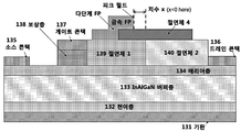
도 3은 본 발명의 제 1 실시예에 따라 형성된 GaN 트랜지스터의 단면도이다. 제 1 절연체(139)는 게이트와 드레인 사이 및 배리어층(134) 위에 배치된다. 제 1 절연체(139)는 높은 게이트-드레인 전하(Qgd)를 야기하는 게이트 근처의 게이트 누설 및 필드를 최소화한다. 인접한 제 2 절연체(140)는 드레인 콘택에서의 전기장을 최소화하고 저저항을 위해 채널에서 높은 전하 밀도를 제공한다. 이 트랜지스터의 나머지 요소/층들은 예를 들어 도 1의 종래 트랜지스터에 도시된 것들일 수 있다. 따라서 본 명세서에서 설명한 다른 부분들에 통합될 수 있다. 이들 요소/층들은 기판(131), 천이층(132), 버퍼층(133), 소스 콘택(135), 드레인 콘택(136), 게이트 콘택(137), 및 보상층(138)을 포함한다.3 is a cross-sectional view of a GaN transistor formed according to a first embodiment of the present invention. The
도 4는 본 발명의 제 2 실시예에 따라 형성된 GaN 트랜지스터의 단면도이다. 도 4는 절연체 1 및 절연체 2의 위치 및 상대적 치수를 나타내는 더 정확한 구조를 도시하고 있다. 도 4는 높은 필드에서 게이트 영역을 보호하는 금속 필드 플레이트를 포함한다. 금속 필드 플레이트는 절연체 2의 일부분 위에만 배치되고, 절연체 1의 전면 위에 배치된다.4 is a cross-sectional view of a GaN transistor formed according to a second embodiment of the present invention. 4 shows a more accurate structure showing the location and relative dimensions of
도 3 및 도 4에 도시된 트랜지스터의 다양한 층 및 이하의 다른 실시예들 및/또는 도면들 중 임의의 도면은 Lidow와 같이 등록된 미국 특허 8350294호의 도 2를 참고하여 형성할 수 있다. 예를 들어, 버퍼, 채널, 배리어, 및 게이트 층은 각각 핵생성(nucleation)에 의해 형성될 수 있다. 일단 게이트 금속이 증착되면 패터닝 및 게이트 물질의 에칭이 수행될 수 있다. 절연체(1)는 배리어에 대한 에칭을 정지시키기 위해 선택적 에칭에 의해 증착되고 패터닝된다. 패시베이션층(108)을 형성하기 위한 도 1 공정 흐름과 비교하여 도 3에서 절연체(139)는 ~100 nm 내지 ~20 nm 범위의 감소된 두께로 형성된다. 그 다음 절연체 2가 증착되고, 패터닝되고, 에칭되어 오믹 개구부를 형성한다. 공정 흐름의 나머지 단계는 전술한 기존 장치의 단계와 유사하거나 동일할 수 있다. 예를 들어, 배리어에 대한 오믹 접촉을 형성하고 필드 플레이트를 형성하기 위해 금속이 증착되고 패터닝되고 에칭될 수 있다.The various layers of the transistors shown in FIGS. 3 and 4 and any of the following other embodiments and/or drawings may be formed with reference to FIG. 2 of U.S. Patent No. 8350294, registered with Lidow. For example, the buffer, channel, barrier, and gate layers may each be formed by nucleation. Once the gate metal is deposited, patterning and etching of the gate material can be performed.
산화물 증착은 라우팅을 위한 추가 금속층에 대해 사용될 수 있다.Oxide deposition can be used for additional metal layers for routing.
절연체 2는 바람직하게 50nm 내지 500nm 범위의 두께로 형성되고, 바람직하게 600°C 내지 900°C의 범위의 고온에서 증착된 SiN으로 만들어진다.
SiN 증착을 위한 전형적인 GaN 처리는 플라즈마 강화 화학 증기 증착(PECVD)에서 300°C 이상에서 한다Typical GaN treatment for SiN deposition is done above 300°C in plasma enhanced chemical vapor deposition (PECVD).
처음 두 실시예(도 3 및 도4)에 있어서, 제 1 절연체 및 제 2 절연체(즉 절연체 1 및 2)는 SiN과 같은 동일한 물질로 형성될 수 있지만, 절연체 1이 절연체 2보다 낮은 도너 상태의 계면 밀도를 생성하도록 상이한 공정 조건을 가질 수 있다. 많은 공정 조건 및 요인(표면 세정, 플라즈마 노출, 예비 증착 표면 준비 및 가스 시퀀싱)은 재료의 공여체 밀도에 영향을 줄 수 있다.In the first two embodiments (FIGS. 3 and 4), the first insulator and the second insulator (i.e. insulators 1 and 2) may be formed of the same material such as SiN, but
바람직한 실시예에서, 본 발명의 트랜지스터의 절연체층은 높은 인터페이스 상태를 위해 저계면 상태에 대해 200mbar 내지 400mbar와 같은 고압 증착 조건, 및 10mbar 내지 100mbar와 같은 저압 증착 조건을 이용하여 형성된다.In a preferred embodiment, the insulator layer of the transistor of the present invention is formed using a high pressure deposition condition such as 200 mbar to 400 mbar for a low interface state, and a low pressure deposition condition such as 10 mbar to 100 mbar for a high interface state.
바람직한 실시예에서, 계면 도핑은 종종 장치를 제조하는 최선의 방법이 아니기 때문에 '계면 밀도가 높은' 영역에서 가장 낮은 계면 밀도가 실제로 사용되고, 절연체 오프셋층이 추가되어 도핑 첨가를 제어할 수 있다.In a preferred embodiment, since interfacial doping is often not the best way to fabricate a device, the lowest interfacial density in the'higher interfacial density' region is actually used and an insulator offset layer can be added to control the doping addition.
본 발명에서, 제 1 절연체 층과 채널 사이의 영역에서의 '순 도핑'은 제 2 절연체층과 채널 사이의 영역에서의 '순 도핑'보다 작으며, 여기서 '순 도핑'은 표면 도너, 배리어층 및 그 영역 내의 임의의 절연체 오프셋층의 의도적인 도핑의 조합이다. 영역의 순 도핑은 계면 상태 밀도를 제어하기 위해 300°C 내지 800°C의 온도에서 1분 내지 10분 동안 NH3에 고온 노출과 같은 표면 사전 침착 작용에 의해 제어될 수 있다. AlGaN 배리어층의 도핑은 700°C 내지 1200°C에서 수행된 배리어층 성장 동안 SiH4 유속을 트리-메틸-갈륨(Tri-Methyl-Gallium) 유속의 1/1000th로 설정하는 것과 같이 증착중 SiH4의 흐름을 통해 달성할 수 있다. 하나 이상의 절연체 오프셋층의 도핑은 절연체 오프셋층 성장 동안 TMG(Tri-Methyl-Gallium)에 대한 SiH4의 유사한 비율의 흐름에 의해 700°C 내지 1200°C에서 이루어질 수 있다.In the present invention, the'pure doping' in the region between the first insulator layer and the channel is less than the'pure doping' in the region between the second insulator layer and the channel, where'net doping' is a surface donor, a barrier layer. And intentional doping of any insulator offset layer within that region. The net doping of the region can be controlled by a surface pre-deposition action such as high temperature exposure to NH3 for 1 to 10 minutes at a temperature of 300°C to 800°C to control the interfacial state density. Doping of the AlGaN barrier layer is performed by setting the SiH4 flow rate to 1/1000 th of the Tri-Methyl-Gallium flow rate during the barrier layer growth performed at 700°C to 1200°C. It can be achieved through flow. Doping of one or more insulator offset layers can be made at 700°C to 1200°C by flow of a similar ratio of SiH4 to Tri-Methyl-Gallium (TMG) during insulator offset layer growth.
도 5a 및 도 5b는 본 발명의 제 2 실시예에 따른 밴드갭에서의 에너지 위치 대 에너지 계면 밀도를 도시하는 배리어층 상의 절연체의 밴드 다이어그램이다. 도 5a를 참조하면, 타입 1의 절연체(즉, 제 1 절연체)는 대부분의 도너가 공백이 되는 상태로 이끄는 전자 도너 밀도가 더 작아짐을 보여준다. 페르미 레벨은 가득찬 상태의 확률이 1/2일 때 도달한다. 도너 상태가 페르미 레벨 이상이 되면, 대부분은 비어 있다. 도 5b를 참조하면, 타입 2의 절연체(즉, 제 2 절연체)는 도너 상태에서 많은 이용 가능한 전자들로 이끄는 도너 밀도가 커짐을 보여준다. 페르미 레벨 아래의 상태들은 주로 전자들로 가득 차 있다. 따라서 상대적인 관점에서 배리어층 위의 순 전자 도너 밀도는 제 2 절연체 아래보다 제 1 절연체 아래에서 낮다.5A and 5B are band diagrams of an insulator on a barrier layer showing energy position versus energy interface density in a bandgap according to a second embodiment of the present invention. Referring to FIG. 5A, it is shown that the
도 6은 본 발명의 제 2 실시예에 따라 형성된 GaN 트랜지스터의 표면 상태에서의 전자량의 묘사를 포함하는 단면도이다. 도 6에 도시된 바와 같이, 버퍼층에 인접한 버퍼층-배리어층의 계면에서 게이트에 더 가까운 표면 상태에서 더 적은 전자가 존재한다.6 is a cross-sectional view including a depiction of the amount of electrons in a surface state of a GaN transistor formed according to a second embodiment of the present invention. As shown in FIG. 6, fewer electrons exist in the surface state closer to the gate at the interface of the buffer layer-barrier layer adjacent to the buffer layer.
도 7은 본 발명의 제 2 실시예에 따라 형성된 GaN 트랜지스터의 단면도로서, 드레인에 전압을 가했을 때의 전자 공핍 폭을 도시한 것이다. 드레인에 전압이 가해지면 표면의 전자와 2DEG가 양의 전압쪽으로 끌어 당겨진다. 전자가 고갈되는 영역은 게이트의 에지에서 시작하여 드레인을 향한 거리, 즉 공핍 폭으로 연장된다. 드레인에서의 전압이 높을수록 고갈 폭은 더 커진다.7 is a cross-sectional view of a GaN transistor formed according to a second embodiment of the present invention, showing an electron depletion width when a voltage is applied to a drain. When a voltage is applied to the drain, electrons and 2DEG on the surface are pulled towards the positive voltage. The region where electrons are depleted starts at the edge of the gate and extends the distance towards the drain, i. The higher the voltage at the drain, the greater the depletion width.
도 8은 본 발명의 제 2 실시예에 따라 형성된 GaN 트랜지스터의 공핍 길이 vs 드레인 인가 전압을 나타낸 것이다. 낮은 바이어스 영역, 즉 절연체 1의 영역은 공핍 길이가 보다 빠르게 상승한다. 이것은 Qdg가 더 낮고 게이트로 충전되는 전하가 적기 때문에(도 1의 장치와 같은) 단일 절연체 프로세스보다 우수하다. 높은 바이어스 영역, 즉 절연체 2의 영역에서 공핍은 상승하기에 매우 느리다. 이것은 소자가 시간이 지남에 따라 저항에 변화가 오기 전에 드레인 에지에만 갈 수 있기에 유용하다. 두개의 절연체 프로세스가 있으면 저항이 변경되기 전에 더 높은 전압을 허용할 수 있다.8 shows a depletion length vs. drain applied voltage of a GaN transistor formed according to a second embodiment of the present invention. In the low bias region, that is, the region of
도 9는 본 발명의 제 2 실시예에 따라 형성된 GaN 트랜지스터의 전자기장 vs 드레인까지의 거리를 나타낸 것이다. 도 9에 도시된 바와 같이, 드레인 인근에서 특정 전압이 인가된 후 필드가 크게 증가하기 시작한다. 이 전압은 필드가 빠르게 상승하기 시작할 때 공핍 폭이 드레인 접점에 도달하면 발생한다.9 shows the electromagnetic field vs. the distance to the drain of the GaN transistor formed according to the second embodiment of the present invention. As shown in FIG. 9, after a specific voltage is applied near the drain, the field starts to increase significantly. This voltage occurs when the depletion width reaches the drain contact when the field starts to rise rapidly.
따라서, 제 1 및 제 2 실시예에서의 2단계 절연체의 이점은 시간에 따른 저항 변화없이 더 낮은 Qdg를 가질 수 있고 더 높은 전압 동작을 갖는 것이다.Thus, the advantage of the two-stage insulator in the first and second embodiments is that it can have a lower Q dg and have a higher voltage operation without changing the resistance over time.
도 10은 본 발명의 제 2 실시예에 따른 밴드갭 내의 고온 전자의 인접한 트랩 상태로의 산란을 도시하는 배리어층 상의 절연체의 밴드 다이어그램이다. Rdson 변경 전의 전압 제한은 높은 전계와 '핫 일렉트론'에 의해 발생한다. 누설 전류가 발생하면 전자는 게이트/소스 측에서 드레인측으로 배리어층 바로 아래 영역으로 이동한다. 전계가 높은 영역에서는 전자가 더 빨리 이동한다. 필드가 매우 높으면 전자는 많은 에너지를 얻을 수 있다. 그들이 무언가를 치고 흩어지면 채널 밖으로 흘러 배리어 안의 장소, 경계면 또는 배리어 위의 절연체로 흩어질 수 있다. 사용할 수 있는 상태가 있으면 해당 상태로 들어갈 수 있다. 이러한 상태는 전자를 포착하기 때문에 트랩 상태라고 한다. Fig. 10 is a band diagram of an insulator on a barrier layer showing scattering of hot electrons in a band gap into an adjacent trap state according to a second embodiment of the present invention. The voltage limit before the Rdson change is caused by high electric fields and'hot electrons'. When a leakage current occurs, electrons move from the gate/source side to the drain side and to the region just below the barrier layer. In the high electric field, electrons move faster. If the field is very high, electrons can get a lot of energy. When they hit something and disperse, they can flow out of the channel and scatter into places within the barrier, at boundaries, or into insulators above the barrier. If there is a state available, you can enter that state. This state is called a trap state because it captures electrons.
도 11은 본 발명의 제 3 실시예에 따라 형성된 GaN 트랜지스터의 단면도이다. 도 11에 도시된 바와 같이, 절연체 오프셋층은 제 2 절연체와 배리어층(134) 사이에 위치한다.11 is a cross-sectional view of a GaN transistor formed according to a third embodiment of the present invention. As shown in FIG. 11, the insulator offset layer is positioned between the second insulator and the barrier layer 134.
도 12는 본 발명의 제 3 실시예에 따른 밴드갭에서 중간 반도체 오프셋층을 사용하면서 배리어층에 걸친 절연체의 밴드 다이어그램이다. 제 3 실시예는 배리어와 제 2 절연체 사이의 반도체 오프셋층에 의해 SiN과 같은 트랩-함유 절연체를 채널로부터 더 멀리 이동시키는 것에 기초한다. 하나의 층에 대해 넓은 밴드갭 재료로 만들어줌으로써 핫 일렉트론이 극복할 수 있는 더 높은 배리어가 만들어진다.12 is a band diagram of an insulator over a barrier layer while using an intermediate semiconductor offset layer in a band gap according to a third embodiment of the present invention. The third embodiment is based on moving a trap-containing insulator such as SiN further away from the channel by means of a semiconductor offset layer between the barrier and the second insulator. By making a wide bandgap material for one layer, a higher barrier is created that hot electrons can overcome.
도 13a 내지 도 13g는 본 발명의 제 2 실시예에 따른 GaN 트랜지스터를 제조하기 위한 공정 흐름도이다.13A to 13G are process flow diagrams for manufacturing a GaN transistor according to a second embodiment of the present invention.
도 14는 본 발명의 제 3 실시예에 따른 GaN 트랜지스터의 형성을 도시한 것이다. 제 3 실시예의 디바이스 형성 프로세스는 (절연체) 오프셋층이 절연체 2 전에 증착되는 것을 제외하고는 도 13a 내지 도 13g에 도시된 것과 동일하다. 오프셋층은 선택적으로 도너 원자로 도핑될 수 있다.14 shows the formation of a GaN transistor according to a third embodiment of the present invention. The device formation process of the third embodiment is the same as that shown in Figs. 13A to 13G except that the (insulator) offset layer is deposited before the
도 15a 및 도 15b는 본 발명의 제 3 실시예에 따른 밴드갭에서의 중간 반도체 오프셋층의 도핑 동기를 나타낸 밴드 다이어그램이다. 도 15a에 도시된 바와 같이, 드레인 에지에서 전기장을 감소시키는데 사용되는 계면 상태는 활성화 에너지라 지칭되는 방출에 대한 다소 큰 에너지 배리어를 갖는다. 활성화 에너지로 인해 전기장에 반응하는데 일정한 시간이 걸린다. 더 큰 활성화 에너지는 더 긴 방출 시간과 같다. 스위칭 애플리케이션에서 시간은 인터페이스 전자가 응답하는데 필요한 시간보다 훨씬 더 짧아질 수 있다. 도 15b에 도시된 바와 같이, 보다 낮은 계면 상태와 절연체 오프셋층의 도핑을 조합함으로써, 장치는 GaN에서 Si에 대해 10mV와 같은 매우 낮은 활성화 에너지를 가질 수 있다. 이것은 응답 시간을 대폭적으로 향상시킨다. 또한 이전에 계면에 있던 전자는 2DEG에 전자를 제공하는 도너로 대체된다. 따라서 장치의 전도도가 높아져 성능이 향상된다. 본 발명의 바람직한 실시예에서, 제 2 절연체 아래의 2DEG 시트 저항은 450Ω/sq(또는 350-600 Ω/sq)이고, 제 1 절연체 아래의 2DEG 시트 저항은 800 Ω/sq(또는 600-1000 Ω/sq)이다.15A and 15B are band diagrams showing doping synchronization of an intermediate semiconductor offset layer in a band gap according to a third embodiment of the present invention. As shown in FIG. 15A, the interfacial state used to reduce the electric field at the drain edge has a rather large energy barrier to emission, referred to as activation energy. Due to the activation energy, it takes a certain amount of time to react to the electric field. A greater activation energy is equal to a longer release time. In switching applications, the time can be much shorter than the time required for the interface electronics to respond. As shown in Fig. 15B, by combining the lower interfacial state with the doping of the insulator offset layer, the device can have a very low activation energy, such as 10 mV for Si in GaN. This significantly improves the response time. Also, electrons that were previously at the interface are replaced by donors that donate electrons to the 2DEG. Therefore, the conductivity of the device is increased and the performance is improved. In a preferred embodiment of the invention, the 2DEG sheet resistance under the second insulator is 450Ω/sq (or 350-600 Ω/sq), and the 2DEG sheet resistance under the first insulator is 800 Ω/sq (or 600-1000 Ω). /sq).
도 16은 본 발명의 제 4 실시예에 따라 형성된 GaN 트랜지스터의 단면도이다. 이 실시예는 제 3 실시예와 유사하지만, 게이트 영역에 걸친 절연체 오프셋층의 제거의 차이점이 있다. 이것은 선택적 증착 또는 마스크 및 에칭에 의해 수행될 수 있다. GaN 성장에서 실제로 SiN 및 SiO2와 같은 절연체의 성장을 강제하기 어렵기에, 게이트 위에 절연체 오프셋 영역이 없더록 선택 증착하기는 쉽다.16 is a cross-sectional view of a GaN transistor formed according to a fourth embodiment of the present invention. This embodiment is similar to the third embodiment, but differs in the removal of the insulator offset layer over the gate region. This can be done by selective deposition or masking and etching. Since it is difficult to actually force the growth of insulators such as SiN and SiO2 in GaN growth, it is easy to selectively deposit without an insulator offset region on the gate.
도 17은 본 발명의 제 5 실시예에 따라 형성된 GaN 트랜지스터의 단면도이다. 이는 절연체 1의 일부가 드레인 영역 근처에 남아 있다는 점을 제외하고는 제 4 실시예와 유사하다. 이는 오프셋 스페이서층을 통해 2DEG 영역에 오믹 접촉을 하는 것이 어려울 수 있기에 공정상 유리하다.17 is a cross-sectional view of a GaN transistor formed according to a fifth embodiment of the present invention. This is similar to the fourth embodiment except that part of the
도 18은 본 발명의 제 6 실시예에 따라 형성된 GaN 트랜지스터의 단면도이다. 제 6 실시예는 게이트의 에지 부근에 제 3 절연 물질을 포함한다. 이는 자기 정렬식 에치백을 이용하여 만들 수 있다. 이 공정은 측면 벽을 코팅하는 얇은 층을 증착한 후 마스킹하지 않고 직접 에칭한다. 목표는 게이트 누설을 줄이고 Qgd를 더욱 줄이기 위해 게이트 측면을 따라 더 낮은 인터페이스 밀도를 갖는 것이다. 이는 마스크 기반 프로세스를 사용하여 생성할 수 있다. 목표는 게이트 근처 및 영역의 가장 높은쪽/중간/드레인쪽에서 가장 낮은 밀도를 갖는 것이다.18 is a cross-sectional view of a GaN transistor formed according to a sixth embodiment of the present invention. The sixth embodiment includes a third insulating material near the edge of the gate. This can be made using a self-aligned etchback. This process deposits a thin layer that coats the side walls and then directly etchs without masking. The goal is to have a lower interface density along the gate side to reduce gate leakage and further reduce Q gd . This can be created using a mask-based process. The goal is to have the lowest density near the gate and at the highest/middle/drain side of the area.
도 19는 본 발명의 실시예들 중 어느 하나에 따른 GaN 트랜지스터에 대해, 소자를 파괴하지 않고 저항 변화를 일으키지 않고 전류가 반복적으로 상승하는 500V 브레이크다운 중 200V 부분을 도시한 것이다. 이는 본 발명의 2단계 절연체 공정이 어떻게 안정한 브레이크다운을 일으키는지 보여준다. 그 결과 안정적인 내성을 가진 브레이크다운용 부품의 성능이 두배가 되며, 안정적인 고장 메커니즘을 가질 수 있다. 이를 통해 장치는 과전압을 견딜 수 있고, 모터 드라이브와 같이 부하 유도성이 강한 애플리케이션에서 유용하다. 일반적으로 이 유형의 펄스 이후 트랜지스터는 단선되거나 단락된다.FIG. 19 is a diagram illustrating a 200V portion of a 500V breakdown in which a current repeatedly increases without destroying an element and without causing a resistance change in the GaN transistor according to any one of the embodiments of the present invention. This shows how the two stage insulator process of the present invention produces a stable breakdown. As a result, the performance of the breakdown component with stable tolerance is doubled and a stable failure mechanism can be obtained. This allows the device to withstand overvoltage and is useful in applications with strong load induction, such as motor drives. Usually, the transistor is shorted or shorted after this type of pulse.
도 20은 본 발명의 제 7 실시예에 따라 형성된 GaN 트랜지스터의 단면도이다. 이는 제 3 실시예에 기초한다. 절연체 오프셋층은 소스 및/또는 드레인 콘택 아래에 있고, 이는 드레인/소스 채널에서 오믹 접촉 저항을 감소시킬 수 있다.20 is a cross-sectional view of a GaN transistor formed according to a seventh embodiment of the present invention. This is based on the third embodiment. An insulator offset layer is below the source and/or drain contacts, which can reduce the ohmic contact resistance in the drain/source channels.
도 21은 본 발명의 제 8 실시예에 따라 형성된 GaN 트랜지스터의 단면도이다.21 is a cross-sectional view of a GaN transistor formed according to an eighth embodiment of the present invention.
이 실시예에서, 금속 필드판은 절연체 1 위에 포함된다. 절연체 1/절연체 2 경계에 대한 금속 필드 판의 상대적 위치는 치수 x로 도시된다. X의 크기는 -1um에서 +0.5um까지이다. 음의 x는 금속 필드 플레이트가 경계로부터 x만큼 멀어지며 절연체 2와 겹치지 않음을 의미한다. 양의 x는 금속 필드 플레이트가 절연체 2 위에 있고 x의 길이만큼 덮는 것을 의미한다.In this embodiment, a metal field plate is included over the
도 22는 본 발명의 제 8 실시예에 따라 형성된 GaN 트랜지스터의 표면 상태에서의 전자량을 도시한 단면도이다. 도 22에 도시된 바와 같이, x는 -0.5um과 같이 금속 필드 플레이트 팁에서 낮은 필드의 음수 값이 좋다. 절연체 1 아래의 표면 상태에서 절연체 2보다 전자가 적기 때문에, 절연체 1 아래의 공핍은 오프 상태에서 더 빠르다. 따라서 금속 필드 플레이트의 팁에서의 피크 필드는 음의 x로 낮아진다.22 is a cross-sectional view showing the amount of electrons in a surface state of a GaN transistor formed according to an eighth embodiment of the present invention. As shown in FIG. 22, x is a negative value of a low field in the metal field plate tip, such as -0.5um. Since there are fewer electrons in the surface state under
도 23은 본 발명의 제 8 실시예에 따라 형성된 GaN 트랜지스터의 금속 필드 플레이트 횡 방향 길이에 대한 전자기장을 도시한 것이다. 도 23에 도시된 바와 같이, x<0은 x>0보다 금속 필드 플레이트 에지에서 더 낮은 피크 필드를 갖는다. 따라서 x<0인 설계는 오프 상태에서 더욱 안정한 브레이크다운 전압을 특징으로 한다.23 illustrates an electromagnetic field with respect to a length in a transverse direction of a metal field plate of a GaN transistor formed according to an eighth embodiment of the present invention. As shown in Fig. 23, x<0 has a lower peak field at the metal field plate edge than x>0. Therefore, designs with x<0 feature a more stable breakdown voltage in the off state.
도 24은 본 발명의 제 9 실시예에 따라 형성된 GaN 트랜지스터의 단면도이다. 제 9 실시예는 제 8 실시예에 기초한다. 장치 제조시 절연체 1 위에 절연체 2를 갖는 것이 더 실용적이다. x의 크기는 일반적으로 -1um~ +0.5um이다. 음의 x는 금속 필드 플레이트가 x만큼 경계로부터 멀어지며 절연체 2와 겹치지 않음을 의미한다. 양의 x는 금속 필드 플레이트가 절연체 2 위에 있고 x의 길이만큼 덮는 것을 의미한다.24 is a cross-sectional view of a GaN transistor formed according to a ninth embodiment of the present invention. The ninth embodiment is based on the eighth embodiment. It is more practical to have
도 25은 본 발명의 제 10 실시예에 따라 형성된 GaN 트랜지스터의 단면도이다. 제 10 실시예는 제 9 실시예에 기초한다. 금속 필드 플레이트 아래의 절연체 2 및 절연체 1은 부분적으로 식각되어 다양한 높이의 다중 단계 금속 필드 플레이트를 형성한다. 다단계 금속 필드 플레이트를 갖는 설계는 금속 필드 플레이트 팁에서의 피크 필드를 드레인쪽으로 더욱 감소시킨다. x의 크기는 -1um ~ +0.5um이다.25 is a cross-sectional view of a GaN transistor formed according to a tenth embodiment of the present invention. The tenth embodiment is based on the ninth embodiment.
도 26은 본 발명의 제 11 실시예에 따라 형성된 GaN 트랜지스터의 단면도이다. 절연체 4는 절연체 1 및/또는 절연체 2 위에 위치하며, 이는 다중 단계 금속 필드 플레이트를 형성한다. 다단계 금속 필드 플레이트를 갖는 설계는 금속 필드 플레이트 팁에서의 피크 필드를 드레인쪽으로 더욱 감소시킨다. x의 크기는 -1um ~ +0.5um이다. 음의 x는 금속 필드 플레이트가 x만큼 경계로부터 멀어지며 절연체 2와 겹치지 않음을 의미한다. 양의 x는 금속 필드 플레이트가 절연체 2 위에 있고 x의 길이만큼 덮는 것을 의미한다.26 is a cross-sectional view of a GaN transistor formed according to an eleventh embodiment of the present invention. Insulator 4 is placed over
도 27 내지 도 31은 이전에 기술된 실시예의 추가적인 변형 및 세부 사항을 도시한다. 도 27은 제 2 절연체(ILD2)와 드레인(D) 사이의 부가적인 제 3 절연체(ILD3) 및 제 4 절연체(ILD4)를 갖는 트랜지스터를 도시한다. ILD2, ILD3, ILD4,... 는 절연체 오프셋층 및 절연체 오프셋층이 배리어 높이를 향상시키고 2DEG 밀도를 증가시킬 수 있는 절연막을 포함할 수 있다.27-31 show additional variations and details of the previously described embodiment. FIG. 27 shows a transistor having an additional third insulator ILD3 and a fourth insulator ILD4 between the second insulator ILD2 and the drain D. ILD2, ILD3, ILD4,... may include an insulator offset layer and an insulating layer in which the insulator offset layer can improve the barrier height and increase the 2DEG density.
도 28은 ILD1, ILD2, ILD3까지 2DEG 밀도가 증가하는 것을 도시한다.Figure 28 shows the increase in 2DEG density up to ILD1, ILD2, and ILD3.
도 29는 전술한 금속 필드 스페이싱을 갖는 실시예를 도시한다. 도 30은 ILD1, ILD2, ILD3,...등을 형성함으로써 이전에 기술된 게단 금속 필드 플레이팅을 도시한다. 도 31은 EPI 층과 접촉하지 않는 ILDx에 의한 계단식(다단계) 금속 필드 플레이팅을 도시한다.29 shows an embodiment with the metal field spacing described above. 30 shows the metal field plating previously described by forming ILD1, ILD2, ILD3,...etc. 31 shows stepwise (multi-step) metal field plating with ILDx not in contact with the EPI layer.
도 32는 본 발명의 제 2 실시예에 따라 형성된 GaN 트랜지스터의 단면도이다. 이 실시예의 트랜지스터는 다음의 구성 요소를 포함한다. 101은 기판, 102는 천이층, 103은 도핑되지 않은 GaN 버퍼층이며 전형적으로 0.5um 내지 10um의 두께를 갖고, 104는 도핑되지 않은 AlGaN 배리어층으로 전형적으로 50A 내지 300A 두께이고, Al%는 12% 내지 28%이며, 105는 보상 반도체층, 139는 절연체 1, 140은 절연체 2, 201은 소스 콘택, 202는 게이트 콘택, 203은 드레인 콘택, 301은 배리어(104) 위의 금속으로 금속 필드 플레이트, 302는 배리어와 절연체 2 계면 위에 있는 금속(301)의 드레인측 에지이다. 여기서 소스(201)와 금속(301)은 이 구조로 연결되거나 또는 분리될 수 있다. 공정 순서는 절연체 1 다음 절연체 2의 순서이다(절연체 1이 먼저 형성되고 절연체 2 형성).32 is a cross-sectional view of a GaN transistor formed according to a second embodiment of the present invention. The transistor of this embodiment includes the following components. 101 is a substrate, 102 is a transition layer, 103 is an undoped GaN buffer layer and typically has a thickness of 0.5 μm to 10 μm, 104 is an undoped AlGaN barrier layer, typically 50 A to 300 A thickness, and Al% is 12% To 28%, 105 is a compensation semiconductor layer, 139 is an
도 33은 전술한 제 2 실시예에 따라 형성되지만 측방향으로 단축된 필드 플레이트를 갖는 GaN 트랜지스터의 단면도를 도시한다. 도 32의 제 2 실시예와 비교하여, 302에서의 피크 필드는 배리어와 절연체 1의 계면에서의 고갈에 의해 감소되어 넓은 공핍 폭을 생성한다.Fig. 33 shows a cross-sectional view of a GaN transistor formed according to the second embodiment described above but having a field plate shortened laterally. Compared with the second embodiment of Fig. 32, the peak field at 302 is reduced by depletion at the interface of the barrier and
도 34는 전술한 제 2 실시예에 따라 형성된 GaN 트랜지스터의 단면도를 도시하지만, 제 2 절연체(140)는 게이트 위에 횡방향으로 연장되지 않으므로, 도 32 및 도 33과 비교하여, 제 1 절연체(139)만이 금속(301)과 배리어층(104) 사이에 존재하며 결과적으로 유전체층이 더 얇아지고 필드 플레이팅 효과가 우수해진다.34 is a cross-sectional view of the GaN transistor formed according to the second embodiment described above, but since the
도 35는 도 34와 유사한 GaN 트랜지스터의 단면도를 도시한다. 하지만 필드 플레이트 금속(301)은 제 2 절연체(140) 위에 측방향으로 연장된다. 도 34와 같이, 제 1 절연체(139)만이 금속(301)과 배리어층(104) 사이에 있으며, 결과적으로 유전체층이 더 얇아지고 필드 플레이팅 효과가 우수해진다.FIG. 35 shows a cross-sectional view of a GaN transistor similar to that of FIG. 34. However, the
도 36은 전술한 실시예들과 유사한 GaN 트랜지스터의 단면도를 도시하지만, 게이트 근처에서 제 2 절연체(140)를 에칭 제거함으로써 더 나은 필드 플레이팅 효과를 가질 수 있다.FIG. 36 shows a cross-sectional view of a GaN transistor similar to the above-described embodiments, but it is possible to have a better field plating effect by etching away the
도 37은 도 36과 유사한 GaN 트랜지스터의 단면도를 도시한다. 소스(201)과 금속(301)은 이 구조로 연결되지만 선택적으로 분리될 수도 있다.37 is a cross-sectional view of a GaN transistor similar to that of FIG. 36. The
도 38은 도 34와 유사한 GaN 트랜지스터의 단면도를 도시한다. 이는 게이트 근처에서 절연체 2를 에칭 제거함으로써 더 나은 필드 플레이팅 효과를 갖는다.38 shows a cross-sectional view of a GaN transistor similar to that of FIG. 34. This has a better field plating effect by etching away
도 39는 전술한 실시예들과 유사한 GaN 트랜지스터의 단면도를 도시하지만, 게이트(202)와 드레인(203) 사이의 보다 균일한 측방 필드 분포를 얻기 위해 다수의 필드 플레이팅(및 제 3 절연체(141))을 갖는다.39 shows a cross-sectional view of a GaN transistor similar to the above-described embodiments, but multiple field plating (and third insulator 141) to obtain a more uniform lateral field distribution between the
도 40은 도 39와 유사한 다중 필드 플레이트를 갖는 GaN 트랜지스터의 단면도를 도시한다. 하지만 필드 플레이트(301)는 제 3 절연체(141) 위에 측방향으로 연장된다.40 shows a cross-sectional view of a GaN transistor having a multi-field plate similar to that of FIG. 39; However, the
도 41은 도 39와 유사한 GaN 트랜지스터의 단면도를 도시한다. 게이트(202)와 드레인(203) 사이의 보다 균일한 측방 필드 분포를 얻기 위해 다수의 필드 플레이팅을 갖지만, 필드 플레이팅 효과를 향상시키기 위해 게이트 부근에서 절연체 2가 에칭 제거된다.41 shows a cross-sectional view of a GaN transistor similar to that of FIG. 39. It has a large number of field plating to obtain a more uniform lateral field distribution between the
도 42는 도 40과 유사한 GaN 트랜지스터의 단면도를 도시한다. 게이트(202)와 드레인(203) 사이의 보다 균일한 측방 필드 분포를 얻기 위해 다수의 필드 플레이팅을 갖지만, 필드 플레이팅 효과를 향상시키기 위해 게이트 부근에서 절연체 2가 에칭 제거된다.42 shows a cross-sectional view of a GaN transistor similar to that of FIG. 40. It has a large number of field plating to obtain a more uniform lateral field distribution between the
도 43은 도 42와 유사한 GaN 트랜지스터의 단면도를 도시한다. 게이트(202)와 드레인(203) 사이의 보다 균일한 측방 필드 분포를 얻기 위해 다수의 필드 플레이팅을 갖지만, 도 40에 도시된 바와 같이 필드 플레이트(301)는 제 3 절연체(141) 위에 측방향으로 연장된다.43 shows a cross-sectional view of a GaN transistor similar to that of FIG. 42. In order to obtain a more uniform lateral field distribution between the
도 44는 도 42와 유사한 GaN 트랜지스터의 단면도를 도시한다. 게이트의 소스측이 아니라 드레인측 상에 계단형 필드 플레이트가 구비된다.44 shows a cross-sectional view of a GaN transistor similar to that of FIG. 42. A stepped field plate is provided on the drain side rather than the source side of the gate.
도 45는 도 32의 GaN 트랜지스터를 제조하기 위한 예시적인 프로세스 흐름을 도시한다.45 shows an exemplary process flow for fabricating the GaN transistor of FIG. 32;
도 46는 도 35의 GaN 트랜지스터를 제조하기 위한 예시적인 프로세스 흐름을 도시한다.46 shows an exemplary process flow for fabricating the GaN transistor of FIG. 35;
도 47는 도 37의 GaN 트랜지스터를 제조하기 위한 예시적인 프로세스 흐름을 도시한다.47 shows an exemplary process flow for fabricating the GaN transistor of FIG. 37;
도 48는 도 40의 GaN 트랜지스터를 제조하기 위한 예시적인 프로세스 흐름을 도시한다.48 shows an exemplary process flow for fabricating the GaN transistor of FIG. 40.
도 49는 도 42의 GaN 트랜지스터를 제조하기 위한 예시적인 프로세스 흐름을 도시한다.49 shows an exemplary process flow for fabricating the GaN transistor of FIG. 42;
도 50는 도 44의 GaN 트랜지스터를 제조하기 위한 예시적인 프로세스 흐름을 도시한다.50 shows an exemplary process flow for fabricating the GaN transistor of FIG. 44;
여기에 기술된 임의의 실시예의 방법 단계는 임의의 특정 순서로 수행되는 것으로 제한되지 않는다. 또한 임의의 방법 실시예들에서 언급된 구조들은 임의의 장치 실시예들에서 언급된 구조들을 이용할 수 있다. 이러한 구조는 장치 실시예에 대해서만 상세히 설명될 수 있지만, 방법 실시예 중 임의의 것에 적용 가능하다.The method steps of any of the embodiments described herein are not limited to being performed in any particular order. Also, structures mentioned in certain method embodiments may use structures mentioned in certain device embodiments. This structure may be described in detail only for device embodiments, but is applicable to any of the method embodiments.
여기서 설명된 임의의 실시예의 특징은 본 명세서에 기술된 다른 실시예에서의 특징과 조합하여 사용될 수 있고, 이러한 조합은 본 발명의 사상 및 범위 내에 있는 것으로 간주된다.Features of any of the embodiments described herein may be used in combination with features of other embodiments described herein, and such combinations are considered to be within the spirit and scope of the present invention.
본 발명에서 구체적으로 언급되고 고려된 수정 및 변형은 본 발명의 사상 및 범위 내에 있는 것으로 간주된다.Modifications and modifications specifically mentioned and contemplated in the present invention are considered to be within the spirit and scope of the present invention.
전술한 설명 및 도면들은 여기에 설명된 특징 및 이점을 달성하는 특정 실시예를 예시하는 것으로 간주된다. 특정 공정 조건에 대한 변경 및 대체가 이루어질 수 있다. 따라서 본 발명의 실시예는 전술한 설명 및 도면에 의해 제한되는 것으로 간주되지 않는다.The foregoing description and drawings are considered to illustrate specific embodiments that achieve the features and advantages described herein. Changes and substitutions for specific process conditions can be made. Accordingly, embodiments of the present invention are not considered to be limited by the foregoing description and drawings.
보다 일반적으로, 본 발명은 예시적인 실시예가 첨부된 도면에 따른 예를 참조하여 상술되었지만, 이들로 제한되지 않는 것으로 이해되어야 한다. 오히려 개시된 실시예가 본 발명의 개시 내용의 범위를 벗어나지 않으면서 다양한 방식으로 변형될 수 있음은 당업자에게 명백하다. 또한, 본 명세서에 사용된 용어 및 설명은 단지 설명을 위한 것이며 한정적인 의미인 것은 아니다. 당업자는 달리 언급되지 않는한 모든 용어를 가능한 가장 넓은 의미로 이해하여야 한다. 이하의 청구항 및 그의 균등물에 정의된 바와 같은 본 발명의 사상 및 범위 내에서 많은 변형이 가능하다는 것을 인식해야 한다.More generally, although the present invention has been described above with reference to examples according to the accompanying drawings, it is to be understood that exemplary embodiments are not limited thereto. Rather, it is apparent to those skilled in the art that the disclosed embodiments may be modified in various ways without departing from the scope of the present disclosure. In addition, terms and descriptions used herein are for illustrative purposes only and are not intended to be limiting. Those skilled in the art should understand all terms in the broadest possible meaning, unless stated otherwise. It should be appreciated that many modifications are possible within the spirit and scope of the invention as defined in the following claims and their equivalents.
Claims (15)
상기 기판 상부에 배치되고, III족 질화물 물질을 포함하는 천이층;
상기 천이층 상부에 배치되고, III족 질화물 물질을 포함하는 버퍼층;
상기 버퍼층 바로 상부에 배치되고, III족 질화물 물질을 포함하는 배리어층;
상기 버퍼층 내에서 상기 배리어층과 접합하는 부분에 형성된 전도성 2차원 전자 가스(2DEG)를 포함하는 채널;
상기 배리어층 상부에 배치되는 게이트 콘택, 드레인 콘택, 및 소스 콘택; 및
상기 배리어층 상부에 배치되고, 적어도 게이트 콘택과 드레인 콘택 사이에 배치되는 제 1 절연체 및 제 2 절연체를 포함하고,
상기 게이트 콘택은 상기 소스 콘택 및 상기 드레인 콘택 사이에 배치되고,
상기 제 1 절연체는 상기 제 2 절연체보다 상기 게이트 콘택에 더 가까이 배치되고,
상기 제 2 절연체 하부 채널 내의 2DEG 밀도가 상기 제 1 절연체 하부 채널 내의 2DEG 밀도보다 높도록, 상기 제 1 절연체 하부 채널 위의 순 전자 도너 밀도는 상기 제 2 절연체 하부 채널 위의 순 전자 도너 밀도보다 낮은, III족 질화물 트랜지스터.
Board;
A transition layer disposed on the substrate and including a group III nitride material;
A buffer layer disposed on the transition layer and including a group III nitride material;
A barrier layer disposed immediately above the buffer layer and including a group III nitride material;
A channel including a conductive two-dimensional electron gas (2DEG) formed in a portion of the buffer layer that is bonded to the barrier layer;
A gate contact, a drain contact, and a source contact disposed on the barrier layer; And
A first insulator and a second insulator disposed on the barrier layer and disposed between at least the gate contact and the drain contact,
The gate contact is disposed between the source contact and the drain contact,
The first insulator is disposed closer to the gate contact than the second insulator,
The net electron donor density on the first insulator lower channel is lower than the net electron donor density on the second insulator lower channel so that the 2DEG density in the second insulator lower channel is higher than the 2DEG density in the first insulator lower channel. , Group III nitride transistor.
상기 제 1 절연체는 상기 제 2 절연체보다 표면 상태에서 더 적은 전자를 갖는, III족 질화물 트랜지스터.
The method of claim 1,
The first insulator has fewer electrons in a surface state than the second insulator.
상기 버퍼층 또는 상기 배리어층에 포함되는 III족 질화물 물질은 GaN 물질을 포함하는, III족 질화물 트랜지스터.
The method of claim 1,
The group III nitride material included in the buffer layer or the barrier layer includes a GaN material.
적어도 상기 제 2 절연체 및 상기 배리어층 사이에 배치되는 절연체 오프셋층을 더 포함하는, III족 질화물 트랜지스터.
The method of claim 1,
A group III nitride transistor, further comprising an insulator offset layer disposed between at least the second insulator and the barrier layer.
상기 절연체 오프셋층은 III족 질화물 물질을 포함하는, III족 질화물 트랜지스터.
The method of claim 4,
The insulator offset layer comprises a group III nitride material.
상기 절연체 오프셋층에 포함되는 III족 질화물 물질은 AlN, AlGaN 및 GaN 물질 중 하나 이상을 포함하는, III족 질화물 트랜지스터.
The method of claim 5,
The group III nitride material included in the insulator offset layer includes at least one of AlN, AlGaN, and GaN materials.
상기 절연체 오프셋층에 포함되는 III족 질화물 물질은 도핑되어 있는 , III족 질화물 트랜지스터.
The method of claim 6,
The group III nitride material included in the insulator offset layer is doped.
상기 드레인 콘택은 상기 절연체 오프셋층의 제거된 부분을 통해 상기 배리어층과 접촉하는, III족 질화물 트랜지스터.
The method of claim 4,
The drain contact is in contact with the barrier layer through the removed portion of the insulator offset layer.
상기 절연체 오프셋층은 상기 드레인 콘택과 상기 배리어층 사이에 배치되는, III족 질화물 트랜지스터.
The method of claim 4,
The insulator offset layer is disposed between the drain contact and the barrier layer.
금속 필드 플레이트를 더 포함하고,
상기 금속 필드 플레이트는,
상기 제 1 절연체 및 상기 제 2 절연체 중 적어도 하나의 상부;
제 2 절연체의 상부가 아니고, 적어도 상기 게이트 콘택과 드레인 콘택 사이이고, 제 1 절연체의 상부;
적어도 상기 게이트 콘택과 드레인 콘택 사이이고, 상기 제 1 절연체와 상기 제 2 절연체의 상부; 또는
적어도 상기 게이트 콘택과 드레인 콘택 사이이고, 상기 제 1 절연체와 상기 제 2 절연체 중 적어도 하나의 상부에 배치되고,
상기 게이트 콘택과 드레인 콘택 사이에 배치된 상기 금속 필드 플레이트는 다양한 높이를 갖는 다수의 스텝을 포함하는, III족 질화물 트랜지스터.
The method of claim 1,
Further comprising a metal field plate,
The metal field plate,
An upper portion of at least one of the first insulator and the second insulator;
An upper portion of the first insulator that is not above the second insulator, but is at least between the gate contact and the drain contact;
At least between the gate contact and the drain contact, the upper portion of the first insulator and the second insulator; or
At least between the gate contact and the drain contact, and disposed on at least one of the first insulator and the second insulator,
The metal field plate disposed between the gate contact and the drain contact includes a plurality of steps having various heights.
상기 제 2 절연체는 상기 제 1 절연체의 전면의 상부 또는 상기 제 1 절연체의 일부분의 상부에 배치되는, III족 질화물 트랜지스터.
The method of claim 1,
The second insulator is disposed on a front surface of the first insulator or on a portion of the first insulator.
상기 제 1 절연체는 상기 제 2 절연체의 전면의 상부 또는 상기 제 2 절연체의 일부분의 상부에 배치되는, III족 질화물 트랜지스터.
The method of claim 1,
The first insulator is disposed on a front surface of the second insulator or on a portion of the second insulator.
적어도 상기 게이트 콘택과 드레인 콘택 사이이고, 상기 제 2 절연체 및 제 1 절연체의 상부에 배치되는 제 3 절연체를 더 포함하는, III족 질화물 트랜지스터.
The method of claim 1,
A group III nitride transistor, further comprising a third insulator disposed at least between the gate contact and the drain contact and disposed above the second insulator and the first insulator.
금속 필드 플레이트를 더 포함하고,
상기 금속 필드 플레이트는,
상기 제 2 절연체의 상부가 아니고, 적어도 상기 게이트 콘택과 드레인 콘택 사이이고, 상기 제 1 절연체 및 상기 제 3 절연체의 상부; 또는
적어도 상기 게이트 콘택과 드레인 콘택 사이이고, 상기 제 1 절연체, 상기 제 2 절연체, 및 상기 제 3 절연체의 상부에 배치되는, III족 질화물 트랜지스터.
The method of claim 13,
Further comprising a metal field plate,
The metal field plate,
Not an upper portion of the second insulator, at least between the gate contact and the drain contact, and an upper portion of the first insulator and the third insulator; or
A group-III nitride transistor, at least between the gate contact and the drain contact, and disposed above the first insulator, the second insulator, and the third insulator.
상기 배리어층은 InxAlyGa(1-x-y)N을 포함하고, 여기서 x+y ≤ 1 인, III족 질화물 트랜지스터.The method of claim 2,
The barrier layer includes In x Al y Ga (1-xy) N, wherein x+y ≤ 1, a group III nitride transistor.
Applications Claiming Priority (5)
| Application Number | Priority Date | Filing Date | Title |
|---|---|---|---|
| US201662344151P | 2016-06-01 | 2016-06-01 | |
| US62/344,151 | 2016-06-01 | ||
| US201762468151P | 2017-03-07 | 2017-03-07 | |
| US62/468,151 | 2017-03-07 | ||
| PCT/US2017/035090 WO2017210235A1 (en) | 2016-06-01 | 2017-05-31 | Multi-step surface passivation structures and methods for fabricating same |
Publications (2)
| Publication Number | Publication Date |
|---|---|
| KR20190015390A KR20190015390A (en) | 2019-02-13 |
| KR102150007B1 true KR102150007B1 (en) | 2020-09-01 |
Family
ID=60477884
Family Applications (1)
| Application Number | Title | Priority Date | Filing Date |
|---|---|---|---|
| KR1020187037936A Active KR102150007B1 (en) | 2016-06-01 | 2017-05-31 | Passivation structure of multi-stage surface and manufacturing method thereof |
Country Status (7)
| Country | Link |
|---|---|
| US (1) | US10096702B2 (en) |
| JP (1) | JP7017525B2 (en) |
| KR (1) | KR102150007B1 (en) |
| CN (1) | CN109196650B (en) |
| DE (1) | DE112017002778T5 (en) |
| TW (1) | TWI684278B (en) |
| WO (1) | WO2017210235A1 (en) |
Families Citing this family (21)
| Publication number | Priority date | Publication date | Assignee | Title |
|---|---|---|---|---|
| US10720497B2 (en) * | 2017-10-24 | 2020-07-21 | Raytheon Company | Transistor having low capacitance field plate structure |
| TWI673868B (en) * | 2018-05-29 | 2019-10-01 | 世界先進積體電路股份有限公司 | Semiconductor devices and methods for fabricating the same |
| CN110581163B (en) * | 2018-06-08 | 2023-07-18 | 世界先进积体电路股份有限公司 | Semiconductor device and manufacturing method thereof |
| US10707322B2 (en) | 2018-10-22 | 2020-07-07 | Vanguard International Semiconductor Corporation | Semiconductor devices and methods for fabricating the same |
| US11121245B2 (en) * | 2019-02-22 | 2021-09-14 | Efficient Power Conversion Corporation | Field plate structures with patterned surface passivation layers and methods for manufacturing thereof |
| US10818787B1 (en) | 2019-04-18 | 2020-10-27 | Semiconductor Components Industries, Llc | Electronic device including a high electron mobility transistor including a gate electrode and a dielectric film |
| DE102020004758A1 (en) * | 2019-08-30 | 2021-03-04 | Semiconductor Components Industries, Llc | SILICON CARBIDE FIELD EFFECT TRANSISTORS |
| CN117855265A (en) * | 2019-12-06 | 2024-04-09 | 联华电子股份有限公司 | High electron mobility transistor and manufacturing method thereof |
| CN111180528B (en) * | 2020-02-14 | 2023-06-13 | 重庆邮电大学 | A Termination Structure of a SiC Schottky Diode with a Three-Order Slanted Mesa Junction |
| US12015075B2 (en) * | 2021-05-20 | 2024-06-18 | Macom Technology Solutions Holdings, Inc. | Methods of manufacturing high electron mobility transistors having a modified interface region |
| US12446252B2 (en) * | 2021-05-20 | 2025-10-14 | Macom Technology Solutions Holdings, Inc. | Transistors including semiconductor surface modification and related fabrication methods |
| US12009417B2 (en) | 2021-05-20 | 2024-06-11 | Macom Technology Solutions Holdings, Inc. | High electron mobility transistors having improved performance |
| CN115440800B (en) * | 2021-06-01 | 2026-01-02 | 纳维达斯半导体有限公司 | Field plate structure for GaN high voltage transistors |
| US12230700B2 (en) * | 2022-02-09 | 2025-02-18 | Infineon Technologies Austria Ag | Type III-V semiconductor device with structured passivation |
| FR3143199B1 (en) * | 2022-12-13 | 2025-05-23 | St Microelectronics Int Nv | HEMT transistor |
| TW202508052A (en) * | 2023-01-09 | 2025-02-16 | 美商高效電源轉換公司 | Gan device with uniform electric field |
| IT202300004551A1 (en) * | 2023-03-10 | 2024-09-10 | St Microelectronics Int Nv | HEMT DEVICE WITH IMPROVED ON-STATE PERFORMANCE AND RELATED MANUFACTURING PROCESS |
| WO2024254229A1 (en) | 2023-06-07 | 2024-12-12 | Efficient Power Conversion Corporation | GaN TRANSISTOR HAVING MULTI-THICKNESS FRONT BARRIER |
| FR3153934A1 (en) * | 2023-10-05 | 2025-04-11 | Stmicroelectronics International N.V. | HEMT transistor |
| CN117637835A (en) * | 2024-01-23 | 2024-03-01 | 英诺赛科(珠海)科技有限公司 | A gallium nitride device and its preparation method |
| US20250248097A1 (en) * | 2024-01-30 | 2025-07-31 | Globalfoundries U.S. Inc. | Device with outer conductive spacer |
Citations (3)
| Publication number | Priority date | Publication date | Assignee | Title |
|---|---|---|---|---|
| US20060145189A1 (en) | 2004-12-30 | 2006-07-06 | Robert Beach | III-nitride power semiconductor with a field relaxation feature |
| US20130234153A1 (en) | 2009-04-08 | 2013-09-12 | Efficient Power Conversion Corporation | ENHANCEMENT MODE GaN HEMT DEVICE |
| US20150155358A1 (en) | 2013-12-02 | 2015-06-04 | International Rectifier Corporation | Group III-V Transistor with Semiconductor Field Plate |
Family Cites Families (16)
| Publication number | Priority date | Publication date | Assignee | Title |
|---|---|---|---|---|
| US7501669B2 (en) | 2003-09-09 | 2009-03-10 | Cree, Inc. | Wide bandgap transistor devices with field plates |
| US8441030B2 (en) * | 2004-09-30 | 2013-05-14 | International Rectifier Corporation | III-nitride multi-channel heterojunction interdigitated rectifier |
| JP4712459B2 (en) | 2005-07-08 | 2011-06-29 | パナソニック株式会社 | Transistor and method of operating the same |
| US20100155779A1 (en) | 2005-09-30 | 2010-06-24 | Yasuhiro Murase | Field Effect Transistor |
| JP5466505B2 (en) | 2007-06-27 | 2014-04-09 | ルネサスエレクトロニクス株式会社 | FIELD EFFECT TRANSISTOR AND MULTILAYER EPITAXIAL FILM FOR MANUFACTURING THE FIELD EFFECT TRANSISTOR |
| CN102365747B (en) * | 2009-04-08 | 2014-07-30 | 宜普电源转换公司 | Compensated gate misfet and method for fabricating the same |
| JP2010283372A (en) | 2010-07-30 | 2010-12-16 | Sumitomo Electric Device Innovations Inc | Semiconductor device |
| JP6339762B2 (en) | 2013-01-17 | 2018-06-06 | 富士通株式会社 | Semiconductor device and manufacturing method thereof, power supply device, and high-frequency amplifier |
| US9847411B2 (en) * | 2013-06-09 | 2017-12-19 | Cree, Inc. | Recessed field plate transistor structures |
| TWI555209B (en) * | 2013-07-29 | 2016-10-21 | 高效電源轉換公司 | Gallium nitride device with reduced output capacitance and method of manufacturing same |
| KR20150019723A (en) * | 2013-08-14 | 2015-02-25 | 삼성전자주식회사 | High electron mobility transistor, method of manufacturing the same and electronic device including high electron mobility transistor |
| JP6251071B2 (en) * | 2014-02-05 | 2017-12-20 | ルネサスエレクトロニクス株式会社 | Semiconductor device |
| CN104009076B (en) * | 2014-05-29 | 2017-04-12 | 西安电子科技大学 | AlGaN/GaN heterojunction field effect transistor |
| CN104037216B (en) * | 2014-07-02 | 2016-11-16 | 西安电子科技大学 | A high-voltage AlGaN/GaN MISHEMT device structure based on a dipole layer and its fabrication method |
| CN104157691B (en) | 2014-08-15 | 2017-12-26 | 苏州捷芯威半导体有限公司 | A kind of semiconductor devices and its manufacture method |
| CN104299999B (en) * | 2014-10-11 | 2018-01-12 | 电子科技大学 | A kind of gallium nitride radical heterojunction field effect transistor with composite gate dielectric layer |
-
2017
- 2017-05-31 KR KR1020187037936A patent/KR102150007B1/en active Active
- 2017-05-31 US US15/609,081 patent/US10096702B2/en active Active
- 2017-05-31 CN CN201780033921.XA patent/CN109196650B/en active Active
- 2017-05-31 JP JP2018562296A patent/JP7017525B2/en active Active
- 2017-05-31 TW TW106117886A patent/TWI684278B/en active
- 2017-05-31 WO PCT/US2017/035090 patent/WO2017210235A1/en not_active Ceased
- 2017-05-31 DE DE112017002778.0T patent/DE112017002778T5/en active Pending
Patent Citations (3)
| Publication number | Priority date | Publication date | Assignee | Title |
|---|---|---|---|---|
| US20060145189A1 (en) | 2004-12-30 | 2006-07-06 | Robert Beach | III-nitride power semiconductor with a field relaxation feature |
| US20130234153A1 (en) | 2009-04-08 | 2013-09-12 | Efficient Power Conversion Corporation | ENHANCEMENT MODE GaN HEMT DEVICE |
| US20150155358A1 (en) | 2013-12-02 | 2015-06-04 | International Rectifier Corporation | Group III-V Transistor with Semiconductor Field Plate |
Also Published As
| Publication number | Publication date |
|---|---|
| WO2017210235A1 (en) | 2017-12-07 |
| US10096702B2 (en) | 2018-10-09 |
| KR20190015390A (en) | 2019-02-13 |
| TWI684278B (en) | 2020-02-01 |
| JP2019517734A (en) | 2019-06-24 |
| TW201813092A (en) | 2018-04-01 |
| JP7017525B2 (en) | 2022-02-08 |
| CN109196650B (en) | 2022-04-29 |
| CN109196650A (en) | 2019-01-11 |
| DE112017002778T5 (en) | 2019-02-14 |
| US20170352754A1 (en) | 2017-12-07 |
Similar Documents
| Publication | Publication Date | Title |
|---|---|---|
| KR102150007B1 (en) | Passivation structure of multi-stage surface and manufacturing method thereof | |
| US12148823B2 (en) | Double-channel HEMT device and manufacturing method thereof | |
| KR101992565B1 (en) | High-electron-mobility transistor and manufacturing method thereof | |
| TWI514567B (en) | Reverse diffusion suppression structure | |
| DE102016114496B4 (en) | Semiconductor device, transistor arrangement and manufacturing method | |
| TWI600155B (en) | Electrode for a semiconductor device and method of forming the same | |
| US11121245B2 (en) | Field plate structures with patterned surface passivation layers and methods for manufacturing thereof | |
| US11594625B2 (en) | III-N transistor structures with stepped cap layers | |
| WO2015009514A1 (en) | Iii-nitride transistor including a p-type depleting layer | |
| CN105609550A (en) | Patterned back-barrier for III-nitride semiconductor devices | |
| US8866147B2 (en) | Method and system for a GaN self-aligned vertical MESFET | |
| JP2025168232A (en) | Semiconductor Devices | |
| HK1165616B (en) | Back diffusion suppression structures |
Legal Events
| Date | Code | Title | Description |
|---|---|---|---|
| PA0105 | International application |
St.27 status event code: A-0-1-A10-A15-nap-PA0105 |
|
| PG1501 | Laying open of application |
St.27 status event code: A-1-1-Q10-Q12-nap-PG1501 |
|
| A201 | Request for examination | ||
| A302 | Request for accelerated examination | ||
| PA0201 | Request for examination |
St.27 status event code: A-1-2-D10-D11-exm-PA0201 |
|
| PA0302 | Request for accelerated examination |
St.27 status event code: A-1-2-D10-D17-exm-PA0302 St.27 status event code: A-1-2-D10-D16-exm-PA0302 |
|
| E902 | Notification of reason for refusal | ||
| PE0902 | Notice of grounds for rejection |
St.27 status event code: A-1-2-D10-D21-exm-PE0902 |
|
| P11-X000 | Amendment of application requested |
St.27 status event code: A-2-2-P10-P11-nap-X000 |
|
| P13-X000 | Application amended |
St.27 status event code: A-2-2-P10-P13-nap-X000 |
|
| E701 | Decision to grant or registration of patent right | ||
| PE0701 | Decision of registration |
St.27 status event code: A-1-2-D10-D22-exm-PE0701 |
|
| GRNT | Written decision to grant | ||
| PR0701 | Registration of establishment |
St.27 status event code: A-2-4-F10-F11-exm-PR0701 |
|
| PR1002 | Payment of registration fee |
St.27 status event code: A-2-2-U10-U12-oth-PR1002 Fee payment year number: 1 |
|
| PG1601 | Publication of registration |
St.27 status event code: A-4-4-Q10-Q13-nap-PG1601 |
|
| PR1001 | Payment of annual fee |
St.27 status event code: A-4-4-U10-U11-oth-PR1001 Fee payment year number: 4 |
|
| R18-X000 | Changes to party contact information recorded |
St.27 status event code: A-5-5-R10-R18-oth-X000 |
|
| PR1001 | Payment of annual fee |
St.27 status event code: A-4-4-U10-U11-oth-PR1001 Fee payment year number: 5 |
|
| P22-X000 | Classification modified |
St.27 status event code: A-4-4-P10-P22-nap-X000 |
|
| PR1001 | Payment of annual fee |
St.27 status event code: A-4-4-U10-U11-oth-PR1001 Fee payment year number: 6 |
|
| U11 | Full renewal or maintenance fee paid |
Free format text: ST27 STATUS EVENT CODE: A-4-4-U10-U11-OTH-PR1001 (AS PROVIDED BY THE NATIONAL OFFICE) Year of fee payment: 6 |
|
| P22-X000 | Classification modified |
St.27 status event code: A-4-4-P10-P22-nap-X000 |