KR102130700B1 - Window for display device and display device including the window - Google Patents
Window for display device and display device including the window Download PDFInfo
- Publication number
- KR102130700B1 KR102130700B1 KR1020130062050A KR20130062050A KR102130700B1 KR 102130700 B1 KR102130700 B1 KR 102130700B1 KR 1020130062050 A KR1020130062050 A KR 1020130062050A KR 20130062050 A KR20130062050 A KR 20130062050A KR 102130700 B1 KR102130700 B1 KR 102130700B1
- Authority
- KR
- South Korea
- Prior art keywords
- display device
- window
- layer
- binder
- plastic substrate
- Prior art date
- Legal status (The legal status is an assumption and is not a legal conclusion. Google has not performed a legal analysis and makes no representation as to the accuracy of the status listed.)
- Active
Links
Images

Classifications
-
- B—PERFORMING OPERATIONS; TRANSPORTING
- B32—LAYERED PRODUCTS
- B32B—LAYERED PRODUCTS, i.e. PRODUCTS BUILT-UP OF STRATA OF FLAT OR NON-FLAT, e.g. CELLULAR OR HONEYCOMB, FORM
- B32B27/00—Layered products comprising a layer of synthetic resin
- B32B27/06—Layered products comprising a layer of synthetic resin as the main or only constituent of a layer, which is next to another layer of the same or of a different material
- B32B27/08—Layered products comprising a layer of synthetic resin as the main or only constituent of a layer, which is next to another layer of the same or of a different material of synthetic resin
-
- B—PERFORMING OPERATIONS; TRANSPORTING
- B29—WORKING OF PLASTICS; WORKING OF SUBSTANCES IN A PLASTIC STATE IN GENERAL
- B29C—SHAPING OR JOINING OF PLASTICS; SHAPING OF MATERIAL IN A PLASTIC STATE, NOT OTHERWISE PROVIDED FOR; AFTER-TREATMENT OF THE SHAPED PRODUCTS, e.g. REPAIRING
- B29C45/00—Injection moulding, i.e. forcing the required volume of moulding material through a nozzle into a closed mould; Apparatus therefor
- B29C45/14—Injection moulding, i.e. forcing the required volume of moulding material through a nozzle into a closed mould; Apparatus therefor incorporating preformed parts or layers, e.g. injection moulding around inserts or for coating articles
- B29C45/14778—Injection moulding, i.e. forcing the required volume of moulding material through a nozzle into a closed mould; Apparatus therefor incorporating preformed parts or layers, e.g. injection moulding around inserts or for coating articles the article consisting of a material with particular properties, e.g. porous, brittle
- B29C45/14811—Multilayered articles
-
- B—PERFORMING OPERATIONS; TRANSPORTING
- B32—LAYERED PRODUCTS
- B32B—LAYERED PRODUCTS, i.e. PRODUCTS BUILT-UP OF STRATA OF FLAT OR NON-FLAT, e.g. CELLULAR OR HONEYCOMB, FORM
- B32B27/00—Layered products comprising a layer of synthetic resin
- B32B27/18—Layered products comprising a layer of synthetic resin characterised by the use of special additives
- B32B27/20—Layered products comprising a layer of synthetic resin characterised by the use of special additives using fillers, pigments, thixotroping agents
-
- B—PERFORMING OPERATIONS; TRANSPORTING
- B32—LAYERED PRODUCTS
- B32B—LAYERED PRODUCTS, i.e. PRODUCTS BUILT-UP OF STRATA OF FLAT OR NON-FLAT, e.g. CELLULAR OR HONEYCOMB, FORM
- B32B27/00—Layered products comprising a layer of synthetic resin
- B32B27/36—Layered products comprising a layer of synthetic resin comprising polyesters
- B32B27/365—Layered products comprising a layer of synthetic resin comprising polyesters comprising polycarbonates
-
- G—PHYSICS
- G02—OPTICS
- G02F—OPTICAL DEVICES OR ARRANGEMENTS FOR THE CONTROL OF LIGHT BY MODIFICATION OF THE OPTICAL PROPERTIES OF THE MEDIA OF THE ELEMENTS INVOLVED THEREIN; NON-LINEAR OPTICS; FREQUENCY-CHANGING OF LIGHT; OPTICAL LOGIC ELEMENTS; OPTICAL ANALOGUE/DIGITAL CONVERTERS
- G02F1/00—Devices or arrangements for the control of the intensity, colour, phase, polarisation or direction of light arriving from an independent light source, e.g. switching, gating or modulating; Non-linear optics
- G02F1/01—Devices or arrangements for the control of the intensity, colour, phase, polarisation or direction of light arriving from an independent light source, e.g. switching, gating or modulating; Non-linear optics for the control of the intensity, phase, polarisation or colour
- G02F1/13—Devices or arrangements for the control of the intensity, colour, phase, polarisation or direction of light arriving from an independent light source, e.g. switching, gating or modulating; Non-linear optics for the control of the intensity, phase, polarisation or colour based on liquid crystals, e.g. single liquid crystal display cells
- G02F1/133—Constructional arrangements; Operation of liquid crystal cells; Circuit arrangements
- G02F1/1333—Constructional arrangements; Manufacturing methods
-
- B—PERFORMING OPERATIONS; TRANSPORTING
- B29—WORKING OF PLASTICS; WORKING OF SUBSTANCES IN A PLASTIC STATE IN GENERAL
- B29C—SHAPING OR JOINING OF PLASTICS; SHAPING OF MATERIAL IN A PLASTIC STATE, NOT OTHERWISE PROVIDED FOR; AFTER-TREATMENT OF THE SHAPED PRODUCTS, e.g. REPAIRING
- B29C45/00—Injection moulding, i.e. forcing the required volume of moulding material through a nozzle into a closed mould; Apparatus therefor
- B29C45/14—Injection moulding, i.e. forcing the required volume of moulding material through a nozzle into a closed mould; Apparatus therefor incorporating preformed parts or layers, e.g. injection moulding around inserts or for coating articles
-
- B—PERFORMING OPERATIONS; TRANSPORTING
- B29—WORKING OF PLASTICS; WORKING OF SUBSTANCES IN A PLASTIC STATE IN GENERAL
- B29K—INDEXING SCHEME ASSOCIATED WITH SUBCLASSES B29B, B29C OR B29D, RELATING TO MOULDING MATERIALS OR TO MATERIALS FOR MOULDS, REINFORCEMENTS, FILLERS OR PREFORMED PARTS, e.g. INSERTS
- B29K2069/00—Use of PC, i.e. polycarbonates or derivatives thereof, as moulding material
-
- B—PERFORMING OPERATIONS; TRANSPORTING
- B29—WORKING OF PLASTICS; WORKING OF SUBSTANCES IN A PLASTIC STATE IN GENERAL
- B29K—INDEXING SCHEME ASSOCIATED WITH SUBCLASSES B29B, B29C OR B29D, RELATING TO MOULDING MATERIALS OR TO MATERIALS FOR MOULDS, REINFORCEMENTS, FILLERS OR PREFORMED PARTS, e.g. INSERTS
- B29K2627/00—Use of polyvinylhalogenides or derivatives thereof for preformed parts, e.g. for inserts
- B29K2627/06—PVC, i.e. polyvinylchloride
-
- B—PERFORMING OPERATIONS; TRANSPORTING
- B29—WORKING OF PLASTICS; WORKING OF SUBSTANCES IN A PLASTIC STATE IN GENERAL
- B29K—INDEXING SCHEME ASSOCIATED WITH SUBCLASSES B29B, B29C OR B29D, RELATING TO MOULDING MATERIALS OR TO MATERIALS FOR MOULDS, REINFORCEMENTS, FILLERS OR PREFORMED PARTS, e.g. INSERTS
- B29K2629/00—Use of polyvinylalcohols, polyvinylethers, polyvinylaldehydes, polyvinylketones or polyvinylketals or derivatives thereof, for preformed parts, e.g. for inserts
- B29K2629/04—PVOH, i.e. polyvinyl alcohol
-
- B—PERFORMING OPERATIONS; TRANSPORTING
- B29—WORKING OF PLASTICS; WORKING OF SUBSTANCES IN A PLASTIC STATE IN GENERAL
- B29K—INDEXING SCHEME ASSOCIATED WITH SUBCLASSES B29B, B29C OR B29D, RELATING TO MOULDING MATERIALS OR TO MATERIALS FOR MOULDS, REINFORCEMENTS, FILLERS OR PREFORMED PARTS, e.g. INSERTS
- B29K2667/00—Use of polyesters or derivatives thereof for preformed parts, e.g. for inserts
- B29K2667/003—PET, i.e. poylethylene terephthalate
-
- B—PERFORMING OPERATIONS; TRANSPORTING
- B29—WORKING OF PLASTICS; WORKING OF SUBSTANCES IN A PLASTIC STATE IN GENERAL
- B29K—INDEXING SCHEME ASSOCIATED WITH SUBCLASSES B29B, B29C OR B29D, RELATING TO MOULDING MATERIALS OR TO MATERIALS FOR MOULDS, REINFORCEMENTS, FILLERS OR PREFORMED PARTS, e.g. INSERTS
- B29K2683/00—Use of polymers having silicon, with or without sulfur, nitrogen, oxygen or carbon only, in the main chain, for preformed parts, e.g. for inserts
-
- B—PERFORMING OPERATIONS; TRANSPORTING
- B29—WORKING OF PLASTICS; WORKING OF SUBSTANCES IN A PLASTIC STATE IN GENERAL
- B29K—INDEXING SCHEME ASSOCIATED WITH SUBCLASSES B29B, B29C OR B29D, RELATING TO MOULDING MATERIALS OR TO MATERIALS FOR MOULDS, REINFORCEMENTS, FILLERS OR PREFORMED PARTS, e.g. INSERTS
- B29K2995/00—Properties of moulding materials, reinforcements, fillers, preformed parts or moulds
- B29K2995/0018—Properties of moulding materials, reinforcements, fillers, preformed parts or moulds having particular optical properties, e.g. fluorescent or phosphorescent
- B29K2995/002—Coloured
-
- B—PERFORMING OPERATIONS; TRANSPORTING
- B29—WORKING OF PLASTICS; WORKING OF SUBSTANCES IN A PLASTIC STATE IN GENERAL
- B29L—INDEXING SCHEME ASSOCIATED WITH SUBCLASS B29C, RELATING TO PARTICULAR ARTICLES
- B29L2031/00—Other particular articles
- B29L2031/34—Electrical apparatus, e.g. sparking plugs or parts thereof
- B29L2031/3475—Displays, monitors, TV-sets, computer screens
-
- B—PERFORMING OPERATIONS; TRANSPORTING
- B32—LAYERED PRODUCTS
- B32B—LAYERED PRODUCTS, i.e. PRODUCTS BUILT-UP OF STRATA OF FLAT OR NON-FLAT, e.g. CELLULAR OR HONEYCOMB, FORM
- B32B2255/00—Coating on the layer surface
- B32B2255/10—Coating on the layer surface on synthetic resin layer or on natural or synthetic rubber layer
-
- B—PERFORMING OPERATIONS; TRANSPORTING
- B32—LAYERED PRODUCTS
- B32B—LAYERED PRODUCTS, i.e. PRODUCTS BUILT-UP OF STRATA OF FLAT OR NON-FLAT, e.g. CELLULAR OR HONEYCOMB, FORM
- B32B2457/00—Electrical equipment
- B32B2457/20—Displays, e.g. liquid crystal displays, plasma displays
-
- Y—GENERAL TAGGING OF NEW TECHNOLOGICAL DEVELOPMENTS; GENERAL TAGGING OF CROSS-SECTIONAL TECHNOLOGIES SPANNING OVER SEVERAL SECTIONS OF THE IPC; TECHNICAL SUBJECTS COVERED BY FORMER USPC CROSS-REFERENCE ART COLLECTIONS [XRACs] AND DIGESTS
- Y10—TECHNICAL SUBJECTS COVERED BY FORMER USPC
- Y10T—TECHNICAL SUBJECTS COVERED BY FORMER US CLASSIFICATION
- Y10T428/00—Stock material or miscellaneous articles
- Y10T428/24—Structurally defined web or sheet [e.g., overall dimension, etc.]
- Y10T428/24942—Structurally defined web or sheet [e.g., overall dimension, etc.] including components having same physical characteristic in differing degree
- Y10T428/2495—Thickness [relative or absolute]
- Y10T428/24967—Absolute thicknesses specified
- Y10T428/24975—No layer or component greater than 5 mils thick
-
- Y—GENERAL TAGGING OF NEW TECHNOLOGICAL DEVELOPMENTS; GENERAL TAGGING OF CROSS-SECTIONAL TECHNOLOGIES SPANNING OVER SEVERAL SECTIONS OF THE IPC; TECHNICAL SUBJECTS COVERED BY FORMER USPC CROSS-REFERENCE ART COLLECTIONS [XRACs] AND DIGESTS
- Y10—TECHNICAL SUBJECTS COVERED BY FORMER USPC
- Y10T—TECHNICAL SUBJECTS COVERED BY FORMER US CLASSIFICATION
- Y10T428/00—Stock material or miscellaneous articles
- Y10T428/26—Web or sheet containing structurally defined element or component, the element or component having a specified physical dimension
- Y10T428/269—Web or sheet containing structurally defined element or component, the element or component having a specified physical dimension including synthetic resin or polymer layer or component
-
- Y—GENERAL TAGGING OF NEW TECHNOLOGICAL DEVELOPMENTS; GENERAL TAGGING OF CROSS-SECTIONAL TECHNOLOGIES SPANNING OVER SEVERAL SECTIONS OF THE IPC; TECHNICAL SUBJECTS COVERED BY FORMER USPC CROSS-REFERENCE ART COLLECTIONS [XRACs] AND DIGESTS
- Y10—TECHNICAL SUBJECTS COVERED BY FORMER USPC
- Y10T—TECHNICAL SUBJECTS COVERED BY FORMER US CLASSIFICATION
- Y10T428/00—Stock material or miscellaneous articles
- Y10T428/31504—Composite [nonstructural laminate]
- Y10T428/31507—Of polycarbonate
-
- Y—GENERAL TAGGING OF NEW TECHNOLOGICAL DEVELOPMENTS; GENERAL TAGGING OF CROSS-SECTIONAL TECHNOLOGIES SPANNING OVER SEVERAL SECTIONS OF THE IPC; TECHNICAL SUBJECTS COVERED BY FORMER USPC CROSS-REFERENCE ART COLLECTIONS [XRACs] AND DIGESTS
- Y10—TECHNICAL SUBJECTS COVERED BY FORMER USPC
- Y10T—TECHNICAL SUBJECTS COVERED BY FORMER US CLASSIFICATION
- Y10T428/00—Stock material or miscellaneous articles
- Y10T428/31504—Composite [nonstructural laminate]
- Y10T428/31786—Of polyester [e.g., alkyd, etc.]
- Y10T428/31797—Next to addition polymer from unsaturated monomers
-
- Y—GENERAL TAGGING OF NEW TECHNOLOGICAL DEVELOPMENTS; GENERAL TAGGING OF CROSS-SECTIONAL TECHNOLOGIES SPANNING OVER SEVERAL SECTIONS OF THE IPC; TECHNICAL SUBJECTS COVERED BY FORMER USPC CROSS-REFERENCE ART COLLECTIONS [XRACs] AND DIGESTS
- Y10—TECHNICAL SUBJECTS COVERED BY FORMER USPC
- Y10T—TECHNICAL SUBJECTS COVERED BY FORMER US CLASSIFICATION
- Y10T428/00—Stock material or miscellaneous articles
- Y10T428/31504—Composite [nonstructural laminate]
- Y10T428/31855—Of addition polymer from unsaturated monomers
- Y10T428/31909—Next to second addition polymer from unsaturated monomers
-
- Y—GENERAL TAGGING OF NEW TECHNOLOGICAL DEVELOPMENTS; GENERAL TAGGING OF CROSS-SECTIONAL TECHNOLOGIES SPANNING OVER SEVERAL SECTIONS OF THE IPC; TECHNICAL SUBJECTS COVERED BY FORMER USPC CROSS-REFERENCE ART COLLECTIONS [XRACs] AND DIGESTS
- Y10—TECHNICAL SUBJECTS COVERED BY FORMER USPC
- Y10T—TECHNICAL SUBJECTS COVERED BY FORMER US CLASSIFICATION
- Y10T428/00—Stock material or miscellaneous articles
- Y10T428/31504—Composite [nonstructural laminate]
- Y10T428/31855—Of addition polymer from unsaturated monomers
- Y10T428/31938—Polymer of monoethylenically unsaturated hydrocarbon
Landscapes
- Physics & Mathematics (AREA)
- Nonlinear Science (AREA)
- Engineering & Computer Science (AREA)
- Manufacturing & Machinery (AREA)
- Mechanical Engineering (AREA)
- Crystallography & Structural Chemistry (AREA)
- Chemical & Material Sciences (AREA)
- Mathematical Physics (AREA)
- General Physics & Mathematics (AREA)
- Optics & Photonics (AREA)
- Devices For Indicating Variable Information By Combining Individual Elements (AREA)
- Laminated Bodies (AREA)
- Liquid Crystal (AREA)
- Electroluminescent Light Sources (AREA)
- Injection Moulding Of Plastics Or The Like (AREA)
Abstract
플라스틱 기재, 상기 플라스틱 기재의 일면에 위치하는 고분자 수지 층, 및 상기 플라스틱 기재와 상기 고분자 수지 층 사이에 위치하는 바인더 층을 포함하고, 상기 바인더 층은 바인더 수지 및 청색 착색제를 포함하는 표시장치용 윈도우 및 이를 포함하는 표시 장치에 관한 것이다.A plastic substrate, a polymer resin layer positioned on one surface of the plastic substrate, and a binder layer positioned between the plastic substrate and the polymer resin layer, wherein the binder layer is a window for a display device including a binder resin and a blue colorant And a display device including the same.
Description
표시장치용 윈도우 및 이를 포함하는 표시 장치에 관한 것이다.
It relates to a window for a display device and a display device including the same.
현재 알려져 있는 표시 장치에는 액정 표시 장치(liquid crystal display: LCD), 플라스마 표시 장치(plasma display panel: PDP), 유기 발광 표시 장치(organic light emitting display: OLED), 전계 효과 표시 장치(field effect display: FED), 전기 영동 표시 장치(eletrophoretic display device) 등이 있다. Currently known display devices include liquid crystal displays (LCDs), plasma display panels (PDPs), organic light emitting displays (OLEDs), and field effect displays (field effect displays: FED), an electrophoretic display device, and the like.
이러한 표시 장치는 화상을 표시하는 표시 모듈과 상기 표시 모듈을 보호하는 윈도우(window)를 포함한다.The display device includes a display module displaying an image and a window protecting the display module.
이러한 윈도우로 유리가 사용될 수 있다. 그러나 유리는 외부 충격에 의해 쉽게 깨질 수 있어서 모바일 폰과 같은 휴대용 기기에 적용했을 경우 파손이 일어나기 쉽다. 이에 따라 근래에는 유리 대신 플라스틱 소재로 만들어진 윈도우가 연구되고 있다. Glass can be used as such a window. However, the glass can be easily broken by an external impact, so when applied to a portable device such as a mobile phone, damage is likely to occur. Accordingly, recently, windows made of plastic instead of glass have been studied.
플라스틱 소재로 만들어진 윈도우는 고분자 수지와 바인더를 포함하는 적층 구조를 가질 수 있다. 이 때 각 층들 사이의 물리적 화학적 특성 차이로 인해 황변이 발생하고 고분자 수지와 바인더 간 접착력 저하와 같은 신뢰성 저하가 발생할 수 있다.
The window made of a plastic material may have a laminated structure including a polymer resin and a binder. At this time, yellowing may occur due to differences in physical and chemical properties between the respective layers, and reliability may be reduced, such as a decrease in adhesive strength between the polymer resin and the binder.
일 구현예는 각 층들 사이의 접착력을 높이는 동시에 신뢰성을 개선할 수 있는 표시 장치용 윈도우를 제공한다.One embodiment provides a window for a display device that can improve reliability while improving adhesion between each layer.
다른 구현예는 상기 윈도우를 포함하는 표시 장치를 제공한다.
Another embodiment provides a display device including the window.
일 구현예에 따르면, 플라스틱 기재, 상기 플라스틱 기재의 일면에 위치하는 고분자 수지층, 및 상기 플라스틱 기재와 상기 고분자 수지층 사이에 위치하는 바인더 층을 포함하고, 상기 바인더 층은 바인더 수지 및 청색 착색제를 포함하는 표시장치용 윈도우를 제공한다.According to one embodiment, a plastic substrate, a polymer resin layer positioned on one surface of the plastic substrate, and a binder layer positioned between the plastic substrate and the polymer resin layer, wherein the binder layer comprises a binder resin and a blue colorant A window for a display device is provided.
상기 청색 착색제는 상기 바인더 수지 100 중량%에 대하여 0.1 내지 50 중량%가 분산될 수 있다.The blue colorant may be 0.1 to 50% by weight based on 100% by weight of the binder resin.
상기 청색 착색제는 상기 바인더 수지 100 중량%에 대하여 5 내지 20 중량%가 분산될 수 있다.The blue colorant may be dispersed 5 to 20% by weight relative to 100% by weight of the binder resin.
상기 고분자 수지층은 폴리카보네이트(PC), 폴리메틸메타크릴레이트(PMMA), 사이클로올레핀중합체(COP), 폴리에틸렌테레프탈레이트(PET), 이들의 공중합체, 및 이들의 조합에서 선택된 고분자를 포함할 수 있다.The polymer resin layer may include a polymer selected from polycarbonate (PC), polymethyl methacrylate (PMMA), cycloolefin polymer (COP), polyethylene terephthalate (PET), copolymers thereof, and combinations thereof. have.
상기 고분자 수지 층은 700㎛ 내지 940㎛의 두께를 가질 수 있다.The polymer resin layer may have a thickness of 700 μm to 940 μm.
상기 플라스틱 기재는 폴리에틸렌테레프탈레이트(PET) 필름, 폴리카보네이트(PC) 필름, 폴리메틸메타크릴레이트(PMMA) 필름, 폴리카보네이트/폴리메틸메타크릴레이트(PC/PMMA) 필름, 또는 이들의 조합을 포함할 수 있다.The plastic substrate includes a polyethylene terephthalate (PET) film, a polycarbonate (PC) film, a polymethyl methacrylate (PMMA) film, a polycarbonate/polymethyl methacrylate (PC/PMMA) film, or a combination thereof can do.
상기 플라스틱 기재 및 상기 바인더 층은 각각 50㎛ 내지 100㎛와 5㎛ 내지 10㎛의 두께를 가질 수 있다.The plastic substrate and the binder layer may have a thickness of 50 μm to 100 μm and 5 μm to 10 μm, respectively.
상기 플라스틱 기재의 일면에 위치하는 하드 코팅층을 더 포함할 수 있다.A hard coating layer located on one surface of the plastic substrate may be further included.
상기 하드 코팅층은 유기물, 무기물, 또는 유무기 복합화합물을 포함할 수 있다.The hard coating layer may include an organic material, an inorganic material, or an organic-inorganic composite compound.
상기 하드 코팅층은 표면 경도가 4H 이상일 수 있다.The hard coating layer may have a surface hardness of 4H or more.
상기 하드 코팅층은 5㎛ 내지 200㎛의 두께를 가질 수 있다.The hard coating layer may have a thickness of 5 μm to 200 μm.
상기 플라스틱 기재, 상기 바인더 층 및 상기 고분자 수지층은 IMD(In mold decoration) 필름일 수 있다.The plastic substrate, the binder layer, and the polymer resin layer may be an IMD (In mold decoration) film.
상기 표시장치용 윈도우는 상기 플라스틱 기재, 상기 바인더 층 및 상기 고분자 수지를 필름 인서트 방식으로 사출 성형하여 얻어질 수 있다.The window for the display device may be obtained by injection molding the plastic substrate, the binder layer, and the polymer resin by a film insert method.
상기 표시장치용 윈도우는 YI(Yellow Index)값이 1.50 이하일 수 있다.The window for the display device may have a YI (Yellow Index) value of 1.50 or less.
상기 표시장치용 윈도우는 YI(Yellow Index)값이 1.00 이하일 수 있다.The window for the display device may have a YI (Yellow Index) value of 1.00 or less.
상기 표시장치용 윈도우는 1mm 이하의 두께를 가질 수 있다.The window for the display device may have a thickness of 1 mm or less.
다른 구현예에 따르면, 상기 표시장치용 윈도우를 포함하는 표시 장치를 제공한다.
According to another embodiment, a display device including a window for the display device is provided.
표시장치용 윈도우를 구성하는 고분자 수지층과 투광성 필름 간의 접착력을 개선하면서 동시에 황변 발생을 방지하여 표시장치용 윈도우의 신뢰성을 향상시킬 수 있다.
It is possible to improve the reliability of the window for the display device by improving the adhesion between the polymer resin layer constituting the window for the display device and the transmissive film while preventing yellowing.
도 1은 일 구현예에 따른 표시장치용 윈도우를 도시한 단면도이다.1 is a cross-sectional view illustrating a window for a display device according to an embodiment.
이하, 첨부한 도면을 참조하여 본 발명의 구현예에 대하여 본 발명이 속하는 기술분야에서 통상의 지식을 가진 자가 용이하게 실시할 수 있도록 상세히 설명한다. 그러나 본 발명은 여러 가지 상이한 형태로 구현될 수 있으며 여기에서 설명하는 구현예에 한정되지 않는다.Hereinafter, exemplary embodiments of the present invention will be described in detail with reference to the accompanying drawings so that those skilled in the art to which the present invention pertains may easily practice. However, the present invention can be implemented in many different forms and is not limited to the embodiments described herein.
도면에서 여러 층 및 영역을 명확하게 표현하기 위하여 두께를 확대하여 나타내었다. 명세서 전체를 통하여 유사한 부분에 대해서는 동일한 도면 부호를 붙였다. 층, 막, 영역, 판 등의 부분이 다른 부분 "위에" 있다고 할 때, 이는 다른 부분 "바로 위에" 있는 경우뿐만 아니라 그 중간에 또 다른 부분이 있는 경우도 포함한다. 반대로 어떤 부분이 다른 부분 "바로 위에" 있다고 할 때에는 중간에 다른 부분이 없는 것을 뜻한다.In the drawings, thicknesses are enlarged to clearly represent various layers and regions. The same reference numerals are used for similar parts throughout the specification. When a portion of a layer, film, region, plate, etc. is said to be “above” another portion, this includes not only the case “directly above” the other portion but also another portion in the middle. Conversely, when one part is "just above" another part, it means that there is no other part in the middle.
그러면 일 구현예에 따른 표시장치용 윈도우에 대하여 도 1을 참고하여 설명한다.Then, a window for a display device according to an embodiment will be described with reference to FIG. 1.
도 1은 일 구현예에 따른 표시장치용 윈도우를 도시한 단면도이다.1 is a cross-sectional view illustrating a window for a display device according to an embodiment.
일 구현예에 따른 표시장치용 윈도우(100)는 고분자 수지 층(110), 고분자 수지 층(110)의 일면에 위치하는 플라스틱 기재(130), 플라스틱 기재(130)와 고분자 수지 층(110) 사이에 위치하는 바인더 층(120), 및 하드 코팅층(140)을 포함한다. The
플라스틱 기재(130)는 필름 인서트 성형 공정에 사용되는 필름일 수 있으며, 예컨대 폴리에틸렌테레프탈레이트(PET) 필름, 폴리카보네이트(PC) 필름, 폴리메틸메타크릴레이트(PMMA) 필름, 폴리카보네이트/폴리메틸메타크릴레이트 (PC/PMMA) 필름, 또는 이들의 조합일 수 있다. 플라스틱 기재(130)는 예컨대 약 50㎛ 내지 100㎛ 의 두께를 가질 수 있다.The
고분자 수지 층(110)은 사출 성형 가능한 고분자 수지로 만들어질 수 있으며, 상기 사출 성형 가능한 고분자 수지로는 예컨대 폴리카보네이트(polycarbonate, PC), 폴리메틸메타크릴레이트(polymethylmethacrylate, PMMA), 사이클로올레핀중합체(cycloolefin polymer, COP), 폴리에틸렌테레프탈레이트(PET), 이들의 공중합체, 또는 이들의 조합을 포함할 수 있다. 여기서 '조합'은 블렌딩 또는 2층 이상의 적층을 포함한다.The
고분자 수지 층(110)은 예컨대 약 700㎛ 내지 940㎛의 두께를 가질 수 있다. 고분자 수지 층(110)이 상기 범위의 두께를 가짐으로써, 필름 인서트 방식으로 사출 성형시 고분자 수지가 유입될 수 있는 충분한 공간을 확보할 수 있고 이에 따라 고분자 수지의 내충격성 및 표면 경도 특성을 확보하면서 양호한 외관을 얻을 수 있다.
The
바인더 층(120)은 플라스틱 기재(130)와 고분자 수지 층(110) 사이에 위치하여 이들을 결합하는 층으로, 바인더 수지와 청색 착색제를 포함할 수 있다. 보다 구체적으로 바인더 층(120)은 상기 바인더 수지와 상기 청색 착색제, 및 용제를 포함할 수 있다.The
상기 바인더 수지는 바인더 특성을 가지는 수지이면 특히 한정되지 않으며, 예컨대 2액 경화형 수지, 아크릴계 바인더, PVA/PVC 수지일 수 있다.The binder resin is not particularly limited as long as it is a resin having binder characteristics, and may be, for example, a two-liquid curable resin, an acrylic binder, or a PVA/PVC resin.
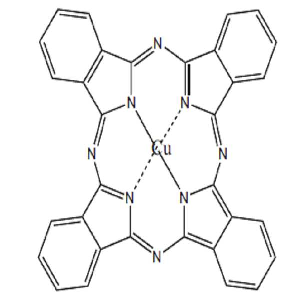
상기 청색 착색제는 청색(blue) 및 청색 계열(bluish)을 띠는 안료(pigment), 또는 상기 안료가 용제에 분산된 분산물을 말하며, 예컨대 상기 안료는 청색 유기안료(Orgainc pigment), 청색 무기안료(Inorganic pigment), 또는 이들의 조합을 포함할 수 있다. 구체적으로, 상기 청색 및 청색 계열을 띠는 안료는 예컨대, C.I. 안료 청색 15호, C.I. 안료 청색 15:3호, C.I. 안료 청색 15:4호, C.I. 안료 청색 15:6호, C.I. 안료 청색 60호, 하기 화학식 1(Indanthrone)로 표시되는 화합물, 하기 화학식 2(Cu-Phthalocyanine)로 표시되는 화합물, 또는 이들의 조합을 포함할 수 있다.The blue colorant refers to a pigment having blue and blue colors, or a dispersion in which the pigment is dispersed in a solvent, for example, the pigment is a blue organic pigment, a blue inorganic pigment (Inorganic pigment), or a combination thereof. Specifically, the blue and blue-based pigments are, for example, C.I. Pigment Blue No. 15, C.I. Pigment Blue 15:3, C.I. Pigment Blue 15:4, C.I. Pigment Blue 15:6, C.I. Pigment Blue No. 60, a compound represented by the following Chemical Formula 1 (Indanthrone), a compound represented by the following Chemical Formula 2 (Cu-Phthalocyanine), or a combination thereof.
[화학식 1][Formula 1]

[화학식 2][Formula 2]
상기 청색 및 청색 계열을 띠는 안료는 상기 바인더 수지에 분산되어 있을 수 있다. 구체적으로 상기 청색 및 청색 계열을 띠는 안료를 상기 바인더 수지가 포함되어 있는 용제에 분산시킬 수 있다. 상기 바인더 수지로는 예컨대 분자량이 작고 OH value값이 높은 PVA/PVC 수지를 사용할 수 있으며, 분산 작업성을 위해 상기 용제로는 예컨대 사이클로헥사논(cyclohexanone)을 사용할 수 있다. 상기 PVA/PVC 수지가 포함되어 있는 상기 용제에 상기 청색 및 청색 계열을 띠는 안료를 Pre-Mixing한 Mill Base를, Ring Mill로 약 1시간 내지 3시간 동안 분산시켜, 상기 바인더 수지에 상기 청색 및 청색 계열을 띠는 안료를 분산시킬 수 있다. 구체적으로, 상기 PVA/PVC 수지 약 30 내지 50 중량%, 상기 사이클로헥사논(cyclohexanone) 용제 약 30 내지 65중량%, 및 상기 청색 착색제 약 5 내지 20 중량%의 중량비로 포함될 수 있다.The blue and blue pigments may be dispersed in the binder resin. Specifically, the blue and blue pigments may be dispersed in a solvent containing the binder resin. As the binder resin, for example, a PVA/PVC resin having a small molecular weight and a high OH value may be used. For the dispersibility, for example, cyclohexanone may be used as the solvent. The mill base obtained by pre-mixing the blue and blue pigments in the solvent containing the PVA/PVC resin is dispersed for about 1 hour to 3 hours with a ring mill, and the blue and The blue-based pigment can be dispersed. Specifically, about 30 to 50% by weight of the PVA/PVC resin, about 30 to 65% by weight of the cyclohexanone solvent, and about 5 to 20% by weight of the blue colorant may be included.
상기 청색 착색제는 후술하는 바와 같이 플라스틱 기재(130), 바인더 층(120) 및 고분자 수지 층(110)을 필름 인서트 방식으로 사출 성형하여 얻어진 사출물의 황색 지수(yellow index, YI)를 보정하여 황색 지수를 낮출 수 있다. 예컨대 상기 사출물의 황색 지수(YI)는 예컨대 약 1.50 이하일 수 있으며, 구체적으로 약 1.0 이하일 수 있다. 이에 따라 표시장치용 윈도우의 황변을 효과적으로 방지하여 투광 특성을 개선할 수 있다.The blue colorant is a yellow index by correcting the yellow index (YI) of the injection material obtained by injection molding the
또한 상기 청색 착색제는 후술하는 바와 같이 플라스틱 기재(130), 바인더 층(120) 및 고분자 수지 층(110)을 필름 인서트 방식으로 사출 성형시 플라스틱 기재(130)와 고분자 수지 층(110) 사이의 접착력을 높일 수 있다. 이에 따라 표시장치용 윈도우의 신뢰성을 개선할 수 있다.In addition, the blue colorant is an adhesive force between the
상기 청색 착색제는 상기 바인더 수지 100 중량%에 대하여 약 0.1 내지 50 중량%로 포함될 수 있다. 상기 범위로 포함됨으로써 황변을 효과적으로 방지하여 투광 특성을 개선할 수 있다. 구체적으로, 상기 청색 착색제는 상기 바인더 수지 100 중량%에 대하여 약 5 내지 20 중량%로 포함될 수 있다.The blue colorant may be included in an amount of about 0.1 to 50% by weight based on 100% by weight of the binder resin. By being included in the above range, it is possible to effectively prevent yellowing and improve light transmission characteristics. Specifically, the blue colorant may be included in about 5 to 20% by weight relative to 100% by weight of the binder resin.
바인더 층(120)은 예컨대 약 5㎛ 내지 10㎛의 두께를 가질 수 있다.
The
하드 코팅층(140)은 플라스틱 기재(130)의 일면에 위치할 수 있다. 하드 코팅층(140)은 예컨대 유기물, 무기물 또는 유무기 복합화합물을 포함할 수 있다. 여기서 상기 유기물은 예컨대 아크릴계 화합물, 에폭시계 화합물, 또는 이들의 조합을 포함할 수 있고, 상기 무기물은 예컨대 실리카, 알루미나, 또는 이들의 조합을 포함할 수 있고, 상기 유무기 복합화합물은 예컨대 폴리실세스퀴옥산을 포함할 수 있다. 하드 코팅층(140)은 단일층 또는 복수층일 수 있으며, 예컨대 약 5㎛ 내지 200㎛의 두께를 가질 수 있다.The
하드 코팅층(140)은 표면 경도가 4H 이상일 수 있다. 여기서 표면 경도는 연필경도 시험기(제조사: BMS Tech)를 사용하여 1kg 하중을 걸고 측정한 결과이다. 상기 범위의 표면 경도를 가짐으로써 표면 스크래치를 방지할 수 있다. The
하드 코팅층(140)은 표시장치용 윈도우(100)의 최상층에 위치하여 표면 경도를 개선할 수 있다. 여기서 표시장치용 윈도우(100)의 최상층에 위치한다는 것은 하드코팅층(140)이 표면 경도에 직접적으로 영향을 미치는 층으로서 최상층에 위치하는 것을 말하며 반사방지막과 같은 추가 기능을 부여하기 위한 층이 추가적으로 위치하는 것을 배제하는 것은 아니다.The
하드 코팅층(140)은 경우에 따라 생략될 수 있다.The
플라스틱 기재(130), 바인더 층(120), 및 고분자 수지 층(110)은 예컨대 IMD 필름(In mold decoration film)일 수 있다.The
표시장치용 윈도우(100)는 플라스틱 기재(130), 바인더 층(120) 및 고분자 수지 층(110)을 필름 인서트 방식으로 사출 성형하여 얻어질 수 있다. The
상기에서는 플라스틱 기재(130) 및 바인더 층(120)이 고분자 수지 층(110)의 일면에 형성된 예만 기재하였지만, 이에 한정되지 않고 고분자 수지 층(110)의 양면에 형성될 수도 있다.In the above, only the example in which the
표시장치용 윈도우(100)는 약 1mm 이하의 두께를 가질 수 있다.The
상술한 표시장치용 윈도우는 다양한 표시 장치에 적용될 수 있다. 표시장치는 액정 표시 장치, 유기 발광 표시 장치, 플라즈마 디스플레이, 전계 효과 표시 장치, 전기 영동 표시 장치 등을 들 수 있으나, 이에 한정되는 것은 아니다.The above-described window for a display device can be applied to various display devices. The display device includes a liquid crystal display device, an organic light emitting display device, a plasma display, a field effect display device, an electrophoretic display device, and the like, but is not limited thereto.
상기 표시장치용 윈도우는 표시 모듈 위에 배치될 수 있으며, 여기서 표시 모듈은 액정 표시 모듈, 유기 발광 표시 모듈, 플라즈마 표시 모듈, 전계 효과 표시 모듈, 전기 영동 표시 모듈 등일 수 있다.The window for the display device may be disposed on the display module, where the display module may be a liquid crystal display module, an organic light emitting display module, a plasma display module, a field effect display module, an electrophoretic display module, or the like.
이하 실시예를 통해서 본 발명을 보다 상세하게 설명한다. 다만 하기의 실시예는 단지 설명의 목적을 위한 것이며 본 발명의 범위를 제한하는 것은 아니다.
The present invention will be described in more detail through the following examples. However, the following examples are for illustrative purposes only and are not intended to limit the scope of the present invention.
바인더 분산액의 제조Preparation of binder dispersion
제조예Manufacturing example 1 One
사이클로헥사논 용제(Cas.No: 108-94-1) 50 중량%에 PVA/PVC 수지(IMB00002, 제국잉크사 제조) 40 중량%와 청색 안료(CSNN Blue, Haubech사 제조) 10 중량%를 첨가한 후, Ring Mill로 2시간 동안 분산시켜 바인더 용액을 제조하였다. (Chiiler 온도 30℃, RPM 1500, bead 100㎛)
40% by weight of PVA/PVC resin (IMB00002, manufactured by Imperial Ink) and 10% by weight of blue pigment (CSNN Blue, manufactured by Haubech) are added to 50% by weight of cyclohexanone solvent (Cas.No: 108-94-1) After that, the binder solution was prepared by dispersing with a ring mill for 2 hours. (Chiiler temperature 30℃, RPM 1500, bead 100㎛)
제조예Manufacturing example 2 2
청색 안료(CSNN Blue, Haubech사 제조) 10 중량% 대신 5 중량%를 사용한 것을 제외하고는 제조예 1과 동일하게 하여 바인더 용액을 제조하였다.
A binder solution was prepared in the same manner as in Preparation Example 1, except that 5% by weight of blue pigment (CSNN Blue, manufactured by Haubech) was used instead of 10% by weight.
제조예Manufacturing example 3 3
청색 안료(CSNN Blue, Haubech사 제조) 10 중량% 대신 20 중량%를 사용한 것을 제외하고는 제조예 1과 동일하게 하여 바인더 용액을 제조하였다.
A binder solution was prepared in the same manner as in Preparation Example 1, except that 20% by weight of blue pigment (CSNN Blue, manufactured by Haubech) was used instead of 10% by weight.
비교 compare 제조예Manufacturing example 1 One
사이클로헥사논 용제(Cas.No: 108-94-1) 50 중량%에 바인더 수지(IMB00002, 제국잉크사 제조) 50 중량%를 첨가하여 바인더 용액을 제조하였다.
A binder solution was prepared by adding 50% by weight of a binder resin (IMB00002, manufactured by Imperial Ink) to 50% by weight of a cyclohexanone solvent (Cas. No: 108-94-1).
비교 compare 제조예Manufacturing example 2 2
사이클로헥사논 용제(Cas.No: 108-94-1) 50 중량%에 PVA/PVC 수지(IMB00002, 제국잉크사 제조) 40 중량%와 백색 안료(R-902, Dupont사 제조) 10 중량%를 첨가한 후, Ring Mill로 2시간 동안 분산시켜 바인더 용액을 제조하였다. (Chiiler 온도 30℃, RPM 1500, bead 100㎛)
40% by weight of PVA/PVC resin (IMB00002, manufactured by Imperial Ink) and 10% by weight of white pigment (R-902, manufactured by Dupont) in 50% by weight of cyclohexanone solvent (Cas.No: 108-94-1) After the addition, the binder solution was prepared by dispersing with a ring mill for 2 hours. (Chiiler temperature 30℃, RPM 1500, bead 100㎛)
표시장치용 Display device 윈도우의Windows 제작 making
실시예Example 1 One
PET 필름(PET100A4300, TOYOBO사 제조)의 일면에 폴리실세스퀴옥산 용액(Radisol-S, ㈜성원소재)을 도포하고 80℃에서 1분간 건조한 후 자외선을 조사(300mJ/㎠)하여 경화하였다. 이어서 상기 PET 필름의 다른 일면에 상기 제조예 1의 바인더 용액을 도포하여 100℃에서 10분간 건조하였다. 이어서 100℃에서 선경화하였다. 이어서 상기 PET 필름을 사출 성형기에 넣고 하기 폴리카보네이트(PC)(HFD1810, Sabic사)를 사출 성형하여 0.79mm의 폴리카보네이트(PC) 수지층을 포함하는 1mm 두께의 표시장치용 윈도우를 제작하였다. 각 층의 두께는 아래와 같다.A polysilsesquioxane solution (Radisol-S, Sungwon Materials Co., Ltd.) was applied to one surface of the PET film (PET100A4300, manufactured by TOYOBO), dried at 80° C. for 1 minute, and then irradiated with ultraviolet light (300 mJ/cm 2) to cure. Subsequently, the binder solution of Preparation Example 1 was applied to the other surface of the PET film and dried at 100°C for 10 minutes. It was then pre-cured at 100°C. Subsequently, the PET film was placed in an injection molding machine, and injection molding of the following polycarbonate (PC) (HFD1810, Sabic) was performed to prepare a window for a display device having a thickness of 1 mm including a 0.79 mm polycarbonate (PC) resin layer. The thickness of each layer is as follows.
하드 코팅층: 0.15mmHard coating layer: 0.15mm
PET 필름: 0.05mmPET film: 0.05mm
바인더 층: 0.01mmBinder layer: 0.01mm
폴리카보네이트(PC) 수지층: 0.79mm
Polycarbonate (PC) resin layer: 0.79 mm
실시예Example 2 2
상기 제조예 1의 바인더 용액 대신 상기 제조예 2의 바인더 용액을 사용한 것을 제외하고는 실시예 1과 동일한 방법으로 수행하여 1mm 두께의 표시장치용 윈도우를 제작하였다. 각 층의 두께는 아래와 같다.A window for a display device having a thickness of 1 mm was manufactured in the same manner as in Example 1, except that the binder solution of Preparation Example 2 was used instead of the binder solution of Preparation Example 1. The thickness of each layer is as follows.
하드 코팅층: 0.15mmHard coating layer: 0.15mm
PET 필름: 0.05mmPET film: 0.05mm
바인더 층: 0.01mmBinder layer: 0.01mm
폴리카보네이트(PC) 수지층: 0.79mm
Polycarbonate (PC) resin layer: 0.79 mm
실시예Example 3 3
상기 제조예 1의 바인더 용액 대신 상기 제조예 3의 바인더 용액을 사용한 것을 제외하고는 실시예 1과 동일한 방법으로 수행하여 1mm 두께의 표시장치용 윈도우를 제작하였다. 각 층의 두께는 아래와 같다.A window for a display device having a thickness of 1 mm was manufactured in the same manner as in Example 1, except that the binder solution of Preparation Example 3 was used instead of the binder solution of Preparation Example 1. The thickness of each layer is as follows.
하드 코팅층: 0.15mmHard coating layer: 0.15mm
PET 필름: 0.05mmPET film: 0.05mm
바인더 층: 0.01mmBinder layer: 0.01mm
폴리카보네이트(PC) 수지층: 0.79mm
Polycarbonate (PC) resin layer: 0.79 mm
비교예Comparative example 1 One
상기 제조예 1의 바인더 용액 대신 상기 비교 제조예 1의 바인더 용액을 사용한 것을 제외하고는 실시예 1과 동일한 방법으로 수행하여 1mm 두께의 표시장치용 윈도우를 제작하였다. 각 층의 두께는 아래와 같다.A window for a display device having a thickness of 1 mm was manufactured in the same manner as in Example 1, except that the binder solution of Comparative Preparation Example 1 was used instead of the binder solution of Preparation Example 1. The thickness of each layer is as follows.
하드 코팅층: 0.15mmHard coating layer: 0.15mm
PET 필름: 0.05mmPET film: 0.05mm
바인더 층: 0.01mmBinder layer: 0.01mm
폴리카보네이트(PC) 수지층: 0.79mm
Polycarbonate (PC) resin layer: 0.79 mm
비교예Comparative example 2 2
상기 폴리카보네이트(PC) 수지층 대신 폴리메틸메타크릴레이트(PMMA) 수지층을 사용한 것을 제외하고는 비교예 1과 동일한 방법으로 수행하여 1mm 두께의 표시장치용 윈도우를 제작하였다. 각 층의 두께는 아래와 같다.A window for a display device having a thickness of 1 mm was manufactured in the same manner as in Comparative Example 1, except that a polymethyl methacrylate (PMMA) resin layer was used instead of the polycarbonate (PC) resin layer. The thickness of each layer is as follows.
하드 코팅층: 0.15mmHard coating layer: 0.15mm
PET 필름: 0.05mmPET film: 0.05mm
바인더 층: 0.01mmBinder layer: 0.01mm
폴리메틸메타크릴레이트(PMMA) 수지층: 0.79mm
Polymethyl methacrylate (PMMA) resin layer: 0.79 mm
비교예Comparative example 3 3
상기 제조예 1의 바인더 용액 대신 상기 비교 제조예 2의 바인더 용액을 사용한 것을 제외하고는 실시예 1과 동일한 방법으로 수행하여 1mm 두께의 표시장치용 윈도우를 제작하였다. 각 층의 두께는 아래와 같다.A window for a display device having a thickness of 1 mm was manufactured in the same manner as in Example 1, except that the binder solution of Comparative Preparation Example 2 was used instead of the binder solution of Preparation Example 1. The thickness of each layer is as follows.
하드 코팅층: 0.15mmHard coating layer: 0.15mm
PET 필름: 0.05mmPET film: 0.05mm
바인더 층: 0.01mmBinder layer: 0.01mm
폴리카보네이트(PC) 수지층: 0.79mm
Polycarbonate (PC) resin layer: 0.79 mm
평가evaluation
실시예 1 내지 3과 비교예 1 내지 3에 따른 표시장치용 윈도우의 광특성(YI값) 및 신뢰성(접착력)을 평가하였다.The optical properties (YI value) and reliability (adhesive power) of the window for a display device according to Examples 1 to 3 and Comparative Examples 1 to 3 were evaluated.
YI값은 MINOLTA CM-3600D를 사용하여 측정하였다. 측정기준은 D1925 illuminant 550nm영역에서의 Yellow Index값을 측정하였다.The YI value was measured using MINOLTA CM-3600D. As a measurement standard, the Yellow Index value in the D1925 illuminant 550nm region was measured.
접착력은 85℃의 온도, 85%의 습도에서 각각의 시간대(초기(0h), 24h, 48h, 72h, 96h, 120h)별로 필름 박리유무를 육안으로 평가하였다.Adhesion was evaluated visually for the presence or absence of film peeling at each temperature (initial (0h), 24h, 48h, 72h, 96h, 120h) at a temperature of 85°C and humidity of 85%.
그 결과는 표 1과 같다.
Table 1 shows the results.
필름 두께 (mm)Translucent
Film thickness (mm)
(mm)Window thickness
(mm)
(0HR)Early
(0HR)
표 1을 참고하면, 실시예 1 내지 3에 따른 표시장치용 윈도우는 광특성 및 (접착)신뢰성이 양호한 것을 확인할 수 있다. 이에 반해, 청색 안료가 분산되지 않은 바인더를 사용한 비교예 1 및 2는 광특성 및 (접착)신뢰성이 불량하고, 백색 안료가 분산된 바인더를 사용한 비교예 3은 접착 특성은 양호하나 광특성이 불량한 것으로 평가되었다. 상기 결과로부터 청색 안료가 분산된 바인더를 포함하는 플라스틱 윈도우는 광특성 경도 및 (접착)신뢰성을 모두 만족하는 것을 확인할 수 있다.
Referring to Table 1, it can be seen that the window for a display device according to Examples 1 to 3 has good optical characteristics and (adhesive) reliability. On the other hand, Comparative Examples 1 and 2 using the binder in which the blue pigment was not dispersed had poor optical properties and (adhesive) reliability, and Comparative Example 3 using the binder in which the white pigment was dispersed had good adhesive properties but poor optical properties. Was evaluated. From the above results, it can be seen that the plastic window including the binder in which the blue pigment is dispersed satisfies both optical property hardness and (adhesive) reliability.
이상에서 본 발명의 바람직한 실시예들에 대하여 상세하게 설명하였지만 본 발명의 권리 범위는 이에 한정되는 것은 아니고 다음의 청구 범위에서 정의하고 있는 본 발명의 기본 개념을 이용한 당업자의 여러 변형 및 개량 형태 또한 본 발명의 권리 범위에 속하는 것이다.
Although preferred embodiments of the present invention have been described in detail above, the scope of rights of the present invention is not limited thereto, and various modifications and improvements of those skilled in the art using the basic concept of the present invention defined in the following claims are also provided. It belongs to the scope of the invention.
100: 표시장치용 윈도우
110: 고분자 수지 층
120: 바인더 층
130: 플라스틱 기재
140: 하드 코팅층100: display window
110: polymer resin layer
120: binder layer
130: plastic substrate
140: hard coating layer
Claims (17)
상기 플라스틱 기재의 일면에 위치하는 고분자 수지 층, 및
상기 플라스틱 기재와 상기 고분자 수지층 사이에 위치하는 바인더 층
을 포함하고,
상기 바인더 층은 바인더 수지 및 청색 착색제를 포함하고,
상기 청색 착색제는 상기 바인더 수지 100 중량%에 대하여 5 내지 20 중량%가 분산되며,
표시장치용 윈도우는 YI(Yellow Index)값이 1.00 이하인 표시장치용 윈도우.
Plastic substrate,
A polymer resin layer located on one surface of the plastic substrate, and
A binder layer positioned between the plastic substrate and the polymer resin layer
Including,
The binder layer includes a binder resin and a blue colorant,
The blue colorant is dispersed 5 to 20% by weight relative to 100% by weight of the binder resin,
The window for the display device is a window for a display device having a YI (Yellow Index) value of 1.00 or less.
상기 고분자 수지 층은 폴리카보네이트(PC), 폴리메틸메타크릴레이트(PMMA), 사이클로올레핀중합체(COP), 폴리에틸렌테레프탈레이트(PET), 이들의 공중합체 및 이들의 조합에서 선택된 고분자를 포함하는 표시장치용 윈도우.
According to claim 1,
The polymer resin layer is a display device comprising a polymer selected from polycarbonate (PC), polymethyl methacrylate (PMMA), cycloolefin polymer (COP), polyethylene terephthalate (PET), copolymers thereof, and combinations thereof For Windows.
상기 고분자 수지 층은 700㎛ 내지 940㎛의 두께를 가지는 표시장치용 윈도우.
According to claim 1,
The polymer resin layer is a window for a display device having a thickness of 700㎛ to 940㎛.
상기 플라스틱 기재는 폴리에틸렌테레프탈레이트(PET) 필름, 폴리카보네이트(PC) 필름, 폴리메틸메타크릴레이트(PMMA) 필름, 폴리카보네이트/폴리메틸메타크릴레이트(PC/PMMA) 필름, 또는 이들의 조합을 포함하는 표시장치용 윈도우.
According to claim 1,
The plastic substrate includes a polyethylene terephthalate (PET) film, a polycarbonate (PC) film, a polymethyl methacrylate (PMMA) film, a polycarbonate/polymethyl methacrylate (PC/PMMA) film, or a combination thereof Windows for display devices.
상기 플라스틱 기재 및 상기 바인더 층은 각각 50㎛ 내지 100㎛와 5㎛ 내지 10㎛의 두께를 가지는 표시장치용 윈도우.
According to claim 1,
The plastic substrate and the binder layer have a window for a display device having a thickness of 50㎛ to 100㎛ and 5㎛ to 10㎛, respectively.
상기 플라스틱 기재의 일면에 위치하는 하드 코팅층을 더 포함하는 표시장치용 윈도우.
According to claim 1,
A window for a display device further comprising a hard coating layer positioned on one surface of the plastic substrate.
상기 하드 코팅층은 유기물, 무기물 또는 유무기 복합화합물을 포함하는 표시장치용 윈도우.
The method of claim 8,
The hard coating layer is a window for a display device comprising an organic, inorganic or organic-inorganic composite compound.
상기 하드 코팅층은 표면 경도가 4H 이상인 표시장치용 윈도우.
The method of claim 8,
The hard coating layer is a window for a display device having a surface hardness of 4H or more.
상기 하드 코팅층은 5㎛ 내지 200㎛의 두께를 가지는 표시장치용 윈도우.
The method of claim 8,
The hard coating layer is a window for a display device having a thickness of 5㎛ to 200㎛.
상기 플라스틱 기재, 상기 바인더 층 및 상기 고분자 수지 층은 IMD(In mold decoration) 필름인 표시장치용 윈도우.
According to claim 1,
The plastic substrate, the binder layer and the polymer resin layer is an IMD (In mold decoration) film display window.
상기 표시장치용 윈도우는 상기 플라스틱 기재, 상기 바인더 층 및 상기 고분자 수지를 필름 인서트 방식으로 사출 성형하여 얻어지는 표시장치용 윈도우.
According to claim 1,
The window for the display device is a window for a display device obtained by injection molding the plastic substrate, the binder layer and the polymer resin by a film insert method.
상기 표시장치용 윈도우는 1mm 이하의 두께를 가지는 표시장치용 윈도우.
According to claim 1,
The window for the display device has a thickness of 1mm or less.
Priority Applications (4)
| Application Number | Priority Date | Filing Date | Title |
|---|---|---|---|
| KR1020130062050A KR102130700B1 (en) | 2013-05-30 | 2013-05-30 | Window for display device and display device including the window |
| US14/014,614 US9604434B2 (en) | 2013-05-30 | 2013-08-30 | Window for display device and display device including the window |
| TW102137048A TWI629178B (en) | 2013-05-30 | 2013-10-15 | Window for display device, method of manufacturing the same, and display device including the window |
| CN201310613140.1A CN104210199B (en) | 2013-05-30 | 2013-11-27 | Window for display device and display device including the same |
Applications Claiming Priority (1)
| Application Number | Priority Date | Filing Date | Title |
|---|---|---|---|
| KR1020130062050A KR102130700B1 (en) | 2013-05-30 | 2013-05-30 | Window for display device and display device including the window |
Publications (2)
| Publication Number | Publication Date |
|---|---|
| KR20140140961A KR20140140961A (en) | 2014-12-10 |
| KR102130700B1 true KR102130700B1 (en) | 2020-07-07 |
Family
ID=51985422
Family Applications (1)
| Application Number | Title | Priority Date | Filing Date |
|---|---|---|---|
| KR1020130062050A Active KR102130700B1 (en) | 2013-05-30 | 2013-05-30 | Window for display device and display device including the window |
Country Status (4)
| Country | Link |
|---|---|
| US (1) | US9604434B2 (en) |
| KR (1) | KR102130700B1 (en) |
| CN (1) | CN104210199B (en) |
| TW (1) | TWI629178B (en) |
Families Citing this family (36)
| Publication number | Priority date | Publication date | Assignee | Title |
|---|---|---|---|---|
| US9938012B1 (en) * | 2013-11-25 | 2018-04-10 | Michael C. Kollias | Collapsible article organizer for airliner use |
| US20160351465A1 (en) * | 2015-06-01 | 2016-12-01 | Lead-Honor Optronics Co., Ltd. | Assembly layer structure used in touch control integrated circuit (ic) module and manufacturing method thereof |
| KR20170111422A (en) * | 2016-03-28 | 2017-10-12 | 주식회사 에스티이케이 | Display protection film for shock absorbing |
| US10773952B2 (en) | 2016-05-20 | 2020-09-15 | Qorvo Us, Inc. | Wafer-level package with enhanced performance |
| US10784149B2 (en) | 2016-05-20 | 2020-09-22 | Qorvo Us, Inc. | Air-cavity module with enhanced device isolation |
| CN116884928A (en) | 2016-08-12 | 2023-10-13 | Qorvo美国公司 | Wafer-level packaging with enhanced performance |
| US10109502B2 (en) | 2016-09-12 | 2018-10-23 | Qorvo Us, Inc. | Semiconductor package with reduced parasitic coupling effects and process for making the same |
| KR102452649B1 (en) * | 2016-10-21 | 2022-10-07 | 삼성전자주식회사 | Stacked transparent film and window for display device and display device |
| US10749518B2 (en) * | 2016-11-18 | 2020-08-18 | Qorvo Us, Inc. | Stacked field-effect transistor switch |
| US10068831B2 (en) | 2016-12-09 | 2018-09-04 | Qorvo Us, Inc. | Thermally enhanced semiconductor package and process for making the same |
| KR102009962B1 (en) * | 2017-02-03 | 2019-08-12 | 동우 화인켐 주식회사 | Hard coating film and flexible display window including a touch semsor using the same |
| US10755992B2 (en) | 2017-07-06 | 2020-08-25 | Qorvo Us, Inc. | Wafer-level packaging for enhanced performance |
| US10784233B2 (en) | 2017-09-05 | 2020-09-22 | Qorvo Us, Inc. | Microelectronics package with self-aligned stacked-die assembly |
| US11152363B2 (en) | 2018-03-28 | 2021-10-19 | Qorvo Us, Inc. | Bulk CMOS devices with enhanced performance and methods of forming the same utilizing bulk CMOS process |
| US12062700B2 (en) | 2018-04-04 | 2024-08-13 | Qorvo Us, Inc. | Gallium-nitride-based module with enhanced electrical performance and process for making the same |
| US12046505B2 (en) | 2018-04-20 | 2024-07-23 | Qorvo Us, Inc. | RF devices with enhanced performance and methods of forming the same utilizing localized SOI formation |
| US10804246B2 (en) | 2018-06-11 | 2020-10-13 | Qorvo Us, Inc. | Microelectronics package with vertically stacked dies |
| EP3818558A1 (en) | 2018-07-02 | 2021-05-12 | Qorvo US, Inc. | Rf semiconductor device and manufacturing method thereof |
| US10964554B2 (en) | 2018-10-10 | 2021-03-30 | Qorvo Us, Inc. | Wafer-level fan-out package with enhanced performance |
| US11069590B2 (en) | 2018-10-10 | 2021-07-20 | Qorvo Us, Inc. | Wafer-level fan-out package with enhanced performance |
| US11646242B2 (en) | 2018-11-29 | 2023-05-09 | Qorvo Us, Inc. | Thermally enhanced semiconductor package with at least one heat extractor and process for making the same |
| CN109686476B (en) * | 2019-01-04 | 2020-06-12 | 深圳市华科创智技术有限公司 | Silver nanowire transparent conductive film capable of reducing yellowness |
| KR102621625B1 (en) | 2019-01-04 | 2024-01-05 | 삼성전자주식회사 | Electronic device having housing |
| US12046570B2 (en) | 2019-01-23 | 2024-07-23 | Qorvo Us, Inc. | RF devices with enhanced performance and methods of forming the same |
| US12046483B2 (en) | 2019-01-23 | 2024-07-23 | Qorvo Us, Inc. | RF devices with enhanced performance and methods of forming the same |
| US11387157B2 (en) | 2019-01-23 | 2022-07-12 | Qorvo Us, Inc. | RF devices with enhanced performance and methods of forming the same |
| US12125825B2 (en) | 2019-01-23 | 2024-10-22 | Qorvo Us, Inc. | RF devices with enhanced performance and methods of forming the same |
| EP3915134A1 (en) | 2019-01-23 | 2021-12-01 | Qorvo US, Inc. | Rf semiconductor device and manufacturing method thereof |
| US12057374B2 (en) | 2019-01-23 | 2024-08-06 | Qorvo Us, Inc. | RF devices with enhanced performance and methods of forming the same |
| US12074086B2 (en) | 2019-11-01 | 2024-08-27 | Qorvo Us, Inc. | RF devices with nanotube particles for enhanced performance and methods of forming the same |
| US11646289B2 (en) | 2019-12-02 | 2023-05-09 | Qorvo Us, Inc. | RF devices with enhanced performance and methods of forming the same |
| US11923238B2 (en) | 2019-12-12 | 2024-03-05 | Qorvo Us, Inc. | Method of forming RF devices with enhanced performance including attaching a wafer to a support carrier by a bonding technique without any polymer adhesive |
| US12129168B2 (en) | 2019-12-23 | 2024-10-29 | Qorvo Us, Inc. | Microelectronics package with vertically stacked MEMS device and controller device |
| CN115885333A (en) * | 2020-09-29 | 2023-03-31 | 三星电子株式会社 | Electronic devices including flexible displays |
| EP4260369A2 (en) | 2020-12-11 | 2023-10-18 | Qorvo US, Inc. | Multi-level 3d stacked package and methods of forming the same |
| US12062571B2 (en) | 2021-03-05 | 2024-08-13 | Qorvo Us, Inc. | Selective etching process for SiGe and doped epitaxial silicon |
Citations (1)
| Publication number | Priority date | Publication date | Assignee | Title |
|---|---|---|---|---|
| JP2006319251A (en) * | 2005-05-16 | 2006-11-24 | Dainippon Printing Co Ltd | Composite electromagnetic wave shield filter |
Family Cites Families (11)
| Publication number | Priority date | Publication date | Assignee | Title |
|---|---|---|---|---|
| JPH01197570A (en) * | 1988-02-01 | 1989-08-09 | Daikin Ind Ltd | Low-refractive index hard coating agent |
| US6811867B1 (en) * | 2000-02-10 | 2004-11-02 | 3M Innovative Properties Company | Color stable pigmented polymeric films |
| WO2006120887A1 (en) | 2005-05-12 | 2006-11-16 | Nippon Kayaku Kabushiki Kaisha | Photosensitive resin compositions, cured articles of the compositions, and films containing the compositions |
| JP2007152886A (en) | 2005-12-08 | 2007-06-21 | Fujifilm Corp | Laminated sheet and manufacturing method thereof |
| CN100487499C (en) * | 2006-08-31 | 2009-05-13 | 甘国工 | Optical filter having electromagnetic radiation prevention and light filtering function of plasma display |
| CN100462749C (en) * | 2006-08-31 | 2009-02-18 | 甘国工 | Filter plate having electromagnetic radiation prevention and light filtering function of plasma display |
| KR20090016925A (en) * | 2007-08-13 | 2009-02-18 | 박철 | Spin Window Fabrication Structure |
| JP5401030B2 (en) | 2007-11-27 | 2014-01-29 | 住友化学株式会社 | Extruded resin film and method for producing the same |
| JP5325616B2 (en) | 2009-03-13 | 2013-10-23 | 嶋田プレシジョン株式会社 | Film insert molded product, manufacturing method thereof, and liquid crystal display device including the same |
| JP5120728B2 (en) | 2009-05-14 | 2013-01-16 | 住友化学株式会社 | Polarizing plate, and liquid crystal panel and liquid crystal display device using the same |
| KR101311404B1 (en) * | 2009-08-11 | 2013-09-25 | 박준영 | Touch panel |
-
2013
- 2013-05-30 KR KR1020130062050A patent/KR102130700B1/en active Active
- 2013-08-30 US US14/014,614 patent/US9604434B2/en active Active
- 2013-10-15 TW TW102137048A patent/TWI629178B/en active
- 2013-11-27 CN CN201310613140.1A patent/CN104210199B/en active Active
Patent Citations (1)
| Publication number | Priority date | Publication date | Assignee | Title |
|---|---|---|---|---|
| JP2006319251A (en) * | 2005-05-16 | 2006-11-24 | Dainippon Printing Co Ltd | Composite electromagnetic wave shield filter |
Also Published As
| Publication number | Publication date |
|---|---|
| TW201444692A (en) | 2014-12-01 |
| TWI629178B (en) | 2018-07-11 |
| CN104210199B (en) | 2020-12-01 |
| CN104210199A (en) | 2014-12-17 |
| KR20140140961A (en) | 2014-12-10 |
| US20140356602A1 (en) | 2014-12-04 |
| US9604434B2 (en) | 2017-03-28 |
Similar Documents
| Publication | Publication Date | Title |
|---|---|---|
| KR102130700B1 (en) | Window for display device and display device including the window | |
| TWI381196B (en) | A polarizing plate, a method for manufacturing the same, an optical film, and an image display device | |
| KR20150004496A (en) | Window for display device and display device including the window panel | |
| KR101823713B1 (en) | Scattering protecting film with excellent optical properties and scratch resistance and method of manufacturing the same | |
| KR20140124078A (en) | Window for display device and display device including the window panel | |
| US9423639B2 (en) | Window for display device and display device including the window | |
| KR102346796B1 (en) | Cover window plate and manufacturing method thereof | |
| EP3951452A1 (en) | Anti-reflection circular polariser and image display device using same | |
| US20140315007A1 (en) | Window for display device and display device including the window | |
| KR102087966B1 (en) | Window for display device and display device including the window | |
| WO2011024783A1 (en) | Intermediate film for laminated glass, and laminated glass | |
| KR20200101037A (en) | Preparation Method for Polarizing Plate | |
| KR101791232B1 (en) | Plastic film laminate | |
| KR20140117179A (en) | Window for display device and display device including the window | |
| KR102346783B1 (en) | Cover window plate and image display device having the same | |
| KR20160080277A (en) | Multi-layer sheet | |
| KR20150048042A (en) | Transparent conductor, method for preparing the same and optical display apparatus comprising the same | |
| KR20140142564A (en) | Window for display device and display device including the window panel | |
| US20150029648A1 (en) | Window panel, manufacturing method thereof, and display apparatus including the window panel | |
| KR102758010B1 (en) | Multilayer sheet and multilayer electronic device | |
| KR20130046618A (en) | Diffusing sheet for a back light unit and the manufacturing method thereof | |
| KR20140119860A (en) | Window for display device and display device including the window | |
| KR102527596B1 (en) | Thermochromic decoration and anti-scattering film, laminate and display device | |
| JP2014228829A (en) | Antireflection film | |
| KR20240061648A (en) | Micro LED image display device |
Legal Events
| Date | Code | Title | Description |
|---|---|---|---|
| PA0109 | Patent application |
Patent event code: PA01091R01D Comment text: Patent Application Patent event date: 20130530 |
|
| PG1501 | Laying open of application | ||
| A201 | Request for examination | ||
| PA0201 | Request for examination |
Patent event code: PA02012R01D Patent event date: 20180504 Comment text: Request for Examination of Application Patent event code: PA02011R01I Patent event date: 20130530 Comment text: Patent Application |
|
| E902 | Notification of reason for refusal | ||
| PE0902 | Notice of grounds for rejection |
Comment text: Notification of reason for refusal Patent event date: 20190903 Patent event code: PE09021S01D |
|
| AMND | Amendment | ||
| E601 | Decision to refuse application | ||
| PE0601 | Decision on rejection of patent |
Patent event date: 20200303 Comment text: Decision to Refuse Application Patent event code: PE06012S01D Patent event date: 20190903 Comment text: Notification of reason for refusal Patent event code: PE06011S01I |
|
| X091 | Application refused [patent] | ||
| AMND | Amendment | ||
| PX0901 | Re-examination |
Patent event code: PX09011S01I Patent event date: 20200303 Comment text: Decision to Refuse Application Patent event code: PX09012R01I Patent event date: 20191101 Comment text: Amendment to Specification, etc. |
|
| PX0701 | Decision of registration after re-examination |
Patent event date: 20200406 Comment text: Decision to Grant Registration Patent event code: PX07013S01D Patent event date: 20200402 Comment text: Amendment to Specification, etc. Patent event code: PX07012R01I Patent event date: 20200303 Comment text: Decision to Refuse Application Patent event code: PX07011S01I Patent event date: 20191101 Comment text: Amendment to Specification, etc. Patent event code: PX07012R01I |
|
| X701 | Decision to grant (after re-examination) | ||
| GRNT | Written decision to grant | ||
| PR0701 | Registration of establishment |
Comment text: Registration of Establishment Patent event date: 20200630 Patent event code: PR07011E01D |
|
| PR1002 | Payment of registration fee |
Payment date: 20200630 End annual number: 3 Start annual number: 1 |
|
| PG1601 | Publication of registration | ||
| PR1001 | Payment of annual fee |
Payment date: 20230524 Start annual number: 4 End annual number: 4 |