KR102049076B1 - non- volatile memory device and operating method thereof - Google Patents
non- volatile memory device and operating method thereof Download PDFInfo
- Publication number
- KR102049076B1 KR102049076B1 KR1020120140998A KR20120140998A KR102049076B1 KR 102049076 B1 KR102049076 B1 KR 102049076B1 KR 1020120140998 A KR1020120140998 A KR 1020120140998A KR 20120140998 A KR20120140998 A KR 20120140998A KR 102049076 B1 KR102049076 B1 KR 102049076B1
- Authority
- KR
- South Korea
- Prior art keywords
- memory device
- memory cells
- data
- nonvolatile memory
- string
- Prior art date
- Legal status (The legal status is an assumption and is not a legal conclusion. Google has not performed a legal analysis and makes no representation as to the accuracy of the status listed.)
- Active
Links
Images


Classifications
-
- G—PHYSICS
- G11—INFORMATION STORAGE
- G11C—STATIC STORES
- G11C16/00—Erasable programmable read-only memories
- G11C16/02—Erasable programmable read-only memories electrically programmable
- G11C16/06—Auxiliary circuits, e.g. for writing into memory
-
- G—PHYSICS
- G11—INFORMATION STORAGE
- G11C—STATIC STORES
- G11C29/00—Checking stores for correct operation ; Subsequent repair; Testing stores during standby or offline operation
- G11C29/70—Masking faults in memories by using spares or by reconfiguring
- G11C29/78—Masking faults in memories by using spares or by reconfiguring using programmable devices
- G11C29/80—Masking faults in memories by using spares or by reconfiguring using programmable devices with improved layout
- G11C29/816—Masking faults in memories by using spares or by reconfiguring using programmable devices with improved layout for an application-specific layout
- G11C29/82—Masking faults in memories by using spares or by reconfiguring using programmable devices with improved layout for an application-specific layout for EEPROMs
-
- G—PHYSICS
- G11—INFORMATION STORAGE
- G11C—STATIC STORES
- G11C16/00—Erasable programmable read-only memories
- G11C16/02—Erasable programmable read-only memories electrically programmable
- G11C16/04—Erasable programmable read-only memories electrically programmable using variable threshold transistors, e.g. FAMOS
- G11C16/0483—Erasable programmable read-only memories electrically programmable using variable threshold transistors, e.g. FAMOS comprising cells having several storage transistors connected in series
-
- G—PHYSICS
- G11—INFORMATION STORAGE
- G11C—STATIC STORES
- G11C16/00—Erasable programmable read-only memories
- G11C16/02—Erasable programmable read-only memories electrically programmable
- G11C16/06—Auxiliary circuits, e.g. for writing into memory
- G11C16/10—Programming or data input circuits
-
- G—PHYSICS
- G11—INFORMATION STORAGE
- G11C—STATIC STORES
- G11C16/00—Erasable programmable read-only memories
- G11C16/02—Erasable programmable read-only memories electrically programmable
- G11C16/06—Auxiliary circuits, e.g. for writing into memory
- G11C16/34—Determination of programming status, e.g. threshold voltage, overprogramming or underprogramming, retention
- G11C16/3436—Arrangements for verifying correct programming or erasure
- G11C16/344—Arrangements for verifying correct erasure or for detecting overerased cells
Landscapes
- Engineering & Computer Science (AREA)
- Microelectronics & Electronic Packaging (AREA)
- Read Only Memory (AREA)
- Theoretical Computer Science (AREA)
- Semiconductor Memories (AREA)
- Physics & Mathematics (AREA)
- General Engineering & Computer Science (AREA)
- General Physics & Mathematics (AREA)
Abstract
본 발명은 비휘발성 메모리 장치를 제어하는 메모리 컨트롤러의 구동 방법에 관한 것이다. 상기 비휘발성 메모리 장치는 기판과 수직 방향으로 배열되는 복수의 메모리 셀을 포함하고, 상기 비휘발성 메모리 장치의 동작을 제어하는 메모리 컨트롤러의 동작 방법은, 상기 복수의 메모리 셀을 소거 상태로 만들고, 제 1 워드 라인 전압을 사용하여 제 1 워드 라인에 연결된 메모리 셀들을 읽고 오프 상태인 메모리 셀들에 대응되는 스트링 주소 정보를 서치하고, 상기 스트링 주소 정보를 참조하여 상기 스트링 주소 정보에 대응되는 해당 메모리 셀들을 특정 프로그램 상태로 프로그램하고 맵핑 정보를 저장하는 것을 포함한다. The present invention relates to a method of driving a memory controller for controlling a nonvolatile memory device. The nonvolatile memory device includes a plurality of memory cells arranged in a direction perpendicular to a substrate, and an operating method of a memory controller for controlling an operation of the nonvolatile memory device includes: putting the plurality of memory cells in an erased state; Read the memory cells connected to the first word line using one word line voltage, search string address information corresponding to the memory cells in an off state, and search the corresponding memory cells corresponding to the string address information with reference to the string address information. Programming to a specific program state and storing mapping information.
Description
본 발명은 비휘발성 메모리 장치에 관한 것으로, 좀 더 구체적으로는 3차원 비휘발성 메모리 장치의 동작 방법에 관한 것이다.The present invention relates to a nonvolatile memory device, and more particularly to a method of operating a three-dimensional nonvolatile memory device.
메모리 장치는 휘발성(volatile) 메모리 장치와 비휘발성(non-volatile) 메모리 장치로 분류된다. 휘발성 메모리 장치는 전원(power)이 제거될 때 데이터는 유지되지 않는다. 그러나 비휘발성 메모리 장치는 전원이 제거되더라도 데이터는 유지된다.
비휘발성 메모리 장치의 예들로서 ROM(read only memory), 또는 EEPROM (Electrically Erasable Programmable Read-Only Memory) 등이 있다.
플래시(flash) EEPROM으로 소개된 플래시 메모리 장치의 구조와 동작은 종래의 EEPROM의 구조와 동작과 서로 다르다. 플래시 메모리 장치는 블락(block) 단위로 전기적 소거(electric erase) 동작을 수행하고 비트 단위로 프로그램 동작을 수행할 수 있다.
플래시 메모리 장치에 포함된 프로그램된 다수개의 메모리 셀들의 문턱 전압들(threshold voltages)은 여러 가지 원인, 예컨대 플로팅 게이트 커플링 (floating gate coupling), 시간의 경과에 따른 전하 손실(charge loss), 등에 따라 변할 수 있다. 플래시 메모리 장치는 기판과 수직방향으로 배열되는 메모리 셀들을 포함하는 3차원 구조로 구성될 수 있다. Memory devices are classified into volatile memory devices and non-volatile memory devices. Volatile memory devices do not retain data when power is removed. However, nonvolatile memory devices retain their data even when their power sources are removed.
Examples of nonvolatile memory devices include read only memory (ROM) or electrically erasable programmable read-only memory (EEPROM).
The structure and operation of a flash memory device introduced as a flash EEPROM is different from that of a conventional EEPROM. The flash memory device may perform an electric erase operation in units of blocks and a program operation in units of bits.
Threshold voltages of a plurality of programmed memory cells included in a flash memory device may be caused by various causes, such as floating gate coupling, charge loss over time, and the like. Can change. The flash memory device may have a three-dimensional structure including memory cells arranged in a direction perpendicular to the substrate.
본 발명이 해결하려는 과제는 3차원 플래시 메모리 장치에서 공정상의 결함으로 채널이 형성되지 않음으로 발생하는 에러 비트를 정정하는 데 있다.
본 발명이 해결하려는 과제들은 이상에서 언급한 과제들로 제한되지 않으며, 언급되지 않은 또 다른 과제들은 아래의 기재로부터 당업자에게 명확하게 이해될 수 있을 것이다.The problem to be solved by the present invention is to correct the error bit caused by not forming a channel due to a process defect in a three-dimensional flash memory device.
Problems to be solved by the present invention are not limited to the above-mentioned problems, and other problems not mentioned will be clearly understood by those skilled in the art from the following description.
본 발명은 비휘발성 메모리 장치를 제어하는 메모리 컨트롤러의 구동 방법에 관한 것이다. 상기 비휘발성 메모리 장치는 기판과 수직 방향으로 배열되는 복수의 메모리 셀을 포함하고, 상기 비휘발성 메모리 장치의 동작을 제어하는 메모리 컨트롤러의 동작 방법은, 상기 복수의 메모리 셀을 소거 상태로 만들고, 제 1 워드 라인 전압을 사용하여 제 1 워드 라인에 연결된 메모리 셀들을 읽고 오프 상태인 메모리 셀들에 대응되는 스트링 주소 정보를 서치하고, 상기 스트링 주소 정보를 참조하여 상기 스트링 주소 정보에 대응되는 해당 메모리 셀들을 특정 프로그램 상태로 프로그램하고 맵핑 정보를 저장하는 것을 포함한다.
본 발명의 다른 일면은 비휘발성 메모리 장치의 구동 방법에 관한 것이다. 상기 비휘발성 메모리 장치는 기판과 수직방향으로 배열되고 메모리 셀들, 스트링 선택 트랜지스터와 접지 선택 트랜지스터를 포함하는 셀 스트링을 적어도 하나 이상 갖는다. 비휘발성 메모리 장치의 동작 방법은, 상기 메모리 셀들 소거 상태로 만들고, 제 1 워드 라인 전압을 사용하여 제 1 워드 라인에 연결된 메모리 셀들의 데이터를 읽고, 오프 상태인 메모리 셀들에 대응되는 스트링 주소 정보를 서치하고, 상기 서치된 주소에 대응하는 메모리 셀들이 소정의 프로그램 상태로 프로그램된 맵핑 정보를 저장하는 것을 포함한다.The present invention relates to a method of driving a memory controller for controlling a nonvolatile memory device. The nonvolatile memory device includes a plurality of memory cells arranged in a direction perpendicular to a substrate, and a method of operating a memory controller to control an operation of the nonvolatile memory device includes: putting the plurality of memory cells in an erased state; Read the memory cells connected to the first word line using one word line voltage, search string address information corresponding to the memory cells in an off state, and search the corresponding memory cells corresponding to the string address information with reference to the string address information. Programming to a particular program state and storing mapping information.
Another aspect of the present invention relates to a method of driving a nonvolatile memory device. The nonvolatile memory device has at least one cell string arranged in a direction perpendicular to a substrate and including memory cells, a string select transistor, and a ground select transistor. In an operating method of a nonvolatile memory device, the memory cells may be erased, read data of memory cells connected to a first word line using a first word line voltage, and string information corresponding to memory cells in an off state may be read. Searching and storing mapping information in which memory cells corresponding to the searched address are programmed in a predetermined program state.
본 발명의 실시 예에 따른 3차원 플래시 메모리 장치는 공정상의 이유로 채널이 단락된 경우에 비트 에러를 쉽게 예측할 수 있고 효율적으로 비트 에러율을 개선할 수 있다.3D flash memory device according to an embodiment of the present invention can easily predict the bit error when the channel is short-circuited for process reasons and can efficiently improve the bit error rate.
본 발명의 상세한 설명에서 인용되는 도면을 보다 충분히 이해하기 위하여 각 도면의 간단한 설명이 제공된다.
도 1 은 본 발명의 실시 예에 따른 플래시 메모리 시스템을 보여주는 블록도이다.
도 2는 도 1에서 도시한 메모리 컨트롤러를 설명하기 위한 블록도이다.
도 3은 도 1에 도시된 플래시 메모리 장치를 예시적으로 보여주는 블록도이다.
도 4는 도 3의 메모리 블록들(BLK1~BLKz) 중 하나(BLKi)의 실시 예를 보여주는 사시도이다.
도 5는 도 4의 메모리 블록(BLKi)의 선(Ⅰ-Ⅰ')에 따른 단면도이다.
도 6은 도 5에 도시된 메모리 블록의 단면도를 통해 낸드 스트링의 결함(defect) 예를 보여주는 도면이다.
도 7은 도 6의 B 부분을 확대해서 보여주는 도면이다.
도 8은 도 4에 도시된 메모리 블록(BLKi)의 등가 회로도이다.
도 9는 본 발명의 실시 예에 따른 플래시 메모리 시스템의 동작 방법을 보여주는 순서도이다.
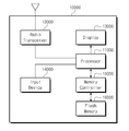
도 10은 본 발명의 실시 예에 따른 메모리 컨트롤러 및 비휘발성 메모리 장치를 포함하는 전자 장치의 블록도를 나타낸다.
도 11은 본 발명의 다른 실시 예에 따른 메모리 컨트롤러 및 비휘발성 메모리 장치를 포함하는 전자 장치의 블록도를 나타낸다.
도 12는 본 발명의 또 다른 실시 예에 따른 비휘발성 메모리 장치를 포함하는 전자 장치의 블록도를 나타낸다.
도 13은 본 발명의 또 다른 실시 예에 따른 메모리 컨트롤러 및 비휘발성 메모리 장치를 포함하는 전자 장치의 블록도를 나타낸다.
도 14는 본 발명의 또 다른 실시 예에 따른 메모리 컨트롤러 및 비휘발성 메모리 장치를 포함하는 전자 장치의 블록도를 나타낸다.
도 15는 도 14에 도시된 전자 장치를 포함하는 데이터 처리 시스템의 블록도를 나타낸다.BRIEF DESCRIPTION OF THE DRAWINGS In order to better understand the drawings cited in the detailed description of the invention, a brief description of each drawing is provided.
1 is a block diagram illustrating a flash memory system according to an exemplary embodiment of the present invention.
FIG. 2 is a block diagram illustrating the memory controller shown in FIG. 1.
3 is a block diagram exemplarily illustrating the flash memory device illustrated in FIG. 1.
4 is a perspective view illustrating an embodiment of one of the memory blocks BLK1 to BLKz of FIG. 3.
FIG. 5 is a cross-sectional view taken along line II ′ of the memory block BLKi of FIG. 4.
FIG. 6 is a diagram illustrating an example of a defect of a NAND string through a cross-sectional view of the memory block illustrated in FIG. 5.
FIG. 7 is an enlarged view of a portion B of FIG. 6.
FIG. 8 is an equivalent circuit diagram of the memory block BLKi shown in FIG. 4.
9 is a flowchart illustrating a method of operating a flash memory system according to an exemplary embodiment of the present invention.
10 is a block diagram of an electronic device including a memory controller and a nonvolatile memory device according to an embodiment of the present disclosure.
11 is a block diagram of an electronic device including a memory controller and a nonvolatile memory device according to another exemplary embodiment of the present disclosure.
12 is a block diagram of an electronic device including a nonvolatile memory device according to another embodiment of the present invention.
13 is a block diagram of an electronic device including a memory controller and a nonvolatile memory device according to another exemplary embodiment of the present disclosure.
14 is a block diagram of an electronic device including a memory controller and a nonvolatile memory device according to another exemplary embodiment of the present disclosure.
FIG. 15 illustrates a block diagram of a data processing system including the electronic device shown in FIG. 14.
본 명세서 또는 출원에 개시되어 있는 본 발명의 개념에 따른 실시 예들에 대해서 특정한 구조적 내지 기능적 설명들은 단지 본 발명의 개념에 따른 실시 예를 설명하기 위한 목적으로 예시된 것으로, 본 발명의 개념에 따른 실시 예들은 다양한 형태로 실시될 수 있으며 본 명세서 또는 출원에 설명된 실시 예들에 한정되는 것으로 해석되어서는 아니 된다.
본 발명의 개념에 따른 실시 예는 다양한 변경을 가할 수 있고 여러 가지 형태를 가질 수 있으므로 특정 실시 예들을 도면에 예시하고 본 명세서 또는 출원에 상세하게 설명하고자 한다. 그러나 이는 본 발명의 개념에 따른 실시 예를 특정한 개시 형태에 대해 한정하려는 것이 아니며, 본 발명의 사상 및 기술 범위에 포함되는 모든 변경, 균등물 내지 대체물을 포함하는 것으로 이해되어야 한다.
제1 및/또는 제2 등의 용어는 다양한 구성 요소들을 설명하는데 사용될 수 있지만, 상기 구성 요소들은 상기 용어들에 의해 한정되어서는 안된다. 상기 용어들은 하나의 구성 요소를 다른 구성 요소로부터 구별하는 목적으로만, 예컨대 본 발명의 개념에 따른 권리 범위로부터 이탈되지 않은 채, 제1 구성요소는 제2 구성요소로 명명될 수 있고, 유사하게 제2 구성요소는 제1 구성요소로도 명명될 수 있다.
어떤 구성요소가 다른 구성요소에 "연결되어" 있다거나 "접속되어" 있다고 언급된 때에는, 그 다른 구성요소에 직접적으로 연결되어 있거나 또는 접속되어 있을 수도 있지만, 중간에 다른 구성요소가 존재할 수도 있다고 이해되어야 할 것이다. 반면에, 어떤 구성요소가 다른 구성요소에 "직접 연결되어" 있다거나 "직접 접속되어" 있다고 언급된 때에는, 중간에 다른 구성요소가 존재하지 않는 것으로 이해되어야 할 것이다. 구성요소들 간의 관계를 설명하는 다른 표현들, 즉 "~사이에"와 "바로 ~사이에" 또는 "~에 이웃하는"과 "~에 직접 이웃하는" 등도 마찬가지로 해석되어야 한다.
본 명세서에서 사용한 용어는 단지 특정한 실시예를 설명하기 위해 사용된 것으로, 본 발명을 한정하려는 의도가 아니다. 단수의 표현은 문맥상 명백하게 다르게 뜻하지 않는 한, 복수의 표현을 포함한다. 본 명세서에서, "포함하다" 또는 "가지다" 등의 용어는 설시된 특징, 숫자, 단계, 동작, 구성요소, 부분품 또는 이들을 조합한 것이 존재함을 지정하려는 것이지, 하나 또는 그 이상의 다른 특징들이나 숫자, 단계, 동작, 구성요소, 부분품 또는 이들을 조합한 것들의 존재 또는 부가 가능성을 미리 배제하지 않는 것으로 이해되어야 한다.
다르게 정의되지 않는 한, 기술적이거나 과학적인 용어를 포함해서 여기서 사용되는 모든 용어들은 본 발명이 속하는 기술 분야에서 통상의 지식을 가진 자에 의해 일반적으로 이해되는 것과 동일한 의미를 갖는다. 일반적으로 사용되는 사전에 정의되어 있는 것과 같은 용어들은 관련 기술의 문맥상 가지는 의미와 일치하는 의미를 갖는 것으로 해석되어야 하며, 본 명세서에서 명백하게 정의하지 않는 한, 이상적이거나 과도하게 형식적인 의미로 해석되지 않는다.
이하, 첨부한 도면을 참조하여 본 발명의 바람직한 실시예를 설명함으로써, 본 발명을 상세히 설명한다.
도 1은 본 발명의 실시 예에 따른 플래시 메모리 시스템을 보여주는 블록도이다. 도 1을 참조하면, 플래시 메모리 시스템(1000)은 플래시 메모리 장치(1100) 및 메모리 컨트롤러(1200)를 포함한다. 도 1에 도시된 플래시 메모리 시스템(1000)에는 메모리 카드, USB 메모리, SSD 등과 같은 플래시 메모리 장치를 기반으로 하는 데이터 저장 매체가 모두 포함될 수 있다.
플래시 메모리 장치(1100)는 메모리 컨트롤러(1200)의 제어에 따라 소거, 쓰기 또는 읽기 동작 등을 수행할 수 있다. 이를 위해 플래시 메모리 장치(1100)는 입출력 라인을 통해 커맨드(CMD), 어드레스(ADDR), 그리고 데이터(DATA)를 입력받는다. 또한, 플래시 메모리 장치(1100)는 전원 라인을 통해 전원(PWR)을 입력받고, 제어 라인을 통해 제어 신호(CTRL)를 입력받는다. 제어 신호(CTRL)에는 커맨드 래치 인에이블(CLE), 어드레스 래치 인에이블(ALE), 칩 인에이블(nCE), 쓰기 인에이블(nWE), 읽기 인에이블(nRE) 등이 포함될 수 있다.
도 2는 도 1에서 도시한 메모리 컨트롤러를 설명하기 위한 블록도이다. 도 2를 참조하면, 메모리 컨트롤러(1200)는 호스트 인터페이스(1201), 플래시 인터페이스(1202), 마이크로프로세서(microprocessor, 1205), 버퍼 메모리(buffer memory; 1204), 레지스터(register; 1203), 그리고 ECC 엔진(1206)을 포함한다. 메모리 컨트롤러(1200)의 각 구성요소(1201~1206)는 버스를 통하여 서로 전기적으로 연결될 수 있다.
호스트 인터페이스(1201)는 호스트와 데이터를 주고 받는데 사용되며, 플래시 인터페이스(1202)는 플래시 메모리 장치(1100)와 데이터를 주고 받는데 사용된다. 플래시 메모리 인터페이스(1202)는 플래시 메모리 장치(1100)의 I/O 패드와 연결되어 있으며, 데이터를 주고 받을 수 있다. 또한, 플래시 메모리 인터페이스(1202)는 플래시 메모리 장치(1100)에 적합한 명령어를 형성하고 I/O 패드를 통해 적합한 명령어를 제공할 수 있다.
마이크로프로세서(1205)는 컨트롤러(1200)를 포함한 플래시 메모리 시스템(1000)의 동작을 전반적으로 제어하고, 플래시 메모리 장치(1100)의 쓰기, 읽기, 또는 소거 동작 등을 제어한다. 플래시 메모리 시스템(1000)에 전원이 인가되면, 마이크로프로세서(1205)는 플래시 메모리 시스템(1000)의 동작을 위한 펌웨어(firmware)를 램(1204) 상에서 구동시킴으로써 플래시 메모리 시스템(1000)의 전반적인 동작을 제어할 수 있다. 마이크로프로세서(1205)의 제어 또는 개입이란, 마이크로프로세서(1205)의 직접적 제어뿐만 아니라, 마이크로프로세서(1205)에 의해서 구동되는 소프트웨어인 펌웨어의 간섭도 포함할 수 있다.
버퍼 메모리(1204)는 플래시 메모리 장치(1100)에 프로그램될 데이터나 호스트로 제공할 데이터를 임시로 저장할 수 있다. 다시 말해서, 버퍼 메모리(1204)는 호스트로부터 입력되는 최초 명령어, 데이터, 각종 변수들 또는 플래시 메모리 장치(1100)로부터 출력되는 데이터들을 저장할 수 있다. 즉, 버퍼 메모리(1204)는 플래시 메모리 장치(1100)로 입력되고 출력되는 데이터, 각종 파라미터 및 변수들을 저장할 수 있다.
또한, 버퍼 메모리(1204)는 플래시 변환 레이어(Flash Translation Layer; FTL)와 같은 펌웨어를 구동하는 데 사용될 수도 있다. 플래시 변환 레이어(FTL)는 마이크로프로세서(1205)에 의해 운용된다. 버퍼 메모리(1204)는 DRAM, SRAM 등과 같은 휘발성 메모리 또는 PRAM, MRAM, Flash memory 등과 같은 비휘발성 메모리로 구현될 수 있다.
ECC 엔진(1206)은 에러 비트를 검출하고 에러 비트 정정을 수행한다. 그러나 ECC 엔진(1206)의 정정 비트 에러 수는 제한되어 있다. ECC 엔진(1206)은 검출된 비트 에러 수가 정정 용량 내이면 비트 에러를 정정할 수 있지만, 정정 용량 밖이면 정정할 수 없다.
계속해서 도 2를 참조하면, ECC엔진(1206)은 ECC 인코더(1207) 및 ECC 디코더(1208)(1208)를 포함한다. ECC 인코더(1207) 플래시 메모리 장치(1100)로 전송되는 데이터를 이용하여, 에러 정정 코드(ECC; Error Correction Code)의 패러티 비트(parity bits)를 생성한다. 페러티 비트(parity bits)는 메인 데이터와 함께 플래시 메모리 장치(1100)에 저장된다. 메인 데이터는 플래시 메모리 장치(1100)의 메인 영역(main area)에 저장되고, 페러티 비트(parity bits)는 스페어 영역(spare area)에 저장된다.
ECC 디코더(1208) 는 출력된 데이터에 대하여 에러 정정 디코딩을 수행하고 수행 결과에 따라 에러 정정 디코딩의 성공 여부를 판단하고, 상기 판단 결과에 따라 지시 신호를 출력한다. 읽은 데이터는 ECC 디코더(1208)로 전송되고, ECC 디코더(1208)는 패리티(parity) 비트를 사용하여 데이터의 에러 비트를 정정할 수 있다. 에러 비트 개수가 정정 가능한 에러 비트 한계치 이상 발생하면, ECC 디코더(1208)는 에러 비트를 정정할 수 없고, 에러 정정 실패(fail) 신호가 발생한다.
ECC 인코더(1207)와 ECC 디코더(1208)는 LDPC(low density parity check) code, BCH code, turbo code, 읽기-솔로몬 코드(Reed-Solomon code), stuck bit code, convolution code, RSC(recursive systematic code), TCM(trellis-coded modulation), BCM(Block coded modulation) 등의 코디드 모듈레이션(coded modulation)을 사용하여 에러 정정을 할 수 있으며 이에 한정되는 것은 아니다.
도 3은 도 1에 도시된 플래시 메모리 장치를 예시적으로 보여주는 블록도이다. 도 3은 예시적으로 3차원 플래시 메모리 장치를 도시하고 있다. 도 3을 참조하면, 플래시 메모리 장치(1100)는 3차원 셀 어레이(1110), 데이터 입출력 회로(1120), 어드레스 디코더(1130), 그리고 제어 로직(1140)을 포함한다.
3차원 셀 어레이(1110)는 복수의 메모리 블록(BLK1~BLKz)을 포함한다. 각각의 메모리 블록은 3차원 구조 (또는 수직 구조)를 가질 수 있다. 2차원 구조 (또는 수평 구조)를 갖는 메모리 블록에서는, 메모리 셀들이 기판과 수평 방향으로 형성된다. 그러나 3차원 구조를 갖는 메모리 블록에서는, 메모리 셀들이 기판과 수직 방향으로 형성된다. 각각의 메모리 블록은 플래시 메모리(1100)의 소거 단위를 이룬다.
데이터 입출력 회로(1120)는 복수의 비트 라인(BLs)을 통해 3차원 셀 어레이(1110)와 연결된다. 데이터 입출력 회로(1120)는 외부로부터 데이터(DATA)를 입력받거나, 3차원 셀 어레이(1110)로부터 읽은 데이터(DATA)를 외부로 출력한다.
어드레스 디코더(1130)는 복수의 워드 라인(WLs) 및 선택 라인(GSL, SSL)을 통해 3차원 셀 어레이(1110)와 연결된다. 어드레스 디코더(1130)는 어드레스(ADDR)를 입력받고 워드 라인을 선택한다.
제어 로직(1140)은 플래시 메모리(1100)의 프로그램, 읽기, 소거 등의 동작을 제어한다. 예를 들면, 제어 로직(1140)은 프로그램 동작 시에, 어드레스 디코더(1130)를 제어함으로 선택 워드 라인으로 프로그램 전압이 제공되도록 하고, 데이터 입출력 회로(1120)를 제어함으로 데이터가 프로그램 되도록 할 수 있다.
도 4는 도 3의 메모리 블록들(BLK1~BLKz) 중 하나(BLKi)의 실시 예를 보여주는 사시도이다. 도 5는 도 4의 메모리 블록(BLKi)의 선(Ⅰ-Ⅰ')에 따른 단면도이다. 도 4 및 도 5를 참조하면, 메모리 블록(BLKi)은 제 1 내지 제 3 방향들을 따라 신장된 구조물들을 포함한다.
우선, 기판(111)이 제공된다. 예시적으로, 기판(111)은 제 1 타입 불순물로 도핑된 실리콘 물질을 포함할 것이다. 예를 들면, 기판(111)은 p 타입 불순물로 도핑된 실리콘 물질을 포함할 것이다. 예를 들면, 기판(111)은 p 타입 웰(예를 들면, 포켓 p 웰)일 것이다. 이하에서, 기판(111)은 p 타입 실리콘인 것으로 가정한다. 그러나, 기판(111)은 p 타입 실리콘으로 한정되지 않는다.
기판(111) 상에, 제 1 방향을 따라 신장된 복수의 웰들(311~314)이 제공된다. 예를 들면, 복수의 웰들(311~314)은 기판(111)과 상이한 제 2 타입 웰들일 것이다. 예를 들면, 복수의 웰들(311~314)은 n 타입 웰들일 것이다. 이하에서, 제 1 내지 제 4 웰들(311~314)은 n-웰들인 것으로 가정한다. 그러나, 제 1 내지 제 4 웰들(311~314)은 n-웰들인 것으로 한정되지 않는다.
제 1 및 제 2 n-웰들(311, 312) 사이에 대응하는 기판(111) 상의 영역에서, 제 1 방향을 따라 신장되는 복수의 절연 물질들(112)이 제 2 방향을 따라 순차적으로 제공된다. 예를 들면, 복수의 절연 물질들(112) 및 기판(111)은 제 2 방향을 따라 미리 설정된 거리만큼 분리되어 형성된다.
예를 들면, 복수의 절연 물질들(112)은 각각 제 2 방향을 따라 미리 설정된 거리만큼 이격되어 제공될 것이다. 예시적으로, 절연 물질들(112)은 실리콘 산화물(Silicon Oxide)일 것이다.
제 1 및 제 2 n-웰들(311, 312) 사이에 대응하는 기판(111) 상의 영역에서, 제 1 방향을 따라 순차적으로 배치되며 제 2 방향을 따라 절연 물질들(112)을 관통하는 복수의 필라들(113)이 제공된다. 예시적으로, 복수의 필라들(113) 각각은 절연 물질들(112)을 관통하여 기판(111)과 연결될 것이다.
예시적으로, 각 필라(113)는 복수의 물질들로 구성될 것이다. 예를 들면, 각 필라(113)의 표면층(114)은 제 1 타입으로 도핑된 실리콘 물질을 포함할 것이다. 예를 들면, 각 필라(113)의 표면층(114)은 기판(111)과 동일한 타입으로 도핑된 실리콘 물질을 포함하여 채널(channel)을 형성할 수 있다. 이하에서, 각 필라(113)의 표면층(114)은 p-타입 실리콘을 포함하는 것으로 가정한다. 그러나, 각 필라(113)의 표면층(114)은 p-타입 실리콘을 포함하는 것으로 한정되지 않는다.
각 필라(113)의 내부층(115)은 절연 물질로 구성된다. 예를 들면, 각 필라(113)의 내부층(115)은 실리콘 산화물(Silicon Oxide)로 구성될 것이다.
제 1 및 제 2 n-웰들(311, 312) 사이의 영역에서, 절연 물질들(112), 필라들(113), 그리고 기판(111)의 노출된 표면을 따라 절연막(116)이 제공된다. 예시적으로, 절연막(116)의 두께는 절연 물질들(112) 사이의 거리의 1/2 보다 작을 것이다. 즉, 절연 물질들(112) 중 제 1 절연 물질의 하부면에 제공된 절연막(116), 그리고 제 1 절연 물질 하부의 제 2 절연 물질의 상부면에 제공된 절연막(116) 사이에, 절연 물질들(112) 및 절연막(116) 이외의 물질이 배치될 수 있는 영역이 제공될 것이다.
제 1 및 제 2 n-웰들(311, 312) 사이의 영역에서, 절연막(116)의 노출된 표면 상에 도전 물질들(211~21)이 제공된다. 예를 들면, 기판(111)에 인접한 절연 물질(112) 및 기판(111) 사이에 제 1 방향을 따라 신장되는 도전 물질(211)이 제공된다. 더 상세하게는, 기판(111)에 인접한 절연 물질(112)의 하부면의 절연막(116) 및 기판(111) 사이에 제 1 방향으로 신장되는 도전 물질(211)이 제공된다.
절연 물질들(112) 중 특정 절연 물질 상부면의 절연막(116) 및 특정 절연 물질 상부에 배치된 절연 물질의 하부면의 절연막(116) 사이에, 제 1 방향을 따라 신장되는 도전 물질이 제공된다. 예시적으로, 절연 물질들(112) 사이에, 제 1 방향으로 신장되는 복수의 도전 물질들(221~281)이 제공된다. 또한, 절연 물질들(112) 상의 영역에 제 1 방향을 따라 신장되는 도전 물질(291)이 제공된다. 예시적으로, 제 1 방향으로 신장된 도전 물질들(211~291)은 금속 물질일 것이다. 예시적으로, 제 1 방향으로 신장된 도전 물질들(211~291)은 폴리 실리콘 등과 같은 도전 물질들일 것이다.
제 2 및 제 3 n-웰들(312, 313) 사이의 영역에서, 제 1 및 제 2 n-웰들(311, 312) 상의 구조물과 동일한 구조물이 제공될 것이다. 예시적으로, 제 2 및 제 3 n-웰들(312, 313) 사이의 영역에서, 제 1 방향으로 신장되는 복수의 절연 물질들(112), 제 1 방향을 따라 순차적으로 배치되며 제 3 방향을 따라 복수의 절연 물질들(112)을 관통하는 복수의 필라들(113), 복수의 절연 물질들(112) 및 복수의 필라들(113)의 노출된 표면에 제공되는 절연막(116), 그리고 제 1 방향을 따라 신장되는 복수의 도전 물질들(212~292)이 형성된다. 제 3 및 제 4 n-웰들(313, 314) 사이의 영역에서, 제 1 및 제 2 n-웰들(311, 312) 상의 구조물과 동일한 구조물이 제공될 것이다. 예시적으로, 제 3 및 제 4 n-웰들(312, 313) 사이의 영역에서, 제 1 방향으로 신장되는 복수의 절연 물질들(112), 제 1 방향을 따라 순차적으로 배치되며 제 3 방향을 따라 복수의 절연 물질들(112)을 관통하는 복수의 필라들(113), 복수의 절연 물질들(112) 및 복수의 필라들(113)의 노출된 표면에 제공되는 절연막(116), 그리고 제 1 방향을 따라 신장되는 복수의 도전 물질들(213~293)이 제공된다. 게이트들(또는 제어 게이트들)은 제 1 및 제 2 방향으로 신장된 도전 물질들(211~291, 212~292, 213~293)에 대응한다. 즉, 게이트들(또는 제어 게이트들)은 제 1 방향으로 신장되어 워드 라인들, 그리고 적어도 두 개의 선택 라인들(예를 들면, 적어도 하나의 스트링 선택 라인(SSL) 및 적어도 하나의 접지 선택 라인(GSL)을 형성한다.
복수의 필라들(113) 상부에 드레인들(320)이 각각 제공된다. 예시적으로, 드레인들(320)은 제 2 타입으로 도핑된 실리콘 물질들일 것이다. 예를 들면, 드레인들(320)은 n 타입으로 도핑된 실리콘 물질들일 것이다. 이하에서, 드레인들(320)는 n-타입 실리콘을 포함하는 것으로 가정한다. 그러나, 드레인들(320)은 n-타입 실리콘을 포함하는 것으로 한정되지 않는다. 예시적으로, 각 드레인(320)의 폭은 대응하는 필라(113)의 폭 보다 클 수 있다. 예를 들면, 각 드레인(320)은 대응하는 필라(113)의 상부면에 패드 형태로 제공될 수 있다.
드레인들(320) 상에, 제 3 방향으로 신장된 도전 물질들(331~333)이 제공된다. 도전 물질들(331~333)은 제 1 방향을 따라 순차적으로 배치된다. 도전 물질들(331~333) 각각은 대응하는 영역의 드레인들(320)과 연결된다. 예시적으로, 드레인들(320) 및 제 3 방향으로 신장된 도전 물질(333)은 각각 콘택 플러그들(contact plug)을 통해 연결될 수 있다. 도전 물질들(331~333)은 비트 라인을 형성할 수 있다. 예시적으로, 제 3 방향으로 신장된 도전 물질들(331~333)은 금속 물질들일 것이다. 예시적으로, 제 3 방향으로 신장된 도전 물질들(331~333)은 폴리 실리콘 등과 같은 도전 물질들일 것이다.
도 4 및 도 5에서, 각 필라(113)는 절연막(116)의 인접한 영역 및 제 1 방향을 따라 신장되는 복수의 도체 라인들(211~291, 212~292, 213~293) 중 인접한 영역과 함께 스트링을 형성한다. 예를 들면, 각 필라(113)는 절연막(116)의 인접한 영역 및 제 1 방향을 따라 신장되는 복수의 도체 라인들(211~291, 212~292, 213~293) 중 인접한 영역과 함께 낸드 스트링(NS)을 형성한다. 낸드 스트링(NS)은 복수의 트랜지스터 구조들(TS)을 포함한다. 각각의 낸드 스트링은 스트링 선택 트랜지스터(SST), 접지 선택 트랜지스터(GST), 메모리 셀들 및 스트링 선택 트랜지스터, 전지 선택 트랜지스터, 및 메모리 셀들을 전기적으로 연결시켜주는 필라(pillar)를 포함할 수 있다. 드레인(320)은 복수의 필라들(113) 상부에 드레인들(320)이 각각 제공된다. 예를 들면, 드레인(320)은 대응하는 필라(113)의 상부에 패드 형태로 제공될 수 있다. 드레인(320)은 스트링 선택 트렌지스터(SST)와 전기적으로 연결된다. 도전 물질들(331~333), 즉, 비트 라인들은 각각은 대응하는 영역의 드레인들(320)과 연결된다. 앞에서 설명한 바와 같이, 드레인들(320) 및 비트 라인은 각각 콘택 플러그들(contact plug)을 통해 연결될 수 있다.
도 6은 도 5에 도시된 메모리 블록의 낸드 스트링의 결함(defect) 예를 보여주는 도면이다.
도 6의 A 부분을 참조하면, 낸드 스트링은 제조 공정 시에 드레인들(320) 및 비트 라인 사이의 패드(pad) 부분에서 결함이 발생할 수 있다. 그 결과 낸드 스트링의 채널이 형성되지 않을 수 있다.
제조 공정상의 결함으로, 스트링 선택 트랜지스터(SST)와 콘택 플러그(320)는 전기적으로 연결되지 않을 수 있다. 즉, 콘택 플러그(320)의 공정상의 결함으로 인하여, 낸드 스트링은 비트 라인과 전기적으로 연결되지 않을 수 있다. 이때 낸드 스트링의 모든 메모리 셀은, 프로그램된 본래 데이터(original data)와 상관없이, 항상 오프 상태 (off state)가 된다.
도 6의 B 부분을 참조하면, 낸드 스트링은 제조 공정상의 결함으로 인해, 그라운드 선택 트랜지스터와 기판이 전기적으로 연결되지 않을 수도 있다. 이 경우에도 낸드 스트링의 채널이 형성되지 않을 수 있다. 도 7은 도 6의 B 부분을 확대해서 보여주는 도면이다. 도 7을 참조하면, 비휘발성 메모리 장치의 제조 시에, 공정상의 결함으로 그라운드 선택 트랜지스터(212, GST)는 기판 및 필러에 전기적으로 연결되지 않는 구조로 형성될 수 있다. 예를 들면, 필라를 형성하는 과정에서 에칭(etching)의 실패로, 필라가 그라운드 선택 트랜지스터(212, GST)까지 연결되지 않을 수 있다.
도 6의 C 부분을 참조하면, 메모리 셀의 채널 형성 시에, 에칭이나 증착 등의 오류로 인해 불량이 생긴 경우에도 스트링 채널이 형성되지 않을 수 있다. 채널이 형성되지 않은 스트링에 포함된 메모리 셀들은 프로그램 데이터와 상관없이, 읽기 동작 시에 항상 오프 상태로 읽힐 수 있다.
도 8은 도 4에 도시된 메모리 블록(BLKi)의 등가 회로도이다. 도 8을 참조하면, 비트 라인(BL1~BL3)과 공통 소스 라인(CSL) 사이에는 낸드 스트링(NS11~NS33)이 연결되어 있다.
각각의 낸드 스트링(예를 들면, NS11)은 스트링 선택 트랜지스터(SST), 복수의 메모리 셀(MC1~MC8), 그리고 접지 선택 트랜지스터(GST)를 포함한다. 스트링 선택 트랜지스터(SST)는 스트링 선택 라인(String Selection Line; SSL1~SSL3)에 연결되어 있다. 복수의 메모리 셀(MC1~MC8)은 각각 대응하는 워드 라인(WL1~WL8)에 연결되어 있다. 그리고 접지 선택 트랜지스터(GST)는 접지 선택 라인(Ground Selection Line; GSL1~GSL3)에 연결되어 있다. 스트링 선택 트랜지스터(SST)는 비트 라인(BL)에 연결되고, 접지 선택 트랜지스터(GST)는 공통 소스 라인(CSL; Common Source Line)에 연결되어 있다.
계속해서 도 8을 참조하면, 동일 높이의 워드 라인(예를 들면, WL1)은 공통으로 연결되어 제 1 워드 라인을 형성하고, 스트링 선택 라인(SSL1~SSL3)은 분리되어 있다. 제 1 워드 라인(WL1)에 연결되고 낸드 스트링(NS11, NS12, NS13)에 속해 있는 메모리 셀(이하, 페이지라 함)을 프로그램하는 경우에는, 제 1 워드 라인(WL1)과 제 1 스트링 선택 라인(SSL1)이 선택된다.
제 1 워드 라인에는 제 1 패스 전압을 제공하여, 상기 제 1 워드 라인을 읽는다. 제 1 패스 전압은 3차원 플래시 메모리 장치의 미리 정해진 프로그램 상태에 대응되는 문턱 전압보다 높은 전압이다. 플래시 메모리 장치가 프로그램 이전의 상태이면, 제 1 패스 전압은 소거 상태에 대응되는 전압일 수 있다. 예시적으로 제 1 워드 라인은 3차원 적층된 셀 어레이에서 최하단의 워드 라인일 수 있다.
스트링 선택 트랜지스터(SST)가 비트 라인과 전기적으로 연결되지 않은 낸드 스트링은 읽기 동작 시에 항상 오프 상태로 된다. 그라운드 선택 트랜지스터(GST)가 기판과 전기적으로 연결되지 않은 낸드 스트링의 메모리 셀들은 제 1 패스 전압을 제공 시에 항상 오프 상태로 된다. 또한, 특정 메모리 셀이 전기적으로 채널이 형성되지 않은 낸드 스트링은 모두 오프 상태(off state)로 된다.
본 발명은 3차원 플래시 메모리 장치에서 위에서 설명한 공정상의 결함으로 인해, 채널이 형성되지 않은 경우에 발생하는 에러 비트를 정정하기 위한 방법에 관한 것이다. 에러 예측에 있어서, 공정상의 이유로 채널이 물리적으로 단락된 것은 메모리 셀의 특성으로 인한 것과 다를 수 있다. 즉, 메모리 셀의 특성으로 인한 에러는 예측이 쉽지 않으나, 공정상의 이유로 인한 채널의 단락은 예측이 매우 쉽다.
채널 단락으로 인한 에러는 단순한 읽기 동작을 통해 쉽게 알 수 있다. 즉, 모든 메모리 셀이 소거 상태가 되도록 한 다음에, 읽기 동작을 수행한 결과 오프 상태(off state)인 데이터가 나오면 채널 단락이라고 예측할 수 있다.
다시 도 3을 참조하면, 제어 로직(1140)은 제 1 워드 라인에 제 1 패스 전압을 인가하고, 제 1 워드 라인에 연결된 메모리 셀들 중에 오프 상태인 메모리 셀에 대응되는 낸드 스트링의 주소 정보를 확인하고, 그 정보를 메모리 셀 어레이에 저장할 수 있다. 또는 제어 로직(1140)은 낸드 스트링 주소 정보를 메모리 컨트롤러(1200)로 제공할 수 있다. 낸드 스트링 주소 정보는 비트 라인 주소 및 블록 주소를 포함하며, 또는 페이지 주소도 일부 포함할 수 있다.
도 9는 본 발명의 실시 예에 따른 플래시 메모리 시스템의 동작 방법을 보여주는 순서도이다.
S110 단계에서, 오프 상태인 메모리 셀에 대응되는 낸드 스트링의 주소 정보를 확인한다. 도 2 및 도 3을 참조하면, 메모리 컨트롤러(1200)는 기판과 수직 방향으로 배열되는 복수의 셀 스트링을 갖는 플래시 메모리 장치(1100)의 동작을 제어한다. 메모리 컨트롤러(1200)는 플래시 메모리 장치의 제 1 워드 라인에 제 1 워드 라인 전압을 제공하고, 제 1 워드 라인에 포함된 메모리 셀들을 읽고, 오프 상태인 메모리 셀들에 대응되는 낸드 스트링 주소 정보를 서치하도록 제어할 수 있다.
제 1 워드 라인 전압이란 미리 정해진 프로그램 상태에 대응되는 문턱 전압보다 큰 전압이 될 수 있다. 오프 상태 셀들은 공정상의 결함으로 전기적으로 채널이 형성되지 않은 낸드 스트링에 포함되는 셀들이다. 구체적으로, 오프 상태 셀들은 예를 들면, 메모리 셀의 결함으로 채널을 형성하지 못한 경우, 접지 선택 트랜지스터가 기판에 전기적으로 연결되지 않는 경우, 스트링 선택 트랜지스터가 비트 라인에 전기적으로 연결이 되지 않은 경우에 발생할 수 있다.
S120 단계에서, 메모리 컨트롤러(1200)는 서치된 낸드 스트링 주소 정보를 참조하여, 낸드 스트링 주소 정보에 대응되는 원본 데이터를 소정의 프로그램 상태로 맵핑하고, 맵핑 정보를 플래시 메모리 장치(1100) 또는 레지스터(1203)에 저장할 수 있다. 소정의 프로그램 상태는 플래시 메모리 장치(1100)의 미리 정해진 최상위 프로그램 상태보다 더 높은 문턱 전압을 가지는 상태일 수 있다.
S130 단계에서, 메모리 컨트롤러(1200) 내의 ECC 디코더(1208)는 맵핑된 데이터 및 서치된 주소 정보에 대응되지 않은 원본 데이터를 인코딩하고, 인코딩된 데이터를 플래시 메모리 장치(1100)로 제공한다. 플래시 메모리 장치(1100)는 제공받은 데이터를 프로그램할 수 있다.
본 발명의 실시 예에 따른 3차원 플래시 메모리 장치는 공정상의 이유로 채널이 단락된 경우에 비트 에러를 쉽게 예측할 수 있고 효율적으로 비트 에러율을 개선할 수 있다.
도 10은 본 발명의 실시 예에 따른 메모리 컨트롤러(15000) 및 비휘발성 메모리 장치(16000)를 포함하는 전자 장치(10000)의 블록도를 나타낸다.
도 10을 참조하면, 이동 전화기(cellular phone), 스마트 폰(smart phone), 또는 태블릿(tablet) PC와 같은 전자 장치(10000)는 플래시 메모리 장치로 구현될 수 있는 비휘발성 메모리 장치(16000)와, 비휘발성 메모리 장치(16000)의 동작을 제어할 수 있는 메모리 컨트롤러(15000)를 포함할 수 있다.
메모리 컨트롤러(15000)는 전자 장치의 전반적인 동작을 제어하는 프로세서(11000)에 의하여 제어된다.
비휘발성 메모리 장치(16000)에 저장된 데이터는 프로세서(11000)의 제어에 따라 동작하는 메모리 컨트롤러(15000)의 제어에 따라 디스플레이(13000)를 통하여 디스플레이될 수 있다.
무선 송수신기(12000)는 안테나(ANT)를 통하여 무선 신호를 주거나 받을 수 있다. 예컨대, 무선 송수신기(12000)는 안테나(ANT)를 통하여 수신된 무선 신호를 프로세서(11000)가 처리할 수 있는 신호로 변환할 수 있다. 따라서 프로세서(11000)는 무선 송수신기(12000)로부터 출력된 신호를 처리하고, 처리된 신호를 메모리 컨트롤러(15000)를 통하여 비휘발성 메모리 장치(16000)에 저장하거나 또는 디스플레이(13000)를 통하여 디스플레이할 수 있다.
무선 송수신기(12000)는 프로세서(11000)로부터 출력된 신호를 무선 신호로 변환하고, 변환된 무선 신호를 안테나(ANT)를 통하여 외부로 출력할 수 있다.
입력 장치(14000)는 프로세서(11000)의 동작을 제어하기 위한 제어 신호 또는 프로세서(11000)에 의하여 처리될 데이터를 입력할 수 있는 장치로서, 터치 패드 (touch pad)와 컴퓨터 마우스(computer mouse)와 같은 포인팅 장치(pointing device), 키패드(keypad), 또는 키보드로 구현될 수 있다.
프로세서(11000)는 비휘발성 메모리 장치(16000)로부터 출력된 데이터, 무선 송수신기(12000)로부터 출력된 무선 신호, 또는 입력 장치(14000)로부터 출력된 데이터가 디스플레이(13000)를 통하여 디스플레이될 수 있도록 디스플레이(13000)를 제어할 수 있다.
도 11은 본 발명의 다른 실시 예에 따른 메모리 컨트롤러(24000)및 비휘발성 메모리 장치(25000)를 포함하는 전자 장치(20000)의 블록도를 나타낸다.
도 11을 참조하면, PC(personal computer), 태블릿 컴퓨터(tablet computer), 넷-북(net-book), e-리더(e-reader), PDA(personal digital assistant), PMP(portable multimedia player), MP3 플레이어, 또는 MP4 플레이어와 같은 데이터 처리 장치로 구현될 수 있는 전자 장치(20000)는 플래시 메모리 장치와 같은 비휘발성 메모리 장치(25000)와, 비휘발성 메모리 장치(25000)의 동작을 제어할 수 있는 메모리 컨트롤러(24000)를 포함한다.
비휘발성 메모리 장치(16000)는 도 1 및 도 11에서 도시한 비휘발성 메모리 장치를 의미할 수 있다. 비휘발성 메모리 장치(16000)는 랜덤 데이터를 저장 할 수 있다.
전자 장치(20000)는 전자 장치(20000)의 전반적인 동작을 제어하기 위한 프로세서(21000)를 포함할 수 있다. 메모리 컨트롤러(24000)는 프로세서(21000)에 의하여 제어된다.
프로세서(21000)는 입력 장치(22000)에 의하여 발생한 입력 신호에 따라 비휘발성 메모리 장치에 저장된 데이터를 디스플레이를 통하여 디스플레이할 수 있다. 예컨대, 입력 장치(22000)는 터치 패드 또는 컴퓨터 마우스와 같은 포인팅 장치, 키패드, 또는 키보드로 구현될 수 있다.
도 12는 본 발명의 또 다른 실시 예에 따른 비휘발성 메모리 장치(34000)를 포함하는 전자 장치(30000)의 블록도를 나타낸다.
도 12를 참조하면, 전자 장치(30000)는 카드 인터페이스(31000), 메모리 컨트롤러(32000), 및 비휘발성 메모리 장치(34000), 예컨대 플래시 메모리 장치를 포함한다.
전자 장치(30000)는 카드 인터페이스(31000)를 통하여 호스트(HOST)와 데이터를 주거나 받을 수 있다. 실시 예에 따라, 카드 인터페이스(31000)는 SD(secure digital) 카드 인터페이스 또는 MMC(multi-media card) 인터페이스일 수 있으나 이에 한정되는 것은 아니다. 카드 인터페이스(31000)는 전자 장치(30000)와 통신할 수 있는 호스트(HOST)의 통신 프로토콜에 따라 호스트(HOST)와 메모리 컨트롤러(32000) 사이에서 데이터 교환을 인터페이스할 수 있다.
메모리 컨트롤러(32000)는 전자 장치(30000)의 전반적인 동작을 제어하며, 카드 인터페이스(31000)와 비휘발성 메모리 장치(34000) 사이에서 데이터의 교환을 제어할 수 있다. 또한 메모리 컨트롤러(32000)의 버퍼 메모리(325)는 카드 인터페이스(31000)와 비휘발성 메모리 장치(34000) 사이에서 주고받는 데이터를 버퍼링할 수 있다.
메모리 컨트롤러(32000)는 데이터 버스(DATA) 및 어드레스 버스(ADDRESS)를 통하여 카드 인터페이스(31000)와 비휘발성 메모리 장치(34000)와 접속된다. 실시 예에 따라 메모리 컨트롤러(32000)는 카드 인터페이스(31000)로부터 읽기 또는 라이트하고자 하는 데이터의 어드레스를 어드레스 버스(ADDRESS)를 통하여 수신하고 이를 비휘발성 메모리 장치(34000)로 전송한다.
또한, 메모리 컨트롤러(32000)는 카드 인터페이스(31000) 또는 비휘발성 메모리 장치(34000) 각각에 접속된 데이터 버스(DATA)를 통하여 읽기 또는 라이트하고자 하는 데이터를 수신하거나 전송한다. 비휘발성 메모리 장치(16000)는 도 1 및 도 2에서 도시한 플래시 메모리 장치를 의미할 수 있다. 비휘발성 메모리 장치(16000)는 랜덤 데이터를 저장할 수 있다.
도 12의 전자 장치(30000)가 PC, 태블릿 PC, 디지털 카메라, 디지털 오디오 플레이어, 이동 전화기, 콘솔 비디오 게임 하드웨어, 또는 디지털 셋-탑 박스와 같은 호스트(HOST)에 접속될 때, 호스트(HOST)는 카드 인터페이스(31000)와 메모리 컨트롤러(32000)를 통하여 비휘발성 메모리 장치(34000)에 저장된 데이터를 주거나 받을 수 있다.
도 13은 본 발명의 또 다른 실시 예에 따른 메모리 컨트롤러 및 비휘발성 메모리 장치를 포함하는 전자 장치의 블록도를 나타낸다.
도 13을 참조하면, 전자 장치(40000)는 플래시 메모리 장치와 같은 비휘발성 메모리 장치(45000), 비휘발성 메모리 장치(45000)의 데이터 처리 동작을 제어하기 위한 메모리 컨트롤러(44000), 및 전자 장치(40000)의 전반적인 동작을 제어할 수 있는 이미지 센서(41000)를 포함한다.
전자 장치(40000)의 이미지 센서(42000)는 광학 신호를 디지털 신호로 변환하고, 변환된 디지털 신호는 이미지 센서(41000)의 제어하에 비휘발성 메모리 장치(45000)에 저장되거나 또는 디스플레이(43000)를 통하여 디스플레이된다. 또한, 비휘발성 메모리 장치(45000)에 저장된 디지털 신호는 이미지 센서(41000)의 제어하에 디스플레이(43000)를 통하여 디스플레이된다.
도 14는 본 발명의 또 다른 실시 예에 따른 메모리 컨트롤러(61000) 및 비휘발성 메모리 장치(62000A, 62000B, 62000C)를 포함하는 전자 장치(60000)의 블록도를 나타낸다. 도 14를 참조하면, 전자 장치(60000)는 SSD(solid state drive)와 같은 데이터 저장 장치로 구현될 수 있다.
전자 장치(60000)는 다수개의 비휘발성 메모리 장치들(62000A, 62000B, 62000C)과, 다수개의 비휘발성 메모리 장치들(62000A, 62000B, 62000C) 각각의 데이터 처리 동작을 제어할 수 있는 메모리 컨트롤러(61000)를 포함할 수 있다.
전자 장치(60000)는 메모리 시스템 또는 메모리 모듈로 구현될 수 있다.
비휘발성 메모리 장치(16000)는 도 1 및 도 2에서 도시한 플래시 메모리 장치를 의미할 수 있다. 비휘발성 메모리 장치(16000)는 랜덤 데이터를 저장할 수 있다. 실시 예에 따라 메모리 컨트롤러(61000)는 전자 장치(60000)의 내부 또는 외부에 구현될 수 있다.
도 15는 도 14에 도시된 전자 장치를 포함하는 데이터 처리 시스템의 블록도를 나타낸다. 도 14와 도 15를 참조하면, RAID(redundant array of independent disks) 시스템으로 구현될 수 있는 데이터 저장 장치(70000)는 RAID 컨트롤러(71000)와, 다수개의 메모리 시스템들(72000A, 72000B ~72000N; N는 자연수)을 포함할 수 있다.
다수개의 메모리 시스템들(72000A, 72000B ~72000N) 각각은 도 13에 도시된 전자 장치 (700)일 수 있다. 다수개의 메모리 시스템들(72000A, 72999B ~72000N)은 RAID 어레이를 구성할 수 있다. 데이터 저장 장치(70000)는 PC(personal computer) 또는 SSD로 구현될 수 있다.
프로그램 동작 동안, RAID 컨트롤러(71000)는 호스트로부터 출력된 프로그램 데이터를 다수개의 RAID 레벨들 중에서 호스트로부터 출력된 RAID 레벨 정보에 기초하여 선택된 어느 하나의 RAID 레벨에 따라 다수개의 메모리 시스템들(72000A, 72000B ~72000N) 중에서 어느 하나의 메모리 시스템으로 출력할 수 있다.
또한, 읽기 동작 동안, RAID 컨트롤러(71000)는 다수개의 RAID 레벨들 중에서 호스트로부터 출력된 RAID 레벨 정보에 기초하여 선택된 어느 하나의 RAID 레벨에 따라서 다수개의 메모리 시스템 중(72000A, 72000B ~72000N)에서 어느 하나의 메모리 시스템으로부터 읽은 데이터를 호스트로 전송할 수 있다.
다수개의 메모리 시스템 각각의(72000A, 72000B ~72000N) 메모리 컨트롤러는 도 1에서 도시한 씨드 컨트롤러(1260)을 포함한 메모리 컨트롤러를 의미할 수 있다. 메모리 컨트롤러(44000)는 제 1 파라미터를 사용하여 제 1 시클릭 시프트를 수행하기 위한 제 1 레지스터 블록, 제 2 파라미터를 사용하여 제 2 시클릭 시프트를 수행하기 위한 제 2 레지스터 블록, 및 제 1 및 제 2 레지스터 블록에서 수행된 시클릭 시프트 결과를 사용하여 씨드를 형성하는 씨드 생성 블록을 포함하고, 생성된 씨드를 사용하여 오리지널 데이터를 랜덤데이터로 랜덤화 할 수 있다.
본 발명은 도면에 도시된 일 실시 예를 참고로 설명되었으나 이는 예시적인 것에 불과하며, 본 기술 분야의 통상의 지식을 가진 자라면 이로부터 다양한 변형 및 균등한 타 실시 예가 가능하다는 점을 이해할 것이다. 따라서, 본 발명의 진정한 기술적 보호 범위는 첨부된 등록청구범위의 기술적 사상에 의해 정해져야 할 것이다.
한편, 본 발명의 상세한 설명에서는 구체적인 실시 예에 관하여 설명하였으나, 본 발명의 범위에서 벗어나지 않는 한도 내에서 여러 가지 변형이 가능함은 물론이다. 그러므로 본 발명의 범위는 상술한 실시예에 국한되어 정해져서는 안되며 후술하는 특허청구범위뿐만 아니라 이 발명의 특허청구범위와 균등한 것들에 의해 정해져야 한다.
본 발명은 도면에 도시된 일 실시 예를 참고로 설명되었으나 이는 예시적인 것에 불과하며, 본 기술 분야의 통상의 지식을 가진 자라면 이로부터 다양한 변형 및 균등한 타 실시 예가 가능하다는 점을 이해할 것이다. 따라서, 본 발명의 진정한 기술적 보호 범위는 첨부된 등록청구범위의 기술적 사상에 의해 정해져야 할 것이다.
한편, 본 발명의 상세한 설명에서는 구체적인 실시 예에 관하여 설명하였으나, 본 발명의 범위에서 벗어나지 않는 한도 내에서 여러 가지 변형이 가능함은 물론이다. 그러므로 본 발명의 범위는 상술한 실시예에 국한되어 정해져서는 안되며 후술하는 특허청구범위뿐만 아니라 이 발명의 특허청구범위와 균등한 것들에 의해 정해져야 한다.Specific structural to functional descriptions of embodiments according to the inventive concept disclosed in the specification or the application are only illustrated for the purpose of describing embodiments according to the inventive concept, and according to the inventive concept. The examples may be embodied in various forms and should not be construed as limited to the embodiments set forth herein or in the application.
Embodiments according to the concept of the present invention may be variously modified and may have various forms, and specific embodiments will be illustrated in the drawings and described in detail in the present specification or application. However, this is not intended to limit the embodiments in accordance with the concept of the present invention to a particular disclosed form, it should be understood to include all changes, equivalents, and substitutes included in the spirit and scope of the present invention.
Terms such as first and / or second may be used to describe various components, but the components should not be limited by the terms. The terms are used only for the purpose of distinguishing one component from another, for example, without departing from the scope of rights in accordance with the inventive concept, and the first component may be called a second component and similarly The second component may also be referred to as the first component.
When a component is referred to as being "connected" or "connected" to another component, it may be directly connected to or connected to that other component, but it may be understood that other components may be present in between. Should be. On the other hand, when a component is said to be "directly connected" or "directly connected" to another component, it should be understood that there is no other component in between. Other expressions describing the relationship between components, such as "between" and "immediately between," or "neighboring to," and "directly neighboring to" should be interpreted as well.
The terminology used herein is for the purpose of describing particular embodiments only and is not intended to be limiting of the invention. Singular expressions include plural expressions unless the context clearly indicates otherwise. As used herein, the terms "comprise" or "having" are intended to indicate that there is a feature, number, step, action, component, part, or combination thereof that is described, and that one or more other features or numbers are present. It should be understood that it does not exclude in advance the possibility of the presence or addition of steps, actions, components, parts or combinations thereof.
Unless defined otherwise, all terms used herein, including technical or scientific terms, have the same meaning as commonly understood by one of ordinary skill in the art. Terms such as those defined in the commonly used dictionaries should be construed as having meanings consistent with the meanings in the context of the related art, and are not construed in ideal or excessively formal meanings unless expressly defined herein. Do not.
Hereinafter, exemplary embodiments of the present invention will be described in detail with reference to the accompanying drawings.
1 is a block diagram illustrating a flash memory system according to an exemplary embodiment of the present invention. Referring to FIG. 1, the
The
FIG. 2 is a block diagram illustrating the memory controller shown in FIG. 1. Referring to FIG. 2, the
The
The
The
The
The
With continued reference to FIG. 2, the
The
The
3 is a block diagram exemplarily illustrating the flash memory device illustrated in FIG. 1. 3 exemplarily illustrates a three-dimensional flash memory device. Referring to FIG. 3, the
The
The data input /
The
The
4 is a perspective view illustrating an embodiment of one of the memory blocks BLK1 to BLKz of FIG. 3. FIG. 5 is a cross-sectional view taken along line II ′ of the memory block BLKi of FIG. 4. 4 and 5, the memory block BLKi includes structures extending along first to third directions.
First, the
On the
In the region on the
For example, the plurality of insulating
In a region on the
For example, each
The
In the region between the first and second n-
In the region between the first and second n-
A conductive material extending along the first direction is provided between the insulating
In the region between the second and third n-
On the
4 and 5, each
FIG. 6 is a diagram illustrating a defect example of a NAND string of a memory block illustrated in FIG. 5.
Referring to part A of FIG. 6, the NAND string may have a defect in a pad portion between the
As a defect in the manufacturing process, the string select transistor SST and the
Referring to part B of FIG. 6, the NAND string may not be electrically connected to the ground select transistor and the substrate due to a defect in the manufacturing process. Even in this case, a channel of the NAND string may not be formed. FIG. 7 is an enlarged view of a portion B of FIG. 6. Referring to FIG. 7, in manufacturing a nonvolatile memory device, the ground
Referring to part C of FIG. 6, when a channel of a memory cell is formed, a string channel may not be formed even when a defect occurs due to an error such as etching or deposition. Memory cells included in a string in which a channel is not formed may be always read in an off state during a read operation, regardless of program data.
FIG. 8 is an equivalent circuit diagram of the memory block BLKi shown in FIG. 4. Referring to FIG. 8, NAND strings NS11 to NS33 are connected between the bit lines BL1 to BL3 and the common source line CSL.
Each NAND string (eg, NS11) includes a string select transistor SST, a plurality of memory cells MC1 to MC8, and a ground select transistor GST. The string selection transistor SST is connected to a string selection line SSL1 to SSL3. The plurality of memory cells MC1 to MC8 are connected to corresponding word lines WL1 to WL8, respectively. The ground selection transistor GST is connected to ground selection lines GSL1 to GSL3. The string select transistor SST is connected to the bit line BL, and the ground select transistor GST is connected to the common source line CSL.
8, word lines (eg, WL1) having the same height are commonly connected to form a first word line, and string select lines SSL1 to SSL3 are separated. When programming a memory cell (hereinafter, referred to as a page) connected to the first word line WL1 and belonging to the NAND strings NS11, NS12, and NS13, the first word line WL1 and the first string select line. (SSL1) is selected.
The first word line is provided with a first pass voltage to read the first word line. The first pass voltage is a voltage higher than a threshold voltage corresponding to a predetermined program state of the 3D flash memory device. When the flash memory device is in a state before the program, the first pass voltage may be a voltage corresponding to the erase state. In exemplary embodiments, the first word line may be a lowermost word line in a three-dimensional stacked cell array.
A NAND string in which the string select transistor SST is not electrically connected to the bit line is always turned off in a read operation. NAND string memory cells whose ground select transistor GST is not electrically connected to the substrate are always in an OFF state when providing a first pass voltage. In addition, all of the NAND strings in which a specific memory cell is not electrically channeled are turned off.
The present invention relates to a method for correcting an error bit that occurs when a channel is not formed due to the process defect described above in a three-dimensional flash memory device. In error prediction, the physical short circuit of the channel for process reasons may differ from that due to the characteristics of the memory cell. That is, the error due to the characteristics of the memory cell is not easy to predict, but the short circuit of the channel due to process reasons is very easy to predict.
Errors due to channel short circuits can be easily identified by simple read operations. That is, after all memory cells are in an erased state, when a read operation results in data that is in an off state, a short circuit may be predicted as a channel short circuit.
Referring back to FIG. 3, the
9 is a flowchart illustrating a method of operating a flash memory system according to an exemplary embodiment of the present invention.
In step S110, the address information of the NAND string corresponding to the off-state memory cell is checked. 2 and 3, the
The first word line voltage may be a voltage larger than a threshold voltage corresponding to a predetermined program state. Off-state cells are cells included in a NAND string that are not electrically channeled due to a process defect. Specifically, the off-state cells, for example, fail to form a channel due to a defect in the memory cell, the ground select transistor is not electrically connected to the substrate, or the string select transistor is not electrically connected to the bit line. May occur.
In operation S120, the
In operation S130, the
The 3D flash memory device according to an exemplary embodiment of the present invention can easily predict a bit error when a channel is shorted for processing reasons and can efficiently improve a bit error rate.
10 is a block diagram of an
Referring to FIG. 10, an
The
The data stored in the
The
The
The
The
FIG. 11 is a block diagram of an electronic device 200000 including a
11, a personal computer (PC), a tablet computer, a net-book, an e-reader, a personal digital assistant, a portable multimedia player (PMP) The
The
The
The
12 is a block diagram of an
Referring to FIG. 12, the
The
The
The
In addition, the
When the
13 is a block diagram of an electronic device including a memory controller and a nonvolatile memory device according to another exemplary embodiment of the present disclosure.
Referring to FIG. 13, the
The
14 is a block diagram of an
The
The
The
FIG. 15 illustrates a block diagram of a data processing system including the electronic device shown in FIG. 14. Referring to FIGS. 14 and 15, a
Each of the plurality of
During the program operation, the
In addition, during a read operation, the
Each of the
Although the present invention has been described with reference to one embodiment shown in the drawings, this is merely exemplary, and those skilled in the art will understand that various modifications and equivalent other embodiments are possible therefrom. Therefore, the true technical protection scope of the present invention will be defined by the technical spirit of the appended claims.
On the other hand, in the detailed description of the present invention has been described with respect to specific embodiments, various modifications are of course possible without departing from the scope of the invention. Therefore, the scope of the present invention should not be limited to the above-described embodiments, but should be defined by the equivalents of the claims of the present invention as well as the following claims.
Although the present invention has been described with reference to one embodiment shown in the drawings, this is merely exemplary, and it will be understood by those skilled in the art that various modifications and equivalent other embodiments are possible. Therefore, the true technical protection scope of the present invention will be defined by the technical spirit of the appended claims.
On the other hand, in the detailed description of the present invention has been described with respect to specific embodiments, various modifications are of course possible without departing from the scope of the invention. Therefore, the scope of the present invention should not be limited to the above-described embodiments, but should be defined by the equivalents of the claims of the present invention as well as the following claims.
1000: 메모리 시스템 1100: 플래시 메모리 장치
1200: 메모리 컨트롤러 1206: ECC 엔진
1207: ECC 인코더 1208: ECC 디코더1000: memory system 1100: flash memory device
1200: memory controller 1206: ECC engine
1207: ECC Encoder 1208: ECC Decoder
Claims (13)
상기 복수의 메모리 셀을 소거 상태로 만들고,
제 1 워드 라인 전압을 사용하여 제 1 워드 라인에 연결된 메모리 셀들을 읽고 오프 상태인 메모리 셀들에 대응되는 스트링 주소 정보를 서치하고,
상기 스트링 주소 정보를 참조하여 상기 스트링 주소 정보에 대응되는 해당 메모리 셀들에 저장될 원본 데이터를 특정 프로그램 상태로 맵핑하고, 상기 원본 데이터 및 상기 특정 프로그램 상태 사이의 맵핑 관계에 대한 맵핑 정보를 저장하는 것을 포함하고,
상기 특정 프로그램 상태는 상기 비휘발성 메모리 장치의 최상위 프로그램 상태보다 더 높은 문턱 전압을 가지는 메모리 컨트롤러의 동작 방법.A method of operating a memory controller for controlling an operation of a nonvolatile memory device including a plurality of memory cells arranged in a direction perpendicular to a substrate,
Putting the plurality of memory cells in an erased state,
Read the memory cells connected to the first word line using the first word line voltage and search string address information corresponding to the memory cells in an off state;
Mapping original data to be stored in corresponding memory cells corresponding to the string address information to a specific program state with reference to the string address information, and storing mapping information on a mapping relationship between the original data and the specific program state Including,
And wherein the specific program state has a threshold voltage higher than a highest program state of the nonvolatile memory device.
상기 맵핑 정보를 기반으로 상기 원본 데이터 및 상기 스트링 주소 정보에 대응되지 않는 메모리 셀들의 데이터를 인코딩하여, 상기 인코딩된 데이터를 비휘발성 메모리 장치로 제공하는 메모리 컨트롤러의 동작 방법The method of claim 1,
A method of operating a memory controller that encodes data of memory cells that do not correspond to the original data and the string address information based on the mapping information, and provides the encoded data to a nonvolatile memory device.
상기 맵핑 정보는 상기 비휘발성 메모리 장치에 저장되는 메모리 컨트롤러의 동작 방법.The method of claim 1,
And the mapping information is stored in the nonvolatile memory device.
메모리 셀이 모두 소거 상태에 있는 경우에, 상기 제 1 워드 라인 전압은 소거 상태를 판별하기 위한 문턱 전압인 것을 특징으로 하는 메모리 컨트롤러의 동작 방법.The method of claim 1,
And when the memory cells are all in an erased state, the first word line voltage is a threshold voltage for determining an erased state.
상기 제 1 워드 라인 전압은 상기 비휘발성 메모리 장치의 미리 정해진 프로그램 상태에 대응되는 문턱 전압보다 높은 것을 특징으로 하는 메모리 컨트롤러의 동작 방법.The method of claim 1,
And the first word line voltage is higher than a threshold voltage corresponding to a predetermined program state of the nonvolatile memory device.
상기 스트링 주소 정보는 상기 비휘발성 메모리 장치 또는 상기 메모리 컨트롤러에 저장되는 컨트롤러의 동작방법.The method of claim 1,
And the string address information is stored in the nonvolatile memory device or the memory controller.
상기 복수의 메모리 셀을 소거 상태로 만들고,
제 1 워드 라인 전압을 사용하여 제 1 워드 라인에 연결된 메모리 셀들의 데이터를 읽고,
오프 상태인 메모리 셀들에 대응되는 스트링 주소 정보를 서치하고,
상기 서치된 주소에 대응하는 메모리 셀들에 저장될 원본 데이터를 특정 프로그램 상태로 맵핑하고, 상기 원본 데이터 및 상기 특정 프로그램 상태 사이의 맵핑 관계에 대한 맵핑 정보를 저장하는 것을 포함하고,
상기 특정 프로그램 상태는 상기 비휘발성 메모리 장치의 최상위 프로그램 상태보다 더 높은 문턱 전압을 갖는 비휘발성 메모리 장치의 동작 방법.A method of operating a nonvolatile memory device having at least one cell string arranged perpendicular to a substrate and having at least one cell string including a plurality of memory cells, a string select transistor and a ground select transistor
Putting the plurality of memory cells in an erased state,
Read data of memory cells connected to the first word line using the first word line voltage,
Search for string address information corresponding to memory cells in an off state,
Mapping original data to be stored in memory cells corresponding to the searched address to a specific program state, and storing mapping information on a mapping relationship between the original data and the specific program state;
And wherein the specific program state has a threshold voltage higher than a highest program state of the nonvolatile memory device.
상기 맵핑 정보를 기반으로 상기 원본 데이터 및 상기 서치된 주소에 대응되지 않는 메모리 셀의 데이터를 인코딩한 데이터를 메모리 셀 어레이에 프로그램하는 것을 더 포함하는 비휘발성 메모리 장치의 동작 방법.The method of claim 8,
And programming data encoded in the original data and data of a memory cell that does not correspond to the searched address to a memory cell array based on the mapping information.
상기 스트링 선택 트랜지스터는 비트 라인과 전기적으로 연결되지 않은 비휘발성 메모리 장치의 동작 방법.The method of claim 8,
And the string select transistor is not electrically connected to a bit line.
Priority Applications (2)
| Application Number | Priority Date | Filing Date | Title |
|---|---|---|---|
| KR1020120140998A KR102049076B1 (en) | 2012-12-06 | 2012-12-06 | non- volatile memory device and operating method thereof |
| US14/091,382 US9318224B2 (en) | 2012-12-06 | 2013-11-27 | Non-volatile memory device and operating method thereof |
Applications Claiming Priority (1)
| Application Number | Priority Date | Filing Date | Title |
|---|---|---|---|
| KR1020120140998A KR102049076B1 (en) | 2012-12-06 | 2012-12-06 | non- volatile memory device and operating method thereof |
Publications (2)
| Publication Number | Publication Date |
|---|---|
| KR20140073685A KR20140073685A (en) | 2014-06-17 |
| KR102049076B1 true KR102049076B1 (en) | 2020-01-09 |
Family
ID=50882299
Family Applications (1)
| Application Number | Title | Priority Date | Filing Date |
|---|---|---|---|
| KR1020120140998A Active KR102049076B1 (en) | 2012-12-06 | 2012-12-06 | non- volatile memory device and operating method thereof |
Country Status (2)
| Country | Link |
|---|---|
| US (1) | US9318224B2 (en) |
| KR (1) | KR102049076B1 (en) |
Families Citing this family (7)
| Publication number | Priority date | Publication date | Assignee | Title |
|---|---|---|---|---|
| US9984769B2 (en) * | 2014-10-30 | 2018-05-29 | Research & Business Foundation Sungkyunkwan University | 3D memory with error checking and correction function |
| US11042432B1 (en) | 2019-12-20 | 2021-06-22 | Western Digital Technologies, Inc. | Data storage device with dynamic stripe length manager |
| KR102820746B1 (en) | 2020-07-24 | 2025-06-13 | 삼성전자주식회사 | A memory device and a memory system including the same |
| KR102810858B1 (en) | 2020-08-12 | 2025-05-20 | 삼성전자주식회사 | Nonvolatile memory device, and method of detecting bad memory cell block |
| KR102870848B1 (en) * | 2020-08-12 | 2025-10-13 | 삼성전자주식회사 | Nonvolatile memory device, and method of erasing data of nonvolatile memory device |
| KR20220020717A (en) * | 2020-08-12 | 2022-02-21 | 삼성전자주식회사 | A memory device, a memory controller and a memory system including them |
| KR102906386B1 (en) | 2020-09-28 | 2026-01-02 | 삼성전자주식회사 | Nonvolatile memory device and operation method thereof |
Citations (4)
| Publication number | Priority date | Publication date | Assignee | Title |
|---|---|---|---|---|
| KR100853312B1 (en) | 2004-05-28 | 2008-08-21 | 샌디스크 코포레이션 | Erasure Verification for Non-Volatile Memory that Tests the Conductivity of Memory Devices in a First and Second Direction |
| US20100269000A1 (en) | 2009-04-21 | 2010-10-21 | Samsung Electronics Co., Ltd. | Methods and apparatuses for managing bad memory cell |
| KR101021165B1 (en) | 2005-11-08 | 2011-03-15 | 쌘디스크 코포레이션 | Memory with Targeted Memory Cell Redundancy |
| US20110103149A1 (en) | 2009-11-02 | 2011-05-05 | Kabushiki Kaisha Toshiba | Nonvolatile semiconductor memory device and method for driving same |
Family Cites Families (14)
| Publication number | Priority date | Publication date | Assignee | Title |
|---|---|---|---|---|
| JP2004145964A (en) | 2002-10-24 | 2004-05-20 | Matsushita Electric Ind Co Ltd | Semiconductor memory, semiconductor memory manufacturing method, memory card, and semiconductor memory control method |
| US7536627B2 (en) | 2005-12-27 | 2009-05-19 | Sandisk Corporation | Storing downloadable firmware on bulk media |
| WO2007132457A2 (en) | 2006-05-12 | 2007-11-22 | Anobit Technologies Ltd. | Combined distortion estimation and error correction coding for memory devices |
| KR20100107294A (en) * | 2009-03-25 | 2010-10-05 | 삼성전자주식회사 | Memory system including nonvolatile memory device and programing method of nonvolatile memory device |
| KR101495800B1 (en) | 2009-04-10 | 2015-02-27 | 삼성전자주식회사 | Nonvolatile Memory Devices |
| US20110002169A1 (en) * | 2009-07-06 | 2011-01-06 | Yan Li | Bad Column Management with Bit Information in Non-Volatile Memory Systems |
| KR101616099B1 (en) | 2009-12-03 | 2016-04-27 | 삼성전자주식회사 | Flash memory device and program method thereof |
| DE102009059076A1 (en) | 2009-12-18 | 2011-06-22 | Bayer MaterialScience AG, 51373 | Scratch-resistant, impact-resistant polycarbonate molding compounds with good mechanical properties |
| JP5066199B2 (en) | 2010-02-12 | 2012-11-07 | 株式会社東芝 | Semiconductor memory device |
| KR101666941B1 (en) | 2010-07-06 | 2016-10-17 | 삼성전자주식회사 | Non-volatile memory device, method of operating the same, and semiconductor system having the same |
| KR101686590B1 (en) | 2010-09-20 | 2016-12-14 | 삼성전자주식회사 | Flash memory system and wl interleaving method thereof |
| KR20120119533A (en) | 2011-04-21 | 2012-10-31 | 에스케이하이닉스 주식회사 | Non-volatile memory device and program method thereof |
| KR101736457B1 (en) * | 2011-07-12 | 2017-05-17 | 삼성전자주식회사 | Nonvolatile memory device, erasing method of nonvolatile memory device, operating method of nonvolatile memory device, memory system including nonvolatile memory device, memory system including nonvolatile memory device, operating method of memory system, and memory card and solid state drive including nonvolatile memory device |
| US8995202B2 (en) * | 2012-05-21 | 2015-03-31 | Freescale Semiconductor, Inc. | Test flow to detect a latent leaky bit of a non-volatile memory |
-
2012
- 2012-12-06 KR KR1020120140998A patent/KR102049076B1/en active Active
-
2013
- 2013-11-27 US US14/091,382 patent/US9318224B2/en active Active
Patent Citations (4)
| Publication number | Priority date | Publication date | Assignee | Title |
|---|---|---|---|---|
| KR100853312B1 (en) | 2004-05-28 | 2008-08-21 | 샌디스크 코포레이션 | Erasure Verification for Non-Volatile Memory that Tests the Conductivity of Memory Devices in a First and Second Direction |
| KR101021165B1 (en) | 2005-11-08 | 2011-03-15 | 쌘디스크 코포레이션 | Memory with Targeted Memory Cell Redundancy |
| US20100269000A1 (en) | 2009-04-21 | 2010-10-21 | Samsung Electronics Co., Ltd. | Methods and apparatuses for managing bad memory cell |
| US20110103149A1 (en) | 2009-11-02 | 2011-05-05 | Kabushiki Kaisha Toshiba | Nonvolatile semiconductor memory device and method for driving same |
Also Published As
| Publication number | Publication date |
|---|---|
| US9318224B2 (en) | 2016-04-19 |
| US20140164685A1 (en) | 2014-06-12 |
| KR20140073685A (en) | 2014-06-17 |
Similar Documents
| Publication | Publication Date | Title |
|---|---|---|
| KR102512448B1 (en) | Memory system and operation method thereof | |
| KR102231441B1 (en) | Memory system and operating method of memory system | |
| CN105989885B (en) | Storage system and method of operation | |
| US9620246B2 (en) | Operating method of memory system | |
| KR102137934B1 (en) | Operation method of memory controller and the memory system including it | |
| KR102149770B1 (en) | Memory controller and the method of operation thereof | |
| KR102110767B1 (en) | Operating method of memory controller and the memory controller | |
| US9948323B2 (en) | Operating method of memory system | |
| TWI648623B (en) | Memory system and method of operating the same | |
| US9378824B2 (en) | Memory system and operation method thereof | |
| CN105719701B (en) | Semiconductor memory device and method of operating the same | |
| US9652380B2 (en) | Data processing system and operating method thereof | |
| US20160180946A1 (en) | Memory system and method of operating the same | |
| KR102049076B1 (en) | non- volatile memory device and operating method thereof | |
| US20170185336A1 (en) | Memory system and operating method thereof | |
| KR20150111692A (en) | The operating method of memory controller and the memory system including it | |
| KR20170061218A (en) | Memory system and operating method of memory system | |
| CN105718378A (en) | Memory system and operating method thereof | |
| US10558632B2 (en) | Data processing system | |
| US9977625B2 (en) | Data processing system | |
| KR102535700B1 (en) | Memory system and operation method for the same | |
| US20170168722A1 (en) | Memory system and operating method of memory system | |
| US20170185524A1 (en) | Memory system and operation method of memory system |
Legal Events
| Date | Code | Title | Description |
|---|---|---|---|
| PA0109 | Patent application |
Patent event code: PA01091R01D Comment text: Patent Application Patent event date: 20121206 |
|
| PG1501 | Laying open of application | ||
| PA0201 | Request for examination |
Patent event code: PA02012R01D Patent event date: 20171206 Comment text: Request for Examination of Application Patent event code: PA02011R01I Patent event date: 20121206 Comment text: Patent Application |
|
| E902 | Notification of reason for refusal | ||
| PE0902 | Notice of grounds for rejection |
Comment text: Notification of reason for refusal Patent event date: 20190531 Patent event code: PE09021S01D |
|
| E701 | Decision to grant or registration of patent right | ||
| PE0701 | Decision of registration |
Patent event code: PE07011S01D Comment text: Decision to Grant Registration Patent event date: 20190821 |
|
| GRNT | Written decision to grant | ||
| PR0701 | Registration of establishment |
Comment text: Registration of Establishment Patent event date: 20191120 Patent event code: PR07011E01D |
|
| PR1002 | Payment of registration fee |
Payment date: 20191121 End annual number: 3 Start annual number: 1 |
|
| PG1601 | Publication of registration | ||
| PR1001 | Payment of annual fee |
Payment date: 20221026 Start annual number: 4 End annual number: 4 |
|
| PR1001 | Payment of annual fee |
Payment date: 20231026 Start annual number: 5 End annual number: 5 |
|
| PR1001 | Payment of annual fee |
Payment date: 20241024 Start annual number: 6 End annual number: 6 |