KR101985181B1 - Semiconductor device and method for driving semiconductor device, and electronic device - Google Patents
Semiconductor device and method for driving semiconductor device, and electronic device Download PDFInfo
- Publication number
- KR101985181B1 KR101985181B1 KR1020130037935A KR20130037935A KR101985181B1 KR 101985181 B1 KR101985181 B1 KR 101985181B1 KR 1020130037935 A KR1020130037935 A KR 1020130037935A KR 20130037935 A KR20130037935 A KR 20130037935A KR 101985181 B1 KR101985181 B1 KR 101985181B1
- Authority
- KR
- South Korea
- Prior art keywords
- transistor
- electrically connected
- data
- drain
- capacitor
- Prior art date
- Legal status (The legal status is an assumption and is not a legal conclusion. Google has not performed a legal analysis and makes no representation as to the accuracy of the status listed.)
- Expired - Fee Related
Links
Images


Classifications
-
- G—PHYSICS
- G11—INFORMATION STORAGE
- G11C—STATIC STORES
- G11C11/00—Digital stores characterised by the use of particular electric or magnetic storage elements; Storage elements therefor
- G11C11/21—Digital stores characterised by the use of particular electric or magnetic storage elements; Storage elements therefor using electric elements
- G11C11/24—Digital stores characterised by the use of particular electric or magnetic storage elements; Storage elements therefor using electric elements using capacitors
-
- G—PHYSICS
- G11—INFORMATION STORAGE
- G11C—STATIC STORES
- G11C11/00—Digital stores characterised by the use of particular electric or magnetic storage elements; Storage elements therefor
- G11C11/21—Digital stores characterised by the use of particular electric or magnetic storage elements; Storage elements therefor using electric elements
- G11C11/34—Digital stores characterised by the use of particular electric or magnetic storage elements; Storage elements therefor using electric elements using semiconductor devices
- G11C11/40—Digital stores characterised by the use of particular electric or magnetic storage elements; Storage elements therefor using electric elements using semiconductor devices using transistors
- G11C11/401—Digital stores characterised by the use of particular electric or magnetic storage elements; Storage elements therefor using electric elements using semiconductor devices using transistors forming cells needing refreshing or charge regeneration, i.e. dynamic cells
- G11C11/403—Digital stores characterised by the use of particular electric or magnetic storage elements; Storage elements therefor using electric elements using semiconductor devices using transistors forming cells needing refreshing or charge regeneration, i.e. dynamic cells with charge regeneration common to a multiplicity of memory cells, i.e. external refresh
- G11C11/405—Digital stores characterised by the use of particular electric or magnetic storage elements; Storage elements therefor using electric elements using semiconductor devices using transistors forming cells needing refreshing or charge regeneration, i.e. dynamic cells with charge regeneration common to a multiplicity of memory cells, i.e. external refresh with three charge-transfer gates, e.g. MOS transistors, per cell
-
- H—ELECTRICITY
- H10—SEMICONDUCTOR DEVICES; ELECTRIC SOLID-STATE DEVICES NOT OTHERWISE PROVIDED FOR
- H10B—ELECTRONIC MEMORY DEVICES
- H10B12/00—Dynamic random access memory [DRAM] devices
-
- H—ELECTRICITY
- H10—SEMICONDUCTOR DEVICES; ELECTRIC SOLID-STATE DEVICES NOT OTHERWISE PROVIDED FOR
- H10B—ELECTRONIC MEMORY DEVICES
- H10B41/00—Electrically erasable-and-programmable ROM [EEPROM] devices comprising floating gates
- H10B41/70—Electrically erasable-and-programmable ROM [EEPROM] devices comprising floating gates the floating gate being an electrode shared by two or more components
-
- H—ELECTRICITY
- H10—SEMICONDUCTOR DEVICES; ELECTRIC SOLID-STATE DEVICES NOT OTHERWISE PROVIDED FOR
- H10B—ELECTRONIC MEMORY DEVICES
- H10B69/00—Erasable-and-programmable ROM [EPROM] devices not provided for in groups H10B41/00 - H10B63/00, e.g. ultraviolet erasable-and-programmable ROM [UVEPROM] devices
-
- H—ELECTRICITY
- H10—SEMICONDUCTOR DEVICES; ELECTRIC SOLID-STATE DEVICES NOT OTHERWISE PROVIDED FOR
- H10B—ELECTRONIC MEMORY DEVICES
- H10B99/00—Subject matter not provided for in other groups of this subclass
-
- H—ELECTRICITY
- H10—SEMICONDUCTOR DEVICES; ELECTRIC SOLID-STATE DEVICES NOT OTHERWISE PROVIDED FOR
- H10D—INORGANIC ELECTRIC SEMICONDUCTOR DEVICES
- H10D84/00—Integrated devices formed in or on semiconductor substrates that comprise only semiconducting layers, e.g. on Si wafers or on GaAs-on-Si wafers
- H10D84/80—Integrated devices formed in or on semiconductor substrates that comprise only semiconducting layers, e.g. on Si wafers or on GaAs-on-Si wafers characterised by the integration of at least one component covered by groups H10D12/00 or H10D30/00, e.g. integration of IGFETs
Landscapes
- Engineering & Computer Science (AREA)
- Microelectronics & Electronic Packaging (AREA)
- Computer Hardware Design (AREA)
- Power Engineering (AREA)
- Semiconductor Memories (AREA)
- Thin Film Transistor (AREA)
- Dram (AREA)
- Metal-Oxide And Bipolar Metal-Oxide Semiconductor Integrated Circuits (AREA)
Abstract
본 발명은 고속으로 동작할 수 있고, 전력이 공급되지 않는 상황에서도 데이터를 오랫동안 유지할 수 있는 기억 회로를 제공한다.
데이터를 오랫동안 유지할 수 있는 제 1 기록 모드와, 고속으로 데이터를 기록할 수 있는 제 2 기록 모드를 구비한 기억 회로다. 트랜지스터의 도통 상태를 판별함으로써 데이터의 판독이 수행되는 기억 회로이고, 스위치를 통하여 접속된 데이터에 의거한 전하를 유지하는 제 1 용량부 및 제 2 용량부를 구비하고, 스위치가 온 상태이고 전기적으로 접속된 제 1 용량부 및 제 2 용량부에, 데이터에 의거한 전하를 축적하는 제 1 기록 모드와, 스위치가 오프 상태이고 제 1 용량부에 데이터에 의거한 전하를 축적하지만 제 2 용량부에는 상기 데이터에 의거한 전하를 축적하지 않는 제 2 기록 모드를 갖는 기억 회로다.The present invention provides a memory circuit capable of operating at a high speed and capable of maintaining data for a long time even in a state where power is not supplied.
A first recording mode in which data can be held for a long time, and a second recording mode in which data can be recorded at high speed. And a first capacitor portion and a second capacitor portion for holding charges based on data connected through a switch, wherein the switch is in an on-state and electrically connected A first recording mode in which electric charges based on data are stored in the first capacitor and the second capacitor, and a second recording mode in which the switch is in the OFF state and charges are stored in the first capacitor, And a second recording mode in which no charge based on data is accumulated.
Description
본 발명은 기억 회로에 관한 것이다. 기억 회로를 사용한 기억 장치 및 전자 기기에 관한 것이다.The present invention relates to a memory circuit. A memory device using the memory circuit, and an electronic device.
DRAM(Dynamic Random Access Memory), SRAM(Static Random Access Memory), 플래시 메모리 등의 기억 장치에 사용하는 다양한 기억 회로가 알려져 있다.Various memory circuits used in memory devices such as DRAM (Dynamic Random Access Memory), SRAM (Static Random Access Memory), and flash memory are known.
특허 문헌 1에는 산화물 반도체를 사용한 트랜지스터를 이용한 기억 장치가 기재되어 있다.
기억 회로에는 용도에 따라 데이터를 오랫동안 유지하는 것이 요구되는 경우와, 데이터를 고속으로 기록하는 것이 요구되는 경우가 있다.There are cases where it is required to keep data for a long time depending on the usage and a case where it is required to record data at a high speed.
기억 회로가 데이터를 오랫동안 유지할 수 있으면 리프레시 동작의 빈도를 낮게(또는 리프레시 동작을 필요 없게) 할 수 있기 때문에 소비 전력을 저감할 수 있다. 또한, 전력이 공급되지 않는 상황에서도 데이터를 오랫동안 유지할 수 있으면 더욱 소비 전력을 저감시킬 수 있다.If the memory circuit can keep the data for a long time, the frequency of the refresh operation can be made low (or the refresh operation is not necessary), so that the power consumption can be reduced. Further, if data can be retained for a long time even in a state in which no power is supplied, power consumption can be further reduced.
또한, 데이터를 고속으로 기록할 수 있으면 기억 회로를 고속으로 동작시킬 수 있다.In addition, if the data can be written at high speed, the memory circuit can be operated at a high speed.
본 발명의 일 형태는 고속으로 동작시킬 수 있고, 전력이 공급되지 않는 상황에서도 데이터를 오랫동안 유지할 수 있는 기억 회로를 제공하는 것을 목적 중 하나로 한다.One of the objects of the present invention is to provide a memory circuit capable of operating at high speed and capable of maintaining data for a long time even in a state where power is not supplied.
본 발명의 일 형태에 따른 기억 회로는, 데이터를 오랫동안 유지할 수 있는 제 1 기록 모드와, 데이터의 기록을 고속으로 수행할 수 있는 제 2 기록 모드를 구비한다. 본 발명의 일 형태에 따른 기억 회로는, 유지하는 용량부를 선택함으로써 오랫동안 유지할 필요가 있는 데이터는 오랫동안 유지할 수 있고, 짧은 시간에 기록할 필요가 있는 데이터는 고속으로 기록할 수 있다. 따라서, 본 발명의 일 형태에 따른 기억 회로는 전력이 공급되지 않는 상황에서도 데이터를 오랫동안 유지할 수 있고, 또, 고속으로 동작시킬 수도 있다.A storage circuit according to an aspect of the present invention includes a first recording mode in which data can be held for a long time and a second recording mode in which data can be recorded at a high speed. The memory circuit according to an aspect of the present invention can keep data that needs to be held for a long time for a long time by selecting a capacity portion to be held, and can record data that needs to be written in a short time at a high speed. Therefore, the memory circuit according to an embodiment of the present invention can maintain data for a long time even in a state where power is not supplied, and can also operate at a high speed.
본 발명의 일 형태는 트랜지스터의 도통 상태를 판별함으로써 데이터의 판독이 수행되는 기억 회로이고, 스위치를 통하여 접속된 데이터에 의거한 전하를 유지하는 제 1 용량부 및 제 2 용량부를 구비한 기억 회로다.One embodiment of the present invention is a memory circuit in which data reading is performed by determining a conduction state of a transistor, and is a memory circuit having a first capacitor portion and a second capacitor portion for holding charge based on data connected through a switch .
본 발명의 일 형태는 트랜지스터의 도통 상태를 판별함으로써 데이터의 판독이 수행되는 기억 회로이고, 스위치를 통하여 접속된 데이터에 의거한 전하를 유지하는 제 1 용량부 및 제 2 용량부를 구비하고, 스위치가 온 상태이고 전기적으로 접속된 제 1 용량부 및 제 2 용량부에, 데이터에 의거한 전하를 축적하는 제 1 기록 모드와, 스위치가 오프 상태이고 제 1 용량부에 데이터에 의거한 전하를 축적하지만 제 2 용량부에는 상기 데이터에 의거한 전하를 축적하지 않는 제 2 기록 모드를 갖는 기억 회로다.An embodiment of the present invention is a memory circuit in which data is read by discriminating a conduction state of a transistor and includes a first capacitor portion and a second capacitor portion for holding charges based on data connected through a switch, A first recording mode in which electric charges based on the data are accumulated in the first capacitor and the second capacitor electrically connected in the on state and the electric charge is accumulated in the first recording mode in which the switch is in the off state and the charge in the first capacitor is based on the data And a second recording mode in which no charge based on the data is stored in the second capacitor.
본 발명의 일 형태에 따른 기억 회로에서는 제 1 기록 모드를 선택함으로써 데이터를 오랫동안 유지할 수 있다. 또한, 제 2 기록 모드를 선택함으로써 짧은 시간에 데이터를 기록할 수 있다.In the storage circuit according to an aspect of the present invention, data can be retained for a long time by selecting the first recording mode. In addition, data can be recorded in a short time by selecting the second recording mode.
용량부로서는 게이트 용량 등의 트랜지스터에 기인한 용량, 배선간의 용량, 또는 용량 소자 등을 사용할 수 있다.As the capacitor portion, a capacitance due to a transistor such as a gate capacitance, a capacitance between wirings, a capacitor, or the like can be used.
상술한 각 구성에서 제 2 용량부는 제 1 용량부보다 용량이 큰 것이 바람직하다.In each of the above-described configurations, it is preferable that the capacity of the second capacitor is larger than that of the first capacitor.
본 발명의 일 형태는 트랜지스터의 도통 상태를 판별함으로써 데이터의 판독이 수행되는 기억 회로이고, 스위치를 통하여 상기 트랜지스터와 접속된 데이터에 의거한 전하를 유지하는 용량부를 구비하고, 스위치가 온 상태이고 전기적으로 접속된 트랜지스터의 게이트 용량 및 용량부에, 데이터에 의거한 전하를 축적하는 제 1 기록 모드와, 스위치가 오프 상태이고 트랜지스터의 게이트 용량에, 데이터에 의거한 전하를 축적하는 제 2 기록 모드를 갖는 기억 회로다.According to an aspect of the present invention, there is provided a memory circuit in which reading of data is performed by determining a conduction state of a transistor, and a capacitor portion for holding charges based on data connected to the transistor through a switch, And a second write mode in which the switch is in the OFF state and the gate capacitance of the transistor is made to accumulate the charge based on the data is set in the first write mode and the second write mode, It is a memory circuit.
또한, 본 발명의 일 형태는 제 1 트랜지스터의 도통 상태를 판별함으로써 데이터의 판독이 수행되는 기억 회로이고, 제 1 트랜지스터와, 제 2 트랜지스터와, 제 3 트랜지스터와, 데이터에 의거한 전하를 유지하는 용량 소자를 구비하고, 제 2 트랜지스터 및 제 3 트랜지스터를 온 상태로 함으로써 제 1 트랜지스터의 게이트 용량 및 용량 소자에, 데이터에 의거한 전하를 축적하는 제 1 기록 모드와, 제 2 트랜지스터를 온 상태로 하며 제 3 트랜지스터를 오프 상태로 함으로써 제 1 트랜지스터의 게이트 용량에, 데이터에 의거한 전하를 축적하는 제 2 기록 모드를 갖는 기억 회로다.According to another aspect of the present invention, there is provided a memory circuit for reading data by determining a conduction state of a first transistor, the memory circuit comprising: a first transistor; a second transistor; a third transistor; A first recording mode in which charges are accumulated based on data in a gate capacitance and a capacitance element of the first transistor by turning on the second transistor and the third transistor and a first recording mode in which the second transistor is turned on And a second write mode for storing charges based on the data in the gate capacitance of the first transistor by turning off the third transistor.
상술한 기억 회로에서 제 2 트랜지스터는 채널 형성 영역에 산화물 반도체를 포함하는 것이 바람직하다. 또한, 제 3 트랜지스터는 채널 형성 영역에 산화물 반도체를 포함하는 것이 바람직하다. 채널 형성 영역에 산화물 반도체를 사용한 트랜지스터의 오프 전류(오프 상태에서의 누설 전류)는 작다. 제 2 트랜지스터 및 제 3 트랜지스터의 오프 전류가 작으면 작을수록 제 1 트랜지스터의 게이트 용량(및 용량 소자)은 전하를 오랫동안 유지할 수 있기 때문에 바람직하다.In the above-described memory circuit, it is preferable that the second transistor includes an oxide semiconductor in a channel forming region. Further, it is preferable that the third transistor includes an oxide semiconductor in a channel forming region. The off current (leakage current in the OFF state) of the transistor using the oxide semiconductor in the channel forming region is small. The smaller the off current of the second transistor and the third transistor is, the more preferable the gate capacitance (and the capacitance element) of the first transistor can hold charge for a long time.
상술한 기억 회로에서 제 1 트랜지스터는 채널 형성 영역에 다결정 실리콘 또는 단결정 실리콘을 포함하는 것이 바람직하다. 채널 형성 영역에 다결정 실리콘 또는 단결정 실리콘을 사용한 트랜지스터의 이동도는 높다. 제 1 트랜지스터의 이동도가 높으면 높을수록 기억 회로는 데이터의 판독을 짧은 시간에 수행할 수 있기 때문에 바람직하다.In the above-described memory circuit, it is preferable that the first transistor includes polycrystalline silicon or monocrystalline silicon in the channel forming region. The mobility of the transistor using the polycrystalline silicon or the monocrystalline silicon in the channel forming region is high. The higher the mobility of the first transistor is, the better the memory circuit can perform the reading of data in a shorter time.
본 발명의 일 형태는 제 1 게이트 전극, 제 1 소스 전극, 및 제 1 드레인 전극을 갖는 제 1 트랜지스터와, 제 2 게이트 전극, 제 2 소스 전극, 및 제 2 드레인 전극을 갖고 채널 형성 영역에 산화물 반도체를 포함하는 제 2 트랜지스터와, 제 3 게이트 전극, 제 3 소스 전극, 및 제 3 드레인 전극을 갖고 채널 형성 영역에 산화물 반도체를 포함하는 제 3 트랜지스터와, 제 1 용량 소자와, 제 1 배선과, 제 2 배선과, 제 3 배선과, 제 4 배선과, 제 5 배선과, 제 6 배선을 구비하고, 제 1 게이트 전극은 제 2 소스 전극 또는 제 2 드레인 전극 중 한쪽 및 제 3 소스 전극 또는 제 3 드레인 전극 중 한쪽과 전기적으로 접속되고, 제 1 소스 전극은 제 1 배선과 전기적으로 접속되고, 제 1 드레인 전극은 제 2 배선과 전기적으로 접속되고, 제 2 게이트 전극은 제 3 배선과 전기적으로 접속되고, 제 2 소스 전극 또는 제 2 드레인 전극 중 다른 쪽은 제 4 배선과 전기적으로 접속되고, 제 3 게이트 전극은 제 5 배선과 전기적으로 접속되고, 제 3 소스 전극 또는 제 3 드레인 전극 중 다른 쪽은 제 1 용량 소자 중 한쪽 전극과 전기적으로 접속되고, 제 1 용량 소자 중 다른 쪽 전극은 제 6 배선과 전기적으로 접속되는 기억 회로다.According to an aspect of the present invention, there is provided a semiconductor device comprising: a first transistor having a first gate electrode, a first source electrode, and a first drain electrode; a second transistor having a second gate electrode, a second source electrode, A third transistor including a third gate electrode, a third source electrode, and a third drain electrode and including an oxide semiconductor in a channel forming region, a first capacitor, a first wiring, A second wiring, a third wiring, a fourth wiring, a fifth wiring, and a sixth wiring, wherein the first gate electrode is formed of one of the second source electrode and the second drain electrode, The first source electrode is electrically connected to the first wiring, the first drain electrode is electrically connected to the second wiring, and the second gate electrode is electrically connected to the third wiring, To The other of the second source electrode and the second drain electrode is electrically connected to the fourth wiring, the third gate electrode is electrically connected to the fifth wiring, and the other of the third source electrode and the third drain electrode Is electrically connected to one electrode of the first capacitive element and the other electrode of the first capacitive element is electrically connected to the sixth wiring.
상기 기억 회로에서 제 2 용량 소자와, 제 7 배선을 더 구비하고, 제 2 용량 소자 중 한쪽 전극은 제 1 게이트 전극, 제 2 소스 전극 또는 제 2 드레인 전극 중 한쪽, 및 제 3 소스 전극 또는 제 3 드레인 전극 중 한쪽과 전기적으로 접속되고, 제 2 용량 소자 중 다른 쪽 전극은 제 7 배선과 전기적으로 접속되는 구성도 본 발명의 일 형태다.And one of the second capacitive elements is one of the first gate electrode, the second source electrode, or the second drain electrode, and the third source electrode or the third drain electrode, 3 drain electrode, and the other electrode of the second capacitive element is electrically connected to the seventh wiring is also an aspect of the present invention.
본 발명의 일 형태는 제 1 게이트 전극, 제 1 소스 전극, 및 제 1 드레인 전극을 갖는 제 1 트랜지스터와, 제 2 게이트 전극, 제 2 소스 전극, 및 제 2 드레인 전극을 갖고 채널 형성 영역에 산화물 반도체를 포함하는 제 2 트랜지스터와, 제 3 게이트 전극, 제 3 소스 전극, 및 제 3 드레인 전극을 갖고 채널 형성 영역에 산화물 반도체를 포함하는 제 3 트랜지스터와, 제 1 용량 소자를 구비하고, 제 1 게이트 전극은 제 2 소스 전극 또는 제 2 드레인 전극 중 한쪽 및 제 3 소스 전극 또는 제 3 드레인 전극 중 한쪽과 전기적으로 접속되고, 제 2 게이트 전극에는 제 1 선택 신호가 입력되고, 제 2 소스 전극 또는 제 2 드레인 전극 중 다른 쪽에는 데이터를 포함하는 신호가 입력되고, 제 3 게이트 전극에는 제 2 선택 신호가 입력되고, 제 3 소스 전극 또는 제 3 드레인 전극 중 다른 쪽은 제 1 용량 소자 중 한쪽 전극과 전기적으로 접속되고, 제 1 용량 소자 중 다른 쪽 전극에는 고정 전위가 인가되고, 제 1 소스 전극 또는 제 1 드레인 전극 중 한쪽에는 신호가 입력되고, 제 1 소스 전극 또는 제 1 드레인 전극 중 다른 쪽의 전위를 판독함으로써 데이터가 판독되는 기억 회로다.According to an aspect of the present invention, there is provided a semiconductor device comprising: a first transistor having a first gate electrode, a first source electrode, and a first drain electrode; a second transistor having a second gate electrode, a second source electrode, A third transistor including a third gate electrode, a third source electrode, and a third drain electrode and including an oxide semiconductor in a channel forming region, and a first capacitor; The gate electrode is electrically connected to one of the second source electrode and the second drain electrode and one of the third source electrode and the third drain electrode, the first select signal is inputted to the second gate electrode, A signal including data is input to the other of the second drain electrodes, a second select signal is input to the third gate electrode, and a second select signal is input to the third source electrode or the third drain electrode And the other is electrically connected to one electrode of the first capacitive element, a fixed potential is applied to the other electrode of the first capacitive element, a signal is inputted to one of the first source electrode and the first drain electrode, And the data is read by reading the potential of the other one of the source electrode and the first drain electrode.
상기 기억 회로에서 제 2 용량 소자를 더 구비하고, 제 2 용량 소자 중 한쪽 전극은 제 1 게이트 전극, 제 2 소스 전극 또는 제 2 드레인 전극 중 한쪽, 및 제 3 소스 전극 또는 제 3 드레인 전극 중 한쪽과 전기적으로 접속되고, 제 2 용량 소자 중 다른 쪽 전극에는 고정 전위가 인가되는 구성도 본 발명의 일 형태다.Wherein one of the second capacitive elements is one of the first gate electrode, the second source electrode, or the second drain electrode, and one of the third source electrode and the third drain electrode, And a fixed potential is applied to the other electrode of the second capacitive element.
본 발명의 일 형태는 제 1 트랜지스터의 도통 상태를 판별함으로써 데이터의 판독이 수행되는 기억 회로이고, 제 2 게이트 전극, 제 2 소스 전극, 및 제 2 드레인 전극을 갖고 채널 형성 영역에 산화물 반도체를 포함하는 제 2 트랜지스터와, 제 3 게이트 전극, 제 3 소스 전극, 및 제 3 드레인 전극을 갖고 채널 형성 영역에 산화물 반도체를 포함하는 제 3 트랜지스터와, 제 1 용량 소자를 구비하고, 제 1 트랜지스터의 게이트 전극은 제 2 소스 전극 또는 제 2 드레인 전극 중 한쪽 및 제 3 소스 전극 또는 제 3 드레인 전극 중 한쪽과 전기적으로 접속되고, 제 3 소스 전극 또는 제 3 드레인 전극 중 다른 쪽은 제 1 용량 소자 중 한쪽 전극과 전기적으로 접속되고, 제 2 게이트 전극에는 제 1 선택 신호가 입력되고, 제 2 소스 전극 또는 제 2 드레인 전극 중 다른 쪽에는 데이터를 포함하는 신호가 입력되고, 제 3 게이트 전극에는 제 2 선택 신호가 입력되고, 제 1 용량 소자 중 다른 쪽 전극에는 고정 전위가 인가되는 기억 회로다.An embodiment of the present invention is a memory circuit in which data is read by determining a conduction state of a first transistor and has a second gate electrode, a second source electrode, and a second drain electrode and includes an oxide semiconductor in a channel forming region A third transistor including a third gate electrode, a third source electrode, and a third drain electrode and including an oxide semiconductor in a channel forming region, and a first capacitor, and the gate of the first transistor The electrode is electrically connected to one of the second source electrode or the second drain electrode and the third source electrode or the third drain electrode and the other of the third source electrode and the third drain electrode is electrically connected to one of the first capacitive elements And the first select signal is inputted to the second gate electrode, and the other of the second source electrode and the second drain electrode Is input to the signal including the data, a third gate electrode, the second selection signal is input, the first capacitor the other electrode of the storage circuit is applied to a fixed potential.
상기 기억 회로에서 제 2 용량 소자를 더 구비하고, 제 2 용량 소자 중 한쪽 전극은 제 1 트랜지스터의 게이트 전극, 제 2 소스 전극 또는 제 2 드레인 전극 중 한쪽, 및 제 3 소스 전극 또는 제 3 드레인 전극 중 한쪽과 전기적으로 접속되고, 제 2 용량 소자 중 다른 쪽 전극에는 고정 전위가 인가되는 구성도 본 발명의 일 형태다.Wherein one of the second capacitive elements further comprises one of a gate electrode, a second source electrode, and a second drain electrode of the first transistor, and one of the third source electrode and the third drain electrode, , And a fixed potential is applied to the other electrode of the second capacitor element is also a form of the present invention.
또한, 본 발명의 일 형태는 제 2 트랜지스터 및 제 3 트랜지스터를 온 상태로 하고, 제 1 트랜지스터의 게이트 용량 및 제 1 용량 소자에, 데이터에 의거한 전하를 축적하는 제 1 기록 모드와, 제 2 트랜지스터를 온 상태로 하며 제 3 트랜지스터를 오프 상태로 하고 제 1 트랜지스터의 게이트 용량에, 데이터에 의거한 전하를 축적하는 제 2 기록 모드를 갖는 상기 기억 회로다.According to another aspect of the present invention, there is provided a method of driving a liquid crystal display device including a first recording mode in which the second transistor and the third transistor are turned on and the gate capacitance of the first transistor and the charge based on the data are accumulated in the first capacitor, And a second recording mode in which a transistor is turned on, a third transistor is turned off, and a charge based on data is accumulated in a gate capacitance of the first transistor.
또한, 상기 기억 회로와, 상기 기억 회로와 전기적으로 접속되는 판독 회로(구체적으로는 상기 제 1 트랜지스터의 상태를 판별함으로써 데이터의 판독을 수행하는 판독 회로)를 포함하는 기억 장치(반도체 장치라고도 함)나, 상기 기억 회로 또는 상기 기억 장치를 포함하는 전자 기기 등도 본 발명에 포함된다.Further, a storage device (also referred to as a semiconductor device) including the storage circuit and a reading circuit electrically connected to the storage circuit (specifically, a reading circuit for reading data by discriminating the state of the first transistor) Or an electronic device including the storage circuit or the storage device is also included in the present invention.
또한, 본 명세서에서 “위”나 “아래”라는 용어는 구성 요소의 위치 관계가 “바로 위” 또는 “바로 아래”인 것에 한정되는 것이 아니다. 예를 들어, “게이트 절연층 위의 게이트 전극”이라는 표현은 게이트 절연층과 게이트 전극 사이에 다른 구성 요소를 포함하는 경우를 제외하지 않는다.Also, the terms " above " or " below " in the present specification are not limited to the positional relationship of components being " directly above " For example, the expression " gate electrode over gate insulating layer " does not exclude the case where it includes other components between the gate insulating layer and the gate electrode.
또한, 본 명세서에서 “전기적으로 접속”이라는 표현에는 “어떤 전기적 작용을 갖는 것”을 통하여 접속되는 경우가 포함된다. 여기서, “어떤 전기적 작용을 갖는 것”은 접속 대상간에서 전기 신호를 주고 받을 수 있는 것이면 특별히 제한을 받지 않는다.Also, the expression " electrically connected " in this specification includes the case of being connected through " having some electrical action ". Here, " having an electrical action " is not particularly limited as long as it can exchange electric signals between the connection objects.
예를 들어, “어떤 전기적 작용을 갖는 것”에는 전극이나 배선은 물론이고, 트랜지스터 등의 스위칭 소자, 저항 소자, 인덕터, 커패시터, 그 외의 각종 기능을 갖는 소자 등이 포함된다.For example, " having an electrical action " includes not only electrodes and wiring but also switching elements such as transistors, resistors, inductors, capacitors, and other elements having various functions.
또한, 본 명세서에서 “게이트 용량”이란 적어도 게이트 전극과 채널 형성 영역 사이에 형성되는 용량을 가리킨다. 또한, 게이트 전극과 소스 전극 또는 드레인 전극 사이에 형성되는 용량을 포함하여도 좋다.In the present specification, the "gate capacitance" refers to a capacitance formed at least between the gate electrode and the channel formation region. It may also include a capacitance formed between the gate electrode and the source electrode or the drain electrode.
본 발명의 일 형태에서는 고속 동작이 가능하고, 전력이 공급되지 않는 상황에서도 데이터를 오랫동안 유지할 수 있는 기억 회로를 제공할 수 있다.According to an aspect of the present invention, it is possible to provide a memory circuit capable of high-speed operation and capable of maintaining data for a long time even in a state in which power is not supplied.
도 1a 및 도 1b는 본 발명의 일 형태에 따른 기억 회로를 도시한 도면.
도 2는 본 발명의 일 형태에 따른 기억 회로의 평면 모식도를 도시한 도면.
도 3a 내지 도 3c는 본 발명의 일 형태에 따른 기억 회로의 단면 모식도를 도시한 도면.
도 4a 내지 도 4e는 트랜지스터의 일례를 도시한 도면.
도 5a 및 도 5b는 본 발명의 일 형태에 따른 레지스터를 도시한 도면.
도 6은 본 발명의 일 형태에 따른 레지스터의 플로 차트를 도시한 도면.
도 7a 및 도 7b는 본 발명의 일 형태에 따른 기억 장치를 도시한 도면.
도 8a 내지 도 8e는 본 발명의 일 형태에 따른 전자 기기를 도시한 도면.1A and 1B show a memory circuit according to an aspect of the present invention.
2 is a schematic plan view of a memory circuit according to an embodiment of the present invention;
FIGS. 3A to 3C are cross-sectional schematic views of a memory circuit according to an embodiment of the present invention; FIGS.
4A to 4E illustrate an example of a transistor.
Figures 5A and 5B show registers according to an aspect of the invention.
6 is a flow chart of a register according to an aspect of the present invention.
7A and 7B illustrate a storage device according to an aspect of the present invention.
8A to 8E are diagrams showing electronic devices according to an embodiment of the present invention.
실시형태에 대하여 도면을 사용하여 자세히 설명한다. 다만, 본 발명은 이하의 설명에 한정되지 아니하며, 본 발명의 취지 및 그 범위에서 벗어남이 없이 그 형태 및 자세한 사항을 다양하게 변경할 수 있음은 당업자라면 쉽게 이해할 수 있다. 따라서, 본 발명은 이하에 기재되는 실시형태의 내용에 한정하여 해석되는 것이 아니다. 또한, 이하에 설명하는 발명의 구성에서, 동일한 부분 또는 같은 기능을 갖는 부분에는 동일한 부호를 다른 도면간에서 공통적으로 사용하고, 그 반복 설명은 생략한다.Embodiments will be described in detail with reference to the drawings. However, it should be understood by those skilled in the art that the present invention is not limited to the following description, and that various changes in form and details may be made therein without departing from the spirit and scope of the present invention. Therefore, the present invention is not construed as being limited to the contents of the embodiments described below. In the structures of the present invention described below, the same reference numerals are commonly used for the same parts or portions having the same functions, and the repetitive description thereof will be omitted.
또한, 도면에 도시된 각 구성의 위치, 크기, 범위 등은 이해하기 쉽게 하기 위하여 실제의 위치, 크기, 범위 등을 나타내지 않는 경우가 있다. 따라서, 반드시 도면 등에 나타낸 위치, 크기, 범위 등에 한정되지 않는다.In addition, the position, size, range, and the like of each structure shown in the drawings may not represent an actual position, size, range, and the like in order to facilitate understanding. Therefore, the present invention is not necessarily limited to the position, size, range and the like shown in the drawings and the like.
또한, 본 명세서에서의 “제 1”, “제 2”, “제 3” 등의 서수는, 구성 요소의 혼동을 피하기 위하여 붙이는 것이며, 수적으로 한정하는 것이 아닌 것을 부기한다.The ordinal numbers such as " first, " " second, " and " third " in the present specification are added to avoid confusion of components, and are not limited to numbers.
(실시형태 1)(Embodiment 1)
본 실시형태에서는 본 발명의 일 형태에 따른 기억 회로에 대하여 도 1을 사용하여 설명한다.In this embodiment, a memory circuit according to an aspect of the present invention will be described with reference to Fig.
본 발명의 일 형태에 따른 기억 회로는 데이터를 오랫동안 유지할 수 있는 제 1 기록 모드와, 데이터의 기록을 고속으로 수행할 수 있는 제 2 기록 모드를 구비한다. 본 발명의 일 형태에 따른 기억 회로는 유지하는 용량부를 선택함으로써 오랫동안 유지할 필요가 있는 데이터는 오랫동안 유지할 수 있고, 짧은 시간에 기록할 필요가 있는 데이터는 고속으로 기록할 수 있다. 따라서 본 발명의 일 형태에 따른 기억 회로는 전력이 공급되지 않는 상황에서도 데이터를 오랫동안 유지할 수 있고 또 고속으로 동작시킬 수도 있다.A storage circuit according to an aspect of the present invention includes a first recording mode capable of holding data for a long time and a second recording mode capable of performing data recording at high speed. The memory circuit according to an aspect of the present invention can retain data that needs to be held for a long time for a long time by selecting a capacity portion to be held, and can record data that needs to be written in a short time at a high speed. Therefore, the memory circuit according to an aspect of the present invention can maintain data for a long time and operate at a high speed even in a state in which no power is supplied.
본 발명의 일 형태는 트랜지스터의 도통 상태를 판별함으로써 데이터의 판독이 수행되는 기억 회로이고, 스위치를 통하여 접속된 데이터에 의거한 전하를 유지하는 제 1 용량부 및 제 2 용량부를 구비하는 기억 회로다.One embodiment of the present invention is a memory circuit in which reading of data is performed by determining a conduction state of a transistor and is a memory circuit having a first capacitor portion and a second capacitor portion for holding charges based on data connected through a switch .
구체적으로는 본 발명의 일 형태는 트랜지스터의 도통 상태를 판별함으로써 데이터의 판독이 수행되는 기억 회로이고, 스위치를 통하여 접속된 데이터에 의거한 전하를 유지하는 제 1 용량부 및 제 2 용량부를 구비하고, 스위치가 온 상태이고 전기적으로 접속된 제 1 용량부 및 제 2 용량부에, 데이터에 의거한 전하를 축적하는 제 1 기록 모드와, 스위치가 오프 상태이고 제 1 용량부에 데이터에 의거한 전하를 축적하지만 제 2 용량부에는 데이터에 의거한 전하를 축적하지 않는 제 2 기록 모드를 갖는 기억 회로다.Specifically, one embodiment of the present invention is a memory circuit in which data is read by determining the conduction state of a transistor, and includes a first capacitor portion and a second capacitor portion for holding charges based on data connected through a switch A first recording mode for storing data based on the data in the first capacitor portion and the second capacitor portion electrically connected to each other with the switch turned on and a second recording mode for storing charges based on the data in the first capacitor portion, But does not store the charge based on the data in the second capacitor portion.
상술한 기억 회로에서는 제 1 기록 모드를 선택함으로써 데이터를 오랫동안 유지할 수 있다. 또한, 제 2 기록 모드를 선택함으로써 짧은 시간에 데이터를 기록할 수 있다.In the above-described memory circuit, data can be retained for a long time by selecting the first recording mode. In addition, data can be recorded in a short time by selecting the second recording mode.
본 발명의 일 형태에 따른 기억 회로는 기억 회로에 공급되는 전력이 정지하여도 데이터를 유지할 수 있다. 특히, 제 1 기록 모드를 선택함으로써 데이터를 더 오랫동안 유지할 수 있다.The storage circuit according to an aspect of the present invention can retain data even when power supplied to the storage circuit is stopped. In particular, by selecting the first recording mode, the data can be held for a longer period of time.
예를 들어, 본 발명의 일 형태에 따른 기억 회로에 전력이 공급되는 동안은 제 2 기록 모드를 선택하고, 전력 공급이 정지하기 전에 제 1 기록 모드를 선택하면 좋다. 따라서 기억 회로에 전력이 공급되는 동안은 짧은 시간에 데이터를 기록할 수 있고, 또 기억 회로에 공급되는 전력이 정지하여도 오랫동안 데이터를 유지할 수 있다.For example, while power is supplied to the memory circuit according to an aspect of the present invention, the second recording mode may be selected and the first recording mode may be selected before the power supply is stopped. Therefore, data can be written in a short time while power is supplied to the memory circuit, and data can be retained for a long time even if power supplied to the memory circuit is stopped.
또한, 본 발명의 일 형태에 따른 기억 회로와 전기적으로 접속하는 CPU나 프로세서 등에 전력이 공급되는 동안은 제 2 기록 모드를 선택하고, 전력 공급이 정지하기 전에 제 1 기록 모드를 선택하여도 좋다. 따라서 CPU나 프로세서 등에 전력이 공급되는 동안은 짧은 시간에 데이터를 기록할 수 있고, 또 CPU나 프로세서 등에 공급되는 전력이 정지하여도 오랫동안 데이터를 유지할 수 있다.The second recording mode may be selected while electric power is supplied to a CPU or a processor electrically connected to the storage circuit according to an aspect of the present invention, and the first recording mode may be selected before the power supply is stopped. Therefore, data can be recorded in a short time while power is supplied to a CPU or a processor, and data can be retained for a long time even if power supplied to a CPU or a processor is stopped.
또한, 데이터의 재기록 횟수가 많은 경우에는 제 2 기록 모드를 사용하는 것이 바람직하다. 예를 들어, 데이터의 종류에 따라, 기억 회로의 동작을 선택하면 좋고, 레지스터 등 연산 처리에 사용하는 데이터의 경우에는 제 2 기록 모드를 선택하고, 프로그램 등 재기록 횟수가 적은 데이터의 경우에는 제 1 기록 모드를 선택한다. 따라서 본 발명의 일 형태에 따른 기억 회로에서는 재기록 횟수가 많은 데이터에 대해서는 기록을 고속으로 수행할 수 있고, 또 재기록 횟수가 적은 데이터에 대해서는 오랫동안 유지할 수 있다.When the number of rewrites of the data is large, it is preferable to use the second recording mode. For example, the operation of the memory circuit may be selected according to the type of data, and the second recording mode is selected in the case of data used for arithmetic processing such as a register. In the case of data with a small number of rewrites, Select the recording mode. Therefore, in the memory circuit according to an embodiment of the present invention, data can be recorded at a high speed with a large number of rewrites, and data with a small number of rewrites can be retained for a long time.
또한, 기억 회로(를 포함하는 기억 장치, 전자 기기 등)의 사용자가 어느 모드를 사용할지 선택할 수 있도록 하여도 좋다.It is also possible to allow the user of the memory circuit (memory device, electronic device, etc.) to select which mode to use.
기억 회로가 어느 모드를 사용하여 데이터를 유지할지는 상기 기억 회로에 접속된 제어 회로로부터의 신호 등에 의하여 제어하면(결정되면) 좋다.Whether the memory circuit retains the data using the mode can be controlled (determined) by a signal or the like from a control circuit connected to the memory circuit.
용량부로서는 게이트 용량 등의 트랜지스터에 기인한 용량, 배선간의 용량, 또는 용량 소자 등을 사용할 수 있다. 특히, 제 2 용량부는 제 1 용량부에 비하여 용량이 큰 것이 바람직하다.As the capacitor portion, a capacitance due to a transistor such as a gate capacitance, a capacitance between wirings, a capacitor, or the like can be used. Particularly, it is preferable that the capacity of the second capacitor is larger than that of the first capacitor.
스위치로서는 전기적 스위치나 기계적 스위치 등을 들 수 있고, 전류의 흐름을 제어할 수 있으면 특별히 한정되지 않는다. 예를 들어, 트랜지스터나 다이오드 등을 사용할 수 있다.Examples of the switch include an electrical switch and a mechanical switch, and the present invention is not particularly limited as long as the current flow can be controlled. For example, a transistor or a diode can be used.
<기억 회로의 구성><Configuration of Memory Circuit>
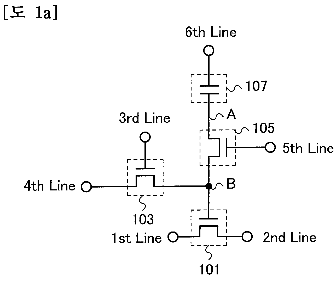
도 1a에 도시된 기억 회로는 제 1 트랜지스터(101), 제 2 트랜지스터(103), 제 3 트랜지스터(105), 및 용량 소자(107)를 구비한다.The memory circuit shown in Fig. 1A includes a
제 1 트랜지스터(101)는 제 1 게이트 전극, 제 1 소스 전극, 및 제 1 드레인 전극을 갖는다.The
제 2 트랜지스터(103)는 제 2 게이트 전극, 제 2 소스 전극, 및 제 2 드레인 전극을 갖는다. 제 2 트랜지스터(103)는 채널 형성 영역에 산화물 반도체를 포함한다.The
제 3 트랜지스터(105)는 제 3 게이트 전극, 제 3 소스 전극, 및 제 3 드레인 전극을 갖는다. 제 3 트랜지스터(105)는 채널 형성 영역에 산화물 반도체를 포함한다.The
제 1 게이트 전극은 제 2 소스 전극 또는 제 2 드레인 전극 중 한쪽 및 제 3 소스 전극 또는 제 3 드레인 전극 중 한쪽과 전기적으로 접속되고, 제 1 소스 전극은 제 1 배선(1st Line)과 전기적으로 접속되고, 제 1 드레인 전극은 제 2 배선(2nd Line)과 전기적으로 접속되고, 제 2 게이트 전극은 제 3 배선(3rd Line)과 전기적으로 접속되고, 제 2 소스 전극 또는 제 2 드레인 전극 중 다른 쪽은 제 4 배선(4th Line)과 전기적으로 접속되고, 제 3 게이트 전극은 제 5 배선(5th Line)과 전기적으로 접속되고, 제 3 소스 전극 또는 제 3 드레인 전극 중 다른 쪽은 용량 소자(107) 중 한쪽 전극과 전기적으로 접속되고, 용량 소자(107) 중 다른 쪽 전극은 제 6 배선(6th Line)과 전기적으로 접속된다.The first gate electrode is electrically connected to one of the second source electrode or the second drain electrode and the third source electrode or the third drain electrode and the first source electrode is electrically connected to the first line And the first drain electrode is electrically connected to the second wiring (2nd Line), the second gate electrode is electrically connected to the third wiring (3rd Line), and the other of the second source electrode and the second drain electrode The third gate electrode is electrically connected to the fifth wiring (5th Line), and the other of the third source electrode and the third drain electrode is electrically connected to the fourth wiring (4th Line) And the other electrode of the
제 1 배선 내지 제 6 배선에 대하여 설명한다. 제 1 배선은 신호가 입력되는 배선이고 예를 들어, 고정 전위가 인가되는 배선을 사용할 수 있다. 제 2 배선은 예를 들어, 판독 회로와 전기적으로 접속된 배선으로 할 수 있다. 제 3 배선은 제 2 트랜지스터(103)의 도통 상태(온 상태 또는 오프 상태)를 선택하는 선택 신호가 입력되는 배선이다. 제 4 배선은 데이터를 포함하는 신호가 주어진 배선이다. 제 5 배선은 제 3 트랜지스터(105)의 도통 상태(온 상태 또는 오프 상태)를 선택하는 선택 신호가 입력되는 배선이다. 제 6 배선은 고정 전위가 인가되는 배선이다. 또한, 제 1 배선 및 제 6 배선은 같은 전위로 할 수 있다.First to sixth wirings will be described. The first wiring is a wiring to which a signal is input, and for example, a wiring to which a fixed potential is applied can be used. The second wiring may be, for example, a wiring electrically connected to the reading circuit. The third wiring is a wiring to which a selection signal for selecting the conduction state (on state or off state) of the
제 1 트랜지스터(101)는 이동도가 높은 것이 바람직하다. 예를 들어, 채널 형성 영역에 다결정 실리콘, 단결정 실리콘 등을 사용함으로써 제 1 트랜지스터(101)의 이동도를 높게 할 수 있다. 제 1 트랜지스터(101)의 이동도가 높으면 높을수록 기억 회로는 데이터의 판독을 짧은 시간에 수행할 수 있다.It is preferable that the
제 1 트랜지스터(101)의 게이트 용량으로서는 제 1 게이트 전극과 채널 형성 영역이 절연막을 개재(介在)하여 적층되는 영역에서 형성되는 용량이나, 제 1 게이트 전극과, 제 1 소스 전극 또는 제 1 드레인 전극이 절연막을 개재하여 적층되는 영역에서 형성되는 용량 등을 들 수 있고, 이들에 의하여 게이트 용량의 크기를 제어할 수 있다.As the gate capacitance of the
제 2 트랜지스터(103) 및 제 3 트랜지스터(105)의 오프 전류는 매우 작은 것이 바람직하다. 제 2 트랜지스터(103) 및 제 3 트랜지스터(105)의 오프 전류가 작으면 작을수록 제 1 트랜지스터(101)의 게이트 용량은 전하를 오랫동안 유지할 수 있다. 또한, 기억 회로에 공급되는 전력이 정지하여도 오랫동안 전하를 유지할 수 있다.The off current of the
제 2 트랜지스터(103) 및 제 3 트랜지스터(105)에는 채널이 형성되는 반도체에 실리콘을 사용한 트랜지스터에 비하여 오프 전류가 저감된 트랜지스터를 사용하는 것이 바람직하다. 구체적으로는 채널이 형성되는 반도체로서 실리콘보다도 밴드 갭이 넓은 반도체를 사용하는 것이 바람직하다. 예를 들어, 밴드 갭이 1.1eV보다 크고, 바람직하게는 2.5eV 이상 4eV 이하, 더 바람직하게는 3eV 이상 3.8eV 이하인 반도체를 사용한다. 실리콘보다도 밴드 갭이 넓은 반도체로서는 예를 들어, 탄소화 실리콘(SiC), 질화 갈륨(GaN) 등의 화합물 반도체, In-Ga-Zn-O계 산화물 반도체 등의 금속 산화물로 이루어진 산화물 반도체 등을 들 수 있다.It is preferable to use a transistor in which a channel is formed in the
또한, 제 2 트랜지스터(103) 및 제 3 트랜지스터(105)의 채널 형성 영역에는 실리콘보다도 진성 캐리어 밀도가 낮은 반도체를 사용하는 것이 바람직하다. 예를 들어, 산화물 반도체의 진성 캐리어 밀도는 10-9/cm3이며, 실리콘의 진성 캐리어 밀도인 1011/cm3에 비하여 매우 작다.It is preferable that a semiconductor having a lower intrinsic carrier density than silicon is used for the channel forming region of the
산화물 반도체를 채널 형성 영역에 사용한 트랜지스터의 다수 캐리어는 트랜지스터의 소스로부터만 흐른다. 또한, 채널 형성 영역을 완전 공핍화하는 것이 가능하므로 트랜지스터의 오프 전류를 매우 작게 할 수 있다. 산화물 반도체가 사용된 트랜지스터의 오프 전류는 실온에서 10yA/μm 이하, 85℃ 내지 95℃에서도 1zA/μm 이하로 매우 작게 하는 것이 가능하다.The majority carriers of the transistors using the oxide semiconductor in the channel forming region flow only from the sources of the transistors. Further, since it is possible to completely deplete the channel forming region, the off current of the transistor can be made very small. The off-state current of the transistor in which the oxide semiconductor is used can be made very small, not more than 10 yA / μm at room temperature and not more than 1 zA / μm even at 85 to 95 ° C.
전자 공여체(도너)가 되는 수분 또는 수소 등의 불순물이 저감되고, 또 산소 결손이 저감됨으로써 고순도화된 산화물 반도체는 i형(진성 반도체) 또는 i형에 한없이 가깝다. 그러므로 상기 산화물 반도체를 사용한 트랜지스터는 오프 전류가 현저히 작다는 특성을 갖는다. 수분 또는 수소 등의 불순물 농도가 충분히 저감되고, 또 산소 결손이 저감됨으로써 고순도화된 산화물 반도체를 사용함으로써 트랜지스터의 오프 전류를 작게 할 수 있다.Impurity such as moisture or hydrogen which becomes an electron donor (donor) is reduced, and the oxygen deficiency is reduced, whereby the highly purified oxide semiconductor is infinitely close to i-type (intrinsic semiconductor) or i-type. Therefore, the transistor using the oxide semiconductor has a characteristic that the off current is remarkably small. The off current of the transistor can be reduced by using an oxide semiconductor which is highly purified by sufficiently reducing impurity concentration such as moisture or hydrogen and reducing oxygen deficiency.
또한, 고순도화된 산화물 반도체의 수소 농도는 2차 이온 질량 분석법(SIMS: Secondary Ion Mass Spectrometry)에 의한 측정값에서 5×10¹⁹atoms/cm3 이하, 바람직하게는 5×10¹⁸atoms/cm3 이하, 더 바람직하게는 5×10¹⁷atoms/cm3 이하인 것이 좋다.In addition, the hydrogen concentration of the oxide semiconductor which has been highly purified is 5 × 10 19 atoms / cm 3 or less, preferably 5 × 10 18 atoms / cm 3 or less, as measured by secondary ion mass spectrometry (SIMS) More preferably 5 x 10 < 17 > atoms / cm < 3 > or less.
또한, 고순도화된 산화물 반도체의 캐리어 밀도는 1×10¹⁴/cm3 미만, 바람직하게는 1×10¹²/cm3 미만, 더 바람직하게는 1×10¹¹/cm3 미만인 것이 좋다.The carrier density of the high purity oxide semiconductor is preferably less than 1 x 10 14 / cm 3 , more preferably less than 1 x 10 12 / cm 3 , and still more preferably less than 1 x 10 11 / cm 3 .
본 발명의 일 형태에 따른 기억 회로는 용량 소자(107) 및 제 1 트랜지스터(101)의 게이트 용량을 사용함으로써 데이터를 오랫동안 유지할 수 있는 제 1 기록 모드와, 제 1 트랜지스터(101)의 게이트 용량을 사용함으로써 데이터를 고속으로 기록할 수 있는 제 2 기록 모드를 구비한다. 본 발명의 일 형태에 따른 기억 회로는 유지하는 용량부를 선택함으로써, 오랫동안 유지할 필요가 있는 데이터는 (양이 많아도) 오랫동안 유지할 수 있고, 짧은 시간에 기록할 필요가 있는 데이터는 고속으로 기록할 수 있다.The memory circuit according to an embodiment of the present invention is configured to have a first recording mode in which data can be held for a long time by using the gate capacitance of the
여기서 용량 소자(107)의 용량은 제 1 트랜지스터(101)의 게이트 용량에 비하여 충분히 큰 것이 바람직하다.It is preferable that the capacitance of the
또한, 도 1b에 도시된 바와 같이, 본 발명의 일 형태에 따른 기억 회로는 용량 소자(109)를 가져도 좋다. 용량 소자(109) 중 한쪽 전극은 제 1 게이트 전극, 제 2 소스 전극 또는 제 2 드레인 전극 중 한쪽, 및 제 3 소스 전극 또는 제 3 드레인 전극 중 한쪽과 전기적으로 접속되고, 다른 쪽 전극은 제 7 배선(7th Line)과 전기적으로 접속되어 있다.1B, the memory circuit according to an aspect of the present invention may have a
다만 용량 소자(109)의 용량은 용량 소자(107)의 용량에 비하여 충분히 작은 것으로 한다.However, it is assumed that the capacitance of the
또한, 제 7 배선은 고정 전위가 인가되는 배선이고, 예를 들어, 제 6 배선과 같은 전위로 할 수 있다.The seventh wiring is a wiring to which a fixed potential is applied. For example, the seventh wiring may have the same potential as the sixth wiring.
<기억 회로의 동작><Operation of Memory Circuit>
도 1a에 도시된 기억 회로의 동작에 대하여 설명한다.The operation of the memory circuit shown in Fig. 1A will be described.
≪제 1 기록 모드≫&Quot; First recording mode "
우선, 용량 소자(107) 및 제 1 트랜지스터(101)의 게이트 용량을 사용한 데이터의 기록, 유지, 및 판독에 대하여 설명한다. 여기서는 용량 소자(107) 중 한쪽 전극 및 제 3 소스 전극 또는 제 3 드레인 전극 중 다른 쪽으로 구성되는 노드를 노드 A라고 기재한다. 또한, 제 1 게이트 전극, 제 2 소스 전극 또는 제 2 드레인 전극 중 한쪽, 및 제 3 소스 전극 또는 제 3 드레인 전극 중 한쪽으로 구성되는 노드를 노드 B라고 기재한다. 또한, 본 실시형태에서 특별히 기재가 없으면 게이트 용량이란 제 1 트랜지스터(101)의 게이트 용량을 가리킨다.First, the recording, holding, and reading of data using the gate capacitance of the
[1-1: 용량 소자(107) 및 게이트 용량을 사용한 데이터의 기록][1-1: Recording of data using the
제 3 배선의 전위를 제 2 트랜지스터(103)가 온 상태가 되는 전위로 하고, 또 제 5 배선의 전위를 제 3 트랜지스터(105)가 온 상태가 되는 전위로 함으로써 제 2 트랜지스터(103) 및 제 3 트랜지스터(105)를 온 상태로 한다. 이어서 제 4 배선과 제 6 배선 사이에 원하는 전압을 인가함으로써 용량 소자(107) 및 게이트 용량에 전하가 축적되어, 노드 A 및 노드 B에 전위가 인가된다(데이터의 기록).The potential of the third wiring is set to the ON state and the potential of the fifth wiring is set to the potential for turning on the
[1-2: 용량 소자(107) 및 게이트 용량을 사용한 데이터의 유지][1-2: Data Retention Using
제 3 배선의 전위를 제 2 트랜지스터(103)가 오프 상태가 되는 전위로 하고, 또 제 5 배선의 전위를 제 3 트랜지스터(105)가 오프 상태가 되는 전위로 함으로써 제 2 트랜지스터(103) 및 제 3 트랜지스터(105)를 오프 상태로 한다. 이로써 노드 A 및 노드 B에 인가된 전위가 유지된다(데이터의 유지). 또한, 여기서는 제 3 트랜지스터(105)를 오프 상태로 함과 동시에, 또는 오프 상태로 한 후에 제 2 트랜지스터(103)를 오프 상태로 한다.By setting the potential of the third wiring to the potential at which the
여기서 제 2 트랜지스터(103) 및 제 3 트랜지스터(105)의 오프 전류는 매우 작기 때문에 용량 소자(107) 및 게이트 용량에 축적된 전하는 오랫동안 유지된다.Here, since the off currents of the
[1-3: 용량 소자(107) 및 게이트 용량을 사용한 데이터의 판독][1-3: Read of data using the
판독을 수행할 때, 제 1 배선에는 소정의 전위(정전위)가 인가된다. 제 5 배선의 전위를 제 3 트랜지스터(105)가 온 상태가 되는 전위로 함으로써 제 3 트랜지스터(105)를 온 상태로 한다. 여기서 노드 A에 제 1 트랜지스터(101)를 온 상태로 하는 전위가 유지되어 있는 경우에는 제 2 배선의 전위가 변화한다. 한편, 노드 A에 제 1 트랜지스터(101)를 오프 상태로 하는 전위가 유지되어 있는 경우에는 제 2 배선의 전위는 변화하지 않는다. 따라서, 제 2 배선의 전위의 변화를 검지함으로써 기억 회로에 기록된 데이터를 판독할 수 있다.When reading is performed, a predetermined potential (positive potential) is applied to the first wiring. The potential of the fifth wiring is set to the potential at which the
[1-4: 용량 소자(107) 및 게이트 용량을 사용한 데이터의 재기록][1-4: Rewriting of data using
데이터의 재기록은 상술한 데이터의 기록 및 유지와 같은 동작으로 수행할 수 있다. 제 2 트랜지스터(103) 및 제 3 트랜지스터(105)를 온 상태로 하고 제 4 배선과 제 6 배선 사이에 새로운 데이터에 따른 전압을 인가함으로써 용량 소자(107) 및 게이트 용량에 전하가 축적되어 노드 A 및 노드 B에 전위가 인가된다(데이터의 기록). 그 후, 제 2 트랜지스터(103) 및 제 3 트랜지스터(105)를 오프 상태로 함으로써 노드 A 및 노드 B에 전위(새로운 데이터에 따른 전위)가 유지된다.Rewriting of data can be performed by operations such as recording and maintaining the above-described data. When the
용량 소자(107) 및 제 1 트랜지스터(101)의 게이트 용량을 사용하여 데이터를 유지함으로써 제 1 트랜지스터(101)의 게이트 용량만을 사용하여 데이터를 유지하는 경우에 비하여 데이터를 오랫동안 유지할 수 있다.The data can be held for a long period of time as compared with a case where data is held using only the gate capacitance of the
≪제 2 기록 모드≫&Quot; Second recording mode "
다음에 제 1 트랜지스터(101)의 게이트 용량만을 사용한 데이터의 기록, 유지, 및 판독에 대하여 설명한다.Next, recording, holding, and reading of data using only the gate capacitance of the
[2-1: 게이트 용량을 사용한 데이터의 기록][2-1: Data recording using gate capacity]
제 5 배선의 전위를 제 3 트랜지스터(105)가 오프 상태가 되는 전위로 함으로써, 제 3 트랜지스터(105)를 오프 상태로 한다. 또한, 제 3 배선의 전위를 제 2 트랜지스터(103)가 온 상태가 되는 전위로 함으로써, 제 2 트랜지스터(103)를 온 상태로 한다. 이어서 제 4 배선에 원하는 전위를 인가함으로써 게이트 용량에 전하가 축적되어 노드 B에 전위가 인가된다(데이터의 기록).The potential of the fifth wiring is set to the potential at which the
[2-2: 게이트 용량을 사용한 데이터의 유지][2-2: Maintaining Data Using Gate Capacity]
제 3 배선의 전위를 제 2 트랜지스터(103)가 오프 상태가 되는 전위로 함으로써 제 2 트랜지스터(103)를 오프 상태로 한다. 이로써 노드 B에 인가된 전위가 유지된다(데이터의 유지).The potential of the third wiring is set to the potential at which the
여기서 제 2 트랜지스터(103) 및 제 3 트랜지스터(105)의 오프 전류는 매우 작기 때문에 게이트 용량에 축적된 전하는 오랫동안 유지된다.Here, since the off currents of the
[2-3: 게이트 용량을 사용한 데이터의 판독][2-3: Reading of data using gate capacitance]
판독을 수행할 때, 제 1 배선에는 원하는 전위(정전위)가 인가된다. 여기서 노드 B에 제 1 트랜지스터(101)를 온 상태로 하는 전위가 유지되어 있는 경우에는 제 2 배선의 전위가 변화한다. 한편, 노드 B에 제 1 트랜지스터(101)를 오프 상태로 하는 전위가 유지되어 있는 경우에는 제 2 배선의 전위는 변화하지 않는다. 따라서, 제 2 배선의 전위의 변화를 검지함으로써 기억 회로에 기록된 데이터를 판독할 수 있다.When reading is performed, a desired potential (positive potential) is applied to the first wiring. Here, when the potential for turning on the
[2-4: 게이트 용량을 사용한 데이터의 재기록][2-4: Rewriting data using gate capacity]
데이터의 재기록은 상술한 데이터의 기록 및 유지와 같은 동작으로 수행할 수 있다. 제 2 트랜지스터(103)를 온 상태로 하고(제 3 트랜지스터(105)는 계속 오프 상태다) 제 4 배선에 새로운 데이터에 따른 전위를 인가함으로써 게이트 용량에 전하가 축적되어 노드 B에 전위가 인가된다(데이터의 기록). 그 후, 제 2 트랜지스터(103)를 오프 상태로 함으로써 노드 B의 전위(새로운 데이터에 따른 전위)가 유지된다.Rewriting of data can be performed by operations such as recording and maintaining the above-described data. The
즉, 본 발명의 일 형태에 따른 기억 회로는 데이터를 다시 기록함으로써 직접 데이터를 재기록할 수 있다. 따라서, 플래시 메모리 등에서 필요하게 되는 소거 동작이 필요 없게 되고, 소거 동작에 기인한 동작 속도의 저하나 소비 전력을 억제할 수 있다.That is, the memory circuit according to an aspect of the present invention can directly rewrite data by rewriting the data. Therefore, the erasing operation required in the flash memory or the like is not required, and the reduction of the operating speed and the power consumption due to the erasing operation can be suppressed.
특히, 게이트 용량만을 사용하여 데이터를 유지함으로써, 용량 소자(107)도 사용하여 데이터를 유지하는 경우에 비하여 기록을 고속으로 수행할 수 있다.Particularly, the data can be held at high speed by using only the gate capacitance, as compared with the case where the data is held using the
<유지 시간과 기록 시간을 계산하는 예><Example of calculating the holding time and recording time>
제 1 트랜지스터(101)의 게이트 용량을 사용한 경우에서의, 데이터를 유지할 수 있는 시간과 데이터를 기록할 때에 걸린 시간에 대하여 계산한 예를 나타낸다. 이하에서는 제 2 트랜지스터(103) 및 제 3 트랜지스터(105)의 채널 형성 영역에 산화물 반도체를 사용하고, 제 1 트랜지스터(101)의 게이트 절연막에 막 두께 x가 10nm의 산화 실리콘막을 사용하고, 제 1 트랜지스터(101)의 채널 길이(L) 및 채널 폭(W)을 1μm로 한 경우에 대하여 나타낸다.There is shown an example in which the time for holding the data and the time for recording the data in the case where the gate capacitance of the
제 1 게이트 전극 및 반도체층 사이의 게이트 절연막의 용량(C)은 수학식 (1)에 나타낸 바와 같이, 3.45×10⁻¹⁵F(즉 3.45fF)로 계산될 수 있다. 또한, 수학식 (1)에서 ε은 게이트 절연막의 비유전율을 가리키고, ε0은 진공의 유전율을 가리킨다.The capacitance C of the gate insulating film between the first gate electrode and the semiconductor layer can be calculated to be 3.45 x 10 -15 F (i.e., 3.45 fF), as shown in equation (1). In Equation (1),? Denotes the relative dielectric constant of the gate insulating film, and? 0 denotes the dielectric constant of the vacuum.
![]()
![]()
제 2 트랜지스터(103) 및 제 3 트랜지스터(105)의 오프 전류(Ioff)를 10yA, 제 1 트랜지스터(101)의 게이트 용량을 사용하여 데이터를 유지할 때의 게이트 전압(유지 전압)(V)을 3V로 하면, 유지 전하가 10% 감소할 때까지의 시간(t1)은 수학식 (2)에 나타낸 바와 같이, 5.175×10⁷s로 계산될 수 있고, 즉 1년 반 이상인 것을 알 수 있다. 또한, 용량 소자(107)를 사용하여, 데이터를 유지하는 경우에는 제 1 트랜지스터(101)의 게이트 용량만을 사용하여 데이터를 유지할 경우보다도 용량이 크게 되기 때문에 유지 전하가 10% 감소할 때까지의 시간이 t1보다 길다.The off current (I off ) of the
![]()
![]()
또한, 제 2 트랜지스터(103)의 온 전류(Ion)를 5μA로 하면, 제 1 트랜지스터(101)의 게이트 용량에 데이터에 의거한 전하를 기록하는 시간(t2)은 2.07×10⁻⁹s(즉, 2.07ns)로 계산될 수 있다.In addition, the
![]()
![]()
이상에 의하여, 채널 형성 영역에 산화물 반도체를 사용한 제 2 트랜지스터(103) 및 제 3 트랜지스터(105)를 적용한 본 발명의 일 형태에 따른 기억 회로에서는 게이트 용량을 사용하여 데이터를 오랫동안 유지할 수 있고, 또 고속으로 데이터를 기록할 수 있는 것을 알 수 있었다.Thus, in the storage circuit according to an embodiment of the present invention in which the
<산화물 반도체><Oxide Semiconductor>
또한, 본 발명의 일 형태에 따른 기억 회로는 채널 형성 영역에 산화물 반도체를 사용한 트랜지스터를 구비한다. 이하에 산화물 반도체에 대하여 설명한다.Further, a memory circuit according to an aspect of the present invention includes a transistor using an oxide semiconductor in a channel forming region. The oxide semiconductor will be described below.
산화물 반도체는, 단결정, 다결정(폴리크리스탈), 또는 비정질(어모퍼스) 등의 상태를 갖는다.The oxide semiconductor has a state such as a single crystal, a polycrystalline (polycrystal), or an amorphous (amorphous) state.
어모퍼스 상태의 산화물 반도체는 비교적 쉽게 평탄한 표면을 얻을 수 있기 때문에, 상기 어모퍼스 상태의 산화물 반도체를 사용한 트랜지스터는 동작시켰을 때의 캐리어 (전자의) 계면 산란을 저감할 수 있고, 비교적 쉽게 높은 전계 효과 이동도를 얻을 수 있다.Since the amorphous oxide semiconductor can obtain a relatively easily flat surface, the transistor using the amorphous oxide semiconductor can reduce the interfacial scattering of the carrier (electrons) when the transistor is operated, and the relatively high field effect mobility Can be obtained.
또한, 결정성을 갖는 산화물 반도체에서는, 벌크 내 결함을 더 저감시킬 수 있고, 표면의 평탄성을 높이면 상기 결정성을 갖는 산화물 반도체는 어모퍼스 상태의 산화물 반도체를 사용한 트랜지스터에 비하여 높은 전계 효과 이동도를 얻을 수 있다. 표면의 평탄성을 높이기 위해서는 평탄한 표면 위에 산화물 반도체를 형성하는 것이 바람직하다.Further, in the oxide semiconductor having crystallinity, it is possible to further reduce the defects in the bulk, and if the surface flatness is increased, the oxide semiconductor having the above crystallinity can attain a higher field effect mobility than the transistor using the amorphous oxide semiconductor . In order to increase the flatness of the surface, it is preferable to form an oxide semiconductor on a flat surface.
산화물 반도체는 예를 들어, 비단결정을 가져도 좋다. 비단결정은 예를 들어, CAAC(C Axis Aligned Crystal), 다결정, 미결정, 비정질부를 갖는다. 비정질부는, 미결정, CAAC보다 결함 준위 밀도가 높다. 또한, 미결정은 CAAC보다 결함 준위 밀도가 높다. 또한, CAAC를 갖는 산화물 반도체를 CAAC-OS(C Axis Aligned Crystalline Oxide Semiconductor)라고 부른다.The oxide semiconductor may have, for example, a non-crystal shape. The non-single crystal has, for example, a C-Axis Aligned Crystal (CAAC), a polycrystalline, a microcrystalline, and an amorphous portion. The amorphous portion is undecrystallized and has a higher defect level density than CAAC. In addition, microcrystalline has a higher defect level density than CAAC. Further, an oxide semiconductor having CAAC is called CAAC-OS (C Axis Aligned Crystalline Oxide Semiconductor).
산화물 반도체막은 예를 들어, CAAC-OS를 가져도 좋다. CAAC-OS는 예를 들어, c축 배향하고, a축 또는/및 b축은 거시적으로 보면 정렬되어 있지 않다.The oxide semiconductor film may have, for example, CAAC-OS. CAAC-OS, for example, is c-axis oriented and the a-axis or / and b-axis are not aligned macroscopically.
산화물 반도체막은 예를 들어, 미결정을 가져도 좋다. 미결정을 갖는 산화물 반도체(미결정 산화물 반도체라고도 함)막은 예를 들어, 막 중에 1nm 이상 10nm 미만의 사이즈의 미결정(나노 결정이라고도 함)을 포함한다.The oxide semiconductor film may have a microcrystalline structure, for example. An oxide semiconductor (also referred to as a microcrystalline oxide semiconductor) having microcrystallization includes, for example, microcrystalline (also referred to as nanocrystal) having a size of 1 nm or more and less than 10 nm in the film.
산화물 반도체막은 예를 들어, 비정질부를 가져도 좋다. 비정질부를 갖는 산화물 반도체(비정질 산화물 반도체라고도 함)막은 예를 들어, 원자 배열이 무질서한 막이고, 결정 성분이 없다. 또는 비정질 산화물 반도체막은 예를 들어, 완전한 비정질이고, 결정부를 갖지 않는다.The oxide semiconductor film may have, for example, an amorphous portion. An oxide semiconductor (also referred to as an amorphous oxide semiconductor) film having an amorphous portion is, for example, a disordered film of atoms and has no crystal component. Or the amorphous oxide semiconductor film is, for example, completely amorphous and has no crystal part.
또한, 산화물 반도체막이 CAAC-OS, 미결정 산화물 반도체, 비정질 산화물 반도체의 혼합막이어도 좋다. 혼합막은 예를 들어, 비정질 산화물 반도체의 영역과, 미결정 산화물 반도체의 영역과, CAAC-OS의 영역을 갖는다. 또한, 혼합막은 예를 들어, 비정질 산화물 반도체의 영역과, 미결정 산화물 반도체의 영역과, CAAC-OS의 영역의 적층 구조를 가져도 좋다.Further, the oxide semiconductor film may be a mixed film of CAAC-OS, a microcrystalline oxide semiconductor, and an amorphous oxide semiconductor. The mixed film has, for example, a region of an amorphous oxide semiconductor, a region of a microcrystalline oxide semiconductor, and a region of a CAAC-OS. Further, the mixed film may have, for example, a laminated structure of a region of an amorphous oxide semiconductor, a region of a microcrystalline oxide semiconductor, and a region of a CAAC-OS.
또한, 산화물 반도체막은 예를 들어, 단결정을 가져도 좋다.Further, the oxide semiconductor film may have, for example, a single crystal.
산화물 반도체막은 결정부를 복수로 갖고, 상기 결정부의 c축이 피형성면의 법선 벡터 또는 표면의 법선 벡터에 평행한 방향으로 정렬되어 있는 것이 바람직하다. 또한, 상이한 결정부들 사이에서 a축 및 b축의 방향이 각각 상이하여도 좋다. 이와 같은 산화물 반도체막의 일례로서는, CAAC-OS막이 있다.It is preferable that the oxide semiconductor film has a plurality of crystal portions and the c axis of the crystal portion is aligned in a direction parallel to the normal vector of the surface to be formed or the normal vector of the surface. Further, the directions of the a-axis and the b-axis may be different from each other between the different crystal portions. An example of such an oxide semiconductor film is a CAAC-OS film.
본 발명의 일 형태에서 산화물 반도체를 사용한 반도체층으로서는 CAAC-OS막이 바람직하다.In one embodiment of the present invention, the semiconductor layer using an oxide semiconductor is preferably a CAAC-OS film.
CAAC-OS막에 포함되는 결정부는 하나의 변이 100nm 미만의 입방체 내에 들어가는 크기인 경우가 많다. 또한, 투과형 전자 현미경(TEM: Transmission Electron Microscope)에 의한 관찰상에서는 CAAC-OS막에 포함되는 결정부와 결정부의 경계는 명확하지 않다. 또한, TEM에 의하여 CAAC-OS막에 명확한 입계(그레인 바운더리라고도 함)는 확인되지 않는다. 그래서, CAAC-OS막은 입계에 기인하는 전자 이동도의 저하가 억제된다.The crystal part included in the CAAC-OS film often has a size such that one side falls within a cube of less than 100 nm. In addition, the boundary between the crystal part and the crystal part included in the CAAC-OS film is not clear on the observation by a transmission electron microscope (TEM). Also, no clear grain boundaries (also called grain boundaries) are identified in the CAAC-OS film by TEM. Thus, the CAAC-OS film is suppressed from lowering the electron mobility due to the grain boundary.
CAAC-OS막에 포함되는 결정부는 예를 들어, c축이 CAAC-OS막의 피형성면의 법선 벡터 또는 표면의 법선 벡터에 평행한 방향이 되도록 정렬되고, 또 ab면에 수직인 방향에서 볼 때 금속 원자가 삼각형 또는 육각형으로 배열되며, c축에 수직인 방향에서 볼 때 금속 원자가 층상 또는 금속 원자와 산소 원자가 층상으로 배열되어 있다. 또한, 상이한 결정부들 사이에서 a축 및 b축의 방향이 각각 상이하여도 좋다. 본 명세서에서, 단순히 “수직”이라고 기재한 경우, 80° 이상 100° 이하의 범위, 바람직하게는 85° 이상 95° 이하의 범위도 포함되는 것으로 한다. 또한, 단순히 “평행”이라고 기재한 경우에는 -10° 이상 10° 이하의 범위, 바람직하게는 -5° 이상 5° 이하의 범위도 포함되는 것으로 한다.The crystal part included in the CAAC-OS film is, for example, aligned such that the c-axis is parallel to the normal vector of the surface to be formed or the normal vector of the surface of the CAAC-OS film, and when viewed in a direction perpendicular to the ab- The metal atoms are arranged in a triangle or a hexagon, and when seen in a direction perpendicular to the c axis, the metal atoms are arranged in layers or in the form of layers of metal atoms and oxygen atoms. Further, the directions of the a-axis and the b-axis may be different from each other between the different crystal portions. In the present specification, when simply referred to as " vertical ", it is assumed that the range of 80 DEG to 100 DEG, preferably 85 DEG to 95 DEG is also included. In the case of simply describing "parallel", it is assumed that the range of -10 ° to 10 °, preferably -5 ° to 5 °, is also included.
또한, CAAC-OS막에서 결정부의 분포가 균일하지 않아도 좋다. 예를 들어, CAAC-OS막의 형성 과정에서 산화물 반도체막의 표면 측으로부터 결정 성장시키는 경우에는, 피형성면 근방보다 표면 근방에서 결정부가 차지하는 비율이 높은 경우가 있다. 또한, CAAC-OS막에 불순물을 첨가함으로써 상기 불순물 첨가 영역에서 결정부의 결정성이 저하하는 경우도 있다.Also, the distribution of the crystal portions in the CAAC-OS film need not be uniform. For example, when the crystal is grown from the surface side of the oxide semiconductor film in the process of forming the CAAC-OS film, the proportion of the crystal portion in the vicinity of the surface may be higher than in the vicinity of the surface to be formed. In addition, by adding an impurity to the CAAC-OS film, the crystallinity of the crystalline portion in the impurity added region may be lowered.
CAAC-OS막에 포함되는 결정부의 c축은, CAAC-OS막의 피형성면의 법선 벡터 또는 표면의 법선 벡터에 평행한 방향이 되도록 정렬되기 때문에, CAAC-OS막의 형상(피형성면의 단면 형상 또는 표면의 단면 형상)에 따라서는 서로 상이한 방향을 향하는 경우가 있다. 또한, 성막하였을 때 또는 성막한 후에 가열 처리 등의 결정화 처리를 수행하였을 때, 결정부는 형성된다. 따라서, 결정부의 c축은, CAAC-OS막이 형성되었을 때의 피형성면의 법선 벡터 또는 표면의 법선 벡터에 평행한 방향이 되도록 정렬된다.Since the c-axis of the crystal part included in the CAAC-OS film is aligned so as to be parallel to the normal vector of the surface to be formed or the normal vector of the surface of the CAAC-OS film, the shape of the CAAC- The cross-sectional shape of the surface) may be different from each other. Further, when a crystallization process such as a heat treatment is performed when the film is formed or after the film is formed, a crystal portion is formed. Therefore, the c-axis of the crystal part is aligned so as to be parallel to the normal vector of the surface to be formed or the normal vector of the surface when the CAAC-OS film is formed.
CAAC-OS막을 사용함으로써 가시광이나 자외광의 조사에 기인한 트랜지스터의 전기 특성의 변동이 저감되기 때문에 신뢰성이 높은 트랜지스터를 얻을 수 있다.By using the CAAC-OS film, fluctuations in the electrical characteristics of the transistor due to irradiation of visible light and ultraviolet light are reduced, so that a highly reliable transistor can be obtained.
산화물 반도체로서는 적어도 인듐(In) 또는 아연(Zn)을 포함하는 것이 바람직하다. 특히 In과 Zn 양쪽 모두를 포함하는 것이 바람직하다. 또한, 상기 산화물 반도체가 사용되는 트랜지스터의 전기 특성의 편차를 저감시키기 위한 스테빌라이저로서 이들에 더하여 갈륨(Ga)을 갖는 것이 바람직하다. 또한, 스테빌라이저로서 주석(Sn)을 갖는 것이 바람직하다. 또한, 스테빌라이저로서 하프늄(Hf)을 갖는 것이 바람직하다. 또한, 스테빌라이저로서 알루미늄(Al)을 갖는 것이 바람직하다. 또한, 스테빌라이저로서 지르코늄(Zr)을 갖는 것이 바람직하다.The oxide semiconductor preferably includes at least indium (In) or zinc (Zn). It is particularly preferable to include both In and Zn. Further, it is preferable to use gallium (Ga) as a stabilizer for reducing the variation in electric characteristics of the transistor in which the oxide semiconductor is used. Further, it is preferable to have tin (Sn) as a stabilizer. Further, it is preferable to have hafnium (Hf) as a stabilizer. Further, it is preferable to have aluminum (Al) as a stabilizer. Further, it is preferable to have zirconium (Zr) as a stabilizer.
또한, 다른 스테빌라이저로서, 란타노이드인 란타넘(La), 세륨(Ce), 프라세오디뮴(Pr), 네오디뮴(Nd), 사마륨(Sm), 유로퓸(Eu), 가돌리늄(Gd), 테르븀(Tb), 디스프로슘(Dy), 홀뮴(Ho), 에르븀(Er), 툴륨(Tm), 이테르븀(Yb), 루테튬(Lu) 중에서 선택된 어느 1종류 또는 복수 종류를 가져도 좋다.As another stabilizer, lanthanoids such as lanthanum La, cerium, praseodymium Pr, neodymium, samarium, europium Eu, gadolinium Gd, terbium Tb, , Dysprosium (Dy), holmium (Ho), erbium (Er), thulium (Tm), ytterbium (Yb), and lutetium (Lu).
예를 들어, 산화물 반도체로서 산화 인듐, 산화 주석, 산화 아연, 2원계 금속 산화물인, In-Zn계 산화물, Sn-Zn계 산화물, Al-Zn계 산화물, Zn-Mg계 산화물, Sn-Mg계 산화물, In-Mg계 산화물, In-Ga계 산화물, 3원계 금속 산화물인, In-Ga-Zn계 산화물, In-Al-Zn계 산화물, In-Sn-Zn계 산화물, Sn-Ga-Zn계 산화물, Al-Ga-Zn계 산화물, Sn-Al-Zn계 산화물, In-Hf-Zn계 산화물, In-La-Zn계 산화물, In-Ce-Zn계 산화물, In-Pr-Zn계 산화물, In-Nd-Zn계 산화물, In-Sm-Zn계 산화물, In-Eu-Zn계 산화물, In-Gd-Zn계 산화물, In-Tb-Zn계 산화물, In-Dy-Zn계 산화물, In-Ho-Zn계 산화물, In-Er-Zn계 산화물, In-Tm-Zn계 산화물, In-Yb-Zn계 산화물, In-Lu-Zn계 산화물, 4원계 금속 산화물인, In-Sn-Ga-Zn계 산화물, In-Hf-Ga-Zn계 산화물, In-Al-Ga-Zn계 산화물, In-Sn-Al-Zn계 산화물, In-Sn-Hf-Zn계 산화물, In-Hf-Al-Zn계 산화물을 사용할 수 있다.Examples of the oxide semiconductor include indium oxide, tin oxide, zinc oxide, binary oxide, In-Zn oxide, Sn-Zn oxide, Al-Zn oxide, Zn-Mg oxide, Sn-Mg oxide In-Zn-based oxide, In-Sn-Zn-based oxide, Sn-Ga-Zn-based oxide, In-Mg-based oxide, In-Ga-based oxide, ternary metal oxide, Zn-based oxide, In-Ce-Zn-based oxide, In-Pr-Zn-based oxide, In-La-Zn-based oxide, In-Zn-based oxide, In-Sm-Zn-based oxide, In-Eu-Zn-based oxide, In-Gd-Zn-based oxide, In-Tb- In-Sn-Ga-Zn-Zn-based oxide, which is a quaternary metal oxide, such as an In-Sn-Zn-based oxide, an In-Er-Zn-based oxide, an In- Zn-based oxide, In-Hf-Ga-Zn-based oxide, In-Al-Ga-Zn-based oxide, In-Sn- Zn-based oxide can be used.
이상에 기재된 바와 같이, 본 발명의 일 형태에 따른 기억 회로는 오랫동안 유지할 필요가 있는 데이터는 오랫동안 유지할 수 있고, 짧은 시간에 기록할 필요가 있는 데이터는 고속으로 기록할 수 있다. 본 발명의 일 형태에 따른 기억 회로는 고속으로 동작을 수행하는 모드와, 데이터를 오랫동안 유지하는 모드로 적절히 전환시켜 사용할 수 있다.As described above, the memory circuit according to an aspect of the present invention can keep data that needs to be held for a long time for a long time, and can record data that needs to be written in a short time at a high speed. The memory circuit according to an embodiment of the present invention can be used by appropriately switching to a mode for performing an operation at a high speed and a mode for retaining data for a long time.
본 실시형태는 다른 실시형태와 적절히 조합하여 실시할 수 있다.The present embodiment can be implemented in appropriate combination with other embodiments.
(실시형태 2)(Embodiment 2)
본 실시형태에서는 본 발명의 일 형태에 따른 기억 회로의 제작 방법에 대하여 도 2 내지 도 4e를 사용하여 설명한다. 도 2에 본 발명의 일 형태에 따른 기억 회로의 평면도의 일례를 도시하였다. 도 2를 A-B로 자른 단면도를 도 3a에 도시하였고, 도 2를 C-D로 자른 단면도를 도 3b에 도시하였고, 도 2를 E-F로 자른 단면도를 도 3c에 도시하였다. 또한, 본 실시형태에 기재된 기억 회로의 회로도는 도 1a에 상당한다.In this embodiment, a method of manufacturing a memory circuit according to an embodiment of the present invention will be described with reference to Figs. 2 to 4E. 2 shows an example of a top view of a memory circuit according to an embodiment of the present invention. FIG. 3 is a cross-sectional view taken along line A-B of FIG. 2, FIG. 3 is a cross-sectional view taken along line C-D of FIG. 2, and FIG. 3 is a cross-sectional view taken along line E-F of FIG. The circuit diagram of the memory circuit described in this embodiment corresponds to Fig. 1A.
우선, 기판(221) 위에 n채널형의 제 1 트랜지스터(101)를 제작한다. 여기서는 일례로서 단결정의 반도체 기판으로부터 분리된 단결정 반도체막을 사용하여 n채널형의 제 1 트랜지스터(101)를 제작한다.First, an n-channel type
도 3b에 도시된 제 1 트랜지스터(101)는 게이트 전극(203)을 갖는다. 제 1 트랜지스터(101)는 반도체층(201) 내에 게이트 전극(203)과 중첩된 영역을 끼우도록 형성된 한 쌍의 n형 도전성을 갖는 영역을 포함한다. 그리고 제 1 트랜지스터(101)는 반도체층(201)과 게이트 전극(203) 사이에 게이트 절연막(225)을 갖는다.The
구체적인 단결정 반도체막의 제작 방법의 일례에 대하여 간단하게 설명한다. 우선 단결정의 반도체 기판에 전계에 의하여 가속된 이온으로 이루어진 이온 빔을 주입하여, 반도체 기판 표면으로부터 일정한 깊이의 영역에 결정 구조가 흩뜨려짐으로써 부분적으로 취약화된 취화(脆化)층을 형성한다. 취화층이 형성되는 영역의 깊이는 이온 빔의 가속 에너지와 이온 빔의 입사각에 의하여 조절할 수 있다. 그리고, 반도체 기판과 절연막(223)이 형성된 기판(221)을, 상기 절연막(223)을 사이에 끼우도록 접합한다. 접합함에서는, 반도체 기판과 기판(221)을 중첩시킨 후, 반도체 기판과 기판(221)의 일부에 1N/cm2 이상 500N/cm2 이하, 바람직하게는 11N/cm2 이상 20N/cm2 이하 정도의 압력을 가한다. 압력을 가하면, 그 부분으로부터 반도체 기판과 절연막(223)이 접합되기 시작하고, 최종적으로는 밀착된 면 전체가 접합된다. 다음에, 가열 처리를 수행함으로써, 취화층에 존재하는 미소 보이드들끼리 결합하여, 미소 보이드의 체적이 증대된다. 결과적으로, 취화층에서 반도체 기판의 일부인 단결정 반도체막이 반도체 기판으로부터 분리된다. 상기 가열 처리의 온도는, 기판(221)의 변형점을 넘지 않는 온도로 한다. 그리고, 상기 단결정 반도체막을 에칭 등에 의하여 원하는 형상으로 가공함으로써 섬 형상의 반도체층(201)을 형성할 수 있다.An example of a method for manufacturing a specific single crystal semiconductor film will be briefly described. An ion beam composed of ions accelerated by an electric field is injected into a single crystal semiconductor substrate to form a partially weakened embrittlement layer by scattering a crystal structure in a region having a predetermined depth from the surface of the semiconductor substrate . The depth of the region where the brittle layer is formed can be controlled by the acceleration energy of the ion beam and the incident angle of the ion beam. Then, the
또한, 본 실시형태에서는 단결정의 반도체막을 사용하여 제 1 트랜지스터(101)를 제작하는 예에 대하여 설명하지만, 본 발명은 이 구성에 한정되지 않는다. 예를 들어, 절연막(223) 위에 기상 성장법을 사용하여 형성된 다결정, 미결정의 반도체막을 사용하여도 좋고, 상기 반도체막을 공지의 기술에 의하여 결정화시켜도 좋다. 공지의 결정화 방법으로서는, 레이저 광을 사용한 레이저 결정화법, 촉매 원소를 사용하는 결정화법이 있다. 또는, 촉매 원소를 사용하는 결정화법과 레이저 결정화법을 조합하여 사용할 수도 있다. 또한, 석영과 같은 내열성이 우수한 기판을 사용하는 경우, 전열로를 사용한 열결정화법, 적외광을 사용한 램프 어닐링 결정화법, 촉매 원소를 사용하는 결정화법, 950℃ 정도의 고온 어닐링법을 조합한 결정화법을 사용하여도 좋다.In the present embodiment, an example in which the
또한, 제 1 트랜지스터(101)는 실리콘, 게르마늄, 실리콘 게르마늄, 단결정 탄소화 실리콘 등의 반도체 재료를 사용하여 제작할 수 있다. 예를 들어, 실리콘을 사용한 제 1 트랜지스터(101)는 실리콘 웨이퍼 등의 단결정 반도체 기판, SOI법에 의하여 제작된 실리콘 박막, 기상 성장법에 의하여 제작된 실리콘 박막 등을 사용하여 형성할 수 있다.Also, the
기판(221)으로서 사용할 수 있는 소재에 큰 제한은 없지만, 적어도, 나중의 가열 처리에 견딜 수 있을 정도의 내열성을 가지고 있는 것이 필요하다. 예를 들어, 기판(221)에는 퓨전법이나 플로트법으로 제작되는 유리 기판이나, 석영 기판, 세라믹 기판 등을 사용할 수 있다. 유리 기판으로서는, 나중의 가열 처리의 온도가 높은 경우에는, 변형점이 730℃ 이상의 것을 사용하면 좋다. 플라스틱 등의 가요성을 갖는 합성 수지로 이루어지는 기판은, 일반적으로 상기 기판과 비교하여 내열 온도가 낮은 경향이 있지만, 제작 공정에서의 처리 온도에 견딜 수 있는 것이라면 사용하는 것이 가능하다.There is no particular limitation on the material that can be used as the
다음에 제 1 트랜지스터(101)를 덮도록 절연막(227)을 형성한다. 그 후, 게이트 절연막(225) 및 절연막(227)을 부분적으로 에칭함으로써 반도체층(201) 내의 한 쌍의 n형 도전성을 갖는 영역 및 게이트 전극(203)에 도달하는 콘택트 홀을 형성한다. 그리고 절연막(227) 위에 스퍼터링법이나 진공 증착법으로 도전막을 형성하고, 에칭 등에 의하여 상기 도전막을 패터닝함으로써 상기 한 쌍의 n형 도전성을 갖는 영역과 전기적으로 접속되는 도전층(205a) 및 도전층(205b), 및 게이트 전극(203)과 전기적으로 접속되는 도전층(205c)을 형성한다. 더구나, 도전층(205a) 내지 도전층(205c)을 덮도록 절연막(229)을 형성한다.Next, an insulating
절연막(227) 및 절연막(229)은 각각 단층 구조라도 좋고, 적층 구조라도 좋다. 절연막(227) 및 절연막(229)은 그 표면을 CMP법 등에 의하여 평탄화시켜도 좋다. 평탄화된 절연막을 사용함으로써 나중에 형성하는 산화물 반도체층을 갖는 트랜지스터에서의 전기 특성의 편차를 저감할 수 있다. 또한, 산화물 반도체층을 갖는 트랜지스터를 수율 좋게 형성할 수 있다.The insulating
절연막(227) 및 절연막(229)은 나중의 제작 공정에서의 가열 처리의 온도에 견딜 수 있는 재료를 사용한다. 절연막(227)이나 절연막(229)의 재료로서는 예를 들어, 산화 실리콘, 질화 실리콘, 질화 산화 실리콘, 산화 질화 실리콘, 질화 알루미늄, 산화 알루미늄, 산화 갈륨, 산화 질화 알루미늄, 산화 하프늄, 산화 마그네슘, 산화 지르코늄, 산화 란타넘, 산화 바륨 등을 사용할 수 있다.The insulating
또한, 본 명세서에서 산화 질화물이란 그 조성으로서 질소보다도 산소의 함유량이 많은 물질을 가리키고, 또한, 질화 산화물이란 그 조성으로서 산소보다도 질소의 함유량이 많은 물질을 가리킨다.In this specification, the term " oxynitride " refers to a substance having a higher oxygen content than nitrogen as its composition, and a nitride oxide refers to a substance having a nitrogen content higher than that of oxygen as its composition.
나중에 형성되는 산화물 반도체층(207)과 접하는 층인 절연막(229)은 수분이나, 수소 등의 불순물을 가능한 한 포함하지 않는 것이 바람직하다. 절연막(229)에 수소가 포함되면, 그 수소가 산화물 반도체층으로 침입하고, 또는 수소가 산화물 반도체층 중의 산소를 뽑아 산화물 반도체층의 백 채널부가 저저항화(n형화)되어 기생 채널이 형성될 우려가 있다. 따라서, 절연막(229)은 가능한 한 수소를 포함하지 않는 막이 되도록, 성막 방법에 수소를 사용하지 않는 것이 중요하다.It is preferable that the insulating
산화 알루미늄막은 수소, 수분 등의 불순물, 및 산소의 양쪽에 대하여 막을 통과시키지 않는 차단 효과(블로킹 효과)가 높고 제작 공정 중 및 제작한 후에서 변동 요인이 되는 수소, 수분 등의 불순물의 산화물 반도체층(207)으로의 혼입, 및 산화물 반도체를 구성하는 주성분 재료인 산소의 산화물 반도체층(207)으로부터의 방출을 방지하는 보호막으로서 기능하기 때문에 바람직하게 사용할 수 있다.The aluminum oxide film has a high blocking effect (blocking effect) that does not allow the film to pass through both the impurities such as hydrogen, moisture, and oxygen, and the impurity such as hydrogen and moisture, which is a fluctuation factor in the fabrication process, It functions as a protective film for preventing the introduction of oxygen into the
절연막(229)은 산화물 반도체층(207)과 접하는 부분에 산소를 포함하는 것이 바람직하다. 특히, 절연막(229)은 막 내(벌크 내)에 적어도 화학량론적 조성을 초과하는 양의 산소가 존재하는 것이 바람직하고, 예를 들어, 절연막(229)으로서 산화 실리콘막을 사용하는 경우에는, SiO2 +α(다만, α>0)로 하는 것이 바람직하다. 이 산화 실리콘막을 절연막(229)으로서 사용함으로써, 산화물 반도체층(207)으로 산소를 공급할 수 있고 특성을 양호하게 할 수 있다.It is preferable that the insulating
또한, 절연막(229)을 적층 구조로 하는 경우, 산화물 반도체층(207)과 접하는 산화물 절연막과, 산화물 절연막과 접하는 배리어성이 높은 절연막의 적층 구조가 바람직하다. 예를 들어, 배리어성이 높은 절연막으로서, 질화 실리콘막, 질화 산화 실리콘막, 질화 알루미늄막, 또는 질화 산화 알루미늄막 등을 사용할 수 있다. 배리어성이 높은 절연막을 사용함으로써 산화물 반도체층(207) 내 등에 수분 또는 수소 등의 불순물이 들어가는 것을 방지할 수 있다.When the insulating
도전층(205a) 내지 도전층(205c)의 재료로서는 예를 들어, 알루미늄, 크로뮴, 구리, 탄탈럼, 티타늄, 몰리브데넘, 텅스텐으로부터 선택된 원소, 상술한 원소를 성분으로 하는 합금이나, 또는 상술한 원소를 조합시킨 합금 등을 들 수 있다. 또한 알루미늄, 구리 등의 금속막의 아래측 또는 위측에 크로뮴, 탄탈럼, 티타늄, 몰리브데넘, 텅스텐 등의 고융점 금속막을 적층시킨 구성으로 하여도 좋다. 또한 알루미늄 또는 구리는 내열성이나 부식성의 문제를 회피하기 위하여 고융점 금속 재료와 조합시켜서 이용하면 좋다. 고융점 금속 재료로서는 몰리브데넘, 티타늄, 크로뮴, 탄탈럼, 텅스텐, 네오디뮴, 스칸듐, 이트륨 등을 사용할 수 있다.As the material of the
또한, 도전층(205a) 내지 도전층(205c)은 단층 구조이어도 좋고 2층 이상의 적층 구조이어도 좋다. 예를 들어, 실리콘을 포함하는 알루미늄막의 단층 구조, 알루미늄막 위에 티타늄막을 적층하는 2층 구조, 티타늄막과 그 티타늄막 위에 중첩시켜 알루미늄막을 적층하고, 더구나 그 위에 티타늄막을 형성하는 3층 구조 등을 들 수 있다.The
또한, 도전층(205a) 내지 도전층(205c)은 도전성 금속 산화물로 형성하여도 좋다. 도전성 금속 산화물로서는 산화 인듐, 산화 주석, 산화 아연, 인듐 주석 산화물, 인듐 아연 산화물 또는 상기 금속 산화물 재료에 실리콘 또는 산화 실리콘을 포함시킨 것을 사용할 수 있다.The
도전막을 형성한 후에 가열 처리를 수행하는 경우에는, 상기 가열 처리에 견딜 수 있는 내열성을 도전막에 부여하는 것이 바람직하다.In the case where the heat treatment is performed after the formation of the conductive film, it is preferable to impart heat resistance to the conductive film to the heat treatment.
다음에 절연막(229) 위에 산화물 반도체층(207)을 형성한다. 산화물 반도체에 대해서는 상술한 실시형태에서의 설명도 함께 참작할 수 있다.Next, an
산화물 반도체층(207)은 단층 구조이어도 좋고, 적층 구조이어도 좋다. 또한, 비정질 구조로 하여도 좋고, 결정성 산화물 반도체로 하여도 좋다. 산화물 반도체층(207)을 비정질 구조로 하는 경우에는, 나중의 제작 공정에서 산화물 반도체층에 가열 처리를 수행함으로써, 결정성 산화물 반도체층으로 하여도 좋다. 비정질 산화물 반도체층을 결정화시키는 가열 처리의 온도는, 250℃ 이상 700℃ 이하, 바람직하게는 400℃ 이상, 더 바람직하게는 500℃ 이상, 더욱 바람직하게는 550℃ 이상으로 한다. 또한, 상기 가열 처리는, 제작 공정에서의 다른 가열 처리를 겸할 수도 있다.The
산화물 반도체층(207)의 형성 방법은, 스퍼터링법, MBE(Molecular Beam Epitaxy)법, CVD법, 펄스레이저 퇴적법, ALD(Atomic Layer Deposition)법 등을 적절히 사용할 수 있다. 또한, 산화물 반도체층(207)은 스퍼터링 타깃 표면에 대하여 대략 수직으로 복수의 기판 표면이 고정된 상태로 막을 형성하는 스퍼터링 장치를 사용하여 형성하여도 좋다.The
산화물 반도체층(207)을 형성할 때, 산화물 반도체층(207)에 포함되는 수소 농도를 가능한 한 저감시키는 것이 바람직하다. 수소 농도를 저감시키기 위해서는, 예를 들어, 스퍼터링법을 사용하여 막을 형성하는 경우에는 스퍼터링 장치의 성막실 내에 공급하는 분위기 가스로서, 수소, 물, 수산기 또는 수소화물 등의 불순물이 제거된 고순도의 희가스(대표적으로는 아르곤), 산소, 및 희가스와 산소의 혼합 가스를 적절히 사용한다.When the
또한, 성막실 내의 잔류 수분을 제거하면서, 수소 및 수분이 제거된 스퍼터링 가스를 도입하여 막을 형성함으로써, 형성된 산화물 반도체층의 수소 농도를 저감시킬 수 있다. 성막실 내의 잔류 수분을 제거하기 위해서는, 흡착형 진공 펌프, 예를 들어, 크라이오 펌프, 이온 펌프, 티타늄 서블리메이션 펌프를 사용하는 것이 바람직하다. 또한, 터보 분자 펌프에 콜드 트랩이 부착된 것이라도 좋다. 크라이오 펌프는, 예를 들어, 수소 분자, 물(H2O) 등 수소 원자를 포함하는 화합물(더 바람직하게는 탄소 원자를 포함하는 화합물도) 등의 배기 능력이 높기 때문에, 크라이오 펌프를 사용하여 배기한 성막실에서 형성한 산화물 반도체층(207)에 포함되는 불순물의 농도를 저감할 수 있다.Further, by removing the residual moisture in the deposition chamber and introducing sputtering gas from which hydrogen and moisture have been removed to form a film, the hydrogen concentration of the formed oxide semiconductor layer can be reduced. In order to remove the residual moisture in the deposition chamber, it is preferable to use an adsorption type vacuum pump, for example, a cryo pump, an ion pump, and a titanium sublimation pump. The turbo molecular pump may also be provided with a cold trap attached thereto. Since the cryo pump has a high exhausting ability, for example, a hydrogen molecule, a compound containing a hydrogen atom such as water (H 2 O) (more preferably a compound containing a carbon atom), etc., It is possible to reduce the concentration of the impurity contained in the
또한, 산화물 반도체층(207)을 스퍼터링법으로 형성하는 경우, 형성에 사용하는 금속 산화물 타깃의 상대 밀도(충전율)는 90% 이상 100% 이하, 바람직하게는 95% 이상 99.9% 이하로 한다. 상대 밀도가 높은 금속 산화물 타깃을 사용함으로써, 형성한 산화물 반도체층을 치밀한 막으로 할 수 있다.When the
또한, 기판(221)을 고온으로 유지한 상태에서 산화물 반도체층(207)을 형성하는 것도 산화물 반도체층(207) 내에 포함될 수 있는 불순물의 농도를 저감시키는 데에 유효하다. 기판(221)을 가열하는 온도는 150℃ 이상 450℃ 이하로 하면 좋고, 바람직하게는 기판 온도를 200℃ 이상 350℃ 이하로 하면 좋다. 또한, 막을 형성할 때 기판을 고온으로 가열함으로써, 결정성 산화물 반도체층을 형성할 수 있다.It is also effective to reduce the concentration of impurities that can be contained in the
또한, 산화물 반도체층(207)은, 성막시에 산소가 많이 포함되는 조건(예를 들어, 산소 100%의 분위기하에서 스퍼터링법에 의하여 막을 형성하는 등)으로 형성하여, 산소를 많이 포함하는(바람직하게는, 산화물 반도체가 결정 상태에서의 화학량론적 조성에 대하여 산소의 함유량이 과잉인 영역이 포함되어 있는) 막으로 하는 것이 바람직하다.The
또한, 산화물 반도체층(207)을 형성할 때에 사용하는 스퍼터링 가스는, 수소, 물, 수산기, 또는 수소화물 등의 불순물이 제거된 고순도 가스를 사용하는 것이 바람직하다.The sputtering gas used for forming the
산화물 반도체층(207)으로서 CAAC-OS막을 적용하는 경우, 상기 CAAC-OS막을 얻는 방법으로서 3가지 방법을 들 수 있다. 첫 번째 방법은 성막 온도를 200℃ 이상 450℃ 이하로 하여 산화물 반도체층을 형성하고, 표면에 대략 수직으로 c축 배향시키는 방법이다. 두 번째 방법은 두께가 얇은 산화물 반도체층을 형성한 후, 200℃ 이상 700℃ 이하의 가열 처리를 수행하여 표면에 대략 수직으로 c축 배향시키는 방법이다. 세 번째 방법은 1층째의 층을 얇은 막 두께로 형성한 후, 200℃ 이상 700℃ 이하의 가열 처리를 수행하고 나서 2층째의 층을 형성하여 표면에 대략 수직으로 c축 배향시키는 방법이다.When the CAAC-OS film is used as the
형성된 산화물 반도체막을 포토리소그래피 공정에 의하여 가공함으로써, 섬 형상의 산화물 반도체층(207)을 형성할 수 있다. 섬 형상의 산화물 반도체층(207)으로 가공하기 위한 레지스트 마스크를 잉크젯법으로 형성하여도 좋다. 레지스트 마스크를 잉크젯법으로 형성하면 포토 마스크를 사용하지 않기 때문에, 제작 비용을 저감할 수 있다.The oxide semiconductor film thus formed can be processed by a photolithography process to form an island-shaped
또한, 산화물 반도체층(207)에, 상기 산화물 반도체층(207)에 포함되는 과잉인 수소(물이나 수산기를 포함함)를 제거(탈수화 또는 탈수소화)하기 위한 가열 처리를 수행하는 것이 바람직하다. 가열 처리의 온도는, 300℃ 이상 700℃ 이하, 또는 기판의 변형점 미만으로 한다. 가열 처리는 감압하 또는 질소 분위기하 등에서 수행할 수 있다.It is preferable to perform heat treatment for removing (dehydrating or dehydrogenating) excess hydrogen (including water and hydroxyl) included in the
이 가열 처리에 의하여 n형 불순물인 수소를 산화물 반도체로부터 제거할 수 있다. 예를 들어, 탈수화 또는 탈수소화 처리 후의 산화물 반도체층(207)에 함유되는 수소 농도를, 5×10¹⁹/cm3 이하, 바람직하게는 5×10¹⁸/cm3 이하로 할 수 있다.By this heat treatment, hydrogen as the n-type impurity can be removed from the oxide semiconductor. For example, the concentration of hydrogen contained in the
또한, 탈수화 또는 탈수소화를 위한 가열 처리는, 산화물 반도체층을 형성한 후라면 트랜지스터의 제작 공정에서 어느 타이밍에 수행하여도 좋다. 또한, 탈수화 또는 탈수소화를 위한 가열 처리는, 복수 횟수 수행하여도 좋고, 다른 가열 처리와 겸하여도 좋다.The heat treatment for dehydration or dehydrogenation may be performed at any timing in the transistor fabrication process after the oxide semiconductor layer is formed. The heat treatment for dehydration or dehydrogenation may be performed a plurality of times or may be combined with other heat treatment.
또한, 탈수화 또는 탈수소화를 위한 가열 처리를 산화물 반도체층(207)을 섬 형상으로 가공하기 전에 수행하면 절연막(229)에 포함된 산소가 가열 처리에 의하여 방출되는 것을 방지할 수 있기 때문에 바람직하다.The heat treatment for dehydration or dehydrogenation is preferably performed before the
가열 처리에서는, 질소, 또는 헬륨, 네온, 아르곤 등의 희가스에, 물, 수소 등이 포함되지 않는 것이 바람직하다. 또는, 가열 처리 장치에 도입하는 질소, 또는 헬륨, 네온, 아르곤 등의 희가스의 순도를, 6N(99.9999%) 이상, 바람직하게는 7N(99.99999%) 이상(즉 불순물 농도를 1ppm 이하, 바람직하게는 0.1ppm 이하)으로 하는 것이 바람직하다.In the heat treatment, it is preferable that the rare gas such as nitrogen or helium, neon or argon does not contain water, hydrogen or the like. Alternatively, the purity of the rare gas such as nitrogen, helium, neon or argon introduced into the heat treatment apparatus is preferably 6N (99.9999%) or more, preferably 7N (99.99999% 0.1 ppm or less).
또한, 가열 처리로 산화물 반도체층(207)을 가열한 후, 가열 온도를 유지, 또는 그 가열 온도로부터 서냉(徐冷)하면서 같은 노(爐)에 고순도 산소 가스, 고순도 일산화 이질소 가스, 또는 초건조 공기(CRDS(캐비티 링다운 레이저 분광법(cavity ring down laser spectroscopy)) 방식의 이슬점계를 사용하여 측정한 경우의 수분량이 20ppm(이슬점 환산으로 -55℃) 이하, 바람직하게는 1ppm 이하, 더 바람직하게는 10ppb 이하의 공기)를 도입하여도 좋다. 산소 가스 또는 일산화 이질소 가스에 물, 수소 등이 포함되지 않는 것이 바람직하다. 또는, 가열 처리 장치에 도입하는 산소 가스 또는 일산화 이질소 가스의 순도를 6N 이상, 바람직하게는 7N 이상(즉, 산소 가스 또는 일산화 이질소 가스 중의 불순물 농도를 1ppm 이하, 바람직하게는 0.1ppm 이하)으로 하는 것이 바람직하다. 산소 가스 또는 일산화 이질소 가스의 작용으로 인하여, 탈수화 또는 탈수소화 처리를 사용한 불순물의 배제 공정에 의하여 동시에 감소된, 산화물 반도체를 구성하는 주성분 재료인 산소를 공급함으로써, 산화물 반도체층(207)을 고순도화 및 i형(진성)화할 수 있다.After the
또한, 탈수화 또는 탈수소화 처리를 수행한 산화물 반도체층(207)에, 산소(적어도 산소 라디칼, 산소 원자, 산소 이온 중 어느 하나를 포함함)를 도입하여 막 중에 산소를 공급하여도 좋다. 이 공정을 거침으로써 산화물 반도체층(207)을 고순도화 및 i형(진성)화할 수 있다.Furthermore, oxygen (at least one of oxygen radical, oxygen atom and oxygen ion) may be introduced into the
고순도화하고, i형(진성)화한 산화물 반도체층(207)을 갖는 트랜지스터는 전기적 특성 변동이 억제되어, 전기적으로 안정적이다.Transistors having high purity and i-type (intrinsic)
산소는 산화물 반도체층(207)에 직접 도입하여도 좋고, 나중에 형성되는 게이트 절연막(231) 등의 다른 막을 통과시켜 산화물 반도체층(207)에 도입하여도 좋다. 다른 막을 통과시켜 산소를 도입하는 경우에는 이온 주입법, 이온 도핑법, 플라즈마 잠입 이온 주입법 등을 사용하면 좋지만, 노출된 산화물 반도체층(207)에 산소를 직접 도입하는 경우에는 상술한 방법에 더하여 플라즈마 처리 등도 사용할 수 있다.Oxygen may be introduced directly into the
산화물 반도체층(207)으로의 산소 도입은, 탈수화 또는 탈수소화 처리를 수행한 후이면 좋고, 특별히 한정되지 않는다. 또한, 상기 탈수화 또는 탈수소화 처리를 수행한 산화물 반도체층(207)으로의 산소의 도입은 복수 횟수 수행하여도 좋다.The introduction of oxygen into the
다음에, 절연막(229)을 부분적으로 에칭함으로써 도전층(205c)에 도달하는 콘택트 홀을 형성한다. 그리고, 산화물 반도체층(207)을 덮도록 스퍼터링법이나 진공 증착법으로 도전막을 형성하고, 에칭 등에 의하여 상기 도전막을 패터닝함으로써, 소스 전극, 드레인 전극, 또는 배선으로서 기능하는 도전층(209a) 내지 도전층(209d)을 형성한다.Next, the insulating
또한, 도전층(209a) 내지 도전층(209c)은 산화물 반도체층(207)에 접하고 있다. 또한 도전층(209b)은 도전층(205c)과 전기적으로 접속된다.The
도전층(209a) 내지 도전층(209d)은 도전층(205a) 내지 도전층(205c)과 같은 재료나 방법을 사용하여 형성할 수 있다.The
또한, 도전막을 에칭할 때, 산화물 반도체층(207)이 가능한 한 제거되지 않도록 각각의 재료 및 에칭 조건을 적절히 조절한다. 에칭 조건에 따라서는 섬 형상의 산화물 반도체층(207)이 노출된 부분이 일부 에칭됨으로써 홈부(오목부)가 형성될 수도 있다.Further, when the conductive film is etched, the respective materials and the etching conditions are appropriately adjusted so that the
또한, 포토리소그래피 공정에서 사용되는 포토 마스크의 개수 및 공정수를 삭감하기 위하여 투과한 광에 다단계의 강도를 갖추게 하는 다계조 마스크로 형성된 레지스트 마스크를 사용하여 에칭 공정을 수행하여도 좋다. 다계조 마스크를 사용하여 형성된 레지스트 마스크는 복수의 막 두께를 갖는 형상이 되고, 에칭을 수행함으로써 형상을 더 변형시킬 수 있으므로, 상이한 패턴으로 가공하는 복수의 에칭 공정에 사용할 수 있다. 따라서, 1개의 다계조 마스크에 의하여 적어도 2종류 이상의 상이한 패턴에 대응할 수 있는 레지스트 마스크를 형성할 수 있다. 따라서, 노광 마스크의 개수를 삭감할 수 있고, 대응되는 포토리소그래피 공정도 삭감할 수 있으므로 공정의 간략화가 가능하게 된다.Further, in order to reduce the number of photomasks used in the photolithography process and the number of process steps, an etching process may be performed using a resist mask formed of a multi-gradation mask having a multi-stage strength for the transmitted light. A resist mask formed using a multi-gradation mask has a shape having a plurality of film thicknesses and can be further deformed by performing etching so that it can be used for a plurality of etching processes for processing into different patterns. Therefore, a resist mask capable of coping with at least two or more different patterns can be formed by one multi-gradation mask. Therefore, the number of exposure masks can be reduced, and the corresponding photolithography process can also be reduced, so that the process can be simplified.
그 후, N2O, N2, 또는 Ar 등의 가스를 사용한 플라즈마 처리를 수행하는 것이 바람직하다. 이 플라즈마 처리에 의하여, 노출되어 있는 산화물 반도체층(207)의 표면에 부착된 물 등을 제거한다. 또한, 산소와 아르곤의 혼합 가스를 사용하여 플라즈마 처리를 수행하여도 좋다.Thereafter, plasma treatment using a gas such as N 2 O, N 2 , or Ar is preferably performed. By this plasma treatment, water or the like attached to the surface of the exposed
다음에 도전층(209a) 내지 도전층(209d)을 덮도록 게이트 절연막(231)을 형성한다.Next, a
게이트 절연막(231)의 막 두께는 1nm 이상 20nm 이하로 하고 스퍼터링법, MBE법, CVD법, 펄스 레이저 퇴적법, ALD법 등을 적절히 사용하여 형성할 수 있다. 또한, 게이트 절연막(231)은 스퍼터링 타깃 표면에 대하여 대략 수직으로 복수의 기판 표면이 고정된 상태에서 막을 형성하는 스퍼터링 장치를 사용하여 형성하여도 좋다.The film thickness of the
게이트 절연막(231)은 산화 실리콘, 산화 갈륨, 산화 알루미늄, 질화 실리콘, 산화 질화 실리콘, 산화 질화 알루미늄, 질화 산화 실리콘 등을 재료로서 사용할 수 있다. 게이트 절연막(231)은 산화물 반도체층(207)과 접하는 부분에서 산소를 포함하는 것이 바람직하다. 특히, 게이트 절연막(231)은 막 중(벌크 중)에 적어도 화학량론적 조성을 넘는 양의 산소가 존재하는 것이 바람직하고, 예를 들어, 게이트 절연막(231)으로서 산화 실리콘막을 사용하는 경우에는, SiO2 +α(다만, α>0)로 하는 것이 바람직하다. 본 실시형태에서는 게이트 절연막(231)으로서 SiO2 +α(다만, α>0)인 산화 실리콘막을 사용한다. 이 산화 실리콘막을 게이트 절연막(231)으로서 사용함으로써 산화물 반도체층(207)에 산소를 공급할 수 있고, 양호한 특성을 가지게 된다. 더구나, 게이트 절연막(231)은 제작하는 트랜지스터의 사이즈나, 게이트 절연막(231)의 단차 피복성을 고려하여 형성하는 것이 바람직하다.The
또한, 게이트 절연막(231)의 재료로서 산화 하프늄, 산화 이트륨, 하프늄 실리케이트(HfSixOy(x>0, y>0)), 질소가 첨가된 하프늄 실리케이트(HfSiOxNy(x>0, y>0)), 하프늄 알루미네이트(HfAlxOy(x>0, y>0)), 산화 란타넘 등의 high-k 재료를 사용함으로써 게이트 누설 전류를 저감시킬 수 있다. 더구나, 게이트 절연막(231)은 단층 구조이어도 좋고, 적층 구조이어도 좋다.As the material of the
또한, 게이트 절연막(231)을 형성한 후에 가열 처리를 수행하여도 좋다. 가열 처리는 질소, 초건조 공기, 또는 희가스(아르곤, 헬륨 등)의 분위기하에서, 바람직하게는 200℃ 이상 400℃ 이하, 예를 들어, 250℃ 이상 350℃ 이하에서 수행한다. 상기 가스는 물의 함유량이 20ppm 이하, 바람직하게는 1ppm 이하, 더 바람직하게는 10ppb 이하인 것이 바람직하다. 본 실시형태에서는, 예를 들어, 질소 분위기하에서 250℃, 1시간의 가열 처리를 수행한다. 또는, 수분 또는 수소를 저감시키기 위하여 산화물 반도체층에 대하여 수행한 상술한 가열 처리와 마찬가지로 고온으로 짧은 시간의 RTA 처리를 수행하여도 좋다. 산소를 포함하는 게이트 절연막(231)이 마련된 후에 가열 처리가 수행됨으로써, 산화물 반도체층에 대하여 수행한 상술한 가열 처리에 의하여 산화물 반도체층(207)에 산소 결손이 발생되어 있었다고 하여도, 게이트 절연막(231)으로부터 산화물 반도체층(207)에 산소가 공여된다. 그리고 산화물 반도체층(207)에 산소가 공여됨으로써, 산화물 반도체층(207)에서 도너가 되는 산소 결손을 저감시킬 수 있다. 결과적으로, 산화물 반도체층(207)을 i형에 가깝게 할 수 있고, 산소 결손에 의한 트랜지스터의 전기 특성의 편차를 경감시키고, 전기 특성의 향상을 구현할 수 있다. 이 가열 처리를 실시하는 타이밍은 게이트 절연막(231)을 형성한 후이면 특별히 한정되지 않고, 다른 공정, 예를 들어, 수지막을 형성할 때의 가열 처리나 투명 도전막을 저저항화시키기 위한 가열 처리와 겸함으로써, 공정 수를 증가시키지 않고 산화물 반도체층(207)을 i형에 가깝게 할 수 있다.Further, a heat treatment may be performed after forming the
또한 산소 분위기하에서 산화물 반도체층(207)에 가열 처리를 수행함으로써 산화물 반도체에 산소를 첨가하고, 산화물 반도체층(207) 중에서 도너가 되는 산소 결손을 저감시켜도 좋다. 가열 처리의 온도는 예를 들어, 100℃ 이상 350℃ 미만, 바람직하게는 150℃ 이상 250℃ 미만으로 수행한다. 상기 산소 분위기하의 가열 처리에 사용되는 산소 가스에는 물, 수소 등이 포함되지 않는 것이 바람직하다. 또는 가열 처리 장치에 도입하는 산소 가스의 순도를 6N(99.9999%) 이상, 바람직하게는 7N(99.99999%) 이상(즉 산소 중의 불순물 농도를 1ppm 이하, 바람직하게는 0.1ppm 이하)으로 하는 것이 바람직하다.In addition, oxygen may be added to the
또는, 이온 주입법 또는 이온 도핑법 등을 사용하여 산화물 반도체층(207)에 산소를 첨가함으로써, 도너가 되는 산소 결손을 저감시켜도 좋다. 예를 들어, 2.45GHz의 마이크로파로 플라즈마화한 산소를 산화물 반도체층(207)에 첨가하면 좋다.Alternatively, oxygen may be reduced to the donor by adding oxygen to the
다음에, 게이트 절연막(231)을 부분적으로 에칭함으로써 도전층(209d)에 도달하는 콘택트 홀을 형성한다. 그리고, 도전층(209a) 내지 도전층(209d)을 덮도록 스퍼터링법이나 진공 증착법으로 도전막을 형성하고, 에칭 등에 의하여 상기 도전막을 패터닝함으로써, 게이트 전극 또는 배선으로서 기능하는 도전층(211a) 내지 도전층(211c)을 형성한다.Next, the
도전층(211a) 내지 도전층(211c)은 단층 구조라도 좋고, 적층 구조라도 좋다. 도전층(211a) 내지 도전층(211c)은 몰리브데넘, 티타늄, 탄탈럼, 텅스텐, 알루미늄, 구리, 크로뮴, 네오디뮴, 스칸듐 중에서 선택된 원소를 포함하는 금속 재료, 또는 상술한 원소를 성분으로 하는 금속 질화물(질화 티타늄, 질화 몰리브데넘, 질화 텅스텐) 등을 사용하여 형성할 수 있다.The
또한, 도전층(211a) 내지 도전층(211c)은 인듐 주석 산화물, 산화 텅스텐을 포함한 인듐 산화물, 산화 텅스텐을 포함한 인듐 아연 산화물, 산화 티타늄을 포함한 인듐 산화물, 산화 티타늄을 포함한 인듐 주석 산화물, 인듐 아연 산화물, 산화 실리콘을 첨가한 인듐 주석 산화물 등의 도전성 재료를 적용할 수도 있다. 또한, 상기 도전성 재료와 상기 금속 재료의 적층 구조로 할 수도 있다.The
또한, 도전층(211a) 내지 도전층(211c) 중 한 층으로서 산화물 반도체의 일 함수보다 큰 일 함수를 갖는 재료, 바람직하게는 1eV(전자 볼트) 이상 큰 일 함수를 갖는 재료를 사용하는 것이 바람직하다. 상기 재료로서는 예를 들어, 질소를 포함한 금속 산화물, 구체적으로는 질소를 포함한 In-Ga-Zn-O막, 질소를 포함한 In-Sn-O막, 질소를 포함한 In-Ga-O막, 질소를 포함한 In-Zn-O막, 질소를 포함한 Sn-O막, 질소를 포함한 In-O막, 금속 질화막(질화 인듐막, 질화 아연막, 질화 탄탈럼막, 질화 텅스텐막 등)을 사용할 수 있다. 도전층이 적층 구조인 경우에는 특히 게이트 절연막(231)과 접하는 층에 사용하는 것이 바람직하다. 이들 막은 5eV 이상의 일 함수를 갖고, 게이트 전극으로서 사용한 경우, 트랜지스터의 문턱 전압을 플러스로 할 수 있고, 소위 노멀리 오프의 스위칭 소자를 구현할 수 있다.It is preferable to use a material having a work function larger than the work function of the oxide semiconductor, preferably a material having a work function larger than 1 eV (electron volt), as one of the
또한, 더구나 도전층(211a) 내지 도전층(211c)을 덮는 절연막을 형성하여도 좋다.Furthermore, an insulating film covering the
상술한 공정을 거쳐 제 2 트랜지스터(103), 제 3 트랜지스터(105), 및 용량 소자(107)가 형성된다.The
또한, 도 1a에 도시된 제 1 트랜지스터(101)의 구성은 상술한 구성에 한정되지 않는다. 제 1 트랜지스터(101)로서 적용할 수 있는 다른 구성에 대하여 도 4a 내지 도 4e를 사용하여 설명한다.The configuration of the
우선, p형 반도체 기판(251)에 소자 분리 영역(253)을 형성한다(도 4a).First, an
p형 반도체 기판(251)으로서 p형 도전형을 갖는 단결정 실리콘 기판(실리콘 웨이퍼), 화합물 반도체 기판(SiC 기판, GaN 기판 등)을 사용할 수 있다.As the p-
소자 분리 영역(253)은 LOCOS(Local Oxidation of Silicon)법 또는 STI(Shallow Trench Isolation)법 등을 사용하여 형성한다.The
또한, 동일 기판 위에 p채널형 트랜지스터를 형성하는 경우에는, p형 반도체 기판(251)의 일부에 n웰 영역을 형성하여도 좋다. n웰 영역은 인, 비소 등의 n형을 부여하는 불순물 원소를 첨가하여 형성된다.When a p-channel transistor is formed on the same substrate, an n-well region may be formed in a part of the p-
또한, 여기서는, p형 반도체 기판을 사용하였지만, n형 반도체 기판을 사용하여 p형 트랜지스터를 형성하여도 좋다. 이 경우에는, n형 반도체 기판에 p형을 부여하는 붕소 등의 불순물 원소가 첨가된 p웰 영역을 형성하고 동일 기판 위에 n채널형 트랜지스터를 형성하여도 좋다.Although a p-type semiconductor substrate is used here, a p-type transistor may be formed using an n-type semiconductor substrate. In this case, an n-channel transistor may be formed on the same substrate by forming a p-well region doped with an impurity element such as boron which imparts p-type conductivity to the n-type semiconductor substrate.
다음에, 반도체 기판(251) 위에 게이트 절연막(257) 및 게이트 전극(259)을 형성한다(도 4a).Next, a
게이트 절연막(257)으로서, 가열 처리를 수행하여 반도체 기판(251) 표면을 산화시켜서 산화 실리콘막을 형성할 수 있다. 또는, 열 산화법에 의하여 산화 실리콘막을 형성한 후에 질화 처리를 수행하여 산화 실리콘막 표면을 질화시킴으로써 산화 실리콘막과 산소 및 질소를 갖는 실리콘막(산화 질화 실리콘막)과의 적층 구조를 형성한다. 또는, 두께가 5nm 내지 50nm인 산화 실리콘, 산화 질화 실리콘, 고유전율 물질(high-k 재료라고도 함)인 탄탈럼 산화물, 산화 하프늄, 산화 하프늄 실리케이트, 산화 지르코늄, 산화 알루미늄, 산화 티타늄 등의 금속 산화물, 또는 산화 란타넘 등의 희토류 산화물 등을 CVD법, 스퍼터링법 등을 사용하여 형성하여도 좋다.As the
게이트 전극(259)은 탄탈럼, 텅스텐, 티타늄, 몰리브데넘, 크로뮴, 니오븀 등 중에서 선택된 금속, 또는 이들 금속을 주성분으로 하는 합금 재료, 또는 화합물 재료를 사용하는 것이 바람직하다. 또한, 인 등의 불순물을 첨가한 다결정 실리콘을 사용할 수 있다. 또한, 금속 질화물막과 상술한 금속막의 적층 구조로 게이트 전극(259)을 형성하여도 좋다. 금속 질화물로서는 질화 텅스텐, 질화 몰리브데넘, 질화 티타늄을 사용할 수 있다. 금속 질화물막을 형성함으로써 금속막의 밀착성을 향상시킬 수 있어 박리를 방지할 수 있다.The
게이트 전극(259)은 스퍼터링법, CVD법 등을 사용하여 도전막을 형성한 후, 상기 도전막의 일부를 선택적으로 에칭함으로써 형성된다.The
또한, 고집적화를 구현하기 위해서는 게이트 전극(259) 측면에 사이드 월 절연층을 갖지 않는 구성으로 하는 것이 바람직하다. 한편, 트랜지스터의 특성을 중요시하는 경우에는, 게이트 전극(259) 측면에 사이드 월 절연층을 형성할 수도 있다.Further, in order to realize high integration, it is preferable that the side wall insulating layer is not provided on the side surface of the
다음에, 도 4b에 도시된 바와 같이, 반도체 기판(251)에 n형을 부여하는 불순물 원소를 첨가하여 n형 도전성을 갖는 영역(261a), n형 도전성을 갖는 영역(261b)을 형성한다. 또한, 동일 기판 위에 n웰 영역을 형성한 경우에는, 상기 영역에 p형을 부여하는 불순물 원소를 첨가하여 p형 도전성을 갖는 영역을 형성한다. n형 도전성을 갖는 영역(261a), n형 도전성을 갖는 영역(261b), 및 p형 도전성을 갖는 영역에서의 n형을 부여하는 불순물 원소 및 p형을 부여하는 불순물 원소의 농도는 1×10¹⁹/cm3 이상 1×10²¹/cm3 이하로 하는 것이 바람직하다. n형을 부여하는 불순물 원소 및 p형을 부여하는 불순물 원소는 이온 도핑법, 이온 주입법 등을 적절히 사용하여 반도체 기판(251) 및 n웰 영역에 첨가한다.Next, as shown in Fig. 4B, an impurity element imparting n-type conductivity is added to the
또한, 게이트 전극(259) 측면에 사이드 월 절연층을 형성하는 경우에는, 상기 사이드 월 절연층과 중첩된 영역에 n형 도전성을 갖는 영역(261a), n형 도전성을 갖는 영역(261b), 및 p형 도전성을 갖는 영역과는 상이한 불순물 농도의 영역을 형성할 수 있다.When the sidewall insulating layer is formed on the side surface of the
다음에, 도 4c에 도시된 바와 같이, 반도체 기판(251), 소자 분리 영역(253), 게이트 절연막(257), 및 게이트 전극(259) 위에 스퍼터링법, CVD법 등에 의하여 절연막(265)을 형성한다.4C, an insulating
절연막(265)은 산화 실리콘, 산화 질화 실리콘, 질화 산화 실리콘, 질화 실리콘, 산화 알루미늄, 산화 질화 알루미늄, 질화 산화 알루미늄, 질화 알루미늄 등을 사용하면 좋고, 적층 또는 단층으로 형성한다. 또한, 절연막(265)을 CVD법으로 형성함으로써 절연막(265)의 수소 함유량이 높아진다. 이와 같은 절연막(265)을 사용하여 가열 처리를 수행함으로써 반도체 기판을 수소화시키고 수소에 의하여 댕글링 본드를 종단시켜 상기 반도체 기판 중의 결함을 저감시킬 수 있다.The insulating
절연막(265)을 형성한 후, n형 도전성을 갖는 영역(261a), n형 도전성을 갖는 영역(261b), 및 p형 도전성을 갖는 영역에 첨가된 불순물 원소를 활성화시키기 위한 가열 처리를 수행한다.After the insulating
상술한 공정을 거쳐 도 4c에 도시된 바와 같이, n채널형 제 1 트랜지스터(101)를 제작할 수 있다. 여기서 제 1 트랜지스터(101)는 단결정 실리콘 등을 사용하여 형성됨으로써 충분한 고속 동작이 가능하게 된다.As shown in FIG. 4C, the n-channel type
절연막(265)을 형성한 후의 공정은 도 3a 내지 도 3c의 절연막(227)을 형성한 후의 공정을 적절히 참조할 수 있다.After the formation of the insulating
또한, 본 발명의 일 형태에 적용하는 산화물 반도체를 반도체층에 사용한 트랜지스터의 구성은 특별히 한정되지 않는다. 도 4d 및 도 4e에 본 발명의 일 형태에 적용할 수 있는 절연 표면(501) 위에 형성된 트랜지스터의 일례를 도시하였다.The structure of a transistor using an oxide semiconductor as a semiconductor layer according to an embodiment of the present invention is not particularly limited. 4D and 4E illustrate an example of a transistor formed on an insulating surface 501 that can be applied to an aspect of the present invention.
도 4d에 도시된 트랜지스터는 제 1 게이트 전극(503)과, 제 1 게이트 전극(503) 위의 절연막(505)과, 절연막(505) 위의 도전층(507a) 및 도전층(507b)과, 제 1 게이트 전극(503)과 중첩되는 위치에서 절연막(505) 위에 형성된 산화물 반도체층(509)과, 도전층(507a), 도전층(507b), 및 산화물 반도체층(509) 위의 절연막(511)과, 산화물 반도체층(509)과 중첩되는 위치에서 절연막(511) 위에 형성된 제 2 게이트 전극(513)을 갖는다.The transistor shown in FIG. 4D includes a
도 4d에 도시된 트랜지스터에서는 제 1 게이트 전극(503) 또는 제 2 게이트 전극(513) 중 한쪽에는 트랜지스터의 온 상태 또는 오프 상태를 제어하기 위한 신호가 인가된다(게이트 전극으로서 기능함). 제 1 게이트 전극(503) 또는 제 2 게이트 전극(513) 중 다른 쪽은 전기적으로 절연되어 있는 플로팅 상태라도 좋고 전위가 다른 쪽으로부터 인가되어 있는 상태라도 좋다(백 게이트 전극으로서 기능함). 전위가 다른 쪽으로부터 인가되어 있는 경우, 제 1 게이트 전극(503) 및 제 2 게이트 전극(513)에 같은 높이의 전위가 인가되어도 좋고, 다른 쪽에만 접지 전위 등의 고정 전위가 인가되어도 좋다. 백 게이트 전극을 형성함으로써 트랜지스터의 문턱 전압을 제어할 수 있다.In the transistor shown in FIG. 4D, a signal for controlling the ON state or the OFF state of the transistor is applied to one of the
백 게이트 전극이 필요 없는 경우에는 제 1 게이트 전극(503) 또는 제 2 게이트 전극(513) 중 한쪽만을 형성하면 좋다.When the back gate electrode is not required, only one of the
도 4e에 도시된 트랜지스터는 제 1 게이트 전극(503)과, 제 1 게이트 전극(503) 위의 절연막(505)과, 제 1 게이트 전극(503)과 중첩되는 위치에서 절연막(505) 위에 형성된 산화물 반도체층(519)과, 산화물 반도체층(519) 위의 도전층(517a) 및 도전층(517b)과, 산화물 반도체층(519), 도전층(517a), 및 도전층(517b) 위의 절연막(521)과, 산화물 반도체층(519)과 중첩되는 위치에서 절연막(521) 위에 형성된 제 2 게이트 전극(523)을 갖는다.4E includes a
도 4e에 도시된 트랜지스터는 도 4d에 도시된 트랜지스터와 마찬가지로, 제 1 게이트 전극(503) 또는 제 2 게이트 전극(523) 중 한쪽이 게이트 전극으로서 기능하고, 다른 쪽이 백 게이트 전극으로서 기능한다. 백 게이트 전극을 형성함으로써 트랜지스터의 문턱 전압을 제어할 수 있다. 백 게이트 전극이 필요 없는 경우에는 제 1 게이트 전극(503) 또는 제 2 게이트 전극(523) 중 한쪽만을 형성하면 좋다.4E, one of the
본 실시형태는 다른 실시형태와 적절히 조합하여 실시할 수 있다.The present embodiment can be implemented in appropriate combination with other embodiments.
(실시형태 3)(Embodiment 3)
본 실시형태에서는 본 발명의 일 형태에 따른 기억 회로를 갖는 기억 장치의 일례에 대하여 도 5a 내지 도 6을 사용하여 설명한다.In this embodiment, an example of a storage device having a storage circuit according to an aspect of the present invention will be described with reference to Figs. 5A to 6. Fig.
<레지스터의 구성><Configuration of Register>
도 5a에 도시된 레지스터(20)는 본 발명의 일 형태에 따른 기억 회로(10)와, 판독 회로(15)를 포함한다.The
도 5b에 레지스터(20)의 더 구체적인 구성을 도시하였다.FIG. 5B shows a more specific configuration of the
도 5b에 도시된 본 발명의 일 형태에 따른 기억 회로(10)는 제 1 트랜지스터(301), 제 2 트랜지스터(303), 제 3 트랜지스터(305), 및 용량 소자(307)를 구비한다.5B includes a
제 1 트랜지스터(301)는 제 1 게이트 전극, 제 1 소스 전극, 및 제 1 드레인 전극을 갖는다.The
제 2 트랜지스터(303)는 제 2 게이트 전극, 제 2 소스 전극, 및 제 2 드레인 전극을 갖는다. 제 2 트랜지스터(303)는 채널 형성 영역에 산화물 반도체를 포함한다.The
제 3 트랜지스터(305)는 제 3 게이트 전극, 제 3 소스 전극, 및 제 3 드레인 전극을 갖는다. 제 3 트랜지스터(305)는 채널 형성 영역에 산화물 반도체를 포함한다.The
제 1 게이트 전극은 제 2 소스 전극 또는 제 2 드레인 전극 중 한쪽 및 제 3 소스 전극 또는 제 3 드레인 전극 중 한쪽과 전기적으로 접속되고, 제 1 소스 전극 또는 제 1 드레인 전극 중 한쪽은 전원 전위(VSS)를 공급하는 배선, 용량 소자(307) 중 한쪽 전극, 및 용량 소자(317) 중 한쪽 전극과 전기적으로 접속되고, 제 1 소스 전극 또는 제 1 드레인 전극 중 다른 쪽은 트랜지스터(311)의 소스 전극 또는 드레인 전극 중 한쪽과 전기적으로 접속되고, 제 2 게이트 전극은 전환 신호선(SWL)과 전기적으로 접속되고, 제 2 소스 전극 또는 제 2 드레인 전극 중 다른 쪽은 비트선(BL)과 전기적으로 접속되고, 제 3 게이트 전극은 워드선(WL)과 전기적으로 접속되고, 제 3 소스 전극 또는 제 3 드레인 전극 중 다른 쪽은 용량 소자(107) 중 다른 쪽 전극과 전기적으로 접속되어 있다.The first gate electrode is electrically connected to one of the second source electrode and the second drain electrode and either the third source electrode or the third drain electrode, and one of the first source electrode and the first drain electrode is connected to the power source potential VSS And the other of the first source electrode and the first drain electrode is electrically connected to the source electrode of the
트랜지스터(311)의 게이트 전극은 판독선(RL) 및 트랜지스터(313)의 게이트 전극과 전기적으로 접속되고, 트랜지스터(311)의 소스 전극 또는 드레인 전극 중 다른 쪽은 트랜지스터(313)의 소스 전극 또는 드레인 전극 중 한쪽, 용량 소자(317) 중 다른 쪽 전극, 및 인버터(315)의 입력 단자와 전기적으로 접속되어 있다. 트랜지스터(313)의 소스 전극 또는 드레인 전극 중 다른 쪽은 전원 전위(VDD)를 공급하는 배선과 전기적으로 접속되어 있다.The gate electrode of the
인버터(315)의 출력 단자는 데이터선(DL)과 전기적으로 접속되어 있다. 또한, 판독 회로의 구성에 한정은 없고, 예를 들어, 인버터(315)를 대신하여 센스 앰프 회로나, 풀업 저항을 사용할 수 있다.The output terminal of the
<레지스터의 동작><Operation of Register>
레지스터의 동작에 대하여 도 6을 사용하여 설명한다. 여기서 워드선(WL), 전환 신호선(SWL), 비트선(BL), 판독선(RL), 및 데이터선(DL)에는 하이 레벨 전위(H) 또는 로우 레벨 전위(L)가 인가되는 것으로 한다.The operation of the register will be described with reference to FIG. Here, it is assumed that a high level potential H or a low level potential L is applied to the word line WL, the switching signal line SWL, the bit line BL, the reading line RL and the data line DL .
또한, 용량 소자(307) 중 한쪽 전극 및 제 3 소스 전극 또는 제 3 드레인 전극 중 다른 쪽으로 구성되는 노드를 노드 C라고 기재한다. 또한, 제 1 게이트 전극, 제 2 소스 전극 또는 제 2 드레인 전극 중 한쪽, 및 제 3 소스 전극 또는 제 3 드레인 전극 중 한쪽으로 구성되는 노드를 노드 D라고 기재한다. 또한, 본 실시형태에서 특별히 기재가 없으면 게이트 용량이란 제 1 트랜지스터(301)의 게이트 용량을 가리킨다.A node constituted by one electrode of the
[단계 S1: 데이터를 유지하기 위하여 사용하는 용량의 결정][Step S1: Determination of Capacity Used to Maintain Data]
우선, 레지스터에 접속된 제어 회로로부터 입력되는 신호에 따라 레지스터에서 데이터를 유지하는 용량이 결정된다. 용량 소자(307) 및 게이트 용량을 사용하는 경우에는 이하에 기재된 단계 S2-A, 단계 S3-A, 단계 S4-A를 이 차례로 수행한다. 게이트 용량만을 사용하는 경우에는 이하에 기재된 단계 S2-B, 단계 S3-B, 단계 S4-B를 이 차례로 수행한다.First, the capacity for holding data in the register is determined according to the signal input from the control circuit connected to the register. In the case of using the
[단계 S2-A: 용량 소자(307) 및 게이트 용량을 사용한 데이터의 기록][Step S2-A: Recording of data using the
판독선(RL)에 로우 레벨 전위(L)를 인가함으로써 트랜지스터(313)를 온 상태로 하고, 트랜지스터(311)를 오프 상태로 한다. 이로써 인버터(315)의 입력 단자에는 전원 전위(VDD)가 인가된다. 워드선(WL)에 하이 레벨 전위(H)를 인가하고, 또 전환 신호선(SWL)에 하이 레벨 전위(H)를 인가함으로써 제 2 트랜지스터(303) 및 제 3 트랜지스터(305)를 온 상태로 한다. 이어서 비트선(BL)에 원하는 전위(하이 레벨 전위(H) 또는 로우 레벨 전위(L))를 인가함으로써 용량 소자(307) 및 게이트 용량에 전하가 축적되고, 노드 C 및 노드 D에 전위가 인가된다(데이터의 기록).The
[단계 S3-A: 용량 소자(307) 및 게이트 용량을 사용한 데이터의 유지](Step S3-A: Retention of Data Using
워드선(WL)에 로우 레벨 전위(L)를 인가하고 또 전환 신호선(SWL)에 로우 레벨 전위(L)를 인가함으로써 제 2 트랜지스터(303) 및 제 3 트랜지스터(305)를 오프 상태로 한다. 이로써 노드 C 및 노드 D에 인가된 전위가 유지된다(데이터의 유지).The
[단계 S4-A: 용량 소자(307) 및 게이트 용량을 사용한 데이터의 판독](Step S4-A: Reading of data using the
워드선(WL)에 하이 레벨 전위(H)를 인가하고, 또 판독선(RL)에 하이 레벨 전위(H)를 인가함으로써 제 3 트랜지스터(305) 및 트랜지스터(311)를 온 상태로 하고 트랜지스터(313)를 오프 상태로 한다. 여기서 노드 C 및 노드 D에 유지되어 있는 전위가 제 1 트랜지스터(301)를 온 상태로 하는 전위인지 오프 상태로 하는 전위인지에 따라 데이터선(DL)의 전위가 결정된다.The
비트선(BL)에 인가된 전위가 하이 레벨 전위(H)인 경우, 제 1 트랜지스터(301)가 온 상태가 되므로 인버터(315)의 입력 단자에는 전원 전위(VSS)가 인가된다. 따라서 데이터선(DL)의 전위는 전원 전위(VDD)가 된다.When the potential applied to the bit line BL is the high level potential H, the
한편, 비트선(BL)에 인가된 전위가 로우 레벨 전위(L)인 경우, 제 1 트랜지스터(301)가 오프 상태가 되므로 인버터(315)의 입력 단자에는 용량 소자(317)에 유지된 전하에 의하여 전원 전위(VDD)가 유지된다. 따라서 데이터선(DL)의 전위는 전원 전위(VSS)가 된다.On the other hand, when the potential applied to the bit line BL is the low level potential L, since the
[단계 S2-B: 게이트 용량을 사용한 데이터의 기록][Step S2-B: Recording Data Using Gate Capacity]
판독선(RL)에 로우 레벨 전위(L)를 인가함으로써 트랜지스터(313)를 온 상태로 하고, 트랜지스터(311)를 오프 상태로 한다. 이로써 인버터(315)의 입력 단자에는 전원 전위(VDD)가 인가된다. 워드선(WL)에 로우 레벨 전위(L)를 인가함으로써 제 3 트랜지스터(305)를 오프 상태로 한다. 또한, 전환 신호선(SWL)에 하이 레벨 전위(H)를 인가함으로써 제 2 트랜지스터(303)를 온 상태로 한다. 이어서 비트선(BL)에 원하는 전위(하이 레벨 전위(H) 또는 로우 레벨 전위(L))를 인가함으로써 게이트 용량에 전하가 축적되고, 노드 D에 전위가 인가된다(데이터의 기록).The
[단계 S3-B: 게이트 용량을 사용한 데이터의 유지][Step S3-B: Retention of Data Using Gate Capacity]
전환 신호선(SWL)에 로우 레벨 전위(L)를 인가함으로써 제 2 트랜지스터(303)를 오프 상태로 한다. 이로써 노드 D에 인가된 전위가 유지된다(데이터의 유지).The
[단계 S4-B: 게이트 용량을 사용한 데이터의 판독][Step S4-B: Reading data using gate capacitance]
판독선(RL)에 하이 레벨 전위(H)를 인가함으로써 트랜지스터(311)를 온 상태로 하고 트랜지스터(313)를 오프 상태로 한다. 여기서 노드 D에 유지되어 있는 전위가 제 1 트랜지스터(301)를 온 상태로 하는 전위인지 오프 상태로 하는 전위인지에 따라 데이터선(DL)의 전위가 결정된다.The
비트선(BL)에 인가된 전위가 하이 레벨 전위(H)인 경우, 제 1 트랜지스터(301)가 온 상태가 되므로 인버터(315)의 입력 단자에는 전원 전위(VSS)가 인가된다. 따라서 데이터선(DL)의 전위는 전원 전위(VDD)가 된다.When the potential applied to the bit line BL is the high level potential H, the
한편, 비트선(BL)에 인가된 전위가 로우 레벨 전위(L)인 경우, 제 1 트랜지스터(301)가 오프 상태가 되므로 인버터(315)의 입력 단자에는 용량 소자(317)에 유지된 전하에 의하여 전원 전위(VDD)가 유지된다. 따라서 데이터선(DL)의 전위는 전원 전위(VSS)가 된다.On the other hand, when the potential applied to the bit line BL is the low level potential L, since the
[단계 S5: 다른 데이터의 기록을 수행하는지 여부][Step S5: Whether to record other data]
레지스터에 접속된 제어 회로로부터 입력되는 신호에 따라, 다른 데이터를 기록하는 경우에는 단계 S1로 되돌아가고, 기록하지 않는 경우에는 여기서 끝난다.If another data is to be recorded in accordance with a signal input from a control circuit connected to the register, the process returns to step S1, and if it is not recorded, the process ends.
상술한 바와 같이, 본 발명의 일 형태에 따른 기억 회로를 사용한 기억 장치는 오랫동안 유지할 필요가 있는 데이터는 오랫동안 유지할 수 있고, 짧은 시간에 기록할 필요가 있는 데이터는 고속으로 기록할 수 있다. 본 발명의 일 형태에 따른 기억 회로는 고속으로 동작을 수행하는 모드와, 데이터를 오랫동안 유지하는 모드로 적절히 전환시켜 사용할 수 있다.As described above, in a storage device using a storage circuit according to an aspect of the present invention, data that needs to be retained for a long time can be retained for a long time, and data that needs to be recorded in a short time can be recorded at high speed. The memory circuit according to an embodiment of the present invention can be used by appropriately switching to a mode for performing an operation at a high speed and a mode for retaining data for a long time.
본 실시형태는 다른 실시형태와 적절히 조합하여 실시할 수 있다.The present embodiment can be implemented in appropriate combination with other embodiments.
(실시형태 4)(Fourth Embodiment)
본 실시형태에서는 본 발명의 일 형태에 따른 기억 회로(400)가 매트릭스 형상으로 배치된 기억 장치의 일례에 대하여 도 7a 및 도 7b를 사용하여 설명한다.In this embodiment, an example of a storage device in which the
<기억 장치의 구성><Configuration of storage device>
도 7a에 본 발명의 일 형태에 따른 기억 회로(400)가 m행 n열(m, n은 각각 독립한 2 이상의 자연수)의 매트릭스 형상으로 배치된 기억 장치를 도시하였다. 도 7a에 도시된 기억 장치는 m개의 워드선(WL)과, m개의 판독 선택선(RSL)과, m개의 전환 신호선(SWL)과, n개의 비트선(BL)과, n개의 판독선(RL)과, n개의 전원선(VL)을 갖는다.FIG. 7A shows a
a행째의 기억 회로(400)는 워드선(WL_a), 판독 선택선(RSL_a), 및 전환 신호선(SWL_a)과 전기적으로 접속되어 있다(a는 1 이상 m 이하의 자연수). b열째의 기억 회로(400)는 비트선(BL_b), 판독선(RL_b), 및 전원선(VL_b)과 전기적으로 접속되어 있다(b는 1 이상 n 이하의 자연수).The
기억 회로(400)는 제 1 트랜지스터(401), 제 2 트랜지스터(403), 제 3 트랜지스터(405), 용량 소자(407), 및 용량 소자(409)를 구비한다.The
제 1 트랜지스터(401)는 제 1 게이트 전극, 제 1 소스 전극, 및 제 1 드레인 전극을 갖는다.The
제 2 트랜지스터(403)는 제 2 게이트 전극, 제 2 소스 전극, 및 제 2 드레인 전극을 갖는다. 제 2 트랜지스터(403)는 채널 형성 영역에 산화물 반도체를 포함한다.The
제 3 트랜지스터(405)는 제 3 게이트 전극, 제 3 소스 전극, 및 제 3 드레인 전극을 갖는다. 제 3 트랜지스터(405)는 채널 형성 영역에 산화물 반도체를 포함한다.The
구체적으로 a행 b열째의 기억 회로(400)에서는 제 1 게이트 전극은 제 2 소스 전극 또는 제 2 드레인 전극 중 한쪽, 제 3 소스 전극 또는 제 3 드레인 전극 중 한쪽, 및 용량 소자(409) 중 한쪽 전극과 전기적으로 접속되고, 제 1 소스 전극 또는 제 1 드레인 전극 중 한쪽은 전원선(VL_b)과 전기적으로 접속되고, 제 1 소스 전극 또는 제 1 드레인 전극 중 다른 쪽은 판독선(RL_b)과 전기적으로 접속되고, 제 2 게이트 전극은 전환 신호선(SWL_a)과 전기적으로 접속되고, 제 2 소스 전극 또는 제 2 드레인 전극 중 다른 쪽은 비트선(BL_b)과 전기적으로 접속되고, 제 3 게이트 전극은 워드선(WL_a)과 전기적으로 접속되고, 제 3 소스 전극 또는 제 3 드레인 전극 중 다른 쪽은 용량 소자(407) 중 한쪽 전극과 전기적으로 접속된다. 또한, 판독 선택선(RSL_a)은 용량 소자(407) 중 다른 쪽 전극 및 용량 소자(409) 중 다른 쪽 전극과 전기적으로 접속된다.Specifically, in the
도 7a에 도시된 기억 장치에서는 a행의 기억 회로(400)가 워드선(WL_a), 판독 선택선(RSL_a), 및 전환 신호선(SWL_a)을 공유하고, b열의 기억 회로(400)가 비트선(BL_b), 판독선(RL_b), 및 전원선(VL_b)을 공유한다. 본 발명은 이 구성에 한정되지 않고, 워드선, 판독 선택선, 및 전환 신호선은 a행에 각각 복수 개수 형성되어도 좋고, 비트선, 판독선, 및 전원선은 b열에 각각 복수 개수 형성되어도 좋다.7A, the
또한, 도 7b에 도시된 바와 같이, c열과 (c+1)열(c는 1 이상 (b-1) 이하의 자연수, 또 홀수)의 기억 회로가 전원선을 공유하는 구성을 적용하여도 좋다. 또한, 도 7b에 도시된 바와 같이, 제 1 소스 전극 또는 제 1 드레인 전극 중 다른 쪽과, 제 2 소스 전극 또는 제 2 드레인 전극 중 다른 쪽과, 판독선이 전기적으로 접속되어 있는 구성(비트선을 형성하지 않는 구성)을 적용하여도 좋다.As shown in Fig. 7B, a configuration may be employed in which the storage circuits of the c-th column and the (c + 1) th column (c is a natural number of 1 or more and b- . 7B, the other of the first source electrode or the first drain electrode and the other of the second source electrode or the second drain electrode and the readout line are electrically connected to each other Is not formed) may be applied.
<기억 장치의 동작>≪ Operation of memory device &
도 7a에 도시된 기억 장치에서의 동작에 대하여 설명한다. 우선, 1행 1열째의 기억 회로(400)의 용량 소자(407) 및 게이트 용량을 사용한 데이터의 기록, 유지, 및 판독에 대하여 설명한다. 여기서는 용량 소자(407) 중 한쪽 전극 및 제 3 소스 전극 또는 제 3 드레인 전극 중 다른 쪽으로 구성되는 노드를 노드 E라고 기재한다. 또한, 제 1 게이트 전극, 용량 소자(409) 중 한쪽 전극, 제 2 소스 전극 또는 제 2 드레인 전극 중 한쪽, 및 제 3 소스 전극 또는 제 3 드레인 전극 중 한쪽으로 구성되는 노드를 노드 F라고 기재한다. 또한, 본 실시형태에서 특별히 기재가 없으면 게이트 용량이란 제 1 트랜지스터(401)의 게이트 용량을 가리킨다.The operation in the storage device shown in Fig. 7A will be described. First, the writing, holding, and reading of data using the
[1-1: 용량 소자(407) 및 게이트 용량을 사용한 데이터의 기록][1-1: Recording of data using the
워드선(WL_1)의 전위를 제 3 트랜지스터(405)가 온 상태가 되는 전위로 하고, 또 전환 신호선(SWL_1)의 전위를 제 2 트랜지스터(403)가 온 상태가 되는 전위로 함으로써 제 2 트랜지스터(403) 및 제 3 트랜지스터(405)를 온 상태로 한다. 이어서 비트선(BL_1)에 원하는 전위를 인가함으로써 용량 소자(407) 및 게이트 용량에 전하가 축적되어, 노드 E 및 노드 F에 전위가 인가된다(데이터의 기록).The potential of the word line WL_1 is set to the ON state of the
[1-2: 용량 소자(407) 및 게이트 용량을 사용한 데이터의 유지][1-2: Data Retention Using
워드선(WL_1)의 전위를 제 3 트랜지스터(405)가 오프 상태가 되는 전위로 하고, 또 전환 신호선(SWL_1)의 전위를 제 2 트랜지스터(403)가 오프 상태가 되는 전위로 함으로써 제 2 트랜지스터(403) 및 제 3 트랜지스터(405)를 오프 상태로 한다. 이로써 노드 E 및 노드 F에 인가된 전위가 유지된다(데이터의 유지).The potential of the word line WL_1 is set to the potential at which the
[1-3: 용량 소자(407) 및 게이트 용량을 사용한 데이터의 판독][1-3: Read of data using the
여기서 판독선(RL_1)과 전기적으로 접속되는 다른 기억 회로에서의 제 1 트랜지스터(401)는 확실하게 오프 상태로 할 필요가 있다. 그러므로 판독 선택선(RSL_2) 내지 판독 선택선(RSL_n)에 원하는 전위를 인가함으로써 용량 소자(409)를 통하여 노드 F의 전위를 제 1 트랜지스터(401)를 오프 상태로 하는 전위로 변화시킨다. 이로써 1행 1열째의 기억 회로로부터의 데이터의 판독을 확실하게 수행할 수 있다.Here, the
판독을 수행할 때, 전원선(VL_1)에는 소정의 전위(정전위)가 인가된다. 워드선(WL_1)의 전위를 제 3 트랜지스터(405)가 온 상태가 되는 전위로 함으로써 제 3 트랜지스터(405)를 온 상태로 한다. 여기서, 노드 E 및 노드 F에 제 1 트랜지스터(401)를 온 상태로 하는 전위가 유지되어 있을 때는 판독선(RL_1)의 전위가 변화한다. 한편, 노드 E 및 노드 F에 제 1 트랜지스터(401)를 오프 상태로 하는 전위가 유지되어 있을 때는 판독선(RL_1)의 전위는 변화하지 않는다. 따라서 판독선(RL_1)의 전위의 변화를 검지함으로써 1행 1열째의 기억 회로에 기록된 데이터를 판독할 수 있다.When reading is performed, a predetermined potential (positive potential) is applied to the power supply line VL_1. The
다음에 1행 1열째의 기억 회로(400)의 제 1 트랜지스터(401)의 게이트 용량을 사용한 데이터의 기록, 유지, 및 판독에 대하여 설명한다.Next, recording, holding, and reading of data using the gate capacitance of the
[2-1: 게이트 용량을 사용한 데이터의 기록][2-1: Data recording using gate capacity]
워드선(WL_1)의 전위를 제 3 트랜지스터(405)가 오프 상태가 되는 전위로 함으로써 제 3 트랜지스터(405)를 오프 상태로 한다. 또한, 전환 신호선(SWL_1)의 전위를 제 2 트랜지스터(403)가 온 상태가 되는 전위로 함으로써 제 2 트랜지스터(403)를 온 상태로 한다. 이어서 비트선(BL_1)에 원하는 전위를 인가함으로써 게이트 용량에 전하가 축적되어, 노드 F에 전위가 인가된다(데이터의 기록).The
[2-2: 게이트 용량을 사용한 데이터의 유지][2-2: Maintaining Data Using Gate Capacity]
전환 신호선(SWL_1)의 전위를 제 2 트랜지스터(403)가 오프 상태가 되는 전위로 함으로써 제 2 트랜지스터(403)를 오프 상태로 한다. 이로써 노드 F에 인가된 전위가 유지된다(데이터의 유지).The
[2-3: 게이트 용량을 사용한 데이터의 판독][2-3: Reading of data using gate capacitance]
여기서 판독선(RL_1)과 전기적으로 접속되는 다른 기억 회로에서의 제 1 트랜지스터(401)는 확실하게 오프 상태로 할 필요가 있다. 그러므로 판독 선택선(RSL_2) 내지 판독 선택선(RSL_n)에 원하는 전위를 인가함으로써 용량 소자(409)를 통하여 노드 F의 전위가 제 1 트랜지스터(401)를 오프 상태로 하는 전위로 변화시킨다. 이로써 1행 1열째의 기억 회로로부터의 데이터의 판독을 확실하게 수행할 수 있다.Here, the
판독을 수행할 때, 전원선(VL_1)에는 소정의 전위(정전위)가 인가된다. 워드선(WL_1)의 전위를 제 3 트랜지스터(405)가 온 상태가 되는 전위로 함으로써 제 3 트랜지스터(405)를 온 상태로 한다. 여기서, 노드 F에 제 1 트랜지스터(401)를 온 상태로 하는 전위가 유지되어 있을 때는 판독선(RL_1)의 전위가 변화된다. 한편, 노드 F에 제 1 트랜지스터(401)를 오프 상태로 하는 전위가 유지되어 있을 때는 판독선(RL_1)의 전위는 변화하지 않는다. 따라서 판독선(RL_1)의 전위의 변화를 검지함으로써 1행 1열째의 기억 회로에 기록된 데이터를 판독할 수 있다.When reading is performed, a predetermined potential (positive potential) is applied to the power supply line VL_1. The
상술한 바와 같이, 본 발명의 일 형태에 따른 기억 회로를 사용한 기억 장치는 오랫동안 유지할 필요가 있는 데이터는 오랫동안 유지할 수 있고, 짧은 시간에 기록할 필요가 있는 데이터는 고속으로 기록할 수 있다. 본 발명의 일 형태에 따른 기억 회로는 고속으로 동작을 수행하는 모드와, 데이터를 오랫동안 유지하는 모드로 적절히 전환시켜 사용할 수 있다.As described above, in a storage device using a storage circuit according to an aspect of the present invention, data that needs to be retained for a long time can be retained for a long time, and data that needs to be recorded in a short time can be recorded at high speed. The memory circuit according to an embodiment of the present invention can be used by appropriately switching to a mode for performing an operation at a high speed and a mode for retaining data for a long time.
본 실시형태는 다른 실시형태와 적절히 조합하여 실시할 수 있다.The present embodiment can be implemented in appropriate combination with other embodiments.
(실시형태 5)(Embodiment 5)
본 명세서에 기재되는 기억 회로, 레지스터, 및 기억 장치는 다양한 전자 기기(게임기도 포함함)에 적용될 수 있다. 전자 기기로서는 텔레비전, 모니터 등의 표시 장치, 조명 장치, 데스크톱형 또는 노트북형의 퍼스널 컴퓨터, 워드 프로세서, DVD(Digital Versatile Disc) 등의 기록 매체에 기억된 정지 화상 또는 동영상을 재생하는 화상 재생 장치, 포터블 CD 플레이어, 라디오, 테이프 레코더, 헤드폰 스테레오, 스테레오, 코드리스 전화기, 트랜시버, 휴대 무선기, 휴대 전화, 자동차 전화, 휴대형 게임기, 계산기, 휴대 정보 단말, 전자 수첩, 전자 서적, 전자 번역기, 음성 입력 기기, 비디오 카메라, 디지털 스틸 카메라, 전기 면도기, 전자 렌지 등의 고주파 가열 장치, 전기 밥솥, 전기 세탁기, 전기 청소기, 에어컨디셔너 등의 공기 조절 설비, 식기 세척기, 식기 건조기, 의류 건조기, 이불 건조기, 전기 냉장고, 전기 냉동고, 전기 냉동 냉장고, DNA 보존용 냉동고, 연기 감지기, 방사선 측정기, 투석 장치 등의 의료 기기 등을 들 수 있다. 더구나 유도등, 신호기, 벨트 컨베이어, 엘리베이터, 에스컬레이터, 산업용 로봇, 전력 저장 시스템 등의 산업 기기도 들 수 있다. 또한, 석유를 사용한 엔진이나, 비수계(非水系) 2차 전지로부터의 전력을 사용하여, 전동기에 의하여 추진하는 이동체 등도 전기 기기의 범주에 포함되는 것으로 한다. 상기 이동체로서, 예를 들어, 전기 자동차(EV), 내연 기관과 전동기를 겸비한 하이브리드 차(HEV), 플러그 인 하이브리드 차(PHEV), 이들의 타이어 차륜을 무한 궤도로 바꾼 장궤(裝軌) 차량, 전동 어시스트 자전거를 포함하는 원동기 부착 자전거, 자동 이륜차, 전동 휠체어, 골프용 카트, 소형 또는 대형 선박, 잠수함, 헬리콥터, 항공기, 로켓, 인공 위성, 우주 탐사기나 혹성 탐사기, 우주선 등을 들 수 있다. 이들 전자 기기의 구체적인 예를 도 8a 내지 도 8e에 도시하였다.The storage circuit, the register, and the storage device described in this specification can be applied to various electronic devices (including game devices). Examples of the electronic device include an image reproducing device for reproducing a still image or a moving image stored in a recording medium such as a display device such as a television or a monitor, a lighting device, a desktop or notebook type personal computer, a word processor, a DVD (Digital Versatile Disc) Portable telephones, portable telephones, portable telephones, portable game machines, calculators, portable information terminals, electronic notebooks, electronic books, electronic translators, voice input devices, portable telephones, portable CD players, radio radios, tape recorders, headphone stereos, stereos, cordless phones, Air conditioners such as electric home appliances, electric vacuum cleaners, air conditioners, dishwashers, dish dryers, clothes dryers, futon dryers, electric refrigerators, electric appliances such as electronic appliances, video cameras, digital still cameras, electric shavers, microwave ovens, Freezer, electric freezer, freezer for DNA preservation, smoke detector, radiation A line measuring instrument, and a medical apparatus such as a dialysis apparatus. Furthermore, industrial devices such as guide lights, signaling devices, belt conveyors, elevators, escalators, industrial robots, and electric power storage systems are also examples. In addition, a moving object driven by an electric motor using electric power from an engine using petroleum or a non-aqueous secondary battery is also included in the category of the electric device. Examples of the moving body include an electric vehicle EV, a hybrid vehicle HEV having an internal combustion engine and an electric motor, a plug-in hybrid vehicle PHEV, a long- Motorcycles, motorized wheelchairs, golf carts, small or large sized ships, submarines, helicopters, aircraft, rockets, satellites, space explorers, planetary probes, spacecrafts and the like. Specific examples of these electronic devices are shown in Figs. 8A to 8E.
도 8a는 휴대 음악 플레이어이며, 본체(3021)에는 표시부(3023), 귀에 장착하기 위한 고정부(3022), 스피커, 조작 버튼(3024), 및 외부 메모리 슬롯(3025) 등이 마련되어 있다. 본 발명의 일 형태에 따른 기억 회로, 레지스터, 또는 기억 장치를 본체(3021)에 내장되어 있는 CPU 등에 적용할 수 있다.8A is a portable music player. The
더구나, 도 8a에 도시된 휴대 음악 플레이어에 안테나나 마이크 기능이나 무선 기능을 부여하고, 휴대 전화와 연동시키면, 승용차 등을 몰면서 와이어리스에 의한 핸즈프리 대화도 가능하다.Furthermore, by providing an antenna or a microphone function or a wireless function to the portable music player shown in Fig. 8A and linking it with a cellular phone, hands-free conversation by wireless can be performed while driving a passenger car.
도 8b는 컴퓨터이며, 본체(9201), 하우징(9202), 표시부(9203), 키보드(9204), 외부 접속 포트(9205), 포인팅 디바이스(9206) 등을 포함한다. 본 발명의 일 형태에 따른 기억 회로, 레지스터, 또는 기억 장치를 본체(9201)에 내장되어 있는 CPU 등에 적용할 수 있다.8B is a computer and includes a
도 8c 및 도 8d에 도시된 전기 자동차(9700)에는, 2차 전지(9701)가 탑재되어 있다. 2차 전지(9701)의 전력은, 제어 회로(9702)에 의하여 출력이 조정되어, 구동 장치(9703)에 공급된다. 제어 회로(9702)는, 도시하지 않았던 ROM, RAM, CPU 등을 갖는 처리 장치(9704)에 의하여 제어된다.A
구동 장치(9703)는, 직류 전동기 또는 교류 전동기 단체, 또는 전동기와 내연 기관을 조합하여 구성된다. 처리 장치(9704)는, 전기 자동차(9700)의 운전자의 조작 정보(가속, 감속, 정지 등)나 주행시의 정보(오르막길이나 내리막길 등의 정보, 구동륜에 걸리는 부하 정보 등)의 입력 정보에 의거하여, 제어 회로(9702)에 제어 신호를 출력한다. 제어 회로(9702)는, 처리 장치(9704)의 제어 신호에 의하여, 2차 전지(9701)로부터 공급되는 전기 에너지를 조정하여 구동 장치(9703)의 출력을 제어한다. 교류 전동기를 탑재하고 있는 경우는, 도시하지 않았지만, 직류를 교류로 변환시키는 인버터도 내장된다.The
도 8e에 도시된 텔레비전 장치(8000)는 하우징(8001)에 표시부(8002)가 내장되어 있고, 표시부(8002)에 의하여 영상을 표시하고, 스피커부(8003)로부터 음성을 출력할 수 있다. 본 발명의 일 형태에 따른 기억 회로, 레지스터, 또는 기억 장치를 하우징(8001)에 내장된 표시부(8002)를 동작하기 위한 구동 회로에 사용할 수 있다.The
표시부(8002)에는 액정 표시 장치, 유기 EL 소자 등의 발광 소자를 각 화소에 구비한 발광 장치, 전기 영동 표시 장치, DMD(Digital Micromirror Device), PDP(Plasma Display Panel) 등의 반도체 표시 장치를 사용할 수 있다.A semiconductor display device such as a light emitting device, a electrophoretic display device, a DMD (Digital Micromirror Device), or a PDP (Plasma Display Panel) having a light emitting element such as a liquid crystal display device or an organic EL element in each pixel is used for the
텔레비전 장치(8000)는 수신기나 모뎀 등을 구비하여도 좋다. 텔레비전 장치(8000)는 수신기에 의하여 일반적인 텔레비전 방송을 수신할 수 있고, 또 모뎀을 통하여 유선 또는 무선에 의한 통신 네트워크에 접속시킴으로써, 일 방향(송신자로부터 수신자) 또는 쌍방향(송신자와 수신자간, 또는 수신자끼리 등)의 정보 통신을 할 수도 있다.The
또한, 텔레비전 장치(8000)는 정보 통신을 수행하기 위한 CPU(8004)나, 메모리를 구비하여도 좋다. CPU(8004)나 메모리에 본 발명의 일 형태에 따른 기억 회로, 레지스터, 또는 기억 장치를 적용할 수도 있다.Further, the
도 8e에서, 실내기(8200) 및 실외기(8204)를 갖는 에어컨디셔너는, 상술한 실시형태에서 예시한 기억 회로를 사용한 전기 기기의 일례다. 구체적으로, 실내기(8200)는 하우징(8201), 송풍구(8202), CPU(8203) 등을 갖는다. 도 8e에서 CPU(8203)가 실내기(8200)에 제공되는 경우를 예시하였지만, CPU(8203)는 실외기(8204)에 제공되어 있어도 좋다. 또는, 실내기(8200)와 실외기(8204)의 양쪽 모두에 CPU(8203)가 제공되어도 좋다.In Fig. 8E, the air conditioner having the
도 8e에서, 전기 냉동 냉장고(8300)는 상술한 실시형태에 예시한 기억 회로를 구비한 전기 기기의 일례다. 구체적으로는 전기 냉동 냉장고(8300)는 하우징(8301), 냉장실용 도어(8302), 냉동실용 도어(8303), CPU(8304) 등을 갖는다. 도 8e에서는, CPU(8304)가 하우징(8301) 내부에 제공되어 있다.In Fig. 8E, the electric freezer /
본 실시형태는 다른 실시형태와 적절히 조합하여 실시할 수 있다.The present embodiment can be implemented in appropriate combination with other embodiments.
10: 기억 회로 15: 판독 회로
20: 레지스터 101: 제 1 트랜지스터
103: 제 2 트랜지스터 105: 제 3 트랜지스터
107: 용량 소자 109: 용량 소자
201: 반도체층 203: 게이트 전극
205a: 도전층 205b: 도전층
205c: 도전층 207: 산화물 반도체층
209a: 도전층 209b: 도전층
209c: 도전층 209d: 도전층
211a: 도전층 211b: 도전층
211c: 도전층 221: 기판
223: 절연막 225: 게이트 절연막
227: 절연막 229: 절연막
231: 게이트 절연막 251: 반도체 기판
253: 소자 분리 영역 257: 게이트 절연막
259: 게이트 전극 261a: n형 도전성을 갖는 영역
261b: n형 도전성을 갖는 영역 265: 절연막
301: 제 1 트랜지스터 303: 제 2 트랜지스터
305: 제 3 트랜지스터 307: 용량 소자
311: 트랜지스터 313: 트랜지스터
315: 인버터 317: 용량 소자
400: 기억 회로 401: 제 1 트랜지스터
403: 제 2 트랜지스터 405: 제 3 트랜지스터
407: 용량 소자 409: 용량 소자
501: 절연 표면 503: 제 1 게이트 전극
505: 절연막 507a: 도전층
507b: 도전층 509: 산화물 반도체층
511: 절연막 513: 제 2 게이트 전극
517a: 도전층 517b: 도전층
519: 산화물 반도체층 521: 절연막
523: 제 2 게이트 전극 3021: 본체
3022: 고정부 3023: 표시부
3024: 조작 버튼 3025: 외부 메모리 슬롯
8000: 텔레비전 장치 8001: 하우징
8002: 표시부 8003: 스피커부
8004: CPU 8200: 실내기
8201: 하우징 8202: 송풍구
8203: CPU 8204: 실외기
8300: 전기 냉동 냉장고 8301: 하우징
8302: 냉장실용 도어 8303: 냉동실용 도어
8304: CPU 9201: 본체
9202: 하우징 9203: 표시부
9204: 키보드 9205: 외부 접속 포트
9206: 포인팅 디바이스 9700: 전기 자동차
9701: 2차 전지 9702: 제어 회로
9703: 구동 장치 9704: 처리 장치10: memory circuit 15: read circuit
20: register 101: first transistor
103: second transistor 105: third transistor
107: Capacitive element 109: Capacitive element
201: semiconductor layer 203: gate electrode
205a:
205c: conductive layer 207: oxide semiconductor layer
209a:
209c:
211a:
211c: conductive layer 221: substrate
223: Insulating film 225: Gate insulating film
227: insulating film 229: insulating film
231: Gate insulating film 251: Semiconductor substrate
253: Element isolation region 257: Gate insulating film
259:
261b: region having n-type conductivity 265:
301: first transistor 303: second transistor
305: third transistor 307:
311: transistor 313: transistor
315: inverter 317: capacitive element
400: memory circuit 401: first transistor
403: second transistor 405: third transistor
407: Capacitive element 409: Capacitive element
501: insulating surface 503: first gate electrode
505: insulating
507b: conductive layer 509: oxide semiconductor layer
511: Insulating film 513: Second gate electrode
517a:
519: oxide semiconductor layer 521: insulating film
523: second gate electrode 3021: body
3022: Fixing section 3023: Display section
3024: Operation button 3025: External memory slot
8000: television device 8001: housing
8002: Display portion 8003: Speaker portion
8004: CPU 8200: indoor unit
8201: Housing 8202:
8203: CPU 8204: outdoor unit
8300: Electric freezers and refrigerators 8301: Housings
8302: Refrigerating door 8303: Refrigerating door
8304: CPU 9201:
9202: Housing 9203: Display
9204: Keyboard 9205: External connection port
9206: Pointing Device 9700: Electric Vehicle
9701: Secondary battery 9702: Control circuit
9703: Driving device 9704: Processing device
Claims (19)
제 1 트랜지스터와;
제 2 트랜지스터와;
제 3 트랜지스터와;
제 1 용량 소자를 포함하는, 기억 회로를 포함하고,
상기 제 1 트랜지스터의 게이트는 상기 제 2 트랜지스터의 소스 및 드레인 중 하나와 전기적으로 접속되고,
상기 제 2 트랜지스터의 상기 소스 및 상기 드레인 중 상기 하나는 상기 제 3 트랜지스터의 소스 및 드레인 중 하나와 전기적으로 접속되고,
상기 제 3 트랜지스터의 상기 소스 및 상기 드레인 중 다른 하나는 상기 제 1 용량 소자의 제 1 전극과 전기적으로 접속되고,
상기 제 1 트랜지스터의 소스 및 드레인 중 하나는 전원선과 전기적으로 접속되고,
상기 제 1 트랜지스터의 상기 소스 및 상기 드레인 중 다른 하나는 판독선과 전기적으로 접속되고,
상기 제 2 트랜지스터의 게이트는 전환 신호선과 전기적으로 접속되고,
상기 제 2 트랜지스터의 상기 소스 및 상기 드레인 중 다른 하나는 비트선상기 판독선과 전기적으로 접속되고,
상기 제 3 트랜지스터의 게이트는 워드선과 전기적으로 접속되고,
상기 제 1 용량 소자의 제 2 전극은 판독 선택선과 전기적으로 접속되는, 반도체 장치.In the semiconductor device,
A first transistor;
A second transistor;
A third transistor;
A memory circuit including a first capacitor element,
A gate of the first transistor is electrically connected to one of a source and a drain of the second transistor,
The one of the source and the drain of the second transistor is electrically connected to one of a source and a drain of the third transistor,
The other of the source and the drain of the third transistor is electrically connected to the first electrode of the first capacitor,
One of a source and a drain of the first transistor is electrically connected to a power supply line,
The other of the source and the drain of the first transistor is electrically connected to a read line,
The gate of the second transistor is electrically connected to the switching signal line,
The other of the source and the drain of the second transistor is electrically connected to the bit line and the read line,
A gate of the third transistor is electrically connected to a word line,
And the second electrode of the first capacitor is electrically connected to the read select line.
상기 제 2 트랜지스터 및 상기 제 3 트랜지스터 각각은 채널 형성 영역에 산화물 반도체를 포함하는, 반도체 장치.The method according to claim 1,
Wherein each of the second transistor and the third transistor includes an oxide semiconductor in a channel forming region.
상기 제 1 트랜지스터는 채널 형성 영역에 실리콘을 포함하는, 반도체 장치.5. The method of claim 4,
Wherein the first transistor comprises silicon in a channel forming region.
상기 제 3 트랜지스터가 오프 상태인 동안에 상기 기억 회로에 제 1 데이터가 기록되는 경우, 상기 기억 회로는 상기 제 1 트랜지스터의 게이트 용량에 상기 제 1 데이터를 유지하고,
상기 제 3 트랜지스터가 온 상태인 동안에 상기 기억 회로에 제 2 데이터가 기록되는 경우, 상기 기억 회로는 상기 제 1 용량 소자에 상기 제 2 데이터를 유지하는, 반도체 장치.The method according to claim 1,
When the first data is written to the memory circuit while the third transistor is in the off state, the memory circuit holds the first data in the gate capacitance of the first transistor,
And the storage circuit holds the second data in the first capacitor when the second data is written to the memory circuit while the third transistor is in the ON state.
제 2 용량 소자를 더 포함하고,
상기 제 1 용량 소자의 용량은 상기 제 2 용량 소자의 용량보다 크고,
상기 제 2 용량 소자의 제 1 전극은 상기 제 1 트랜지스터의 상기 게이트에 전기적으로 접속되는, 반도체 장치.The method according to claim 1,
Further comprising a second capacitive element,
The capacitance of the first capacitor is larger than the capacitance of the second capacitor,
And a first electrode of the second capacitor is electrically connected to the gate of the first transistor.
상기 제 1 용량 소자의 상기 제 2 전극과 상기 제 2 용량 소자의 제 2 전극은 같은 배선과 전기적으로 접속되는, 반도체 장치.8. The method of claim 7,
And the second electrode of the first capacitive element and the second electrode of the second capacitive element are electrically connected to the same wiring.
제 1 트랜지스터와;
제 2 트랜지스터와;
제 3 트랜지스터와;
제 4 트랜지스터와;
제 5 트랜지스터와;
제 1 용량 소자와;
인버터를 포함하고,
상기 제 1 트랜지스터의 게이트는 상기 제 2 트랜지스터의 소스 및 드레인 중 하나와 전기적으로 접속되고,
상기 제 2 트랜지스터의 상기 소스 및 상기 드레인 중 상기 하나는 상기 제 3 트랜지스터의 소스 및 드레인 중 하나와 전기적으로 접속되고,
상기 제 3 트랜지스터의 상기 소스 및 상기 드레인 중 다른 하나는 상기 제 1 용량 소자의 제 1 전극과 전기적으로 접속되고,
상기 제 1 트랜지스터의 소스 및 드레인 중 하나는 상기 제 4 트랜지스터의 소스 및 드레인 중 하나와 전기적으로 접속되고,
상기 제 4 트랜지스터의 상기 소스 및 상기 드레인 중 다른 하나는 상기 제 5 트랜지스터의 소스 및 드레인 중 하나와 전기적으로 접속되고,
상기 제 4 트랜지스터의 게이트는 상기 제 5 트랜지스터의 게이트와 전기적으로 접속되고,
상기 제 4 트랜지스터의 상기 소스 및 상기 드레인 중 상기 다른 하나는 상기 인버터의 입력 단자와 전기적으로 접속되고,
상기 제 2 트랜지스터 및 상기 제 3 트랜지스터 각각은 채널 형성 영역에 산화물 반도체를 포함하고,
상기 제 1 트랜지스터는 채널 형성 영역에 실리콘을 포함하는, 반도체 장치.In the semiconductor device,
A first transistor;
A second transistor;
A third transistor;
A fourth transistor;
A fifth transistor;
A first capacitor;
Comprising an inverter,
A gate of the first transistor is electrically connected to one of a source and a drain of the second transistor,
The one of the source and the drain of the second transistor is electrically connected to one of a source and a drain of the third transistor,
The other of the source and the drain of the third transistor is electrically connected to the first electrode of the first capacitor,
One of a source and a drain of the first transistor is electrically connected to one of a source and a drain of the fourth transistor,
The other of the source and the drain of the fourth transistor is electrically connected to one of a source and a drain of the fifth transistor,
A gate of the fourth transistor is electrically connected to a gate of the fifth transistor,
The other of the source and the drain of the fourth transistor is electrically connected to the input terminal of the inverter,
Each of the second transistor and the third transistor includes an oxide semiconductor in a channel forming region,
Wherein the first transistor comprises silicon in a channel forming region.
제 2 용량 소자를 더 포함하고,
상기 제 2 용량 소자의 제 1 전극은 상기 인버터의 상기 입력 단자와 전기적으로 접속되는, 반도체 장치.12. The method of claim 11,
Further comprising a second capacitive element,
And a first electrode of the second capacitor is electrically connected to the input terminal of the inverter.
상기 제 1 용량 소자의 제 2 전극은 상기 제 1 트랜지스터의 상기 소스 및 상기 드레인 중 다른 하나와 전기적으로 접속되고,
상기 제 2 용량 소자의 제 2 전극은 상기 제 1 트랜지스터의 상기 소스 및 상기 드레인 중 상기 다른 하나와 전기적으로 접속되는, 반도체 장치.13. The method of claim 12,
A second electrode of the first capacitor is electrically connected to the other of the source and the drain of the first transistor,
And a second electrode of the second capacitor is electrically connected to the other one of the source and the drain of the first transistor.
상기 제 1 트랜지스터의 게이트는 상기 제 2 트랜지스터의 소스 및 드레인 중 하나와 전기적으로 접속되고,
상기 제 2 트랜지스터의 상기 소스 및 상기 드레인 중 상기 하나는 상기 제 3 트랜지스터의 소스 및 드레인 중 하나와 전기적으로 접속되고,
상기 제 3 트랜지스터의 상기 소스 및 상기 드레인 중 다른 하나는 상기 제 1 용량 소자의 제 1 전극과 전기적으로 접속되고,
상기 제 1 트랜지스터의 소스 및 드레인 중 하나는 제 1 배선과 전기적으로 접속되고,
상기 제 1 트랜지스터의 상기 소스 및 상기 드레인 중 다른 하나는 제 2 배선과 전기적으로 접속되고,
상기 구동 방법은,
상기 제 3 트랜지스터가 제 1 오프 상태인 제 1 기간에 상기 제 2 트랜지스터를 온 상태로 하는 단계와;
상기 제 1 기간에 상기 제 2 트랜지스터를 오프 상태로 하는 단계와;
상기 제 3 트랜지스터가 제 1 온 상태인 제 2 기간에 상기 제 2 트랜지스터를 온 상태로 하는 단계를 포함하고;
상기 제 1 기간 후, 상기 제 3 트랜지스터가 제 2 오프 상태인 제 3 기간에 상기 제 2 배선으로부터 제 1 데이터를 판독하는 단계와;
상기 제 2 기간 후, 상기 제 3 트랜지스터가 제 2 온 상태인 제 4 기간에 상기 제 2 배선으로부터 제 2 데이터를 판독하는 단계를 포함하는, 반도체 장치의 구동 방법.A method of driving a semiconductor device comprising a first transistor, a second transistor, a third transistor, and a first capacitor,
A gate of the first transistor is electrically connected to one of a source and a drain of the second transistor,
The one of the source and the drain of the second transistor is electrically connected to one of a source and a drain of the third transistor,
The other of the source and the drain of the third transistor is electrically connected to the first electrode of the first capacitor,
One of the source and the drain of the first transistor is electrically connected to the first wiring,
The other of the source and the drain of the first transistor is electrically connected to the second wiring,
In the driving method,
Turning the second transistor on during a first period in which the third transistor is in a first off state;
Turning off the second transistor during the first period;
And turning on the second transistor in a second period in which the third transistor is in a first on state;
After the first period, reading the first data from the second wiring in a third period in which the third transistor is in a second off state;
And after the second period, reading the second data from the second wiring in a fourth period in which the third transistor is in a second on state.
상기 제 2 트랜지스터 및 상기 제 3 트랜지스터 각각은 채널 형성 영역에 산화물 반도체를 포함하고,
상기 제 1 트랜지스터는 채널 형성 영역에 실리콘을 포함하는, 반도체 장치의 구동 방법.
18. The method of claim 17,
Each of the second transistor and the third transistor includes an oxide semiconductor in a channel forming region,
Wherein the first transistor comprises silicon in a channel forming region.
Applications Claiming Priority (2)
| Application Number | Priority Date | Filing Date | Title |
|---|---|---|---|
| JPJP-P-2012-090887 | 2012-04-12 | ||
| JP2012090887 | 2012-04-12 |
Publications (2)
| Publication Number | Publication Date |
|---|---|
| KR20130116020A KR20130116020A (en) | 2013-10-22 |
| KR101985181B1 true KR101985181B1 (en) | 2019-06-04 |
Family
ID=49324941
Family Applications (1)
| Application Number | Title | Priority Date | Filing Date |
|---|---|---|---|
| KR1020130037935A Expired - Fee Related KR101985181B1 (en) | 2012-04-12 | 2013-04-08 | Semiconductor device and method for driving semiconductor device, and electronic device |
Country Status (3)
| Country | Link |
|---|---|
| US (1) | US9208849B2 (en) |
| JP (3) | JP6081850B2 (en) |
| KR (1) | KR101985181B1 (en) |
Families Citing this family (15)
| Publication number | Priority date | Publication date | Assignee | Title |
|---|---|---|---|---|
| WO2011096262A1 (en) * | 2010-02-05 | 2011-08-11 | Semiconductor Energy Laboratory Co., Ltd. | Semiconductor device |
| KR102026718B1 (en) | 2011-01-14 | 2019-09-30 | 가부시키가이샤 한도오따이 에네루기 켄큐쇼 | Memory device, semiconductor device, and detecting method |
| TWI641112B (en) | 2013-06-13 | 2018-11-11 | 半導體能源研究所股份有限公司 | Semiconductor device |
| US9378844B2 (en) | 2013-07-31 | 2016-06-28 | Semiconductor Energy Laboratory Co., Ltd. | Semiconductor device including transistor whose gate is electrically connected to capacitor |
| US9401432B2 (en) * | 2014-01-16 | 2016-07-26 | Semiconductor Energy Laboratory Co., Ltd. | Semiconductor device and electronic device |
| JP2015172991A (en) | 2014-02-21 | 2015-10-01 | 株式会社半導体エネルギー研究所 | Semiconductor device, electronic component, and electronic device |
| JP2017022377A (en) | 2015-07-14 | 2017-01-26 | 株式会社半導体エネルギー研究所 | Semiconductor device |
| US10007161B2 (en) | 2015-10-26 | 2018-06-26 | Semiconductor Energy Laboratory Co., Ltd. | Display device |
| US20170221899A1 (en) * | 2016-01-29 | 2017-08-03 | Semiconductor Energy Laboratory Co., Ltd. | Microcontroller System |
| TWI739796B (en) | 2016-02-12 | 2021-09-21 | 日商半導體能源硏究所股份有限公司 | Semiconductor device and electronic device, and semiconductor wafer |
| US10014325B2 (en) * | 2016-03-10 | 2018-07-03 | Semiconductor Energy Laboratory Co., Ltd. | Semiconductor device and electronic device |
| KR20180055701A (en) | 2016-11-17 | 2018-05-25 | 가부시키가이샤 한도오따이 에네루기 켄큐쇼 | Semiconductor device and method of manufacturing the same |
| KR102526637B1 (en) * | 2017-12-27 | 2023-04-26 | 가부시키가이샤 한도오따이 에네루기 켄큐쇼 | store |
| US10902914B2 (en) * | 2018-06-11 | 2021-01-26 | Cyberswarm, Inc. | Programmable resistive memory element and a method of making the same |
| JP7344904B2 (en) * | 2018-12-21 | 2023-09-14 | 株式会社半導体エネルギー研究所 | semiconductor equipment |
Citations (1)
| Publication number | Priority date | Publication date | Assignee | Title |
|---|---|---|---|---|
| US20110176357A1 (en) | 2010-01-20 | 2011-07-21 | Semiconductor Energy Laboratory Co., Ltd. | Signal processing circuit and method for driving the same |
Family Cites Families (145)
| Publication number | Priority date | Publication date | Assignee | Title |
|---|---|---|---|---|
| EP0053878B1 (en) | 1980-12-08 | 1985-08-14 | Kabushiki Kaisha Toshiba | Semiconductor memory device |
| JPS60198861A (en) | 1984-03-23 | 1985-10-08 | Fujitsu Ltd | Thin film transistor |
| JPH0244256B2 (en) | 1987-01-28 | 1990-10-03 | Kagaku Gijutsucho Mukizaishitsu Kenkyushocho | INGAZN2O5DESHIMESARERUROTSUHOSHOKEINOSOJOKOZOOJUSURUKAGOBUTSUOYOBISONOSEIZOHO |
| JPS63210023A (en) | 1987-02-24 | 1988-08-31 | Natl Inst For Res In Inorg Mater | Compound having a hexagonal layered structure represented by InGaZn↓4O↓7 and its manufacturing method |
| JPH0244258B2 (en) | 1987-02-24 | 1990-10-03 | Kagaku Gijutsucho Mukizaishitsu Kenkyushocho | INGAZN3O6DESHIMESARERUROTSUHOSHOKEINOSOJOKOZOOJUSURUKAGOBUTSUOYOBISONOSEIZOHO |
| JPH0244260B2 (en) | 1987-02-24 | 1990-10-03 | Kagaku Gijutsucho Mukizaishitsu Kenkyushocho | INGAZN5O8DESHIMESARERUROTSUHOSHOKEINOSOJOKOZOOJUSURUKAGOBUTSUOYOBISONOSEIZOHO |
| JPH0244262B2 (en) | 1987-02-27 | 1990-10-03 | Kagaku Gijutsucho Mukizaishitsu Kenkyushocho | INGAZN6O9DESHIMESARERUROTSUHOSHOKEINOSOJOKOZOOJUSURUKAGOBUTSUOYOBISONOSEIZOHO |
| JPH0244263B2 (en) | 1987-04-22 | 1990-10-03 | Kagaku Gijutsucho Mukizaishitsu Kenkyushocho | INGAZN7O10DESHIMESARERUROTSUHOSHOKEINOSOJOKOZOOJUSURUKAGOBUTSUOYOBISONOSEIZOHO |
| JPH0358377A (en) * | 1989-07-24 | 1991-03-13 | Mitsubishi Electric Corp | Dynamic RAM memory cell circuit |
| JP2775040B2 (en) | 1991-10-29 | 1998-07-09 | 株式会社 半導体エネルギー研究所 | Electro-optical display device and driving method thereof |
| JPH05251705A (en) | 1992-03-04 | 1993-09-28 | Fuji Xerox Co Ltd | Thin-film transistor |
| JP3479375B2 (en) | 1995-03-27 | 2003-12-15 | 科学技術振興事業団 | Metal oxide semiconductor device in which a pn junction is formed with a thin film transistor made of a metal oxide semiconductor such as cuprous oxide, and methods for manufacturing the same |
| DE69635107D1 (en) | 1995-08-03 | 2005-09-29 | Koninkl Philips Electronics Nv | SEMICONDUCTOR ARRANGEMENT WITH A TRANSPARENT CIRCUIT ELEMENT |
| JP3625598B2 (en) | 1995-12-30 | 2005-03-02 | 三星電子株式会社 | Manufacturing method of liquid crystal display device |
| JP4103968B2 (en) | 1996-09-18 | 2008-06-18 | 株式会社半導体エネルギー研究所 | Insulated gate type semiconductor device |
| US6198652B1 (en) * | 1998-04-13 | 2001-03-06 | Kabushiki Kaisha Toshiba | Non-volatile semiconductor integrated memory device |
| JP4299913B2 (en) * | 1998-04-13 | 2009-07-22 | 株式会社東芝 | Semiconductor memory device |
| JP4170454B2 (en) | 1998-07-24 | 2008-10-22 | Hoya株式会社 | Article having transparent conductive oxide thin film and method for producing the same |
| JP2000150861A (en) | 1998-11-16 | 2000-05-30 | Tdk Corp | Oxide thin film |
| JP3276930B2 (en) | 1998-11-17 | 2002-04-22 | 科学技術振興事業団 | Transistor and semiconductor device |
| JP2000187989A (en) * | 1998-12-24 | 2000-07-04 | Matsushita Electric Ind Co Ltd | Data storage device |
| TW460731B (en) | 1999-09-03 | 2001-10-21 | Ind Tech Res Inst | Electrode structure and production method of wide viewing angle LCD |
| JP3735855B2 (en) | 2000-02-17 | 2006-01-18 | 日本電気株式会社 | Semiconductor integrated circuit device and driving method thereof |
| JP4707244B2 (en) * | 2000-03-30 | 2011-06-22 | ルネサスエレクトロニクス株式会社 | Semiconductor memory device and semiconductor device |
| JP4089858B2 (en) | 2000-09-01 | 2008-05-28 | 国立大学法人東北大学 | Semiconductor device |
| KR20020038482A (en) | 2000-11-15 | 2002-05-23 | 모리시타 요이찌 | Thin film transistor array, method for producing the same, and display panel using the same |
| JP3997731B2 (en) | 2001-03-19 | 2007-10-24 | 富士ゼロックス株式会社 | Method for forming a crystalline semiconductor thin film on a substrate |
| JP2002289859A (en) | 2001-03-23 | 2002-10-04 | Minolta Co Ltd | Thin film transistor |
| JP4306142B2 (en) | 2001-04-24 | 2009-07-29 | 株式会社日立製作所 | Image display device and manufacturing method thereof |
| JP2002368226A (en) | 2001-06-11 | 2002-12-20 | Sharp Corp | Semiconductor device, semiconductor storage device and manufacturing method thereof, and portable information device |
| JP3925839B2 (en) | 2001-09-10 | 2007-06-06 | シャープ株式会社 | Semiconductor memory device and test method thereof |
| JP4090716B2 (en) | 2001-09-10 | 2008-05-28 | 雅司 川崎 | Thin film transistor and matrix display device |
| WO2003040441A1 (en) | 2001-11-05 | 2003-05-15 | Japan Science And Technology Agency | Natural superlattice homologous single crystal thin film, method for preparation thereof, and device using said single crystal thin film |
| JP4164562B2 (en) | 2002-09-11 | 2008-10-15 | 独立行政法人科学技術振興機構 | Transparent thin film field effect transistor using homologous thin film as active layer |
| JP4083486B2 (en) | 2002-02-21 | 2008-04-30 | 独立行政法人科学技術振興機構 | Method for producing LnCuO (S, Se, Te) single crystal thin film |
| CN1445821A (en) | 2002-03-15 | 2003-10-01 | 三洋电机株式会社 | Forming method of ZnO film and ZnO semiconductor layer, semiconductor element and manufacturing method thereof |
| JP3933591B2 (en) | 2002-03-26 | 2007-06-20 | 淳二 城戸 | Organic electroluminescent device |
| US7339187B2 (en) | 2002-05-21 | 2008-03-04 | State Of Oregon Acting By And Through The Oregon State Board Of Higher Education On Behalf Of Oregon State University | Transistor structures |
| JP2004022625A (en) | 2002-06-13 | 2004-01-22 | Murata Mfg Co Ltd | Semiconductor device and method of manufacturing the semiconductor device |
| US7105868B2 (en) | 2002-06-24 | 2006-09-12 | Cermet, Inc. | High-electron mobility transistor with zinc oxide |
| US7067843B2 (en) | 2002-10-11 | 2006-06-27 | E. I. Du Pont De Nemours And Company | Transparent oxide semiconductor thin film transistors |
| JP4166105B2 (en) | 2003-03-06 | 2008-10-15 | シャープ株式会社 | Semiconductor device and manufacturing method thereof |
| JP2004273732A (en) | 2003-03-07 | 2004-09-30 | Sharp Corp | Active matrix substrate and manufacturing method thereof |
| JP4108633B2 (en) | 2003-06-20 | 2008-06-25 | シャープ株式会社 | THIN FILM TRANSISTOR, MANUFACTURING METHOD THEREOF, AND ELECTRONIC DEVICE |
| US7262463B2 (en) | 2003-07-25 | 2007-08-28 | Hewlett-Packard Development Company, L.P. | Transistor including a deposited channel region having a doped portion |
| US7088606B2 (en) * | 2004-03-10 | 2006-08-08 | Altera Corporation | Dynamic RAM storage techniques |
| US7145174B2 (en) | 2004-03-12 | 2006-12-05 | Hewlett-Packard Development Company, Lp. | Semiconductor device |
| US7282782B2 (en) | 2004-03-12 | 2007-10-16 | Hewlett-Packard Development Company, L.P. | Combined binary oxide semiconductor device |
| US7297977B2 (en) | 2004-03-12 | 2007-11-20 | Hewlett-Packard Development Company, L.P. | Semiconductor device |
| CN102867855B (en) | 2004-03-12 | 2015-07-15 | 独立行政法人科学技术振兴机构 | Amorphous oxide and thin film transistor |
| US7211825B2 (en) | 2004-06-14 | 2007-05-01 | Yi-Chi Shih | Indium oxide-based thin film transistors and circuits |
| JP4927321B2 (en) | 2004-06-22 | 2012-05-09 | ルネサスエレクトロニクス株式会社 | Semiconductor memory device |
| JP2006012973A (en) * | 2004-06-23 | 2006-01-12 | Matsushita Electric Ind Co Ltd | Semiconductor device and manufacturing method thereof |
| JP2006100760A (en) | 2004-09-02 | 2006-04-13 | Casio Comput Co Ltd | Thin film transistor and manufacturing method thereof |
| US7285501B2 (en) | 2004-09-17 | 2007-10-23 | Hewlett-Packard Development Company, L.P. | Method of forming a solution processed device |
| US7298084B2 (en) | 2004-11-02 | 2007-11-20 | 3M Innovative Properties Company | Methods and displays utilizing integrated zinc oxide row and column drivers in conjunction with organic light emitting diodes |
| US7863611B2 (en) | 2004-11-10 | 2011-01-04 | Canon Kabushiki Kaisha | Integrated circuits utilizing amorphous oxides |
| US7829444B2 (en) | 2004-11-10 | 2010-11-09 | Canon Kabushiki Kaisha | Field effect transistor manufacturing method |
| CN101057333B (en) | 2004-11-10 | 2011-11-16 | 佳能株式会社 | Light emitting device |
| RU2358355C2 (en) | 2004-11-10 | 2009-06-10 | Кэнон Кабусики Кайся | Field transistor |
| US7791072B2 (en) | 2004-11-10 | 2010-09-07 | Canon Kabushiki Kaisha | Display |
| US7453065B2 (en) | 2004-11-10 | 2008-11-18 | Canon Kabushiki Kaisha | Sensor and image pickup device |
| CA2585190A1 (en) | 2004-11-10 | 2006-05-18 | Canon Kabushiki Kaisha | Amorphous oxide and field effect transistor |
| US7579224B2 (en) | 2005-01-21 | 2009-08-25 | Semiconductor Energy Laboratory Co., Ltd. | Method for manufacturing a thin film semiconductor device |
| TWI505473B (en) | 2005-01-28 | 2015-10-21 | 半導體能源研究所股份有限公司 | Semiconductor device, electronic device, and method of manufacturing semiconductor device |
| TWI569441B (en) | 2005-01-28 | 2017-02-01 | 半導體能源研究所股份有限公司 | Semiconductor device, electronic device, and method of manufacturing semiconductor device |
| US7858451B2 (en) | 2005-02-03 | 2010-12-28 | Semiconductor Energy Laboratory Co., Ltd. | Electronic device, semiconductor device and manufacturing method thereof |
| US7948171B2 (en) | 2005-02-18 | 2011-05-24 | Semiconductor Energy Laboratory Co., Ltd. | Light emitting device |
| US20060197092A1 (en) | 2005-03-03 | 2006-09-07 | Randy Hoffman | System and method for forming conductive material on a substrate |
| US8681077B2 (en) | 2005-03-18 | 2014-03-25 | Semiconductor Energy Laboratory Co., Ltd. | Semiconductor device, and display device, driving method and electronic apparatus thereof |
| WO2006105077A2 (en) | 2005-03-28 | 2006-10-05 | Massachusetts Institute Of Technology | Low voltage thin film transistor with high-k dielectric material |
| US7645478B2 (en) | 2005-03-31 | 2010-01-12 | 3M Innovative Properties Company | Methods of making displays |
| US8300031B2 (en) | 2005-04-20 | 2012-10-30 | Semiconductor Energy Laboratory Co., Ltd. | Semiconductor device comprising transistor having gate and drain connected through a current-voltage conversion element |
| JP2006344849A (en) | 2005-06-10 | 2006-12-21 | Casio Comput Co Ltd | Thin film transistor |
| US7691666B2 (en) | 2005-06-16 | 2010-04-06 | Eastman Kodak Company | Methods of making thin film transistors comprising zinc-oxide-based semiconductor materials and transistors made thereby |
| US7402506B2 (en) | 2005-06-16 | 2008-07-22 | Eastman Kodak Company | Methods of making thin film transistors comprising zinc-oxide-based semiconductor materials and transistors made thereby |
| US7507618B2 (en) | 2005-06-27 | 2009-03-24 | 3M Innovative Properties Company | Method for making electronic devices using metal oxide nanoparticles |
| KR100711890B1 (en) | 2005-07-28 | 2007-04-25 | 삼성에스디아이 주식회사 | OLED display and manufacturing method thereof |
| JP2007059128A (en) | 2005-08-23 | 2007-03-08 | Canon Inc | Organic EL display device and manufacturing method thereof |
| JP2007073705A (en) | 2005-09-06 | 2007-03-22 | Canon Inc | Oxide semiconductor channel thin film transistor and method for manufacturing the same |
| JP4560502B2 (en) | 2005-09-06 | 2010-10-13 | キヤノン株式会社 | Field effect transistor |
| JP4280736B2 (en) | 2005-09-06 | 2009-06-17 | キヤノン株式会社 | Semiconductor element |
| JP5116225B2 (en) | 2005-09-06 | 2013-01-09 | キヤノン株式会社 | Manufacturing method of oxide semiconductor device |
| JP4850457B2 (en) | 2005-09-06 | 2012-01-11 | キヤノン株式会社 | Thin film transistor and thin film diode |
| EP1998373A3 (en) | 2005-09-29 | 2012-10-31 | Semiconductor Energy Laboratory Co, Ltd. | Semiconductor device having oxide semiconductor layer and manufacturing method thereof |
| JP2007115335A (en) * | 2005-10-20 | 2007-05-10 | Sony Corp | Semiconductor memory device |
| JP5037808B2 (en) | 2005-10-20 | 2012-10-03 | キヤノン株式会社 | Field effect transistor using amorphous oxide, and display device using the transistor |
| KR20090130089A (en) | 2005-11-15 | 2009-12-17 | 가부시키가이샤 한도오따이 에네루기 켄큐쇼 | Diodes and Active Matrix Displays |
| TWI292281B (en) | 2005-12-29 | 2008-01-01 | Ind Tech Res Inst | Pixel structure of active organic light emitting diode and method of fabricating the same |
| US7867636B2 (en) | 2006-01-11 | 2011-01-11 | Murata Manufacturing Co., Ltd. | Transparent conductive film and method for manufacturing the same |
| JP4977478B2 (en) | 2006-01-21 | 2012-07-18 | 三星電子株式会社 | ZnO film and method of manufacturing TFT using the same |
| US7576394B2 (en) | 2006-02-02 | 2009-08-18 | Kochi Industrial Promotion Center | Thin film transistor including low resistance conductive thin films and manufacturing method thereof |
| US7977169B2 (en) | 2006-02-15 | 2011-07-12 | Kochi Industrial Promotion Center | Semiconductor device including active layer made of zinc oxide with controlled orientations and manufacturing method thereof |
| KR20070101595A (en) | 2006-04-11 | 2007-10-17 | 삼성전자주식회사 | ZnO TFT |
| US20070252928A1 (en) | 2006-04-28 | 2007-11-01 | Toppan Printing Co., Ltd. | Structure, transmission type liquid crystal display, reflection type display and manufacturing method thereof |
| JP5028033B2 (en) | 2006-06-13 | 2012-09-19 | キヤノン株式会社 | Oxide semiconductor film dry etching method |
| JP4609797B2 (en) | 2006-08-09 | 2011-01-12 | Nec液晶テクノロジー株式会社 | Thin film device and manufacturing method thereof |
| JP4999400B2 (en) | 2006-08-09 | 2012-08-15 | キヤノン株式会社 | Oxide semiconductor film dry etching method |
| JP4332545B2 (en) | 2006-09-15 | 2009-09-16 | キヤノン株式会社 | Field effect transistor and manufacturing method thereof |
| JP5164357B2 (en) | 2006-09-27 | 2013-03-21 | キヤノン株式会社 | Semiconductor device and manufacturing method of semiconductor device |
| JP4274219B2 (en) | 2006-09-27 | 2009-06-03 | セイコーエプソン株式会社 | Electronic devices, organic electroluminescence devices, organic thin film semiconductor devices |
| US7622371B2 (en) | 2006-10-10 | 2009-11-24 | Hewlett-Packard Development Company, L.P. | Fused nanocrystal thin film semiconductor and method |
| US7772021B2 (en) | 2006-11-29 | 2010-08-10 | Samsung Electronics Co., Ltd. | Flat panel displays comprising a thin-film transistor having a semiconductive oxide in its channel and methods of fabricating the same for use in flat panel displays |
| JP2008140684A (en) | 2006-12-04 | 2008-06-19 | Toppan Printing Co Ltd | Color EL display and manufacturing method thereof |
| KR101303578B1 (en) | 2007-01-05 | 2013-09-09 | 삼성전자주식회사 | Etching method of thin film |
| US8207063B2 (en) | 2007-01-26 | 2012-06-26 | Eastman Kodak Company | Process for atomic layer deposition |
| KR100851215B1 (en) | 2007-03-14 | 2008-08-07 | 삼성에스디아이 주식회사 | Thin film transistor and organic light emitting display device using same |
| US7795613B2 (en) | 2007-04-17 | 2010-09-14 | Toppan Printing Co., Ltd. | Structure with transistor |
| KR101325053B1 (en) | 2007-04-18 | 2013-11-05 | 삼성디스플레이 주식회사 | Thin film transistor substrate and manufacturing method thereof |
| KR20080094300A (en) | 2007-04-19 | 2008-10-23 | 삼성전자주식회사 | Thin film transistors and methods of manufacturing the same and flat panel displays comprising thin film transistors |
| KR101334181B1 (en) | 2007-04-20 | 2013-11-28 | 삼성전자주식회사 | Thin Film Transistor having selectively crystallized channel layer and method of manufacturing the same |
| WO2008133345A1 (en) | 2007-04-25 | 2008-11-06 | Canon Kabushiki Kaisha | Oxynitride semiconductor |
| KR101345376B1 (en) | 2007-05-29 | 2013-12-24 | 삼성전자주식회사 | Fabrication method of ZnO family Thin film transistor |
| KR101402189B1 (en) | 2007-06-22 | 2014-06-02 | 삼성전자주식회사 | Oxide thin film transistor and etchant of Zn oxide |
| US8354674B2 (en) | 2007-06-29 | 2013-01-15 | Semiconductor Energy Laboratory Co., Ltd. | Semiconductor device wherein a property of a first semiconductor layer is different from a property of a second semiconductor layer |
| KR20090002841A (en) | 2007-07-04 | 2009-01-09 | 삼성전자주식회사 | Oxide semiconductor, thin film transistor comprising same, and method of manufacturing |
| TWI353063B (en) | 2007-07-27 | 2011-11-21 | Au Optronics Corp | Photo detector and method for fabricating the same |
| JP5182291B2 (en) * | 2007-11-12 | 2013-04-17 | 富士通セミコンダクター株式会社 | Semiconductor device |
| JP5215158B2 (en) | 2007-12-17 | 2013-06-19 | 富士フイルム株式会社 | Inorganic crystalline alignment film, method for manufacturing the same, and semiconductor device |
| JP5213458B2 (en) | 2008-01-08 | 2013-06-19 | キヤノン株式会社 | Amorphous oxide and field effect transistor |
| KR101412761B1 (en) | 2008-01-18 | 2014-07-02 | 삼성디스플레이 주식회사 | Thin film transistor substrate and manufacturing method thereof |
| JP5121478B2 (en) | 2008-01-31 | 2013-01-16 | 株式会社ジャパンディスプレイウェスト | Optical sensor element, imaging device, electronic device, and memory element |
| JP4623179B2 (en) | 2008-09-18 | 2011-02-02 | ソニー株式会社 | Thin film transistor and manufacturing method thereof |
| JP5451280B2 (en) | 2008-10-09 | 2014-03-26 | キヤノン株式会社 | Wurtzite crystal growth substrate, manufacturing method thereof, and semiconductor device |
| JP5781720B2 (en) | 2008-12-15 | 2015-09-24 | ルネサスエレクトロニクス株式会社 | Semiconductor device and manufacturing method of semiconductor device |
| WO2011048929A1 (en) | 2009-10-21 | 2011-04-28 | Semiconductor Energy Laboratory Co., Ltd. | Semiconductor device |
| KR20240042253A (en) | 2009-10-29 | 2024-04-01 | 가부시키가이샤 한도오따이 에네루기 켄큐쇼 | Semiconductor device |
| SG10201406934WA (en) | 2009-10-29 | 2014-11-27 | Semiconductor Energy Lab | Semiconductor device |
| EP2494597A4 (en) | 2009-10-30 | 2015-03-18 | Semiconductor Energy Lab | SEMICONDUCTOR DEVICE |
| CN105070717B (en) | 2009-10-30 | 2019-01-01 | 株式会社半导体能源研究所 | Semiconductor device |
| KR101861980B1 (en) | 2009-11-06 | 2018-05-28 | 가부시키가이샤 한도오따이 에네루기 켄큐쇼 | Semiconductor device |
| CN102612741B (en) | 2009-11-06 | 2014-11-12 | 株式会社半导体能源研究所 | Semiconductor device |
| KR101707159B1 (en) | 2009-11-06 | 2017-02-15 | 가부시키가이샤 한도오따이 에네루기 켄큐쇼 | Semiconductor device |
| WO2011055625A1 (en) | 2009-11-06 | 2011-05-12 | Semiconductor Energy Laboratory Co., Ltd. | Semiconductor device and operating method thereof |
| WO2011058934A1 (en) | 2009-11-13 | 2011-05-19 | Semiconductor Energy Laboratory Co., Ltd. | Semiconductor device and driving method thereof |
| KR101448908B1 (en) | 2009-11-20 | 2014-10-15 | 가부시키가이샤 한도오따이 에네루기 켄큐쇼 | Semiconductor device |
| WO2011062058A1 (en) | 2009-11-20 | 2011-05-26 | Semiconductor Energy Laboratory Co., Ltd. | Semiconductor device |
| CN102668063B (en) | 2009-11-20 | 2015-02-18 | 株式会社半导体能源研究所 | Semiconductor device |
| WO2011065183A1 (en) | 2009-11-24 | 2011-06-03 | Semiconductor Energy Laboratory Co., Ltd. | Semiconductor device including memory cell |
| WO2011065258A1 (en) | 2009-11-27 | 2011-06-03 | Semiconductor Energy Laboratory Co., Ltd. | Semiconductor device |
| KR101813460B1 (en) | 2009-12-18 | 2017-12-29 | 가부시키가이샤 한도오따이 에네루기 켄큐쇼 | Semiconductor device |
| KR101434948B1 (en) | 2009-12-25 | 2014-08-28 | 가부시키가이샤 한도오따이 에네루기 켄큐쇼 | Semiconductor device |
| KR101866734B1 (en) | 2009-12-25 | 2018-06-15 | 가부시키가이샤 한도오따이 에네루기 켄큐쇼 | Semiconductor device |
| KR101859361B1 (en) * | 2010-07-16 | 2018-05-21 | 가부시키가이샤 한도오따이 에네루기 켄큐쇼 | Semiconductor device |
| US9343480B2 (en) * | 2010-08-16 | 2016-05-17 | Semiconductor Energy Laboratory Co., Ltd. | Semiconductor device |
-
2013
- 2013-03-14 US US13/803,602 patent/US9208849B2/en not_active Expired - Fee Related
- 2013-04-08 JP JP2013080140A patent/JP6081850B2/en active Active
- 2013-04-08 KR KR1020130037935A patent/KR101985181B1/en not_active Expired - Fee Related
-
2017
- 2017-01-19 JP JP2017007216A patent/JP6306756B2/en not_active Expired - Fee Related
-
2018
- 2018-03-08 JP JP2018041747A patent/JP2018121065A/en not_active Withdrawn
Patent Citations (1)
| Publication number | Priority date | Publication date | Assignee | Title |
|---|---|---|---|---|
| US20110176357A1 (en) | 2010-01-20 | 2011-07-21 | Semiconductor Energy Laboratory Co., Ltd. | Signal processing circuit and method for driving the same |
Also Published As
| Publication number | Publication date |
|---|---|
| JP6306756B2 (en) | 2018-04-04 |
| JP2018121065A (en) | 2018-08-02 |
| US20130272055A1 (en) | 2013-10-17 |
| KR20130116020A (en) | 2013-10-22 |
| JP2013235644A (en) | 2013-11-21 |
| JP2017076454A (en) | 2017-04-20 |
| US9208849B2 (en) | 2015-12-08 |
| JP6081850B2 (en) | 2017-02-15 |
Similar Documents
| Publication | Publication Date | Title |
|---|---|---|
| KR101985181B1 (en) | Semiconductor device and method for driving semiconductor device, and electronic device | |
| KR102392732B1 (en) | Semiconductor device | |
| JP7634928B2 (en) | Semiconductor Device | |
| KR102170001B1 (en) | Semiconductor device and method for manufacturing the same | |
| US9852904B2 (en) | Method for manufacturing semiconductor device | |
| JP6419911B2 (en) | Semiconductor device | |
| KR102376226B1 (en) | Semiconductor device | |
| US8916424B2 (en) | Method for manufacturing semiconductor device | |
| KR102330543B1 (en) | Semiconductor device | |
| JP2020014009A (en) | Semiconductor device | |
| US8654566B2 (en) | Semiconductor device and driving method thereof | |
| US20140110706A1 (en) | Semiconductor device | |
| US9443880B2 (en) | Semiconductor device | |
| KR20160006718A (en) | Semiconductor device and manufacturing method thereof | |
| KR20140145547A (en) | Semiconductor device |
Legal Events
| Date | Code | Title | Description |
|---|---|---|---|
| PA0109 | Patent application |
St.27 status event code: A-0-1-A10-A12-nap-PA0109 |
|
| PG1501 | Laying open of application |
St.27 status event code: A-1-1-Q10-Q12-nap-PG1501 |
|
| A201 | Request for examination | ||
| E13-X000 | Pre-grant limitation requested |
St.27 status event code: A-2-3-E10-E13-lim-X000 |
|
| P11-X000 | Amendment of application requested |
St.27 status event code: A-2-2-P10-P11-nap-X000 |
|
| P13-X000 | Application amended |
St.27 status event code: A-2-2-P10-P13-nap-X000 |
|
| PA0201 | Request for examination |
St.27 status event code: A-1-2-D10-D11-exm-PA0201 |
|
| D13-X000 | Search requested |
St.27 status event code: A-1-2-D10-D13-srh-X000 |
|
| D14-X000 | Search report completed |
St.27 status event code: A-1-2-D10-D14-srh-X000 |
|
| E701 | Decision to grant or registration of patent right | ||
| PE0701 | Decision of registration |
St.27 status event code: A-1-2-D10-D22-exm-PE0701 |
|
| GRNT | Written decision to grant | ||
| PR0701 | Registration of establishment |
St.27 status event code: A-2-4-F10-F11-exm-PR0701 |
|
| PR1002 | Payment of registration fee |
St.27 status event code: A-2-2-U10-U11-oth-PR1002 Fee payment year number: 1 |
|
| PG1601 | Publication of registration |
St.27 status event code: A-4-4-Q10-Q13-nap-PG1601 |
|
| PC1903 | Unpaid annual fee |
St.27 status event code: A-4-4-U10-U13-oth-PC1903 Not in force date: 20220529 Payment event data comment text: Termination Category : DEFAULT_OF_REGISTRATION_FEE |
|
| PC1903 | Unpaid annual fee |
St.27 status event code: N-4-6-H10-H13-oth-PC1903 Ip right cessation event data comment text: Termination Category : DEFAULT_OF_REGISTRATION_FEE Not in force date: 20220529 |
|
| P22-X000 | Classification modified |
St.27 status event code: A-4-4-P10-P22-nap-X000 |
|
| P22-X000 | Classification modified |
St.27 status event code: A-4-4-P10-P22-nap-X000 |
|
| P22-X000 | Classification modified |
St.27 status event code: A-4-4-P10-P22-nap-X000 |