KR101956216B1 - Driving method of liquid crystal display device - Google Patents
Driving method of liquid crystal display device Download PDFInfo
- Publication number
- KR101956216B1 KR101956216B1 KR1020110074000A KR20110074000A KR101956216B1 KR 101956216 B1 KR101956216 B1 KR 101956216B1 KR 1020110074000 A KR1020110074000 A KR 1020110074000A KR 20110074000 A KR20110074000 A KR 20110074000A KR 101956216 B1 KR101956216 B1 KR 101956216B1
- Authority
- KR
- South Korea
- Prior art keywords
- row
- color
- pixels
- pulse output
- output circuit
- Prior art date
- Legal status (The legal status is an assumption and is not a legal conclusion. Google has not performed a legal analysis and makes no representation as to the accuracy of the status listed.)
- Expired - Fee Related
Links
Images


Classifications
-
- G—PHYSICS
- G09—EDUCATION; CRYPTOGRAPHY; DISPLAY; ADVERTISING; SEALS
- G09G—ARRANGEMENTS OR CIRCUITS FOR CONTROL OF INDICATING DEVICES USING STATIC MEANS TO PRESENT VARIABLE INFORMATION
- G09G3/00—Control arrangements or circuits, of interest only in connection with visual indicators other than cathode-ray tubes
- G09G3/20—Control arrangements or circuits, of interest only in connection with visual indicators other than cathode-ray tubes for presentation of an assembly of a number of characters, e.g. a page, by composing the assembly by combination of individual elements arranged in a matrix no fixed position being assigned to or needed to be assigned to the individual characters or partial characters
- G09G3/34—Control arrangements or circuits, of interest only in connection with visual indicators other than cathode-ray tubes for presentation of an assembly of a number of characters, e.g. a page, by composing the assembly by combination of individual elements arranged in a matrix no fixed position being assigned to or needed to be assigned to the individual characters or partial characters by control of light from an independent source
- G09G3/3406—Control of illumination source
- G09G3/342—Control of illumination source using several illumination sources separately controlled corresponding to different display panel areas, e.g. along one dimension such as lines
- G09G3/3426—Control of illumination source using several illumination sources separately controlled corresponding to different display panel areas, e.g. along one dimension such as lines the different display panel areas being distributed in two dimensions, e.g. matrix
-
- G—PHYSICS
- G09—EDUCATION; CRYPTOGRAPHY; DISPLAY; ADVERTISING; SEALS
- G09G—ARRANGEMENTS OR CIRCUITS FOR CONTROL OF INDICATING DEVICES USING STATIC MEANS TO PRESENT VARIABLE INFORMATION
- G09G3/00—Control arrangements or circuits, of interest only in connection with visual indicators other than cathode-ray tubes
- G09G3/20—Control arrangements or circuits, of interest only in connection with visual indicators other than cathode-ray tubes for presentation of an assembly of a number of characters, e.g. a page, by composing the assembly by combination of individual elements arranged in a matrix no fixed position being assigned to or needed to be assigned to the individual characters or partial characters
- G09G3/34—Control arrangements or circuits, of interest only in connection with visual indicators other than cathode-ray tubes for presentation of an assembly of a number of characters, e.g. a page, by composing the assembly by combination of individual elements arranged in a matrix no fixed position being assigned to or needed to be assigned to the individual characters or partial characters by control of light from an independent source
- G09G3/36—Control arrangements or circuits, of interest only in connection with visual indicators other than cathode-ray tubes for presentation of an assembly of a number of characters, e.g. a page, by composing the assembly by combination of individual elements arranged in a matrix no fixed position being assigned to or needed to be assigned to the individual characters or partial characters by control of light from an independent source using liquid crystals
- G09G3/3611—Control of matrices with row and column drivers
- G09G3/3648—Control of matrices with row and column drivers using an active matrix
- G09G3/3666—Control of matrices with row and column drivers using an active matrix with the matrix divided into sections
-
- G—PHYSICS
- G09—EDUCATION; CRYPTOGRAPHY; DISPLAY; ADVERTISING; SEALS
- G09G—ARRANGEMENTS OR CIRCUITS FOR CONTROL OF INDICATING DEVICES USING STATIC MEANS TO PRESENT VARIABLE INFORMATION
- G09G2310/00—Command of the display device
- G09G2310/02—Addressing, scanning or driving the display screen or processing steps related thereto
- G09G2310/0235—Field-sequential colour display
-
- G—PHYSICS
- G09—EDUCATION; CRYPTOGRAPHY; DISPLAY; ADVERTISING; SEALS
- G09G—ARRANGEMENTS OR CIRCUITS FOR CONTROL OF INDICATING DEVICES USING STATIC MEANS TO PRESENT VARIABLE INFORMATION
- G09G2310/00—Command of the display device
- G09G2310/02—Addressing, scanning or driving the display screen or processing steps related thereto
- G09G2310/024—Scrolling of light from the illumination source over the display in combination with the scanning of the display screen
-
- G—PHYSICS
- G09—EDUCATION; CRYPTOGRAPHY; DISPLAY; ADVERTISING; SEALS
- G09G—ARRANGEMENTS OR CIRCUITS FOR CONTROL OF INDICATING DEVICES USING STATIC MEANS TO PRESENT VARIABLE INFORMATION
- G09G2320/00—Control of display operating conditions
- G09G2320/02—Improving the quality of display appearance
- G09G2320/0242—Compensation of deficiencies in the appearance of colours
-
- G—PHYSICS
- G09—EDUCATION; CRYPTOGRAPHY; DISPLAY; ADVERTISING; SEALS
- G09G—ARRANGEMENTS OR CIRCUITS FOR CONTROL OF INDICATING DEVICES USING STATIC MEANS TO PRESENT VARIABLE INFORMATION
- G09G3/00—Control arrangements or circuits, of interest only in connection with visual indicators other than cathode-ray tubes
- G09G3/20—Control arrangements or circuits, of interest only in connection with visual indicators other than cathode-ray tubes for presentation of an assembly of a number of characters, e.g. a page, by composing the assembly by combination of individual elements arranged in a matrix no fixed position being assigned to or needed to be assigned to the individual characters or partial characters
- G09G3/34—Control arrangements or circuits, of interest only in connection with visual indicators other than cathode-ray tubes for presentation of an assembly of a number of characters, e.g. a page, by composing the assembly by combination of individual elements arranged in a matrix no fixed position being assigned to or needed to be assigned to the individual characters or partial characters by control of light from an independent source
- G09G3/36—Control arrangements or circuits, of interest only in connection with visual indicators other than cathode-ray tubes for presentation of an assembly of a number of characters, e.g. a page, by composing the assembly by combination of individual elements arranged in a matrix no fixed position being assigned to or needed to be assigned to the individual characters or partial characters by control of light from an independent source using liquid crystals
- G09G3/3611—Control of matrices with row and column drivers
- G09G3/3674—Details of drivers for scan electrodes
- G09G3/3677—Details of drivers for scan electrodes suitable for active matrices only
Landscapes
- Engineering & Computer Science (AREA)
- Physics & Mathematics (AREA)
- Computer Hardware Design (AREA)
- General Physics & Mathematics (AREA)
- Theoretical Computer Science (AREA)
- Chemical & Material Sciences (AREA)
- Crystallography & Structural Chemistry (AREA)
- Control Of Indicators Other Than Cathode Ray Tubes (AREA)
- Liquid Crystal (AREA)
- Shift Register Type Memory (AREA)
- Liquid Crystal Display Device Control (AREA)
Abstract
필드 시퀀셜 방식에 의해 표시를 행하는 액정 표시 장치에 있어서, 이용자의 깜박임 등 단시간의 표시의 차단에 기인하여 특정의 표시 정보가 결락하는 것, 또는 시점의 이동에 수반하는 특정의 표시 정보가 과다하게 됨으로써, 이 이용자에게 시인되는 표시가 본래의 표시 정보에 기초하는 표시로부터 변화(열화)해 버리는 현상을 억제하는 것을 과제의 하나로 한다.
화면의 제 1 범위에서는 제 1 영역에 배열된 복수의 화소에 화상 신호를 입력하고, 다음에 한쪽에 인접하는 제 2 영역에 배열된 복수의 화소에 화상 신호를 입력하고, 또한 화상 신호의 입력을 끝낼 때마다 제 1 색을 나타내는 광을 조사한다. 또한, 제 2 범위에 있어서는 제 4 영역에 배열된 복수의 화소에 화상 신호를 입력하고, 다음에 다른 한쪽에 인접하는 제 3 영역에 배열된 복수의 화소에 화상 신호를 입력하고, 또한, 화상 신호의 입력을 끝낼 때마다 제 2 색을 나타내는 광을 조사하는 구성으로 하면 좋다.In a liquid crystal display device that performs display by a field sequential method, specific display information is lost due to blockage of display for a short time such as flickering of the user, or specific display information accompanying movement of the viewpoint becomes excessive , And suppressing the phenomenon that the display visually recognized by the user changes (deteriorates) from the display based on the original display information.
An image signal is input to a plurality of pixels arranged in a first area in a first range of a screen and then an image signal is input to a plurality of pixels arranged in a second area adjacent to one side, And irradiates light representing the first color every time it is finished. In the second range, the image signals are input to the plurality of pixels arranged in the fourth area, and then the image signals are input to the plurality of pixels arranged in the third area adjacent to the other area, It is preferable to irradiate light representing the second color every time the input of the second color is finished.
Description
본 발명은 액정 표시 장치의 구동 방법에 관한 것이다. 특히, 필드 시퀀셜 방식에 의해 표시를 행하는 액정 표시 장치의 구동 방법에 관한 것이다.
The present invention relates to a driving method of a liquid crystal display device. In particular, the present invention relates to a driving method of a liquid crystal display device that performs display by a field sequential method.
액정 표시 장치의 표시 방법으로서, 컬러 필터 방식 및 필드 시퀀셜 방식이 알려져 있다. 전자에 의해 표시를 행하는 액정 표시 장치에서는, 각 화소에 특정의 색을 나타내는 파장의 광만을 투과하는 컬러 필터(예를 들면, R(적), G(녹), B(청))를 가지는 복수의 부화소가 형성된다. 그리고, 부화소마다 백색광의 투과를 제어하고, 또한 화소마다 복수의 색을 혼색함으로써 소망의 색을 형성하고 있다. 한편, 후자에 의해 표시를 행하는 액정 표시 장치에서는 다른 색을 나타내는 복수의 광원(예를 들면, R(적), G(녹), B(청))이 형성된다. 그리고, 이 다른 색을 나타내는 복수의 광원의 각각이 점멸을 반복하고, 또한 화소마다 각각의 색을 나타내는 광의 투과를 제어함으로써 소망의 색을 형성한다. 즉, 전자는 특정의 색을 나타내는 광마다 면적 분할함으로써 소망의 색을 형성하는 방식이며, 후자는 특정의 색을 나타내는 광마다 시간 분할함으로써 소망의 색을 형성하는 방식이다.As a display method of a liquid crystal display device, a color filter method and a field sequential method are known. In a liquid crystal display device that performs display by electrons, a plurality of pixels (for example, R (red), G (green), and B (blue)) that transmit only light of a wavelength representing a specific color Pixel is formed. Then, the transmission of white light is controlled for each sub-pixel, and a plurality of colors are mixed for each pixel to form a desired color. On the other hand, a plurality of light sources (for example, R (red), G (green), and B (blue)) representing different colors are formed in the liquid crystal display device that performs display by the latter. Then, a desired color is formed by repeating the blinking of each of the plurality of light sources exhibiting the different colors and controlling the transmission of light representing each color for each pixel. In other words, the former is a method of forming a desired color by dividing the light into each light representing a specific color, and the latter is a method of forming a desired color by time division for each light representing a specific color.
필드 시퀀셜 방식에 의해 표시를 행하는 액정 표시 장치는 컬러 필터 방식에 의해 표시를 행하는 액정 표시 장치와 비교하여, 이하의 이점을 가진다. 먼저, 필드 시퀀셜 방식에 의해 표시를 행하는 액정 표시 장치에서는 각 화소에 부화소를 형성할 필요가 없다. 따라서, 개구율을 향상시키는 것 또는 화소수를 증가시키는 것이 가능하다. 더하여, 필드 시퀀셜 방식에 의해 표시를 행하는 액정 표시 장치에서는 컬러 필터를 형성할 필요가 없다. 즉, 이 컬러 필터에 있어서의 광흡수에 의한 광의 손실이 없다. 따라서, 투과율을 향상시키는 것 및 소비 전력을 저감하는 것이 가능하다.The liquid crystal display device that performs display by the field sequential method has the following advantages as compared with the liquid crystal display device that performs display by the color filter method. First, in a liquid crystal display device that performs display by the field sequential method, there is no need to form a sub-pixel in each pixel. Therefore, it is possible to improve the aperture ratio or increase the number of pixels. In addition, it is not necessary to form a color filter in a liquid crystal display device that performs display by the field sequential method. That is, there is no loss of light due to light absorption in the color filter. Therefore, it is possible to improve transmittance and reduce power consumption.
특허문헌 1에서는 필드 시퀀셜 방식에 의해 표시를 행하는 액정 표시 장치가 개시되어 있다. 구체적으로는 각 화소에, 화상 신호의 입력을 제어하는 트랜지스터와, 이 화상 신호를 보유하는 신호 보유 용량과, 이 신호 보유 용량으로부터 표시 화소 용량으로의 전하의 이동을 제어하는 트랜지스터가 설치된 액정 표시 장치가 개시되어 있다. 이 구성을 가지는 액정 표시 장치는 신호 보유 용량에 대한 화상 신호의 입력과, 표시 화소 용량이 보유하는 전하에 따른 표시를 병행하여 행하는 것이 가능하다.
상술한 바와 같이, 필드 시퀀셜 방식에 의해 표시를 행하는 액정 표시 장치에서는 색정보가 시간 분할된다. 따라서, 이용자의 깜박임 등 단시간의 표시의 차단에 기인하여 특정 표시 정보가 결락하는 것이나, 시점의 이동에 따른 특정 표시 정보가 과다하게 되는 것에 의해, 이 이용자에게 시인되는 표시가 본래의 표시 정보에 기초하는 표시로부터 변화(열화)하는 일(컬러 브레이크, 색 분할이라고도 함)이 있다.As described above, in the liquid crystal display device performing display by the field sequential method, the color information is time-divided. Therefore, the specific display information is lost due to interruption of display for a short time such as the flicker of the user, or the specific display information due to the movement of the viewpoint becomes excessive, so that the display visually recognized by this user is based on the original display information (Also referred to as a color break or a color division) to change (deteriorate) from the display.
따라서, 본 발명의 일 양태는 필드 시퀀셜 방식에 의해 표시를 행하는 액정 표시 장치의 화질의 저하를 억제하는 것을 과제의 하나로 한다.
Therefore, one of the problems of the present invention is to suppress deterioration of image quality of a liquid crystal display device performing display by the field sequential method.
광의 투과를 제어하는 화소를 복수 구비하는 액정 표시 장치의 화소부를, 복수의 화소를 가지는 복수의 영역과, 그 영역을 복수 가지는 복수의 범위로 구분짓는 구성으로 한다. 먼저, 제 1 영역에 배열된 복수의 화소에 화상 신호를 입력한다. 제 1 영역에 화상 신호를 입력한 후, 이 영역의 한쪽에 인접하는 제 2 영역에 배열된 복수의 화소에 화상 신호를 입력한다. 또한, 각각의 영역에 화상 신호의 입력을 끝낼 때마다 제 1 색을 나타내는 광을 조사한다. 연속하는 복수의 영역을 이와 같이 구동하고, 또한 각각의 영역에 필드 시퀀셜 방식을 적용함으로써, 액정 표시 장치에 영상을 표시할 수 있다. 또한, 이 표시 장치의 이용자에게는 제 1 색을 나타내는 광이 제 1 영역으로부터 제 2 영역으로 이동하면서 영상을 그리는 것처럼 보인다.A pixel portion of a liquid crystal display device having a plurality of pixels for controlling transmission of light is divided into a plurality of regions having a plurality of pixels and a plurality of regions having a plurality of regions. First, an image signal is input to a plurality of pixels arranged in the first area. An image signal is inputted to a plurality of pixels arranged in a second area adjacent to one side of the area after the image signal is inputted to the first area. Further, each time an image signal is input to each area, light representing the first color is emitted. The image can be displayed on the liquid crystal display device by driving a plurality of consecutive areas in this manner and applying the field sequential method to each area. Also, the user of this display device seems to draw the image while the light representing the first color moves from the first area to the second area.
이러한 방법으로 구동하는 표시 장치에 있어서, 발명자는 특정의 색을 나타내는 광을 조사하는 영역이 이동하는 방향과 시선의 움직임이 상대적으로 일치하는 경우에, 컬러 브레이크가 현저하게 인식되는 것에 착안했다.In the display device driven by such a method, the inventors have focused on the fact that the color brakes are conspicuously recognized when the direction of movement of the region irradiating light showing a specific color and the movement of the line of sight are relatively coincident.
필드 시퀀셜 방식은 화상을 다른 색을 나타내는 광으로 시간 분할하고, 각각의 광의 투과를 제어하여 컬러 표시를 행한다. 따라서, 이용자가 시선을 이동하는 것에 의해, 제 1 색을 나타내는 광이 다른 색을 나타내는 광보다 장시간 연속하여 시야에 입사하게 된다. 그 결과, 본래의 표시 정보에 기초하는 표시로부터 변화(열화)한 표시를 이용자가 인지하게 된다.The field sequential method divides an image into light representing different colors, and controls the transmission of each light to perform color display. Therefore, as the user moves his or her eyes, the light representing the first color enters the visual field continuously for a longer time than the light representing the other color. As a result, the user perceives a change (deterioration) from the display based on the original display information.
따라서, 액정 표시 장치의 화소부에 제 1 범위와 제 2 범위를 형성하고, 제 1 범위에서는 제 1 영역에 배열된 복수의 화소에 화상 신호를 입력한다. 다음에 제 1 영역의 한쪽(예를 들면 행 번호가 큰 쪽)에 인접하는 제 2 영역에 배열된 복수의 화소에 화상 신호를 입력하고, 또한 각각의 영역에 화상 신호의 입력을 끝낼 때마다 제 1 색을 나타내는 광을 조사한다. 또한, 제 2 범위에 있어서는 제 4 영역에 배열된 복수의 화소에 화상 신호를 입력한다. 다음에, 제 4 영역의 다른 한쪽(예를 들면, 행 번호가 작은 쪽)에 인접하는 제 3 영역에 배열된 복수의 화소에 화상 신호를 입력하고, 또한 각각의 영역에 화상 신호의 입력을 끝낼 때마다 제 1 색 또는 다른 색을 나타내는 광을 조사하는 구성으로 한다. 이와 같이 화소부를 복수의 범위로 나누어 제 1 색 또는 다른 색을 나타내는 광이 상반되는 방향으로 이동하면서 영상을 그리도록, 액정 표시 장치를 구동하면 좋다.Therefore, the first range and the second range are formed in the pixel portion of the liquid crystal display device, and the image signals are input to the plurality of pixels arranged in the first region in the first range. Next, each time an image signal is input to a plurality of pixels arranged in a second region adjacent to one side (for example, the row number is larger) of the first region and the input of the image signal into each region is ended And light representing one color is irradiated. Further, in the second range, image signals are input to the plurality of pixels arranged in the fourth region. Next, an image signal is input to a plurality of pixels arranged in a third region adjacent to the other of the fourth regions (for example, the row number is smaller), and the input of the image signal to each region is finished So that the first color or another color of light is irradiated. In this manner, the liquid crystal display device may be driven so as to draw an image while dividing the pixel portion into a plurality of ranges and moving the light representing the first color or the other color in the opposite direction.
즉, 본 발명의 일 양태는 다른 색을 나타내고 점멸을 반복하는 광원을 복수 구비한 백 라이트 패널과, 상기 백 라이트 패널의 전방에 m행 n열(m, n은 4 이상의 자연수)의 매트릭스 형상으로 복수 배열된 광의 투과를 제어하는 화소를 구비하는 액정 표시 장치의 구동 방법으로서, 1번째행 내지 A번째행(A는 m/2 이하의 자연수)의 화소가 배열된 제 1 범위에 대하여 제 1 색을 나타내는 광의 투과를 제어하기 위한 화상 신호와, A+1번째행 내지 2A번째행의 화소가 배열된 제 2 범위에 대하여 제 2 색을 나타내는 광의 투과를 제어하기 위한 화상 신호를 입력하는 기간에 관한 것이다. 구체적으로는, 1번째행 내지 B번째행(B는 A/2 이하의 자연수)의 화소가 배열된 제 1 영역에 제 1 색을 나타내는 광의 투과를 제어하기 위한 화상 신호를 입력하는 스텝에 이어 제 1 영역에 제 1 색을 나타내는 광을 조사함과 동시에 B+1번째행 내지 2B번째행의 화소가 배열된 제 2 영역에 광의 투과를 제어하기 위한 화상 신호를 입력하는 스텝과, (2A-B+1)번째행 내지 2A번째행의 화소가 배열된 제 4 영역에 제 2 색을 나타내는 광의 투과를 제어하기 위한 화상 신호를 입력하는 스텝에 이어, 제 4 영역에 제 2 색을 나타내는 광을 조사함과 동시에 (2A-2B+1)번째행 내지 2A-B번째행의 화소가 배열된 제 3 영역에 제 2 색을 나타내는 광의 투과를 제어하기 위한 화상 신호를 입력하는 스텝을 구비하는 액정 표시 장치의 구동 방법이다.According to an aspect of the present invention, there is provided a backlight panel comprising: a backlight panel having a plurality of light sources that emit different colors and repeat flashing; and a backlight panel disposed in front of the backlight panel in a matrix of m rows and n columns (m and n are natural numbers of 4 or more) A method of driving a liquid crystal display device having a plurality of pixels arranged to control transmission of a plurality of light beams, the method comprising the steps of: providing a first range in which pixels of a first row to an Ath row (A is a natural number equal to or smaller than m / 2) And an image signal for controlling the transmission of light representing the second color to the second range in which pixels of the (A + 1) th row to the (2A) th row are arranged. Specifically, a step of inputting an image signal for controlling the transmission of light representing the first color to a first area in which pixels of the first row to the B-th row (B is a natural number equal to or smaller than A / 2) (2A-B + 1) -th region, a step of inputting an image signal for controlling light transmission to a second region irradiated with light representing a first color and arranged with pixels of a (B + 1) To the fourth region in which the pixels of the second row to the (2A) th row are arranged, after the step of inputting the image signal for controlling the transmission of the light representing the second color to the fourth region, 2A-2B + 1) -th to 2A-B-th rows is arranged in a third region in which the pixels of the second row are arranged.
상기 본 발명의 일 양태에 의하면, 이용자에게는 제 1 범위에서는 제 1 색을 나타내는 광이 제 1 영역으로부터 제 2 영역을 향하여 이동하면서 영상을 그리는 것처럼 보인다. 그 결과, 이용자가 제 1 영역으로부터 제 2 영역을 향하여 시선을 이동하면, 제 1 색을 나타내는 광이 그리는 영상을 다른 색을 나타내는 광보다 장시간 관찰하게 된다. 한편, 제 2 범위에 있어서는 제 2 색을 나타내는 광이 제 4 영역으로부터 제 3 영역을 향하여 이동하면서 영상을 그리는 것처럼 보인다. 그 결과, 이용자가 제 4 영역으로부터 제 3 영역을 향하는 방향으로 시선을 이동하면, 제 2 색을 나타내는 광이 그리는 영상을 다른 색을 나타내는 광보다 장시간 관찰하게 된다.According to one aspect of the present invention, the user appears to draw an image while the light representing the first color moves in the first range from the first area toward the second area. As a result, when the user moves his / her line of sight from the first area toward the second area, the image drawn by the light representing the first color is observed for a longer time than the light representing the other color. On the other hand, in the second range, light representing the second color appears to be moving while moving from the fourth region toward the third region. As a result, when the user moves the line of sight from the fourth region toward the third region, the image drawn by the light representing the second color is observed for a longer time than the light representing the other color.
본 발명의 일 양태의 액정 표시 장치의 화소부는 제 1 범위와 제 2 범위를 접하여 구비한다. 따라서, 제 1 영역으로부터 제 2 영역을 향하는 방향으로 시선을 움직이는 경우, 시선이 제 1 범위를 이동하는 동안은 제 1 색을 나타내는 광이 그리는 영상을 장시간 관찰하게 된다. 그러나, 시선이 제 2 범위에 들어가면, 어느 색을 나타내는 광이 그리는 영상도 시선의 움직임과 일치하는 일이 없기 때문에, 어느 색을 나타내는 광이 그리는 영상도 두루 관찰하게 된다. 마찬가지로, 제 4 영역으로부터 제 3 영역을 향하는 방향으로 시선을 움직이는 경우, 시선이 제 2 범위를 이동하는 동안은 제 2 색을 나타내는 광이 그리는 영상을 장시간 관찰하게 된다. 그러나, 시선이 제 1 범위에 들어가면, 어느 색을 나타내는 광이 그리는 영상도 시선의 움직임과 일치하는 일이 없기 때문에, 어느 색을 나타내는 광이 그리는 영상도 두루 관찰하게 된다.The pixel portion of the liquid crystal display device according to an embodiment of the present invention is provided in contact with the first range and the second range. Therefore, when the line of sight moves in the direction from the first area to the second area, an image drawn by the light representing the first color is observed for a long time while the line moves in the first range. However, when the line of sight enters the second range, since the image drawn by the light representing any color does not coincide with the movement of the line of sight, the image drawn by the light representing any color is also observed. Likewise, when the line of sight moves in the direction from the fourth area toward the third area, an image drawn by light representing the second color is observed for a long time while the line moves in the second range. However, when the line of sight enters the first range, since the image drawn by the light representing any color does not coincide with the movement of the line of sight, the image drawn by the light representing any color is observed throughout the image.
이와 같이, 특정의 색을 나타내는 광이 한 방향으로 이동하면서 영상을 그리는 범위가, 동일 또는 다른 색을 나타내는 광이 한 방향과 상반되는 방향으로 이동하면서 영상을 그리는 범위에서 분단되는 구성으로 함으로써, 이용자의 시야에 특정의 색을 나타내는 광이 연속하여 입사하는 시간을 짧게, 또는 그 범위를 좁게 할 수 있다. 이러한 구성으로 함으로써, 이용자에게 특정의 색을 나타내는 광을 포함하는 표시 정보가 과다하게 인식되는 시간, 또는 범위를 좁히고, 이 이용자에게 시인되는 표시 품위의 저하를 억제할 수 있다.As described above, when the light representing the specific color is moved in one direction and the image is drawn in such a manner that the light representing the same or different colors is divided in the range of drawing the image while moving in the direction opposite to the one direction, It is possible to shorten the time or to narrow the range of the time in which light representing a specific color continuously enters the field of view. With this configuration, it is possible to narrow down the time or range in which the display information containing light representing a specific color is recognized to the user excessively, and suppress the deterioration of the display quality admitted to the user.
특히, 화소부가 시야의 넓은 범위를 차지하는 경우, 예를 들면 대형의 표시 장치 등에 있어서, 이용자의 시야에 특정의 색을 나타내는 광이 연속하여 입사하는 범위를 좁게 할 수 있다. 그 결과, 이 이용자에게 시인되는 표시 품위의 저하를 억제하여 화질을 향상할 수 있다.Particularly, in the case where the pixel portion occupies a wide range of the visual field, for example, in a large-sized display device or the like, a range in which light representing a specific color continuously enters the visual field of the user can be narrowed. As a result, it is possible to suppress deterioration of the display quality admitted to the user and to improve the image quality.
또한, 본 발명의 일 양태는 다른 색을 나타내고 점멸을 반복하는 광원을 복수 구비한 백 라이트 패널과, 상기 백 라이트 패널의 전방에 m행 n열(m, n은 4 이상의 자연수)의 매트릭스 형상으로 복수 배열된 광의 투과를 제어하는 화소를 구비하는 액정 표시 장치의 구동 방법으로서, 1번째행 내지 A번째행(A는 m/2 이하의 자연수)을 구비하는 제 1 범위에 배열된 복수의 화소에 대하여 제 1 색을 나타내는 광의 투과를 제어하기 위한 화상 신호와, A+1번째행 내지 2A번째행을 구비하는 제 2 범위에 배열된 복수의 화소에 대하여 제 2 색을 나타내는 광의 투과를 제어하기 위한 화상 신호를 입력하는 기간에 관한 것이다. 구체적으로는 1번째행 내지 B번째행(B는 A/2 이하의 자연수)을 구비하는 제 1 영역에 배열된 복수의 화소와, (2A-B+1)번째행 내지 2A번째행을 구비하는 제 4 영역에 배열된 복수의 화소에 광의 투과를 제어하기 위한 화상 신호를 입력하는 제 1 스텝에 이어, 상술한 제 1 영역에 제 1 색을 나타내는 광과, 상술한 제 4 영역에 제 2 색을 나타내는 광을 동시에 조사함과 동시에, B+1번째행 내지 2B번째행을 구비하는 제 2 영역에 배열된 복수의 화소와, (2A-2B+1)번째행 내지 2A-B번째행을 구비하는 제 3 영역에 배열된 복수의 화소에 광의 투과를 제어하기 위한 화상 신호를 입력하는 제 2 스텝을 구비한다. 또한, 제 2 스텝에 이어 상술한 제 2 영역에 제 1 색을 나타내는 광과, 상술한 제 3 영역에 제 2 색을 나타내는 광을 동시에 조사하는 제 3 스텝을 구비하는 액정 표시 장치의 구동 방법이다.According to an aspect of the present invention, there is provided a backlight panel including a backlight panel having a plurality of light sources that emit different colors and repeat flashing, and a backlight panel disposed in front of the backlight panel in a matrix of m rows and n columns (m and n are natural numbers of 4 or more) A method of driving a liquid crystal display comprising a plurality of pixels arranged in a first range including a first row to an Ath row (A is a natural number equal to or smaller than m / 2) An image signal for controlling the transmission of light representing the first color and an image signal for controlling the transmission of light representing the second color to a plurality of pixels arranged in the second range including the (A + 1) As shown in Fig. More specifically, a plurality of pixels arranged in a first area having a first row to a B-th row (B is a natural number equal to or smaller than A / 2) and a fourth pixel having a (2A-B + 1) A first step of inputting an image signal for controlling the transmission of light to a plurality of pixels arranged in an area, and a second step of displaying the light indicating the first color in the first area and the second color in the above- (2A-2B + 1) -th to 2A-B-th rows and a plurality of pixels arranged in a second region including the (B + 1) And a second step of inputting an image signal for controlling the transmission of light to the plurality of pixels. And a third step of simultaneously irradiating light to the second region with light representing the first color and light with the second color to the third region simultaneously after the second step .
이와 같이, 한 방향으로 제 1 색을 나타내는 광이 이동하면서 영상을 그리는 범위를, 한 방향과 상반되는 방향으로 동일 또는 다른 색을 나타내는 광이 이동하면서 영상을 그리는 범위로 분단하는 구성으로 함으로써, 이용자의 시야에 제 1 색을 나타내는 광이 연속하여 입사하는 시간을 짧게, 또는 범위를 좁게 할 수 있다. 이러한 구성으로 함으로써, 특정의 표시 정보가 과다하게 되는 것을 막아, 이 이용자에게 시인되는 표시 품위의 저하를 억제할 수 있고, 따라서 표시 화상의 화질을 향상할 수 있다.As described above, by configuring the range in which the image representing the first color moves in one direction while dividing the image into the range of drawing the image while moving light representing the same or different colors in the direction opposite to the one direction, It is possible to shorten the time of continuous incidence of the light representing the first color in the field of view, or to narrow the range. With such a configuration, it is possible to prevent the specific display information from becoming excessive, thereby suppressing deterioration of the display quality admitted to the user, and thus improving the image quality of the display image.
특히, 대형의 표시 장치와 같이 화소부가 시야의 넓은 범위를 차지하는 경우에 있어서, 이용자의 시야에 특정의 색을 나타내는 광이 연속하여 입사하는 범위를 좁게 할 수 있다. 그 결과, 이 이용자에게 시인되는 표시 품위의 저하를 억제하여 화질을 향상할 수 있다.Particularly, in the case where the pixel portion occupies a wide range of the visual field, such as a large-sized display device, the range in which light of a specific color continuously enters the visual field of the user can be narrowed. As a result, it is possible to suppress deterioration of the display quality admitted to the user and to improve the image quality.
또한, 본 발명의 일 양태는 제 1 색을 나타내는 광과, 제 2 색을 나타내는 광이 같은 색을 나타내는 광인 상술한 액정 표시 장치의 구동 방법이다.Further, one mode of the present invention is a method of driving the above-described liquid crystal display device in which light representing the first color and light representing the second color are lights representing the same color.
이러한 방법을 이용함으로써, 같은 색을 나타내는 광에서 A번째행과 A+1번째행을 조사하기 때문에, 백 라이트 패널로부터 조사되는 다른 색을 나타내는 광이 액정 표시 장치의 화소부에서 혼색하는 현상을 막을 수 있다.
By using such a method, since the A-th row and the A + 1-th row are irradiated with light having the same color, it is possible to prevent a phenomenon that light representing other colors emitted from the backlight panel is mixed in the pixel portion of the liquid crystal display device .
본 발명의 일 양태의 액정 표시 장치는 화소부 전면에 있어서 화상 신호의 입력 및 백 라이트의 점등을 순차로 행하는 것이 아니라, 화소부의 특정의 영역마다 화상 신호의 입력 및 백 라이트의 점등을 순차 행하는 것이 가능하다. 이것에 의해, 이 액정 표시 장치의 각 화소에 대한 화상 신호의 입력 빈도를 향상시키는 것 등이 가능하게 된다. 그 결과, 이 액정 표시 장치에서 생기는 컬러 브레이크 등의 표시 열화를 억제하여, 화질을 향상시키는 것이 가능하다.The liquid crystal display device of one embodiment of the present invention does not sequentially input the image signal and turn on the backlight in the pixel portion front side but sequentially input the image signal and turn on the backlight for each specific region of the pixel portion It is possible. This makes it possible to improve the input frequency of the image signal for each pixel of the liquid crystal display device. As a result, it is possible to suppress display deterioration such as a color break which occurs in the liquid crystal display device, and to improve the image quality.
또한, 한 방향으로 특정의 색을 나타내는 광이 이동하면서 영상을 그리는 범위가, 한 방향과 상반되는 방향으로 동일 또는 다른 색을 나타내는 광이 이동하면서 영상을 그리는 범위에서 분단되는 구성으로 함으로써, 이용자의 시야에 특정의 색을 나타내는 광이 연속하여 입사하는 시간을 짧게, 또는 범위를 좁게 할 수 있다. 이러한 구성으로 함으로써, 특정의 표시 정보가 과다하게 되는 것을 막아, 이 이용자에게 시인되는 표시 품위의 저하를 억제할 수 있고, 따라서 표시 화상의 화질을 향상할 수 있다.
In addition, by making a configuration in which a range in which light representing a specific color moves in one direction and a range in which the image is drawn is divided in a range in which the image is drawn while light representing the same or different colors in a direction opposite to one direction moves It is possible to shorten the time in which light representing a specific color is successively incident on the field of view, or narrow the range. With such a configuration, it is possible to prevent the specific display information from becoming excessive, thereby suppressing deterioration of the display quality admitted to the user, and thus improving the image quality of the display image.
도 1은 액정 표시 장치의 구성예를 나타낸 도면.
도 2는 화소의 구성예를 나타낸 도면.
도 3(A)은 주사선 구동 회로의 구성예를 나타낸 도면, 도 3(B)은 주사선 구동 회로에서 이용되는 신호의 일례를 나타낸 타이밍 차트, 도 3(C)은 펄스 출력 회로의 구성예를 나타낸 도면.
도 4(A)는 주사선 구동 회로의 구성예를 나타낸 도면, 도 4(B)는 주사선 구동 회로에서 이용되는 신호의 일례를 나타낸 타이밍 차트, 도 4(C)는 펄스 출력 회로의 구성예를 나타낸 도면.
도 5(A)는 펄스 출력 회로의 일례를 나타낸 회로도, 도 5(B)∼도 5(D)는 펄스 출력 회로의 동작의 일례를 나타낸 타이밍 차트.
도 6(A)∼도 6(C)은 펄스 출력 회로의 동작의 일례를 나타낸 타이밍 차트.
도 7(A)∼도 7(C)은 펄스 출력 회로의 동작의 일례를 나타낸 타이밍 차트.
도 8은 신호선 구동 회로의 구성예를 나타낸 도면.
도 9는 신호선 구동 회로의 동작의 일례를 나타낸 타이밍 차트.
도 10은 백 라이트의 구성예를 나타낸 도면.
도 11은 백 라이트의 구성예를 나타낸 도면.
도 12는 액정 표시 장치의 동작예를 설명하는 도면.
도 13(A), 도 13(B)은 펄스 출력 회로의 일례를 나타낸 회로도.
도 14(A), 도 14(B)는 펄스 출력 회로의 일례를 나타낸 회로도.
도 15는 트랜지스터의 구성예를 나타낸 도면.
도 16은 화소의 레이아웃의 구체예를 나타낸 상면도.
도 17은 화소의 레이아웃의 구체예를 나타낸 단면도.
도 18(A)은 액정 표시 장치의 구체예를 나타낸 상면도, 및 도 18(B)는 그 단면도.
도 19는 액정 표시 장치의 구체예를 나타낸 사시도.
도 20(A)∼도 20(F)은 전자기기의 일례를 나타낸 도면.BRIEF DESCRIPTION OF THE DRAWINGS Fig. 1 is a view showing a configuration example of a liquid crystal display device;
2 is a diagram showing a configuration example of a pixel;
FIG. 3 (A) is a diagram showing a configuration example of a scanning line driving circuit, FIG. 3 (B) is a timing chart showing an example of a signal used in the scanning line driving circuit, and FIG. 3 drawing.
4A is a timing chart showing an example of a signal used in a scanning line driving circuit, and FIG. 4C is a diagram showing a configuration example of a pulse output circuit. drawing.
FIG. 5A is a circuit diagram showing an example of a pulse output circuit, and FIGS. 5B to 5D are timing charts showing an example of the operation of the pulse output circuit. FIG.
6A to 6C are timing charts showing an example of the operation of the pulse output circuit.
7A to 7C are timing charts showing an example of the operation of the pulse output circuit.
8 is a diagram showing a configuration example of a signal line driver circuit.
9 is a timing chart showing an example of the operation of the signal line driver circuit.
10 is a view showing a configuration example of a backlight;
11 is a view showing a configuration example of a backlight.
12 is a view for explaining an operation example of a liquid crystal display device;
13 (A) and 13 (B) are circuit diagrams showing an example of a pulse output circuit.
14 (A) and 14 (B) are circuit diagrams showing an example of a pulse output circuit.
15 is a diagram showing a configuration example of a transistor.
16 is a top view showing a specific example of the layout of pixels.
17 is a sectional view showing a specific example of the layout of pixels.
Fig. 18 (A) is a top view showing a specific example of a liquid crystal display device, and Fig. 18 (B) is a sectional view thereof.
19 is a perspective view showing a specific example of a liquid crystal display device.
20 (A) to 20 (F) are views showing an example of an electronic apparatus.
실시형태에 대하여, 도면을 이용하여 상세하게 설명한다. 단, 본 발명은 이하의 설명에 한정되는 것은 아니고, 본 발명의 취지 및 그 범위로부터 일탈하는 일 없이 그 형태 및 상세한 사항을 다양하게 변경할 수 있다는 것은 당업자라면 용이하게 이해할 수 있을 것이다. 따라서, 본 발명은 이하에 나타낸 실시형태의 기재 내용에 한정하여 해석되는 것은 아니다. 또한, 이하에 설명하는 발명의 구성에 있어서, 동일 부분 또는 동일한 기능을 가지는 부분에는 동일한 부호를 다른 도면간에 공통으로 이용하고 그 반복 설명은 생략한다.
Embodiments will be described in detail with reference to the drawings. It should be understood, however, that the present invention is not limited to the following description, and that various changes in form and details may be made therein without departing from the spirit and scope of the present invention. Therefore, the present invention is not construed as being limited to the description of the embodiments described below. In the following description of the present invention, the same reference numerals are used for the same parts or portions having the same functions, and repetitive description thereof will be omitted.
(실시형태 1)(Embodiment 1)
본 실시형태에서는 본 발명의 일 양태의 액정 표시 장치에 대하여 도 1∼도 14를 참조하여 설명한다.In this embodiment, a liquid crystal display device according to an embodiment of the present invention will be described with reference to Figs. 1 to 14. Fig.
<액정 표시 장치의 구성예><Configuration Example of Liquid Crystal Display Device>
도 1은 액정 표시 장치의 구성예를 나타낸 도면이다. 도 1에 나타낸 액정 표시 장치는 화소부(10), 주사선 구동 회로(11), 신호선 구동 회로(12), 각각이 평행 또는 대략 평행으로 배열되고, 또한, 주사선 구동 회로(11)에 의해 전위가 제어되는 m개의 주사선(13)과, 각각이 평행 또는 대략 평행으로 배열되고, 또한, 신호선 구동 회로(12)에 의해 전위가 제어되는 3n개의 신호선(14)을 가진다.1 is a diagram showing a configuration example of a liquid crystal display device. The liquid crystal display device shown in Fig. 1 has a structure in which the
또한, 화소부(10)는 3개의 범위(범위(10e)∼범위(10g))로 분할되고, 범위(10e)에는 e행 n열의 화소가, 범위(10f)에는 f행 n열의 화소가, 범위(10g)에는 g행 n열의 화소가 각각 매트릭스 형상으로 배열되어 있다. 또한, 각각의 범위는 3개의 영역으로 분할된다. 예를 들면, 범위(10e)는 영역(101e)∼영역(103e)으로 분할된다.The
또한, 각 주사선(13)은 화소부(10)에 있어서 m행 n열에 배열된 복수의 화소 중, 몇 개의 행에 배열된 n개의 화소에 전기적으로 접속된다. 또한, 3n개의 신호선(14) 중 n개는 범위(10e)에 배열된 복수의 화소 중 몇 개의 열에 배열된 e개의 화소에 전기적으로 접속되고, 다른 n개는 범위(10f)에 배열된 복수의 화소 중 몇 개의 열에 배열된 f개의 화소에 전기적으로 접속되고, 나머지의 n개는 범위(10g)에 배열된 복수의 화소 중 몇 개의 열에 배열된 g개의 화소에 전기적으로 접속된다. 즉, e, f, 및 g의 합은 m과 동일하다(e+f+g = m).Each
도 2는 도 1에 나타낸 액정 표시 장치가 가지는 화소(15)의 회로도의 일례를 나타낸 도면이다. 도 2에 나타낸 화소(15)는 게이트가 주사선(13)에 전기적으로 접속되고, 소스 및 드레인의 한쪽이 신호선(14)에 전기적으로 접속된 트랜지스터(16)와, 한쪽의 전극이 트랜지스터(16)의 소스 및 드레인의 다른 한쪽에 전기적으로 접속되고, 다른 한쪽의 전극이 용량 전위를 공급하는 배선(용량 배선이라고도 함)에 전기적으로 접속된 용량 소자(17)와, 한쪽의 전극(화소 전극이라고도 함)이 트랜지스터(16)의 소스 및 드레인의 다른 한쪽 및 용량 소자(17)의 한쪽의 전극에 전기적으로 접속되고, 다른 한쪽의 전극(대향 전극이라고도 함)이 대향 전위를 공급하는 배선에 전기적으로 접속된 액정 소자(18)를 가진다. 또한, 트랜지스터(16)는 n 채널형의 트랜지스터이다. 또한, 용량 전위와 대향 전위를 동일한 전위로 하는 것이 가능하다.Fig. 2 is a diagram showing an example of a circuit diagram of the
다음에, 주사선 구동 회로(11e), 주사선 구동 회로(11f), 및 주사선 구동 회로(11g)의 구성예를 설명한다. 주사선 구동 회로(11e)는 1번째행의 주사선(13_1)으로부터 e번째행의 주사선(13_e)을 향하는 순번으로, 각 주사선을 통하여 화소에 선택 신호를 출력한다. 또한, 주사선 구동 회로(11f)는 e+f번째행의 주사선(13_e+f)으로부터 e+1번째행의 주사선(13_e+1)을 향하는 순번으로, 각 주사선을 통하여 화소에 선택 신호를 출력한다. 또한, 주사선 구동 회로(11g)는 e+f+1번째행의 주사선(13_e+f+1)으로부터 m번째행의 주사선(13_m)을 향하는 순번으로, 각 주사선을 통하여 화소에 선택 신호를 출력한다. 즉, 주사선 구동 회로(11f)는 주사선 구동 회로(11e), 및 주사선 구동 회로(11g)와 시프트 방향이 역이 되는 구성을 구비한다.Next, a configuration example of the scanning
<주사선 구동 회로(11e)의 구성예>≪ Example of configuration of scanning
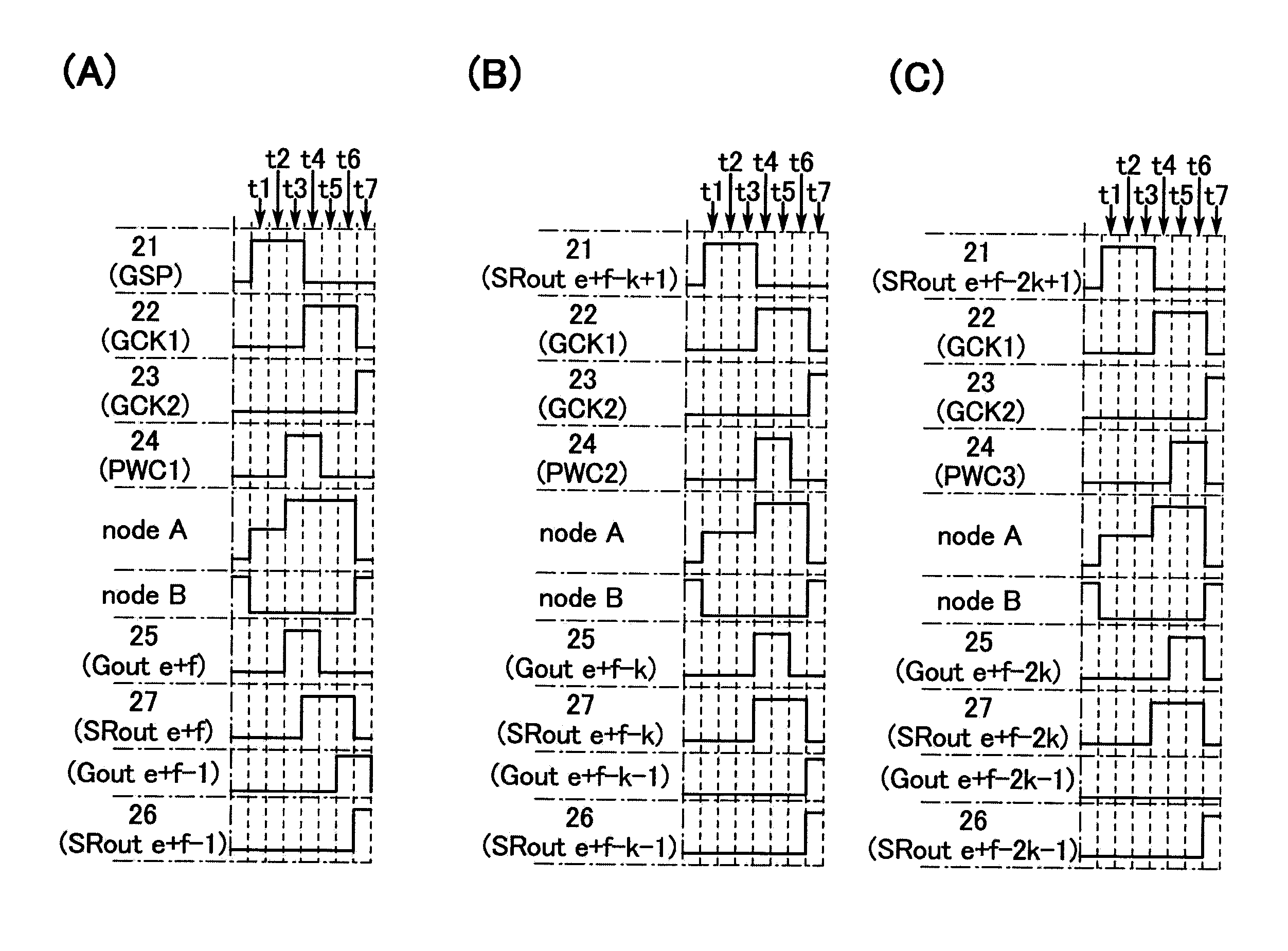
도 3(A)는 도 1에 나타낸 액정 표시 장치가 가지는 주사선 구동 회로(11e)의 구성예를 나타낸 도면이다. 또한, 본 실시형태에서는 주사선 구동 회로(11g)에는 주사선 구동 회로(11e)와 같은 구성의 주사선 구동 회로를 적용하는 것으로 하고, 상세한 설명을 생략한다. 도 3(A)에 나타낸 주사선 구동 회로(11e)는 제 1 주사선 구동 회로용 클록 신호(GCK1)를 공급하는 배선 내지 제 4 주사선 구동 회로용 클록 신호(GCK4)를 공급하는 배선과, 제 1 펄스폭 제어 신호(PWC1)를 공급하는 배선 내지 제 6 펄스폭 제어 신호(PWC6)를 공급하는 배선과, 1번째행에 배열된 주사선(13)에 전기적으로 접속된 제 1 펄스 출력 회로(20_1) 내지 e번째행에 배열된 주사선(13)에 전기적으로 접속된 제 e 펄스 출력 회로(20_e)를 가진다. 또한, 여기에서는 제 1 펄스 출력 회로(20_1)∼제 k 펄스 출력 회로(20_k)(k는 e/2 미만의 4의 배수)가 영역(101e)에 배열된 주사선(13)에 전기적으로 접속되고, 제 k+1 펄스 출력 회로(20_k+1)∼제 2k의 펄스 출력 회로(20_2k)가 영역(102e)에 배열된 주사선(13)에 전기적으로 접속되고, 제2k+1의 펄스 출력 회로(20_2k+1)∼제 e 펄스 출력 회로(20_e)가 영역(103e)에 배열된 주사선(13)에 전기적으로 접속되는 것으로 한다. 또한, 제 1 펄스 출력 회로(20_1) 내지 제 e 펄스 출력 회로(20_e)는 제 1 펄스 출력 회로(20_1)에 입력되는 주사선 구동 회로용 스타트 펄스(GSP)를 계기로 하여 시프트 기간마다 시프트 펄스를 순차 시프트하는 기능을 가진다. 또한, 제 1 펄스 출력 회로(20_1) 내지 제 e 펄스 출력 회로(20_e)에 있어서 복수의 시프트 펄스의 시프트를 병행하여 행하는 것이 가능하다. 즉, 제 1 펄스 출력 회로(20_1) 내지 제 e 펄스 출력 회로(20_e)에 있어서 시프트 펄스의 시프트가 행해지고 있는 기간내라고 하더라도, 제 1 펄스 출력 회로(20_1)에 주사선 구동 회로용 스타트 펄스(GSP)를 입력하는 것이 가능하다.Fig. 3 (A) is a diagram showing a configuration example of the scanning
도 3(B)는 상기 신호의 구체적인 파형의 일례를 나타낸 도면이다. 도 3(B)에 나타낸 제 1 주사선 구동 회로용 클록 신호(GCK1)는 주기적으로 하이 레벨의 전위(고전원 전위(Vdd))와 로 레벨의 전위(저전원 전위(Vss))를 반복하고, 듀티비가 1/4인 신호이다. 또한, 제 2 주사선 구동 회로용 클록 신호(GCK2)는 제 1 주사선 구동 회로용 클록 신호(GCK1)로부터 1/4 주기분 위상이 어긋난 신호이며, 제 3 주사선 구동 회로용 클록 신호(GCK3)는 제 1 주사선 구동 회로용 클록 신호(GCK1)로부터 1/2 주기분 위상이 어긋난 신호이며, 제 4 주사선 구동 회로용 클록 신호(GCK4)는 제 1 주사선 구동 회로용 클록 신호(GCK1)로부터 3/4 주기분 위상이 어긋난 신호이다. 제 1 펄스폭 제어 신호(PWC1)는 주기적으로 하이 레벨의 전위(고전원 전위(Vdd))와 로 레벨의 전위(저전원 전위(Vss))를 반복하고, 듀티비가 1/3인 신호이다. 또한, 제 2 펄스폭 제어 신호(PWC2)는 제 1 펄스폭 제어 신호(PWC1)로부터 1/6 주기분 위상이 어긋난 신호이며, 제 3 펄스폭 제어 신호(PWC3)는 제 1 펄스폭 제어 신호(PWC1)로부터 1/3 주기분 위상이 어긋난 신호이며, 제 4 펄스폭 제어 신호(PWC4)는 제 1 펄스폭 제어 신호(PWC1)로부터 1/2 주기분 위상이 어긋난 신호이며, 제 5 펄스폭 제어 신호(PWC5)는 제 1 펄스폭 제어 신호(PWC1)로부터 2/3 주기분 위상이 어긋난 신호이며, 제 6 펄스폭 제어 신호(PWC6)는 제 1 펄스폭 제어 신호(PWC1)로부터 5/6 주기분 위상이 어긋난 신호이다. 또한, 여기에서는 제 1 주사선 구동 회로용 클록 신호(GCK1) 내지 제 4 주사선 구동 회로용 클록 신호(GCK4)의 펄스폭과 제 1 펄스폭 제어 신호(PWC1) 내지 제 6 펄스폭 제어 신호(PWC6)의 펄스폭의 비는 3:2로 한다.3 (B) is a diagram showing an example of a specific waveform of the signal. The first scanning line drive circuit clock signal GCK1 shown in Fig. 3B periodically repeats a high level potential (high power supply potential Vdd) and a low level potential (low power supply potential Vss) And a duty ratio of 1/4. The second scanning line driving circuit clock signal GCK2 is a signal shifted in phase by 1/4 period from the first scanning line driving circuit clock signal GCK1 and the third scanning line driving circuit clock signal GCK3 is a And the fourth scanning line driving circuit clock signal GCK4 is a signal which is shifted from the first scanning line driving circuit clock signal GCK1 by a period of 3/4 cycle from the first scanning line driving circuit clock signal GCK1, Min. ≪ / RTI > The first pulse width control signal PWC1 periodically repeats a high level potential (high power supply potential Vdd) and a low level potential (low power supply potential Vss) and has a duty ratio of 1/3. The second pulse width control signal PWC2 is a signal whose phase is shifted by 1/6 period from the first pulse width control signal PWC1 and the third pulse width control signal PWC3 is a signal which is shifted by 1/6 period from the first pulse width control signal PWC1 The fourth pulse width control signal PWC4 is a signal whose phase is shifted by 1/2 cycle from the first pulse width control signal PWC1, The signal PWC5 is a signal shifted by 2/3 of the cycle from the first pulse width control signal PWC1 and the sixth pulse width control signal PWC6 is a signal which is shifted from the first pulse width control signal PWC1 by 5/6 Min. ≪ / RTI > Here, the pulse widths of the first scanning line driving circuit clock signal GCK1 to the fourth scanning line driving circuit clock signal GCK4 and the pulse widths of the first pulse width control signal PWC1 to the sixth pulse width control signal PWC6, Is 3: 2.
상술한 액정 표시 장치에 있어서는 제 1 펄스 출력 회로(20_1) 내지 제 e 펄스 출력 회로(20_e)로서, 동일한 구성을 가지는 회로를 적용할 수 있다. 단, 펄스 출력 회로가 가지는 복수의 단자의 전기적인 접속 관계는 펄스 출력 회로마다 다르다. 구체적인 접속 관계에 대하여 도 3(A), 도 3(C)를 참조하여 설명한다.In the liquid crystal display device described above, a circuit having the same configuration can be applied as the first pulse output circuit 20_1 to the eighth pulse output circuit 20_e. However, the electrical connection relationship of the plurality of terminals of the pulse output circuit differs from pulse output circuit to pulse output circuit. The concrete connection relationship will be described with reference to Figs. 3A and 3C.
제 1 펄스 출력 회로(20_1) 내지 제 e 펄스 출력 회로(20_e)의 각각은 단자(21)∼단자(27)를 가진다. 또한, 단자(21)∼단자(24) 및 단자(26)는 입력 단자이며, 단자(25) 및 단자(27)는 출력 단자이다.Each of the first pulse output circuit 20_1 to the eighth pulse output circuit 20_e has a terminal 21 to a terminal 27. [ The
먼저, 단자(21)에 대하여 설명한다. 제 1 펄스 출력 회로(20_1)의 단자(21)는 주사선 구동 회로용 스타트 펄스(GSP)를 공급하는 배선에 전기적으로 접속되고, 제 2 펄스 출력 회로(20_2)∼제 e 펄스 출력 회로(20_e)의 단자(21)는 전단의 펄스 출력 회로의 단자(27)에 전기적으로 접속된다.First, the terminal 21 will be described. The terminal 21 of the first pulse output circuit 20_1 is electrically connected to the wiring for supplying the scanning line driving circuit start pulse GSP and the second pulse output circuit 20_2 to the e pulse output circuit 20_e, The
다음에, 단자(22)에 대하여 설명한다. 제 (e+f+4-4a)의 펄스 출력 회로(a는 e/4 이하의 자연수)의 단자(22)는 제 1 주사선 구동 회로용 클록 신호(GCK1)를 공급하는 배선에 전기적으로 접속되고, 제 (e+f+3-4a)의 펄스 출력 회로의 단자(22)는 제 2 주사선 구동 회로용 클록 신호(GCK2)를 공급하는 배선에 전기적으로 접속되고, 제 (e+f+2-4a)의 펄스 출력 회로의 단자(22)는 제 3 주사선 구동 회로용 클록 신호(GCK3)를 공급하는 배선에 전기적으로 접속되고, 제 (e+f+1-4a)의 펄스 출력 회로의 단자(22)는 제 4 주사선 구동 회로용 클록 신호(GCK4)를 공급하는 배선에 전기적으로 접속된다.Next, the terminal 22 will be described. The terminal 22 of the pulse output circuit (a is a natural number equal to or smaller than e / 4) of the (e + f + 4-4a) is electrically connected to the wiring for supplying the clock signal GCK1 for the first scanning line driving circuit, The
다음에, 단자(23)에 대하여 설명한다. 제 (e+f+4-4a)의 펄스 출력 회로의 단자(23)는 제 2 주사선 구동 회로용 클록 신호(GCK2)를 공급하는 배선에 전기적으로 접속되고, 제 (e+f+3-4a)의 펄스 출력 회로의 단자(23)는 제 3 주사선 구동 회로용 클록 신호(GCK3)를 공급하는 배선에 전기적으로 접속되고, 제 (e+f+2-4a)의 펄스 출력 회로의 단자(23)는 제 4 주사선 구동 회로용 클록 신호(GCK4)를 공급하는 배선에 전기적으로 접속되고, 제 (e+f+1-4a)의 펄스 출력 회로의 단자(23)는 제 1 주사선 구동 회로용 클록 신호(GCK1)를 공급하는 배선에 전기적으로 접속된다.Next, the terminal 23 will be described. The terminal 23 of the pulse output circuit of the (e + f + 4-4a) is electrically connected to the wiring for supplying the second scanning line driving circuit clock signal GCK2 and is connected to the terminal (e + f + 3-4a) 23) is electrically connected to the wiring for supplying the third scanning line driving circuit clock signal GCK3 and the
다음에, 단자(24)에 대하여 설명한다. 제 (2b-1)의 펄스 출력 회로(b는 k/2 이하의 자연수)의 단자(24)는 제 1 펄스폭 제어 신호(PWC1)를 공급하는 배선에 전기적으로 접속되고, 제 2b 펄스 출력 회로의 단자(24)는 제 4 펄스폭 제어 신호(PWC4)를 공급하는 배선에 전기적으로 접속되고, 제 (2c-1)의 펄스 출력 회로(c는 (k/2+1) 이상 k 이하의 자연수)의 단자(24)는 제 2 펄스폭 제어 신호(PWC2)를 공급하는 배선에 전기적으로 접속되고, 제 2c 펄스 출력 회로의 단자(24)는 제 5 펄스폭 제어 신호(PWC5)를 공급하는 배선에 전기적으로 접속되고, 제 (2d-1)의 펄스 출력 회로(d는 (k+1) 이상 e/2 이하의 자연수)의 단자(24)는 제 3 펄스폭 제어 신호(PWC3)를 공급하는 배선에 전기적으로 접속되고, 제 2d 펄스 출력 회로의 단자(24)는 제 6 펄스폭 제어 신호(PWC6)를 공급하는 배선에 전기적으로 접속된다.Next, the terminal 24 will be described. The terminal 24 of the (2b-1) pulse output circuit (b is a natural number equal to or smaller than k / 2) is electrically connected to the wiring for supplying the first pulse width control signal PWC1, The
다음에, 단자(25)에 대하여 설명한다. 제 x 펄스 출력 회로(x는 e 이하의 자연수)의 단자(25)는 x번째행에 배열된 주사선(13_x)에 전기적으로 접속된다.Next, the terminal 25 will be described. The
다음에, 단자(26)에 대하여 설명한다. 제 y 펄스 출력 회로(y는 e-1 이하의 자연수)의 단자(26)는 제 (y+1)의 펄스 출력 회로의 단자(27)에 전기적으로 접속되고, 제 e 펄스 출력 회로의 단자(26)는 제 e 펄스 출력 회로용 스톱 신호(STP)를 공급하는 배선에 전기적으로 접속된다. 또한, 제 e 펄스 출력 회로용 스톱 신호(STP)는 만약 제 (e+1)의 펄스 출력 회로가 설치되어 있다면, 이 제 (e+1)의 펄스 출력 회로의 단자(27)로부터 출력되는 신호에 상당하는 신호이다. 구체적으로는 이들 신호는 실제로 더미 회로로서 제 (e+1)의 펄스 출력 회로를 형성하는 것, 또는 외부로부터 이 신호를 직접 입력하는 것 등에 의해 제 e 펄스 출력 회로에 공급할 수 있다.Next, the terminal 26 will be described. The terminal 26 of the y-th pulse output circuit (y is a natural number equal to or smaller than e-1) is electrically connected to the
각 펄스 출력 회로의 단자(27)의 접속 관계는 이미 설명되어있다. 따라서, 여기에서는 상술한 설명을 원용하기로 한다.The connection relationship of the
<주사선 구동 회로(11f)의 구성예>≪ Example of the configuration of the scanning
도 4(A)는 도 1에 나타낸 액정 표시 장치가 가지는 주사선 구동 회로(11f)의 구성예를 나타낸 도면이다. 도 4(A)에 나타낸 주사선 구동 회로(11f)는 e+f번째행의 주사선(13_e+f)으로부터 e+1번째행의 주사선(13_e+1)을 향하는 순번으로, 각 주사선을 통하여 화소에 선택 신호를 출력하도록, 도 3(A)에 나타낸 주사선 구동 회로(11e)를 반전한 구성을 구비한다.Fig. 4 (A) is a diagram showing a configuration example of the scanning
도 4(A)에 나타낸 주사선 구동 회로(11f)는 제 1 주사선 구동 회로용 클록 신호(GCK1)를 공급하는 배선 내지 제 4 주사선 구동 회로용 클록 신호(GCK4)를 공급하는 배선과, 제 1 펄스폭 제어 신호(PWC1)를 공급하는 배선 내지 제 6의 펄스폭 제어 신호(PWC6)를 공급하는 배선과, e+1번째행에 배열된 주사선(13)에 전기적으로 접속된 제 e+1의 펄스 출력 회로(20_e+1), 내지 e+f번째행에 배열된 주사선(13)에 전기적으로 접속된 제 e+f의 펄스 출력 회로(20_e+f)를 가진다. 또한, 여기에서는 제 e+1의 펄스 출력 회로(20_e+1)∼제 e+f-2k(k는 f/2 미만의 4의 배수)의 펄스 출력 회로(20_e+f-2k)가 영역(101f)에 배열된 주사선(13)에 전기적으로 접속되고, 제 e+f-2k+1의 펄스 출력 회로(20_e+f-2k+1)∼제 e+f-k의 펄스 출력 회로(20_e+f-k)가, 영역(102f)에 배열된 주사선(13)에 전기적으로 접속되고, 제 e+f-k+1의 펄스 출력 회로(20_e+f-k+1)∼제 e+f의 펄스 출력 회로(20_e+f)가, 영역(103f)에 배열된 주사선(13)에 전기적으로 접속되는 것으로 한다. 또한, 제 e+1의 펄스 출력 회로(20_e+1) 내지 제 e+f의 펄스 출력 회로(20_e+f)는 제 e+f의 펄스 출력 회로(20_e+f)에 입력되는 주사선 구동 회로용 스타트 펄스(GSP)를 계기로 하여 시프트 기간마다 시프트 펄스를 순차 시프트하는 기능을 가진다. 또한, 제 e+1의 펄스 출력 회로(20_e+1) 내지 제 e+f의 펄스 출력 회로(20_e+f)에 있어서 복수의 시프트 펄스의 시프트를 병행하여 행하는 것이 가능하다. 즉, 제 e+1의 펄스 출력 회로(20_e+1) 내지 제 e+f의 펄스 출력 회로(20_e+f)에 있어서 시프트 펄스의 시프트가 행해지고 있는 기간내라고 하더라도, 제 e+f의 펄스 출력 회로(20_e+f)에 주사선 구동 회로용 스타트 펄스(GSP)를 입력하는 것이 가능하다.The scanning
도 4(B)는 상기 신호의 구체적인 파형의 일례를 나타낸 도면이다. 도 4(B)에 나타낸 제 1 주사선 구동 회로용 클록 신호(GCK1)는 주기적으로 하이 레벨의 전위(고전원 전위(Vdd))와 로 레벨의 전위(저전원 전위(Vss))를 반복하고, 듀티비가 1/4인 신호이다. 또한, 제 2 주사선 구동 회로용 클록 신호(GCK2)는 제 1 주사선 구동 회로용 클록 신호(GCK1)로부터 1/4 주기분 위상이 어긋난 신호이며, 제 3 주사선 구동 회로용 클록 신호(GCK3)는 제 1 주사선 구동 회로용 클록 신호(GCK1)로부터 1/2 주기분 위상이 어긋난 신호이며, 제 4 주사선 구동 회로용 클록 신호(GCK4)는 제 1 주사선 구동 회로용 클록 신호(GCK1)로부터 3/4 주기분 위상이 어긋난 신호이다. 제 1 펄스폭 제어 신호(PWC1)는 주기적으로 하이 레벨의 전위(고전원 전위(Vdd))와 로 레벨의 전위(저전원 전위(Vss))를 반복하고, 듀티비가 1/3인 신호이다. 또한, 제 2 펄스폭 제어 신호(PWC2)는 제 1 펄스폭 제어 신호(PWC1)로부터 1/6 주기분 위상이 어긋난 신호이며, 제 3 펄스폭 제어 신호(PWC3)는 제 1 펄스폭 제어 신호(PWC1)로부터 1/3 주기분 위상이 어긋난 신호이며, 제 4 펄스폭 제어 신호(PWC4)는 제 1 펄스폭 제어 신호(PWC1)로부터 1/2 주기분 위상이 어긋난 신호이며, 제 5 펄스폭 제어 신호(PWC5)는 제 1 펄스폭 제어 신호(PWC1)로부터 2/3 주기분 위상이 어긋난 신호이며, 제 6 펄스폭 제어 신호(PWC6)는 제 1 펄스폭 제어 신호(PWC1)로부터 5/6 주기분 위상이 어긋난 신호이다. 또한, 여기에서는 제 1 주사선 구동 회로용 클록 신호(GCK1) 내지 제 4 주사선 구동 회로용 클록 신호(GCK4)의 펄스폭과 제 1 펄스폭 제어 신호(PWC1) 내지 제 6 펄스폭 제어 신호(PWC6)의 펄스폭의 비는 3:2로 한다.4 (B) is a diagram showing an example of a specific waveform of the above-mentioned signal. The first scanning line drive circuit clock signal GCK1 shown in Fig. 4B periodically repeats a high level potential (high power supply potential Vdd) and a low level potential (low power supply potential Vss) And a duty ratio of 1/4. The second scanning line driving circuit clock signal GCK2 is a signal shifted in phase by 1/4 period from the first scanning line driving circuit clock signal GCK1 and the third scanning line driving circuit clock signal GCK3 is a And the fourth scanning line driving circuit clock signal GCK4 is a signal which is shifted from the first scanning line driving circuit clock signal GCK1 by a period of 3/4 cycle from the first scanning line driving circuit clock signal GCK1, Min. ≪ / RTI > The first pulse width control signal PWC1 periodically repeats a high level potential (high power supply potential Vdd) and a low level potential (low power supply potential Vss) and has a duty ratio of 1/3. The second pulse width control signal PWC2 is a signal whose phase is shifted by 1/6 period from the first pulse width control signal PWC1 and the third pulse width control signal PWC3 is a signal which is shifted by 1/6 period from the first pulse width control signal PWC1 The fourth pulse width control signal PWC4 is a signal whose phase is shifted by 1/2 cycle from the first pulse width control signal PWC1, The signal PWC5 is a signal shifted by 2/3 of the cycle from the first pulse width control signal PWC1 and the sixth pulse width control signal PWC6 is a signal which is shifted from the first pulse width control signal PWC1 by 5/6 Min. ≪ / RTI > Here, the pulse widths of the first scanning line driving circuit clock signal GCK1 to the fourth scanning line driving circuit clock signal GCK4 and the pulse widths of the first pulse width control signal PWC1 to the sixth pulse width control signal PWC6, Is 3: 2.
상술한 액정 표시 장치에서는 제 e+1의 펄스 출력 회로(20_e+1) 내지 제 e+f의 펄스 출력 회로(20_e+f)로서, 동일한 구성을 가지는 회로를 적용할 수 있다. 단, 펄스 출력 회로가 가지는 복수의 단자의 전기적인 접속 관계는 펄스 출력 회로마다 다르다. 구체적인 접속 관계에 대하여 도 4(A), 도 4(C)를 참조하여 설명한다.In the above-described liquid crystal display device, a circuit having the same configuration can be applied as the (e + 1) th pulse output circuit 20_e + 1 to the (e + f) th pulse output circuit 20_e + f. However, the electrical connection relationship of the plurality of terminals of the pulse output circuit differs from pulse output circuit to pulse output circuit. A concrete connection relationship will be described with reference to Figs. 4 (A) and 4 (C).
제 e+1의 펄스 출력 회로(20_e+1) 내지 제 e+f의 펄스 출력 회로(20_e+f)의 각각은 단자(21)∼단자(27)를 가진다. 또한, 단자(21)∼단자(24) 및 단자(26)는 입력 단자이며, 단자(25) 및 단자(27)는 출력 단자이다.Each of the pulse output circuits 20_e + 1 to e + f of the (e + 1) th pulse output circuit 20_e + f has a terminal 21 to a terminal 27. The
먼저, 단자(21)에 대하여 설명한다. 제 e+f의 펄스 출력 회로(20_e+f)의 단자(21)는 주사선 구동 회로용 스타트 펄스(GSP)를 공급하는 배선에 전기적으로 접속되고, 제 e+1의 펄스 출력 회로(20_e+1)∼제 e+f-1의 펄스 출력 회로(20_e+f-1)의 단자(21)는 전단의 펄스 출력 회로의 단자(27)에 전기적으로 접속된다. 또한, 전단의 펄스 출력 회로는 직전에 동작하는 펄스 출력 회로를 가리키고, 그 배열되는 위치에 직접 관련지을 수 없다.First, the terminal 21 will be described. The terminal 21 of the pulse output circuit 20_e + f of the (e + f) th column is electrically connected to the wiring for supplying the scanning line driving start pulse GSP, and the pulse of the pulse output circuit 20_e + The terminal 21 of the output circuit 20_e + f-1 is electrically connected to the
다음에, 단자(22)에 대하여 설명한다. 제 (e+f+4-4a)의 펄스 출력 회로(a는 e/4 이하의 자연수)의 단자(22)는 제 1 주사선 구동 회로용 클록 신호(GCK1)를 공급하는 배선에 전기적으로 접속되고, 제 (e+f+3-4a)의 펄스 출력 회로의 단자(22)는 제 2 주사선 구동 회로용 클록 신호(GCK2)를 공급하는 배선에 전기적으로 접속되고, 제 (e+f+2-4a)의 펄스 출력 회로의 단자(22)는 제 3 주사선 구동 회로용 클록 신호(GCK3)를 공급하는 배선에 전기적으로 접속되고, 제 (e+f+1-4a)의 펄스 출력 회로의 단자(22)는 제 4 주사선 구동 회로용 클록 신호(GCK4)를 공급하는 배선에 전기적으로 접속된다.Next, the terminal 22 will be described. The terminal 22 of the pulse output circuit (a is a natural number equal to or smaller than e / 4) of the (e + f + 4-4a) is electrically connected to the wiring for supplying the clock signal GCK1 for the first scanning line driving circuit, The
다음에, 단자(23)에 대하여 설명한다. 제 (e+f+4-4a)의 펄스 출력 회로의 단자(23)는 제 2 주사선 구동 회로용 클록 신호(GCK2)를 공급하는 배선에 전기적으로 접속되고, 제 (e+f+3-4a)의 펄스 출력 회로의 단자(23)는 제 3 주사선 구동 회로용 클록 신호(GCK3)를 공급하는 배선에 전기적으로 접속되고, 제 (e+f+2-4a)의 펄스 출력 회로의 단자(23)는 제 4 주사선 구동 회로용 클록 신호(GCK4)를 공급하는 배선에 전기적으로 접속되고, 제 (e+f+1-4a)의 펄스 출력 회로의 단자(23)는 제 1 주사선 구동 회로용 클록 신호(GCK1)를 공급하는 배선에 전기적으로 접속된다.Next, the terminal 23 will be described. The terminal 23 of the pulse output circuit of the (e + f + 4-4a) is electrically connected to the wiring for supplying the second scanning line driving circuit clock signal GCK2 and is connected to the terminal (e + f + 3-4a) 23) is electrically connected to the wiring for supplying the third scanning line driving circuit clock signal GCK3 and the
다음에, 단자(24)에 대하여 설명한다. 제 (2b-1)의 펄스 출력 회로(b는 k/2 이하의 자연수)의 단자(24)는 제 1 펄스폭 제어 신호(PWC1)를 공급하는 배선에 전기적으로 접속되고, 제 2b 펄스 출력 회로의 단자(24)는 제 4 펄스폭 제어 신호(PWC4)를 공급하는 배선에 전기적으로 접속되고, 제 (2c-1)의 펄스 출력 회로(c는 (k/2+1) 이상 k 이하의 자연수)의 단자(24)는 제 2 펄스폭 제어 신호(PWC2)를 공급하는 배선에 전기적으로 접속되고, 제 2c의 펄스 출력 회로의 단자(24)는 제 5 펄스폭 제어 신호(PWC5)를 공급하는 배선에 전기적으로 접속되고, 제 (2d-1) 펄스 출력 회로(d는 (k+1) 이상 e/2 이하의 자연수)의 단자(24)는 제 3 펄스폭 제어 신호(PWC3)를 공급하는 배선에 전기적으로 접속되고, 제 2d 펄스 출력 회로의 단자(24)는 제 6 펄스폭 제어 신호(PWC6)를 공급하는 배선에 전기적으로 접속된다.Next, the terminal 24 will be described. The terminal 24 of the (2b-1) pulse output circuit (b is a natural number equal to or smaller than k / 2) is electrically connected to the wiring for supplying the first pulse width control signal PWC1, The
다음에, 단자(25)에 대하여 설명한다. 제 x 펄스 출력 회로(x는 e+1 이상 e+f 이하의 자연수)의 단자(25)는 x번째행에 배열된 주사선(13_x)에 전기적으로 접속된다.Next, the terminal 25 will be described. The
다음에, 단자(26)에 대하여 설명한다. 제 y 펄스 출력 회로(y는 e-1 이하의 자연수)의 단자(26)는 제 (y-1)의 펄스 출력 회로의 단자(27)에 전기적으로 접속되고, 제 e+1의 펄스 출력 회로의 단자(26)는 제 e+1의 펄스 출력 회로용 스톱 신호(STP)를 공급하는 배선에 전기적으로 접속된다. 또한, 제 e+1의 펄스 출력 회로용 스톱 신호(STP)는 주사선 구동 회로(11e)가 구비하는 펄스 출력 회로(20_e)와는 별도로 주사선 구동 회로(11f)에 더미 회로로서 제 e 펄스 출력 회로를 형성하는 것, 또는 외부로부터 이 신호를 직접 입력하는 것 등에 의해 제 e+1의 펄스 출력 회로에 공급할 수 있다.Next, the terminal 26 will be described. The terminal 26 of the y-th pulse output circuit (y is a natural number equal to or smaller than e-1) is electrically connected to the
각 펄스 출력 회로의 단자(27)의 접속 관계는 이미 설멸되어 있다. 따라서, 여기에서는 상술한 설명을 원용하는 것으로 한다.The connection relationship of the
<펄스 출력 회로의 구성예><Configuration Example of Pulse Output Circuit>
도 5(A)는 도 3(A), 도 3(C), 및 도 4(A), 도 4(C)에 나타낸 펄스 출력 회로의 구성예를 나타낸 도면이다. 도 5(A)에 나타낸 펄스 출력 회로는 트랜지스터(31) 내지 트랜지스터(39)를 가진다.Fig. 5A is a diagram showing a configuration example of the pulse output circuit shown in Figs. 3 (A), 3 (C), 4 (A) and 4 (C). The pulse output circuit shown in Fig. 5 (A) has a
트랜지스터(31)는 소스 및 드레인의 한쪽이 고전원 전위(Vdd)를 공급하는 배선(이하, 고전원 전위선이라고도 함)에 전기적으로 접속되고, 게이트가 단자(21)에 전기적으로 접속된다.One of the source and the drain of the
트랜지스터(32)는 소스 및 드레인의 한쪽이 저전원 전위(Vss)를 공급하는 배선(이하, 저전원 전위선이라고도 함)에 전기적으로 접속되고, 소스 및 드레인의 다른 한쪽이 트랜지스터(31)의 소스 및 드레인의 다른 한쪽에 전기적으로 접속된다.One of the source and the drain of the
트랜지스터(33)는 소스 및 드레인의 한쪽이 단자(22)에 전기적으로 접속되고, 소스 및 드레인의 다른 한쪽이 단자(27)에 전기적으로 접속되고, 게이트가 트랜지스터(31)의 소스 및 드레인의 다른 한쪽 및 트랜지스터(32)의 소스 및 드레인의 다른 한쪽에 전기적으로 접속된다.One of the source and the drain of the
트랜지스터(34)는 소스 및 드레인의 한쪽이 저전원 전위선에 전기적으로 접속되고, 소스 및 드레인의 다른 한쪽이 단자(27)에 전기적으로 접속되고, 게이트가 트랜지스터(32)의 게이트에 전기적으로 접속된다.One of the source and the drain of the
트랜지스터(35)는 소스 및 드레인의 한쪽이 저전원 전위선에 전기적으로 접속되고, 소스 및 드레인의 다른 한쪽이 트랜지스터(32)의 게이트 및 트랜지스터(34)의 게이트에 전기적으로 접속되고, 게이트가 단자(21)에 전기적으로 접속된다.One of the source and the drain of the
트랜지스터(36)는 소스 및 드레인의 한쪽이 고전원 전위선에 전기적으로 접속되고, 소스 및 드레인의 다른 한쪽이 트랜지스터(32)의 게이트, 트랜지스터(34)의 게이트, 및 트랜지스터(35)의 소스 및 드레인의 다른 한쪽에 전기적으로 접속되고, 게이트가 단자(26)에 전기적으로 접속된다. 또한, 트랜지스터(36)의 소스 및 드레인의 한쪽이, 저전원 전위(Vss)보다 고전위이며 또한 고전원 전위(Vdd)보다 저전위인 전원 전위(Vcc)를 공급하는 배선에 전기적으로 접속되는 구성으로 할 수도 있다.One of the source and the drain of the
트랜지스터(37)는 소스 및 드레인의 한쪽이 고전원 전위선에 전기적으로 접속되고, 소스 및 드레인의 다른 한쪽이 트랜지스터(32)의 게이트, 트랜지스터(34)의 게이트, 트랜지스터(35)의 소스 및 드레인의 다른 한쪽, 및 트랜지스터(36)의 소스 및 드레인의 다른 한쪽에 전기적으로 접속되고, 게이트가 단자(23)에 전기적으로 접속된다. 또한, 트랜지스터(37)의 소스 및 드레인의 한쪽이, 전원 전위(Vcc)를 공급하는 배선에 전기적으로 접속되는 구성으로 할 수도 있다.One of the source and the drain of the
트랜지스터(38)는 소스 및 드레인의 한쪽이 단자(24)에 전기적으로 접속되고, 소스 및 드레인의 다른 한쪽이 단자(25)에 전기적으로 접속되고, 게이트가 트랜지스터(31)의 소스 및 드레인의 다른 한쪽, 트랜지스터(32)의 소스 및 드레인의 다른 한쪽, 및 트랜지스터(33)의 게이트에 전기적으로 접속된다.One of the source and the drain of the
트랜지스터(39)는 소스 및 드레인의 한쪽이 저전원 전위선에 전기적으로 접속되고, 소스 및 드레인의 다른 한쪽이 단자(25)에 전기적으로 접속되고, 게이트가 트랜지스터(32)의 게이트, 트랜지스터(34)의 게이트, 트랜지스터(35)의 소스 및 드레인의 다른 한쪽, 트랜지스터(36)의 소스 및 드레인의 다른 한쪽, 및 트랜지스터(37)의 소스 및 드레인의 다른 한쪽에 전기적으로 접속된다.One of the source and the drain of the
또한, 이하에서는 트랜지스터(31)의 소스 및 드레인의 다른 한쪽, 트랜지스터(32)의 소스 및 드레인의 다른 한쪽, 트랜지스터(33)의 게이트, 및 트랜지스터(38)의 게이트가 전기적으로 접속하는 노드를 노드(A)로 하고, 트랜지스터(32)의 게이트, 트랜지스터(34)의 게이트, 트랜지스터(35)의 소스 및 드레인의 다른 한쪽, 트랜지스터(36)의 소스 및 드레인의 다른 한쪽, 트랜지스터(37)의 소스 및 드레인의 다른 한쪽, 및 트랜지스터(39)의 게이트가 전기적으로 접속하는 노드를 노드(B)로 하여 설명한다.A node to which the other of the source and the drain of the
<펄스 출력 회로의 동작예><Operation example of pulse output circuit>
도 5(B)∼도 5(D), 도 6(A)∼도 6(C), 및 도 7(A)∼도 7(C)를 참조하여, 상술한 펄스 출력 회로의 동작에 대하여 설명한다. 구체적으로는 주사선 구동 회로(11e)의 제 1 펄스 출력 회로(20_1)의 단자(21), 주사선 구동 회로(11f)의 제 1 펄스 출력 회로(20_e+f)의 단자(21), 및 주사선 구동 회로(11g)의 제 1 펄스 출력 회로(20_e+f+1)의 단자(21)에 타이밍을 제어하여 주사선 구동 회로용 스타트 펄스(GSP)를 입력하는 경우의 동작예를 설명한다. 스타트 펄스(GSP)를 입력하는 타이밍을 제어함으로써, 제 1 펄스 출력 회로(20_1), 제 (k+1)의 펄스 출력 회로(20_k+1), 및 제 (2k+1)의 펄스 출력 회로(20_2k+1)의 단자(27)로부터 동일 타이밍에서 시프트 펄스를 출력하고, 또한 제 e+f의 펄스 출력 회로(20_e+f), 제 (e+f-k) 펄스 출력 회로(20_e+f-k), 제 (e+f-2k) 펄스 출력 회로(20_e+f-2k)의 단자(27)로부터 동일 타이밍에서 시프트 펄스를 출력하고, 또한, 제 e+f+1의 펄스 출력 회로(20_e+f+1), 제 (e+f+k+1)의 펄스 출력 회로(20_e+f+k+1), 및 제 (e+f+2k+1)의 펄스 출력 회로(20_e+f+2k+1)의 단자(27)로부터 동일 타이밍에서 시프트 펄스를 출력할 수 있다.The operation of the pulse output circuit described above will be described with reference to Figs. 5 (B) to 5 (D), 6 (A) to 6 (C), and 7 do. Concretely, the
주사선 구동 회로(11e)의 동작에 대하여 설명한다. 구체적으로는 도 5(B)는 주사선 구동 회로용 스타트 펄스(GSP)가 입력될 때의 제 1 펄스 출력 회로(20_1)의 각 단자에 입력되는 신호의 전위, 및 노드(A) 및 노드(B)의 전위를 나타내고 있고, 도 5(C)는 제 k 펄스 출력 회로(20_k)로부터 하이 레벨의 전위가 입력될 때의 제 (k+1)의 펄스 출력 회로(20_k+1)의 각 단자에 입력되는 신호의 전위, 및 노드(A) 및 노드(B)의 전위를 나타내고 있고, 도 5(D)는 제 2k의 펄스 출력 회로(20_2k)로부터 하이 레벨의 전위가 입력될 때의 제 (2k+1)의 펄스 출력 회로(20_2k+1)의 각 단자에 입력되는 신호의 전위, 및 노드(A) 및 노드(B)의 전위를 나타내고 있다.The operation of the scanning
또한, 도 5(B)∼도 5(D)에서는 각 단자에 입력되는 신호를 괄호 안에 부기하고 있다. 또한, 각각의 후단에 배열되는 펄스 출력 회로(제 2 펄스 출력 회로(20_2), 제 (k+2)의 펄스 출력 회로(20_k+2), 제 (2k+2)의 펄스 출력 회로(20_2k+2))의 단자(25)로부터 출력되는 신호(Gout2, Goutk+2, Gout2k+2) 및 단자(27)의 출력 신호(SRout2 = 제 1 펄스 출력 회로(20_1)의 단자(26)의 입력 신호, SRoutk+2 = 제 (k+1)의 펄스 출력 회로(20_k+1)의 단자(26)의 입력 신호, SRout2k+2= 제 (2k+1)의 펄스 출력 회로(20_2k+1)의 단자(26)의 입력 신호)도 부기하고 있다. 또한, 도면 중에서, Gout는 펄스 출력 회로의 주사선에 대한 출력 신호를 나타내고, SRout는 이 펄스 출력 회로의, 후단의 펄스 출력 회로에 대한 출력 신호를 나타내고 있다.5 (B) to 5 (D), signals input to the respective terminals are enclosed in parentheses. The
먼저, 도 5(B)를 참조하여, 제 1 펄스 출력 회로(20_1)에 주사선 구동 회로용 스타트 펄스(GSP)로서 하이 레벨의 전위가 입력되는 경우에 대하여 설명한다.First, referring to Fig. 5 (B), a case where a high level potential is inputted as the scanning line driving circuit start pulse GSP to the first pulse output circuit 20_1 will be described.
기간(t1)에 있어서, 단자(21)에 하이 레벨의 전위(고전원 전위(Vdd))가 입력된다. 이것에 의해, 트랜지스터(31, 35)가 온 상태가 된다. 따라서, 노드(A)의 전위가 하이 레벨의 전위(고전원 전위(Vdd)로부터 트랜지스터(31)의 스레시홀드 전압분 하강한 전위)로 상승하고, 또한 노드(B)의 전위가 저전원 전위(Vss)로 하강한다. 이것에 부수하여, 트랜지스터(33, 38)가 온 상태가 되고, 트랜지스터(32, 34, 39)가 오프 상태가 된다. 이상에 의해, 기간(t1)에서, 단자(27)로부터 출력되는 신호는 단자(22)에 입력되는 신호가 되고, 단자(25)로부터 출력되는 신호는 단자(24)에 입력되는 신호가 된다. 여기서, 기간(t1)에 있어서, 단자(22) 및 단자(24)에 입력되는 신호는 모두 로 레벨의 전위(저전원 전위(Vss))이다. 따라서, 기간(t1)에서, 제 1 펄스 출력 회로(20_1)는 제 2 펄스 출력 회로(20_2)의 단자(21), 및 화소부에 있어서 1번째행에 배열된 주사선에 로 레벨의 전위(저전원 전위(Vss))를 출력한다.In the period t1, a high level potential (high power supply potential Vdd) is input to the terminal 21. As a result, the
기간(t2)에 있어서, 각 단자에 입력되는 신호는 기간(t1)과 변화가 없다. 따라서, 단자(25) 및 단자(27)로부터 출력되는 신호도 변화하지 않고, 모두 로 레벨의 전위(저전원 전위(Vss))를 출력한다.In the period t2, the signal input to each terminal does not change from the period t1. Therefore, the signal output from the terminal 25 and the terminal 27 does not change, and outputs a low level potential (low power supply potential Vss).
기간(t3)에 있어서, 단자(24)에 하이 레벨의 전위(고전원 전위(Vdd))가 입력된다. 또한, 노드(A)의 전위(트랜지스터(31)의 소스의 전위)는 기간(t1)에 있어서 하이 레벨의 전위(고전원 전위(Vdd)로부터 트랜지스터(31)의 스레시홀드 전압분 하강한 전위)까지 상승한다. 따라서, 트랜지스터(31)는 오프 상태로 되어 있다. 이 때, 단자(24)에 하이 레벨의 전위(고전원 전위(Vdd))가 입력됨으로써, 트랜지스터(38)의 소스와 게이트의 용량 결합에 의해, 노드(A)의 전위(트랜지스터(38)의 게이트의 전위)가 더욱 상승한다(부트스트랩 동작). 또한, 이 부트스트랩 동작을 행하는 것에 의해, 단자(25)로부터 출력되는 신호가 단자(24)에 입력되는 하이 레벨의 전위(고전원 전위(Vdd))로부터 하강하는 일이 없다. 따라서, 기간(t3)에 있어서, 제 1 펄스 출력 회로(20_1)는 화소부에 있어서 1번째행에 배열된 주사선에 하이 레벨의 전위(고전원 전위(Vdd) = 선택 신호)를 출력한다.During the period t3, a high level potential (high power supply potential Vdd) is input to the terminal 24. [ The potential of the node A (the potential of the source of the transistor 31) is higher than the potential at the high level (high potential level Vdd) by the threshold voltage of the
기간(t4)에 있어서, 단자(22)에 하이 레벨의 전위(고전원 전위(Vdd))가 입력된다. 여기서, 노드(A)의 전위는 부트스트랩 동작에 의해 상승하기 때문에, 단자(27)로부터 출력되는 신호가 단자(22)에 입력되는 하이 레벨의 전위(고전원 전위(Vdd))로부터 하강하는 일이 없다. 따라서, 기간(t4)에 있어서, 단자(27)로부터는 단자(22)에 입력되는 하이 레벨의 전위(고전원 전위(Vdd))가 출력된다. 즉, 제 1 펄스 출력 회로(20_1)는 제 2 펄스 출력 회로(20_2)의 단자(21)에 하이 레벨의 전위(고전원 전위(Vdd) = 시프트 펄스)를 출력한다. 또한, 기간(t4)에 있어서, 단자(24)에 입력되는 신호는 하이 레벨의 전위(고전원 전위(Vdd))를 유지하기 때문에, 제 1 펄스 출력 회로(20_1)로부터 화소부에 있어서 1번째행에 배열된 주사선에 대하여 출력되는 신호는 하이 레벨의 전위(고전원 전위(Vdd) = 선택 신호)인 채이다. 또한, 기간(t4)에서의 이 펄스 출력 회로의 출력 신호에는 직접 관여하지 않지만, 단자(21)에 로 레벨의 전위(저전원 전위(Vss))가 입력되기 때문에 트랜지스터(35)는 오프 상태가 된다.In the period t4, a high level potential (high power supply potential Vdd) is input to the terminal 22. Here, since the potential of the node A rises by the bootstrap operation, the signal output from the terminal 27 falls from the high level potential (high power supply potential Vdd) input to the terminal 22 There is no. Therefore, the high-level potential (high power supply potential Vdd) input to the terminal 22 is outputted from the terminal 27 during the period t4. That is, the first pulse output circuit 20_1 outputs a high level potential (high power supply potential (Vdd) = shift pulse) to the
기간(t5)에 있어서, 단자(24)에 로 레벨의 전위(저전원 전위(Vss))가 입력된다. 여기서, 트랜지스터(38)는 온 상태를 유지한다. 따라서, 기간(t5)에 있어서, 제 1 펄스 출력 회로(20_1)로부터 화소부에 있어서 1번째행에 배열된 주사선에 대하여 출력되는 신호는 로 레벨의 전위(저전원 전위(Vss))가 된다.In the period t5, a low level potential (low power supply potential Vss) is input to the terminal 24. [ Here, the
기간(t6)에 있어서, 각 단자에 입력되는 신호는 기간(t5)과 변화가 없다. 따라서, 단자(25) 및 단자(27)로부터 출력되는 신호도 변화하지 않고, 단자(25)로부터는 로 레벨의 전위(저전원 전위(Vss))가 출력되고, 단자(27)로부터는 하이 레벨의 전위(고전원 전위(Vdd) = 시프트 펄스)가 출력된다.In the period t6, the signal input to each terminal does not change from the period t5. Therefore, the signal output from the terminal 25 and the terminal 27 does not change, the low level potential (low power source potential Vss) is outputted from the terminal 25, and the high level (High power supply potential (Vdd) = shift pulse) is output.
기간(t7)에 있어서, 단자(23)에 하이 레벨의 전위(고전원 전위(Vdd))가 입력된다. 이것에 의해, 트랜지스터(37)가 온 상태가 된다. 따라서, 노드(B)의 전위가 하이 레벨의 전위(고전원 전위(Vdd)로부터 트랜지스터(37)의 스레시홀드 전압분 하강한 전위)로 상승한다. 즉, 트랜지스터(32, 34, 39)가 온 상태가 된다. 또한, 이것에 부수하여, 노드(A)의 전위가 로 레벨의 전위(저전원 전위(Vss))로 하강한다. 즉, 트랜지스터(33, 38)가 오프 상태가 된다. 이상에 의해, 기간(t7)에 있어서, 단자(25) 및 단자(27)로부터 출력되는 신호는 모두 저전원 전위(Vss)가 된다. 즉, 기간(t7)에 있어서, 제 1 펄스 출력 회로(20_1)는 제 2 펄스 출력 회로(20_2)의 단자(21), 및 화소부에 있어서 1번째행에 배열된 주사선에 저전원 전위(Vss)를 출력한다.In the period t7, a high level potential (high power supply potential Vdd) is input to the terminal 23. As a result, the
다음에, 도 5(C)를 참조하여, 제 (k+1)의 펄스 출력 회로(20_k+1)의 단자(21)에 제 k 펄스 출력 회로(20_k)로부터 시프트 펄스로서 하이 레벨의 전위가 입력되는 경우에 대하여 설명한다.Next, referring to Fig. 5 (C), when the high-level potential as a shift pulse is input from the k-th pulse output circuit 20_k to the
기간(t1) 및 기간(t2)에 있어서, 제 (k+1)의 펄스 출력 회로(20_k+1)의 동작은 상술한 제 1 펄스 출력 회로(20_1)와 같다. 따라서, 여기에서는 상술한 설명을 원용하는 것으로 한다.In the period t1 and the period t2, the operation of the (k + 1) th pulse output circuit 20_k + 1 is the same as that of the first pulse output circuit 20_1 described above. Therefore, it is assumed that the above description is cited.
기간(t3)에 있어서, 각 단자에 입력되는 신호는 기간(t2)과 변화가 없다. 따라서, 단자(25) 및 단자(27)로부터 출력되는 신호도 변화하지 않고, 모두 로 레벨의 전위(저전원 전위(Vss))를 출력한다.In the period t3, the signal input to each terminal does not change from the period t2. Therefore, the signal output from the terminal 25 and the terminal 27 does not change, and outputs a low level potential (low power supply potential Vss).
기간(t4)에 있어서, 단자(22) 및 단자(24)에 하이 레벨의 전위(고전원 전위(Vdd))가 입력된다. 또한, 노드(A)의 전위(트랜지스터(31)의 소스의 전위)는 기간(t1)에 있어서 하이 레벨의 전위(고전원 전위(Vdd)로부터 트랜지스터(31)의 스레시홀드 전압분 하강한 전위)까지 상승한다. 따라서, 트랜지스터(31)는 기간(t1)에 있어서 오프 상태로 되어 있다. 여기서, 단자(22) 및 단자(24)에 하이 레벨의 전위(고전원 전위(Vdd))가 입력됨으로써, 트랜지스터(33)의 소스와 게이트 및 트랜지스터(38)의 소스와 게이트의 용량 결합에 의해, 노드(A)의 전위(트랜지스터(33, 38)의 게이트의 전위)가 더욱 상승한다(부트스트랩 동작). 또한, 이 부트스트랩 동작을 행하는 것에 의해, 단자(25) 및 단자(27)로부터 출력되는 신호가 단자(22) 및 단자(24)에 입력되는 하이 레벨의 전위(고전원 전위(Vdd))로부터 하강하는 일이 없다. 따라서, 기간(t4)에 있어서, 제 (k+1)의 펄스 출력 회로(20_k+1)는 화소부에 있어서 k+1번째행에 배열된 주사선 및 제 (k+2)의 펄스 출력 회로(20_k+2)의 단자(21)에 하이 레벨의 전위(고전원 전위(Vdd) = 선택 신호, 시프트 펄스)를 출력한다.A high level potential (high power supply potential Vdd) is input to the terminal 22 and the terminal 24 in the period t4. The potential of the node A (the potential of the source of the transistor 31) is higher than the potential at the high level (high potential level Vdd) by the threshold voltage of the
기간(t5)에 있어서, 각 단자에 입력되는 신호는 기간(t4)과 변화가 없다. 따라서, 단자(25) 및 단자(27)로부터 출력되는 신호도 변화하지 않고, 하이 레벨의 전위(고전원 전위(Vdd) = 선택 신호, 시프트 펄스)를 출력한다.In the period t5, the signal input to each terminal does not change from the period t4. Therefore, the signal output from the terminal 25 and the terminal 27 does not change, and outputs a high level potential (high power supply potential Vdd = select signal, shift pulse).
기간(t6)에 있어서, 단자(24)에 로 레벨의 전위(저전원 전위(Vss))가 입력된다. 여기서, 트랜지스터(38)는 온 상태를 유지한다. 따라서, 기간(t6)에 있어서, 제 (k+1)의 펄스 출력 회로(20_k+1)로부터 화소부에 있어서 k+1번째행에 배열된 주사선에 대하여 출력되는 신호는 로 레벨의 전위(저전원 전위(Vss))가 된다.In the period t6, a low level potential (low power supply potential Vss) is input to the terminal 24. [ Here, the
기간(t7)에 있어서, 단자(23)에 하이 레벨의 전위(고전원 전위(Vdd))가 입력된다. 이것에 의해, 트랜지스터(37)가 온 상태가 된다. 따라서, 노드(B)의 전위가 하이 레벨의 전위(고전원 전위(Vdd)로부터 트랜지스터(37)의 스레시홀드 전압분 하강한 전위)로 상승한다. 즉, 트랜지스터(32, 34, 39)가 온 상태가 된다. 또한, 이것에 부수하여, 노드(A)의 전위가 로 레벨의 전위(저전원 전위(Vss))로 하강한다. 즉, 트랜지스터(33, 38)가 오프 상태가 된다. 이상에 의해, 기간(t7)에 있어서, 단자(25) 및 단자(27)로부터 출력되는 신호는 모두 저전원 전위(Vss)가 된다. 즉, 기간(t7)에 있어서, 제 (k+1)의 펄스 출력 회로(20_k+1)는 제 (k+2)의 펄스 출력 회로(20_k+2)의 단자(21), 및 화소부에 있어서 k+1번째행에 배열된 주사선에 저전원 전위(Vss)를 출력한다.In the period t7, a high level potential (high power supply potential Vdd) is input to the terminal 23. As a result, the
다음에, 도 5(D)를 참조하여, 제 (2k+1)의 펄스 출력 회로(20_2k+1)의 단자(21)에 제 2k의 펄스 출력 회로(20_2k)로부터 시프트 펄스로서 하이 레벨의 전위가 입력되는 경우에 대하여 설명한다.Next, referring to FIG. 5 (D), when a high level potential is input as a shift pulse from the second pulse output circuit 20_2k to the
기간(t1) 내지 기간(t3)에 있어서, 제 (2k+1)의 펄스 출력 회로(20_2k+1)의 동작은 상술한 제 (k+1)의 펄스 출력 회로(20_k+1)와 같다. 따라서, 여기에서는 상술한 설명을 원용하기로 한다.The operation of the (2k + 1) th pulse output circuit 20_2k + 1 is the same as the (k + 1) th pulse output circuit 20_k + 1 described above in the period t1 to t3. Therefore, the above description will be used herein.
기간(t4)에 있어서, 단자(22)에 하이 레벨의 전위(고전원 전위(Vdd))가 입력된다. 또한, 노드(A)의 전위(트랜지스터(31)의 소스의 전위)는 기간(t1)에 있어서 하이 레벨의 전위(고전원 전위(Vdd)로부터 트랜지스터(31)의 스레시홀드 전압분 하강한 전위)까지 상승한다. 따라서, 트랜지스터(31)는 기간(t1)에 있어서 오프 상태로 되어 있다. 여기서, 단자(22)에 하이 레벨의 전위(고전원 전위(Vdd))가 입력됨으로써, 트랜지스터(33)의 소스와 게이트의 용량 결합에 의해, 노드(A)의 전위(트랜지스터(33)의 게이트의 전위)가 더욱 상승한다(부트스트랩 동작). 또한, 이 부트스트랩 동작을 행하는 것에 의해, 단자(27)로부터 출력되는 신호가 단자(22)에 입력되는 하이 레벨의 전위(고전원 전위(Vdd))로부터 하강하는 일이 없다. 따라서, 기간(t4)에 있어서, 제 (2k+1)의 펄스 출력 회로(20_k+1)는 제 (2k+2)의 펄스 출력 회로(20_2k+2)의 단자(21)에 하이 레벨의 전위(고전원 전위(Vdd) = 시프트 펄스)를 출력한다. 또한, 기간(t4)에 있어서의 이 펄스 출력 회로의 출력 신호에는 직접 관여하지 않지만, 단자(21)에 로 레벨의 전위(저전원 전위(Vss))가 입력되기 때문에 트랜지스터(35)는 오프 상태가 된다.In the period t4, a high level potential (high power supply potential Vdd) is input to the terminal 22. The potential of the node A (the potential of the source of the transistor 31) is higher than the potential at the high level (high potential level Vdd) by the threshold voltage of the
기간(t5)에 있어서, 단자(24)에 하이 레벨의 전위(고전원 전위(Vdd))가 입력된다. 여기서, 노드(A)의 전위는 부트스트랩 동작에 의해 상승하기 때문에, 단자(25)로부터 출력되는 신호가 단자(24)에 입력되는 하이 레벨의 전위(고전원 전위(Vdd))로부터 하강하는 일이 없다. 따라서, 기간(t5)에 있어서, 단자(25)로부터는 단자(22)에 입력되는 하이 레벨의 전위(고전원 전위(Vdd))가 출력된다. 즉, 제 (2k+1)의 펄스 출력 회로(20_2k+1)는 화소부에 있어서 2k+1번째행에 배열된 주사선에 하이 레벨의 전위(고전원 전위(Vdd) = 선택 신호)를 출력한다. 또한, 기간(t5)에 있어서, 단자(22)에 입력되는 신호는 하이 레벨의 전위(고전원 전위(Vdd))를 유지하기 때문에, 제 (2k+1)의 펄스 출력 회로(20_2k+1)로부터 제 (2k+2)의 펄스 출력 회로(20_2k+2)의 단자(21)에 대하여 출력되는 신호는 하이 레벨의 전위(고전원 전위(Vdd) = 시프트 펄스)인 채이다.In the period t5, a high level potential (high power supply potential Vdd) is input to the terminal 24. Here, since the potential of the node A rises by the bootstrap operation, the signal output from the terminal 25 falls from the high level potential (high power supply potential Vdd) input to the terminal 24 There is no. Therefore, during the period t5, a high level potential (high power supply potential Vdd) input to the terminal 22 is outputted from the terminal 25. That is, the (2k + 1) th pulse output circuit 20_2k + 1 outputs a high level potential (high power supply potential (Vdd) = selection signal) to the scanning lines arranged in the (2k + 1) th row in the pixel portion. Since the signal input to the terminal 22 maintains the high level potential (high power supply potential Vdd) in the period t5, the (2k + 2) th pulse from the (2k + 1) pulse output circuit 20_2k + The signal outputted to the
기간(t6)에 있어서, 각 단자에 입력되는 신호는 기간(t5)과 변화가 없다. 따라서, 단자(25) 및 단자(27)로부터 출력되는 신호도 변화하지 않고, 모두 하이 레벨의 전위(고전원 전위(Vdd) = 선택 신호, 시프트 펄스)를 출력한다.In the period t6, the signal input to each terminal does not change from the period t5. Therefore, the signals output from the terminal 25 and the terminal 27 are not changed, and all of the high level potential (high power supply potential Vdd = select signal, shift pulse) is output.
기간(t7)에 있어서, 단자(23)에 하이 레벨의 전위(고전원 전위(Vdd))가 입력된다. 이것에 의해, 트랜지스터(37)가 온 상태가 된다. 따라서, 노드(B)의 전위가 하이 레벨의 전위(고전원 전위(Vdd)로부터 트랜지스터(37)의 스레시홀드 전압분 하강한 전위)로 상승한다. 즉, 트랜지스터(32, 34, 39)가 온 상태가 된다. 또한, 이것에 부수하여, 노드(A)의 전위가 로 레벨의 전위(저전원 전위(Vss))로 하강한다. 즉, 트랜지스터(33, 38)가 오프 상태가 된다. 이상에 의해, 기간(t7)에 있어서, 단자(25) 및 단자(27)로부터 출력되는 신호는 모두 저전원 전위(Vss)가 된다. 즉, 기간(t7)에 있어서, 제 (k+1)의 펄스 출력 회로(20_k+1)는 제 (k+2)의 펄스 출력 회로(20_k+2)의 단자(21), 및 화소부에 있어서 k+1번째행에 배열된 주사선에 저전원 전위(Vss)를 출력한다.In the period t7, a high level potential (high power supply potential Vdd) is input to the terminal 23. As a result, the
도 5(B)∼도 5(D)에 나타낸 바와 같이, 제 1 펄스 출력 회로(20_1) 내지 제 m 펄스 출력 회로(20_m)에서는 주사선 구동 회로용 스타트 펄스(GSP)의 입력 타이밍을 제어함으로써, 복수의 시프트 펄스의 시프트를 병행하여 행하는 것이 가능하다. 구체적으로는 주사선 구동 회로용 스타트 펄스(GSP)의 입력 후, 제 k 펄스 출력 회로(20_k)의 단자(27)로부터 시프트 펄스가 출력되는 타이밍과 같은 타이밍에서 재차 주사선 구동 회로용 스타트 펄스(GSP)를 입력하는 것에 의해, 제 1 펄스 출력 회로(20_1) 및 제 (k+1)의 펄스 출력 회로(20_k+1)로부터 같은 타이밍에서 시프트 펄스를 출력시키는 것이 가능하다. 또한, 마찬가지로 주사선 구동 회로용 스타트 펄스(GSP)를 입력하는 것에 의해, 제 1 펄스 출력 회로(20_1), 제 (k+1)의 펄스 출력 회로(20_k+1), 및 제 (2k+1)의 펄스 출력 회로(20_2k+1)로부터 같은 타이밍에서 시프트 펄스를 출력시키는 것이 가능하다.The first pulse output circuit 20_1 through the m-th pulse output circuit 20_m control the input timing of the scanning line driving circuit start pulse GSP, as shown in Figs. 5 (B) to 5 (D) The shift of a plurality of shift pulses can be performed in parallel. Specifically, after the start pulse GSP for the scanning line drive circuit is input, the start pulse GSP for the scanning line drive circuit is generated again at the same timing as when the shift pulse is outputted from the
추가하여, 제 1 펄스 출력 회로(20_1), 제 (k+1)의 펄스 출력 회로(20_k+1), 및 제 (2k+1)의 펄스 출력 회로(20_2k+1)는 상기의 동작에 병행하여, 각각 다른 타이밍에서 주사선에 대한 선택 신호의 공급을 행하는 것이 가능하다. 즉, 상술한 주사선 구동 회로는 고유의 시프트 기간을 가지는 시프트 펄스를 복수 시프트하고 또한 동일 타이밍에서 시프트 펄스가 입력된 복수의 펄스 출력 회로가 각각 다른 타이밍에서 주사선에 대하여 선택 신호를 공급하는 것이 가능하다.In addition, the first pulse output circuit 20_1, the (k + 1) th pulse output circuit 20_k + 1 and the (2k + 1) th pulse output circuit 20_2k + 1 are connected to the scanning line It is possible to supply a selection signal for the pixel. That is, the above-described scanning line driving circuit can shift a plurality of shift pulses each having a unique shift period and supply a selection signal to the scanning lines at different timings from a plurality of pulse output circuits to which a shift pulse is inputted at the same timing .
다음에, 주사선 구동 회로(11f)의 동작에 대하여 설명한다. 구체적으로는 도 6(A)는 주사선 구동 회로용 스타트 펄스(GSP)가 입력될 때의 제 e+f의 펄스 출력 회로(20_e+f)의 각 단자에 입력되는 신호의 전위, 및 노드(A) 및 노드(B)의 전위를 나타내고, 도 6(B)은 제 e+f-k+1의 펄스 출력 회로(20_e+f-k+1)로부터 하이 레벨의 전위가 입력될 때의 제 e+f-k의 펄스 출력 회로(20_e+f-k)의 각 단자에 입력되는 신호의 전위, 및 노드(A) 및 노드(B)의 전위를 나타내고, 도 6(C)은 제 e+f-2k+1의 펄스 출력 회로(20_e+f-2k+1)로부터 하이 레벨의 전위가 입력될 때의 제 e+f-2k의 펄스 출력 회로(20_e+f-2k)의 각 단자에 입력되는 신호의 전위, 및 노드(A) 및 노드(B)의 전위를 나타낸다.Next, the operation of the scanning
또한, 주사선 구동 회로(11f)는 주사선 구동 회로(11e)를 행방향으로 반전한 구성을 구비하고, e+f번째행의 주사선(13_e+f)으로부터 e+1번째행의 주사선(13_e+1)을 향하는 순번으로 시프트한다. 따라서, x번째행의 주사선과 접속된 제 x 펄스 출력 회로(20_x)(x는 e+1 이상 e+f 이하의 자연수)의 동작은 제 e+f+1-x의 펄스 출력 회로(20_e+f+1-x)와 같은 동작을 한다. 구체적으로는 제 e+f의 펄스 출력 회로(20_e+f)는 제 1 펄스 출력 회로(20_1)와 같은 동작을 하고, 제 e+f-k의 펄스 출력 회로(20_e+f-k)는 제 k+1 펄스 출력 회로(20_k+1)와 같은 동작을 하고, 제 e+f-2k의 펄스 출력 회로(20_e+f-2k)는 제2k+1의 펄스 출력 회로(20_2k+1)와 같은 동작을 한다. 따라서, 주사선 구동 회로(11f)의 제 x 펄스 출력 회로(20_x)의 동작의 상세한 것에 대해서는 주사선 구동 회로(11e)에 관한 설명에 기재된 제 e+f+1-x의 펄스 출력 회로(20_e+f+1-x)의 동작을 제 x 펄스 출력 회로(20_x)의 동작으로 대체하여 참작할 수 있다.The scanning
다음에, 주사선 구동 회로(11g)의 동작에 대하여 설명한다. 구체적으로는 도 7(A)는 주사선 구동 회로용 스타트 펄스(GSP)가 입력될 때의 제 e+f+1의 펄스 출력 회로(20_e+f+1)의 각 단자에 입력되는 신호의 전위, 및 노드(A) 및 노드(B)의 전위를 나타내고, 도 7(B)는 제 e+f+k의 펄스 출력 회로(20_e+f+k)로부터 하이 레벨의 전위가 입력될 때의 제 e+f+k+1의 펄스 출력 회로(20_e+f+k+1)의 각 단자에 입력되는 신호의 전위, 및 노드(A) 및 노드(B)의 전위를 나타내고, 도 7(C)는 제 e+f+2k의 펄스 출력 회로(20_e+f+2k)로부터 하이 레벨의 전위가 입력될 때의 제 e+f+2k+1의 펄스 출력 회로(20_e+f+2k+1)의 각 단자에 입력되는 신호의 전위, 및 노드(A) 및 노드(B)의 전위를 나타내고 있다.Next, the operation of the scanning
또한, 주사선 구동 회로(11g)는 주사선 구동 회로(11e)와 같은 구성을 구비하고, e+f+1번째행의 주사선(13_e+f+1)으로부터 m번째행의 주사선(13_m)을 향하는 순번으로 시프트한다. 따라서, x번째행의 주사선과 접속된 제 x 펄스 출력 회로(20_x)(x는 e+f+1 이상 m 이하의 자연수)의 동작은 제 x-e-f의 펄스 출력 회로(20_x-e-f)와 같은 동작을 한다. 구체적으로는 제 e+f+1의 펄스 출력 회로(20_e+f+1)는 제 1 펄스 출력 회로(20_1)와 같은 동작을 하고, 제 e+f+k+1의 펄스 출력 회로(20_e+f+k+1)는 제 k+1의 펄스 출력 회로(20_k+1)와 같은 동작을 하고, 제 e+f+2k+1의 펄스 출력 회로(20_e+f+2k+1)는 제 2k+1의 펄스 출력 회로(20_2k+1)와 같은 동작을 한다. 따라서, 주사선 구동 회로(11g)의 제 x 펄스 출력 회로(20_x)의 동작의 상세한 것에 대하여는 주사선 구동 회로(11e)에 관한 설명에 기재된 제 x-e-f의 펄스 출력 회로(20_x-e-f)의 동작을 제 x 펄스 출력 회로(20_x)의 동작으로 대체하여 참작할 수 있다.The scanning
<신호선 구동 회로(12)의 구성예><Configuration Example of Signal
도 8은 도 1에 나타낸 액정 표시 장치가 가지는 신호선 구동 회로(12)의 구성예를 나타낸 도면이다. 도 8에 나타낸 신호선 구동 회로(12)는 제 1 출력 단자 내지 제 n 출력 단자를 가지는 시프트 레지스터(120)와, 화상 신호를 공급하는 3개의 배선과, 이 3개의 배선의 어느 것과 화소부에 배열된 3n개의 신호선(14)을 접속하는 3n개의 트랜지스터를 가진다.8 is a diagram showing a configuration example of the signal
화소부(10)를 3개의 범위으로 분할하여, 합계 3개의 배선이 화상 신호를 공급한다. 또한, 화상 신호(DATA_e)는 범위(10e)에 표시하는 신호이며, 화상 신호(DATA_f)는 범위(10f)에 표시하는 신호이며, 화상 신호(DATA_g)는 범위(10g)에 표시하는 신호이다.The
또한, 화상 신호(DATA_e)를 공급하는 배선에는 트랜지스터(121_e1) 내지 트랜지스터(121_en)의 소스 및 드레인의 한쪽이 전기적으로 접속되어 있다. 트랜지스터(121_e1)의 소스 및 드레인의 다른 한쪽은 화소부에 있어서 1번째열에 배열된 신호선(14_e1)에 전기적으로 접속되고, 게이트가 시프트 레지스터(120)의 제 1 출력 단자에 전기적으로 접속되고, 트랜지스터(121_en)의 소스 및 드레인의 다른 한쪽은 화소부에 있어서 n번째열에 배열된 신호선(14_en)에 전기적으로 접속되고, 게이트가 시프트 레지스터(120)의 제 n 출력 단자에 전기적으로 접속되어 있다.In addition, one of the source and the drain of the transistor 121_e1 to the transistor 121_en is electrically connected to the wiring for supplying the image signal DATA_e. The other of the source and the drain of the transistor 121_e1 is electrically connected to the signal line 14_e1 arranged in the first column in the pixel portion, the gate is electrically connected to the first output terminal of the
화상 신호(DATA_f)를 공급하는 배선에는 트랜지스터(121_f1) 내지 트랜지스터(121_fn)의 소스 및 드레인의 한쪽이 전기적으로 접속되어 있다. 트랜지스터(121_f1)의 소스 및 드레인의 다른 한쪽은 화소부에 있어서 1번째열에 배열된 신호선(14_f1)에 전기적으로 접속되고, 게이트가 시프트 레지스터(120)의 제 1 출력 단자에 전기적으로 접속되고, 트랜지스터(121_fn)의 소스 및 드레인의 다른 한쪽은 화소부에 있어서 n번째열에 배열된 신호선(14_fn)에 전기적으로 접속되고, 게이트가 시프트 레지스터(120)의 제 n 출력 단자에 전기적으로 접속되어 있다.One of the source and the drain of the transistor 121_f1 to the transistor 121_fn is electrically connected to the wiring for supplying the image signal DATA_f. The other of the source and the drain of the transistor 121_f1 is electrically connected to the signal line 14_f1 arranged in the first column in the pixel portion, the gate is electrically connected to the first output terminal of the
화상 신호(DATA_g)를 공급하는 배선에는 트랜지스터(121_g1) 내지 트랜지스터(121_gn)의 소스 및 드레인의 한쪽이 전기적으로 접속되어 있다. 트랜지스터(121_g1)의 소스 및 드레인의 다른 한쪽은 화소부에 있어서 1 번째열에 배열된 신호선(14_g1)에 전기적으로 접속되고, 게이트가 시프트 레지스터(120)의 제 1 출력 단자에 전기적으로 접속되고, 트랜지스터(121_gn)의 소스 및 드레인의 다른 한쪽은 화소부에 있어서 n번째열에 배열된 신호선(14_gn)에 전기적으로 접속되고, 게이트가 시프트 레지스터(120)의 제 n 출력 단자에 전기적으로 접속되어 있다.One of the source and the drain of the transistor 121_g1 to the transistor 121_gn is electrically connected to the wiring for supplying the image signal DATA_g. The other of the source and the drain of the transistor 121_g1 is electrically connected to the signal line 14_g1 arranged in the first column in the pixel portion, the gate is electrically connected to the first output terminal of the
또한, 시프트 레지스터(120)는 신호선 구동 회로용 스타트 펄스(SSP)를 계기로 하여 시프트 기간마다 순차로 제 1 출력 단자 내지 제 n 출력 단자로부터 하이 레벨의 전위를 출력하는 기능을 가진다. 즉 제 1 출력 단자에 접속된 트랜지스터(121_e1), 트랜지스터(121_f1), 및 트랜지스터(121_g1)가 동시에 시프트 기간 온 상태가 된 후, 트랜지스터(121_e2), 트랜지스터(121_f2), 및 트랜지스터(121_g2)가 동시에 시프트 기간 온 상태가 되어, 트랜지스터(121_en), 트랜지스터(121_fn), 및 트랜지스터(121_gn)가 동시에 시프트 기간 온 상태가 될 때까지 순차로 화상 신호를 공급하는 배선과 신호선을 접속한다.The
도 9는 화상 신호(DATA_e), 화상 신호(DATA_f), 및 화상 신호(DATA_g)를 공급하는 각각의 배선이 공급하는 화상 신호의 타이밍의 일례를 나타낸 도면이다. 도 9에 나타낸 바와 같이, 화상 신호(DATA_e)를 공급하는 배선은 기간(t4)에서 1번째행에 배열된 화소용 화상 신호(data 1)를 공급하고, 기간(t5)에서 k+1번째행에 배열된 화소용 화상 신호(data k+1)를 공급하고, 기간(t6)에서 2k+1번째행에 배열된 화소용 화상 신호(data 2k+1)를 공급하고, 기간(t7)에서 2번째행에 배열된 화소용 화상 신호(data 2)를 공급한다. 이하, 마찬가지로 화상 신호(DATA)를 공급하는 배선은 특정의 행마다 배열된 화소용 화상 신호를 순차 공급한다. 구체적으로는 s번째행(s는 k 미만의 자연수)에 배열된 화소용 화상 신호→k+s번째행에 배열된 화소용 화상 신호→2k+s번째행에 배열된 화소용 화상 신호→s+1번째행에 배열된 화소용 화상 신호라는 순서로 화상 신호를 공급한다.9 is a diagram showing an example of the timing of an image signal supplied by each wiring for supplying the image signal (DATA_e), the image signal (DATA_f), and the image signal (DATA_g). 9, the wiring for supplying the image signal DATA_e supplies the image signal for data image data (data 1) arranged in the first row in the period t4 and the image signal for the pixel image DATA1 in the (k + 1) (
화상 신호(DATA_f)를 공급하는 배선은 기간(t4)에서 e+f번째행에 배열된 화소용 화상 신호(data e+f)를 공급하고, 기간(t5)에서 e+f-k번째행에 배열된 화소용 화상 신호(data e+f-k)를 공급하고, 기간(t6)에서 e+f-2k번째행에 배열된 화소용 화상 신호(data e+f-2k)를 공급하고, 기간(t7)에서 e+f-1번째행에 배열된 화소용 화상 신호(data e+f-1)를 공급한다. 이하, 마찬가지로 화상 신호(DATA_f)를 공급하는 배선은 특정의 행마다 배열된 화소용 화상 신호를 순차 공급한다. 구체적으로는 s'번째행(s'는 k이상의 자연수)에 배열된 화소용 화상 신호→s'-k번째행에 배열된 화소용 화상 신호→s'-2k번째행에 배열된 화소용 화상 신호→s'-1번째행에 배열된 화소용 화상 신호라는 순서로 화상 신호를 공급한다.The wiring for supplying the image signal DATA_f supplies the image signal for pixels image data e + f arranged in the (e + f) -th row in the period t4 and the image signal for the pixel (data e + f-2k) arranged in the e + f-2kth row in the period t6 and the data e + f- And supplies the pixel image signal (data e + f-1). Likewise, the wiring for supplying the image signal (DATA_f) successively supplies image signals for pixels arranged in a specific row. More specifically, the image signal for a pixel arranged in the s'th row (s' is a natural number equal to or larger than k), the image signal for a pixel arranged in the s'-kth row, the image signal for a pixel arranged in the s'- The picture signals for picture elements arranged in the (s'-1) th row.
화상 신호(DATA_g)를 공급하는 배선은 기간(t4)에서 e+f+1번째행에 배열된 화소용 화상 신호(data e+f+1)를 공급하고, 기간(t5)에서 e+f+k+1번째행에 배열된 화소용 화상 신호(data e+f+k+1)를 공급하고, 기간(t6)에서 e+f+2k+1번째행에 배열된 화소용 화상 신호(data e+f+2k+1)를 공급하고, 기간(t7)에서 e+f+2번째행에 배열된 화소용 화상 신호(data e+f-1)를 공급한다. 이하, 마찬가지로 화상 신호(DATA_f)를 공급하는 배선은 특정의 행마다 배열된 화소용 화상 신호를 순차 공급한다. 구체적으로는 s번째행(s는 k 미만의 자연수)에 배열된 화소용 화상 신호→k+s번째행에 배열된 화소용 화상 신호→2k+s번째행에 배열된 화소용 화상 신호→s+1번째행에 배열된 화소용 화상 신호라는 순서로 화상 신호를 공급한다.The wiring for supplying the image signal DATA_g supplies the pixel image signal data e + f + 1 arranged in the (e + f + 1) th row in the period t4 and supplies the pixel image signal data (data e + f + 2k + 1) arranged in the (e + f + 2k + 1) -th row in the period t6, and supplies the image signal for the pixel data e + f + . Likewise, the wiring for supplying the image signal (DATA_f) successively supplies image signals for pixels arranged in a specific row. Specifically, image signal for a pixel arranged in an s-th row (s is a natural number less than k), image signal for a pixel arranged in a k + s-th row, image signal for a pixel arranged in a 2k + Image signals for the pixels.
주사선 구동 회로(11e) 내지 주사선 구동 회로(11g), 및 신호선 구동 회로(12)가 상술한 동작을 행함으로써, 주사선 구동 회로(11e) 내지 주사선 구동 회로(11g)는 각각이 구비하는 펄스 출력 회로의 시프트 기간마다 화소부에 배열된 3행의 화소에 화상 신호를 입력할 수 있다.The scanning
<백 라이트 및 백 라이트 구동 회로의 구성예><Configuration Example of Backlight and Backlight Drive Circuit>
도 10은 도 1에 나타낸 액정 표시 장치의 화소부(10)의 후방에 설치되는 백 라이트 패널(40)의 구성예를 나타낸 도면이다. 도 10에 나타낸 백 라이트 패널(40)은 복수의 백 라이트 어레이(41)를 열방향으로 나열하여 구비하고, 각각의 백 라이트 어레이(41)는 적(R), 녹(G), 청(B)의 3색을 나타내는 광원을 포함하는 백 라이트 유닛(42)을 복수 나열하여 구비한다. 또한, 복수의 백 라이트 유닛(42)은 특정의 영역마다 점등을 제어할 수 있고, 그 영역을 실질적으로 균일하게 조명할 수 있으면 어떠한 배치여도 좋고, 예를 들면, 매트릭스 형상으로 화소부(10)의 후방에 배열하면 좋다. 또한, 백 라이트 패널(40)은 3개의 범위(범위(40e)∼범위(40g))로 분할되고, 범위(40e)는 화소부(10)의 범위(10e)와 중첩되고, 범위(40f)는 화소부(10)의 범위(10f)와 중첩되고, 범위(40g)는 화소부(10)의 범위(10g)와 중첩된다.10 is a diagram showing a configuration example of a
또한, 백 라이트 유닛(42)에 이용하는 광원으로서는 발광 효율이 높은 LED(Light-Emitting Diode)나 OLED(Organic Light-Emitting Diode) 등의 발광소자가 매우 적합하다.As the light source used for the
도 11에는 백 라이트 패널(40)과 그 전방에 형성되는 도시하지 않은 m행 n열로 배열된 복수의 화소(15)의 위치 관계의 일례를 나타낸다. 백 라이트 패널에는 적어도 t행마다(여기에서는, t는 k/4로 함) 독립하여 점등 가능한 백 라이트 어레이가 설치되어 있고, 각각의 백 라이트 어레이는 t행 n열로 배열된 복수의 화소(15)를 실질적으로 균일하게 조명한다.11 shows an example of the positional relationship between the
구체적으로는 이 백 라이트 패널(40)은 적어도 1번째행 내지 t번째행용 백 라이트 어레이 I∼e+f+2k+3t+1번째행 내지 m번째행용 백 라이트 어레이 XXXVI를 가지고, 각각의 백 라이트 어레이를 독립적으로 점등할 수 있는 것으로 한다. 또한, 각각의 백 라이트 어레이에 있어서, 각 색을 나타내는 광원(예를 들면, 적(R), 녹(G), 및 청(B)의 3색을 나타내는 광원)을 독립적으로 점등할 수 있는 것으로 한다. 즉, 어느 하나의 백 라이트 어레이에 있어서, 적(R), 녹(G), 및 청(B)의 어느 하나의 색을 나타내는 광원을 점등시킴으로써 화소부(10)의 특정의 영역에 대하여 적(R), 녹(G), 또는 청(B)을 나타내는 광을 조사하는 것이 가능한 것으로 한다.Specifically, the
또한, 적(R), 녹(G), 및 청(B)의 어느 2개의 색을 나타내는 광원을 점등시킴으로써 화소부(10)에 대하여 2개의 광의 혼색에 의해 형성되는 유채색을 나타내는 광을 조사하는 것, 또는/ 및 적(R), 녹(G), 및 청(B)의 색을 나타내는 모든 광원을 점등시킴으로써 화소부(10)에 대하여 3개의 광의 혼색에 의해 형성되는 백색(W)을 나타내는 광을 조사하는 것이 가능한 구성으로 해도 좋다.In addition, by illuminating a light source showing any two colors of red (R), green (G), and blue (B), light having chromatic colors formed by mixing the two lights with respect to the pixel portion (W) formed by the mixture of three lights with respect to the
또한, 발광 강도를 제어하는 수단은 백 라이트 유닛(42)에 이용하는 광원의 종류에 따라 적절히 선택하여 이용할 수 있다.The means for controlling the light emission intensity can be appropriately selected and used depending on the type of the light source used in the
<액정 표시 장치의 동작예>≪ Example of operation of liquid crystal display device &
도 12는 상술한 액정 표시 장치에서의 선택 신호의 주사와, 백 라이트가 가지는 1번째행 내지 t번째행용 백 라이트 어레이 I∼e+f+2k+3t+1번째행 내지 m번째행용 백 라이트 어레이 XXXVI의 점등 타이밍을 나타낸 도면이다. 또한, 도 12에 있어서 종축은 화소부에서의 행(1번째행 내지 m번째행)을 나타내고, 횡축은 시간을 나타낸다.12 is a diagram showing the timing of turning on the selection signal in the above-described liquid crystal display device and the lighting timing of backlight arrays I to e + 1 + f + 2k + 3t + 1 -th row to m-th row backlight array XXXVI for the first row to the t- . In Fig. 12, the vertical axis indicates rows (1st row to mth row) in the pixel portion, and the horizontal axis indicates time.
도 12에 나타낸 바와 같이, 이 액정 표시 장치의 1번째행에 배열된 주사선으로부터 e번째행에 배열된 주사선에 있어서, 선택 신호를 k행마다 각각 한개씩 행 번호가 증가하는 순번으로 선택 신호를 공급한다. 구체적으로는 1번째행에 배열된 주사선→k+1번째행에 배열된 주사선→2k+1번째행에 배열된 주사선→2번째행에 배열된 주사선→k+2번째행에 배열된 주사선→2k+2번째행에 배열된 주사선과 같은 순서로 선택 신호를 공급한다.As shown in Fig. 12, in the scanning lines arranged in the e-th row from the scanning lines arranged in the first row of the liquid crystal display device, selection signals are supplied in the order that the row numbers increase one by one for each k rows of the selection signals . More specifically, the scanning lines arranged in the first row, the scanning lines arranged in the (k + 1) th row, the scanning lines arranged in the (2k + 1) th row, the scanning lines arranged in the second row, the scanning lines arranged in the (k + And supplies the selection signal in the same order as shown in FIG.
또한, e+f번째행에 배열된 주사선으로부터 e+1번째행에 배열된 주사선에 있어서, 선택 신호를 k행마다 각각 한개씩 행번호가 감소하는 순번으로 선택 신호를 공급한다. 구체적으로는 e+f번째행에 배열된 주사선→e+f-k번째행에 배열된 주사선→e+f-2k번째행에 배열된 주사선→e+f-1번째행에 배열된 주사선→e+f-k-1번째행에 배열된 주사선→e+f-2k-1번째행에 배열된 주사선과 같은 순서로 선택 신호를 공급한다.Further, in the scanning lines arranged in the (e + 1) th row from the scanning lines arranged in the (e + f) -th row, the selection signals are supplied in the order of decreasing the row numbers one by one for every k rows. More specifically, the scanning lines arranged in the (e + f) th row, the scanning lines arranged in the (e + f-k) th row, the scanning lines arranged in the (e + f-2k) The selection signal is supplied in the same order as the scanning lines arranged in the scanning line? E + f-2k-1 row.
또한, e+g+1번째행에 배열된 주사선으로부터 m번째행에 배열된 주사선에 있어서, 선택 신호를 k행마다 각각 한개씩 행의 번호가 증가하는 순번으로 선택 신호를 공급한다. 구체적으로는 e+g+1번째행에 배열된 주사선→e+g+k+1번째행에 배열된 주사선→e+g+2k+1번째행에 배열된 주사선→e+g+2번째행에 배열된 주사선→e+g+k+2번째행에 배열된 주사선→e+g+2k+2번째행에 배열된 주사선과 같은 순서로 선택 신호를 공급한다.Also, in the scanning lines arranged in the m-th row from the scanning lines arranged in the (e + g + 1) -th row, selection signals are supplied in the order in which the number of the rows increases one by one for each k rows. More specifically, scanning lines arranged in the (e + g + 1) th row → scanning lines arranged in the (e + g + 2k + 1) th row → scanning lines arranged in the (e + g + 2k + 1) th row · scanning lines arranged in the And supplies the selection signal in the same order as shown in FIG.
상술한 순번으로 선택 신호를 공급함으로써, 도 12에 나타낸 바와 같이, 예를 들면 기간(T1)에, 적(R)을 나타내는 광의 투과를 제어하기 위한 화상 신호를 1번째행에 배열된 n개의 화소로부터 t번째행에 배열된 n개의 화소, e+f번째행에 배열된 n개의 화소로부터 e+f-t+1번째행에 배열된 n개의 화소, 및 e+f+1번째행에 배열된 n개의 화소로부터 e+f+t번째행에 배열된 n개의 화소를 순차 선택하여 입력하고, 청(B)을 나타내는 광의 투과를 제어하기 위한 화상 신호를 k+1번째행에 배열된 n개의 화소로부터 k+t번째행에 배열된 n개의 화소, e+f-k번째행에 배열된 n개의 화소로부터 e+f-k-t+1번째행에 배열된 n개의 화소, 및 e+f+k+1번째행에 배열된 n개의 화소로부터 e+f+k+t번째행에 배열된 n개의 화소를 순차 선택하여 입력하고, 녹(G)을 나타내는 광의 투과를 제어하기 위한 화상 신호를 2k+1번째행에 배열된 n개의 화소로부터 2k+t번째행에 배열된 n개의 화소, e+f-2k번째행에 배열된 n개의 화소로부터 e+f-2k-t+1번째행에 배열된 n개의 화소, 및 e+f+2k+1번째행에 배열된 n개의 화소로부터 e+f+2k+t번째행에 배열된 n개의 화소를 순차 선택하여 입력할 수 있다.12, an image signal for controlling the transmission of light representing red (R) is supplied to n pixels arranged in the first row in the period T1, for example, as shown in Fig. 12, F + t + 1 < th > row from the n pixels arranged in the (e + f) th row and the n pixels arranged in the n pixels arranged in the (k + 1) -th row from the n pixels arranged in the (k + 1) -th row and the n + Th row and the n pixels arranged in the e + f + k + t-th row from the n pixels arranged in the (e + f + k + 1) th row from the n pixels arranged in the G) 2k-t + 1 < th > row from n pixels arranged in the 2k + t-th row and n pixels arranged in the e + f-2k-th row from the n pixels arranged in the 2k + And the n pixels arranged in the (e + f + 2k + t) th row from the n pixels arranged in the (e + f + 2k + 1) th row can be sequentially selected and inputted.
기간(T1)에 이어지는 다음의 기간(T2)에서, 적(R)을 나타내는 광의 투과를 제어하기 위한 화상 신호를 t+1번째행에 배열된 n개의 화소로부터 2t번째행에 배열된 n개의 화소, e+f-t번째행에 배열된 n개의 화소로부터 e+f-2t+1번째행에 배열된 n개의 화소, 및 e+f+t+1번째행에 배열된 n개의 화소로부터 e+f+2t번째행에 배열된 n개의 화소를 순차 선택하여 입력하고, 청(B)을 나타내는 광의 투과를 제어하기 위한 화상 신호를 k+t+1번째행에 배열된 n개의 화소로부터 k+2t번째행에 배열된 n개의 화소, e+f-k-t번째행에 배열된 n개의 화소로부터 e+f-k-2t+1번째행에 배열된 n개의 화소, 및 e+f+k+t+1번째행에 배열된 n개의 화소로부터 e+f+k+2t번째행에 배열된 n개의 화소를 순차 선택하여 입력하고, 녹(G)을 나타내는 광의 투과를 제어하기 위한 화상 신호를 2k+t+1번째행에 배열된 n개의 화소로부터 2k+2t번째행에 배열된 n개의 화소, e+f-2k-t번째행에 배열된 n개의 화소로부터 e+f-2k-2t+1번째행에 배열된 n개의 화소, 및 e+f+2k+t+1번째행에 배열된 n개의 화소로부터 e+f+2k+2t번째행에 배열된 n개의 화소를 순차 선택하여 입력할 수 있다.An image signal for controlling the transmission of light representing red (R) in the next period T2 following the period T1 is n pixels arranged in the 2t-th row from the n pixels arranged in the (t + 1) Th pixel and the n pixels arranged in the e + f + 2t th row from the n pixels arranged in the (e + f + 2t + 1) th row from the n pixels arranged in the (t + An image signal for controlling the transmission of light representing blue (B) is obtained from n pixels arranged in the (k + 2t) -th row from n pixels arranged in the (k + t + 1) -th row, e + f (N + 1) th row and the n pixels arranged in the e + f + k + 2t th row from the n pixels arranged in the (e + f + k + t + 1) th row are sequentially selected and input Anger N pixels arranged in the (e + f-2k-2t + 1) -th row from the n pixels arranged in the (2k + 2t) th row from the n pixels arranged in the (2k + And the n pixels arranged in the (e + f + 2k + 2t) th row from the n pixels arranged in the (e + f + 2k + t + 1) th row.
또한, 기간(T2) 내지 기간(T4)에, 기간(T1)에 화상 신호가 입력된 영역의 후방에 배치된 백 라이트 어레이를 점등한다. 구체적으로는 적(R)을 나타내는 광원을 1번째행에 배열된 n개의 화소로부터 t번째행에 배열된 n개의 화소, e+f-t+1번째행에 배열된 n개의 화소로부터 e+f번째행에 배열된 n개의 화소, 및 e+f+1번째행에 배열된 n개의 화소로부터 e+f+t번째행에 배열된 n개의 화소의 후방에서 점등하고, 청(B)을 나타내는 광원을 k+1번째행에 배열된 n개의 화소로부터 k+t번째행에 배열된 n개의 화소, e+f-k-t+1번째행에 배열된 n개의 화소로부터 e+f-k번째행에 배열된 n개의 화소, 및 e+f+k+1번째행에 배열된 n개의 화소로부터 e+f+k+t번째행에 배열된 n개의 화소의 후방에서 점등하고, 녹(G)을 나타내는 광원을 2k+1번째행에 배열된 n개의 화소로부터 2k+t번째행에 배열된 n개의 화소, e+f-2k-t+1번째행에 배열된 n개의 화소로부터 e+f-2k번째행에 배열된 n개의 화소, 및 e+f+2k+1번째행에 배열된 n개의 화소로부터 e+f+2k+t번째행에 배열된 n개의 화소의 후방에서 점등한다.Further, in the period from T2 to T4, the backlight array arranged behind the area where the image signal is input in the period T1 is turned on. Specifically, the light source representing the red (R) is divided into n pixels arranged in the tth row from n pixels arranged in the first row, n pixels arranged in the e + fth row from n pixels arranged in the e + f-t + Th row and the n pixels arranged in the e + f + t-th row from the n pixels arranged in the (k + 1) th row and the n + F + k + t-th rows from the n pixels arranged in the (e + f + k + 1) th row from the n pixels arranged in the (e + f) a light source that emits green (G) lights in the rear of the n pixels is divided into n pixels arranged in the 2k + tth row from n pixels arranged in the 2k + 1th row, n pixels arranged in the (e + f-2k-t + N < / RTI > < RTI ID = 0.0 > And the n pixels arranged in the (e + f + 2k + 1) th row from the n pixels arranged in the (e + f + 2k + 1) th row.
또한, 기간(T3) 내지 기간(T5)에, 기간(T2)에 화상 신호가 입력된 영역의 후방에 배치된 백 라이트 어레이를 점등한다. 구체적으로는 적(R)을 나타내는 광원을 t+1번째행에 배열된 n개의 화소로부터 2t번째행에 배열된 n개의 화소, e+f-2t+1번째행에 배열된 n개의 화소로부터 e+f-t번째행에 배열된 n개의 화소, 및 e+f+t+1번째행에 배열된 n개의 화소로부터 e+f+2t번째행에 배열된 n개의 화소의 후방에서 점등하고, 청(B)을 나타내는 광원을 k+t+1번째행에 배열된 n개의 화소로부터 k+2t번째행에 배열된 n개의 화소, e+f-k-2t+1번째행에 배열된 n개의 화소로부터 e+f-k-t번째행에 배열된 n개의 화소, 및 e+f+k+t+1번째행에 배열된 n개의 화소로부터 e+f+k+2t번째행에 배열된 n개의 화소의 후방에서 점등하고, 녹(G)을 나타내는 광원을 2k+t+1번째행에 배열된 n개의 화소로부터 2k+2t번째행에 배열된 n개의 화소, e+f-2k-2t+1번째행에 배열된 n개의 화소로부터 e+f-2k-t번째행에 배열된 n개의 화소, 및 e+f+2k+t+1번째행에 배열된 n개의 화소로부터 e+f+2k+2t번째행에 배열된 n개의 화소의 후방에서 점등한다.The backlight array arranged behind the area in which the image signal is input in the period T2 is turned on during the period T3 to the period T5. Specifically, the light source representing the red (R) is arranged in the (e + f-t) th row from the n pixels arranged in the (2t) th row from the n pixels arranged in the (t + 1) th row and the n pixels arranged in the Th row and n pixels arranged in the e + f + 2t-th row from the n pixels arranged in the (k + t + 1) -th row from the n pixels arranged in the (k + Th row, the n pixels arranged in the e + f-k-th row from the n pixels arranged in the e + f-k-
또한, 이 액정 표시 장치는 특정의 영역에 있어서 적(R)을 나타내는 광의 투과를 제어하기 위한 화상 신호의 입력∼백 라이트 어레이에 있어서의 청(B)의 광원의 점등까지의 동작에 의해, 화소부(10)에 1장의 화상을 형성한다.Further, this liquid crystal display device is configured such that by the operation from the input of an image signal for controlling the transmission of light representing red (R) to the lighting of the light source of blue (B) in the backlight array in a specific area, One image is formed on the
이와 같이 1번째행에 배열된 주사선으로부터 e번째행에 배열된 주사선에서는 특정의 영역에 배열된 복수의 화소에 화상 신호를 입력하고, 다음에 이 특정의 영역의 한쪽에 인접하는 영역에 배열된 복수의 화소에 화상 신호를 입력하고, 또한 각각의 영역에 화상 신호의 입력을 끝낼 때마다 특정의 색을 나타내는 광을 조사한다. 그 결과, 1번째행부터 e번째행의 영역에서는 특정의 색을 나타내는 광이 행 번호가 증가하는 방향으로 이동하면서 영상을 형성하듯이, 이 표시 장치의 이용자에게는 보인다.As described above, in the scanning lines arranged in the e-th row from the scanning lines arranged in the first row, image signals are input to a plurality of pixels arranged in a specific region, and then a plurality of , And irradiates light having a specific color every time an image signal is input to each region. As a result, the user of the display device can see the light as if the light representing the specific color moves in the direction of increasing the row number in the area from the 1st row to the e-th row, as if the image is formed.
또한, e+f번째행에 배열된 주사선으로부터 e+1번째행에 배열된 주사선에 있어서는 특정의 영역에 배열된 복수의 화소에 화상 신호를 입력하고, 다음에 이 특정의 영역의 다른 한쪽에 인접하는 영역에 배열된 복수의 화소에 화상 신호를 입력하고, 또한 각각의 영역에 화상 신호의 입력을 끝낼 때마다 특정의 색을 나타내는 광을 조사한다. 그 결과, e+1번째행부터 e+f번째행의 영역에서는 특정의 색을 나타내는 광이 행 번호가 줄어드는 방향으로 이동하면서 영상을 형성하듯이, 이 표시 장치의 이용자에게는 보인다.Further, in the scanning lines arranged in the (e + 1) th row from the scanning lines arranged in the (e + f) th row, the image signals are input to the plurality of pixels arranged in the specific region, An image signal is inputted to a plurality of pixels which are arranged in a matrix, and each time an image signal is input to each area, light representing a specific color is irradiated. As a result, the user of the display device can see the image as if the light representing the specific color moves in the direction in which the row number decreases in the area from the (e + 1) th row to the (e + f) th row.
또한, e+f+1번째행에 배열된 주사선으로부터 m번째행에 배열된 주사선에 있어서는 특정의 영역에 배열된 복수의 화소에 화상 신호를 입력하고, 다음에 이 특정의 영역의 한쪽에 인접하는 영역에 배열된 복수의 화소에 화상 신호를 입력하고, 또한 각각의 영역에 화상 신호의 입력을 끝낼 때마다 특정의 색을 나타내는 광을 조사한다. 그 결과, e+f+1번째행부터 m번째행의 영역에서는 특정의 색을 나타내는 광이 행 번호가 증가하는 방향으로 이동하면서 영상을 형성하듯이, 이 표시 장치의 이용자에게는 보인다.Further, in the scanning lines arranged in the m-th row from the scanning lines arranged in the (e + f + 1) -th row, the image signals are inputted to the plurality of pixels arranged in the specific region, and then, An image signal is input to a plurality of pixels, and light indicating a specific color is irradiated each time an image signal is input to each region. As a result, in the area from the (e + f) th row to the m-th row, the light showing the specific color appears to the user of the display device as if it forms an image while moving in the direction in which the row number increases.
<본 실시형태에서 개시되는 액정 표시 장치에 대하여>≪ Regarding the liquid crystal display device disclosed in this embodiment mode &
상기에서 설명한 바와 같이, 이 액정 표시 장치는 한 방향으로 특정의 색을 나타내는 광이 이동하면서 영상을 그리는 범위가, 한 방향과 상반되는 방향으로 동일 또는 다른 색을 나타내는 광이 이동하면서 영상을 그리는 범위로 분단되어 있다. 그 결과, 이용자가 한 방향으로 시점을 이동해도, 이용자의 시야에 특정의 색을 나타내는 광이 연속하여 입사하는 시간을 짧게, 또는 범위를 좁게 할 수 있다. 이러한 구성으로 함으로써, 특정의 표시 정보가 과다하게 되는 것을 막아, 이 이용자에게 시인되는 표시 품위의 저하를 억제할 수 있고, 따라서 표시 화상의 화질을 향상할 수 있다.As described above, in this liquid crystal display device, the range in which light representing a specific color moves in one direction and the range in which the image is drawn is a range in which light representing the same or different color in a direction opposite to one direction moves while moving the image . As a result, even if the user moves the viewpoint in one direction, it is possible to shorten the time or to narrow the range of the time in which light representing a specific color continuously enters the visual field of the user. With such a configuration, it is possible to prevent the specific display information from becoming excessive, thereby suppressing deterioration of the display quality admitted to the user, and thus improving the image quality of the display image.
본 실시형태의 액정 표시 장치는 화상 신호의 입력과 백 라이트의 점등을 병행하여 행하는 것이 가능하다. 따라서, 이 액정 표시 장치의 각 화소에 대한 화상 신호의 입력 빈도를 향상시키는 것 등이 가능하게 된다. 그 결과, 필드 시퀀셜 방식에 의해 표시를 행하는 액정 표시 장치에 있어서 생기는 컬러 브레이크를 억제하고, 이 액정 표시 장치가 표시하는 화질을 향상시키는 것이 가능하다.The liquid crystal display device of the present embodiment can perform the input of the image signal and the lighting of the backlight in parallel. Therefore, it is possible to improve the input frequency of the image signal for each pixel of the liquid crystal display device. As a result, it is possible to suppress color braking that occurs in the liquid crystal display device performing display by the field sequential method, and to improve the picture quality displayed by the liquid crystal display device.
또한, 본 실시형태에 개시되는 액정 표시 장치는 상기의 동작을 간편한 화소 구성으로 실현하는 것이 가능하다. 구체적으로는 특허문헌 1에 개시되는 액정 표시 장치의 화소에는 본 실시형태에 개시되는 액정 표시 장치의 화소의 구성에 더하여, 전하의 이동을 제어하는 트랜지스터가 필요하게 된다. 또한, 이 트랜지스터의 스위칭을 제어하기 위한 신호선도 별도 필요하게 된다. 이것에 대하여, 본 실시형태의 액정 표시 장치의 화소 구성은 간편하다. 즉, 본 실시형태의 액정 표시 장치는 특허문헌 1에 개시되는 액정 표시 장치와 비교하여 화소의 개구율을 향상시키는 것이 가능하다. 또한, 화소부에 연재(延在)하는 배선수를 저감함으로써 각종 배선 사이에 생기는 기생 용량을 저감하는 것이 가능하다. 즉, 화소부에 연재하는 각종 배선의 고속 구동이 가능하게 된다.Further, the liquid crystal display device disclosed in this embodiment can realize the above operation with a simple pixel structure. Specifically, in the pixel of the liquid crystal display device disclosed in
또한, 도 12에 나타낸 동작예와 같이 백 라이트를 점등하는 경우, 인접하는 백 라이트 유닛이 다른 색을 나타내는 일이 없다. 구체적으로는 기간(t1)에 있어서 화상 신호의 입력을 하는 영역에 대하여 이 기입 후에 백 라이트를 점등하는 경우, 인접하는 백 라이트 유닛이 다른 색을 나타내는 일이 없다. 예를 들면, 기간(t1)에 있어서, k+1번째행에 배열된 n개의 화소로부터 k+t번째행에 배열된 n개의 화소에 대하여 청(B)을 나타내는 광의 투과를 제어하기 위한 화상 신호의 입력이 종료한 후에 k+1번째행 내지 k+t번째행용 백 라이트 유닛에서 청(B)의 광원을 점등시킬 때에, 3 t+1번째행 내지 k번째행용 백 라이트 유닛 및 k+t+1번째행 내지 k+2t번째행용 백 라이트 유닛에 있어서는 청(B)의 광원이 점등되거나 또는 점등 자체가 행해지지 않는다(적(R), 녹(G)이 점등되는 일이 없다). 따라서, 특정의 색의 화상 정보가 입력된 화소를 이 특정의 색과 다른 색을 나타내는 광이 투과하는 확률을 저감하는 것이 가능하다.Further, when the backlight is lit as in the operation example shown in Fig. 12, adjacent backlight units do not show different colors. Concretely, when the backlight is turned on after writing in the region for inputting the image signal in the period t1, adjacent backlight units do not show different colors. For example, in the period t1, input of an image signal for controlling the transmission of light representing blue (B) to n pixels arranged in the (k + t) -th row from n pixels arranged in the (k + Th backlight unit for the (k + 1) -th row to the (k + t) -th row backlight unit for the (k + The light source of the light source B is not turned on or the light source itself is not turned on (the red (R) and green (G) lights are not turned on). Therefore, it is possible to reduce the probability that light representing a color different from the specific color is transmitted through a pixel to which image information of a specific color is input.
또한, 백 라이트 어레이가 가지는 2개의 다른 색을 나타내는 광원을 동시에 점등시키는 기간을 형성할 수도 있다. 2개의 다른 색을 나타내는 광원을 동시에 점등시키는 기간을 형성하면, 액정 표시 장치의 표시 휘도의 향상을 도모하는 것이 가능하다. 또한, 백 라이트 유닛이 가지는 복수의 광원의 각각의 점등 기간을 장기간 확보함으로써, 액정 표시 장치의 표시 색조의 세분화를 도모(표시하는 색의 농담 등을 보다 세세하게 표현함)하는 것이 가능하다. 예를 들면, 적(R), 녹(G), 및 청(B)의 광원의 어느 하나가 점등되는 기간뿐만 아니라, 그들의 2개가 동시에 점등되는 기간을 제공해도 좋다. 예를 들면 6회의 화상 신호(R→G→B→R+G→G+B→R+B)의 주사를 행함으로써, 적(R), 녹(G), 및 청(B)의 광원의 각각이 3회 점등하는 기간을 확보하는 것이 가능하다. 즉, 복수의 광원의 각각의 점등 기간을 효율적으로 장기화하는 것이 가능하다. 그 결과, 효율적으로 표시 색조의 세분화를 도모하는 것이 가능하다.Further, it is also possible to form a period for simultaneously lighting the light sources representing the two different colors of the backlight array. It is possible to improve the display brightness of the liquid crystal display device by forming a period for simultaneously lighting the light sources representing two different colors. In addition, it is possible to divide the displayed color tone of the liquid crystal display device (display the color shade of the displayed color more precisely) by securing the lighting period of each of the plurality of light sources of the backlight unit for a long period of time. For example, not only a period during which one of the red (R), green (G), and blue (B) light sources are lit, but also a period during which both of them are lit up may be provided. The red (R), green (G), and blue (B) light sources are lit three times, for example, by scanning six image signals (R → G → B → R → G → G + B → R + B) It is possible to secure a period. That is, it is possible to effectively extend the lighting period of each of the plurality of light sources. As a result, it is possible to efficiently segment display tones.
<변형예><Modifications>
본 실시형태의 액정 표시 장치는 본 발명의 일 양태이며, 이 액정 표시 장치와 다른 점을 가지는 액정 표시 장치도 본 발명에는 포함된다.The liquid crystal display device of the present embodiment is an aspect of the present invention, and a liquid crystal display device having a difference from this liquid crystal display device is also included in the present invention.
예를 들면, 본 실시형태의 액정 표시 장치에 있어서는 화소부(10)를 9개의 영역으로 분할하고, 이 9개의 영역에 병행하여 화상 신호를 공급하는 구성에 대하여 나타냈지만, 본 발명의 액정 표시 장치는 이 구성에 한정되지 않는다. 즉, 본 발명의 액정 표시 장치에서는 화소부(10)를 9개 이외의 복수의 영역으로 분할하고, 이 복수의 영역에 병행하여 화상 신호를 공급하는 구성으로 하는 것이 가능하다. 또한, 이 영역수를 변화시키는 경우, 이 영역수에 따라 주사선 구동 회로용 클록 신호 및 펄스폭 제어 신호를 설정할 필요가 있다는 것을 부기한다.For example, in the liquid crystal display device according to the present embodiment, the
또한, 본 실시형태의 액정 표시 장치에 있어서는 액정 소자에 인가되는 전압을 보유하기 위한 용량 소자가 형성되는 구성(도 2 참조)에 대하여 나타냈지만, 이 용량 소자를 형성하지 않는 구성으로 하는 것도 가능하다. 이 경우, 화소의 개구율을 향상시키는 것이 가능하다. 또한, 화소부에 연재하는 용량 배선을 삭제할 수 있기 때문에, 화소부에 연재하는 각종 배선의 고속 구동이 가능해진다.In the liquid crystal display device according to the present embodiment, a capacitor element for holding a voltage to be applied to the liquid crystal element is formed (see Fig. 2), but the capacitor element may not be formed . In this case, it is possible to improve the aperture ratio of the pixel. Further, since the capacitor wiring extending to the pixel portion can be eliminated, high-speed driving of various wirings extending to the pixel portion becomes possible.
또한, 펄스 출력 회로로서, 도 5(A)에 나타낸 펄스 출력 회로에, 소스 및 드레인의 한쪽이 고전원 전위선에 전기적으로 접속되고, 소스 및 드레인의 다른 한쪽이 트랜지스터(32)의 게이트, 트랜지스터(34)의 게이트, 트랜지스터(35)의 소스 및 드레인의 다른 한쪽, 트랜지스터(36)의 소스 및 드레인의 다른 한쪽, 트랜지스터(37)의 소스 및 드레인의 다른 한쪽, 및 트랜지스터(39)의 게이트에 전기적으로 접속되고, 게이트가 리셋 단자(Reset)에 전기적으로 접속된 트랜지스터(50)를 부가한 구성(도 13(A) 참조)을 적용하는 것이 가능하다. 또한, 이 리셋 단자에는 화소부에 1장의 화상이 형성된 후의 기간에서 하이 레벨의 전위가 입력되고, 그 외의 기간에서는 로 레벨의 전위가 입력된다. 또한, 트랜지스터(50)는 하이 레벨의 전위가 입력됨으로써 온 상태가 되는 트랜지스터이다. 이것에 의해, 각 노드의 전위를 초기화할 수 있으므로, 오동작을 방지하는 것이 가능해진다. 또한, 이 초기화를 행하는 경우에는, 화소부에 1장의 화상이 형성되는 기간을 거친 후에 초기화 기간을 형성할 필요가 있다는 것을 부기한다. 또한, 화소부에 1장의 화상을 형성하는 기간 후에 백 라이트를 소등하는 기간을 형성하는 경우, 이 소등하는 기간에서 이 초기화를 행하는 것이 가능하다.One of the source and the drain is electrically connected to the high potential line of the pulse output circuit shown in Fig. 5A as the pulse output circuit, the other of the source and the drain is connected to the gate of the
또한, 펄스 출력 회로로서, 도 5(A)에 나타낸 펄스 출력 회로에, 소스 및 드레인의 한쪽이 트랜지스터(31)의 소스 및 드레인의 다른 한쪽 및 트랜지스터(32)의 소스 및 드레인의 다른 한쪽에 전기적으로 접속되고, 소스 및 드레인의 다른 한쪽이 트랜지스터(33)의 게이트 및 트랜지스터(38)의 게이트에 전기적으로 접속되고, 게이트가 고전원 전위선에 전기적으로 접속된 트랜지스터(51)를 부가한 구성(도 13(B) 참조)을 적용하는 것도 가능하다. 또한, 트랜지스터(51)는 노드(A)의 전위가 하이 레벨의 전위가 되는 기간(도 3(B)∼도 3(D)에 나타낸 기간(t1)∼기간(t6))에 있어서 오프 상태가 된다. 따라서, 트랜지스터(51)를 부가한 구성으로 함으로써, 기간(t1)∼기간(t6)에 있어서, 트랜지스터(33)의 게이트 및 트랜지스터(38)의 게이트와, 트랜지스터(31)의 소스 및 드레인의 다른 한쪽 및 트랜지스터(32)의 소스 및 드레인의 다른 한쪽과의 전기적인 접속을 차단하는 것이 가능해진다. 이것에 의해, 기간(t1)∼기간(t6)에 포함되는 기간에서, 이 펄스 출력 회로에서 행해지는 부트스트랩 동작시의 부하를 저감하는 것이 가능하다.One of the source and the drain is electrically connected to the other of the source and the drain of the
또한, 펄스 출력 회로로서, 도 13(B)에 나타낸 펄스 출력 회로에, 소스 및 드레인의 한쪽이 트랜지스터(33)의 게이트 및 트랜지스터(51)의 소스 및 드레인의 다른 한쪽에 전기적으로 접속되고, 소스 및 드레인의 다른 한쪽이 트랜지스터(38)의 게이트에 전기적으로 접속되고, 게이트가 고전원 전위선에 전기적으로 접속된 트랜지스터(52)를 부가한 구성(도 14(A) 참조)을 적용하는 것도 가능하다. 또한, 상술한 바와 같이 트랜지스터(52)를 형성하는 것에 의해, 이 펄스 출력 회로에서 행해지는 부트스트랩 동작시의 부하를 저감하는 것이 가능하다. 특히, 이 펄스 출력 회로가 트랜지스터(33)의 소스와 게이트와의 용량 결합에 의해서만 노드(A)의 전위를 상승시키는 경우(도 5(D) 참조), 이 부하의 저감하는 효과가 크다.13 (B), one of the source and the drain is electrically connected to the gate of the
또한, 펄스 출력 회로로서, 도 14(A)에 나타낸 펄스 출력 회로로부터 트랜지스터(51)를 삭제하고, 또한 소스 및 드레인의 한쪽이 트랜지스터(31)의 소스 및 드레인의 다른 한쪽, 트랜지스터(32)의 소스 및 드레인의 다른 한쪽, 및 트랜지스터(52)의 소스 및 드레인의 한쪽에 전기적으로 접속되고, 소스 및 드레인의 다른 한쪽이 트랜지스터(33)의 게이트에 전기적으로 접속되고, 게이트가 고전원 전위선에 전기적으로 접속된 트랜지스터(53)를 부가한 구성(도 14(B) 참조)을 적용하는 것도 가능하다. 또한, 상술한 바와 같이 트랜지스터(53)를 형성하는 것에 의해, 이 펄스 출력 회로에서 행해지는 부트스트랩 동작시의 부하를 저감하는 것이 가능하다. 또한, 이 펄스 출력 회로에 생기는 부정 펄스가 트랜지스터(33, 38)의 스위칭에 주는 영향을 경감하는 것이 가능하다.14 (A), one of the source and the drain is connected to the other of the source and the drain of the
또한, 본 실시형태의 액정 표시 장치에 있어서는 백 라이트 유닛으로서 적(R), 녹(G), 청(B)의 3색을 나타내는 광원을 가로로 직선적으로 나열하는 구성(도 10 및 도 11 참조)에 대하여 나타냈지만, 백 라이트 유닛의 구성은 이 구성에 한정되지 않는다. 예를 들면, 이 3색을 나타내는 광원을 3각 배치해도 좋고, 이 3색을 나타내는 광원을 세로로 직선적으로 나열하여도 좋고, 적(R)의 백 라이트 유닛, 녹(G)의 백 라이트 유닛, 및 청(B)의 백 라이트 유닛을 별도 설치해도 좋다. 또한, 상술한 액정 표시 장치에 있어서는, 백 라이트로서 직하형 방식의 백 라이트를 적용하는 구성(도 10 및 도 11 참조)에 대하여 나타냈지만, 이 백 라이트로서 엣지 라이트 방식의 백 라이트를 적용하는 것도 가능하다.In the liquid crystal display device of the present embodiment, a configuration in which light sources representing three colors of red (R), green (G), and blue (B) are linearly arranged as a backlight unit However, the configuration of the backlight unit is not limited to this configuration. For example, the light sources representing these three colors may be arranged in a triangular arrangement, the light sources representing the three colors may be arranged vertically linearly, and the backlight units of red (R), green , And a backlight unit of blue (B) may be separately provided. In the above-described liquid crystal display device, the configuration in which the backlight of the direct lower type is applied as the backlight (see Figs. 10 and 11) is shown. However, the application of the backlight of the edge light type It is possible.
또한, 본 실시형태의 액정 표시 장치에 있어서는 선택 신호의 주사 및 백 라이트 유닛의 점등을 연속적으로 행하는 구성(도 12 참조)에 대하여 나타냈지만, 액정 표시 장치의 동작은 이 구성에 한정되지 않는다. 예를 들면, 화소부에 있어서 1장의 화상을 형성하는 기간(도 12에서는 적(R)을 나타내는 광의 투과를 제어하기 위한 화상 신호의 입력∼백 라이트 유닛에 있어서 청(B)의 광원이 점등되는 기간에 상당함)의 전후에, 선택 신호의 주사 및 백 라이트 유닛의 점등이 행해지지 않는 기간을 형성하는 구성으로 하는 것이 가능하다. 이것에 의해, 이 액정 표시 장치에 있어서 생기는 컬러 브레이크를 억제하고, 이 액정 표시 장치가 표시하는 화질을 향상시키는 것이 가능하다. 또한, 선택 신호의 주사 및 백 라이트 유닛의 점등의 쌍방을 행하지 않는 구성으로 바꾸어, 선택 신호의 주사를 행하고 각 화소에 대하여 광을 투과시키지 않기 위한 화상 신호를 입력하는 구성으로 하는 것도 가능하다.In the liquid crystal display device of the present embodiment, the scanning of the selection signal and the lighting of the backlight unit are continuously performed (see Fig. 12). However, the operation of the liquid crystal display device is not limited to this configuration. For example, in a period during which one image is formed in the pixel portion (in Fig. 12, the light source of blue (B) is turned on in the input of an image signal for controlling the transmission of light representing red (R) A period during which the scanning of the selection signal and the lighting of the backlight unit are not performed can be formed before and after the backlight unit. This makes it possible to suppress the color break caused in the liquid crystal display device and improve the image quality displayed by the liquid crystal display device. It is also possible to adopt a configuration in which scanning of a selection signal is performed and an image signal for not transmitting light to each pixel is input by switching to a configuration in which scanning of a selection signal and lighting of a backlight unit are not performed.
또한, 본 실시형태의 액정 표시 장치에서는, 화소부의 특정의 영역마다 백 라이트 유닛이 가지는 3개의 광원의 하나 또는 2개를 점등시키는 기간을 형성하는 구성 외에, 백 라이트 유닛이 가지는 3개의 광원의 모두가 점등되는 기간을 형성하는 구성으로 하는 것도 가능하다. 이 경우, 액정 표시 장치의 표시 휘도를 더욱 향상시키는 것 및 표시 색조를 더욱 세분화시키는 것이 가능하다. 또한, 적(R)을 나타내는 광의 투과를 제어하기 위한 화상 신호의 입력∼백 라이트 유닛에 있어서의 적(R)의 광원, 녹(G)의 광원, 및 청(B)의 광원의 점등까지의 동작에 의해 화소부에 1장의 화상이 형성되는 것으로 한다.Further, in the liquid crystal display device of the present embodiment, in addition to the constitution of forming a period for lighting one or two of three light sources of the backlight unit for each specific region of the pixel portion, all of the three light sources of the backlight unit It is also possible to provide a configuration in which a period in which the light emitting diodes are lit is formed. In this case, it is possible to further improve the display luminance of the liquid crystal display device and further subdivide the display color tone. It is also possible to control the amount of light from the input of the image signal for controlling the transmission of light representing the red R to the light source of red (R), green (G) It is assumed that one image is formed in the pixel portion by the operation.
또한, 본 실시형태의 액정 표시 장치에 있어서는 화소부의 특정의 영역마다 백 라이트 유닛을 적(R)→녹(G)→청(B)의 순으로 점등함으로써 1장의 화상을 형성하는 구성(도 12 참조)에 대하여 나타냈지만, 본 실시형태의 액정 표시 장치에서의 광원의 점등순은 해당순에 한정되지 않는다. 예를 들면, 적(R)→녹(G)→청(B)→[적(R) 및 녹(G)]→[녹(G) 및 청(B)]→[청(B) 및 적(R)]의 순으로 점등함으로써 1장의 화상을 형성하는 구성, 청(B)→[청(B) 및 녹(G)]→녹(G)→[녹(G) 및 적(R)]→적(R)→[적(R) 및 청(B)]의 순으로 점등함으로써 1장의 화상을 형성하는 구성, 청(B)→[청(B) 및 적(R)]→적(R)→[적(R) 및 녹(G)]→녹(G)→[녹(G) 및 청(B)]의 순으로 점등함으로써 1장의 화상을 형성하는 구성, 청(B)→[적(R) 및 녹(G)]→녹(G)→[청(B) 및 적(R)]→적(R)→[녹(G) 및 청(B)]의 순으로 점등함으로써 1장의 화상을 형성하는 구성, 청(B)→[적(R) 및 녹(G)]→[청(B) 및 녹(G)]→적(R)→녹(G)→[적(R) 및 청(B)]의 순으로 점등함으로써 1장의 화상을 형성하는 구성 등으로 하는 것도 가능하다. 또한, 광원의 점등순에 맞추어, 특정의 색을 나타내는 광의 투과를 제어하기 위한 화상 신호의 입력순도 적절히 설계할 필요가 있다는 것은 말할 필요도 없다.In the liquid crystal display device of the present embodiment, a configuration in which one image is formed by lighting the backlight unit in the order of red (R), green (G), and blue (B) for each specific region of the pixel portion However, the lighting order of the light sources in the liquid crystal display device of the present embodiment is not limited to that order. For example, you can change the red (R), green (G), blue (B), red (R) and green (G) (B) and [Green (G)] → Green (G) → Green (G) and Red (R) (B) → [Blue (B) and Red (R)] → Red (R) → red (R) → red (B) → [red (G)] and [blue (B)], in which the image is formed in the order of [red (R) and green (R) and green (G)] → green (G) → [blue (B) and red (R)] → red (R) → [green (B) → [Red (R) and Green (G)] → [Blue (B) and Green (G)] → Red (R) → Green (G) → [Red And blue (B)] in this order to form a single image, or the like. Needless to say, it is necessary to appropriately design the input purity of the image signal for controlling the transmission of light showing a specific color in accordance with the lighting order of the light sources.
또한, 본 실시형태의 액정 표시 장치에서는 백 라이트 유닛이 가지는 적(R), 녹(G), 및 청(B)의 광원의 각각이 1회 점등함으로써 1장의 화상을 형성하는 구성(도 12 참조)에 대하여 나타냈지만, 본 실시형태의 액정 표시 장치에서의 광원마다의 점등 횟수를 다르게 하는 것도 가능하다. 예를 들면, 시감도가 높은 적(R) 및 녹(G)을 나타내는 광이 2회 점등되고, 또한 시감도가 낮은 청(B)이 3회 점등되도록, 백 라이트 유닛을 점등함으로써 1장의 화상을 형성하는 구성으로 하는 것도 가능하다.In the liquid crystal display device of the present embodiment, a configuration in which one light source of red (R), green (G), and blue (B) included in the backlight unit is lit once to form one image However, it is also possible to make the number of times of lighting for each light source different in the liquid crystal display device of the present embodiment. For example, a single image is formed by lighting the backlight unit so that light indicating red (R) and green (G) light with high visibility is lighted twice and light blue (B) having low visibility is lighted three times Or the like.
또한, 본 실시형태의 액정 표시 장치에 있어서는 백 라이트로서 적(R), 녹(G), 청(B)의 3색의 광원을 조합하여 이용하는 구성에 대하여 나타냈지만, 본 발명의 액정 표시 장치는 이 구성에 한정되지 않는다. 즉, 본 발명의 액정 표시 장치에서는 임의의 색을 나타내는 광원을 조합하여 백 라이트를 구성하는 것이 가능하다. 예를 들면, 적(R), 녹(G), 청(B), 백(W), 혹은 적(R), 녹(G), 청(B), 황(Y)의 4색의 광원을 조합하여 이용하는 것, 또는 시안(C), 마젠타(M), 옐로우(Y)의 3색의 광원을 조합하여 이용하는 것 등이 가능하다. 또한, 백 라이트 유닛이 백(W)을 나타내는 광을 발광하는 광원을 가지는 경우는 백(W)을 나타내는 광을 혼색에 의해 형성하는 것이 아니라, 이 광원을 이용하여 백(W)을 나타내는 광을 형성할 수 있다. 이 광원은 발광 효율이 높기 때문에, 이 광원을 이용하여 백 라이트를 구성함으로써, 소비 전력을 저감하는 것이 가능하다. 또한, 백 라이트 유닛이 보색의 관계에 있는 2색의 광원을 가지는 경우(예를 들면, 청(B)과 황(Y)의 2색의 광원을 가지는 경우), 이 2색을 나타내는 광을 혼색함으로써 백(W)을 나타내는 광을 형성하는 것도 가능하다. 또한, 옅은색의 적(R), 녹(G), 및 청(B), 및 짙은색의 적(R), 녹(G), 및 청(B)의 6색의 광원을 조합하여 이용하는 것, 또는 적(R), 녹(G), 청(B), 시안(C), 마젠타(M), 옐로우(Y)의 6색의 광원을 조합하여 이용하는 것 등도 가능하다. 이와 같이, 보다 다종의 광원을 조합하여 이용함으로써, 이 액정 표시 장치에 있어서 표현할 수 있는 색 영역을 확대하여, 화질을 향상시키는 것이 가능하다.In the liquid crystal display device of the present embodiment, a configuration in which three light sources of red (R), green (G), and blue (B) are used in combination as a backlight has been described. The present invention is not limited to this configuration. That is, in the liquid crystal display device of the present invention, it is possible to constitute a backlight by combining light sources representing arbitrary colors. For example, a light source of four colors of red (R), green (G), blue (B), white (W), red (R), green (G), blue (B) Or a combination of three light sources of cyan (C), magenta (M), and yellow (Y) may be used. In the case where the backlight unit has a light source that emits light representing the bag W, the light that represents the bag W is not formed by the color mixture, . Since this light source has a high luminous efficiency, it is possible to reduce power consumption by constructing a backlight using this light source. In addition, when the backlight unit has two light sources having complementary colors (for example, two light sources of blue (B) and sulfur (Y)), It is also possible to form light representing the white (W). It is also possible to use a combination of light sources of six colors of light red (R), green (G), and blue (B), and deep red (R), green (G), and blue Or a combination of six light sources of red (R), green (G), blue (B), cyan (C), magenta (M), and yellow (Y). As described above, by combining a plurality of different light sources, it is possible to enlarge the color gamut that can be expressed in the liquid crystal display device and improve the image quality.
또한, 본 실시형태의 변형예로서 설명한 구성의 복수를, 본 실시형태의 액정 표시 장치에 대하여 적용하는 것도 가능하다.It is also possible to apply a plurality of configurations described as the modified examples of the present embodiment to the liquid crystal display device of the present embodiment.
또한, 본 실시형태의 내용 또는 이 내용의 일부를 다른 실시형태의 내용 또는 이 내용의 일부와 조합하는 것이 가능하다.
It is also possible to combine the content of the present embodiment or a part of this content with the content of another embodiment or a part of this content.
(실시형태 2)(Embodiment 2)
본 실시형태에서는 실시형태 1에 나타낸 액정 표시 장치의 구체적인 구성에 대하여 설명한다.In the present embodiment, a specific configuration of the liquid crystal display device shown in the first embodiment will be described.
<트랜지스터의 구체예>≪ Specific example of transistor &
먼저, 상술한 액정 표시 장치의 화소부 또는 각종 회로에 이용되는 트랜지스터의 구체예에 대하여 도 15를 참조하여 설명한다. 또한, 이 액정 표시 장치에 있어서, 화소부 및 각종 회로의 각각에 설치되는 트랜지스터는 동일 구성을 가지는 트랜지스터를 적용해도 좋고, 각각 다른 구성을 가지는 트랜지스터를 적용해도 좋다.First, a specific example of the transistor used in the pixel portion or various circuits of the above-described liquid crystal display will be described with reference to Fig. In this liquid crystal display device, transistors having the same configuration may be used as the transistors provided in the pixel portion and the various circuits, or transistors having different configurations may be used.
도 15(A)에 나타낸 트랜지스터(2450)는 기판(2400) 위에 게이트층(2401)이 형성되고, 게이트층(2401) 위에 게이트 절연층(2402)이 형성되고, 게이트 절연층(2402) 위에 반도체층(2403)이 형성되고, 반도체층(2403) 위에, 소스층(2405a), 및 드레인층(2405b)이 형성되어 있다. 또한, 반도체층(2403), 소스층(2405a), 및 드레인층(2405b) 위에 절연층(2407)이 형성되어 있다. 또한, 절연층(2407) 위에 보호 절연층(2409)을 형성해도 좋다. 트랜지스터(2450)는 보텀 게이트 구조의 트랜지스터의 하나이며, 역스태거형 트랜지스터의 하나이기도 하다.A
도 15(B)에 나타낸 트랜지스터(2460)는 기판(2400) 위에 게이트층(2401)이 형성되고, 게이트 절연층(2402) 위에 반도체층(2403)이 형성되고, 반도체층(2403) 위에 채널 보호층(2406)이 형성되고, 채널 보호층(2406) 및 반도체층(2403) 위에, 소스층(2405a), 및 드레인층(2405b)이 형성되어 있다. 또한, 소스층(2405a), 및 드레인층(2405b) 위에 보호 절연층(2409)을 형성해도 좋다. 트랜지스터(2460)는 채널 보호형(채널 스톱형이라고도 함)이라고 불리는 보텀 게이트 구조의 트랜지스터의 하나이며, 역스태거형 트랜지스터의 하나이기도 하다.A
도 15(C)에 나타낸 트랜지스터(2470)는 기판(2400) 위에 하지층(2436)이 형성되고, 하지층(2436) 위에 반도체층(2403)이 형성되고, 반도체층(2403), 및 하지층(2436) 위에, 소스층(2405a), 및 드레인층(2405b)이 형성되고, 반도체층(2403), 소스층(2405a), 및 드레인층(2405b) 위에 게이트 절연층(2402)이 형성되고, 게이트 절연층(2402) 위에 게이트층(2401)이 형성되어 있다. 또한, 게이트층(2401) 위에 보호 절연층(2409)을 형성해도 좋다. 트랜지스터(2470)는 탑 게이트 구조의 트랜지스터의 하나이다.A
도 15(D)에 나타낸 트랜지스터(2480)는 기판(2400) 위에, 제 1 게이트층(2411)이 형성되고, 제 1 게이트층(2411) 위에 제 1 게이트 절연층(2413)이 형성되고, 제 1 게이트 절연층(2413) 위에 반도체층(2403)이 형성되고, 반도체층(2403), 및 제 1 게이트 절연층(2413) 위에, 소스층(2405a), 및 드레인층(2405b)이 형성되어 있다. 또한, 반도체층(2403), 소스층(2405a), 및 드레인층(2405b) 위에 제 2 게이트 절연층(2414)이 형성되고, 제 2 게이트 절연층(2414) 위에 제 2 게이트층(2412)이 형성되어 있다. 또한, 제 2 게이트층(2412) 위에 보호 절연층(2409)을 형성해도 좋다.A
트랜지스터(2480)는 트랜지스터(2450)와 트랜지스터(2470)를 합한 구조를 가진다. 제 1 게이트층(2411)과 제 2 게이트층(2412)을 전기적으로 접속하여 하나의 게이트층으로서 기능시킬 수 있다. 또한, 제 1 게이트층(2411)과 제 2 게이트층(2412) 중, 어느 한쪽을 단지 「게이트」라고 부르고, 다른 한쪽을 「백 게이트」라고 부르는 일이 있다. 또한, 트랜지스터(2480)에 있어서, 백 게이트의 전위를 변화시킴으로써, 게이트의 전위에 의해 스위칭을 제어할 때의 트랜지스터(2480)의 스레시홀드 전압을 변화시킬 수 있다.The
또한, 기판(2400)으로서는, 반도체 기판(예를 들면, 단결정 기판 또는 실리콘 기판), SOI 기판, 유리 기판, 석영 기판, 표면에 절연층이 형성된 도전성 기판, 또는 플라스틱 기판, 부착 필름, 섬유 상(狀)의 재료를 포함하는 종이, 혹은 기재 필름 등의 가요성 기판 등이 있다. 유리 기판의 일례로서는 바륨 붕규산 유리, 알루미노 붕규산 유리, 또는 소다 라임 유리 등이 있다. 가요성 기판의 일례로서는 폴리에틸렌테레프탈레이트(PET), 폴리에틸렌나프탈레이트(PEN), 폴리에테르술폰(PES)으로 대표되는 플라스틱, 또는 아크릴 등의 가요성을 가지는 합성 수지 등이 있다.The
또한, 게이트층(2401) 및 제 1 게이트층(2411)으로서는 알루미늄(Al), 구리(Cu), 티탄(Ti), 탄탈(Ta), 텅스텐(W), 몰리브덴(Mo), 크롬(Cr), 네오디뮴(Nd), 스칸듐(Sc)으로부터 선택된 원소, 상술한 원소를 성분으로 하는 합금, 또는 상술한 원소를 성분으로 하는 질화물을 적용할 수 있다. 또한, 이들 재료의 적층 구조를 적용할 수도 있다.As the
또한, 게이트 절연층(2402), 제 1 게이트 절연층(2413), 제 2 게이트 절연층(2414)으로서는, 산화실리콘, 질화실리콘, 산화질화실리콘, 질화산화실리콘, 산화알루미늄, 산화탄탈, 산화갈륨 등의 절연체를 적용할 수 있다. 또한, 이들 재료의 적층 구조를 적용할 수도 있다. 또한, 산화질화실리콘이란, 그 조성으로서 질소보다 산소의 함유량이 많은 것으로서, 농도 범위로서 산소가 55∼65 원자%, 질소가 1∼20 원자%, 실리콘이 25∼35 원자%, 수소가 0.1∼10 원자%의 범위에 있어서, 합계 100 원자%가 되도록 각 원소를 임의의 농도로 포함하는 것을 말한다. 또한, 질화산화실리콘막이란, 그 조성으로서 산소보다 질소의 함유량이 많은 것으로서, 농도 범위로서 산소가 15∼30 원자%, 질소가 20∼35 원자%, Si가 25∼35 원자%, 수소가 15∼25 원자%의 범위에 있어서, 합계 100 원자%가 되도록 각 원소를 임의의 농도로 포함하는 것을 말한다.As the
또한, 반도체층(2403)으로서는, 실리콘(Si) 혹은 게르마늄(Ge) 등의 주기표 제 14 족 원소를 주구성 원소로 하는 재료, 실리콘 게르마늄(SiGe) 혹은 갈륨 비소(GaAs) 등의 화합물, 산화아연(ZnO) 혹은 인듐(In) 및 갈륨(Ga)을 포함하는 산화아연 등의 산화물, 또는 반도체 특성을 나타내는 유기 화합물 등의 반도체 재료를 적용할 수 있다. 또한, 이들 반도체 재료로 이루어지는 층의 적층 구조를 적용할 수도 있다.As the
또한, 반도체층(2403)으로서 실리콘(Si)을 적용하는 경우, 이 반도체층(2403)의 결정 상태는 한정되지 않는다. 즉, 아몰퍼스(amorphous) 실리콘, 미결정 실리콘, 다결정 실리콘, 및 단결정 실리콘의 어느 것인가를 반도체층(2403)으로서 적용하는 것이 가능하다. 또한, 미결정 실리콘은 그 라먼 스펙트럼이 단결정 실리콘을 나타내는 520 cm-1보다 저파수측으로 시프트되어 있다. 즉, 단결정 실리콘을 나타내는 520 cm-1과 아몰퍼스(amorphous) 실리콘을 나타내는 480 cm-1의 사이에 미결정 실리콘의 라먼 스펙트럼의 피크가 있다. 또한, 미결합손(댕글링 본드)을 종단하기 위해 수소 또는 할로겐을 적어도 1 원자% 또는 그 이상 포함하고 있다. 또한, 헬륨, 아르곤, 크립톤, 또는 네온 등의 희가스 원소를 포함시켜 격자 변형을 더욱 조장시킴으로써, 안정성이 증가하여 양호한 미결정 반도체를 얻을 수 있다.When silicon (Si) is used as the
또한, 반도체층(2403)으로서 산화물(산화물 반도체)을 적용하는 경우, 4원계 금속 산화물인 In-Sn-Ga-Zn-O계 산화물 반도체, 3원계 금속 산화물인 In-Ga-Zn-O계 산화물 반도체, In-Sn-Zn-O계 산화물 반도체, In-Al-Zn-O계 산화물 반도체, Sn-Ga-Zn-O계 산화물 반도체, Al-Ga-Zn-O계 산화물 반도체, Sn-Al-Zn-O계 산화물 반도체, 2원계 금속 산화물인 In-Ga-O계 산화물 반도체, In-Zn-O계 산화물 반도체, Sn-Zn-O계 산화물 반도체, Al-Zn-O계 산화물 반도체, Zn-Mg-O계 산화물 반도체, Sn-Mg-O계 산화물 반도체, In-Mg-O계 산화물 반도체, 또는 단원계 금속 산화물인 In-O계 산화물 반도체, Sn-O계 산화물 반도체, Zn-O계 산화물 반도체 등을 이용할 수 있다. 또한, 상기 산화물 반도체는 SiO2를 포함해도 좋다. 여기서, 예를 들면, In-Ga-Zn-O계 산화물 반도체란, 적어도 In과 Ga와 Zn을 포함하는 산화물이며, 그 조성비에 특별히 제한은 없다. 또한, In과 Ga와 Zn 이외의 원소를 포함해도 좋다.When an oxide (an oxide semiconductor) is used as the
또한, 산화물 반도체로서, 화학식 InMO3(ZnO)m(m>0)로 표기되는 박막을 이용할 수 있다. 여기서, M은 Ga, Al, Mn 및 Co로부터 선택된 하나 또는 복수의 금속 원소를 나타낸다. 예를 들면 M으로서, Ga, Ga 및 Al, Ga 및 Mn, 또는 Ga 및 Co 등을 선택할 수 있다.As the oxide semiconductor, a thin film represented by the formula InMO 3 (ZnO) m (m> 0) can be used. Here, M represents one or a plurality of metal elements selected from Ga, Al, Mn and Co. For example, Ga, Ga and Al, Ga and Mn, or Ga and Co can be selected as M, for example.
또한, 소스층(2405a), 드레인층(2405b), 및 제 2 게이트층(2412)으로서는 알루미늄(Al), 구리(Cu), 티탄(Ti), 탄탈(Ta), 텅스텐(W), 몰리브덴(Mo), 크롬(Cr), 네오디뮴(Nd), 스칸듐(Sc)으로부터 선택된 원소, 상술한 원소를 성분으로 하는 합금, 또는 상술한 원소를 성분으로 하는 질화물을 적용할 수 있다. 또한, 이들 재료의 적층 구조를 적용할 수도 있다.As the
또한, 소스층(2405a), 드레인층(2405b)(이것들과 같은 층에서 형성되는 배선층을 포함함)이 되는 도전막은 도전성의 금속 산화물로 형성해도 좋다. 도전성의 금속 산화물로서는 산화인듐(In2O3), 산화주석(SnO2), 산화아연(ZnO), 산화인듐 산화주석 합금(In2O3-SnO2, ITO라고 약기함), 산화인듐 산화아연 합금(In2O3-ZnO) 또는 이들 금속 산화물 재료에 산화실리콘을 포함시킨 것을 이용할 수 있다.Further, the conductive film to be the
또한, 채널 보호층(2406)으로서는 산화실리콘, 질화실리콘, 산화질화실리콘, 질화산화실리콘, 산화알루미늄, 산화탄탈, 산화갈륨 등의 절연체를 적용할 수 있다. 또한, 이들 재료의 적층 구조를 적용할 수도 있다.As the channel
또한, 절연층(2407)으로서는 산화실리콘, 산화질화실리콘, 산화알루미늄, 산화질화알루미늄, 산화갈륨 등의 절연체를 적용할 수 있다. 또한, 이들 재료의 적층 구조를 적용할 수도 있다.As the insulating
또한, 보호 절연층(2409)으로서는 질화실리콘, 질화알루미늄, 질화산화실리콘, 질화산화알루미늄 등의 절연체를 적용할 수 있다. 또한, 이들 재료의 적층 구조를 적용할 수도 있다.As the protective insulating
또한, 하지층(2436)으로서는 산화실리콘, 질화실리콘, 산화질화실리콘, 질화산화실리콘, 산화알루미늄, 산화탄탈, 산화갈륨 등의 절연체를 적용할 수 있다. 또한, 이들 재료의 적층 구조를 적용할 수도 있다.As the
또한, 반도체층(2403)으로서 산화물 반도체를 적용하는 경우, 이 산화물 반도체에 접하는 절연층(여기에서는 게이트 절연층(2402), 절연층(2407), 채널 보호층(2406), 하지층(2436), 제 1 게이트 절연층(2413), 제 2 게이트 절연층(2414)이 상당함)으로서는 제 13 족 원소 및 산소를 포함하는 절연 재료를 이용하는 것이 바람직하다. 산화물 반도체 재료에는 제 13 족 원소를 포함하는 것이 많고, 제 13 족 원소를 포함하는 절연 재료는 산화물 반도체와의 상성이 좋고, 이것을 산화물 반도체에 접하는 절연층에 이용함으로써, 산화물 반도체와의 계면 상태를 양호하게 유지할 수 있다.When an oxide semiconductor is used as the
제 13 족 원소를 포함하는 절연 재료란, 절연 재료에 하나 또는 복수의 제 13 족 원소를 포함하는 것을 의미한다. 제 13 족 원소를 포함하는 절연 재료로서는, 예를 들면, 산화갈륨, 산화알루미늄, 산화알루미늄 갈륨, 산화갈륨 알루미늄 등이 있다. 여기서, 산화알루미늄 갈륨이란, 갈륨의 함유량(원자%)보다 알루미늄의 함유량(원자%)이 많은 것을 나타내고, 산화갈륨 알루미늄이란, 갈륨의 함유량(원자%)이 알루미늄의 함유량(원자%) 이상의 것을 나타낸다.The insulating material containing the
예를 들면, 갈륨을 함유하는 산화물 반도체층에 접하여 절연층을 형성하는 경우에, 절연층에 산화갈륨을 포함하는 재료를 이용함으로써 산화물 반도체층과 절연층의 계면 특성을 양호하게 유지할 수 있다. 예를 들면, 산화물 반도체층과 산화갈륨을 포함하는 절연층을 접하여 형성함으로써, 산화물 반도체층과 절연층의 계면에 있어서의 수소의 파일 업을 저감할 수 있다. 또한, 절연층에 산화물 반도체의 성분 원소와 같은 족의 원소를 이용하는 경우에는 같은 효과를 얻는 것이 가능하다. 예를 들면, 산화알루미늄을 포함하는 재료를 이용하여 절연층을 형성하는 것도 유효하다. 또한, 산화알루미늄은 물을 투과시키기 어렵다는 특성을 가지고 있기 때문에, 이 재료를 이용하는 것은 산화물 반도체층으로의 물의 침입 방지라는 점에 있어서도 바람직하다.For example, in the case of forming the insulating layer in contact with the oxide semiconductor layer containing gallium, the interface characteristic between the oxide semiconductor layer and the insulating layer can be favorably maintained by using a material containing gallium oxide in the insulating layer. For example, by forming the oxide semiconductor layer and the insulating layer containing gallium oxide in contact with each other, the pile up of hydrogen at the interface between the oxide semiconductor layer and the insulating layer can be reduced. Further, the same effect can be obtained when a group of elements such as the oxide semiconductor element is used for the insulating layer. For example, it is also effective to form an insulating layer using a material containing aluminum oxide. In addition, since aluminum oxide has a characteristic that it is difficult to transmit water, it is also preferable to use this material in view of prevention of water intrusion into the oxide semiconductor layer.
또한, 반도체층(2403)으로서 산화물 반도체를 적용하는 경우, 이 산화물 반도체에 접하는 절연층은 산소 분위기하에 의한 열처리나, 산소 도핑 등에 의해, 절연 재료를 화학양론적 조성비보다 산소가 많은 상태로 하는 것이 바람직하다. 산소 도핑이란, 산소를 벌크(고상)로 첨가하는 것을 말한다. 또한, 이 벌크(고상)라는 용어는 산소를 박막 표면뿐만 아니라 박막 내부에 첨가하는 것을 명확하게 하는 취지로 이용한다. 또한, 산소 도핑에는 플라즈마화한 산소를 벌크에 첨가하는 산소 플라즈마 도핑이 포함된다. 또한, 산소 도핑은 이온 주입법 또는 이온 도핑법을 이용하여 행하여도 좋다.When an oxide semiconductor is used as the
예를 들면, 이 절연층으로서 산화갈륨을 이용한 경우, 산소 분위기하에 의한 열처리나, 산소 도핑을 행하는 것에 의해, 산화갈륨의 조성을 Ga2OX(X = 3+α, 0<α<1)로 할 수 있다.For example, when gallium oxide is used as the insulating layer, the composition of gallium oxide may be Ga 2 O x (X = 3 + α, 0 <α <1) by performing heat treatment in oxygen atmosphere or oxygen doping have.
또한, 이 절연층으로서 산화알루미늄을 이용한 경우, 산소 분위기하에 의한 열처리나, 산소 도핑을 행하는 것에 의해, 산화알루미늄의 조성을 Al2OX(X = 3+α, 0<α<1)로 할 수 있다.When aluminum oxide is used as the insulating layer, the composition of the aluminum oxide can be Al 2 O x (X = 3 + α, 0 <α <1) by performing heat treatment in an oxygen atmosphere or by performing oxygen doping.
또한, 이 절연층으로서 산화갈륨 알루미늄(산화알루미늄 갈륨)을 이용한 경우, 산소 분위기하에 의한 열처리나, 산소 도핑을 행하는 것에 의해, 산화갈륨 알루미늄(산화알루미늄 갈륨)의 조성을 GaXAl2-XO3+α(0<X<2, 0<α<1)로 할 수 있다.When gallium aluminum oxide (aluminum gallium oxide) is used as the insulating layer, the composition of the gallium aluminum oxide (aluminum gallium oxide) is changed to Ga x Al 2-x O 3 + alpha (0 < X < 2, 0 < alpha < 1).
산소 도핑 처리를 행하는 것에 의해, 화학양론적 조성비보다 산소가 많은 영역을 가지는 절연층을 형성할 수 있다. 이러한 영역을 구비하는 절연층과 산화물 반도체층이 접함으로써, 절연층 중의 과잉의 산소가 산화물 반도체층에 공급되어, 산화물 반도체층 중, 또는 산화물 반도체층과 절연층의 계면에 있어서의 산소 부족 결함을 저감하여, 산화물 반도체층을 I형화 또는 I형에 한없이 가까운 산화물 반도체로 할 수 있다.By performing the oxygen doping treatment, an insulating layer having a region larger in oxygen than the stoichiometric composition ratio can be formed. Owing to the contact between the insulating layer having such a region and the oxide semiconductor layer, excess oxygen in the insulating layer is supplied to the oxide semiconductor layer, and oxygen deficient defects in the oxide semiconductor layer or at the interface between the oxide semiconductor layer and the insulating layer So that the oxide semiconductor layer can be formed into an I-type or an I-type oxide semiconductor which is almost as close as possible.
또한, 반도체층(2403)으로서 산화물 반도체를 적용하는 경우에 있어서, 반도체층(2403)에 접하는 절연층 중, 상층에 위치하는 절연층 및 하층에 위치하는 절연층의 한쪽만을 화학양론적 조성비보다 산소가 많은 영역을 가지는 절연층으로 할 수도 있지만, 양쪽의 절연층을 화학양론적 조성비보다 산소가 많은 영역을 가지는 절연층으로 하는 것이 바람직하다. 화학양론적 조성비보다 산소가 많은 영역을 가지는 절연층을 반도체층(2403)에 접하는 절연층의 상층 및 하층에 위치하는 절연층에 이용하여, 반도체층(2403)을 끼우는 구성으로 함으로써, 상기 효과를 보다 높일 수 있다.In the case of applying an oxide semiconductor as the
또한, 반도체층(2403)으로서 산화물 반도체를 적용하는 경우에 있어서, 반도체층(2403)의 상층 또는 하층에 이용하는 절연층은 상층과 하층에서 같은 구성 원소를 가지는 절연층으로 해도 좋고, 다른 구성 원소를 가지는 절연층으로 해도 좋다. 예를 들면, 상층과 하층 모두, 조성이 Ga2OX(X = 3+α, 0<α<1)인 산화갈륨으로 해도 좋고, 상층과 하층의 한쪽을 조성이 Ga2OX(X = 3+α, 0<α<1)인 산화갈륨으로 하고, 다른 한쪽을 조성이 Al2OX(X = 3+α, 0<α<1)인 산화알루미늄으로 해도 좋다.In the case of applying an oxide semiconductor as the
또한, 반도체층(2403)으로서 산화물 반도체를 적용하는 경우에 있어서, 반도체층(2403)에 접하는 절연층은 화학양론적 조성비보다 산소가 많은 영역을 가지는 절연층의 적층으로 해도 좋다. 예를 들면, 반도체층(2403)의 상층에 조성이 Ga2OX(X = 3+α, 0<α<1)의 산화갈륨을 형성하고, 그 위에 조성이 GaXAl2-XO3+α(0<X<2, 0<α<1)의 산화갈륨 알루미늄(산화알루미늄 갈륨)을 형성해도 좋다. 또한, 반도체층(2403)의 하층을 화학양론적 조성비보다 산소가 많은 영역을 가지는 절연층의 적층으로 해도 좋고, 반도체층(2403)의 상층 및 하층의 양쪽을 화학양론적 조성비보다 산소가 많은 영역을 가지는 절연층의 적층으로 해도 좋다.In the case of applying an oxide semiconductor as the
<화소 레이아웃의 구체예><Specific Example of Pixel Layout>
다음에, 상술한 액정 표시 장치의 화소의 레이아웃의 구체예에 대하여 도 16, 17을 참조하여 설명한다. 또한, 도 16은 도 2에 나타낸 화소의 레이아웃의 상면도를 나타낸 도면이며, 도 17은 도 16에 나타낸 A-B선에 있어서의 단면도를 나타낸 도면이다. 또한, 도 16에 있어서는 액정층, 대향 전극 등의 구성은 생략하였다. 이하, 구체적인 구조에 대하여 도 17을 참조하여 설명한다.Next, a specific example of the layout of the pixels of the above-described liquid crystal display will be described with reference to Figs. 16 and 17. Fig. Fig. 16 is a top view of the layout of the pixel shown in Fig. 2, and Fig. 17 is a sectional view taken along the line A-B in Fig. In Fig. 16, the configurations of the liquid crystal layer, the counter electrode, and the like are omitted. Hereinafter, a specific structure will be described with reference to Fig.
트랜지스터(16)는 기판(220) 위에 절연층(221)을 통하여 형성된 도전층(222)과, 도전층(222) 위에 형성된 절연층(223)과, 도전층(222) 위에 절연층(223)을 통하여 형성된 반도체층(224)과, 반도체층(224)의 일단 위에 형성된 도전층(225a)과, 반도체층(224) 타단 위에 형성된 도전층(225b)을 가진다. 또한, 도전층(222)은 게이트층으로서 기능하고, 절연층(223)은 게이트 절연층으로서 기능하고, 도전층(225a) 및 도전층(225b)의 한쪽은 소스층, 다른 한쪽은 드레인층으로서 기능한다.The
용량 소자(17)는 기판(220) 위에 절연층(221)을 통하여 형성된 도전층(226)과, 도전층(226) 위에 형성된 절연층(227)과, 도전층(226) 위에 절연층(227)을 통하여 형성된 도전층(228)을 가진다. 또한, 도전층(226)은 용량 소자(17)의 한쪽의 전극으로서 기능하고, 절연층(227)은 용량 소자(17)의 유전체로서 기능하고, 도전층(228)은 용량 소자(17) 다른 한쪽의 전극으로서 기능한다. 또한, 도전층(226)은 도전층(222)과 동일 재료로 이루어지고, 절연층(227)은 절연층(223)과 동일 재료로 이루어지고, 도전층(228)은 도전층(225a) 및 도전층(225b)과 동일 재료로 이루어진다. 또한, 도전층(226)은 도전층(225b)과 전기적으로 접속되어 있다.The
또한, 트랜지스터(16) 및 용량 소자(17) 위에는 절연층(229) 및 평탄화 절연층(230)이 형성되어 있다.An insulating
액정 소자(18)는 평탄화 절연층(230) 위에 형성된 투명 도전층(231)과, 대향 기판(240) 위에 형성된 투명 도전층(241)과, 투명 도전층(231)과 투명 도전층(241)에 개재된 액정층(250)을 가진다. 또한, 투명 도전층(231)은 액정 소자(18)의 화소 전극으로서 기능하고, 투명 도전층(241)은 액정 소자(18)의 대향 전극으로서 기능한다. 또한, 투명 도전층(231)은 도전층(225b) 및 도전층(226)과 전기적으로 접속되어 있다.The
또한, 투명 도전층(231)과 액정층(250) 사이, 또는 투명 도전층(241)과 액정층(250) 사이에, 배향막을 적절히 설치해도 좋다. 배향막은 폴리이미드, 폴리비닐 알코올 등의 유기 수지를 이용하여 형성할 수 있고, 그 표면에는 러빙 등의, 액정 분자를 일정 방향으로 배열시키기 위한 배향 처리가 실시되어 있다. 러빙은 배향막에 접하도록, 나일론 등의 옷감을 감은 롤러를 회전시켜, 상기 배향막의 표면을 일정 방향으로 문지름으로써, 행할 수 있다. 또한, 산화규소 등의 무기 재료를 이용하여 배향 처리를 실시하는 일 없이, 증착법으로 배향 특성을 가지는 배향막을 직접 형성하는 것도 가능하다.An alignment film may be appropriately provided between the transparent
또한, 액정층(250)을 형성하기 위해 행해지는 액정의 주입은 디스펜서식(적하식)을 이용해도 좋고, 딥식(퍼 올리기 식)을 이용하여도 좋다.Further, the liquid crystal to be formed for forming the
또한, 대향 기판(240) 위에는 화소간에서의 액정의 배향의 흐트러짐에 기인하는 디스크리네이션이 시인되는 것을 막기 위해, 또는 확산한 광이 인접하는 복수의 화소에 병행하여 입사하는 것을 막기 위해, 광을 차폐할 수 있는 차폐층(242)이 설치되어 있다. 차폐층(242)에는 카본 블랙, 이산화티탄보다 산화수가 작은 저원자가 산화티탄 등의 흑색 안료를 포함하는 유기 수지를 이용할 수 있다. 또한, 크롬을 이용한 막으로 차폐층(242)을 형성하는 것도 가능하다.On the
투명 도전층(231), 및 투명 도전층(241)은 예를 들면, 산화규소를 포함하는 산화인듐주석(ITSO), 산화인듐주석(ITO), 산화아연(ZnO), 산화인듐아연(IZO), 갈륨을 첨가한 산화아연(GZO) 등의 투광성을 가지는 도전 재료를 이용할 수 있다.The transparent
또한, 도 17에서는 투명 도전층(231)과 투명 도전층(241)의 사이에 액정층(250)이 개재되는 구조를 가지는 액정 소자를 예로 들어 설명했지만, 본 발명의 일 양태에 관한 액정 표시 장치는 이 구성에 한정되지 않는다. IPS형의 액정 소자나 블루상을 이용한 액정 소자와 같이, 한쌍의 전극이 모두 하나의 기판에 형성되어 있어도 좋다.17, a liquid crystal device having a structure in which a
<액정 표시 장치의 구체예><Specific Example of Liquid Crystal Display Device>
다음에, 액정 표시 장치의 패널의 외관에 대하여, 도 18을 이용하여 설명한다. 도 18(A)는 기판(4001)과 대향 기판(4006)을 시일재(4005)에 의해 접착시킨 패널의 상면도이며, 도 18(B)은 도 18(A)의 C-D선에 있어서의 단면도에 상당한다.Next, the appearance of the panel of the liquid crystal display device will be described with reference to Fig. 18A is a top view of a panel in which the
기판(4001) 위에 형성된 화소부(4002)와 주사선 구동 회로(4004)를 둘러싸도록 시일재(4005)가 제공되어 있다. 또한, 화소부(4002), 주사선 구동 회로(4004) 위에 대향 기판(4006)이 설치되어 있다. 따라서, 화소부(4002)와 주사선 구동 회로(4004)는 기판(4001)과 시일재(4005)와 대향 기판(4006)에 의해, 액정(4007)과 함께 봉지되어 있다.A sealing
또한, 기판(4001) 위의 시일재(4005)에 의해 둘러싸여 있는 영역과는 다른 영역에, 신호선 구동 회로(4003)가 형성된 기판(4021)이 실장되어 있다. 도 18(B)에서는 신호선 구동 회로(4003)에 포함되는 트랜지스터(4009)를 예시하고 있다.A
또한, 기판(4001) 위에 형성된 화소부(4002), 주사선 구동 회로(4004)는 트랜지스터를 복수 가지고 있다. 도 18(B)에서는 화소부(4002)에 포함되는 트랜지스터(4010), 트랜지스터(4022)를 예시하고 있다.The
또한, 액정 소자(4011)가 가지는 화소 전극(4030)은 트랜지스터(4010)와 전기적으로 접속되어 있다. 그리고, 액정 소자(4011)의 대향 전극(4031)은 대향 기판(4006)에 형성되어 있다. 화소 전극(4030)과 대향 전극(4031)과 액정(4007)이 겹쳐 있는 부분이 액정 소자(4011)에 상당한다.The
또한, 스페이서(4035)가 화소 전극(4030)과 대향 전극(4031)과의 사이의 거리(셀 갭)를 제어하기 위해 설치되어 있다. 또한, 도 18(B)에서는 스페이서(4035)가 절연막을 패터닝함으로써 형성되어 있는 경우를 예시하고 있지만, 구상 스페이서를 이용하여도 좋다.Further, the
또한, 신호선 구동 회로(4003), 주사선 구동 회로(4004), 화소부(4002)에 부여되는 각종 신호 및 전위는 리드 배선(4014) 및 리드 배선(4015)을 통하여, 접속 단자(4016)로부터 공급되고 있다. 접속 단자(4016)는 FPC(4018)가 가지는 단자와 이방성 도전막(4019)을 통하여 전기적으로 접속되어 있다.Various signals and potentials given to the signal
또한, 기판(4001), 대향 기판(4006), 기판(4021)에는 유리, 세라믹, 플라스틱을 이용할 수 있다. 플라스틱에는 FRP(Fiberglass-Reinforced Plastics)판, PVF(폴리비닐플루오라이드) 필름, 폴리에스테르 필름 또는 아크릴 수지 필름 등이 포함된다.The
단, 액정 소자(4011)로부터의 광의 취출 방향에 위치하는 기판에는 유리판, 플라스틱, 폴리에스테르 필름 또는 아크릴 필름과 같은 투광성을 가지는 재료를 이용한다.However, a substrate having a light transmitting property such as a glass plate, a plastic film, a polyester film, or an acrylic film is used for the substrate positioned in the light extraction direction from the
도 19는 본 발명의 일 양태에 관한 액정 표시 장치의 구조를 나타내는 사시도의 일례이다. 도 19에 나타낸 액정 표시 장치는 화소부를 가지는 패널(1601), 제 1 확산판(1602), 프리즘 시트(1603), 제 2 확산판(1604), 도광판(1605), 백 라이트 패널(1607), 회로 기판(1608), 신호선 구동 회로가 형성된 기판(1611)을 가지고 있다.19 is an example of a perspective view showing a structure of a liquid crystal display device according to an embodiment of the present invention. 19 includes a
패널(1601), 제 1 확산판(1602), 프리즘 시트(1603), 제 2 확산판(1604), 도광판(1605), 백 라이트 패널(1607)은 순차로 적층되어 있다. 백 라이트 패널(1607)은 복수의 백 라이트 유닛으로 구성된 백 라이트(1612)를 가지고 있다. 도광판(1605) 내부에 확산된 백 라이트(1612)로부터의 광은 제 1 확산판(1602), 프리즘 시트(1603) 및 제 2 확산판(1604)에 의해, 패널(1601)에 조사된다.The
또한, 여기에서는 제 1 확산판(1602)과 제 2 확산판(1604)을 이용하지만, 확산판의 수는 이것에 한정되지 않고, 단수이어도 3이상이어도 좋다. 그리고, 확산판은 도광판(1605)과 패널(1601)의 사이에 설치되어 있으면 좋다. 따라서, 프리즘 시트(1603)보다 패널(1601)에 가까운 측에만 확산판이 설치되어 있어도 좋고, 프리즘 시트(1603)보다 도광판(1605)에 가까운 측에만 확산판이 설치되어 있어도 좋다.Although the
또한, 프리즘 시트(1603)는 도 19에 나타낸 단면이 톱니 형상에 한정되지 않고, 도광판(1605)으로부터의 광을 패널(1601)측에 집광할 수 있는 형상을 가지고 있으면 좋다.The
회로 기판(1608)에는 패널(1601)에 입력되는 각종 신호를 생성하는 회로, 또는 이들 신호에 처리를 실시하는 회로 등이 설치되어 있다. 그리고, 도 19에서는 회로 기판(1608)과 패널(1601)이 COF 테이프(1609)를 통하여 접속되어 있다. 또한, 신호선 구동 회로가 형성된 기판(1611)이 COF(Chip On Film)법을 이용하여 COF 테이프(1609)에 접속되어 있다.The
도 19에서는 백 라이트(1612)의 구동을 제어하는 제어계의 회로가 회로 기판(1608)에 설치되어 있고, 이 제어계의 회로와 백 라이트 패널(1607)이 FPC(1610)를 통하여 접속되어 있는 예를 나타내고 있다. 단, 상기 제어계의 회로는 패널(1601)에 형성되어 있어도 좋고, 이 경우는 패널(1601)과 백 라이트 패널(1607)이 FPC 등에 의해 접속되도록 한다.19 shows an example in which the circuit of the control system for controlling the driving of the
<액정 표시 장치를 탑재한 각종 전자기기에 대하여>≪ Various electronic apparatuses equipped with a liquid crystal display device >
이하에서는 본 명세서에 개시되는 액정 표시 장치를 탑재한 전자기기의 예에 대하여 도 20을 참조하여 설명한다.Hereinafter, an example of an electronic apparatus equipped with the liquid crystal display device disclosed in this specification will be described with reference to Fig.
도 20(A)는 노트형의 퍼스널 컴퓨터를 나타낸 도면이며, 본체(2201), 케이스(2202), 표시부(2203), 키보드(2204) 등에 의해 구성되어 있다.20A is a view showing a notebook personal computer and includes a
도 20(B)는 휴대 정보 단말(PDA)을 나타낸 도면이며, 본체(2211)에는 표시부(2213)와 외부 인터페이스(2215)와 조작 버튼(2214) 등이 설치되어 있다. 또한, 조작용의 부속품으로서 스타일러스(2212)가 있다.20B shows a portable information terminal (PDA). A
도 20(C)는 전자 서적(2220)을 나타낸 도면이다. 전자 서적(2220)은 케이스(2221) 및 케이스(2223)의 2개의 케이스로 구성되어 있다. 케이스(2221) 및 케이스(2223)는 축부(2237)에 의해 일체로 되어 있고, 이 축부(2237)를 축으로 하여 개폐 동작을 행할 수 있다. 이러한 구성에 의해, 전자 서적(2220)은 종이의 서적과 같이 이용하는 것이 가능하다.FIG. 20C is a diagram showing an
케이스(2221)에는 표시부(2225)가 짜넣어지고, 케이스(2223)에는 표시부(2227)가 짜넣어져 있다. 표시부(2225) 및 표시부(2227)는 연속된 화면을 표시하는 구성으로 해도 좋고, 다른 화면을 표시하는 구성으로 해도 좋다. 다른 화면을 표시하는 구성으로 함으로써, 예를 들면 우측의 표시부(도 20(C)에서는 표시부(2225))에 문장을 표시하고, 좌측의 표시부(도 20(C)에서는 표시부(2227))에 화상을 표시할 수 있다.A
또한, 도 20(C)에서는 케이스(2221)에 조작부 등을 구비한 예를 나타내고 있다. 예를 들면, 케이스(2221)는 전원(2231), 조작 키(2233), 스피커(2235) 등을 구비하고 있다. 조작 키(2233)에 의해 페이지를 보낼 수 있다. 또한, 케이스의 표시부와 동일면에 키보드나 포인팅 디바이스 등을 구비하는 구성으로 해도 좋다. 또한, 케이스의 이면이나 측면에, 외부 접속용 단자(이어폰 단자, USB 단자, 또는 AC 어댑터 및 USB 케이블 등의 각종 케이블과 접속 가능한 단자 등), 기록 매체 삽입부 등을 구비하는 구성으로 해도 좋다. 또한, 전자 서적(2220)은 전자 사전으로서의 기능을 갖게 한 구성으로 해도 좋다.In Fig. 20C, an example in which an operation unit and the like are provided in the
또한, 전자 서적(2220)은 무선으로 정보를 송수신할 수 있는 구성으로 해도 좋다. 무선에 의해, 전자 서적 서버로부터, 소망의 서적 데이터 등을 구입하여, 다운로드하는 구성으로 하는 것도 가능하다.The
도 20(D)는 휴대전화기를 나타낸 도면이다. 이 휴대전화기는 케이스(2240) 및 케이스(2241)의 2개의 케이스로 구성되어 있다. 케이스(2241)는 표시 패널(2242), 스피커(2243), 마이크로폰(2244), 포인팅 디바이스(2246), 카메라용 렌즈(2247), 외부 접속 단자(2248) 등을 구비하고 있다. 또한, 케이스(2240)는 이 휴대전화기의 충전을 행하는 태양전지 셀(2249), 외부 메모리 슬롯(2250) 등을 구비하고 있다. 또한, 안테나는 케이스(2241) 내부에 내장되어 있다.20D is a view showing a portable telephone. This portable telephone is composed of two cases: a
표시 패널(2242)은 터치 패널 기능을 구비하고 있고, 도 20(D)에는 영상 표시되어 있는 복수의 조작 키(2245)를 점선으로 나타내고 있다. 또한, 이 휴대전화는 태양전지 셀(2249)로부터 출력되는 전압을 각 회로에 필요한 전압에 승압하기 위한 승압 회로를 실장하고 있다. 또한, 상기 구성에 더하여, 비접촉 IC칩, 소형 기록 장치 등을 내장한 구성으로 할 수도 있다.The
표시 패널(2242)은 사용 형태에 따라 표시의 방향이 적절히 변화한다. 또한, 표시 패널(2242)과 동일면 위에 카메라용 렌즈(2247)를 구비하고 있기 때문에, 영상 통화가 가능하다. 스피커(2243) 및 마이크로폰(2244)은 음성 통화에 한정하지 않고, 영상 통화, 녹음, 재생 등이 가능하다. 또한, 케이스(2240)와 케이스(2241)는 슬라이드하여, 도 20(D)와 같이 전개하고 있는 상태로부터 서로 펼쳐진 상태로 할 수 있어, 휴대에 적합한 소형화가 가능하다.The
외부 접속 단자(2248)는 AC 어댑터나 USB 케이블 등의 각종 케이블과 접속 가능하고, 충전이나 데이터 통신이 가능하게 되어 있다. 또한, 외부 메모리 슬롯(2250)에 기록 매체를 삽입하여, 보다 대량의 데이터의 보존 및 이동에 대응할 수 있다. 또한, 상기 기능에 더하여, 적외선 통신 기능, 텔레비전 수신 기능 등을 구비한 것이어도 좋다.The
도 20(E)는 디지털 카메라를 나타낸 도면이다. 이 디지털 카메라는 본체(2261), 표시부(A)(2267), 접안부(2263), 조작 스위치(2264), 표시부(B)(2265), 배터리(2266) 등에 의해 구성되어 있다.20 (E) is a diagram showing a digital camera. This digital camera is composed of a
도 20(F)는 텔레비전 장치를 나타낸 도면이다. 텔레비전 장치(2270)에서는 케이스(2271)에 표시부(2273)가 짜넣어져 있다. 표시부(2273)에 의해, 영상을 표시하는 것이 가능하다. 또한, 여기에서는 스탠드(2275)에 의해 케이스(2271)를 지지한 구성을 나타내고 있다.20 (F) is a diagram showing a television apparatus. In the
텔레비전 장치(2270)의 조작은 케이스(2271)가 구비하는 조작 스위치나, 별체의 리모콘 조작기(2280)에 의해 행할 수 있다. 리모콘 조작기(2280)가 구비하는 조작 키(2279)에 의해, 채널이나 음량의 조작을 행할 수 있고, 표시부(2273)에 표시되는 영상을 조작할 수 있다. 또한, 리모콘 조작기(2280)에, 이 리모콘 조작기(2280)로부터 출력하는 정보를 표시하는 표시부(2277)를 형성하는 구성으로 해도 좋다.The operation of the
또한, 텔레비전 장치(2270)는 수신기나 모뎀 등을 구비한 구성으로 하는 것이 적합하다. 수신기에 의해, 일반 텔레비전 방송의 수신을 행할 수 있다. 또한, 모뎀을 통하여 유선 또는 무선에 의한 통신 네트워크에 접속하는 것에 의해, 한방향(송신자로부터 수신자) 또는 쌍방향(송신자와 수신자간, 혹은 수신자들간 등)의 정보통신을 행하는 것이 가능하다.
It is preferable that the
10:화소부 10e:범위
10f:범위 10g:범위
11:주사선 구동 회로 11e:주사선 구동 회로
11f:주사선 구동 회로 11g:주사선 구동 회로
12:신호선 구동 회로 13:주사선
14:신호선 15:화소
16:트랜지스터 17:용량 소자
18:액정 소자 20:펄스 출력 회로
21:단자 22:단자
23:단자 24:단자
25:단자 26:단자
27:단자 31:트랜지스터
32:트랜지스터 33:트랜지스터
34:트랜지스터 35:트랜지스터
36:트랜지스터 37:트랜지스터
38:트랜지스터 39:트랜지스터
40:백 라이트 패널 40e:범위
40f:범위 40g:범위
41:백 라이트 어레이 42:백 라이트 유닛
50:트랜지스터 51:트랜지스터
52:트랜지스터 53:트랜지스터
101e:영역 101f:영역
102e:영역 102f:영역
103e:영역 103f:영역
120:시프트 레지스터 121:트랜지스터
220:기판 221:절연층
222:도전층 223:절연층
224:반도체층 225a:도전층
225b:도전층 226:도전층
227:절연층 228:도전층
229:절연층 230:평탄화 절연층
231:투명 도전층 240:대향 기판
241:투명 도전층 242:차폐층
250:액정층 1601:패널
1602:확산판 1603:프리즘 시트
1604:확산판 1605:도광판
1607:백 라이트 패널 1608:회로 기판
1609:COF 테이프 1610:FPC
1611:기판 1612:백 라이트
2201:본체 2202:케이스
2203:표시부 2204:키보드
2211:본체 2212:스타일러스
2213:표시부 2214:조작 버튼
2215:외부 인터페이스 2220:전자 서적
2221:케이스 2223:케이스
2225:표시부 2227:표시부
2231:전원 2233:조작 키
2235:스피커 2237:축부
2240:케이스 2241:케이스
2242:표시 패널 2243:스피커
2244:마이크로폰 2245:조작 키
2246:포인팅 디바이스 2247:카메라용 렌즈
2248:외부 접속 단자 2249:태양전지 셀
2250:외부 메모리 슬롯 2261:본체
2263:접안부 2264:조작 스위치
2265:표시부 2266:배터리
2267:표시부 2270:텔레비전 장치
2271:케이스 2273:표시부
2275:스탠드 2277:표시부
2279:조작 키 2280:리모콘 조작기
2400:기판 2401:게이트층
2402:게이트 절연층 2403:반도체층
2405a:소스층 2405b:드레인층
2406:채널 보호층 2407:절연층
2409:보호 절연층 2411:게이트층
2412:게이트층 2413:게이트 절연층
2414:게이트 절연층 2436:하지층
2450:트랜지스터 2460:트랜지스터
2470:트랜지스터 2480:트랜지스터
4001:기판 4002:화소부
4003:신호선 구동 회로 4004:주사선 구동 회로
4005:시일재 4006:대향 기판
4007:액정 4009:트랜지스터
4010:트랜지스터 4011:액정 소자
4014:배선 4015:배선
4016:접속 단자 4018:FPC
4019:이방성 도전막 4021:기판
4022:트랜지스터 4030:화소 전극
4031:대향 전극 4035:스페이서10:
10f:
11: scanning
11f: scanning
12: signal line driving circuit 13: scanning line
14: Signal line 15: Pixel
16: transistor 17:
18: liquid crystal element 20: pulse output circuit
21: Terminal 22: Terminal
23: Terminal 24: Terminal
25: Terminal 26: Terminal
27: terminal 31: transistor
32: transistor 33: transistor
34: transistor 35: transistor
36: transistor 37: transistor
38: transistor 39: transistor
40:
40f:
41: backlight array 42: backlight unit
50: transistor 51: transistor
52: transistor 53: transistor
101e:
102e:
103e:
120: shift register 121: transistor
220: substrate 221: insulating layer
222: conductive layer 223: insulating layer
224:
225b: conductive layer 226: conductive layer
227: insulating layer 228: conductive layer
229: insulating layer 230: planarization insulating layer
231: transparent conductive layer 240: opposing substrate
241: transparent conductive layer 242: shielding layer
250: liquid crystal layer 1601: panel
1602: diffusion plate 1603: prism sheet
1604: diffusion plate 1605: light guide plate
1607: backlight panel 1608: circuit board
1609: COF tape 1610: FPC
1611: Substrate 1612: Backlight
2201: main body 2202: case
2203: Display section 2204: Keyboard
2211: main body 2212: stylus
2213: Display section 2214: Operation button
2215: External interface 2220: Electronic book
2221: Case 2223: Case
2225: display portion 2227: display portion
2231: Power source 2233: Operation key
2235: Speaker 2237: Shaft
2240: Case 2241: Case
2242: display panel 2243: speaker
2244: microphone 2245: operation key
2246: pointing device 2247: lens for camera
2248: External connection terminal 2249: Solar cell
2250: External memory slot 2261:
2263: eyepiece portion 2264: operation switch
2265: Display portion 2266: Battery
2267: Display section 2270: Television apparatus
2271: Case 2273: Display
2275: Stand 2277: Display
2279: Operation key 2280: Remote control operator
2400: substrate 2401: gate layer
2402: Gate insulating layer 2403: Semiconductor layer
2405a:
2406: channel protection layer 2407: insulating layer
2409: protective insulating layer 2411: gate layer
2412: gate layer 2413: gate insulating layer
2414: gate insulating layer 2436: ground layer
2450: transistor 2460: transistor
2470: transistor 2480: transistor
4001: Substrate 4002:
4003: a signal line driving circuit 4004: a scanning line driving circuit
4005: seal material 4006: counter substrate
4007: liquid crystal 4009: transistor
4010: transistor 4011: liquid crystal element
4014: wiring 4015: wiring
4016: connection terminal 4018: FPC
4019: anisotropic conductive film 4021: substrate
4022: transistor 4030: pixel electrode
4031: counter electrode 4035: spacer
Claims (21)
t번째 행(t는 m 이하의 자연수)의 상기 복수의 화소에 제 1 색을 나타내는 제 1 화상 신호를 입력하는 단계;
상기 제 1 색의 광으로 상기 t번째 행의 상기 복수의 화소를 조사하고, 상기 제 1 화상 신호를 입력하는 단계 후에 (t+1)번째 행의 상기 복수의 화소에 상기 제 1 색을 나타내는 제 2 화상 신호를 동시에 입력하는 단계;
e+f-2k-3t+1번째 행(e+f-2k-3t+1은 m 이하의 자연수)의 상기 복수의 화소에 제 2 색을 나타내는 제 3 화상 신호를 입력하는 단계; 및
상기 제 2 색의 광으로 상기 e+f-2k-3t+1번째 행의 상기 복수의 화소를 조사하고, 상기 제 3 화상 신호를 입력하는 단계 후에 (e+f-2k-3t)번째 행의 상기 복수의 화소에 상기 제 2 색을 나타내는 제 4 화상 신호를 동시에 입력하는 단계를 포함하는, 액정 표시 장치의 구동 방법.
A driving method for a liquid crystal display device comprising a plurality of pixels arranged in a matrix of m rows and n columns (m and n are natural numbers of 4 or more)
inputting a first image signal representing a first color to the plurality of pixels in a t-th row (t is a natural number equal to or less than m);
A step of irradiating the plurality of pixels of the t-th row with the light of the first color and inputting the first image signal to the plurality of pixels of the (t + 1) Simultaneously inputting two image signals;
e + f-2k-3t + 1 th row (e + f-2k-3t + 1 is m Inputting a third image signal representing a second color to the plurality of pixels of the first color; And
(E + f-2k-3t) th row after the step of irradiating the plurality of pixels of the e + f-2k-3t + 1 row with the light of the second color and inputting the third image signal, And simultaneously inputting a fourth image signal representing the second color to the plurality of pixels.
1번째 행부터 B번째 행(B는 A/2 이하의 자연수)의 상기 복수의 화소에 제 1 색을 나타내는 제 1 화상 신호를 입력하는 단계;
상기 제 1 색의 광으로 상기 1번째 행부터 상기 B번째 행의 상기 복수의 화소를 조사하고, 상기 제 1 화상 신호를 입력하는 단계 후에 (B+1)번째 행부터 2B번째 행의 상기 복수의 화소에 상기 제 1 색을 나타내는 제 2 화상 신호를 동시에 입력하는 단계;
(2A-B+1)번째 행부터 2A번째 행(A는 m/2 이하의 자연수)의 상기 복수의 화소에 제 2 색을 나타내는 제 3 화상 신호를 입력하는 단계; 및
상기 제 2 색의 광으로 상기 (2A-B+1)번째 행부터 상기 2A번째 행의 상기 복수의 화소를 조사하고, 상기 제 3 화상 신호를 입력하는 단계 후에 (2A-2B+1)번째 행부터 (2A-B)번째 행의 상기 복수의 화소에 상기 제 2 색을 나타내는 제 4 화상 신호를 동시에 입력하는 단계를 포함하는, 액정 표시 장치의 구동 방법.
A driving method for a liquid crystal display device comprising a plurality of pixels arranged in a matrix of m rows and n columns (m and n are natural numbers of 4 or more)
Inputting a first image signal representing a first color to the plurality of pixels from a first row to a B-th row (B is a natural number equal to or less than A / 2);
(B + 1) -th row to the (B + 1) -th row to the (B + 1) -th row, the plurality of pixels of the Simultaneously inputting a second image signal representing the first color to a pixel;
Inputting a third image signal representing a second color to the plurality of pixels from the (2A-B + 1) th row to the 2Ath row (A is a natural number equal to or smaller than m / 2); And
(2A-2B + 1) th row to the (2A-2B + 1) th row after the step of inputting the third image signal by irradiating the plurality of pixels of the 2A- And simultaneously inputting a fourth image signal representing the second color to the plurality of pixels in the (2A-B) th row.
1번째 행부터 B번째 행(B는 A/2 이하의 자연수)의 상기 복수의 화소와 (2A-B+1)번째 행부터 2A번째 행(A는 m/2 이하의 자연수)의 상기 복수의 화소에 제 1 색을 나타내는 제 1 화상 신호와 제 2 색을 나타내는 제 2 화상 신호를 각각 입력하는 제 1 단계;
상기 1번째 행부터 상기 B번째 행의 상기 복수의 화소와 상기 (2A-B+1)번째 행부터 상기 2A번째 행의 상기 복수의 화소를 상기 제 1 색의 광과 상기 제 2 색의 광으로 각각 동시에 조사하고, (B+1)번째 행부터 2B번째 행의 상기 복수의 화소와 (2A-2B+1)번째 행부터 (2A-B)번째 행의 상기 복수의 화소에 상기 제 1 색을 나타내는 제 3 화상 신호와 상기 제 2 색을 나타내는 제 4 화상 신호를 각각 입력하는 제 2 단계; 및
상기 (B+1)번째 행부터 상기 2B번째 행의 상기 복수의 화소와 상기 (2A-2B+1)번째 행부터 상기 (2A-B)번째 행의 상기 복수의 화소를 상기 제 1 색의 광과 상기 제 2 색의 광으로 각각 동시에 조사하는 제 3 단계를 포함하고,
상기 제 2 단계의 상기 조사와 상기 제 2 단계의 상기 입력은 동시에 수행되는, 액정 표시 장치의 구동 방법.
A driving method for a liquid crystal display device comprising a plurality of pixels arranged in a matrix of m rows and n columns (m and n are natural numbers of 4 or more)
1) th row (A is a natural number equal to or smaller than m / 2) from the (2A-B + 1) th row to the A first step of inputting a first image signal representing a first color and a second image signal representing a second color to a pixel, respectively;
The plurality of pixels in the B-th row from the first row to the plurality of pixels in the (2A-B + 1) -th row to the 2A-th row are converted into the light of the first color and the light of the second color respectively, at the same time investigate and, (B + 1) of the plurality of pixels of the 2B-th row from the second row and (2 a -2B + 1) from the second line (2A - B) of the first color to the pixels in the second row A second step of inputting a third image signal representing the second color and a fourth image signal representing the second color, respectively; And
Wherein the plurality of pixels in the (B + 1) -th to the (2B-1) -th rows and the plurality of pixels in the (2A-B) And a third step of irradiating the light of the first color and the light of the second color, respectively,
Wherein the irradiation of the second step and the input of the second step are performed simultaneously.
상기 제 1 색과 상기 제 2 색은 같은 색인, 액정 표시 장치의 구동 방법.
4. The method according to any one of claims 1 to 3,
Wherein the first color and the second color have the same index.
상기 제 1 색과 상기 제 2 색은 각각 적색, 녹색, 또는 청색인, 액정 표시 장치의 구동 방법.
4. The method according to any one of claims 1 to 3,
Wherein the first color and the second color are red, green, or blue, respectively.
상기 액정 표시 장치는 복수의 백라이트 유닛을 포함하고,
상기 복수의 백라이트 유닛 각각은 적색광, 녹색광, 또는 청색광을 각각 발광하는 3개의 광원을 포함하고,
상기 제 1 색 또는 상기 제 2 색은 각각 상기 복수의 백라이트 유닛에 포함되는 상기 광원 중의 2개로부터 발광되는 광을 혼합하여 생성되는, 액정 표시 장치의 구동 방법.
4. The method according to any one of claims 1 to 3,
The liquid crystal display device includes a plurality of backlight units,
Wherein each of the plurality of backlight units includes three light sources that emit red light, green light, or blue light, respectively,
Wherein the first color or the second color is generated by mixing light emitted from two of the light sources included in the plurality of backlight units, respectively.
상기 액정 표시 장치는 복수의 백라이트 유닛을 포함하고,
상기 복수의 백라이트 유닛은 각각 적색광, 녹색광, 또는 청색광을 각각 발광하는 3개의 광원을 포함하고,
상기 3개의 광원은 직선적으로 배열된, 액정 표시 장치의 구동 방법.
4. The method according to any one of claims 1 to 3,
The liquid crystal display device includes a plurality of backlight units,
Wherein the plurality of backlight units each include three light sources that emit red light, green light, or blue light, respectively,
Wherein the three light sources are linearly arranged.
상기 액정 표시 장치는 복수의 백라이트 유닛을 포함하고,
상기 복수의 백라이트 유닛은 각각 적색광, 녹색광, 또는 청색광을 각각 발광하는 3개의 광원을 포함하고,
상기 3개의 광원은 삼각형으로 배열된, 액정 표시 장치의 구동 방법.
4. The method according to any one of claims 1 to 3,
The liquid crystal display device includes a plurality of backlight units,
Wherein the plurality of backlight units each include three light sources that emit red light, green light, or blue light, respectively,
Wherein the three light sources are arranged in a triangle.
상기 액정 표시 장치는 복수의 백라이트 유닛을 포함하고,
상기 복수의 백라이트 유닛은 각각 유기 발광 다이오드를 포함하는, 액정 표시 장치의 구동 방법.4. The method according to any one of claims 1 to 3,
The liquid crystal display device includes a plurality of backlight units,
Wherein the plurality of backlight units each include an organic light emitting diode.
Applications Claiming Priority (2)
| Application Number | Priority Date | Filing Date | Title |
|---|---|---|---|
| JP2010176027 | 2010-08-05 | ||
| JPJP-P-2010-176027 | 2010-08-05 |
Publications (2)
| Publication Number | Publication Date |
|---|---|
| KR20120033225A KR20120033225A (en) | 2012-04-06 |
| KR101956216B1 true KR101956216B1 (en) | 2019-03-08 |
Family
ID=45555832
Family Applications (1)
| Application Number | Title | Priority Date | Filing Date |
|---|---|---|---|
| KR1020110074000A Expired - Fee Related KR101956216B1 (en) | 2010-08-05 | 2011-07-26 | Driving method of liquid crystal display device |
Country Status (4)
| Country | Link |
|---|---|
| US (1) | US9177510B2 (en) |
| JP (1) | JP5973140B2 (en) |
| KR (1) | KR101956216B1 (en) |
| TW (1) | TWI562109B (en) |
Families Citing this family (8)
| Publication number | Priority date | Publication date | Assignee | Title |
|---|---|---|---|---|
| JP2012103683A (en) | 2010-10-14 | 2012-05-31 | Semiconductor Energy Lab Co Ltd | Display device and driving method for the same |
| CN102789769B (en) * | 2012-07-05 | 2014-07-30 | 青岛海信电器股份有限公司 | Three-dimensional (3D) liquid crystal display driving method and 3D liquid crystal display system |
| JP2014032399A (en) | 2012-07-13 | 2014-02-20 | Semiconductor Energy Lab Co Ltd | Liquid crystal display device |
| CN106571125B (en) * | 2016-11-07 | 2019-12-03 | 深圳市华星光电技术有限公司 | GOA driving circuit and its driving method, liquid crystal display |
| CN110967872A (en) * | 2019-12-19 | 2020-04-07 | 京东方科技集团股份有限公司 | Liquid crystal display substrate and driving method thereof, liquid crystal display panel and driving method thereof |
| US11488518B2 (en) | 2020-10-19 | 2022-11-01 | X Display Company Technology Limited | Pixel group and column token display architectures |
| US11495172B2 (en) * | 2020-10-19 | 2022-11-08 | X Display Company Technology Limited | Pixel group and column token display architectures |
| US11430375B1 (en) | 2021-03-19 | 2022-08-30 | X Display Company Technology Limited | Pulse-density-modulation pixel control circuits and devices including them |
Citations (1)
| Publication number | Priority date | Publication date | Assignee | Title |
|---|---|---|---|---|
| JP2009115968A (en) * | 2007-11-05 | 2009-05-28 | Dainippon Printing Co Ltd | Driving method of liquid crystal display device |
Family Cites Families (62)
| Publication number | Priority date | Publication date | Assignee | Title |
|---|---|---|---|---|
| JP3155996B2 (en) * | 1995-12-12 | 2001-04-16 | アルプス電気株式会社 | Color liquid crystal display |
| EP0797182A1 (en) | 1996-03-19 | 1997-09-24 | Hitachi, Ltd. | Active matrix LCD with data holding circuit in each pixel |
| JP3280307B2 (en) | 1998-05-11 | 2002-05-13 | インターナショナル・ビジネス・マシーンズ・コーポレーション | Liquid crystal display |
| JP2000081848A (en) * | 1998-09-03 | 2000-03-21 | Semiconductor Energy Lab Co Ltd | Electronic equipment mounting liquid crystal display device |
| US7317438B2 (en) | 1998-10-30 | 2008-01-08 | Semiconductor Energy Laboratory Co., Ltd. | Field sequential liquid crystal display device and driving method thereof, and head mounted display |
| US6597348B1 (en) | 1998-12-28 | 2003-07-22 | Semiconductor Energy Laboratory Co., Ltd. | Information-processing device |
| US7145536B1 (en) | 1999-03-26 | 2006-12-05 | Semiconductor Energy Laboratory Co., Ltd. | Liquid crystal display device |
| US7339568B2 (en) | 1999-04-16 | 2008-03-04 | Samsung Electronics Co., Ltd. | Signal transmission film and a liquid crystal display panel having the same |
| JP3556150B2 (en) | 1999-06-15 | 2004-08-18 | シャープ株式会社 | Liquid crystal display method and liquid crystal display device |
| TW522374B (en) | 2000-08-08 | 2003-03-01 | Semiconductor Energy Lab | Electro-optical device and driving method of the same |
| US6992652B2 (en) | 2000-08-08 | 2006-01-31 | Semiconductor Energy Laboratory Co., Ltd. | Liquid crystal display device and driving method thereof |
| US7385579B2 (en) | 2000-09-29 | 2008-06-10 | Semiconductor Energy Laboratory Co., Ltd. | Liquid crystal display device and method of driving the same |
| US6747623B2 (en) | 2001-02-09 | 2004-06-08 | Semiconductor Energy Laboratory Co., Ltd. | Liquid crystal display device and method of driving the same |
| US8289266B2 (en) * | 2001-06-11 | 2012-10-16 | Genoa Color Technologies Ltd. | Method, device and system for multi-color sequential LCD panel |
| JP2003255912A (en) | 2002-03-05 | 2003-09-10 | Seiko Epson Corp | Electro-optical device, electronic apparatus using the same, and method of driving electro-optical device |
| KR100956463B1 (en) * | 2002-04-26 | 2010-05-10 | 도시바 모바일 디스플레이 가부시키가이샤 | EL display |
| EP1388842B1 (en) | 2002-08-09 | 2013-10-02 | Semiconductor Energy Laboratory Co., Ltd. | Multi-window display device and method of driving the same |
| CN100580753C (en) | 2002-11-29 | 2010-01-13 | 株式会社半导体能源研究所 | Display device and electronic device |
| GB0317909D0 (en) * | 2003-07-31 | 2003-09-03 | Koninkl Philips Electronics Nv | Switchable 2D/3D display |
| WO2005104072A1 (en) | 2004-04-22 | 2005-11-03 | Semiconductor Energy Laboratory Co., Ltd. | Light emitting device and driving method of the same |
| US8426866B2 (en) | 2004-11-30 | 2013-04-23 | Semiconductor Energy Laboratory Co., Ltd. | Display device and driving method thereof, semiconductor device, and electronic apparatus |
| JP2006220685A (en) | 2005-02-08 | 2006-08-24 | 21 Aomori Sangyo Sogo Shien Center | Method and apparatus for driving divided drive field sequential color liquid crystal display using scan backlight |
| KR20060120373A (en) * | 2005-05-19 | 2006-11-27 | 삼성전자주식회사 | Backlight unit and LCD using the same |
| US7932891B2 (en) | 2005-09-13 | 2011-04-26 | Chunghwa Picture Tubes, Ltd. | Driving method and system thereof for LCD multiple scan |
| US8063922B2 (en) * | 2005-09-15 | 2011-11-22 | Sharp Kabushiki Kaisha | Liquid crystal display device |
| US7728810B2 (en) | 2005-11-28 | 2010-06-01 | Lg Display Co., Ltd. | Display device and method for driving the same |
| EP1832915B1 (en) | 2006-01-31 | 2012-04-18 | Semiconductor Energy Laboratory Co., Ltd. | Display device with improved contrast |
| JP2007264211A (en) | 2006-03-28 | 2007-10-11 | 21 Aomori Sangyo Sogo Shien Center | Color sequential display method for liquid crystal display device |
| US8106865B2 (en) | 2006-06-02 | 2012-01-31 | Semiconductor Energy Laboratory Co., Ltd. | Display device and driving method thereof |
| US8154493B2 (en) | 2006-06-02 | 2012-04-10 | Semiconductor Energy Laboratory Co., Ltd. | Liquid crystal display device, driving method of the same, and electronic device using the same |
| JP4962884B2 (en) * | 2006-06-06 | 2012-06-27 | 三国電子有限会社 | Surface light source device, prism sheet and liquid crystal display device |
| US20080001906A1 (en) * | 2006-07-03 | 2008-01-03 | Dynascan Technology Corp. | LCD device and scanning method thereof |
| KR101261607B1 (en) | 2006-07-25 | 2013-05-08 | 삼성디스플레이 주식회사 | Liquid crystal display |
| JP5177999B2 (en) | 2006-12-05 | 2013-04-10 | 株式会社半導体エネルギー研究所 | Liquid crystal display |
| US8514165B2 (en) | 2006-12-28 | 2013-08-20 | Semiconductor Energy Laboratory Co., Ltd. | Semiconductor device |
| JP5200209B2 (en) | 2007-08-08 | 2013-06-05 | エプソンイメージングデバイス株式会社 | Liquid crystal display |
| JP5075533B2 (en) | 2007-08-29 | 2012-11-21 | エプソンイメージングデバイス株式会社 | Liquid crystal display |
| JP5503549B2 (en) * | 2007-11-28 | 2014-05-28 | コーニンクレッカ フィリップス エヌ ヴェ | 3D visualization |
| KR101303533B1 (en) | 2008-04-29 | 2013-09-03 | 엘지디스플레이 주식회사 | Liquid Crystal Display and Driving Method thereof |
| KR101303494B1 (en) | 2008-04-30 | 2013-09-03 | 엘지디스플레이 주식회사 | Liquid Crystal Display and Driving Method thereof |
| KR101301422B1 (en) | 2008-04-30 | 2013-08-28 | 엘지디스플레이 주식회사 | Liquid Crystal Display and Driving Method thereof |
| TWI475544B (en) * | 2008-10-24 | 2015-03-01 | Semiconductor Energy Lab | Display device |
| JP5384088B2 (en) | 2008-11-28 | 2014-01-08 | 株式会社ジャパンディスプレイ | Display device |
| KR101310379B1 (en) | 2008-12-03 | 2013-09-23 | 엘지디스플레이 주식회사 | Liquid Crystal Display and Driving Method thereof |
| JP4702459B2 (en) * | 2009-01-29 | 2011-06-15 | ソニー株式会社 | Liquid crystal display device assembly and driving method of liquid crystal display device assembly |
| JP5202395B2 (en) | 2009-03-09 | 2013-06-05 | 株式会社半導体エネルギー研究所 | Touch panel, electronic equipment |
| JP2010256420A (en) * | 2009-04-21 | 2010-11-11 | Sony Corp | Liquid crystal display device and driving method of liquid crystal display device |
| TWI547845B (en) | 2009-07-02 | 2016-09-01 | 半導體能源研究所股份有限公司 | Touch panel and driving method thereof |
| CN102834861B (en) | 2010-04-09 | 2016-02-10 | 株式会社半导体能源研究所 | The method of liquid crystal display and this liquid crystal display of driving |
| US8907881B2 (en) | 2010-04-09 | 2014-12-09 | Semiconductor Energy Laboratory Co., Ltd. | Liquid crystal display device and method for driving the same |
| US8830278B2 (en) | 2010-04-09 | 2014-09-09 | Semiconductor Energy Laboratory Co., Ltd. | Liquid crystal display device and method for driving the same |
| KR101840186B1 (en) | 2010-05-25 | 2018-03-20 | 가부시키가이샤 한도오따이 에네루기 켄큐쇼 | Liquid crystal display device and driving method thereof |
| US8537086B2 (en) | 2010-06-16 | 2013-09-17 | Semiconductor Energy Laboratory Co., Ltd. | Driving method of liquid crystal display device |
| US8564529B2 (en) | 2010-06-21 | 2013-10-22 | Semiconductor Energy Laboratory Co., Ltd. | Method for driving liquid crystal display device |
| KR20130116857A (en) | 2010-06-25 | 2013-10-24 | 가부시키가이샤 한도오따이 에네루기 켄큐쇼 | Liquid crystal display device and electronic appliance |
| US8988337B2 (en) | 2010-07-02 | 2015-03-24 | Semiconductor Energy Laboratory Co., Ltd. | Driving method of liquid crystal display device |
| US9336739B2 (en) | 2010-07-02 | 2016-05-10 | Semiconductor Energy Laboratory Co., Ltd. | Liquid crystal display device |
| US9064469B2 (en) | 2010-07-02 | 2015-06-23 | Semiconductor Energy Laboratory Co., Ltd. | Method for driving liquid crystal display device |
| TWI541782B (en) | 2010-07-02 | 2016-07-11 | 半導體能源研究所股份有限公司 | Liquid crystal display device |
| WO2012002165A1 (en) | 2010-07-02 | 2012-01-05 | Semiconductor Energy Laboratory Co., Ltd. | Liquid crystal display device and method for driving liquid crystal display device |
| KR20130090405A (en) | 2010-07-02 | 2013-08-13 | 가부시키가이샤 한도오따이 에네루기 켄큐쇼 | Liquid crystal display device |
| JP2012048220A (en) | 2010-07-26 | 2012-03-08 | Semiconductor Energy Lab Co Ltd | Liquid crystal display device and its driving method |
-
2011
- 2011-07-26 KR KR1020110074000A patent/KR101956216B1/en not_active Expired - Fee Related
- 2011-07-26 TW TW100126356A patent/TWI562109B/en not_active IP Right Cessation
- 2011-07-28 US US13/192,958 patent/US9177510B2/en not_active Expired - Fee Related
- 2011-08-02 JP JP2011169535A patent/JP5973140B2/en not_active Expired - Fee Related
Patent Citations (1)
| Publication number | Priority date | Publication date | Assignee | Title |
|---|---|---|---|---|
| JP2009115968A (en) * | 2007-11-05 | 2009-05-28 | Dainippon Printing Co Ltd | Driving method of liquid crystal display device |
Also Published As
| Publication number | Publication date |
|---|---|
| US20120032996A1 (en) | 2012-02-09 |
| US9177510B2 (en) | 2015-11-03 |
| TWI562109B (en) | 2016-12-11 |
| JP5973140B2 (en) | 2016-08-23 |
| JP2012053462A (en) | 2012-03-15 |
| TW201218159A (en) | 2012-05-01 |
| KR20120033225A (en) | 2012-04-06 |
Similar Documents
| Publication | Publication Date | Title |
|---|---|---|
| US9230489B2 (en) | Liquid crystal display device and method for driving liquid crystal display device | |
| KR101956216B1 (en) | Driving method of liquid crystal display device | |
| TWI544463B (en) | Liquid crystal display device and driving method thereof | |
| JP5798391B2 (en) | Driving method of liquid crystal display device | |
| TWI529689B (en) | Driving method of liquid crystal display device | |
| TWI550579B (en) | Driving method of liquid crystal display device | |
| TWI552133B (en) | Liquid crystal display device and method for driving the same | |
| US8537086B2 (en) | Driving method of liquid crystal display device |
Legal Events
| Date | Code | Title | Description |
|---|---|---|---|
| PA0109 | Patent application |
St.27 status event code: A-0-1-A10-A12-nap-PA0109 |
|
| PG1501 | Laying open of application |
St.27 status event code: A-1-1-Q10-Q12-nap-PG1501 |
|
| A201 | Request for examination | ||
| E13-X000 | Pre-grant limitation requested |
St.27 status event code: A-2-3-E10-E13-lim-X000 |
|
| P11-X000 | Amendment of application requested |
St.27 status event code: A-2-2-P10-P11-nap-X000 |
|
| P13-X000 | Application amended |
St.27 status event code: A-2-2-P10-P13-nap-X000 |
|
| PA0201 | Request for examination |
St.27 status event code: A-1-2-D10-D11-exm-PA0201 |
|
| E902 | Notification of reason for refusal | ||
| PE0902 | Notice of grounds for rejection |
St.27 status event code: A-1-2-D10-D21-exm-PE0902 |
|
| P11-X000 | Amendment of application requested |
St.27 status event code: A-2-2-P10-P11-nap-X000 |
|
| P13-X000 | Application amended |
St.27 status event code: A-2-2-P10-P13-nap-X000 |
|
| E701 | Decision to grant or registration of patent right | ||
| PE0701 | Decision of registration |
St.27 status event code: A-1-2-D10-D22-exm-PE0701 |
|
| GRNT | Written decision to grant | ||
| PR0701 | Registration of establishment |
St.27 status event code: A-2-4-F10-F11-exm-PR0701 |
|
| PR1002 | Payment of registration fee |
St.27 status event code: A-2-2-U10-U11-oth-PR1002 Fee payment year number: 1 |
|
| PG1601 | Publication of registration |
St.27 status event code: A-4-4-Q10-Q13-nap-PG1601 |
|
| PC1903 | Unpaid annual fee |
St.27 status event code: A-4-4-U10-U13-oth-PC1903 Not in force date: 20220305 Payment event data comment text: Termination Category : DEFAULT_OF_REGISTRATION_FEE |
|
| PC1903 | Unpaid annual fee |
St.27 status event code: N-4-6-H10-H13-oth-PC1903 Ip right cessation event data comment text: Termination Category : DEFAULT_OF_REGISTRATION_FEE Not in force date: 20220305 |