KR101838130B1 - Semiconductor device and method for manufacturing the same - Google Patents
Semiconductor device and method for manufacturing the same Download PDFInfo
- Publication number
- KR101838130B1 KR101838130B1 KR1020127022955A KR20127022955A KR101838130B1 KR 101838130 B1 KR101838130 B1 KR 101838130B1 KR 1020127022955 A KR1020127022955 A KR 1020127022955A KR 20127022955 A KR20127022955 A KR 20127022955A KR 101838130 B1 KR101838130 B1 KR 101838130B1
- Authority
- KR
- South Korea
- Prior art keywords
- insulating layer
- transistor
- layer
- electrode
- semiconductor
- Prior art date
- Legal status (The legal status is an assumption and is not a legal conclusion. Google has not performed a legal analysis and makes no representation as to the accuracy of the status listed.)
- Expired - Fee Related
Links
Images


Classifications
-
- H—ELECTRICITY
- H10—SEMICONDUCTOR DEVICES; ELECTRIC SOLID-STATE DEVICES NOT OTHERWISE PROVIDED FOR
- H10D—INORGANIC ELECTRIC SEMICONDUCTOR DEVICES
- H10D88/00—Three-dimensional [3D] integrated devices
-
- H—ELECTRICITY
- H10—SEMICONDUCTOR DEVICES; ELECTRIC SOLID-STATE DEVICES NOT OTHERWISE PROVIDED FOR
- H10B—ELECTRONIC MEMORY DEVICES
- H10B41/00—Electrically erasable-and-programmable ROM [EEPROM] devices comprising floating gates
- H10B41/20—Electrically erasable-and-programmable ROM [EEPROM] devices comprising floating gates characterised by three-dimensional arrangements, e.g. with cells on different height levels
-
- H—ELECTRICITY
- H10—SEMICONDUCTOR DEVICES; ELECTRIC SOLID-STATE DEVICES NOT OTHERWISE PROVIDED FOR
- H10B—ELECTRONIC MEMORY DEVICES
- H10B41/00—Electrically erasable-and-programmable ROM [EEPROM] devices comprising floating gates
- H10B41/30—Electrically erasable-and-programmable ROM [EEPROM] devices comprising floating gates characterised by the memory core region
-
- H—ELECTRICITY
- H10—SEMICONDUCTOR DEVICES; ELECTRIC SOLID-STATE DEVICES NOT OTHERWISE PROVIDED FOR
- H10B—ELECTRONIC MEMORY DEVICES
- H10B41/00—Electrically erasable-and-programmable ROM [EEPROM] devices comprising floating gates
- H10B41/70—Electrically erasable-and-programmable ROM [EEPROM] devices comprising floating gates the floating gate being an electrode shared by two or more components
-
- H—ELECTRICITY
- H10—SEMICONDUCTOR DEVICES; ELECTRIC SOLID-STATE DEVICES NOT OTHERWISE PROVIDED FOR
- H10B—ELECTRONIC MEMORY DEVICES
- H10B99/00—Subject matter not provided for in other groups of this subclass
-
- H—ELECTRICITY
- H10—SEMICONDUCTOR DEVICES; ELECTRIC SOLID-STATE DEVICES NOT OTHERWISE PROVIDED FOR
- H10D—INORGANIC ELECTRIC SEMICONDUCTOR DEVICES
- H10D86/00—Integrated devices formed in or on insulating or conducting substrates, e.g. formed in silicon-on-insulator [SOI] substrates or on stainless steel or glass substrates
- H10D86/40—Integrated devices formed in or on insulating or conducting substrates, e.g. formed in silicon-on-insulator [SOI] substrates or on stainless steel or glass substrates characterised by multiple TFTs
- H10D86/421—Integrated devices formed in or on insulating or conducting substrates, e.g. formed in silicon-on-insulator [SOI] substrates or on stainless steel or glass substrates characterised by multiple TFTs having a particular composition, shape or crystalline structure of the active layer
- H10D86/423—Integrated devices formed in or on insulating or conducting substrates, e.g. formed in silicon-on-insulator [SOI] substrates or on stainless steel or glass substrates characterised by multiple TFTs having a particular composition, shape or crystalline structure of the active layer comprising semiconductor materials not belonging to the Group IV, e.g. InGaZnO
-
- H—ELECTRICITY
- H10—SEMICONDUCTOR DEVICES; ELECTRIC SOLID-STATE DEVICES NOT OTHERWISE PROVIDED FOR
- H10D—INORGANIC ELECTRIC SEMICONDUCTOR DEVICES
- H10D86/00—Integrated devices formed in or on insulating or conducting substrates, e.g. formed in silicon-on-insulator [SOI] substrates or on stainless steel or glass substrates
- H10D86/40—Integrated devices formed in or on insulating or conducting substrates, e.g. formed in silicon-on-insulator [SOI] substrates or on stainless steel or glass substrates characterised by multiple TFTs
- H10D86/471—Integrated devices formed in or on insulating or conducting substrates, e.g. formed in silicon-on-insulator [SOI] substrates or on stainless steel or glass substrates characterised by multiple TFTs having different architectures, e.g. having both top-gate and bottom-gate TFTs
-
- H—ELECTRICITY
- H10—SEMICONDUCTOR DEVICES; ELECTRIC SOLID-STATE DEVICES NOT OTHERWISE PROVIDED FOR
- H10D—INORGANIC ELECTRIC SEMICONDUCTOR DEVICES
- H10D86/00—Integrated devices formed in or on insulating or conducting substrates, e.g. formed in silicon-on-insulator [SOI] substrates or on stainless steel or glass substrates
- H10D86/40—Integrated devices formed in or on insulating or conducting substrates, e.g. formed in silicon-on-insulator [SOI] substrates or on stainless steel or glass substrates characterised by multiple TFTs
- H10D86/60—Integrated devices formed in or on insulating or conducting substrates, e.g. formed in silicon-on-insulator [SOI] substrates or on stainless steel or glass substrates characterised by multiple TFTs wherein the TFTs are in active matrices
-
- H—ELECTRICITY
- H10—SEMICONDUCTOR DEVICES; ELECTRIC SOLID-STATE DEVICES NOT OTHERWISE PROVIDED FOR
- H10D—INORGANIC ELECTRIC SEMICONDUCTOR DEVICES
- H10D87/00—Integrated devices comprising both bulk components and either SOI or SOS components on the same substrate
-
- G—PHYSICS
- G11—INFORMATION STORAGE
- G11C—STATIC STORES
- G11C16/00—Erasable programmable read-only memories
- G11C16/02—Erasable programmable read-only memories electrically programmable
- G11C16/04—Erasable programmable read-only memories electrically programmable using variable threshold transistors, e.g. FAMOS
- G11C16/0408—Erasable programmable read-only memories electrically programmable using variable threshold transistors, e.g. FAMOS comprising cells containing floating gate transistors
- G11C16/0416—Erasable programmable read-only memories electrically programmable using variable threshold transistors, e.g. FAMOS comprising cells containing floating gate transistors comprising cells containing a single floating gate transistor and no select transistor, e.g. UV EPROM
-
- G—PHYSICS
- G11—INFORMATION STORAGE
- G11C—STATIC STORES
- G11C16/00—Erasable programmable read-only memories
- G11C16/02—Erasable programmable read-only memories electrically programmable
- G11C16/04—Erasable programmable read-only memories electrically programmable using variable threshold transistors, e.g. FAMOS
- G11C16/0408—Erasable programmable read-only memories electrically programmable using variable threshold transistors, e.g. FAMOS comprising cells containing floating gate transistors
- G11C16/0433—Erasable programmable read-only memories electrically programmable using variable threshold transistors, e.g. FAMOS comprising cells containing floating gate transistors comprising cells containing a single floating gate transistor and one or more separate select transistors
-
- G—PHYSICS
- G11—INFORMATION STORAGE
- G11C—STATIC STORES
- G11C16/00—Erasable programmable read-only memories
- G11C16/02—Erasable programmable read-only memories electrically programmable
- G11C16/06—Auxiliary circuits, e.g. for writing into memory
- G11C16/26—Sensing or reading circuits; Data output circuits
- G11C16/28—Sensing or reading circuits; Data output circuits using differential sensing or reference cells, e.g. dummy cells
Landscapes
- Engineering & Computer Science (AREA)
- Microelectronics & Electronic Packaging (AREA)
- Thin Film Transistor (AREA)
- Liquid Crystal (AREA)
- Electroluminescent Light Sources (AREA)
- Semiconductor Memories (AREA)
- Non-Volatile Memory (AREA)
- Dram (AREA)
Abstract
본 발명은 산화물 반도체를 사용한 트랜지스터와, 산화물 반도체 이외의 반도체 재료를 사용한 트랜지스터를 적층하여, 새로운 구조의 반도체 장치를 제공하는 것을 목적 중 하나로 한다.
본 발명의 반도체 장치는 제 1 트랜지스터와, 제 1 트랜지스터 위에 형성된 절연층과, 절연층 위에 형성된 제 2 트랜지스터를 가지며, 제 1 트랜지스터는 제 1 채널형성영역을 포함하고, 제 2 트랜지스터는 제 2 채널형성영역을 포함하며, 제 1 채널형성영역은 제 2 채널형성영역과 다른 반도체 재료를 포함하여 구성되고, 절연층은 제곱평균제곱근 거칠기가 1nm 이하인 표면을 갖는다.An object of the present invention is to provide a semiconductor device having a novel structure by stacking a transistor using an oxide semiconductor and a transistor using a semiconductor material other than an oxide semiconductor.
The semiconductor device of the present invention has a first transistor, an insulating layer formed on the first transistor, and a second transistor formed on the insulating layer, wherein the first transistor includes a first channel forming region, Wherein the first channel forming region comprises a semiconductor material different from the second channel forming region, and the insulating layer has a surface having a root mean square roughness of 1 nm or less.
Description
발명의 기술분야는 반도체 장치 및 그 제작방법에 관한 것이다. 여기에서, 반도체 장치란 반도체 특성을 이용함으로써 기능하는 소자 및 장치 전반을 가리키는 것이다.The technical field of the invention relates to a semiconductor device and a manufacturing method thereof. Here, the term " semiconductor device " refers to all elements and devices that function by utilizing semiconductor characteristics.
금속 산화물은 다양하게 존재하며, 여러 가지 용도로 사용되고 있다. 산화인듐은 잘 알려진 재료이며, 액정표시장치 등에 필요로 되는 투명전극의 재료로서 사용되고 있다.
금속 산화물 중에는 반도체 특성을 나타내는 것이 있다. 반도체 특성을 나타내는 금속 산화물로서는 예를 들면 산화텅스텐, 산화주석, 산화인듐, 산화아연 등이 있으며, 이와 같은 금속 산화물을 채널형성영역에 사용한 박막 트랜지스터가 이미 알려져 있다(예를 들면, 특허문헌 1~특허문헌 4, 비특허문헌 1 등 참조).
그런데, 금속 산화물로는 일원계 산화물뿐만 아니라, 다원계 산화물도 알려져 있다. 예를 들면 호모로거스 상(homologous phase)을 갖는 InGaO3(ZnO)m(m: 자연수)은 In, Ga 및 Zn을 갖는 다원계 산화물 반도체로서 알려져 있다(예를 들면, 비특허문헌 2~비특허문헌 4 등 참조).
그리고, 상기와 같은 In-Ga-Zn계 산화물로 구성되는 산화물 반도체도 박막 트랜지스터의 채널형성영역에 적용가능한 것이 확인되고 있다(예를 들면, 특허문헌 5, 비특허문헌 5 및 비특허문헌 6 등 참조).Metal oxides exist in various forms and are used for various purposes. Indium oxide is a well-known material and is used as a material for transparent electrodes required for liquid crystal display devices and the like.
Some metal oxides exhibit semiconductor properties. Examples of the metal oxide showing semiconductor characteristics include tungsten oxide, tin oxide, indium oxide, and zinc oxide. Thin film transistors using such a metal oxide as a channel forming region are already known (see, for example, Patent Document 4, Non-Patent
As the metal oxide, not only a single-system oxide but also a multi-element oxide are known. For example, InGaO 3 (ZnO) m (m: natural number) having a homologous phase is known as a multi-component oxide semiconductor having In, Ga and Zn (see, for example, Patent Document 4, etc.).
It has also been confirmed that oxide semiconductors composed of such In-Ga-Zn-based oxides can also be applied to the channel formation region of a thin film transistor (see, for example, Patent Document 5, Non-Patent Document 5 and Non Patent Document 6 Reference).
밴드 갭이 넓은, 산화물 반도체를 사용한 트랜지스터는 오프 전류가 극히 작다는 특징이 있다. 한편, 단결정 실리콘 등의 산화물 반도체 이외의 반도체 재료를 사용한 트랜지스터와 비교하면, 동작의 고속성 면에서는 산화물 반도체를 사용한 트랜지스터는 충분하다고는 할 수 없다.
또한, 단결정 실리콘 등의 산화물 반도체 이외의 반도체 재료를 사용한 트랜지스터는 이동도가 높고, 충분한 고속 동작이 가능하지만, 오프 전류는 실질적으로 제로라 할 수 있을 정도로 작은 것이 아니다. 이 때문에, 반도체 장치의 동작상태에 상관없이 약간의 전류가 흐르게 되어, 기억장치나 액정표시장치 등의 전하홀딩형 반도체 장치를 구성할 경우에는 충분한 전하홀딩기간을 확보하는 것이 곤란하였다.
따라서, 개시하는 발명의 일 양태는 산화물 반도체를 사용한 트랜지스터와, 산화물 반도체 이외의 반도체 재료를 사용한 트랜지스터를 적층하여, 새로운 구조의 반도체 장치를 제공하는 것을 목적 중 하나로 한다.A transistor using an oxide semiconductor having a wide band gap is characterized in that the off current is extremely small. On the other hand, in comparison with a transistor using a semiconductor material other than an oxide semiconductor such as a single crystal silicon, a transistor using an oxide semiconductor is not sufficient in terms of high operation.
A transistor using a semiconductor material other than an oxide semiconductor such as a single crystal silicon has high mobility and can operate at a sufficiently high speed, but the off current is not so small as to be substantially zero. Therefore, when a charge holding type semiconductor device such as a memory device or a liquid crystal display device is constituted by a slight amount of current flowing regardless of the operation state of the semiconductor device, it is difficult to secure a sufficient charge holding period.
Accordingly, one of the objects of the disclosed invention is to provide a semiconductor device having a novel structure by stacking a transistor using an oxide semiconductor and a transistor using a semiconductor material other than an oxide semiconductor.
본 발명의 일 양태는 산화물 반도체를 사용하여 형성되는 트랜지스터와, 산화물 반도체 이외의 반도체 재료를 사용하여 형성되는 트랜지스터와의 적층구조를 갖는 반도체 장치이다.
또한, 본 발명의 다른 일 양태는 평탄성이 양호한 표면 위에 산화물 반도체층을 형성함으로써 트랜지스터 특성을 향상시킨 트랜지스터를, 산화물 반도체 이외의 반도체 재료를 사용한 트랜지스터에 적층한 반도체 장치이다. 예를 들면, 다음과 같은 구성을 채용할 수 있다.
본 발명의 일 양태는 제 1 트랜지스터와, 제 1 트랜지스터 위에 형성된 절연층과, 절연층 위에 형성된 제 2 트랜지스터를 가지며, 제 1 트랜지스터는 제 1 채널형성영역과, 제 1 채널형성영역 위에 형성된 제 1 게이트 절연층과, 제 1 채널형성영역과 중첩하여 제 1 게이트 절연층 위에 형성된 제 1 게이트 전극과, 제 1 채널형성영역과 전기적으로 접속하는 제 1 소스 전극 및 제 1 드레인 전극을 포함하고, 제 2 트랜지스터는 산화물 반도체를 포함하여 구성되는 제 2 채널형성영역과, 제 2 채널형성영역과 전기적으로 접속하는 제 2 소스 전극 및 제 2 드레인 전극과, 제 2 채널형성영역과 중첩하여 형성된 제 2 게이트 전극과, 제 2 채널형성영역과 제 2 게이트 전극 사이에 형성된 제 2 게이트 절연층을 포함하며, 제 1 채널형성영역은 제 2 채널형성영역과 다른 반도체 재료를 포함하여 구성되고, 절연층은 제곱평균제곱근 거칠기가 1nm 이하인 표면을 갖는 반도체 장치이다.
또한, 제 1 게이트 전극의 상면이 노출되어 절연층 표면과 동일면이 되고, 상기 제 1 게이트 전극의 상면에서 제 1 게이트 전극과 제 2 소스 전극 또는 제 2 드레인 전극이 서로 접하도록 하는 것이 바람직하다.
또한, 본 발명의 다른 일 양태는 제 1 채널형성영역과, 제 1 채널형성영역 위에 형성된 제 1 게이트 절연층과, 제 1 채널형성영역과 중첩하여 제 1 게이트 절연층 위에 형성된 제 1 게이트 전극과, 제 1 채널형성영역과 전기적으로 접속하는 제 1 소스 전극 및 제 1 드레인 전극을 포함하는 제 1 트랜지스터를 형성하고, 제 1 트랜지스터 위에 절연층을 형성하며, 절연층 표면의 제곱평균제곱근 거칠기가 1nm 이하가 되도록 절연층을 평탄화하고, 절연층 위에 접하게 산화물 반도체를 포함하여 구성되는 제 2 채널형성영역과, 제 2 채널형성영역과 전기적으로 접속하는 제 2 소스 전극 및 제 2 드레인 전극과, 제 2 채널형성영역과 중첩하여 형성된 제 2 게이트 전극과, 제 2 채널형성영역과 제 2 게이트 전극 사이에 형성된 제 2 게이트 절연층을 포함하는 제 2 트랜지스터를 형성하며, 제 1 채널형성영역은 제 2 채널형성영역과 다른 반도체 재료를 포함하는 반도체 장치의 제작방법이다.
또한, 본 발명의 다른 일 양태는 제 1 채널형성영역과, 제 1 채널형성영역 위에 형성된 제 1 게이트 절연층과, 제 1 채널형성영역과 중첩하여 제 1 게이트 절연층 위에 형성된 제 1 게이트 전극과, 제 1 채널형성영역과 전기적으로 접속하는 제 1 소스 전극 및 제 1 드레인 전극을 포함하는 제 1 트랜지스터를 형성하고, 제 1 트랜지스터 위에 절연층을 형성하며, 절연층 표면의 제곱평균제곱근 거칠기가 1nm 이하가 되고, 또한 제 1 게이트 전극의 상면이 노출되어 절연층 표면과 동일면이 되도록 절연층을 평탄화하며, 절연층 위에 접하게 산화물 반도체를 포함하여 구성되는 제 2 채널형성영역과, 제 2 채널형성영역과 전기적으로 접속하는 제 2 소스 전극 및 제 2 드레인 전극과, 제 2 채널형성영역과 중첩하여 형성된 제 2 게이트 전극과, 제 2 채널형성영역과 제 2 게이트 전극 사이에 형성된 제 2 게이트 절연층을 포함하는 제 2 트랜지스터를 형성하며, 제 2 소스 전극 또는 제 2 드레인 전극은 제 1 게이트 전극의 상면에 접하도록 형성되고, 제 1 채널형성영역은 제 2 채널형성영역과 다른 반도체 재료를 포함하는 반도체장치의 제작방법이다.
또한, 제 2 채널형성영역은 절연층의 표면에 형성되는 것이 바람직하다. 또한, 절연층의 표면은 화학적 기계적 연마(Chemical Mechanical Polishing : CMP) 처리에 의해 형성되는 것이 바람직하다. 또한, 제 1 트랜지스터는 제 1 채널형성영역을 사이에 끼우도록 형성된 불순물영역을 갖는 것이 바람직하다.
또한, 본 명세서 등에 있어, 용어 '위'나 '아래' 는 구성요소의 위치 관계가 '바로 위' 또는 '바로 아래'인 것을 한정하는 것이 아니다. 예를 들면 "게이트 절연층 위의 게이트 전극"이란 표현의 경우, 게이트 절연층과 게이트 전극 사이에 다른 구성요소를 포함하는 것을 제외하지 않는다.
또한, 본 명세서 등에 있어, 용어 '전극'이나 '배선'은 이들 구성요소를 기능적으로 한정하는 것이 아니다. 예를 들면, '전극'은 '배선'의 일부로서 사용될 수도 있으며, 그 반대도 또한 마찬가지이다. 그리고, 용어 '전극'이나 '배선'은 복수의 '전극'이나 '배선'이 일체로 형성되어 있는 경우 등도 포함한다.
또한, '소스'나 '드레인'의 기능은 서로 다른 극성의 트랜지스터를 채용하는 경우나 회로 동작에서 전류의 방향이 변화할 경우에는 서로 바뀔 수도 있다. 이 때문에, 본 명세서에서는 용어 '소스'나 '드레인'은 서로 바꿔 사용할 수 있는 것으로 한다.
또한, 본 명세서 등에 있어서, '전기적으로 접속'에는 '어떤 전기적 작용을 갖는 것'을 통해 접속되어 있는 경우가 포함된다. 여기서, '어떤 전기적 작용을 갖는 것'은 접속 대상들간의 전기신호의 주고 받음을 가능하게 하는 것이면 특별히 제한을 받지 않는다.
예를 들면, '어떤 전기적 작용을 갖는 것'에는 전극이나 배선을 비롯하여, 트랜지스터 등의 스위칭 소자, 저항 소자, 인덕터, 캐패시터, 기타 각종 기능을 갖는 소자 등이 포함된다.One aspect of the present invention is a semiconductor device having a stacked structure of a transistor formed using an oxide semiconductor and a transistor formed using a semiconductor material other than an oxide semiconductor.
According to another aspect of the present invention, there is provided a semiconductor device in which a transistor having improved transistor characteristics by forming an oxide semiconductor layer on a surface having good flatness is laminated on a transistor using a semiconductor material other than an oxide semiconductor. For example, the following configuration can be adopted.
According to an aspect of the present invention, there is provided a semiconductor device including a first transistor, an insulating layer formed on the first transistor, and a second transistor formed on the insulating layer, wherein the first transistor includes a first channel forming region, A first gate electrode formed on the first gate insulating layer so as to overlap with the first channel forming region; a first source electrode and a first drain electrode electrically connected to the first channel forming region; The second transistor includes a second channel formation region including an oxide semiconductor, a second source electrode and a second drain electrode electrically connected to the second channel formation region, and a second gate electrode formed over the second channel formation region, And a second gate insulating layer formed between the second channel forming region and the second gate electrode, wherein the first channel forming region includes a second channel forming region and a second channel forming region, And the insulating layer is a semiconductor device having a surface with a root mean square root roughness of 1 nm or less.
It is preferable that the top surface of the first gate electrode is exposed to be flush with the surface of the insulating layer and the first gate electrode and the second source electrode or the second drain electrode are in contact with each other on the top surface of the first gate electrode.
According to another aspect of the present invention, there is provided a semiconductor memory device including a first channel forming region, a first gate insulating layer formed on a first channel forming region, a first gate electrode formed on the first gate insulating layer, A first transistor including a first source electrode and a first drain electrode electrically connected to the first channel formation region, an insulating layer formed on the first transistor, and a surface roughness of a square root mean square of the insulating layer surface of 1 nm A second channel forming region formed on the insulating layer so as to be in contact with the oxide semiconductor so as to be in contact with the second channel forming region and a second source electrode and a second drain electrode electrically connected to the second channel forming region, A second gate electrode formed over the channel forming region, and a second gate insulating layer formed between the second channel forming region and the second gate electrode, Forming an emitter, and a first channel formation region is a manufacturing method of a semiconductor device including a second channel forming region and the other semiconductor material.
According to another aspect of the present invention, there is provided a semiconductor memory device including a first channel forming region, a first gate insulating layer formed on a first channel forming region, a first gate electrode formed on the first gate insulating layer, A first transistor including a first source electrode and a first drain electrode electrically connected to the first channel formation region, an insulating layer formed on the first transistor, and a surface roughness of a square root mean square of the insulating layer surface of 1 nm A second channel forming region formed by planarizing the insulating layer so that the top surface of the first gate electrode is exposed to the same surface as the surface of the insulating layer and including an oxide semiconductor in contact with the insulating layer, A second source electrode and a second drain electrode which are electrically connected to each other, a second gate electrode formed to overlap the second channel formation region, And a second gate electrode formed between the gate electrodes, wherein the second source electrode or the second drain electrode is formed in contact with the upper surface of the first gate electrode, And a semiconductor material different from the channel forming region.
It is also preferable that the second channel formation region is formed on the surface of the insulating layer. The surface of the insulating layer is preferably formed by a chemical mechanical polishing (CMP) process. Further, it is preferable that the first transistor has an impurity region formed so as to sandwich the first channel forming region.
Also, in this specification and the like, the terms "above" and "below" do not mean that the positional relationship of components is "directly above" or "directly below". For example, in the case of the expression "the gate electrode on the gate insulating layer ", it does not exclude that it includes other components between the gate insulating layer and the gate electrode.
In addition, in this specification and the like, the term "electrode" or "wiring" does not functionally limit these constituent elements. For example, 'electrode' may be used as part of 'wiring' and vice versa. The term " electrode " or " wiring " includes a case where a plurality of electrodes or wiring are integrally formed.
Further, the functions of the 'source' and the 'drain' may be reversed when transistors of different polarities are employed, or when the direction of the current changes in the circuit operation. Therefore, in this specification, the terms "source" and "drain" are used interchangeably.
Also, in this specification and the like, the term "electrically connected" includes the case of being connected through "having an electrical action". Here, 'having an electrical action' is not particularly limited as long as it enables the exchange of electric signals between objects to be connected.
For example, "having any electrical action" includes electrodes, wiring, switching elements such as transistors, resistors, inductors, capacitors, and other elements having various functions.
본 발명의 일 양태에서는 하부에 산화물 반도체 이외의 반도체 재료를 사용한 트랜지스터를 가지며, 상부에 산화물 반도체를 사용한 트랜지스터를 갖는 반도체 장치가 제공된다.
이와 같이, 산화물 반도체 이외의 반도체 재료를 사용한 트랜지스터와, 산화물 반도체를 사용한 트랜지스터를 일체로 구비하는 구성으로 함으로써, 각각의 특성의 이점을 살린 새로운 반도체 장치를 실현할 수 있다.
또한, 평탄성이 양호한 표면 위에 산화물 반도체를 형성함으로써 트랜지스터 특성을 향상시킨 트랜지스터를, 산화물 반도체 이외의 반도체 재료를 사용한 트랜지스터에 적층한 반도체 장치를 제공할 수 있다.According to an aspect of the present invention, there is provided a semiconductor device having a transistor using a semiconductor material other than an oxide semiconductor at a lower portion and having a transistor using an oxide semiconductor thereon.
In this manner, a new semiconductor device can be realized by utilizing the advantages of the respective characteristics by making the structure including the transistor using the semiconductor material other than the oxide semiconductor and the transistor using the oxide semiconductor integrally.
It is also possible to provide a semiconductor device in which a transistor having improved transistor characteristics by forming an oxide semiconductor on a surface with good flatness is laminated on a transistor using a semiconductor material other than an oxide semiconductor.
도 1은 반도체 장치의 단면도.
도 2는 반도체 장치의 제작공정에 따른 단면도.
도 3은 반도체 장치의 제작공정에 따른 단면도.
도 4는 반도체 장치의 제작공정에 따른 단면도.
도 5는 반도체 장치의 제작공정에 따른 단면도.
도 6은 반도체 장치의 단면도 및 평면도.
도 7은 반도체 장치의 단면도 및 평면도.
도 8은 반도체 장치의 단면도 및 평면도.
도 9는 반도체 장치의 단면도 및 평면도.
도 10은 반도체 장치의 제작공정에 따른 단면도.
도 11은 반도체 장치의 제작공정에 따른 단면도.
도 12는 반도체 장치의 제작공정에 따른 단면도.
도 13은 반도체 장치의 제작공정에 따른 단면도.
도 14는 반도체 장치의 단면도 및 평면도.
도 15는 반도체 장치의 제작에 사용하는 반도체 기판의 제작공정에 따른 단면도.
도 16은 반도체 장치의 제작공정에 따른 단면도.
도 17은 반도체 장치의 회로도.
도 18은 반도체 장치의 회로도.
도 19는 반도체 장치의 회로도.
도 20은 반도체 장치를 사용한 전자기기를 설명하기 위한 도면,
도 21은 실시예 1의 AFM상을 나타낸 도면.
도 22는 실시예 1의 AFM상을 나타낸 도면.1 is a cross-sectional view of a semiconductor device;
2 is a cross-sectional view of a semiconductor device according to a fabrication process thereof;
3 is a cross-sectional view illustrating a process of fabricating a semiconductor device.
4 is a cross-sectional view of the semiconductor device according to the fabrication process thereof;
5 is a cross-sectional view of a semiconductor device according to a fabrication process thereof;
6 is a cross-sectional view and a plan view of a semiconductor device;
7 is a cross-sectional view and a plan view of a semiconductor device;
8 is a cross-sectional view and a plan view of a semiconductor device;
9 is a cross-sectional view and a plan view of a semiconductor device;
10 is a cross-sectional view of a semiconductor device according to a fabrication process thereof;
11 is a cross-sectional view of the semiconductor device according to the fabrication process thereof;
12 is a cross-sectional view of the semiconductor device according to the fabrication process thereof;
13 is a cross-sectional view of a semiconductor device according to a fabrication process thereof;
14 is a cross-sectional view and a plan view of a semiconductor device;
15 is a cross-sectional view of a semiconductor substrate used for fabricating a semiconductor device according to a manufacturing process.
16 is a cross-sectional view of the semiconductor device according to the fabrication process thereof;
17 is a circuit diagram of a semiconductor device.
18 is a circuit diagram of a semiconductor device.
19 is a circuit diagram of a semiconductor device.
20 is a view for explaining an electronic device using a semiconductor device,
21 is a view showing an AFM image of Example 1. Fig.
22 is a view showing an AFM image of Example 1. Fig.
이하, 본 발명의 실시형태의 일 예에 대해 도면을 참조하여 설명한다. 단, 본 발명은 이하의 설명에 한정되지 않으며, 본 발명의 취지 및 그 범위에서 벗어나는 일 없이 그 형태 및 상세한 사항을 다양하게 변경할 수 있음은 당업자라면 용이하게 이해할 수 있을 것이다. 따라서, 본 발명은 이하에 나타낸 실시형태의 기재 내용에 한정하여 해석되는 것이 아니다.
또한, 도면 등에서 나타낸 각 구성의 위치, 크기, 범위 등은 이해를 쉽게 하기 위해, 실제의 위치, 크기, 범위 등을 나타내고 있지않은 경우가 있다. 이 때문에, 개시하는 발명은 반드시 도면 등에 개시된 위치, 크기, 범위 등에 한정되는 것이 아니다.
또한, 본 명세서 등에서 '제 1', '제 2', '제 3' 등의 서수는 구성요소의 혼동을 피하기 위해 붙인 것으로, 수적으로 한정하는 것이 아님을 밝힌다.
(실시형태 1)
본 실시형태에서는 개시하는 발명의 일 양태에 따른 반도체 장치의 구성 및 그 제작방법에 대해 도 1~도 5를 참조하여 설명한다.
<반도체 장치의 단면 구성>
도 1은 반도체 장치의 구성의 일 예이며, 반도체 장치의 단면을 나타낸다. 도 1에 도시된 반도체 장치는 하부에 제 1 반도체 재료를 사용한 트랜지스터(160)를 가지며, 상부에 제 2 반도체 재료를 사용한 트랜지스터(162)를 갖는 것이다. 여기서, 제 1 반도체 재료와 제 2 반도체 재료는 서로 다른 재료로 하는 것이 바람직하다. 예를 들면, 제 1 반도체 재료를 산화물 반도체 이외의 반도체 재료로 하고, 제 2 반도체 재료를 산화물 반도체로 할 수 있다. 산화물 반도체 이외의 반도체 재료로서는 예를 들면 실리콘, 게르마늄, 실리콘 게르마늄, 탄화실리콘, 또는 갈륨 비소 등을 사용할 수 있으며, 단결정 반도체를 사용하는 것이 바람직하다. 그 외에, 유기 반도체 재료 등을 사용하여도 좋다. 이와 같은 반도체 재료를 사용한 트랜지스터는 고속 동작이 용이하다. 한편, 산화물 반도체를 사용한 트랜지스터는 오프 전류를 충분히 저감하는 것을 가능하게 한다.
예를 들면, 산화물 반도체 이외의 반도체 재료를 사용한 하부 트랜지스터(160)로, 고속의 동작이 요구되는 논리회로나 구동회로를 형성할 수 있다. 또한, 산화물 반도체를 사용한 상부 트랜지스터(162)로, 충분한 전하홀딩기간이 요구되는 기억회로나 액정표시장치의 표시소자 등을 형성할 수 있다. 그리고, 이들을 일체로 구비하는 구성으로 함으로써, 각각의 특성의 이점을 살린 새로운 반도체 장치를 실현할 수 있다.
또한, 상기 트랜지스터는 모두 n채널형 트랜지스터인 것으로서 설명하지만, p채널형 트랜지스터를 사용할 수 있는 것은 말할 것까지도 없다. 또한, 개시하는 발명의 기술적인 본질은 오프 전류가 충분히 저감된, 산화물 반도체를 사용한 트랜지스터와, 충분한 고속 동작이 가능한, 산화물 반도체 이외의 반도체 재료를 사용한 트랜지스터를 일체로 구비하는 점이기 때문에, 반도체 장치에 사용되는 재료나 반도체 장치의 구조 등, 반도체 장치의 구체적인 구성을 여기에서 나타내는 것으로 한정할 필요는 없다.
도 1의 트랜지스터(160)는 반도체 재료(예를 들면, 실리콘 등)를 포함하는 기판(100)에 형성된 채널형성영역(116)과, 채널형성영역(116)을 사이에 끼우도록 형성된 불순물영역(120)과, 불순물영역(120)에 접하는 금속화합물영역(124)과, 채널형성영역(116) 위에 형성된 게이트 절연층(108)과, 게이트 절연층(108) 위에 형성된 게이트 전극(110)을 갖는다. 또한, 도면에 있어, 명시적으로는 소스 전극이나 드레인 전극을 갖지 않는 경우가 있지만, 편의상, 이와 같은 상태를 포함하여 트랜지스터라 부르는 경우가 있다. 또한, 이 경우, 트랜지스터의 접속관계를 설명하기 위해, 소스 영역이나 드레인 영역을 포함하여 소스 전극이나 드레인 전극으로 표현하는 일이 있다. 즉, 본 명세서에 있어, 소스 전극의 기재에는 소스 영역이 포함되고, 드레인 전극의 기재에는 드레인 영역이 포함될 수 있다.
또한, 기판(100) 위에는 트랜지스터(160)를 둘러싸도록 소자분리절연층(106)이 형성되어 있으며, 트랜지스터(160) 위에 절연층(128) 및 절연층(130)이 형성되어 있다. 또한, 도시하고 있지는 않지만, 트랜지스터(160)의 금속화합물영역(124)의 일부는 소스 전극이나 드레인 전극으로서 기능하는 전극을 통해 배선에 접속되어 있다. 또한, 고집적화를 실현하기 위해서는 도 1에 나타낸 바와 같이 트랜지스터(160)가 측벽(side wall) 절연층을 갖지 않는 구성으로 하는 것이 바람직하다. 한편, 트랜지스터(160)의 특성을 중시하는 경우에는 게이트 전극(110)의 측면에 측벽 절연층을 형성하고, 그 측벽 절연층과 중첩하는 영역에 형성된 불순물 농도가 다른 영역을 포함하여 불순물영역(120)을 형성하여도 좋다.
도 1의 트랜지스터(162)는 절연층(130) 위에 형성된 소스 전극 또는 드레인 전극(142a) 및 소스 전극 또는 드레인 전극(142b)과, 소스 전극 또는 드레인 전극(142a) 및 소스 전극 또는 드레인 전극(142b)과 전기적으로 접속되어 있는 산화물 반도체층(144)와, 소스 전극 또는 드레인 전극(142a), 소스 전극 또는 드레인 전극(142b), 산화물 반도체층(144)을 덮는 게이트 절연층(146)과, 게이트 절연층(146) 위에 산화물 반도체층과 중첩하도록 형성된 게이트 전극(148a)과, 소스 전극 또는 드레인 전극(142a)과 산화물 반도체층(144) 사이의, 게이트 전극(148a)과 중첩하는 영역에 형성된 절연층(143a)과, 소스 전극 또는 드레인 전극(142b)과 산화물 반도체층(144) 사이의, 게이트 전극(148a)과 중첩하는 영역에 형성된 절연층(143b)을 갖는다. 또한, 소스 전극 또는 드레인 전극과 게이트 전극과의 사이의 용량을 저감하기 위해서는 절연층(143a) 및 절연층(143b)을 형성하는 것이 바람직하지만, 절연층(143a) 및 절연층(143b)을 형성하지 않는 구성으로 하는 것도 가능하다.
여기서, 산화물 반도체층(144)은 수소 등의 불순물이 충분히 제거됨으로써 또는 충분한 산소가 공급됨으로써 고순도화된 것인 것이 바람직하다. 구체적으로는 예를 들면 산화물 반도체층(144)의 수소 농도는 5×10¹⁹atoms/cm3 이하, 바람직하게는 5×10¹⁸atoms/cm3 이하, 보다 바람직하게는 5×10¹⁷atoms/cm3 이하로 한다. 또한, 상술한 산화물 반도체층(144) 중의 수소 농도는 이차이온 질량분석법(SIMS: Secondary Ion Mass Spectroscopy)으로 측정되는 것이다. 이와 같이 수소 농도가 충분히 저감되어 고순도화되고, 충분한 산소 공급에 의해, 산소 결핍에 기인하는 에너지 갭 중의 결함 준위가 저감된 산화물 반도체층(144)에서는, 수소나 산소 결함 등에서 유래하는 캐리어 농도가 1×10¹²atoms/cm3 미만, 바람직하게는 1×10¹¹atoms/cm3 미만, 보다 바람직하게는 1.45×10¹⁰atoms/cm3 미만이 된다. 산화물 반도체층(144)을 갖는 트랜지스터에서는 오프 전류를 충분히 작게 하는 것이 가능하다. 예를 들면, 산화물 반도체층(144)의 막두께가 30nm이고 채널 길이가 2μm인 트랜지스터의, 실온(25℃)에서의 채널 길이 1μm 당 오프 전류(게이트 바이어스 -3V)는 100zA(1zA(zeptoampere)는 1×10-21A) 이하, 바람직하게는 10zA 이하가 된다. 이와 같이 고순도화된 산화물 반도체(이하, 본 명세서에서는 i형화(진성화) 또는 실질적으로 i형화된 산화물 반도체라고도 한다)를 사용함으로써, 매우 뛰어난 오프 전류 특성의 트랜지스터(162)를 얻을 수 있다.
여기서, 산화물 반도체층(144)은 제곱평균제곱근(RMS : Root Mean Square) 거칠기가 1nm 이하, 바람직하게는 0.5nm 이하인 표면을 갖는 절연층(130) 위에 형성된다. 이와 같이 평탄성이 양호한 표면 위에 산화물 반도체층(144)을 형성함으로써, 산화물 반도체층(144)의 평탄성 및 균일성을 양호한 것으로 할 수 있다. 단, 산화물 반도체층의 평탄성 및 균일성은 적어도 산화물 반도체층의 채널형성영역이 포함되는 부분에 대해 양호한 것으로 할 수 있으면 된다. 또한, 평탄성 및 균일성이 양호한 산화물 반도체층(144)을 사용함으로써, 트랜지스터(162)의 트랜지스터 특성을 향상시킬 수 있다. 특히 산화물 반도체층(144)의 막두께를 10nm 정도 이하로 할 경우, 이와 같이 평탄성이 양호한 표면 위에 산화물 반도체층(144)을 형성함으로써, 산화물 반도체층(144)의 단 끊어짐 등을 방지할 수 있다.
평탄성 및 균일성이 양호한 산화물 반도체층(144)을 사용함으로써, 산화물 반도체층의 계면에서의 캐리어 산란 방지, 계면 준위 저감을 도모할 수 있다. 이로써, 트랜지스터(162)의 이동도의 향상, S값 및 오프 전류의 저감을 도모하며 트랜지스터 특성을 향상시킬 수 있다. 또한, 산화물 반도체층(144)의 평탄성을 향상시킴으로써, 트랜지스터(162)의 게이트 누설 전류를 저감할 수 있다.
또한, 본 명세서 등에 있어서, 제곱평균제곱근(RMS) 거칠기는 원자간력 현미경(AFM ; Atomic Force Microscope)을 사용하여 측정 면적 1μm×1μm로 측정하는 것으로 한다.
또한, 본 명세서 등에 있어서, 제곱평균제곱근(RMS) 거칠기란 단면 곡선에 대한 RMS 거칠기를 측정면에 대해 적용할 수 있도록 3차원으로 확장한 것이다. 기준면에서 지정면까지의 편차의 제곱을 평균한 값의 제곱근으로서 표현할 수 있으며, 다음과 같은 식으로 주어진다.
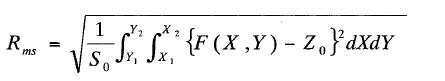
또한, 측정면이란 전체 측정 데이터가 나타내는 면이며, 하기의 식으로 표현한다.
![]()
또한, 지정면이란 거칠기 계측의 대상이 되는 면으로, 좌표 (X1,Y1)(X1,Y2)(X2,Y1)(X2,Y2)로 표시되는 4점에 의해 둘러싸이는 직사각형 영역으로 하고, 지정면이 이상적으로 평탄하다고 했을 때의 면적을 S0라 한다. 또한, S0는 하기의 식으로 구할 수 있다.
![]()
또한, 기준면이란 지정면의 평균 높이에서의, XY 평면과 평행한 면을 말한다. 즉, 지정면의 높이 평균값을 Z0라 할 때, 기준면의 높이도 Z0으로 표현된다. 또한, Z0은 하기의 식으로 구할 수 있다.
![]()
또한, 도 1의 트랜지스터(162)에서는 미세화에 기인하여 소자 사이에 발생하는 누설을 억제하기 위해, 섬형상으로 가공된 산화물 반도체층(144)을 사용하고 있는데, 섬형상으로 가공되지 않은 구성을 채용하여도 좋다. 산화물 반도체층을 섬형상으로 가공하지 않는 경우에는 가공시의 에칭으로 인한 산화물 반도체층(144)의 오염을 방지할 수 있다.
또한, 트랜지스터(162)에 있어서, 소스 전극 또는 드레인 전극(142a), 및 소스 전극 또는 드레인 전극(142b)의 단부는 테이퍼 형상인 것이 바람직하다. 소스 전극 또는 드레인 전극(142a), 소스 전극 또는 드레인 전극(142b)의 단부를 테이퍼 형상으로 함으로써, 산화물 반도체층(144)의 피복성이 향상되며 단 끊어짐을 방지할 수 있기 때문이다. 여기서, 테이퍼 각도는 예를 들면 30°이상 60°이하로 한다. 또한, 테이퍼 각도란, 테이퍼 형상을 갖는 층(예를 들면, 소스 전극 또는 드레인 전극(142a))을 그 단면(기판의 표면과 직교하는 면)에 수직인 방향에서 관찰했을 때에, 해당층의 측면과 저면이 이루는 경사각을 나타낸다.
트랜지스터(162) 위에는 절연층(150)이 형성되어 있으며, 절연층(150) 위에는 절연층(152)이 형성되어 있다. 그리고, 절연층(152) 위에는 트랜지스터(160) 또는 트랜지스터(162)와 접속하는 배선(156)이 형성된다.
<반도체 장치의 제작방법>
이어, 상기 반도체 장치의 제작방법의 일 예에 대해 설명한다. 이하에서는 먼저 하부 트랜지스터(160)의 제작방법에 대해 도 2 및 도 3을 참조하여 설명하고, 그 후, 상부 트랜지스터(162)의 제작방법에 대해 도 4 및 도 5를 참조하여 설명한다.
<하부 트랜지스터의 제작방법>
먼저, 반도체 재료를 포함하는 기판(100)을 준비한다(도 2(A) 참조). 반도체 재료를 포함하는 기판(100)으로서는 실리콘이나 탄화실리콘 등의 단결정 반도체기판, 다결정 반도체 기판, 실리콘 게르마늄 등의 화합물 반도체 기판, SOI 기판 등을 적용할 수 있다. 여기에서는 반도체 재료를 포함하는 기판(100)으로서, 단결정 실리콘 기판을 사용하는 경우의 일 예에 대해 나타낸 것으로 한다. 또한, 일반적으로 'SOI 기판'은 절연 표면 위에 실리콘 반도체층이 형성된 구성의 기판을 말하는데, 본 명세서 등에서는 절연 표면 위에 실리콘 이외의 재료로 이루어진 반도체층이 형성된 구성의 기판도 포함하는 것으로 한다. 즉, 'SOI 기판'이 갖는 반도체층은 실리콘 반도체층으로 한정되지 않는다. 또한, SOI 기판에는 유리 기판 등의 절연기판 위에 절연층을 통해 반도체층이 형성된 구성의 것이 포함되는 것으로 한다.
반도체 재료를 포함하는 기판(100)으로서, 특히 실리콘 등의 단결정 반도체 기판을 사용하는 경우에는 트랜지스터(160)의 동작을 고속화할 수 있기 때문에 바람직하다.
기판(100) 위에는 소자분리절연층을 형성하기 위한 마스크가 되는 보호층(102)을 형성한다(도 2(A) 참조). 보호층(102)으로서는 예를 들면 산화실리콘, 질화실리콘, 산화질화실리콘 또는 질화산화실리콘 등을 재료로 하는 절연층을 사용할 수 있다. 또한, 이 공정의 전후에, 트랜지스터의 문턱 전압을 제어하기 위해, n형의 도전성을 부여하는 불순물 원소나 p형 도전성을 부여하는 불순물 원소를 기판(100)에 첨가하여도 좋다. 반도체가 실리콘인 경우, n형의 도전성을 부여하는 불순물로서는 예를 들면 인이나 비소 등을 사용할 수 있다. 또한, p형 도전성을 부여하는 불순물로서는 예를 들면 비소, 알루미늄, 갈륨 등을 사용할 수 있다.
이어, 상기의 보호층(102)을 마스크로 하여 에칭을 하여, 보호층(102)으로 덮여있지 않은 영역(노출되어 있는 영역)의 기판(100) 일부를 제거한다. 이로써, 다른 반도체영역과 분리된 반도체영역(104)이 형성된다(도 2(B) 참조). 해당 에칭에는 건식 에칭을 사용하는 것이 바람직하지만, 습식 에칭을 사용하여도 좋다. 에칭가스나 에칭액에 대해서는 피에칭재료에 따라 적절히 선택할 수 있다.
그 후, 반도체영역(104)을 덮도록 절연층을 형성하고, 반도체영역(104)에 중첩하는 영역의 절연층을 선택적으로 제거함으로써, 소자분리절연층(106)을 형성한다(도 2(C) 참조). 해당 절연층은 산화실리콘, 질화실리콘, 산화질화실리콘 또는 질화산화실리콘 등을 사용하여 형성된다. 절연층의 제거방법으로서는 화학적 기계적 연마(Chemical Mechanical Polishing : CMP) 처리 등의 연마 처리나 에칭 처리 등이 있는데, 그 중 어느 것을 사용하여도 좋으며, 그들을 조합하여 사용하여도 좋다. 또한, 반도체영역(104)의 형성 후, 또는 소자분리절연층(106)의 형성 후에는 상기 보호층(102)을 제거한다.
또한, 소자분리절연층(106)의 형성방법으로서, 절연층을 선택적으로 제거하는 방법 외에, 산소를 주입함으로써 절연성의 영역을 형성하는 방법 등을 사용할 수도 있다.
이어, 반도체영역(104)의 표면에 절연층을 형성하고, 해당 절연층 위에 도전재료를 포함하는 층을 형성한다.
절연층은 이후 게이트 절연층이 되는 것으로, 예를 들면, 반도체영역(104) 표면의 열처리(열산화처리나 열질화처리 등)에 의해 형성할 수 있다. 열처리 대신에, 고밀도 플라즈마 처리를 적용하여도 좋다. 고밀도 플라즈마 처리는 예를 들면 He, Ar, Kr, Xe 등의 희가스, 산소, 산화질소, 암모니아, 질소, 수소 등 중 어느 한 혼합가스를 사용하여 수행할 수 있다. 물론, CVD법이나 스퍼터링법 등을 사용하여 절연층을 형성하여도 좋다. 해당 절연층은 산화실리콘, 산화질화실리콘, 질화산화실리콘, 질화실리콘, 산화하프늄, 산화알루미늄, 산화탄탈, 산화이트륨, 하프늄 실리게이트(HfSixOy(x>0, y>0)), 질소가 첨가된 하프늄 실리게이트(HfSixOy(x>0, y>0)), 질소가 첨가된 하프늄 알루미네이트(HfAlxOy(x>0, y>0)) 등을 포함하는 단층 구조 또는 적층 구조로 하는 것이 바람직하다. 또한, 절연층의 두께는 1nm 이상 100nm 이하, 바람직하게는 10nm 이상 50nm 이하로 할 수 있다.
도전재료를 포함하는 층은 알루미늄이나 구리, 티탄, 탄탈, 텅스텐 등의 금속재료를 사용하여 형성할 수 있다. 또한, 다결정 실리콘 등의 반도체 재료를 사용하여, 도전재료를 포함하는 층을 형성하여도 좋다. 형성방법도 특별히 한정되지 않으며, 증착법, CVD법, 스퍼터링법, 스핀 코팅법 등의 각종 성막방법을 사용할 수 있다. 또한, 본 실시형태에서는 도전재료를 포함하는 층을 금속재료를 사용하여 형성하는 경우의 일 예에 대해 나타낸 것으로 한다.
그 후, 절연층 및 도전재료를 포함하는 층을 선택적으로 에칭하여 게이트 절연층(108), 게이트 전극(110)을 형성한다(도 2(C) 참조).
이어, 반도체영역(104)에 인(P)이나 비소(As) 등을 첨가하여 채널형성영역(116) 및 불순물영역(120)을 형성한다(도 2(D) 참조). 또한, 여기에서는 n형 트랜지스터를 형성하기 위해 인이나 비소를 첨가하고 있는데, p형 트랜지스터를 형성하는 경우에는 붕소(B)나 알루미늄(Al) 등의 불순물 원소를 첨가하면 된다. 여기서, 첨가하는 불순물의 농도는 적절히 설정할 수 있지만, 반도체 소자가 고도로 미세화되는 경우에는 그 농도를 높게 하는 것이 바람직하다.
또한, 게이트 전극(110)의 주위에 측벽 절연층을 형성하여, 불순물 원소가 다른 농도로 첨가된 불순물영역을 형성하여도 좋다.
이어, 게이트 전극(110), 불순물영역(120) 등을 덮도록 금속층(122)을 형성한다(도 3(A) 참조). 해당 금속층(122)은 진공증착법이나 스퍼터링법, 스핀 코팅법 등의 각종 성막방법으로 형성할 수 있다. 금속층(122)은 반도체영역(104)을 구성하는 반도체 재료와 반응함으로써 저저항의 금속 화합물이 되는 금속재료를 사용하여 형성하는 것이 바람직하다. 이와 같은 금속재료로서는 예를 들면, 티탄, 탄탈, 텅스텐, 니켈, 코발트, 백금 등이 있다.
그 후, 열처리를 실시하여 상기 금속층(122)과 반도체 재료를 반응시킨다. 이로써, 불순물영역(120)에 접하는 금속화합물영역(124)이 형성된다(도 3(A) 참조). 또한, 게이트 전극(110)으로서 다결정 실리콘 등을 사용할 경우에는 게이트 전극(110)의 금속층(122)과 접촉하는 부분에도 금속화합물영역이 형성되게 된다.
상기 열처리로서는 예를 들면 플래시 램프의 조사에 의한 열처리를 사용할 수 있다. 물론, 기타의 열처리방법을 사용하여도 좋지만, 금속 화합물의 형성과 관련된 화학반응의 제어성을 향상시키기 위해서는 극히 단시간의 열처리를 실현할 수 있는 방법을 사용하는 것이 바람직하다. 또한, 상기의 금속화합물 영역은 금속재료와 반도체 재료의 반응에 의해 형성되는 것이며, 충분히 도전성이 높아진 영역이다. 해당 금속화합물영역을 형성함으로써, 전기 저항을 충분히 저감하고 소자 특성을 향상시킬 수 있다. 또한, 금속화합물영역(124)을 형성한 후에는 금속층(122)은 제거한다.
이어, 상술한 공정에 의해 형성된 각 구성을 덮도록 절연층(128), 절연층(130)을 형성한다(도 3(B) 참조). 절연층(128)이나 절연층(130)은 산화실리콘, 산화질화실리콘, 산화알루미늄 등의 무기절연재료를 포함하는 재료를 사용하여 형성할 수 있다. 특히, 절연층(128)이나 절연층(130)에 유전율이 낮은(low-k) 재료를 사용함으로써, 각종 전극이나 배선의 오버랩에 기인하는 용량을 충분히 저감하는 것이 가능해지기 때문에 바람직하다. 또한, 절연층(128)이나 절연층(130)에는 이들 재료를 사용한 다공성 절연층을 적용하여도 좋다. 다공성 절연층에서는 밀도가 높은 절연층에 비해 유전율이 저하되기 때문에, 전극이나 배선에 기인하는 용량을 더욱 저감하는 것이 가능하다.
또한, 절연층(128)이나 절연층(130) 중에, 질화산화실리콘, 질화실리콘 등의 질소를 많이 포함하는 무기절연재료로 이루어진 층을 포함하여도 좋다. 이로써, 하부 트랜지스터(160)를 구성하는 재료가 포함하는 물이나 수소 등의 불순물이 이후에 형성하는 상부 트랜지스터(162)의 산화물 반도체층(144)에 침입하는 것을 방지할 수 있다. 단, 이 경우, 이후의 공정에서 수행하는 CMP처리만으로는 질소를 많이 포함하는 무기절연재료로 이루어진 층의 제거가 곤란하므로, 에칭 처리 등을 병용하는 것이 바람직하다.
예를 들면, 절연층(128)으로서 산화질화실리콘을 형성하고, 절연층(130)으로서 산화실리콘을 형성할 수 있다. 이와 같이, 절연층(128) 및 절연층(130)을 산화질화실리콘이나 산화실리콘과 같은 산소를 많이 포함하는 무기절연재료만을 사용하여 형성함으로써, 이후의 공정에서 절연층(128) 및 절연층(130)에 용이하게 CMP처리를 실시할 수 있다.
또한, 여기에서는 절연층(128)과 절연층(130)의 적층 구조로 하고 있지만, 개시하는 발명의 일 양태는 이에 한정되지 않는다. 1층으로 하여도 좋고, 3층 이상의 적층 구조로 하여도 좋다. 예를 들면, 상기 절연층(128)으로서 산화질화실리콘을 형성하고 절연층(130)으로서 산화실리콘을 형성하는 구성에 있어, 추가로 절연층(128)과 절연층(130) 사이에 질화산화실리콘막을 형성하는 구성으로 하여도 좋다.
또한, 본 명세서 중에 있어서, '산화질화실리콘'이란 그 조성으로서 질소보다도 산소의 함유량이 많은 것을 가리키며, '질화산화실리콘'이란 그 조성으로서 산소보다도 질소의 함유량이 많은 것을 가리킨다.
이상에 따라, 반도체 재료를 포함하는 기판(100)을 사용한 트랜지스터(160)가 형성된다(도 3(B) 참조). 이와 같은 트랜지스터(160)는 고속 동작이 가능하다는 특징을 갖는다.
그 후, 트랜지스터(162) 형성 전의 처리로서, 절연층(128)이나 절연층(130)에 화학적 기계적 연마(Chemical Mechanical Polishing : CMP) 처리를 실시하여 절연층(128) 및 절연층(130)의 표면을 평탄화한다(도 3(C) 참조). 여기에서, CMP처리란 피가공물의 표면을 기준으로 하며, 이에 따라 표면을 화학적/기계적인 복합작용에 의해 평탄화하는 수법이다. 일반적으로 연마 스테이지 위에 연마포를 부착하고, 피가공물과 연마포 사이에 슬러리(연마제)를 공급하면서 연마 스테이지와 피가공물을 각각 회전 또는 요동시켜 피가공물의 표면을, 슬러리와 피가공물 표면 사이에서의 화학반응 및 연마포와 피가공물의 기계적 연마 작용에 의해 피가공물의 표면을 연마하는 방법이다.
CMP처리는 1회 실시하여도 좋고, 복수회 실시하여도 좋다. 복수회로 나눠 CMP처리를 실시할 경우에는 높은 연마율의 1차 연마를 수행한 후, 낮은 연마율의 마무리 연마를 수행하는 것이 바람직하다. 이와 같이 연마율이 다른 연마를 조합함으로써, 절연층(128) 및 절연층(130) 표면의 평탄성을 더욱 향상시킬 수 있다.
절연층(128) 및 절연층(130)을 평탄화시키는 처리로서는 CMP처리 외에 에칭 처리 등을 적용하는 것도 가능하지만, 산화물 반도체층(144)의 평탄성 및 균일성을 향상시키고 트랜지스터(162)의 특성을 향상시키기 위해, 절연층(128)이나 절연층(130)의 표면은 RMS 거칠기가 1nm 이하, 바람직하게는 0.5nm 이하가 되도록 평탄화해 두는 것이 바람직하다.
또한, 절연층(128) 및 절연층(130)의 적층 구조에, 질화실리콘이나 질화산화실리콘과 같은 질소를 많이 포함하는 무기절연재료가 포함될 경우, CMP처리만으로는 질소를 많이 포함하는 무기절연재료의 제거가 곤란하므로, 에칭 처리 등을 병용하는 것이 바람직하다. 질소를 많이 포함하는 무기절연재료의 에칭 처리에는 건식 에칭, 습식 에칭 중 어느 것을 사용하여도 좋지만, 소자의 미세화라는 관점에서는 건식 에칭을 사용하는 것이 바람직하다. 또한, 각 절연층의 에칭률이 균일해지도록 에칭 조건(에칭가스나 에칭액, 에칭시간, 온도 등)을 적절히 설정하는 것이 바람직하다. 또한, 건식 에칭에 사용하는 에칭가스에는 예를 들면, 불소를 포함하는 가스(트리플루오로메탄(CHF3))나, 추가로 헬륨(He)이나 아르곤(Ar) 등의 희가스를 첨가한 가스 등을 사용할 수 있다.
또한, 상기의 각 공정의 전후에는 추가로 전극이나 배선, 반도체층, 절연층 등을 형성하는 공정을 포함하고 있어도 좋다. 예를 들면, 배선 구조로서, 절연층 및 도전층의 적층 구조로 이루어진 다층 배선구조를 채용하여, 고도로 집적화된 반도체 장치를 실현하는 것도 가능하다.
<상부 트랜지스터의 제작방법>
이어, 게이트 전극(110), 절연층(128), 절연층(130) 등의 위에 도전층을 형성하고, 이 도전층을 선택적으로 에칭하여 소스 전극 또는 드레인 전극(142a), 소스 전극 또는 드레인 전극(142b)을 형성한다(도 4(A) 참조).
도전층은 스퍼터링법을 비롯한 PVD법이나, 플라즈마 CVD법 등의 CVD법을 사용하여 형성할 수 있다. 또한, 도전층의 재료로서는 알루미늄, 크롬, 구리, 탄탈, 티탄, 몰리브덴, 텅스텐 중에서 선택된 원소나, 상술한 원소를 성분으로 하는 합금 등을 사용할 수 있다. 망간, 마그네슘, 지르코늄, 베릴륨, 네오디뮴, 스칸듐 중 어느 하나 또는 이들을 복수 조합한 재료를 사용하여도 좋다.
도전층은 단층 구조이어도 좋고, 2층 이상의 적층 구조로 하여도 좋다. 예를 들면, 티탄막이나 질화티탄막의 단층 구조, 실리콘을 포함하는 알루미늄막의 단층 구조, 알루미늄막 위에 티탄막이 적층된 2층 구조, 질화티탄막 위에 티탄막이 적층된 2층 구조, 티탄막과 알루미늄막과 티탄막이 적층된 3층 구조 등을 들 수 있다. 또한, 도전층을 티탄막이나 질화티탄막의 단층 구조로 하는 경우에는 테이퍼 형상을 갖는 소스 전극 또는 드레인 전극(142a), 및 소스 전극 또는 드레인 전극(142b)으로의 가공이 용이하다는 이점이 있다.
또한, 도전층은 도전성 금속 산화물을 사용하여 형성하여도 좋다. 도전성 금속산화물로서는 산화인듐(In2O3), 산화주석(SnO2), 산화아연(ZnO), 산화인듐 산화주석 합금(In2O3-SnO2, ITO라 약칭하는 경우가 있다), 산화인듐 산화아연 합금(In2O3-ZnO), 또는 이들 금속 산화물 재료에 실리콘 또는 산화실리콘을 함유시킨 것을 사용할 수 있다.
도전층의 에칭은 형성되는 소스 전극 또는 드레인 전극(142a), 및 소스 전극 또는 드레인 전극(142b)의 단부가 테이퍼 형상이 되도록 수행하는 것이 바람직하다. 여기서, 테이퍼 각도은 예를 들면 30°이상 60°이하인 것이 바람직하다. 소스 전극 또는 드레인 전극(142a), 소스 전극 또는 드레인 전극(142b)의 단부를 테이퍼 형상이 되도록 에칭함으로써, 나중에 형성되는 게이트 절연층(146)의 피복성을 향상시키고 단 끊어짐을 방지할 수 있다.
상부 트랜지스터의 채널 길이(L)는 소스 전극 또는 드레인 전극(142a), 및 소스 전극 또는 드레인 전극(142b)의 하단부의 간격에 의해 결정된다. 또한, 채널 길이(L)가 25nm 미만인 트랜지스터를 형성하는 경우에 사용하는 마스크 형성의 노광을 수행할 때에는 수 nm~수 10nm과 파장이 짧은 초자외선(Extreme Ultraviolet)을 사용하는 것이 바람직하다. 초자외선에 의한 노광은 해상도가 높고 초점심도도 크다. 따라서, 나중에 형성되는 트랜지스터의 채널길이(L)를 10nm 이상 1000nm(1μm) 이하로 하는 것도 가능하며, 회로의 동작속도를 높이는 것이 가능하다. 또한, 미세화에 의해 반도체 장치의 소비 전력을 저감하는 것도 가능하다.
또한, 절연층(128)이나 절연층(130) 위에는 베이스로서 기능하는 절연층을 형성하여도 좋다. 해당 절연층은 PVD법이나 CVD법 등을 사용하여 형성할 수 있다. 이 경우, 형성한 절연층도 RMS 거칠기가 1nm 이하, 바람직하게는 0.5nm 이하인 표면을 갖는 것이 바람직하다.
이어, 소스 전극 또는 드레인 전극(142a) 위에 절연층(143a)을, 소스 전극 또는 드레인 전극(142b) 위에 절연층(143b)을 각각 형성한다(도 4(B) 참조). 절연층(143a) 및 절연층(143b)은 소스 전극 또는 드레인 전극(142a)이나, 소스 전극 또는 드레인 전극(142b)을 덮는 절연층을 형성한 후, 해당 절연층을 선택적으로 에칭함으로써 형성할 수 있다. 또한, 절연층(143a) 및 절연층(143b)은 나중에 형성되는 게이트 전극의 일부와 중첩하도록 형성한다. 이와 같은 절연층을 형성함으로써, 게이트 전극과 소스 전극 또는 드레인 전극과의 사이의 용량을 저감하는 것이 가능하다.
절연층(143a)이나 절연층(143b)은 산화실리콘, 산화질화실리콘, 질화산화실리콘, 질화실리콘, 산화알루미늄 등의 무기절연재료를 포함하는 재료를 사용하여 형성할 수 있다. 특히, 절연층(143a)이나 절연층(143b)에 유전율이 낮은(low-k) 재료를 사용함으로써, 게이트 전극과 소스 전극 또는 드레인 전극과의 사이의 용량을 충분히 저감하는 것이 가능하게 되기 때문에 바람직하다. 또한, 절연층(143a)이나 절연층(143b)에는 이들 재료를 사용한 다공성 절연층을 적용하여도 좋다. 다공성 절연층에서는 밀도가 높은 절연층에 비해 유전율이 저하되기 때문에, 게이트 전극과 소스 전극 또는 드레인 전극과의 사이의 용량을 더욱 저감하는 것이 가능하다.
또한, 게이트 전극과 소스 전극 또는 드레인 전극과의 사이의 용량을 저감시킨다는 점에서는 절연층(143a) 및 절연층(143b)을 형성하는 것이 바람직하지만, 해당 절연층을 형성하지 않는 구성으로 하는 것도 가능하다.
이어, 소스 전극 또는 드레인 전극(142a), 및 소스 전극 또는 드레인 전극(142b)을 덮도록 산화물 반도체층을 형성한 후, 해당 산화물 반도체층을 선택적으로 에칭하여 산화물 반도체층(144)을 형성한다(도 4(C) 참조).
산화물 반도체층은 4원계 금속 산화물인 In-Sn-Ga-Zn-O계나, 3원계 금속 산화물인 In-Ga-Zn-O계, In-Sn-Zn-O계, In-Al-Zn-O계, Sn-Ga-Zn-O계, Al-Ga-Zn-O계, Sn-Al-Zn-O계나, 2원계 금속 산화물인 In-Zn-O계, Sn-Zn-O계, Al-Zn-O계, Zn-Mg-O계, Sn-Mg-O계, In-Mg-O계나, In-O계, Sn-O계, Zn-O계 등을 사용하여 형성할 수 있다.
그 중에서도, In-Ga-Zn-O계의 산화물 반도체 재료는 무전계시의 저항이 충분히 높아 오프 전류를 충분히 작게 하는 것이 가능하며, 또한, 전계효과이동도도 높기 때문에, 반도체 장치에 사용하는 반도체 재료로서는 바람직하다.
In-Ga-Zn-O계 산화물 반도체 재료의 대표예로서는 InGaO3(ZnO)m(m>0)으로 표기되는 것이 있다. 또한, Ga 대신에 M을 사용하고, InMO3(ZnO)m(m>0)과 같이 표기되는 산화물 반도체 재료가 있다. 여기서, M은 갈륨(Ga), 알루미늄(Al), 철(Fe), 니켈(Ni), 망간(Mn), 코발트(Co) 등에서 선택된 하나의 금속원소 또는 복수의 금속원소를 나타낸다. 예를 들면, M으로서는 Ga, Ga 및 Al, Ga 및 Fe, Ga 및 Ni, Ga 및 Mn, Ga 및 Co 등을 적용할 수 있다. 또한, 상술한 조성은 결정구조로부터 도출되는 것으로, 어디까지나 일 예에 지나지 않음을 밝힌다.
산화물 반도체층을 스퍼터링법으로 제작하기 위한 타겟으로서는 In:Ga:Zn=1:x:y(x는 0이상, y는 0.5이상 5이하)의 조성식으로 표시되는 것을 사용하는 것이 바람직하다. 예를 들면, In2O3:Ga2O3:ZnO=1:1:2[mol수 비]의 조성비를 갖는 타겟 등을 사용할 수 있다. 또한, In2O3:Ga2O3:ZnO=1:1:1[mol수 비]의 조성비를 갖는 타겟이나, In2O3:Ga2O3:ZnO=1:1:4[mol수 비]의 조성비를 갖는 타겟이나, In2O3:Ga2O3:ZnO=1:0:2[mol수 비]의 조성비를 갖는 타겟을 사용할 수도 있다.
본 실시형태에서는 산화물 반도체층을 In-Ga-Zn-O계 금속 산화물 타겟을 사용하는 스퍼터링법에 의해 형성하는 것으로 한다.
금속 산화물 타겟 중의 금속 산화물의 상대밀도는 80% 이상, 바람직하게는 95% 이상, 더욱 바람직하게는 99.9% 이상이다. 상대밀도가 높은 금속 산화물 타겟을 사용함으로써, 치밀한 구조의 산화물 반도체층을 형성하는 것이 가능하다.
산화물 반도체층의 형성 분위기는 희가스(대표적으로는 아르곤) 분위기, 산소 분위기, 또는 희가스(대표적으로는 아르곤)와 산소의 혼합 분위기로 하는 것이 바람직하다. 구체적으로는 예를 들면 수소, 물, 수산기, 수소화물 등의 불순물이 농도 1ppm 이하(바람직하게는 농도 10ppb 이하)로까지 제거된 고순도 가스 분위기를 사용하는 것이 바람직하다.
산화물 반도체층의 형성시에는 예를 들면, 감압 상태로 유지된 처리실 내에 피처리물을 홀딩하고, 피처리물의 온도가 100℃ 이상 550℃ 미만, 바람직하게는 200℃ 이상 400℃ 이하가 되도록 피처리물을 가열한다. 혹은, 산화물 반도체층의 형성시 피처리물의 온도는 실온(25℃±10℃)으로 하여도 좋다. 그리고, 처리실 내의 수분을 제거하면서, 수소나 물 등이 제거된 스퍼터링 가스를 도입하고, 상기 타겟을 사용하여 산화물 반도체층을 형성한다. 피처리물을 가열하면서 산화물 반도체층을 형성함으로써, 산화물 반도체층에 포함되는 불순물을 저감할 수 있다. 또한, 스퍼터링에 의한 손상을 경감할 수 있다. 처리실 내의 수분을 제거하기 위해서는 흡착형 진공 펌프를 사용하는 것이 바람직하다. 예를 들면, 크라이오펌프, 이온펌프, 티타늄 서블리메이션 펌프(titanium sublimation pump) 등을 사용할 수 있다. 또한, 터보 펌프에 콜드 트랩을 조합한 것을 사용하여도 좋다. 크라이오 펌프를 사용하여 배기함으로써, 처리실로부터 수소나 물 등을 제거할 수 있기 때문에, 산화물 반도체층 중의 불순물 농도를 저감할 수 있다.
산화물 반도체층의 형성조건으로서는 예를 들면, 피처리물과 타겟간의 거리가 170mm, 압력이 0.4Pa, 직류(DC) 전력이 0.5kW, 분위기가 산소(산소 100%) 분위기, 또는 아르곤(아르곤 100%) 분위기, 또는 산소와 아르곤의 혼합 분위기라는 조건을 적용할 수 있다. 또한, 펄스 직류(DC) 전원을 사용하면, 먼지(성막시에 형성되는 가루형태의 물질 등)를 저감할 수 있으며, 막두께 분포도 균일해지기 때문에 바람직하다. 산화물 반도체층의 두께는 1nm 이상 50nm 이하, 바람직하게는 1nm 이상 30nm 이하, 보다 바람직하게는 1nm 이상 10nm 이하로 한다. 이와 같은 두께의 산화물 반도체층을 사용함으로써, 미세화에 수반되는 쇼트채널효과를 억제하는 것이 가능하다. 단, 적용하는 산화물 반도체 재료나 반도체 장치의 용도 등에 따라 적절한 두께는 다르기 때문에, 그 두께는 사용하는 재료나 용도 등에 따라 선택할 수도 있다.
여기서, 산화물 반도체층(144)은 RMS 거칠기가 1nm 이하, 바람직하게는 0.5nm 이하인 표면을 갖는 절연층(130) 위에 형성된다. 이와 같이, 평탄성이 양호한 표면 위에 산화물 반도체층(144)을 형성함으로써, 산화물 반도체층(144)의 평탄성 및 균일성을 양호한 것으로 할 수 있다. 추가로, 평탄성 및 균일성이 양호한 산화물 반도체층(144)을 사용함으로써, 트랜지스터(162)의 트랜지스터 특성을 향상시킬 수 있다.
또한, 산화물 반도체층을 스퍼터링법에 의해 형성하기 전에는 아르곤 가스를 도입하여 플라즈마를 발생시키는 역스퍼터링을 수행하여, 형성 표면(예를 들면 절연층(130)의 표면)의 부착물을 제거하는 것이 바람직하다. 여기서, 역스퍼터링이란 통상의 스퍼터링에서는 스퍼터링 타겟에 이온을 충돌시키는 바를, 역으로 기판의 처리 표면에 이온을 충돌시킴으로써 그 표면을 개질하는 방법을 말한다. 처리 표면에 이온을 충돌시키는 방법으로서는 아르곤 분위기하에서 처리 표면측에 고주파 전압을 인가하여 피처리물 부근에 플라즈마를 생성하는 방법 등이 있다. 또한, 아르곤 분위기를 대신하여 질소, 헬륨, 산소 등의 분위기를 적용하여도 좋다.
그 후, 산화물 반도체층에 대해, 열처리(제 1 열처리)를 실시하는 것이 바람직하다. 이 제 1 열처리에 의해 산화물 반도체층 중의 과잉 수소(물이나 수산기를 포함함)를 제거하고 산화물 반도체층의 구조를 조정하여, 에너지 갭 중의 결함 준위를 저감할 수 있다. 제 1 열처리의 온도는 예를 들면 300℃ 이상 550℃ 미만, 또는 400℃ 이상 500℃ 이하로 한다.
열처리는 예를 들면 저항 발열체 등을 사용한 전기로에 피처리물을 도입하고, 질소 분위기 하, 450℃, 1시간의 조건에서 수행할 수 있다. 그동안, 산화물 반도체층은 물이나 수소의 혼입이 발생하지 않도록 대기에 노출시키지 않는다.
열처리장치는 전기로에 한정되지 않고, 가열된 가스 등의 매체로부터의 열전도 또는 열복사에 의해 피처리물을 가열하는 장치를 사용하여도 좋다. 예를 들면, GRTA(Gas Rapid Thermal Anneal) 장치, LRTA(Lamp Rapid Thermal Anneal) 장치 등의 RTA(Rapid Thermal Anneal) 장치를 사용할 수 있다. LRTA 장치는 할로겐 램프, 메탈 할라이드 램프, 크세논 아크 램프, 카본 아크 램프, 고압 나트륨 램프, 고압 수은 램프 등의 램프에서 발하는 광(전자파)의 복사에 의해 피처리물을 가열하는 장치이다. GRTA 장치는 고온의 가스를 사용하여 열처리를 수행하는 장치이다. 가스로서는 아르곤 등의 희가스, 또는 질소와 같은 열처리에 의해 피처리물과 반응하지 않는 비활성 기체가 사용된다.
예를 들면, 제 1 열처리로서, 가열된 비활성 가스 분위기 중에 피처리물을 투입하고, 수분 동안 가열한 후, 해당 비활성 가스 분위기로부터 피처리물을 꺼내는 GRTA 처리를 실시하여도 좋다. GRTA 처리를 사용하면 단시간으로 고온 열처리가 가능하게 된다. 또한, 피처리물의 내열 온도를 초과하는 온도 조건이더라도 적용이 가능하게 된다. 또한, 처리 중에, 비활성 가스를, 산소를 포함하는 가스로 전환하여도 좋다. 산소를 포함하는 분위기에서 제 1 열처리를 실시함으로써, 산소 결손에 기인하는 에너지 갭 중의 결함 준위를 저감할 수 있기 때문이다.
또한, 비활성 가스 분위기로서는 질소, 또는 희가스(헬륨, 네온, 아르곤 등)를 주성분으로 하는 분위기이면서 물, 수소 등이 포함되지 않는 분위기를 적용하는 것이 바람직하다. 예를 들면, 열처리 장치에 도입하는 질소나 헬륨, 네온, 아르곤 등의 희가스의 순도를 6N(99.9999%) 이상, 바람직하게는 7N(99.99999%) 이상(즉, 불순물 농도가 1ppm 이하, 바람직하게는 0.1ppm 이하)으로 한다.
어느 것으로 하든, 제 1 열처리에 의해 불순물을 저감하고 i형(진성 반도체) 또는 i형에 매우 가까운 산화물 반도체층을 형성함으로써, 매우 우수한 특성의 트랜지스터를 실현할 수 있다.
그런데, 상술한 열처리(제 1 열처리)에는 수소나 물 등을 제거하는 효과가 있으므로, 해당 열처리를 탈수화처리나 탈수소화처리 등으로 부를 수도 있다. 해당 탈수화처리나 탈수소화처리는 산화물 반도체층의 형성 후나 게이트 절연층의 형성 후, 게이트 전극의 형성 후 등의 타이밍에서 수행하는 것도 가능하다. 또한, 이와 같은 탈수화처리, 탈수소화처리는 1회에 국한되지 않고 복수회 실시하여도 좋다.
산화물 반도체층의 에칭은 상기 열처리 전, 또는 상기 열처리 후 중 어느 쪽에서든 실시하여도 좋다. 또한, 소자의 미세화라는 관점에서는 건식 에칭을 사용하는 것이 바람직하지만, 습식 에칭을 사용하여도 좋다. 에칭가스나 에칭액에 대해서는 피에칭재료에 따라 적절히 선택할 수 있다. 또한, 소자에서의 누설 등이 문제가 되지 않을 경우에는 산화물 반도체층을 섬형상으로 가공하지 않고 사용하여도 좋다.
이어, 산화물 반도체층(144)에 접하는 게이트 절연층(146)을 형성하고, 그 후, 게이트 절연층(146) 위에서 산화물 반도체층(144)과 중첩하는 영역에 게이트 전극(148a)을 형성한다(도 5(A) 참조).
게이트 절연층(146)은 CVD법이나 스퍼터링법 등을 사용하여 형성할 수 있다. 또한, 게이트 절연층(146)은 산화실리콘, 질화실리콘, 산화질화실리콘, 질화산화실리콘, 산화알루미늄, 산화탄탈, 산화하프늄, 산화이트륨, 하프늄 실리케이트(HfSixOy(x>0, y>0)), 질소가 첨가된 하프늄 실리게이트(HfSixOy(x>0, y>0)), 질소가 첨가된 하프늄 알루미네이트(HfAlxOy(x>0, y>0)) 등을 포함하도록 형성하는 것이 바람직하다. 게이트 절연층(146)은 단층 구조로 하여도 좋고 적층 구조로 하여도 좋다. 또한, 그 두께는 특별히 한정되지 않지만, 반도체 장치를 미세화할 경우에는 트랜지스터의 동작을 확보하기 위해 얇게 하는 것이 바람직하다. 예를 들면, 산화실리콘을 사용하는 경우에는 1nm 이상 100nm 이하, 바람직하게는 10nm 이상 50nm 이하로 할 수 있다.
상술한 바와 같이, 게이트 절연층을 얇게 하면, 터널효과 등에 기인하는 게이트 누설이 문제가 된다. 게이트 누설의 문제를 해소하기 위해서는 게이트 절연층(146)에 산화하프늄, 산화탄탈, 산화이트륨, 하프늄 실리케이트(HfSixOy(x>0, y>0)), 질소가 첨가된 하프늄 실리게이트(HfSixOy(x>0, y>0)), 질소가 첨가된 하프늄 알루미네이트(HfAlxOy(x>0, y>0)) 등의 고유전율(high-k) 재료를 사용하면 된다. high-k 재료를 게이트 절연층(146)에 사용함으로써, 전기적 특성을 확보하면서 게이트 누설을 억제하기 위해 막두께를 크게 하는 것이 가능하게 된다. 또한, high-k 재료를 포함하는 막과, 산화실리콘, 질화실리콘, 산화질화실리콘, 질화산화실리콘, 산화알루미늄 등 중 어느 하나를 포함하는 막과의 적층구조로 하여도 좋다.
게이트 절연층(146)의 형성 후에는 비활성 가스 분위기, 또는 산소 분위기 하에서 제 2 열처리를 실시하는 것이 바람직하다. 열처리의 온도는 200℃ 이상 450℃ 이하, 바람직하게는 250℃ 이상 350℃ 이하이다. 예를 들면, 질소 분위기하에 250℃에서 1시간 동안 열처리를 실시하면 된다. 제 2 열처리를 실시함으로써, 트랜지스터의 전기적 특성의 편차를 경감할 수 있다. 또한, 게이트 절연층(146)이 산소를 포함하는 경우, 산화물 반도체층(144)에 산소를 공급하고 이 산화물 반도체층(144)의 산소 결손을 보충하여, i형(진성 반도체) 또는 i형에 매우 가까운 산화물 반도체층을 형성할 수도 있다.
또한, 본 실시형태에서는 게이트 절연층(146)의 형성 후에 제 2 열처리를 실시하고 있는데, 제 2 열처리의 타이밍은 이에 한정되지 않는다. 예를 들면, 게이트 전극의 형성 후에 제 2 열처리를 실시하여도 좋다. 또한, 제 1 열처리에 이어 제 2 열처리를 실시하여도 좋고, 제 1 열처리에 제 2 열처리를 겸하게 하여도 좋으며, 제 2 열처리에 제 1 열처리를 겸하게 하여도 좋다.
상술한 바와 같이, 제 1 열처리와 제 2 열처리 중 적어도 한쪽을 적용함으로써, 산화물 반도체층(144)을 그 주성분 이외의 불순물이 가능한 포함되지 않도록 고순도화할 수 있다.
게이트 전극(148a)은 게이트 절연층(146) 위에 도전층을 형성한 후에, 해당 도전층을 선택적으로 에칭함으로써 형성할 수 있다. 게이트 전극(148a)이 되는 도전층은 스퍼터링법을 비롯한 PVD법이나, 플라즈마 CVD법 등의 CVD법을 사용하여 형성할 수 있다. 상세 사항은 소스 전극 또는 드레인 전극(142a) 등인 경우와 마찬가지이며, 이들 기재를 참작할 수 있다.
이어, 게이트 절연층(146), 게이트 전극(148a) 위에 절연층(150) 및 절연층(152)을 형성한다(도 5(B) 참조). 절연층(150) 및 절연층(152)은 PVD법이나 CVD법 등을 사용하여 형성할 수 있다. 또한, 산화실리콘, 산화질화실리콘, 질화산화실리콘, 질화실리콘, 산화하프늄, 산화알루미늄 등의 무기절연재료를 포함하는 재료를 사용하여 형성할 수 있다.
또한, 절연층(150)이나 절연층(152)에는 유전율이 낮은 재료나, 유전율이 낮은 구조(다공성 구조 등)를 사용하는 것이 바람직하다. 절연층(150)이나 절연층(152)의 유전율을 낮게 함으로써, 배선이나 전극 등의 사이에 발생하는 용량을 저감하여 동작의 고속화를 도모할 수 있기 때문이다.
또한, 본 실시형태에서는 절연층(150)과 절연층(152)의 적층 구조로 하고 있는데, 개시하는 발명의 일 양태는 이에 한정되지 않는다. 1층으로 하여도 좋으며, 3층 이상의 적층 구조로 하여도 좋다. 또한, 절연층을 형성하지 않는 구성으로 하는 것도 가능하다.
또한, 상기 절연층(152)은 그 표면이 평탄하게 되도록 형성하는 것이 바람직하다. 표면이 평탄해지도록 절연층(152)을 형성함으로써, 반도체 장치를 미세화한 경우 등에서도, 절연층(152) 위에 전극이나 배선 등을 적절하게 형성할 수 있기 때문이다. 또한, 절연층(152)의 평탄화는 CMP 등의 방법을 사용하여 수행할 수 있다.
그리고, 트랜지스터(160) 또는 트랜지스터(162)와 배선(156)을 전기적으로 접속하기 위한 전극(미도시)을 형성한 후, 절연층(152) 위에 배선(156)을 형성한다(도 5(C) 참조). 물론, 이들 요소가 모두 전기적으로 접속될 필요는 없다. 다른 요소로부터 독립된 요소를 갖고 있어도 좋다.
배선(156)은 스퍼터링을 비롯한 PVD법이나, 플라즈마 CVD법 등의 CVD법을 사용하여 도전층을 형성한 후, 해당 도전층을 패터닝함으로써 형성된다. 또한, 도전층 재료로서는 알루미늄, 크롬, 구리, 탄탈, 티탄, 몰리브덴, 텅스텐 중에서 선택된 원소나, 상술한 원소를 성분으로 하는 합금 등을 사용할 수 있다. 망간, 마그네슘, 지르코늄, 베릴륨, 네오디뮴, 스칸듐 중 어느 하나, 또는 이들을 복수 조합한 재료를 사용하여도 좋다. 상세 사항은 소스 전극 또는 드레인 전극(142a) 등과 마찬가지이다.
이상에 따라, 고순도화된 산화물 반도체층(144)을 사용한 트랜지스터(162)가 완성된다(도 5(C) 참조).
이와 같이 고순도화되며 진성화된 산화물 반도체층(144)을 사용함으로써, 트랜지스터(162)의 오프 전류를 충분히 저감할 수 있다.
이상에 따라, 하부에 산화물 반도체 이외의 반도체 재료를 사용한 트랜지스터를 가지며, 상부에 산화물 반도체를 사용한 트랜지스터를 갖는 반도체 장치를 제공할 수 있다.
이와 같이, 산화물 반도체 이외의 반도체 재료를 사용한 트랜지스터와, 산화물 반도체를 사용한 트랜지스터를 일체로 구비하는 구성으로 함으로써, 각각의 특성의 이점을 살린 새로운 반도체 장치를 실현할 수 있다.
또한, 평탄성이 양호한 표면 위에 산화물 반도체층을 형성함으로써 트랜지스터 특성을 향상시킨 트랜지스터를, 산화물 반도체 이외의 반도체 재료를 사용한 트랜지스터에 적층한 반도체 장치를 제공할 수 있다.
이상, 본 실시형태에 나타낸 구성, 방법 등은 다른 실시형태에 나타낸 구성, 방법 등과 적절히 조합하여 사용할 수 있다.
(실시형태 2)
본 실시형태에서는 개시하는 발명의 다른 일 양태에 따른 반도체 장치의 구성 및 그 제작방법에 대해, 도 6~도 13을 참조하여 설명한다. 또한, 본 실시형태에서는 특별히 기억장치로서 사용할 수 있는 반도체 장치의 구성예에 대해 설명한다.
<반도체 장치의 단면 구성 및 평면 구성>
도 6은 반도체 장치의 구성의 일 예이다. 도 6(A)에서는 반도체 장치의 단면을, 도 6(B)에는 반도체 장치의 평면을 각각 나타낸다. 여기서, 도 6(A)는 도 6(B)의 A1-A2 및 B1-B2에 따른 단면에 상당한다. 도 6(A) 및 도 6(B)에 나타나는 반도체 장치는 하부에 제 1 반도체 재료를 사용한 트랜지스터(260)를 가지며, 상부에 제 2 반도체 재료를 사용한 트랜지스터(262)를 갖는 것으로, 트랜지스터(260)의 게이트 전극(210)과, 트랜지스터(262)의 소스 전극 또는 드레인 전극(242a)은 서로 직접 접속되어 있다. 여기서, 제 1 반도체 재료와 제 2 반도체 재료는 서로 다른 재료로 하는 것이 바람직하다. 예를 들면, 제 1 반도체 재료를 산화물 반도체 이외의 반도체 재료로 하고, 제 2 반도체 재료를 산화물 반도체로 할 수 있다. 산화물 반도체 이외의 반도체 재료로서는 예를 들면 실리콘, 게르마늄, 실리콘 게르마늄, 탄화실리콘, 또는 갈륨 비소 등을 사용할 수 있으며, 단결정 반도체를 사용하는 것이 바람직하다. 그 외에, 유기 반도체 재료 등을 사용하여도 좋다. 이와 같은 반도체 재료를 사용한 트랜지스터(260)는 고속 동작이 용이하다. 한편, 산화물 반도체를 사용한 트랜지스터(262)는 오프 전류를 충분히 저감함으로써 장시간의 전하 홀딩을 가능하게 한다.
이 때문에, 트랜지스터(262)를 오프 상태로 함으로써, 트랜지스터(260)의 게이트 전극(210)의 전위를 매우 장시간에 걸쳐 홀딩하는 것이 가능하다. 그리고, 용량소자(264)를 가짐으로써, 트랜지스터(260)의 게이트 전극(210)에 주어진 전하의 홀딩이 용이하게 되며, 또한 홀딩된 정보의 읽기가 용이하게 된다. 또한, 상술한 바와 같은 반도체 재료를 사용한 트랜지스터(260)는 충분한 고속 동작이 가능하므로, 정보의 읽기 속도를 향상시킬 수 있다.
또한, 상기 트랜지스터는 모두 n채널형 트랜지스터인 것으로 설명하지만, p채널형 트랜지스터를 사용할 수 있음은 말할 것까지도 없다. 또한, 개시하는 발명의 기술적인 본질은 오프 전류가 충분히 저감된, 산화물 반도체를 사용한 트랜지스터와, 충분한 고속동작이 가능한, 산화물 반도체 이외의 반도체 재료를 사용한 트랜지스터를 일체로 구비하는 점이기 때문에, 반도체 장치에 사용되는 재료나 반도체 장치의 구조 등, 반도체 장치의 구체적인 구성을 여기에서 나타내는 것으로 한정할 필요는 없다.
도 6의 트랜지스터(260)는 반도체 재료(예를 들면, 실리콘 등)를 포함하는 기판(200)에 형성된 채널형성영역(216)과, 채널형성영역(216)을 사이에 끼우도록 형성된 불순물영역(220)과, 불순물영역(220)에 접하는 금속화합물영역(224)과, 채널형성영역(216) 위에 형성된 게이트 절연층(208)과, 게이트 절연층(208) 위에 형성된 게이트 전극(210)을 갖는다. 즉, 트랜지스터(260)는 실시형태 1에서 나타낸 트랜지스터(160)와 마찬가지 구성이다. 또한, 도면에 있어서, 명시적으로는 소스 전극이나 드레인 전극을 갖지 않는 경우가 있지만, 편의상, 이와 같은 상태를 포함하여 트랜지스터라 부르는 경우가 있다.
또한, 기판(200) 위에는 트랜지스터(260)를 둘러싸도록 소자분리절연층(206)이 형성되어 있으며, 트랜지스터(260) 위에 절연층(228) 및 절연층(230)이 형성되어 있다. 또한, 도시하지는 않았지만, 트랜지스터(260)의 금속화합물영역(224)의 일부는 소스 전극이나 드레인 전극으로서 기능하는 전극을 통해 배선(256) 또는 다른 배선에 접속되어 있다. 또한, 고집적화를 실현하기 위해서는 도 6에 나타낸 바와 같이 트랜지스터(260)가 측벽 절연층을 갖지 않는 구성으로 하는 것이 바람직하다. 한편, 트랜지스터(260)의 특성을 중시하는 경우에는 게이트 전극(210)의 측면에 측벽 절연층을 형성하고, 그 측벽 절연층과 중첩하는 영역에 형성된 불순물 농도가 다른 영역을 포함하여 불순물영역(220)을 형성하여도 좋다.
도 6의 트랜지스터(262)는 절연층(230) 위에 형성된 소스 전극 또는 드레인 전극(242a), 및 소스 전극 또는 드레인 전극(242b)과, 소스 전극 또는 드레인 전극(242a), 및 소스 전극 또는 드레인 전극(242b)과 전기적으로 접속되어 있는 산화물 반도체층(244)과, 소스 전극 또는 드레인 전극(242a), 소스 전극 또는 드레인 전극(242b), 산화물 반도체층(244)을 덮는 게이트 절연층(246)과, 게이트 절연층(246) 위에 산화물 반도체층(244)과 중첩하도록 형성된 게이트 전극(248a)과, 소스 전극 또는 드레인 전극(242a)과 산화물 반도체층(244) 사이의, 게이트 전극(248a)과 중첩하는 영역에 형성된 절연층(243a)과, 소스 전극 또는 드레인 전극(242b)과 산화물 반도체층(244) 사이의, 게이트 전극(248a)과 중첩하는 영역에 형성된 절연층(243b)을 갖는다. 또한, 소스 전극 또는 드레인 전극과 게이트 전극과의 사이의 용량을 저감하기 위해서는 절연층(243a) 및 절연층(243b)을 형성하는 것이 바람직하지만, 절연층(243a) 및 절연층(243b)을 형성하지 않는 구성으로 하는 것도 가능하다. 즉, 트랜지스터(262)는 실시형태 1에서 나타낸 트랜지스터(162)와 마찬가지 구성이다.
여기서, 실시형태 1에서 나타낸 산화물 반도체층(144)과 마찬가지로, 산화물 반도체층(244)은 수소 등의 불순물이 충분히 제거됨으로써 또는 충분한 산소가 공급됨으로써 고순도화된 것인 것이 바람직하다. 이와 같이, 고순도화된 산화물 반도체를 사용함으로써, 매우 우수한 오프 전류 특성의 트랜지스터(262)를 얻을 수 있다. 산화물 반도체층(244)의 상세 사항에 대해서는 실시형태 1을 참작할수 있다.
여기서, 산화물 반도체층(244)은 RMS 거칠기가 1nm 이하, 바람직하게는 0.5nm 이하인 표면을 갖는 절연층(230) 위에 형성된다. 이와 같이, 평탄성이 양호한 표면 위에 산화물 반도체층(244)을 형성함으로써, 산화물 반도체층(244)의 평탄성 및 균일성을 양호한 것으로 할 수 있다.
평탄성 및 균일성이 양호한 산화물 반도체층(244)을 사용함으로써, 산화물 반도체층의 계면에서의 캐리어 산란방지, 계면 준위 저감을 도모할 수 있다. 이로써, 트랜지스터(262)의 이동도 향상, S값 및 오프 전류의 저감을 도모하고, 트랜지스터 특성을 향상시킬 수 있다. 또한, 산화물 반도체층(244)의 평탄성을 향상시킴으로써, 트랜지스터(262)의 게이트 누설 전류를 저감할 수 있다.
또한, 도 6의 트랜지스터(262)에서는 미세화에 기인하여 소자 사이에 발생하는 누설을 억제하기 위해, 섬형상으로 가공된 산화물 반도체층(244)을 사용하고 있는데, 섬형상으로 가공되지 않은 구성을 채용하여도 좋다. 산화물 반도체층을 섬형상으로 가공하지 않는 경우에는 가공시의 에칭으로 인한 산화물 반도체층(244)의 오염을 방지할 수 있다.
또한, 도 1에서 나타낸 반도체 장치와 도 6에 나타낸 반도체 장치의 차이점 중 하나는 하부 트랜지스터의 게이트 전극과, 상부 트랜지스터의 소스 전극 또는 드레인 전극이 서로 직접 접속되어 있는지 아닌 지에 있다. 도 6에 나타낸 반도체 장치와 같이, 절연층(230)으로부터 상면이 노출된 게이트 전극(210)과, 소스 전극 또는 드레인 전극(242a)을 서로 직접 접속함으로써, 게이트 전극(210)과 소스 전극 또는 드레인 전극(242a)을 콘택을 위한 개구 및 전극을 별도로 형성하여 서로 접속하는 경우보다, 콘택 면적을 축소할 수 있으므로, 반도체 장치의 고집적화를 도모할 수 있다. 또한, 콘택을 위해 별도로 형성하는 개구 및 전극에 필요한 공정을 생략할 수 있으므로, 반도체 장치 제작의 공정을 간략화할 수 있다.
또한, 도 1에서 나타낸 반도체 장치와 도 6에 나타낸 반도체 장치의 차이점 중 하나는 용량소자(264)의 유무이다. 도 6의 용량소자(264)는 소스 전극 또는 드레인 전극(242a), 산화물 반도체층(244), 게이트 절연층(246), 및 전극(248b)으로 구성된다. 즉, 소스 전극 또는 드레인 전극(242a)은 용량소자(264)의 일측 전극으로서 기능하며, 전극(248b)의 타측 전극으로서 기능하게 된다.
또한, 도 6의 용량소자(264)에서는 산화물 반도체층(244)과 게이트 절연층(246)을 적층시킴으로써, 소스 전극 또는 드레인 전극(242a)과 전극(248b) 사이의 절연성을 충분히 확보할 수 있다. 물론, 충분한 용량을 확보하기 위해, 산화물 반도체층(244)을 갖지 않는 구성의 용량소자(264)를 채용하여도 좋다. 또한, 절연층(243a)과 마찬가지로 형성되는 절연층을 갖는 구성의 용량소자(264)를 채용하여도 좋다. 그리고, 용량이 불필요한 경우에는 용량소자(264)를 마련하지 않는 구성으로 하는 것도 가능하다.
또한, 트랜지스터(262) 및 용량소자(264)에 있어서, 소스 전극 또는 드레인 전극(242a), 및 소스 전극 또는 드레인 전극(242b)의 단부는 테이퍼 형상인 것이 바람직하다. 소스 전극 또는 드레인 전극(242a), 소스 전극 또는 드레인 전극(242b)의 단부를 테이퍼 형상으로 함으로써, 산화물 반도체층(244)의 피복성이 향상되며 단 끊어짐을 방지할 수 있기 때문이다. 여기서, 테이퍼 각도는 예를 들면 30°이상 60°이하로 한다. 또한, 테이퍼 각도란, 테이퍼 형상을 갖는 층(예를 들면, 소스 전극 또는 드레인 전극(242a))을 그 단면(기판의 표면과 직교하는 면)에 수직인 방향에서 관찰했을 때, 해당층의 측면과 저면이 이루는 경사각을 나타낸다.
본 실시형태에서는 트랜지스터(262) 및 용량소자(264)가 트랜지스터(260)와 중첩하도록 형성되어 있다. 이와 같은 평면 레이아웃을 채용함으로써, 고집적화가 가능하다. 예를 들면, 배선이나 전극과의 접속관계를 고안함으로써, 최소 가공 치수를 F로 하여, 메모리 셀이 차지하는 면적을 15F2~25F2로 하는 것도 가능하다.
트랜지스터(262) 및 용량소자(264) 위에는 절연층(250)이 형성되어 있으며, 절연층(250) 위에는 절연층(252)이 형성되어 있다. 그리고, 게이트 절연층(246), 절연층(250), 절연층(252) 등에 형성된 개구에는 전극(254)이 형성되고, 절연층(252) 위에는 전극(254)과 접속하는 배선(256)이 형성된다. 여기서, 도 1에서 나타낸 반도체 장치와 도 6에 나타낸 반도체 장치의 차이점 중 하나는 전극(254)의 유무이다. 또한, 도 6에서는 전극(254)을 사용하여, 소스 전극 또는 드레인 전극(242b)과 배선(256)을 접속하고 있는데, 개시하는 발명은 이에 한정되지 않는다. 예를 들면, 배선(256)을 직접, 소스 전극 또는 드레인 전극(242b)에 접촉시켜도 좋다.
또한, 금속화합물영역(224)과 접속되는 전극(미도시)과, 소스 전극 또는 드레인 전극(242b)을 서로 접속하여도 좋다. 이 경우, 금속화합물영역(224)과 접속되는 전극과, 소스 전극 및 드레인 전극(242b)과 배선(256)을 접속하는 전극(254)을 서로 중첩하여 배치하는 것이 바람직하다. 이와 같은 레이아웃을 채용함으로써, 반도체 장치의 고집적화를 도모할 수 있다.
또한, 도 6에 나타낸 반도체 장치는, 트랜지스터(262)로서, 소스 전극 및 드레인 전극 위에 산화물 반도체층을 형성한 상부 게이트형(top-gate) 트랜지스터를 사용하였지만, 본 실시형태에 따른 반도체 장치의 구성은 이에 한정되는 것이 아니다. 예를 들면, 도 7~도 9에 나타낸 바와 같은 반도체 장치의 구성으로 하여도 좋다.
도 7은 반도체 장치의 구성의 일 예이며, 도 7(A)에는 반도체 장치의 단면을, 도 7(B)에는 반도체 장치의 평면을 각각 나타낸다. 여기서, 도 7(A)는 도 7(B)의 A1-A2 및 B1-B2에 따른 단면에 상당한다.
도 7에 나타낸 반도체 장치와 도 6에 나타낸 반도체 장치의 차이점 중 하나는 산화물 반도체층(244) 위에 소스 전극 또는 드레인 전극(242a), 및 소스 전극 또는 드레인 전극(242b)이 형성되어 있는 것이다. 이로써, 도 7에 나타낸 반도체 장치의 트랜지스터(272) 및 용량소자(274)의 구성은 도 6에 나타낸 반도체 장치의 트랜지스터(262) 및 용량소자(264)의 구성과는 다르다.
도 7에 나타낸 트랜지스터(272)는 절연층(230) 위에 형성된 산화물 반도체층(244)과, 산화물 반도체층(244) 위에 형성되며, 이 산화물 반도체층(244)과 전기적으로 접속되어 있는 소스 전극 또는 드레인 전극(242a), 및 소스 전극 또는 드레인 전극(242b)과, 소스 전극 또는 드레인 전극(242a), 소스 전극 또는 드레인 전극(242b), 산화물 반도체층(244)을 덮는 게이트 절연층(246)과, 게이트 절연층(246) 위에 산화물 반도체층(244)과 중첩하도록 형성된 게이트 전극(248a)과, 소스 전극 또는 드레인 전극(242a)과 게이트 절연층(246) 사이의, 게이트 전극(248a)과 중첩하는 영역에 형성된 절연층(243a)과, 소스 전극 또는 드레인 전극(242b)과 게이트 절연층(246) 사이의, 게이트 전극(248a)과 중첩하는 영역에 형성된 절연층(243b)을 갖는다.
도 7에 나타낸 용량소자(274)는 소스 전극 또는 드레인 전극(242a), 게이트 절연층(246), 및 전극(248b)으로 구성된다. 즉, 소스 전극 또는 드레인 전극(242a)은 용량소자(274)의 일측 전극으로서 기능하며, 전극(248b)은 용량소자(274)의 타측 전극으로서 기능하게 된다.
또한, 도 7에 나타낸 반도체 장치의 다른 구성에 대해서는 도 6에 나타낸 반도체 장치와 마찬가지이므로, 도 6에 나타낸 반도체 장치를 참작할 수 있다.
도 8은 반도체 장치의 구성의 일 예이며, 도 8(A)에는 반도체 장치의 단면을, 도 8(B)에는 반도체 장치의 평면을 각각 나타낸다. 여기서, 도 8(A)는 도 8(B)의 A1-A2 및 B1-B2에 따른 단면에 상당한다.
도 8에 나타낸 반도체 장치와 도 6에 나타낸 반도체 장치의 차이점 중 하나는 게이트 절연층(246), 산화물 반도체층(244), 소스 전극 또는 드레인 전극(242a), 및 소스 전극 또는 드레인 전극(242b)이 형성되어 있는 것이다. 즉, 도 8에 나타낸 반도체 장치의 트랜지스터(282)는 하부 게이트형(bottom-gate)이다. 이로써, 도 8에 나타낸 반도체 장치의 트랜지스터(282) 및 용량소자(284)의 구성은 도 6에 나타낸 반도체 장치의 트랜지스터(262) 및 용량소자(264)의 구성과는 다르다.
도 8에 나타낸 트랜지스터(282)는 절연층(230) 위에 형성된 게이트 전극(248a)과, 게이트 전극(248a)을 덮는 게이트 절연층(246)과, 게이트 절연층(246) 위에 형성된 소스 전극 또는 드레인 전극(242a) 및 소스 전극 또는 드레인 전극(242b)과, 소스 전극 또는 드레인 전극(242a) 및 소스 전극 또는 드레인 전극(242b) 위에 형성되며, 소스 전극 또는 드레인 전극(242a) 및 소스 전극 또는 드레인 전극(242b)과 전기적으로 접속되어 있는 산화물 반도체층(244)을 갖는다. 또한, 트랜지스터(282)는 절연층(243a) 및 절연층(243b)이 형성되어 있지 않다.
도 8에 나타낸 용량소자(284)는 소스 전극 또는 드레인 전극(242a), 게이트 절연층(246), 및 전극(248b)으로 구성된다. 즉, 소스 전극 또는 드레인 전극(242a)은 용량소자(284)의 일측 전극으로서 기능하며, 전극(248b)은 용량소자(284)의 타측 전극으로서 기능하게 된다.
또한, 도 8에 나타낸 반도체 장치의 다른 구성에 대해서는 도 6에 나타낸 반도체 장치와 마찬가지이므로, 도 6에 나타낸 반도체 장치를 참작할 수 있다.
도 9는 반도체 장치의 일 예이며, 도 9(A)에는 반도체 장치의 단면을, 도 9(B)에는 반도체 장치의 평면을 각각 나타낸다. 여기서, 도 9(A)는 도 9(B)의 A1-A2 및 B1-B2에 따른 단면에 상당한다.
도 9에 나타낸 반도체 장치와 도 6에 나타낸 반도체 장치의 차이점 중 하나는 게이트 전극(248a) 위에 게이트 절연층(246), 산화물 반도체층(244), 소스 전극 또는 드레인 전극(242a), 및 소스 전극 또는 드레인 전극(242b)이 형성되어 있는 것이다. 즉, 도 9에 나타낸 반도체 장치의 트랜지스터(292)는 하부 게이트형이다. 이로써, 도 9에 나타낸 반도체 장치의 트랜지스터(292) 및 용량소자(294)의 구성은 도 6에 나타낸 반도체 장치의 트랜지스터(262) 및 용량소자(264)의 구성과는 다르다. 또한, 도 9에 나타낸 반도체 장치와 도 8에 나타낸 반도체 장치의 차이점 중 하나는 산화물 반도체층(244) 위에 소스 전극 또는 드레인 전극(242a), 및 소스 전극 또는 드레인 전극(242b)이 형성되어 있는 것이다.
도 9에 나타낸 트랜지스터(292)는 절연층(230) 위에 형성된 게이트 전극(248a)과, 게이트 전극(248a)을 덮는 게이트 절연층(246)과, 게이트 절연층(246) 위에 형성된 산화물 반도체층(244)과, 산화물 반도체층 위에 형성되며 산화물 반도체층(244)과 전기적으로 접속되어 있는 소스 전극 또는 드레인 전극(242a), 및 소스 전극 또는 드레인 전극(242b)을 갖는다. 또한, 트랜지스터(292)는 절연층(243a) 및 절연층(243b)이 형성되어 있지 않다.
도 9에 나타낸 용량소자(294)는 소스 전극 또는 드레인 전극(242a), 게이트 절연층(246), 및 전극(248b)으로 구성된다. 즉, 소스 전극 또는 드레인 전극(242a)은 용량소자(294)의 일측 전극으로서 기능하며, 전극(248b)은 용량소자(294)의 타측 전극으로서 기능하게 된다.
또한, 도 9에 나타낸 반도체 장치의 다른 구성에 대해서는 도 6에 나타낸 반도체 장치와 마찬가지이므로, 도 6에 나타낸 반도체 장치를 참작할 수 있다.
<반도체 장치의 제작방법>
이어, 상기 반도체 장치의 제작방법의 일 예에 대해 설명한다. 이하에서는 먼저 하부 트랜지스터(260)의 제작방법에 대해 도 10 및 도 11을 참조하여 설명하고, 그 후, 상부 트랜지스터(262) 및 용량소자(264)의 제작방법에 대해 도 12 및 도 13을 참조하여 설명한다.
<하부 트랜지스터의 제작방법>
먼저, 반도체 재료를 포함하는 기판(200)을 준비하고, 기판(200) 위에 소자분리절연층을 형성하기 위한 마스크가 되는 보호층(202)을 형성한다(도 10(A) 참조)
여기서, 기판(200)은 실시형태 1에서 나타낸 기판(100)과 마찬가지의 재료를 사용할 수 있다. 또한, 보호층(202)도 실시형태 1에서 나타낸 보호층(102)과 마찬가지의 재료를 사용할 수 있다. 이상의 상세사항에 대해서는 실시형태 1의 기재를 참작할 수 있다.
또한, 반도체 재료를 포함하는 기판(200)으로서, 특히 실리콘 등의 단결정 반도체 기판을 사용할 경우에는 반도체 장치의 읽기 동작을 고속화할 수 있기 때문에 바람직하다.
이어, 상기 보호층(202)을 마스크로 하여 에칭을 하여, 보호층(202)으로 덮여있지 않은 영역(노출되어 있는 영역)의 기판(200) 일부를 제거한다. 이로써, 다른 반도체영역과 분리된 반도체 장치(204)가 형성된다(도 10(B) 참조). 해당 에칭에는 건식 에칭을 사용하는 것이 바람직하지만, 습식 에칭을 사용하여도 좋다. 에칭 가스나 에칭액에 대해서는 피에칭재료에 따라 적절히 선택할 수 있다.
이어, 반도체영역(204)을 덮도록 절연층을 형성하고, 반도체영역(204)에 중첩하는 영역의 절연층을 선택적으로 제거함으로써, 소자분리절연층(206)을 형성한다(도 10(C) 참조). 소자분리절연층(206)은 실시형태 1에서 나타낸 소자분리절연층(106)과 마찬가지의 재료, 방법을 사용하여 형성할 수 있다. 따라서, 상세사항에 대해서는 실시형태 1의 기재를 참작할 수 있다.
그 후, 반도체영역(204)의 표면에 절연층을 형성하고, 해당 절연층 위에 도전재료를 포함하는 층을 형성한다. 그 후, 절연층 및 도전재료를 포함하는 층을 선택적으로 에칭하여 게이트 절연층(208), 게이트 전극(210)을 형성한다(도 10(C) 참조). 게이트 절연층(208) 및 게이트 전극(210)은 실시형태 1에서 나타낸 게이트 절연층(108) 및 게이트 전극(110)과 마간가지의 재료, 방법을 이용하여 형성할 수 있다. 따라서, 상세 사항에 대해서는 실시형태 1의 기재를 참작할 수 있다.
이어, 반도체영역(204)에 인(P)이나 비소(As) 등을 첨가하여 채널형성영역(216) 및 불순물영역(220)을 형성한다(도 10(D) 참조). 또한, 여기에서는 n형 트랜지스터를 형성하기 위해 인이나 비소를 첨가하고 있는데, p형 트랜지스터를 형성할 경우에는 붕소(B)나 알루미늄(Al) 등의 불순물 원소를 첨가하면 된다. 여기서, 첨가하는 불순물의 농도는 적절히 설정할 수 있지만, 반도체 소자가 고도로 미세화될 경우에는 그 농도를 높게 하는 것이 바람직하다.
또한, 게이트 전극(210)의 주위에 측벽 절연층을 형성하여, 불순물 원소가 다른 농도로 첨가된 불순물영역을 형성하여도 좋다.
이어, 게이트 전극(210), 불순물영역(220) 등을 덮도록 금속층(222)을 형성한다. 그리고나서, 열처리를 실시하여, 해당 금속층(222)과 반도체 재료를 반응시켜, 불순물영역(220)에 접하는 금속화합물영역(224)을 형성한다(도 11(A) 참조). 금속층(222) 및 금속화합물영역(224)은 실시형태 1에서 나타낸 금속층(122) 및 금속화합물영역(124)과 마찬가지의 재료, 방법을 이용하여 형성할 수 있다. 따라서, 상세 사항에 대해서는 실시형태 1의 기재를 참작할 수 있다. 해당 금속화합물영역을 형성함으로써, 전기 저항을 충분히 저감하고 소자 특성을 향상시킬 수 있다.
이어, 상술한 공정에 의해 형성된 각 구성을 덮도록 절연층(228), 절연층(230)을 형성한다(도 11(B) 참조). 절연층(228)이나 절연층(230)은 산화실리콘, 산화질화실리콘, 산화알루미늄 등의 무기절연재료를 포함하는 재료를 사용하여 형성할 수 있다. 특히, 절연층(228)이나 절연층(230)에 유전율이 낮은(low-k) 재료를 사용함으로써, 각종 전극이나 배선의 오버랩에 기인하는 용량을 충분히 저감하는 것이 가능해지기 때문에 바람직하다. 또한, 절연층(228)이나 절연층(230)에는 이들 재료를 사용한 다공성 절연층을 적용하여도 좋다. 다공성 절연층에서는 밀도가 높은 절연층에 비해 유전율이 저하되기 때문에, 전극이나 배선에 기인하는 용량을 더욱 저감하는 것이 가능하다.
또한, 절연층(228)이나 절연층(230) 중에, 질화산화실리콘, 질화실리콘 등의 질소를 많이 포함하는 무기절연재료로 이루어진 층을 포함하여도 좋다. 이로써, 하부 트랜지스터(260)를 구성하는 재료가 포함하는 물이나 수소 등의 불순물이 나중에 형성하는 상부 트랜지스터(262)의 산화물 반도체층(244)에 침입하는 것을 방지할 수 있다. 단, 이 경우, 이후의 공정에서 수행하는 CMP처리만으로는 질소를 많이 포함하는 무기절연재료로 이루어진 층의 제거가 곤란하므로, 에칭 처리 등을 병용하는 것이 바람직하다.
예를 들면, 절연층(228)으로서 산화질화실리콘을, 절연층(230)으로서 산화실리콘을 형성할 수 있다. 이와 같이, 절연층(228) 및 절연층(230)을 산화질화실리콘이나 산화실리콘과 같은 질소를 많이 포함하는 무기절연재료만을 이용하여 형성함으로써, 이후의 공정에서 절연층(228) 및 절연층(230)에 용이하게 CMP처리를 실시할 수 있다.
또한, 여기에서는 절연층(228)과 절연층(230)의 적층구조로 하고 있는데, 개시하는 발명의 일 양태는 이에 한정되지 않는다. 1층으로 하여도 좋고, 3층 이상의 적층 구조로 하여도 좋다. 예를 들면, 상기의 절연층(228)으로서 산화질화실리콘을 형성하고 절연층(230)으로서 산화실리콘을 형성하는 구성에 있어서, 추가로 절연층(228)과 절연층(230) 사이에 질화산화실리콘막을 형성하는 구성으로 하여도 좋다.
이상에 따라, 반도체 재료를 포함하는 기판(200)을 사용한 트랜지스터(260)가 형성된다(도 11(B) 참조). 이와 같은 트랜지스터(260)는 고속동작이 가능하다는 특징을 갖는다. 이 때문에, 해당 트랜지스터(260)를 읽기용 트랜지스터로서 사용함으로써, 정보의 읽기를 고속으로 수행할 수 있다.
그 후, 트랜지스터(262) 형성 전의 처리로서, 절연층(228)이나 절연층(230)에 CMP처리를 실시하여, 절연층(228) 및 절연층(230)의 표면을 평탄화함과 동시에 게이트 전극(210)의 상면을 노출시킨다(도 11(C) 참조).
CMP처리는 1회 실시하여도 좋고, 복수회 실시하여도 좋다. 복수회로 나눠 CMP처리를 실시할 경우에는 높은 연마율의 1차 연마를 실시한 후, 낮은 연마율의 마무리 연마를 수행하는 것이 바람직하다. 이와 같이 연마율이 다른 연마를 조합함으로써, 절연층(228) 및 절연층(230)의 표면 평탄성을 더욱 향상시킬 수 있다.
절연층(228) 및 절연층(230)을 평탄화시키는 처리로서는 CMP처리 외에 에칭처리 등을 적용하는 것도 가능하지만, 산화물 반도체층(244)의 평탄성 및 균일성을 향상시키고 트랜지스터(262)의 특성을 향상시키기 위해, 절연층(228)이나 절연층(230)의 표면은 RMS 거칠기가 1nm 이하, 바람직하게는 0.5nm 이하가 되도록 평탄화해 두는 것이 바람직하다.
또한, 절연층(228) 및 절연층(230)의 적층 구조에 질화실리콘이나 질화산화실리콘과 같은 질소를 많이 포함하는 무기절연재료가 포함될 경우, CMP처리만으로는 질소를 많이 포함하는 무기절연재료의 제거가 곤란하므로, 에칭처리 등을 병용하는 것이 바람직하다. 질소를 많이 포함하는 무기절연재료의 에칭처리에는 건식 에칭, 습식 에칭 중 어느 것을 사용하여도 좋지만, 소자의 미세화라는 관점에서는 건식 에칭을 사용하는 것이 바람직하다. 또한, 각 절연층의 에칭률이 균일해지며 또한 게이트 전극(210)과는 에칭의 선택비가 취해지도록, 에칭 조건(에칭가스나 에칭액, 에칭시간, 온도 등)을 적절히 설정하는 것이 바람직하다. 또한, 건식 에칭에 사용하는 에칭가스에는 예를 들면, 불소를 포함하는 가스(트리플루오로메탄(CHF3) 등)이나, 추가로 헬륨(He)이나 아르곤(Ar) 등의 희가스를 첨가한 가스 등을 사용할 수 있다.
또한, 게이트 전극(210)의 상면을 절연층(230)으로부터 노출시켰을 때, 게이트 전극(210)과 절연층(230)은 동일면을 형성하는 것이 바람직하다.
또한, 상기의 각 공정의 전후에는 추가로 전극이나 배선, 반도체층, 절연층 등을 형성하는 공정을 포함하고 있어도 좋다. 예를 들면, 금속화합물영역(224)의 일부와 접속되는, 트랜지스터(260)의 소스 전극 또는 드레인 전극으로서 기능하는 전극을 형성하여도 좋다. 또한, 배선의 구조로서, 절연층 및 도전층의 적층 구조로 된 다층배선구조를 채용하여, 고도로 집적화된 반도체 장치를 실현하는 것도 가능하다.
<상부 트랜지스터의 제작방법>
이어, 게이트 전극(210), 절연층(228), 절연층(230) 등의 위에 도전층을 형성하고, 이 도전층을 선택적으로 에칭하여, 소스 전극 또는 드레인 전극(242a), 소스 전극 또는 드레인 전극(242b)을 형성한다(도 12(A) 참조). 소스 전극 또는 드레인 전극(242a), 소스 전극 또는 드레인 전극(242b)은 실시형태 1에서 나타낸 소스 전극 또는 드레인 전극(142a), 소스 전극 또는 드레인 전극(142b)과 마찬가지의 재료, 방법을 사용하여 형성할 수 있다. 따라서, 상세 사항에 대해서는 실시형태 1의 기재를 참작할 수 있다.
여기서, 소스 전극 또는 드레인 전극(242a), 소스 전극 또는 드레인 전극(242b)의 단부를 테이퍼 형상이 되도록 에칭함으로써, 나중에 형성되는 게이트 절연층(246)의 피복성을 향상시키고 단 끊어짐을 방지할 수 있다.
또한, 상부 트랜지스터의 채널 길이(L)는 소스 전극 또는 드레인 전극(242a), 및 소스 전극 또는 드레인 전극(242b)의 하단부의 간격에 의해 결정된다. 또한, 채널 길이(L)가 25nm 미만인 트랜지스터를 형성하는 경우에 사용하는 마스크 형성의 노광을 수행할 때에는 수 nm~수 10nm과 파장이 짧은 초자외선(Extreme Ultraviolet)을 사용하는 것이 바람직하다. 초자외선에 의한 노광은 해상도가 높고 초점심도도 크다. 따라서, 나중에 형성되는 트랜지스터의 채널 길이(L)를 10nm 이상 1000nm(1μm) 이하로 하는 것도 가능하며, 회로의 동작속도를 높이는 것이 가능하다. 또한, 미세화에 의해, 반도체 장치의 소비 전력을 저감하는 것도 가능하다.
여기서, 트랜지스터(262)의 소스 전극 또는 드레인 전극(242a)과 트랜지스터(260)의 게이트 전극(210)이 서로 직접 접속된다(도 12(A) 참조). 이와 같이, 게이트 전극(210)과 소스 전극 또는 드레인 전극(242a)을 서로 직접 접속함으로써, 게이트 전극(210)과 소스 전극 또는 드레인 전극(242a)을 콘택을 위한 개구 및 전극을 별도로 형성하여 서로 접속하는 경우보다, 콘택 면적을 축소할 수 있으므로, 반도체 장치의 고집적화를 도모할 수 있다. 따라서, 기억장치로서 사용할 수 있는 반도체 장치의 단위 면적당 기억용량을 증가시킬 수 있다. 또한, 콘택을 위해 별도로 형성하는 개구 및 전극에 필요한 공정을 생략할 수 있으므로, 반도체 장치 제작의 공정을 간략화할 수 있다.
이어, 소스 전극 또는 드레인 전극(242a) 위에 절연층(243a)을, 소스 전극 또는 드레인 전극(242b) 위에 절연층(243b)을 각각 형성한다(도 12(B) 참조). 절연층(243a) 및 절연층(243b)은 실시형태 1에서 나타낸 절연층(143a) 및 절연층(143b)과 마찬가지의 재료, 방법을 이용하여 형성할 수 있다. 따라서, 상세 사항에 대해서는 실시형태 1의 기재를 참작할 수 있다. 절연층(243a) 및 절연층(243b)을 마련함으로써, 게이트 전극과 소스 전극 또는 드레인 전극과의 사이의 용량을 저감하는 것이 가능하다.
또한, 게이트 전극과, 소스 전극 또는 드레인 전극과의 사이의 용량을 저감시킨다는 점에서는 절연층(243a) 및 절연층(243b)을 형성하는 것이 바람직하지만, 해당 절연층을 마련하지 않는 구성으로 하는 것도 가능하다.
이어, 소스 전극 또는 드레인 전극(242a) 및 소스 전극 또는 드레인 전극(242b)을 덮도록 산화물 반도체층을 형성한 후, 해당 산화물 반도체층을 선택적으로 에칭하여 산화물 반도체층(244)을 형성한다(도 12(C) 참조). 산화물 반도체층(244)은 실시형태 1에서 나타낸 산화물 반도체층(144)과 마찬가지의 재료, 방법을 사용하여 형성할 수 있다. 따라서, 상세 사항에 대해서는 실시형태 1의 기재를 참작할 수 있다.
여기서, 산화물 반도체층(244)은 RMS 거칠기가 1nm 이하, 바람직하게는 0.5nm 이하인 표면을 갖는 절연층(230) 위에 형성된다. 이와 같이, 평탄성이 양호한 표면 위에 산화물 반도체층(244)을 형성함으로써, 산화물 반도체층(244)의 평탄성 및 균일성을 양호한 것으로 할 수 있다. 게다가, 평탄성 및 균일성이 양호한 산화물 반도체층(244)을 사용함으로써, 트랜지스터(262)의 트랜지스터 특성을 향상시킬 수 있다.
또한, 실시형태 1에서 나타낸 바와 같이, 산화물 반도체층을 스퍼터링법에 의해 형성하기 전에는, 아르곤 가스를 도입하여 플라즈마를 발생시키는 역스퍼터링을 수행하여, 형성 표면(예를 들면 절연층(230)의 표면)의 부착물을 제거하는 것이 바람직하다.
그리고나서, 산화물 반도체층에 대해 열처리(제 1 열처리)을 실시하는 것이 바람직하다. 열처리(제 1 열처리)와 관련해서는 실시형태 1에서 나타낸 것과 마찬가지의 방법으로 수행할 수 있다.
제 1 열처리에 의해 불순물을 저감하고 i형(진성 반도체) 또는 i형에 매우 가까운 산화물 반도체층을 형성함으로써, 매우 우수한 특성의 트랜지스터를 실현할 수 있다.
또한, 산화물 반도체층의 에칭은 상기 열처리 전, 또는 상기 열처리 후 중 어느 쪽에서든 수행하여도 좋다. 또한, 소자의 미세화라는 관점에서는 건식 에칭을 사용하는 것이 바람직하지만, 습식 에칭을 실시하여도 좋다. 에칭가스나 에칭액에 대해서는 피에칭재료에 따라 적절히 선택할 수 있다. 또한, 소자에서의 누설 등이 문제가 되지 않을 경우에는 산화물 반도체층을 섬형상으로 가공하지 않고 사용하여도 좋다.
이어, 산화물 반도체층(244)에 접하는 게이트 절연층(246)을 형성하고, 그 후, 게이트 절연층(246)에서 산화물 반도체층(244)과 중첩하는 영역에 게이트 전극(248a)을 형성하며, 소스 전극 또는 드레인 전극(242a)과 중첩하는 영역에 전극(248b)을 형성한다(도 12(D) 참조). 게이트 절연층(246)은 실시형태 1에서 나타낸 게이트 절연층(146)과 마찬가지의 재료, 방법을 사용하여 형성할 수 있다.
게이트 절연층(246)의 형성 후에는 비활성 가스 분위기 또는 산소 분위기하에서 제 2 열처리를 실시하는 것이 바람직하다. 제 2 열처리와 관련해서는 실시형태 1에서 나타낸 것과 마찬가지의 방법으로 수행할 수 있다. 제 2 열처리를 수행함으로써, 트랜지스터의 전기적 특성의 편차를 경감할 수 있다. 또한, 게이트 절연층(246)이 산소를 포함할 경우, 산화물 반도체층(244)에 산소를 공급하고, 이 산화물 반도체층(244)의 산소 결손을 보충하여, i형(진성 반도체) 또는 i형에 매우 가까운 산화물 반도체층을 형성할 수도 있다.
또한, 본 실시형태에서는 게이트 절연층(246)의 형성 후에 제 2 열처리를 실시하고 있는데, 제 2 열처리의 타이밍은 이에 한정되지 않는다. 예를 들면, 게이트 전극의 형성 후에 제 2 열처리를 실시하여도 좋다. 또한, 제 1 열처리에 이어서 제 2 열처리를 수행하여도 좋으며, 제 1 열처리에 제 2 열처리를 겸하게 하여도 좋고, 제 2 열처리에 제 1 열처리를 겸하게 하여도 좋다.
상술한 바와 같이, 제 1 열처리와 제 2 열처리 중 적어도 한쪽을 적용함으로써, 산화물 반도체층(244)을 그 주성분 이외의 불순물이 가능한 포함되지 않도록 고순도화할 수 있다.
게이트 전극(248a)은 실시형태 1에서 나타낸 게이트 전극(148a)과 마찬가지의 재료, 방법을 사용하여 형성할 수 있다. 또한, 게이트 전극(248a)을 형성할 때, 해당 도전층을 선택적으로 에칭함으로써 전극(248b)을 형성할 수 있다. 이상의 상세 사항에 대해서는 실시형태 1의 기재를 참작할 수 있다.
이어, 게이트 절연층(246), 게이트 전극(248a), 및 전극(248b) 위에 절연층(250) 및 절연층(252)을 형성한다(도 13(A) 참조). 절연층(250) 및 절연층(252)은 실시형태 1에서 나타낸 절연층(150) 및 절연층(152)과 마찬가지의 재료, 방법을 사용하여 형성할 수 있다. 따라서, 상세 사항에 대해서는 실시형태 1의 기재를 참작할 수 있다.
이어, 게이트 절연층(246), 절연층(250), 절연층(252)에 소스 전극 또는 드레인 전극(242b)에까지 달하는 개구를 형성한다(도 13(B) 참조). 해당 개구의 형성은 마스크 등을 사용한 선택적인 에칭에 의해 수행된다.
그 후, 상기 개구에 전극(254)을 형성하고, 절연층(252) 위에 전극(254)에 접하는 배선(256)을 형성한다(도 13(C) 참조).
전극(254)은 예를 들면 개구를 포함하는 영역에 PVD법이나 CVD법 등을 사용하여 도전층을 형성한 후, 에칭처리나 CMP라는 방법을 사용하여, 상기 도전층의 일부를 제거함으로써 형성할 수 있다.
보다 구체적으로는 예를 들면, 개구를 포함하는 영역에 PVD법에 의해 티탄막을 얇게 형성하고, CVD법에 의해 질화티탄막을 얇게 형성한 후에, 개구에 메워 넣도록 텅스텐막을 형성하는 방법을 적용할 수 있다. 여기서, PVD법에 의해 형성되는 티탄막은 피형성면의 산화막(자연산화막 등)을 환원하여, 하부 전극 등(여기에서는 소스 전극 또는 드레인 전극(242b))과의 접촉 저항을 저감시키는 기능을 갖는다. 또한, 그 후에 형성되는 질화티탄막은 도전성 재료의 확산을 억제하는 배리어 기능을 구비한다. 또한, 티탄이나 질화티탄 등에 의한 배리어막을 형성한 후에, 도금법에 의해 구리막을 형성하여도 좋다.
또한, 상기 도전층의 일부를 제거하여 전극(254)을 형성할 때에는 그 표면이 평탄해지도록 가공하는 것이 바람직하다. 예를 들면, 개구를 포함하는 영역에 티탄막이나 질화티탄막을 얇게 형성한 후에, 개구에 메워 넣도록 텅스텐막을 형성할 경우에는 그 후의 CMP처리에 의해, 불필요한 텅스텐, 티탄, 질화티탄 등을 제거함과 아울러, 그 표면의 평탄성을 향상시킬 수 있다. 이와 같이, 전극(254)을 포함하는 표면을 평탄화함으로써, 이후의 공정에서, 양호한 전극, 배선, 절연층, 반도체층 등을 형성하는 것이 가능하게 된다.
배선(256)은 실시형태 1에서 나타낸 배선(156)과 마찬가지의 재료, 방법을 사용하여 형성할 수 있다. 따라서, 상세 사항에 대해서는 실시형태 1의 기재를 참작할 수 있다.
이상에 따라, 고순도화된 산화물 반도체층(244)을 사용한 트랜지스터(262), 및 용량소자(264)가 완성된다(도 13(C) 참조).
이와 같이 고순도화되고 진성화된 산화물 반도체층(244)을 사용함으로써, 트랜지스터의 오프 전류를 충분히 저감할 수 있다. 그리고, 이와 같은 트랜지스터를 사용함으로써, 매우 장기간에 걸쳐 기억내용을 홀딩하는 것이 가능한 반도체 장치가 얻어진다.
이상에 따라, 하부에 산화물 반도체층 이외의 반도체 재료를 사용한 트랜지스터를 가지며, 상부에 산화물 반도체를 사용한 트랜지스터를 갖는, 기억장치로서 사용할 수 있는 반도체 장치를 제공할 수 있다.
이와 같이, 산화물 반도체를 사용한 트랜지스터와, 산화물 반도체 이외의 반도체 재료를 사용한 트랜지스터를 일체로 구비하는 구성으로 함으로써, 장시간에 걸친 정보의 홀딩이 가능하고 또한 정보의 읽기를 고속으로 수행하는 것이 가능한, 기억장치로서 사용할 수 있는 반도체 장치를 실현할 수 있다.
또한, 평탄성이 양호한 표면 위에 산화물 반도체층을 형성함으로써 트랜지스터 특성을 향상시킨 트랜지스터를, 산화물 반도체 이외의 반도체 재료를 사용한 트랜지스터에 적층한 반도체 장치를 제공할 수 있다.
또한, 게이트 전극(210)과, 소스 전극 또는 드레인 전극(242a)을 서로 직접 접속함으로써, 콘택 면적을 축소할 수 있으므로, 반도체 장치의 고집적화를 도모할 수 있다. 따라서, 기억장치로서 사용할 수 있는 반도체 장치의 단위면적당 기억용량을 증가시킬 수 있다.
이상, 본 실시형태에 나타낸 구성, 방법 등은 다른 실시형태에 나타낸 구성, 방법 등과 적절히 조합하여 사용할 수 있다.
(실시형태 3)
본 실시형태에서는 개시하는 발명의 또 다른 일 양태에 따른 반도체 장치의 구성 및 그 제작방법에 대해, 도 14~도 16을 참조하여 설명한다. 또한, 본 실시형태에서는 특히 기억장치로서 사용할 수 있는 반도체 장치의 구성예에 대해 설명한다.
<반도체 장치의 단면 구성 및 평면 구성>
도 14는 본 실시형태에 따른 반도체 장치의 구성의 일 예이다. 도 14(A)에는 반도체 장치의 단면을, 도 14(B)에는 반도체 장치의 평면을 각각 나타낸다. 여기서, 도 14(A)는 도 14(B)의 C1-C2 및 D1-D2에 따른 단면에 상당한다. 도 14(A) 및 도 14(B)에 도시되는 반도체 장치는 하부에 제 1 반도체 재료를 사용한 트랜지스터(560)를 가지며, 상부에 제 2 반도체 재료를 사용한 트랜지스터(562)를 갖는 것으로, 트랜지스터(560)의 게이트 전극(524a)과 트랜지스터(562)의 소스 전극 또는 드레인 전극(542a)은 서로 직접 접속되어 있다. 여기서, 제 1 반도체 재료와 제 2 반도체 재료는 서로 다른 반도체 재료로 하는 것이 바람직하다. 예를 들면, 제 1 반도체 재료를 산화물 반도체 이외의 재료(실리콘 등)로 하고, 제 2 반도체 재료를 산화물 반도체로 할 수 있다. 산화물 반도체 이외의 반도체 재료를 사용한 트랜지스터(560)는 고속동작이 용이하다. 한편, 산화물 반도체를 사용한 트랜지스터(562)는 오프 전류를 충분히 저감함으로써 장시간의 전하 홀딩을 가능하게 한다.
이 때문에, 트랜지스터(562)를 오프 상태로 함으로써, 트랜지스터(560)의 게이트 전극(524a)의 전위를 매우 장시간에 걸쳐 홀딩하는 것이 가능하다. 그리고, 용량소자(564)를 가짐으로써, 트랜지스터(560)의 게이트 전극(524a)에 주어진 전하의 홀딩이 용이하게 되며, 또한 홀딩된 정보의 읽기가 용이하게 된다. 또한, 상기와 같은 반도체 재료를 사용한 트랜지스터(560)는 충분한 고속동작이 가능하므로, 정보의 읽기 속도를 향상시킬 수 있다.
또한, 상기 트랜지스터는 모두 n채널형 트랜지스터인 것으로 설명하지만, p채널형 트랜지스터를 사용할 수 있음은 말할 것까지도 없다. 또한, 개시하는 발명의 기술적 본질은 오프 전류가 충분히 저감된, 산화물 반도체를 사용한 트랜지스터와, 충분한 고속동작이 가능한, 산화물 반도체 이외의 반도체 재료를 사용한 트랜지스터를 일체로 구비하는 점이기 때문에, 반도체 장치에 사용되는 재료나 반도체 장치의 구조 등 반도체 장치의 구체적인 구성을 여기에서 나타낸 것으로 한정할 필요는 없다.
도 14의 트랜지스터(560)는 베이스 기판(500) 위의 반도체층 중에 형성된 채널형성영역(526)과, 채널형성영역(526)을 사이에 끼우도록 형성된 불순물영역(528)과, 채널형성영역(526) 위에 형성된 게이트 절연층(522a)과, 게이트 절연층(522a) 위에 형성된 게이트 전극(524a)을 갖는다. 즉, 도 14의 트랜지스터(560)와 도 6의 트랜지스터(260)의 차이점 중 하나는 트랜지스터의 채널형성영역이 베이스 기판 위의 반도체층 중에 형성되는지 아닌지에 있다. 반도체 기판을 사용하는지, SOI 기판을 사용하는지의 차이라고 할 수도 있다. 또한, 도면에 있어서, 명시적으로는 소스 전극이나 드레인 전극을 갖지 않는 경우가 있지만, 편의상, 이와 같은 상태를 포함하여 트랜지스터라 부르는 경우가 있다.
또한, 트랜지스터(560)를 덮도록 절연층(532) 및 절연층(534)이 형성되어 있다. 또한, 도시하고 있지는 않지만, 트랜지스터(560)의 불순물영역(528)의 일부는 소스 전극이나 드레인 전극으로서 기능하는 전극을 통해 배선(556) 또는 다른 배선에 접속되어 있다. 또한, 고집적화를 실현하기 위해서는 도 14에 나타낸 바와 같이 트랜지스터(560)가 측벽 절연층을 갖지 않는 구성으로 하는 것이 바람직하다. 한편으로, 트랜지스터(560)의 특성을 중시하는 경우에는 게이트 전극(524a)의 측면에 측벽 절연층을 마련하고, 불순물 농도가 다른 영역을 포함하는 불순물영역(528)을 마련하여도 좋다.
도 14의 트랜지스터(562)는 도 6의 트랜지스터(262)와 마찬가지이다. 즉, 도 14의 트랜지스터(562)는 절연층(534) 위에 형성된 소스 전극 또는 드레인 전극(542a), 및 소스 전극 또는 드레인 전극(542b)과, 소스 전극 또는 드레인 전극(542a) 및 소스 전극 또는 드레인 전극(542b)과 전기적으로 접속되어 있는 산화물 반도체층(544)과, 소스 전극 또는 드레인 전극(542a), 소스 전극 또는 드레인 전극(542b), 산화물 반도체층(544)을 덮는 게이트 절연층(546)과, 게이트 절연층(546) 위에 산화물 반도체층(544)과 중첩하도록 형성된 게이트 전극(548a)과, 소스 전극 또는 드레인 전극(542a)과 산화물 반도체층(544) 사이의, 게이트 전극(548a)과 중첩하는 영역에 형성된 절연층(543a)과, 소스 전극 또는 드레인 전극(542b)과 산화물 반도체층(544) 사이의, 게이트 전극(548a)과 중첩하는 영역에 형성된 절연층(543b)을 갖는다. 또한, 소스 전극 또는 드레인 전극과 게이트 전극과의 사이의 용량을 저감하기 위해서는 절연층(543a) 및 절연층(543b)을 형성하는 것이 바람직하지만, 절연층(543a) 및 절연층(543b)을 형성하지 않는 구성으로 하는 것도 가능하다. 기타의 상세 사항에 대해서는 앞의 실시형태를 참작할 수 있다.
여기서, 산화물 반도체층(544)은 RMS 거칠기가 1nm 이하, 바람직하게는 0.5nm 이하인 표면을 갖는 절연층(534) 위에 형성된다. 이와 같이, 평탄성이 양호한 표면 위에 산화물 반도체층(544)을 형성함으로써, 산화물 반도체층(544)의 평탄성 및 균일성을 양호한 것으로 할 수 있다.
평탄성 및 균일성이 양호한 산화물 반도체층(544)을 사용함으로써, 산화물 반도체층의 계면에서의 캐리어 산란 방지, 계면 준위 저감을 도모할 수 있다. 이로써, 트랜지스터(562)의 이동도의 향상, S값 및 오프 전류의 저감을 도모하고, 트랜지스터 특성을 향상시킬 수 있다. 또한, 산화물 반도체층(544)의 평탄성을 향상시킴으로써, 트랜지스터(562)의 게이트 누설 전류를 저감할 수 있다.
또한, 도 14의 용량 소자(564)는 도 6의 용량소자(264)와 마찬가지이다. 즉, 도 14의 용량소자(564)는 소스 전극 또는 드레인 전극(542a), 산화물 반도체층(544), 게이트 절연층(546), 및 전극(548b)으로 구성된다. 즉, 소스 전극 및 드레인 전극(542a)은 용량소자(564)의 일측 전극으로서 기능하며, 전극(548b)은 용량 소자(564)의 타측 전극으로서 기능하게 된다. 기타 상세사항에 대해서는 앞의 실시형태를 참작할 수 있다.
트랜지스터(562) 및 용량소자(564) 위에 절연층(550)이 형성되며, 절연층(550) 위에는 절연층(552)이 형성되고, 게이트 절연층(546), 절연층(550), 절연층(552) 등에 형성된 개구에 전극(554)이 형성되고, 절연층(552) 위에는 전극(554)과 접속하는 배선(556)이 형성되어 있는 점에 대해서도 도 6과 마찬가지이다.
또한, 본 실시형태에 따른 반도체 장치의 구성은 도 14에 나타낸 반도체 장치에 한정되는 것이 아니다. 예를 들면, 트랜지스터(562) 및 용량소자(564) 대신에, 도 7에 나타낸 트랜지스터(272) 및 용량소자(274)를 사용하는 구성으로 하여도 좋고, 도 8에 나타낸 트랜지스터(282) 및 용량소자(284)를 사용하는 구성으로 하여도 좋으며, 도 9에 나타낸 트랜지스터(292) 및 용량소자(294)를 사용하는 구성으로 하여도 좋다.
<SOI 기판의 제작방법>
이어, 상기 반도체 장치의 제작에 사용되는 SOI 기판의 제작방법의 일 예에 대해, 도 15를 참조하여 설명한다.
먼저, 베이스 기판(500)을 준비한다(도 15(A) 참조). 베이스 기판(500)으로서는 절연체인 기판을 사용할 수 있다. 구체적으로는 알루미노실리케이트 유리, 알루미노보로실리케이트 유리, 바륨보로실리케이트 유리와 같은 전자공업용으로 사용되는 각종 유리 기판, 석영 기판, 세라믹 기판, 사파이어 기판을 들 수 있다. 또한, 질화실리콘과 산화알루미늄을 주성분으로 한 열팽창계수가 실리콘에 가까운 세라믹 기판을 사용하여도 좋다.
또한, 베이스 기판(500)으로서 단결정 실리콘 기판, 단결정 게르마늄 기판 등의 반도체 기판을 사용하여도 좋다. 베이스 기판(500)으로서 반도체 기판을 사용하는 경우에는 유리 기판 등을 사용하는 경우에 비해 열처리의 온도 조건이 완화되기 때문에, 양질의 SOI 기판을 얻는 것이 용이해진다. 여기서, 반도체 기판으로서는 태양전지급 실리콘(SOG-Si: Solar Grade Silicon) 기판 등을 사용하여도 된다. 또한, 다결정 반도체 기판을 사용하여도 좋다. 태양전지급 실리콘이나 다결정 반도체 기판 등을 사용할 경우에는 단결정 실리콘 기판 등을 사용하는 경우에 비해 제조 비용을 억제할 수 있다.
본 실시형태에서는 베이스 기판(500)으로서 유리 기판을 사용하는 경우에 대해 설명한다. 베이스 기판(500)으로서 대면적화가 가능하고 저렴한 유리 기판을 사용함으로써, 저비용화를 도모할 수 있다.
상기 베이스 기판(500)과 관해서는 그 표면을 미리 세척해 두는 것이 바람직하다. 구체적으로는 베이스 기판(500)에 대해, 염산 과산화수소수 혼합용액(HPM), 황산 과산화수소수 혼합용액(SPM), 암모니아 과산화수소수 혼합용액(APM), 희불산(DHF), FPM(불산, 과산화수소수, 순수의 혼합액) 등을 사용하여 초음파 세척을 실시한다. 이와 같은 세척처리를 실시함으로써, 베이스 기판(500) 표면의 평탄성 향상이나, 베이스 기판(500)의 표면에 잔존하는 연마입자의 제거 등이 실현된다.
이어, 베이스 기판(500)의 표면에, 질소함유층(502)(예를 들면, 질화실리콘막(SiNx)이나 질화산화실리콘막(SiNxOy)(x>y) 등의 질소를 함유하는 절연막을 포함하는 층)을 형성한다(도 15(B) 참조). 질소함유층(502)은 CVD법, 스퍼터링법 등을 사용하여 형성할 수 있다.
본 실시형태에서 형성되는 질소함유층(502)은 나중에 단결정 반도체층을 본딩하기 위한 층(접합층)이 된다. 또한, 질소함유층(502)은 베이스 기판에 포함되는 나트륨(Na) 등의 불순물이 단결정 반도체층으로 확산하는 것을 방지하기 위한 배리어층으로서도 기능한다.
상술한 바와 같이, 본 실시형태에서는 질소함유층(502)을 접합층으로서 사용하기 위해, 그 표면이 소정의 평탄성을 갖도록 질소함유층(502)을 형성하는 것이 바람직하다. 구체적으로는 표면의 평균 면거칠기(Ra, 산술 평균 거칠기라고도 함)가 0.5nm 이하, RMS 거칠기가 0.60nm 이하, 보다 바람직하게는 Ra가 0.35nm 이하, RMS가 0.45nm 이하가 되도록 질소함유층(502)을 형성한다. 또한, 상술한 평균 면거칠기나 제곱 평균 거칠기에는 예를 들면 10μm×10μm의 영역에서 측정한 값을 사용할 수 있다. 막두께는 10nm 이상 200nm 이하, 바람직하게는 50nm 이상 100nm 이하의 범위로 한다. 이와 같이, 표면의 평탄성을 높여 둠으로써, 단결정 반도체층의 접합 불량을 방지할 수 있다.
이어, 본딩 기판을 준비한다. 여기에서는 본딩 기판으로서 단결정 반도체 기판(510)을 사용한다(도 15(C) 참조). 또한, 여기에서는 본딩 기판으로서 단결정의 것을 사용하지만, 본딩 기판의 결정성을 단결정에 한정할 필요는 없다.
단결정 반도체 기판(510)으로서는 예를 들면 단결정 실리콘 기판, 단결정 게르마늄 기판, 단결정 실리콘 게르마늄 기판 등, 14족 원소로 이루어진 단결정 반도체 기판을 사용할 수 있다. 또한, 갈륨 비소나 인듐 인 등의 화합물 반도체 기판을 사용할 수도 있다. 시판하는 실리콘 기판으로서는 직경 5인치(125mm), 직경 6인치(150mm), 직경 8인치(200mm), 직경 12인치(300mm), 직경 16인치(400mm) 사이즈의 원형의 것이 대표적이다. 또한, 단결정 반도체 기판(510)의 형상은 원형에 한정되지 않으며, 예를 들면 직사각형 등으로 가공한 것이어도 좋다. 또한, 단결정 반도체 기판(510)은 CZ(초크랄스키)법이나 FZ(플로팅 존)법을 사용하여 제작할 수 있다.
단결정 반도체 기판(510)의 표면에는 산화막(512)을 형성한다(도 15(D) 참조). 또한, 오염물 제거의 관점에서, 산화막(512)의 형성 전에, 염산 과산화수소수 혼합용액(HPM), 황산 과산화수소 혼합용액(SPM), 암모니아 과산화수소수 혼합용액(APM), 희불산(DHF), FPM(불산, 과산화수소수, 순수의 혼합액) 등을 사용하여 단결정 반도체 기판(510)의 표면을 세척해 두는 것이 바람직하다. 희불산과 오존수를 교대로 토출하여 세척하여도 좋다.
산화막(512)은 예를 들면 산화실리콘막, 산화질화실리콘막 등을 단층으로 또는 적층시켜 형성할 수 있다. 상기 산화막(512)의 제작방법으로서는 열산화법, CVD법, 스퍼터링법 등이 있다. 또한, CVD법을 사용하여 산화막(512)을 형성할 경우, 양호한 본딩을 실현하기 위해서는 테트라에톡시실란(약칭; TEOS: 화학식 Si(OC2H5)4) 등의 유기 실란을 사용하여 산화실리콘막을 형성하는 것이 바람직하다.
본 실시형태에서는 단결정 반도체 기판(510)에 열산화처리를 실시함으로써 산화막(512)(여기에서는 SiOx막)을 형성한다. 열산화처리는 산화성 분위기 중에 할로겐을 첨가하여 수행하는 것이 바람직하다.
예를 들면, 염소(Cl)가 첨가된 산화성 분위기 중에서 단결정 반도체 기판(510)에 열산화처리를 실시함으로써, 염소산화된 산화막(512)을 형성할 수 있다. 이 경우, 산화막(512)은 염소 원자를 함유하는 막이 된다. 이와 같은 염소산화에 의해, 외인성의 불순물인 중금속(예를 들면, Fe, Cr, Ni, Mo 등)을 포집하여 금속의 염화물을 형성하고, 이를 바깥쪽으로 제거하여 단결정 반도체 기판(510)의 오염을 저감시킬 수 있다. 또한, 베이스 기판(500)과 본딩한 후에, 베이스 기판으로부터의 Na 등의 불순물을 고정하여 단결정 반도체 기판(510)의 오염을 방지할 수 있다.
또한, 산화막(512)에 함유시키는 할로겐 원자는 염소 원자에 한정되지 않는다. 산화막(512)에는 불소 원자를 함유시켜도 좋다. 단결정 반도체 기판(510)의 표면을 불소산화하는 방법으로서는 HF 용액에 침지시킨 후에 산화성 분위기 중에서 열산화처리를 실시하는 방법이나, NF3을 산화성 분위기에 첨가하여 열산화처리를 실시하는 방법 등이 있다.
이어, 이온을 전계에 의해 가속하여 단결정 반도체 기판(510)에 조사하고 첨가함으로써, 단결정 반도체 기판(510)의 소정 깊이에 결정구조가 손상된 취화(脆化)영역(514)을 형성한다(도 15(E) 참조).
취화영역(514)이 형성되는 영역의 깊이는 이온의 운동 에너지, 질량과 전하, 이온의 입사각 등에 따라 조절할 수 있다. 또한, 취화영역(514)은 이온의 평균 침입깊이와 거의 동일한 깊이의 영역에 형성된다. 이 때문에, 이온을 첨가하는 깊이로, 단결정 반도체 기판(510)으로부터 분리되는 단결정 반도체층의 두께를 조절할 수 있다. 예를 들면, 단결정 반도체층의 두께가 10nm 이상 500nm 이하, 바람직하게는 50nm 이상 200nm 이하 정도가 되도록 평균 침입 깊이를 조절하면 된다.
해당 이온의 조사처리는 이온 도핑 장치나 이온 주입 장치를 사용하여 수행할 수 있다. 이온 도핑 장치의 대표예로서는 프로세스 가스를 플라즈마 여기하여 생성된 모든 이온종을 피처리체에 조사하는 비질량분리형 장치가 있다. 해당 장치에서는 플라즈마 중의 이온종을 질량분리하지 않고 피처리체에 조사하게 된다. 이에 반해, 이온 주입 장치는 질량분리형 장치이다. 이온 주입 장치에서는 플라즈마 중의 이온종을 질량분리하고, 어느 특정 질량의 이온종을 피처리체에 조사한다.
본 실시형태에서는 이온 도핑 장치를 사용하여, 수소를 단결정 반도체 기판(510)에 첨가하는 예에 대해 설명한다. 소스 가스로서는 수소를 포함하는 가스를 사용한다. 조사하는 이온에 대해서는 H3+의 비율을 높게 하면 좋다. 구체적으로는 H+, H2+, H3+의 총량에 대해 H3+의 비율이 50% 이상(보다 바람직하게는 80% 이상)이 되도록 한다. H3+의 비율을 높임으로써, 이온 조사의 효율을 향상시킬 수 있다.
또한, 첨가하는 이온은 수소에 한정되지 않는다. 헬륨 등의 이온을 첨가하여도 좋다. 또한, 첨가하는 이온은 1종류에 한정되지 않고, 복수 종류의 이온을 첨가하여도 좋다. 예를 들면, 이온 도핑 장치를 사용하여 수소와 헬륨을 동시에 조사할 경우에는 다른 공정에서 조사하는 경우와 비교하여 공정 수를 저감할 수 있음과 아울러, 이후의 단결정 반도체층의 표면 거칠기를 억제하는 것이 가능하다.
또한, 이온 도핑 장치를 사용하여 취화영역(514)을 형성할 경우에는 중금속도 동시에 첨가될 우려가 있는데, 할로겐 원자를 함유하는 산화막(512)을 통해 이온 조사를 수행함으로써, 이들 중금속으로 인한 단결정 반도체 기판(510)의 오염을 방지할 수 있다.
이어, 베이스 기판(500)과 단결정 반도체 기판(510)을 서로 마주보게 하여, 질소함유층(502)의 표면과 산화막(512)의 표면을 서로 밀착시킨다. 이로써, 베이스 기판(500)과 단결정 반도체 기판(510)이 서로 본딩된다(도 15(F) 참조).
본딩 시에는 베이스 기판(500) 또는 단결정 반도체 기판(510)의 한군데에, 0.001N/cm2 이상 100N/cm2 이하, 예를 들면 1N/cm2 이상 20N/cm2 이하의 압력을 첨가하는 것이 바람직하다. 압력을 가해, 본딩면을 접근, 밀착시키면, 밀착시킨 부분에서 질소함유층(502)과 산화막(512)의 접합이 발생하며, 해당 부분을 시작점으로 하여 자발적인 접합이 거의 전면(全面)에 미친다. 이 접합에는 반데르발스힘(Van der Waals force)이나 수소 결합이 작용하고 있으며, 상온에서 수행할 수 있다.
또한, 단결정 반도체 기판(510)과 베이스 기판(500)을 서로 본딩하기 전에는 본딩과 관련된 표면에 대해 표면처리를 실시하는 것이 바람직하다. 표면처리를 실시함으로써, 단결정 반도체 기판(510)과 베이스 기판(500)과의 계면에서의 접합 강도를 향상시킬 수 있다.
표면처리로서는 습식 처리, 건식 처리, 또는 습식 처리와 건식 처리의 조합을 사용할 수 있다. 또한, 서로 다른 습식 처리들을 조합하여 사용하여도 좋고, 서로 다른 건식 처리들을 조합하여 사용하여도 좋다.
또한, 본딩 후에는 접합 강도를 증가시키기 위한 열처리를 실시하여도 좋다. 이 열처리의 온도는 취화영역(514)에서의 분리가 발생하지 않는 온도(예를 들면, 실온 이상 400℃ 미만)로 한다. 또한, 이 온도범위에서 가열하면서, 질소함유층(502)과 산화막(512)을 서로 접합시켜도 좋다. 상기 열처리에는 확산로, 저항가열로 등의 가열로, RTA(순간 열 어닐링, Rapid Thermal Anneal) 장치, 마이크로파 가열장치 등을 사용할 수 있다. 또한, 상기 온도 조건은 어디까지나 일 예에 지나지 않으며, 개시하는 발명의 일 양태가 이에 한정하여 해석되는 것이 아니다.
이어, 열처리를 실시함으로써, 단결정 반도체 기판(510)을 취화영역에서 분리하여, 베이스 기판(500) 위에 질소함유층(502) 및 산화막(512)을 통해 단결정 반도체층(516)을 형성한다(도 15(G) 참조).
또한, 상기 분리시의 열처리 온도는 가능한 낮은 것인 것이 바람직하다. 분리시의 온도가 낮을수록, 단결정 반도체층(516)의 표면 거칠기를 억제할 수 있기 때문이다. 구체적으로는 예를 들면 상기 분리시의 열처리 온도는 300℃ 이상 600℃ 이하로 하면 되며, 400℃ 이상 500℃ 이하로 하면, 보다 효과적이다.
또한, 단결정 반도체 기판(510)을 분리한 후에는 단결정 반도체층(516)에 대해 500℃ 이상의 온도에서 열처리를 실시하여, 단결정 반도체층(516) 중에 잔존하는 수소의 농도를 저감시켜도 좋다.
이어, 단결정 반도체층(516)의 표면에 레이저광을 조사함으로써, 표면의 평탄성을 향상시키고 또한 결함을 저감시킨 단결정 반도체층(518)을 형성한다(도 15(H) 참조). 또한, 레이저광의 조사처리 대신에, 열처리를 실시하여도 좋다.
또한, 본 실시형태에서는 단결정 반도체층(516)의 분리를 위한 열처리 직후에, 레이저광의 조사처리를 실시하고 있는데, 개시하는 발명의 일 양태는 이에 한정하여 해석되지 않는다. 단결정 반도체층(516)의 분리와 관련된 열처리 후에 에칭처리를 실시하여, 단결정 반도체층(516) 표면의 결함이 많은 영역을 제거하고 나서, 레이저광의 조사처리를 실시하여도 좋고, 단결정 반도체층(516) 표면의 평탄성을 향상시키고 나서 레이저광의 조사처리를 실시하여도 좋다. 또한, 상기 에칭처리로서는 습식 에칭, 건식 에칭 중 어느 것을 사용하여도 좋다. 또한, 본 실시형태에서는 상술한 바와 같이 레이저광을 조사한 후, 단결정 반도체층(516)의 막두께를 작게 하는 박막화 공정을 실시하여도 좋다. 단결정 반도체층(516)의 박막화에는 건식 에칭 및 습식 에칭 중 한쪽 또는 양쪽 모두를 사용하면 된다.
이상의 공정에 따라, 양호한 특성의 단결정 반도체층(518)을 갖는 SOI 기판을 얻을 수 있다(도 15(H) 참조).
<반도체 장치의 제작방법>
이어, 상기의 SOI 기판을 사용한 반도체 장치의 제작방법, 특히 트랜지스터(560)의 제작방법에 대해 도 16을 참조하여 설명한다. 또한, 도 16은 도 15에 나타낸 방법으로 작성한 SOI 기판의 일부로서, 도 14(A)에 상당하는 단면도이다.
먼저, 단결정 반도체층(518)을 섬형상으로 가공하여 반도체층(520)을 형성한다(도 16(A) 참조). 또한, 이 공정의 전후에, 트랜지스터의 문턱 전압을 제어하기 위해, n형의 도전성을 부여하는 불순물 원소나 p형의 도전성을 부여하는 불순물 원소를 반도체층에 첨가하여도 좋다. 반도체층이 실리콘인 경우, n형의 도전성을 부여하는 불순물 원소로서는 예를 들면 인이나 비소 등을 사용할 수 있다. 또한, p형의 도전성을 부여하는 불순물 원소로서는 예를 들면 비소, 알루미늄, 갈륨 등을 사용할 수 있다.
이어, 반도체층(520)을 덮도록 절연층(522)을 형성하고, 절연층(522) 위의 반도체층(520)과 중첩하는 영역에 도전층(524)을 형성한다(도 16(B) 참조).
절연층(522)은 나중에 게이트 절연층이 되는 것이다. 절연층(522)은 예를 들면 반도체층(520) 표면의 열처리(열산화처리나 열질화처리 등)에 의해 형성할 수 있다. 열처리 대신에, 고밀도 플라즈마 처리를 적용하여도 좋다. 고밀도 플라즈마 처리는 예를 들면 He, Ar, Kr, Xe 등의 희가스, 산소, 산화질소, 암모니아, 질소, 수소 등 중 어느 한 혼합가스를 사용하여 수행할 수 있다. 물론, CVD법이나 스퍼터링법 등을 사용하여 절연층을 형성하여도 좋다. 해당 절연층은 산화실리콘, 산화질화실리콘, 질화산화실리콘, 질화실리콘, 산화하프늄, 산화알루미늄, 산화탄탈, 산화이트륨, 하프늄 실리케이트(HfSixOy(x>0, y>0)), 질소가 첨가된 하프늄 실리게이트(HfSixOy(x>0, y>0)), 질소가 첨가된 하프늄 알루미네이트(HfAlxOy(x>0, y>0)) 등을 포함하는 단층 구조 또는 적층 구조로 하는 것이 바람직하다. 또한, 절연층의 두께는 1nm 이상 100nm 이하, 바람직하게는 10nm 이상 50nm 이하로 할 수 있다. 여기에서는 플라즈마 CVD법을 사용하여, 산화실리콘을 포함하는 절연층을 단층으로 형성하는 것으로 한다.
도전층(524)은 나중에 게이트 전극이 되는 것이다. 도전층(524)은 알루미늄이나 구리, 티탄, 탄탈, 텅스텐 등의 금속재료를 사용하여 형성할 수 있다. 또한, 다결정 실리콘 등의 반도체 재료를 사용하여, 도전재료를 포함하는 층을 형성하여도 좋다. 형성방법도 특별히 한정되지 않으며, 증착법, CVD법, 스퍼터링법, 스핀 코팅법 등의 각종 성막방법을 사용할 수 있다. 또한, 본 실시형태에서는 도전재료를 포함하는 층을 금속재료를 사용하여 형성하는 경우의 일 예에 대해 나타내는 것으로 한다.
이어, 절연층(522) 및 도전층(524)을 선택적으로 에칭하여 반도체층(520)의 상방에 게이트 절연층(522a) 및 게이트 전극(524a)을 형성한다(도 16(C) 참조). 해당 에칭에는 건식 에칭을 사용하는 것이 바람직하지만, 습식 에칭을 사용하여도 좋다. 에칭가스나 에칭액은 피에칭재료에 따라 적절히 선택할 수 있다.
그 후, 게이트 전극(524a)을 마스크로 하여, 일 도전형을 부여하는 불순물 원소를 반도체층(520)에 첨가하여 채널형성영역(526) 및 불순물영역(528)을 형성한다(도 16(D) 참조). 또한, 여기에서는 n형 트랜지스터를 형성하기 위해 인(P)이나 비소(As)를 첨가하지만, p형 트랜지스터를 형성할 경우에는 붕소(B)나 알루미늄(Al) 등의 불순물 원소를 첨가하면 된다. 여기서, 첨가되는 불순물의 농도는 적절히 설정할 수 있다. 또한, 불순물 원소를 첨가한 후에는 활성화를 위한 열처리를 실시한다.
또한, 반도체층(520)이 실리콘을 포함하는 재료인 경우에는 소스 영역 및 드레인 영역을 더욱 저저항화하기 위해, 반도체층(520)의 일부를 실리사이드화한 실리사이드 영역을 형성하여도 좋다. 실리사이드 영역의 형성은 반도체층에 금속을 접촉시켜, 가열처리(예를 들면, GRTA법, LRTA법, 레이저광의 조사 등)에 의해, 반도체층 중의 실리콘과 금속을 서로 반응시켜 수행한다. 실리사이드로서는 예를 들면 코발트 실리사이드나 니켈 실리사이드를 형성하면 된다. 반도체층(520)이 얇은 경우에는 반도체층(520)의 저부까지 실리사이드 반응을 진행하여도 좋다. 실리사이드화에 사용할 수 있는 금속재료로서는 코발트나 니켈 외에, 티탄, 텅스텐, 몰리브덴, 지르코늄, 하프늄, 탄탈, 바나듐, 네오디뮴, 크롬, 백금, 팔라듐 등을 들 수 있다.
이어, 상술한 공정에 의해 형성된 각 구성을 덮도록, 절연층(532), 절연층(534)을 형성한다(도 16(D) 참조). 절연층(532)이나 절연층(534)은 산화실리콘, 산화질화실리콘, 산화알루미늄 등의 무기절연재료를 포함하는 재료를 사용하여 형성할 수 있다. 특히, 절연층(532)이나 절연층(534)에 유전율이 낮은(low-k) 재료를 사용함으로써, 각종 전극이나 배선의 오버랩에 기인하는 용량을 충분히 저감하는 것이 가능하게 되기 때문에 바람직하다. 또한, 절연층(532)이나 절연층(534)에는 이들 재료를 사용한 다공성 절연층을 적용하여도 좋다. 다공성 절연층에서는 밀도가 높은 절연층에 비해 유전율이 저하되기 때문에, 전극이나 배선에 기인하는 용량을 더욱 저감하는 것이 가능하다.
또한, 절연층(532)이나 절연층(534) 중에 질화산화실리콘, 질화실리콘 등의 질소를 많이 포함하는 무기절연재료로 이루어진 층을 포함하여도 좋다. 이로써, 하부 트랜지스터(560)를 구성하는 재료가 포함하는 물이나 수소 등의 불순물이 나중에 형성하는 상부 트랜지스터(562)의 산화물 반도체층(544)에 침입하는 것을 방지할 수 있다. 단, 이 경우, 이후의 공정에서 수행하는 CMP처리만으로는 질소를 많이 포함하는 무기절연재료로 이루어진 층의 제거가 곤란하므로, 에칭처리 등을 병용하는 것이 바람직하다.
예를 들면, 절연층(532)으로서 산화질화실리콘을 형성하고, 절연층(534)로서 산화실리콘을 형성할 수 있다. 이와 같이, 절연층(532) 및 절연층(534)을 산화질화실리콘이나 산화실리콘과 같은 산소를 많이 포함하는 무기절연재료만을 사용하여 형성함으로써, 이후의 공정에서 절연층(532) 및 절연층(534)에 용이하게 CMP처리를 실시할 수 있다.
또한, 여기에서는 절연층(532)과 절연층(534)의 적층구조로 하고 있는데, 개시하는 발명의 일 양태는 이에 한정되지 않는다. 1층으로 하여도 좋고, 3층 이상의 적층 구조로 하여도 좋다. 예를 들면, 상기의 절연층(532)으로서 산화질화실리콘을 형성하고, 절연층(534)으로서 산화실리콘막을 형성하는 구성에서, 추가로 절연층(532)과 절연층(534) 사이에 질화산화실리콘을 형성하는 구성으로 하여도 좋다.
이상에 따라, SOI 기판을 사용한 트랜지스터(560)가 형성된다(도 16(D) 참조). 산화물 반도체 이외의 재료를 사용한 트랜지스터(560)는 고속동작이 가능하기 때문에, 해당 트랜지스터를 읽기용 트랜지스터로서 사용함으로써, 읽기 동작을 고속화할 수 있다. 또한, 트랜지스터(560)를 이용하여, 다른 논리회로(연산회로라고도 함) 등을 구성할 수도 있다.
그 후, 절연층(532)이나 절연층(534)에 CMP처리를 실시하여 게이트 전극(524a)의 상면을 노출시킨다(도 16(E) 참조). 게이트 전극(524a)의 상면을 노출시키는 처리로서는 CMP처리 외에 에칭 처리 등을 적용하는 것도 가능하지만, 나중에 형성되는 트랜지스터(562)의 특성을 향상시키기 위해, 절연층(532)이나 절연층(534)의 표면은 가능한 평탄하게 해 두는 것이 바람직하다.
그 후, 트랜지스터(562) 형성 전의 처리로서, 절연층(532)이나 절연층(534)에 CMP처리를 실시하여, 절연층(532) 및 절연층(534)의 표면을 평탄화함과 동시에 게이트 전극(524a)의 상면을 노출시킨다(도 16(E) 참조).
CMP처리는 1회 실시하여도 좋으며, 복수회 실시하여도 좋다. 복수회로 나눠 CMP처리를 실시할 경우는 높은 연마율의 1차 연마를 실시한 후, 낮은 연마율의 마무리 연마를 수행하는 것이 바람직하다. 이와 같이 연마율이 다른 연마를 조합함으로써, 절연층(532) 및 절연층(534) 표면의 평탄성을 더욱 향상시킬 수 있다.
절연층(532) 및 절연층(534)을 평탄화시키는 처리로서는 CMP처리 외에 에칭처리 등을 적용하는 것도 가능하지만, 산화물 반도체층(544)의 평탄성 및 균일성을 향상시키고 트랜지스터(562)의 특성을 향상시키기 위해, 절연층(532)이나 절연층(534)의 표면은 RMS 거칠기가 1nm 이하, 바람직하게는 0.5nm 이하가 되도록 평탄화해 두는 것이 바람직하다.
또한, 절연층(532) 및 절연층(534)의 적층 구조에 질화실리콘이나 질화산화실리콘과 같은 질소를 많이 포함하는 무기절연재료가 포함될 경우, CMP처리만으로는 질소를 많이 포함하는 무기절연재료의 제거가 곤란하므로, 에칭 처리 등을 병용하는 것이 바람직하다. 질소를 많이 포함하는 무기절연재료의 에칭 처리에는 건식 에칭, 습식 에칭 중 어느 것을 사용하여도 좋지만, 소자의 미세화라는 관점에서는 건식 에칭을 사용하는 것이 바람직하다. 또한, 각 절연층의 에칭률이 균일하게 되되고, 또한 게이트 전극(524a)과는 에칭의 선택비가 취해지도록 에칭조건(에칭가스나 에칭액, 에칭시간, 온도 등)을 적절히 설정하는 것이 바람직하다. 또한, 건식 에칭에 사용하는 에칭가스에는 예를 들면, 불소를 포함하는 가스(트리플루오로메탄(CHF3) 등)나, 추가로 헬륨(He)이나 아르곤(Ar) 등의 희가스를 첨가한 가스 등을 사용할 수 있다.
또한, 게이트 전극(524a)의 상면을 절연층(534)으로부터 노출시켰을 때, 게이트 전극(524a)과 절연층(534)은 동일면을 형성하는 것이 바람직하다.
또한, 상기의 각 공정의 전후에는 추가로 전극이나 배선, 반도체층, 절연층 등을 형성하는 고정을 포함하고 있어도 좋다. 예를 들면, 불순물영역(528)의 일부와 접속되는, 트랜지스터(560)의 소스 전극 또는 드레인 전극으로서 기능하는 전극을 형성하여도 좋다. 또한, 배선의 구조로서, 절연층 및 도전층의 적층 구조로 이루어진 다층배선구조를 채용하여, 고도로 집적화된 반도체 장치를 실현하는 것도 가능하다.
그 후, 트랜지스터(560)와 전기적으로 접속하는 트랜지스터(562) 및 용량소자(564)를 형성한다(도 14(A) 참조). 트랜지스터(562) 및 용량소자(564)의 제작방법은 트랜지스터(262) 및 용량소자(264)의 경우와 마찬가지이기 때문에, 여기에서는 생략한다. 제작방법의 상세 사항에 대해서는 앞의 실시형태를 참작할 수 있다.
이상에 따라, 하부에 산화물 반도체 이외의 반도체 재료를 사용한 트랜지스터를 가지며, 상부에 산화물 반도체를 사용한 트랜지스터를 갖는, 기억장치로서 사용할 수 있는 반도체 장치를 제공할 수 있다.
이와 같이, 산화물 반도체 이외의 반도체 재료를 사용한 트랜지스터와, 산화물 반도체를 사용한 트랜지스터를 일체로 구비하는 구성으로 함으로써, 장시간에 걸친 정보의 홀딩이 가능하며 또한 정보의 읽기를 고속으로 수행하는 것이 가능한, 기억장치로서 사용할 수 있는 반도체 장치를 실현할 수 있다.
또한, 평탄성이 양호한 표면 위에 산화물 반도체층을 형성함으로써 트랜지스터 특성을 향상시킨 트랜지스터를, 산화물 반도체 이외의 반도체 재료를 사용한 트랜지스터에 적층한 반도체 장치를 제공할 수 있다.
또한, 게이트 전극(524a)과 소스 전극 또는 드레인 전극(542a)을 서로 직접 접속함으로써, 콘택 면적을 축소할 수 있으므로, 반도체 장치의 고집적화를 도모할 수 있다. 따라서, 기억장치로서 사용할 수 있는 반도체 장치의 단위면적당 기억용량을 증가시킬 수 있다.
이상, 본 실시형태에 나타낸 구성, 방법 등은 다른 실시형태에 나타낸 구성, 방법 등과 적절히 조합하여 사용할 수 있다.
(실시형태 4)
본 실시형태에서는 개시하는 발명의 일 양태에 따른 반도체 장치의 응용예에 대해, 도 17을 참조하여 설명한다. 여기에서는 기억장치의 일 예에 대해 설명한다. 또한, 회로도에서는 산화물 반도체를 사용한 트랜지스터인 것을 나타내기 위해, OS의 부호를 함께 붙이는 경우가 있다.
도 17(A-1)에 나타낸 반도체 장치에서, 제 1 배선(1st Line)과 트랜지스터(700)의 소스 전극은 서로 전기적으로 접속되고, 제 2 배선(2nd Line)과 트랜지스터(700)의 드레인 전극은 서로 전기적으로 접속되어 있다. 그리고, 트랜지스터(700)의 게이트 전극과 트랜지스터(710)의 소스 전극 및 드레인 전극 중 한쪽은 용량소자(720)의 전극 중 한쪽과 전기적으로 접속된다. 또한, 제 3 배선(3rd Line)과 트랜지스터(710)의 소스 전극 및 드레인 전극 중 다른 쪽은 서로 전기적으로 접속되고, 제 4 배선(4th Line)과 트랜지스터(710)의 게이트 전극은 서로 전기적으로 접속되어 있다. 또한, 제 5 배선(5th Line)과 용량소자(720)의 전극 중 다른 쪽은 서로 전기적으로 접속되어 있다.
여기서, 트랜지스터(710)에는 산화물 반도체를 사용한 트랜지스터가 적용된다. 여기서, 산화물 반도체를 사용한 트랜지스터로서는 예를 들면, 앞의 실시형태에 나타낸 트랜지스터(262), 트랜지스터(272), 트랜지스터(282), 트랜지스터(292), 트랜지스터(562)를 사용할 수 있다. 산화물 반도체를 사용한 트랜지스터는 오프 전류가 극히 작다는 특징을 갖고 있다. 이 때문에, 트랜지스터(710)를 오프 상태로 함으로써, 트랜지스터(700)의 게이트 전극의 전위를 매우 장시간에 걸쳐 홀딩하는 것이 가능하다. 그리고, 용량소자(720)를 가짐으로써, 트랜지스터(700)의 게이트 전극에 주어진 전하의 홀딩이 용이하게 되며, 또한 홀딩된 정보의 읽기가 용이하게 된다. 여기서, 용량소자(720)로서는 예를 들면 앞의 실시형태에서 나타낸 용량소자(264), 용량소자(274), 용량소자(284), 용량소자(294), 용량소자(564)를 사용할 수 있다.
또한, 트랜지스터(700)에는 산화물 반도체 이외의 반도체 재료를 사용한 트랜지스터가 적용된다. 산화물 반도체 이외의 반도체 재료로서는 예를 들면 실리콘, 게르마늄, 실리콘 게르마늄, 탄화실리콘, 또는 갈륨 비소 등을 사용할 수 있으며, 단결정 반도체를 사용하는 것이 바람직하다. 그 밖에, 유기 반도체 재료 등을 사용하여도 좋다. 이와 같은 반도체 재료를 사용한 트랜지스터는 고속동작이 용이하다. 여기에서 산화물 반도체 이외의 반도체 재료를 사용한 트랜지스터로서는 예를 들면 앞의 실시형태에서 나타낸 트랜지스터(260) 또는 트랜지스터(560)를 사용할 수 있다.
또한, 도 17(B)에 나타낸 바와 같이, 용량소자(720)를 마련하지 않는 구성으로 하는 것도 가능하다.
도 17(A-1)에 나타낸 반도체 장치에서는 트랜지스터(700)의 게이트 전극의 전위가 홀딩가능하다는 특징을 살림으로써, 다음과 같이, 정보의 쓰기, 홀딩, 읽기가 가능하다.
먼저, 정보의 쓰기 및 홀딩에 대해 설명한다. 먼저, 제 4 배선의 전위를 트랜지스터(710)가 온 상태가 되는 전위로 하여 트랜지스터(710)를 온 상태로 한다. 이로써, 제 3 배선의 전위가 트랜지스터(700)의 게이트 전극 및 용량소자(720)에 부여된다. 즉, 트랜지스터(700)의 게이트 전극에는 소정의 전하가 부여된다(쓰기). 여기에서는 서로 다른 2개의 전위를 부여하는 전하(이하, 저전위를 부여하는 전하를 전하 QL라고 하고, 고전위를 부여하는 전하는 전하 QH라 한다) 중 어느 하나가 부여되는 것으로 한다. 또한, 서로 다른 3개 또는 그 이상의 전위를 부여하는 전하를 적용하여 기억용량을 향상시켜도 좋다. 그 후, 제 4 배선의 전위를 트랜지스터(710)가 오프 상태가 되는 전위로 하여 트랜지스터(710)를 오프 상태로 함으로써, 트랜지스터(700)의 게이트 전극에 부여된 전하가 홀딩된다(홀딩).
트랜지스터(710)의 오프 전류는 매우 작기 때문에, 트랜지스터(700)의 게이트 전극의 전하는 장시간에 걸쳐 홀딩된다.
이어, 정보의 읽기에 대해 설명한다. 제 1 배선에 소정의 전위(정전위)를 부여한 상태에서, 제 5 배선에 적절한 전위(읽기 전위)를 부여하면, 트랜지스터(700)의 게이트 전극에 홀딩된 전하량에 따라, 제 2 배선은 다른 전위를 취한다. 일반적으로, 트랜지스터(700)를 n채널형으로 하면, 트랜지스터(700)의 게이트 전극에 QH가 부여되어 있는 경우의 겉보기 문턱값(Vth_H)은 트랜지스터(700)의 게이트 전극에 QL가 부여되어 있는 경우의 겉보기 문턱값(Vth_L)보다 낮아지기 때문이다. 여기서, 겉보기 문턱 전압이란 트랜지스터(700)를 온 상태로 하기 위해 필요한 제 5 배선의 전위를 말하는 것으로 한다. 따라서, 제 5 배선의 전위를 Vth_H와 Vth_L의 중간 전위(V0)로 함으로써, 트랜지스터(700)의 게이트 전극에 부여된 전하를 판별할 수 있다. 예를 들면, 쓰기에 있어서, QH가 부여되어 있던 경우에는 제 5 배선의 전위가 V0(>Vth_H)가 되면, 트랜지스터(700)는 온 상태가 된다. QL이 부여되어 있던 경우에는 제 5 배선의 전위가 V0(<Vth_L)가 되더라도, 트랜지스터(700)는 오프 상태인 채이다. 이 때문에, 제 2 배선의 전위를 봄으로써, 홀딩되어 있는 정보를 읽어낼 수 있다.
또한, 메모리 셀을 어레이 형태로 배치하여 사용할 경우에는 원하는 메모리 셀의 정보만을 읽어낼 수 있는 것이 필요로 된다. 이와 같이, 소정의 메모리셀 정보를 읽어내고 그 이외의 메모리 셀의 정보를 읽어내지 않도록 하기 위해서는, 각 메모리 셀 사이에서 트랜지스터(700)가 각각 병렬로 접속되어 있는 경우에는, 읽기의 대상이 아닌 메모리 셀의 제 5 배선에 대해, 게이트 전극의 상태에 상관없이 트랜지스터(700)가 온 상태가 되는 전위, 즉 Vth_H보다 작은 전위를 부여하면 된다. 또한, 각 메모리 셀 사이에서 트랜지스터(700)가 각각 직렬로 접속되어 있는 경우에는, 읽기의 대상이 아닌 메모리 셀의 제 5 배선에 대해, 게이트 전극의 상태에 상관없이 트랜지스터(700)가 온 상태가 되는 전위, 즉 Vth_L보다 큰 전위를 제 5 배선에 부여하면 된다.
이어, 정보의 고쳐쓰기(rewriting)에 대해 설명한다. 정보의 고쳐쓰기는 상기 정보의 쓰기 및 홀딩과 마찬가지로 이루어진다. 즉, 제 4 배선의 전위를 트랜지스터(710)가 온 상태가 되는 전위로 하여, 트랜지스터(710)를 온 상태로 한다. 이로써, 제 3 배선의 전위(새로운 정보에 따른 전위)가 트랜지스터(700)의 게이트 전극 및 용량소자(720)에 주어진다. 그 후, 제 4 배선의 전위를 트랜지스터(710)가 오프 상태가 되는 전위로 하여 트랜지스터(710)를 오프 상태로 함으로써, 트랜지스터(700)의 게이트 전극은 새로운 정보에 따른 전하가 주어진 상태가 된다.
이와 같이, 개시하는 발명에 따른 반도체 장치는 다시 한번의 정보 쓰기에 의해 직접적으로 고쳐쓰는 것이 가능하다. 이 때문에, 플래시 메모리 등에서 필요로 되는 고전압을 사용한 플로팅 게이트로부터의 전하 추출이 불필요하며, 소거동작에 기인하는 동작속도의 저하는 억제할 수 있다. 즉, 반도체 장치의 고속동작이 실현된다.
또한, 트랜지스터(710)의 소스 전극 또는 드레인 전극은 트랜지스터(700)의 게이트 전극과 전기적으로 접속됨으로써, 비휘발성 메모리 소자로서 사용되는 플로팅 게이트형 트랜지스터의 플로팅 게이트와 동등한 작용을 나타낸다. 이 때문에, 도면 중, 트랜지스터(710)의 소스 전극 또는 드레인 전극과 트랜지스터(700)의 게이트 전극이 전기적으로 접속되는 부위를 플로팅 게이트부(FG)라 부르는 경우가 있다. 트랜지스터(710)가 오프인 경우, 해당 플로팅 게이트부(FG)는 절연체 중에 매설되었다고 볼 수 있으며, 플로팅 게이트부(FG)에는 전하가 홀딩된다. 산화물 반도체를 사용한 트랜지스터(710)의 오프 전류는 실리콘 반도체 등으로 형성되는 트랜지스터의 10만분의 1이하이기 때문에, 트랜지스터(710)의 누설로 인한, 플로팅 게이트부(FG)에 축적되는 전하의 소실을 무시하는 것이 가능하다. 즉, 산화물 반도체를 사용한 트랜지스터(710)에 의해, 전력 공급이 없어도 정보의 홀딩이 가능한 비휘발성 기억장치를 실현하는 것이 가능하다.
예를 들면, 트랜지스터(710)의 실온에서의 오프 전류가 10zA(1zA(zeptoampere)는 1×10-21A) 이하이며, 용량소자(720)의 용량값이 10fF 정도인 경우에는 적어도 104초 이상의 데이터 홀딩이 가능하다. 또한, 해당 홀딩시간이 트랜지스터 특성이나 용량값에 따라 변동하는 것은 말할 것까지도 없다.
또한, 이 경우, 종래의 플로팅 게이트형 트랜지스터에서 지적되고 있는 게이트 절연막(터널 절연막)의 열화(deterioration)라는 문제가 존재하지 않는다. 즉, 종래 문제가 되었던, 전자를 플로팅 게이트에 주입할 때의 게이트 절연막의 열화라는 문제를 해소할 수 있다. 이는 원리적인 쓰기 회수의 제한이 존재하지 않는 것을 의미하는 것이다. 또한, 종래의 플로팅 게이트형 트랜지스터에서 쓰기나 소거 시에 필요하였던 고전압도 불필요하다.
도 17(A-1)에 나타낸 반도체 장치는 해당 반도체 장치를 구성하는 트랜지스터 등의 요소가 저항 및 용량을 포함하는 것으로서, 도 17(A-2)와 같이 생각하는 것이 가능하다. 즉, 도 17(A-2)에서는 트랜지스터(700) 및 용량소자(720)가 각각 저항 및 용량을 포함하여 구성된다고 간주하고 있는 셈이 된다. R1 및 C1은 각각 용량소자(720)의 저항값 및 용량값이며, 저항값(R1)은 용량소자(720)를 구성하는 절연층에 따른 저항값에 상당한다. 또한, R2 및 C2는 각각 트랜지스터(700)의 저항값 및 용량값이며, 저항값(R2)은 트랜지스터(700)가 온 상태일 때의 게이트 절연층에 따른 저항값에 상당하고, 용량값(C2)은 소위 게이트 용량(게이트 전극과 소스 전극 또는 드레인 전극과의 사이에 형성되는 용량, 및 게이트 전극과 채널형성영역과의 사이에 형성되는 용량)의 용량값에 상당한다.
트랜지스터(710)가 오프 상태에 있는 경우의 소스 전극과 드레인 전극 사이의 저항값(실효 저항이라고도 부른다)을 ROS라고 하면, 트랜지스터(710)의 게이트 누설이 충분히 작은 조건에서, R1 및 R2가 R1≥ROS, R2≥ROS를 만족할 경우에는 전하의 홀딩기간(정보의 홀딩기간이라고 할 수도 있다)은 주로 트랜지스터(710)의 오프 전류에 의해 결정되게 된다.
역으로, 해당 조건을 만족하지 않을 경우에는 트랜지스터(710)의 오프 전류가 충분히 작아도, 홀딩기간을 충분히 확보하는 것이 곤란하게 된다. 트랜지스터(710)의 오프 전류 이외의 누설 전류(예를 들면, 소스 전극과 게이트 전극 사이에서 발생하는 누설 전류 등)가 크기 때문이다. 이에, 본 실시형태에서 개시하는 반도체 장치는 상술한 관계를 만족하는 것인 것이 바람직하다고 할 수 있다.
한편, C1과 C2는 C1≥C2의 관계를 만족하는 것이 바람직하다. C1을 크게 함으로써, 제 5 배선에 의해 플로팅 게이트부(FG)의 전위를 제어할 때에, 제 5 배선의 전위를 효율적으로 플로팅 게이트부(FG)에 부여할 수 있게 되며, 제 5 배선에 부여하는 전위간(예를 들면, 읽기(reading) 전위와, 비읽기(non-reading) 전위)의 전위차를 낮게 억제할 수 있기 때문이다.
상술한 관계를 만족함으로써, 보다 바람직한 반도체 장치를 실현하는 것이 가능하다. 또한, R1 및 R2는 트랜지스터(700)의 게이트 절연층이나 용량소자(720)의 절연층에 의해 제어된다. C1 및 C2에 대해서도 마찬가지이다. 따라서, 게이트 절연층의 재료나 두께 등을 적절히 설정하여, 상술한 관계를 만족하도록 하는 것이 바람직하다.
본 실시형태에서 나타내는 반도체 장치에서는 플로팅 게이트부(FG)가 플래시 메모리 등의 플로팅 게이트형 트랜지스터의 플로팅 게이트와 동시 작용을 하는데, 본 실시형태의 플로팅 게이트부(FG)는 플래시 메모리 등의 플로팅 게이트와 본질적으로 다른 특징을 갖는다. 플래시 메모리에서는 콘트롤 게이트에 인가되는 전압이 높기 때문에, 그 전위의 영향이 인접하는 셀의 플로팅 게이트에 미치는 것을 방지하기 위해, 셀과 셀의 간격을 어느 정도 유지할 필요가 생긴다. 이는 반도체 장치의 고집적화를 저해하는 요인 중 하나이다. 그리고, 해당 요인은 고전계를 걸어 터널 전류를 발생시킨다는 플래시 메모리의 근본적인 원리에 기인하는 것이다.
또한, 플래시 메모리의 상기 원리에 따라, 절연층의 열화가 진행되고, 고쳐쓰기 회수의 한계(104~105회 정도)라는 또 다른 문제도 발생한다.
개시하는 발명에 따른 반도체 장치는 산화물 반도체를 사용한 트랜지스터의 스위칭에 의해 동작하며, 상술한 바와 같은 터널 전류에 의한 전하주입의 원리를 사용하지 않는다. 즉, 플래시 메모리와 같은, 전하를 주입하기 위한 고전계가 불필요하다. 이로써, 인접 셀에 대한, 콘트롤 게이트에 의한 고전계의 영향을 고려할 필요가 없기 때문에, 고집적화가 용이해진다.
또한, 터널 전류에 의한 전하 주입을 사용하지 않기 때문에, 메모리 셀의 열화 원인이 존재하지 않는다. 즉, 플래시 메모리에 비해 높은 내구성 및 신뢰성을 갖게 된다.
또한, 고전계가 불필요하고, 대형의 주변회로(승압회로 등)가 불필요하다는 점도 플래시 메모리에 대한 어드밴티지이다.
또한, 용량소자(720)를 구성하는 절연층의 비유전율(εr1)과, 트랜지스터(700)를 구성하는 절연층의 비유전율(εr2)을 달리하는 경우에는 용량소자(720)를 구성하는 절연층의 면적(S1)과, 트랜지스터(700)에서 게이트 용량을 구성하는 절연층의 면적(S2)이 2·S2≥S1(바람직하게는 S2≥S1)을 만족하면서, C1≥C2를 실현하는 것이 용이하다. 즉, 용량소자(720)를 구성하는 절연층의 면적을 작게 하면서, C1≥C2를 실현하는 것이 용이하다. 구체적으로는 예를 들면, 용량소자(720)를 구성하는 절연층에서는 산화하프늄 등의 high-k 재료로 이루어진 막, 또는 산화하프늄 등의 high-k 재료로 이루어진 막과 산화물 반도체로 이루어진 막과의 적층 구조를 채용하여 εr1을 10 이상, 바람직하게는 15 이상으로 하고, 게이트 용량을 구성하는 절연층에서는 산화실리콘을 채용하여 εr2=3~4로 할 수 있다.
이와 같은 구성을 함께 사용함으로써, 개시하는 발명에 따른 반도체 장치의 보다 뛰어난 고집적화가 가능하다.
또한, 상기 설명은 소자를 다수 캐리어로 하는 n형 트랜지스터(n채널형 트랜지스터)를 사용하는 경우에 대한 것이지만, n형 트랜지스터 대신에, 정공을 다수 캐리어로 하는 p형 트랜지스터를 사용할 수 있음은 물론이다.
이상 나타낸 바와 같이, 개시하는 발명의 일 양태의 반도체 장치는 오프 상태에서의 소스와 드레인 사이의 누설 전류(오프 전류)가 적은 쓰기용 트랜지스터, 이 쓰기용 트랜지스터와 다른 반도체 재료를 사용한 읽기용 트랜지스터 및 용량소자를 포함하는 비휘발성 메모리 셀을 갖고 있다.
쓰기용 트랜지스터의 오프 전류는 사용시의 온도(예를 들면 25℃)에서 100zA(1×10-19A) 이하, 바람직하게는 10zA(1×10-20A) 이하, 더욱 바람직하게는 1zA(1×10-21A) 이하이다. 통상의 실리콘 반도체에서는 상술한 바와 같이 낮은 오프 전류를 얻는 것은 곤란하지만, 산화물 반도체를 적절한 조건에서 가공하여 얻어진 트랜지스터에서는 달성할 수 있다. 이 때문에, 쓰기용 트랜지스터로서, 산화물 반도체를 포함하는 트랜지스터를 사용하는 것이 바람직하다.
또한 산화물 반도체를 사용한 트랜지스터는 서브스레숄드 스윙값(S값)이 작기 때문에, 비교적 이동도가 낮아도 스위칭 속도를 충분히 크게 하는 것이 가능하다. 따라서, 이 트랜지스터를 쓰기용 트랜지스터로서 사용함으로써, 플로팅 게이트부(FG)에 부여되는 쓰기 펄스의 상승 에지를 매우 급준하게 할 수 있다. 또한, 오프 전류가 작기 때문에, 플로팅 게이트부(FG)에 홀딩시키는 전하량을 적게 하는 것이 가능하다. 즉, 산화물 반도체를 사용한 트랜지스터를 쓰기용 트랜지스터로서 사용함으로써, 정보의 고쳐쓰기를 고속으로 수행할 수 있다.
읽기용 트랜지스터로서는 오프 전류에 대한 제한은 없지만, 읽기의 속도를 높게 하기 위해, 고속으로 동작하는 트랜지스터를 사용하는 것이 바람직하다. 예를 들면, 읽기용 트랜지스터로서 스위칭 속도가 1나노초 이하인 트랜지스터를 사용하는 것이 바람직하다.
이와 같이, 산화물 반도체를 사용한 트랜지스터를 쓰기용 트랜지스터로서 사용하고, 산화물 반도체 이외의 반도체 재료를 사용한 트랜지스터를 읽기용 트랜지스터로서 사용함으로써, 장시간에 걸친 정보의 홀딩이 가능하며 또한 정보 읽기를 고속으로 수행하는 것이 가능한, 기억장치로서 사용할 수 있는 반도체 장치를 실현할 수 있다.
이상, 본 실시형태에 나타낸 구성, 방법 등은 다른 실시형태에 나타낸 구성, 방법 등과 적절히 조합하여 사용할 수 있다.
(실시형태 5)
본 실시형태에서는 개시하는 발명의 일 양태에 따른 반도체 장치의 응용예에 대해, 도 18 및 도 19를 사용하여 설명한다.
도 18(A) 및 도 18(B)는 도 17(A-1)에 나타낸 반도체 장치(이하, 메모리 셀(750)이라고도 기재한다.)를 복수 사용하여 형성되는 반도체 장치의 회로도이다. 도 18(A)은 메모리 셀(750)이 직렬로 접속된, 소위 NAND형 반도체 장치의 회로도이며, 도 18(B)은 메모리 셀(750)이 병렬로 접속된, 소위 NOR형 반도체 장치의 회로도이다.
도 18(A)에 나타낸 반도체 장치는 소스 라인(SL), 비트 라인(BL), 제 1 신호선(S1), 복수의 제 2 신호선(S2), 복수의 워드 라인(WL), 복수의 메모리 셀(750)을 갖는다. 도 18(A)에서는 소스 라인(SL) 및 비트 라인(BL)을 1개씩 갖는 구성으로 되어 있는데, 이에 한정되지 않고, 소스 라인(SL) 및 비트 라인(BL)을 복수개 갖는 구성으로 할 수도 있다.
각 메모리 셀(750)에 있어서, 트랜지스터(700)의 게이트 전극과, 트랜지스터(710)의 소스 전극 및 드레인 전극 중 한쪽과, 용량소자(720)의 전극 중 한쪽은 서로 전기적으로 접속되어 있다. 또한, 제 1 신호선(S1)과 트랜지스터(710)의 소스 전극 및 드레인 전극 중 다른 쪽은 서로 전기적으로 접속되며, 제 2 신호선(S2)과 트랜지스터(710)의 게이트 전극은 서로 전기적으로 접속되어 있다. 그리고, 워드 라인(WL)과 용량소자(720)의 전극 중 다른 쪽은 서로 전기적으로 접속되어 있다.
또한, 메모리 셀(750)이 갖는 트랜지스터(700)의 소스 전극은 인접하는 메모리 셀(750)의 트랜지스터(700)의 드레인 전극과 전기적으로 접속되며, 메모리 셀(750)이 갖는 트랜지스터(700)의 드레인 전극은 인접하는 메모리 셀(750)의 트랜지스터(700)의 소스 전극과 전기적으로 접속된다. 단, 직렬로 접속된 복수의 메모리 셀 중, 한쪽 단에 형성된 메모리 셀(750)이 갖는 트랜지스터(700)의 드레인 전극은 비트 라인과 전기적으로 접속된다. 또한, 직렬로 접속된 복수의 메모리 셀 중, 다른 쪽 단에 형성된 메모리 셀(750)이 갖는 트랜지스터(700)의 소스 전극은 소스 라인과 전기적으로 접속된다.
도 18(A)에 나타낸 반도체 장치에서는 행별 쓰기 동작 및 읽기 동작을 수행한다. 쓰기 동작은 다음과 같이 이루어진다. 쓰기를 수행하는 행의 제 2 신호선(S2)에 트랜지스터(710)가 온 상태가 되는 전위를 부여하여, 쓰기를 수행하는 행의 트랜지스터(710)를 온 상태로 한다. 이로써, 지정한 행의 트랜지스터(700)의 게이트 전극에 제 1 신호선(S1)의 전위가 부여되어, 이 게이트 전극에 소정의 전하가 부여된다. 이와 같이 하여, 지정한 행의 메모리 셀에 데이터를 기록할 수 있다.
또한, 읽기 동작은 다음과 같이 이루어진다. 먼저, 읽기를 수행하는 행 이외의 워드 라인(WL)에, 트랜지스터(700)의 게이트 전극에 부여된 전하에 따르지 않고, 트랜지스터(700)가 온 상태가 되는 전위를 부여하고, 읽기를 수행하는 행 이외의 트랜지스터(700)를 온 상태로 한다. 그리고나서, 읽기를 수행하는 행의 워드 라인(WL)에, 트랜지스터(700)의 게이트 전극이 갖는 전하에 의해, 트랜지스터(700)의 온 상태 또는 오프 상태가 선택되는 전위(읽기 전위)를 부여한다. 그리고, 소스 라인(SL)에 정전위를 부여하여, 비트 라인(BL)에 접속되어 있는 읽기회로(미도시)를 동작상태로 한다. 여기서, 소스 라인(SL)-비트 라인(BL) 사이의 복수의 트랜지스터(700)는 읽기를 수행하는 행을 제외하고 온 상태로 되어 있기 때문에, 소스 라인(SL)-비트 라인(BL) 사이의 컨덕턴스는 읽기를 수행하는 행의 트랜지스터(700)의 상태(온 상태 또는 오프 상태)에 따라 결정된다. 읽기를 수행하는 행의 트랜지스터(700)의 게이트 전극이 갖는 전하에 따라 트랜지스터의 컨덕턴스는 다르기 때문에, 그에 맞게, 비트 라인(BL)의 전위는 다른 값을 취하게 된다. 비트 라인의 전위를 읽기 회로에 의해 읽어냄으로써, 지정한 행의 메모리 셀로부터 정보를 읽어낼 수 있다.
도 18(B)에 나타낸 반도체 장치는 소스 라인(SL), 비트 라인(BL), 제 1 신호선(S1), 제 2 신호선(S2), 및 워드 라인(WL)을 각각 복수개 가지며, 복수의 메모리 셀(750)을 갖는다. 각 트랜지스터(700)의 게이트 전극과, 트랜지스터(710)의 소스 전극 및 드레인 전극 중 한쪽과, 용량소자(720)의 전극 중 한쪽은 서로 전기적으로 접속되어 있다. 또한, 소스 라인(SL)과 트랜지스터(700)의 소스 전극은 서로 전기적으로 접속되고, 비트 라인(BL)과 트랜지스터(700)의 드레인 전극은 서로 전기적으로 접속되어 있다. 또한, 제 1 신호선(S1)과 트랜지스터(710)의 소스 전극 및 드레인 전극 중 다른 쪽은 서로 전기적으로 접속되고, 제 2 신호선(S2)과 트랜지스터(710)의 게이트 전극은 서로 전기적으로 접속되어 있다. 그리고, 워드 라인(WL)과 용량소자(720)의 전극 중 다른 쪽은 서로 전기적으로 접속되어 있다.
도 18(B)에 나타낸 반도체 장치에서는 행별 쓰기 동작 및 읽기 동작을 수행한다. 쓰기 동작은 상술한 도 18(A)에 나타낸 반도체 장치와 마찬가지의 방법으로 이루어진다. 읽기 동작은 다음과 같이 이루어진다. 먼저, 읽기를 수행하는 행 이외의 워드 라인(WL)에, 트랜지스터(700)의 게이트 전극에 부여된 전하에 따르지 않고, 트랜지스터(700)가 오프 상태가 되는 전위를 부여하여, 읽기를 수행하는 행 이외의 트랜지스터(700)를 오프 상태로 한다. 그리고나서, 읽기를 수행하는 행의 워드 라인(WL)에, 트랜지스터(700)의 게이트 전극이 갖는 전하에 따라, 트랜지스터(700)의 온 상태 또는 오프 상태가 선택되는 전위(읽기 전위)를 부여한다. 그리고, 소스 라인(SL)에 정전위를 부여하여, 비트 라인(BL)에 접속되어 있는 읽기 회로(미도시)를 동작상태로 한다. 여기서, 소스 라인(SL)-비트 라인(BL) 사이의 컨덕턴스는 읽기를 수행하는 행의 트랜지스터(700)의 상태(온 상태 또는 오프 상태)에 따라 결정된다. 즉, 읽기를 수행하는 행의 트랜지스터(700)의 게이트 전극이 갖는 전하에 따라, 비트 라인(BL)의 전위는 다른 값을 취하게 된다. 비트 라인의 전위를 읽기 회로에 의해 읽어냄으로써, 지정한 행의 메모리 셀로부터 정보를 읽어낼 수 있다.
또한, 상기에서는 각 메모리 셀(750)에 홀딩시키는 정보량을 1비트로 하였지만, 본 실시형태에 나타낸 기억장치의 구성은 이에 한정되지 않는다. 트랜지스터(700)의 게이트 전극에 부여하는 전위를 3종류 이상 준비하여, 각 메모리 셀(750)이 홀딩하는 정보량을 증가시켜도 좋다. 예를 들면, 트랜지스터(700)의 게이트 전극에 부여하는 전위를 4종류로 할 경우에는 각 메모리 셀에 2비트의 정보를 홀딩시킬 수 있다.
이어, 도 18에 나타낸 반도체 장치 등에 사용할 수 있는 읽기 회로의 일 예에 대해 도 19를 사용하여 설명한다.
도 19(A)에는 읽기 회로의 개략을 나타낸다. 해당 읽기 회로는 트랜지스터와 센스증폭회로를 갖는다.
읽기 시에는 단자(A)는 읽기를 수행하는 메모리 셀이 접속된 비트 라인에 접속된다. 또한, 트랜지스터의 게이트 전극에는 바이어스 전위(Vbias)가 인가되어, 단자(A)의 전위가 제어된다.
메모리 셀(750)은 저장되는 데이터에 따라, 서로 다른 저항값을 나타낸다. 구체적으로는 선택한 메모리 셀(750)의 트랜지스터(700)가 온 상태인 경우에는 저저항상태가 되며, 선택한 메모리 셀(750)의 트랜지스터(700)가 오프 상태인 경우에는 고저항상태가 된다.
메모리 셀이 고저항상태인 경우, 단자(A)의 전위가 참조 전위(Vref)보다 높아지고, 센스증폭기는 단자(A)의 전위에 대응하는 전위를 출력한다. 한쪽, 메모리 셀이 저저항상태인 경우, 단자(A)의 전위가 참조 전위(Vref)보다 낮아지며, 센스증폭회로는 단자(A)의 전위에 대응하는 전위를 출력한다.
이와 같이, 읽기 회로를 사용함으로써, 메모리 셀로부터 데이터를 읽어낼 수 있다. 또한, 본 실시형태의 읽기 회로는 일 예이다. 다른 회로를 사용하여도 좋다. 또한, 읽기 회로는 프리차지 회로를 가질 수도 있다. 참조 전위(Vref) 대신에 참조용 비트 라인이 접속되는 구성으로 하여도 좋다.
도 19(B)에 센스증폭회로의 일 예인 차동형 센스증폭기를 나타낸다. 차동형 센스증폭기는 입력 단자(Vin(+)와 Vin(-))와 출력 단자(Vout)를 가지며, Vin(+)과 Vin(-)의 차를 증폭한다. Vin(+)>Vin(-)이면 Vout는 대체로 High 출력이 되고, Vin(+)<Vin(-)이면 Vout은 대체로 Low 출력이 된다. 해당 차동형 센스증폭기를 읽기 회로에 사용할 경우, Vin(+)와 Vin(-) 중 한쪽은 입력 단자(A)와 접속하고, Vin(+)과 Vin(-) 중 다른 쪽에는 참조 전위(Vref)를 부여한다.
도 19(C)에 센스증폭회로의 일 예인 래치형 센스증폭기를 나타낸다. 래치형 센스증폭기는 입출력 단자(V1 및 V2)와, 제어용 신호(Sp, Sn)의 입력 단자를 갖는다. 먼저, 신호(Sp)를 High, 신호(Sn)를 Low로 하여 전원전위(Vdd)를 차단한다. 그리고, 비교를 수행하는 전위를 V1과 V2에 부여한다. 그 후, 신호(Sp)를 Low, 신호(Sn)를 High로 하여 전원전위(Vdd)를 공급하면, 비교를 수행하는 전위(V1in과 V2in)가 V1in>V2in의 관계에 있으면, V1의 출력은 High, V2의 출력은 Low가 되며, V1in<V2in의 관계에 있으면, V1의 출력은 Low, V2의 출력은 High가 된다. 이와 같은 관계를 이용하여, V1in과 V2in의 차를 증폭할 수 있다. 해당 래치형 센스증폭기를 읽기 회로에 사용할 경우, V1과 V2 중 한쪽은 스위치를 통해 단자 A 및 출력단자와 접속하고, V1과 V2 중 다른 쪽에는 참조전위(Vref)를 부여한다.
본 실시형태에 나타낸 구성, 방법 등은 다른 실시형태에 나타낸 구성, 방법 등과 적절히 조합하여 사용할 수 있다.
(실시형태 6)
본 실시형태에서는 상술한 실시형태에서 설명한 반도체 장치를 전자기기에 적용할 경우에 대해, 도 20을 사용하여 설명한다. 본 실시형태에서는 컴퓨터, 휴대전화기(휴대전화, 휴대전화장치라고도 함), 휴대정보단말기(휴대형 게임기, 음향재생장치 등도 포함), 디지털 카메라, 디지털 비디오 카메라, 전자 페이퍼, 텔레비젼 장치(텔레비젼, 또는 텔레비젼 수신기라고도 함) 등의 전자기기에 상술한 반도체 장치를 적용할 경우에 대해 설명한다.
도 20(A)은 노트북형 퍼스널 컴퓨터이며, 하우징(601), 하우징(602), 표시부(603), 키보드(604) 등으로 구성되어 있다. 하우징(601)과 하우징(602) 내에는 앞의 실시형태에 나타낸 산화물 반도체를 사용한 트랜지스터와, 산화물 반도체 이외의 반도체 재료를 사용한 트랜지스터를 일체로 구비한 반도체 장치가 마련되어 있다. 그 때문에, 장시간에 걸친 정보의 홀딩 및 정보의 고속 읽기가 가능하다는 특징을 구비한 노트북형 퍼스널 컴퓨터가 실현된다.
도 20(B)는 휴대정보단말기(PDA)이며, 본체(611)에는 표시부(613)와, 외부 인터페이스(615)와, 조작 버튼(614) 등이 마련되어 있다. 또한, 휴대정보단말기를 조작하는 스타일러스(stylus)(612) 등을 구비하고 있다. 본체(611) 내에는 앞의 실시형태에 나타낸 산화물 반도체를 사용한 트랜지스터와, 산화물 반도체 이외의 반도체 재료를 사용한 트랜지스터를 일체로 구비한 반도체 장치가 마련되어 있다. 그 때문에, 장시간에 걸친 정보의 홀딩 및 정보의 고속 읽기가 가능하다는 특징을 구비한 휴대정보단말기가 실현된다.
도 20(C)은 전자 페이퍼를 실장한 전자서적(620)이며, 하우징(621)과 하우징(623)의 2개의 하우징으로 구성되어 있다. 하우징(621) 및 하우징(623)에는 각각 표시부(625) 및 표시부(627)가 마련되어 있다. 하우징(621)과 하우징(623)은 축부(637)에 의해 접속되어 있으며, 이 축부(637)를 축으로 하여 개폐동작을 수행할 수 있다. 또한, 하우징(621)은 전원(631), 조작 키(633), 스피커(635) 등을 구비하고 있다. 하우징(621)과 하우징(623) 중 적어도 하나에는 앞의 실시형태에 나타낸 산화물 반도체를 사용한 트랜지스터와, 산화물 반도체 이외의 반도체 재료를 사용한 트랜지스터를 일체로 구비한 반도체 장치가 마련되어 있다. 그 때문에, 장시간에 걸친 정보의 홀딩 및 정보의 고속 읽기가 가능하다는 특징을 구비한 전자서적이 실현된다.
도 20(D)는 휴대전화기이며, 하우징(640)과 하우징(641)의 2개의 하우징으로 구성되어 있다. 게다가, 하우징(640)과 하우징(641)은 슬라이드하여, 도 20(D)와 같이 전개하고 있는 상태로부터 서로 겹쳐 있는 상태로 할 수 있어, 휴대에 적합한 소형화가 가능하다. 또한, 하우징(641)은 표시 패널(642), 스피커(643), 마이크로 폰(644), 포인팅 디바이스(646), 카메라용 렌즈(647), 외부접속단자(648) 등을 구비하고 있다. 또한, 하우징(640)은 휴대전화기의 충전을 수행하는 태양전지 셀(649), 외부 메모리 슬롯(650) 등을 구비하고 있다. 또한, 표시 패널(642)은 터치패널 기능을 구비하고 있으며, 도 20(D)에는 영상 표시되어 있는 복수의 조작 키(645)를 점선으로 나타내고 있다. 또한, 안테나는 하우징(641)에 내장되어 있다. 하우징(640)과 하우징(641) 중 적어도 하나에는 앞의 실시형태에 나타낸 산화물 반도체를 사용한 트랜지스터와, 산화물 반도체 이외의 반도체 재료를 사용한 트랜지스터를 일체로 구비한 반도체 장치가 마련되어 있다. 그 때문에, 장시간에 걸친 정보의 홀딩 및 정보의 고속 읽기가 가능하다는 특징을 구비한 휴대전화기가 실현된다.
도 20(E)은 디지털 카메라이며, 본체(661), 표시부(667), 접안부(663), 조작 스위치(664), 표시부(665), 배터리(666) 등으로 구성되어 있다. 본체(661) 내에는 앞의 실시형태에 나타낸 산화물 반도체를 사용한 트랜지스터와, 산화물 반도체 이외의 반도체 재료를 사용한 트랜지스터를 일체로 구비한 반도체 장치가 마련되어 있다. 그 때문에, 장시간에 걸친 정보의 홀딩 및 정보의 고속 읽기가 가능하다는 특징을 구비한 디지털 카메라가 실현된다.
도 20(F)은 텔레비젼 장치(670)이며, 하우징(671), 표시부(673), 스탠드(675) 등으로 구성되어 있다. 텔레비젼 장치(670)의 조작은 하우징(671)이 구비하는 스위치나, 리모콘 조작기(680)에 의해 수행할 수 있다. 하우징(671) 및 리모콘 조작기(680)에는 앞의 실시형태에 나타낸 산화물 반도체를 사용한 트랜지스터와, 산화물 반도체 이외의 반도체 재료를 사용한 트랜지스터를 일체로 구비한 반도체 장치가 마련되어 있다. 그 때문에, 장시간에 걸친 정보의 홀딩 및 정보의 고속 읽기가 가능하다는 특징을 구비한 텔레비젼 장치가 실현된다.
이상과 같이, 본 실시형태에 나타낸 전자기기에는 앞의 실시형태에 따른 반도체 장치가 탑재되어 있다. 이 때문에, 소형, 고속 동작, 저소비전력이라는 특징을 구비한 전자기기가 실현된다.Hereinafter, an embodiment of the present invention will be described with reference to the drawings. It should be understood, however, that the present invention is not limited to the following description, and that various changes in form and details may be made therein without departing from the spirit and scope of the present invention. Therefore, the present invention is not construed as being limited to the contents of the embodiments described below.
In order to facilitate understanding, the position, size, range, and the like of each constitution shown in drawings and the like may not indicate actual position, size, range, and the like. Therefore, the disclosed invention is not necessarily limited to the position, size, range and the like disclosed in the drawings and the like.
Also, in the present specification and the like, ordinal numbers such as 'first', 'second', and 'third' are added to avoid confusion of components, and it is not limited to numerals.
(Embodiment 1)
In the present embodiment, the structure of a semiconductor device according to an embodiment of the disclosed invention and a manufacturing method thereof will be described with reference to Figs. 1 to 5. Fig.
≪ Sectional Configuration of Semiconductor Device >
1 is an example of the configuration of a semiconductor device and shows a cross section of the semiconductor device. The semiconductor device shown in Fig. 1 has a
For example, a logic circuit or a driver circuit that requires high-speed operation can be formed of the
Although all of the transistors are described as n-channel transistors, it goes without saying that p-channel transistors can be used. In addition, since the technical essence of the disclosed invention is that a transistor using an oxide semiconductor in which an off current is sufficiently reduced and a transistor using a semiconductor material other than an oxide semiconductor capable of sufficiently high-speed operation are integrally provided, It is not necessary to limit the specific configuration of the semiconductor device such as the material used for the semiconductor device or the structure of the semiconductor device to those shown here.
The
An element
The
Here, it is preferable that the
Here, the
By using the
In this specification and the like, the root-mean-square (RMS) roughness is measured by using an atomic force microscope (AFM) at a measurement area of 1 μm × 1 μm.
Also, in the present specification and the like, the root-mean-square root (RMS) roughness is a three-dimensional extension of the RMS roughness for the cross-sectional curve so that it can be applied to the measurement surface. Can be expressed as the square root of the mean of the squared deviations from the reference plane to the specified plane, and is given by the following equation.
The measurement plane is a plane represented by the entire measurement data, and is represented by the following expression.
![]()
The designation plane is a plane to be subjected to roughness measurement, and coordinates (X One , Y One ) (X One , Y 2 ) (X 2 , Y One ) (X 2 , Y 2 ), And the area when the designated surface is assumed to be ideal flat is defined as S 0 . Also, S 0 Can be obtained by the following equation.
![]()
The reference plane is a plane parallel to the XY plane at an average height of a designated plane. That is, if the height average value of the designated surface is Z 0 , The height of the reference plane is Z 0 . Also, Z 0 Can be obtained by the following expression.
![]()
In addition, in the
In the
An insulating
<Manufacturing Method of Semiconductor Device>
Next, an example of a manufacturing method of the semiconductor device will be described. Hereinafter, a method of manufacturing the
≪ Method of fabricating lower transistor &
First, a
When a single crystal semiconductor substrate such as silicon is used as the
On the
Subsequently, etching is performed using the
Thereafter, an insulating layer is formed so as to cover the
As a method of forming the element
Next, an insulating layer is formed on the surface of the
The insulating layer becomes a gate insulating layer thereafter. For example, the insulating layer can be formed by heat treatment (thermal oxidation treatment, thermal nitridation treatment, or the like) on the surface of the
The layer containing a conductive material can be formed using a metal material such as aluminum, copper, titanium, tantalum or tungsten. A layer containing a conductive material may be formed using a semiconductor material such as polycrystalline silicon. The forming method is not particularly limited, and various film forming methods such as a vapor deposition method, a CVD method, a sputtering method, and a spin coating method can be used. In this embodiment, a layer including a conductive material is formed using a metal material.
Thereafter, the insulating layer and the layer including the conductive material are selectively etched to form the
Next, phosphorus (P) or arsenic (As) is added to the
In addition, a sidewall insulating layer may be formed around the
Next, a
Thereafter, heat treatment is performed to cause the
As the heat treatment, for example, heat treatment by irradiation with a flash lamp can be used. Of course, other heat treatment methods may be used, but in order to improve the controllability of the chemical reaction related to the formation of the metal compound, it is preferable to use a method capable of realizing an extremely short time heat treatment. The metal compound region is formed by the reaction of the metal material and the semiconductor material, and is a region where the conductivity is sufficiently increased. By forming the metal compound region, the electrical resistance can be sufficiently reduced and the device characteristics can be improved. Further, after the
Next, an insulating
The insulating
For example, silicon oxynitride may be formed as the insulating
Here, a laminated structure of the insulating
In the present specification, the term "silicon oxynitride" refers to a composition having a larger oxygen content than that of nitrogen, and the term "silicon nitride oxide" refers to a composition containing nitrogen more than oxygen.
Thus, the
Thereafter, the insulating
The CMP treatment may be performed once or plural times. It is preferable to perform the first polishing with a high polishing rate and then the finish polishing with a low polishing rate. By combining such polishing with different polishing rates, the flatness of the surface of the insulating
As the treatment for planarizing the insulating
When an inorganic insulating material containing a large amount of nitrogen such as silicon nitride or silicon nitride oxide is included in the laminated structure of the insulating
Further, before and after each of the above steps, a step of further forming an electrode, a wiring, a semiconductor layer, an insulating layer, and the like may be included. For example, it is possible to realize a highly integrated semiconductor device by employing a multilayer wiring structure having a multilayer structure of an insulating layer and a conductive layer as a wiring structure.
≪ Manufacturing method of upper transistor &
A conductive layer is formed on the
The conductive layer can be formed by a CVD method such as a PVD method or a plasma CVD method including a sputtering method. As the material of the conductive layer, a material selected from aluminum, chromium, copper, tantalum, titanium, molybdenum, and tungsten, an alloy containing the above-described elements as a component, and the like can be used. Manganese, magnesium, zirconium, beryllium, neodymium, and scandium, or a combination of these materials may be used.
The conductive layer may have a single layer structure or a laminated structure of two or more layers. For example, a single-layer structure of a titanium film or a titanium nitride film, a single-layer structure of an aluminum film containing silicon, a two-layer structure in which a titanium film is laminated on an aluminum film, a two-layer structure in which a titanium film is laminated on a titanium nitride film, And a three-layer structure in which a titanium film is laminated. Further, when the conductive layer has a single-layer structure of a titanium film or a titanium nitride film, there is an advantage that the source electrode or the
The conductive layer may be formed using a conductive metal oxide. As the conductive metal oxide, indium oxide (In 2 O 3 ), Tin oxide (SnO 2 ), Zinc oxide (ZnO), indium oxide-tin oxide alloy (In 2 O 3 -SnO 2 , ITO), an indium oxide-zinc oxide alloy (In 2 O 3 -ZnO), or those containing silicon or silicon oxide in the metal oxide material.
Etching of the conductive layer is preferably performed so that the source electrode or the
The channel length L of the upper transistor is determined by the interval between the source electrode or the
An insulating layer functioning as a base may be formed over the insulating
Next, an insulating
The insulating
Although it is preferable to form the insulating
An oxide semiconductor layer is formed to cover the source or
The oxide semiconductor layer may be a quaternary metal oxide such as In-Sn-Ga-Zn-O, a ternary metal oxide such as In-Ga-Zn-O, In-Sn-Zn-O, In-Al-Zn-O Zn-O-based, Sn-Zn-O-based, Al-Ga-Zn-O-based, Sn-Al-Zn-O based, Zn-O-based, Zn-Mg-O-based, Sn-Mg-O-based, In-Mg-O-based, In-O-based, Sn-O-based and Zn-O-based.
In particular, since the In-Ga-Zn-O-based oxide semiconductor material can sufficiently reduce the off current due to sufficiently high resistance during electroless measurement and also has a high field effect mobility, the semiconductor material .
Typical examples of the In-Ga-Zn-O-based oxide semiconductor material include InGaO 3 (ZnO) m (m > 0). Further, M was used in place of Ga, and InMO 3 (ZnO) m (m > 0). Here, M represents one metal element or a plurality of metal elements selected from gallium (Ga), aluminum (Al), iron (Fe), nickel (Ni), manganese (Mn), cobalt (Co) For example, Ga, Ga and Al, Ga and Fe, Ga and Ni, Ga and Mn, Ga and Co and the like can be applied for M, for example. It is to be noted that the above-mentioned composition is derived from the crystal structure and is merely an example.
As the target for forming the oxide semiconductor layer by the sputtering method, it is preferable to use a material expressed by a composition formula of In: Ga: Zn = 1: x: y (x is 0 or more and y is 0.5 or more and 5 or less). For example, In 2 O 3 : Ga 2 O 3 : ZnO = 1: 1: 2 [molar ratio] can be used. In addition, 2 O 3 : Ga 2 O 3 : ZnO = 1: 1: 1 [molar ratio] or a target having a composition ratio of In 2 O 3 : Ga 2 O 3 : ZnO = 1: 1: 4 [molar ratio] or a target having a composition ratio of In 2 O 3 : Ga 2 O 3 : ZnO = 1: 0: 2 [molar ratio].
In this embodiment mode, the oxide semiconductor layer is formed by a sputtering method using an In-Ga-Zn-O-based metal oxide target.
The relative density of the metal oxide in the metal oxide target is 80% or more, preferably 95% or more, more preferably 99.9% or more. By using a metal oxide target having a high relative density, it is possible to form a dense oxide semiconductor layer.
The atmosphere for forming the oxide semiconductor layer is preferably a rare gas (typically argon) atmosphere, an oxygen atmosphere, or a mixed atmosphere of rare gas (typically argon) and oxygen. Concretely, it is preferable to use a high-purity gas atmosphere in which impurities such as hydrogen, water, hydroxyl groups, and hydrides are removed to a concentration of 1 ppm or less (preferably, a concentration of 10 ppb or less).
When the oxide semiconductor layer is formed, for example, the object to be processed is held in a processing chamber kept in a reduced pressure state, and the object to be processed is treated so that the temperature of the object to be processed is 100 ° C or higher and lower than 550 ° C, preferably 200 ° C or higher and 400 ° C or lower Heat the water. Alternatively, the temperature of the material to be treated upon formation of the oxide semiconductor layer may be room temperature (25 占 폚 占 10 占 폚). Then, while removing water in the treatment chamber, a sputtering gas from which hydrogen or water is removed is introduced, and the oxide semiconductor layer is formed using the target. Impurities contained in the oxide semiconductor layer can be reduced by forming the oxide semiconductor layer while heating the object to be processed. In addition, damage caused by sputtering can be reduced. In order to remove moisture in the treatment chamber, it is preferable to use an adsorption type vacuum pump. For example, a cryo pump, an ion pump, a titanium sublimation pump, or the like can be used. Also, a combination of a cold trap and a turbo pump may be used. By using the cryo pump for exhausting, hydrogen, water, and the like can be removed from the processing chamber, so that the impurity concentration in the oxide semiconductor layer can be reduced.
The conditions for forming the oxide semiconductor layer include, for example, a condition in which the distance between the target and the target is 170 mm, the pressure is 0.4 Pa, the direct current (DC) power is 0.5 kW, the atmosphere is oxygen (100% oxygen) %) Atmosphere, or a mixed atmosphere of oxygen and argon. In addition, the use of a pulsed direct current (DC) power supply is preferable because it can reduce dust (substances in powder form to be formed at the time of film formation) and uniform film thickness distribution. The thickness of the oxide semiconductor layer is 1 nm or more and 50 nm or less, preferably 1 nm or more and 30 nm or less, and more preferably 1 nm or more and 10 nm or less. By using the oxide semiconductor layer having such a thickness, it is possible to suppress the short channel effect accompanying miniaturization. However, since the appropriate thickness is different depending on the application of the oxide semiconductor material and the semiconductor device to be applied, the thickness may be selected depending on the materials and applications to be used.
Here, the
Before the oxide semiconductor layer is formed by the sputtering method, it is preferable to carry out reverse sputtering in which argon gas is introduced to generate plasma to remove the deposit on the forming surface (for example, the surface of the insulating layer 130) . Here, inverse sputtering refers to a method of impinging ions on a sputtering target in a normal sputtering method, and conversely, modifying the surface of a substrate by impinging ions on the surface of the substrate. As a method of impinging ions on a treated surface, there is a method of generating a plasma in the vicinity of a substance to be treated by applying a high-frequency voltage to the treated surface side in an argon atmosphere. Instead of the argon atmosphere, an atmosphere of nitrogen, helium, oxygen or the like may be applied.
Thereafter, the oxide semiconductor layer is preferably subjected to a heat treatment (first heat treatment). By this first heat treatment, excess hydrogen (including water and hydroxyl) in the oxide semiconductor layer is removed and the structure of the oxide semiconductor layer is adjusted, whereby the defect level in the energy gap can be reduced. The temperature of the first heat treatment is set to, for example, not less than 300 ° C and not more than 550 ° C, or not less than 400 ° C and not more than 500 ° C.
The heat treatment can be carried out under a nitrogen atmosphere at 450 DEG C for 1 hour by introducing the article to an electric furnace using, for example, a resistance heating element or the like. Meanwhile, the oxide semiconductor layer is not exposed to the atmosphere so that mixing of water and hydrogen does not occur.
The heat treatment apparatus is not limited to the electric furnace, and an apparatus for heating the object to be treated by thermal conduction or thermal radiation from a medium such as heated gas may be used. For example, an RTA (Rapid Thermal Anneal) device such as a GRTA (Gas Rapid Thermal Anneal) device or an LRTA (Lamp Rapid Thermal Anneal) device can be used. The LRTA apparatus is an apparatus for heating an object to be processed by radiating light (electromagnetic waves) emitted from a lamp such as a halogen lamp, a metal halide lamp, a xenon arc lamp, a carbon arc lamp, a high pressure sodium lamp, or a high pressure mercury lamp. The GRTA apparatus is a device that performs heat treatment using a high temperature gas. As the gas, a rare gas such as argon or an inert gas which does not react with the substance to be treated by heat treatment such as nitrogen is used.
For example, as the first heat treatment, a GRTA treatment may be performed in which the object to be treated is put into a heated inert gas atmosphere, heated for several minutes, and then the object to be processed is taken out from the inert gas atmosphere. The use of the GRTA process enables a high-temperature heat treatment in a short time. Further, the present invention can be applied even if the temperature condition exceeds the heat resistant temperature of the object to be treated. During the treatment, the inert gas may be converted into a gas containing oxygen. This is because the first heat treatment is performed in an atmosphere containing oxygen to reduce the defect level in the energy gap due to oxygen deficiency.
In addition, as the inert gas atmosphere, it is preferable to apply an atmosphere which does not contain water, hydrogen or the like while the atmosphere is mainly composed of nitrogen or a rare gas (helium, neon, argon, etc.). For example, the purity of a rare gas such as nitrogen, helium, neon or argon introduced into a heat treatment apparatus is preferably 6N (99.9999%) or more, preferably 7N (99.99999% 0.1 ppm or less).
Regardless of the structure, a transistor having excellent characteristics can be realized by reducing the impurity by the first heat treatment and forming an i-type (intrinsic semiconductor) or an oxide semiconductor layer very close to the i-type.
However, since the heat treatment (first heat treatment) described above has an effect of removing hydrogen or water, the heat treatment may be referred to as a dehydration treatment, a dehydrogenation treatment or the like. The dehydration treatment and the dehydrogenation treatment may be performed at a timing after the oxide semiconductor layer is formed, after the gate insulating layer is formed, after the gate electrode is formed, and the like. The dehydration treatment and the dehydrogenation treatment are not limited to one time but may be carried out plural times.
The etching of the oxide semiconductor layer may be performed either before the heat treatment or after the heat treatment. Although it is preferable to use dry etching from the viewpoint of miniaturization of devices, wet etching may be used. The etching gas and the etchant can be appropriately selected depending on the material to be etched. In addition, when leakage from the device is not a problem, the oxide semiconductor layer may be used without being processed into an island shape.
A
The
As described above, if the gate insulating layer is made thinner, a problem of gate leakage due to a tunnel effect or the like becomes a problem. In order to solve the problem of gate leakage, hafnium oxide, tantalum oxide, yttrium oxide, hafnium silicate (HfSi x O y (x> 0, y> 0)), a nitrogen-doped hafnium silicate (HfSi x O y (x> 0, y> 0)), a nitrogen-added hafnium aluminate (HfAl x O y (x> 0, y> 0)) may be used as the high-k material. By using the high-k material for the
After the formation of the
In the present embodiment, the second heat treatment is performed after the formation of the
As described above, by applying at least one of the first heat treatment and the second heat treatment, the
The
Next, an insulating
It is preferable to use a material having a low dielectric constant or a structure having a low dielectric constant (such as a porous structure) in the insulating
In this embodiment, a laminated structure of the insulating
In addition, the insulating
After an electrode (not shown) for electrically connecting the
The
Thus, the
By using the
As described above, it is possible to provide a semiconductor device having a transistor using a semiconductor material other than an oxide semiconductor in its lower portion and a transistor using an oxide semiconductor on the upper portion.
In this manner, a new semiconductor device can be realized by utilizing the advantages of the respective characteristics by making the structure including the transistor using the semiconductor material other than the oxide semiconductor and the transistor using the oxide semiconductor integrally.
It is also possible to provide a semiconductor device in which a transistor in which the transistor characteristics are improved by forming an oxide semiconductor layer on a surface having a good flatness is laminated on a transistor using a semiconductor material other than an oxide semiconductor.
The configuration, method, and the like described in this embodiment can be appropriately combined with the configuration, method, and the like described in the other embodiments.
(Embodiment 2)
In the present embodiment, the structure of a semiconductor device according to another aspect of the invention disclosed herein and a method of manufacturing the same will be described with reference to Figs. 6 to 13. Fig. In the present embodiment, a configuration example of a semiconductor device that can be used particularly as a memory device will be described.
<Sectional and Planar Configuration of Semiconductor Device>
6 is an example of the configuration of the semiconductor device. 6 (A) shows a cross section of the semiconductor device, and Fig. 6 (B) shows the plane of the semiconductor device. Here, Fig. 6 (A) corresponds to a cross section taken along line A1-A2 and B1-B2 in Fig. 6 (B). The semiconductor device shown in Figs. 6 (A) and 6 (B) has a
Therefore, by turning off the
Further, although it is described that all the transistors are n-channel transistors, it goes without saying that p-channel transistors can be used. In addition, since the technical essence of the disclosed invention is that a transistor using an oxide semiconductor in which an off current is sufficiently reduced and a transistor using a semiconductor material other than an oxide semiconductor capable of sufficiently high-speed operation are integrally provided, It is not necessary to limit the specific configuration of the semiconductor device such as the material used for the semiconductor device or the structure of the semiconductor device to those shown here.
The
An
The
Here, as with the
Here, the
By using the
In the
One of the differences between the semiconductor device shown in Fig. 1 and the semiconductor device shown in Fig. 6 is whether the gate electrode of the lower transistor and the source electrode or the drain electrode of the upper transistor are directly connected to each other. The
One of the differences between the semiconductor device shown in Fig. 1 and the semiconductor device shown in Fig. 6 is the presence or absence of the
6, the insulating property between the source electrode or the
In the
In the present embodiment, the
An insulating
An electrode (not shown) connected to the
6, a top-gate transistor in which an oxide semiconductor layer is formed on a source electrode and a drain electrode is used as the
Fig. 7 shows an example of the configuration of the semiconductor device. Fig. 7 (A) shows a cross section of the semiconductor device, and Fig. 7 (B) shows the plane of the semiconductor device. Here, Fig. 7A corresponds to a cross section along A1-A2 and B1-B2 in Fig. 7B.
One of the differences between the semiconductor device shown in Fig. 7 and the semiconductor device shown in Fig. 6 is that a source electrode or a
The
The
7 is the same as the semiconductor device shown in Fig. 6, so that the semiconductor device shown in Fig. 6 can be taken into consideration.
Fig. 8 shows an example of the configuration of the semiconductor device. Fig. 8 (A) shows a cross section of the semiconductor device, and Fig. 8 (B) shows the plane of the semiconductor device. Here, Fig. 8 (A) corresponds to a cross section along A1-A2 and B1-B2 in Fig. 8 (B).
One of the differences between the semiconductor device shown in Fig. 8 and the semiconductor device shown in Fig. 6 is that a
8 includes a
The
The other structure of the semiconductor device shown in Fig. 8 is the same as that of the semiconductor device shown in Fig. 6, so that the semiconductor device shown in Fig. 6 can be taken into consideration.
Fig. 9 shows an example of a semiconductor device. Fig. 9 (A) shows a cross section of a semiconductor device, and Fig. 9 (B) shows a plane of a semiconductor device. Here, Fig. 9 (A) corresponds to a cross section along A1-A2 and B1-B2 in Fig. 9 (B).
One of the differences between the semiconductor device shown in Fig. 9 and the semiconductor device shown in Fig. 6 is that a
9 includes a
The
9 is the same as that of the semiconductor device shown in Fig. 6, so that the semiconductor device shown in Fig. 6 can be taken into consideration.
<Manufacturing Method of Semiconductor Device>
Next, an example of a manufacturing method of the semiconductor device will be described. Hereinafter, a method of manufacturing the
≪ Method of fabricating lower transistor &
First, a
Here, the
In addition, when a single crystal semiconductor substrate such as silicon is used as the
Next, a part of the
Next, an insulating layer is formed so as to cover the
Thereafter, an insulating layer is formed on the surface of the
Next, phosphorus (P) or arsenic (As) is added to the
Further, a sidewall insulating layer may be formed around the
Next, a
Next, an insulating
The insulating
For example, silicon oxynitride can be formed as the insulating
Here, a laminated structure of the insulating
Thus, the
Thereafter, the insulating
The CMP treatment may be performed once or plural times. In the case of CMP processing divided into a plurality of circuits, it is preferable to carry out first polishing of a high polishing rate and then finish polishing with a low polishing rate. By combining the polishing with different polishing rates as described above, the surface flatness of the insulating
As the process for planarizing the insulating
When an inorganic insulating material containing a large amount of nitrogen such as silicon nitride or silicon nitride oxide is included in the laminated structure of the insulating
When the upper surface of the
Further, before and after each of the above steps, a step of further forming an electrode, a wiring, a semiconductor layer, an insulating layer, and the like may be included. For example, an electrode functioning as a source electrode or a drain electrode of the
≪ Manufacturing method of upper transistor &
A conductive layer is formed on the
Here, by etching the end portions of the source electrode or the
The channel length L of the upper transistor is determined by the interval between the source electrode or the
Here, the source electrode or the
Next, an insulating
Although it is preferable to form the insulating
An oxide semiconductor layer is formed to cover the source or
Here, the
As shown in
Then, the oxide semiconductor layer is preferably subjected to a heat treatment (first heat treatment). Regarding the heat treatment (first heat treatment), the same method as that shown in
By forming the oxide semiconductor layer which is very close to the i-type (intrinsic semiconductor) or the i-type by reducing the impurities by the first heat treatment, transistors with excellent characteristics can be realized.
The etching of the oxide semiconductor layer may be performed either before the heat treatment or after the heat treatment. Although it is preferable to use dry etching from the viewpoint of miniaturization of elements, wet etching may be performed. The etching gas and the etchant can be appropriately selected depending on the material to be etched. In addition, when leakage from the device is not a problem, the oxide semiconductor layer may be used without being processed into an island shape.
A
After the formation of the
In the present embodiment, the second heat treatment is performed after the formation of the
As described above, by applying at least one of the first heat treatment and the second heat treatment, the
The
Next, an insulating
Next, openings reaching the source electrode or the
Thereafter, an
The
More specifically, for example, a method in which a titanium film is formed thinly by PVD method in an area including an opening, a titanium nitride film is formed thinly by CVD, and then a tungsten film is formed so as to be filled in the opening have. Here, the titanium film formed by the PVD method has a function of reducing the contact resistance with the lower electrode or the like (here, the source electrode or the
When the
The
Thus, the
By using the
As described above, it is possible to provide a semiconductor device which has a transistor using a semiconductor material other than an oxide semiconductor layer in its lower portion and has a transistor using an oxide semiconductor on the upper portion, as a memory device.
As described above, the transistor including the oxide semiconductor and the transistor including the semiconductor material other than the oxide semiconductor are provided integrally, thereby making it possible to hold information over a long period of time, It is possible to realize a semiconductor device usable as an apparatus.
It is also possible to provide a semiconductor device in which a transistor in which the transistor characteristics are improved by forming an oxide semiconductor layer on a surface having a good flatness is laminated on a transistor using a semiconductor material other than an oxide semiconductor.
Further, since the contact area can be reduced by directly connecting the
The configuration, method, and the like described in this embodiment can be appropriately combined with the configuration, method, and the like described in the other embodiments.
(Embodiment 3)
In the present embodiment, the structure of a semiconductor device according to another embodiment of the disclosed invention and a manufacturing method thereof will be described with reference to Figs. 14 to 16. Fig. In this embodiment, a configuration example of a semiconductor device which can be used particularly as a storage device will be described.
<Sectional and Planar Configuration of Semiconductor Device>
14 is an example of the configuration of the semiconductor device according to the present embodiment. Fig. 14 (A) shows a cross section of the semiconductor device, and Fig. 14 (B) shows the plane of the semiconductor device. Here, Fig. 14A corresponds to a cross section along C1-C2 and D1-D2 in Fig. 14B. The semiconductor device shown in Figs. 14A and 14B has a
Therefore, by turning off the
Further, although it is described that all the transistors are n-channel transistors, it goes without saying that p-channel transistors can be used. Further, the technical essence of the disclosed invention is that a transistor using an oxide semiconductor, in which an off current is sufficiently reduced, and a transistor using a semiconductor material other than an oxide semiconductor, capable of sufficiently high-speed operation are integrally provided, The specific configuration of the semiconductor device such as the material used and the structure of the semiconductor device need not be limited to those shown here.
14 includes a
In addition, an insulating
The
Here, the
By using the
The
An insulating layer 550 is formed on the
The configuration of the semiconductor device according to the present embodiment is not limited to the semiconductor device shown in Fig. For example, instead of the
<Manufacturing Method of SOI Substrate>
Next, an example of a method of manufacturing an SOI substrate used for manufacturing the semiconductor device will be described with reference to FIG.
First, a
As the
In the present embodiment, a case where a glass substrate is used as the
It is preferable that the surface of the
Next, a nitrogen-containing layer 502 (for example, a silicon nitride film (SiNx) or a silicon nitride oxide film (SiN x O y ) (x > y)) (see Fig. 15 (B)). The nitrogen-containing
The nitrogen-containing
As described above, in the present embodiment, in order to use the nitrogen-containing
Next, a bonded substrate is prepared. Here, a single
As the single
An
The
In the present embodiment, the single
For example, the single
Further, the halogen atom contained in the
Next, ions are accelerated by an electric field to be irradiated and added to the single
The depth of the region where the
Irradiation treatment of the ions can be performed using an ion doping apparatus or an ion implantation apparatus. As a typical example of the ion doping apparatus, there is a non-mass separating type apparatus for irradiating the object to be processed with all ion species generated by plasma excitation of the process gas. In this apparatus, ion species in the plasma are irradiated to the object without mass separation. On the other hand, the ion implantation apparatus is a mass separation type apparatus. In the ion implantation apparatus, ion species in the plasma are mass-separated, and ion species of a specific mass are irradiated to the object to be processed.
In this embodiment, an example of adding hydrogen to the single
Further, the ion to be added is not limited to hydrogen. Ions such as helium may be added. The number of ions to be added is not limited to one, and a plurality of kinds of ions may be added. For example, when hydrogen and helium are simultaneously irradiated using an ion doping apparatus, the number of steps can be reduced as compared with the case of irradiation in other steps, and the surface roughness of the single crystal semiconductor layer can be suppressed It is possible.
Further, when the
Next, the
At the time of bonding, one of the
In addition, it is preferable to perform surface treatment on the bonding-related surface before bonding the single
As the surface treatment, a wet treatment, a dry treatment, or a combination of a wet treatment and a dry treatment may be used. Further, different wet processes may be used in combination, or different dry processes may be used in combination.
After the bonding, a heat treatment for increasing the bonding strength may be performed. The temperature of this heat treatment is set at a temperature at which separation in the
Then, the single
It is preferable that the heat treatment temperature at the time of separation is as low as possible. This is because the lower the temperature at the time of separation, the more the surface roughness of the single
After the single
Then, the surface of the single
In this embodiment, laser light irradiation processing is performed immediately after the heat treatment for separating the single
According to the above steps, an SOI substrate having a single
<Manufacturing Method of Semiconductor Device>
Next, a method of manufacturing a semiconductor device using the SOI substrate, particularly a method of manufacturing the
First, the single
An insulating
The insulating
The
Then, the insulating
Thereafter, using the
In the case where the
Next, an insulating
The insulating
For example, silicon oxynitride may be formed as the insulating
Here, a laminated structure of the insulating
Thus, the
Thereafter, the insulating
The insulating
The CMP treatment may be performed once or plural times. When the CMP treatment is carried out by dividing a plurality of circuits, it is preferable to perform the first polishing with a high polishing rate and then the finish polishing with a low polishing rate. By combining the polishing with different polishing rates as described above, the flatness of the surface of the insulating
As the processing for planarizing the insulating
When an inorganic insulating material containing a large amount of nitrogen such as silicon nitride or silicon nitride oxide is included in the laminated structure of the insulating
When the upper surface of the
In addition, before and after each of the steps described above, it may include fixing to further form an electrode, a wiring, a semiconductor layer, an insulating layer, or the like. For example, an electrode functioning as a source electrode or a drain electrode of the
Thereafter, a
As described above, it is possible to provide a semiconductor device which has a transistor using a semiconductor material other than an oxide semiconductor in a lower portion and a transistor using an oxide semiconductor on the upper portion, and which can be used as a storage device.
In this manner, by using the structure including the transistor using the semiconductor material other than the oxide semiconductor and the transistor using the oxide semiconductor as a single unit, it is possible to perform the operation of holding the information for a long time, It is possible to realize a semiconductor device usable as an apparatus.
It is also possible to provide a semiconductor device in which a transistor in which the transistor characteristics are improved by forming an oxide semiconductor layer on a surface having a good flatness is laminated on a transistor using a semiconductor material other than an oxide semiconductor.
Further, since the contact area can be reduced by directly connecting the
The configuration, method, and the like described in this embodiment can be appropriately combined with the configuration, method, and the like described in the other embodiments.
(Fourth Embodiment)
In this embodiment, an application example of the semiconductor device according to an embodiment of the disclosed invention will be described with reference to Fig. Here, an example of a storage device will be described. Also, in the circuit diagram, in order to show that the transistor is an oxide semiconductor, the OS may be assigned the same sign.
In the semiconductor device shown in Fig. 17A-1, the first wiring (1st Line) and the source electrode of the
Here, as the
A transistor using a semiconductor material other than an oxide semiconductor is applied to the
Further, as shown in Fig. 17B, it is also possible to adopt a configuration in which the
In the semiconductor device shown in Fig. 17A-1, the potential of the gate electrode of the
First, the writing and holding of information will be described. First, the potential of the fourth wiring is set to the potential at which the
Since the off current of the
Next, the reading of the information will be described. When a proper potential (read potential) is applied to the fifth wiring while a predetermined potential (positive potential) is applied to the first wiring, the second wiring is electrically connected to the other potential Lt; / RTI > In general, when the
In addition, when the memory cells are arranged in an array, it is necessary to be able to read only the information of the desired memory cell. In this manner, in order to read the predetermined memory cell information and not to read the information of the other memory cells, when the
Next, the rewriting of the information will be described. The rewriting of the information is performed in the same manner as the writing and holding of the information. That is, the potential of the fourth wiring is set to the potential at which the
As described above, the semiconductor device according to the disclosed invention can be directly rewritten by writing once again. Therefore, it is unnecessary to extract electric charges from the floating gate using a high voltage required in a flash memory or the like, and it is possible to suppress the reduction of the operation speed due to the erase operation. That is, a high-speed operation of the semiconductor device is realized.
Further, the source electrode or the drain electrode of the
For example, if the off-state current of the
In this case, there is no problem of deterioration of the gate insulating film (tunnel insulating film) pointed out in the conventional floating gate type transistor. That is, the problem of deterioration of the gate insulating film when electrons are injected into the floating gate, which is a conventional problem, can be solved. This means that there is no limitation on the number of write operations. In addition, a high voltage which is required for writing or erasing in the conventional floating gate type transistor is also unnecessary.
In the semiconductor device shown in Fig. 17A-1, elements such as transistors constituting the semiconductor device include resistance and capacitance, and can be considered as shown in Fig. 17A-2. That is, it is assumed that the
If the resistance value (also referred to as effective resistance) between the source electrode and the drain electrode when the
Conversely, if the condition is not satisfied, even if the off current of the
On the other hand, it is preferable that C1 and C2 satisfy a relationship of C1? C2. The potential of the fifth wiring can be effectively applied to the floating gate portion FG when the potential of the floating gate portion FG is controlled by the fifth wiring, This is because the potential difference between the potentials (for example, the reading potential and the non-reading potential) can be suppressed to a low level.
By satisfying the above-described relationship, it is possible to realize a more preferable semiconductor device. R1 and R2 are controlled by the gate insulating layer of the
In the semiconductor device shown in this embodiment mode, the floating gate portion FG simultaneously operates with the floating gate of the floating gate type transistor such as a flash memory. In the floating gate portion FG of this embodiment, But have essentially different characteristics. In the flash memory, since the voltage applied to the control gate is high, it is necessary to maintain a certain distance between the cell and the cell in order to prevent the influence of the potential from affecting the floating gate of the adjacent cell. This is one of the factors hindering the high integration of the semiconductor device. This factor is caused by the fundamental principle of flash memory that a tunnel current is generated by applying a high electric field.
Further, according to the above-described principle of the flash memory, deterioration of the insulating layer progresses, 4 ~ 10 5 Another problem also arises.
The semiconductor device according to the disclosed invention operates by switching a transistor using an oxide semiconductor and does not use the principle of charge injection by the tunnel current as described above. That is, there is no need for a charge coupled device such as a flash memory. Thereby, it is not necessary to consider the influence of the high electric field by the control gate on the adjacent cell, and high integration is facilitated.
Further, since charge injection by the tunnel current is not used, there is no cause of deterioration of the memory cell. That is, it has higher durability and reliability than the flash memory.
In addition, it is an advantage to the flash memory that a high electric field is unnecessary, and a large peripheral circuit (a booster circuit, etc.) is unnecessary.
When the relative dielectric constant epsilon r1 of the insulating layer constituting the
By using such a configuration together, it is possible to achieve higher integration of the semiconductor device according to the disclosed invention.
Although the above description is directed to the case of using an n-type transistor (n-channel transistor) having a plurality of elements as the carriers, it goes without saying that a p-type transistor having many carriers .
As described above, the semiconductor device of an embodiment of the disclosed invention has a write transistor having a small leakage current (off current) between a source and a drain in an off state, a read transistor using a semiconductor material different from the write transistor, And a nonvolatile memory cell including a capacitive element.
The off current of the writing transistor is 100 zA (1 x 10 < RTI ID = 0.0 > -19 A), preferably 10 zA (1 x 10 -20 A), more preferably 1 zA (1 x 10 -21 A). In a conventional silicon semiconductor, it is difficult to obtain a low off current as described above, but it can be achieved in a transistor obtained by processing an oxide semiconductor under appropriate conditions. Therefore, it is preferable to use a transistor including an oxide semiconductor as the writing transistor.
In addition, since the transistor using an oxide semiconductor has a small subthreshold swing value (S value), it is possible to sufficiently increase the switching speed even if the mobility is relatively low. Therefore, by using this transistor as the write transistor, the rising edge of the write pulse applied to the floating gate portion FG can be made very steep. Further, since the off current is small, it is possible to reduce the amount of charge held in the floating gate portion FG. That is, by using a transistor using an oxide semiconductor as a writing transistor, rewriting of information can be performed at high speed.
As the reading transistor, there is no limitation on the off current, but in order to increase the reading speed, it is preferable to use a transistor which operates at a high speed. For example, it is preferable to use a transistor having a switching speed of 1 nanosecond or less as a reading transistor.
Thus, by using a transistor using an oxide semiconductor as a writing transistor and a transistor using a semiconductor material other than an oxide semiconductor as a reading transistor, it is possible to hold information over a long period of time, It is possible to realize a semiconductor device which can be used as a memory device.
The configuration, method, and the like described in this embodiment can be appropriately combined with the configuration, method, and the like described in the other embodiments.
(Embodiment 5)
In this embodiment, an application example of the semiconductor device according to one aspect of the disclosed invention will be described with reference to Figs. 18 and 19. Fig.
18A and 18B are circuit diagrams of a semiconductor device formed by using a plurality of semiconductor devices (also referred to as
The semiconductor device shown in Fig. 18A includes a source line SL, a bit line BL, a first signal line S1, a plurality of second signal lines S2, a plurality of word lines WL, Lt; / RTI > 18A shows a structure in which one source line SL and one bit line BL are provided. However, the present invention is not limited to this, and a structure having a plurality of source lines SL and bit lines BL may be used .
In each
The source electrode of the
In the semiconductor device shown in Fig. 18A, a row-specific write operation and a read operation are performed. The write operation is performed as follows. The potential at which the
In addition, the read operation is performed as follows. First, a word line WL other than a row in which reading is performed is provided with a potential that allows the
The semiconductor device shown in Fig. 18B has a plurality of source lines SL, a plurality of bit lines BL, a first signal line S1, a second signal line S2 and a plurality of word lines WL,
In the semiconductor device shown in Fig. 18B, a row-specific write operation and a read operation are performed. The writing operation is performed in the same manner as the semiconductor device shown in Fig. 18 (A). The read operation is performed as follows. First, a word line WL other than a row for performing reading is provided with a potential that allows the
In the above description, the amount of information held in each
Next, an example of a read circuit that can be used in the semiconductor device shown in Fig. 18 or the like will be described with reference to Fig.
Fig. 19 (A) shows the outline of a read circuit. The read circuit has a transistor and a sense amplifier circuit.
At the time of reading, the terminal A is connected to the bit line to which the memory cell performing reading is connected. Further, a bias potential Vbias is applied to the gate electrode of the transistor, and the potential of the terminal A is controlled.
The
When the memory cell is in the high resistance state, the potential of the terminal A becomes higher than the reference potential Vref, and the sense amplifier outputs the potential corresponding to the potential of the terminal A. On the other hand, when the memory cell is in the low resistance state, the potential of the terminal A becomes lower than the reference potential Vref, and the sense amplifier circuit outputs the potential corresponding to the potential of the terminal A.
Thus, by using a read circuit, data can be read from the memory cell. The read circuit of this embodiment is an example. Other circuits may be used. Also, the read circuit may have a precharge circuit. The reference bit line may be connected instead of the reference potential Vref.
19 (B) shows a differential sense amplifier which is an example of a sense amplifier circuit. The differential sense amplifier has input terminals (Vin (+) and Vin (-)) and an output terminal (Vout) and amplifies the difference between Vin (+) and Vin (-). When Vin (+)> Vin (-), Vout becomes a high output on the whole, and Vin (+ <Vin (-), Vout becomes a low output in general. One of Vin (+) and Vin (-) is connected to the input terminal (A), and the other of Vin (+) and Vin (-) is connected to the reference potential Vref when the corresponding differential sense amplifier is used in the reading circuit. .
19 (C) shows a latch type sense amplifier which is an example of a sense amplifier circuit. The latch type sense amplifier has input / output terminals V1 and V2 and input terminals of control signals Sp and Sn. First, the power supply potential Vdd is cut off by setting the signal Sp high and the signal Sn low. Then, potentials for performing comparison are given to V1 and V2. Thereafter, when the power source potential Vdd is supplied with the signal Sp low and the signal Sn high, if the potentials V1in and V2in for performing the comparison are in a relationship of V1in> V2in, High, the output of V2 is low, and V1in <V2in, the output of V1 is Low, and the output of V2 is High. Using this relationship, the difference between V1in and V2in can be amplified. When the latch type sense amplifier is used in a read circuit, one of V1 and V2 is connected to the terminal A and the output terminal through a switch, and the other of V1 and V2 is given a reference potential (Vref).
The configuration, method, and the like described in this embodiment mode can be used in appropriate combination with the configuration, method, and the like described in the other embodiments.
(Embodiment 6)
In this embodiment, a case where the semiconductor device described in the above embodiment is applied to an electronic apparatus will be described with reference to Fig. (Including a mobile game device, a sound reproduction device, and the like), a digital camera, a digital video camera, an electronic paper, a television device (such as a television or a television Receiver) is applied to an electronic apparatus such as a personal computer or the like.
20A is a notebook type personal computer and includes a
20B is a portable information terminal (PDA). The
20C is an
20D is a portable telephone, and is constituted by two housings including a
20E is a digital camera and includes a
20F is a
As described above, the electronic device according to the present embodiment is mounted with the semiconductor device according to the above-described embodiment. Therefore, an electronic apparatus having features of small size, high-speed operation, and low power consumption is realized.
본 실시예에서는 SOI 기판을 사용하여 트랜지스터를 제작하고, 이 트랜지스터 위에 층간절연층을 형성한 후, 이 층간절연층에 CMP처리를 실시하며, CMP처리 전후의 층간절연층의 평탄성에 대해 평가하였다.
먼저, 본 실시예에서 사용한 트랜지스터, 및 이 트랜지스터 위에 형성한 층간절연층의 제작공정에 대해 설명한다.
우선, 유리 기판과, 이 유리 기판 위에 형성된 열산화막(막두께 100nm)과, 이 열산화막 위에 형성된 단결정 실리콘층(막두께 60nm)으로 이루어진 SOI 기판을 준비하였다. 그리고나서, 유리 기판 위에, 열산화막을 통해 형성된 단결정 실리콘층을 건식 에칭에 의해 패터닝하였다.
이어, 단결정 실리콘층 및 유리 기판을 덮도록 CVD법에 의해 산화질화실리콘막(막두께 20nm)을 성막하여, 게이트 절연층을 형성하였다.
그 후, 게이트 절연층 위에 질화탄탈막(막두께 30nm)을 스퍼터링법을 사용하여 성막하고, 계속해서 텅스텐막(막두께 370nm)을 스퍼터링법을 사용하여 성막하였다. 그리고나서, 질화탄탈막과 텅스텐막의 적층막을 건식 에칭에 의해 패터닝하여 게이트 전극을 형성하였다.
이상에 따라, 유리 기판 위에 열산화막을 통해 단결정 실리콘층이 형성되고, 이 단결정 실리콘층 위에 게이트 절연층이 형성되며, 이 게이트 절연층 위에 게이트 전극이 형성된 상부 게이트형 트랜지스터를 제작할 수 있다.
이어, 이 트랜지스터를 덮도록 플라즈마 CVD법을 사용하여 산화질화실리콘막(막두께 50nm)을 성막하였다. 이 산화질화실리콘막은 트랜지스터의 보호절연층으로서 기능하는 것이다. 그리고나서, 550℃에서 1시간 동안 열처리를 실시하고, 다시 수소분위기 하에 450℃에서 1시간 동안 열처리를 실시하였다.
또한, 이 보호절연층을 덮도록 스퍼터링법을 사용하여 산화실리콘막(막두께 500nm)을 성막하였다. 이 산화실리콘막은 층간절연층으로서 기능하는 것이다.
마지막으로, 산화실리콘막으로 이루어진 층간절연층에 CMP처리를 실시하여, 게이트 전극 위의 층간절연층의 막두께가 340nm이 되도록 연마를 하였다. 이 때, 연마포는 폴리우레탄지의 연마포를 사용하고, 슬러리 공급용 약액으로서는 실리카계 슬러리액(입경 150nm)을 사용하였다. 다른 CMP조건에 대해서는 슬러리 유량 150mL/min, 연마압 0.03MPa, 스핀들 회전수 20rpm, 테이블 회전수 20rpm, 처리시간 3분으로 하였다.
CMP처리 전후의 층간절연층의 평탄성의 평가방법에 대해 설명하면 다음과 같다.
본 실시예에서는 원자간력 현미경(AFM : Atomic Force Microscope)을 사용하여 층간절연층 표면의 RMS 거칠기를 측정함으로써, 층간절연층의 평탄성을 평가하였다. AFM으로서는 에스아이아이 나노테크놀러지 주식회사제 SPA-500을 사용하며, 측정조건은 주사속도 1.0Hz, 측정면적 1μm×1μm, 측정점수 4점으로 하였다.
도 21에는 CMP처리를 실시하기 전의 층간절연층의 AFM상을 나타내고, 도 22에는 CMP처리를 실시한 후의 층간절연층의 AFM상을 나타낸다. 도 21과 도 22를 비교하여 알 수 있듯이, CMP처리를 실시함으로써, 층간절연층 표면의 평탄성은 대폭 개선되었으며, RMS 거칠기도 2.33nm에서 0.37nm까지 저하되었다.
이와 같은 양호한 평탄성을 갖는 층간절연층 위에 산화물 반도체층을 형성함으로써, 산화물 반도체층의 평탄성 및 균일성을 양호한 것으로 할 수 있다. 여기서, 산화물 반도체층의 평탄성 및 균일성은 적어도 산화물 반도체층의 채널형성영역이 포함되는 부분에 대해 양호한 것으로 할 수 있으면 된다. 또한, 평탄성 및 균일성이 양호한 산화물 반도체층을 사용함으로써, 트랜지스터의 특성을 향상시킬 수 있다.In this embodiment, a transistor is fabricated using an SOI substrate, an interlayer insulating layer is formed on the transistor, CMP processing is performed on the interlayer insulating layer, and the flatness of the interlayer insulating layer before and after the CMP processing is evaluated.
First, the steps of manufacturing the transistor used in this embodiment and the interlayer insulating layer formed on this transistor will be described.
First, an SOI substrate made of a glass substrate, a thermally oxidized film (film thickness: 100 nm) formed on the glass substrate, and a single crystal silicon layer (film thickness: 60 nm) formed on the thermally oxidized film was prepared. Then, a single crystal silicon layer formed through a thermal oxidation film was patterned on the glass substrate by dry etching.
Next, a silicon oxynitride film (with a thickness of 20 nm) was formed by a CVD method so as to cover the single crystal silicon layer and the glass substrate to form a gate insulating layer.
Thereafter, a tantalum nitride film (film thickness: 30 nm) was formed on the gate insulating layer by the sputtering method, and then a tungsten film (film thickness: 370 nm) was formed by sputtering. Then, a laminated film of a tantalum nitride film and a tungsten film was patterned by dry etching to form a gate electrode.
As described above, a top gate type transistor having a single crystal silicon layer formed on a glass substrate through a thermal oxide film, a gate insulating layer formed on the single crystal silicon layer, and a gate electrode formed on the gate insulating layer can be manufactured.
Subsequently, a silicon oxynitride film (film thickness: 50 nm) was formed by plasma CVD to cover the transistor. This silicon oxynitride film functions as a protective insulating layer of the transistor. Then, heat treatment was performed at 550 占 폚 for 1 hour, and then heat treatment was performed at 450 占 폚 for 1 hour under a hydrogen atmosphere.
Further, a silicon oxide film (film thickness: 500 nm) was formed by sputtering so as to cover the protective insulating layer. This silicon oxide film functions as an interlayer insulating layer.
Finally, a CMP process was performed on the interlayer insulating layer made of the silicon oxide film, and the interlayer insulating layer on the gate electrode was polished so as to have a thickness of 340 nm. At this time, a polishing cloth of polyurethane paper was used as the polishing cloth, and a silica-based slurry liquid (particle diameter: 150 nm) was used as the slurry supplying chemical liquid. The other CMP conditions were a slurry flow rate of 150 mL / min, a polishing pressure of 0.03 MPa, a spindle speed of 20 rpm, a table rotation speed of 20 rpm, and a treatment time of 3 minutes.
A method of evaluating the flatness of the interlayer insulating layer before and after the CMP treatment will be described below.
In this embodiment, the RMS roughness of the surface of the interlayer insulating layer was measured by using an atomic force microscope (AFM) to evaluate the flatness of the interlayer insulating layer. As the AFM, SPA-500 manufactured by SII A Nano Technology Co., Ltd. was used, and the measurement conditions were a scanning speed of 1.0 Hz, a measurement area of 1 μm × 1 μm, and a measurement point of 4 points.
Fig. 21 shows the AFM image of the interlayer insulating layer before the CMP process, and Fig. 22 shows the AFM image of the interlayer insulating layer after the CMP process. As can be seen from comparison between Fig. 21 and Fig. 22, by performing the CMP treatment, the flatness of the surface of the interlayer insulating layer was remarkably improved, and the RMS roughness was also lowered from 2.33 nm to 0.37 nm.
By forming the oxide semiconductor layer on the interlayer insulating layer having such a good flatness, the flatness and the uniformity of the oxide semiconductor layer can be made good. Here, the flatness and the uniformity of the oxide semiconductor layer need only be good for at least the portion including the channel forming region of the oxide semiconductor layer. Further, by using an oxide semiconductor layer having good flatness and uniformity, the characteristics of the transistor can be improved.
100 : 기판 102 : 보호층
104 : 반도체영역 106 : 소자분리절연층
108 : 게이트 절연층 110 : 게이트 전극
116 : 채널형성영역 120 : 불순물영역
122 : 금속층 124 : 금속화합물영역
128 : 절연층 130 : 절연층
142a : 소스 전극 또는 드레인 전극
142b : 소스 전극 또는 드레인 전극
144 : 산화물 반도체층 143a : 절연층
143b : 절연층 146 : 게이트 절연층
148a : 게이트 전극 150 : 절연층
152 : 절연층 156 : 배선
160 : 트랜지스터 162 : 트랜지스터
200 : 기판 202 : 보호층
204 : 반도체영역 206 : 소자분리절연층
208 : 게이트 절연층 210 : 게이트 전극
216 : 채널형성영역 220 : 불순물영역
222 : 금속층 224 : 금속화합물영역
228 : 절연층 230 : 절연층
242a : 소스 전극 또는 드레인 전극
242b : 소스 전극 또는 드레인 전극
244 : 산화물 반도체층 243a : 절연층
243b : 절연층 246 : 게이트 절연층
248a : 게이트 전극 248b : 전극
250 : 절연층 252 : 절연층
254 : 전극 256 : 배선
260 : 트랜지스터 262 : 트랜지스터
264 : 용량소자 272 : 트랜지스터
274 : 용량소자 282 : 트랜지스터
284 : 용량소자 292 : 트랜지스터
294 : 용량소자 500 : 베이스 기판
502 : 질소함유층 510 : 단결정 반도체 기판
512 : 산화막 514 : 취화영역
516 : 단결정 반도체층 518 : 단결정 반도체층
520 : 반도체층 522 : 절연층
522a : 게이트 절연층 524 : 도전층
524a : 게이트 전극 526 : 채널형성영역
528 : 불순물영역 532 : 절연층
534 : 절연층 542a : 소스 전극 또는 드레인 전극
542b : 소스 전극 또는 드레인 전극
543a : 절연층 543b : 절연층
544 : 산화물 반도체층 546 : 게이트 절연층
548a : 게이트 전극 548b : 전극
550 : 절연층 552 : 절연층
554 : 전극 556 : 배선
560 : 트랜지스터 562 : 트랜지스터
564 : 용량소자 601 : 하우징
602 : 하우징 603 : 표시부
604 : 키보드 611 : 본체
612 : 스타일러스 613 : 표시부
614 : 조작 버튼 615 : 외부 인터페이스
620 : 전자서적 621 : 하우징
623 : 하우징 625 : 표시부
627 : 표시부 631 : 전원
633 : 조작 키 635 : 스피커
637 : 축부 640 : 하우징
641 : 하우징 642 : 표시 패널
643 : 스피커 644 : 마이크로폰
645 : 조작 키 646 : 포인팅 디바이스
647 : 카메라용 렌즈 648 : 외부접속단자
649 : 태양전지 셀 650 : 외부 메모리 슬롯
661 : 본체 663 : 접안부
664 : 조작 스위치 665 : 표시부
666 : 배터리 667 : 표시부
670 : 텔레비젼 장치 671 : 하우징
673 : 표시부 675 : 스탠드
680 : 리모콘 조작기 700 : 트랜지스터
710 : 트랜지스터 720 : 용량소자
750 : 메모리 셀 100: substrate 102: protective layer
104: semiconductor region 106: element isolation insulating layer
108: gate insulating layer 110: gate electrode
116: channel forming region 120: impurity region
122: metal layer 124: metal compound region
128: insulating layer 130: insulating layer
142a: a source electrode or a drain electrode
142b: a source electrode or a drain electrode
144:
143b: insulating layer 146: gate insulating layer
148a: gate electrode 150: insulating layer
152: insulation layer 156: wiring
160: transistor 162: transistor
200: substrate 202: protective layer
204: semiconductor region 206: element isolation insulating layer
208: gate insulating layer 210: gate electrode
216: channel forming region 220: impurity region
222: metal layer 224: metal compound region
228: Insulation layer 230: Insulation layer
242a: a source electrode or a drain electrode
242b: a source electrode or a drain electrode
244:
243b: insulating layer 246: gate insulating layer
248a:
250: insulating layer 252: insulating layer
254: electrode 256: wiring
260: transistor 262: transistor
264: capacitive device 272: transistor
274: capacitive device 282: transistor
284: Capacitive element 292: Transistor
294: Capacitive device 500: Base substrate
502: nitrogen-containing layer 510: single crystal semiconductor substrate
512: oxide film 514: embrittlement region
516: single crystal semiconductor layer 518: single crystal semiconductor layer
520: semiconductor layer 522: insulating layer
522a: gate insulating layer 524: conductive layer
524a: gate electrode 526: channel forming region
528: impurity region 532: insulating layer
534: Insulating
542b: a source electrode or a drain electrode
543a: Insulating layer 543b: Insulating layer
544: oxide semiconductor layer 546: gate insulating layer
548a:
550: insulating layer 552: insulating layer
554: electrode 556: wiring
560: transistor 562: transistor
564: capacitive element 601: housing
602: Housing 603: Display
604: keyboard 611:
612: Stylus 613: Display
614: Operation button 615: External interface
620: Electronic book 621: Housing
623: Housing 625: Display
627: Display section 631: Power source
633: Operation key 635: Speaker
637: shaft portion 640: housing
641: housing 642: display panel
643: speaker 644: microphone
645: Operation key 646: Pointing device
647: Camera lens 648: External connection terminal
649: Solar cell 650: External memory slot
661: main body 663: eyepiece
664: Operation switch 665:
666: Battery 667: Display
670: TV apparatus 671: housing
673: Display portion 675: Stand
680: Remote control operator 700: Transistor
710: transistor 720: capacitive element
750: memory cell
Claims (22)
제 1 채널형성영역과, 상기 제 1 채널형성영역 위에 제공된 제 1 게이트 절연층과, 상기 제 1 채널형성영역과 중첩하여 상기 제 1 게이트 절연층 위에 제공된 제 1 게이트 전극과, 상기 제 1 채널형성영역과 전기적으로 접속하는 제 1 소스 전극 및 제 1 드레인 전극을 포함하는 제 1 트랜지스터를 형성하는 단계와,
상기 제 1 트랜지스터 위에 절연층을 형성하는 단계와,
상기 절연층 표면의 제곱평균제곱근 거칠기가 1nm 이하가 되고, 상기 제 1 게이트 전극의 상면이 상기 절연층과 동일 표면에 포함되도록 노출될 때까지 상기 절연층을 평탄화하는 단계와,
10nm 이하의 두께를 갖는 산화물 반도체를 포함하는 제 2 채널형성영역과, 상기 제 2 채널형성영역과 전기적으로 접속하는 제 2 소스 전극 및 제 2 드레인 전극과, 상기 제 2 채널형성영역과 중첩하도록 제공된 제 2 게이트 전극과, 상기 제 2 채널형성영역과 상기 제 2 게이트 전극 사이에 제공된 제 2 게이트 절연층을 포함하고, 상기 절연층 위에 있는 제 2 트랜지스터를 형성하는 단계를 포함하고,
상기 제 2 소스 전극 또는 상기 제 2 드레인 전극은 상기 제 1 게이트 전극의 상기 상면과 직접 접하도록 제공되고,
상기 제 1 채널형성영역은 상기 제 2 채널형성영역과 다른 반도체 재료를 포함하는, 반도체 장치 제작방법.
A method of manufacturing a semiconductor device,
A first channel formation region; a first gate insulation layer provided over the first channel formation region; a first gate electrode overlying the first channel formation region and provided over the first gate insulation layer; Forming a first transistor including a first source electrode and a first drain electrode which are electrically connected to a region,
Forming an insulating layer on the first transistor,
Planarizing the insulating layer until the square root mean square roughness of the surface of the insulating layer becomes 1 nm or less and the top surface of the first gate electrode is exposed so as to be included in the same surface as the insulating layer;
A second channel formation region including an oxide semiconductor having a thickness of 10 nm or less; a second source electrode and a second drain electrode electrically connected to the second channel formation region; And forming a second transistor over the insulating layer, the second transistor comprising a second gate electrode, and a second gate insulating layer provided between the second channel forming region and the second gate electrode,
The second source electrode or the second drain electrode is provided so as to be in direct contact with the upper surface of the first gate electrode,
Wherein the first channel forming region comprises a semiconductor material different from the second channel forming region.
제 1 채널형성영역과, 상기 제 1 채널형성영역 위에 제공된 제 1 게이트 절연층과, 상기 제 1 채널형성영역과 중첩하여 상기 제 1 게이트 절연층 위에 제공되는 제 1 게이트 전극과, 상기 제 1 채널형성영역과 전기적으로 접속하는 제 1 소스 전극 및 제 1 드레인 전극을 포함하는 제 1 트랜지스터를 형성하는 단계와,
상기 제 1 트랜지스터 위에 절연층을 형성하는 단계와,
상기 절연층 표면의 제곱평균제곱근 거칠기가 1nm 이하가 되고, 상기 제 1 게이트 전극의 상면이 상기 절연층과 동일 표면에 포함되도록 노출될 때까지, CMP 처리에 의해 상기 절연층을 평탄화하는 단계와,
10nm 이하의 두께를 갖는 산화물 반도체를 포함하는 제 2 채널형성영역과, 상기 제 2 채널형성영역과 전기적으로 접속하는 제 2 소스 전극 및 제 2 드레인 전극과, 상기 제 2 채널형성영역과 중첩하도록 제공된 제 2 게이트 전극과, 상기 제 2 채널형성영역과 상기 제 2 게이트 전극 사이에 제공된 제 2 게이트 절연층을 포함하고, 상기 절연층 위에 있는 제 2 트랜지스터를 형성하는 단계를 포함하고,
상기 제 2 소스 전극 또는 상기 제 2 드레인 전극은 상기 제 1 게이트 전극의 상기 상면과 직접 접하도록 제공되고,
상기 제 1 채널형성영역은 상기 제 2 채널형성영역과 다른 반도체 재료를 포함하는, 반도체 장치 제작방법.
A method of manufacturing a semiconductor device,
A first channel formation region, a first gate insulation layer provided over the first channel formation region, a first gate electrode overlapped with the first channel formation region and provided over the first gate insulation layer, Forming a first transistor including a first source electrode and a first drain electrode electrically connected to a formation region,
Forming an insulating layer on the first transistor,
Planarizing the insulating layer by CMP until the square root mean square roughness of the surface of the insulating layer is 1 nm or less and the top surface of the first gate electrode is exposed so as to be included on the same surface as the insulating layer;
A second channel formation region including an oxide semiconductor having a thickness of 10 nm or less; a second source electrode and a second drain electrode electrically connected to the second channel formation region; And forming a second transistor over the insulating layer, the second transistor comprising a second gate electrode, and a second gate insulating layer provided between the second channel forming region and the second gate electrode,
The second source electrode or the second drain electrode is provided so as to be in direct contact with the upper surface of the first gate electrode,
Wherein the first channel forming region comprises a semiconductor material different from the second channel forming region.
상기 제 1 게이트 전극의 상기 상면은 상기 절연층의 상기 표면과 정렬되어 있는, 반도체 장치 제작방법.
20. The method according to claim 11 or 19,
Wherein the top surface of the first gate electrode is aligned with the surface of the insulating layer.
상기 제 2 채널형성영역은 상기 절연층의 상기 표면 위에 형성된, 반도체 장치 제작방법.
20. The method according to claim 11 or 19,
And the second channel forming region is formed on the surface of the insulating layer.
상기 반도체 장치는 컴퓨터, PDA, 전자서적, 휴대전화기, 카메라, 텔레비젼 장치로부터 선택된 하나에 탑재되어 있는, 반도체 장치 제작방법.20. The method according to claim 11 or 19,
Wherein the semiconductor device is mounted on one selected from a computer, a PDA, an electronic book, a mobile phone, a camera, and a television device.
Applications Claiming Priority (3)
| Application Number | Priority Date | Filing Date | Title |
|---|---|---|---|
| JP2010029278 | 2010-02-12 | ||
| JPJP-P-2010-029278 | 2010-02-12 | ||
| PCT/JP2011/050791 WO2011099335A1 (en) | 2010-02-12 | 2011-01-12 | Semiconductor device and method for manufacturing the same |
Publications (2)
| Publication Number | Publication Date |
|---|---|
| KR20130036187A KR20130036187A (en) | 2013-04-11 |
| KR101838130B1 true KR101838130B1 (en) | 2018-03-13 |
Family
ID=44367621
Family Applications (1)
| Application Number | Title | Priority Date | Filing Date |
|---|---|---|---|
| KR1020127022955A Expired - Fee Related KR101838130B1 (en) | 2010-02-12 | 2011-01-12 | Semiconductor device and method for manufacturing the same |
Country Status (5)
| Country | Link |
|---|---|
| US (1) | US8653520B2 (en) |
| JP (1) | JP5779357B2 (en) |
| KR (1) | KR101838130B1 (en) |
| TW (1) | TWI533436B (en) |
| WO (1) | WO2011099335A1 (en) |
Families Citing this family (23)
| Publication number | Priority date | Publication date | Assignee | Title |
|---|---|---|---|---|
| KR101813460B1 (en) | 2009-12-18 | 2017-12-29 | 가부시키가이샤 한도오따이 에네루기 켄큐쇼 | Semiconductor device |
| CN105590964B (en) * | 2010-02-05 | 2019-01-04 | 株式会社半导体能源研究所 | Semiconductor device |
| US9391209B2 (en) | 2010-02-05 | 2016-07-12 | Semiconductor Energy Laboratory Co., Ltd. | Semiconductor device |
| JP5923248B2 (en) | 2010-05-20 | 2016-05-24 | 株式会社半導体エネルギー研究所 | Semiconductor device |
| US8779433B2 (en) | 2010-06-04 | 2014-07-15 | Semiconductor Energy Laboratory Co., Ltd. | Semiconductor device |
| US8871565B2 (en) * | 2010-09-13 | 2014-10-28 | Semiconductor Energy Laboratory Co., Ltd. | Method for manufacturing semiconductor device |
| US8546892B2 (en) | 2010-10-20 | 2013-10-01 | Semiconductor Energy Laboratory Co., Ltd. | Semiconductor device and method for manufacturing semiconductor device |
| US8894825B2 (en) | 2010-12-17 | 2014-11-25 | Semiconductor Energy Laboratory Co., Ltd. | Sputtering target, method for manufacturing the same, manufacturing semiconductor device |
| US8987728B2 (en) | 2011-03-25 | 2015-03-24 | Semiconductor Energy Laboratory Co., Ltd. | Semiconductor device and method of manufacturing semiconductor device |
| CN105931967B (en) | 2011-04-27 | 2019-05-03 | 株式会社半导体能源研究所 | Manufacturing method of semiconductor device |
| KR102014876B1 (en) | 2011-07-08 | 2019-08-27 | 가부시키가이샤 한도오따이 에네루기 켄큐쇼 | Semiconductor device and method for manufacturing the same |
| JP6016532B2 (en) | 2011-09-07 | 2016-10-26 | 株式会社半導体エネルギー研究所 | Semiconductor device |
| US9287405B2 (en) * | 2011-10-13 | 2016-03-15 | Semiconductor Energy Laboratory Co., Ltd. | Semiconductor device comprising oxide semiconductor |
| KR102119914B1 (en) * | 2012-05-31 | 2020-06-05 | 가부시키가이샤 한도오따이 에네루기 켄큐쇼 | Semiconductor device and manufacturing method thereof |
| JP6345544B2 (en) * | 2013-09-05 | 2018-06-20 | 株式会社半導体エネルギー研究所 | Method for manufacturing semiconductor device |
| JP6570817B2 (en) | 2013-09-23 | 2019-09-04 | 株式会社半導体エネルギー研究所 | Semiconductor device |
| US9577110B2 (en) | 2013-12-27 | 2017-02-21 | Semiconductor Energy Laboratory Co., Ltd. | Semiconductor device including an oxide semiconductor and the display device including the semiconductor device |
| KR102166898B1 (en) * | 2014-01-10 | 2020-10-19 | 삼성디스플레이 주식회사 | Thin film transistor array panel and method for manufacturing the same |
| DE112014006711B4 (en) * | 2014-05-30 | 2021-01-21 | Semiconductor Energy Laboratory Co., Ltd. | Semiconductor device, manufacturing method therefor, and electronic device |
| US10312184B2 (en) | 2015-11-04 | 2019-06-04 | Texas Instruments Incorporated | Semiconductor systems having premolded dual leadframes |
| CN111448669A (en) | 2017-12-07 | 2020-07-24 | 株式会社半导体能源研究所 | Semiconductor device and method for manufacturing semiconductor device |
| JP6861871B2 (en) * | 2020-04-14 | 2021-04-21 | 株式会社半導体エネルギー研究所 | Display device |
| KR102792265B1 (en) * | 2021-04-12 | 2025-04-09 | 주성엔지니어링(주) | Solar Cell and Method of manufacturing the same |
Citations (2)
| Publication number | Priority date | Publication date | Assignee | Title |
|---|---|---|---|---|
| JP2007220816A (en) * | 2006-02-15 | 2007-08-30 | Kochi Prefecture Sangyo Shinko Center | Thin film transistor and manufacturing method thereof |
| JP2009158939A (en) * | 2007-12-03 | 2009-07-16 | Semiconductor Energy Lab Co Ltd | Method for manufacturing semiconductor device |
Family Cites Families (105)
| Publication number | Priority date | Publication date | Assignee | Title |
|---|---|---|---|---|
| JPS6340343A (en) * | 1986-08-05 | 1988-02-20 | Fujitsu Ltd | Three-dimensional semiconductor device and manufacture thereof |
| JP3836166B2 (en) * | 1993-11-22 | 2006-10-18 | 株式会社半導体エネルギー研究所 | Two-layer transistor and manufacturing method thereof |
| DE69635107D1 (en) | 1995-08-03 | 2005-09-29 | Koninkl Philips Electronics Nv | SEMICONDUCTOR ARRANGEMENT WITH A TRANSPARENT CIRCUIT ELEMENT |
| JP3625598B2 (en) | 1995-12-30 | 2005-03-02 | 三星電子株式会社 | Manufacturing method of liquid crystal display device |
| JPH09283751A (en) | 1996-04-11 | 1997-10-31 | Toshiba Corp | Semiconductor device and manufacturing method thereof |
| JP4103968B2 (en) | 1996-09-18 | 2008-06-18 | 株式会社半導体エネルギー研究所 | Insulated gate type semiconductor device |
| KR100219519B1 (en) * | 1997-01-10 | 1999-09-01 | 윤종용 | A semiconductor device having ferroelectric floating gate ram and fabrication method of the same |
| JPH11233789A (en) * | 1998-02-12 | 1999-08-27 | Semiconductor Energy Lab Co Ltd | Semiconductor device |
| JP4170454B2 (en) | 1998-07-24 | 2008-10-22 | Hoya株式会社 | Article having transparent conductive oxide thin film and method for producing the same |
| JP2000150861A (en) | 1998-11-16 | 2000-05-30 | Tdk Corp | Oxide thin film |
| JP3276930B2 (en) | 1998-11-17 | 2002-04-22 | 科学技術振興事業団 | Transistor and semiconductor device |
| TW460731B (en) | 1999-09-03 | 2001-10-21 | Ind Tech Res Inst | Electrode structure and production method of wide viewing angle LCD |
| JP3735855B2 (en) | 2000-02-17 | 2006-01-18 | 日本電気株式会社 | Semiconductor integrated circuit device and driving method thereof |
| JP4089858B2 (en) | 2000-09-01 | 2008-05-28 | 国立大学法人東北大学 | Semiconductor device |
| KR20020038482A (en) | 2000-11-15 | 2002-05-23 | 모리시타 요이찌 | Thin film transistor array, method for producing the same, and display panel using the same |
| JP3997731B2 (en) | 2001-03-19 | 2007-10-24 | 富士ゼロックス株式会社 | Method for forming a crystalline semiconductor thin film on a substrate |
| JP2002289859A (en) | 2001-03-23 | 2002-10-04 | Minolta Co Ltd | Thin film transistor |
| JP3925839B2 (en) | 2001-09-10 | 2007-06-06 | シャープ株式会社 | Semiconductor memory device and test method thereof |
| JP4090716B2 (en) | 2001-09-10 | 2008-05-28 | 雅司 川崎 | Thin film transistor and matrix display device |
| JP4164562B2 (en) | 2002-09-11 | 2008-10-15 | 独立行政法人科学技術振興機構 | Transparent thin film field effect transistor using homologous thin film as active layer |
| WO2003040441A1 (en) | 2001-11-05 | 2003-05-15 | Japan Science And Technology Agency | Natural superlattice homologous single crystal thin film, method for preparation thereof, and device using said single crystal thin film |
| JP4083486B2 (en) | 2002-02-21 | 2008-04-30 | 独立行政法人科学技術振興機構 | Method for producing LnCuO (S, Se, Te) single crystal thin film |
| CN1445821A (en) | 2002-03-15 | 2003-10-01 | 三洋电机株式会社 | Forming method of ZnO film and ZnO semiconductor layer, semiconductor element and manufacturing method thereof |
| JP3933591B2 (en) | 2002-03-26 | 2007-06-20 | 淳二 城戸 | Organic electroluminescent device |
| US7339187B2 (en) | 2002-05-21 | 2008-03-04 | State Of Oregon Acting By And Through The Oregon State Board Of Higher Education On Behalf Of Oregon State University | Transistor structures |
| JP2004022625A (en) | 2002-06-13 | 2004-01-22 | Murata Mfg Co Ltd | Semiconductor device and method of manufacturing the semiconductor device |
| US7105868B2 (en) | 2002-06-24 | 2006-09-12 | Cermet, Inc. | High-electron mobility transistor with zinc oxide |
| US7067843B2 (en) | 2002-10-11 | 2006-06-27 | E. I. Du Pont De Nemours And Company | Transparent oxide semiconductor thin film transistors |
| JP4166105B2 (en) | 2003-03-06 | 2008-10-15 | シャープ株式会社 | Semiconductor device and manufacturing method thereof |
| JP2004273732A (en) | 2003-03-07 | 2004-09-30 | Sharp Corp | Active matrix substrate and manufacturing method thereof |
| JP4108633B2 (en) | 2003-06-20 | 2008-06-25 | シャープ株式会社 | THIN FILM TRANSISTOR, MANUFACTURING METHOD THEREOF, AND ELECTRONIC DEVICE |
| US7262463B2 (en) | 2003-07-25 | 2007-08-28 | Hewlett-Packard Development Company, L.P. | Transistor including a deposited channel region having a doped portion |
| CN102867855B (en) | 2004-03-12 | 2015-07-15 | 独立行政法人科学技术振兴机构 | Amorphous oxide and thin film transistor |
| US7297977B2 (en) | 2004-03-12 | 2007-11-20 | Hewlett-Packard Development Company, L.P. | Semiconductor device |
| US7145174B2 (en) | 2004-03-12 | 2006-12-05 | Hewlett-Packard Development Company, Lp. | Semiconductor device |
| US7282782B2 (en) | 2004-03-12 | 2007-10-16 | Hewlett-Packard Development Company, L.P. | Combined binary oxide semiconductor device |
| US7211825B2 (en) | 2004-06-14 | 2007-05-01 | Yi-Chi Shih | Indium oxide-based thin film transistors and circuits |
| JP2006100760A (en) | 2004-09-02 | 2006-04-13 | Casio Comput Co Ltd | Thin film transistor and manufacturing method thereof |
| US7285501B2 (en) | 2004-09-17 | 2007-10-23 | Hewlett-Packard Development Company, L.P. | Method of forming a solution processed device |
| US7298084B2 (en) | 2004-11-02 | 2007-11-20 | 3M Innovative Properties Company | Methods and displays utilizing integrated zinc oxide row and column drivers in conjunction with organic light emitting diodes |
| US7863611B2 (en) | 2004-11-10 | 2011-01-04 | Canon Kabushiki Kaisha | Integrated circuits utilizing amorphous oxides |
| US7829444B2 (en) | 2004-11-10 | 2010-11-09 | Canon Kabushiki Kaisha | Field effect transistor manufacturing method |
| RU2358355C2 (en) | 2004-11-10 | 2009-06-10 | Кэнон Кабусики Кайся | Field transistor |
| CA2585190A1 (en) | 2004-11-10 | 2006-05-18 | Canon Kabushiki Kaisha | Amorphous oxide and field effect transistor |
| US7791072B2 (en) | 2004-11-10 | 2010-09-07 | Canon Kabushiki Kaisha | Display |
| US7453065B2 (en) | 2004-11-10 | 2008-11-18 | Canon Kabushiki Kaisha | Sensor and image pickup device |
| CN101057333B (en) | 2004-11-10 | 2011-11-16 | 佳能株式会社 | Light emitting device |
| US7579224B2 (en) | 2005-01-21 | 2009-08-25 | Semiconductor Energy Laboratory Co., Ltd. | Method for manufacturing a thin film semiconductor device |
| TWI505473B (en) | 2005-01-28 | 2015-10-21 | 半導體能源研究所股份有限公司 | Semiconductor device, electronic device, and method of manufacturing semiconductor device |
| TWI569441B (en) | 2005-01-28 | 2017-02-01 | 半導體能源研究所股份有限公司 | Semiconductor device, electronic device, and method of manufacturing semiconductor device |
| US7858451B2 (en) | 2005-02-03 | 2010-12-28 | Semiconductor Energy Laboratory Co., Ltd. | Electronic device, semiconductor device and manufacturing method thereof |
| US7948171B2 (en) | 2005-02-18 | 2011-05-24 | Semiconductor Energy Laboratory Co., Ltd. | Light emitting device |
| US20060197092A1 (en) | 2005-03-03 | 2006-09-07 | Randy Hoffman | System and method for forming conductive material on a substrate |
| US8681077B2 (en) | 2005-03-18 | 2014-03-25 | Semiconductor Energy Laboratory Co., Ltd. | Semiconductor device, and display device, driving method and electronic apparatus thereof |
| WO2006105077A2 (en) | 2005-03-28 | 2006-10-05 | Massachusetts Institute Of Technology | Low voltage thin film transistor with high-k dielectric material |
| US7645478B2 (en) | 2005-03-31 | 2010-01-12 | 3M Innovative Properties Company | Methods of making displays |
| US8300031B2 (en) | 2005-04-20 | 2012-10-30 | Semiconductor Energy Laboratory Co., Ltd. | Semiconductor device comprising transistor having gate and drain connected through a current-voltage conversion element |
| JP2006344849A (en) | 2005-06-10 | 2006-12-21 | Casio Comput Co Ltd | Thin film transistor |
| US7402506B2 (en) | 2005-06-16 | 2008-07-22 | Eastman Kodak Company | Methods of making thin film transistors comprising zinc-oxide-based semiconductor materials and transistors made thereby |
| US7691666B2 (en) | 2005-06-16 | 2010-04-06 | Eastman Kodak Company | Methods of making thin film transistors comprising zinc-oxide-based semiconductor materials and transistors made thereby |
| US7507618B2 (en) | 2005-06-27 | 2009-03-24 | 3M Innovative Properties Company | Method for making electronic devices using metal oxide nanoparticles |
| KR100711890B1 (en) | 2005-07-28 | 2007-04-25 | 삼성에스디아이 주식회사 | OLED display and manufacturing method thereof |
| JP2007059128A (en) | 2005-08-23 | 2007-03-08 | Canon Inc | Organic EL display device and manufacturing method thereof |
| JP2007073705A (en) | 2005-09-06 | 2007-03-22 | Canon Inc | Oxide semiconductor channel thin film transistor and method for manufacturing the same |
| JP5116225B2 (en) | 2005-09-06 | 2013-01-09 | キヤノン株式会社 | Manufacturing method of oxide semiconductor device |
| JP4280736B2 (en) | 2005-09-06 | 2009-06-17 | キヤノン株式会社 | Semiconductor element |
| JP4850457B2 (en) | 2005-09-06 | 2012-01-11 | キヤノン株式会社 | Thin film transistor and thin film diode |
| EP1998373A3 (en) | 2005-09-29 | 2012-10-31 | Semiconductor Energy Laboratory Co, Ltd. | Semiconductor device having oxide semiconductor layer and manufacturing method thereof |
| JP5037808B2 (en) | 2005-10-20 | 2012-10-03 | キヤノン株式会社 | Field effect transistor using amorphous oxide, and display device using the transistor |
| KR20090130089A (en) | 2005-11-15 | 2009-12-17 | 가부시키가이샤 한도오따이 에네루기 켄큐쇼 | Diodes and Active Matrix Displays |
| TWI292281B (en) | 2005-12-29 | 2008-01-01 | Ind Tech Res Inst | Pixel structure of active organic light emitting diode and method of fabricating the same |
| US7867636B2 (en) | 2006-01-11 | 2011-01-11 | Murata Manufacturing Co., Ltd. | Transparent conductive film and method for manufacturing the same |
| JP4977478B2 (en) | 2006-01-21 | 2012-07-18 | 三星電子株式会社 | ZnO film and method of manufacturing TFT using the same |
| US7576394B2 (en) | 2006-02-02 | 2009-08-18 | Kochi Industrial Promotion Center | Thin film transistor including low resistance conductive thin films and manufacturing method thereof |
| US7977169B2 (en) | 2006-02-15 | 2011-07-12 | Kochi Industrial Promotion Center | Semiconductor device including active layer made of zinc oxide with controlled orientations and manufacturing method thereof |
| KR20070101595A (en) | 2006-04-11 | 2007-10-17 | 삼성전자주식회사 | ZnO TFT |
| US20070252928A1 (en) | 2006-04-28 | 2007-11-01 | Toppan Printing Co., Ltd. | Structure, transmission type liquid crystal display, reflection type display and manufacturing method thereof |
| JP5028033B2 (en) | 2006-06-13 | 2012-09-19 | キヤノン株式会社 | Oxide semiconductor film dry etching method |
| JP4609797B2 (en) | 2006-08-09 | 2011-01-12 | Nec液晶テクノロジー株式会社 | Thin film device and manufacturing method thereof |
| JP4999400B2 (en) | 2006-08-09 | 2012-08-15 | キヤノン株式会社 | Oxide semiconductor film dry etching method |
| JP4332545B2 (en) | 2006-09-15 | 2009-09-16 | キヤノン株式会社 | Field effect transistor and manufacturing method thereof |
| JP4274219B2 (en) | 2006-09-27 | 2009-06-03 | セイコーエプソン株式会社 | Electronic devices, organic electroluminescence devices, organic thin film semiconductor devices |
| JP5164357B2 (en) | 2006-09-27 | 2013-03-21 | キヤノン株式会社 | Semiconductor device and manufacturing method of semiconductor device |
| US7622371B2 (en) | 2006-10-10 | 2009-11-24 | Hewlett-Packard Development Company, L.P. | Fused nanocrystal thin film semiconductor and method |
| US7772021B2 (en) | 2006-11-29 | 2010-08-10 | Samsung Electronics Co., Ltd. | Flat panel displays comprising a thin-film transistor having a semiconductive oxide in its channel and methods of fabricating the same for use in flat panel displays |
| JP2008140684A (en) | 2006-12-04 | 2008-06-19 | Toppan Printing Co Ltd | Color EL display and manufacturing method thereof |
| KR100829616B1 (en) * | 2006-12-27 | 2008-05-14 | 삼성전자주식회사 | Channel silicon film formation method and stacked semiconductor device manufacturing method using same |
| KR101303578B1 (en) | 2007-01-05 | 2013-09-09 | 삼성전자주식회사 | Etching method of thin film |
| US8207063B2 (en) | 2007-01-26 | 2012-06-26 | Eastman Kodak Company | Process for atomic layer deposition |
| KR100851215B1 (en) | 2007-03-14 | 2008-08-07 | 삼성에스디아이 주식회사 | Thin film transistor and organic light emitting display device using same |
| US7795613B2 (en) | 2007-04-17 | 2010-09-14 | Toppan Printing Co., Ltd. | Structure with transistor |
| KR101325053B1 (en) | 2007-04-18 | 2013-11-05 | 삼성디스플레이 주식회사 | Thin film transistor substrate and manufacturing method thereof |
| KR20080094300A (en) | 2007-04-19 | 2008-10-23 | 삼성전자주식회사 | Thin film transistors and methods of manufacturing the same and flat panel displays comprising thin film transistors |
| KR101334181B1 (en) | 2007-04-20 | 2013-11-28 | 삼성전자주식회사 | Thin Film Transistor having selectively crystallized channel layer and method of manufacturing the same |
| WO2008133345A1 (en) | 2007-04-25 | 2008-11-06 | Canon Kabushiki Kaisha | Oxynitride semiconductor |
| KR101345376B1 (en) | 2007-05-29 | 2013-12-24 | 삼성전자주식회사 | Fabrication method of ZnO family Thin film transistor |
| US8319214B2 (en) | 2007-11-15 | 2012-11-27 | Fujifilm Corporation | Thin film field effect transistor with amorphous oxide active layer and display using the same |
| JP5430846B2 (en) * | 2007-12-03 | 2014-03-05 | 株式会社半導体エネルギー研究所 | Method for manufacturing semiconductor device |
| JP5215158B2 (en) | 2007-12-17 | 2013-06-19 | 富士フイルム株式会社 | Inorganic crystalline alignment film, method for manufacturing the same, and semiconductor device |
| JP5451280B2 (en) | 2008-10-09 | 2014-03-26 | キヤノン株式会社 | Wurtzite crystal growth substrate, manufacturing method thereof, and semiconductor device |
| JP5781720B2 (en) | 2008-12-15 | 2015-09-24 | ルネサスエレクトロニクス株式会社 | Semiconductor device and manufacturing method of semiconductor device |
| DE112011100841B4 (en) * | 2010-03-08 | 2021-11-25 | Semiconductor Energy Laboratory Co., Ltd. | Semiconductor device and method for manufacturing the semiconductor device |
| WO2011111505A1 (en) * | 2010-03-08 | 2011-09-15 | Semiconductor Energy Laboratory Co., Ltd. | Semiconductor device and method for manufacturing semiconductor device |
| KR101823853B1 (en) * | 2010-03-12 | 2018-02-01 | 가부시키가이샤 한도오따이 에네루기 켄큐쇼 | Semiconductor device and method for manufacturing the same |
| US8207025B2 (en) * | 2010-04-09 | 2012-06-26 | Semiconductor Energy Laboratory Co., Ltd. | Manufacturing method of semiconductor device |
-
2011
- 2011-01-12 KR KR1020127022955A patent/KR101838130B1/en not_active Expired - Fee Related
- 2011-01-12 WO PCT/JP2011/050791 patent/WO2011099335A1/en not_active Ceased
- 2011-02-04 US US13/021,343 patent/US8653520B2/en not_active Expired - Fee Related
- 2011-02-08 JP JP2011025179A patent/JP5779357B2/en not_active Expired - Fee Related
- 2011-02-11 TW TW100104584A patent/TWI533436B/en not_active IP Right Cessation
Patent Citations (2)
| Publication number | Priority date | Publication date | Assignee | Title |
|---|---|---|---|---|
| JP2007220816A (en) * | 2006-02-15 | 2007-08-30 | Kochi Prefecture Sangyo Shinko Center | Thin film transistor and manufacturing method thereof |
| JP2009158939A (en) * | 2007-12-03 | 2009-07-16 | Semiconductor Energy Lab Co Ltd | Method for manufacturing semiconductor device |
Also Published As
| Publication number | Publication date |
|---|---|
| US20120074407A1 (en) | 2012-03-29 |
| JP2011187945A (en) | 2011-09-22 |
| KR20130036187A (en) | 2013-04-11 |
| TWI533436B (en) | 2016-05-11 |
| US8653520B2 (en) | 2014-02-18 |
| WO2011099335A1 (en) | 2011-08-18 |
| TW201203513A (en) | 2012-01-16 |
| JP5779357B2 (en) | 2015-09-16 |
Similar Documents
| Publication | Publication Date | Title |
|---|---|---|
| KR101838130B1 (en) | Semiconductor device and method for manufacturing the same | |
| KR101971863B1 (en) | Semiconductor device | |
| JP6026611B2 (en) | Semiconductor device | |
| JP6302010B2 (en) | Processing apparatus and manufacturing method of processing apparatus | |
| JP6407941B2 (en) | Semiconductor device | |
| JP6181101B2 (en) | Semiconductor device |
Legal Events
| Date | Code | Title | Description |
|---|---|---|---|
| PA0105 | International application |
St.27 status event code: A-0-1-A10-A15-nap-PA0105 |
|
| PG1501 | Laying open of application |
St.27 status event code: A-1-1-Q10-Q12-nap-PG1501 |
|
| A201 | Request for examination | ||
| AMND | Amendment | ||
| E13-X000 | Pre-grant limitation requested |
St.27 status event code: A-2-3-E10-E13-lim-X000 |
|
| P11-X000 | Amendment of application requested |
St.27 status event code: A-2-2-P10-P11-nap-X000 |
|
| P13-X000 | Application amended |
St.27 status event code: A-2-2-P10-P13-nap-X000 |
|
| PA0201 | Request for examination |
St.27 status event code: A-1-2-D10-D11-exm-PA0201 |
|
| P22-X000 | Classification modified |
St.27 status event code: A-2-2-P10-P22-nap-X000 |
|
| P22-X000 | Classification modified |
St.27 status event code: A-2-2-P10-P22-nap-X000 |
|
| E902 | Notification of reason for refusal | ||
| PE0902 | Notice of grounds for rejection |
St.27 status event code: A-1-2-D10-D21-exm-PE0902 |
|
| AMND | Amendment | ||
| P11-X000 | Amendment of application requested |
St.27 status event code: A-2-2-P10-P11-nap-X000 |
|
| P13-X000 | Application amended |
St.27 status event code: A-2-2-P10-P13-nap-X000 |
|
| E601 | Decision to refuse application | ||
| PE0601 | Decision on rejection of patent |
St.27 status event code: N-2-6-B10-B15-exm-PE0601 |
|
| AMND | Amendment | ||
| E13-X000 | Pre-grant limitation requested |
St.27 status event code: A-2-3-E10-E13-lim-X000 |
|
| P11-X000 | Amendment of application requested |
St.27 status event code: A-2-2-P10-P11-nap-X000 |
|
| P13-X000 | Application amended |
St.27 status event code: A-2-2-P10-P13-nap-X000 |
|
| PX0901 | Re-examination |
St.27 status event code: A-2-3-E10-E12-rex-PX0901 |
|
| PX0701 | Decision of registration after re-examination |
St.27 status event code: A-3-4-F10-F13-rex-PX0701 |
|
| X701 | Decision to grant (after re-examination) | ||
| GRNT | Written decision to grant | ||
| PR0701 | Registration of establishment |
St.27 status event code: A-2-4-F10-F11-exm-PR0701 |
|
| PR1002 | Payment of registration fee |
St.27 status event code: A-2-2-U10-U12-oth-PR1002 Fee payment year number: 1 |
|
| PG1601 | Publication of registration |
St.27 status event code: A-4-4-Q10-Q13-nap-PG1601 |
|
| PC1903 | Unpaid annual fee |
St.27 status event code: A-4-4-U10-U13-oth-PC1903 Not in force date: 20210308 Payment event data comment text: Termination Category : DEFAULT_OF_REGISTRATION_FEE |
|
| PC1903 | Unpaid annual fee |
St.27 status event code: N-4-6-H10-H13-oth-PC1903 Ip right cessation event data comment text: Termination Category : DEFAULT_OF_REGISTRATION_FEE Not in force date: 20210308 |
|
| P22-X000 | Classification modified |
St.27 status event code: A-4-4-P10-P22-nap-X000 |
|
| P22-X000 | Classification modified |
St.27 status event code: A-4-4-P10-P22-nap-X000 |
|
| P22-X000 | Classification modified |
St.27 status event code: A-4-4-P10-P22-nap-X000 |
|
| P22-X000 | Classification modified |
St.27 status event code: A-4-4-P10-P22-nap-X000 |