KR101744756B1 - Semiconductor packages - Google Patents
Semiconductor packages Download PDFInfo
- Publication number
- KR101744756B1 KR101744756B1 KR1020100053989A KR20100053989A KR101744756B1 KR 101744756 B1 KR101744756 B1 KR 101744756B1 KR 1020100053989 A KR1020100053989 A KR 1020100053989A KR 20100053989 A KR20100053989 A KR 20100053989A KR 101744756 B1 KR101744756 B1 KR 101744756B1
- Authority
- KR
- South Korea
- Prior art keywords
- terminals
- input
- main
- delete delete
- semiconductor package
- Prior art date
- Legal status (The legal status is an assumption and is not a legal conclusion. Google has not performed a legal analysis and makes no representation as to the accuracy of the status listed.)
- Active
Links
Images


Classifications
-
- G—PHYSICS
- G11—INFORMATION STORAGE
- G11C—STATIC STORES
- G11C5/00—Details of stores covered by group G11C11/00
- G11C5/02—Disposition of storage elements, e.g. in the form of a matrix array
-
- H10W72/90—
-
- H10W70/65—
-
- H10W90/701—
Landscapes
- Semiconductor Integrated Circuits (AREA)
Abstract
본 발명 개념은 반도체 패키지, 상기 반도체 패키지를 포함하는 반도체 메모리 모듈, 및 상기 반도체 메모리 모듈을 포함하는 시스템에 관한 것으로서, 더욱 구체적으로는 표면에 복수의 메인 단자들이 실질적으로 일정한 간격으로 배치되고 상기 복수의 메인 단자들은 테스트 신호가 입력될 수 있는 복수의 입출력 단자들로 구성되는 제 1 세트의 단자들; 및 상기 테스트 신호 이외의 신호가 입출력될 수 있는 복수의 입출력 단자들로 구성되는 제 2 세트의 단자들을 포함하는 반도체 패키지, 상기 반도체 패키지를 포함하는 반도체 메모리 모듈, 및 상기 반도체 메모리 모듈을 포함하는 시스템에 관한 것이다.The present invention relates to a semiconductor package, a semiconductor memory module including the semiconductor package, and a system including the semiconductor memory module. More particularly, the present invention relates to a semiconductor memory module including a plurality of main terminals arranged on a surface at substantially regular intervals, A first set of terminals comprising a plurality of input / output terminals to which a test signal can be input; And a second set of terminals comprising a plurality of input / output terminals through which a signal other than the test signal can be input / output, a semiconductor memory module including the semiconductor package, and a system including the semiconductor memory module .
Description
본 발명 개념은 보안성이 개선되고 테스트 장비의 커스터마이징이 불필요한 반도체 패키지, 반도체 메모리 모듈, 및 시스템에 관한 것이다.The inventive concept relates to a semiconductor package, a semiconductor memory module, and a system in which security is improved and customization of test equipment is not required.
알려진 반도체 패키지 중에는 동작을 위하여 표준 등에서 요구되는 외부 연결 단자 외에 제조사의 편의를 위해 제공되는 테스트용 외부 연결 단자가 별도로 구비되어 있는 경우가 있다. 현재의 반도체 패키지는 정보의 보안과 테스트 장비의 간이화를 위하여 개선될 여지가 많이 있다.Known semiconductor packages may include external connection terminals required for operation in addition to external connection terminals required for operation of the manufacturer. Current semiconductor packages have much room for improvement in terms of information security and simplification of test equipment.
본 발명이 이루고자 하는 첫 번째 기술적 과제는 보안성이 개선되고 테스트 장비의 커스터마이징이 불필요한 반도체 패키지를 제공하는 것이다.SUMMARY OF THE INVENTION The first technical object of the present invention is to provide a semiconductor package in which security is improved and customization of test equipment is not required.
본 발명이 이루고자 하는 두 번째 기술적 과제는 상기 반도체 패키지를 포함하는 반도체 메모리 모듈을 제공하는 것이다.A second object of the present invention is to provide a semiconductor memory module including the semiconductor package.
본 발명이 이루고자 하는 세 번째 기술적 과제는 상기 반도체 메모리 모듈을 포함하는 시스템을 제공하는 것이다.A third object of the present invention is to provide a system including the semiconductor memory module.
본 발명은 상기 첫 번째 기술적 과제를 이루기 위하여, 표면에 복수의 메인 단자들이 실질적으로 일정한 간격으로 배치되고, 상기 복수의 메인 단자들은 테스트 신호가 입력될 수 있는 복수의 입출력 단자들로 구성되는 제 1 세트의 단자들; 및 상기 테스트 신호 이외의 신호가 입출력될 수 있는 복수의 입출력 단자들로 구성되는 제 2 세트의 단자들을 포함하는 반도체 패키지를 제공한다.In order to achieve the first technical object of the present invention, there is provided a semiconductor device comprising: a plurality of main terminals arranged at substantially regular intervals on a surface thereof, the plurality of main terminals including a plurality of input / Terminals of the set; And a second set of terminals comprising a plurality of input / output terminals through which a signal other than the test signal can be input / output.
상기 복수의 메인 단자들은 하나 이상의 더미 단자(dummy terminal)를 포함할 수 있다. 상기 복수의 메인 단자들은 직사각형 또는 정사각형의 외연을 갖도록 배열될 수 있다. 이 때, 상기 복수의 메인 단자들은 상기 직사각형 또는 정사각형의 네 변을 따라 격자 배열될 수 있다. 이 때, 상기 반도체 패키지는 상기 직사각형 또는 정사각형의 내부에 상기 메인 단자들이 배치되지 않은 블랭크 영역을 포함할 수 있다. The plurality of main terminals may include one or more dummy terminals. The plurality of main terminals may be arranged to have a rectangular or square outer edge. At this time, the plurality of main terminals may be arranged in a lattice along the four sides of the rectangle or the square. In this case, the semiconductor package may include a blank region in which the main terminals are not disposed in the rectangular or square.
또, 상기 반도체 패키지가 직사각형 또는 정사각형이고, 상기 복수의 메인 단자들의 외연이 이루는 직사각형 또는 정사각형의 네 변이 상기 반도체 패키지의 네 변과 각각 평행일 수 있다.In addition, the semiconductor package may have a rectangular or square shape, and four sides of a rectangle or a square formed by the outer edges of the plurality of main terminals may be parallel to the four sides of the semiconductor package.
특히, 상기 제 1 세트의 단자들은 상기 직사각형 또는 정사각형의 한 영역에 인접하여 배치될 수 있다.In particular, the first set of terminals may be disposed adjacent an area of the rectangle or square.
상기 반도체 패키지는 상기 제 1 세트의 단자들을 통하여 소정의 신호를 입력함으로써 테스트 모드의 온(on)시키거나 오프(off)시킬 수 있는 것일 수 있다.The semiconductor package may be capable of turning on or off a test mode by inputting a predetermined signal through the terminals of the first set.
선택적으로, 본 발명 개념은 직사각형 또는 정사각형의 외연을 갖도록 배열된 복수의 메인 단자들을 포함하고, 테스트 신호가 입력될 수 있는 복수의 입출력 단자들로 구성되는 제 1 세트의 단자들의 적어도 일부를 상기 직사각형 또는 정사각형 내에 포함하는 반도체 패키지를 제공한다.Optionally, the inventive concept includes a plurality of main terminals arranged to have a rectangular or square outline, and at least part of the first set of terminals, which is comprised of a plurality of input / output terminals into which a test signal can be input, Or a square.
이 때, 상기 복수의 메인 단자들은 실질적으로 동일한 간격으로 서로 인접하여 배치될 수 있다. 특히, 상기 복수의 메인 단자들은 하나 이상의 더미 단자를 포함할 수 있다.At this time, the plurality of main terminals may be disposed adjacent to each other at substantially equal intervals. In particular, the plurality of main terminals may include one or more dummy terminals.
상기 복수의 메인 단자들은 상기 테스트 신호 이외의 신호가 입출력될 수 있는 복수의 입출력 단자들로 구성되는 제 2 세트의 단자들을 포함할 수 있다. 상기 직사각형 또는 정사각형의 네 변은 상기 반도체 패키지의 네 변과 각각 평행할 수 있다. 상기 반도체 패키지는 상기 제 1 세트의 단자들을 통하여 소정의 신호를 입력함으로써 테스트 모드의 온(on)시키거나 오프(off)시킬 수 있는 것일 수 있다.The plurality of main terminals may include a second set of terminals including a plurality of input / output terminals through which signals other than the test signal can be input / output. The four sides of the rectangle or square may be parallel to the four sides of the semiconductor package, respectively. The semiconductor package may be capable of turning on or off a test mode by inputting a predetermined signal through the terminals of the first set.
특히, 상기 제 1 세트의 단자들은 모두 상기 직사각형 또는 정사각형 내에 배치될 수 있다.In particular, the first set of terminals may all be disposed within the rectangle or square.
또한, 상기 반도체 패키지는 상기 직사각형 또는 정사각형의 내부에 상기 메인 단자들이 배치되지 않은 블랭크 영역을 포함할 수 있다. 이 때, 상기 블랭크 영역 내부에 하나 이상의 제 1 엑스트라 단자(extra pad)가 더 포함될 수 있다. 여기서 상기 제 1 세트의 단자는 모두 메인 단자들에 포함되거나 또는 상기 제 1 세트의 단자의 적어도 일부가 상기 제 1 엑스트라 단자에 포함될 수 있다. 또한, 상기 제 1 엑스트라 단자는 상기 제 2 세트의 단자를 적어도 하나 포함할 수 있다.In addition, the semiconductor package may include a blank region in which the main terminals are not disposed in the rectangular or square. At this time, one or more first extra pads may be further included in the blank area. Wherein the first set of terminals may all be included in the main terminals or at least a portion of the first set of terminals may be included in the first extra terminal. In addition, the first extra terminal may include at least one terminal of the second set.
상기 반도체 패키지는 상기 직사각형 또는 정사각형의 외부에 하나 이상의 제 2 엑스트라 단자를 더 포함하고, 상기 제 2 엑스트라 단자가 상기 제 1 세트의 단자를 하나 이상 포함할 수 있다.The semiconductor package may further include at least one second extraneous terminal on the outside of the rectangle or square, and the second extraneous terminal may include one or more terminals of the first set.
본 발명 개념은 상기 두 번째 기술적 과제를 이루기 위하여 상기 반도체 패키지를 포함하는 반도체 메모리 모듈을 제공한다.The concept of the present invention provides a semiconductor memory module including the semiconductor package to achieve the second technical object.
본 발명 개념은 상기 세 번째 기술적 과제를 이루기 위하여 상기 반도체 메모리 모듈을 포함하는 시스템을 제공한다.The concept of the present invention provides a system including the semiconductor memory module to achieve the third technical object.
본 발명 개념에 따른 반도체 패키지, 반도체 메모리 모듈, 및 전자 장치를 이용하면 테스트 단자에 관한 정보가 외부에 노출되지 않기 때문에 보안성이 개선되고 테스트 장비의 커스터마이징이 불필요한 효과가 있다.When the semiconductor package, the semiconductor memory module, and the electronic device according to the inventive concept are used, the information about the test terminal is not exposed to the outside, so that the security is improved and the customization of the test equipment is unnecessary.
도 1 내지 도 4는 본 발명의 일 실시예에 따른 반도체 패키지를 개념적으로 나타낸 평면도이다.
도 5 및 도 6은 본 발명의 다른 실시예에 따른 반도체 패키지를 개념적으로 나타낸 평면도이다.
도 7은 본 발명의 또 다른 실시예에 따른 반도체 패키지를 개념적으로 나타낸 평면도이다.
도 8은 본 발명의 일 실시예에 따른 반도체 메모리 모듈을 개념적으로 나타낸 블록도이다.
도 9는 본 발명의 일 실시예에 따른 시스템을 개념적으로 나타낸 블록도이다.1 to 4 are plan views schematically showing a semiconductor package according to an embodiment of the present invention.
5 and 6 are plan views schematically showing a semiconductor package according to another embodiment of the present invention.
7 is a plan view schematically showing a semiconductor package according to another embodiment of the present invention.
8 is a block diagram conceptually showing a semiconductor memory module according to an embodiment of the present invention.
9 is a block diagram conceptually illustrating a system according to an embodiment of the present invention.
이하, 첨부도면을 참조하여 본 발명 개념의 바람직한 실시예들을 상세히 설명하기로 한다. 그러나, 본 발명 개념의 실시예들은 여러 가지 다른 형태로 변형될 수 있으며, 본 발명 개념의 범위가 아래에서 상술하는 실시예들로 인해 한정되어지는 것으로 해석되어져서는 안 된다. 본 발명 개념의 실시예들은 당 업계에서 평균적인 지식을 가진 자에게 본 발명 개념을 보다 완전하게 설명하기 위해서 제공되어지는 것으로 해석되는 것이 바람직하다. 동일한 부호는 시종 동일한 요소를 의미한다. 나아가, 도면에서의 다양한 요소와 영역은 개략적으로 그려진 것이다. 따라서, 본 발명 개념은 첨부한 도면에 그려진 상대적인 크기나 간격에 의해 제한되어지지 않는다.Hereinafter, preferred embodiments of the present invention will be described in detail with reference to the accompanying drawings. However, embodiments of the inventive concept may be modified in various other forms, and the scope of the present invention should not be construed as being limited by the embodiments described below. Embodiments of the inventive concept are desirably construed as providing a more complete understanding of the inventive concept to those skilled in the art. The same reference numerals denote the same elements at all times. Further, various elements and regions in the drawings are schematically drawn. Accordingly, the inventive concept is not limited by the relative size or spacing depicted in the accompanying drawings.
제1, 제2 등의 용어는 다양한 구성 요소들을 설명하는 데 사용될 수 있지만, 상기 구성 요소들은 상기 용어들에 의해 한정되지 않는다. 상기 용어들은 하나의 구성 요소를 다른 구성 요소로부터 구별하는 목적으로만 사용된다. 예를 들어, 본 발명 개념의 권리 범위를 벗어나지 않으면서 제 1 구성 요소는 제 2 구성 요소로 명명될 수 있고, 반대로 제 2 구성 요소는 제 1 구성 요소로 명명될 수 있다.The terms first, second, etc. may be used to describe various components, but the components are not limited by the terms. The terms are used only for the purpose of distinguishing one component from another. For example, without departing from the scope of the present invention, the first component may be referred to as a second component, and conversely, the second component may be referred to as a first component.
본 출원에서 사용한 용어는 단지 특정한 실시예들을 설명하기 위해 사용된 것으로서, 본 발명 개념을 한정하려는 의도가 아니다. 단수의 표현은 문맥상 명백하게 다르게 뜻하지 않는 한, 복수의 표현을 포함한다. 본 출원에서, "포함한다" 또는 "갖는다" 등의 표현은 명세서에 기재된 특징, 개수, 단계, 동작, 구성 요소, 부분품 또는 이들을 조합한 것이 존재함을 지정하려는 것이지, 하나 또는 그 이상의 다른 특징들이나 개수, 동작, 구성 요소, 부분품 또는 이들을 조합한 것들의 존재 또는 부가 가능성을 미리 배제하지 않는 것으로 이해되어야 한다.The terminology used herein is for the purpose of describing particular embodiments only and is not intended to limit the inventive concept. The singular expressions include plural expressions unless the context clearly dictates otherwise. In this application, the expressions "comprising" or "having ", etc. are intended to specify the presence of stated features, integers, steps, operations, elements, parts, or combinations thereof, It is to be understood that the invention does not preclude the presence or addition of one or more other features, integers, operations, components, parts, or combinations thereof.
달리 정의되지 않는 한, 여기에 사용되는 모든 용어들은 기술 용어와 과학 용어를 포함하여 본 발명 개념이 속하는 기술 분야에서 통상의 지식을 가진 자가 공통적으로 이해하고 있는 바와 동일한 의미를 지닌다. 또한, 통상적으로 사용되는, 사전에 정의된 바와 같은 용어들은 관련되는 기술의 맥락에서 이들이 의미하는 바와 일관되는 의미를 갖는 것으로 해석되어야 하며, 여기에 명시적으로 정의하지 않는 한 과도하게 형식적인 의미로 해석되어서는 아니 될 것임은 이해될 것이다.Unless otherwise defined, all terms used herein have the same meaning as commonly understood by one of ordinary skill in the art to which the inventive concept belongs, including technical terms and scientific terms. In addition, commonly used, predefined terms are to be interpreted as having a meaning consistent with what they mean in the context of the relevant art, and unless otherwise expressly defined, have an overly formal meaning It will be understood that it will not be interpreted.
본 발명 개념의 제 1 실시예는 표면에 복수의 메인 단자들이 실질적으로 일정한 간격으로 배치되고, 상기 복수의 메인 단자들은 제 1 세트의 단자들 및 제 2 세트의 단자들을 포함하는 반도체 패키지들을 제공한다. 여기서, 상기 제 1 세트의 단자들은 테스트 신호가 입력될 수 있는 복수의 입출력 단자들로 구성될 수 있고, 상기 제 2 세트의 단자들은 상기 테스트 신호 이외의 신호가 입출력될 수 있는 복수의 입출력 단자들로 구성될 수 있다.A first embodiment of the inventive concept provides semiconductor packages in which a plurality of main terminals are arranged on a surface at substantially regular intervals and the plurality of main terminals comprise a first set of terminals and a second set of terminals . The first set of terminals may comprise a plurality of input / output terminals to which a test signal may be input, and the second set of terminals may include a plurality of input / output terminals ≪ / RTI >
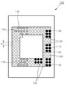
도 1은 본 발명 개념의 제 1 실시예에 따른 반도체 패키지(100)를 나타낸 평면도이다. 도 1을 참조하면, 반도체 패키지(100)의 표면에 메인 단자들(110)이 일정한 간격 d로 배치되어 있다. 상기 반도체 패키지는 에폭시 몰딩 컴파운드(EMC)와 같은 몰딩 수지로 몰딩된 반도체 패키지일 수도 있고, 칩스케일 패키지(CSP)를 위한 베어 다이(bare die)일 수도 있다. 또한, 인쇄 회로 기판에 반도체 다이가 실장된 것일 수도 있다.1 is a plan view showing a
도 1에 나타낸 메인 단자들(110)은 실질적으로 일정한 간격 d로 배열될 수 있다. 도 1에서는 상기 간격 d는 인접하는 메인 단자들(110)의 중심 사이의 거리로 정의하였지만, 상기 간격은 필요에 따라 인접하는 단자와 단자 사이의 피치(pitch)로 정의될 수도 있고, 인접하는 두 단자가 전기적으로 단락되게 할 수 있는 도체의 최단 길이로 정의될 수도 있다. 또한, 상기 간격 d가 "실질적으로" 일정하다는 것은 제조상의 공차(tolerance)로 인하여 발생하는 단자들 간의 각 간격들 사이의 차이는 무시됨을 의미한다.The
도 1에서는 상기 메인 단자들(110)이 원형으로 도시되었지만 반드시 원형일 필요는 없고 삼각형, 사각형, 오각형 등과 같은 임의의 다각형, 타원형 등일 수 있다. 다만, 상기 간격을 정의하기 위하여 각 단자의 형태와 배향이 일정한 것이 바람직하다.Although the
상기 메인 단자들(110)은 핀(pin) 또는 패드(pad) 등일 수 있으며, 패드인 경우에는 외부 장치와의 커넥션을 위하여 솔더볼(solder ball) 등과 같은 연결 부재가 더 구비될 수 있다. 상기 연결 부재는 당 기술분야에서 통상의 지식을 가진 자에게 잘 알려져 있으므로 여기서는 상세한 설명을 생략한다.The
상기 메인 단자들(110)은 정사각형 또는 직사각형의 외연을 갖도록 배열될 수 있다. 상기 메인 단자들(110)의 외연은 메인 단자들(110) 중 가장 바깥쪽에 위치하는 단자들 중 이웃하는 두 단자에 외접하는 선들에 의하여 정의되는 도형으로 정의한다. 도 1에서 보는 바와 같이 상기 메인 단자들(110)의 외연은 메인 단자 영역(110R)을 정의할 수 있다. 만일 도 1에 나타낸 것과는 달리 도 2에 나타낸 것처럼 메인 단자들(110) 중 가장 바깥쪽에 위치하는 단자들 중의 일부가 없는 경우에는 그 외연 (112R)에 일부 리세스 부분이 발생하므로 정사각형 또는 직사각형이 아닌 것으로 정의한다.The
도 1에서는 메인 단자들(110)의 외연(110R로 표시)이 정사각형을 정의하는 경우를 나타내었지만 직사각형일 수도 있다. 여기서 직사각형은 네 내각이 모두 직각인 사각형으로 정의된다. 따라서, 임의의 꼭지점에서 이웃하는 두 변의 길이는 서로 상이할 수 있다.Although FIG. 1 shows a case where the outer edge (denoted by 110R) of the
상기 메인 단자들(110)은 테스트 신호가 입력될 수 있는 복수의 입출력 단자들로 구성되는 제 1 세트(130)의 단자들(132)을 포함할 수 있다. 상기 제 1 세트(130)의 단자들(132)은 상기 반도체 패키지(100)의 정상 동작 시에는 데이터의 입출력이 없고 상기 반도체 패키지(100)를 테스트하는 동안에만 데이터의 입출력이 있을 수 있다. 다시 말해, 상기 제 1 세트(130)의 단자들(132)은 상기 반도체 패키지(100)를 테스트하는 동안에만 이용되는 것일 수 있다.The
상기 반도체 패키지(100)를 테스트하기 위하여, 테스트 장비의 테스트 프로브(미도시)는 상기 제 1 세트(130)의 단자들(132)과 전기적으로 연결되며, 상기 테스트 프로브는 상기 제 1 세트(130)의 단자들(132)을 통하여 상기 반도체 패키지(100)와 전기적으로 연결되어 테스트를 수행한다. 상기 테스트는 내부 동작을 확인할 수 있는 디버그(debug) 테스트일 수도 있고, 내부 상태를 확인할 수 있는 덤프(dump) 테스트일 수도 있다. 이러한 테스트를 수행할 수 있는 소정의 신호는 제조사, 제품의 종류, 제품의 규격 등에 따라 달라질 수 있으며, 당 기술분야에서 통상의 지식을 가진 자는 이러한 일련의 신호를 필요에 따라 스스로 창안할 수 있을 것이다.In order to test the
또한, 상기 테스트를 수행하기 위하여 상기 제 1 세트(130)의 단자들(132)을 통하여 테스트 모드를 온(on)시킬 수 있는 소정의 신호가 입력될 수 있다. 상기 테스트 모드를 온(on)시킬 수 있는 소정의 신호는 제조사, 제품의 종류, 제품의 규격 등에 따라 달라질 수 있으며, 당 기술분야에서 통상의 지식을 가진 자는 이러한 일련의 신호를 필요에 따라 스스로 창안할 수 있을 것이다.In order to perform the test, a predetermined signal capable of turning on the test mode through the
또한, 상기 테스트를 수행하기 위하여 상기 제 1 세트(130)의 단자들(132)을 통하여 테스트 모드를 오프(off)시킬 수 있는 소정의 신호가 입력될 수 있다. 상기 테스트 모드를 오프(off)시킬 수 있는 소정의 신호는 제조사, 제품의 종류, 제품의 규격 등에 따라 달라질 수 있으며, 당 기술분야에서 통상의 지식을 가진 자는 이러한 일련의 신호를 필요에 따라 스스로 창안할 수 있을 것이다.In order to perform the test, a predetermined signal capable of turning off the test mode through the
상기 제 1 세트(130)의 단자들(132)은 도 1에 나타낸 바와 같이 하나의 영역에 상호 인접하여 배치될 수도 있고, 도 4에 나타낸 바와 같이 둘 이상의 영역에 분산되어 배치될 수도 있다.The
상기 메인 단자들(110)은 상기 테스트 신호 이외의 신호가 입출력될 수 있는 복수의 입출력 단자들로 구성되는 제 2 세트(140)의 단자들(142)을 포함할 수 있다. 상기 테스트 신호 이외의 신호는 상기 반도체 패키지(100)의 정상 동작을 위한 신호를 포함한다. The
또한, 상기 메인 단자들(110)은 상기 반도체 패키지(100)의 테스트나 정상 동작과는 무관한 유보된(reserved) 단자들인 더미 단자(dummy terminal)들(150)을 포함할 수 있다.Also, the
또한, 상기 복수의 메인 패드들(110)의 외연을 이루는 직사각형 또는 정사각형의 네 변은 상기 반도체 패키지(100)의 네 변과 각각 평행할 수 있다.In addition, the four sides of the rectangle or square forming the outer edges of the plurality of
도 1에 나타낸 바와 같이, 상기 메인 단자들(110)은 외연을 이루는 상기 직사각형 또는 정사각형의 네 변을 따라 격자 배열될 수 있다. 상기 메인 단자들(110) 중 가장 바깥쪽에 위치하는 메인 단자들(110)은 상기 직사각형 또는 정사각형의 네 변을 따라 실질적으로 일정한 간격으로 배열되고, 이들로부터 상기 네 변에 평행한 방향으로 연장되는 선들의 교차점에 나머지 메인 단자들(110)이 위치함으로써 격자 배열될 수 있다.As shown in FIG. 1, the
한편, 상기 반도체 패키지(100)는 상기 직사각형 또는 정사각형의 내부에 상기 메인 단자들(110)이 배치되지 않은 블랭크 영역(120)을 포함할 수 있다. 상기 블랭크 영역(120)은 상기 메인 단자들(110)의 배열의 외연에 의하여 정의되는 정사각형 또는 직사각형 내에 존재할 수도 있고, 존재하지 않을 수도 있다.Meanwhile, the
상기 블랭크 영역(120)은 단자가 없는 영역을 의미하는 것이 아니라 메인 단자가 배치되지 않은 영역을 의미한다. 그러므로, 상기 블랭크 영역(120)에는 메인 단자들(110)이 아닌 엑스트라(extra) 단자가 배치될 수 있다.The
상기 블랭크 영역(120)은, 만일 존재한다면, 상기 정사각형 또는 직사각형 내에서 상기 메인 단자들(110)이 존재하지 않는 영역(즉, 블랭크 영역)에서 가장 가까운 메인 단자들(110) 중 이웃하는 두 단자에 접하는 선들, 특히 상기 메인 단자들(110)이 존재하지 않는 쪽에서 접하는 선들에 의하여 정의되는 도형으로 정의될 수 있다.The
도 3을 참조하면, 단자(193)는 주변의 단자들과 균일한 간격으로 배열되어 있기 때문에 메인 단자(110)의 일부로서 간주될 수 있다. 그러나, 단자(191)는 주변의단자들과의 간격이 다른 단자들 사이의 간격과 동일하지 않기 때문에 메인 단자(110)에 포함되는 것으로 볼 수 없다. 따라서, 도 3에서 (120)으로 표시된 영역은 블랭크 영역(120)으로 볼 수 있고 여기에 속하는 단자인 단자(191)는 엑스트라 단자로서 간주될 수 있다.Referring to FIG. 3, the terminal 193 may be regarded as a part of the
도 1 내지 도 4에서는 메인 단자(110)들이 배열된 메인 단자 영역(110R) 한가운데에 블랭크 영역(120)이 배치된 경우를 도시하였지만, 상기 블랭크 영역(120)이 반드시 메인 단자 영역(110R)의 가운데에 배치될 필요는 없고 어느 한 쪽으로 치우쳐서 존재할 수도 있다. 그러나, 앞서 언급한 바와 같이 상기 블랭크 영역(120)을 정의할 수 있도록 상기 블랭크 영역(120)은 메인 단자들(110)에 의하여 둘러싸여야 한다.1 to 4 show a case where the
본 발명 개념의 제 2 실시예는 표면에 복수의 메인 단자들이 배열된 반도체 패키지 단자로서, 상기 메인 단자들이 배열된 외연이 직사각형 또는 정사각형을 갖는다. 특히, 상기 반도체 패키지를 테스트하기 위한 테스트 신호가 입력될 수 있는 복수의 입출력 단자들로 구성되는 제 1 세트의 단자들을 갖는데, 상기 제 1 세트의 단자들의 적어도 일부가 상기 직사각형 또는 정사각형 내에 위치할 수 있다. A second embodiment of the present invention concept is a semiconductor package terminal in which a plurality of main terminals are arranged on a surface, wherein the outer rim in which the main terminals are arranged has a rectangular shape or a square shape. In particular, there is a first set of terminals comprising a plurality of input / output terminals into which a test signal for testing the semiconductor package may be input, wherein at least a portion of the terminals of the first set may be located within the rectangle or square have.
도 5는 본 발명 개념의 제 2 실시예에 따른 반도체 패키지(200)를 나타낸 평면도이다. 간결한 설명을 위하여 제 1 실시예와 중복되는 사항에 대해서는 상세한 설명을 생략한다.5 is a plan view showing a
도 5를 참조하면, 반도체 패키지(200)의 표면에 메인 단자들(210)이 일정한 간격 d로 배치되어 있다. 도 1에서와 유사하게, 상기 메인 단자들(210)이 배열된 메인 단자 영역(210R)의 외연은 정사각형을 이루고 있는데, 정사각형에 한정되지 않고 직사각형일 수도 있다.Referring to FIG. 5, the
제 1 실시예에서와 유사하게 상기 반도체 패키지(200)는 블랭크 영역(220)을 포함할 수 있다. 상기 블랭크 영역(220)의 정의와 관련하여서는 제 1 실시예의 설명 부분에서 설명하였으므로 여기서는 생략한다.Similar to the first embodiment, the
상기 블랭크 영역(220) 내에는 하나 이상의 제 1 엑스트라 단자(들)(260)을 포함할 수 있다. 상기 제 1 엑스트라 단자(들)(260)은 상기 메인 단자들(210)이 배열된 간격과 상이한 간격을 메인 단자들(210)과 가지며, 상기 블랭크 영역(220) 내에 임의로 배열될 수 있다.The
앞서 제 1 실시예에서 설명한 바와 같이 제 1 세트(230)의 단자들(232)은 테스트 신호가 입력될 수 있는 복수의 입출력 단자들로 구성될 수 있다. 테스트 신호에 대해서는 제 1 실시예에서 설명하였으므로 여기서는 상세한 설명을 생략한다.As described in the first embodiment, the
또한, 제 2 세트(240)의 단자들(242)은 테스트 신호 이외의 신호가 입출력될 수 있는 복수의 입출력 단자들로 구성될 수 있다. 상기 테스트 신호 이외의 신호는 상기 반도체 패키지(200)의 정상 동작을 위한 신호를 포함한다.In addition, the
상기 메인 단자들(110)과 상기 제 1 엑스트라 단자(들)(260)은 상기 제 1 세트(230)의 단자들(232)을 포함할 수 있다. 또한, 상기 메인 단자들(210)과 상기 제 1 엑스트라 단자(들)(260)은 상기 제 2 세트(240)의 단자들(242)을 포함할 수 있다.The
상기 제 1 세트(230)의 단자들(232)은 모두 메인 단자들(210) 내에 포함될 수도 있지만, 도 6에 나타낸 바와 같이 상기 제 1 세트(230)의 단자들(232)의 적어도 일부분은 상기 제 1 엑스트라 단자(들)(260)에 속할 수도 있다. 마찬가지로, 제 2 세트(240)의 단자들(242)은 모두 메인 단자들(210) 내에 포함될 수도 있지만, 상기 제 2 세트(240)의 단자들(242)의 적어도 일부분은 상기 제 1 엑스트라 단자(들)(260)에 속할 수도 있다. 나아가, 상기 제 1 세트(230)의 단자들(232)의 전부가 상기 제 1 엑스트라 단자(들)(260)에 속할 수도 있다. 또한, 상기 제 2 세트(240)의 단자들(242)의 전부가 상기 제 1 엑스트라 단자(들)(260)에 속할 수도 있다.The
또한, 상기 메인 단자들(210) 및/또는 상기 제 1 엑스트라 단자(들)(260)은 더미 단자들(250)을 포함할 수 있다. 상기 더미 단자들(250)은 상기 반도체 패키지(200)의 테스트나 정상동작과는 무관한 유보된 단자들일 수 있다.Also, the
본 발명 개념의 제 3 실시예는 제 2 엑스트라 단자들을 갖는 점을 제외하면 상기 제 2 실시예와 유사하며 도 7을 참조하여 설명한다. 도 7은 본 발명 개념의 제 3 실시예에 따른 반도체 패키지(300)를 나타낸 평면도이며 간결한 설명을 위하여 제 1 실시예 및 제 2 실시예와 중복되는 사항에 대해서는 상세한 설명을 생략한다.A third embodiment of the inventive concept is similar to the second embodiment except that it has second extra terminals and will be described with reference to Fig. FIG. 7 is a plan view of a
도 7을 참조하면, 반도체 패키지(300)의 표면에 메인 단자들(310)이 일정한 간격 d로 배치되어 있다. 상기 메인 단자들(310)이 배열된 메인 단자 영역(310R)의 외연은 정사각형 또는 직사각형일 수 있다.Referring to FIG. 7,
또한, 상기 반도체 패키지(300)는 블랭크 영역(320)을 포함할 수 있으며, 상기 블랭크 영역(320) 내에는 하나 이상의 제 1 엑스트라 단자(들)(360)이 구비될 수 있다. 상기 제 1 엑스트라 단자(들)(360)은 상기 메인 단자들(310)이 배열된 간격과 상이한 간격을 상기 메인 단자들(310)과의 사이에 가지며, 상기 블랭크 영역(320) 내에 임의로 배열될 수 있다.The
또한, 상기 반도체 패키지(300)는 상기 직사각형 또는 정사각형의 외부에 하나 이상의 제 2 엑스트라 단자(들)(370)을 구비할 수 있다. 상기 제 2 엑스트라 단자(들)(370)은 상기 메인 단자들(310)이 배열된 간격과 상이한 간격을 상기 메인 단자들(310)과의 사이에 가지며, 상기 직사각형 또는 정사각형의 외부에 임의로 배열될 수 있다.In addition, the
제 1 세트(330)의 단자들(332)은 테스트 신호가 입력될 수 있는 복수의 입력 및/또는 출력 단자들로 구성될 수 있다. 앞서 설명한 바와 같이 제 1 세트(330)의 단자들(332)은 모두 메인 단자들(310) 내에 포함될 수도 있고, 또는 제 1 세트(330)의 단자들(332)의 일부 또는 전부가 제 1 엑스트라 단자(들)(360)에 포함될 수 있다. 또한, 제 1 세트(330)의 단자들(332)의 일부 또는 전부가 제 2 엑스트라 단자(들)(370)에 포함될 수 있다.The
또, 제 2 세트(340)의 단자들(342)은 테스트 신호 이외의 신호가 입출력될 수 있는 하나 이상의 입출력 단자들로 구성될 수 있다. 앞서 설명한 바와 같이 제 2 세트(340)의 단자들(342)은 모두 메인 단자들(310) 내에 포함될 수도 있고, 또는 제 2 세트(340)의 단자들(342)의 일부 또는 전부가 제 1 엑스트라 단자(들)(360)에 포함될 수 있다. 또한, 제 2 세트(340)의 단자들(342)의 일부 또는 전부가 제 2 엑스트라 단자(들)(370)에 포함될 수 있다.In addition, the
도 8은 본 발명 개념의 기술적 사상에 의한 일 실시예에 따른 메모리 모듈(800)을 보여주는 개략도이다.FIG. 8 is a schematic diagram illustrating a
도 8을 참조하면, 제어기(810)와 메모리(820)는 전기적인 신호를 교환하도록 배치될 수 있다. 예를 들어, 제어기(810)에서 명령을 내리면, 메모리(820)는 데이터를 전송할 수 있다. 메모리(820)는 본 발명 개념의 실시예들 중 어느 하나에 따른 반도체 패키지를 메모리 소자로서 포함할 수 있다. 본 발명 개념의 다양한 실시예들에 따른 반도체 패키지에 포함된 상기 메모리 소자들은 당해 기술 분야에서 잘 알려진 바와 같이 휘발성 또는 비휘발성 메모리 소자들일 수 있고, 예를 들면 "NAND" 또는 "NOR" 아키텍쳐 메모리 소자일 수 있다. 복수의 행과 열로 배치된 "NAND" 또는 "NOR" 아키텍처 메모리 어레이는 하나 이상의 메모리 어레이 뱅크(미도시)를 구성할 수 있다. 메모리(820)은 이러한 메모리 어레이(미도시) 또는 메모리 어레이 뱅크(미도시)를 포함할 수 있다. 또한, 메모리 모듈(800)은 상술한 메모리 어레이 뱅크(미도시)를 구동하기 위하여 통상의 행디코더(미도시), 열디코더(미도시), I/O 버퍼들(미도시), 및/또는 제어 레지스터(미도시)가 더 포함할 수 있다. 이러한 메모리 모듈(800)은 다양한 종류의 멀티칩 패키지(MCP: multi-chip packages), 임베디드 멀티미디어 카드(eMMC: embedded multimedia card) 등의 퓨전 메모리들을 포함할 수 있다.8, the
도 9는 본 발명 개념의 기술적 사상에 의한 일 실시예에 따른 시스템(900)을 보여주는 개략도이다.FIG. 9 is a schematic diagram illustrating a
도 9를 참조하면, 상기 시스템(900)은 제어기(910), 입/출력 장치(930), 메모리 모듈(920) 및 인터페이스(940)을 포함할 수 있다. 상기 시스템(900)은 모바일 시스템 또는 정보를 전송하거나 전송받는 시스템일 수 있다. 상기 모바일 시스템은 PDA, 휴대용 컴퓨터(portable computer), 웹 타블렛(web tablet), 무선 폰(wireless phone), 모바일 폰(mobile phone), 디지털 뮤직 플레이어(digital music player) 또는 메모리 카드(memory card)일 수 있다. 제어기(910)는 프로그램을 실행하고, 시스템(900)을 제어하는 역할을 할 수 있다. 제어기(910)는, 예를 들어 마이크로프로세서(microprocessor), 디지털 신호 처리기(digital signal processor), 마이크로콘트롤러(microcontroller) 또는 이와 유사한 장치일 수 있다. 입/출력 장치(930)는 시스템(900)의 데이터를 입력 또는 출력하는데 이용될 수 있다. 시스템(900)은 입/출력 장치(930)를 이용하여 외부 장치, 예컨대 개인용 컴퓨터 또는 네트워크에 연결되어, 외부 장치와 서로 데이터를 교환할 수 있다. 입/출력 장치(930)는, 예를 들어 키단자(keypad), 키보드(keyboard) 또는 표시장치(display)일 수 있다. 메모리 모듈(920)은 제어기(910)의 동작을 위한 코드 및/또는 데이터를 저장하거나, 및/또는 제어기(910)에서 처리된 데이터를 저장할 수 있다. 상기 메모리 모듈(920)은 본 발명 개념의 실시예들 중 어느 하나에 따른 반도체 패키지를 포함할 수 있다. 인터페이스(940)는 상기 시스템(900)과 외부의 다른 장치 사이의 데이터 전송통로일 수 있다. 제어기(910), 입/출력 장치(930), 메모리(920) 및 인터페이스(340)는 버스(950)를 통하여 서로 통신할 수 있다. 예를 들어, 이러한 시스템(900)은 모바일 폰(mobile phone), MP3 플레이어, 네비게이션(navigation), 휴대용 멀티미디어 재생기(portable multimedia player, PMP), 고상 디스크(solid state disk, SSD) 또는 가전 제품(household appliances)에 이용될 수 있다.9, the
이상에서 설명한 것은 본 발명 개념의 예시이고, 본 발명 개념을 한정하는 것으로 해석되어서는 안된다. 비록 본 발명 개념의 몇몇 예시적 실시예들이 개시되었지만, 당 기술 분야에서 통상의 지식을 가진 자는 본 발명 개념의 새로운 가르침과 장점으로부터 실질적으로 이탈하지 않으면서 상기 예시적 실시예들에 수많은 변경이 가해질 수 있음을 이해할 것이다. 따라서, 그러한 모든 변경들은 청구항에 정의된 바와 같은 본 발명 개념의 범위 내에 포함되도록 의도된다. 그러므로, 이상에서 설명한 것은 본 발명 개념의 예시이고, 개시된 구체적 실시예에 한정되는 것으로 해석되어서는 아니되며, 다른 실시예들 뿐만 아니라 개시된 실시예들에 대한 변경은 첨부된 청구항의 범위 내에 포함되도록 의도됨은 이해될 것이다. 본 발명 개념은 이하의 청구항과 여기에 포함된 청구항들의 균등 범위에 의하여 정의된다.What has been described above is an example of the concept of the present invention and should not be construed as limiting the concept of the present invention. Although several exemplary embodiments of the inventive concept have been disclosed, those skilled in the art will readily recognize that many changes can be made to the illustrative embodiments without departing substantially from the novel teachings and advantages of the inventive concept It will be understood. Accordingly, all such modifications are intended to be included within the scope of the inventive concept as defined in the claims. Therefore, it should be understood, therefore, that the foregoing is illustrative of the concept of the invention and should not be construed as limited to the specific embodiments disclosed, and that modifications to the disclosed embodiments as well as other embodiments are intended to be included within the scope of the appended claims. Will be understood. The inventive concept is defined by the following claims and the equivalents of the claims included therein.
본 발명은 반도체 산업 분야에 유용하다.The present invention is useful in the semiconductor industry.
100, 200, 300: 반도체 패키지
110, 210, 310: 메인 단자
110R, 210R, 310R: 메인 단자 영역
120, 220, 320: 블랭크 영역
130, 230, 330: 제 1 세트
132, 232, 332: 제 1 세트의 단자
140, 240, 340: 제 2 세트
142, 242, 342: 제 2 세트의 단자
150, 250, 350: 더미 패드
260, 360: 제 1 엑스트라 패드
370: 제 2 엑스트라 패드100, 200, 300: semiconductor package
110, 210, 310: main terminal
110R, 210R, 310R: Main terminal area
120, 220, 320: blank area
130, 230, 330: a first set
132, 232, 332: a first set of terminals
140, 240, 340: the second set
142, 242, 342: a second set of terminals
150, 250, 350: dummy pad
260, 360: First Extra Pad
370: Second Extra Pad
Claims (22)
상기 복수의 메인 단자들은,
테스트 신호가 입력될 수 있는 복수의 입출력 단자들로 구성되는 제 1 세트의 단자들의 적어도 일부; 및
상기 테스트 신호 이외의 신호가 입출력될 수 있는 복수의 입출력 단자들로 구성되는 제 2 세트의 단자들의 적어도 일부;
을 포함하고,
상기 복수의 메인 단자들은 메인 단자 영역 내에서 일정한 제 1 간격으로 배열되고,
상기 메인 단자 영역 외의 영역에서 일정한 제 2 간격으로 배치된 엑스트라 단자들은 상기 제 1 세트의 단자들 중의 하나 이상과 상기 제 2 세트의 단자들 중의 하나 이상을 포함하고,
상기 엑스트라 단자들과 상기 메인 단자 영역에 배열된 단자 사이의 간격은 상기 제 1 간격과 상이한 반도체 패키지.A plurality of main terminals are arranged on the surface at regular intervals,
The plurality of main terminals may include:
At least a portion of a first set of terminals comprising a plurality of input / output terminals into which a test signal can be input; And
At least a part of a second set of terminals constituted by a plurality of input / output terminals through which a signal other than the test signal can be input / output;
/ RTI >
Wherein the plurality of main terminals are arranged at a first interval in the main terminal region,
Extraneous terminals disposed at a constant second interval in an area outside the main terminal area include at least one of the first set of terminals and the second set of terminals,
Wherein an interval between the extra terminals and a terminal arranged in the main terminal region is different from the first interval.
테스트 신호가 입력될 수 있는 복수의 입출력 단자들로 구성되는 제 1 세트의 단자들의 적어도 일부 및 상기 테스트 신호 이외의 신호가 입출력될 수 있는 복수의 입출력 단자들로 구성되는 제 2 세트의 단자들의 적어도 일부를 상기 직사각형 또는 정사각형 내에 포함하고,
상기 직사각형 또는 정사각형의 내부에 상기 메인 단자들이 배치되지 않은 블랭크 영역을 포함하고,
상기 블랭크 영역 내에 배치된 엑스트라 단자들은 상기 제 1 세트의 단자들 중의 하나 이상과 상기 제 2 세트의 단자들 중의 하나 이상을 포함하고,
상기 엑스트라 단자와 상기 메인 단자 사이의 거리는 상기 제 1 간격과 상이한 반도체 패키지.A plurality of main terminals arranged at a constant first interval so as to have an outer edge of a rectangle or a square,
At least a part of a first set of terminals constituted by a plurality of input / output terminals into which a test signal can be input and a plurality of input / output terminals through which a signal other than the test signal can be input / A part of which is contained in said rectangle or square,
And a blank region in which the main terminals are not disposed inside the rectangle or square,
Wherein extraneous terminals disposed in the blank region include at least one of the first set of terminals and the second set of terminals,
Wherein the distance between the extra terminal and the main terminal is different from the first distance.
데이터를 입력 또는 출력할 수 있는 입출력부;
데이터를 저장할 수 있는 메모리부;
외부 장치와 데이터를 전송할 수 있는 인터페이스부; 및
상기 제어부, 입출력부, 메모리부 및 인터페이스부를 서로 통신 가능하도록 연결하는 버스;
를 포함하는 전자 시스템으로서,
상기 메모리부가 제 21 항에 따른 반도체 메모리 모듈을 포함하는 전자 시스템.A control unit;
An input / output unit capable of inputting or outputting data;
A memory unit capable of storing data;
An interface unit capable of transmitting data with an external device; And
A bus connecting the control unit, the input / output unit, the memory unit, and the interface unit so that they can communicate with each other;
The electronic system comprising:
Wherein the memory section comprises the semiconductor memory module according to claim 21.
Priority Applications (2)
| Application Number | Priority Date | Filing Date | Title |
|---|---|---|---|
| KR1020100053989A KR101744756B1 (en) | 2010-06-08 | 2010-06-08 | Semiconductor packages |
| US13/118,948 US8618540B2 (en) | 2010-06-08 | 2011-05-31 | Semiconductor packages |
Applications Claiming Priority (1)
| Application Number | Priority Date | Filing Date | Title |
|---|---|---|---|
| KR1020100053989A KR101744756B1 (en) | 2010-06-08 | 2010-06-08 | Semiconductor packages |
Publications (2)
| Publication Number | Publication Date |
|---|---|
| KR20110134157A KR20110134157A (en) | 2011-12-14 |
| KR101744756B1 true KR101744756B1 (en) | 2017-06-09 |
Family
ID=45063780
Family Applications (1)
| Application Number | Title | Priority Date | Filing Date |
|---|---|---|---|
| KR1020100053989A Active KR101744756B1 (en) | 2010-06-08 | 2010-06-08 | Semiconductor packages |
Country Status (2)
| Country | Link |
|---|---|
| US (1) | US8618540B2 (en) |
| KR (1) | KR101744756B1 (en) |
Families Citing this family (2)
| Publication number | Priority date | Publication date | Assignee | Title |
|---|---|---|---|---|
| CN105789065B (en) | 2016-04-08 | 2019-02-12 | Oppo广东移动通信有限公司 | Chip packaging structure, terminal equipment and method |
| JP1664282S (en) * | 2019-07-24 | 2020-07-27 |
Citations (1)
| Publication number | Priority date | Publication date | Assignee | Title |
|---|---|---|---|---|
| US20090101896A1 (en) * | 2007-10-23 | 2009-04-23 | Masatoshi Shinagawa | Semiconductor device |
Family Cites Families (16)
| Publication number | Priority date | Publication date | Assignee | Title |
|---|---|---|---|---|
| JP3179420B2 (en) * | 1998-11-10 | 2001-06-25 | 日本電気株式会社 | Semiconductor device |
| US6198635B1 (en) * | 1999-05-18 | 2001-03-06 | Vsli Technology, Inc. | Interconnect layout pattern for integrated circuit packages and the like |
| US6512289B1 (en) * | 2000-05-09 | 2003-01-28 | Xilinx, Inc. | Direct current regulation on integrated circuits under high current design conditions |
| KR20020045641A (en) | 2000-12-09 | 2002-06-20 | 박종섭 | Semiconductor device |
| JP2003204030A (en) * | 2002-01-07 | 2003-07-18 | Hitachi Ltd | Semiconductor device and method of manufacturing the same |
| JP2003249558A (en) | 2002-02-22 | 2003-09-05 | Seiko Instruments Inc | Semiconductor chip |
| JP3657246B2 (en) * | 2002-07-29 | 2005-06-08 | Necエレクトロニクス株式会社 | Semiconductor device |
| JP4674850B2 (en) * | 2005-02-25 | 2011-04-20 | ルネサスエレクトロニクス株式会社 | Semiconductor device |
| JP2006344824A (en) * | 2005-06-09 | 2006-12-21 | Nec Electronics Corp | Semiconductor device and manufacturing method of semiconductor device |
| US20070070672A1 (en) * | 2005-09-29 | 2007-03-29 | Hynix Semiconductor Inc. | Semiconductor device and driving method thereof |
| KR100804148B1 (en) | 2005-09-29 | 2008-02-19 | 주식회사 하이닉스반도체 | Semiconductor device |
| KR101131138B1 (en) * | 2006-01-04 | 2012-04-03 | 삼성전자주식회사 | Substrate having ball pad of various size, semiconductor package having the same and stack package using the semiconductor package |
| JP5222509B2 (en) * | 2007-09-12 | 2013-06-26 | ルネサスエレクトロニクス株式会社 | Semiconductor device |
| JP4862017B2 (en) * | 2008-07-10 | 2012-01-25 | ルネサスエレクトロニクス株式会社 | Relay board, manufacturing method thereof, probe card |
| JP4343256B1 (en) * | 2008-07-10 | 2009-10-14 | Necエレクトロニクス株式会社 | Manufacturing method of semiconductor device |
| JP2010093109A (en) * | 2008-10-09 | 2010-04-22 | Renesas Technology Corp | Semiconductor device, method of manufacturing the same, and method of manufacturing semiconductor module |
-
2010
- 2010-06-08 KR KR1020100053989A patent/KR101744756B1/en active Active
-
2011
- 2011-05-31 US US13/118,948 patent/US8618540B2/en active Active
Patent Citations (1)
| Publication number | Priority date | Publication date | Assignee | Title |
|---|---|---|---|---|
| US20090101896A1 (en) * | 2007-10-23 | 2009-04-23 | Masatoshi Shinagawa | Semiconductor device |
Also Published As
| Publication number | Publication date |
|---|---|
| US8618540B2 (en) | 2013-12-31 |
| US20110297933A1 (en) | 2011-12-08 |
| KR20110134157A (en) | 2011-12-14 |
Similar Documents
| Publication | Publication Date | Title |
|---|---|---|
| KR102144367B1 (en) | Semiconductor package and method of fabricating the same | |
| US8611123B2 (en) | Complex semiconductor device for use in mobile equipment | |
| US9559079B2 (en) | Semiconductor stack packages | |
| KR20130044048A (en) | Semiconductor wafer and method for fabricating stack package using the same | |
| US20180150676A1 (en) | Biometric sensing chip and electronic device using same | |
| CN111524879B (en) | Semiconductor package having stacked chip structure | |
| US8680524B2 (en) | Method of arranging pads in semiconductor device, semiconductor memory device using the method, and processing system having mounted therein the semiconductor memory device | |
| KR20210040531A (en) | Semiconductor device and stacked semiconductor package using wire | |
| US11107795B2 (en) | Semiconductor devices with duplicated die bond pads and associated device packages and methods of manufacture | |
| KR101744756B1 (en) | Semiconductor packages | |
| JP6761180B2 (en) | Semiconductor device | |
| US7843226B2 (en) | Semiconductor integrated circuit device and test terminal arrangement method | |
| US20140070407A1 (en) | Semiconductor package and method of fabricating the same | |
| JP2007096071A (en) | Semiconductor memory card | |
| KR101273411B1 (en) | Semiconductor module | |
| CN104425000A (en) | Memory Structure of Sequential Serial Multi-chip | |
| CN108695268B (en) | Wafer level package, semiconductor device unit and manufacturing method thereof | |
| JP2003318353A (en) | Semiconductor chip package | |
| US9041222B2 (en) | Semiconductor device | |
| US8159831B2 (en) | Printed circuit board for accomplishing narrow scribe lane and semiconductor package including the printed circuit board | |
| US20150189750A1 (en) | Package substrates and integrated circuit packages including the same | |
| KR100791003B1 (en) | Terminal arrangement method in semiconductor memory module and semiconductor memory module | |
| US20240347498A1 (en) | Memory devices, and semiconductor packages including the same | |
| US20160284791A1 (en) | Capacitor and semiconductor device including the same | |
| US20070018691A1 (en) | Multi-pad structure for semiconductor device |
Legal Events
| Date | Code | Title | Description |
|---|---|---|---|
| PA0109 | Patent application |
St.27 status event code: A-0-1-A10-A12-nap-PA0109 |
|
| PG1501 | Laying open of application |
St.27 status event code: A-1-1-Q10-Q12-nap-PG1501 |
|
| R18-X000 | Changes to party contact information recorded |
St.27 status event code: A-3-3-R10-R18-oth-X000 |
|
| A201 | Request for examination | ||
| E13-X000 | Pre-grant limitation requested |
St.27 status event code: A-2-3-E10-E13-lim-X000 |
|
| P11-X000 | Amendment of application requested |
St.27 status event code: A-2-2-P10-P11-nap-X000 |
|
| P13-X000 | Application amended |
St.27 status event code: A-2-2-P10-P13-nap-X000 |
|
| PA0201 | Request for examination |
St.27 status event code: A-1-2-D10-D11-exm-PA0201 |
|
| P22-X000 | Classification modified |
St.27 status event code: A-2-2-P10-P22-nap-X000 |
|
| D13-X000 | Search requested |
St.27 status event code: A-1-2-D10-D13-srh-X000 |
|
| D14-X000 | Search report completed |
St.27 status event code: A-1-2-D10-D14-srh-X000 |
|
| E902 | Notification of reason for refusal | ||
| PE0902 | Notice of grounds for rejection |
St.27 status event code: A-1-2-D10-D21-exm-PE0902 |
|
| E13-X000 | Pre-grant limitation requested |
St.27 status event code: A-2-3-E10-E13-lim-X000 |
|
| P11-X000 | Amendment of application requested |
St.27 status event code: A-2-2-P10-P11-nap-X000 |
|
| P13-X000 | Application amended |
St.27 status event code: A-2-2-P10-P13-nap-X000 |
|
| E90F | Notification of reason for final refusal | ||
| PE0902 | Notice of grounds for rejection |
St.27 status event code: A-1-2-D10-D21-exm-PE0902 |
|
| P11-X000 | Amendment of application requested |
St.27 status event code: A-2-2-P10-P11-nap-X000 |
|
| P13-X000 | Application amended |
St.27 status event code: A-2-2-P10-P13-nap-X000 |
|
| PE0701 | Decision of registration |
St.27 status event code: A-1-2-D10-D22-exm-PE0701 |
|
| GRNT | Written decision to grant | ||
| PR0701 | Registration of establishment |
St.27 status event code: A-2-4-F10-F11-exm-PR0701 |
|
| PR1002 | Payment of registration fee |
St.27 status event code: A-2-2-U10-U11-oth-PR1002 Fee payment year number: 1 |
|
| PG1601 | Publication of registration |
St.27 status event code: A-4-4-Q10-Q13-nap-PG1601 |
|
| PR1001 | Payment of annual fee |
St.27 status event code: A-4-4-U10-U11-oth-PR1001 Fee payment year number: 4 |
|
| PR1001 | Payment of annual fee |
St.27 status event code: A-4-4-U10-U11-oth-PR1001 Fee payment year number: 5 |
|
| PR1001 | Payment of annual fee |
St.27 status event code: A-4-4-U10-U11-oth-PR1001 Fee payment year number: 6 |
|
| PR1001 | Payment of annual fee |
St.27 status event code: A-4-4-U10-U11-oth-PR1001 Fee payment year number: 7 |
|
| PR1001 | Payment of annual fee |
St.27 status event code: A-4-4-U10-U11-oth-PR1001 Fee payment year number: 8 |
|
| PR1001 | Payment of annual fee |
St.27 status event code: A-4-4-U10-U11-oth-PR1001 Fee payment year number: 9 |
|
| P22-X000 | Classification modified |
St.27 status event code: A-4-4-P10-P22-nap-X000 |