KR100791003B1 - Terminal arrangement method in semiconductor memory module and semiconductor memory module - Google Patents
Terminal arrangement method in semiconductor memory module and semiconductor memory module Download PDFInfo
- Publication number
- KR100791003B1 KR100791003B1 KR1020060115421A KR20060115421A KR100791003B1 KR 100791003 B1 KR100791003 B1 KR 100791003B1 KR 1020060115421 A KR1020060115421 A KR 1020060115421A KR 20060115421 A KR20060115421 A KR 20060115421A KR 100791003 B1 KR100791003 B1 KR 100791003B1
- Authority
- KR
- South Korea
- Prior art keywords
- semiconductor memory
- memory device
- terminals
- terminal
- predetermined terminals
- Prior art date
- Legal status (The legal status is an assumption and is not a legal conclusion. Google has not performed a legal analysis and makes no representation as to the accuracy of the status listed.)
- Expired - Fee Related
Links
Images


Classifications
-
- H—ELECTRICITY
- H05—ELECTRIC TECHNIQUES NOT OTHERWISE PROVIDED FOR
- H05K—PRINTED CIRCUITS; CASINGS OR CONSTRUCTIONAL DETAILS OF ELECTRIC APPARATUS; MANUFACTURE OF ASSEMBLAGES OF ELECTRICAL COMPONENTS
- H05K1/00—Printed circuits
- H05K1/18—Printed circuits structurally associated with non-printed electric components
- H05K1/181—Printed circuits structurally associated with non-printed electric components associated with surface mounted components
-
- G—PHYSICS
- G11—INFORMATION STORAGE
- G11C—STATIC STORES
- G11C7/00—Arrangements for writing information into, or reading information out from, a digital store
- G11C7/10—Input/output [I/O] data interface arrangements, e.g. I/O data control circuits, I/O data buffers
-
- G—PHYSICS
- G11—INFORMATION STORAGE
- G11C—STATIC STORES
- G11C5/00—Details of stores covered by group G11C11/00
- G11C5/02—Disposition of storage elements, e.g. in the form of a matrix array
- G11C5/025—Geometric lay-out considerations of storage- and peripheral-blocks in a semiconductor storage device
-
- G—PHYSICS
- G11—INFORMATION STORAGE
- G11C—STATIC STORES
- G11C5/00—Details of stores covered by group G11C11/00
- G11C5/02—Disposition of storage elements, e.g. in the form of a matrix array
- G11C5/04—Supports for storage elements, e.g. memory modules; Mounting or fixing of storage elements on such supports
-
- H—ELECTRICITY
- H05—ELECTRIC TECHNIQUES NOT OTHERWISE PROVIDED FOR
- H05K—PRINTED CIRCUITS; CASINGS OR CONSTRUCTIONAL DETAILS OF ELECTRIC APPARATUS; MANUFACTURE OF ASSEMBLAGES OF ELECTRICAL COMPONENTS
- H05K2201/00—Indexing scheme relating to printed circuits covered by H05K1/00
- H05K2201/09—Shape and layout
- H05K2201/09209—Shape and layout details of conductors
- H05K2201/09372—Pads and lands
- H05K2201/09418—Special orientation of pads, lands or terminals of component, e.g. radial or polygonal orientation
-
- H—ELECTRICITY
- H05—ELECTRIC TECHNIQUES NOT OTHERWISE PROVIDED FOR
- H05K—PRINTED CIRCUITS; CASINGS OR CONSTRUCTIONAL DETAILS OF ELECTRIC APPARATUS; MANUFACTURE OF ASSEMBLAGES OF ELECTRICAL COMPONENTS
- H05K2201/00—Indexing scheme relating to printed circuits covered by H05K1/00
- H05K2201/10—Details of components or other objects attached to or integrated in a printed circuit board
- H05K2201/10007—Types of components
- H05K2201/10159—Memory
-
- H10W90/00—
-
- Y—GENERAL TAGGING OF NEW TECHNOLOGICAL DEVELOPMENTS; GENERAL TAGGING OF CROSS-SECTIONAL TECHNOLOGIES SPANNING OVER SEVERAL SECTIONS OF THE IPC; TECHNICAL SUBJECTS COVERED BY FORMER USPC CROSS-REFERENCE ART COLLECTIONS [XRACs] AND DIGESTS
- Y02—TECHNOLOGIES OR APPLICATIONS FOR MITIGATION OR ADAPTATION AGAINST CLIMATE CHANGE
- Y02P—CLIMATE CHANGE MITIGATION TECHNOLOGIES IN THE PRODUCTION OR PROCESSING OF GOODS
- Y02P70/00—Climate change mitigation technologies in the production process for final industrial or consumer products
- Y02P70/50—Manufacturing or production processes characterised by the final manufactured product
Landscapes
- Engineering & Computer Science (AREA)
- Microelectronics & Electronic Packaging (AREA)
- Semiconductor Memories (AREA)
Abstract
본 발명은 반도체 메모리 모듈 및 반도체 메모리 모듈에서의 터미널 배치 방법에 관한 것으로서, 특히 반도체 메모리 모듈에서 각각의 스터브(stub) 길이를 최소화할 수 있는 기술에 관한 것이다. 제 1 반도체 메모리 소자와 제 2 반도체 메모리 소자를 구비하는 반도체 메모리 모듈에 있어서, 본 발명에 따른 반도체 메모리 모듈에서는, 상기 제 1 반도체 메모리 소자의 소정 터미널들은 상기 제 1 반도체 메모리 소자의 에지 영역들 중에서 상기 제 2 반도체 메모리 소자에 근접한 에지 영역에 배치되고, 상기 제 2 반도체 메모리 소자의 소정 터미널들은 상기 제 2 반도체 메모리 소자의 에지 영역들 중에서 상기 제 1 반도체 메모리 소자에 근접한 에지 영역에 배치되며, 상기 제 1 반도체 메모리 소자의 소정 터미널들과 상기 제 2 반도체 메모리 소자의 소정 터미널들은 서로 대칭이 되도록 배치된다.The present invention relates to a semiconductor memory module and a method for arranging terminals in a semiconductor memory module, and more particularly, to a technology capable of minimizing each stub length in a semiconductor memory module. A semiconductor memory module having a first semiconductor memory element and a second semiconductor memory element, wherein in the semiconductor memory module according to the present invention, predetermined terminals of the first semiconductor memory element are selected from edge regions of the first semiconductor memory element. Disposed in an edge region proximate to the second semiconductor memory element, and predetermined terminals of the second semiconductor memory element are disposed in an edge region proximate to the first semiconductor memory element among edge regions of the second semiconductor memory element, The predetermined terminals of the first semiconductor memory element and the predetermined terminals of the second semiconductor memory element are disposed to be symmetrical to each other.
Description
본 발명의 상세한 설명에서 인용되는 도면을 이해하기 위하여 각 도면에 대한 간단한 설명이 제공된다.BRIEF DESCRIPTION OF THE DRAWINGS In order to understand the drawings referred to in the detailed description of the invention, a brief description of each drawing is provided.
도 1a은 다수의 반도체 메모리 소자들이 2 열로 실장된 반도체 메모리 모듈(100)을 나타내는 도면이다.FIG. 1A illustrates a
도 1b는 도 1a에서의 메모리 블럭 110을 자세하게 나타내는 도면이다.FIG. 1B is a detailed view of the
도 2는 도 1b에서의 메모리 블럭 110을 더욱 더 자세하게 나타내는 도면이다.FIG. 2 is a diagram illustrating the
도 3은 본 발명의 바람직한 실시예에 따른 반도체 메모리 모듈에서 터미널의 배치를 나타내는 도면이다.3 is a diagram illustrating an arrangement of terminals in a semiconductor memory module according to an exemplary embodiment of the present invention.
도 4a 및 도 4b는 본 발명에 따른 반도체 메모리 모듈의 다양한 실시예를 설명하기 위한 도면이다.4A and 4B illustrate various embodiments of a semiconductor memory module according to the present invention.
< 도면의 참조 번호에 대한 설명 ><Description of Reference Number in Drawing>
100: 반도체 메모리 모듈100: semiconductor memory module
102: 모듈 탭102: Modules tab
104: 모듈 보드104: module board
110: 메모리 블럭110: memory block
120: 메모리 컨트롤러120: memory controller
본 발명은 반도체 메모리 모듈 및 반도체 메모리 모듈에서의 터미널 배치 방법에 관한 것으로서, 특히 반도체 메모리 모듈에서 각각의 스터브(stub) 길이를 최소화할 수 있는 기술에 관한 것이다.The present invention relates to a semiconductor memory module and a method for arranging terminals in a semiconductor memory module, and more particularly, to a technology capable of minimizing each stub length in a semiconductor memory module.
중앙 처리 장치(CPU: Central Processing Unit )의 고속화 및 고성능화 추세에 보조를 맞추어, 반도체 메모리 소자(semiconductor memory device) 또한 고속화 및 고집적화를 요구받고 있다. 그리고, 반도체 메모리 소자 자체의 고속화 및 고집적화와 더불어, 다수의 반도체 메모리 소자들이 1 열 또는 2 열 이상으로 실장되는(mounted) 반도체 메모리 모듈(semiconductor memory module)에서도 고속(high speed) 및 고집적(high density)이라는 이슈가 중요한 기술적 과제로 부각되고 있다.In keeping with the trend of high speed and high performance of a central processing unit (CPU), semiconductor memory devices (semiconductor memory devices) are also required to be high speed and high integration. In addition to the high speed and high integration of the semiconductor memory device itself, high speed and high density even in a semiconductor memory module in which a plurality of semiconductor memory devices are mounted in one or two or more columns is mounted. ) Is an important technical task.
도 1a은 다수의 반도체 메모리 소자들이 2 열로 실장된 반도체 메모리 모듈(100)을 나타내는 도면이다.FIG. 1A illustrates a
도 1a에는 제 1 열의 반도체 메모리 소자들(A1~A8), 제 2 열의 반도체 메모리 소자들(B1~B8), 다수의 모듈 탭(module tab. 102)들 및 모듈 보드(module board. 104)를 구비하는 반도체 메모리 모듈(100)이 도시되어 있다. 고집적(high density)의 반도체 메모리 모듈을 구현하기 위해서, 반도체 메모리 소자들을 2 열 이상으로 실장하거나 모듈 보드(104)의 앞뒷면에 반도체 메모리 소자들을 실장할 수 있다. 반도체 메모리 모듈(100)에 구비되는 다수의 반도체 메모리 소자들(A1~A8, B1~B8) 각각은 대응되는 모듈 탭(예컨대, 102)을 통하여 외부의 메모리 컨트롤러로부터 신호를 입력받는다. 이하에서는, 도 1b를 참조하여 도 1a에서의 메모리 블럭 110을 살펴 본다.In FIG. 1A, semiconductor memory devices A1 to A8 in a first row, semiconductor memory devices B1 to B8 in a second row, a plurality of
도 1b는 도 1a에서의 메모리 블럭 110을 자세하게 나타내는 도면이다.FIG. 1B is a detailed view of the
도 1b에는 다수의 반도체 메모리 소자들(A1, B1, A2, B2), 다수의 트레이스들(trace10, trace21, trace22) 및 다수의 스터브들(stub31, stub32, stub33, stub34)을 구비하는 메모리 블럭(110) 외에 모듈 탭(TAB)과 메모리 컨트롤러(120)가 함께 도시되어 있다.1B illustrates a memory block including a plurality of semiconductor memory devices A1, B1, A2, and B2, a plurality of traces trace10, trace21, and trace22, and a plurality of
트레이스(trace)는 모듈 보드(도 1a에서의 104) 상의 신호 배선을 의미한다. 특히, 당업계에서는 반도체 메모리 소자에 직접 연결되는 말단 트레이스를 스터브(stub)라고 칭한다. trace21은 반도체 메모리 소자 A1 및 반도체 메모리 소자 B1에 관한 공통의 트레이스이고, trace22는 반도체 메모리 소자 A2 및 반도체 메모리 소자 B2에 관한 공통의 트레이스이며, trace10은 반도체 메모리 소자 A1, 반도체 메모리 소자 B1, 반도체 메모리 소자 A2 및 반도체 메모리 소자 B2에 관한 공통의 트레이스이다.Trace refers to signal wiring on the module board (104 in FIG. 1A). In particular, end traces directly connected to semiconductor memory devices are referred to as stubs. trace21 is a common trace for semiconductor memory element A1 and semiconductor memory element B1, trace22 is a common trace for semiconductor memory element A2 and semiconductor memory element B2, trace10 is a semiconductor memory element A1, semiconductor memory element B1, and semiconductor memory Common traces for element A2 and semiconductor memory element B2.
도 2는 도 1b에서의 메모리 블럭 110을 더욱 더 자세하게 나타내는 도면이 다.FIG. 2 illustrates the
도 2에는 다수의 터미널들(CA1~CA4, DQ1~DQ4)을 각각 구비하는 다수의 반도체 메모리 소자들(A1,B1, A2, B2), 다수의 트레이스들(trace10, trace21, trace22) 및 다수의 스터브들(stub31, stub32, stub33, stub34)이 도시되어 있다.2 illustrates a plurality of semiconductor memory devices A1, B1, A2, and B2, a plurality of traces trace10, trace21, and trace22, and a plurality of terminals each having a plurality of terminals CA1 to CA4 and DQ1 to DQ4. Stubs (stub31, stub32, stub33, stub34) are shown.
도 2에서, 데이터 신호(data signal)를 입력받거나 출력하는 터미널 DQ1~DQ4는 개별적으로 신호를 입력받거나 출력하고, 커맨드 신호(Command signal) 또는 어드레스 신호(Address signal)를 입력받는 터미널 CA1~CA4는 공통적으로 신호를 입력받는다. In FIG. 2, terminals DQ1 to DQ4 that receive or output a data signal are individually input or output signals, and terminals CA1 to CA4 that receive a command signal or an address signal. Commonly receives a signal.
좀 더 자세히 설명하자면 도 2에 도시된 바와 같이, 반도체 메모리 소자 A1의 터미널 CA1, 반도체 메모리 소자 B1의 터미널 CA1, 반도체 메모리 소자 A2의 터미널 CA1 및 반도체 메모리 소자 B2의 터미널 CA1은 대응되는 모듈 탭(TAB)으로부터 공통적으로 커맨드 신호 또는 어드레스 신호를 입력받는다. 도 2에 직접적으로 도시되지는 않았으나, 반도체 메모리 소자 A1의 터미널 CA2, 반도체 메모리 소자 B1의 터미널 CA2, 반도체 메모리 소자 A2의 터미널 CA2 및 반도체 메모리 소자 B2의 터미널 CA2도 대응되는 모듈 탭(TAB)으로부터 공통적으로 커맨드 신호 또는 어드레스 신호를 입력받으며, 이와 같은 멀티 드롭(multi-drop) 방식은 터미널 CA3 및 터미널 CA4에도 동일하게 적용된다.In more detail, as shown in FIG. 2, the terminal CA1 of the semiconductor memory device A1, the terminal CA1 of the semiconductor memory device B1, the terminal CA1 of the semiconductor memory device A2, and the terminal CA1 of the semiconductor memory device B2 correspond to the corresponding module tabs ( A command signal or an address signal is commonly received from TAB). Although not directly shown in FIG. 2, the terminal CA2 of the semiconductor memory element A1, the terminal CA2 of the semiconductor memory element B1, the terminal CA2 of the semiconductor memory element A2, and the terminal CA2 of the semiconductor memory element B2 are also provided from corresponding module tabs TAB. In general, a command signal or an address signal is input, and the multi-drop method is similarly applied to terminal CA3 and terminal CA4.
한편, 반도체 메모리 모듈이 고속(high speed)으로 동작하기 위해서는, 반도체 메모리 모듈에 구비되는 반도체 메모리 소자들 각각의 자체 커패시턴스를 줄여야 하는 것과 함께, 각각의 반도체 메모리 소자들에 직접 연결되는 스터브(stub)의 길이도 가급적 줄여야 한다. 스터브의 길이(stub length)가 길다는 것은 그만큼 기생 커패시턴스나 부유 커패시턴스가 크다는 것을 의미하므로, 반도체 메모리 모듈의 고속 동작을 위해서는 스터브의 길이를 줄여서 고속 동작을 방해하는 커패시턴스 성분을 저감시키는 것이 바람직하다.Meanwhile, in order for a semiconductor memory module to operate at a high speed, a stub directly connected to the semiconductor memory devices is required while reducing the capacitance of each of the semiconductor memory devices included in the semiconductor memory module. The length of should be reduced as much as possible. The long stub length means that the parasitic capacitance and the floating capacitance are large. Therefore, for the high speed operation of the semiconductor memory module, it is desirable to reduce the capacitance component that hinders the high speed operation.
본 발명은 스터브(stub)의 길이가 최소화된 반도체 메모리 모듈 및 반도체 메모리 모듈에서 스터브의 길이(stub length)를 최소화시킬 수 있는 터미널 배치 방법을 제공하고자 한다.An object of the present invention is to provide a semiconductor memory module in which a stub length is minimized and a terminal arrangement method capable of minimizing a stub length in a semiconductor memory module.
제 1 반도체 메모리 소자와 제 2 반도체 메모리 소자를 구비하는 반도체 메모리 모듈에 있어서, 본 발명에 따른 반도체 메모리 모듈에서는, 상기 제 1 반도체 메모리 소자의 소정 터미널들은 상기 제 1 반도체 메모리 소자의 에지 영역들 중에서 상기 제 2 반도체 메모리 소자에 근접한 에지 영역에 배치되고, 상기 제 2 반도체 메모리 소자의 소정 터미널들은 상기 제 2 반도체 메모리 소자의 에지 영역들 중에서 상기 제 1 반도체 메모리 소자에 근접한 에지 영역에 배치되며, 상기 제 1 반도체 메모리 소자의 소정 터미널들과 상기 제 2 반도체 메모리 소자의 소정 터미널들은 서로 대칭이 되도록 배치된다.A semiconductor memory module having a first semiconductor memory element and a second semiconductor memory element, wherein in the semiconductor memory module according to the present invention, predetermined terminals of the first semiconductor memory element are selected from edge regions of the first semiconductor memory element. Disposed in an edge region proximate to the second semiconductor memory element, and predetermined terminals of the second semiconductor memory element are disposed in an edge region proximate to the first semiconductor memory element among edge regions of the second semiconductor memory element, The predetermined terminals of the first semiconductor memory element and the predetermined terminals of the second semiconductor memory element are disposed to be symmetrical to each other.
상기 제 1 반도체 메모리 소자의 소정 터미널들 중에서 어느 하나의 터미널(이하, 제 1 터미널이라 함)과 상기 제 2 반도체 메모리 소자의 소정 터미널들 중에서 상기 제 1 터미널과 대칭되도록 배치되는 터미널(이하, 제 2 터미널이라 함) 은 멀티 드롭(Multi-drop) 방식에 의하여 서로 연결된다. A terminal (hereinafter, referred to as a first terminal) among predetermined terminals of the first semiconductor memory device and a terminal disposed to be symmetrical with the first terminal among predetermined terminals of the second semiconductor memory device (hereinafter, referred to as a first terminal) The two terminals are connected to each other by a multi-drop method.
상기 제 1 터미널과 상기 제 2 터미널은 하나의 트레이스(trace)로부터 신호를 공통적으로 입력받는 공통(common) 관계의 터미널들이다. 본 발명의 어느 한 실시예에 있어서, 상기 공통 관계의 터미널들이 상기 하나의 트레이스로부터 공통적으로 입력받는 신호는 커맨드 신호(command signal) 또는 어드레스 신호(address signal)이다.The first terminal and the second terminal are terminals of a common relationship in which a signal is commonly input from one trace. In one embodiment of the present invention, a signal that the terminals of the common relationship are commonly input from the one trace is a command signal or an address signal.
본 발명의 어느 한 실시예에 있어서, 상기 제 1 반도체 메모리 소자의 소정 터미널들 및 상기 제 2 반도체 메모리 소자의 소정 터미널들은, 본딩 패드(bonding pad)들, 솔더 볼 패드(solder ball pad)들, 재배선(RDL: ReDistribution Line) 패드들 또는 플립칩 범핑 패드(flip-chip bumping pad)들이다.In one embodiment of the invention, the predetermined terminals of the first semiconductor memory device and the predetermined terminals of the second semiconductor memory device may include bonding pads, solder ball pads, Redistribution Line (RDL) pads or flip-chip bumping pads.
상기 제 1 반도체 메모리 소자의 소정 터미널들과 상기 제 2 반도체 메모리 소자의 소정 터미널들은 서로 거울 대칭의 형태가 되도록 배치된다. 제 1 형태와 제 2 형태가 쌍을 이루어 상기 거울 대칭의 형태를 구성하는 경우에, 상기 제 1 반도체 메모리 소자의 소정 터미널들은 상기 제 1 형태가 되도록 형성되고, 상기 제 2 반도체 메모리 소자의 소정 터미널들은 상기 제 2 형태가 되도록 형성된다. 또는, 상기 제 1 반도체 메모리 소자의 소정 터미널들 및 상기 제 2 반도체 메모리 소자의 소정 터미널들은 기본 형태가 되도록 1 차적으로 형성된 후, 2 차적으로 스위칭 옵션(switching option) 또는 퓨즈 커팅(fuse cutting)에 의해서, 상기 제 1 반도체 메모리 소자의 소정 터미널들은 상기 제 1 형태로 되고 상기 제 2 반도체 메모리 소자의 소정 터미널들은 상기 제 2 형태로 될 수 있다.The predetermined terminals of the first semiconductor memory element and the predetermined terminals of the second semiconductor memory element are arranged to be mirror symmetric with each other. When the first and second forms are paired to form the mirror symmetrical form, the predetermined terminals of the first semiconductor memory element are formed to be the first form, and the predetermined terminal of the second semiconductor memory element. Are formed to be in the second form. Alternatively, predetermined terminals of the first semiconductor memory element and predetermined terminals of the second semiconductor memory element may be primarily formed to have a basic shape, and then secondarily to a switching option or a fuse cutting. Accordingly, predetermined terminals of the first semiconductor memory device may be in the first form, and predetermined terminals of the second semiconductor memory device may be in the second form.
본 발명의 어느 한 실시예에 있어서, 상기 제 1 반도체 메모리 소자 및 상기 제 2 반도체 메모리 소자는, 칩(chip), 재배선(RDL:ReDistribution Line) 칩, 패키지(package) 또는 웨이퍼 레벨 패키지(wafer level package)일 수 있다. 또한, 상기 제 1 반도체 메모리 소자 및 상기 제 2 반도체 메모리 소자는, 단일 소자(mono device) 또는 단일 소자들이 적층된 적층 소자(stack device)일 수 있다.In some embodiments, the first semiconductor memory device and the second semiconductor memory device may include a chip, a redistribution line (RDL) chip, a package, or a wafer level package. level package). In addition, the first semiconductor memory device and the second semiconductor memory device may be a single device or a stack device in which single devices are stacked.
본 발명의 바람직한 실시예에 따른 반도체 메모리 모듈은 2 열(제 1 열의 제 1 반도체 메모리 소자들 및 제 2 열의 제 2 반도체 메모리 소자들) 이상의 반도체 메모리 소자들을 구비한다.A semiconductor memory module according to a preferred embodiment of the present invention includes two or more semiconductor memory devices (first semiconductor memory devices in a first row and second semiconductor memory devices in a second row).
제 1 반도체 메모리 소자 내지 제 4 반도체 메모리 소자를 구비하는 반도체 메모리 모듈에서의 터미널 배치 방법에 있어서, 본 발명에 따른 반도체 메모리 모듈에서의 터미널 배치 방법은 다음과 같은 기술적 특징을 구비한다. 상기 제 1 반도체 메모리 소자의 소정 터미널들은 상기 제 2 반도체 메모리 소자에 근접한 에지 영역에 배치하고, 상기 제 2 반도체 메모리 소자의 소정 터미널들은 상기 제 1 반도체 메모리 소자에 근접한 에지 영역에 배치하되, 상기 제 1 반도체 메모리 소자의 소정 터미널들과 상기 제 2 반도체 메모리 소자의 소정 터미널들은 서로 대칭이 되도록 배치한다. 상기 제 3 반도체 메모리 소자의 소정 터미널들은 상기 제 4 반도체 메모리 소자에 근접한 에지 영역에 배치하고, 상기 제 4 반도체 메모리 소자의 소정 터미널들은 상기 제 3 반도체 메모리 소자에 근접한 에지 영역에 배치하되, 상기 제 3 반도체 메모리 소자의 소정 터미널들과 상기 제 4 반도체 메모리 소자의 소정 터미널들은 서로 대칭이 되도록 배치한다.In a terminal arranging method in a semiconductor memory module including first to fourth semiconductor memory elements, the terminal arranging method in a semiconductor memory module according to the present invention has the following technical features. Predetermined terminals of the first semiconductor memory device are disposed in an edge area proximate the second semiconductor memory device, and predetermined terminals of the second semiconductor memory device are disposed in an edge area proximate the first semiconductor memory device. Predetermined terminals of the first semiconductor memory element and predetermined terminals of the second semiconductor memory element are disposed to be symmetrical to each other. Predetermined terminals of the third semiconductor memory device are disposed in an edge area proximate the fourth semiconductor memory device, and predetermined terminals of the fourth semiconductor memory device are disposed in an edge area proximate the third semiconductor memory device. The predetermined terminals of the third semiconductor memory device and the predetermined terminals of the fourth semiconductor memory device are disposed to be symmetrical to each other.
상기 제 1 반도체 메모리 소자 내지 상기 제 4 반도체 메모리 소자 각각이 터미널 1 내지 터미널 N을 구비하는 경우에, 상기 제 1 반도체 메모리 소자의 터미널 n(이하, n은 1~N 중에서 임의의 자연수), 상기 제 2 반도체 메모리 소자의 터미널 n, 상기 제 3 반도체 메모리 소자의 터미널 n 및 상기 제 4 반도체 메모리 소자의 터미널 n은, 공통의 트레이스로부터 신호를 공통적으로 입력받는 공통 관계의 터미널들이다.When each of the first semiconductor memory device to the fourth semiconductor memory device includes
본 발명의 어느 한 실시예에 있어서, 상기 제 1 반도체 메모리 소자의 터미널 n은 제 1 스터브, 상기 공통의 트레이스 및 공통의 모듈 탭을 통하여 외부의 메모리 컨트롤러로부터 상기 신호를 입력받고, 상기 제 2 반도체 메모리 소자의 터미널 n은 제 2 스터브, 상기 공통의 트레이스 및 상기 공통의 모듈 탭을 통하여 상기 외부의 메모리 컨트롤러로부터 상기 신호를 입력받고, 상기 제 3 반도체 메모리 소자의 터미널 n은 제 3 스터브, 상기 공통의 트레이스 및 상기 공통의 모듈 탭을 통하여 상기 외부의 메모리 컨트롤러로부터 상기 신호를 입력받으며, 상기 제 4 반도체 메모리 소자의 터미널 n은 제 4 스터브, 상기 공통의 트레이스 및 상기 공통의 모듈 탭을 통하여 상기 외부의 메모리 컨트롤러로부터 상기 신호를 입력받는다.In one embodiment of the present invention, the terminal n of the first semiconductor memory device receives the signal from an external memory controller through a first stub, the common trace and a common module tap, and the second semiconductor The terminal n of the memory device receives the signal from the external memory controller through a second stub, the common trace, and the common module tap, and the terminal n of the third semiconductor memory device receives the third stub, the common The signal is received from the external memory controller through a trace and a common module tap, and the terminal n of the fourth semiconductor memory device is connected to the external through a fourth stub, the common trace, and the common module tap. The signal is received from the memory controller.
상기 제 1 반도체 메모리 소자의 터미널 n과 상기 제 2 반도체 메모리 소자의 터미널 n을 서로 근접한 에지 영역들에 대칭적으로 각각 배치하고, 상기 제 3 반도체 메모리 소자의 터미널 n과 상기 제 4 반도체 메모리 소자의 터미널 n을 서로 근접한 에지 영역들에 대칭적으로 각각 배치함으로써, 상기 제 1 스터브의 길이 내지 상기 제 4 스터브의 길이를 최소화시킬 수 있다.The terminal n of the first semiconductor memory device and the terminal n of the second semiconductor memory device are symmetrically arranged in adjacent edge regions, and the terminal n of the third semiconductor memory device and the fourth semiconductor memory device of the fourth semiconductor memory device are disposed symmetrically. By symmetrically arranging the terminals n in edge regions proximate to each other, the length of the first stub to the length of the fourth stub can be minimized.
이하, 첨부된 도면을 참조하여 본 발명의 바람직한 실시예를 상세히 설명한다. 본 발명을 설명함에 있어, 관련된 공지의 구성 또는 기능에 대한 구체적인 설명이 본 발명의 요지를 불필요하게 흐릴 수 있다고 판단되는 경우에는 그 상세한 설명을 생략한다.Hereinafter, exemplary embodiments of the present invention will be described in detail with reference to the accompanying drawings. In describing the present invention, if it is determined that the detailed description of the related well-known configuration or function may unnecessarily obscure the subject matter of the present invention, the detailed description thereof will be omitted.
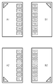
도 3은 본 발명의 바람직한 실시예에 따른 반도체 메모리 모듈에서 터미널의 배치를 나타내는 도면이다.3 is a diagram illustrating an arrangement of terminals in a semiconductor memory module according to an exemplary embodiment of the present invention.
도 3에는 다수의 터미널들(CA1~CA4, DQ1~DQ4)을 각각 구비하는 다수의 반도체 메모리 소자들(A1,B1, A2, B2), 다수의 트레이스들(trace10, trace21, trace22) 및 다수의 스터브들(stub31, stub32, stub33, stub34)이 도시되어 있다. 3 illustrates a plurality of semiconductor memory devices A1, B1, A2, and B2, a plurality of traces trace10, trace21, and trace22, and a plurality of terminals each having a plurality of terminals CA1 to CA4 and DQ1 to DQ4. Stubs (stub31, stub32, stub33, stub34) are shown.
도 3에 도시된 반도체 메모리 모듈은 2 열[제 1 열의 제 1 반도체 메모리 소자들 (A1, A2) 및 제 2 열의 제 2 반도체 메모리 소자들(B1, B2)]의 반도체 메모리 소자들을 구비하고 있다. 본 발명에 따른 반도체 메모리 모듈은 2 열 이상의 반도체 메모리 소자들을 구비하며, 이와 같이 2 열의 이상의 반도체 메모리 소자들을 반도체 메모리 모듈에 구비시킴으로써 고집적(high density)의 반도체 메모리 모듈을 구현할 수 있다.The semiconductor memory module shown in FIG. 3 includes semiconductor memory elements in two rows (first semiconductor memory elements A1 and A2 in the first row and second semiconductor memory elements B1 and B2 in the second row). . The semiconductor memory module according to the present invention includes two or more rows of semiconductor memory devices, and thus, by providing two or more rows of semiconductor memory devices in the semiconductor memory module, a high density semiconductor memory module can be realized.
도 3과 도 2를 비교하면 알 수 있듯이, 본 발명에 따른 반도체 메모리 모듈에서는 소정의 터미널들(CA1~CA4)이 에지 영역(edge region)에 배치된다. 즉, 제 1 반도체 메모리 소자 A1의 터미널들 중에서 소정의 터미널들(CA1~CA4)은 제 1 반도체 메모리 소자 A1의 에지 영역들(예컨대, 상하좌우의 에지 영역들) 중에서 제 2 반도체 메모리 소자 B1에 근접한 에지 영역에 배치되고, 제 2 반도체 메모리 소자 B1의 소정 터미널들(CA1~CA4)은 제 2 반도체 메모리 소자 B1의 에지 영역들(예컨대, 상하좌우의 에지 영역들) 중에서 제 1 반도체 메모리 소자 A1에 근접한 에지 영역에 배치된다. 그리고, 제 1 반도체 메모리 소자 A1의 소정 터미널들(CA1~CA4)과 제 2 반도체 메모리 소자 B1의 소정 터미널들(CA1~CA4)은 서로 대칭이 되도록 배치된다. 도 3에서 보듯이, 제 1 반도체 메모리 소자 A2 및 제 2 반도체 메모리 소자 B2의 경우에서도 마찬가지로, 소정 터미널들 CA1~CA4은 각각의 에지 영역에 대칭적으로 배치된다. 한편, 도 3에서는 소정 터미널들 CA1~CA4 뿐만 아니라 터미널들 DQ1~DQ4도 각각의 에지 영역에 대칭적으로 배치되어 있다.As can be seen by comparing FIG. 3 with FIG. 2, in the semiconductor memory module according to the present invention, predetermined terminals CA1 to CA4 are disposed in an edge region. That is, predetermined terminals CA1 to CA4 among the terminals of the first semiconductor memory device A1 may be connected to the second semiconductor memory device B1 among the edge regions (eg, top, bottom, left and right edge regions) of the first semiconductor memory element A1. Predetermined terminals CA1 to CA4 of the second semiconductor memory device B1 are disposed in an adjacent edge area, and the first semiconductor memory device A1 is disposed among the edge areas of the second semiconductor memory device B1 (eg, top, bottom, left and right edge areas). It is placed in the edge region close to. The predetermined terminals CA1 to CA4 of the first semiconductor memory device A1 and the predetermined terminals CA1 to CA4 of the second semiconductor memory device B1 are arranged to be symmetrical with each other. As shown in Fig. 3, in the case of the first semiconductor memory element A2 and the second semiconductor memory element B2, similarly, the predetermined terminals CA1 to CA4 are symmetrically arranged in the respective edge regions. Meanwhile, in FIG. 3, terminals DQ1 to DQ4 as well as predetermined terminals CA1 to CA4 are symmetrically disposed in each edge region.
제 1 반도체 메모리 소자 A1의 터미널 CA1, 제 2 반도체 메모리 소자 B1의 터미널 CA1, 제 3 반도체 메모리 소자 A2의 터미널 CA1 및 제 4 반도체 메모리 소자 B2의 터미널 CA1은 멀티 드롭(Multi-drop) 방식에 의하여 서로 연결된다. 제 1 반도체 메모리 소자 A1의 터미널 CA1과 제 2 반도체 메모리 소자 B1의 터미널 CA1은 trace21으로부터 신호를 공통적으로 입력받으며, 제 3 반도체 메모리 소자 A2의 터미널 CA1과 제 4 반도체 메모리 소자 B2의 터미널 CA1은 trace22로부터 신호를 공통적으로 입력받는다. 제 1 반도체 메모리 소자 A1의 터미널 CA1, 제 2 반도체 메모리 소자 B1의 터미널 CA1, 제 3 반도체 메모리 소자 A2의 터미널 CA1 및 제 4 반도체 메모리 소자 B2의 터미널 CA1은 trace10으로부터 신호를 공통적으로 입력받는 공통(common) 관계의 터미널들이다. 비록 도 3에 직접적으로 도시되어 있지는 않지만, 이와 같은 멀티 드롭(multi-drop) 방식은 터미널 CA2, 터미널 CA3 및 터미널 CA4에도 동일하게 적용된다. 한편, 개별적으로 데이터 신호(data signal)를 입 력받거나 출력하는 터미널들 DQ1~DQ4는 공통(common) 관계의 터미널들에 해당되지 않는다. The terminal CA1 of the first semiconductor memory element A1, the terminal CA1 of the second semiconductor memory element B1, the terminal CA1 of the third semiconductor memory element A2, and the terminal CA1 of the fourth semiconductor memory element B2 are connected by a multi-drop method. Are connected to each other. Terminal CA1 of the first semiconductor memory device A1 and terminal CA1 of the second semiconductor memory device B1 receive signals from trace21 in common, and terminal CA1 of the third semiconductor memory device A2 and terminal CA1 of the fourth semiconductor memory device B2 are trace22. Receive a common signal from. The terminal CA1 of the first semiconductor memory element A1, the terminal CA1 of the second semiconductor memory element B1, the terminal CA1 of the third semiconductor memory element A2, and the terminal CA1 of the fourth semiconductor memory element B2 are commonly received signals from trace10 in common ( common) terminals of a relationship. Although not shown directly in FIG. 3, this multi-drop scheme applies equally to terminal CA2, terminal CA3 and terminal CA4. Meanwhile, terminals DQ1 to DQ4 that individually receive or output data signals do not correspond to terminals having a common relationship.
도 3에서는, 전원 신호(power/ground signal)에 관계되는 터미널들이나 클럭 신호(clock signal)에 관계되는 터미널들 등은 생략되고, 데이터 신호(data signal)에 관계되는 터미널들(DQ1~DQ4)과 커맨드 신호(command signal) 또는 어드레스 신호(address signal)에 관계되는 터미널들(CA1~CA4)이 대표적으로 도시되어 있다.In FIG. 3, terminals related to a power / ground signal, terminals related to a clock signal, and the like are omitted, and terminals DQ1 to DQ4 related to a data signal are omitted. Terminals CA1 to CA4 related to the command signal or address signal are representatively shown.
도 3의 경우도 도 2의 경우와 마찬가지로, 데이터 신호를 입력받거나 출력하는 터미널들 DQ1~DQ4는 개별적으로 신호를 입력받거나 출력하고, 커맨드 신호 또는 어드레스 신호를 입력받는 터미널들 CA1~CA4의 경우에 공통(common) 관계의 터미널들은 공통의 트레이스로부터 커맨드 신호 또는 어드레스 신호를 공통적으로 입력받는다. 다만, 커맨드 신호와 어드레스 신호는 대표적인 예시에 불과하며, 본 발명의 실시예가 커맨드 신호 또는 어드레스 신호를 입력받는 경우만으로 한정되는 것은 아니다. 즉, 상기 공통(common) 관계의 터미널들은 공통의 트레이스로부터 멀티 드롭(multi-drop) 방식으로 입력되는 신호를 공통적으로 입력받는다고 할 수 있다.3, as in the case of FIG. 2, the terminals DQ1 to DQ4 that receive or output data signals are individually input or output signals, and terminals CA1 to CA4 that receive command signals or address signals. Terminals having a common relationship commonly receive a command signal or an address signal from a common trace. However, the command signal and the address signal are merely representative examples, and embodiments of the present invention are not limited to the case where the command signal or the address signal is input. That is, the terminals of the common relationship may be said to receive a signal input in a multi-drop manner from a common trace in common.
제 1 반도체 메모리 소자 A1의 터미널 CA1은 stub31, 공통의 트레이스(trace21, trace10) 및 공통의 모듈 탭(TAB)을 통하여 외부의 메모리 컨트롤러(예컨대, 도 1b에서의 120)로부터 신호를 입력받고, 제 2 반도체 메모리 소자 B1의 터미널 CA1은 stub32, 공통의 트레이스(trace21, trace10) 및 공통의 모듈 탭(TAB)을 통하여 외부의 메모리 컨트롤러로부터 신호를 입력받는다. 제 1 반도체 메모리 소자 A1의 터미널 CA1과 제 2 반도체 메모리 소자 B1의 터미널 CA1을 서로 근접한 에지 영역들에 대칭적으로 각각 배치시킴으로써, stub31의 길이 및 stub32의 길이를 최소화할 수 있다.The terminal CA1 of the first semiconductor memory device A1 receives a signal from an external memory controller (eg, 120 in FIG. 1B) through a stub31,
그리고, 제 3 반도체 메모리 소자 A2의 터미널 CA1은 stub33, 공통의 트레이스(trace22, trace10) 및 공통의 모듈 탭(TAB)을 통하여 외부의 메모리 컨트롤러로부터 신호를 입력받고, 제 4 반도체 메모리 소자 B2의 터미널 CA1은 stub34, 공통의 트레이스(trace22, trace10) 및 공통의 모듈 탭(TAB)을 통하여 외부의 메모리 컨트롤러로부터 신호를 입력받는다. 제 3 반도체 메모리 소자 A2의 터미널 CA1과 제 4 반도체 메모리 소자 B2의 터미널 CA1을 서로 근접한 에지 영역들에 대칭적으로 각각 배치시킴으로써, stub33의 길이 및 stub34의 길이를 최소화할 수 있다.The terminal CA1 of the third semiconductor memory device A2 receives a signal from an external memory controller through the stub33, the common traces trace22 and trace10, and the common module tap TAB, and the terminal of the fourth semiconductor memory device B2. CA1 receives signals from an external memory controller through stub34, common traces trace22 and trace10, and common module tap TAB. By symmetrically disposing the terminal CA1 of the third semiconductor memory element A2 and the terminal CA1 of the fourth semiconductor memory element B2 in the edge regions adjacent to each other, the length of the stub33 and the length of the stub34 can be minimized.
이와 같이 본 발명에 따른 반도체 메모리 모듈에서는, 공통(common) 관계의 터미널들을 서로 근접한 에지 영역들에 대칭적으로 각각 배치시킴으로써, 각각의 스터브의 길이를 최소화(예컨대, stub31의 길이 및 stub32의 길이를 최소화하고 stub33의 길이 및 stub34의 길이를 최소화)한다. 각각의 스터브의 길이(stub length)를 최소화하면 반도체 메모리 모듈의 동작을 상대적으로 더 고속화시킬 수 있다. As described above, in the semiconductor memory module according to the present invention, the terminals of common relations are symmetrically disposed in adjacent edge regions, thereby minimizing the length of each stub (eg, the length of stub31 and the length of stub32). Minimize the length of stub33 and the length of stub34). Minimizing the stub length of each stub may relatively speed up the operation of the semiconductor memory module.
도 3에서 제 1 반도체 메모리 소자 A1의 소정 터미널들(CA1~CA4), 제 2 반도체 메모리 소자 B1의 소정 터미널들(CA1~CA4), 제 3 반도체 메모리 소자 A2의 소정 터미널들(CA1~CA4) 및 제 4 반도체 메모리 소자 B2의 소정 터미널들(CA1~CA4)은 본딩 패드(bonding pad)들, 솔더 볼 패드(solder ball pad)들, 재배선(RDL: ReDistribution Line) 패드들 또는 플립칩 범핑 패드(flip-chip bumping pad)들 등을 나타낸다고 할 수 있다. 다만, 본 발명의 실시예가 위와 같은 패드들의 경우만으로 한정되는 것은 아니며, 상호 접속 터미널(interconnection terminal)으로서의 다양한 패드들을 배치함에 있어서 본 발명이 적용될 수 있다.3, predetermined terminals CA1 to CA4 of the first semiconductor memory device A1, predetermined terminals CA1 to CA4 of the second semiconductor memory device B1, and predetermined terminals CA1 to CA4 of the third semiconductor memory device A2. The predetermined terminals CA1 to CA4 of the fourth semiconductor memory device B2 may include bonding pads, solder ball pads, redistribution line pads, or flip chip bumping pads. (flip-chip bumping pads) and the like. However, the embodiment of the present invention is not limited to the case of the above pads, and the present invention can be applied in arranging various pads as interconnect terminals.
도 3에서 제 1 반도체 메모리 소자 A1 및 제 4 반도체 메모리 소자 B2는 M 타입으로 도시되어 있고, 제 2 반도체 메모리 소자 B1 및 제 3 반도체 메모리 소자 A2는 N 타입으로 도시되어 있다. 도 4a를 참조하여 M 타입과 N 타입을 설명한다.In FIG. 3, the first semiconductor memory element A1 and the fourth semiconductor memory element B2 are shown as M type, and the second semiconductor memory element B1 and the third semiconductor memory element A2 are shown as N type. The M type and the N type will be described with reference to FIG. 4A.
도 4a 및 도 4b는 본 발명에 따른 반도체 메모리 모듈의 다양한 실시예를 설명하기 위한 도면이다.4A and 4B illustrate various embodiments of a semiconductor memory module according to the present invention.
도 4a에서 보듯이, 제 1 반도체 메모리 소자 A1의 터미널들 중에서 소정의 터미널들(TA1~TA7)과 제 2 반도체 메모리 소자 B1의 소정 터미널들(TB1~TB7)은 서로 거울 대칭의 형태가 되도록 배치되고, 제 3 반도체 메모리 소자 A2의 소정 터미널들(TC7~TC1)과 제 4 반도체 메모리 소자 B2의 소정 터미널들(TD7~TD1)은 서로 거울 대칭의 형태가 되도록 배치된다. 제 1 형태(M 타입)와 제 2 형태(N 타입)가 쌍을 이루어 상기 거울 대칭의 형태를 구성하는 경우에, 제 1 반도체 메모리 소자 A1의 소정 터미널들(TA1~TA7)은 제 1 형태(M 타입)가 되도록 형성되고, 제 2 반도체 메모리 소자 B1의 소정 터미널들(TB1~TB7)은 제 2 형태(N 타입)가 되도록 형성된다. 또한, 제 3 반도체 메모리 소자 A2의 소정 터미널들(TC7~TC1)은 제 2 형태(N 타입)가 되도록 형성되고, 제 4 반도체 메모리 소자 B2의 소정 터미널들(TD7~TD1)은 제 1 형태(M 타입)가 되도록 형성된다. As shown in FIG. 4A, among terminals of the first semiconductor memory device A1, predetermined terminals TA1 to TA7 and predetermined terminals TB1 to TB7 of the second semiconductor memory device B1 are arranged to be mirror symmetric with each other. The predetermined terminals TC7 to TC1 of the third semiconductor memory device A2 and the predetermined terminals TD7 to TD1 of the fourth semiconductor memory device B2 are arranged to be mirror symmetric with each other. When the first form (type M) and the second form (type N) form a pair to form the mirror symmetrical form, the predetermined terminals TA1 to TA7 of the first semiconductor memory device A1 are configured as the first form ( M type) and predetermined terminals TB1 to TB7 of the second semiconductor memory device B1 are formed to have a second shape (N type). In addition, the predetermined terminals TC7 to TC1 of the third semiconductor memory device A2 are formed to be of the second type (N type), and the predetermined terminals TD7 to TD1 of the fourth semiconductor memory device B2 are of the first type ( M type).
이와 같이, 쌍을 이루는 반도체 메모리 소자들(A1과 B1, A2와 B2)의 소정 터미널들이 서로 거울 대칭의 형태가 되도록 배치되려면, 쌍을 이루는 반도체 메모리 소자들(A1과 B1, A2와 B2) 중에서 어느 하나의 반도체 메모리 소자의 소정 터미널들은 제 1 형태(M 타입)가 되도록 형성되어야 하고, 쌍을 이루는 반도체 메모리 소자들(A1과 B1, A2와 B2) 중에서 다른 하나의 반도체 메모리 소자의 소정 터미널들은 제 2 형태(N 타입)가 되도록 형성되어야 한다. 거울 대칭의 형태를 위한 반도체 메모리 소자의 2 가지 제작 방식을 다음과 같이 고려해 볼 수 있다. As such, if the predetermined terminals of the paired semiconductor memory elements A1 and B1, A2 and B2 are arranged to be mirror symmetrical with each other, among the paired semiconductor memory elements A1 and B1, A2 and B2. Predetermined terminals of one of the semiconductor memory devices must be formed to have a first type (M type), and predetermined terminals of the other semiconductor memory device among the paired semiconductor memory devices A1 and B1, A2 and B2 It should be formed to have a second form (N type). Two fabrication methods of a semiconductor memory device for the form of mirror symmetry can be considered as follows.
첫번째 제작 방식은 처음부터 반도체 메모리 소자들을 M 타입과 N 타입으로 분류해서 별도로 제작하는 방식이다. 첫번째 제작 방식에 의하면, 도 4a에서, 제 1 반도체 메모리 소자 A1의 소정 터미널들(TA1~TA7) 및 제 4 반도체 메모리 소자 B2의 소정 터미널들(TD7~TD1)은 처음부터 제 1 형태(M 타입)가 되도록 형성된다. 이와 별도로, 제 2 반도체 메모리 소자 B1의 소정 터미널들(TB1~TB7) 및 제 3 반도체 메모리 소자 A2의 소정 터미널들(TC7~TC1)은 처음부터 제 2 형태(N 타입)가 되도록 형성된다.In the first manufacturing method, semiconductor memory devices are classified into M type and N type and manufactured separately from the beginning. According to the first fabrication method, in FIG. 4A, predetermined terminals TA1 to TA7 of the first semiconductor memory device A1 and predetermined terminals TD7 to TD1 of the fourth semiconductor memory device B2 may be configured from the first type (M type). It is formed to be. Separately, the predetermined terminals TB1 to TB7 of the second semiconductor memory device B1 and the predetermined terminals TC7 to TC1 of the third semiconductor memory device A2 are formed to have a second shape (N type) from the beginning.
두번째 제작 방식은, 1 차적으로 반도체 메모리 소자들을 모두 기본 형태로 제작한 후에, 2 차적으로 스위칭 옵션(switching option) 또는 퓨즈 커팅(fuse cutting)에 의해서 어떤 반도체 메모리 소자들은 M 타입이 되도록 하고 다른 반도체 메모리 소자들은 N 타입이 되도록 하는 방식이다. 두번째 제작 방식에 의하면, 도 4a에서, 1 차적으로 제 1 반도체 메모리 소자 A1, 제 2 반도체 메모리 소자 B1, 제 3 반도체 메모리 소자 A2 및 제 4 반도체 메모리 소자 B2는 모두 기본 형태로 제작되고, 2 차적으로 스위칭 옵션이나 퓨즈 커팅에 의해서, 제 1 반도체 메모리 소자 A1의 소정 터미널들(TA1~TA7) 및 제 4 반도체 메모리 소자 B2의 소정 터미널들(TD7~TD1)은 제 1 형태(M 타입)로 되고, 제 2 반도체 메모리 소자 B1의 소정 터미널들(TB1~TB7) 및 제 3 반도체 메모리 소자 A2의 소정 터미널들(TC7~TC1)은 제 2 형태(N 타입)로 된다.In the second fabrication method, after fabricating all semiconductor memory devices in a basic form, some semiconductor memory devices are made to be M type by switching or fuse cutting. The memory elements are N type. According to the second fabrication method, in FIG. 4A, the first semiconductor memory device A1, the second semiconductor memory device B1, the third semiconductor memory device A2, and the fourth semiconductor memory device B2 are all manufactured in a basic form. By the switching option or the fuse cutting, the predetermined terminals TA1 to TA7 of the first semiconductor memory element A1 and the predetermined terminals TD7 to TD1 of the fourth semiconductor memory element B2 are of the first type (type M). The predetermined terminals TB1 to TB7 of the second semiconductor memory device B1 and the predetermined terminals TC7 to TC1 of the third semiconductor memory device A2 have a second type (N type).
한편, 도 3 및 도 4a에서 살펴본 제 1 반도체 메모리 소자 A1, 제 2 반도체 메모리 소자 B1, 제 3 반도체 메모리 소자 A2 및 제 4 반도체 메모리 소자 B2는 칩(chip), 재배선(RDL:ReDistribution Line) 칩, 패키지(package) 또는 웨이퍼 레벨 패키지(wafer level package) 등을 나타낸다고 할 수 있다. 그리고, 도 3 및 도 4a에서 살펴본 반도체 메모리 소자의 범위에는 단일 소자(mono device) 또는 단일 소자들이 적층된 적층 소자(stack device) 등이 포함된다. 특히, 도 4b에는 단일 칩들(chip1, chip2)이 적층된 반도체 메모리 소자가 예시되어 있다. 다만, 본 발명의 실시예가 앞서 예시한 반도체 메모리 소자들의 경우만으로 한정되는 것은 아니며, 본 발명은 그 외에도 다양한 반도체 메모리 소자들을 구비하는 반도체 메모리 모듈에 적용될 수 있다.Meanwhile, the first semiconductor memory device A1, the second semiconductor memory device B1, the third semiconductor memory device A2, and the fourth semiconductor memory device B2 described with reference to FIGS. 3 and 4A may have a chip and a redistribution line (RDL). It can be said that it represents a chip, a package or a wafer level package. In addition, the range of the semiconductor memory device described with reference to FIGS. 3 and 4A includes a mono device or a stack device in which single devices are stacked. In particular, FIG. 4B illustrates a semiconductor memory device in which single chips chip1 and chip2 are stacked. However, embodiments of the present invention are not limited to the above-described semiconductor memory devices, and the present invention may be applied to a semiconductor memory module including various semiconductor memory devices.
이상에서는 본 발명을 장치 발명의 측면에서 설명하였으나, 본 발명은 다음과 같이 방법 발명의 측면에서 파악될 수도 있다. 즉, 제 1 반도체 메모리 소자(A1) 내지 제 4 반도체 메모리 소자(B2)를 구비하는 반도체 메모리 모듈에서의 터미널 배치 방법에 있어서, 본 발명에 따른 반도체 메모리 모듈에서의 터미널 배치 방법을 다음과 같은 기술적 특징을 구비한다. 이하에서는 도 3을 참조하여 설명 한다.The present invention has been described above in terms of device invention, but the present invention may be understood in terms of method invention as follows. That is, in the method for arranging terminals in a semiconductor memory module including the first semiconductor memory elements A1 to the fourth semiconductor memory element B2, the terminal arranging method in the semiconductor memory module according to the present invention is described as follows. Features. A description with reference to FIG. 3 is as follows.
제 1 반도체 메모리 소자(A1)의 소정 터미널들(CA1~CA4)은 제 2 반도체 메모리 소자(B1)에 근접한 에지 영역에 배치하고, 제 2 반도체 메모리 소자(B1)의 소정 터미널들(CA1~CA4)은 제 1 반도체 메모리 소자(A1)에 근접한 에지 영역에 배치하되, 제 1 반도체 메모리 소자(A1)의 소정 터미널들(CA1~CA4)과 제 2 반도체 메모리 소자(B1)의 소정 터미널들(CA1~CA4)은 서로 대칭이 되도록 배치한다. 그리고, 제 3 반도체 메모리 소자(A2)의 소정 터미널들(CA1~CA4)은 제 4 반도체 메모리 소자(B2)에 근접한 에지 영역에 배치하고, 제 4 반도체 메모리 소자(B2)의 소정 터미널들(CA1~CA4)은 제 3 반도체 메모리 소자(A2)에 근접한 에지 영역에 배치하되, 제 3 반도체 메모리 소자(A2)의 소정 터미널들(CA1~CA4)과 제 4 반도체 메모리 소자(B2)의 소정 터미널들(CA1~CA4)은 서로 대칭이 되도록 배치한다.Predetermined terminals CA1 to CA4 of the first semiconductor memory device A1 are disposed in an edge region proximate the second semiconductor memory device B1, and predetermined terminals CA1 to CA4 of the second semiconductor memory device B1. ) Is disposed in an edge region proximate the first semiconductor memory device A1, and predetermined terminals CA1 to CA4 of the first semiconductor memory device A1 and predetermined terminals CA1 of the second semiconductor memory device B1. ~ CA4) is arranged to be symmetrical to each other. Predetermined terminals CA1 to CA4 of the third semiconductor memory device A2 are disposed in an edge region proximate the fourth semiconductor memory device B2, and predetermined terminals CA1 of the fourth semiconductor memory device B2. CA4 may be disposed in an edge region proximate the third semiconductor memory device A2, and predetermined terminals CA1 to CA4 of the third semiconductor memory device A2 and predetermined terminals of the fourth semiconductor memory device B2. CA1 to CA4 are arranged to be symmetrical with each other.
도 3에서 보듯이, 제 1 반도체 메모리 소자(A1) 내지 제 4 반도체 메모리 소자(B2) 각각이 터미널 1 내지 터미널 N을 구비하는 경우에, 제 1 반도체 메모리 소자(A1)의 터미널 n(예컨대, CA1), 제 2 반도체 메모리 소자(B1)의 터미널 n(예컨대, CA1), 제 3 반도체 메모리 소자(A2)의 터미널 n(예컨대, CA1) 및 제 4 반도체 메모리 소자(B2)의 터미널 n(예컨대, CA1)은, 공통의 트레이스(trace10)로부터 커맨드 신호 또는 어드레스 신호를 공통적으로 입력받는 공통 관계의 터미널들이다. 여기서, n은 1~N 중에서 임의의 자연수를 나타낸다.As shown in FIG. 3, when each of the first to fourth semiconductor memory elements A1 to B2 includes
제 1 반도체 메모리 소자(A1)의 터미널 n(예컨대, CA1)은 제 1 스터브(예컨대, stub31), 공통의 트레이스(trace21, trace10) 및 공통의 모듈 탭(TAB)을 통하 여 외부의 메모리 컨트롤러(예컨대, 도 1b에서의 120)로부터 신호를 입력받는다. 제 2 반도체 메모리 소자(B1)의 터미널 n(예컨대, CA1)은 제 2 스터브(예컨대, stub32), 공통의 트레이스(trace21, trace10) 및 공통의 모듈 탭(TAB)을 통하여 외부의 메모리 컨트롤러로부터 신호를 입력받는다. 제 3 반도체 메모리 소자(A2)의 터미널 n(예컨대, CA1)은 제 3 스터브(예컨대, stub33), 공통의 트레이스(trace22, trace10) 및 공통의 모듈 탭(TAB)을 통하여 외부의 메모리 컨트롤러로부터 신호를 입력받는다. 제 4 반도체 메모리 소자(B2)의 터미널 n(예컨대, CA1)은 제 4 스터브(예컨대, stub34), 공통의 트레이스(trace22, trace10) 및 공통의 모듈 탭(TAB)을 통하여 외부의 메모리 컨트롤러로부터 신호를 입력받는다. Terminal n (eg, CA1) of the first semiconductor memory device A1 may be connected to an external memory controller (eg, through a first stub (eg, stub31),
이와 같은 경우에, 제 1 반도체 메모리 소자(A1)의 터미널 n(예컨대, CA1)과 제 2 반도체 메모리 소자(B1)의 터미널 n(예컨대, CA1)을 서로 근접한 에지 영역들에 대칭적으로 각각 배치하고, 제 3 반도체 메모리 소자(A2)의 터미널 n(예컨대, CA1)과 제 4 반도체 메모리 소자(B2)의 터미널 n(예컨대, CA1)을 서로 근접한 에지 영역들에 대칭적으로 각각 배치함으로써, 제 1 스터브(예컨대, stub31)의 길이, 제 2 스터브(예컨대, stub32)의 길이, 제 3 스터브(예컨대, stub33)의 길이 및 제 4 스터브(예컨대, stub34)의 길이를 최소화할 수 있다.In such a case, the terminal n of the first semiconductor memory element A1 (eg, CA1) and the terminal n of the second semiconductor memory element B1 (eg, CA1) are symmetrically arranged in adjacent edge regions, respectively. The terminal n (eg, CA1) of the third semiconductor memory device A2 and the terminal n (eg, CA1) of the fourth semiconductor memory device B2 are symmetrically disposed in edge regions proximate to each other, respectively. The length of one stub (eg stub31), the length of the second stub (eg stub32), the length of the third stub (eg stub33) and the length of the fourth stub (eg stub34) can be minimized.
이상에서는 도면에 도시된 구체적인 실시예를 참고하여 본 발명을 설명하였으나 이는 예시적인 것에 불과하므로, 본 발명이 속하는 기술 분야에서 통상의 기술을 가진 자라면 이로부터 다양한 수정 및 변형이 가능할 것이다. 따라서, 본 발명의 보호 범위는 후술하는 특허청구범위에 의하여 해석되어야 하고, 그와 동등 및 균등한 범위 내에 있는 모든 기술적 사상은 본 발명의 보호 범위에 포함되는 것으로 해석되어야 할 것이다.In the above described the present invention with reference to the specific embodiment shown in the drawings, but this is only an example, those of ordinary skill in the art to which the present invention pertains various modifications and variations therefrom. Therefore, the protection scope of the present invention should be interpreted by the claims to be described later, and all the technical ideas within the equivalent and equivalent ranges should be construed as being included in the protection scope of the present invention.
본 발명에 따른 반도체 메모리 모듈에서는 공통(common) 관계의 터미널들이 서로 근접한 에지 영역들에 대칭적으로 각각 배치됨으로써 각각의 스터브의 길이(stub length)가 최소화되므로, 본 발명에 의하면 반도체 메모리 모듈의 동작을 상대적으로 더 고속화시킬 수 있다. In the semiconductor memory module according to the present invention, since the terminals of common relation are symmetrically arranged in adjacent edge regions, the stub length of each stub is minimized. Can be made relatively faster.
Claims (20)
Priority Applications (2)
| Application Number | Priority Date | Filing Date | Title |
|---|---|---|---|
| KR1020060115421A KR100791003B1 (en) | 2006-11-21 | 2006-11-21 | Terminal arrangement method in semiconductor memory module and semiconductor memory module |
| US11/980,347 US20080116572A1 (en) | 2006-11-21 | 2007-10-31 | Semiconductor memory modules, methods of arranging terminals therein, and methods of using thereof |
Applications Claiming Priority (1)
| Application Number | Priority Date | Filing Date | Title |
|---|---|---|---|
| KR1020060115421A KR100791003B1 (en) | 2006-11-21 | 2006-11-21 | Terminal arrangement method in semiconductor memory module and semiconductor memory module |
Publications (1)
| Publication Number | Publication Date |
|---|---|
| KR100791003B1 true KR100791003B1 (en) | 2008-01-03 |
Family
ID=39216455
Family Applications (1)
| Application Number | Title | Priority Date | Filing Date |
|---|---|---|---|
| KR1020060115421A Expired - Fee Related KR100791003B1 (en) | 2006-11-21 | 2006-11-21 | Terminal arrangement method in semiconductor memory module and semiconductor memory module |
Country Status (2)
| Country | Link |
|---|---|
| US (1) | US20080116572A1 (en) |
| KR (1) | KR100791003B1 (en) |
Families Citing this family (4)
| Publication number | Priority date | Publication date | Assignee | Title |
|---|---|---|---|---|
| JP6543129B2 (en) * | 2015-07-29 | 2019-07-10 | ルネサスエレクトロニクス株式会社 | Electronic device |
| KR20180090494A (en) | 2017-02-03 | 2018-08-13 | 삼성전자주식회사 | Method for fabricating substrate structure |
| KR102781129B1 (en) | 2020-08-06 | 2025-03-12 | 삼성전자주식회사 | Semiconductor chip module |
| JP2023045844A (en) * | 2021-09-22 | 2023-04-03 | キオクシア株式会社 | Semiconductor device and memory system |
Citations (4)
| Publication number | Priority date | Publication date | Assignee | Title |
|---|---|---|---|---|
| JPH06350052A (en) * | 1993-06-11 | 1994-12-22 | Hitachi Ltd | Semiconductor memory device |
| JPH0786526A (en) * | 1993-09-14 | 1995-03-31 | Toshiba Corp | Memory device |
| JP2000021177A (en) | 1998-06-30 | 2000-01-21 | Fujitsu Ltd | Semiconductor storage device |
| JP2005328069A (en) | 2000-09-08 | 2005-11-24 | Seiko Epson Corp | Semiconductor chip and semiconductor device |
Family Cites Families (5)
| Publication number | Priority date | Publication date | Assignee | Title |
|---|---|---|---|---|
| US5955889A (en) * | 1994-05-20 | 1999-09-21 | Fujitsu Limited | Electronic circuit apparatus for transmitting signals through a bus and semiconductor device for generating a predetermined stable voltage |
| JP3768761B2 (en) * | 2000-01-31 | 2006-04-19 | 株式会社日立製作所 | Semiconductor device and manufacturing method thereof |
| US6731011B2 (en) * | 2002-02-19 | 2004-05-04 | Matrix Semiconductor, Inc. | Memory module having interconnected and stacked integrated circuits |
| US6597062B1 (en) * | 2002-08-05 | 2003-07-22 | High Connection Density, Inc. | Short channel, memory module with stacked printed circuit boards |
| US6876562B2 (en) * | 2002-10-17 | 2005-04-05 | Micron Technology, Inc. | Apparatus and method for mounting microelectronic devices on a mirrored board assembly |
-
2006
- 2006-11-21 KR KR1020060115421A patent/KR100791003B1/en not_active Expired - Fee Related
-
2007
- 2007-10-31 US US11/980,347 patent/US20080116572A1/en not_active Abandoned
Patent Citations (4)
| Publication number | Priority date | Publication date | Assignee | Title |
|---|---|---|---|---|
| JPH06350052A (en) * | 1993-06-11 | 1994-12-22 | Hitachi Ltd | Semiconductor memory device |
| JPH0786526A (en) * | 1993-09-14 | 1995-03-31 | Toshiba Corp | Memory device |
| JP2000021177A (en) | 1998-06-30 | 2000-01-21 | Fujitsu Ltd | Semiconductor storage device |
| JP2005328069A (en) | 2000-09-08 | 2005-11-24 | Seiko Epson Corp | Semiconductor chip and semiconductor device |
Also Published As
| Publication number | Publication date |
|---|---|
| US20080116572A1 (en) | 2008-05-22 |
Similar Documents
| Publication | Publication Date | Title |
|---|---|---|
| KR101924388B1 (en) | Semiconductor Package having a redistribution structure | |
| US7675181B2 (en) | Planar multi semiconductor chip package and method of manufacturing the same | |
| US20100270668A1 (en) | Dual Interconnection in Stacked Memory and Controller Module | |
| US20020088633A1 (en) | Multi-chip memory devices, modules and control methods including independent control of memory chips | |
| US9559079B2 (en) | Semiconductor stack packages | |
| US8319324B2 (en) | High I/O semiconductor chip package and method of manufacturing the same | |
| CN106057748B (en) | Semiconductor package | |
| TW201618238A (en) | Die stacking technology in BGA memory package for small footprint CPU and memory motherboard design | |
| US10679956B2 (en) | Semiconductor memory chip, semiconductor memory package, and electronic system using the same | |
| KR20210077290A (en) | Semiconductor package including stacked semiconductor chips | |
| US9219050B2 (en) | Microelectronic unit and package with positional reversal | |
| US8283765B2 (en) | Semiconductor chip and stacked semiconductor package having the same | |
| KR20180067695A (en) | High Bandwidth Memory Applications with Controlled Impedance Load | |
| US20160056130A1 (en) | Semiconductor integrated circuit including power tsvs | |
| US20160093599A1 (en) | Semiconductor device | |
| KR100791003B1 (en) | Terminal arrangement method in semiconductor memory module and semiconductor memory module | |
| JP4754201B2 (en) | Semiconductor device | |
| KR100359591B1 (en) | Semiconductor device | |
| US9226398B1 (en) | Printed circuit board and package substrate having additional conductive pathway space | |
| KR20050023167A (en) | Structure of a Memory module | |
| KR20050048900A (en) | Memory module having the mirror type package of semiconductor memory chips | |
| KR100671950B1 (en) | Stack package | |
| KR20050099158A (en) | Memory module having mirror package | |
| KR20090084185A (en) | Stacked Wafer Level Semiconductor Packages |
Legal Events
| Date | Code | Title | Description |
|---|---|---|---|
| A201 | Request for examination | ||
| PA0109 | Patent application |
St.27 status event code: A-0-1-A10-A12-nap-PA0109 |
|
| PA0201 | Request for examination |
St.27 status event code: A-1-2-D10-D11-exm-PA0201 |
|
| D13-X000 | Search requested |
St.27 status event code: A-1-2-D10-D13-srh-X000 |
|
| D14-X000 | Search report completed |
St.27 status event code: A-1-2-D10-D14-srh-X000 |
|
| E701 | Decision to grant or registration of patent right | ||
| PE0701 | Decision of registration |
St.27 status event code: A-1-2-D10-D22-exm-PE0701 |
|
| GRNT | Written decision to grant | ||
| PR0701 | Registration of establishment |
St.27 status event code: A-2-4-F10-F11-exm-PR0701 |
|
| PR1002 | Payment of registration fee |
St.27 status event code: A-2-2-U10-U11-oth-PR1002 Fee payment year number: 1 |
|
| PG1601 | Publication of registration |
St.27 status event code: A-4-4-Q10-Q13-nap-PG1601 |
|
| PR1001 | Payment of annual fee |
St.27 status event code: A-4-4-U10-U11-oth-PR1001 Fee payment year number: 4 |
|
| PR1001 | Payment of annual fee |
St.27 status event code: A-4-4-U10-U11-oth-PR1001 Fee payment year number: 5 |
|
| R18-X000 | Changes to party contact information recorded |
St.27 status event code: A-5-5-R10-R18-oth-X000 |
|
| FPAY | Annual fee payment |
Payment date: 20121130 Year of fee payment: 6 |
|
| PR1001 | Payment of annual fee |
St.27 status event code: A-4-4-U10-U11-oth-PR1001 Fee payment year number: 6 |
|
| FPAY | Annual fee payment |
Payment date: 20131129 Year of fee payment: 7 |
|
| PR1001 | Payment of annual fee |
St.27 status event code: A-4-4-U10-U11-oth-PR1001 Fee payment year number: 7 |
|
| LAPS | Lapse due to unpaid annual fee | ||
| PC1903 | Unpaid annual fee |
St.27 status event code: A-4-4-U10-U13-oth-PC1903 Not in force date: 20141227 Payment event data comment text: Termination Category : DEFAULT_OF_REGISTRATION_FEE |
|
| PC1903 | Unpaid annual fee |
St.27 status event code: N-4-6-H10-H13-oth-PC1903 Ip right cessation event data comment text: Termination Category : DEFAULT_OF_REGISTRATION_FEE Not in force date: 20141227 |