KR101610376B1 - A wire grid polarizer, liquid crystal display including the same and method of manufacturing the wire grid polarizer - Google Patents
A wire grid polarizer, liquid crystal display including the same and method of manufacturing the wire grid polarizer Download PDFInfo
- Publication number
- KR101610376B1 KR101610376B1 KR1020090031463A KR20090031463A KR101610376B1 KR 101610376 B1 KR101610376 B1 KR 101610376B1 KR 1020090031463 A KR1020090031463 A KR 1020090031463A KR 20090031463 A KR20090031463 A KR 20090031463A KR 101610376 B1 KR101610376 B1 KR 101610376B1
- Authority
- KR
- South Korea
- Prior art keywords
- grating
- width
- lattice
- gratings
- height
- Prior art date
- Legal status (The legal status is an assumption and is not a legal conclusion. Google has not performed a legal analysis and makes no representation as to the accuracy of the status listed.)
- Expired - Fee Related
Links
Images


Classifications
-
- G—PHYSICS
- G02—OPTICS
- G02B—OPTICAL ELEMENTS, SYSTEMS OR APPARATUS
- G02B5/00—Optical elements other than lenses
- G02B5/30—Polarising elements
-
- G—PHYSICS
- G02—OPTICS
- G02B—OPTICAL ELEMENTS, SYSTEMS OR APPARATUS
- G02B5/00—Optical elements other than lenses
- G02B5/30—Polarising elements
- G02B5/3025—Polarisers, i.e. arrangements capable of producing a definite output polarisation state from an unpolarised input state
- G02B5/3058—Polarisers, i.e. arrangements capable of producing a definite output polarisation state from an unpolarised input state comprising electrically conductive elements, e.g. wire grids, conductive particles
-
- G—PHYSICS
- G02—OPTICS
- G02F—OPTICAL DEVICES OR ARRANGEMENTS FOR THE CONTROL OF LIGHT BY MODIFICATION OF THE OPTICAL PROPERTIES OF THE MEDIA OF THE ELEMENTS INVOLVED THEREIN; NON-LINEAR OPTICS; FREQUENCY-CHANGING OF LIGHT; OPTICAL LOGIC ELEMENTS; OPTICAL ANALOGUE/DIGITAL CONVERTERS
- G02F1/00—Devices or arrangements for the control of the intensity, colour, phase, polarisation or direction of light arriving from an independent light source, e.g. switching, gating or modulating; Non-linear optics
- G02F1/01—Devices or arrangements for the control of the intensity, colour, phase, polarisation or direction of light arriving from an independent light source, e.g. switching, gating or modulating; Non-linear optics for the control of the intensity, phase, polarisation or colour
- G02F1/13—Devices or arrangements for the control of the intensity, colour, phase, polarisation or direction of light arriving from an independent light source, e.g. switching, gating or modulating; Non-linear optics for the control of the intensity, phase, polarisation or colour based on liquid crystals, e.g. single liquid crystal display cells
- G02F1/133—Constructional arrangements; Operation of liquid crystal cells; Circuit arrangements
- G02F1/1333—Constructional arrangements; Manufacturing methods
- G02F1/1335—Structural association of cells with optical devices, e.g. polarisers or reflectors
- G02F1/133528—Polarisers
-
- G—PHYSICS
- G02—OPTICS
- G02B—OPTICAL ELEMENTS, SYSTEMS OR APPARATUS
- G02B30/00—Optical systems or apparatus for producing three-dimensional [3D] effects, e.g. stereoscopic images
- G02B30/20—Optical systems or apparatus for producing three-dimensional [3D] effects, e.g. stereoscopic images by providing first and second parallax images to an observer's left and right eyes
- G02B30/22—Optical systems or apparatus for producing three-dimensional [3D] effects, e.g. stereoscopic images by providing first and second parallax images to an observer's left and right eyes of the stereoscopic type
- G02B30/25—Optical systems or apparatus for producing three-dimensional [3D] effects, e.g. stereoscopic images by providing first and second parallax images to an observer's left and right eyes of the stereoscopic type using polarisation techniques
-
- G—PHYSICS
- G02—OPTICS
- G02F—OPTICAL DEVICES OR ARRANGEMENTS FOR THE CONTROL OF LIGHT BY MODIFICATION OF THE OPTICAL PROPERTIES OF THE MEDIA OF THE ELEMENTS INVOLVED THEREIN; NON-LINEAR OPTICS; FREQUENCY-CHANGING OF LIGHT; OPTICAL LOGIC ELEMENTS; OPTICAL ANALOGUE/DIGITAL CONVERTERS
- G02F1/00—Devices or arrangements for the control of the intensity, colour, phase, polarisation or direction of light arriving from an independent light source, e.g. switching, gating or modulating; Non-linear optics
- G02F1/01—Devices or arrangements for the control of the intensity, colour, phase, polarisation or direction of light arriving from an independent light source, e.g. switching, gating or modulating; Non-linear optics for the control of the intensity, phase, polarisation or colour
- G02F1/13—Devices or arrangements for the control of the intensity, colour, phase, polarisation or direction of light arriving from an independent light source, e.g. switching, gating or modulating; Non-linear optics for the control of the intensity, phase, polarisation or colour based on liquid crystals, e.g. single liquid crystal display cells
- G02F1/133—Constructional arrangements; Operation of liquid crystal cells; Circuit arrangements
- G02F1/1333—Constructional arrangements; Manufacturing methods
- G02F1/1335—Structural association of cells with optical devices, e.g. polarisers or reflectors
- G02F1/133528—Polarisers
- G02F1/133548—Wire-grid polarisers
Landscapes
- Physics & Mathematics (AREA)
- Nonlinear Science (AREA)
- General Physics & Mathematics (AREA)
- Optics & Photonics (AREA)
- Mathematical Physics (AREA)
- Chemical & Material Sciences (AREA)
- Crystallography & Structural Chemistry (AREA)
- Polarising Elements (AREA)
Abstract
본 발명은 고휘도를 얻을 수 있음과 아울러 공정 수를 줄일 수 있는 와이어 그리드 편광자, 이를 포함하는 액정 표시 장치 및 와이어 그리드 편광자의 제조 방법에 관한 것이다.The present invention relates to a wire grid polarizer capable of obtaining a high luminance and reducing the number of processes, a liquid crystal display including the wire grid polarizer, and a method of manufacturing the wire grid polarizer.
본 발명에 따른 와이어 그리드 편광자는 기판 상에 소정의 간격으로 나란하게 배치되며, 높이 또는 폭 중 어느 하나가 5nm~500㎛로 형성된 제1 격자와, 상기 제1 격자 상에 형성되며, 높이 또는 폭 중 어느 하나가 100nm~350nm로 형성된 제2 격자를 포함하는 것을 특징으로 한다. A wire grid polarizer according to the present invention includes a first grid arranged in parallel on a substrate at a predetermined interval and having either a height or a width of 5 nm to 500 탆 and a second grid formed on the first grid, And the second lattice is formed to have a thickness of 100 nm to 350 nm.
와이어 그리드 편광자, 투과율, 높이, 폭 Wire grid polarizer, transmittance, height, width
Description
본 발명은 고휘도를 얻을 수 있음과 아울러 공정 수를 줄일 수 있는 와이어 그리드 편광자, 이를 포함하는 액정 표시 장치 및 와이어 그리드 편광자의 제조 방법에 관한 것이다.The present invention relates to a wire grid polarizer capable of obtaining a high luminance and reducing the number of processes, a liquid crystal display including the wire grid polarizer, and a method of manufacturing the wire grid polarizer.
일반적으로, 편광자 혹은 편광 소자란 자연광과 같은 비편광된 빛 중에서 특정한 진동 방향을 갖는 직선 편광을 끌어내는 광학 소자를 의미한다. 광학소자 중의 한 종류인 와이어 그리드 편광자는 전도성 와이어 그리드(wire grid)를 이용하여 편광을 만들어낸 광학소자이다. 이는 다른 편광자에 비해 높은 편광분리성능을 갖기 때문에 오래 전부터 적외서 영역의 파장대에 있어 유용한 반사형 편광자로 사용되어 왔다. Generally, a polarizer or a polarizing element means an optical element that extracts linearly polarized light having a specific vibration direction from unpolarized light such as natural light. A wire grid polarizer, one type of optical element, is an optical element that produces polarized light using a conductive wire grid. It has been used for long time as a useful reflective polarizer in the wavelength range of the infrared region because it has higher polarization separation performance than other polarizers.
이러한, 와이어 그리드 편광자를 형성하는 공정은 기판 상에 금속 증착공정, 포토레지스트 코팅, 사진 공정(Photolithography), 포토레지스트 현상, 금속층 식각 공정, 포토레지스트 스트립 공정과 같이 다수의 공정 과정인 6~7 공정 단계를 통해 형성할 수 있어 시간 및 비용이 증가되는 문제점이 발생된다.The process for forming the wire grid polarizer is a process of forming a wire grid polarizer in a number of process steps such as a metal deposition process, a photoresist process, a photolithography process, a photoresist process, a metal layer etch process, and a photoresist strip process, And thus the time and cost are increased.
또한, 와이어 그리드 편광자의 성능을 결정하는 요인 중 가장 중요한 것으로 와이어 그리드 간 간격 피치와 입사광 파장과의 관계이다. 즉, 와이어 그리드 간 피치가 충분히 작지 못할 경우에 입사광을 편광시키지 못하고 회절시키게 되어 원하는 효과를 기대하기 힘들다. 이와 같이, 와이어 그리드 편광자의 편광 특성은 와이어 그리드 간 피치, 와이어 그리드의 폭 및 높이가 중요한 요소가 된다. 하지만, 위에서 설명한 기존 공정으로는 와이어 그리드의 폭 및 높이를 조절하기는 어렵다. In addition, the most important factor determining the performance of the wire grid polarizer is the relationship between the interval pitch between wire grids and the incident light wavelength. That is, when the pitch between the wire grids is not sufficiently small, it is difficult to expect the desired effect because the incident light is diffracted without being polarized. As described above, the polarization characteristics of the wire grid polarizer are important factors in the pitch between the wire grids, the width and height of the wire grids. However, it is difficult to control the width and height of the wire grid in the conventional process described above.
상기와 같은 문제점을 해결하기 위하여, 본 발명은 고휘도를 얻을 수 있음과 아울러 공정 수를 줄일 수 있는 와이어 그리드 편광자, 이를 포함하는 액정 표시 장치 및 와이어 그리드 편광자의 제조 방법에 관한 것이다.In order to solve the above problems, the present invention relates to a wire grid polarizer capable of obtaining a high luminance and reducing the number of processes, a liquid crystal display including the wire grid polarizer, and a method of manufacturing the wire grid polarizer.
상기 기술적 과제를 달성하기 위하여, 본 발명에 따른 와이어 그리드 편광자는 기판 상에 소정의 간격으로 나란하게 배치되며, 높이 또는 폭 중 어느 하나가 5nm~500㎛로 형성된 제1 격자와, 상기 제1 격자 상에 형성되며, 높이 또는 폭 중 어느 하나가 100nm~350nm로 형성된 제2 격자를 포함하는 것을 특징으로 한다.According to an aspect of the present invention, there is provided a wire grid polarizer according to the present invention, comprising: a first grating arranged at a predetermined interval on a substrate and having a height or width of 5 nm to 500 μm; And a second lattice which is formed on the substrate and has either a height or a width of 100 nm to 350 nm.
여기서, 상기 제1 격자는 폴리머 재질로 형성되며, 상기 제2 격자는 금속 재질로 형성되는 것을 특징으로 한다.Here, the first lattice is formed of a polymer material, and the second lattice is formed of a metal material.
그리고, 상기 제1 격자 및 상기 제2 격자는 스트라이프, 곡선, 사각형, 삼각형과 같이 다각형 형상으로 형성되는 것을 특징으로 한다.The first lattice and the second lattice are formed in a polygonal shape such as a stripe, a curved line, a square, and a triangle.
또한, 상기 제1 격자는 상기 제2 격자 간의 거리와 상기 제1 격자 폭의 비율이 1 : 0.2~0.9로 형성되는 것을 특징으로 한다.The first grating may have a ratio of a distance between the second gratings to the first grating width of 1: 0.2 to 0.9.
그리고, 상기 제1 격자는 상기 제2 격자 간의 거리와 상기 제1 격자 높이의 비율이 1 : 0.5~1.2로 형성되는 것을 특징으로 한다.The first lattice may have a ratio of a distance between the second lattices and the first lattice height of 1: 0.5 to 1.2.
또한, 상기 제2 격자는 상기 제2 격자 간의 거리와 상기 제2 격자 폭의 비율이 1 : 0.5~0.9로 형성되는 것을 특징으로 한다.The second grating may have a ratio of a distance between the second gratings to the second grating width of 1: 0.5 to 0.9.
그리고, 상기 제2 격자는 상기 제2 격자 간의 거리와 상기 제2 격자 높이의 비율이 1 : 0.5~2.5로 형성되는 것을 특징으로 한다. The second grating has a ratio of the distance between the second gratings to the second grating height of 1: 0.5 to 2.5.
상기 기술적 과제를 달성하기 위하여, 본 발명에 따른 와이어 그리드 편광자의 제조 방법은 기판 상에 제1 격자층을 형성하는 단계와, 상기 제1 격자층 상부에 폭 또는 높이 중 어느 하나가 5nm~500㎛ 다수의 홈을 가지는 임프린트용 몰드를 가압하여 상기 다수의 홈과 대응되는 영역에 다수개의 제1 격자를 형성하는 단계와, 상기 제1 격자 상에 제2 격자층을 증착하는 단계와, 상기 제2 격자층이 형성된 상기 제1 격자 상에 식각 공정을 통해 폭 또는 높이가 100nm~350nm로 제2 격자층을 형성하는 단계를 포함하는 것을 특징으로 한다.According to another aspect of the present invention, there is provided a method of manufacturing a wire grid polarizer, including: forming a first grating layer on a substrate; Pressing an imprint mold having a plurality of grooves to form a plurality of first gratings in regions corresponding to the plurality of grooves; depositing a second grating layer on the first grating; And forming a second lattice layer having a width or height of 100 nm to 350 nm on the first lattice on which the lattice layer is formed through an etching process.
여기서, 상기 식각 공정은 습식 식각 공정인 것을 특징으로 한다.Here, the etching process is a wet etching process.
그리고, 상기 제1 격자는 폴리머 재질로 형성되며, 상기 제2 격자는 금속 재질로 형성되는 것을 특징으로 한다.The first lattice is formed of a polymer material, and the second lattice is formed of a metal material.
또한, 상기 제1 격자 및 상기 제2 격자는 스트라이프, 곡선, 사각형, 삼각형과 같이 다각형 형상으로 형성되는 것을 특징으로 한다.The first lattice and the second lattice are formed in a polygonal shape such as a stripe, a curved line, a square, and a triangle.
그리고, 상기 제1 격자는 상기 제2 격자 간의 거리와 상기 제1 격자 폭의 비율이 1 : 0.2~0.9로 형성되는 것을 특징으로 한다.The first grating may have a ratio of a distance between the second gratings to the first grating width of 1: 0.2 to 0.9.
또한, 상기 제1 격자는 상기 제2 격자 간의 거리와 상기 제1 격자 높이의 비율이 1 : 0.5~1.2로 형성되는 것을 특징으로 한다.The first grating may have a ratio of a distance between the second gratings to the first grating height of 1: 0.5 to 1.2.
그리고, 상기 제2 격자는 상기 제2 격자 간의 거리와 상기 제2 격자 폭의 비율이 1 : 0.5~0.9로 형성되는 것을 특징으로 한다.The second grating may have a ratio of the distance between the second gratings to the second grating width of 1: 0.5 to 0.9.
또한, 상기 제2 격자는 상기 제2 격자 간의 거리와 상기 제2 격자 높이의 비율이 1 : 0.5~2.5로 형성되는 것을 특징으로 한다.The second grating may have a ratio of a distance between the second gratings to the second grating height of 1: 0.5 to 2.5.
상기 기술적 과제를 달성하기 위하여, 본 발명에 따른 액정 표시 장치는 액정 표시 패널과, 상기 액정 표시 패널에 광을 공급하는 백라이트 유닛과, 상기 액정 표시 패널의 상부/하부면 또는 상기 백라이트 유닛에 포함된 광의 효율을 높이는 다수의 광학 시트 중 어느 한면에 폭 또는 높이가 5nm~500㎛로 형성된 제1 격자와, 상기 제1 격자 상에 폭 또는 높이가 10nm~350nm로 형성된 제2 격자를 가지는 와이어 그리드 편광자를 포함하는 것을 특징으로 한다.According to an aspect of the present invention, there is provided a liquid crystal display comprising: a liquid crystal display panel; a backlight unit for supplying light to the liquid crystal display panel; A wire grid polarizer having a first grating formed on one surface of a plurality of optical sheets for increasing light efficiency or having a width or height of 5 nm to 500 탆 and a second grating formed on the first grating with a width or height of 10 nm to 350 nm, And a control unit.
본 발명에 따른 와이어 그리드 편광자, 이를 포함하는 액정 표시 장치 및 와이어 그리드 편광자의 제조 방법은 기판 상에 소정의 간격으로 나란하게 배치되는 제1 격자와, 제1 격자 상에 제2 격자를 포함하는 와이어 그리드 편광자를 임프린트 공정, 증착 공정, 습식 식각 공정만으로 형성할 수 있다. 즉, 공정 수가 감소되어 공정 비용 및 시간을 줄일 수 있어 신뢰성을 확보할 수 있다. A wire grid polarizer, a liquid crystal display including the same, and a method of manufacturing a wire grid polarizer according to the present invention are characterized by comprising a first grid arranged on a substrate at regular intervals and a second grid arranged on the first grid, The grid polarizer can be formed only by the imprint process, the deposition process, and the wet etching process. That is, the number of processes can be reduced, and the process cost and time can be reduced, thereby ensuring reliability.
또한, 습식 식각 공정으로 최적의 높이 및 폭을 가지도록 제2 격자를 형성함으로써 투과율 향상시킬 수 있다. 이와 같이 투과율을 향상시킴으로써 휘도 향상, 편광 효율을 증가시킬 수 있다. In addition, the transmittance can be improved by forming the second lattice so as to have the optimum height and width by the wet etching process. By improving the transmittance as described above, the luminance can be improved and the polarization efficiency can be increased.
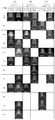
이하, 본 발명의 바람직한 실시 예들을 도 1 내지 도 8를 참조하여 상세하게 설명하기로 한다.Hereinafter, preferred embodiments of the present invention will be described in detail with reference to FIGS. 1 to 8. FIG.
도 1은 본 발명에 따른 와이어 그리드 편광자의 작용 원리를 나타낸 사시도이고, 도 2는 도 1에 도시된 와이어 그리드 편광자의 제1 및 제2 격자 각각의 높이 및 폭을 설명하기 위한 단면도이다. FIG. 1 is a perspective view illustrating the principle of operation of the wire grid polarizer according to the present invention, and FIG. 2 is a cross-sectional view illustrating the height and width of each of the first and second grids of the wire grid polarizer shown in FIG.
도 1에 도시된 바와 같이 와이어 그리드 편광자는 기판 상에 소정 간격으로 나란하게 배치되는 다수개의 와이어 그리드를 포함한다. 이러한, 와이어 그리드 편광자는 와이어 그리드 간 간격, 즉 피치(pitch)가 입사광의 파장보다 충분히 작을 경우 비편광 상태의 빛이 입사될 때 전도성의 와이어 그리드와 직교하는 벡터를 가지는 성분, 즉 P 편광은 투과하고 와이어 그리드와 평행한 벡터를 가지는 성분, 즉 S 편광은 반사시키게 된다.As shown in Fig. 1, the wire grid polarizers include a plurality of wire grids arranged on a substrate at regular intervals. The wire grid polarizer is a component that has a vector orthogonal to the conductive wire grid when light in the unpolarized state is incident when the pitch between the wire grids is sufficiently smaller than the wavelength of the incident light, And reflects a component having a vector parallel to the wire grid, that is, S polarized light.
다수개의 와이어 그리드는 적어도 두 개층으로 형성되며, 도 1에 도시된 바와 같이 기판(100) 상에 소정의 간격으로 나란하게 배치되는 제1 격자(110)와, 제1 격자(110) 상에 형성된 제2 격자(112)를 포함한다. The plurality of wire grids are formed of at least two layers, and each of the plurality of wire grids has a
와이어 그리드 편광자의 광학 특성은 제1 및 제2 격자(110,112) 각각의 폭(C,F), 높이(D,E)에 따라 또는 제2 격자 간의 거리(A)에 따라 달라지게 된다. 즉, 와이어 그리드 편광자의 광학 특성은 동일 격자의 높이 및 폭으로 형성할 경우에 격자 간의 거리가 감소할수록 휘도가 증가되며, 동일 격자 간의 거리에서는 격자의 높이가 낮을수록 격자 폭이 좁아질수록 휘도가 높아지게 된다. 또한, 동일 격자 간의 거리 및 동일 격자의 폭으로 형성될 경우에는 격자 높이가 높을수록 휘도가 높게 나타나게 된다. The optical characteristics of the wire grid polarizer depend on the widths C and F of the first and
그리고, 최대의 편광 효율을 확보하기 위해서는 격자 간의 거리가 감소할 수 록 편광 특성이 증가되며, 동일 격자 간의 거리 및 동일 격자의 폭으로 형성할 경우에 격자 높이가 증가할수록 편광 특성이 증가되며, 동일 격자 간의 거리 및 동일 격자의 높이로 형성할 경우에 격자의 폭이 증가할수록 편광 특성이 향상된다. In order to secure the maximum polarization efficiency, the polarization characteristics are increased as the distance between the gratings decreases. When the distance between the gratings and the width of the same grating are increased, the polarization characteristics increase as the grating height increases. When the distance between the gratings and the height of the same grating are increased, the polarization characteristics are improved as the width of the grating increases.
이와 같이, 최대의 휘도를 얻기 위해서는 최적의 격자 높이와 폭을 조정하여 형성하여야 한다. 위에서 설명한 조건을 고려하여, 제1 및 제2 격자(110,112) 각각의 폭(C,F), 높이(D,E) 또는 와이어 간의 거리(A)를 하기와 같이 형성할 수 있다. 또한, 도 2 및 도 4에 도시된 B는 제2 격자 간의 폭을 의미하며, G는 제1 격자 간의 폭을 의미한다. Thus, in order to obtain the maximum luminance, it is necessary to adjust the optimum lattice height and width. The width (C, F), the height (D, E) of each of the first and
제1 격자(110)는 기판(100) 상에 폴리머 재질로 형성되며, 스트라이프, 곡선, 사각형, 삼각형 등의 다양한 형상으로 형성될 수 있다. 제1 격자(110)는 광학 특성인 투과율, 휘도, 편광효율을 고려하여 제1 격자(110)의 높이(E) 및 폭(F)은 5nm~500㎛로 형성될 수 있다. 구체적으로, 제2 격자(112) 간의 거리(A)가 10nm~1㎛로 형성되며, 제1 격자(110)의 높이(E) 및 폭(F)이 5nm~500㎛로 형성될 경우에, 제2 격자(112) 간의 거리(A)와 제1 격자(110) 폭(F)의 비율은 1 : 0.2~0.9의 비율을 가지도록 형성되며, 제2 격자(112) 간의 거리(A)와 제1 격자(110) 높이(E)의 비율은 1 : 0.5~1.2의 비율을 가지도록 형성될 수 있다. The
제2 격자(112)는 제1 격자(110) 상에 금속 재질로 형성되며, 스트라이프, 곡선, 사각형, 삼각형 등의 다양한 형상으로 형성될 수 있다. 제2 격자(112)는 광학 특성인 투과율, 휘도, 편광효율을 고려하여 제2 격자(112)의 높이(D) 및 폭(C)은 100nm~350nm로 형성될 수 있다. 구체적으로, 제2 격자(112) 간의 거리(A)가 10nm~1㎛로 형성되며, 제2 격자(112)의 높이(D) 및 폭(C)이 100nm~350nm로 형성될 경우에, 제2 격자(112) 간의 거리(A)와 제2 격자(112) 폭(C)의 비율은 1 : 0.5~1.5의 비율을 가지도록 형성되며, 제2 격자(112) 간의 거리(A)와 제2 격자(112) 높이(D)의 비율은 1 : 0.5~2.5의 비율을 가지도록 형성될 수 있다. The
도 6은 제2 격자의 높이 및 폭에 따른 투과율을 나타내는 도면이다. 6 is a graph showing the transmittance according to the height and width of the second grating.
도 6에서 (a)는 제2 격자(112)의 높이(D)를 100~150nm로 형성되며, 제2 격자(112) 간의 거리(A)를 100~200nm로 형성될 경우에 제2 격자(112)의 폭(C)을 좁게함에 따른 투과율을 나타내고 있으며, (b)는 제2 격자(112)의 높이(D)를 151~200nm로 형성되며, 제2 격자(112) 간의 거리(A)를 100~200nm로 형성될 경우에 제2 격자(112)의 폭(C)을 좁게함에 따른 투과율을 나타내고 있으며, (c)는 제2 격자(112)의 높이(D)를 201~300nm로 형성되며, 제2 격자(112)간의 거리(A)를 100~200nm로 형성될 경우에 제2 격자(112)의 폭(C)을 좁게함에 따른 투과율을 나타내고 있다. 즉, 도 6(a)(b)(c)와 같이 제2 격자(112)의 높이(D)를 일정하게 하고, 제2 격자(112)의 폭(C)을 점차 좁게 할수록 투과율이 향상됨을 알 수 있다. 6A shows a case where the height D of the
예로 들어, 도 7에 도시된 바와 같이 투과율이 40~60%일 경우에, 바람직하게는 50%일 경우에 높은 휘도를 나타낸다. 따라서, 본 발명에 따른 제1 및 제2 격자(110,112)의 높이(D,E) 및 폭(C,F) 또는 제2 격자(112) 간의 거리(A)로 형성될 경우에 높은 투과율을 나타냄을 알 수 있다.For example, as shown in FIG. 7, a high luminance is exhibited when the transmittance is 40 to 60%, preferably 50%. Therefore, when the first and
또한, 표 1은 본 발명의 제2 격자(112) 간의 거리(A)에 따른 투과율 및 편광 효율을 나타내고 있다.Table 1 shows the transmittance and the polarization efficiency according to the distance A between the
도 3a 내지 도 3c는 본 발명에 따른 와이어 그리드 편광자의 제조 방법을 나타낸 사시도들이다. 여기서, 본 발명에 따른 와이어 그리드 편광자는 제1 격자 및 제2 격자가 스트라이프 형태로 형성되는 것을 예로 들어 설명하기로 한다. 3A to 3C are perspective views illustrating a method of manufacturing a wire grid polarizer according to the present invention. Here, the wire grid polarizer according to the present invention will be described by taking as an example that the first lattice and the second lattice are formed in a stripe form.
도 3a는 도시된 바와 같이 기판(100) 상에 폴리머 재질인 예로 들어 UV 레진(resin)(122)이 도포된다. 이어서, UV 레진(122)이 도포된 기판(100) 상부에 홈(126)과 돌출부(128)를 가지는 임프린트용 몰드(120)가 정렬된다. 여기서, 임프린트용 몰드(120)의 다수개의 홈(126) 및 돌출부(128)는 서로 일정 간격 이격된 형태로 반복하여 형성된다. 또한, 임프린트용 몰드(120)의 홈(126)은 제1 격자(110)가 형성될 위치와 대응된다. 이때, 임프린트용 몰드(120)의 홈(126)의 높이 및 폭은 5nm~500㎛로 형성될 수 있다. 또한, 임프린트용 몰드(120)의 홈(126)의 폭과 제2 격자(112) 간의 거리의 비율은 1 : 0.2~0.9로 형성되도록하며, 임프린트용 몰드(120)의 홈(126)의 높이와 제2 격자(112) 간의 거리의 비율은 1 : 0.5~1.2로 형성되도록 한다. 임프린트용 몰드(120)의 홈(126)은 스트라이프 형태로 형성된다. 임프린트용 몰드(120)는 임프린트용 몰드(120)의 홈(126) 부분과 폴리머 재질(122)이 접촉되도록 폴리머 재질(122)을 가압시킨 뒤, UV를 조사한다. 이에 따라, 폴리머 재질(122)은 임프린트용 몰드(120)의 홈(126)과 대응되는 부분에 높이(E) 및 폭(F)이 5nm~500㎛로 형성된 다수의 제1 격자(110)가 형성된다. 3A, a polymeric material, such as
그런 다음, 도 3b에 도시된 바와 같이 다수의 제1 격자(110)가 형성된 기판(100) 상에 금속층(124)을 증착한 뒤, 도 3c와 같이 금속층(124)을 식각 공정하여 제1 격자(110) 상에 제2 격자(112)를 형성한다. 3B, a
구체적으로, 다수의 제1 격자(110)가 형성된 기판(100) 상에 증착된 금속층(124)을 습식 식각 공정을 통해 높이 및 폭이 100nm~350nm인 제2 격자(112)를 형성한다. 또한, 습식 식각 공정시 제2 격자(112) 간의 거리와 제2 격자(112)의 높이의 비율은 1 : 0.5~2.5로 형성되도록 하며, 제2 격자(112) 간의 거리와 제2 격자(112)의 폭의 비율은 1 : 0.5~0.9로 형성되도록 한다. 이 결과, 기판(100) 상에 제1 격자(110) 상에 제2 격자(112)가 형성된 와이어 그리드 편광자가 형성된다. Specifically, the
이렇게 도 3a 내지 도 3c에 도시된 바와 같이 임프린트 공정, 증착 공정, 습식 식각 공정만을 통해 제1 및 제2 격자(110,112)가 포함된 와이어 그리드 편광자를 형성할 수 있다. 즉, 제조 공정 과정을 줄임으로써 공정 비용 절감 효과 및 대량 양산에 적용할 수 있다. As shown in FIGS. 3A to 3C, the wire grid polarizer including the first and
한편, 도 4는 와이어 그리드 편광자의 제1 격자(140)가 스트라이프 형태가 아닌, 반원 형태의 곡선을 가졌을 경우를 나타내는 단면도이고, 도 5a 내지 도 5c는 도 4에 도시된 와이어 그리드 편광자의 제조 방법을 설명하기 위한 도면으로 이밖에 도 2, 도 3a 내지 도 3c와 동일한 공정 및 동일한 구조를 가지므로 생략하기로 한다.FIG. 4 is a cross-sectional view showing a case where the
도 8은 본 발명의 실시 예에 따른 액정 표시 장치를 나타낸 단면도이다. 8 is a cross-sectional view illustrating a liquid crystal display device according to an embodiment of the present invention.
도 8를 참조하면, 본 발명의 실시 예에 따른 액정 표시 장치는 액정 표시 패널(200)과, 액정 표시 패널(200)에 광을 공급하는 백라이트 유닛(230)과, 액정 표시 패널(200)의 상/하부 또는 백라이트 유닛에 포함된 광학 시트 중 어느 한 면에 패터닝되어 형성된 와이어 그리드 편광자를 포함한다.8, a liquid crystal display according to an exemplary embodiment of the present invention includes a liquid
백라이트 유닛(230)은 광원(232)과, 그 광원(232)으로부터의 광을 확산시키는 확산시트(236)와, 광원(232)의 하부에 설치된 반사시트(234)를 포함한다.The
광원(132)은 냉음극 형광 램프(Cold Cathode Fluorescent Lamp : CCFL), 외부 전극 형광 램프(External Electrode Fluorescent : EEFL), 발광 다이오드(Light Emitting Diode; LED) 중 어느 하나로 형성될 수 있다. 이러한 광원(232)은 광을 생성하여 그 광을 확산시트(236)쪽으로 출사시킨다.The light source 132 may be formed of any one of a cold cathode fluorescent lamp (CCFL), an external electrode fluorescent lamp (EEFL), and a light emitting diode (LED). The
반사 시트(234)는 반사효율의 높은 재질로 형성되어 액정 표시 패널(200)의 반대방향으로 진행하는 광을 확산시트(236)쪽으로 반사시켜 광손실을 줄이는 역할을 한다. The
확산 시트(236)는 광원(132)으로부터 입사된 광을 액정 표시 패널(100)의 정면으로 향하게 하고, 넓은 범위에서 균일한 분포를 가지도록 광을 확산시켜 액정 표시 패널(100)에 조사되게 한다. 이러한 확산 시트(136)로는 양면에 소정의 광 확산용 부재가 코팅된 투명수지로 구성된 필름을 사용하는 것이 바람직하다. The
액정 표시 패널(200)은 칼러 필터 기판(212)과, 액정층(202)을 사이에 두고 칼러 필터 기판(212)과 대향하여 합착된 박막 트랜지스터 기판(210)과, 칼러 필터 기판(212)과 박막 트랜지스터 기판(210)를 포함한다. The liquid
칼러 필터 기판(212)에는 빛샘 방지를 위한 블랙 매트릭스와, 칼러 구현을 위한 칼러 필터, 화소전극과 수직전계를 이루는 공통전극과, 그들 위에 액정 배향을 위해 도포된 상부 배향막을 포함하는 칼라 필터 어레이가 상부기판 상에 형성된다.In the
박막 트랜지스터 기판(210)에는 서로 교차되게 형성된 게이트라인 및 데이터라인과, 그들의 교차부에 형성된 박막트랜지스터와, 박막트랜지스터와 접속된 화소전극과, 그들 위에 액정 배향을 위해 도포된 하부 배향막을 포함하는 박막트랜지스터 어레이가 하부 기판 상에 형성된다. The thin
와이어 그리드 편광자는 도 8에 도시된 바와 같이 액정 표시 패널(120)의 하부에 형성될 수 있으며, 액정 표시 패널(200)의 상부면 또는 백라이트 유닛(230)에 포함된 광학 시트 중 어느 한면에 형성될 수 있다. 와이어 그리드 편광자는 액정 표시 패널(200)의 하부면에 소정의 간격으로 나란하게 배치되는 제1 격자(110)와, 제1 격자(110) 상에 형성된 제2 격자(112)를 포함한다. 이 밖에 와이어 그리드 편광자의 제1 및 제2 격자(110,112)는 도 1 내지 도 3c의 설명과 동일하므로 생략하기로 한다. The wire grid polarizer may be formed on the lower surface of the liquid
이상에서 설명한 본 발명의 상세한 설명에서는 본 발명의 바람직한 실시 예를 참조하여 설명하였지만, 해당 기술 분야의 숙련된 당업자 또는 해당 기술 분야에 통상의 지식을 갖는 자라면, 후술된 특허청구범위에 기재된 본 발명의 사상 및 기술 영역으로부터 벗어나지 않는 범위 내에서 본 발명을 다양하게 수정 및 변경시킬 수 있음을 이해 할 수 있을 것이다. While the present invention has been described in connection with what is presently considered to be practical exemplary embodiments, it is to be understood that the invention is not limited to the disclosed embodiments, but, on the contrary, It will be understood by those skilled in the art that various changes in form and details may be made therein without departing from the spirit and scope of the invention.
따라서, 본 발명의 기술적 범위는 명세서의 상세한 설명에 기재된 내용으로 한정되는 것이 아니라 특허 청구 범위에 의해 정하여져야만 할 것이다. Therefore, the technical scope of the present invention should not be limited to the contents described in the detailed description of the specification, but should be defined by the claims.
도 1은 본 발명에 따른 와이어 그리드 편광자의 작용 원리를 나타낸 사시도이다.1 is a perspective view showing the principle of operation of a wire grid polarizer according to the present invention.
도 2는 도 1에 도시된 와이어 그리드 편광자의 제1 및 제2 격자 각각의 높이 및 폭을 설명하기 위한 단면도이다. 2 is a cross-sectional view illustrating the height and width of each of the first and second gratings of the wire grid polarizer shown in FIG.
도 3a 내지 도 3c는 본 발명에 따른 와이어 그리드 편광자의 제조 방법을 나타낸 사시도들이다.3A to 3C are perspective views illustrating a method of manufacturing a wire grid polarizer according to the present invention.
도 4는 본 발명에 따른 제1 격자의 패턴이 반구 형태로 형성된 와이어 그리드 편광자를 나타낸 단면도이다.4 is a cross-sectional view showing a wire grid polarizer in which a pattern of a first lattice is formed in a hemispherical shape according to the present invention.
도 5a 내지 도 5c는 도 4에 도시된 와이어 그리드 편광자의 제조 방법을 나타낸 사시도들이다.5A to 5C are perspective views illustrating a method of manufacturing the wire grid polarizer shown in FIG.
도 6은 본 발명에 따른 와이어 그리드 편광자의 제2 격자의 높이 및 폭에 따른 투과율을 나타내는 도면이다. 6 is a graph showing the transmittance according to the height and width of the second grating of the wire grid polarizer according to the present invention.
도 7은 투과율 및 휘도를 나타내는 그래프이다.7 is a graph showing transmittance and luminance.
도 8은 본 발명의 실시 예에 따른 액정 표시 장치를 나타낸 단면도이다. 8 is a cross-sectional view illustrating a liquid crystal display device according to an embodiment of the present invention.
<도면의 주요 부분에 대한 부호의 설명>Description of the Related Art
100 : 기판 110,140 : 제1 격자100: substrate 110,140: first lattice
112,142 : 제2 격자 120 : 임프린트용 몰드112, 142: second grating 120: mold for imprint
124 : 금속층 200 : 액정 표시 패널124: metal layer 200: liquid crystal display panel
230 : 백라이트 유닛230: Backlight unit
Claims (16)
Priority Applications (5)
| Application Number | Priority Date | Filing Date | Title |
|---|---|---|---|
| KR1020090031463A KR101610376B1 (en) | 2009-04-10 | 2009-04-10 | A wire grid polarizer, liquid crystal display including the same and method of manufacturing the wire grid polarizer |
| CN2010800162627A CN102549482A (en) | 2009-04-10 | 2010-04-12 | Wire grid polarizer, LCD device including the same, 3D stereoscopic image display device, and manufacturing method of wire grid polarizer |
| US13/263,814 US9599762B2 (en) | 2009-04-10 | 2010-04-12 | Wire grid polarizer, liquid crystal device including the wire grid polarizer, 3-D stereoscopic image display device including the wire grid polarizer, and method of manufacturing the wire grid polarizer |
| PCT/KR2010/002236 WO2010117249A2 (en) | 2009-04-10 | 2010-04-12 | Wire grid polarizer, lcd device including the same, 3d stereoscopic image display device, and manufacturing method of wire grid polarizer |
| JP2012504626A JP2012523582A (en) | 2009-04-10 | 2010-04-12 | Wire grid polarizer, liquid crystal display device including the same, three-dimensional stereoscopic image display device, and method of manufacturing wire grid polarizer |
Applications Claiming Priority (1)
| Application Number | Priority Date | Filing Date | Title |
|---|---|---|---|
| KR1020090031463A KR101610376B1 (en) | 2009-04-10 | 2009-04-10 | A wire grid polarizer, liquid crystal display including the same and method of manufacturing the wire grid polarizer |
Publications (2)
| Publication Number | Publication Date |
|---|---|
| KR20100112926A KR20100112926A (en) | 2010-10-20 |
| KR101610376B1 true KR101610376B1 (en) | 2016-04-08 |
Family
ID=42936752
Family Applications (1)
| Application Number | Title | Priority Date | Filing Date |
|---|---|---|---|
| KR1020090031463A Expired - Fee Related KR101610376B1 (en) | 2009-04-10 | 2009-04-10 | A wire grid polarizer, liquid crystal display including the same and method of manufacturing the wire grid polarizer |
Country Status (5)
| Country | Link |
|---|---|
| US (1) | US9599762B2 (en) |
| JP (1) | JP2012523582A (en) |
| KR (1) | KR101610376B1 (en) |
| CN (1) | CN102549482A (en) |
| WO (1) | WO2010117249A2 (en) |
Families Citing this family (34)
| Publication number | Priority date | Publication date | Assignee | Title |
|---|---|---|---|---|
| CN102834749B (en) * | 2010-03-30 | 2015-02-04 | 日本电气株式会社 | Optical element, light source device, and projection display device |
| KR20130118729A (en) * | 2010-04-27 | 2013-10-30 | 더 리젠츠 오브 더 유니버시티 오브 미시건 | Display device having plasmonic color filters and photovoltaic capabilities |
| KR20120032776A (en) * | 2010-09-29 | 2012-04-06 | 엘지이노텍 주식회사 | A wire grid polarizer and backlightounit uaing the same |
| KR101319444B1 (en) * | 2010-10-20 | 2013-10-17 | 엘지이노텍 주식회사 | Liquid Crystal Display within a wire grid polarazer |
| US20150077851A1 (en) * | 2010-12-30 | 2015-03-19 | Moxtek, Inc. | Multi-layer absorptive wire grid polarizer |
| US8552439B2 (en) * | 2011-04-07 | 2013-10-08 | Himax Display, Inc. | Light-emitting diode package |
| EP2699952A4 (en) | 2011-04-20 | 2015-06-24 | Univ Michigan | SPECTRAL FILTERING FOR VISUAL DISPLAYS AND IMAGING SYSTEM HAVING MINIMUM ANGULAR DEPENDENCY |
| KR101775163B1 (en) * | 2011-07-28 | 2017-09-05 | 엘지이노텍 주식회사 | Manufacturing method of mold for nano imprint and mold for nano imprint by using the same |
| FR2994602B1 (en) * | 2012-08-16 | 2014-09-12 | Commissariat Energie Atomique | SPECTRAL FILTERING DEVICE IN VISIBLE AND INFRARED DOMAINS |
| KR20140030382A (en) | 2012-08-27 | 2014-03-12 | 삼성디스플레이 주식회사 | Liquid crystal display and fabrication method of the same |
| US9261730B2 (en) * | 2013-01-03 | 2016-02-16 | Empire Technology Development Llc | Display devices including inorganic components and methods of making and using the same |
| US9547107B2 (en) | 2013-03-15 | 2017-01-17 | The Regents Of The University Of Michigan | Dye and pigment-free structural colors and angle-insensitive spectrum filters |
| AU2013100685B4 (en) * | 2013-05-21 | 2013-09-12 | Innovia Security Pty Ltd | Optical device including vertical pixels |
| JP5929860B2 (en) | 2013-09-24 | 2016-06-08 | ウシオ電機株式会社 | Grid polarizing element manufacturing method |
| WO2015060943A1 (en) * | 2013-10-24 | 2015-04-30 | Moxtek, Inc. | Polarizer with variable inter-wire distance |
| US9354374B2 (en) * | 2013-10-24 | 2016-05-31 | Moxtek, Inc. | Polarizer with wire pair over rib |
| US10447040B2 (en) | 2014-10-15 | 2019-10-15 | Cummins Power Generation Ip, Inc. | Programmable inverter for controllable grid response |
| KR20160049162A (en) * | 2014-10-24 | 2016-05-09 | 삼성디스플레이 주식회사 | A method of manufacturing a mold and a method of manufacturing a polarizer |
| KR20170062590A (en) * | 2015-11-27 | 2017-06-08 | 삼성디스플레이 주식회사 | Wire grid polarizer plate and method for manufacturing the smae |
| KR102567008B1 (en) * | 2016-03-18 | 2023-08-14 | 삼성디스플레이 주식회사 | Display devic including wire grid polarizer and manufacturing method thereof |
| JP6720625B2 (en) * | 2016-03-25 | 2020-07-08 | 大日本印刷株式会社 | Polarizer and method for manufacturing polarizer |
| JP6230689B1 (en) * | 2016-12-28 | 2017-11-15 | デクセリアルズ株式会社 | Polarizing plate, method for producing the same, and optical instrument |
| CN107167863B (en) * | 2017-07-07 | 2019-09-10 | 深圳市华星光电技术有限公司 | The production method of nanometer wiregrating polaroid |
| KR102137548B1 (en) * | 2017-09-07 | 2020-07-24 | 삼성에스디아이 주식회사 | Polarizing plate and optical display apparatus comprising the same |
| TWI641878B (en) | 2017-09-22 | 2018-11-21 | 友達光電股份有限公司 | Wire grid polarizer and display panel using the same |
| JP7226936B2 (en) * | 2018-07-26 | 2023-02-21 | デクセリアルズ株式会社 | Polarizing plate and optical equipment |
| US20200041807A1 (en) * | 2018-08-02 | 2020-02-06 | Christie Digital Systems Usa, Inc. | Light emitting diode display with a monolithic wire-grid polarizer for producing three-dimensional images |
| CN109031507B (en) * | 2018-08-15 | 2020-01-24 | 京东方科技集团股份有限公司 | Light guide plate and its manufacturing method, backlight module and display device |
| US12235389B2 (en) * | 2018-08-31 | 2025-02-25 | Magna Electronics Inc. | Automotive radar / LIDAR behind reflective surfaces |
| PH12020050192B1 (en) * | 2019-07-17 | 2023-12-01 | Moxtek Inc | Reflective wire grid polarizer with transparent cap |
| CN113933924A (en) * | 2020-06-29 | 2022-01-14 | 京东方科技集团股份有限公司 | Wire grid polarizer, method for making the same, and display device |
| CN113867032A (en) | 2020-06-30 | 2021-12-31 | 京东方科技集团股份有限公司 | A kind of wire grid polarizer and its manufacturing method |
| KR102703701B1 (en) * | 2021-11-02 | 2024-09-05 | 한국과학기술원 | Nickel stamp and Method of manufacturing the same |
| CN116053288B (en) * | 2023-01-28 | 2023-06-13 | 合肥晶合集成电路股份有限公司 | Image sensor and manufacturing method thereof |
Citations (1)
| Publication number | Priority date | Publication date | Assignee | Title |
|---|---|---|---|---|
| WO2007116972A1 (en) | 2006-04-07 | 2007-10-18 | Asahi Glass Company, Limited | Wire grid polarizer and method for producing the same |
Family Cites Families (27)
| Publication number | Priority date | Publication date | Assignee | Title |
|---|---|---|---|---|
| US3293331A (en) * | 1962-11-13 | 1966-12-20 | Little Inc A | Method of forming replicas of contoured substrates |
| JP2002328222A (en) * | 2001-04-26 | 2002-11-15 | Nippon Sheet Glass Co Ltd | Polarizing element and method for manufacturing the same |
| CN100592112C (en) * | 2002-02-12 | 2010-02-24 | 奥尔利康贸易股份公司(特吕巴赫) | Component comprising sub-micron hollow spaces |
| US6665119B1 (en) * | 2002-10-15 | 2003-12-16 | Eastman Kodak Company | Wire grid polarizer |
| TWI256491B (en) * | 2004-07-27 | 2006-06-11 | Pavonine Inc | Liquid crystal display device having thin polarizing film and thin phase retardation film |
| KR100483352B1 (en) * | 2004-07-27 | 2005-04-14 | (주)파버나인 | Liquid crystal display device using thin film polarizers and retarders |
| JP4442760B2 (en) * | 2004-08-06 | 2010-03-31 | 旭化成イーマテリアルズ株式会社 | Inorganic material selective pattern forming method and grid-type polarizing element |
| US20060056024A1 (en) * | 2004-09-15 | 2006-03-16 | Ahn Seh W | Wire grid polarizer and manufacturing method thereof |
| US7961393B2 (en) * | 2004-12-06 | 2011-06-14 | Moxtek, Inc. | Selectively absorptive wire-grid polarizer |
| US7570424B2 (en) * | 2004-12-06 | 2009-08-04 | Moxtek, Inc. | Multilayer wire-grid polarizer |
| WO2006064693A1 (en) * | 2004-12-16 | 2006-06-22 | Toray Industries, Inc. | Polarizing plate, method of producing the polarizing plate, and liquid crystal display device using the polarizing plate |
| KR100656999B1 (en) * | 2005-01-19 | 2006-12-13 | 엘지전자 주식회사 | Method of manufacturing mold for manufacturing lattice of line lattice polarizing film and line lattice polarizing film |
| KR100894939B1 (en) | 2005-10-17 | 2009-04-27 | 아사히 가세이 가부시키가이샤 | Wire grid polarizer and manufacturing method of the same |
| WO2008022099A2 (en) * | 2006-08-15 | 2008-02-21 | Api Nanofabrication And Research Corp. | Polarizer films and methods of making the same |
| US8755113B2 (en) * | 2006-08-31 | 2014-06-17 | Moxtek, Inc. | Durable, inorganic, absorptive, ultra-violet, grid polarizer |
| JP4520445B2 (en) * | 2006-10-11 | 2010-08-04 | 旭化成イーマテリアルズ株式会社 | Wire grid polarizer |
| JP4778873B2 (en) | 2006-10-20 | 2011-09-21 | 株式会社 日立ディスプレイズ | Liquid crystal display |
| JP2008181113A (en) * | 2006-12-27 | 2008-08-07 | Toray Ind Inc | Reflection type polarizer and liquid crystal display device |
| US8027086B2 (en) * | 2007-04-10 | 2011-09-27 | The Regents Of The University Of Michigan | Roll to roll nanoimprint lithography |
| JP5069036B2 (en) * | 2007-04-16 | 2012-11-07 | 旭化成イーマテリアルズ株式会社 | Polarizing plate with high degree of polarization |
| KR100922186B1 (en) | 2007-06-18 | 2009-10-19 | 미래나노텍(주) | Method of manufacturing wire grid polarizer |
| KR100980284B1 (en) | 2007-09-07 | 2010-09-06 | 미래나노텍(주) | Nanowire grid polarizer with improved adhesion and manufacturing method |
| JP2009075265A (en) * | 2007-09-19 | 2009-04-09 | Nippon Zeon Co Ltd | Manufacturing method of grid polarizing film |
| KR101457254B1 (en) | 2007-09-28 | 2014-10-31 | 아사히 가라스 가부시키가이샤 | Photocurable composition, method for producing fine patterned body, and optical device |
| JP5206029B2 (en) | 2008-03-04 | 2013-06-12 | ソニー株式会社 | Liquid crystal display |
| KR100952137B1 (en) | 2008-04-18 | 2010-04-09 | 실리콘 디스플레이 (주) | Stereoscopic image display device and manufacturing method thereof |
| KR20110031440A (en) | 2008-07-10 | 2011-03-28 | 아사히 가라스 가부시키가이샤 | Wire grid polarizer and its manufacturing method |
-
2009
- 2009-04-10 KR KR1020090031463A patent/KR101610376B1/en not_active Expired - Fee Related
-
2010
- 2010-04-12 JP JP2012504626A patent/JP2012523582A/en active Pending
- 2010-04-12 CN CN2010800162627A patent/CN102549482A/en active Pending
- 2010-04-12 US US13/263,814 patent/US9599762B2/en not_active Expired - Fee Related
- 2010-04-12 WO PCT/KR2010/002236 patent/WO2010117249A2/en not_active Ceased
Patent Citations (1)
| Publication number | Priority date | Publication date | Assignee | Title |
|---|---|---|---|---|
| WO2007116972A1 (en) | 2006-04-07 | 2007-10-18 | Asahi Glass Company, Limited | Wire grid polarizer and method for producing the same |
Also Published As
| Publication number | Publication date |
|---|---|
| CN102549482A (en) | 2012-07-04 |
| US9599762B2 (en) | 2017-03-21 |
| US20120086887A1 (en) | 2012-04-12 |
| JP2012523582A (en) | 2012-10-04 |
| WO2010117249A2 (en) | 2010-10-14 |
| KR20100112926A (en) | 2010-10-20 |
| WO2010117249A3 (en) | 2011-01-20 |
Similar Documents
| Publication | Publication Date | Title |
|---|---|---|
| KR101610376B1 (en) | A wire grid polarizer, liquid crystal display including the same and method of manufacturing the wire grid polarizer | |
| TW515921B (en) | Reflective liquid crystal display apparatus | |
| KR102176591B1 (en) | Wire grid polarizer, liquid crystal display having the same and method of manufacturing the same | |
| US7944544B2 (en) | Liquid crystal device having a diffraction function layer that includes a flat portion and a non-flat portion with a grid disposed in the non-flat portion | |
| EP2894511B1 (en) | In-cell polariser, liquid crystal display including it and method of manufacturing the liquid crystal display | |
| KR20100035783A (en) | Polarizer, method for manufacturing the same, display substrate and black light asamble having the polarizer | |
| US9080748B2 (en) | Display panel having improved light-use efficiency, display device including the display panel, and method of manufacturing the display panel | |
| KR101714035B1 (en) | A wire grid polarizer, liquid crystal display, 3d-display including the same and method of manufacturing the wire grid polarizer | |
| KR20120050645A (en) | Liquid crystal display and manufacturing method thereof | |
| US20150070762A1 (en) | Polarizer, display device having the same, and method of manufacturing the same | |
| JP2009015305A (en) | Optical element and projection display device | |
| KR20130024041A (en) | A wire grid polarizer, liquid crystal display including the same and method of manufacturing the wire grid polarizer | |
| JP2009015302A (en) | Optical element, liquid crystal device, electronic device, method for manufacturing optical element, method for manufacturing liquid crystal device | |
| KR20130126391A (en) | Method for fabricating wire grid polarizer and wire grid polarizer using the method thereof | |
| KR102079163B1 (en) | Wire grid polarizer, display device including the same and method for fabricating the same | |
| JP3974787B2 (en) | Reflective liquid crystal display | |
| KR100707083B1 (en) | Line lattice polarizer and its manufacturing method | |
| US9594206B2 (en) | Complex substrate for display apparatus, display apparatus having the same and method of manufacturing the same | |
| KR102255379B1 (en) | Display device and method of manufacturing the same | |
| TWI743680B (en) | Polarizer substrate and manufacturing method thereof | |
| KR20150113438A (en) | Method for fabricating wire grid polarizer | |
| KR20110107694A (en) | Nano wire grid polarizer and liquid crystal display device comprising the same | |
| TWI615765B (en) | Touch sensing substrate, and integrated structure having functions of polarization and touch-sensing | |
| KR20170017556A (en) | Wire grid polarizer and liquid crystal display device including the same | |
| KR100654243B1 (en) | Backlight unit |
Legal Events
| Date | Code | Title | Description |
|---|---|---|---|
| PA0109 | Patent application |
St.27 status event code: A-0-1-A10-A12-nap-PA0109 |
|
| N231 | Notification of change of applicant | ||
| PN2301 | Change of applicant |
St.27 status event code: A-3-3-R10-R13-asn-PN2301 St.27 status event code: A-3-3-R10-R11-asn-PN2301 |
|
| R18-X000 | Changes to party contact information recorded |
St.27 status event code: A-3-3-R10-R18-oth-X000 |
|
| PG1501 | Laying open of application |
St.27 status event code: A-1-1-Q10-Q12-nap-PG1501 |
|
| A201 | Request for examination | ||
| PA0201 | Request for examination |
St.27 status event code: A-1-2-D10-D11-exm-PA0201 |
|
| PN2301 | Change of applicant |
St.27 status event code: A-3-3-R10-R13-asn-PN2301 St.27 status event code: A-3-3-R10-R11-asn-PN2301 |
|
| E902 | Notification of reason for refusal | ||
| PE0902 | Notice of grounds for rejection |
St.27 status event code: A-1-2-D10-D21-exm-PE0902 |
|
| T11-X000 | Administrative time limit extension requested |
St.27 status event code: U-3-3-T10-T11-oth-X000 |
|
| E13-X000 | Pre-grant limitation requested |
St.27 status event code: A-2-3-E10-E13-lim-X000 |
|
| P11-X000 | Amendment of application requested |
St.27 status event code: A-2-2-P10-P11-nap-X000 |
|
| P13-X000 | Application amended |
St.27 status event code: A-2-2-P10-P13-nap-X000 |
|
| E902 | Notification of reason for refusal | ||
| PE0902 | Notice of grounds for rejection |
St.27 status event code: A-1-2-D10-D21-exm-PE0902 |
|
| P11-X000 | Amendment of application requested |
St.27 status event code: A-2-2-P10-P11-nap-X000 |
|
| P13-X000 | Application amended |
St.27 status event code: A-2-2-P10-P13-nap-X000 |
|
| R17-X000 | Change to representative recorded |
St.27 status event code: A-3-3-R10-R17-oth-X000 |
|
| E701 | Decision to grant or registration of patent right | ||
| PE0701 | Decision of registration |
St.27 status event code: A-1-2-D10-D22-exm-PE0701 |
|
| GRNT | Written decision to grant | ||
| PR0701 | Registration of establishment |
St.27 status event code: A-2-4-F10-F11-exm-PR0701 |
|
| PR1002 | Payment of registration fee |
St.27 status event code: A-2-2-U10-U11-oth-PR1002 Fee payment year number: 1 |
|
| PG1601 | Publication of registration |
St.27 status event code: A-4-4-Q10-Q13-nap-PG1601 |
|
| R18-X000 | Changes to party contact information recorded |
St.27 status event code: A-5-5-R10-R18-oth-X000 |
|
| R18-X000 | Changes to party contact information recorded |
St.27 status event code: A-5-5-R10-R18-oth-X000 |
|
| LAPS | Lapse due to unpaid annual fee | ||
| PC1903 | Unpaid annual fee |
St.27 status event code: A-4-4-U10-U13-oth-PC1903 Not in force date: 20190402 Payment event data comment text: Termination Category : DEFAULT_OF_REGISTRATION_FEE |
|
| PC1903 | Unpaid annual fee |
St.27 status event code: N-4-6-H10-H13-oth-PC1903 Ip right cessation event data comment text: Termination Category : DEFAULT_OF_REGISTRATION_FEE Not in force date: 20190402 |
|
| R18-X000 | Changes to party contact information recorded |
St.27 status event code: A-5-5-R10-R18-oth-X000 |
|
| PN2301 | Change of applicant |
St.27 status event code: A-5-5-R10-R13-asn-PN2301 St.27 status event code: A-5-5-R10-R11-asn-PN2301 |