CN102549482A - Wire grid polarizer, LCD device including the same, 3D stereoscopic image display device, and manufacturing method of wire grid polarizer - Google Patents
Wire grid polarizer, LCD device including the same, 3D stereoscopic image display device, and manufacturing method of wire grid polarizer Download PDFInfo
- Publication number
- CN102549482A CN102549482A CN2010800162627A CN201080016262A CN102549482A CN 102549482 A CN102549482 A CN 102549482A CN 2010800162627 A CN2010800162627 A CN 2010800162627A CN 201080016262 A CN201080016262 A CN 201080016262A CN 102549482 A CN102549482 A CN 102549482A
- Authority
- CN
- China
- Prior art keywords
- grid
- width
- ratio
- satisfies
- height
- Prior art date
- Legal status (The legal status is an assumption and is not a legal conclusion. Google has not performed a legal analysis and makes no representation as to the accuracy of the status listed.)
- Pending
Links
Images


Classifications
-
- G—PHYSICS
- G02—OPTICS
- G02B—OPTICAL ELEMENTS, SYSTEMS OR APPARATUS
- G02B5/00—Optical elements other than lenses
- G02B5/30—Polarising elements
-
- G—PHYSICS
- G02—OPTICS
- G02B—OPTICAL ELEMENTS, SYSTEMS OR APPARATUS
- G02B5/00—Optical elements other than lenses
- G02B5/30—Polarising elements
- G02B5/3025—Polarisers, i.e. arrangements capable of producing a definite output polarisation state from an unpolarised input state
- G02B5/3058—Polarisers, i.e. arrangements capable of producing a definite output polarisation state from an unpolarised input state comprising electrically conductive elements, e.g. wire grids, conductive particles
-
- G—PHYSICS
- G02—OPTICS
- G02F—OPTICAL DEVICES OR ARRANGEMENTS FOR THE CONTROL OF LIGHT BY MODIFICATION OF THE OPTICAL PROPERTIES OF THE MEDIA OF THE ELEMENTS INVOLVED THEREIN; NON-LINEAR OPTICS; FREQUENCY-CHANGING OF LIGHT; OPTICAL LOGIC ELEMENTS; OPTICAL ANALOGUE/DIGITAL CONVERTERS
- G02F1/00—Devices or arrangements for the control of the intensity, colour, phase, polarisation or direction of light arriving from an independent light source, e.g. switching, gating or modulating; Non-linear optics
- G02F1/01—Devices or arrangements for the control of the intensity, colour, phase, polarisation or direction of light arriving from an independent light source, e.g. switching, gating or modulating; Non-linear optics for the control of the intensity, phase, polarisation or colour
- G02F1/13—Devices or arrangements for the control of the intensity, colour, phase, polarisation or direction of light arriving from an independent light source, e.g. switching, gating or modulating; Non-linear optics for the control of the intensity, phase, polarisation or colour based on liquid crystals, e.g. single liquid crystal display cells
- G02F1/133—Constructional arrangements; Operation of liquid crystal cells; Circuit arrangements
- G02F1/1333—Constructional arrangements; Manufacturing methods
- G02F1/1335—Structural association of cells with optical devices, e.g. polarisers or reflectors
- G02F1/133528—Polarisers
-
- G—PHYSICS
- G02—OPTICS
- G02B—OPTICAL ELEMENTS, SYSTEMS OR APPARATUS
- G02B30/00—Optical systems or apparatus for producing three-dimensional [3D] effects, e.g. stereoscopic images
- G02B30/20—Optical systems or apparatus for producing three-dimensional [3D] effects, e.g. stereoscopic images by providing first and second parallax images to an observer's left and right eyes
- G02B30/22—Optical systems or apparatus for producing three-dimensional [3D] effects, e.g. stereoscopic images by providing first and second parallax images to an observer's left and right eyes of the stereoscopic type
- G02B30/25—Optical systems or apparatus for producing three-dimensional [3D] effects, e.g. stereoscopic images by providing first and second parallax images to an observer's left and right eyes of the stereoscopic type using polarisation techniques
-
- G—PHYSICS
- G02—OPTICS
- G02F—OPTICAL DEVICES OR ARRANGEMENTS FOR THE CONTROL OF LIGHT BY MODIFICATION OF THE OPTICAL PROPERTIES OF THE MEDIA OF THE ELEMENTS INVOLVED THEREIN; NON-LINEAR OPTICS; FREQUENCY-CHANGING OF LIGHT; OPTICAL LOGIC ELEMENTS; OPTICAL ANALOGUE/DIGITAL CONVERTERS
- G02F1/00—Devices or arrangements for the control of the intensity, colour, phase, polarisation or direction of light arriving from an independent light source, e.g. switching, gating or modulating; Non-linear optics
- G02F1/01—Devices or arrangements for the control of the intensity, colour, phase, polarisation or direction of light arriving from an independent light source, e.g. switching, gating or modulating; Non-linear optics for the control of the intensity, phase, polarisation or colour
- G02F1/13—Devices or arrangements for the control of the intensity, colour, phase, polarisation or direction of light arriving from an independent light source, e.g. switching, gating or modulating; Non-linear optics for the control of the intensity, phase, polarisation or colour based on liquid crystals, e.g. single liquid crystal display cells
- G02F1/133—Constructional arrangements; Operation of liquid crystal cells; Circuit arrangements
- G02F1/1333—Constructional arrangements; Manufacturing methods
- G02F1/1335—Structural association of cells with optical devices, e.g. polarisers or reflectors
- G02F1/133528—Polarisers
- G02F1/133548—Wire-grid polarisers
Landscapes
- Physics & Mathematics (AREA)
- Nonlinear Science (AREA)
- General Physics & Mathematics (AREA)
- Optics & Photonics (AREA)
- Mathematical Physics (AREA)
- Chemical & Material Sciences (AREA)
- Crystallography & Structural Chemistry (AREA)
- Polarising Elements (AREA)
Abstract
The present invention relates to a wire grid polarizer, an LCD device including the same, and a manufacturing method of the wire grid polarizer which can reduce the number of processes and obtain excellent brightness. According to the present invention, the wire grid polarizer, which comprises 1st grids arranged side by side on a substrate at fixed intervals and 2nd grids arranged on the 1st grids, can be formed only by an imprint process, a deposition process, and a wet-etching process, thereby decreasing the number of processes. Consequently, process costs and process time can be reduced, having an effect of obtaining reliability.
Description
Technical field
The present invention relates to the method for a kind of line grid polarizer that can obtain high brightness and reduce the technology number, the liquid-crystal apparatus that comprises line grid polarizer and manufacturing line grid polarizer.
Background technology
Usually, polarizer or polarizer are meant the optical element that extracts the straight line light polarization light with certain vibration direction from nonpolarized light such as natural light.A kind of as optical element, line grid polarizer is to utilize the conductive threads grid to produce the optical element of polarized light.Because line grid polarizer has the polarization separation characteristic higher than other polarizers, so it has been used as the reflective polarizer that can be used in the region of ultra-red wavelength coverage.
The technology that forms line grid polarizer comprises 6 to 7 processes, for example deposits metal in process, photoresist coating procedure, photoetching process, lithography development process, metal level etching process and photoresist stripping process on the base material.Correspondingly, the problem of life period and cost increase.
In addition, the most important factor of decision line grid polarizer performance is the relation between the interval between incident light wavelength and the line grid.That is to say, if the pitch of line grid is enough not little, then be difficult to obtain desired effects, reason is that incident light is not by polarization, but by diffraction.As stated, the key factor in the polarization characteristic of line grid polarizer comprises the pitch of line grid and the width and height of line grid.Yet, utilize width and the height of existing difficult technique with the control line grid.
Summary of the invention
Correspondingly; Keep it in mind the problems referred to above that occur in the prior art; Made the present invention, and an object of the present invention is to provide a kind of manufacturing approach, it forms line grid polarizer through only utilizing moulding process, deposition process and Wet-type etching process; Can reduce technology number, technology cost and time and guarantee reliability, said line grid polarizer comprises second grid that is arranged in parallel in first grid on the sheet material and on said first grid, forms with specific interval.
Especially, another object of the present invention provides line grid polarizer, and it comprises and only is configured to improve brightness through the Wet-type etching process and makes maximized second grid of polarization efficiency, can improve transmissivity thus.
According to an aspect of the present invention, a kind of line grid polarizer is provided, is included in first grid layer on the base material, said first grid layer comprises at least one first grid with particular sections distance and height; With second grid layer on said first grid, said second grid layer comprises at least one second grid with particular sections distance and height, and the width of wherein said first grid satisfies 1 with the ratio of the width of second grid: (0.2 to 1.5).
In this case, said first grid and said first grid layer of said line grid polarizer can be processed by polymeric material, and its second grid can be processed by metal material.
Especially; In said structure; The structure of said second grid can form and make the width of said second grid satisfy 1 for the ratio at the interval between said second grid: (0.2 to 1.5); The width of said second grid satisfies 1 with the ratio of the height of said second grid: (1 to 5), the pitch of perhaps said second grid satisfies 1 with the ratio of the height of said second grid: (1 to 5).
In addition, can form according to the line grid polarizer of said structure of the present invention and make the width of said first grid satisfy 1 for the ratio at the interval between said first grid: the width of (0.2 to 1.5) or said first grid satisfies 1 with the ratio of the height of said first grid: (0.2 to 5).
In this case, the pitch of the pitch of said second grid or said first grid can form 50nm to 1 μ m.
In addition, the xsect separately of first and second grids according to the present invention can be circle, ellipse or polygon.
Line grid polarizer with said structure can utilize following method to form.More specifically, manufacturing method according to the invention can comprise: first step: the first grid basal layer that is stacked on the base material through processing forms a plurality of first grids, and each all has the particular sections distance said a plurality of first grids; Second step: on said first grid, form the second grid basal layer; And third step: form a plurality of second grids through the said second grid basal layer of etching, the width of wherein said first grid satisfies 1 with the ratio of the width of said second grid: (0.2 to 1.5).
In this case, in said first step, can have the impressing mould of a plurality of grooves, in the zone corresponding, form a plurality of first grids on the said first grid basal layer of processing by polymeric material with said a plurality of grooves difference through extruding.
In addition, in said second step, can form the material layer of processing by metal material through depositing operation.
Especially; In above-mentioned manufacturing approach; In said first step, preferred said first grill-shaped becomes makes the width of said first grid satisfy 1 for the ratio at the interval between said first grid: the width of (0.2 to 1.5) or said first grid satisfies 1 with the ratio of the height of said first grid: (0.2 to 5).
In addition; In manufacturing method according to the invention; Can utilize the Wet-type etching process to carry out said third step; And can utilize etching process to carry out said third step makes the width of said second grid satisfy 1 for the ratio at the interval between said second grid: (0.2 to 1.5), the width of said second grid satisfies 1 with the ratio of the height of said second grid: (1 to 5), the pitch of perhaps said second grid satisfies 1 with the ratio of the height of said second grid: (1 to 5).
Line grid polarizer with said structure according to the present invention can be applicable to liquid-crystal apparatus.
More specifically, liquid-crystal apparatus can comprise LCD panel; Back light unit, it is configured to said LCD panel light is provided; With line grid polarizer according to the present invention, wherein said line grid polarizer is formed on the top or bottom of said LCD panel, perhaps is formed on arbitrary surface of a plurality of optical sheets that comprise in the said back light unit, and is configured to improve optical efficiency.
As stated, being included in line grid polarizer in the said liquid-crystal apparatus can form and make the width of said first grid satisfy 1 for the ratio at the interval between said first grid: the width of (0.2 to 1.5) or said first grid satisfies 1 with the ratio of the height of said first grid: (0.2 to 5).
Except above-mentioned liquid-crystal apparatus, line grid polarizer according to the present invention can also be applied to show the device of 3D stereo-picture.
Description of drawings
In conjunction with accompanying drawing, from the explanation of following preferred embodiment, above-mentioned and other purposes of the present invention and advantage will become obviously, in the accompanying drawing:
Fig. 1 is the stereographic map that shows the principle of work of line grid polarizer according to an embodiment of the invention;
Fig. 2 is first and second grids height separately and the viewgraph of cross-section of width that the line grid polarizer that shows among Fig. 1 is shown;
Fig. 3 is the figure that shows according to the transmissivity of the height of second grid of line grid polarizer of the present invention and width;
Fig. 4 is the figure that shows transmissivity and brightness;
Fig. 5 to 7 is the procedure charts that show according to the method for manufacturing line grid polarizer of the present invention;
Fig. 8 is the viewgraph of cross-section according to the line grid polarizer of first grid with hemispherical pattern of the present invention;
Fig. 9 to 11 is the stereographic maps that show the method for the line grid polarizer that shows in the shop drawings 8;
Figure 12 shows the structure of line grid polarizer according to another embodiment of the invention; With
Figure 13 shows according to the present invention the structure of the line grid polarizer of another embodiment again.
Figure 14 is the viewgraph of cross-section according to the liquid crystal indicator of one embodiment of the invention.
Embodiment
Hereinafter, will describe embodiment of the present invention in detail, so that it can easily be implemented by those skilled in the art with reference to accompanying drawing.
A plurality of line grids according to the present invention be formed on two-layer at least in.Said two-layer, as illustrated in fig. 1 and 2, comprise first grid layer, it comprises with specific interval and is arranged in parallel in a plurality of first grids 110 on the base material 100; With second grid layer, it is included in a plurality of second grids 112 that form on first grid 110 of first grid layer.That is to say; Preferably include and have particular sections and be formed on the base material 100, comprise that having particular sections is formed on first grid 110 apart from second grid layer of at least one second grid 112 of A, width C and height D apart from first grid layer of at least one first grid 110 of H, width F and height E.Especially, preferred first grid and second grill-shaped become the width F that makes the grid of winning and the width C of second grid satisfies F: C=1: (0.2 to 1.5).
In this case; Second grid 112 can be processed by metal material; And form and make the width C of second grid 112 and the ratio of the interval B between said second grid 112 satisfy C: B=1: (0.2 to 1.5); The width C of said second grid 112 satisfies C: D=1 with the ratio of the height D of said second grid 112: (1 to 5), the pitch A of perhaps said second grid 112 satisfies A: D=1 with the ratio of the height D of said second grid 112: (1 to 5).Said structure can make transmissivity, brightness and polarization efficiency maximization.
Hereinafter, will be described in greater detail with reference to the attached drawings structure of the present invention and operation.In the explanation with reference to accompanying drawing, identical elements representes with identical Reference numeral, and irrelevant with its Reference numeral, and omits its unnecessary explanation.Can be used for describing a plurality of elements such as first and second terms such as grade, still said elements should not be regarded as and be limited to this term.Term only is used to distinguish an elements and other elements.
Fig. 1 is the stereographic map that shows the principle of work of line grid polarizer according to an embodiment of the invention; Fig. 2 is first and second grids height separately and the viewgraph of cross-section of width that the line grid polarizer that shows among Fig. 1 is shown.
With reference to Fig. 1 and 2, line grid polarizer according to the present invention comprises with specific interval and is arranged in parallel in a plurality of line grids (that is cell structure) on the base material 100.In this line grid polarizer; If pitch (promptly wherein the grid width adds between the grid distance at interval) is much smaller than the incident light wavelength; Then when the light incident of unpolarized state; Line grid polarizer sees through the component (that is, the P polarized light) of its vector and conduction grid quadrature, but reflects its vector component parallel with the line grid (being the S polarized light).
The optical property of line grid polarizer can wait based on its transmissivity, polarization efficiency, polarization extinction ratio and estimate.Polarization efficiency is (Tp-Ts)/(Tp+Ts) (wherein Tp is a P ripple transmissivity, and Ts is a S ripple transmissivity).Polarization extinction ratio is Tp/Ts.That is to say that the purposes of line grid polarizer is used and can be confirmed through estimating above-mentioned three characteristics.
A plurality of line grid polarizers according to the present invention be formed on two-layer at least in.Said two-layer at least, as shown in Figure 1, comprise first grid layer, it comprises with specific interval and is arranged in parallel in a plurality of first grids 110 on the base material 100; With second grid layer, it is included in a plurality of second grids 112 that form on first grid 110 of first grid layer.
The optical property of line grid polarizer is according to width F and the pitch H of C and height E and the D or first grid 110 and the pitch A variation of second grid 112 of first and second grids 110 and 112.In this article, pitch be meant each grid width and apart from adjacent grid apart from sum.Shown in the structure, the pitch H that supposes first grid 110 hereinafter is meant interval G and the width F sum of first grid between first grid, and the pitch A of second grid 112 is meant interval B and the width C sum of second grid between second grid.
In this line grid polarizer, transmissivity can and highly be controlled through the width of grid.If the width for identical pitch grid increases, then transmissivity reduces and the polarization extinction ratio increase.
If reduce pitch to guarantee maximum polarization efficiency, then polarization characteristic increases.Have identical distance and identical width if grill-shaped becomes, then polarization characteristic improves with the increase of height of grid.Have identical distance and identical height if grill-shaped becomes, then polarization characteristic improves with the increase of grid width.
In order to obtain aforesaid high-high brightness, grid should form through the pitch of each grid of optimal control and the height and the width of grid.The pitch H of first and second grids 110 and 112 width F and C and height E and D or first and second grids 110 and 112 and A can be described in table 1 below definite through considering above-mentioned condition.Shown in the structure, B is meant the interval between second grid, G is meant the interval between first grid.
Table 1
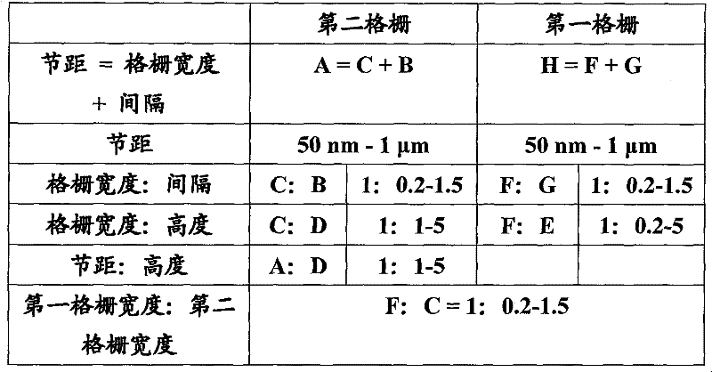
Reference table 1 and Fig. 2, line grid polarizer preferably according to the present invention comprise being arranged in to have first grid layer of particular sections apart from least one first grid 110 of H, width F and height E comprising on the base material 100; Have second grid layer of particular sections comprising on first grid 110 with being formed on apart from least one second grid 112 of A, width C and height D.Especially, preferred first grid 110 and second grid 112 ratio that forms the width F that makes first grid 110 and the width C of second grid 112 satisfies F: C=1: (0.2 to 1.5).
In addition; Second grid 112 is processed by metal material; And can form and make the width C of second grid and the ratio of the interval B between second grid satisfy C: B=1: (0.2 to 1.5); The width C of second grid satisfies C: D=1 with the ratio of the height D of second grid: (1 to 5), perhaps the pitch A of second grid satisfies A: D=1 with the ratio of the height D of second grid: (1 to 5).Said structure can make transmissivity, brightness and polarization efficiency maximization.In this case, the pitch A of preferred second grid 112 is 50nm to 1 μ m.
Especially, hereinafter with reference Fig. 3 describes the measurement result that transmissivity improves degree, wherein only considers the pitch A of second grid 112 and the ratio of the height D of second grid.
Fig. 3 shows that the ratio as the pitch A of second grid in a preferred embodiment of the present invention and the height D of second grid satisfies A: D=1: the measurement result when (1 to 5).
The height D that Fig. 3 (a) is presented at second grid 112 be 100 to 150nm and the pitch A of second grid 112 be under 100 to 200nm the situation, the transmissivity that reduces along with the width C of second grid 112.
In addition, the height D that Fig. 3 (b) is presented at second grid 112 be 151 to 200nm and the pitch A of second grid 112 be under 100 to 200nm the situation, the transmissivity that reduces along with the width C of second grid 112.
In addition, the height D that Fig. 3 (c) is presented at second grid 112 be 201 to 300nm and the pitch A of second grid 112 be under 100 to 200nm the situation, the transmissivity that reduces along with the width C of second grid 112.That is to say, visible from Fig. 3 (a), 3 (b) and 3 (c), when the height D of second grid 112 at A: D=1: in the scope of (1 to 5) when constant transmissivity reduce gradually with the width C of grid 112 and increase.
For example, Fig. 4 shows when transmissivity is 40 to 60%, preferred high brightness 50% time.Correspondingly, can find out,, then can obtain high-transmission rate if first and second grids 110 and 112 form and have above-mentioned height E and D and above-mentioned width F and C or second grid 112 and form and have above-mentioned pitch A.
In addition, table 2 shows transmissivity and the polarization efficiency of the pitch A of second grid 112 according to the present invention.nm
Table 2
| The pitch of second grid (A) | 100nm | 120nm | 150nm | 200nm | 250nm |
| Transmissivity (%) | 57.66 | 57.42 | 56.60 | 52.4 | 66.9 |
| Polarization efficiency | 99.9933 | 99.9853 | 99.9733 | 99.7735 | 99.279 |
Maximum optical effect can realize according to the structure of first grid of the present invention and according to the structure of second grid of the present invention through control.For this reason; Especially; First grid 110 according to the present invention is processed by polymeric material; And be preferably formed to the width F that makes the grid of winning and the ratio of the interval G between first grid and satisfy F: G=1: (0.2 to 1.5), perhaps the width F of first grid satisfies F: E=1 with the ratio of the height E of first grid: (0.2 to 5).In addition, first grid according to the present invention can form the pitch H with 50nm to 1 μ m.
First grid and second grid can form and have various ways according to the present invention, for example bar, curve, quadrilateral and triangle.That is to say that the horizontal xsect separately of first and second grids can have various ways, for example circle, ellipse or polygon.
Method according to manufacturing line grid polarizer of the present invention is described with reference to figure 5 to 7 hereinafter.Fig. 5 to 7 shows the method according to manufacturing line grid polarizer of the present invention.In this embodiment, having described wherein, first grid and second grid form the instance with strip separately.
Method according to manufacturing line grid polarizer of the present invention comprises first step: the first grid basal layer 122 that is stacked on the base material 100 through processing forms a plurality of first grids 110, and each all has the particular sections distance said a plurality of first grids 110; Second step: on said first grid, form the second grid basal layer 124; And third step: form a plurality of second grids 112 through the etching second grid basal layer 124.
Especially, in this case, the width F of preferred first grid satisfies F: C=1 with the ratio of the width of the second grid C: (0.2 to 1.5).
With reference to figure 5, at first, in the first step of manufacturing method according to the invention, the first grid basal layer 122 forms through polymeric material (for example UV resin) is coated on the base material 100.The impressing mould 120 that next, will have groove 126 and a teat 128 scribbles above that on the base material 100 of the first grid basal layer 122 and aims at.In this article, a plurality of grooves 126 of impressing mould 120 are spaced apart from each other with specific interval and repeat and form, and a plurality of teats 128 of impressing mould 120 are spaced apart from each other with specific interval and repeat and form.In addition, the groove 126 of impressing mould 120 is corresponding with each position that wherein forms first grid 110 respectively.
In this case, the height of each groove 126 of impressing mould 120 is corresponding with height E with the width F of first grid with width.Preferably, the height and the width of the groove 126 of impressing mould 120 satisfy F: E=1: (0.2 to 5) (promptly according to the height E of first grid of the present invention and ratio of the width F of first grid).
That is to say; Utilizing impressing mould to form under the situation of first grid; Preferably; In the structure (being the result of impressing mould) of first grid, impression groove and highly may be controlled to the width F that makes the grid of winning and the ratio of the interval G between first grid satisfies F: G=1: (0.2 to 1.5), perhaps the width F of first grid satisfies F: E=1 with the ratio of the height E of first grid: (0.2 to 5).
In addition, the groove 126 of impressing mould 120 forms strip.Polymeric material 122 pressurizations to forming the first grid basal layer make it contact with the groove 126 of impressing mould 120 and also stand the UV radiation subsequently.Correspondingly, a plurality of first grids 110 are formed in the groove 126 corresponding parts of polymeric material wherein 122 and impressing mould 120.
Next, as shown in Figure 6, the second grid basal layer 124 (being metal level) is deposited on the base material 100 that wherein forms a plurality of first grids 110.As shown in Figure 7, the etching second grid basal layer 124 is to form second grid 112 on first grid 110.
More specifically, on the second grid basal layer 124 (being metal level) that is deposited on the base material 100 (wherein forming a plurality of first grids 110), carry out the Wet-type etching process, form second grid 112 thus.
In addition; Preferably; Carry out Wet-type etching; Make the width C of second grid and the ratio of the interval B between second grid satisfy C: B=1: (0.2 to 1.5), the width C of second grid satisfies C: D=1 with the ratio of the height D of second grid: (1 to 5), perhaps the pitch A of second grid satisfies A: D=1 with the ratio of the height D of second grid: (1 to 5).Correspondingly, accomplishing wherein, second grid 112 is respectively formed at the line grid polarizer on first grid 110 on the base material 100.
Described like preceding text about Fig. 5 to 7, comprise that the line grid polarizer of first and second grids 110 and 112 can only utilize moulding process, deposition process and Wet-type etching process to make.Because the manufacturing approach step can reduce as described above, so can reduce manufacturing cost and can produce in enormous quantities.
On the other hand, Fig. 8 is that first grid 140 that shows its center line grid polarizer has radius curve but not the viewgraph of cross-section of the instance of strip.Fig. 9 to 11 is figure that the method for the manufacturing line grid polarizer that shows among Fig. 8 is shown.Identical in the process that shows among Fig. 9 to 11 and structure and Fig. 2 and 5 to 7, and omit its explanation.Yet; The outside surface of the horizontal xsect of first grid with semicircle or half elliptic and first grid has under the situation of curved surface therein, and the perpendicular line that the horizontal point of the point that the width F of first grid and the interval G between first grid are in contact with one another based on the curved surface from the half height E of first grid and first grid is drawn downwards limits.
In addition, as in the structure that shows among Figure 12, first grid 110 can have strip, and the xsect of second grid can have circle or ellipse.Line grid polarizer for example shows among Figure 12, can form first grid 110 and the second grid basal layer through order and control the Wet-type etching process then and implement.
Figure 13 shows another embodiment of the present invention.The width F of first grid and the width C of second grid satisfy F in the preferred embodiment of the present invention therein: C=1: under the situation of (0.2 to 1.5), the width C of second grid can be wideer, shown in figure 13 than the width F of first grid.That is to say that Figure 13 shows that wherein the width C of second grid is 1 to 1.5 times the structure of the width F of first grid.In this case, the outside surface of second grid can have oval curved surface, strip or quadrangle form.
Figure 14 shows to comprise the viewgraph of cross-section according to the liquid-crystal apparatus of line grid polarizer of the present invention.
With reference to Figure 14, liquid-crystal apparatus according to an embodiment of the invention comprises LCD panel 200, is used for providing to LCD panel 200 back light unit 230 and the line grid polarizer of light.Line grid polarizer is patterned on the top or bottom of LCD panel 200, or on arbitrary surface of the optical sheet that in back light unit 230, comprises.The reflector plate 234 that back light unit 230 comprises light source 232, is configured to spread the diffusion sheet 236 of the light that is produced by light source 232 and places light source 232 belows.
The photoconduction that diffusion sheet 236 will receive from light source 232 is to the place ahead of LCD panel 200, and in wide region, to have equally distributed mode diffusion light, makes illumination be mapped to LCD panel 200.The preferred use by the two sides all is coated with film that the transparent resin of the member that is useful on the light diffusion processes as diffusion sheet 236.
Comprise the black matix, the color filter that is configured to realize color that are configured to prevent light and reveal, be configured to be formed on the last base material of color filter base material 212 along the color filter array that pixel electrode forms the public electrode of vertical electric field and is coated in the last alignment films that is used to make liquid crystal aligning on the electrode.In addition, comprise form the gate line that intersects each other with data line, separately be formed on thin film transistor (TFT), the pixel electrode that is connected with thin film transistor (TFT) at gate line and data line joining place and be coated in pixel electrode and thin film transistor (TFT) on be used to make the thin film transistor (TFT) array of the following alignment films of liquid crystal aligning to be formed on the following base material of thin film transistor (TFT) base material 210.
Although combined the embodiment of the present invention shown in the accompanying drawing to describe the present invention, it is not limited thereto.Those skilled in the art obviously knows, can carry out multiplely substituting, revising and change to it, and not depart from the scope of the present invention and spirit.
Shown in figure 14, line grid polarizer according to the present invention can be formed on the below of LCD panel 200, perhaps can be formed on the top of LCD panel 200, on arbitrary surface of the optical sheet that perhaps in back light unit 230, comprises.
In addition, line grid polarizer according to the present invention can be attached to the surface of Liquid Crystal Module, and is as shown in the figure.A plurality of line grid polarizers can be with certain separation.And second grid can face upward or downward orientation.
In addition, line grid polarizer according to the present invention comprises second grid 112 that is arranged in first grid 110 on the bottom of LCD panel 200 and on first grid 110, forms with specific interval.
Except above-mentioned liquid-crystal apparatus, line grid polarizer according to the present invention can be applicable to realize the display device of 3D stereo-picture.Correspondingly, line grid polarizer according to the present invention can be widely used in and implement high brightness and realize high reliability.
Claims (17)
Applications Claiming Priority (3)
| Application Number | Priority Date | Filing Date | Title |
|---|---|---|---|
| KR10-2009-0031463 | 2009-04-10 | ||
| KR1020090031463A KR101610376B1 (en) | 2009-04-10 | 2009-04-10 | A wire grid polarizer, liquid crystal display including the same and method of manufacturing the wire grid polarizer |
| PCT/KR2010/002236 WO2010117249A2 (en) | 2009-04-10 | 2010-04-12 | Wire grid polarizer, lcd device including the same, 3d stereoscopic image display device, and manufacturing method of wire grid polarizer |
Publications (1)
| Publication Number | Publication Date |
|---|---|
| CN102549482A true CN102549482A (en) | 2012-07-04 |
Family
ID=42936752
Family Applications (1)
| Application Number | Title | Priority Date | Filing Date |
|---|---|---|---|
| CN2010800162627A Pending CN102549482A (en) | 2009-04-10 | 2010-04-12 | Wire grid polarizer, LCD device including the same, 3D stereoscopic image display device, and manufacturing method of wire grid polarizer |
Country Status (5)
| Country | Link |
|---|---|
| US (1) | US9599762B2 (en) |
| JP (1) | JP2012523582A (en) |
| KR (1) | KR101610376B1 (en) |
| CN (1) | CN102549482A (en) |
| WO (1) | WO2010117249A2 (en) |
Cited By (8)
| Publication number | Priority date | Publication date | Assignee | Title |
|---|---|---|---|---|
| CN105074554A (en) * | 2013-01-03 | 2015-11-18 | 英派尔科技开发有限公司 | Display devices including inorganic components and methods of making and using the same |
| CN107167863A (en) * | 2017-07-07 | 2017-09-15 | 深圳市华星光电技术有限公司 | The preparation method of nanometer wiregrating polaroid |
| CN109471289A (en) * | 2017-09-07 | 2019-03-15 | 三星Sdi株式会社 | Polarizer and optical display including the same |
| CN110927721A (en) * | 2018-08-31 | 2020-03-27 | 麦格纳覆盖件有限公司 | Automotive radar/lidar behind a reflective surface |
| US10802189B2 (en) | 2017-09-22 | 2020-10-13 | Au Optronics Corporation | Wire grid polarizer and display panel using the same |
| WO2022001449A1 (en) * | 2020-06-29 | 2022-01-06 | 京东方科技集团股份有限公司 | Metal wire grid polarizer and manufacturing method therefor, and display device |
| WO2022001447A1 (en) * | 2020-06-30 | 2022-01-06 | 京东方科技集团股份有限公司 | Wire grid polarizer and fabrication method therefor |
| CN116053288A (en) * | 2023-01-28 | 2023-05-02 | 合肥晶合集成电路股份有限公司 | Image sensor and manufacturing method thereof |
Families Citing this family (26)
| Publication number | Priority date | Publication date | Assignee | Title |
|---|---|---|---|---|
| CN102834749B (en) * | 2010-03-30 | 2015-02-04 | 日本电气株式会社 | Optical element, light source device, and projection display device |
| KR20130118729A (en) * | 2010-04-27 | 2013-10-30 | 더 리젠츠 오브 더 유니버시티 오브 미시건 | Display device having plasmonic color filters and photovoltaic capabilities |
| KR20120032776A (en) * | 2010-09-29 | 2012-04-06 | 엘지이노텍 주식회사 | A wire grid polarizer and backlightounit uaing the same |
| KR101319444B1 (en) * | 2010-10-20 | 2013-10-17 | 엘지이노텍 주식회사 | Liquid Crystal Display within a wire grid polarazer |
| US20150077851A1 (en) * | 2010-12-30 | 2015-03-19 | Moxtek, Inc. | Multi-layer absorptive wire grid polarizer |
| US8552439B2 (en) * | 2011-04-07 | 2013-10-08 | Himax Display, Inc. | Light-emitting diode package |
| EP2699952A4 (en) | 2011-04-20 | 2015-06-24 | Univ Michigan | SPECTRAL FILTERING FOR VISUAL DISPLAYS AND IMAGING SYSTEM HAVING MINIMUM ANGULAR DEPENDENCY |
| KR101775163B1 (en) * | 2011-07-28 | 2017-09-05 | 엘지이노텍 주식회사 | Manufacturing method of mold for nano imprint and mold for nano imprint by using the same |
| FR2994602B1 (en) * | 2012-08-16 | 2014-09-12 | Commissariat Energie Atomique | SPECTRAL FILTERING DEVICE IN VISIBLE AND INFRARED DOMAINS |
| KR20140030382A (en) | 2012-08-27 | 2014-03-12 | 삼성디스플레이 주식회사 | Liquid crystal display and fabrication method of the same |
| US9547107B2 (en) | 2013-03-15 | 2017-01-17 | The Regents Of The University Of Michigan | Dye and pigment-free structural colors and angle-insensitive spectrum filters |
| AU2013100685B4 (en) * | 2013-05-21 | 2013-09-12 | Innovia Security Pty Ltd | Optical device including vertical pixels |
| JP5929860B2 (en) | 2013-09-24 | 2016-06-08 | ウシオ電機株式会社 | Grid polarizing element manufacturing method |
| WO2015060943A1 (en) * | 2013-10-24 | 2015-04-30 | Moxtek, Inc. | Polarizer with variable inter-wire distance |
| US9354374B2 (en) * | 2013-10-24 | 2016-05-31 | Moxtek, Inc. | Polarizer with wire pair over rib |
| US10447040B2 (en) | 2014-10-15 | 2019-10-15 | Cummins Power Generation Ip, Inc. | Programmable inverter for controllable grid response |
| KR20160049162A (en) * | 2014-10-24 | 2016-05-09 | 삼성디스플레이 주식회사 | A method of manufacturing a mold and a method of manufacturing a polarizer |
| KR20170062590A (en) * | 2015-11-27 | 2017-06-08 | 삼성디스플레이 주식회사 | Wire grid polarizer plate and method for manufacturing the smae |
| KR102567008B1 (en) * | 2016-03-18 | 2023-08-14 | 삼성디스플레이 주식회사 | Display devic including wire grid polarizer and manufacturing method thereof |
| JP6720625B2 (en) * | 2016-03-25 | 2020-07-08 | 大日本印刷株式会社 | Polarizer and method for manufacturing polarizer |
| JP6230689B1 (en) * | 2016-12-28 | 2017-11-15 | デクセリアルズ株式会社 | Polarizing plate, method for producing the same, and optical instrument |
| JP7226936B2 (en) * | 2018-07-26 | 2023-02-21 | デクセリアルズ株式会社 | Polarizing plate and optical equipment |
| US20200041807A1 (en) * | 2018-08-02 | 2020-02-06 | Christie Digital Systems Usa, Inc. | Light emitting diode display with a monolithic wire-grid polarizer for producing three-dimensional images |
| CN109031507B (en) * | 2018-08-15 | 2020-01-24 | 京东方科技集团股份有限公司 | Light guide plate and its manufacturing method, backlight module and display device |
| PH12020050192B1 (en) * | 2019-07-17 | 2023-12-01 | Moxtek Inc | Reflective wire grid polarizer with transparent cap |
| KR102703701B1 (en) * | 2021-11-02 | 2024-09-05 | 한국과학기술원 | Nickel stamp and Method of manufacturing the same |
Citations (6)
| Publication number | Priority date | Publication date | Assignee | Title |
|---|---|---|---|---|
| CN1497273A (en) * | 2002-10-15 | 2004-05-19 | 伊斯曼柯达公司 | Wiregrating polarizer |
| CN1520524A (en) * | 2001-04-26 | 2004-08-11 | 日本板硝子株式会社 | Polarizing element and manufacturing method thereof |
| CN1952700A (en) * | 2005-10-17 | 2007-04-25 | 旭化成株式会社 | Wire grid polarizer and manufacturing method of the same |
| CN101080656A (en) * | 2004-12-16 | 2007-11-28 | 东丽株式会社 | Polarizing plate, method of producing the polarizing plate, and liquid crystal display device using the polarizing plate |
| US20080094547A1 (en) * | 2006-10-20 | 2008-04-24 | Tatsuya Sugita | Wire grid polarized and liquid crystal display device using the same |
| US20080278811A1 (en) * | 2004-12-06 | 2008-11-13 | Perkins Raymond T | Selectively Absorptive Wire-Grid Polarizer |
Family Cites Families (22)
| Publication number | Priority date | Publication date | Assignee | Title |
|---|---|---|---|---|
| US3293331A (en) * | 1962-11-13 | 1966-12-20 | Little Inc A | Method of forming replicas of contoured substrates |
| CN100592112C (en) * | 2002-02-12 | 2010-02-24 | 奥尔利康贸易股份公司(特吕巴赫) | Component comprising sub-micron hollow spaces |
| TWI256491B (en) * | 2004-07-27 | 2006-06-11 | Pavonine Inc | Liquid crystal display device having thin polarizing film and thin phase retardation film |
| KR100483352B1 (en) * | 2004-07-27 | 2005-04-14 | (주)파버나인 | Liquid crystal display device using thin film polarizers and retarders |
| JP4442760B2 (en) * | 2004-08-06 | 2010-03-31 | 旭化成イーマテリアルズ株式会社 | Inorganic material selective pattern forming method and grid-type polarizing element |
| US20060056024A1 (en) * | 2004-09-15 | 2006-03-16 | Ahn Seh W | Wire grid polarizer and manufacturing method thereof |
| US7570424B2 (en) * | 2004-12-06 | 2009-08-04 | Moxtek, Inc. | Multilayer wire-grid polarizer |
| KR100656999B1 (en) * | 2005-01-19 | 2006-12-13 | 엘지전자 주식회사 | Method of manufacturing mold for manufacturing lattice of line lattice polarizing film and line lattice polarizing film |
| KR20090006066A (en) | 2006-04-07 | 2009-01-14 | 아사히 가라스 가부시키가이샤 | Wire grid polarizer and its manufacturing method |
| WO2008022099A2 (en) * | 2006-08-15 | 2008-02-21 | Api Nanofabrication And Research Corp. | Polarizer films and methods of making the same |
| US8755113B2 (en) * | 2006-08-31 | 2014-06-17 | Moxtek, Inc. | Durable, inorganic, absorptive, ultra-violet, grid polarizer |
| JP4520445B2 (en) * | 2006-10-11 | 2010-08-04 | 旭化成イーマテリアルズ株式会社 | Wire grid polarizer |
| JP2008181113A (en) * | 2006-12-27 | 2008-08-07 | Toray Ind Inc | Reflection type polarizer and liquid crystal display device |
| US8027086B2 (en) * | 2007-04-10 | 2011-09-27 | The Regents Of The University Of Michigan | Roll to roll nanoimprint lithography |
| JP5069036B2 (en) * | 2007-04-16 | 2012-11-07 | 旭化成イーマテリアルズ株式会社 | Polarizing plate with high degree of polarization |
| KR100922186B1 (en) | 2007-06-18 | 2009-10-19 | 미래나노텍(주) | Method of manufacturing wire grid polarizer |
| KR100980284B1 (en) | 2007-09-07 | 2010-09-06 | 미래나노텍(주) | Nanowire grid polarizer with improved adhesion and manufacturing method |
| JP2009075265A (en) * | 2007-09-19 | 2009-04-09 | Nippon Zeon Co Ltd | Manufacturing method of grid polarizing film |
| KR101457254B1 (en) | 2007-09-28 | 2014-10-31 | 아사히 가라스 가부시키가이샤 | Photocurable composition, method for producing fine patterned body, and optical device |
| JP5206029B2 (en) | 2008-03-04 | 2013-06-12 | ソニー株式会社 | Liquid crystal display |
| KR100952137B1 (en) | 2008-04-18 | 2010-04-09 | 실리콘 디스플레이 (주) | Stereoscopic image display device and manufacturing method thereof |
| KR20110031440A (en) | 2008-07-10 | 2011-03-28 | 아사히 가라스 가부시키가이샤 | Wire grid polarizer and its manufacturing method |
-
2009
- 2009-04-10 KR KR1020090031463A patent/KR101610376B1/en not_active Expired - Fee Related
-
2010
- 2010-04-12 JP JP2012504626A patent/JP2012523582A/en active Pending
- 2010-04-12 CN CN2010800162627A patent/CN102549482A/en active Pending
- 2010-04-12 US US13/263,814 patent/US9599762B2/en not_active Expired - Fee Related
- 2010-04-12 WO PCT/KR2010/002236 patent/WO2010117249A2/en not_active Ceased
Patent Citations (6)
| Publication number | Priority date | Publication date | Assignee | Title |
|---|---|---|---|---|
| CN1520524A (en) * | 2001-04-26 | 2004-08-11 | 日本板硝子株式会社 | Polarizing element and manufacturing method thereof |
| CN1497273A (en) * | 2002-10-15 | 2004-05-19 | 伊斯曼柯达公司 | Wiregrating polarizer |
| US20080278811A1 (en) * | 2004-12-06 | 2008-11-13 | Perkins Raymond T | Selectively Absorptive Wire-Grid Polarizer |
| CN101080656A (en) * | 2004-12-16 | 2007-11-28 | 东丽株式会社 | Polarizing plate, method of producing the polarizing plate, and liquid crystal display device using the polarizing plate |
| CN1952700A (en) * | 2005-10-17 | 2007-04-25 | 旭化成株式会社 | Wire grid polarizer and manufacturing method of the same |
| US20080094547A1 (en) * | 2006-10-20 | 2008-04-24 | Tatsuya Sugita | Wire grid polarized and liquid crystal display device using the same |
Cited By (15)
| Publication number | Priority date | Publication date | Assignee | Title |
|---|---|---|---|---|
| US9261730B2 (en) | 2013-01-03 | 2016-02-16 | Empire Technology Development Llc | Display devices including inorganic components and methods of making and using the same |
| CN105074554B (en) * | 2013-01-03 | 2018-04-17 | 英派尔科技开发有限公司 | Display device including inorganic component and preparation method thereof and application method |
| CN105074554A (en) * | 2013-01-03 | 2015-11-18 | 英派尔科技开发有限公司 | Display devices including inorganic components and methods of making and using the same |
| CN107167863A (en) * | 2017-07-07 | 2017-09-15 | 深圳市华星光电技术有限公司 | The preparation method of nanometer wiregrating polaroid |
| CN107167863B (en) * | 2017-07-07 | 2019-09-10 | 深圳市华星光电技术有限公司 | The production method of nanometer wiregrating polaroid |
| CN109471289B (en) * | 2017-09-07 | 2021-10-22 | 三星Sdi株式会社 | Polarizing plate and optical display including the same |
| CN109471289A (en) * | 2017-09-07 | 2019-03-15 | 三星Sdi株式会社 | Polarizer and optical display including the same |
| US10802189B2 (en) | 2017-09-22 | 2020-10-13 | Au Optronics Corporation | Wire grid polarizer and display panel using the same |
| CN110927721A (en) * | 2018-08-31 | 2020-03-27 | 麦格纳覆盖件有限公司 | Automotive radar/lidar behind a reflective surface |
| US12235389B2 (en) | 2018-08-31 | 2025-02-25 | Magna Electronics Inc. | Automotive radar / LIDAR behind reflective surfaces |
| WO2022001449A1 (en) * | 2020-06-29 | 2022-01-06 | 京东方科技集团股份有限公司 | Metal wire grid polarizer and manufacturing method therefor, and display device |
| CN113933924A (en) * | 2020-06-29 | 2022-01-14 | 京东方科技集团股份有限公司 | Wire grid polarizer, method for making the same, and display device |
| WO2022001447A1 (en) * | 2020-06-30 | 2022-01-06 | 京东方科技集团股份有限公司 | Wire grid polarizer and fabrication method therefor |
| US12248247B2 (en) | 2020-06-30 | 2025-03-11 | Boe Technology Group Co., Ltd. | Wire grid polarizer and fabrication method therefor |
| CN116053288A (en) * | 2023-01-28 | 2023-05-02 | 合肥晶合集成电路股份有限公司 | Image sensor and manufacturing method thereof |
Also Published As
| Publication number | Publication date |
|---|---|
| US9599762B2 (en) | 2017-03-21 |
| US20120086887A1 (en) | 2012-04-12 |
| KR101610376B1 (en) | 2016-04-08 |
| JP2012523582A (en) | 2012-10-04 |
| WO2010117249A2 (en) | 2010-10-14 |
| KR20100112926A (en) | 2010-10-20 |
| WO2010117249A3 (en) | 2011-01-20 |
Similar Documents
| Publication | Publication Date | Title |
|---|---|---|
| CN102549482A (en) | Wire grid polarizer, LCD device including the same, 3D stereoscopic image display device, and manufacturing method of wire grid polarizer | |
| CN105549236B (en) | Switchable peep-proof device, preparation method thereof and display device | |
| EP2523038B1 (en) | Color filter substrate capable of polarizing and manufacturing method thereof | |
| US11237429B2 (en) | Light guiding assembly and fabricating method thereof, backlight module and display device | |
| KR101336097B1 (en) | Liquid crystal display device having Wire grid polarizer | |
| JP2024138322A5 (en) | ||
| JP2006201782A (en) | Wire grid polarizing film, method for manufacturing polarizing film, liquid crystal display using the same, and method for manufacturing mold for manufacturing grid of wire grid polarizing film | |
| US9703027B2 (en) | Wire grid polarizer, liquid crystal display having the same and method of manufacturing the same | |
| KR102248876B1 (en) | Array substrate for display device and displya device | |
| CN105137665A (en) | Display substrate, preparation method thereof, and display device | |
| CN107219685A (en) | The display methods of display device and display device | |
| WO2015096256A1 (en) | Fan-out area structure of narrow-frame liquid crystal display | |
| KR20120032776A (en) | A wire grid polarizer and backlightounit uaing the same | |
| TW201921041A (en) | Light guides including gratings | |
| CN100510859C (en) | Reflective display and method of producing same | |
| KR101714035B1 (en) | A wire grid polarizer, liquid crystal display, 3d-display including the same and method of manufacturing the wire grid polarizer | |
| KR20140064526A (en) | Display panel having improved light-use efficiency, dispaly apparatus including the display panel, and method of fabricating the display panel | |
| CN105700056A (en) | Polarizing plate, TFT substrate including the polarizing plate, and method of manufacturing the polarizing plate | |
| US9594206B2 (en) | Complex substrate for display apparatus, display apparatus having the same and method of manufacturing the same | |
| CN107884985A (en) | Liquid crystal display device | |
| US8009243B2 (en) | Light diffusion device, backlight module and liquid crystal display | |
| CN105652510A (en) | Display panel and manufacture method thereof as well as display device | |
| JP5549087B2 (en) | Manufacturing method of optical sheet | |
| KR20130065377A (en) | Liquid crystal display device and method of fabricating the same | |
| CN110703494A (en) | Backlight module and display device |
Legal Events
| Date | Code | Title | Description |
|---|---|---|---|
| C06 | Publication | ||
| PB01 | Publication | ||
| C10 | Entry into substantive examination | ||
| SE01 | Entry into force of request for substantive examination | ||
| C12 | Rejection of a patent application after its publication | ||
| RJ01 | Rejection of invention patent application after publication |
Application publication date: 20120704 |