KR101535224B1 - Duty control circuit and semiconductor device having the same - Google Patents
Duty control circuit and semiconductor device having the same Download PDFInfo
- Publication number
- KR101535224B1 KR101535224B1 KR1020080092944A KR20080092944A KR101535224B1 KR 101535224 B1 KR101535224 B1 KR 101535224B1 KR 1020080092944 A KR1020080092944 A KR 1020080092944A KR 20080092944 A KR20080092944 A KR 20080092944A KR 101535224 B1 KR101535224 B1 KR 101535224B1
- Authority
- KR
- South Korea
- Prior art keywords
- voltage
- node
- duty
- level
- clock signal
- Prior art date
Links
- 239000004065 semiconductor Substances 0.000 title claims abstract description 19
- 230000004044 response Effects 0.000 claims abstract description 52
- 230000000630 rising effect Effects 0.000 claims description 24
- 230000007704 transition Effects 0.000 claims description 17
- 238000000034 method Methods 0.000 claims description 8
- 230000003139 buffering effect Effects 0.000 claims description 2
- 230000007274 generation of a signal involved in cell-cell signaling Effects 0.000 claims description 2
- 102100040862 Dual specificity protein kinase CLK1 Human genes 0.000 description 31
- 101000749294 Homo sapiens Dual specificity protein kinase CLK1 Proteins 0.000 description 31
- 102100040844 Dual specificity protein kinase CLK2 Human genes 0.000 description 25
- 101000749291 Homo sapiens Dual specificity protein kinase CLK2 Proteins 0.000 description 25
- 238000010586 diagram Methods 0.000 description 16
- 239000000872 buffer Substances 0.000 description 12
- 230000007423 decrease Effects 0.000 description 11
- 238000001514 detection method Methods 0.000 description 4
- 230000003247 decreasing effect Effects 0.000 description 3
- 230000008859 change Effects 0.000 description 2
- 230000008878 coupling Effects 0.000 description 2
- 238000010168 coupling process Methods 0.000 description 2
- 238000005859 coupling reaction Methods 0.000 description 2
- 101100113692 Caenorhabditis elegans clk-2 gene Proteins 0.000 description 1
- 230000003111 delayed effect Effects 0.000 description 1
- 230000007257 malfunction Effects 0.000 description 1
- 230000004048 modification Effects 0.000 description 1
- 238000012986 modification Methods 0.000 description 1
Images


Classifications
-
- G—PHYSICS
- G11—INFORMATION STORAGE
- G11C—STATIC STORES
- G11C5/00—Details of stores covered by group G11C11/00
- G11C5/14—Power supply arrangements, e.g. power down, chip selection or deselection, layout of wirings or power grids, or multiple supply levels
-
- H—ELECTRICITY
- H03—ELECTRONIC CIRCUITRY
- H03K—PULSE TECHNIQUE
- H03K5/00—Manipulating of pulses not covered by one of the other main groups of this subclass
- H03K5/156—Arrangements in which a continuous pulse train is transformed into a train having a desired pattern
- H03K5/1565—Arrangements in which a continuous pulse train is transformed into a train having a desired pattern the output pulses having a constant duty cycle
-
- G—PHYSICS
- G11—INFORMATION STORAGE
- G11C—STATIC STORES
- G11C7/00—Arrangements for writing information into, or reading information out from, a digital store
- G11C7/22—Read-write [R-W] timing or clocking circuits; Read-write [R-W] control signal generators or management
-
- H—ELECTRICITY
- H03—ELECTRONIC CIRCUITRY
- H03K—PULSE TECHNIQUE
- H03K5/00—Manipulating of pulses not covered by one of the other main groups of this subclass
- H03K2005/00013—Delay, i.e. output pulse is delayed after input pulse and pulse length of output pulse is dependent on pulse length of input pulse
- H03K2005/00019—Variable delay
- H03K2005/00058—Variable delay controlled by a digital setting
Landscapes
- Physics & Mathematics (AREA)
- Nonlinear Science (AREA)
- Engineering & Computer Science (AREA)
- Power Engineering (AREA)
- Dram (AREA)
- Logic Circuits (AREA)
Abstract
프로그래머블(programmable)한 듀티 제어특성을 갖는 듀티 제어회로 및 이를 구비하는 반도체 장치가 개시된다. 본 발명의 일예에 따른 상기 듀티 제어회로는, 제1 노드를 통해 제공되는 입력 클록신호를 수신하고, 상기 입력 클록신호에 응답하여 제2 노드의 전압을 제1 레벨 또는 제2 레벨로 변동시키는 클록 입력부 및 상기 제1 레벨의 전압 또는 상기 제2 레벨의 전압에 각각 연결되는 복수의 스위치들을 포함하고, 상기 복수의 스위치들 각각으로 제공되는 제어신호에 응답하여 상기 제1 레벨의 전압 또는 상기 제2 레벨의 전압을 상기 제2 노드로 전달하는 슬루(slew) 제어부를 구비하는 것을 특징으로 한다.A duty control circuit having a programmable duty control characteristic and a semiconductor device having the duty control circuit are disclosed. The duty control circuit according to an exemplary embodiment of the present invention includes a duty control circuit that receives an input clock signal provided through a first node and generates a clock signal that varies a voltage of a second node to a first level or a second level in response to the input clock signal, And a plurality of switches respectively connected to the input unit and the voltage of the first level or to the voltage of the second level, wherein in response to the control signal provided to each of the plurality of switches, Level voltage to the second node when the voltage of the first node is higher than the voltage of the second node.
Description
본 발명은 듀티 제어회로 및 이를 구비하는 반도체 장치에 관한 것으로서, 자세하게는 프로그래머블(programmable)한 듀티 제어특성을 갖는 듀티 제어회로 및 이를 구비하는 반도체 장치에 관한 것이다.BACKGROUND OF THE
듀티 제어회로는 입력되는 클록신호의 듀티를 조절하여 출력 클록신호가 원하는 듀티를 갖도록 제어하기 위한 회로로서 반도체 장치에 일반적으로 구비된다. 반도체 장치가 고속화됨에 따라 클록신호의 듀티를 정밀하게 조절하는 것이 중요하며, 또한 클록신호의 듀티를 프로그래머블하게 조절하는 것이 중요하다. 일예로서, 반도체 장치가 DDR(Double Data Rate) SDRAM인 경우 클록 신호의 상승 에지(rising edge) 및 하강 에지(falling edge)를 모두 이용하여 동작하므로, 듀티 제어회로의 출력 클록신호에 듀티 왜곡이 발생하게 되면 반도체 장치의 오동작을 유발할 수 있다. The duty control circuit is generally provided in a semiconductor device as a circuit for controlling the duty of an input clock signal so that the output clock signal has a desired duty. As the semiconductor device speeds up, it is important to precisely control the duty of the clock signal, and it is also important to programmably adjust the duty of the clock signal. For example, when the semiconductor device is a double data rate (DDR) SDRAM, the semiconductor memory device operates using both a rising edge and a falling edge of a clock signal. As a result, a duty distortion occurs in the output clock signal of the duty control circuit , Malfunction of the semiconductor device may be caused.
일반적으로, 클록 신호의 듀티를 제어하기 위한 회로로서, 버퍼의 딜레이를 이용하여 듀티를 조절하는 방식이 사용되고 있다. 즉, 입력 클록신호와 상기 입력 클록신호를 지연한 신호에 대해 논리 연산을 수행함으로써 출력 클록신호의 듀티를 조절한다. 그러나, 이와 같은 종래의 방식에서는 버퍼의 딜레이 양에 의해 듀티가 제어되므로, 버퍼의 딜레이 양이 커지게 되면 듀티를 정밀하게 조절하기 어렵다. 또한 듀티의 조절이 프로그래머블하게 하기 위해서는 멀티플렉서 등의 별도의 회로가 필요하나, 상기와 같은 멀티플렉서에 의한 방식은 듀티의 조절을 다양하게 프로그램할 수 없는 단점이 있다. Generally, as a circuit for controlling the duty of a clock signal, a method of adjusting the duty by using the delay of the buffer is used. That is, the duty of the output clock signal is adjusted by performing a logical operation on the input clock signal and the signal delayed from the input clock signal. However, in such a conventional system, the duty is controlled by the amount of delay of the buffer, so that it is difficult to precisely control the duty as the amount of delay of the buffer becomes large. Further, in order to make the control of the duty programmable, a separate circuit such as a multiplexer is required. However, the method using the multiplexer has a disadvantage in that it is not possible to program variously the duty control.
본 발명은 상기와 같은 문제점을 해결하기 위한 것으로서, 듀티 제어의 정밀성 및 프로그래머블 특성을 개선한 듀티 제어회로 및 이를 구비하는 반도체 장치를 제공하는 것을 목적으로 한다.SUMMARY OF THE INVENTION It is an object of the present invention to provide a duty control circuit and a semiconductor device including the duty control circuit, which improve the accuracy and programmability of duty control.
상기와 같은 목적을 달성하기 위하여, 본 발명의 일실시예에 따른 듀티 제어회로는, 제1 노드를 통해 제공되는 입력 클록신호를 수신하고, 상기 입력 클록신호에 응답하여 제2 노드의 전압을 제1 레벨 또는 제2 레벨로 변동시키는 클록 입력부 및 상기 제1 레벨의 전압 또는 상기 제2 레벨의 전압에 각각 연결되는 복수의 스위치들을 포함하고, 상기 복수의 스위치들 각각으로 제공되는 제어신호에 응답하여 상기 제1 레벨의 전압 또는 상기 제2 레벨의 전압을 상기 제2 노드로 전달하는 슬루(slew) 제어부를 구비하는 것을 특징으로 한다.According to an aspect of the present invention, there is provided a duty control circuit for receiving an input clock signal provided through a first node and for applying a voltage of a second node in response to the input clock signal, And a plurality of switches respectively connected to the first-level voltage or the second-level voltage, wherein in response to a control signal provided to each of the plurality of switches, And a slew controller for transmitting the voltage of the first level or the voltage of the second level to the second node.
바람직하게는, 상기 클록 입력부는 상기 입력 클록신호를 인버팅하여 출력하는 인버터인 것을 특징으로 한다.Preferably, the clock input unit is an inverter for inverting and outputting the input clock signal.
또한 바람직하게는, 상기 제1 레벨의 전압은 전원전압이며, 상기 제2 레벨의 전압은 접지전압인 것을 특징으로 한다.Preferably, the voltage of the first level is a power supply voltage, and the voltage of the second level is a ground voltage.
한편, 상기 복수의 스위치들은, 상기 제1 레벨의 전압과 상기 제2 노드 사이에 병렬하게 연결되며, 상기 입력 클록신호가 로직 로우로 천이하는 경우 상기 제어신호에 응답하여 선택적으로 턴온됨으로써 상기 제1 레벨의 전압을 상기 제2 노 드로 제공하는 것을 특징으로 한다.The plurality of switches are connected in parallel between the first level voltage and the second node and are selectively turned on in response to the control signal when the input clock signal transits to a logic low, Level voltage to the second node.
바람직하게는, 상기 복수의 스위치들은, 서로 다른 사이즈(size)를 갖는 n 개의 PMOS 트랜지스터를 구비하며(단, n은 정수), 상기 제어신호에 응답하여 선택적으로 턴온됨에 따라 상기 제2 노드의 전압의 라이징 슬루 레이트(rising slew rate)를 조절하는 것을 특징으로 한다.Advantageously, the plurality of switches comprise n PMOS transistors (where n is an integer) having different sizes, and the voltage of the second node as it is selectively turned on in response to the control signal The controller controls the rising slew rate of the antenna.
한편, 상기 복수의 스위치들은, 상기 제2 레벨의 전압과 상기 제2 노드 사이에 병렬하게 연결되며, 상기 입력 클록신호가 로직 하이로 천이하는 경우 상기 제어신호에 응답하여 선택적으로 턴온됨으로써 상기 제2 레벨의 전압을 상기 제2 노드로 제공하는 것을 특징으로 한다.On the other hand, the plurality of switches are connected in parallel between the second level voltage and the second node, and are selectively turned on in response to the control signal when the input clock signal transits to logic high, Level voltage to the second node.
바람직하게는, 상기 복수의 스위치들은, 서로 다른 사이즈(size)를 갖는 n 개의 NMOS 트랜지스터를 구비하며(단, n은 정수), 상기 제어신호에 응답하여 선택적으로 턴온됨에 따라 상기 제2 노드의 전압의 폴링 슬루 레이트(falling slew rate)를 조절하는 것을 특징으로 한다.Advantageously, the plurality of switches comprises n NMOS transistors (where n is an integer) having different sizes, the voltage of the second node as it is selectively turned on in response to the control signal, And controls the falling slew rate of the antenna.
한편, 상기 슬루(slew) 제어부는, 제1 전극이 상기 제1 레벨의 전압에 연결되고, 상기 입력 클록신호에 응답하여 스위칭되는 n 개의 제1 스위치들(단, n은 정수) 및 상기 n 개의 제1 스위치들의 제2 전극과 상기 제2 노드 사이에 각각 연결되며, 대응하는 제어신호에 응답하여 스위칭됨으로써 상기 n 개의 제1 스위치들의 제2 전극을 상기 제2 노드와 선택적으로 연결시키는 n 개의 제2 스위치들을 구비할 수 있다.On the other hand, the slew control unit includes n first switches (n is an integer) connected to the first level voltage and the first electrode is switched in response to the input clock signal, and the n N < / RTI > devices for selectively coupling the second electrode of the n first switches to the second node by being switched in response to a corresponding control signal, respectively, connected between a second electrode of the first switches and the second node, 2 switches.
바람직하게는, 상기 n 개의 제1 스위치들은, 병렬하게 배치되며 상기 입력 클록신호에 응답하여 스위칭되는 제1 내지 제n PMOS 트랜지스터들을 구비하며, 상기 n 개의 제2 스위치들은, 상기 제1 내지 제n PMOS 트랜지스터들 각각에 연결되며 제1 내지 제n 제어신호 각각에 응답하여 스위칭이 제어되는 제(n+1) 내지 제2n PMOS 트랜지스터들을 구비하는 것을 특징으로 한다.Preferably, the n first switches include first through n-th PMOS transistors arranged in parallel and switched in response to the input clock signal, and the n second switches are connected to the first through n- And (n + 1) th to (n + 2) th PMOS transistors connected to the PMOS transistors and controlled in response to the first to the n-th control signals, respectively.
또한 바람직하게는, 상기 제1 내지 제n PMOS 트랜지스터들은 서로 다른 사이즈(size)를 가지고, 상기 제(n+1) 내지 제2n PMOS 트랜지스터들은 각각 상기 제1 내지 제n PMOS 트랜지스터들에 해당하는 사이즈를 가지며, 상기 슬루(slew) 제어부는, 제1 내지 제n 제어신호의 상태에 대응하여 상기 제2 노드의 전압의 라이징 슬루 레이트(rising slew rate)를 ![]()
![]()
한편, 상기 슬루(slew) 제어부는, 제1 전극이 상기 제2 레벨의 전압에 연결되고, 상기 입력 클록신호에 응답하여 스위칭되는 n 개의 제1 스위치들(단, n은 정수) 및 상기 n 개의 제1 스위치들의 제2 전극과 상기 제2 노드 사이에 각각 연결되며, 대응하는 제어신호에 응답하여 스위칭됨으로써 상기 n 개의 제1 스위치들의 제2 전극을 상기 제2 노드와 선택적으로 연결시키는 n 개의 제2 스위치들을 구비하는 것을 특징으로 한다.On the other hand, the slew control unit includes n first switches (n is an integer) connected to the second level voltage, the first electrode being switched in response to the input clock signal, and the n N < / RTI > devices for selectively coupling the second electrode of the n first switches to the second node by being switched in response to a corresponding control signal, respectively, connected between a second electrode of the first switches and the second node, 2 switches.
바람직하게는, 상기 n 개의 제1 스위치들은, 병렬하게 배치되며 상기 입력 클록신호에 응답하여 스위칭되는 제1 내지 제n NMOS 트랜지스터들을 구비하며, 상기 n 개의 제2 스위치들은, 상기 제1 내지 제n NMOS 트랜지스터들 각각에 연결되며 제1 내지 제n 제어신호 각각에 응답하여 스위칭이 제어되는 제(n+1) 내지 제2n NMOS 트랜지스터들을 구비하는 것을 특징으로 한다.Preferably, the n first switches include first through n-th NMOS transistors arranged in parallel and switched in response to the input clock signal, and the n second switches are connected to the first through n- And (n + 1) th to (n + 2) th NMOS transistors connected to the NMOS transistors and controlled to be switched in response to the first to the n-th control signals, respectively.
또한 바람직하게는, 상기 슬루(slew) 제어부는, 상기 제1 내지 제n NMOS 트랜지스터들은 서로 다른 사이즈(size)를 가지고, 상기 제(n+1) 내지 제2n NMOS 트랜지스터들은 각각 상기 제1 내지 제n NMOS 트랜지스터들에 해당하는 사이즈를 가지며, 상기 슬루(slew) 제어부는, 상기 제1 내지 제n 제어신호의 상태에 대응하여 상기 제2 노드의 전압의 폴링 슬루 레이트(falling slew rate)를 ![]()
![]()
한편, 상기 듀티 제어회로는, 상기 제2 노드의 전압을 입력받아, 상기 제2 노드의 전압을 버퍼링하거나 인버팅하여 듀티 조절된 출력 클록신호를 발생하는 클록 출력부 및 상기 제2 노드의 전압의 슬루 레이트(slew rate)를 조절하기 위한 상기 제어신호를 발생하여 상기 슬루 제어부로 제공하는 제어신호 발생부를 더 구비할 수 있다.The duty control circuit includes a clock output unit receiving a voltage of the second node and buffering or inverting a voltage of the second node to generate a duty-adjusted output clock signal, And a control signal generator for generating the control signal for controlling the slew rate and providing the control signal to the slew controller.
바람직하게는, 상기 듀티 제어회로는, 상기 출력 클록신호의 듀티에 응답하여 상기 제2 노드의 전압의 슬루 레이트(slew rate)가 조절되도록, 상기 출력 클록신호를 피드백받아 상기 출력 클록신호의 듀티를 검출하고 그 검출결과를 상기 제어신호 발생부로 제공하는 듀티 검출부를 더 구비할 수 있다.Preferably, the duty control circuit controls the duty of the output clock signal in response to the output clock signal so that the slew rate of the voltage of the second node is adjusted in response to the duty of the output clock signal. And provide a detection result to the control signal generator.
한편, 본 발명의 다른 실시예에 따른 듀티 제어회로는, 제1 노드를 통해 제공되는 입력 클록신호를 수신하고, 상기 제1 노드의 신호에 응답하여 제2 노드로 신호를 전달하는 제1 클록 입력부와, 제1 레벨의 전압에 각각 연결되는 복수의 제1 스위치들을 포함하고, 복수의 제1 제어신호들에 응답하여 상기 제1 스위치들을 선택적으로 스위칭하여, 선택된 스위치를 통해 상기 제1 레벨의 전압을 상기 제2 노 드로 전달하는 제1 슬루(slew) 제어부와, 상기 제2 노드에 연결되며, 상기 제2 노드의 신호에 응답하여 제3 노드로 신호를 전달하는 제2 클록 입력부 및 제2 레벨의 전압에 각각 연결되는 복수의 제2 스위치들을 포함하고, 복수의 제2 제어신호들에 응답하여 상기 제2 스위치들을 선택적으로 스위칭하여, 선택된 스위치를 통해 상기 제2 레벨의 전압을 상기 제3 노드로 전달하는 제2 슬루(slew) 제어부를 구비하는 것을 특징으로 한다.Meanwhile, the duty control circuit according to another embodiment of the present invention includes a first clock input part for receiving an input clock signal provided through a first node and transmitting a signal to a second node in response to the signal of the first node, And a plurality of first switches respectively connected to the first level voltage and selectively switching the first switches in response to the plurality of first control signals so that the first level voltage A second clock input connected to the second node for transmitting a signal to the third node in response to the signal of the second node and a second clock input connected to the second node, And selectively switching the second switches in response to the plurality of second control signals to switch the second level voltage to the third voltage through the selected switch, Characterized by a second slew (slew) the control passes to draw.
한편, 본 발명의 일실시예에 따른 반도체 장치는, 입력 클록신호의 듀티를 조절하여 출력 클록신호를 발생하는 듀티 제어회로를 포함하며, 상기 듀티 제어회로는 제1 노드를 통해 제공되는 입력 클록신호를 수신하고, 상기 입력 클록신호에 응답하여 제2 노드의 전압을 제1 레벨 또는 제2 레벨로 변동시키는 클록 입력부 및 상기 제1 레벨의 전압 또는 상기 제2 레벨의 전압에 각각 연결되는 복수의 스위치들을 포함하고, 상기 복수의 스위치들 각각으로 제공되는 제어신호에 응답하여 상기 제1 레벨의 전압 또는 상기 제2 레벨의 전압을 상기 제2 노드로 전달하는 슬루(slew) 제어부를 구비하는 것을 특징으로 한다.According to another aspect of the present invention, there is provided a semiconductor device including a duty control circuit that generates an output clock signal by adjusting a duty of an input clock signal, wherein the duty control circuit includes an input clock signal A clock input for varying the voltage of the second node to a first level or a second level in response to the input clock signal and a plurality of switches connected to the first level voltage or the second level voltage, And a slew control unit for delivering the voltage of the first level or the voltage of the second level to the second node in response to a control signal provided to each of the plurality of switches, do.
상기한 바와 같은 본 발명의 듀티 제어회로 및 반도체 장치에 따르면, 클록 신호의 듀티를 정밀하게 제어하고 듀티를 다양한 단계로 증가 또는 감소시킬 수 있는 효과가 있다.According to the duty control circuit and the semiconductor device of the present invention as described above, the duty of the clock signal can be precisely controlled and the duty can be increased or decreased in various stages.
본 발명과 본 발명의 동작상의 이점 및 본 발명의 실시에 의하여 달성되는 목적을 충분히 이해하기 위해서는 본 발명의 바람직한 실시 예를 예시하는 첨부 도면 및 도면에 기재된 내용을 참조하여야 한다.In order to fully understand the present invention, operational advantages of the present invention, and objects achieved by the practice of the present invention, reference should be made to the accompanying drawings and the accompanying drawings which illustrate preferred embodiments of the present invention.
이하, 첨부한 도면을 참조하여 본 발명의 바람직한 실시 예를 설명함으로써, 본 발명을 상세히 설명한다. 각 도면에 제시된 동일한 참조부호는 동일한 부재를 나타낸다.BEST MODE FOR CARRYING OUT THE INVENTION Hereinafter, the present invention will be described in detail with reference to the preferred embodiments of the present invention with reference to the accompanying drawings. Like reference symbols in the drawings denote like elements.
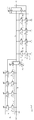
도 1은 본 발명의 일 실시예에 따른 듀티 제어회로를 나타내는 블록도이다. 상기 듀티 제어회로는 바람직하게는 반도체 장치에 구비되어 클록 신호의 듀티를 조절한다. 1 is a block diagram showing a duty control circuit according to an embodiment of the present invention. The duty control circuit is preferably provided in the semiconductor device to adjust the duty of the clock signal.
도 1에 도시된 바와 같이 상기 듀티 제어회로(100)는 클록 입력부(110)와 슬루 제어부(120)를 구비한다. 클록 입력부(110)는 제1 노드(A)를 통해 제공되는 입력 클록신호(CLK1)를 수신하고, 상기 입력 클록신호(CLK1)에 응답하여 제2 노드(B)로 제1 레벨의 전압 또는 제2 레벨의 전압을 제공한다. 바람직하게는, 상기 제1 레벨의 전압은 전원전압(VDD)이고, 제2 레벨의 전압은 접지전압(VSS)일 수 있다. 일예로서, 클록 입력부(110)는 입력 클록신호(CLK1)를 수신하고 이를 인버팅하여 출력하는 인버터를 구비할 수 있다. As shown in FIG. 1, the
슬루 제어부(120)는 상기 제1 레벨의 전압(일예로서, 전원전압(VDD))에 각각 연결되는 복수의 스위치들을 구비할 수 있다. 또는 상기 슬루 제어부(120)는 상기 제2 레벨의 전압(일예로서, 접지전압(VSS))에 각각 연결되는 복수의 스위치들(미도시)을 구비할 수 있다. 슬루 제어부(120)에 구비되는 상기 복수의 스위치들은 스위치들 각각으로 제공되는 제어신호(C[0:n-1])에 의해 스위칭이 제어된다. 상기 제어 신호(C[0:n-1])의 상태에 따라 복수의 스위치들 중 일부의 스위치들이 턴온될 수 있으며, 턴온된 스위치들을 통하여 제1 레벨의 전압 또는 제2 레벨의 전압이 제2 노드(B)로 전달된다.The
입력 클록신호(CLK1)가 로직 하이에서 로직 로우로 천이함에 따라, 상기 입력 클록신호(CLK1)에 응답하여 제2 노드(B)의 전압은 접지전압(VSS)에서 전원전압(VDD)으로 상승한다. 이 경우, 슬루 제어부(120) 내에 구비되는 복수의 스위치들의 선택적인 스위칭 동작에 의하여, 적어도 하나의 전압 경로를 통하여 상기 제2 노드(B)로 전원전압(VDD)을 제공할 수 있다. 많은 수의 전압 경로를 통하여 제2 노드(B)로 전원전압(VDD)을 제공하면 제2 노드(B)의 전압의 라이징 슬루 레이트(rising slew rate)를 증가시킬 수 있다. 이에 따라 슬루 제어부(120) 내에 구비되는 복수의 스위치들의 스위칭 동작에 의하여 제2 노드(B)의 전압의 라이징 슬루 레이트의 조절이 가능하다. As the input clock signal CLK1 transitions from a logic high to a logic low, the voltage of the second node B rises from the ground voltage VSS to the power supply voltage VDD in response to the input clock signal CLK1 . In this case, by the selective switching operation of the plurality of switches provided in the
이와 유사하게, 입력 클록신호(CLK1)가 로직 로우에서 로직 하이로 천이함에 따라, 상기 입력 클록신호(CLK1)에 응답하여 제2 노드(B)의 전압은 전원전압(VDD)에서 접지전압(VSS)으로 하강한다. 슬루 제어부(120)는 접지전압(VSS)에 연결될 수 있으며, 상기와 같은 경우 슬루 제어부(120)내에 구비되는 복수의 스위치들의 선택적인 스위칭 동작에 의하여, 적어도 하나의 전압 경로를 통하여 상기 제2 노드(B)로 접지전압(VSS)을 제공할 수 있다. 많은 수의 전압 경로를 통하여 제2 노드(B)로 접지전압(VSS)을 제공하면 제2 노드(B)의 전압의 폴링 슬루 레이트(falling slew rate)를 증가시킬 수 있다. 이에 따라 슬루 제어부(120) 내에 구비되는 복수의 스 위치들의 스위칭 동작에 의하여 제2 노드(B)의 전압의 폴링 슬루 레이트의 조절이 가능하다. Similarly, as the input clock signal CLK1 transitions from a logic low to a logic high, the voltage of the second node B in response to the input clock signal CLK1 is reduced from the supply voltage VDD to the ground voltage VSS ). The
상기와 같은 라이징 슬루 레이트 또는 폴링 슬루 레이트의 조절을 위하여, 슬루 제어부(120)에 구비되는 복수의 스위치들은 서로 병렬하게 배치된다. 일예로서, 상기 슬루 제어부(120)가 제2 노드(B)의 전압의 라이징 슬루 레이트를 조절하는 경우, 상기 복수의 스위치들은 전원전압(VDD)과 제2 노드(B) 사이에 병렬하게 배치된다. 입력 클록신호(CLK1)가 로직 하이에서 로직 로우로 천이하는 경우, 상기 복수의 스위치들 각각으로 제공되는 제어신호의 상태에 따라 스위치들 각각이 선택적으로 턴온된다. 선택된 스위치들을 통하여 전원전압(VDD)을 제2 노드(B)에 연결함으로써, 제2 노드(B)의 전압의 라이징 슬루 레이트를 조절한다. For the adjustment of the rising slew rate or the falling slew rate as described above, a plurality of switches provided in the
이와 유사하게, 상기 슬루 제어부(120)가 제2 노드(B)의 전압의 폴링 슬루 레이트를 조절하는 경우, 상기 복수의 스위치들은 접지전압(VSS)과 제2 노드(B) 사이에 병렬하게 배치된다. 입력 클록신호(CLK1)가 로직 로우에서 로직 하이로 천이하는 경우, 상기 복수의 스위치들 각각으로 제공되는 제어신호의 상태에 따라 스위치들 각각이 선택적으로 턴온된다. 선택된 스위치들을 통하여 접지전압(VSS)을 제2 노드(B)에 연결함으로써, 제2 노드(B)의 전압의 폴링 슬루 레이트를 조절한다. Similarly, when the
한편, 상기 본 발명의 일실시예에 따른 듀티 제어회로(100)는 클록 출력부(130)와 제어신호 발생부(140)를 더 구비할 수 있으며, 또한 듀티 검출부(150)를 더 구비할 수 있다. 클록 출력부(130)는 인버터 또는 버퍼를 구비할 수 있으며, 제2 노드(B)의 전압을 입력받아 이를 인버팅하거나 버퍼링하고, 인버팅된 신호 또는 버퍼링된 신호를 듀티 조절된 출력 클록신호(CLK2)로서 발생한다. 제어신호 발생부(140)는 슬루 제어부(120) 내에 구비되는 복수의 스위치들의 동작을 제어하기 위한 제어신호(C[0:n-1])를 발생하여 슬루 제어부(120)로 제공한다.The
한편, 바람직하게는, 클록 출력부(130)에서 발생되는 출력 클록신호(CLK2)의 듀티를 검출하고, 상기 듀티를 검출한 결과에 따라 제2 노드(B)의 전압의 라이징 슬루 레이트 또는 폴링 슬루 레이트를 조절하여 듀티를 재조절할 수 있다. 이를 위하여 듀티 검출부(150)는 클록 출력부(130)의 출력단과 연결되는 제3 노드(C)로부터 출력 클록신호(CLK2)를 피드백받으며, 상기 출력 클록신호(CLK2)의 듀티를 검출하여 그 검출결과를 제어신호 발생부(140)로 제공한다. 제어신호 발생부(140)는 듀티 검출결과에 기반하여 상기 제어신호(C[0:n-1])의 값을 변동한다. Preferably, the duty of the output clock signal CLK2 generated in the
상기와 같이 구성될 수 있는 듀티 제어회로(100)의 자세한 동작의 일예를 도 2 내지 도 5를 참조하여 설명하면 다음과 같다.An example of detailed operation of the
도 2는 도 1의 듀티 제어회로의 일 구현예를 나타내는 회로도이다. 특히 도 2의 듀티 제어회로는, 제2 노드(B)의 전압의 라이징 슬루 레이트를 증가시킴으로써 듀티를 조절하는 일예를 나타낸다. 2 is a circuit diagram showing an embodiment of the duty control circuit of FIG. Particularly, the duty control circuit of Fig. 2 shows an example of adjusting the duty by increasing the rising slew rate of the voltage of the second node (B).
도 2에 도시된 바와 같이, 상기 듀티 제어회로(100)는 클록 입력부(110), 슬루 제어부(120) 및 클록 출력부(130)를 구비할 수 있다. 상기 듀티 제어회로(100)는 도 1에서와 같이 제어신호 발생부 및 듀티 검출부를 더 구비할 수 있으나, 설명의 편의상 상기 구성의 도시는 생략하였다. 2, the
클록 입력부(110)는 인버터를 구비하며, 상기 인버터는 전원전압(VDD)에 연 결되는 PMOS 트랜지스터(MP0)와 접지전압(VSS)에 연결되는 NMOS 트랜지스터(MN0)를 구비한다. 클록 입력부(110)는 입력 클록신호(CLK1)를 인버팅하여 출력하며, 일예로서 입력 클록신호(CLK1)가 로직 하이에서 로직 로우로 천이하는 경우 제2 노드(B)로 전원전압(VDD)을 제공하며, 입력 클록신호(CLK1)가 로직 로우에서 로직 하이로 천이하는 경우 제2 노드(B)로 접지전압(VSS)을 제공한다. The
한편 슬루 제어부(120)는 복수의 스위치들을 구비하며, 일예로서 슬루 제어부(120)는 n 개의 제1 스위치들(121)과 n 개의 제2 스위치들(122)을 구비한다. n 개의 제1 스위치들(121)은 제1 PMOS 트랜지스터(MP1_0) 내지 제n PMOS 트랜지스터(MP1_(n-1))을 구비할 수 있다. 상기 n 개의 제1 스위치들(121) 각각의 제1 전극은 전원전압(VDD)에 연결되며, 상기 n 개의 제1 스위치들(121)은 입력 클록신호(CLK1)에 의해 공통적으로 제어된다. Meanwhile, the
한편 n 개의 제2 스위치들(122)은 제(n+1) PMOS 트랜지스터(MP2_0) 내지 제2n PMOS 트랜지스터(MP2_(n-1))를 구비할 수 있으며, 도시된 바와 같이 상기 제(n+1) PMOS 트랜지스터(MP2_0) 내지 제2n PMOS 트랜지스터(MP2_(n-1))는 상기 n 개의 제1 스위치들(121) 각각의 제2 전극과 제2 노드(B) 사이에 연결된다. n 개의 제2 스위치들(122)로는 각각 별도로 조절되는 n 개의 제어신호들(CH[0] 내지 CH[n-1])이 제공되며, n 개의 제2 스위치들(122)에 구비되는 제(n+1) PMOS 트랜지스터(MP2_0) 내지 제2n PMOS 트랜지스터(MP2_(n-1)) 각각은 대응되는 제어신호에 응답하여 스위칭이 제어된다. 일예로서, 제(n+1) PMOS 트랜지스터(MP2_0)는 제어신호 CH[0]에 의해 스위칭이 제어되며, 제(n+2) PMOS 트랜지스터(MP2_1)는 제어신호 CH[1]에 의해 스위칭이 제어된다.The n second switches 122 may include the (n + 1) -th PMOS transistors MP2_0 through the second n-th PMOS transistors MP2_ (n-1) 1) PMOS transistors MP2_0 to MP2_ (n-1) are connected between the second electrode of each of the n first switches 121 and the second node B. n control signals (CH [0] to CH [n-1]) are separately provided to the n second switches 122, and the n control signals n + 1) PMOS transistors MP2_0 through MP2_ (n-1) are controlled in response to a corresponding control signal. For example, the switching of the (n + 1) -th PMOS transistor MP2_0 is controlled by the control signal CH [0] and the switching of the (n + 2) -th PMOS transistor MP2_1 by the control signal CH [ Respectively.
도 3은 도 2의 듀티 제어회로의 동작을 나타내는 파형도이다. 상기 도 2에 도시된 듀티 제어회로(100)의 동작을 도 3을 참조하여 설명하면 다음과 같다. 3 is a waveform diagram showing the operation of the duty control circuit of Fig. The operation of the
입력 클록신호(CLK1)가 로직 로우에서 로직 하이로 천이하여 제1 노드(A)의 전압 레벨이 상승하는 경우, 상기 입력 클록신호(CLK1)에 응답하여 n 개의 제1 스위치들(121)이 턴 오프된다. 이에 따라 제어신호들(CH[0] 내지 CH[n-1])의 상태와 무관하게 슬루 제어부(120)를 통하여 전원전압(VDD)이 제2 노드(B)로 제공되는 것이 차단된다. When the input clock signal CLK1 transitions from a logic low to a logic high and the voltage level of the first node A rises, the n first switches 121 are turned on in response to the input clock signal CLK1, Off. The power supply voltage VDD is prevented from being supplied to the second node B through the
한편, 입력 클록신호(CLK1)가 로직 하이에서 로직 로우로 천이하여 제1 노드(A)의 전압 레벨이 하강하는 경우, 상기 입력 클록신호(CLK1)에 응답하여 n 개의 제1 스위치들(121)이 턴 온된다. 또한 제어신호들(CH[0] 내지 CH[n-1])의 상태에 대응하여 제(n+1) PMOS 트랜지스터(MP2_0) 내지 제2n PMOS 트랜지스터(MP2_(n-1)) 각각의 스위칭이 제어된다. 이에 따라, 상기 n 개의 제2 스위치들(122) 중 턴 온된 스위치들을 통하여 전원전압(VDD)이 제2 노드(B)로 제공된다. On the other hand, when the voltage level of the first node A falls due to the transition of the input clock signal CLK1 from the logic high to the logic low, the n first switches 121 are turned on in response to the input clock signal CLK1, Is turned on. Also, switching of each of the (n + 1) -th PMOS transistors MP2_0 through MP2_ (n-1) in response to the state of the control signals CH [0] through CH [n- Respectively. Accordingly, the power supply voltage VDD is supplied to the second node B through the n second switches 122, which are turned on.
바람직하게는, n 개의 제1 스위치들(121)에 구비되는 PMOS 트랜지스터들의 사이즈(size)를 각각 다르게 구현하고, 또한 n 개의 제2 스위치들(122)에 구비되는 PMOS 트랜지스터들의 사이즈를 각각 다르게 구현한다. 일예로서, 도 2에 도시된 바와 같이, n 개의 제1 스위치들(121)에 구비되는 제1 PMOS 트랜지스터(MP1_0) 내지 제n PMOS 트랜지스터(MP1_(n-1))의 면적이 각각 W, 2W, 4W,...,![]()
![]()
![]()
![]()
![]()
![]()
![]()
![]()
일예로서, n 개의 제어신호들(CH[0] 내지 CH[n-1])의 값이 "000...00" 인 경우, 제(n+1) PMOS 트랜지스터(MP2_0) 내지 제2n PMOS 트랜지스터(MP2_(n-1))는 모두 턴 온된다. 이에 따라 제(n+1) PMOS 트랜지스터(MP2_0) 내지 제2n PMOS 트랜지스터(MP2_(n-1))에 대응하는 경로 모두를 통하여 제2 노드(B)로 전원전압(VDD)이 제공되므로, 제2 노드(B)의 라이징 슬루 레이트가 증가한다. 클록 출력부(130)는 상기 제2 노드(B)의 전압을 반전시켜 출력 클록신호(CLK2)를 발생한다. 도 3에 도시된 제3 노드(C)의 파형과 같이, 제2 노드(B)의 라이징 슬루 레이트가 증가함에 따라 출력 클록신호(CLK2)의 듀티는 감소한다. For example, when the values of the n control signals CH [0] to CH [n-1] are "000 ... 00" (MP2_ (n-1)) are all turned on. Accordingly, since the power supply voltage VDD is supplied to the second node B through all of the paths corresponding to the (n + 1) -th PMOS transistors MP2_0 through MP2_ (n-1) The rising slew rate of the two node (B) increases. The
반면에, n 개의 제어신호들(CH[0] 내지 CH[n-1])의 값이 "111...11" 인 경우, 제(n+1) PMOS 트랜지스터(MP2_0) 내지 제2n PMOS 트랜지스터(MP2_(n-1))는 모두 턴 오프된다. 이에 따라 제(n+1) PMOS 트랜지스터(MP2_0) 내지 제2n PMOS 트랜지스터(MP2_(n-1))를 통하여 제2 노드(B)로 전원전압(VDD)이 제공되는 것이 차단되고, 제2 노드(B)의 라이징 슬루 레이트는 감소한다. 도 3에 도시된 제3 노드(C)의 파형과 같이, 제2 노드(B)의 라이징 슬루 레이트가 감소함에 따라 출력 클록신 호(CLK2)의 듀티는 증가한다. On the other hand, when the values of the n control signals CH [0] to CH [n-1] are "111 ... 11" (MP2_ (n-1)) are all turned off. The supply of the power supply voltage VDD to the second node B is blocked through the (n + 1) -th PMOS transistor MP2_0 through the second n-PMOS transistor MP2_ (n-1) The rising slew rate of (B) decreases. The duty of the output clock signal CLK2 increases as the rising slew rate of the second node B decreases, as is the waveform of the third node C shown in Fig.
n 개의 제어신호들(CH[0] 내지 CH[n-1])은 ![]()
![]()
![]()
![]()
![]()
![]()
상기한 바와 같이 본 발명의 일실시예에에 따른 듀티 제어회로(100)는, 클록신호의 듀티를 프로그래머블하게 단계적으로 조절할 수 있으며 또한 듀티를 정밀하게 조절할 수 있다. 특히 출력 클록신호(CLK2)의 폴링 에지(falling edge)의 슬루를 조절하여 듀티를 조절한다. 이에 따라 클록의 라이징 에지(rising edge)의 변동에 의하여 반도체 시스템 내에서 클록 레이턴시(clock latency)가 변하는 등의 문제를 방지할 수 있다. As described above, the
한편, 도 4는 도 1의 듀티 제어회로의 다른 구현예를 나타내는 회로도이다. 도 4의 듀티 제어회로는, 제2 노드(B)의 전압의 폴링 슬루 레이트를 증가시킴으로써 듀티를 조절하는 일예를 나타낸다. 4 is a circuit diagram showing another embodiment of the duty control circuit of FIG. The duty control circuit of Fig. 4 shows an example of adjusting the duty by increasing the polling slew rate of the voltage of the second node (B).
도 4에 도시된 바와 같이, 상기 듀티 제어회로(100)는 클록 입력부(110), 슬루 제어부(120) 및 클록 출력부(130)를 구비할 수 있다. 클록 입력부(110)는 제1 노드(A)를 통해 제공되는 입력 클록신호(CLK1)를 인버팅하여 출력하는 인버터를 구비할 수 있으며, 또한 클록 출력부(130)는 제2 노드(B)의 전압을 버퍼링하고 이를 출력 클록신호(CLK2)로서 제공하는 버퍼를 구비할 수 있다. The
한편 슬루 제어부(120)는 n 개의 제1 스위치들(121)과 n 개의 제2 스위치들(122)을 구비한다. n 개의 제1 스위치들(121)은 제1 NMOS 트랜지스터(MN1_0) 내지 제n NMOS 트랜지스터(MN1_(n-1))을 구비할 수 있다. 상기 n 개의 제1 스위치들(121) 각각의 제1 전극은 접지전압(VSS)에 연결되며, 상기 n 개의 제1 스위치들(121)은 입력 클록신호(CLK1)에 의해 공통적으로 제어된다. On the other hand, the
한편 n 개의 제2 스위치들(122)은 제(n+1) NMOS 트랜지스터(MN2_0) 내지 제2n NMOS 트랜지스터(MN2_(n-1))를 구비할 수 있으며, 도시된 바와 같이 상기 제(n+1) NMOS 트랜지스터(MN2_0) 내지 제2n NMOS 트랜지스터(MN2_(n-1))는 상기 n 개의 제1 스위치들(121) 각각의 제2 전극과 제2 노드(B) 사이에 연결된다. n 개의 제2 스위치들(122)로는 각각 별도로 조절되는 n 개의 제어신호들(CL[0] 내지 CL[n-1])이 제공되며, n 개의 제2 스위치들(122)에 구비되는 제(n+1) NMOS 트랜지스터(MN2_0) 내지 제2n NMOS 트랜지스터(MN2_(n-1)) 각각은 대응되는 제어신호에 응답하여 스위칭이 제어된다. The n second switches 122 may include the (n + 1) th NMOS transistors MN2_0 through MN2_ (n-1). As shown in the figure, the (n + 1) The NMOS transistors MN2_0 to MN2_ (n-1) are connected between the second electrode of each of the n first switches 121 and the second node B. n control signals CL [0] to CL [n-1] are separately provided to the n second switches 122, and the n control signals CL [ n + 1) NMOS transistors MN2_0 through MN2_ (n-1) are each controlled in response to a corresponding control signal.
도 5은 도 4의 듀티 제어회로의 동작을 나타내는 파형도이다. 상기 도 4에 도시된 듀티 제어회로(100)의 동작을 도 5를 참조하여 설명하면 다음과 같다. 5 is a waveform diagram showing the operation of the duty control circuit of Fig. The operation of the
입력 클록신호(CLK1)가 로직 하이에서 로직 로우로 천이하여 제1 노드(A)의 전압 레벨이 하강하는 경우, 상기 입력 클록신호(CLK1)에 응답하여 n 개의 제1 스위치들(121)이 턴 오프된다. 이에 따라 제어신호들(CL[0] 내지 CL[n-1])의 상태와 무관하게 슬루 제어부(120)를 통하여 접지전압(VSS)이 제2 노드(B)로 제공되는 것 이 차단된다. When the input clock signal CLK1 transitions from a logic high to a logic low and the voltage level of the first node A falls, the n first switches 121 are turned on in response to the input clock signal CLK1, Off. The ground voltage VSS is blocked from being supplied to the second node B through the
한편, 입력 클록신호(CLK1)가 로직 로우에서 로직 하이로 천이하여 제1 노드(A)의 전압 레벨이 상승하는 경우, 상기 입력 클록신호(CLK1)에 응답하여 n 개의 제1 스위치들(121)이 턴 온된다. 또한 n 개의 제2 스위치들(122)에 구비되는 제(n+1) NMOS 트랜지스터(MN2_0) 내지 제2n NMOS 트랜지스터(MN2_(n-1))는, 상기 제어신호들(CL[0] 내지 CL[n-1])의 상태에 따라 선택적으로 턴 온된다. 이에 따라 상기 n 개의 제2 스위치들(122) 중 턴 온된 스위치들을 통하여 접지전압(VSS)이 제2 노드(B)로 제공된다. 앞서 설명한 바와 같이 n 개의 제1 스위치들(121)은 서로 사이즈를 달리 구현하는 것이 바람직하며, 또한 n 개의 제2 스위치들(122)은 서로 그 사이를 달리 구현하는 것이 바람직하다.On the other hand, when the voltage level of the first node A rises due to the transition of the input clock signal CLK1 from a logic low to a logic high, n first switches 121 are turned on in response to the input clock signal CLK1, Is turned on. The (n + 1) th NMOS transistors MN2_0 to MN2_ (n-1) included in the n second switches 122 are controlled by the control signals CL [0] to CL [n-1]). Accordingly, the ground voltage VSS is supplied to the second node B through the n second switches 122, which are turned on. As described above, it is preferable that the n first switches 121 are different in size from each other, and the n second switches 122 are preferably implemented differently from each other.
입력 클록신호(CLK1)가 로직 로우에서 로직 하이로 천이하고 n 개의 제1 스위치들(121)이 턴 온되는 경우, n 개의 제어신호들(CL[0] 내지 CL[n-1])의 상태에 대응하여 제2 노드(B)의 폴링 슬루 레이트가 조절된다. 일예로서, n 개의 제어신호들(CL[0] 내지 CL[n-1])의 값이 "000...00" 인 경우, 제(n+1) NMOS 트랜지스터(MN2_0) 내지 제2n NMOS 트랜지스터(MN2_(n-1)) 모두가 턴 오프된다. 이에 따라 제2 노드(B)의 폴링 슬루 레이트가 감소한다. 클록 출력부(130)는 상기 제2 노드(B)의 전압을 버퍼링하여 출력 클록신호(CLK2)를 발생한다. 도 5에 도시된 제3 노드(C)의 파형과 같이, 제2 노드(B)의 폴링 슬루 레이트가 감소함에 따라 출력 클록신호(CLK2)의 듀티는 증가한다. When the input clock signal CLK1 transitions from a logic low to a logic high and n first switches 121 are turned on, the state of the n control signals CL [0] to CL [n-1] The polling slew rate of the second node B is adjusted. For example, when the values of the n control signals CL [0] to CL [n-1] are "000 ... 00 ", the (n + 1) -th NMOS transistors MN2_0- (MN2_ (n-1)) are turned off. Whereby the polling slew rate of the second node B decreases. The
반면에, n 개의 제어신호들(CL[0] 내지 CL[n-1])의 값이 "111...11" 인 경 우, 제(n+1) NMOS 트랜지스터(MN2_0) 내지 제2n NMOS 트랜지스터(MN2_(n-1))는 모두 턴 온된다. 이에 따라 제2 노드(B)의 폴링 슬루 레이트가 증가하고 출력 클록신호(CLK2)의 듀티는 감소하게 된다. On the other hand, when the values of the n control signals CL [0] to CL [n-1] are "111 ... 11" The transistor MN2_ (n-1) is all turned on. As a result, the polling slew rate of the second node B increases and the duty of the output clock signal CLK2 decreases.
도 4 및 도 5에 도시된 듀티 제어회로(100)의 특징에 따르면, 제2 노드(B)의 폴링 슬루 레이트 또한 ![]()
![]()
![]()
![]()
도 6은 본 발명의 다른 실시예에 따른 듀티 제어회로를 나타내는 블록도이다. 도 6에 도시된 본 발명의 일 실시예에 따른 듀티 제어회로(200)는, 제1 클록 입력부(210), 제1 슬루 제어부(220), 제2 클록 입력부(230), 제2 슬루 제어부(240) 및 클록 출력부(250)를 구비할 수 있다. 또한 상기 듀티 제어회로(200)는 제어신호 발생부(260) 및 듀티 검출부(270)를 더 구비할 수 있다. 상기 듀티 제어회로(200)에 구비되는 구성 요소들의 동작중 앞서 도 1에 도시된 구성과 동일한 것에 대해서는 그 동작 또한 유사하므로 이에 대한 자세한 설명은 생략한다. 6 is a block diagram showing a duty control circuit according to another embodiment of the present invention. The
제1 클록 입력부(210)는 제1 노드(A)를 통해 제공되는 입력 클록신호(CLK1)를 수신하고 이를 버퍼링하거나 인버팅하여 제2 노드(B1)로 제공한다. 바람직하게는 제1 클록 입력부(210)는 인버터를 구비하며, 입력 클록신호(CLK1)의 하강 천이에 응답하여 제2 노드(B1)로 전원전압(VDD)를 제공하며, 입력 클록신호(CLK1)의 상승 천이에 응답하여 제2 노드(B1)로 접지전압(VSS)를 제공한다. The first
제1 슬루 제어부(220)는 전원전압(VDD) 또는 접지전압(VSS)과 전기적으로 연결되어, 소정의 제1 제어신호(CH[0:n-1])에 응답하여 상기 전원전압(VDD) 또는 접지전압(VSS)을 제2 노드(B1)로 제공한다. 일예로서 제1 슬루 제어부(220)가 전원전압(VDD)에 전기적으로 연결되는 경우, 제1 슬루 제어부(220)는 상기 전원전압(VDD)과 제2 노드(B1) 사이에 병렬하게 배치되는 복수의 제1 스위치들을 구비한다. 상기 복수의 제1 스위치들은 제1 제어신호(CH[0:n-1])에 응답하여 선택적으로 스위칭되며, 선택된 스위치들을 통하여 상기 전원전압(VDD)이 제2 노드(B1)로 제공된다.The first
제2 클록 입력부(230)는 제2 노드(B1)의 신호를 입력받으며, 제2 노드(B1)의 신호에 응답하여 제3 노드(B2)로 신호를 전달한다. 일예로서, 제2 클록 입력부(230)는 제2 노드(B1)의 신호를 입력받아 이를 인버팅하거나 버퍼링하여 제3 노드(B2)로 출력한다. 바람직하게는, 제2 클록 입력부(230)는 제2 노드(B1)의 신호를 입력받아 이를 인버팅하여 출력하는 인버터를 구비할 수 있다. The second
제2 슬루 제어부(240)는 전원전압(VDD) 또는 접지전압(VSS)과 전기적으로 연결되며, 소정의 제2 제어신호(CL[0:n-1])에 응답하여 상기 전원전압(VDD) 또는 접지전압(VSS)을 제3 노드(B2)로 제공한다. 바람직하게는, 제1 슬루 제어부(220)가 전원전압(VDD)에 전기적으로 연결되는 경우, 제2 슬루 제어부(240)는 접지전압(VSS)에 전기적으로 연결된다. 제2 슬루 제어부(240)는 상기 접지전압(VSS)과 제3 노드(B2) 사이에 병렬하게 배치되는 복수의 제2 스위치들을 구비한다. 상기 복수의 제2 스위치들은 제2 제어신호(CL[0:n-1])에 응답하여 선택적으로 스위칭되며, 선택된 스위치들을 통하여 상기 접지전압(VSS)이 제3 노드(B2)로 제공된다.The second
클록 출력부(250)는 제3 노드(B2)의 신호를 입력받아 이를 버퍼링하거나 인버팅하여 출력한다. 상기 버퍼링 또는 인버팅된 신호를 듀티 조절된 출력 클록신호(CLK2)로서 발생한다. 또한 제어신호 발생부(260)는 제1 슬루 제어부(220) 내에 구비되는 복수의 제1 스위치들의 동작을 제어하기 위한 제1 제어신호(CH[0:n-1])를 발생하며, 제2 슬루 제어부(240) 내에 구비되는 복수의 제2 스위치들의 동작을 제어하기 위한 제2 제어신호(CL[0:n-1])를 발생한다.The
한편, 상기 클록 출력부(250)에서 발생된 출력 클록신호(CLK2)의 듀티를 검출하여, 상기 검출 결과에 따라 제1 제어신호(CH[0:n-1]) 및 제2 제어신호(CL[0:n-1])를 적절히 조절할 필요가 있다. 이에 따라 듀티 검출부(270)는 클록 출력부(250)의 출력단에 연결되는 제4 노드(C)로부터 출력 클록신호(CLK2)를 피드백받으며, 상기 출력 클록신호(CLK2)의 듀티를 검출하여 그 검출결과를 제어신호 발생부(260)로 제공한다. 제어신호 발생부(260)는 듀티 검출결과에 기반하여 상기 제1 제어신호(CH[0:n-1]) 및 제2 제어신호(CL[0:n-1])의 값을 변동한다. On the other hand, the duty of the output clock signal CLK2 generated in the
상기와 같이 구성될 수 있는 듀티 제어회로(200)의 자세한 동작을 도 7 및 도 8을 참조하여 설명한다. 도 7 및 도 8은 도 6의 듀티 제어회로(200)의 일 실시예를 나타내는 것으로서, 특히 제1 슬루 제어부(220)가 제2 노드(B3)의 전압의 라이징 슬루 레이트를 조절하고, 제2 슬루 제어부(240)가 제3 노드(B2)의 전압의 폴링 슬루 레이트를 조절하는 경우를 나타낸다. 그러나 본 발명의 실시예는 이에 한정되는 것이 아니다. 다른 동작의 일예로서, 제1 슬루 제어부(220)가 제2 노드(B3)의 전압의 폴링 슬루 레이트를 조절하고, 제2 슬루 제어부(240)가 제3 노드(B2)의 전압의 라이징 슬루 레이트를 조절하도록 구성하여도 무방하다. The detailed operation of the
도 7은 도 6의 듀티 제어회로의 일 구현예를 나타내는 회로도이다. 도 7에 도시된 바와 같이 제1 슬루 제어부(220)는, 제1 내지 제n PMOS 트랜지스터들(MP1_0 내지 MP1_(n-1))과, 제(n+1) 내지 제2n PMOS 트랜지스터들(MP2_0 내지 MP2_(n-1))을 구비한다. 또한 바람직하게는, 제1 내지 제n PMOS 트랜지스터들(MP1_0 내지 MP1_(n-1)) 각각의 사이즈를 다르게 구현하며, 또한 제(n+1) 내지 제2n PMOS 트랜지스터들(MP2_0 내지 MP2_(n-1)) 각각의 사이즈를 다르게 구현한다. 일예로서, 제1 내지 제n PMOS 트랜지스터들(MP1_0 내지 MP1_(n-1))의 면적이 각각 W, 2W, 4W,...,![]()
![]()
![]()
![]()
입력 클록신호(CLK1)가 로직 하이에서 로직 로우로 천이하는 경우, 상기 입력 클록신호(CLK1)에 응답하여 동작하는 제1 내지 제n PMOS 트랜지스터들(MP1_0 내지 MP1_(n-1))은 모두 턴 온된다. 한편, n 개의 제1 제어신호(CH[0:n-1]) 각각에 의하여 동작하는 제(n+1) 내지 제2n PMOS 트랜지스터들(MP2_0 내지 MP2_(n-1))은, 상기 제1 제어신호(CH[0:n-1])의 상태에 대응하여 선택적으로 턴 온된다. 일예로서 상기 제1 제어신호(CH[0:n-1])가 "000...00" 값을 갖는 경우 상기 제(n+1) 내지 제2n PMOS 트랜지스터들(MP2_0 내지 MP2_(n-1))은 모두 턴 온되며, 상기 제1 제어신호(CH[0:n-1])가 "111...11" 값을 갖는 경우 상기 제(n+1) 내지 제2n PMOS 트랜지스터들(MP2_0 내지 MP2_(n-1))은 모두 턴 오프된다.When the input clock signal CLK1 transitions from a logic high to a logic low, the first through n-th PMOS transistors MP1_0 through MP1_ (n-1) operating in response to the input clock signal CLK1 are all turned Is turned on. On the other hand, the (n + 1) th to the 2n-th PMOS transistors MP2_0 to MP2_ (n-1) operated by each of the n first control signals CH [0: n- Is selectively turned on in response to the state of the control signal CH [0: n-1]. For example, when the first control signal CH [0: n-1] has a value of 000 ... 00, the (n + 1) th to the 2n PMOS transistors MP2_0 to MP2_ ) Are all turned on and the (n + 1) th to the 2 < n > PMOS transistors MP2_0 (MP2_0) are turned on when the first control signal CH [ To MP2_ (n-1) are all turned off.
상기 제1 제어신호(CH[0:n-1])의 값을 조절함으로써, 제2 노드(B1)의 전압의 라이징 슬루 레이트를 조절할 수 있다. 일예로서, 제1 제어신호(CH[0:n-1])의 값을 "000...00"으로부터 "111...11" 까지 조절함으로써, 상기 제2 노드(B1)의 전압의 라이징 슬루 레이트를 ![]()
![]()
한편, 상기 제2 노드(B1)의 전압은 제2 클록 입력부(230)의 입력 신호로서 제공되며, 제2 클록 입력부(230)는 제2 노드(B1)의 전압을 인버팅하여 제3 노드(B2)로 출력한다. 상기 제2 슬루 제어부(240)는 제1 내지 제n NMOS 트랜지스터들(MN1_0 내지 MN1_(n-1))과, 제(n+1) 내지 제2n NMOS 트랜지스터들(MN2_0 내지 MN2_(n-1))을 구비한다. Meanwhile, the voltage of the second node B1 is provided as an input signal to the second
상기 제2 노드(B1)의 전압이 로직 로우에서 로직 하이로 천이하는 경우, 상기 제2 노드(B1)의 전압에 응답하여 동작하는 제1 내지 제n NMOS 트랜지스터들(MN1_0 내지 MN1_(n-1))은 모두 턴 온된다. 한편, n 개의 제2 제어신호(CL[0:n-1]) 각각에 의하여 동작하는 제(n+1) 내지 제2n NMOS 트랜지스터들(MN2_0 내지 MN2_(n-1))은, 상기 제2 제어신호(CL[0:n-1])의 상태에 대응하여 선택적으로 턴 온된다. The first through n-th NMOS transistors MN1_0 through MN1_ (n-1) operate in response to the voltage of the second node B1 when the voltage of the second node B1 transitions from a logic low to a logic high. ) Are all turned on. On the other hand, the (n + 1) th to the 2n-th NMOS transistors MN2_0 to MN2_ (n-1) operated by each of the n second control signals CL [0: n-1] Is selectively turned on in response to the state of the control signal CL [0: n-1].
상기 제2 제어신호(CL[0:n-1])의 값을 조절함으로써, 제3 노드(B2)의 전압의 폴링 슬루 레이트를 조절할 수 있다. 일예로서, 제2 제어신호(CL[0:n-1])의 값을 "000...00"으로부터 "111...11" 까지 조절함으로써, 상기 제3 노드(B2)의 전압의 폴링 슬루 레이트를 ![]()
![]()
즉, 듀티 제어회로(200)가 구비되는 반도체 장치의 초기 동작시 "000...00"에 해당하는 제2 제어신호(CL[0:n-1])가 발생되도록 하고, 상기 제2 제어신호(CL[0:n-1])의 값을 점차 증가시킴으로써 상기 출력 클록신호(CLK2)의 듀티를 점차 감소시킬 수 있다. That is, the second control signal CL [0: n-1] corresponding to "000 ... 00" is generated in the initial operation of the semiconductor device having the
도 8a,b는 도 6의 듀티 제어회로의 동작을 나타내는 파형도이다. 도 8a는 제1 슬루 제어부(220)에 의한 동작을 나타내며, 도 8b는 제2 슬루 제어부(240)에 의한 동작을 나타낸다. 도 8a에 도시된 바와 같이, 제1 제어신호(CH[0:n-1])가 "000..00"에서 "111..11"로 증가함에 따라, 제2 노드(B1)의 전압의 라이징 슬루 레 이트는 점차 감소한다. 또한 제2 노드(B1)의 전압의 라이징 슬루 레이트가 감소함에 따라, 상기 제2 노드(B1)의 전압의 인버팅된 값에 대응하는 출력 클록신호(CLK2)의 듀티는 점차 증가한다. 8A and 8B are waveform diagrams showing the operation of the duty control circuit of FIG. 8A shows operation by the first
또한 도 8b에 도시된 바와 같이, 제2 제어신호(CL[0:n-1])가 "000..00"에서 "111..11"로 증가함에 따라, 제3 노드(B2)의 전압의 폴링 슬루 레이트는 점차 증가한다. 또한 제3 노드(B2)의 전압의 폴링 슬루 레이트가 증가함에 따라, 상기 제3 노드(B2)의 전압의 버퍼링된 값에 대응하는 출력 클록신호(CLK2)의 듀티는 점차 감소한다. As shown in FIG. 8B, as the second control signal CL [0: n-1] increases from "000..00" to "111..11", the voltage of the third node B2 The polling slew rate of < / RTI > Also, as the polling slew rate of the voltage of the third node B2 increases, the duty of the output clock signal CLK2 corresponding to the buffered value of the voltage of the third node B2 gradually decreases.
상술한 바와 같은 도 6의 듀티 제어회로(200)에 따르면, 도 2에 도시된 듀티 제어회로에 대응하는 제1 듀티 제어회로와, 도 4에 도시된 듀티 제어회로에 대응하는 제2 듀티 제어회로가 서로 결합된 구조를 갖는다. 제1 듀티 제어회로의 클록 출력부와 제2 듀티 제어회로의 클록 입력부는 모두 인버터로 구현될 수 있으므로, 상기 도 6의 제2 클록 입력부(230)는 제1 듀티 제어회로 및 제2 듀티 제어회로에 의해 공유되도록 구성될 수 있다. According to the
상기 도 6의 듀티 제어회로(200)는 클록 신호의 듀티를 프로그래머블하게 증가시킬 수 있으며, 또한 프로그래머블하게 감소시킬 수 있다. 즉, 듀티 제어회로(200)가 포함되는 반도체 장치의 초기 동작시 제1 제어신호(CH[0:n-1]) 및 제2 제어신호(CL[0:n-1])가 각각 "000..00" 값을 갖도록 한다. 이후, 클록 신호의 듀티를 증가시키기 위해서는 제1 제어신호(CH[0:n-1])의 값을 점차 증가시킨다. 또한 클록 신호의 듀티를 감소시키기 위해서는 제2 제어신호(CL[0:n-1])의 값을 점차 증 가시킨다. The
상기와 같이 구성되는 경우, 제1 제어신호(CH[0:n-1]) 및 제2 제어신호(CL[0:n-1])를 조절하는 것에 의하여, 클록 신호의 듀티를 정밀하게 조절할 수 있으며 또한 상기 듀티를 많은 수의 단계로 프로그래머블하게 조절할 수 있다. 또한 도 8a,b에 도시된 바와 같이, 듀티를 증가시키거나 감소시키는 어떠한 경우에도 출력 클록 신호의 라이징 에지(rising edge)의 기준은 변하지 않는다. 이에 따라 상기 듀티 제어회로가 구비되는 반도체 장치에서 듀티 조절로 인한 클록 레이턴시(clock latency) 변화 등의 문제가 발생하지 않게 된다. The duty of the clock signal can be precisely adjusted by adjusting the first control signal CH [0: n-1] and the second control signal CL [0: n-1] And the duty can be programmably adjusted in a number of steps. Also, as shown in Figs. 8A and 8B, the reference of the rising edge of the output clock signal does not change in any case in which the duty is increased or decreased. Accordingly, the semiconductor device including the duty control circuit does not suffer from a problem such as a change in clock latency due to duty control.
본 발명은 도면에 도시된 실시예를 참고로 설명되었으나 이는 예시적인 것에 불과하며, 본 기술 분야의 통상의 지식을 가진 자라면 이로부터 다양한 변형 및 균등한 다른 실시예가 가능하다는 점을 이해할 것이다. 따라서, 본 발명의 진정한 기술적 보호 범위는 첨부된 특허청구범위의 기술적 사상에 의하여 정해져야 할 것이다.While the present invention has been described with reference to exemplary embodiments, it is to be understood that the invention is not limited to the disclosed exemplary embodiments, but, on the contrary, is intended to cover various modifications and equivalent arrangements included within the spirit and scope of the appended claims. Accordingly, the true scope of the present invention should be determined by the technical idea of the appended claims.
도 1은 본 발명의 일 실시예에 따른 듀티 제어회로를 나타내는 블록도이다. 1 is a block diagram showing a duty control circuit according to an embodiment of the present invention.
도 2는 도 1의 듀티 제어회로의 일 구현예를 나타내는 회로도이다.2 is a circuit diagram showing an embodiment of the duty control circuit of FIG.
도 3은 도 2의 듀티 제어회로의 동작을 나타내는 파형도이다.3 is a waveform diagram showing the operation of the duty control circuit of Fig.
도 4는 도 1의 듀티 제어회로의 다른 구현예를 나타내는 회로도이다.4 is a circuit diagram showing another embodiment of the duty control circuit of FIG.
도 5는 도 4의 듀티 제어회로의 동작을 나타내는 파형도이다.5 is a waveform diagram showing the operation of the duty control circuit of FIG.
도 6은 본 발명의 다른 실시예에 따른 듀티 제어회로를 나타내는 블록도이다. 6 is a block diagram showing a duty control circuit according to another embodiment of the present invention.
도 7은 도 6의 듀티 제어회로의 일 구현예를 나타내는 회로도이다.7 is a circuit diagram showing an embodiment of the duty control circuit of Fig.
도 8a,b는 도 6의 듀티 제어회로의 동작을 나타내는 파형도이다.8A and 8B are waveform diagrams showing the operation of the duty control circuit of FIG.
* 도면의 주요부분에 대한 부호의 설명 * Description of the Related Art [0002]
100: 듀티 제어회로100: duty control circuit
110: 클록 입력부110: clock input unit
120: 슬루 제어부120: Slew control unit
130: 클록 출력부130: Clock output section
140: 제어신호 발생부140: Control signal generator
150: 듀티 검출부150: duty detector
Claims (25)
Priority Applications (2)
| Application Number | Priority Date | Filing Date | Title |
|---|---|---|---|
| KR1020080092944A KR101535224B1 (en) | 2008-09-22 | 2008-09-22 | Duty control circuit and semiconductor device having the same |
| US12/585,680 US7994835B2 (en) | 2008-09-22 | 2009-09-22 | Duty control circuit and semiconductor device having the same |
Applications Claiming Priority (1)
| Application Number | Priority Date | Filing Date | Title |
|---|---|---|---|
| KR1020080092944A KR101535224B1 (en) | 2008-09-22 | 2008-09-22 | Duty control circuit and semiconductor device having the same |
Publications (2)
| Publication Number | Publication Date |
|---|---|
| KR20100033876A KR20100033876A (en) | 2010-03-31 |
| KR101535224B1 true KR101535224B1 (en) | 2015-07-08 |
Family
ID=42037000
Family Applications (1)
| Application Number | Title | Priority Date | Filing Date |
|---|---|---|---|
| KR1020080092944A KR101535224B1 (en) | 2008-09-22 | 2008-09-22 | Duty control circuit and semiconductor device having the same |
Country Status (2)
| Country | Link |
|---|---|
| US (1) | US7994835B2 (en) |
| KR (1) | KR101535224B1 (en) |
Families Citing this family (6)
| Publication number | Priority date | Publication date | Assignee | Title |
|---|---|---|---|---|
| JP2010226173A (en) * | 2009-03-19 | 2010-10-07 | Elpida Memory Inc | Duty detection circuit, clock generation circuit including the duty detection circuit, and semiconductor device |
| US8779818B2 (en) * | 2012-11-06 | 2014-07-15 | Texas Instruments Incorporated | Optimizing pre-driver control for digital integrated circuits |
| KR102323569B1 (en) | 2015-09-30 | 2021-11-08 | 삼성전자주식회사 | Data processing circuit for controlling sampling point independently and data processing system including the same |
| KR102280437B1 (en) | 2015-10-14 | 2021-07-22 | 삼성전자주식회사 | Delay cell and delay line having the same |
| CN111192609B (en) * | 2018-11-15 | 2024-09-06 | 长鑫存储技术有限公司 | Clock duty cycle calibration circuit and calibration method |
| US11005467B1 (en) * | 2020-05-18 | 2021-05-11 | Realtek Semiconductor Corp. | Low-noise duty cycle correction circuit and method thereof |
Citations (1)
| Publication number | Priority date | Publication date | Assignee | Title |
|---|---|---|---|---|
| US20080052440A1 (en) * | 1999-10-19 | 2008-02-28 | Horowitz Mark A | Integrated Circuit Memory Device and Signaling Method with Topographic Dependent Signaling |
Family Cites Families (5)
| Publication number | Priority date | Publication date | Assignee | Title |
|---|---|---|---|---|
| US5959481A (en) * | 1997-02-18 | 1999-09-28 | Rambus Inc. | Bus driver circuit including a slew rate indicator circuit having a one shot circuit |
| US6760857B1 (en) * | 2000-02-18 | 2004-07-06 | Rambus Inc. | System having both externally and internally generated clock signals being asserted on the same clock pin in normal and test modes of operation respectively |
| TWI283515B (en) * | 2002-10-02 | 2007-07-01 | Via Tech Inc | Method and device for adjusting reference level |
| US6670838B1 (en) * | 2002-11-05 | 2003-12-30 | Chrontel, Inc. | Digital clock adaptive duty cycle circuit |
| KR100790992B1 (en) | 2006-06-21 | 2008-01-03 | 삼성전자주식회사 | Duty cycle correction circuit and duty cycle correction method using delay cells |
-
2008
- 2008-09-22 KR KR1020080092944A patent/KR101535224B1/en active IP Right Grant
-
2009
- 2009-09-22 US US12/585,680 patent/US7994835B2/en active Active
Patent Citations (1)
| Publication number | Priority date | Publication date | Assignee | Title |
|---|---|---|---|---|
| US20080052440A1 (en) * | 1999-10-19 | 2008-02-28 | Horowitz Mark A | Integrated Circuit Memory Device and Signaling Method with Topographic Dependent Signaling |
Also Published As
| Publication number | Publication date |
|---|---|
| KR20100033876A (en) | 2010-03-31 |
| US20100073059A1 (en) | 2010-03-25 |
| US7994835B2 (en) | 2011-08-09 |
Similar Documents
| Publication | Publication Date | Title |
|---|---|---|
| US7091761B2 (en) | Impedance controlled output driver | |
| KR101535224B1 (en) | Duty control circuit and semiconductor device having the same | |
| US9331702B2 (en) | Apparatuses and methods for compensating for power supply sensitivities of a circuit in a clock path | |
| US9123406B2 (en) | Semiconductor memory device capable of selectively enabling/disabling a first input unit and a second input unit in response to a first and second internal clock in a gear-down mode | |
| KR100327135B1 (en) | delay circuit and semiconductor memory device using this circuit | |
| US8344783B2 (en) | Delay circuit and method for delaying signal | |
| US9571100B2 (en) | Clock buffers with pulse drive capability for power efficiency | |
| KR101848758B1 (en) | Semiconductor device and method operation of the same | |
| JP2013157670A (en) | Driver circuit | |
| US7965120B2 (en) | Digitally controlled CML buffer | |
| KR20090126592A (en) | Output driver | |
| US8149037B2 (en) | Clock duty correction circuit | |
| JP5471272B2 (en) | Clock signal amplifier circuit, clock signal amplifier circuit control method, and clock signal distribution circuit | |
| KR20030021429A (en) | Phase splitter circuit | |
| US20090039932A1 (en) | Delay circuit of semiconductor memory apparatus | |
| JP2007067819A (en) | Delay adjusting circuit and synchronous type semiconductor device equipped with the circuit | |
| JP2007300302A (en) | Waveform width adjusting circuit | |
| KR100622762B1 (en) | Data output buffer | |
| KR100851990B1 (en) | Command Buffer for Semiconductor Memory Apparatus | |
| KR100739994B1 (en) | Input circuit of semiconductor device | |
| US20110169542A1 (en) | Delay circuit of semiconductor memory apparatus and method for delaying | |
| US7218161B2 (en) | Substantially temperature independent delay chain | |
| CN118151706A (en) | Circuit and method of operating the circuit | |
| KR20070016857A (en) | Setup hold time control circuit | |
| KR20100013167A (en) | Semiconductor device for maintaining data access time |
Legal Events
| Date | Code | Title | Description |
|---|---|---|---|
| PA0109 | Patent application |
Patent event code: PA01091R01D Comment text: Patent Application Patent event date: 20080922 |
|
| PG1501 | Laying open of application | ||
| A201 | Request for examination | ||
| PA0201 | Request for examination |
Patent event code: PA02012R01D Patent event date: 20130806 Comment text: Request for Examination of Application Patent event code: PA02011R01I Patent event date: 20080922 Comment text: Patent Application |
|
| E902 | Notification of reason for refusal | ||
| PE0902 | Notice of grounds for rejection |
Comment text: Notification of reason for refusal Patent event date: 20141022 Patent event code: PE09021S01D |
|
| E701 | Decision to grant or registration of patent right | ||
| PE0701 | Decision of registration | ||
| GRNT | Written decision to grant | ||
| PR0701 | Registration of establishment |
Comment text: Registration of Establishment Patent event date: 20150702 Patent event code: PR07011E01D |
|
| PR1002 | Payment of registration fee |
Payment date: 20150703 End annual number: 3 Start annual number: 1 |
|
| PG1601 | Publication of registration | ||
| FPAY | Annual fee payment |
Payment date: 20180629 Year of fee payment: 4 |
|
| PR1001 | Payment of annual fee |
Payment date: 20180629 Start annual number: 4 End annual number: 4 |
|
| PR1001 | Payment of annual fee |
Payment date: 20200630 Start annual number: 6 End annual number: 6 |
|
| PR1001 | Payment of annual fee |
Payment date: 20210628 Start annual number: 7 End annual number: 7 |
|
| PR1001 | Payment of annual fee |
Payment date: 20220622 Start annual number: 8 End annual number: 8 |
|
| PR1001 | Payment of annual fee |
Payment date: 20230621 Start annual number: 9 End annual number: 9 |
|
| PR1001 | Payment of annual fee |
Payment date: 20240626 Start annual number: 10 End annual number: 10 |