KR101489327B1 - Method of forming a material layer and method of fabricating a memory device - Google Patents
Method of forming a material layer and method of fabricating a memory device Download PDFInfo
- Publication number
- KR101489327B1 KR101489327B1 KR20080045072A KR20080045072A KR101489327B1 KR 101489327 B1 KR101489327 B1 KR 101489327B1 KR 20080045072 A KR20080045072 A KR 20080045072A KR 20080045072 A KR20080045072 A KR 20080045072A KR 101489327 B1 KR101489327 B1 KR 101489327B1
- Authority
- KR
- South Korea
- Prior art keywords
- precursor
- central element
- cycle
- substrate
- formula
- Prior art date
- Legal status (The legal status is an assumption and is not a legal conclusion. Google has not performed a legal analysis and makes no representation as to the accuracy of the status listed.)
- Active
Links
Images


Classifications
-
- C—CHEMISTRY; METALLURGY
- C23—COATING METALLIC MATERIAL; COATING MATERIAL WITH METALLIC MATERIAL; CHEMICAL SURFACE TREATMENT; DIFFUSION TREATMENT OF METALLIC MATERIAL; COATING BY VACUUM EVAPORATION, BY SPUTTERING, BY ION IMPLANTATION OR BY CHEMICAL VAPOUR DEPOSITION, IN GENERAL; INHIBITING CORROSION OF METALLIC MATERIAL OR INCRUSTATION IN GENERAL
- C23C—COATING METALLIC MATERIAL; COATING MATERIAL WITH METALLIC MATERIAL; SURFACE TREATMENT OF METALLIC MATERIAL BY DIFFUSION INTO THE SURFACE, BY CHEMICAL CONVERSION OR SUBSTITUTION; COATING BY VACUUM EVAPORATION, BY SPUTTERING, BY ION IMPLANTATION OR BY CHEMICAL VAPOUR DEPOSITION, IN GENERAL
- C23C16/00—Chemical coating by decomposition of gaseous compounds, without leaving reaction products of surface material in the coating, i.e. chemical vapour deposition [CVD] processes
- C23C16/22—Chemical coating by decomposition of gaseous compounds, without leaving reaction products of surface material in the coating, i.e. chemical vapour deposition [CVD] processes characterised by the deposition of inorganic material, other than metallic material
- C23C16/30—Deposition of compounds, mixtures or solid solutions, e.g. borides, carbides, nitrides
- C23C16/305—Sulfides, selenides, or tellurides
-
- C—CHEMISTRY; METALLURGY
- C23—COATING METALLIC MATERIAL; COATING MATERIAL WITH METALLIC MATERIAL; CHEMICAL SURFACE TREATMENT; DIFFUSION TREATMENT OF METALLIC MATERIAL; COATING BY VACUUM EVAPORATION, BY SPUTTERING, BY ION IMPLANTATION OR BY CHEMICAL VAPOUR DEPOSITION, IN GENERAL; INHIBITING CORROSION OF METALLIC MATERIAL OR INCRUSTATION IN GENERAL
- C23C—COATING METALLIC MATERIAL; COATING MATERIAL WITH METALLIC MATERIAL; SURFACE TREATMENT OF METALLIC MATERIAL BY DIFFUSION INTO THE SURFACE, BY CHEMICAL CONVERSION OR SUBSTITUTION; COATING BY VACUUM EVAPORATION, BY SPUTTERING, BY ION IMPLANTATION OR BY CHEMICAL VAPOUR DEPOSITION, IN GENERAL
- C23C16/00—Chemical coating by decomposition of gaseous compounds, without leaving reaction products of surface material in the coating, i.e. chemical vapour deposition [CVD] processes
- C23C16/06—Chemical coating by decomposition of gaseous compounds, without leaving reaction products of surface material in the coating, i.e. chemical vapour deposition [CVD] processes characterised by the deposition of metallic material
- C23C16/16—Chemical coating by decomposition of gaseous compounds, without leaving reaction products of surface material in the coating, i.e. chemical vapour deposition [CVD] processes characterised by the deposition of metallic material from metal carbonyl compounds
-
- C—CHEMISTRY; METALLURGY
- C23—COATING METALLIC MATERIAL; COATING MATERIAL WITH METALLIC MATERIAL; CHEMICAL SURFACE TREATMENT; DIFFUSION TREATMENT OF METALLIC MATERIAL; COATING BY VACUUM EVAPORATION, BY SPUTTERING, BY ION IMPLANTATION OR BY CHEMICAL VAPOUR DEPOSITION, IN GENERAL; INHIBITING CORROSION OF METALLIC MATERIAL OR INCRUSTATION IN GENERAL
- C23C—COATING METALLIC MATERIAL; COATING MATERIAL WITH METALLIC MATERIAL; SURFACE TREATMENT OF METALLIC MATERIAL BY DIFFUSION INTO THE SURFACE, BY CHEMICAL CONVERSION OR SUBSTITUTION; COATING BY VACUUM EVAPORATION, BY SPUTTERING, BY ION IMPLANTATION OR BY CHEMICAL VAPOUR DEPOSITION, IN GENERAL
- C23C16/00—Chemical coating by decomposition of gaseous compounds, without leaving reaction products of surface material in the coating, i.e. chemical vapour deposition [CVD] processes
- C23C16/06—Chemical coating by decomposition of gaseous compounds, without leaving reaction products of surface material in the coating, i.e. chemical vapour deposition [CVD] processes characterised by the deposition of metallic material
- C23C16/18—Chemical coating by decomposition of gaseous compounds, without leaving reaction products of surface material in the coating, i.e. chemical vapour deposition [CVD] processes characterised by the deposition of metallic material from metallo-organic compounds
-
- C—CHEMISTRY; METALLURGY
- C23—COATING METALLIC MATERIAL; COATING MATERIAL WITH METALLIC MATERIAL; CHEMICAL SURFACE TREATMENT; DIFFUSION TREATMENT OF METALLIC MATERIAL; COATING BY VACUUM EVAPORATION, BY SPUTTERING, BY ION IMPLANTATION OR BY CHEMICAL VAPOUR DEPOSITION, IN GENERAL; INHIBITING CORROSION OF METALLIC MATERIAL OR INCRUSTATION IN GENERAL
- C23C—COATING METALLIC MATERIAL; COATING MATERIAL WITH METALLIC MATERIAL; SURFACE TREATMENT OF METALLIC MATERIAL BY DIFFUSION INTO THE SURFACE, BY CHEMICAL CONVERSION OR SUBSTITUTION; COATING BY VACUUM EVAPORATION, BY SPUTTERING, BY ION IMPLANTATION OR BY CHEMICAL VAPOUR DEPOSITION, IN GENERAL
- C23C16/00—Chemical coating by decomposition of gaseous compounds, without leaving reaction products of surface material in the coating, i.e. chemical vapour deposition [CVD] processes
- C23C16/44—Chemical coating by decomposition of gaseous compounds, without leaving reaction products of surface material in the coating, i.e. chemical vapour deposition [CVD] processes characterised by the method of coating
- C23C16/455—Chemical coating by decomposition of gaseous compounds, without leaving reaction products of surface material in the coating, i.e. chemical vapour deposition [CVD] processes characterised by the method of coating characterised by the method used for introducing gases into reaction chamber or for modifying gas flows in reaction chamber
- C23C16/45523—Pulsed gas flow or change of composition over time
- C23C16/45525—Atomic layer deposition [ALD]
- C23C16/45527—Atomic layer deposition [ALD] characterized by the ALD cycle, e.g. different flows or temperatures during half-reactions, unusual pulsing sequence, use of precursor mixtures or auxiliary reactants or activations
- C23C16/45531—Atomic layer deposition [ALD] characterized by the ALD cycle, e.g. different flows or temperatures during half-reactions, unusual pulsing sequence, use of precursor mixtures or auxiliary reactants or activations specially adapted for making ternary or higher compositions
-
- H—ELECTRICITY
- H10—SEMICONDUCTOR DEVICES; ELECTRIC SOLID-STATE DEVICES NOT OTHERWISE PROVIDED FOR
- H10N—ELECTRIC SOLID-STATE DEVICES NOT OTHERWISE PROVIDED FOR
- H10N70/00—Solid-state devices having no potential barriers, and specially adapted for rectifying, amplifying, oscillating or switching
- H10N70/20—Multistable switching devices, e.g. memristors
- H10N70/231—Multistable switching devices, e.g. memristors based on solid-state phase change, e.g. between amorphous and crystalline phases, Ovshinsky effect
-
- H—ELECTRICITY
- H10—SEMICONDUCTOR DEVICES; ELECTRIC SOLID-STATE DEVICES NOT OTHERWISE PROVIDED FOR
- H10N—ELECTRIC SOLID-STATE DEVICES NOT OTHERWISE PROVIDED FOR
- H10N70/00—Solid-state devices having no potential barriers, and specially adapted for rectifying, amplifying, oscillating or switching
- H10N70/801—Constructional details of multistable switching devices
- H10N70/881—Switching materials
- H10N70/882—Compounds of sulfur, selenium or tellurium, e.g. chalcogenides
- H10N70/8828—Tellurides, e.g. GeSbTe
Landscapes
- Chemical & Material Sciences (AREA)
- General Chemical & Material Sciences (AREA)
- Chemical Kinetics & Catalysis (AREA)
- Engineering & Computer Science (AREA)
- Materials Engineering (AREA)
- Mechanical Engineering (AREA)
- Metallurgy (AREA)
- Organic Chemistry (AREA)
- Inorganic Chemistry (AREA)
- Semiconductor Memories (AREA)
- Chemical Vapour Deposition (AREA)
Abstract
본 발명은 물질막의 형성 방법 및 메모리 장치의 제조 방법의 제조에 관한 것으로서, 더욱 구체적으로는 표면에 음이온이 형성된 기판에 금속 원자를 화학흡착시켜 물질막을 형성하는 방법과 상기 방법을 이용한 메모리 장치의 제조 방법에 관한 것이다. 본 발명의 물질막의 형성 방법 및 메모리 장치의 형성 방법을 이용하면 비아홀의 폭이 좁더라도 보이드나 씸(seam)의 형성 없이 비아홀을 물질막으로 메울 수 있어 우수한 소자 신뢰성을 얻을 수 있는 효과가 있다.
물질막, 메모리, 전구체, 화학 흡착, 보이드
The present invention relates to a method for forming a material film and a method for manufacturing a memory device, and more particularly, to a method for forming a material film by chemically adsorbing metal atoms on a substrate having an anion formed on its surface, ≪ / RTI > By using the method of forming a material film and the method of forming a memory device of the present invention, a via hole can be filled with a material film without forming a void or a seam even if the width of the via hole is narrow, and excellent device reliability can be obtained.
Material film, memory, precursor, chemisorption, void
Description
본 발명은 물질막의 형성 방법 및 메모리 장치의 제조 방법에 관한 것으로서, 더욱 구체적으로는, 비아홀의 폭이 좁더라도 보이드나 씸(seam)의 형성 없이 비아홀을 물질막으로 메울 수 있는 물질막의 형성 방법 및 메모리 장치의 제조 방법에 관한 것이다.The present invention relates to a method of forming a material film and a method of manufacturing a memory device, and more particularly, to a method of forming a material film capable of filling a via hole with a material film without forming a void or a seam even if the width of the via hole is narrow, To a method of manufacturing a memory device.
현재 널리 사용되고 있는 메모리는 DRAM과 플래시 메모리가 주류를 이루고 있는데, DRAM은 휘발성이며 주기적으로 리프레시 동작을 해 주어야 하기 때문에 소비전력이 크고, 플래시 메모리는 비휘발성이지만 쓰기 속도가 느리고 재기록 횟수에도 제한이 있다는 단점이 있다.Currently widely used memories are DRAM and flash memory, DRAM is volatile and requires periodic refresh operation, so it consumes a lot of power. Flash memory is nonvolatile but slow in writing speed and limited in number of rewrites There are disadvantages.
이러한 문제점을 해결하기 위해 차세대 메모리가 각광을 받고 있는데, 상변화 메모리(PRAM: phase-change random access memory), 자기저항 메모리(MRAM: magnetoresistive random access memory), 및 강유전체 메모리(FRAM: ferro-electric random access memory)가 대표적이다.In order to solve this problem, a next-generation memory is being spotlighted, such as a phase-change random access memory (PRAM), a magnetoresistive random access memory (MRAM), and a ferro-electric random (FRAM) access memory).
이들 차세대 메모리들은 각각 상변화에 따른 저항의 변화, 전자 스핀의 제어 및 강유전체의 분극 상태 제어를 통해 정보를 기억할 수 있으며, 이러한 특성을 보이는 물질들을 소자의 소정 위치에 형성하는 것이 필요하다. 최근에는 이러한 물질의 고유 특성을 유지하면서 전력소모가 적고 우수한 성능을 갖는 메모리 장치를 구현하기 위해서 내부한정(confined) 구조를 갖도록 하는 연구가 활발하게 이루어지고 있다.Each of these next-generation memories can store information through a change in resistance, a control of an electron spin, and a polarization state of a ferroelectric according to a phase change, and it is necessary to form materials having such characteristics at predetermined positions of the device. In recent years, studies have been actively made to have an internal confined structure in order to realize a memory device having low power consumption and excellent performance while maintaining the inherent characteristics of such materials.
내부한정 구조의 메모리 장치라 함은 절연층 내에 비아홀을 형성하고 상기 비아홀 내에 상기 소정 특성을 보이는 물질을 채워 넣는 구조의 메모리 장치를 말한다. 이러한 물질들은 화학 기상 증착(CVD: chemical vapor deposition)을 이용하여 형성되는데, CVD 방법으로는 우수한 성능을 갖는 내부한정 구조의 메모리 장치를 제조하기 어렵다.The memory device having the internal limited structure refers to a memory device having a structure in which a via hole is formed in an insulating layer and a material having the predetermined characteristic is filled in the via hole. These materials are formed by using chemical vapor deposition (CVD), and it is difficult to manufacture a memory device having an internal limited structure with excellent performance by the CVD method.
즉, CVD가 수행되는 고온에서는 이러한 물질들이 결정질 형태로 증착이 되는데, 도 1a에 나타낸 바와 같이 폴리결정질 형태로 증착이 되기 때문에 비아홀(10) 내부에 보이드(void)(20)가 다수 형성될 수 있으며 이는 궁극적으로 제조되는 메모리 장치의 불량에 직접적인 영향을 미치게 된다. 이와 같은 점은 도 1b에 나타낸, CVD 방법으로 형성한 플러그의 모습에서 알 수 있다. 도 1b에서 화살표로 표시된 부분은 내부에 보이드가 형성된 플러그를 가리킨다.That is, at the high temperature at which CVD is performed, these materials are deposited in a crystalline form. Since the deposition is performed in a polycrystalline form as shown in FIG. 1A,
따라서, 비아홀 내부에 보이드가 형성되는 일 없이 기억 특성을 갖는 물질을 증착할 수 있는 방법이 필요하다.Therefore, there is a need for a method capable of depositing a material having storage characteristics without forming voids in the via hole.
본 발명이 해결하고자 하는 과제는 비아홀의 폭이 좁더라도 보이드나 씸(seam)의 형성 없이 비아홀을 물질막으로 메울 수 있는 물질막의 형성 방법을 제공하는 것이다.SUMMARY OF THE INVENTION It is an object of the present invention to provide a method of forming a material film which can fill a via hole without forming a void or seam even if the width of the via hole is narrow.
본 발명이 해결하고자 하는 다른 과제는 상기와 같은 물질막의 형성 방법을 이용하는, 보다 신뢰성 높은 메모리 장치의 형성 방법을 제공하는 것이다.Another object of the present invention is to provide a method of forming a more reliable memory device using the method of forming a material film as described above.
본 발명은 상기 기술적 과제를 이루기 위하여, 하기 단계들을 포함하는 제 1 사이클로서, 하기 화학식 1 내지 3 중의 어느 한 화합물을 제 1 전구체로 이용하여 상기 제 1 전구체의 중심원소를 기판 표면에 화학흡착시키는 단계, 화학흡착된 상기 제 1 전구체의 중심원소와 하기 화학식 4의 화합물을 포함하는 반응기체를 반응시키는 단계, 및 상기 제 1 전구체의 중심원소와 상이한 중심원소를 갖는 하기 화학식 1 내지 3 중의 어느 한 화합물을 제 2 전구체로 이용하여 상기 제 2 전구체의 중심원소를 화학흡착시키는 단계를 포함하는 제 1 사이클; 및 하기 단계들을 포함하는 제 2 사이클로서, 상기 제 1 전구체를 이용하여 상기 제 1 전구체의 중심원소를 화학흡착시키는 단계, 및 상기 제 2 전구체를 이용하여 상기 제 2 전구체의 중심원소를 화학증착시키는 단계를 포함하는 제 2 사이클을 포함하는 물질막의 형성 방법을 제공한다.In order to accomplish the above object, the present invention provides a first cycle comprising the steps of chemically adsorbing a central element of the first precursor to a surface of a substrate by using any one of the following chemical formulas 1 to 3 as a first precursor Reacting a chemically adsorbed first precursor with a reactive gas comprising a central element of the first precursor and a compound of the following formula (4), and reacting the first precursor with a reactive gas having a central element different from the central element of the first precursor, A first cycle comprising chemisorbing a central element of the second precursor using a compound as a second precursor; And a second cycle comprising the steps of chemisorbing the central element of the first precursor using the first precursor and chemically depositing the central element of the second precursor using the second precursor And a second cycle comprising the steps of:
<화학식 1>≪ Formula 1 >
M1R1R2R3R4 M 1 R 1 R 2 R 3 R 4
<화학식 2>(2)
M2R5R6R7 M 2 R 5 R 6 R 7
<화학식 3>(3)
M3R8R9 M 3 R 8 R 9
(상기 화학식 1 내지 3에서 중심원소 M1은 Ge, Si, Sn, Ga, In, Ti 중의 어느 하나이고, 중심원소 M2는 Sb, As, Bi, Ga, In 중의 어느 하나이고, 중심원소 M3은 Te 또는 Se이고,Wherein the central element M 1 is any one of Ge, Si, Sn, Ga, In and Ti and the central element M 2 is any one of Sb, As, Bi, Ga and In, and the central element M 3 is Te or Se,
R1 내지 R9는 각각 독립적으로 메틸기 또는 탄소수 2 내지 5의 분지형 탄화수소 사슬로서 주쇄 내에 O, N, S, P, Si, Te, Sb, Se, Sn, Bi, In 중의 어느 하나 이상을 포함할 수 있고 상기 분지형 탄화수소 사슬의 수소원자는 치환되지 않거나 탄소수 1 내지 10의 알킬기, 탄소수 3 내지 10의 알릴기(allyl group), 탄소수 2 내지 10의 비닐기, 아민기, 할로겐기, 시안기, 및 탄소수 6 내지 10의 아릴기(aryl group)로 이루어지는 군으로부터 선택되는 어느 하나로 치환될 수 있고, 또는 R1 내지 R4의 어느 둘, R5 내지 R7의 어느 둘, 또는 R8 및 R9는 주쇄 또는 측쇄가 직접 또는 탄소수 2 내지 6의 하이드로카빌렌 라디칼에 의하여 상호 연결됨으로써 호모 또는 헤테로 고리형 탄화수소를 이룰 수 있음)R 1 to R 9 each independently represents a methyl group or a branched hydrocarbon chain having 2 to 5 carbon atoms and contains at least one of O, N, S, P, Si, Te, Sb, Se, Sn, And the hydrogen atom of the branched hydrocarbon chain may be an unsubstituted or alkyl group having 1 to 10 carbon atoms, an allyl group having 3 to 10 carbon atoms, a vinyl group having 2 to 10 carbon atoms, an amine group, a halogen group, a cyano group , And an aryl group having 6 to 10 carbon atoms, or any two of R 1 to R 4 , any two of R 5 to R 7 , or R 8 and R 9 may form a homo or heterocyclic hydrocarbon by mutual linkage of the main chain or side chain directly or via a hydrocarbylene radical having 2 to 6 carbon atoms)
<화학식 4>≪ Formula 4 >
R-XR-X
(상기 화학식 4에서 X는 F, Cl, Br 또는 I이고, R은 수소, 탄소수 1 내지 10의 알킬기, 탄소수 3 내지 10의 알릴기, 탄소수 2 내지 10의 비닐기, 아민기, 시안기, 탄소수 6 내지 10의 아릴기 또는 X와 동일한 할로겐기임)Wherein X is F, Cl, Br or I, and R is selected from the group consisting of hydrogen, an alkyl group having 1 to 10 carbon atoms, an allyl group having 3 to 10 carbon atoms, a vinyl group having 2 to 10 carbon atoms, an amine group, 6 to 10 aryl groups or the same halogen groups as X)
본 발명은 상기 기술적 과제를 이루기 위하여, 기판 상에 제 1 전극을 형성하는 단계; 상기 기판 상에 상기 제 1 전극을 노출시키는 비아홀을 구비하는 절연층을 형성하는 단계; 및상기 비아홀 내에 상변화막을 형성하는 단계를 포함하고, 상기 비아홀 내에 상변화막을 형성하는 단계가, 하기 단계들을 포함하는 제 1 사이클로서, 상기 화학식 1 내지 3 중의 어느 한 화합물을 제 1 전구체로 이용하여 상기 제 1 전구체의 중심원소를 기판 표면에 화학흡착시키는 단계, 화학흡착된 상기 제 1 전구체의 중심원소와 상기 화학식 4의 화합물을 포함하는 반응기체를 반응시키는 단계, 및 상기 제 1 전구체의 중심원소와 상이한 중심원소를 갖는 상기 화학식 1 내지 3 중의 어느 한 화합물을 제 2 전구체로 이용하여 상기 제 2 전구체의 중심원소를 화학흡착시키는 단계를 포함하는 제 1 사이클; 및 하기 단계들을 포함하는 제 2 사이클로서, 상기 제 1 전구체를 이용하여 상기 제 1 전구체의 중심원소를 화학흡착시키는 단계, 및 상기 제 2 전구체를 이용하여 상기 제 2 전구체의 중심원소를 화학증착시키는 단계를 포함하는 제 2 사이클을 포함하는 상변화 메모리 장치의 제조 방법을 제공한다.According to an aspect of the present invention, there is provided a method of manufacturing a semiconductor device, comprising: forming a first electrode on a substrate; Forming an insulating layer on the substrate, the insulating layer including a via hole exposing the first electrode; And forming a phase change film in the via hole, wherein the step of forming the phase change film in the via hole comprises the steps of: using a compound of any of formulas 1 to 3 as a first precursor Chemically adsorbing the central element of the first precursor to the surface of the substrate, reacting a chemically adsorbed reactant gas comprising the central element of the first precursor with the compound of formula 4, A first cycle comprising chemisorbing a central element of the second precursor using a compound of any one of Chemical Formulas 1 to 3 having a central element different from the element as a second precursor; And a second cycle comprising the steps of chemisorbing the central element of the first precursor using the first precursor and chemically depositing the central element of the second precursor using the second precursor And a second cycle including the steps of:
본 발명의 다른 태양은 상기 기술적 과제를 이루기 위하여, 하기 단계들을 포함하는 제 1 사이클로서, 하기 화학식 6 내지 8 중의 어느 한 화합물을 제 1 전 구체로 이용하여 상기 제 1 전구체의 중심원소를 기판 표면에 화학흡착시키는 단계, 화학흡착된 상기 제 1 전구체의 중심원소와 상기 화학식 4의 화합물을 포함하는 반응기체를 반응시키는 단계, 상기 제 1 전구체의 중심원소와 상이한 중심원소를 갖는 하기 화학식 6 내지 8 중의 어느 한 화합물을 제 2 전구체로 이용하여 상기 제 2 전구체의 중심원소를 화학흡착시키는 단계, 및 상기 제 1 전구체의 중심원소 및 상기 제 2 전구체의 중심원소와 상이한 중심원소를 갖는 하기 화학식 6 내지 8 중의 어느 한 화합물을 제 3 전구체로 이용하여 상기 제 3 전구체의 중심원소를 화학흡착시키는 단계를 포함하는 제 1 사이클; 및 하기 단계들을 포함하는 제 2 사이클로서, 상기 제 1 전구체를 이용하여 상기 제 1 전구체의 중심원소를 화학흡착시키는 단계, 상기 제 2 전구체를 이용하여 상기 제 2 전구체의 중심원소를 화학증착시키는 단계, 및 상기 제 3 전구체를 이용하여 상기 제 3 전구체의 중심원소를 화학흡착시키는 단계를 포함하는 제 2 사이클을 포함하는 물질막의 형성 방법을 제공한다.According to another aspect of the present invention, there is provided a first cycle comprising the following steps, wherein a compound represented by any of the following formulas (6) to (8) is used as a first precursor, , Reacting a chemically adsorbed reactant gas containing the central element of the chemically adsorbed first precursor with the compound of the general formula (4), reacting the chemically adsorbed main precursor with a reactive gas comprising a central element different from the central element of the first precursor, (6) having a central element different from a central element of the first precursor and a central element different from the central element of the first precursor; and (6) a step of chemically adsorbing a central element of the second precursor using any one of 8 as a third precursor to chemisorb the central element of the third precursor A first cycle; And a second cycle comprising the steps of: chemisorbing a central element of the first precursor using the first precursor; chemically depositing a center element of the second precursor using the second precursor; And a second cycle comprising chemisorption of the central element of the third precursor using the third precursor.
<화학식 6>(6)
M4R10R11R12R13 M 4 R 10 R 11 R 12 R 13
<화학식 7>≪ Formula 7 >
M5R14R15R16 M 5 R 14 R 15 R 16
<화학식 8>(8)
M6R17R18 M 6 R 17 R 18
(상기 화학식 6 내지 8에서 중심원소 M4는 Pb, Ti, Zr 중의 어느 하나이고, 중심원소 M5는 Bi, Nb, Ta, La 중의 어느 하나이고, 중심원소 M6는 Sr 또는 Ba이고,Wherein the central element M 4 is any one of Pb, Ti and Zr, the central element M 5 is any one of Bi, Nb, Ta and La, the central element M 6 is Sr or Ba,
R10 내지 R18은 각각 독립적으로 메틸기 또는 탄소수 2 내지 5의 분지형 탄화수소 사슬로서 주쇄 내에 O, N, S, P, Si, Te, Sb, Se, Sn, Bi, In 중의 어느 하나 이상을 포함할 수 있고 상기 분지형 탄화수소 사슬의 수소원자는 치환되지 않거나 탄소수 1 내지 10의 알킬기, 탄소수 3 내지 10의 알릴기(allyl group), 탄소수 2 내지 10의 비닐기, 아민기, 할로겐기, 시안기, 및 탄소수 6 내지 10의 아릴기(aryl group)로 이루어지는 군으로부터 선택되는 어느 하나로 치환될 수 있고, 또는 R10 내지 R13의 어느 둘, R14 내지 R16의 어느 둘, 또는 R17 및 R18은 주쇄 또는 측쇄가 직접 또는 탄소수 2 내지 6의 하이드로카빌렌 라디칼에 의하여 상호 연결됨으로써 호모 또는 헤테로 고리형 탄화수소를 이룰 수 있음)R 10 to R 18 each independently represents a methyl group or a branched hydrocarbon chain having 2 to 5 carbon atoms and contains at least one of O, N, S, P, Si, Te, Sb, Se, Sn, And the hydrogen atom of the branched hydrocarbon chain may be an unsubstituted or alkyl group having 1 to 10 carbon atoms, an allyl group having 3 to 10 carbon atoms, a vinyl group having 2 to 10 carbon atoms, an amine group, a halogen group, a cyano group , And an aryl group having 6 to 10 carbon atoms, or any two of R 10 to R 13 , any two of R 14 to R 16 , or R 17 and R 18 may form a homo or heterocyclic hydrocarbon by connecting the main chain or side chain directly or via a hydrocarbylene radical having 2 to 6 carbon atoms)
본 발명의 다른 태양은 상기 기술적 과제를 이루기 위하여, 기판 상에 제 1 전극을 형성하는 단계; 상기 기판 상에 상기 제 1 전극을 노출시키는 비아홀을 구비하는 절연층을 형성하는 단계; 및 상기 비아홀 내에 강유전체막을 형성하는 단계를 포함하고, 상기 비아홀 내에 강유전체막을 형성하는 단계가, 하기 단계들을 포함하는 제 1 사이클로서, 상기 화학식 6 내지 8 중의 어느 한 화합물을 제 1 전구체로 이용하여 상기 제 1 전구체의 중심원소를 기판 표면에 화학흡착시키는 단계, 화학흡착된 상기 제 1 전구체의 중심원소와 상기 화학식 4의 화합물을 포함하는 반 응기체를 반응시키는 단계, 상기 제 1 전구체의 중심원소와 상이한 중심원소를 갖는 상기 화학식 6 내지 8 중의 어느 한 화합물을 제 2 전구체로 이용하여 상기 제 2 전구체의 중심원소를 화학흡착시키는 단계, 및 상기 제 1 전구체의 중심원소 및 상기 제 2 전구체의 중심원소와 상이한 중심원소를 갖는 상기 화학식 6 내지 8 중의 어느 한 화합물을 제 3 전구체로 이용하여 상기 제 3 전구체의 중심원소를 화학흡착시키는 단계를 포함하는 제 1 사이클; 및 하기 단계들을 포함하는 제 2 사이클로서, 상기 제 1 전구체를 이용하여 상기 제 1 전구체의 중심원소를 화학흡착시키는 단계, 상기 제 2 전구체를 이용하여 상기 제 2 전구체의 중심원소를 화학증착시키는 단계, 및 상기 제 3 전구체를 이용하여 상기 제 3 전구체의 중심원소를 화학흡착시키는 단계를 포함하는 제 2 사이클을 포함하는 강유전체 메모리 장치의 제조 방법을 제공한다.According to another aspect of the present invention, there is provided a method of manufacturing a semiconductor device, comprising: forming a first electrode on a substrate; Forming an insulating layer on the substrate, the insulating layer including a via hole exposing the first electrode; And forming a ferroelectric film in the via hole, wherein the step of forming the ferroelectric film in the via hole is a first cycle including the steps of: using any one of the compounds represented by Formulas 6 to 8 as a first precursor, Chemically adsorbing the central element of the first precursor to the substrate surface, reacting the chemically adsorbed central element of the first precursor with a reactive gas comprising the compound of Formula 4, Chemically adsorbing a central element of the second precursor by using any one of the compounds represented by Formulas 6 to 8 having different central elements as a second precursor and chemisorbing the central element of the first precursor and the center element of the second precursor Using any one of the compounds represented by Formulas (6) to (8) having a different central element from the third precursor, The first cycle including the steps of chemical adsorption to the center element of the sphere; And a second cycle comprising the steps of: chemisorbing a central element of the first precursor using the first precursor; chemically depositing a center element of the second precursor using the second precursor; And chemically adsorbing a central element of the third precursor by using the third precursor. The present invention also provides a method of manufacturing a ferroelectric memory device.
본 발명의 또 다른 태양은 상기 기술적 과제를 이루기 위하여, 하기 단계들을 포함하는 제 1 사이클로서, Fe 전구체, Co 전구체, Ni 전구체, Mn 전구체, Pt 전구체 중의 어느 한 화합물을 제 1 전구체로 이용하여 상기 제 1 전구체의 중심원소를 기판 표면에 화학흡착시키는 단계, 화학흡착된 상기 제 1 전구체의 중심원소와 상기 화학식 4의 화합물을 포함하는 반응기체를 반응시키는 단계, 및 Fe 전구체, Co 전구체, Ni 전구체, Mn 전구체, Pt 전구체 중의 어느 한 화합물로서 상기 제 1 전구체의 중심원소와 상이한 중심원소를 갖는 화합물을 제 2 전구체로 이용하여 상기 제 2 전구체의 중심원소를 화학흡착시키는 단계를 포함하는 제 1 사이클; 및 하기 단계들을 포함하는 제 2 사이클로서, 상기 제 1 전구체를 이용하여 상기 제 1 전구체의 중심원소를 화학흡착시키는 단계, 및 상기 제 2 전구체를 이용하여 상기 제 2 전구체의 중심원소를 화학흡착시키는 단계를 포함하는 제 2 사이클을 포함하는 물질막의 형성 방법을 제공한다.According to another aspect of the present invention, there is provided a method of manufacturing a semiconductor device, comprising the steps of: using a first precursor, a Fe precursor, a Co precursor, a Ni precursor, a Mn precursor, and a Pt precursor as a first precursor, Chemically adsorbing the central element of the first precursor to the surface of the substrate, reacting the chemically adsorbed central element of the first precursor with a reactive gas comprising the compound of formula 4, and reacting the Fe precursor, the Co precursor, the Ni precursor , A Mn precursor, and a Pt precursor, as a second precursor, using a compound having a central element different from the central element of the first precursor as chemically adsorbing the central element of the second precursor ; And a second cycle comprising the steps of chemisorbing the central element of the first precursor using the first precursor and chemisorbing the central element of the second precursor using the second precursor And a second cycle comprising the steps of:
본 발명의 또 다른 태양은 상기 기술적 과제를 이루기 위하여, 기판 상에 제 1 전극을 형성하는 단계; 상기 기판 상에 상기 제 1 전극을 노출시키는 비아홀을 구비하는 절연층을 형성하는 단계; 및 상기 비아홀 내에 자기저항(magnetoresistive)막을 형성하는 단계를 포함하고, 상기 비아홀 내에 자기저항 막을 형성하는 단계가, 하기 단계들을 포함하는 제 1 사이클로서, Fe 전구체, Co 전구체, Ni 전구체, Mn 전구체, Pt 전구체 중의 어느 한 화합물을 제 1 전구체로 이용하여 상기 제 1 전구체의 중심원소를 기판 표면에 화학흡착시키는 단계, 화학흡착된 상기 제 1 전구체의 중심원소와 상기 화학식 4의 화합물을 포함하는 반응기체를 반응시키는 단계, 및 Fe 전구체, Co 전구체, Ni 전구체, Mn 전구체, Pt 전구체 중의 어느 한 화합물로서 상기 제 1 전구체의 중심원소와 상이한 중심원소를 갖는 화합물을 제 2 전구체로 이용하여 상기 제 2 전구체의 중심원소를 화학흡착시키는 단계를 포함하는 제 1 사이클; 및 하기 단계들을 포함하는 제 2 사이클로서, 상기 제 1 전구체를 이용하여 상기 제 1 전구체의 중심원소를 화학흡착시키는 단계, 및 상기 제 2 전구체를 이용하여 상기 제 2 전구체의 중심원소를 화학흡착시키는 단계를 포함하는 제 2 사이클을 포함하는 자기저항 메모리 장치의 제조 방법을 제공한다.According to another aspect of the present invention, there is provided a method of manufacturing a semiconductor device, comprising: forming a first electrode on a substrate; Forming an insulating layer on the substrate, the insulating layer including a via hole exposing the first electrode; And forming a magnetoresistive film in the via hole, wherein the step of forming the magnetoresistive film in the via hole is a first cycle including the steps of: forming a Fe precursor, a Co precursor, a Ni precursor, a Mn precursor, Chemically adsorbing the central element of the first precursor on the surface of the substrate by using any one of the Pt precursors as the first precursor and a step of chemically adsorbing the central element of the chemically adsorbed first precursor and the reactive gas And reacting the second precursor with a compound having a central element different from the central element of the first precursor as any one of an Fe precursor, a Co precursor, a Ni precursor, a Mn precursor, and a Pt precursor as a second precursor, Chemisorbing the central element of the first cycle; And a second cycle comprising the steps of chemisorbing the central element of the first precursor using the first precursor and chemisorbing the central element of the second precursor using the second precursor And a second cycle including the steps of:
본 발명의 물질막의 형성 방법 및 메모리 장치의 형성 방법을 이용하면 비아홀의 폭이 좁더라도 보이드나 씸(seam)의 형성 없이 비아홀을 물질막으로 메울 수 있어 우수한 소자 신뢰성을 얻을 수 있는 효과가 있다.By using the method of forming a material film and the method of forming a memory device of the present invention, a via hole can be filled with a material film without forming a void or a seam even if the width of the via hole is narrow, and excellent device reliability can be obtained.
이하, 첨부도면을 참조하여 본 발명의 바람직한 실시예를 상세히 설명하기로 한다. 그러나, 본 발명의 실시예들은 여러 가지 다른 형태로 변형될 수 있으며, 본 발명의 범위가 아래에서 상술하는 실시예들로 인해 한정되어지는 것으로 해석되어져서는 안 된다. 본 발명의 실시예들은 당 업계에서 평균적인 지식을 가진 자에게 본 발명을 보다 완전하게 설명하기 위해서 제공되어지는 것으로 해석되는 것이 바람직하다. 동일한 부호는 시종 동일한 요소를 의미한다. 나아가, 도면에서의 다양한 요소와 영역은 개략적으로 그려진 것이다. 따라서, 본 발명은 첨부한 도면에 그려진 상대적인 크기나 간격에 의해 제한되어지지 않는다. 어떤 층이 다른 층 또는 반도체 칩 "위"에 있다라고 기재되는 경우에, 상기 어떤 층은 상기 다른 층 또는 반도체 반도체 칩에 직접 접촉하여 존재할 수도 있고, 또는, 그 사이에 제3의 층이 개재될 수도 있다.Hereinafter, preferred embodiments of the present invention will be described in detail with reference to the accompanying drawings. However, the embodiments of the present invention can be modified into various other forms, and the scope of the present invention should not be construed as being limited by the above-described embodiments. Embodiments of the present invention are desirably construed to provide a more complete understanding of the present invention to those skilled in the art. The same reference numerals denote the same elements at all times. Further, various elements and regions in the drawings are schematically drawn. Accordingly, the invention is not limited by the relative size or spacing depicted in the accompanying drawings. In the case where a layer is described as being "on" another layer or semiconductor chip, the layer may be in direct contact with the other layer or semiconductor semiconductor chip, or a third layer may be interposed therebetween It is possible.
본 발명은 물질막의 형성 방법을 제공한다. 상기 물질막은 상변화 메모리 장치의 상변화 물질막일 수도 있고, 자기저항 메모리 장치 또는 강유전체 메모리 장치의 강자성 물질막일 수도 있다.The present invention provides a method of forming a material film. The material film may be a phase change material film of a phase change memory device, or may be a ferromagnetic material film of a magnetoresistive memory device or a ferroelectric memory device.
물질막의 형성 방법 IMethod of forming a material film I
우선, 그 위에 물질막을 증착하고자 하는 기판을 반응 챔버 내에 로딩한다. 상기 기판은 씨드층으로서 실리콘 산화물, 티타늄 산화물, 알루미늄 산화물, 지르코늄 산화물 또는 하프늄 산화물로 이루어진 유전막; 티타늄, 티타늄 질화물, 알루미늄, 탄탈륨, 탄탈륨 질화물 또는 티타늄 알루미늄 질화물로 이루어진 도전막; 또는 실리콘 또는 실리콘 카바이드로 이루어진 반도체막을 포함할 수 있다. 예를 들면, 트랜지스터와 같은 반도체 소자 형성에 필요한 단위 소자들이 실리콘 기판 위에 형성되어 있을 수 있으며, 상기 단위 소자들을 덮고 있는 층간 절연막이 그 위에 형성되어 있을 수 있다. 또한, 상기 단위 소자들과 전기적으로 연결된 하부 전극이 구비되고, 상기 하부 전극이 상기 층간 절연막에 의하여 덮여지되 상기 층간 절연막에 구비된 비아홀에 의하여 상기 하부 전극의 일부가 노출되어 있을 수 있다.First, a substrate on which a material film is to be deposited is loaded into the reaction chamber. The substrate may include a dielectric layer made of silicon oxide, titanium oxide, aluminum oxide, zirconium oxide, or hafnium oxide as the seed layer; A conductive film made of titanium, titanium nitride, aluminum, tantalum, tantalum nitride, or titanium aluminum nitride; Or a semiconductor film made of silicon or silicon carbide. For example, unit elements necessary for forming a semiconductor element such as a transistor may be formed on a silicon substrate, and an interlayer insulating film covering the unit elements may be formed thereon. In addition, a lower electrode electrically connected to the unit devices is provided, and the lower electrode is covered with the interlayer insulating layer, and a part of the lower electrode may be exposed by a via hole provided in the interlayer insulating layer.
상기 반응 챔버는 냉벽형(cold wall type) 또는 열벽형(hot wall type)일 수 있다. 상기 냉벽형 반응 챔버는 열선이 구비된 기판 스테이지 및 상기 기판 스테이지 상에 위치하는 샤워헤드를 구비할 수 있다. 상기 기판 스테이지 상에 상기 기판이 배치될 수 있다. 이러한 냉벽형 반응 챔버는 매엽식(single type)일 수 있다. 한편, 열벽형 반응 챔버는 그의 벽 내에 열선이 배치된다. 상기 열벽형 반응 챔버 내에 다수 장의 기판이 수직으로 배열될 수 있다. 이러한 반응 챔버는 수직 배치식(vertical and batch type)일 수 있다.The reaction chamber may be a cold wall type or a hot wall type. The cold-walled reaction chamber may include a substrate stage having a heating wire and a showerhead positioned on the substrate stage. The substrate may be disposed on the substrate stage. The cold wall type reaction chamber may be a single type. On the other hand, the thermal wall type reaction chamber has a heat line disposed in its wall. A plurality of substrates may be vertically arranged in the thermal wall reaction chamber. Such a reaction chamber may be a vertical and batch type.
상기 물질막의 형성 방법은 후술하는 제 1 사이클과 제 2 사이클로 이루어져 있을 수 있다.The method of forming the material film may be a first cycle and a second cycle which will be described later.
상기 제 1 사이클은 물질막을 형성하는 동안 1회만 수행될 수도 있고, 연속적으로 또는 불연속적으로 2회 내지 10회 수행될 수도 있다. 상기 제 1 사이클은 하기 화학식 1 내지 3 중의 어느 한 화합물을 제 1 전구체로 이용하여 상기 제 1 전구체의 중심원소를 기판 표면에 화학흡착시키는 단계, 화학흡착된 상기 제 1 전구체의 중심원소와 하기 화학식 4의 화합물을 포함하는 반응 기체를 반응시키는 단계, 및 상기 제 1 전구체의 중심원소와 상이한 중심원소를 갖는 하기 화학식 1 내지 3 중의 어느 한 화합물을 제 2 전구체로 이용하여 상기 제 2 전구체의 중심원소를 화학흡착시키는 단계를 포함한다.The first cycle may be performed only once during formation of the material film, and may be performed continuously or discontinuously two to ten times. The first cycle chemisorbing the central element of the first precursor to the substrate surface using any one of the following chemical formulas 1 to 3 as a first precursor, Reacting a reaction gas comprising a compound of the formula (1) and a compound of the formula (1), and reacting a reaction gas containing a compound of formula Chemically adsorbing the catalyst.
<화학식 1>≪ Formula 1 >
M1R1R2R3R4 M 1 R 1 R 2 R 3 R 4
<화학식 2>(2)
M2R5R6R7 M 2 R 5 R 6 R 7
<화학식 3>(3)
M3R8R9 M 3 R 8 R 9
(상기 화학식 1 내지 3에서 중심원소 M1은 Ge, Si, Sn, Ga, In, Ti 중의 어느 하나이고, 중심원소 M2는 Sb, As, Bi, Ga, In 중의 어느 하나이고, 중심원소 M3은 Te 또는 Se이고,Wherein the central element M 1 is any one of Ge, Si, Sn, Ga, In and Ti and the central element M 2 is any one of Sb, As, Bi, Ga and In, and the central element M 3 is Te or Se,
R1 내지 R9는 각각 독립적으로 메틸기 또는 탄소수 2 내지 5의 분지형 탄화수소 사슬로서 주쇄 내에 O, N, S, P, Si, Te, Sb, Se, Sn, Bi, In 중의 어느 하나 이상을 포함할 수 있고 상기 분지형 탄화수소 사슬의 수소원자는 치환되지 않거나 탄소수 1 내지 10의 알킬기, 탄소수 3 내지 10의 알릴기(allyl group), 탄소수 2 내지 10의 비닐기, 아민기, 할로겐기, 시안기, 및 탄소수 6 내지 10의 아릴기(aryl group)로 이루어지는 군으로부터 선택되는 어느 하나로 치환될 수 있고, 또는 R1 내지 R4의 어느 둘, R5 내지 R7의 어느 둘, 또는 R8 및 R9는 사슬의 말단끼리 직접 또는 탄소수 2 내지 6의 하이드로카빌렌 라디칼에 의하여 상호 연결됨으로써 호모 또는 헤테로 고리형 탄화수소를 이룰 수 있음)R 1 to R 9 each independently represents a methyl group or a branched hydrocarbon chain having 2 to 5 carbon atoms and contains at least one of O, N, S, P, Si, Te, Sb, Se, Sn, And the hydrogen atom of the branched hydrocarbon chain may be an unsubstituted or alkyl group having 1 to 10 carbon atoms, an allyl group having 3 to 10 carbon atoms, a vinyl group having 2 to 10 carbon atoms, an amine group, a halogen group, a cyano group , And an aryl group having 6 to 10 carbon atoms, or any two of R 1 to R 4 , any two of R 5 to R 7 , or R 8 and R 9 may be bonded to each other at the ends of the chain directly or by a hydrocarbylene radical having 2 to 6 carbon atoms to form a homo or heterocyclic hydrocarbon)
<화학식 4>≪ Formula 4 >
R-XR-X
(상기 화학식 4에서 X는 F, Cl, Br 또는 I이고, R은 수소, 탄소수 1 내지 10의 알킬기, 탄소수 3 내지 10의 알릴기, 탄소수 2 내지 10의 비닐기, 아민기, 시안기, 탄소수 6 내지 10의 아릴기 또는 X와 동일한 할로겐기임)Wherein X is F, Cl, Br or I, and R is selected from the group consisting of hydrogen, an alkyl group having 1 to 10 carbon atoms, an allyl group having 3 to 10 carbon atoms, a vinyl group having 2 to 10 carbon atoms, an amine group, 6 to 10 aryl groups or the same halogen groups as X)
상기 제 2 사이클은 물질막을 형성하는 동안 여러 차례 반복될 수 있다. 통상 상기 제 2 사이클은 30회 내지 200회 반복될 수 있다. 상기 제 2 사이클은 상기 제 1 전구체를 이용하여 제 1 전구체의 중심원소를 화학흡착시키는 단계, 및 상기 제 2 전구체를 이용하여 상기 제 2 전구체의 중심원소를 화학흡착시키는 단계를 포함할 수 있다.The second cycle may be repeated several times during formation of the material film. Typically, the second cycle may be repeated 30 to 200 times. The second cycle may include chemisorbing the central element of the first precursor using the first precursor and chemisorbing the central element of the second precursor using the second precursor.
상기 제 1 사이클에서 제 1 전구체의 중심원소가 화학흡착되는 "기판 표면"은 앞서 언급한 반도체 단위 소자들이 형성된 기판 및/또는 절연막의 표면일 수도 있고, 제 1 사이클 및/또는 제 2 사이클의 반복에 따라 형성된 물질막의 일부의 표 면일 수도 있다.The "substrate surface" on which the central element of the first precursor is chemically adsorbed in the first cycle may be the surface of the substrate and / or the insulating film on which the above-mentioned semiconductor unit elements are formed and may be a repetition of the first cycle and / May be the surface of a part of the material film formed according to FIG.
이하에서는 상기 제 1 사이클을 더욱 상세하게 설명한다. 상기 제 1 사이클은 원자층 증착 방법을 예로 들어 설명하지만 원자층 증착 방법에 한정되는 것은 아니다. 상기 제 1 사이클의 기체 펄싱 다이아그램을 도 2에 나타내었다.Hereinafter, the first cycle will be described in more detail. The first cycle is described by taking the atomic layer deposition method as an example, but it is not limited to the atomic layer deposition method. The gas pulsing diagram of the first cycle is shown in Fig.
도 2를 참조하면, 제 1 전구체를 T1 시간 동안 약 1 torr 내지 약 10 torr의 압력으로 반응 챔버 내로 주입할 수 있다. 상기 T1 시간은 약 0.5 초 내지 약 10 초 일 수 있다. 상기 반응 챔버는 약 200 ℃ 내지 약 400 ℃의 온도를 가질 수 있다. 상기 반응 챔버의 온도에 의하여 상기 제 1 전구체의 중심 원자에 결합된 작용기들은 중심 원자와 분리되고, 상기 중심 원자는 기판의 표면에 부착된다. 상기 기판과 직접 결합한 중심 원자들은 화학 흡착을 하는 반면, 상기 기판과 직접 결합하지 않는 중심 원자들은 물리 흡착을 하게 된다.Referring to Figure 2, the first precursor may be injected into the reaction chamber at a pressure of from about 1 torr to about 10 torr for a period of time Tl. The T1 time may be about 0.5 seconds to about 10 seconds. The reaction chamber may have a temperature of about 200 < 0 > C to about 400 < 0 > C. By the temperature of the reaction chamber, the functional groups bonded to the central atom of the first precursor are separated from the central atom, and the central atom is attached to the surface of the substrate. The central atoms directly bonded to the substrate undergo chemisorption, while the central atoms that do not bond directly to the substrate undergo physical adsorption.
그 후, 상기 제 1 전구체의 공급을 차단하고 T2 시간 동안 퍼징 기체를 공급함으로써 아직 흡착되지 않은 제 1 전구체와 물리흡착을 하고 있는 중심 원자들을 반응 챔버로부터 제거한다. 상기 퍼징 기체로는 불활성 가스로서 아르곤(Ar), 헬륨(He) 또는 질소(N2) 또는 수소(H2)가 이용될 수 있다.Thereafter, the supply of the first precursor is blocked and the purging gas is supplied for T2 hours to remove the central atoms from the reaction chamber that are physically adsorbing the first precursor that has not yet been adsorbed. As the purging gas, argon (Ar), helium (He), nitrogen (N 2 ), or hydrogen (H 2 ) may be used as an inert gas.
다음으로 T3 시간 동안 상기 화학식 4의 반응 기체를 약 1 torr 내지 약 10 torr의 압력으로 반응 챔버 내로 주입할 수 있다. 상기 T3 시간은 약 0.5 초 내지 약 10 초 일 수 있다. 상기 반응 챔버는 약 200 ℃ 내지 약 400 ℃의 온도를 가질 수 있다. 상기 반응 기체는 표면에 화학흡착되어 있는, 제 1 전구체의 중심 원소와 반응하게 되고 상기 반응에 의하여 기판의 표면은 음 전하를 띠게 된다.The reactive gas of Formula 4 may then be injected into the reaction chamber at a pressure of about 1 torr to about 10 torr for a time T3. The T3 time may be from about 0.5 seconds to about 10 seconds. The reaction chamber may have a temperature of about 200 < 0 > C to about 400 < 0 > C. The reactive gas reacts with the central element of the first precursor chemically adsorbed on the surface, and the surface of the substrate becomes negative by the reaction.
이어서 상기 퍼징 기체의 공급 단계와 마찬가지로 T4 시간 동안 퍼징 기체를 공급하여 반응 챔버 내의 불필요한 기체들을 제거할 수 있다.Subsequently, as in the supplying step of the purge gas, the purge gas may be supplied for T4 hours to remove unnecessary gases in the reaction chamber.
그런 후, 제 2 전구체를 T5 시간 동안 약 1 torr 내지 약 10 torr의 압력으로 반응 챔버 내로 주입할 수 있다. 상기 T5 시간은 약 0.5 초 내지 약 10 초 일 수 있다. 상기 반응 챔버는 약 200 ℃ 내지 약 400 ℃의 온도를 가질 수 있다. 상기 반응 챔버의 온도에 의하여 상기 제 2 전구체의 중심 원자에 결합된 작용기들은 중심 원자와 분리되고, 상기 중심 원자는 기판의 표면에 부착된다. 상기 기판과 직접 결합한 중심 원자들은 화학 흡착을 하는 반면, 상기 기판과 직접 결합하지 않는 중심 원자들은 물리 흡착을 하게 된다.The second precursor can then be injected into the reaction chamber at a pressure of about 1 torr to about 10 torr for T5. The T5 time may be about 0.5 seconds to about 10 seconds. The reaction chamber may have a temperature of about 200 < 0 > C to about 400 < 0 > C. By the temperature of the reaction chamber, the functional groups bonded to the central atom of the second precursor are separated from the central atom, and the central atom is attached to the surface of the substrate. The central atoms directly bonded to the substrate undergo chemisorption, while the central atoms that do not bond directly to the substrate undergo physical adsorption.
제 1 사이클의 마지막 단계로서, T6 시간 동안 퍼징 기체를 공급하여 반응 챔버 내의 불필요한 기체들을, 예를 들면 아직 흡착되지 않은 제 1 전구체와 물리흡착을 하고 있는 중심 원자들을 반응 챔버로부터 제거할 수 있다.As the last step of the first cycle, the purging gas may be supplied for T6 hours to remove the unnecessary gases in the reaction chamber, for example the central atoms physically adsorbing the first precursor that have not yet been adsorbed, from the reaction chamber.
이상의 단계들로 이루어지는 제 1 사이클은 물질막을 형성하기 위한 최초 사이클이며, 물질막이 형성되는 동안 1회만 수행될 수도 있지만, 선택적으로 2회 내지 10회 반복 수행할 수도 있다. 상기 제 1 사이클의 반복 수행은 연속적으로 이루어질 수도 있고, 후술하는 제 2 사이클의 반복 수행 사이에 수시로 개재될 수도 있다.The first cycle consisting of the above steps is the first cycle for forming the material film, and may be performed only once during the formation of the material film, but may alternatively be performed two to ten times. The repetitive execution of the first cycle may be continuous or intermittently interposed between the repetition of the second cycle described later.
상기 제 1 전구체, 제 2 전구체 및 반응 기체는 반응 챔버의 크기에 따라 10 내지 1000 sccm의 양으로 0.5초 내지 60초 동안 주입될 수 있다.The first precursor, the second precursor, and the reactive gas may be injected for 0.5 to 60 seconds in an amount of 10 to 1000 sccm, depending on the size of the reaction chamber.
이하에서는 상기 제 2 사이클을 상세하게 설명한다. 상기 제 2 사이클도 원자층 증착 방법을 예로 들어 설명하지만 원자층 증착 방법에 한정되는 것은 아니다. 상기 제 2 사이클의 기체 펄싱 다이아그램을 도 3에 나타내었다.Hereinafter, the second cycle will be described in detail. The second cycle is described by taking the atomic layer deposition method as an example, but it is not limited to the atomic layer deposition method. The gas pulsing diagram of the second cycle is shown in Fig.
도 3을 참조하면, 제 1 전구체를 T1 시간 동안 약 1 torr 내지 약 10 torr의 압력으로 반응 챔버 내로 주입할 수 있다. 상기 T1 시간은 약 0.5 초 내지 약 10 초 일 수 있다. 상기 반응 챔버는 약 200 ℃ 내지 약 400 ℃의 온도를 가질 수 있다. 상기 반응 챔버의 온도에 의하여 상기 제 1 전구체의 중심 원자에 결합된 작용기들은 중심 원자와 분리되고, 상기 중심 원자는 기판의 표면에 부착된다. 상기 기판과 직접 결합한 중심 원자들은 화학 흡착을 하는 반면, 상기 기판과 직접 결합하지 않는 중심 원자들은 물리 흡착을 하게 된다. 앞서 설명한 바와 같이 여기서 말하는 기판은 반도체 단위 소자들이 형성된 기판 및/또는 절연막일 수도 있고, 제 1 사이클 및/또는 제 2 사이클의 반복에 따라 형성된 물질막의 일부일 수도 있다.Referring to Figure 3, the first precursor may be injected into the reaction chamber at a pressure of about 1 torr to about 10 torr for a period of time Tl. The T1 time may be about 0.5 seconds to about 10 seconds. The reaction chamber may have a temperature of about 200 < 0 > C to about 400 < 0 > C. By the temperature of the reaction chamber, the functional groups bonded to the central atom of the first precursor are separated from the central atom, and the central atom is attached to the surface of the substrate. The central atoms directly bonded to the substrate undergo chemisorption, while the central atoms that do not bond directly to the substrate undergo physical adsorption. As described above, the substrate referred to herein may be a substrate and / or an insulating film on which semiconductor unit elements are formed and may be a part of a material film formed according to the repetition of the first cycle and / or the second cycle.
그 후, 상기 제 1 전구체의 공급을 차단하고 T2 시간 동안 퍼징 기체를 공급함으로써 아직 흡착되지 않은 제 1 전구체와 물리흡착을 하고 있는 중심 원자들을 반응 챔버로부터 제거한다. 상기 퍼징 기체로는 불활성 가스로서 아르곤(Ar), 헬륨(He) 또는 질소(N2) 또는 수소(H2)가 이용될 수 있다.Thereafter, the supply of the first precursor is blocked and the purging gas is supplied for T2 hours to remove the central atoms from the reaction chamber that are physically adsorbing the first precursor that has not yet been adsorbed. As the purging gas, argon (Ar), helium (He), nitrogen (N 2 ), or hydrogen (H 2 ) may be used as an inert gas.
다음으로 제 2 전구체를 T3 시간 동안 약 1 torr 내지 약 10 torr의 압력으로 반응 챔버 내로 주입할 수 있다. 상기 T3 시간은 약 0.5 초 내지 약 10 초 일 수 있다. 상기 반응 챔버는 약 200 ℃ 내지 약 400 ℃의 온도를 가질 수 있다. 상 기 반응 챔버의 온도에 의하여 상기 제 2 전구체의 중심 원자에 결합된 작용기들은 중심 원자와 분리되고, 상기 중심 원자는 기판의 표면에 부착된다. 상기 기판과 직접 결합한 중심 원자들은 화학 흡착을 하는 반면, 상기 기판과 직접 결합하지 않는 중심 원자들은 물리 흡착을 하게 된다.The second precursor can then be injected into the reaction chamber at a pressure of from about 1 torr to about 10 torr for a period of T3. The T3 time may be from about 0.5 seconds to about 10 seconds. The reaction chamber may have a temperature of about 200 < 0 > C to about 400 < 0 > C. Due to the temperature of the reaction chamber, the functional groups bonded to the central atom of the second precursor are separated from the central atom, and the central atom is attached to the surface of the substrate. The central atoms directly bonded to the substrate undergo chemisorption, while the central atoms that do not bond directly to the substrate undergo physical adsorption.
제 2 사이클의 마지막 단계로서, T4 시간 동안 퍼징 기체를 공급하여 반응 챔버 내의 불필요한 기체들을, 예를 들면 아직 흡착되지 않은 제 2 전구체와 물리흡착을 하고 있는 중심 원자들을 반응 챔버로부터 제거할 수 있다.As the last step of the second cycle, the purging gas may be supplied for T4 hours to remove the unnecessary gases in the reaction chamber, for example the central atoms physically adsorbing the second precursor that have not yet been adsorbed, from the reaction chamber.
상기 제 1 사이클과 상기 제 2 사이클을 거치면서 물질막이 형성되는 알려진 메커니즘을 개념적으로 도시한 도 4를 참조하여 상기 메커니즘을 상세히 살펴보면 다음과 같다.The mechanism will be described in detail with reference to FIG. 4, which conceptually shows a known mechanism in which a material film is formed through the first cycle and the second cycle.
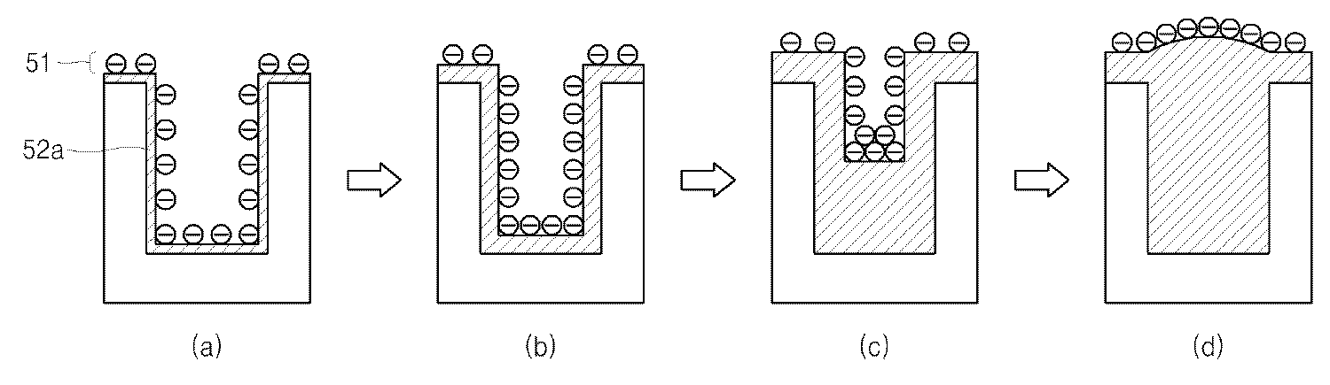
먼저 제 1 사이클에서, 제 1 전구체를 화학흡착시킨 후, 화학식 4의 화합물을 포함하는 반응 기체와 반응시키면 물질막을 형성하고자 하는 기판 표면에 전하를 띠는 원자들의 층(51)이 균일한 밀도로 형성된다(도 4의 (a) 참조). 상기 전하를 띠는 원자들은 앞서 설명한 바와 같이 할로겐족 원소들일 수 있는데, 물질막(52a)을 형성시키기 위해 중심원소들을 화학흡착시키는 데 촉매 역할을 수행한다.In the first cycle, the first precursor is chemisorbed and then reacted with a reaction gas comprising the compound of Formula 4 to form a
도 4의 (b)를 참조하면, 물질막(52a) 형성 초기에는 비아홀과 같은 리세스된 영역에 있어서 각 표면의 증착 속도가 거의 균일하지만, 전하를 띠는 원자들의 밀도의 증가 속도가 제 2 사이클이 반복됨에 따라 측벽보다 하부면에서 보다 빠르게 진행된다. 그 결과 측벽의 성장 속도보다 하부 표면의 성장 속도가 현저히 빠르게 된다.Referring to FIG. 4 (b), at the initial stage of the formation of the
그 결과 도 4의 (c)에서와 같이 보이드(void)나 씸(seam)의 형성 없이 리세스된 영역의 내부가 고루 채워지게 되고, 마침내 도 4의 (d)에서 보는 바와 같이 리세스된 영역의 내부가 결함 없이 채워지게 된다. 이와 같은 성장은 촉매 역할을 수행하는 상기 전하를 띠는 원자들의 영향이 크며, 경우에 따라서는 제 2 사이클의 반복 수행 도중에 이러한 촉매 작용을 증진시키기 위해 제 1 사이클을 수시로 수행할 수 있다.As a result, as shown in FIG. 4C, the interior of the recessed region is uniformly filled without forming a void or seam, and finally, as shown in FIG. 4D, Is filled with no defect. Such growth is highly influenced by the charged atoms that perform the catalytic function, and in some cases the first cycle may be performed from time to time to enhance such catalysis during the iterative run of the second cycle.
상기 화학식 1의 화합물은 예를 들면, 하기 화학식 5의 고리 화합물이거나, Ge(CH3)4, Ge(C2H5)4, Ge(i-C3H7)4, Ge(n-C3H7)4, Ge(i-C4H9)4, Ge(t-C4H9)4, Ge[N(CH3)2]4, Ge[NH(CH3)]4, Ge[N(CH3)(C2H5)]4, Ge[NH(C2H5)]4, Ge[N(C2H5)2]4, Ge(N(i-C3H7)2)4, Ge[N(Si(CH3)3)2]4, Si(CH3)4, Si(C2H5)4, Si(i-C3H7)4, Si(n-C3H7)4, Si(i-C4H9)4, Si(t-C4H9)4, Si[N(CH3)2]4, Si[NH(CH3)]4, Si[N(CH3)(C2H5)]4, Si[NH(C2H5)]4, Si[N(C2H5)2]4, Si(N(i-C3H7)2)4, Si[N(Si(CH3)3)2]4, Sn(CH3)4, Sn(C2H5)4, Sn(i-C3H7)4, Sn(n-C3H7)4, Sn(i-C4H9)4, Sn(t-C4H9)4, Sn[N(CH3)2]4, Sn[NH(CH3)]4, Sn[N(CH3)(C2H5)]4, Sn[NH(C2H5)]4, Sn[N(C2H5)2]4, Sn(N(i-C3H7)2)4, Sn[N(Si(CH3)3)2]4, Ga(CH3)4, Ga(C2H5)4, Ga(i-C3H7)4, Ga(n-C3H7)4, Ga(i-C4H9)4, Ga(t-C4H9)4, Ga[N(CH3)2]4, Ga[NH(CH3)]4, Ga[N(CH3)(C2H5)]4, Ga[NH(C2H5)]4, Ga[N(C2H5)2]4, Ga(N(i-C3H7)2)4, Ga[N(Si(CH3)3)2]4, In(CH3)4, In(C2H5)4, In(i-C3H7)4, In(n-C3H7)4, In(i-C4H9)4, In(t-C4H9)4, In[N(CH3)2]4, In[NH(CH3)]4, In[N(CH3)(C2H5)]4, In[NH(C2H5)]4, In[N(C2H5)2]4, In(N(i-C3H7)2)4, 또는 In[N(Si(CH3)3)2]4일 수 있다.The compound of formula (I) is, for example, to or cyclic compound of formula 5, Ge (CH 3) 4 , Ge (C 2 H 5) 4, Ge (iC 3 H 7) 4, Ge (nC 3 H 7) 4, Ge (iC 4 H 9 ) 4, Ge (tC 4 H 9) 4, Ge [N (CH 3) 2] 4, Ge [NH (CH 3)] 4, Ge [N (CH 3) (C 2 H 5)] 4, Ge [NH (C 2 H 5)] 4, Ge [N (C 2 H 5) 2] 4, Ge (N (iC 3 H 7) 2) 4, Ge [N (Si (CH 3) 3) 2] 4, Si (CH 3) 4, Si (C 2 H 5) 4, Si (iC 3 H 7) 4, Si (nC 3 H 7) 4, Si (iC 4 H 9 ) 4, Si (tC 4 H 9) 4, Si [N (CH 3) 2] 4, Si [NH (CH 3)] 4, Si [N (CH 3) (C 2 H 5)] 4, Si [NH (C 2 H 5) ] 4, Si [N (C 2 H 5) 2] 4, Si (N (iC 3 H 7) 2) 4, Si [N (Si (CH 3) 3) 2] 4, Sn (CH 3) 4 , Sn (C 2 H 5) 4, Sn (iC 3 H 7) 4, Sn (nC 3 H 7) 4, Sn (iC 4 H 9) 4, Sn (tC 4 H 9) 4, Sn [N ( CH 3) 2] 4, Sn [NH (CH 3)] 4, Sn [N (CH 3) (C 2 H 5)] 4, Sn [NH (C 2 H 5) ] 4, Sn [N (C 2 H 5) 2] 4, Sn (N (iC 3 H 7) 2) 4, Sn [N (Si (CH 3) 3) 2] 4, Ga (CH 3) 4 , Ga (C 2 H 5) 4, Ga (iC 3 H 7) 4, Ga (nC 3 H 7) 4, Ga (iC 4 H 9) 4, Ga (tC 4 H 9) 4, Ga [N ( CH 3 ) 2] 4, Ga [NH (CH 3)] 4, Ga [N (CH 3) (C 2 H 5)] 4, Ga [NH (C 2 H 5)] 4, Ga [N (C 2 H 5) 2] 4, Ga ( N (iC 3 H 7) 2) 4, Ga [N (Si (CH 3) 3) 2] 4, In (CH 3) 4, In (C 2 H 5) 4, In (iC 3 H 7) 4 , In (nC 3 H 7) 4, In (iC 4 H 9) 4, In (tC 4 H 9) 4, In [N (CH 3) 2] 4, In [NH (CH 3)] 4, In [N (CH 3) (C 2 H 5)] 4, In [NH (C 2 H 5)] 4, In [N (C 2 H 5) 2] 4, In ( N (iC 3 H 7) 2 ) 4, or In [N (Si (CH 3 ) 3) 2] may be four days.
상기 화학식 2의 화합물은 예를 들면, Sb(CH3)3, Sb[CH(CH3)2]3, Sb[N(CH3)2]3, Sb(C2H5)3, Sb(i-C3H7)3, Sb(n-C3H7)3, Sb(i-C4H9)3, Sb(t-C4H9)3, Sb(N(CH3)(C2H5))3, Sb(N(C2H5)2)3, Sb(N(i-C3H7)2)3, Sb[N(Si(CH3)3)2]3, Bi(CH3)3, Bi[CH(CH3)2]3, Bi[N(CH3)2]3, Bi(C2H5)3, Bi(i-C3H7)3, Bi(n-C3H7)3, Bi(i-C4H9)3, Bi(t-C4H9)3, Bi(N(CH3)(C2H5))3, Bi(N(C2H5)2)3, Bi(N(i-C3H7)2)3, Bi[N(Si(CH3)3)2]3, As(CH3)3, As[CH(CH3)2]3, As[N(CH3)2]3, As(C2H5)3, As(i-C3H7)3, As(n-C3H7)3, As(i-C4H9)3, As(t-C4H9)3, As(N(CH3)(C2H5))3, As(N(C2H5)2)3, As(N(i-C3H7)2)3, As[N(Si(CH3)3)2]3, Ga(CH3)3, Ga[CH(CH3)2]3, Ga[N(CH3)2]3, Ga(C2H5)3, Ga(i-C3H7)3, Ga(n-C3H7)3, Ga(i-C4H9)3, Ga(t-C4H9)3, Ga(N(CH3)(C2H5))3, Ga(N(C2H5)2)3, Ga(N(i-C3H7)2)3, Ga[N(Si(CH3)3)2]3, In(CH3)3, In[CH(CH3)2]3, In[N(CH3)2]3, In(C2H5)3, In(i-C3H7)3, In(n-C3H7)3, In(i-C4H9)3, In(t-C4H9)3, In(N(CH3)(C2H5))3, In(N(C2H5)2)3, In(N(i-C3H7)2)3, 또는 In[N(Si(CH3)3)2]3일 수 있다.The compounds of the formula 2 can be, for example, Sb (CH 3) 3, Sb [CH (CH 3) 2] 3, Sb [N (CH 3) 2] 3, Sb (C 2 H 5) 3, Sb ( iC 3 H 7) 3, Sb (nC 3 H 7) 3, Sb (iC 4 H 9) 3, Sb (tC 4 H 9) 3, Sb (N (CH 3) (C 2 H 5)) 3, Sb (N (C 2 H 5 ) 2) 3, Sb (N (iC 3 H 7) 2) 3, Sb [N (Si (CH 3) 3) 2] 3, Bi (CH 3) 3, Bi [ CH (CH 3) 2] 3 , Bi [N (CH 3) 2] 3, Bi (C 2 H 5) 3, Bi (iC 3 H 7) 3, Bi (nC 3 H 7) 3, Bi (iC 4 H 9) 3, Bi ( tC 4 H 9) 3, Bi (N (CH 3) (C 2 H 5)) 3, Bi (N (C 2 H 5) 2) 3, Bi (N (iC 3 H 7) 2) 3, Bi [N (Si (CH 3) 3) 2] 3, As (CH 3) 3, As [CH (CH 3) 2] 3, As [N (CH 3) 2] 3 , As (C 2 H 5) 3, As (iC 3 H 7) 3, As (nC 3 H 7) 3, As (iC 4 H 9) 3, As (tC 4 H 9) 3, As (N ( CH 3) (C 2 H 5 )) 3, As (N (C 2 H 5) 2) 3, As (N (iC 3 H 7) 2) 3, As [N (Si (CH 3) 3) 2 ] 3, Ga (CH 3) 3, Ga [CH (CH 3) 2] 3, Ga [N (CH 3) 2] 3, Ga (C 2 H 5) 3, Ga (iC 3 H 7) 3, Ga (nC 3 H 7) 3 , Ga (iC 4 H 9) 3, Ga (tC 4 H 9) 3, Ga (N (CH 3) (C 2 H 5)) 3, Ga (N (C 2 H 5 ) 2 ) 3 , Ga (N (iC 3 H 7 ) 2 ) 3 , Ga [N (Si (CH 3) 3) 2] 3, In (CH 3) 3, In [CH (CH 3) 2] 3, In [N (CH 3) 2] 3, In (C 2 H 5) 3, In (iC 3 H 7) 3, In (nC 3 H 7) 3, In (iC 4 H 9) 3, In (tC 4 H 9) 3, In (N (CH 3) (C 2 H 5)) 3, In ( N (C 2 H 5) 2) 3, In (N (iC 3 H 7) 2) 3, or In [N (Si (CH 3 ) 3) 2] may be 3 days .
상기 화학식 3의 화합물은 예를 들면, Te(CH3)2, Te[CH(CH3)2]2, Te[C(CH3)3]2, Te(C2H5)2, Te(n-C3H7)2, Te(i-C3H7)2, Te(t-C4H9)2, Te(i-C4H9)2, Te(CH=CH2)2, Te(CH2CH=CH2)2, Te[N(Si(CH3)3)2]2 Se(CH3)2, Se[CH(CH3)2]2, Se[C(CH3)3]2, Se(C2H5)2, Se(n-C3H7)2, Se(i-C3H7)2, Se(t-C4H9)2, Se(i-C4H9)2, Se(CH=CH2)2, Se(CH2CH=CH2)2, Se[N(Si(CH3)3)2]2일 수 있다.The compounds of the formula (3) can be, for example, Te (CH 3) 2, Te [CH (CH 3) 2] 2, Te [C (CH 3) 3] 2, Te (C 2 H 5) 2, Te ( nC 3 H 7) 2, Te (iC 3 H 7) 2, Te (tC 4 H 9) 2, Te (iC 4 H 9) 2, Te (CH = CH 2) 2, Te (CH 2 CH = CH 2) 2, Te [N ( Si (CH 3) 3) 2] 2 Se (CH 3) 2, Se [CH (CH 3) 2] 2, Se [C (CH 3) 3] 2, Se (C 2 H 5) 2, Se ( nC 3 H 7) 2, Se (iC 3 H 7) 2, Se (tC 4 H 9) 2, Se (iC 4 H 9) 2, Se (CH = CH 2) 2 , Se (CH 2 CH = CH 2) 2, Se [N (Si (CH 3) 3) 2] may be two days.
그러나, 화학식 1 내지 3의 화합물은 위에 기재한 것에 한정되는 것은 아니다.However, the compounds of the formulas (1) to (3) are not limited to those described above.
<화학식 5>≪ Formula 5 >

상기 화학식 4의 화합물은 예를 들면 CH3F, CH3Cl, CH3Br, CH3I, HF, HCl, HBr, HI, F2, Cl2, Br2, I2 등 일 수 있으며 여기에 한정되는 것은 아니다.Here a compound of formula (4), for example, CH 3 F, CH 3 Cl, CH 3 Br, CH 3 I, be HF, HCl, HBr, HI, F 2, Cl 2, Br 2, I 2 , etc., and But is not limited thereto.
앞서 설명한 바와 같이 상기 제 1 전구체의 중심원소는 상기 제 2 전구체의 중심원소와 상이하며, 특히, 상기 제 1 전구체의 중심원소의 족번호는 상기 제 2 전구체의 중심원소의 족번호와 서로 상이할 수 있다. 그 결과 증착되는 물질막은, 예를 들면, GeTe, SbTe, 또는 InSe일 수 있다.As described above, the central element of the first precursor is different from the central element of the second precursor. Particularly, the group number of the central element of the first precursor is different from the group number of the central element of the second precursor . As a result, the material film to be deposited may be, for example, GeTe, SbTe, or InSe.
선택적으로, 상기 화학흡착시 챔버 내에는 C2H2, NH3, SiH4, 및 O2로 이루어지 는 군으로부터 선택되는 기체가 적어도 1종 이상 존재할 수 있다. 이와 같이 하는 경우 물질막 내에 C, N, Si, O 등의 원소들을 도핑하는 효과를 가져올 수 있다.Alternatively, at least one gas selected from the group consisting of C 2 H 2 , NH 3 , SiH 4 , and O 2 may be present in the chamber during the chemical adsorption. In this case, the effect of doping elements such as C, N, Si and O into the material film can be obtained.
선택적으로, 상기 제 1 사이클은 화학흡착된 상기 제 1 전구체의 중심원소와 상기 화학식 4의 화합물을 포함하는 반응기체를 반응시키는 단계 이후에, 상기 화학식 1 내지 3 중의 어느 한 화합물을 제 3 전구체로 이용하여 상기 제 3 전구체의 중심원소를 화학흡착시키는 단계를 더 포함할 수 있다.Alternatively, the first cycle may comprise reacting any of the compounds of Formulas 1 to 3 as a third precursor after reacting the chemically adsorbed reactant gas comprising the central element of the first precursor and the compound of Formula 4 And chemically adsorbing the central element of the third precursor using the first precursor.
또, 선택적으로, 상기 제 2 사이클도 상기 화학식 1 내지 3 중의 어느 한 화합물을 제 3 전구체로 이용하여 상기 제 3 전구체의 중심원소를 화학흡착시키는 단계를 더 포함할 수 있다.Alternatively, the second cycle may further include the step of chemically adsorbing the central element of the third precursor by using any one of the compounds of Formulas 1 to 3 as the third precursor.
상기 제 1 사이클 및 상기 제 2 사이클이 상기 제 3 전구체의 중심원소를 화학흡착시키는 단계를 더 포함하는 경우에는 제 3 전구체를 공급하여 제 3 전구체의 중심원소를 화학흡착시키고 퍼징기체를 공급함으로써 아직 흡착되지 않은 제 3 전구체와 물리흡착을 하고 있는 중심원자들을 반응챔버로부터 제거할 수 있다. 특히, 제 3 전구체를 공급하는 방법/조건 및 퍼징 기체를 공급하는 방법/및 조건은 다른 전구체들 및 퍼징 기체의 공급 방법/조건과 유사하게 수행될 수 있다.If the first cycle and the second cycle further comprise chemically adsorbing the central element of the third precursor, the third precursor is supplied to chemisorb the central element of the third precursor and supply the purging gas The central atoms that are physically adsorbed with the unadsorbed third precursor can be removed from the reaction chamber. In particular, the method / condition for supplying the third precursor and the method / condition for supplying the purge gas may be performed similar to the feed method / condition of the other precursors and the purge gas.
상기 제 3 전구체의 중심원소는 상기 제 1 전구체의 중심원소와 상이할 수 있다. 또, 상기 제 3 전구체의 중심원소는 상기 제 2 전구체의 중심원소와 상이할 수 있다. 선택적으로, 상기 제 3 전구체의 중심원소는 상기 제 1 전구체의 중심원소와 상이하고, 아울러 상기 제 2 전구체의 중심원소와도 상이할 수 있다. 선택적으로, 상기 제 1 전구체 내지 제 3 전구체의 각 중심원소의 족번호가 모두 상이할 수 있다.The central element of the third precursor may be different from the central element of the first precursor. In addition, the central element of the third precursor may be different from the central element of the second precursor. Alternatively, the central element of the third precursor may be different from the central element of the first precursor, and may also be different from the central element of the second precursor. Alternatively, the group numbers of the respective central elements of the first precursor to the third precursor may be different from each other.
이와 같이 제 1 전구체 내지 제 3 전구체를 이용함으로써 얻어지는 물질막은, 예를 들면, GeSbTe, GeTeAs, SbTeSn, SeTeSn, GeTeSe, SbSeBi, GeBiTe, GeTeTi, GaTeSe, 및 InSbTe로 이루어지는 군으로부터 선택되는 어느 하나일 수 있다.The material film obtained by using the first to third precursors may be any one selected from the group consisting of GeSbTe, GeTeAs, SbTeSn, SeTeSn, GeTeSe, SbSeBi, GeBiTe, GeTeTi, GaTeSe, and InSbTe have.
물질막의 형성 방법 IIMethod of forming a material film II
본 발명의 물질막을 형성하는 방법의 다른 구현예는 제 1 사이클과 제 2 사이클로 이루어져 있을 수 있다.Another embodiment of the method of forming a material film of the present invention may consist of a first cycle and a second cycle.
상기 제 1 사이클은 물질막을 형성하는 동안 1회만 수행될 수도 있고, 연속적으로 또는 불연속적으로 2회 내지 10회 수행될 수도 있다. 상기 제 1 사이클은 하기 화학식 6 내지 8 중의 어느 한 화합물을 제 1 전구체로 이용하여 상기 제 1 전구체의 중심원소를 기판 표면에 화학흡착시키는 단계, 화학흡착된 상기 제 1 전구체의 중심원소와 하기 화학식 4의 화합물을 포함하는 반응기체를 반응시키는 단계, 상기 제 1 전구체의 중심원소와 상이한 중심원소를 갖는 하기 화학식 6 내지 8 중의 어느 한 화합물을 제 2 전구체로 이용하여 상기 제 2 전구체의 중심원소를 화학흡착시키는 단계, 및 상기 제 1 전구체의 중심원소 및 상기 제 2 전구체의 중심원소와 상이한 중심원소를 갖는 하기 화학식 6 내지 8 중의 어느 한 화합물을 제 3 전구체로 이용하여 상기 제 3 전구체의 중심원소를 화학흡착시키는 단계를 포함할 수 있다.The first cycle may be performed only once during formation of the material film, and may be performed continuously or discontinuously two to ten times. Chemically adsorbing the central element of the first precursor to the surface of the substrate using the compound of any one of Chemical Formulas 6 to 8 as a first precursor, Reacting a reaction gas containing a compound of the formula (4) and a compound of the following formula (6) to (8) having a central element different from the central element of the first precursor as a second precursor, Chemically adsorbing the first precursor and a compound having a central element different from the central element of the first precursor and a central element different from the central element of the first precursor as a third precursor, And then chemically adsorbing it.
<화학식 6>(6)
M4R10R11R12R13 M 4 R 10 R 11 R 12 R 13
<화학식 7>≪ Formula 7 >
M5R14R15R16 M 5 R 14 R 15 R 16
<화학식 8>(8)
M6R17R18 M 6 R 17 R 18
(상기 화학식 6 내지 8에서 중심원소 M4는 Pb, Ti, Zr 중의 어느 하나이고, 중심원소 M5는 Bi, Nb, Ta, La 중의 어느 하나이고, 중심원소 M6는 Sr 또는 Ba이고,Wherein the central element M 4 is any one of Pb, Ti and Zr, the central element M 5 is any one of Bi, Nb, Ta and La, the central element M 6 is Sr or Ba,
R10 내지 R18은 각각 독립적으로 메틸기 또는 탄소수 2 내지 5의 분지형 탄화수소 사슬로서 주쇄 내에 O, N, S, P, Si, Te, Sb, Se, Sn, Bi, In 중의 어느 하나 이상을 포함할 수 있고 상기 분지형 탄화수소 사슬의 수소원자는 치환되지 않거나 탄소수 1 내지 10의 알킬기, 탄소수 3 내지 10의 알릴기(allyl group), 탄소수 2 내지 10의 비닐기, 아민기, 할로겐기, 시안기, 및 탄소수 6 내지 10의 아릴기(aryl group)로 이루어지는 군으로부터 선택되는 어느 하나로 치환될 수 있고, 또는 R10 내지 R13의 어느 둘, R14 내지 R16의 어느 둘, 또는 R17 및 R18은 주쇄 또는 측쇄가 직접 또는 탄소수 2 내지 6의 하이드로카빌렌 라디칼에 의하여 상호 연결됨으로써 호모 또는 헤테로 고리형 탄화수소를 이룰 수 있음)R 10 to R 18 each independently represents a methyl group or a branched hydrocarbon chain having 2 to 5 carbon atoms and contains at least one of O, N, S, P, Si, Te, Sb, Se, Sn, And the hydrogen atom of the branched hydrocarbon chain may be an unsubstituted or alkyl group having 1 to 10 carbon atoms, an allyl group having 3 to 10 carbon atoms, a vinyl group having 2 to 10 carbon atoms, an amine group, a halogen group, a cyano group , And an aryl group having 6 to 10 carbon atoms, or any two of R 10 to R 13 , any two of R 14 to R 16 , or R 17 and R 18 may form a homo or heterocyclic hydrocarbon by connecting the main chain or side chain directly or via a hydrocarbylene radical having 2 to 6 carbon atoms)
<화학식 4>≪ Formula 4 >
R-XR-X
(상기 화학식 4에서 X 및 R은 위에서 정의한 바와 동일함)(X and R in Formula 4 are the same as defined above)
상기 제 2 사이클은 물질막을 형성하는 동안 여러 차례 반복될 수 있다. 통상 상기 제 2 사이클은 30회 내지 200회 반복될 수 있다. 상기 제 2 사이클은 상기 제 1 전구체를 이용하여 상기 제 1 전구체의 중심원소를 화학흡착시키는 단계, 상기 제 2 전구체를 이용하여 상기 제 2 전구체의 중심원소를 화학증착시키는 단계, 및 상기 제 3 전구체를 이용하여 상기 제 3 전구체의 중심원소를 화학흡착시키는 단계를 포함할 수 있다.The second cycle may be repeated several times during formation of the material film. Typically, the second cycle may be repeated 30 to 200 times. Chemically adsorbing a central element of the first precursor using the first precursor; chemically depositing a center element of the second precursor using the second precursor; To chemisorb the central element of the third precursor.
상기 제 1 사이클에서 제 1 전구체의 중심원소가 화학흡착되는 "기판 표면"은 앞서 언급한 반도체 단위 소자들이 형성된 기판 및/또는 절연막의 표면일 수도 있고, 제 1 사이클 및/또는 제 2 사이클의 반복에 따라 형성된 물질막의 일부의 표면일 수도 있다. The "substrate surface" on which the central element of the first precursor is chemically adsorbed in the first cycle may be the surface of the substrate and / or the insulating film on which the above-mentioned semiconductor unit elements are formed and may be a repetition of the first cycle and / May be the surface of a part of the material film formed according to < RTI ID = 0.0 >
이하에서는 상기 제 1 사이클을 더욱 상세하게 설명한다. 상기 제 1 사이클은 원자층 증착 방법을 예로 들어 설명하지만 원자층 증착 방법에 한정되는 것은 아니다. 상기 제 1 사이클의 기체 펄싱 다이아그램을 도 5에 나타내었다.Hereinafter, the first cycle will be described in more detail. The first cycle is described by taking the atomic layer deposition method as an example, but it is not limited to the atomic layer deposition method. The gas pulsing diagram of the first cycle is shown in Fig.
도 5를 참조하면, 제 1 전구체를 T1 시간 동안 약 1 torr 내지 약 10 torr의 압력으로 반응 챔버 내로 주입할 수 있다. 상기 T1 시간은 약 0.5 초 내지 약 10 초 일 수 있다. 상기 반응 챔버는 약 200 ℃ 내지 약 400 ℃의 온도를 가질 수 있다. 상기 반응 챔버의 온도에 의하여 상기 제 1 전구체의 중심 원자에 결합된 작용기들은 중심 원자와 분리되고, 상기 중심 원자는 기판의 표면에 부착된다. 상기 기판과 직접 결합한 중심 원자들은 화학 흡착을 하는 반면, 상기 기판과 직접 결합하 지 않는 중심 원자들은 물리 흡착을 하게 된다.Referring to Figure 5, the first precursor may be injected into the reaction chamber at a pressure of about 1 torr to about 10 torr for a period of time Tl. The T1 time may be about 0.5 seconds to about 10 seconds. The reaction chamber may have a temperature of about 200 < 0 > C to about 400 < 0 > C. By the temperature of the reaction chamber, the functional groups bonded to the central atom of the first precursor are separated from the central atom, and the central atom is attached to the surface of the substrate. The central atoms directly bonded to the substrate undergo chemisorption, while the central atoms that do not bond directly to the substrate undergo physical adsorption.
그 후, 상기 제 1 전구체의 공급을 차단하고 T2 시간 동안 퍼징 기체를 공급함으로써 아직 흡착되지 않은 제 1 전구체와 물리흡착을 하고 있는 중심 원자들을 반응 챔버로부터 제거한다. 상기 퍼징 기체로는 불활성 가스로서 아르곤(Ar), 헬륨(He) 또는 질소(N2) 또는 수소(H2)가 이용될 수 있다.Thereafter, the supply of the first precursor is blocked and the purging gas is supplied for T2 hours to remove the central atoms from the reaction chamber that are physically adsorbing the first precursor that has not yet been adsorbed. As the purging gas, argon (Ar), helium (He), nitrogen (N 2 ), or hydrogen (H 2 ) may be used as an inert gas.
다음으로 T3 시간 동안 상기 화학식 4의 반응 기체를 약 1 torr 내지 약 10 torr의 압력으로 반응 챔버 내로 주입할 수 있다. 상기 T3 시간은 약 0.5 초 내지 약 10 초 일 수 있다. 상기 반응 챔버는 약 200 ℃ 내지 약 400 ℃의 온도를 가질 수 있다. 상기 반응 기체는 표면에 화학흡착되어 있는, 제 1 전구체의 중심 원소와 반응하게 되고 상기 반응에 의하여 기판의 표면은 음 전하를 띠게 된다.The reactive gas of Formula 4 may then be injected into the reaction chamber at a pressure of about 1 torr to about 10 torr for a time T3. The T3 time may be from about 0.5 seconds to about 10 seconds. The reaction chamber may have a temperature of about 200 < 0 > C to about 400 < 0 > C. The reactive gas reacts with the central element of the first precursor chemically adsorbed on the surface, and the surface of the substrate becomes negative by the reaction.
이어서 상기 퍼징 기체의 공급 단계와 마찬가지로 T4 시간 동안 퍼징 기체를 공급하여 반응 챔버 내의 불필요한 기체들을 제거할 수 있다.Subsequently, as in the supplying step of the purge gas, the purge gas may be supplied for T4 hours to remove unnecessary gases in the reaction chamber.
그런 후, 제 2 전구체를 T5 시간 동안 약 1 torr 내지 약 10 torr의 압력으로 반응 챔버 내로 주입할 수 있다. 상기 T5 시간은 약 0.5 초 내지 약 10 초 일 수 있다. 상기 반응 챔버는 약 200 ℃ 내지 약 400 ℃의 온도를 가질 수 있다. 상기 반응 챔버의 온도에 의하여 상기 제 2 전구체의 중심 원자에 결합된 작용기들은 중심 원자와 분리되고, 상기 중심 원자는 기판의 표면에 부착된다. 상기 기판과 직접 결합한 중심 원자들은 화학 흡착을 하는 반면, 상기 기판과 직접 결합하지 않는 중심 원자들은 물리 흡착을 하게 된다.The second precursor can then be injected into the reaction chamber at a pressure of about 1 torr to about 10 torr for T5. The T5 time may be about 0.5 seconds to about 10 seconds. The reaction chamber may have a temperature of about 200 < 0 > C to about 400 < 0 > C. By the temperature of the reaction chamber, the functional groups bonded to the central atom of the second precursor are separated from the central atom, and the central atom is attached to the surface of the substrate. The central atoms directly bonded to the substrate undergo chemisorption, while the central atoms that do not bond directly to the substrate undergo physical adsorption.
이어서 상기 퍼징 기체의 공급 단계와 마찬가지로 T6 시간 동안 퍼징 기체를 공급하여 반응 챔버 내의 불필요한 기체들을 제거할 수 있다.Subsequently, as in the supplying of the purge gas, purging gas may be supplied for T6 hours to remove unnecessary gases in the reaction chamber.
그런 후, 제 3 전구체를 T7 시간 동안 약 1 torr 내지 약 10 torr의 압력으로 반응 챔버 내로 주입할 수 있다. 상기 T7 시간은 약 0.5 초 내지 약 10 초 일 수 있다. 상기 반응 챔버는 약 200 ℃ 내지 약 400 ℃의 온도를 가질 수 있다. 상기 반응 챔버의 온도에 의하여 상기 제 2 전구체의 중심 원자에 결합된 작용기들은 중심 원자와 분리되고, 상기 중심 원자는 기판의 표면에 부착된다. 상기 기판과 직접 결합한 중심 원자들은 화학 흡착을 하는 반면, 상기 기판과 직접 결합하지 않는 중심 원자들은 물리 흡착을 하게 된다.The third precursor can then be injected into the reaction chamber at a pressure of about 1 torr to about 10 torr for T7 hours. The T7 time may be about 0.5 seconds to about 10 seconds. The reaction chamber may have a temperature of about 200 < 0 > C to about 400 < 0 > C. By the temperature of the reaction chamber, the functional groups bonded to the central atom of the second precursor are separated from the central atom, and the central atom is attached to the surface of the substrate. The central atoms directly bonded to the substrate undergo chemisorption, while the central atoms that do not bond directly to the substrate undergo physical adsorption.
제 1 사이클의 마지막 단계로서, T8 시간 동안 퍼징 기체를 공급하여 반응 챔버 내의 불필요한 기체들을, 예를 들면 아직 흡착되지 않은 제 1 전구체와 물리흡착을 하고 있는 중심 원자들을 반응 챔버로부터 제거할 수 있다.As the last step of the first cycle, purging gas may be supplied for T8 hours to remove the unnecessary gases in the reaction chamber, for example the central atoms physically adsorbing the first precursor that have not yet been adsorbed, from the reaction chamber.
이상의 단계들로 이루어지는 제 1 사이클은 물질막을 형성하기 위한 최초 사이클이며, 물질막이 형성되는 동안 1회만 수행될 수도 있지만, 선택적으로 2회 내지 10회 반복 수행할 수도 있다. 상기 제 1 사이클의 반복 수행은 연속적으로 이루어질 수도 있고, 후술하는 제 2 사이클의 반복 수행 사이에 수시로 개재될 수도 있다.The first cycle consisting of the above steps is the first cycle for forming the material film, and may be performed only once during the formation of the material film, but may alternatively be performed two to ten times. The repetitive execution of the first cycle may be continuous or intermittently interposed between the repetition of the second cycle described later.
상기 제 1 전구체, 제 2 전구체, 제 3 전구체 및 반응 기체는 반응 챔버의 크기에 따라 10 내지 1000 sccm의 양으로 0.5초 내지 60초 동안 주입될 수 있다.The first precursor, the second precursor, the third precursor, and the reactive gas may be injected for 0.5 to 60 seconds in an amount of 10 to 1000 sccm, depending on the size of the reaction chamber.
이하에서는 상기 제 2 사이클을 상세하게 설명한다. 상기 제 2 사이클도 원 자층 증착 방법을 예로 들어 설명하지만 원자층 증착 방법에 한정되는 것은 아니다. 상기 제 2 사이클의 기체 펄싱 다이아그램을 도 6에 나타내었다.Hereinafter, the second cycle will be described in detail. The second cycle will be described by taking the atomic layer deposition method as an example, but it is not limited to the atomic layer deposition method. The gas pulsing diagram of the second cycle is shown in Fig.
도 6을 참조하면, 제 1 전구체를 T1 시간 동안 약 1 torr 내지 약 10 torr의 압력으로 반응 챔버 내로 주입할 수 있다. 상기 T1 시간은 약 0.5 초 내지 약 10 초 일 수 있다. 상기 반응 챔버는 약 200 ℃ 내지 약 400 ℃의 온도를 가질 수 있다. 상기 반응 챔버의 온도에 의하여 상기 제 1 전구체의 중심 원자에 결합된 작용기들은 중심 원자와 분리되고, 상기 중심 원자는 기판의 표면에 부착된다. 상기 기판과 직접 결합한 중심 원자들은 화학 흡착을 하는 반면, 상기 기판과 직접 결합하지 않는 중심 원자들은 물리 흡착을 하게 된다. 앞서 설명한 바와 같이 여기서 말하는 기판은 반도체 단위 소자들이 형성된 기판 및/또는 절연막일 수도 있고, 제 1 사이클 및/또는 제 2 사이클의 반복에 따라 형성된 물질막의 일부일 수도 있다.Referring to FIG. 6, the first precursor may be injected into the reaction chamber at a pressure of about 1 torr to about 10 torr for a period of time Tl. The T1 time may be about 0.5 seconds to about 10 seconds. The reaction chamber may have a temperature of about 200 < 0 > C to about 400 < 0 > C. By the temperature of the reaction chamber, the functional groups bonded to the central atom of the first precursor are separated from the central atom, and the central atom is attached to the surface of the substrate. The central atoms directly bonded to the substrate undergo chemisorption, while the central atoms that do not bond directly to the substrate undergo physical adsorption. As described above, the substrate referred to herein may be a substrate and / or an insulating film on which semiconductor unit elements are formed and may be a part of a material film formed according to the repetition of the first cycle and / or the second cycle.
그 후, 상기 제 1 전구체의 공급을 차단하고 T2 시간 동안 퍼징 기체를 공급함으로써 아직 흡착되지 않은 제 1 전구체와 물리흡착을 하고 있는 중심 원자들을 반응 챔버로부터 제거한다. 상기 퍼징 기체로는 불활성 가스로서 아르곤(Ar), 헬륨(He) 또는 질소(N2) 또는 수소(H2)가 이용될 수 있다.Thereafter, the supply of the first precursor is blocked and the purging gas is supplied for T2 hours to remove the central atoms from the reaction chamber that are physically adsorbing the first precursor that has not yet been adsorbed. As the purging gas, argon (Ar), helium (He), nitrogen (N 2 ), or hydrogen (H 2 ) may be used as an inert gas.
다음으로 제 2 전구체를 T3 시간 동안 약 1 torr 내지 약 10 torr의 압력으로 반응 챔버 내로 주입할 수 있다. 상기 T3 시간은 약 0.5 초 내지 약 10 초 일 수 있다. 상기 반응 챔버는 약 200 ℃ 내지 약 400 ℃의 온도를 가질 수 있다. 상기 반응 챔버의 온도에 의하여 상기 제 2 전구체의 중심 원자에 결합된 작용기들은 중심 원자와 분리되고, 상기 중심 원자는 기판의 표면에 부착된다. 상기 기판과 직접 결합한 중심 원자들은 화학 흡착을 하는 반면, 상기 기판과 직접 결합하지 않는 중심 원자들은 물리 흡착을 하게 된다.The second precursor can then be injected into the reaction chamber at a pressure of from about 1 torr to about 10 torr for a period of T3. The T3 time may be from about 0.5 seconds to about 10 seconds. The reaction chamber may have a temperature of about 200 < 0 > C to about 400 < 0 > C. By the temperature of the reaction chamber, the functional groups bonded to the central atom of the second precursor are separated from the central atom, and the central atom is attached to the surface of the substrate. The central atoms directly bonded to the substrate undergo chemisorption, while the central atoms that do not bond directly to the substrate undergo physical adsorption.
이어서 상기 퍼징 기체의 공급 단계와 마찬가지로 T4 시간 동안 퍼징 기체를 공급하여 반응 챔버 내의 불필요한 기체들을 제거할 수 있다.Subsequently, as in the supplying step of the purge gas, the purge gas may be supplied for T4 hours to remove unnecessary gases in the reaction chamber.
다음으로 제 3 전구체를 상기 제 2 전구체와 동일한 방법으로 주입하여 T5 시간 동안 제 2 전구체의 중심 원자를 화학흡착시킨다.The third precursor is then injected in the same manner as the second precursor to chemisorb the central atom of the second precursor for T5 hours.
제 2 사이클의 마지막 단계로서, T6 시간 동안 퍼징 기체를 공급하여 반응 챔버 내의 불필요한 기체들을, 예를 들면 아직 흡착되지 않은 제 3 전구체와 물리흡착을 하고 있는 제 3 전구체의 중심 원자들을 반응 챔버로부터 제거할 수 있다.As the last step of the second cycle, purging gas is supplied for T6 hours to remove unnecessary gases in the reaction chamber from the reaction chamber, for example, the center atoms of the third precursor physically adsorbing the third precursor not yet adsorbed can do.
이와 같은 제 1 사이클 및/또는 제 2 사이클의 반복 수행을 통해 형성되는 물질막의 형성 메커니즘은 상기 "물질막의 형성 방법 I"에서 살펴본 바와 동일하므로 여기서는 생략한다.The formation mechanism of the material film formed through repetition of the first cycle and / or the second cycle is the same as that described in the "Method I of forming a material film"
상기 화학식 4의 화합물은 예를 들면 CH3F, CH3Cl, CH3Br, CH3I, HF, HCl, HBr, HI, F2, Cl2, Br2, I2 등일 수 있으며 여기에 한정되는 것은 아니다.The compounds of the general formula (4), for example, CH 3 F, CH 3 Cl, CH 3 Br, CH 3 I, HF, HCl, HBr, HI, F 2, Cl 2, Br 2, I 2 or the like are limited to It is not.
상기 화학식 6의 화합물은 예를 들면, 하기 화학식 7 내지 화학식 13 중의 어느 한 화합물일 수 있다. 또는, 이들 화합물 외에 Pb(TMHD)2, Pb(TMHD)2-PMDT (여기서, PMDT는 펜타메틸디에틸렌트리아민임), Pb(METHD)2 (여기서, METHD는 메톡 시에톡시테트라메틸헵탄디오네이트임), Zr(DMAE)4, Zr(METHD)4, Zr(MPD)(METHD)2, Zr[N(CH3)2]4, Zr[N(C2H5)2]4, Zr(O-t-C4H9)4, Zr(O-i-CH3)4, Zr(O-i-C2H5)4, Zr(O-i-C3H7)4, Ti(MPD)(METHD)2, Ti(DMAE)4, Ti[N(C2H5)2]4, Ti(O-t-C4H9)4, Ti(O-i-CH3)4, Ti(O-i-C2H5)4, Ti(O-i-C3H7)4 등일 수 있으며 여기에 한정되는 것은 아니다.The compound of formula (6) may be, for example, any one of the following formulas (7) to (13). Alternatively, in addition to these compounds, Pb (TMHD) 2 , Pb (TMHD) 2- PMDT (where PMDT is pentamethyldiethylenetriamine), Pb (METHD) 2 (where METHD is methoxyethoxytetramethylheptanedio Nate Im), Zr (DMAE) 4, Zr (METHD) 4, Zr (MPD) (METHD) 2, Zr [N (CH 3) 2] 4, Zr [N (C 2 H 5) 2] 4, Zr (O- t -C 4 H 9) 4, Zr (O- i -CH 3) 4, Zr (O- i -C 2 H 5) 4, Zr (O- i -C 3 H 7) 4, Ti (MPD) (METHD) 2, Ti (DMAE) 4, Ti [N (C 2 H 5) 2] 4, Ti (O- t -C 4 H 9) 4, Ti (O- i -CH 3) 4 , Ti (O - i - C 2 H 5 ) 4 , Ti (O - i - C 3 H 7 ) 4 , and the like.
<화학식 7>≪ Formula 7 >

<화학식 8>(8)

<화학식 9>≪ Formula 9 >

<화학식 10>≪

<화학식 11>≪ Formula 11 >

<화학식 12>≪ Formula 12 >

<화학식 13>≪ Formula 13 >

상기 화학식 7의 화합물은 Bi(CH3)3, Bi(C6H5)3, Bi(TMHD)3, La(TMHD)3, Ta(i-OPr)5, Ta(i-OPr)4(TMHD), Ta(i-OPr)4(DMAE), 또는 Ta(DMAE)5 등일 수 있으며 여기에 한정되는 것은 아니다.The compound of Formula 7 is Bi (CH 3) 3, Bi (C 6 H 5) 3, Bi (TMHD) 3, La (TMHD) 3, Ta (i-OPr) 5, Ta (i-OPr) 4 ( TMHD), Ta (i-OPr) 4 (DMAE), Ta (DMAE) 5 , and the like.
상기 화학식 8의 화합물은 Ba(TMHD)2, Ba(AcAc)2, Ba(MEP)2 (Ba(di(methoxyethoxy)-propanol)2), Ba(MPMP)2 (Ba(methoxypropylaminomethoxyethoxypropanol)2), Ba(METHD)2, Sr(TMHD)2, Sr(AcAc)2, Sr(MEP)2, Sr(MPMP)2, 또는 Sr(METHD)2 등일 수 있으며 여기에 한정되는 것은 아니다.The compound of Formula 8 is a Ba (TMHD) 2, Ba ( AcAc) 2, Ba (MEP) 2 (Ba (di (methoxyethoxy) -propanol) 2), Ba (MPMP) 2 (Ba (methoxypropylaminomethoxyethoxypropanol) 2), Ba (METHD) 2 , Sr (TMHD) 2 , Sr (AcAc) 2 , Sr (MEP) 2 , Sr (MPMP) 2 , or Sr (METHD) 2 .
상기 제 1 전구체, 제 2 전구체 및 제 3 전구체의 중심원소는 모두 서로 상이할 수 있다. 또한, 상기 화학흡착시 챔버 내에는 산소(O2), 오존(O3), 이산화질소(NO2), 또는 산화이질소(N2O) 등과 같이 산소를 포함하는 가스를 함께 공급하거나 이미 공급되어 존재할 수 있다.The central elements of the first precursor, the second precursor, and the third precursor may be different from each other. When the chemical adsorption is performed, a gas containing oxygen such as oxygen (O 2 ), ozone (O 3 ), nitrogen dioxide (NO 2 ), or nitrogen oxide (N 2 O) .
상기 제 1 전구체, 제 2 전구체 및 제 3 전구체를 이용하여 형성되는 물질막은, 예를 들면, PZT (Pb(Zr, Ti)O3), SBT (SrBi2Ta2O3), BLT (Bi(La, Ti)O3), PLZT (Pb(La, Zr)TiO3), PNZT (Pb(Nb, Zr, Ti)O3), BFO (BiFeO3) 또는 BST (Ba(Sr, Ti)O3) 물질막일 수 있다. 그러나, 이들 물질막에 한정되는 것은 아니다.The material film formed by using the first precursor, the second precursor and the third precursor may be formed of a material selected from the group consisting of PZT (Pb (Zr, Ti) O 3 ), SBT (SrBi 2 Ta 2 O 3 ), BLT La, Ti) O 3), PLZT (Pb (La, Zr) TiO 3), PNZT (Pb (Nb, Zr, Ti) O 3), BFO (BiFeO 3) or BST (Ba (Sr, Ti) O 3 ) Material film. However, the present invention is not limited to these material films.
물질막의Material film 형성 방법 How to form IIIIII
본 발명의 물질막을 형성하는 방법의 또 다른 구현예는 제 1 사이클과 제 2 사이클로 이루어져 있을 수 있다.Another embodiment of the method of forming a material film of the present invention may consist of a first cycle and a second cycle.
상기 제 1 사이클은 물질막을 형성하는 동안 1회만 수행될 수도 있고, 연속적으로 또는 불연속적으로 2회 내지 10회 수행될 수도 있다. 상기 제 1 사이클은 Fe 전구체, Co 전구체, Ni 전구체, Mn 전구체, Pt 전구체 중의 어느 한 화합물을 제 1 전구체로 이용하여 상기 제 1 전구체의 중심원소를 기판 표면에 화학흡착시키는 단계, 화학흡착된 상기 제 1 전구체의 중심원소와 하기 화학식 4의 화합물을 포함하는 반응기체를 반응시키는 단계, 및 Fe 전구체, Co 전구체, Ni 전구체, Mn 전구체, Pt 전구체 중의 어느 한 화합물로서 상기 제 1 전구체의 중심원소와 상이한 중심원소를 갖는 화합물을 제 2 전구체로 이용하여 상기 제 2 전구체의 중심원소를 화학흡착시키는 단계를 포함할 수 있다.The first cycle may be performed only once during formation of the material film, and may be performed continuously or discontinuously two to ten times. Chemically adsorbing the central element of the first precursor on the surface of the substrate by using any one of an Fe precursor, a Co precursor, a Ni precursor, a Mn precursor, and a Pt precursor as a first precursor, Reacting a reaction gas comprising a central element of the first precursor and a compound represented by the following formula 4 as a precursor and a precursor of a precursor such as a Fe precursor, a Ni precursor, a Mn precursor, and a Pt precursor, And chemisorbing the central element of the second precursor using a compound having a different central element as a second precursor.
<화학식 4>≪ Formula 4 >
R-XR-X
(상기 화학식 4에서 X 및 R은 위에서 정의한 바와 동일함)(X and R in Formula 4 are the same as defined above)
상기 제 2 사이클은 물질막을 형성하는 동안 여러 차례 반복될 수 있다. 통상 상기 제 2 사이클은 30회 내지 200회 반복될 수 있다. 상기 제 2 사이클은 상기 제 1 전구체를 이용하여 상기 제 1 전구체의 중심원소를 화학흡착시키는 단계, 및 상기 제 2 전구체를 이용하여 상기 제 2 전구체의 중심원소를 화학흡착시키는 단계를 포함할 수 있다.The second cycle may be repeated several times during formation of the material film. Typically, the second cycle may be repeated 30 to 200 times. The second cycle may include chemisorbing the central element of the first precursor using the first precursor and chemisorbing the central element of the second precursor using the second precursor .
상기 제 1 사이클에서 제 1 전구체의 중심원소가 화학흡착되는 "기판 표면"은 앞서 언급한 반도체 단위 소자들이 형성된 기판 및/또는 절연막의 표면일 수도 있고, 제 1 사이클 및/또는 제 2 사이클의 반복에 따라 형성된 물질막의 일부의 표면일 수도 있다. The "substrate surface" on which the central element of the first precursor is chemically adsorbed in the first cycle may be the surface of the substrate and / or the insulating film on which the above-mentioned semiconductor unit elements are formed and may be a repetition of the first cycle and / May be the surface of a part of the material film formed according to < RTI ID = 0.0 >
상기 제 1 사이클 및 제 2 사이클은 앞서 설명한 "물질막의 형성 방법 I"에서 설명한 바와 동일한 방법으로 수행될 수 있다. 따라서, 여기서는 상세한 설명을 생략한다.The first cycle and the second cycle may be performed in the same manner as described above in "Method I of forming a material film ". Therefore, detailed description is omitted here.
선택적으로, 상기 제 1 사이클은 화학흡착된 상기 제 1 전구체의 중심원소와 상기 화학식 4의 화합물을 포함하는 반응기체를 반응시키는 단계 이후에, 상기 화학식 1 내지 3 중의 어느 한 화합물을 제 3 전구체로 이용하여 상기 제 3 전구체의 중심원소를 화학흡착시키는 단계를 더 포함할 수 있다.Alternatively, the first cycle may comprise reacting any of the compounds of Formulas 1 to 3 as a third precursor after reacting the chemically adsorbed reactant gas comprising the central element of the first precursor and the compound of Formula 4 And chemically adsorbing the central element of the third precursor using the first precursor.
또, 선택적으로, 상기 제 2 사이클도 상기 화학식 1 내지 3 중의 어느 한 화합물을 제 3 전구체로 이용하여 상기 제 3 전구체의 중심원소를 화학흡착시키는 단계를 더 포함할 수 있다.Alternatively, the second cycle may further include the step of chemically adsorbing the central element of the third precursor by using any one of the compounds of Formulas 1 to 3 as the third precursor.
이 때, 제 1 전구체, 제 2 전구체 및 제 3 전구체를 이용하는 경우는 앞서 설명한 "물질막의 형성 방법 I" 및 "물질막의 형성 방법 II"에서 설명한 바와 동일한 방법으로 수행될 수 있으므로 여기서는 상세한 설명을 생략한다.In this case, the case where the first precursor, the second precursor, and the third precursor are used can be performed in the same manner as described above in "Method I of forming a material film " and" Method II of forming a material film " do.
상기 화학식 4의 화합물은 예를 들면 CH3F, CH3Cl, CH3Br, CH3I, HF, HCl, HBr, HI, F2, Cl2, Br2, I2 등일 수 있으며 여기에 한정되는 것은 아니다.The compounds of the general formula (4), for example, CH 3 F, CH 3 Cl, CH 3 Br, CH 3 I, HF, HCl, HBr, HI, F 2, Cl 2, Br 2, I 2 or the like are limited to It is not.
상기 금속들의 전구체들은, 예를 들면, Fe(CO)5, Fe(CO)2(NO)2, Fe2(CO)9, Fe2(CO)8, Fe2(CO)7, Fe2(CO)6, Fe3(CO)12, Co2(CO)5, Co2(CO)6, Co2(CO)7, Co2(CO)8, Co(NH3)5(NO), Co(CO)3(NO), Co4(CO)12, Mn2(CO)10, Mn(CO)(NO)3, Ni(CO)4, Ni2(CO)5, Ni2(CO)6, 또는 Ni2(CO)7 등일 수 있으며 여기에 한정되는 것은 아니다. 그 외에 하기 화학식 14 내지 화학식 16의 어느 한 화합물일 수 있다.Precursors of the metals, e.g., Fe (CO) 5, Fe (CO) 2 (NO) 2, Fe 2 (CO) 9, Fe 2 (CO) 8, Fe 2 (CO) 7, Fe 2 ( CO) 6, Fe 3 (CO ) 12, Co 2 (CO) 5, Co 2 (CO) 6, Co 2 (CO) 7, Co 2 (CO) 8, Co (NH 3) 5 (NO), Co (CO) 3 (NO), Co 4 (CO) 12, Mn 2 (CO) 10, Mn (CO) (NO) 3, Ni (CO) 4, Ni 2 (CO) 5, Ni 2 (CO) 6 , Or Ni 2 (CO) 7 , and the like. In addition, it may be any one of the following chemical formulas (14) to (16).
<화학식 14>≪ Formula 14 >

<화학식 15>≪ Formula 15 >

<화학식 16>≪ Formula 16 >

상기 제 1 전구체, 제 2 전구체, 및/또는 제 3 전구체의 중심원소는 서로 상이하며, 특히, 각 전구체의 중심원소의 족번호는 서로 상이할 수 있다.The central elements of the first precursor, the second precursor, and / or the third precursor are different from each other. Particularly, the group numbers of the central elements of the precursors may be different from each other.
또, 선택적으로, 상기 화학흡착시 챔버 내에는 C2H2, NH3, SiH4, 및 O2로 이루어지는 군으로부터 선택되는 기체가 적어도 1종 이상 존재할 수 있다. 이와 같이 하는 경우 물질막 내에 C, N, Si, O 등의 원소들을 도핑하는 효과를 가져올 수 있다.Alternatively, at least one gas selected from the group consisting of C 2 H 2 , NH 3 , SiH 4 , and O 2 may be present in the chamber during the chemical adsorption. In this case, the effect of doping elements such as C, N, Si and O into the material film can be obtained.
이상의 과정을 통해 얻어지는 물질막은, 예를 들면, FeCo, NiFe, NiFeCo, NiMn, FeMn, PtMn 등일 수 있지만 여기에 한정되는 것은 아니다.The material film obtained through the above process may be, for example, FeCo, NiFe, NiFeCo, NiMn, FeMn, PtMn or the like, but is not limited thereto.
메모리 장치의 제조 방법Method for manufacturing a memory device
도 7a 및 도 7b는 본 발명의 일 구현예에 따른 메모리 장치의 제조 방법을 나타낸 단면도들이다.7A and 7B are cross-sectional views illustrating a method of manufacturing a memory device according to an embodiment of the present invention.
도 7a를 참조하면, 기판(100) 상에 소자분리막(미도시)을 형성하여 활성영역을 한정한다. 상기 활성영역 상에 게이트 절연막(105) 및 게이트 도전막(110)을 차례로 적층하고, 상기 게이트 도전막(110) 및 상기 게이트 절연막(105)을 차례로 식각하여 게이트 전극(110)을 형성한다. 상기 게이트 전극(110)을 마스크로 하여 상기 기판 내에 불순물을 저농도로 도핑하여, 상기 기판(100) 내에 상기 게이트 전극(110)에 인접하는 저농도 불순물 영역(101a)을 형성한다.Referring to FIG. 7A, a device isolation layer (not shown) is formed on a
상기 저농도 불순물 영역(101a)이 형성된 기판(100) 상에 게이트 스페이서 절연막을 적층하고, 상기 게이트 스페이서 절연막을 이방성 식각하여 상기 게이트 전극(110)의 측벽 상에 게이트 스페이서(115)를 형성한다. 그 후, 상기 게이트 전극(110) 및 상기 게이트 스페이서(115)를 마스크로 하여 상기 기판(100) 내에 불순물을 고농도로 도핑하여, 상기 기판(100) 내에 상기 게이트 스페이서(115)에 인접한 고농도 불순물 영역(101b)을 형성한다.The gate spacer insulating film is stacked on the
상기 저농도 불순물 영역(101a)과 상기 고농도 불순물 영역(101b)은 소오스/드레인 영역을 형성하되, 상기 게이트 전극(110)의 일측에 위치한 상기 저농도 불순물 영역(101a)과 상기 고농도 불순물 영역(101b)의 쌍은 소오스 영역(102)을 형성하고, 타측에 위치한 상기 저농도 불순물 영역(101a)과 상기 고농도 불순물 영 역(101b)의 쌍은 드레인 영역(103)을 형성한다. 상기 게이트 전극(110) 및 상기 소오스 영역(102) 및 상기 드레인 영역(103)은 모스(MOS) 트랜지스터를 구성하며, 상기 모스 트랜지스터는 액세스 소자로서의 역할을 한다. 그러나, 상기 액세스 소자는 상기 모스 트랜지스터에 한정되지 않고, 다이오드 또는 바이폴라 트랜지스터일 수도 있다.The lightly doped
상기 소오스/드레인 영역들(102, 103)이 형성된 기판(100) 상에 제 1 층간절연막(120)을 형성하고, 상기 제 1 층간 절연막(120) 내에 상기 제 1 층간 절연막(120)을 관통하여 상기 드레인 영역(103)에 접속하는 콘택 플러그(125)를 형성한다. 상기 콘택 플러그(125)는, 예를 들면, 텅스텐 막으로 형성할 수 있다.A first
상기 콘택 플러그(125) 상에 상기 콘택 플러그(125)를 덮는 하부 전극(135)을 형성한다. 상기 하부 전극(135)은, 예를 들면, 티타늄 질화막(TiN), 티타늄 알루미늄 질화막(TiAlN), 탄탈륨 질화막(TaN), 텅스텐 질화막(WN), 몰리브데늄 질화막(MoN), 니오븀 질화막(NbN), 티타늄 실리콘 질화막(TiSiN), 티타늄 붕소 질화막(TiBN), 지르코늄 실리콘 질화막(ZrSiN), 텅스텐 실리콘 질화막(WSiN), 텅스텐 붕소 질화막(WBN), 지르코늄 알루미늄 질화막(ZrAlN), 몰리브데늄 알루미늄 질화막(MoAlN), 탄탈륨 실리콘 질화막(TaSiN), 탄탈륨 알루미늄 질화막(TaAlN), 티타늄 텅스텐막(TiW), 티타늄 알루미늄막(TiAl), 티타늄 산질화막(TiON), 티타늄 알루미늄 산질화막(TiAlON), 텅스텐 산질화막(WON) 또는 탄탈륨 산질화막(TaON)으로 형성할 수 있다.A
상기 하부 전극(135) 상에 몰드 절연막(140)을 형성하고, 상기 몰드 절연 막(140) 내에 상기 하부 전극(135)의 일부 영역을 노출시키는 비아홀(140a)을 형성한다. 상기 비아홀(140a)이 형성된 기판 상에 홀 스페이서 절연막을 적층하고, 상기 홀 스페이서 절연막을 이방성 식각하여 상기 비아홀(140a) 내에 상기 하부 전극(135)을 노출시킨다. 그 결과, 상기 비아홀(140a) 내의 측벽 상에 홀 스페이서(145)가 형성된다. 따라서, 상기 비아홀(140a)의 유효 직경(effective diameter)은 상기 홀 스페이서(145)에 의해 사진공정의 한계 해상도(resolution limit)보다 작아질 수 있다.A
이어서, 상기 비아홀(140a)이 형성된 기판 상에 물질막(150)을 적층한다. 상기 물질막(150)은 상기 "물질막의 형성 방법 I" 내지 "물질막의 형성 방법 III"에서 설명한 어떠한 물질막일 수도 있다. 또한, 이들은 상기 "물질막의 형성 방법 I" 내지 "물질막의 형성 방법 III"에서 설명한 방법에 의하여 형성될 수 있다.Subsequently, the
도 7b를 참조하면, 상기 물질막(150)을 평탄화하여 물질막 패턴(151)을 형성한다. 상기 물질막 패턴(151) 상에 상부 전극(160)을 형성한다. 상기 물질막(150)을 평탄화하는 것은 에치백(etch back) 또는 화학적 기계적 연마법(Chemical Mechanical Polishing; CMP)을 사용하여 수행할 수 있다. 그 결과, 하부 전극(135), 상부 전극(160) 및 상기 하부 전극(135)과 상기 상부 전극(160) 사이에 배치된 물질막 패턴(151)을 구비하는 메모리 부품(memory component)이 형성된다.Referring to FIG. 7B, the
도 8a, 도 8b 및 도 8c는 본 발명의 다른 실시예에 따른 메모리 장치의 제조방법을 나타낸 단면도들이다. 본 실시예에 따른 제조방법은 후술하는 것을 제외하 고는 도 7a 및 도 7b를 참조하여 설명한 제조방법과 유사하다.8A, 8B and 8C are cross-sectional views illustrating a method of manufacturing a memory device according to another embodiment of the present invention. The manufacturing method according to this embodiment is similar to the manufacturing method described with reference to Figs. 7A and 7B except for the following.
도 8a를 참조하면, 하부 전극(135) 상에 몰드 절연막(140)을 형성하고, 상기 몰드 절연막(140) 내에 상기 하부 전극(135)의 일부 영역을 노출시키는 비아홀(140a)을 형성한다. 상기 비아홀(140a) 내에 물질막(152)을 적층한다. 상기 물질막(152)은 상기 비아홀(140a)을 완전히 채우지 않고, 상기 비아홀(140a)의 측벽을 콘포말하게 덮도록 형성한다. 상기 물질막(152)은 상기 "물질막의 형성 방법 I" 내지 "물질막의 형성 방법 III"에서 설명한 어떠한 물질막일 수도 있다. 또한, 이들은 상기 "물질막의 형성 방법 I" 내지 "물질막의 형성 방법 III"에서 설명한 방법에 의하여 형성될 수 있다.8A, a
도 8b를 참조하면, 상기 물질막(152)을 상기 하부 전극(135)이 노출될 때까지 이방성 식각하여 상기 비아홀(140a)의 측벽 상에 물질막 스페이서(153)를 형성함과 동시에 상기 몰드 절연막(140)의 상부면을 노출시킨다. 상기 노출된 하부 전극(135) 및 상기 몰드 절연막(140) 상에 버퍼 절연막(155)을 적층한다. 상기 버퍼 절연막(155)은 상기 비아홀(140a)을 채우도록 형성한다. 상기 비아홀(140a) 내에서 상기 버퍼 절연막(155)의 측벽은 상기 물질막 스페이서(153)에 의해 둘러 싸여진다. 8B, the
상기 버퍼 절연막(155)이 형성된 기판을 평탄화하여, 상기 물질막 스페이서(153)의 상부면이 노출되도록 한다. 일 예로서, 도면에 도시된 파선(broken line)에 이르기까지 평탄화될 수 있다.The substrate on which the
도 8c를 참조하면, 상기 상부면이 노출된 물질막 스페이서(153) 상에 상부 전극(160)을 형성한다. 그 결과, 하부 전극(135), 상부 전극(160) 및 상기 하부 전극(135)과 상기 상부 전극(160) 사이에 배치된 물질막 스페이서(153)을 구비하는 반도체 부품이 형성된다. 상기 물질막 스페이서(153)와 상기 하부 전극(135)과의 접촉면적은 도 5b를 참조하여 설명한 물질막 패턴에 비해 감소할 수 있다. 따라서, 상기 물질막 스페이서(153)에 인가되는 쓰기 전류의 유효 전류 밀도(effective current density)를 더욱 증가시킬 수 있다.Referring to FIG. 8C, the
실험예들Experimental Examples
<실험예 1><Experimental Example 1>
기판을 반응 챔버 내에 로딩한 후, 상기 반응 챔버 내에 운반 기체인 Ar 500 sccm과 제 1 전구체로서 하기 화학식 5의 화합물을 100 sccm을 2초 동안 주입하였다. 이 때 반응 챔버 내의 온도는 280 ℃이고, 압력은 5 torr이었다. 그런 후, 수소와 아르곤(Ar)을 500 sccm의 양으로 5.0초 동안 퍼지하여 물리흡착되거나 미반응 상태의 Ge 전구체를 제거하였다. 그런 후, CH3Br을 반응 기체로 이용하여 화학흡착된 Ge와 반응시켰다.After loading the substrate into the reaction chamber, 500 sccm of Ar as a carrier gas and 100 sccm of a compound of the following formula (5) as a first precursor were injected into the reaction chamber for 2 seconds. At this time, the temperature in the reaction chamber was 280 DEG C and the pressure was 5 torr. Hydrogen and argon (Ar) were then purged with an amount of 500 sccm for 5.0 seconds to remove the physically adsorbed or unreacted Ge precursor. Then, CH 3 Br was used as a reaction gas to react with the chemisorbed Ge.
<화학식 5>≪ Formula 5 >

그런 다음, 중심원자 Sb에 메틸기와 탄소수 4의 5원 고리가 형성된 Sb(CH3)(C4H8)을 제 2 전구체를 이용하고 상기 제 1 전구체와 동일한 조건으로 주입 하여 Sb를 화학흡착시켰다.Then, Sb (CH 3 ) (C 4 H 8 ) in which a methyl group and a five-membered ring of carbon number 4 were formed in the central atom Sb was injected under the same conditions as the first precursor using the second precursor to chemically adsorb Sb .
이어서, Te(t-C4H9)2을 제 3 전구체로 이용하고 상기 제 1 전구체와 동일한 조건으로 주입하여 Te를 화학흡착시켰다.(제 1 사이클)Next, Te was chemically adsorbed by injecting Te ( t -C 4 H 9 ) 2 as a third precursor under the same conditions as the first precursor. (First cycle)
상기 제 1 사이클에서와 동일한 방법으로 제 1 전구체 내지 제 3 전구체를 이용하여 Ge, Sb, Te를 각각 기판 위에 증착시켰다.(제 2 사이클) 상기 제 2 사이클을 100회 반복하여 GeSbTe 물질막을 형성하였다.Ge, Sb, and Te were respectively deposited on the substrate using the first precursor to the third precursor in the same manner as in the first cycle. (Second cycle) The GeSbTe material film was formed by repeating the
그 결과 형성된 물질막의 XRD 분석 결과를 도 9에 나타내었다. 도 9에서 Ge:Sb:Te의 원자비가 2:2:5를 나타내는 것을 알 수 있었다. 또, 보이드가 형성되지 않은 GeSbTe 물질막을 폭 50 nm의 비아홀 내에 균일하게 증착할 수 있었다.The XRD analysis results of the resulting material film are shown in FIG. 9, the atomic ratio of Ge: Sb: Te is 2: 2: 5. In addition, a GeSbTe material film in which voids were not formed could be uniformly deposited in a via hole having a width of 50 nm.
<실험예 2><Experimental Example 2>
제 1 전구체로서 Se[C(CH3)3]2를, 제 2 전구체로서 Te(t-C4H9)2를, 제 3 전구체로서 Sn[N(CH3)2]4를 이용한 점을 제외하고는 상기 실험예 1과 동일한 방법으로 물질막을 형성하였다. 그 결과 보이드가 형성되지 않은 SeTeSn 물질막을 폭 50 nm의 비아홀 내에 균일하게 증착할 수 있었다.Claim that using the Sn [N (CH 3) 2 ] 4 for Se [C (CH 3) 3 ] 2, the Te (t -C 4 H 9) 2 as a precursor, as a third precursor as a first precursor A material film was formed in the same manner as in Experimental Example 1 above. As a result, it was possible to uniformly deposit a SeTeSn material film having no voids in a via hole having a width of 50 nm.
<실험예 3><Experimental Example 3>
제 1 전구체로서 Pb(TMHD)2를, 제 2 전구체로서 Zr(DMAE)4를, 제 3 전구체로서 Ti(DMAE)4를 이용한 점을 제외하고는 상기 실험예 1과 동일한 방법으로 물질막을 형성하였다. 그 결과 보이드가 형성되지 않은 PZT 물질막을 폭 50 nm의 비아홀 내 에 균일하게 증착할 수 있었다.A material film was formed in the same manner as in Experimental Example 1 except that Pb (TMHD) 2 was used as a first precursor, Zr (DMAE) 4 was used as a second precursor, and Ti (DMAE) 4 was used as a third precursor . As a result, it was possible to uniformly deposit a PZT material film having no voids in a via hole having a width of 50 nm.
<실험예 4><Experimental Example 4>
제 1 전구체로서 Pb(METHD)2를, 제 2 전구체로서 Zr(O-t-C4H9)4를, 제 3 전구체로서 Ti[N(C2H5)2]4를 이용한 점을 제외하고는 상기 실험예 1과 동일한 방법으로 물질막을 형성하였다. 그 결과 보이드가 형성되지 않은 PZT 물질막을 폭 50 nm의 비아홀 내에 균일하게 증착할 수 있었다.Article except using Pb (METHD) 2 a, As a second precursor Zr (O- t -C 4 H 9 ) 4 a, the Ti [N (C 2 H 5 ) 2] 3 as a first precursor the precursor 4 A material film was formed in the same manner as in Experimental Example 1 above. As a result, it was possible to uniformly deposit a PZT material film having no voids in a via hole having a width of 50 nm.
<실험예 5><Experimental Example 5>
제 1 전구체로서 Sr(TMHD)2를, 제 2 전구체로서 Bi(C6H5)3를, 제 3 전구체로서 Ta(i-OPr)4(DMAE)를 이용한 점을 제외하고는 상기 실험예 1과 동일한 방법으로 물질막을 형성하였다. 그 결과 보이드가 형성되지 않은 SBT 물질막을 폭 50 nm의 비아홀 내에 균일하게 증착할 수 있었다.Except that Sr (TMHD) 2 was used as the first precursor, Bi (C 6 H 5 ) 3 was used as the second precursor, and Ta (i-OPr) 4 (DMAE) was used as the third precursor. To form a material film. As a result, it was possible to uniformly deposit a SBT material film having no voids in a via hole having a width of 50 nm.
<실험예 6><Experimental Example 6>
제 1 전구체로서 Sr(TMHD)2를, 제 2 전구체로서 Ba(MEP)2를, 제 3 전구체로서 하기 화학식 12의 화합물을 이용한 점을 제외하고는 상기 실험예 1과 동일한 방법으로 물질막을 형성하였다. 그 결과 보이드가 형성되지 않은 BST 물질막을 폭 50 nm의 비아홀 내에 균일하게 증착할 수 있었다.A material film was formed in the same manner as in Experimental Example 1, except that Sr (TMHD) 2 was used as the first precursor, Ba (MEP) 2 was used as the second precursor, and a compound of the following formula 12 was used as the third precursor . As a result, the BST material film having no voids could be uniformly deposited in a via hole having a width of 50 nm.
<화학식 12>≪ Formula 12 >

<실험예 7><Experimental Example 7>
제 1 전구체로서 Ni2(CO)6를, 제 2 전구체로서 Fe2(CO)8를 이용하고, 제 3 전구체를 이용하지 않은 점을 제외하고는 상기 실험예 1과 동일한 방법으로 물질막을 형성하였다. 그 결과 보이드가 형성되지 않은 Ni/Fe 물질막을 폭 50 nm의 비아홀 내에 균일하게 증착할 수 있었다.A material film was formed in the same manner as in Experimental Example 1 except that Ni 2 (CO) 6 was used as the first precursor and Fe 2 (CO) 8 was used as the second precursor, and the third precursor was not used . As a result, it was possible to uniformly deposit a Ni / Fe material film having no voids in a via hole having a width of 50 nm.
<실험예 8><Experimental Example 8>
제 1 전구체로서 Fe2(CO)8를, 제 2 전구체로서 Co2(CO)8를 이용한 점을 제외하고는 상기 실험예 7과 동일한 방법으로 물질막을 형성하였다. 그 결과 보이드가 형성되지 않은 Co/Fe 물질막을 폭 50 nm의 비아홀 내에 균일하게 증착할 수 있었다.A material film was formed in the same manner as in Experimental Example 7 except that Fe 2 (CO) 8 was used as the first precursor and Co 2 (CO) 8 was used as the second precursor. As a result, it was possible to uniformly deposit a Co / Fe material film having no voids in a via hole having a width of 50 nm.
이상에서 살펴본 바와 같이 본 발명의 바람직한 실시예에 대해 상세히 기술되었지만, 본 발명이 속하는 기술분야에 있어서 통상의 지식을 가진 사람이라면, 첨부된 청구 범위에 정의된 본 발명의 정신 및 범위를 벗어나지 않으면서 본 발명을 여러 가지로 변형하여 실시할 수 있을 것이다. 따라서 본 발명의 앞으로의 실시예들의 변경은 본 발명의 기술을 벗어날 수 없을 것이다.While the present invention has been particularly shown and described with reference to exemplary embodiments thereof, it is clearly understood that the same is by way of illustration and example only and is not to be taken by way of limitation, The present invention may be modified in various ways. Therefore, modifications of the embodiments of the present invention will not depart from the scope of the present invention.
이상에서 설명한 바와 같이, 본 발명은 반도체 산업에 있어서, 물질막의 형성 및 반도체 장치의 제조에 유용하다.INDUSTRIAL APPLICABILITY As described above, the present invention is useful for the formation of a material film and the manufacture of a semiconductor device in the semiconductor industry.
도 1a는 종래 기술에 따라 비아홀 내에 물질막을 형성할 때 보이드가 형성되는 모습을 나타낸 개념도이다.1A is a conceptual view showing a state where voids are formed when a material film is formed in a via hole according to a conventional technique.
도 1b는 비아홀 내에 물질막을 형성할 때 보이드가 형성된 모습을 나타낸 투과전자현미경 사진이다.1B is a transmission electron micrograph showing a state where voids are formed when a material film is formed in a via hole.
도 2 및 도 3은 각각 본 발명의 일 구현예에 따른 물질막의 형성 방법에 있어서 제 1 사이클과 제 2 사이클의 기체 펄싱 다이아그램이다.FIGS. 2 and 3 are gas pulsing diagrams of the first cycle and the second cycle, respectively, in a method of forming a material film according to an embodiment of the present invention.
도 4는 본 발명의 물질막의 형성 방법의 원리를 개념적으로 나타낸 그림이다.4 is a conceptual illustration of the principle of the method of forming a material film of the present invention.
도 5 및 도 6은 각각 본 발명의 다른 구현예에 따른 물질막의 형성 방법에 있어서 제 1 사이클과 제 2 사이클의 기체 펄싱 다이아그램이다.5 and 6 are gas pulsing diagrams of the first cycle and the second cycle, respectively, in the method of forming a material film according to another embodiment of the present invention.
도 7a 및 도 7b는 본 발명의 일 구현예에 따른 반도체 장치의 제조 방법을 나타낸 측단면도이다.7A and 7B are side cross-sectional views illustrating a method of manufacturing a semiconductor device according to an embodiment of the present invention.
도 8a 내지 도 8c는 본 발명의 다른 구현예에 따른 반도체 장치의 제조 방법을 나타낸 측단면도이다.8A to 8C are cross-sectional side views showing a method of manufacturing a semiconductor device according to another embodiment of the present invention.
도 9는 본 발명의 일 실시예에 따라 제조한 물질막의 XRD 분석 결과를 나타낸 그래프이다.9 is a graph showing an XRD analysis result of a material film manufactured according to an embodiment of the present invention.
Claims (18)
Priority Applications (2)
| Application Number | Priority Date | Filing Date | Title |
|---|---|---|---|
| KR20080045072A KR101489327B1 (en) | 2008-05-15 | 2008-05-15 | Method of forming a material layer and method of fabricating a memory device |
| US12/465,975 US8703237B2 (en) | 2008-05-15 | 2009-05-14 | Methods of forming a material layer and methods of fabricating a memory device |
Applications Claiming Priority (1)
| Application Number | Priority Date | Filing Date | Title |
|---|---|---|---|
| KR20080045072A KR101489327B1 (en) | 2008-05-15 | 2008-05-15 | Method of forming a material layer and method of fabricating a memory device |
Publications (2)
| Publication Number | Publication Date |
|---|---|
| KR20090119186A KR20090119186A (en) | 2009-11-19 |
| KR101489327B1 true KR101489327B1 (en) | 2015-02-03 |
Family
ID=41316426
Family Applications (1)
| Application Number | Title | Priority Date | Filing Date |
|---|---|---|---|
| KR20080045072A Active KR101489327B1 (en) | 2008-05-15 | 2008-05-15 | Method of forming a material layer and method of fabricating a memory device |
Country Status (2)
| Country | Link |
|---|---|
| US (1) | US8703237B2 (en) |
| KR (1) | KR101489327B1 (en) |
Families Citing this family (5)
| Publication number | Priority date | Publication date | Assignee | Title |
|---|---|---|---|---|
| KR101829380B1 (en) * | 2009-10-26 | 2018-02-19 | 에이에스엠 인터내셔널 엔.브이. | Synthesis and use of precursors for ALD of group VA element containing thin films |
| CA2975104A1 (en) * | 2017-08-02 | 2019-02-02 | Seastar Chemicals Inc. | Organometallic compounds and methods for the deposition of high purity tin oxide |
| KR102818620B1 (en) * | 2019-12-20 | 2025-06-10 | 삼성전자주식회사 | Method of forming material layer, integrated circuit device and method of manufacturing integrated circuit device |
| US11972785B2 (en) | 2021-11-15 | 2024-04-30 | International Business Machines Corporation | MRAM structure with enhanced magnetics using seed engineering |
| WO2024076218A1 (en) * | 2022-10-07 | 2024-04-11 | 솔브레인 주식회사 | Chalcogenide-based thin-film modifier, and semiconductor substrate and semiconductor device produced using same |
Citations (4)
| Publication number | Priority date | Publication date | Assignee | Title |
|---|---|---|---|---|
| WO2007067604A2 (en) * | 2005-12-06 | 2007-06-14 | Structured Materials Inc. | Method of making undoped, alloyed and doped chalcogenide films by mocvd processes |
| US20070190683A1 (en) * | 2006-02-13 | 2007-08-16 | Samsung Electronics Co., Ltd. | Phase changeable structure and method of forming the same |
| KR100791077B1 (en) * | 2006-12-13 | 2008-01-03 | 삼성전자주식회사 | Phase change memory device having a small transition region and method of manufacturing the same |
| KR20080041460A (en) * | 2006-11-07 | 2008-05-13 | 삼성전자주식회사 | Low Temperature Deposition Metal Precursor, Metal Thin Film Formation Method Using The Same and Phase Change Memory Device Manufacturing Method |
Family Cites Families (17)
| Publication number | Priority date | Publication date | Assignee | Title |
|---|---|---|---|---|
| US5872655A (en) * | 1991-07-10 | 1999-02-16 | Optical Coating Laboratory, Inc. | Monolithic linear variable filter and method of manufacture |
| US5308461A (en) * | 1992-01-14 | 1994-05-03 | Honeywell Inc. | Method to deposit multilayer films |
| EP1258752A4 (en) * | 2000-01-28 | 2008-10-01 | Sumitomo Electric Industries | HEATING MODULE AND LIGHTING WAVE MODULE |
| US7195797B2 (en) * | 2000-07-10 | 2007-03-27 | Atomic Telecom | High throughput high-yield vacuum deposition system |
| JP2002363745A (en) * | 2001-06-08 | 2002-12-18 | Canon Inc | Method for forming film by sputtering, optical member, and sputtering device |
| US20050099611A1 (en) * | 2002-06-20 | 2005-05-12 | Nikon Corporation | Minimizing thermal distortion effects on EUV mirror |
| JP4526776B2 (en) * | 2003-04-02 | 2010-08-18 | 株式会社半導体エネルギー研究所 | LIGHT EMITTING DEVICE AND ELECTRONIC DEVICE |
| US6972136B2 (en) * | 2003-05-23 | 2005-12-06 | Optima, Inc. | Ultra low residual reflection, low stress lens coating and vacuum deposition method for making the same |
| JP2005133110A (en) * | 2003-10-28 | 2005-05-26 | Konica Minolta Opto Inc | Sputtering system |
| US20060029732A1 (en) * | 2004-08-04 | 2006-02-09 | Boris Kobrin | Vapor deposited functional organic coatings |
| US20060102471A1 (en) * | 2004-11-18 | 2006-05-18 | Karl Maurer | Electrode array device having an adsorbed porous reaction layer |
| KR100688532B1 (en) | 2005-02-14 | 2007-03-02 | 삼성전자주식회사 | Tellurium precursor, Te-containing chalcogenide thin film manufactured using the same, method for manufacturing the thin film and phase change memory device |
| KR100704125B1 (en) | 2005-08-24 | 2007-04-06 | 주식회사 아이피에스 | -E-Sb-Te thin film deposition method |
| KR100695168B1 (en) | 2006-01-10 | 2007-03-14 | 삼성전자주식회사 | Formation method of phase change material thin film, manufacturing method of phase change memory device using same |
| JP4675791B2 (en) * | 2006-01-31 | 2011-04-27 | 株式会社東芝 | Disk device and manufacturing method thereof |
| US20070245955A1 (en) * | 2006-04-25 | 2007-10-25 | Jds Uniphase Corporation | Substrate holder for optical coating machines |
| JP5649894B2 (en) * | 2010-09-29 | 2015-01-07 | 東京エレクトロン株式会社 | Method for forming Ge-Sb-Te film |
-
2008
- 2008-05-15 KR KR20080045072A patent/KR101489327B1/en active Active
-
2009
- 2009-05-14 US US12/465,975 patent/US8703237B2/en active Active
Patent Citations (4)
| Publication number | Priority date | Publication date | Assignee | Title |
|---|---|---|---|---|
| WO2007067604A2 (en) * | 2005-12-06 | 2007-06-14 | Structured Materials Inc. | Method of making undoped, alloyed and doped chalcogenide films by mocvd processes |
| US20070190683A1 (en) * | 2006-02-13 | 2007-08-16 | Samsung Electronics Co., Ltd. | Phase changeable structure and method of forming the same |
| KR20080041460A (en) * | 2006-11-07 | 2008-05-13 | 삼성전자주식회사 | Low Temperature Deposition Metal Precursor, Metal Thin Film Formation Method Using The Same and Phase Change Memory Device Manufacturing Method |
| KR100791077B1 (en) * | 2006-12-13 | 2008-01-03 | 삼성전자주식회사 | Phase change memory device having a small transition region and method of manufacturing the same |
Also Published As
| Publication number | Publication date |
|---|---|
| US8703237B2 (en) | 2014-04-22 |
| KR20090119186A (en) | 2009-11-19 |
| US20090285986A1 (en) | 2009-11-19 |
Similar Documents
| Publication | Publication Date | Title |
|---|---|---|
| US7807497B2 (en) | Phase-change material layers, methods of forming the same, phase-change memory devices having the same, and methods of forming phase-change memory devices | |
| KR100695168B1 (en) | Formation method of phase change material thin film, manufacturing method of phase change memory device using same | |
| US7727884B2 (en) | Methods of forming a semiconductor device including a phase change material layer | |
| KR101458953B1 (en) | Method of forming phase change material layer using Ge(Ⅱ) source, and method of fabricating phase change memory device | |
| KR101275799B1 (en) | Method of forming phase change layer using Ge precursor for low temperature deposition and method of manufacturing phase change memory device using the same | |
| KR101622327B1 (en) | Vapor phase methods for forming electrodes in phase change memory devices | |
| KR100791477B1 (en) | Phase change memory unit, manufacturing method thereof, phase change memory device including same and manufacturing method thereof | |
| JP7140476B2 (en) | Method for forming thin film using aluminum compound and method for manufacturing integrated circuit element | |
| US9793476B2 (en) | Apparatus and method for treating a substrate | |
| US8785239B2 (en) | Methods of depositing antimony-comprising phase change material onto a substrate and methods of forming phase change memory circuitry | |
| KR100829602B1 (en) | Phase change material layer formation method and phase change memory device manufacturing method | |
| KR101489327B1 (en) | Method of forming a material layer and method of fabricating a memory device | |
| US20200111957A1 (en) | Variable resistance memory device and method of manufacturing the same | |
| US12356873B2 (en) | Method of forming chalcogenide-based thin film using atomic layer deposition process, method of forming phase change material layer and switching device, and method of fabricating memory device using the same | |
| KR101478767B1 (en) | Thin film deposition method | |
| KR101429071B1 (en) | -- Method of forming Ge-Sb-Te compound thin film | |
| US8834968B2 (en) | Method of forming phase change material layer using Ge(II) source, and method of fabricating phase change memory device | |
| KR20090111742A (en) | Chalcogenide thin film formation method and memory device manufacturing method using the same | |
| US20090263934A1 (en) | Methods of forming chalcogenide films and methods of manufacturing memory devices using the same | |
| TW202409337A (en) | Method of fabricating an electrode structure and apparatus for fabricating the electrode structure |
Legal Events
| Date | Code | Title | Description |
|---|---|---|---|
| PA0109 | Patent application |
St.27 status event code: A-0-1-A10-A12-nap-PA0109 |
|
| PG1501 | Laying open of application |
St.27 status event code: A-1-1-Q10-Q12-nap-PG1501 |
|
| R18-X000 | Changes to party contact information recorded |
St.27 status event code: A-3-3-R10-R18-oth-X000 |
|
| A201 | Request for examination | ||
| E13-X000 | Pre-grant limitation requested |
St.27 status event code: A-2-3-E10-E13-lim-X000 |
|
| P11-X000 | Amendment of application requested |
St.27 status event code: A-2-2-P10-P11-nap-X000 |
|
| P13-X000 | Application amended |
St.27 status event code: A-2-2-P10-P13-nap-X000 |
|
| PA0201 | Request for examination |
St.27 status event code: A-1-2-D10-D11-exm-PA0201 |
|
| D13-X000 | Search requested |
St.27 status event code: A-1-2-D10-D13-srh-X000 |
|
| D14-X000 | Search report completed |
St.27 status event code: A-1-2-D10-D14-srh-X000 |
|
| E902 | Notification of reason for refusal | ||
| PE0902 | Notice of grounds for rejection |
St.27 status event code: A-1-2-D10-D21-exm-PE0902 |
|
| P11-X000 | Amendment of application requested |
St.27 status event code: A-2-2-P10-P11-nap-X000 |
|
| P13-X000 | Application amended |
St.27 status event code: A-2-2-P10-P13-nap-X000 |
|
| E701 | Decision to grant or registration of patent right | ||
| PE0701 | Decision of registration |
St.27 status event code: A-1-2-D10-D22-exm-PE0701 |
|
| PR0701 | Registration of establishment |
St.27 status event code: A-2-4-F10-F11-exm-PR0701 |
|
| PR1002 | Payment of registration fee |
St.27 status event code: A-2-2-U10-U11-oth-PR1002 Fee payment year number: 1 |
|
| PG1601 | Publication of registration |
St.27 status event code: A-4-4-Q10-Q13-nap-PG1601 |
|
| PR1001 | Payment of annual fee |
St.27 status event code: A-4-4-U10-U11-oth-PR1001 Fee payment year number: 4 |
|
| PR1001 | Payment of annual fee |
St.27 status event code: A-4-4-U10-U11-oth-PR1001 Fee payment year number: 5 |
|
| FPAY | Annual fee payment |
Payment date: 20191226 Year of fee payment: 6 |
|
| PR1001 | Payment of annual fee |
St.27 status event code: A-4-4-U10-U11-oth-PR1001 Fee payment year number: 6 |
|
| PR1001 | Payment of annual fee |
St.27 status event code: A-4-4-U10-U11-oth-PR1001 Fee payment year number: 7 |
|
| PR1001 | Payment of annual fee |
St.27 status event code: A-4-4-U10-U11-oth-PR1001 Fee payment year number: 8 |
|
| PR1001 | Payment of annual fee |
St.27 status event code: A-4-4-U10-U11-oth-PR1001 Fee payment year number: 9 |
|
| P22-X000 | Classification modified |
St.27 status event code: A-4-4-P10-P22-nap-X000 |
|
| P22-X000 | Classification modified |
St.27 status event code: A-4-4-P10-P22-nap-X000 |
|
| P22-X000 | Classification modified |
St.27 status event code: A-4-4-P10-P22-nap-X000 |
|
| PR1001 | Payment of annual fee |
St.27 status event code: A-4-4-U10-U11-oth-PR1001 Fee payment year number: 10 |
|
| PR1001 | Payment of annual fee |
St.27 status event code: A-4-4-U10-U11-oth-PR1001 Fee payment year number: 11 |
|
| PR1001 | Payment of annual fee |
St.27 status event code: A-4-4-U10-U11-oth-PR1001 Fee payment year number: 12 |
|
| U11 | Full renewal or maintenance fee paid |
Free format text: ST27 STATUS EVENT CODE: A-4-4-U10-U11-OTH-PR1001 (AS PROVIDED BY THE NATIONAL OFFICE) Year of fee payment: 12 |
|
| P22-X000 | Classification modified |
St.27 status event code: A-4-4-P10-P22-nap-X000 |