KR101407880B1 - Nanoparticle containing transition metal compound, method for producing same, ink for hole injection/transport layer, device having hole injection/transport layer, and method for producing same - Google Patents
Nanoparticle containing transition metal compound, method for producing same, ink for hole injection/transport layer, device having hole injection/transport layer, and method for producing same Download PDFInfo
- Publication number
- KR101407880B1 KR101407880B1 KR1020127007697A KR20127007697A KR101407880B1 KR 101407880 B1 KR101407880 B1 KR 101407880B1 KR 1020127007697 A KR1020127007697 A KR 1020127007697A KR 20127007697 A KR20127007697 A KR 20127007697A KR 101407880 B1 KR101407880 B1 KR 101407880B1
- Authority
- KR
- South Korea
- Prior art keywords
- transition metal
- layer
- group
- organic
- hole injection
- Prior art date
- Legal status (The legal status is an assumption and is not a legal conclusion. Google has not performed a legal analysis and makes no representation as to the accuracy of the status listed.)
- Active
Links
Images


Classifications
-
- C—CHEMISTRY; METALLURGY
- C01—INORGANIC CHEMISTRY
- C01B—NON-METALLIC ELEMENTS; COMPOUNDS THEREOF; METALLOIDS OR COMPOUNDS THEREOF NOT COVERED BY SUBCLASS C01C
- C01B32/00—Carbon; Compounds thereof
- C01B32/90—Carbides
- C01B32/914—Carbides of single elements
- C01B32/949—Tungsten or molybdenum carbides
-
- C—CHEMISTRY; METALLURGY
- C01—INORGANIC CHEMISTRY
- C01G—COMPOUNDS CONTAINING METALS NOT COVERED BY SUBCLASSES C01D OR C01F
- C01G1/00—Methods of preparing compounds of metals not covered by subclasses C01B, C01C, C01D, or C01F, in general
- C01G1/02—Oxides
-
- C—CHEMISTRY; METALLURGY
- C01—INORGANIC CHEMISTRY
- C01G—COMPOUNDS CONTAINING METALS NOT COVERED BY SUBCLASSES C01D OR C01F
- C01G1/00—Methods of preparing compounds of metals not covered by subclasses C01B, C01C, C01D, or C01F, in general
- C01G1/12—Sulfides
-
- C—CHEMISTRY; METALLURGY
- C01—INORGANIC CHEMISTRY
- C01G—COMPOUNDS CONTAINING METALS NOT COVERED BY SUBCLASSES C01D OR C01F
- C01G31/00—Compounds of vanadium
- C01G31/02—Oxides
-
- C—CHEMISTRY; METALLURGY
- C01—INORGANIC CHEMISTRY
- C01G—COMPOUNDS CONTAINING METALS NOT COVERED BY SUBCLASSES C01D OR C01F
- C01G39/00—Compounds of molybdenum
-
- C—CHEMISTRY; METALLURGY
- C01—INORGANIC CHEMISTRY
- C01G—COMPOUNDS CONTAINING METALS NOT COVERED BY SUBCLASSES C01D OR C01F
- C01G39/00—Compounds of molybdenum
- C01G39/02—Oxides; Hydroxides
-
- C—CHEMISTRY; METALLURGY
- C01—INORGANIC CHEMISTRY
- C01G—COMPOUNDS CONTAINING METALS NOT COVERED BY SUBCLASSES C01D OR C01F
- C01G99/00—Subject matter not provided for in other groups of this subclass
- C01G99/006—Compounds containing a metal not provided for elsewhere in this subclass, with or without oxygen or hydrogen, and containing two or more other elements
-
- H—ELECTRICITY
- H10—SEMICONDUCTOR DEVICES; ELECTRIC SOLID-STATE DEVICES NOT OTHERWISE PROVIDED FOR
- H10K—ORGANIC ELECTRIC SOLID-STATE DEVICES
- H10K50/00—Organic light-emitting devices
- H10K50/10—OLEDs or polymer light-emitting diodes [PLED]
- H10K50/14—Carrier transporting layers
-
- B—PERFORMING OPERATIONS; TRANSPORTING
- B82—NANOTECHNOLOGY
- B82Y—SPECIFIC USES OR APPLICATIONS OF NANOSTRUCTURES; MEASUREMENT OR ANALYSIS OF NANOSTRUCTURES; MANUFACTURE OR TREATMENT OF NANOSTRUCTURES
- B82Y10/00—Nanotechnology for information processing, storage or transmission, e.g. quantum computing or single electron logic
-
- C—CHEMISTRY; METALLURGY
- C01—INORGANIC CHEMISTRY
- C01P—INDEXING SCHEME RELATING TO STRUCTURAL AND PHYSICAL ASPECTS OF SOLID INORGANIC COMPOUNDS
- C01P2002/00—Crystal-structural characteristics
- C01P2002/70—Crystal-structural characteristics defined by measured X-ray, neutron or electron diffraction data
- C01P2002/72—Crystal-structural characteristics defined by measured X-ray, neutron or electron diffraction data by d-values or two theta-values, e.g. as X-ray diagram
-
- C—CHEMISTRY; METALLURGY
- C01—INORGANIC CHEMISTRY
- C01P—INDEXING SCHEME RELATING TO STRUCTURAL AND PHYSICAL ASPECTS OF SOLID INORGANIC COMPOUNDS
- C01P2004/00—Particle morphology
- C01P2004/60—Particles characterised by their size
- C01P2004/64—Nanometer sized, i.e. from 1-100 nanometer
-
- H—ELECTRICITY
- H10—SEMICONDUCTOR DEVICES; ELECTRIC SOLID-STATE DEVICES NOT OTHERWISE PROVIDED FOR
- H10K—ORGANIC ELECTRIC SOLID-STATE DEVICES
- H10K2102/00—Constructional details relating to the organic devices covered by this subclass
- H10K2102/301—Details of OLEDs
- H10K2102/331—Nanoparticles used in non-emissive layers, e.g. in packaging layer
-
- Y—GENERAL TAGGING OF NEW TECHNOLOGICAL DEVELOPMENTS; GENERAL TAGGING OF CROSS-SECTIONAL TECHNOLOGIES SPANNING OVER SEVERAL SECTIONS OF THE IPC; TECHNICAL SUBJECTS COVERED BY FORMER USPC CROSS-REFERENCE ART COLLECTIONS [XRACs] AND DIGESTS
- Y10—TECHNICAL SUBJECTS COVERED BY FORMER USPC
- Y10T—TECHNICAL SUBJECTS COVERED BY FORMER US CLASSIFICATION
- Y10T428/00—Stock material or miscellaneous articles
- Y10T428/25—Web or sheet containing structurally defined element or component and including a second component containing structurally defined particles
- Y10T428/256—Heavy metal or aluminum or compound thereof
-
- Y—GENERAL TAGGING OF NEW TECHNOLOGICAL DEVELOPMENTS; GENERAL TAGGING OF CROSS-SECTIONAL TECHNOLOGIES SPANNING OVER SEVERAL SECTIONS OF THE IPC; TECHNICAL SUBJECTS COVERED BY FORMER USPC CROSS-REFERENCE ART COLLECTIONS [XRACs] AND DIGESTS
- Y10—TECHNICAL SUBJECTS COVERED BY FORMER USPC
- Y10T—TECHNICAL SUBJECTS COVERED BY FORMER US CLASSIFICATION
- Y10T428/00—Stock material or miscellaneous articles
- Y10T428/29—Coated or structually defined flake, particle, cell, strand, strand portion, rod, filament, macroscopic fiber or mass thereof
- Y10T428/2982—Particulate matter [e.g., sphere, flake, etc.]
- Y10T428/2991—Coated
Landscapes
- Chemical & Material Sciences (AREA)
- Organic Chemistry (AREA)
- Inorganic Chemistry (AREA)
- Physics & Mathematics (AREA)
- Optics & Photonics (AREA)
- Electroluminescent Light Sources (AREA)
- Thin Film Transistor (AREA)
- Inorganic Compounds Of Heavy Metals (AREA)
Abstract
본 발명은, 제조 프로세스가 용이하면서, 장수명이 달성 가능한 디바이스를 제공한다. 기판 상에 대향하는 2개 이상의 전극과, 그 중 2개의 전극 사이에 배치된 정공 주입 수송층을 갖는 디바이스이며, 상기 정공 주입 수송층이, 적어도 전이 금속 탄화 산화물, 전이 금속 질화 산화물 및 전이 금속 황화 산화물로 이루어지는 군에서 선택되는 1종 이상을 포함하는 전이 금속 화합물에, 연결기에 의해 소수성의 유기기를 갖는 보호제가 연결되어 이루어지는 전이 금속 화합물 함유 나노 입자를 함유하는 것을 특징으로 하는, 디바이스를 제공한다. The present invention provides a device capable of achieving a long life with ease in a manufacturing process. A device having two or more opposite electrodes on a substrate and a hole injection transport layer disposed between two of the electrodes, wherein the hole injection transport layer is formed of at least a transition metal carbonitride, a transition metal nitride oxide and a transition metal sulfide oxide And a protective group having a hydrophobic organic group linked to the transition metal compound by a linking group, wherein the transition metal compound comprises at least one transition metal compound selected from the group consisting of transition metal compounds.
Description
본 발명은, 유기 일렉트로 루미네센스 소자 등의 유기 디바이스 및 양자 도트 발광 소자를 포함하는 정공 주입 수송층을 갖는 디바이스 및 그 제조 방법 및 정공 주입 수송층용 잉크 및 당해 정공 주입 수송층에 포함되는 나노 입자에 관한 것이다.The present invention relates to a device having a hole injection and transport layer including an organic device such as an organic electroluminescence device and a quantum dot light emitting device, a method for producing the same, and an ink for a hole injection transport layer and nanoparticles contained in the hole injection transport layer will be.
유기물을 사용한 디바이스는, 유기 일렉트로 루미네센스 소자(이하, 유기 EL 소자라고 한다), 유기 트랜지스터, 유기 태양 전지, 유기 반도체 등, 광범위한 기본 소자 및 용도로의 전개가 기대되고 있다. 또한, 그 밖에 정공 주입 수송층을 갖는 디바이스에는, 양자 도트 발광 소자, 산화물계 화합물 태양 전지 등이 있다.Devices using organic materials are expected to develop into a wide variety of basic devices and applications such as organic electroluminescence devices (hereinafter referred to as organic EL devices), organic transistors, organic solar cells, and organic semiconductors. Examples of other devices having a hole injection transport layer include a quantum dot light emitting device, an oxide compound solar cell, and the like.
유기 EL 소자는, 발광층에 도달한 전자와 정공이 재결합할 때에 발생하는 발광을 이용한 전하 주입형의 자발광 디바이스이다. 이 유기 EL 소자는, 1987년에 T.W.Tang 등에 의해 형광성 금속 킬레이트 착체와 디아민계 분자로 이루어지는 박막을 적층한 소자가 낮은 구동 전압으로 고휘도의 발광을 나타내는 것이 실증된 이래, 활발하게 개발되고 있다.The organic EL element is a charge injecting type self-luminous device using light emitted when electrons reaching the light emitting layer and holes recombine. This organic EL device has been actively developed since a device obtained by stacking a thin film made of a fluorescent metal chelate complex and a diamine-based molecule by T. W. Tang et al. In 1987 proved to exhibit high luminance emission with a low driving voltage.
유기 EL 소자의 소자 구조는, 음극/유기층/양극으로 구성된다. 이 유기층은, 초기의 유기 EL 소자에 있어서는 발광층/정공 주입층을 포함하는 2층 구조이었지만, 현재에는 높은 발광 효율과 장기 구동 수명을 얻기 위해, 전자 주입층/전자 수송층/발광층/정공 수송층/정공 주입층을 포함하는 5층 구조 등, 다양한 다층 구조가 제안되고 있다.The element structure of the organic EL element is composed of a cathode / an organic layer / an anode. This organic layer has a two-layer structure including the light emitting layer / hole injecting layer in the initial organic EL device. However, in order to obtain high luminescence efficiency and long-term driving life, it is necessary to use an electron injecting layer / electron transporting layer / light emitting layer / hole transporting layer / Various structures including a five-layer structure including an injection layer have been proposed.
이들 전자 주입층, 전자 수송층, 정공 수송층, 정공 주입층 등의 발광층 이외의 층에는, 전하를 발광층에 주입·수송하기 쉽게 하는 효과, 혹은 블록함으로써 전자 전류와 정공 전류의 밸런스를 유지하는 효과나, 광 에너지 여기자의 확산을 억제하거나 하는 효과가 있다고들 한다.The layers other than the light emitting layer such as the electron injecting layer, the electron transporting layer, the hole transporting layer, and the hole injecting layer have an effect of easily injecting and transporting the charge into the light emitting layer or an effect of maintaining a balance between the electron current and the hole current, It is said that there is an effect of suppressing the diffusion of the light energy exciton.
전하 수송 능력 및 전하 주입 능력의 향상을 목적으로 하여, 산화성 화합물을, 정공 수송성 재료에 혼합하여 전기 전도도를 높이는 것이 시도되고 있다(특허문헌 1 및 2).For the purpose of improving charge transport ability and charge injecting ability, it has been attempted to increase the electric conductivity by mixing an oxidizing compound with a hole transporting material (
특허문헌 1에 있어서는, 산화성 화합물, 즉 전자 수용성 화합물로서, 트리페닐아민 유도체와 육불화안티몬 등의 반대 음이온을 포함하는 화합물이나 7,7,8,8-테트라시아노퀴노디메탄 등의 탄소-탄소 이중 결합의 탄소에 시아노기가 결합한 전자 수용성이 지극히 높은 화합물이 사용되고 있다.In
특허문헌 2에 있어서는, 산화성 도펀트로서, 일반적인 산화제를 들 수 있고, 할로겐화 금속, 루이스산, 유기산 및 아릴아민과 할로겐화 금속 또는 루이스산의 염이 예시되고 있다.In Patent Document 2, as the oxidizing dopant, a common oxidizing agent can be enumerated, and a halogenated metal, a Lewis acid, an organic acid, and an arylamine and a halogenated metal or a salt of a Lewis acid are exemplified.
특허문헌 3 내지 6에 있어서는, 산화성 화합물, 즉 전자 수용성 화합물로서, 화합물 반도체인 금속 산화물이 사용되고 있다. 주입 특성이나 전하 이동 특성이 좋은 정공 주입층을 얻는 것을 목적으로 하여, 예를 들어 오산화바나듐이나 삼산화몰리브덴 등의 금속 산화물을 사용하여 증착법으로 박막을 형성하거나, 혹은 몰리브덴 산화물과 아민계의 저분자 화합물의 공증착에 의해 혼합막을 형성하고 있다.In Patent Documents 3 to 6, as the oxidizing compound, that is, the electron-accepting compound, a metal oxide which is a compound semiconductor is used. For the purpose of obtaining a hole injection layer having good injection characteristics and charge transfer characteristics, a thin film is formed by a vapor deposition method using, for example, a metal oxide such as vanadium pentoxide or molybdenum trioxide, or a thin film of molybdenum oxide and an amine- And a mixed film is formed by co-deposition.
특허문헌 7에 있어서는, 오산화바나듐의 도막 형성의 시도로서, 산화성 화합물, 즉 전자 수용성 화합물로서, 옥소바나듐(V)트리-i-프로폭시드옥시드를 용해시킨 용액을 사용하여, 그것과 정공 수송성 고분자의 혼합 도막의 형성 후에 수증기 내에서 가수분해시켜 바나듐 산화물로 하여, 전하 이동 착체를 형성시키는 제작 방법이 예시되고 있다.In Patent Document 7, as an attempt to form a vanadium pentoxide film, a solution prepared by dissolving oxovanadium (V) tri-i-propoxide oxide as an oxidizing compound, that is, an electron-accepting compound, There is illustrated a production method of forming a charge transfer complex by hydrolysis in water vapor to form vanadium oxide after formation of a mixed coating film of a polymer.
특허문헌 8에 있어서는, 삼산화몰리브덴의 도막 형성의 시도로서, 삼산화몰리브덴을 물리적으로 분쇄하여 제작한 미립자를 용액에 분산시켜 슬러리를 제작하고, 그것을 도포 시공하여 정공 주입층을 형성하여 장수명의 유기 EL 소자를 제작하는 것이 기재되어 있다.In Patent Document 8, as an attempt to form a coating film of molybdenum trioxide, fine particles prepared by physically pulverizing molybdenum trioxide are dispersed in a solution to prepare a slurry, which is applied and formed to form a hole injection layer to form a long- Is produced.
한편, 유기 트랜지스터는, π 공액계의 유기 고분자나 유기 저분자를 포함하는 유기 반도체 재료를 채널 영역에 사용한 박막 트랜지스터이다. 일반적인 유기 트랜지스터는, 기판, 게이트 전극, 게이트 절연층, 소스·드레인 전극 및 유기 반도체층의 구성을 포함한다. 유기 트랜지스터에 있어서는, 게이트 전극에 인가하는 전압(게이트 전압)을 변화시킴으로써, 게이트 절연막과 유기 반도체막의 계면의 전하량을 제어하여, 소스 전극 및 드레인 전극간의 전류값을 변화시켜 스위칭을 행한다.On the other hand, the organic transistor is a thin film transistor which uses an organic polymer material of a pi-conjugated system or an organic semiconductor material containing an organic low molecule in a channel region. A typical organic transistor includes a substrate, a gate electrode, a gate insulating layer, a source-drain electrode, and an organic semiconductor layer. In the organic transistor, by changing the voltage (gate voltage) to be applied to the gate electrode, the amount of charge at the interface between the gate insulating film and the organic semiconductor film is controlled to switch the current value between the source electrode and the drain electrode.
유기 반도체층과 소스 전극 또는 드레인 전극의 전하 주입 장벽을 저감함으로써, 유기 트랜지스터의 온 전류값을 향상시키고, 또한 소자 특성을 안정화시키는 시도로서, 유기 반도체 중에 전하 이동 착체를 도입함으로써, 전극 근방의 유기 반도체층 중의 캐리어 밀도를 증가시키는 것이 알려져 있다(예를 들어, 특허문헌 9).As an attempt to improve the on-current value of the organic transistor and stabilize the device characteristics by reducing the charge injection barrier of the organic semiconductor layer and the source electrode or the drain electrode, by introducing a charge transfer complex into the organic semiconductor, It is known to increase the carrier density in the semiconductor layer (for example, Patent Document 9).
그러나, 특허문헌 1 내지 9에 개시된 바와 같은 산화성 재료를 정공 수송성 재료로 사용해도, 장수명 소자의 실현은 곤란하거나, 수명을 더 향상시킬 필요가 있었다. 특허문헌 1, 2, 8 및 9에 개시되어 있는 산화성 재료에서는, 정공 수송성 재료에 대한 산화 능력이 낮거나, 박막 중에서의 분산 안정성이 나쁘기 때문이라고 추측된다. 예를 들어, 특허문헌 1 및 2의 양쪽에서 사용되고 있는 양이온성 트리페닐아민 유도체와 육불화안티몬을 포함하는 산화성 재료를 정공 수송 재료에 혼합한 경우, 전하 이동 착체를 생성시키는 한편, 전하 이동 착체와 동일 수의 유리의 반대 음이온종인 육불화안티몬이 박막 중에 존재한다. 이 유리의 육불화안티몬은 구동 시에 영동하여, 재료가 일부에서 응집되거나, 인접층과의 계면에 석출되는 등, 박막 중의 재료의 구동 시의 분산 안정성이 나빠진다고 추정된다. 이러한 구동 중에 있어서의 분산 안정성의 변화는, 소자 중의 캐리어 주입이나 수송을 변화시키기 때문에, 수명 특성에 악영향을 미친다고 생각된다. 또한, 특허문헌 3 내지 5에 개시되어 있는 금속 산화물에서는, 정공 주입 특성은 향상하지만, 인접하는 유기 화합물층과의 계면의 밀착성이 불충분해져, 수명 특성에 악영향을 미치고 있다고 생각된다.However, even when an oxidative material as disclosed in
또한, 특허문헌 1 내지 9에 개시되어 있는 바와 같은 산화성 재료는, 용액 도포법에 의해 성막하는 정공 수송성 고분자 화합물과 동시에 용해하는 것과 같은, 용제 용해성이 충분하지 않아, 산화성 재료만으로 응집되기 쉽거나, 사용 가능한 용제종도 한정되기 때문에 범용성이 부족하거나 하는 문제가 있었다. 특히 무기 화합물의 몰리브덴 산화물에 있어서는 비교적 높은 특성이 얻어지고는 있지만, 용제에 불용이며 용액 도포법을 사용할 수 없다는 과제가 있었다. 예를 들어, 특허문헌 8에는 평균 입경 20nm의 산화몰리브덴 미립자를 용제에 분산시킨 슬러리를 사용하여, 스크린 인쇄법에 의해 전하 주입층을 제작한 취지의 기술이 있다. 그러나, 특허문헌 8과 같이 MoO3 분말을 분쇄하는 방법이면, 예를 들어 10nm 정도의 정공 주입층을 형성하는 요구에 대하여 10nm 이하의 스케일로 입경이 균일한 미립자를 제작하는 것은, 실제로는 매우 곤란하다. 또한, 분쇄되어 제작되는 산화몰리브덴 미립자는, 응집시키지 않고 용액 중에 안정적으로 분산시키는 것이 더 곤란하다. 미립자의 용액화가 불안정하면, 도포막 제작 시에 요철이 큰 평활성이 나쁜 막밖에 형성할 수 없어, 디바이스의 단락의 원인이 된다. 증착법으로밖에 박막 형성할 수 없으면, 발광층을 잉크젯법 등의 용액 도포법으로 구분 도포하여 형성해도, 결국 용액 도포법의 이점을 살릴 수 없다는 문제가 있었다. 즉, 친액성이 되는 몰리브덴 산화물에 의해 각 발광층 사이의 격벽(뱅크)의 발액성을 손상시키지 않기 위해, 무기 화합물의 몰리브덴 산화물을 함유하는 정공 주입층 혹은 정공 수송층을, 고정밀 마스크를 사용하여 증착할 필요가 있어, 결국 비용이나 수율의 관점에서, 용액 도포법의 이점을 살릴 수 없었다. 또한, 무기 화합물의 몰리브덴 산화물은 산소 결손형의 산화물 반도체이고, 전기 전도성은, 산화수 +6의 MoO3보다 산화수 +5의 Mo2O5는 상온에서 양도체이지만 대기 중에서는 불안정하며, 용이하게 열 증착할 수 있는 화합물은, MoO3 혹은 MoO2 등의 안정된 가수를 갖는 산화 화합물에 한정된다.In addition, the oxidizing materials disclosed in
성막성이나 박막의 안정성은 소자의 수명 특성과 크게 관계한다. 일반적으로 유기 EL 소자의 수명이란, 일정 전류 구동 등으로 연속 구동시켰을 때의 휘도 반감 시간으로 하고, 휘도 반감 시간이 긴 소자일수록 장기 구동 수명이라고 한다.The film forming property and the stability of the thin film are largely related to the lifetime characteristics of the device. In general, the lifetime of the organic EL element is defined as the half-life of luminance when continuously driven by driving with a constant current or the like, and the longer the lifetime of the element when the half-life of luminance is long.
본 발명은 상기 문제점을 감안하여 이루어진 것이며, 그 제1 목적은, 용액 도포법에 의해 정공 주입 수송층을 형성하기 위한 재료인 전이 금속 화합물 함유 나노 입자를 제공하는 것이다.SUMMARY OF THE INVENTION The present invention has been made in view of the above problems, and its first object is to provide a nanoparticle containing a transition metal compound as a material for forming a hole injection transport layer by a solution coating method.
본 발명의 제2 목적은, 당해 전이 금속 함유 나노 입자의 제조 방법을 제공하는 것이다.A second object of the present invention is to provide a process for producing the transition metal-containing nanoparticles.
본 발명의 제3 목적은, 용액 도포법에 의해 정공 주입 수송층을 형성하는 것이 가능하여 제조 프로세스가 용이하면서, 장수명이 달성 가능한 디바이스를 제공하는 것이다.A third object of the present invention is to provide a device capable of forming a hole injecting and transporting layer by a solution coating method so that a manufacturing process is easy and a long life can be achieved.
본 발명의 제4 목적은, 당해 디바이스의 제조 방법을 제공하는 것이다.A fourth object of the present invention is to provide a manufacturing method of the device.
본 발명의 제5 목적은, 용액 도포법에 의해 정공 주입 수송층을 형성하기 위한 정공 주입 수송층용 잉크를 제공하는 것이다.A fifth object of the present invention is to provide an ink for a hole injecting and transporting layer for forming a hole injecting and transporting layer by a solution coating method.
본 발명자들은, 상기 목적을 달성하기 위해 예의 검토한 결과, 특정한 전이 금속 화합물을 소수성의 유기기를 갖는 보호제에 의해 보호한 전이 금속 화합물 함유 나노 입자를 정공 주입 수송층에 사용함으로써 용액 도포법에 의해 정공 주입 수송층을 형성할 수 있어 제조 프로세스가 용이하면서, 전하 이동 착체를 형성 가능하여 정공 주입 특성을 향상시키고, 또한, 인접하는 전극이나 유기층과의 밀착성도 우수한, 안정성이 높은 막이 되는 것을 발견하여, 본 발명을 완성시키기에 이르렀다.The present inventors have intensively studied in order to achieve the above object, and as a result, they have found that by using a transition metal compound-containing nanoparticle in which a specific transition metal compound is protected by a protective agent having a hydrophobic organic group in a hole injecting and transporting layer, The present inventors have found that a charge transporting complex can be formed and a hole injecting property can be improved and the adhesion to adjacent electrodes and an organic layer is also excellent and the film is highly stable. .
즉, 본 발명에 따른 전이 금속 화합물 함유 나노 입자는, 전이 금속 탄화 산화물, 전이 금속 질화 산화물 및 전이 금속 황화 산화물로 이루어지는 군에서 선택되는 1종 이상을 포함하는 전이 금속 화합물에, 연결기에 의해 소수성의 유기기를 갖는 보호제가 연결되어 이루어지는 것을 특징으로 한다.That is, the transition metal compound-containing nanoparticles according to the present invention are obtained by adding a transition metal compound containing at least one member selected from the group consisting of transition metal carbon oxides, transition metal nitrides and transition metal sulfides, And a protecting agent having an organic group is connected to the organic layer.
본 발명에 따른 전이 금속 화합물 함유 나노 입자(이하, 간단히 「나노 입자」라고 하는 경우가 있다)는, 무기 화합물의 몰리브덴 산화물 등을 사용하는 경우와 달리, 나노 입자에 있어서, 연결기에 의해 소수성의 유기기를 갖는 보호제가 연결되어 있기 때문에, 용제에 분산성을 갖는다. 그로 인해, 용액 도포법에 의해 박막 형성이 가능한 점에서, 제조 프로세스 상의 장점이 크다. 발액성 뱅크를 갖는 기판에 정공 주입 수송층부터 발광층까지 순차 도포 프로세스만으로 형성할 수 있다. 그로 인해, 무기 화합물의 몰리브덴 산화물의 경우와 같이 정공 주입층을 고정밀의 마스크 증착 등으로 증착한 후에, 정공 수송층이나 발광층을 용액 도포법으로 형성하고, 제2 전극을 더 증착하는 프로세스와 비교하여, 단순하게, 저비용으로 디바이스를 제작할 수 있는 이점이 있다.The transition metal compound-containing nanoparticles (hereinafter sometimes simply referred to as " nanoparticles ") according to the present invention, unlike the case of using molybdenum oxide or the like of an inorganic compound, Since the protective agent having a group is connected, it has dispersibility in a solvent. Therefore, the thin film can be formed by the solution coating method, and therefore, the advantage of the manufacturing process is great. A substrate having a liquid-repellent bank, a hole injecting and transporting layer, and a light-emitting layer can be formed only by successive coating processes. As compared with the process of forming the hole transport layer or the light emitting layer by the solution coating method and further depositing the second electrode after depositing the hole injection layer by high precision mask deposition or the like as in the case of the molybdenum oxide of the inorganic compound, There is an advantage that a device can be manufactured simply and at low cost.
또한, 본 발명에 따른 나노 입자는, 무기 화합물의 몰리브덴 산화물을 사용하는 경우와 달리, 나노 입자가 소수성의 유기기를 갖는 보호제에 의해 보호되어 있기 때문에, 유기물인 정공 수송성 화합물과의 상용성이 양호해지고, 또한, 인접하는 유기층과의 계면의 밀착성도 양호해진다. 또한, 나노 입자는 포함되는 전이 금속 화합물의 반응성이 높아, 전하 이동 착체를 형성하기 쉽다고 생각된다. 그로 인해, 본 발명에 따른 나노 입자를 함유하는 정공 주입 수송층을 구비한 디바이스는, 저 전압 구동, 고 전력 효율, 장수명의 디바이스를 실현하는 것이 가능하다.In addition, since the nanoparticles according to the present invention are protected by a protective agent having a hydrophobic organic group, unlike the case of using molybdenum oxide of an inorganic compound, compatibility with the organic hole-transporting compound is improved , And the adhesion of the interface with the adjacent organic layer also becomes good. In addition, it is considered that the nanoparticles have high reactivity of the contained transition metal compound, and are liable to form a charge transfer complex. Therefore, a device having a hole injection and transport layer containing nanoparticles according to the present invention can realize devices with low voltage driving, high power efficiency, and long life.
또한, 나노 입자의 보호제의 종류를 선택함으로써, 친수성·소수성, 전하 수송성, 혹은 밀착성 등의 기능성을 디바이스에 부여하는 등, 다기능화하는 것이 용이하다.Further, by selecting the kind of the nanoparticle protecting agent, it is easy to make it multifunctional, such as imparting functionality such as hydrophilicity, hydrophobicity, charge transportability, or adhesion to the device.
본 발명의 전이 금속 화합물 함유 나노 입자에 있어서는, 상기 전이 금속 화합물의 전이 금속이, 몰리브덴, 텅스텐, 바나듐 및 레늄으로 이루어지는 군에서 선택되는 1종 이상의 금속인 것이, 구동 전압의 저하나 소자 수명을 향상시키는 점에서 바람직하다.In the transition metal compound-containing nanoparticles of the present invention, it is preferable that the transition metal of the transition metal compound is at least one metal selected from the group consisting of molybdenum, tungsten, vanadium and rhenium, .
본 발명의 전이 금속 화합물 함유 나노 입자에 있어서는, 평균 입경이 0.5 내지 20nm인 것이, 박막을 형성하는 것이 가능하고, 구동 전압의 저하나 소자 수명을 향상시키는 점에서 바람직하다.In the transition metal compound-containing nanoparticles of the present invention, an average particle diameter of 0.5 to 20 nm is preferable because a thin film can be formed and the driving voltage can be lowered and the device life can be improved.
본 발명의 전이 금속 화합물 함유 나노 입자에 있어서는, 상기 유기기가, 방향족 탄화수소 및/또는 복소환인 것이, 구동 전압의 저하나 소자 수명을 더욱 향상시키는 점에서 바람직하다.In the transition metal compound-containing nanoparticles of the present invention, it is preferable that the organic group is an aromatic hydrocarbon and / or a heterocyclic ring because the driving voltage is lowered and the device life is further improved.
본 발명의 전이 금속 화합물 함유 나노 입자에 있어서는, 상기 보호제가 전하 수송성기를 더 갖는 것이, 구동 전압의 저하나 소자 수명을 더욱 향상시키는 점에서 바람직하다.In the transition metal compound-containing nanoparticles of the present invention, it is preferable that the protective agent further has a charge transportable group in view of further lowering the driving voltage and further improving the lifetime of the device.
본 발명의 전이 금속 화합물 함유 나노 입자에 있어서는, 상기 연결기가, 하기 화학식 (1-a) 내지 (1-n)으로 표시되는 관능기에서 선택되는 1종 이상인 것이, 막의 안정성 면에서 바람직하다.In the transition metal compound-containing nanoparticles of the present invention, it is preferable that the linking group is at least one selected from the functional groups represented by the following formulas (1-a) to (1-n) from the viewpoint of film stability.

(화학식 중, Z1, Z2 및 Z3는, 각각 독립적으로 할로겐 원자 또는 알콕시기를 나타낸다)(Wherein Z 1 , Z 2 and Z 3 each independently represent a halogen atom or an alkoxy group)
본 발명에 따른 제1 전이 금속 화합물 함유 나노 입자의 제조 방법은, (A) 전이 금속 및/또는 전이 금속 착체를 탄화하여, 전이 금속 탄화물로 하는 공정, The method for producing a nanoparticle containing a first transition metal compound according to the present invention comprises the steps of (A) carbonizing a transition metal and / or a transition metal complex to form a transition metal carbide,
(B) (A) 공정에 의해 얻어진 전이 금속 탄화물을 소수성의 유기기를 갖는 보호제에 의해 보호하는 공정 및 (B) a step of protecting the transition metal carbide obtained by the step (A) with a protective agent having a hydrophobic organic group and
(C) (B) 공정에 의해 얻어진 유기기를 갖는 전이 금속 탄화물을 산화하여, 유기기를 갖는 전이 금속 탄화 산화물로 하는 공정을 포함하는 것을 특징으로 한다.(C) a step of oxidizing the transition metal carbide having an organic group obtained by the step (B) to obtain a transition metal carbonitride having an organic group.
본 발명에 따른 제2 전이 금속 화합물 함유 나노 입자의 제조 방법은, (a) 전이 금속 및/또는 전이 금속 착체를 소수성의 유기기를 갖는 보호제에 의해 보호하는 공정, The method for producing a nanoparticle containing a second transition metal compound according to the present invention comprises the steps of (a) protecting a transition metal and / or a transition metal complex with a protective agent having a hydrophobic organic group,
(b) (a) 공정에 의해 얻어진 유기기를 갖는 전이 금속 또는 전이 금속 착체를 탄화하여, 유기기를 갖는 전이 금속 탄화물로 하는 공정 및 (b) carbonizing the transition metal or transition metal complex having an organic group obtained by the step (a) to obtain a transition metal carbide having an organic group and
(c) (b) 공정에 의해 얻어진 유기기를 갖는 전이 금속 탄화물을 산화하여, 유기기를 갖는 전이 금속 탄화 산화물로 하는 공정을 포함하는 것을 특징으로 한다.(c) oxidizing the transition metal carbide having an organic group obtained by the step (b) to obtain a transition metal carbonitride having an organic group.
본 발명에 따른 제3 전이 금속 화합물 함유 나노 입자의 제조 방법은, (α) 전이 금속 및/또는 전이 금속 착체를 탄화하여, 전이 금속 탄화물로 하는 공정, A process for producing a nanoparticle containing a third transition metal compound according to the present invention comprises the steps of (?) Converting a transition metal and / or a transition metal complex to a transition metal carbide,
(β) (α) 공정에 의해 얻어진 전이 금속 탄화물을 산화하여, 전이 금속 탄화 산화물로 하는 공정 및 (?) a step of oxidizing the transition metal carbide obtained by the step (?) to obtain a transition metal carbide oxide and
(γ) (β) 공정에 의해 얻어진 전이 금속 탄화 산화물을 소수성의 유기기를 갖는 보호제에 의해 보호하여, 유기기를 갖는 전이 금속 탄화 산화물로 하는 공정을 포함하는 것을 특징으로 한다.and a step of protecting the transition metal carbonitride obtained by the (?) (?) step with a protective agent having a hydrophobic organic group to obtain an organic transition metal carbonitride having an organic group.
본 발명에 따른 나노 입자의 제조 방법에 의하면, 용제에 분산성을 갖고, 용액 도포법에 의해 박막 형성이 가능한 나노 입자가 얻어진다.According to the method for producing nanoparticles according to the present invention, nanoparticles having dispersibility in a solvent and capable of forming a thin film by a solution coating method are obtained.
본 발명에 따른 제1 내지 제3 전이 금속 화합물 함유 나노 입자의 제조 방법에 있어서는, 상기 보호제에 의해 보호하는 공정을, 비점이 200℃ 이상인 유기 용제의 존재 하에서 행하는 것이, 보호 공정을 고온 환경 하에서 균일하고, 또한, 안정되게 행할 수 있는 점에서 바람직하다.In the method for producing nanoparticles containing the first to third transition metal compounds according to the present invention, it is preferable that the step of protecting by the protective agent is carried out in the presence of an organic solvent having a boiling point of 200 ° C or higher, And is also preferable because it can be stably performed.
본 발명에 따른 제1 내지 제3 전이 금속 화합물 함유 나노 입자의 제조 방법에 있어서는, 상기 전이 금속 탄화물로 하는 공정을, 200 내지 400℃에서 행하는 것이, 입경의 균일화 및 미반응 전이 금속 착체의 생성을 억제하는 점에서 바람직하다.In the method for producing the nanoparticles containing the first to third transition metal compounds according to the present invention, it is preferable that the step of forming the transition metal carbide at 200 to 400 ° C is carried out at a temperature of .
본 발명에 따른 제1 내지 제3 전이 금속 화합물 함유 나노 입자의 제조 방법에 있어서는, 상기 전이 금속 탄화물로 하는 공정을, 아르곤 가스 분위기 하에서 행하는 것이, 반응 용액 중에서의 분산 안정성을 유지하는 점에서 바람직하다.In the method for producing the nanoparticles containing the first to third transition metal compounds according to the present invention, it is preferable to carry out the step of forming the transition metal carbide under an argon gas atmosphere in order to maintain the dispersion stability in the reaction solution .
본 발명에 따른 제1 정공 주입 수송층용 잉크는, 상기 전이 금속 화합물 함유 나노 입자 및 유기 용제를 함유하는 것을 특징으로 한다.The first hole injection transport layer ink according to the present invention is characterized by containing the transition metal compound-containing nanoparticles and an organic solvent.
본 발명에 따른 제2 정공 주입 수송층용 잉크는, 전이 금속 질화물 및 전이 금속 황화물로 이루어지는 군에서 선택되는 1종 이상의 화합물 (C), 연결기 및 소수성의 유기기를 갖는 보호제 및 유기 용제를 함유하는 것을 특징으로 한다.The second hole injection transport layer ink according to the present invention is characterized by containing at least one compound (C) selected from the group consisting of transition metal nitrides and transition metal sulfides, a protecting agent having a linking group and a hydrophobic organic group, and an organic solvent .
본 발명에 따른 디바이스는, 기판 상에 대향하는 2개 이상의 전극과, 그 중 2개의 전극 사이에 배치된 정공 주입 수송층을 갖는 디바이스이며, A device according to the present invention is a device having two or more opposite electrodes on a substrate and a hole injection and transport layer disposed between two of the electrodes,
상기 정공 주입 수송층이, 적어도 상기 전이 금속 화합물 함유 나노 입자를 함유하는 것을 특징으로 한다.And the hole injection transport layer contains at least the transition metal compound-containing nanoparticles.
본 발명의 디바이스에 있어서는, 상기 정공 주입 수송층은, 포함되는 전이 금속이 각각 상이한 2종 이상의 전이 금속 화합물 함유 나노 입자를 함유해도 좋다.In the device of the present invention, the hole injecting and transporting layer may contain two or more kinds of transition metal compound-containing nanoparticles each containing a different transition metal.
본 발명의 디바이스는, 적어도 발광층을 포함하는 유기층을 함유하는 유기 EL 소자로서 적절하게 사용된다.The device of the present invention is suitably used as an organic EL element containing at least an organic layer including a light emitting layer.
본 발명에 따른 제1 디바이스의 제조 방법은, 기판 상에 대향하는 2개 이상의 전극과, 그 중 2개의 전극 사이에 배치된 정공 주입 수송층을 갖는 디바이스의 제조 방법이며, A manufacturing method of a first device according to the present invention is a manufacturing method of a device having two or more electrodes opposing to a substrate and a hole injecting and transporting layer disposed between two of the electrodes,
상기 제1 정공 주입 수송층용 잉크를 사용하여, 상기 전극 상의 어느 하나의 층 상에 정공 주입 수송층을 형성하는 공정을 포함하는 것을 특징으로 한다.And a step of forming a hole injecting and transporting layer on any one of the layers on the electrode using the ink for the first hole injecting and transporting layer.
본 발명에 따른 제2 디바이스의 제조 방법은, 기판 상에 대향하는 2개 이상의 전극과, 그 중 2개의 전극 사이에 배치된 정공 주입 수송층을 갖는 디바이스의 제조 방법이며, A manufacturing method of a second device according to the present invention is a manufacturing method of a device having two or more electrodes opposing to a substrate and a hole injecting and transporting layer disposed between two of the electrodes,
상기 제2 정공 주입 수송층용 잉크를 사용하여, 상기 전극 상의 어느 하나의 층 상에 정공 주입 수송층을 형성하는 공정 및 A step of forming a hole injecting and transporting layer on any one of the layers on the electrode using the ink for the second hole injecting and transporting layer,
상기 화합물 (C)를 산화하는 공정을 포함하는 것을 특징으로 한다.And a step of oxidizing the compound (C).
본 발명에 따른 제1 및 제2 디바이스의 제조 방법에 의하면, 용액 도포법에 의해 정공 주입 수송층을 형성하는 것이 가능하여 제조 프로세스가 용이하면서, 장수명이 달성 가능한 디바이스를 제공하는 것이 가능하다.According to the manufacturing method of the first and second devices according to the present invention, it is possible to provide a device capable of forming a hole injecting and transporting layer by a solution coating method, facilitating a manufacturing process, and achieving a long life.
본 발명에 따른 제2 디바이스의 제조 방법에 있어서는, 상기 화합물 (C)를 산화하는 공정은, 정공 주입 수송층을 형성하는 공정 후에 행해도 좋다.In the second device manufacturing method according to the present invention, the step of oxidizing the compound (C) may be performed after the step of forming the hole injecting and transporting layer.
본 발명에 따른 제2 디바이스의 제조 방법에 있어서는, 상기 정공 주입 수송층용 잉크를 제조하는 공정 후, 또한, 상기 정공 주입 수송층을 형성하는 공정 전에, 상기 화합물 (C)를 산화하는 공정을 행해도 좋다.In the second device manufacturing method according to the present invention, the step of oxidizing the compound (C) may be performed after the step of preparing the hole injection transporting layer ink and before the step of forming the hole injection transporting layer .
본 발명에 따른 제2 디바이스의 제조 방법에 있어서는, 상기 화합물 (C)를 산화하는 공정에 있어서, 가열 수단, 광조사 수단 및 활성 산소를 작용시키는 수단 중 어느 하나를 사용하는 것이 바람직하다.In the method of manufacturing the second device according to the present invention, it is preferable to use any one of the heating means, the light irradiation means and the means for activating the active oxygen in the step of oxidizing the compound (C).
본 발명의 전이 금속 화합물 함유 나노 입자는, 용제에 분산성을 갖고, 용액 도포법에 의해 박막 형성이 가능하다.The transition metal compound-containing nanoparticles of the present invention have dispersibility in a solvent and can form a thin film by a solution coating method.
본 발명의 전이 금속 화합물 함유 나노 입자의 제조 방법은, 이러한 전이 금속 화합물 함유 나노 입자를 용이하게 제조할 수 있다.The method for producing a nanoparticle containing a transition metal compound of the present invention can easily produce such a transition metal compound-containing nanoparticle.
본 발명에 따른 정공 주입 수송층 형성용 잉크에 의하면, 제조 프로세스가 용이하면서, 장수명이 달성 가능한 디바이스의 정공 주입 수송층을 형성하는 것이 가능하다.According to the ink for forming a hole injection transport layer according to the present invention, it is possible to form a hole injection transport layer of a device which can achieve a long life with ease in the production process.
본 발명의 디바이스는, 제조 프로세스가 용이하면서, 장수명이 달성 가능하다.The device of the present invention can attain a long life, while facilitating the manufacturing process.
본 발명에 따른 디바이스의 제조 방법에 의하면, 제조 프로세스가 용이하면서, 장수명이 달성 가능한 디바이스를 제공하는 것이 가능하다.According to the method of manufacturing a device according to the present invention, it is possible to provide a device that can achieve a long life with ease in a manufacturing process.
도 1은 본 발명에 따른 제1 내지 제3 전이 금속 화합물 함유 나노 입자의 제조 방법의 공정의 순서를 도시한 모식도이다.
도 2는 본 발명에 따른 디바이스의 기본적인 층 구성을 도시하는 단면 개념도이다.
도 3은 본 발명에 따른 디바이스의 일 실시 형태인 유기 EL 소자의 층 구성의 일례를 도시하는 단면 모식도이다.
도 4는 본 발명에 따른 디바이스의 일 실시 형태인 유기 EL 소자의 층 구성의 다른 일례를 도시하는 단면 모식도이다.
도 5는 본 발명에 따른 디바이스의 일 실시 형태인 유기 EL 소자의 층 구성의 다른 일례를 도시하는 단면 모식도이다.
도 6은 본 발명에 따른 디바이스의 다른 실시 형태인 유기 트랜지스터의 층 구성의 일례를 도시하는 단면 모식도이다.
도 7은 본 발명에 따른 디바이스의 다른 실시 형태인 유기 트랜지스터의 층 구성의 다른 일례를 도시하는 단면 모식도이다.
도 8은 전이 금속 화합물 함유 나노 입자의 입경을 측정한 결과를 도시하는 도면이다.1 is a schematic diagram showing a sequence of steps of a method for producing nanoparticles containing first to third transition metal compounds according to the present invention.
2 is a schematic cross-sectional view showing a basic layer structure of a device according to the present invention.
3 is a schematic cross-sectional view showing an example of the layer structure of the organic EL element which is one embodiment of the device according to the present invention.
4 is a schematic cross-sectional view showing another example of the layer structure of the organic EL element which is one embodiment of the device according to the present invention.
5 is a schematic cross-sectional view showing another example of the layer structure of the organic EL element which is one embodiment of the device according to the present invention.
6 is a schematic cross-sectional view showing an example of the layer structure of an organic transistor which is another embodiment of the device according to the present invention.
7 is a cross-sectional schematic diagram showing another example of the layer structure of an organic transistor which is another embodiment of the device according to the present invention.
8 is a diagram showing the results of measuring the particle diameter of the transition metal compound-containing nanoparticles.
이하, 본 발명에 따른 전이 금속 화합물 함유 나노 입자 및 그 제조 방법, 정공 주입 수송층용 잉크 및 디바이스 및 그 제조 방법에 대하여 설명한다.Hereinafter, nanoparticles containing a transition metal compound according to the present invention, a method for producing the same, an ink and a device for a hole injection transport layer, and a method for producing the same will be described.
(전이 금속 화합물 함유 나노 입자) (Transition metal compound-containing nanoparticles)
본 발명에 따른 전이 금속 화합물 함유 나노 입자는, 전이 금속 탄화 산화물, 전이 금속 질화 산화물 및 전이 금속 황화 산화물로 이루어지는 군에서 선택되는 1종 이상을 포함하는 전이 금속 화합물에, 연결기에 의해 소수성의 유기기를 갖는 보호제가 연결되어 이루어지는 것을 특징으로 한다.The transition metal compound-containing nanoparticles according to the present invention can be produced by reacting a transition metal compound containing at least one member selected from the group consisting of transition metal carbon oxides, transition metal nitrides and transition metal sulfides with a hydrophobic organic group And a protecting agent having a hydroxyl group.
본 발명에 따른 나노 입자는, 입자 표면에, 보호제로서 소수성의 유기기가 연결되어 있으므로, 특허문헌 8과 같은 단순히 전이 금속 산화물이 분쇄되어 형성된 입자와 달리, 나노 입자의 분산 안정성이 매우 높은 것이 되고, 균일성이 높은 nm 오더의 박막을 형성할 수 있다. 당해 박막은, 경시 안정성 및 균일성이 높기 때문에 쇼트하기 어렵다. 또한, 인접하는 전극이나 유기층과의 밀착성이 우수하게 된다. 또한 여기서, 나노 입자란, 직경이 nm(나노미터) 오더, 즉 1㎛ 미만인 입자를 의미한다.Since the nanoparticles according to the present invention are connected to a hydrophobic organic group as a protective agent on the surface of the particles, unlike the particles formed by simply pulverizing the transition metal oxide as in Patent Document 8, the dispersion stability of the nanoparticles is very high, A thin film of nm order having high uniformity can be formed. Such a thin film is difficult to short-circuit because of its high stability over time and high uniformity. Further, adhesion between the adjacent electrode and the organic layer becomes excellent. Here, the term " nanoparticle " means a particle having a diameter on the order of nm (nanometer), that is, less than 1 mu m.
본 발명에 따른 나노 입자는, 단일 구조이어도 좋고 복합 구조이어도 좋고, 코어·쉘 구조, 합금, 섬 구조 등이어도 좋다. 나노 입자에 포함되는 전이 금속 화합물로서는, 전이 금속 탄화 산화물, 전이 금속 질화 산화물 및 전이 금속 황화 산화물로 이루어지는 군에서 선택되는 1종 이상을 포함한다. 이들 외에, 붕화물, 셀레늄화물, 할로겐화물 및 착체 등이 포함되어 있어도 좋다.The nanoparticles according to the present invention may have a single structure or a composite structure, or may be a core-shell structure, an alloy, an island structure, or the like. The transition metal compound contained in the nanoparticles includes at least one selected from the group consisting of transition metal carbide oxides, transition metal nitride oxides, and transition metal sulfide oxides. In addition to these, borides, selenides, halides, complexes and the like may be included.
나노 입자에 전이 금속 탄화 산화물, 전이 금속 질화 산화물 또는 전이 금속 황화 산화물이 포함됨으로써, 단순히 전이 금속 산화물인 경우와 비교하여 이온화 포텐셜의 값을 보다 최적화하는 것이 가능하고, 또한, 불안정한 산화수 +0의 금속으로부터의 산화에 의한 변화를 미리 억제해 둠으로써, 구동 전압의 저하나 소자 수명을 향상시키는 것이 가능하게 된다.Since the nanoparticles contain a transition metal carbide oxide, a transition metal nitride oxide, or a transition metal sulfide oxide, it is possible to further optimize the value of the ionization potential as compared with the case where the transition metal oxide is merely a transition metal oxide, It is possible to improve the driving voltage and the device life.
그 중에서도, 나노 입자 중에 산화수가 상이한 산화물인 전이 금속 화합물이 공존하여 포함되는 것이 바람직하다. 산화수가 상이한 전이 금속 화합물이 공존하여 포함됨으로써, 산화수의 밸런스에 의해 정공 수송이나 정공 주입성이 적절하게 제어됨으로써, 구동 전압의 저하나 소자 수명을 향상시키는 것이 가능하게 된다. 또한, 나노 입자 내에는 처리 조건에 따라 다양한 가수의 전이 금속 원자나 화합물, 예를 들어 산화물이나 붕화물 등이 혼재하고 있어도 좋다.Among them, transition metal compounds which are oxides having different oxidation numbers are preferably included in the nanoparticles coexisting. By including the transition metal compounds having different oxidation numbers in coexistence, it is possible to improve the driving voltage and the device life by controlling the hole transporting and the hole injecting property appropriately according to the balance of the oxidation water. Depending on the treatment conditions, various kinds of transition metal atoms or compounds such as oxides or borides may be mixed in the nanoparticles.
또한, 전이 금속 탄화 산화물, 전이 금속 질화 산화물 및 전이 금속 황화 산화물에 있어서는, 전이 금속 탄화물, 전이 금속 질화물 및 전이 금속 황화물 각각에 있어서, 적어도 일부가 산화되어 있으면 된다. 바람직하게는, 전이 금속 탄화물, 전이 금속 질화물 및 전이 금속 황화물 각각에 있어서, 표층 1nm 정도가 산화되어 있는 것이 바람직하다.In the transition metal carbide oxides, the transition metal nitride oxides and the transition metal sulfide oxides, at least a part of the transition metal carbides, the transition metal nitrides and the transition metal sulfides may be oxidized. Preferably, in each of the transition metal carbide, the transition metal nitride and the transition metal sulfide, the surface layer is preferably oxidized to a thickness of about 1 nm.
본 발명의 나노 입자에 포함되는, 전이 금속 화합물의 전이 금속으로서는, 구체적으로는, 예를 들어 몰리브덴, 텅스텐, 바나듐, 레늄, 니켈, 구리, 티타늄, 백금, 은 등을 들 수 있다.Specific examples of the transition metal of the transition metal compound contained in the nanoparticles of the present invention include molybdenum, tungsten, vanadium, rhenium, nickel, copper, titanium, platinum and silver.
그 중에서도, 전이 금속 화합물의 전이 금속으로서는, 몰리브덴, 텅스텐, 바나듐 및 레늄으로 이루어지는 군에서 선택되는 1종 이상의 금속인 것이 바람직하다. 이들 금속은, 반응성이 높은 점에서, 산화 환원 반응에 의해 탄화물, 질화물, 황화물을 형성하고, 전하 이동 착체를 형성하기 쉽고, 구동 전압의 저하나 소자 수명을 향상시키는 점에서 바람직하다.Among them, the transition metal of the transition metal compound is preferably at least one metal selected from the group consisting of molybdenum, tungsten, vanadium and rhenium. From the viewpoint of high reactivity, these metals are preferable in that they form carbides, nitrides and sulfides by oxidation-reduction reaction, easily form charge transfer complexes, and reduce driving voltage and device life.
본 발명의 나노 입자에 포함되는, 전이 금속 탄화 산화물, 전이 금속 질화 산화물 및 전이 금속 황화 산화물은, 전이 금속 화합물 중에 합계 90몰% 이상 포함되는 것이 바람직하고, 합계 95몰% 이상 포함되는 것이 더 바람직하고, 합계 100몰%인 것이 보다 더 바람직하다. 또한, 이들 3종의 전이 금속 화합물 중, 단일 전이 금속 화합물이 90몰% 이상 포함되는 것이 구동 전압의 저하나 소자 수명을 향상시키는 점에서 바람직하고, 단일의 전이 금속 화합물이 95몰% 이상 포함되는 것이 보다 바람직하다.The transition metal carbonitride, the transition metal nitride oxide and the transition metal sulfide contained in the nanoparticles of the present invention are preferably contained in the transition metal compound in a total amount of 90 mol% or more, more preferably 95% , And more preferably 100 mol% in total. Among these three transition metal compounds, it is preferable that 90 mol% or more of a single transition metal compound is contained in order to reduce the driving voltage or to improve the device life, and it is preferable that a single transition metal compound is contained in an amount of 95 mol% Is more preferable.
(보호제) (Protective agent)
본 발명에 있어서, 나노 입자를 보호하고 있는 보호제는, 연결기와, 소수성의 유기기를 갖는다.In the present invention, the protective agent for protecting nanoparticles has a linking group and a hydrophobic organic group.
보호제가 연결기에 의해 나노 입자에 연결되고, 소수성의 유기기에 의한 보호에 의해, 유기 용제에 대한 나노 입자의 분산 안정성을 높인다.The protective agent is connected to the nanoparticles by a linking group, and the dispersion stability of the nanoparticles to the organic solvent is enhanced by protection by a hydrophobic organic group.
보호제는, 저분자 화합물이어도 좋고, 고분자 화합물이어도 좋다.The protective agent may be a low molecular weight compound or a high molecular weight compound.
연결기로서는, 전이 금속 및/또는 전이 금속 화합물과 연결하는 작용을 가지면, 특별히 한정되지 않는다. 연결에는, 흡착이나 배위도 포함되지만, 이온 결합, 공유 결합 등의 화학 결합인 것이 바람직하다. 보호제 중의 연결기의 수는 분자 내에 1개 이상이라면 몇 개이든 좋다. 후술하는 정공 수송성 화합물에 나노 입자를 분산시키는 경우에, 연결기가 보호제 1분자 내에 2개 이상 존재하면, 보호제끼리 중합하여 후술하는 정공 수송성 화합물과 상용성이 나쁜 연결기 부분이 바인더 성분인 정공 수송성 화합물측에 노출되어, 정공 수송성 화합물과 나노 입자의 상용성을 저해할 가능성이 있다. 따라서, 이러한 경우에는, 연결기는 보호제의 1분자 내에 1개인 것이 바람직하다.The linking group is not particularly limited as far as it has an action of linking with a transition metal and / or a transition metal compound. The connection includes adsorption and coordination, but is preferably a chemical bond such as ionic bond or covalent bond. The number of linking groups in the protecting agent may be any number of linking groups within the molecule. When two or more linking groups are present in one molecule of the protective group when the nanoparticles are dispersed in a hole-transporting compound described later, the protective groups are polymerized to form a linking moiety having poor compatibility with a hole- So that there is a possibility that the compatibility of the hole transporting compound and the nanoparticles is inhibited. Therefore, in this case, it is preferable that the linking group is one in one molecule of the protecting agent.
보호제에 포함되는 연결기로서는, 예를 들어 카르복실기, 아미노기, 수산기, 티올기, 알데히드기, 술폰산기, 아미드기, 술폰아미드기, 인산기, 포스핀산기, P=O기 등의 친수성기를 들 수 있다. 연결기로서는, 이하의 화학식 (1-a) 내지 (1-n)으로 표시되는 관능기에서 선택되는 1종 이상인 것이 바람직하다.Examples of the linking group included in the protective agent include hydrophilic groups such as carboxyl group, amino group, hydroxyl group, thiol group, aldehyde group, sulfonic acid group, amide group, sulfonamide group, phosphoric acid group, phosphinic acid group and P = O group. The linking group is preferably at least one selected from the functional groups represented by the following formulas (1-a) to (1-n).

(화학식 중, Z1, Z2 및 Z3는, 각각 독립적으로 할로겐 원자 또는 알콕시기를 나타낸다)(Wherein Z 1 , Z 2 and Z 3 each independently represent a halogen atom or an alkoxy group)
보호제에 포함되는 유기기로서는, 탄소수가 4 이상, 바람직하게는 탄소수가 6 내지 30, 보다 바람직하게는 8 내지 20인 직쇄 또는 분지의 포화 또는 불포화 알킬기나, 방향족 탄화수소 및/또는 복소환 등을 들 수 있다. 그 중에서도, 보호제가, 상기 전이 금속 및/또는 전이 금속 화합물과 연결하는 작용을 발생하는 연결기와, 방향족 탄화수소 및/또는 복소환을 포함하는 것이, 인접하는 유기층과의 밀착성 향상이나 후술하는 정공 수송성 화합물과의 상용성의 향상 등에 의해, 막의 분산 안정성이 향상되어, 장기 구동 수명화에 기여하는 점에서 바람직하다.Examples of the organic group contained in the protective agent include linear or branched saturated or unsaturated alkyl groups having 4 or more carbon atoms, preferably 6 to 30 carbon atoms, and more preferably 8 to 20 carbon atoms, aromatic hydrocarbons and / . Among them, it is preferable that the protective agent includes a linking group that generates an action of linking with the transition metal and / or a transition metal compound, and an aromatic hydrocarbon and / or a heterocyclic ring to improve the adhesion between the adjacent organic layer and the hole- To improve the dispersion stability of the film and contribute to long-term driving life.
방향족 탄화수소 및/또는 복소환으로서는, 구체적으로는 예를 들어, 벤젠, 트리페닐아민, 플루오렌, 비페닐, 피렌, 안트라센, 카르바졸, 페닐피리딘, 트리티오펜, 페닐옥사디아졸, 페닐트리아졸, 벤즈이미다졸, 페닐트리아진, 벤조디아티아진, 페닐퀴녹살린, 페닐렌비닐렌 및 페닐실롤 및 이들 구조의 조합 등을 들 수 있다.Examples of the aromatic hydrocarbon and / or heterocycle include benzene, triphenylamine, fluorene, biphenyl, pyrene, anthracene, carbazole, phenylpyridine, trithiophene, phenyloxadiazole, phenyltriazole , Benzimidazole, phenyltriazine, benzodiathiazine, phenylquinoxaline, phenylene vinylene and phenylsilole, and combinations of these structures.
또한, 본 발명의 효과를 손상시키지 않는 한, 방향족 탄화수소 및/또는 복소환을 포함하는 구조에 치환기를 갖고 있어도 좋다. 치환기로서는, 예를 들어 탄소수 1 내지 20의 직쇄 또는 분지의 알킬기, 할로겐 원자, 탄소수 1 내지 20의 알콕시기, 시아노기 및 니트로기 등을 들 수 있다. 탄소수 1 내지 20의 직쇄 또는 분지의 알킬기 중에서는, 탄소수 1 내지 12의 직쇄 또는 분지의 알킬기, 예를 들어 메틸기, 에틸기, 프로필기, 이소프로필기, 부틸기, 이소부틸기, sec-부틸기, tert-부틸기, 펜틸기, 헥실기, 헵틸기, 옥틸기, 노닐기, 데실기, 운데실기 및 도데실기 등이 바람직하다.Further, as long as the effect of the present invention is not impaired, the structure containing an aromatic hydrocarbon and / or a heterocycle may have a substituent. Examples of the substituent include a linear or branched alkyl group having 1 to 20 carbon atoms, a halogen atom, an alkoxy group having 1 to 20 carbon atoms, a cyano group, and a nitro group. Among straight or branched alkyl groups having 1 to 20 carbon atoms, straight chain or branched alkyl groups having 1 to 12 carbon atoms such as methyl, ethyl, propyl, isopropyl, butyl, isobutyl, a tert-butyl group, a pentyl group, a hexyl group, a heptyl group, an octyl group, a nonyl group, a decyl group, an undecyl group and a dodecyl group.
또한, 보호제는 불소를 갖는 것도 적절하게 사용할 수 있다.In addition, the protective agent may also suitably be used with fluorine.
불소 함유 유기 화합물의 종류는 적절히 선택되며, 특별히 한정되지 않는다. 불소 함유 유기 화합물로서는, 불소 이외의 헤테로 원자를 포함하고 있어도 되는, 직쇄, 분지, 또는 환상의 포화 또는 불포화 탄화수소에 포함되는 수소의 일부 또는 전부를 불소로 치환한 유기 화합물을 들 수 있다. 종래 정공 주입 수송 재료로서 사용되고 있던 헤테로 원자를 포함하고 있어도 되는 유기 화합물에 포함되는 수소의 일부 또는 전부를 불소로 치환한 유기 화합물이어도 좋다. 혹은, 종래 정공 주입 수송 재료로서 사용되고 있던 헤테로 원자를 포함하고 있어도 되는 유기 화합물에 불소 함유 유기 화합물을 포함하는 치환기를 도입한 화합물이어도 좋다.The kind of the fluorine-containing organic compound is appropriately selected and is not particularly limited. Examples of the fluorine-containing organic compound include organic compounds in which part or all of hydrogen contained in linear, branched, or cyclic saturated or unsaturated hydrocarbons, which may contain a hetero atom other than fluorine, is substituted with fluorine. Or an organic compound in which some or all of the hydrogen contained in the organic compound which may be contained in the hetero atom used as the hole injection transport material in the prior art is substituted with fluorine. Alternatively, a compound having a substituent containing a fluorine-containing organic compound may be introduced into an organic compound which may be contained in a hetero atom used as a conventional hole injection transporting material.
불소 함유 유기 화합물로서는, 구체적으로는, 직쇄, 분지, 또는 환상의 알킬기, 아릴기의 수소의 일부 또는 전부를 불소화한 불소화알킬기나 불소화아릴기 및 이들의 조합을 들 수 있다. 불소화알킬기의 탄소수는, 특별히 한정되지 않지만, 2 내지 10이 바람직하고, 또한 4 내지 6이 바람직하다. 또한, 불소화아릴기, 또는 불소화아릴화알킬기 등의 불소화알킬기와 불소화아릴기의 조합의 탄소수도, 특별히 한정되지 않지만, 6 내지 12가 바람직하고, 또한 6 내지 9가 바람직하다.Specific examples of the fluorine-containing organic compound include fluorinated alkyl groups, fluorinated aryl groups, fluorinated alkyl groups, fluorinated alkyl groups, fluorinated alkyl groups, fluorinated alkyl groups, fluorinated alkyl groups, and fluorinated alkyl groups. The number of carbon atoms of the fluorinated alkyl group is not particularly limited, but is preferably from 2 to 10, and more preferably from 4 to 6. The carbon number of the combination of a fluorinated alkyl group such as a fluorinated aryl group or a fluorinated aryl group, and a fluorinated aryl group is not particularly limited but is preferably 6 to 12, and more preferably 6 to 9.
그 중에서도, CnF2n +1CmH2m-[m은 0 내지 20의 정수, n은 1 내지 20의 정수이며, m+n은 1 내지 30이다]로 표시되는 불소화알킬기는, 높은 발유성을 유지하는 점 및 m이 1 이상일 때, 에테르 결합 등 다른 원소에 결합하는 경우에 직접 CnF2n +1과 결합하는 것보다 CmH2m을 개재한 쪽이, 화합물의 안정성이 높아지는 점에서 바람직하다. n은, 2 내지 10의 정수가 더 바람직하고, 4 내지 6의 정수인 것이 보다 바람직하다. m은 0 내지 10의 정수가 바람직하고, 2 내지 8의 정수인 것이 보다 바람직하다.Among them, the fluorinated alkyl group represented by C n F 2n + C m H 2m - [m is an integer of 0 to 20, n is an integer of 1 to 20 and m + n is 1 to 30] The point at which the oil is retained and the case where m is 1 or more and C m H 2m is bonded directly to C n F 2n + 1 in the case of binding to another element such as an ether bond, . n is more preferably an integer of 2 to 10, and still more preferably an integer of 4 to 6. m is preferably an integer of 0 to 10, more preferably an integer of 2 to 8.
불소화알킬기의 불소화율(알킬기 중의 불소 원자의 비율)은, 바람직하게는 50 내지 100%, 더욱 바람직하게는 80 내지 100%이며, 특히 수소 원자를 모두 불소 원자로 치환한 퍼플루오로알킬기가, 높은 발유성을 발현시키는 점에서 바람직하다.The fluorinated alkyl group preferably has a fluorine atom (fluorine atom content in the alkyl group) of preferably 50 to 100%, more preferably 80 to 100%. In particular, the perfluoroalkyl group in which all the hydrogen atoms are substituted with fluorine atoms, It is preferable from the point of view of expressing oil.
또한, 방향족 탄화수소 및/또는 복소환을 포함하는 불소 함유 유기 화합물은, 불소 함유 유기 화합물의 비점을 올릴 수 있는 점에서 바람직하다. 예를 들어, 불소 함유 유기 화합물이 보호하고 있는 나노 입자의 합성 온도의 제약을 넓힐 수 있거나, 후술하는 디바이스를 제작하는 경우의 고온 프로세스에 있어서의 온도를 높게 설정 가능하다는 이점이 있다.Further, the fluorine-containing organic compound containing an aromatic hydrocarbon and / or a heterocycle is preferable in that the boiling point of the fluorine-containing organic compound can be raised. For example, there is an advantage that the synthesis temperature of nanoparticles protected by the fluorine-containing organic compound can be restricted, or the temperature in the high-temperature process can be set high when a device to be described later is manufactured.
또한, 방향족 탄화수소 및/또는 복소환은 전하 수송성을 갖는 경우가 많기 때문에, 방향족 탄화수소 및/또는 복소환을 포함하는 불소 함유 유기 화합물에 의해 제작한 정공 주입 수송층 중의 전하 이동도를 높게 유지할 수 있으므로, 저전압화를 비롯한 고효율화에 대하여 이점이 있다.In addition, since the aromatic hydrocarbon and / or heterocyclic ring often has charge transportability, the charge mobility in the hole injection transport layer produced by the fluorine-containing organic compound containing an aromatic hydrocarbon and / or a heterocyclic ring can be kept high, There is an advantage in terms of high efficiency including low voltage.
또한, 예를 들어 유기 EL 소자 등의 유기 디바이스의 각 층에는 통상 방향족 탄화수소 및/또는 복소환 전하 수송성 재료가 포함되기 때문에, 인접하는 유기층과 정공 주입 수송층의 밀착성의 향상을 고려하면, 방향족 탄화수소 및/또는 복소환의 구조를 포함하는 것이 장기 구동 수명화에 기여하는 점에서 바람직하다.Further, since each layer of an organic device such as an organic EL device usually includes an aromatic hydrocarbon and / or a heterocyclic charge transporting material, considering the improvement in adhesion between the adjacent organic layer and the hole injection transporting layer, And / or a structure of a heterocycle is preferable in terms of contributing to long-term driving life.
불소 함유 유기 화합물의 유기기로서의 불소화알킬기의 예로서는, 하기 구조를 들 수 있다.Examples of the fluorinated alkyl group as an organic group of the fluorine-containing organic compound include the following structures.
CF3-, CF3CF2-, CHF2CF2-, CF3(CF2)2-, CF3(CF2)3-, CF3(CF2)4-, CF3(CF2)5-, CF3(CF2)6-, CF3(CF2)7-, CF3(CF2)8-, CF3(CF2)9-, CF3(CF2)11-, CF3(CF2)15-, CF3CH2CH2-, CF3CF2CH2CH2-, CHF2CF2CH2CH2-, CF3(CF2)2CH2CH2-, CF3(CF2)3CH2CH2-, CF3(CF2)4CH2CH2-, CF3(CF2)5CH2CH2-, CF3(CF2)6CH2CH2-, CF3(CF2)7CH2CH2-, CF3(CF2)8CH2CH2-, CF3(CF2)9CH2CH2-, CF3(CF2)11CH2CH2-, CF3(CF2)15CH2CH2-, CF3(CF2)5O(CF3)CF-, CF3(CF2)2O(CF3)CFCF2O(CF3)CF-, CF3(CF2)2O(CF3)CFCF2O(CF3)CFCF2O(CF3)CFCF2O(CF3)CF- 및 CF3(CF2)5O(CF3)CF- 등이다. 이상은, 직쇄 구조를 예시했지만, 이소프로필기 등 분지 구조이어도 좋다. CF 3 -, CF 3 CF 2 -, CHF 2 CF 2 -, CF 3 (CF 2) 2 -, CF 3 (CF 2) 3 -, CF 3 (CF 2) 4 -, CF 3 (CF 2) 5 -, CF 3 (CF 2) 6 -, CF 3 (CF 2) 7 -, CF 3 (CF 2) 8 -, CF 3 (CF 2) 9 -, CF 3 (CF 2) 11 -, CF 3 ( CF 2) 15 -, CF 3 CH 2 CH 2 -, CF 3 CF 2 CH 2 CH 2 -, CHF 2 CF 2 CH 2 CH 2 -, CF 3 (CF 2) 2 CH 2 CH 2 -, CF 3 ( CF 2) 3 CH 2 CH 2 -, CF 3 (CF 2) 4 CH 2 CH 2 -, CF 3 (CF 2) 5 CH 2 CH 2 -, CF 3 (CF 2) 6 CH 2 CH 2 -, CF 3 (CF 2) 7 CH 2 CH 2 -, CF 3 (CF 2) 8 CH 2 CH 2 -, CF 3 (CF 2) 9 CH 2 CH 2 -, CF 3 (CF 2) 11 CH 2 CH 2 - , CF 3 (CF 2) 15 CH 2 CH 2 -, CF 3 (CF 2) 5 O (CF 3) CF-, CF 3 (CF 2) 2 O (CF 3) CFCF 2 O (CF 3) CF- , CF 3 (CF 2) 2 O (CF 3) CFCF 2 O (CF 3) CFCF 2 O (CF 3) CFCF 2 O (CF 3) CF- and CF 3 (CF 2) 5 O (CF 3) CF - and so on. The above has exemplified the straight chain structure, but may be branched structure such as isopropyl group.
방향족 탄화수소 및/또는 복소환을 포함하는 불소 함유 유기 화합물의 유기기의 예로서는, 펜타플루오로페닐기, 2,3,5,6-테트라플루오로페닐기, 3,4,5-트리플루오로페닐기, 2,4-디플루오로페닐기, 3,4-디플루오로페닐기, 3,5-디플루오로페닐기, 노나플루오로비페닐기, α,α,α,2,3,5,6-헵타플루오로-p-톨릴기, 헵타플루오로나프틸기, (트리플루오로메틸)페닐기, 3,5-비스(트리플루오로메틸)페닐기, 펜타플루오로페닐메틸기, 2,3,5,6-테트라플루오로페닐메틸기, 3,4,5-트리플루오로페닐메틸기, 2,4-디플루오로페닐메틸기, 3,4-디플루오로페닐메틸기, 3,5-디플루오로페닐메틸기, 노나플루오로비페닐메틸기, α,α,α,2,3,5,6-헵타플루오로-p-톨릴메틸기, 헵타플루오로나프틸메틸기, (트리플루오로메틸)페닐메틸기, 3,5-비스(트리플루오로메틸)페닐메틸기 및 4,4',4"-트리플루오로트리틸기 등을 들 수 있다.Examples of an organic group of a fluorine-containing organic compound containing an aromatic hydrocarbon and / or a heterocycle include a pentafluorophenyl group, a 2,3,5,6-tetrafluorophenyl group, a 3,4,5-trifluorophenyl group, a 2 , A 4-difluorophenyl group, a 3,4-difluorophenyl group, a 3,5-difluorophenyl group, a nonafluorobiphenyl group, an a, a, (Trifluoromethyl) phenyl group, a 3,5-bis (trifluoromethyl) phenyl group, a pentafluorophenylmethyl group, a 2,3,5,6-tetrafluorophenylmethyl group , 3,4,5-trifluorophenylmethyl group, 2,4-difluorophenylmethyl group, 3,4-difluorophenylmethyl group, 3,5-difluorophenylmethyl group, nonafluorobiphenylmethyl group, (trifluoromethyl) phenylmethyl group, 3,5-bis (trifluoromethyl) phenyl (trifluoromethyl) phenyl group, Methyl group and 4,4 ', 4 "-trifluoro It may include re-group.
보호제는, 전하 수송성기를 갖는 것이, 후술하는 정공 수송성 화합물과의 상용성이나 전하 수송성의 향상에 의해, 장기 구동 수명화에 기여하는 점에서, 바람직하다. 전하 수송성기란, 그 화학 구조기가 전자 혹은 정공의 드리프트 이동도를 갖는 성질을 나타내는 기이며, 또 다른 정의로서는 비행 시간(Time-Of-Flight)법 등의 전하 수송 성능을 검지할 수 있는 기지의 방법에 의해 전하 수송에 기인하는 검출 전류가 얻어지는 기로서 정의할 수 있다. 전하 수송성기가 그 자신 단독으로 존재할 수 없는 경우에는, 당해 전하 수송성기에 수소 원자를 부가한 화합물이 전하 수송성 화합물이면 된다. 전하 수송성기로서는, 예를 들어 후술하는 바와 같은, 정공 수송성 화합물(아릴아민 유도체, 카르바졸 유도체, 티오펜 유도체, 플루오렌 유도체, 디스티릴벤젠 유도체 등)에 있어서, 수소 원자를 제외한 잔기를 들 수 있다.The protective agent is preferably a compound having a charge-transporting group in that it contributes to long-term driving life by improving compatibility with a hole-transporting compound to be described later and charge transportability. The charge transportable group is a group in which the chemical structural group has a property of having drift mobility of electrons or holes, and as another definition, a charge transportable group having a base to which a charge transport performance such as a time-of-flight method can be detected Can be defined as a group in which a detection current due to charge transport is obtained by a method. When the charge-transporting group can not exist alone, the compound in which the hydrogen atom is added to the charge-transporting group may be a charge-transporting compound. Examples of the charge transporting group include residues other than hydrogen atoms in a hole-transporting compound (an arylamine derivative, a carbazole derivative, a thiophene derivative, a fluorene derivative, a distyrylbenzene derivative, etc.) have.
본 발명의 나노 입자에 있어서, 전이 금속 화합물과, 보호제의 함유 비율은, 적절히 선택되며, 특별히 한정되지 않지만, 전이 금속 화합물 100질량부에 대하여, 보호제가 10 내지 300중량부가 바람직하고, 10 내지 200중량부가 더 바람직하고, 10 내지 20질량부인 것이 보다 더 바람직하다.In the nanoparticles of the present invention, the content ratio of the transition metal compound and the protective agent is appropriately selected and is not particularly limited. However, the protective agent is preferably 10 to 300 parts by weight, more preferably 10 to 200 parts by weight per 100 parts by weight of the transition metal compound More preferably 10 parts by mass to 20 parts by mass.
본 발명의 나노 입자의 평균 입경은, 특별히 한정되는 것은 아니며, 예를 들어 0.5nm 내지 999nm로 할 수 있다. 평균 입경은, 0.5nm 내지 50nm인 것이 바람직하고, 그 중에서도 0.5nm 내지 20nm인 것이 바람직하고, 또한 15nm 이하인 것이 바람직하고, 특히 1nm 내지 10nm의 범위 내인 것이 바람직하다. 입경이 지나치게 작은 것은, 제조가 곤란하기 때문이다. 한편, 입경이 지나치게 크면, 단위 질량당 표면적(비표면적)이 작아져, 원하는 효과를 얻지 못할 가능성이 있고, 박막의 표면 거칠기가 더 커져 쇼트가 다발할 우려가 있기 때문이다.The average particle diameter of the nanoparticles of the present invention is not particularly limited and may be, for example, 0.5 nm to 999 nm. The average particle diameter is preferably 0.5 nm to 50 nm, more preferably 0.5 nm to 20 nm, further preferably 15 nm or less, particularly preferably 1 nm to 10 nm. The reason why the particle diameter is excessively small is that it is difficult to manufacture. On the other hand, if the particle diameter is excessively large, the surface area (specific surface area) per unit mass becomes small, and a desired effect may not be obtained, and the surface roughness of the thin film becomes larger and a lot of shorts may occur.
여기서 평균 입경은, 동적 광산란법에 의해 측정되는 개수 평균 입경이지만, 정공 주입 수송층에 분산된 상태에 있어서는, 평균 입경은, 투과형 전자 현미경(TEM)을 사용하여 얻어진 화상으로부터, 나노 입자가 20개 이상 존재하고 있는 것이 확인되는 영역을 선택하고, 이 영역 중의 모든 나노 입자에 대하여 입경을 측정하여, 평균값을 구함으로써 얻어지는 값으로 한다.Here, the average particle size is the number average particle size measured by the dynamic light scattering method. However, in the state of being dispersed in the hole injection transport layer, the average particle size can be determined from an image obtained by using a transmission electron microscope (TEM) A region where it is confirmed to be present is selected and the particle diameter is measured with respect to all of the nanoparticles in this region, and a value obtained by obtaining an average value is obtained.
(전이 금속 화합물 함유 나노 입자의 제조 방법) (Method for producing transition metal compound-containing nanoparticles)
본 발명에 따른 제1 전이 금속 화합물 함유 나노 입자의 제조 방법은, (A) 전이 금속 및/또는 전이 금속 착체를 탄화하여, 전이 금속 탄화물로 하는 공정, The method for producing a nanoparticle containing a first transition metal compound according to the present invention comprises the steps of (A) carbonizing a transition metal and / or a transition metal complex to form a transition metal carbide,
(B) (A) 공정에 의해 얻어진 전이 금속 탄화물을 소수성의 유기기를 갖는 보호제에 의해 보호하는 공정 및 (B) a step of protecting the transition metal carbide obtained by the step (A) with a protective agent having a hydrophobic organic group and
(C) (B) 공정에 의해 얻어진 유기기를 갖는 전이 금속 탄화물을 산화하여, 유기기를 갖는 전이 금속 탄화 산화물로 하는 공정을 포함하는 것을 특징으로 한다.(C) a step of oxidizing the transition metal carbide having an organic group obtained by the step (B) to obtain a transition metal carbonitride having an organic group.
본 발명에 따른 제2 전이 금속 화합물 함유 나노 입자의 제조 방법은, (a) 전이 금속 및/또는 전이 금속 착체를 소수성의 유기기를 갖는 보호제에 의해 보호하는 공정, The method for producing a nanoparticle containing a second transition metal compound according to the present invention comprises the steps of (a) protecting a transition metal and / or a transition metal complex with a protective agent having a hydrophobic organic group,
(b) (a) 공정에 의해 얻어진 유기기를 갖는 전이 금속 또는 전이 금속 착체를 탄화하여, 유기기를 갖는 전이 금속 탄화물로 하는 공정 및 (b) carbonizing the transition metal or transition metal complex having an organic group obtained by the step (a) to obtain a transition metal carbide having an organic group and
(c) (b) 공정에 의해 얻어진 유기기를 갖는 전이 금속 탄화물을 산화하여, 유기기를 갖는 전이 금속 탄화 산화물로 하는 공정을 포함하는 것을 특징으로 한다.(c) oxidizing the transition metal carbide having an organic group obtained by the step (b) to obtain a transition metal carbonitride having an organic group.
본 발명에 따른 제3 전이 금속 화합물 함유 나노 입자의 제조 방법은, (α) 전이 금속 및/또는 전이 금속 착체를 탄화하여, 전이 금속 탄화물로 하는 공정, A process for producing a nanoparticle containing a third transition metal compound according to the present invention comprises the steps of (?) Converting a transition metal and / or a transition metal complex to a transition metal carbide,
(β) (α) 공정에 의해 얻어진 전이 금속 탄화물을 산화하여, 전이 금속 탄화 산화물로 하는 공정 및 (?) a step of oxidizing the transition metal carbide obtained by the step (?) to obtain a transition metal carbide oxide and
(γ) (β) 공정에 의해 얻어진 전이 금속 탄화 산화물을 소수성의 유기기를 갖는 보호제에 의해 보호하여, 유기기를 갖는 전이 금속 탄화 산화물로 하는 공정을 포함하는 것을 특징으로 한다.and a step of protecting the transition metal carbonitride obtained by the (?) (?) step with a protective agent having a hydrophobic organic group to obtain an organic transition metal carbonitride having an organic group.
도 1은, 본 발명에 따른 제1 내지 제3 전이 금속 화합물 함유 나노 입자의 제조 방법의 공정의 순서를 도시한 모식도이다.BRIEF DESCRIPTION OF THE DRAWINGS FIG. 1 is a schematic diagram showing a sequence of steps of a method for producing nanoparticles containing first to third transition metal compounds according to the present invention. FIG.
도 1의 (i)는, 본 발명에 따른 제1 전이 금속 화합물 함유 나노 입자의 제조 방법의 일례를 나타내고 있으며, 전이 금속 및/또는 전이 금속 착체(10)를 탄화하여, 전이 금속 탄화물(20)로 하고, 계속해서, 표면을 소수성의 유기기를 갖는 보호제(30)에 의해 보호하고, 계속해서, 산화하여, 전이 금속 화합물 함유 나노 입자(1)를 얻는다.1 (i) shows an example of a method for producing a nanoparticle containing a first transition metal compound according to the present invention. The transition metal and / or
도 1의 (ii)는, 본 발명에 따른 제2 전이 금속 화합물 함유 나노 입자의 제조 방법의 일례를 나타내고 있으며, 전이 금속 및/또는 전이 금속 착체(10)의 표면을 소수성의 유기기를 갖는 보호제(30)에 의해 보호하고, 계속해서, 탄화하여, 보호된(소수성의 유기기를 갖는다) 전이 금속 탄화물(20)로 하고, 계속해서, 산화하여, 전이 금속 화합물 함유 나노 입자(1)를 얻는다.Fig. 1 (ii) shows an example of a method for producing nanoparticles containing a second transition metal compound according to the present invention. The surface of the transition metal and / or
도 1의 (iii)은, 본 발명에 따른 제3 전이 금속 화합물 함유 나노 입자의 제조 방법의 일례를 나타내고 있으며, 전이 금속 및/또는 전이 금속 착체(10)를 탄화하여, 전이 금속 탄화물(20)로 하고, 계속해서, 산화하여, 전이 금속 탄화 산화물로 한다. 계속해서, 표면을 소수성의 유기기를 갖는 보호제(30)에 의해 보호하고, 전이 금속 화합물 함유 나노 입자(1)를 얻는다.1 (iii) shows an example of a method for producing nanoparticles containing a third transition metal compound according to the present invention. The
본 발명에 따른 제1 전이 금속 화합물 함유 나노 입자의 제조 방법의, (A) 공정에 있어서, 전이 금속으로서는, 상기 나노 입자에서 예시한 것을 사용할 수 있으므로 여기에서의 설명은 생략한다.In the step (A) of the method for producing a nanoparticle containing a first transition metal compound according to the present invention, the nanoparticles exemplified above can be used as the transition metal, so that the description thereof is omitted here.
전이 금속을 탄화하는 경우, 헥사카르보닐 또는 아세틸아세토네이트 등의 탄소 원자를 포함하는 배위자를 첨가하고, 가열 등을 행함으로써 전이 금속 탄화물이 얻어진다.In the case of carbonizing a transition metal, a transition metal carbide is obtained by adding a ligand containing a carbon atom such as hexacarbonyl or acetylacetonate and heating.
전이 금속 착체로서는, 배위자에 탄소 원자를 포함하는 전이 금속 착체이면 되고, 용매 중에서 가능한 한 저온에서 분해되는 전이 금속 착체가 바람직하다. 예를 들어, 몰리브덴헥사카르보닐, 텅스텐헥사카르보닐 및 펜타카르보닐클로로레늄 등의 전이 금속의 헥사카르보닐 착체, 바나듐아세틸아세토네이트 등의 전이 금속의 아세틸아세토네이트 착체 등을 들 수 있다.The transition metal complex is preferably a transition metal complex containing a carbon atom as a ligand and decomposing at a low temperature as possible in a solvent. Hexacarbonyl complexes of transition metals such as molybdenum hexacarbonyl, tungsten hexacarbonyl and pentacarbonylchlorenium, and acetylacetonate complexes of transition metals such as vanadium acetylacetonate.
전이 금속 및/또는 전이 금속 착체를 탄화하는 방법으로서는, 가열 등의 방법을 사용할 수 있는데, 예를 들어, 가열하는 경우는 200 내지 400℃에서 가열함으로써 전이 금속 및/또는 전이 금속 착체를 탄화할 수 있고, 250 내지 350℃에서 가열하는 것이 바람직하다.As a method of carbonizing the transition metal and / or the transition metal complex, a method such as heating can be used. For example, when heating, the transition metal and / or the transition metal complex can be carbonized by heating at 200 to 400 ° C And it is preferable to heat at 250 to 350 ° C.
또한, 전이 금속 탄화물로 하는 공정은, 반응 용액 중에서의 분산 안정성을 유지하는 점에서 아르곤 가스 분위기 하에서 행하는 것이 바람직하다.Further, the step of forming the transition metal carbide is preferably performed in an argon gas atmosphere in order to maintain the dispersion stability in the reaction solution.
(B) 공정에 있어서, 보호제로서는, 상기 나노 입자에서 예시한 것을 사용할 수 있으므로 여기에서의 설명은 생략한다.In the step (B), as the protective agent, those exemplified in the above-mentioned nanoparticles can be used, and a description thereof will be omitted.
(B) 공정에 있어서, 소수성의 유기기를 갖는 보호제에 의해 보호하기 위해서는, 예를 들어 유기 용제의 존재 하에서 행하면 된다. 구체적으로는, 보호제를 분산시킨 유기 용제 중에서 가열, 교반하여 행한다. 이때, 비점이 200℃ 이상인 유기 용제의 존재 하에서 행하는 것이, 보호제에 의한 보호를 고온 환경 하에서 균일하고, 또한, 안정되게 행할 수 있는 점에서 바람직하다.In the step (B), in order to protect with a protective agent having a hydrophobic organic group, it may be carried out in the presence of an organic solvent, for example. Specifically, heating and stirring are carried out in an organic solvent in which a protective agent is dispersed. At this time, it is preferable that the treatment is carried out in the presence of an organic solvent having a boiling point of 200 ° C or higher from the viewpoint that the protection by the protective agent can be uniformly and stably performed under a high temperature environment.
(C) 공정에 있어서, 산화하는 방법으로서는, 예를 들어 가열 수단, 광조사 수단, 활성 산소를 작용시키는 수단 등을 들 수 있으며, 이들을 적절히 병용해도 좋다.In the step (C), as a method of oxidizing, for example, a heating means, a light irradiation means, a means for activating active oxygen, and the like may be mentioned.
가열 수단으로서는, 핫 플레이트나 오븐을 들 수 있다. 가열 온도로서는, 50 내지 250℃가 바람직하다.Examples of the heating means include a hot plate and an oven. The heating temperature is preferably 50 to 250 占 폚.
광조사 수단으로서는, 자외선 조사 장치를 들 수 있다.As the light irradiation means, an ultraviolet ray irradiation apparatus can be mentioned.
활성 산소를 작용시키는 수단으로서는, 자외선에 의해 활성 산소를 발생시켜 작용시키는 방법이나, 산화티타늄 등의 광촉매에 자외선을 조사함으로써 활성 산소를 발생시켜 작용시키는 방법을 들 수 있다.Examples of the means for allowing active oxygen to act include a method in which active oxygen is generated by ultraviolet rays to act and a method in which active oxygen is generated by irradiating a photocatalyst such as titanium oxide with ultraviolet rays.
상기 수단에 있어서는, 가열 온도, 광조사량 및 활성 산소량에 따라, 나노 입자끼리의 상호 작용이나 나노 입자의 정공 수송성 화합물에 대한 상호 작용에 차이가 발생하기 때문에, 적절히 조절하는 것이 바람직하다.In the above means, it is preferable that the nanoparticles are appropriately adjusted because of the interaction between the nanoparticles and the interaction of the nanoparticles with the hole-transporting compound depending on the heating temperature, the light irradiation amount, and the active oxygen amount.
또한, 산화할 때에 전이 금속 탄화물을 효율적으로 산화하기 위하여 산소존재 하에서 행하는 것이 바람직하다.It is also preferable to carry out the oxidation in the presence of oxygen in order to efficiently oxidize the transition metal carbide upon oxidation.
제2 및 제3 나노 입자의 제조 방법에 있어서도, 탄화하는 방법, 산화하는 방법 및 보호제에 의해 보호하는 방법은, 상기 제1 나노 입자의 제조 방법의 각 방법을 사용할 수 있다.Also in the method for producing the second and third nanoparticles, each of the methods for producing the first nanoparticles can be used for the method of carbonizing, oxidizing and protecting by the protective agent.
또한, 본 발명의 나노 입자의 제조 방법에 있어서는, 상기 각 공정의 2 이상의 공정을 동시에 행해도 좋다.Further, in the method for producing nanoparticles of the present invention, two or more steps of each of the above steps may be performed at the same time.
예를 들어, 제1 나노 입자의 제조 방법에 있어서, 전이 금속 및/또는 전이 금속 착체를 탄화하는 공정 (A)와, 보호제에 의해 보호하는 공정 (B)를 동시에 행해도 좋다.For example, in the method for producing the first nanoparticles, the step (A) of carbonizing the transition metal and / or the transition metal complex and the step (B) of protecting the transition metal and / or transition metal complex may be performed at the same time.
또한, 상기 나노 입자의 제조 방법은 전이 금속 화합물로서, 전이 금속 탄화 산화물을 포함하는 경우의 나노 입자의 제조 방법이지만, 전이 금속 화합물로서, 전이 금속 질화 산화물 또는 전이 금속 황화 산화물을 포함하는 경우에는, 상기 전이 금속에 첨가하는 탄화 원료를 질화 원료 혹은 황화 원료로 하거나, 또는 전이 금속 착체를 질소 원자 혹은 황 원자를 포함하는 것 대신에, 상술한 방법과 마찬가지로 행할 수 있다.The method for producing nanoparticles is a method for producing nanoparticles in the case of containing a transition metal carbonitride as a transition metal compound. However, when the transition metal compound contains a transition metal nitride oxide or a transition metal sulfide oxide, The carbonization material to be added to the transition metal may be used as the nitriding raw material or the sulfurization raw material or the transition metal complex may be substituted with the nitrogen atom or the sulfur atom in the same manner as described above.
전이 금속을 황화할 때에 첨가하는 황화 원료로서는, 예를 들어 황, 도데칸티올, 벤젠티올 및 비스트리메틸실릴황을 들 수 있다.Examples of the sulfurization raw material to be added when sulfurizing the transition metal include sulfur, dodecanethiol, benzenethiol, and bistrimethylsilyl sulfur.
질소 원자를 포함하는 전이 금속 착체로서는, 예를 들어 텅스텐펜타카르보닐-N-펜틸이소니트릴 및 트리아민몰리브덴트리카르보닐을 들 수 있다.Examples of the transition metal complex containing a nitrogen atom include tungsten pentacarbonyl-N-pentylisonitrile and triamine molybdenum tricarbonyl.
(정공 주입 수송층용 잉크) (Ink for hole injection and transport layer)
본 발명에 따른 제1 정공 주입 수송층용 잉크는, 상기 전이 금속 화합물 함유 나노 입자 및 유기 용제를 함유하는 것을 특징으로 한다.The first hole injection transport layer ink according to the present invention is characterized by containing the transition metal compound-containing nanoparticles and an organic solvent.
본 발명에 따른 제2 정공 주입 수송층용 잉크는, 전이 금속 탄화물, 전이 금속 질화물 및 전이 금속 황화물로 이루어지는 군에서 선택되는 1종 이상의 화합물 (C), 연결기 및 소수성의 유기기를 갖는 보호제 및 유기 용제를 함유하는 것을 특징으로 한다.The ink for the second hole injection transport layer according to the present invention contains at least one compound (C) selected from the group consisting of a transition metal carbide, a transition metal nitride and a transition metal sulfide, a protective agent having a linking group and a hydrophobic organic group, .
본 발명에 따른 제1 및 제2 정공 주입 수송층용 잉크에 의하면, 제조 프로세스가 용이하면서, 장수명이 달성 가능한 디바이스를 제공하는 것이 가능하다.According to the first and second injecting and transporting layer inks according to the present invention, it is possible to provide a device capable of achieving a long life with an easy manufacturing process.
제1 정공 주입 수송층용 잉크에 포함되는 전이 금속 화합물 함유 나노 입자 및 제2 정공 주입 수송층용 잉크에 포함되는 보호제는, 상기 나노 입자에서 예시한 것과 마찬가지이므로, 여기서의 설명은 생략한다.The transition metal compound-containing nanoparticles contained in the ink for the first hole injection transport layer and the protective agent contained in the ink for the second hole injection transport layer are the same as those exemplified in the above nanoparticles, and the description thereof is omitted here.
(화합물 (C)) (Compound (C))
제2 정공 주입 수송층용 잉크에 포함되는 전이 금속 탄화물, 전이 금속 질화물 및 전이 금속 황화물로 이루어지는 군에서 선택되는 1종 이상의 화합물 (C)는, 상기 나노 입자에서 설명한 전이 금속 탄화 산화물, 전이 금속 질화 산화물 및 전이 금속 황화 산화물의 전구체이며, 이들을 산화함으로써, 대응하는 산화물이 얻어진다. 또한, 화합물 (C) 각각에 있어서, 전이 금속 및/또는 전이 금속 착체의 적어도 일부가 탄화, 질화 또는 황화되어 있으면 된다.The at least one compound (C) selected from the group consisting of transition metal carbides, transition metal nitrides, and transition metal sulfides contained in the ink for the second hole injection transport layer can be obtained by using the transition metal carbonitride, transition metal nitride oxide And transition metal sulfide oxides, and by oxidizing them, a corresponding oxide is obtained. In each of the compounds (C), at least a part of the transition metal and / or the transition metal complex may be carbonized, nitrided or sulfided.
전이 금속 탄화물을 얻는 방법은, 종래 공지의 방법을 사용할 수 있는데, 예를 들어 상기 제1 나노 입자의 제조 방법에서 설명한 전이 금속의 탄화 방법을 사용할 수 있다.As a method of obtaining the transition metal carbide, conventionally known methods can be used. For example, the carbonization method of the transition metal described in the first nanoparticle production method can be used.
또한, 전이 금속 질화물 및 전이 금속 황화물을 얻는 경우는, 예를 들어 상기 제1 나노 입자의 제조 방법에서 설명한 바와 같이, 상기 전이 금속에 첨가하는 탄화 원료를 질화 원료 혹은 황화 원료로 하거나, 또는 전이 금속 착체를 질소 원자 혹은 황 원자를 포함하는 것으로 대체하여 상기 전이 금속의 탄화 방법을 행하면 된다.When the transition metal nitride and the transition metal sulfide are obtained, for example, as described in the first nanoparticle production method, the carbonization material added to the transition metal may be used as a nitriding raw material or a sulfiding raw material, The carbonylation of the transition metal may be performed by replacing the complex with a nitrogen atom or a sulfur atom.
(유기 용제) (Organic solvent)
제1 및 제2 정공 주입 수송층용 잉크에 포함되는 유기 용제로서는, 제1 정공 주입 수송층용 잉크에 있어서는, 전이 금속 화합물 함유 나노 입자와, 제2 정공 주입 수송층용 잉크에 있어서는, 화합물 (C)와, 필요에 따라 보호제나 후술하는 정공 수송성 화합물 등의 기타 성분이 양호하게 용해 내지 분산하면 특별히 한정되지 않는다.As the organic solvent contained in the inks for the first and second hole injection transporting layers, the transition metal compound-containing nanoparticles in the ink for the first hole injection transporting layer and the compounds (C) and , And if necessary, other components such as a protective agent and a hole-transporting compound to be described later are preferably dissolved or dispersed.
이러한 유기 용제로서는, 예를 들어 톨루엔, 크실렌, 도데실벤젠, 시클로헥사논, 시클로헥산올, 테트랄린, 메시틸렌, 아니솔, 염화메틸렌, 테트라히드로푸란, 디클로로에탄, 클로로포름, 벤조산에틸 및 벤조산부틸 등을 들 수 있다.Examples of such an organic solvent include organic solvents such as toluene, xylene, dodecylbenzene, cyclohexanone, cyclohexanol, tetralin, mesitylene, anisole, methylene chloride, tetrahydrofuran, dichloroethane, chloroform, Butyl and the like.
(정공 수송성 화합물) (Hole-transporting compound)
본 발명에 따른 제1 및 제2 정공 주입 수송층용 잉크는, 상기 필수 성분 이외에 정공 주입 수송층의 구동 전압의 저하나 소자 수명을 더 향상시키는 점에서, 정공 수송성 화합물을 포함하는 것이 바람직하다.The first and second inks for the hole injection transport layer according to the present invention preferably contain a hole transporting compound in addition to the essential components described above in order to further improve the drive voltage of the hole injection transport layer and the lifetime of the device.
정공 수송성 화합물은, 정공 수송성을 갖는 화합물이면, 적절히 사용할 수 있다. 여기서, 정공 수송성이란, 공지의 광 전류법에 의해, 정공 수송에 의한 과전류가 관측되는 것을 의미한다.The hole-transporting compound can be suitably used as long as it has a hole-transporting property. Here, the hole transportability means that an overcurrent due to hole transport is observed by a known photocurrent method.
정공 수송성 화합물로서는, 저분자 화합물 외에, 고분자 화합물도 적절하게 사용된다. 정공 수송성 고분자 화합물은, 정공 수송성을 갖고, 또한, 겔 침투 크로마토그래피(GPC)의 폴리스티렌 환산값에 의한 중량 평균 분자량이 2000 이상인 고분자 화합물을 의미한다. 본 발명의 정공 주입 수송층용 잉크에 있어서는, 용액 도포법에 의해 안정된 막을 형성하는 점에서, 정공 수송성 재료로서는, 유기 용제에 용해하기 쉽고, 또한, 포함되는 성분이 응집되기 어려운 안정된 도막을 형성하는 것이 가능한 고분자 화합물을 사용하는 것이 바람직하다.As the hole-transporting compound, besides the low-molecular compound, a polymer compound is also suitably used. The hole-transporting polymer compound means a polymer compound having a hole transporting property and a weight average molecular weight of 2000 or more as measured by polystyrene conversion of gel permeation chromatography (GPC). In the ink for a hole injection transport layer of the present invention, a hole-transporting material is preferably used as the hole-transporting material because it forms a stable film by the solution coating method and forms a stable coating film which is easy to dissolve in an organic solvent, It is preferable to use a polymer compound as much as possible.
정공 수송성 화합물로서는, 특별히 한정되지 않고, 예를 들어 아릴아민 유도체, 안트라센 유도체, 카르바졸 유도체, 티오펜 유도체, 플루오렌 유도체, 디스티릴벤젠 유도체 및 스피로 화합물 등을 들 수 있다.The hole-transporting compound is not particularly limited, and examples thereof include arylamine derivatives, anthracene derivatives, carbazole derivatives, thiophene derivatives, fluorene derivatives, distyrylbenzene derivatives and spiro compounds.
아릴아민 유도체로서는, 예를 들어 N,N'-비스-(3-메틸페닐)-N,N'-비스-(페닐)-벤지딘(TPD), 비스(N-(1-나프틸-N-페닐)벤지딘)(α-NPD), 4,4',4"-트리스(3-메틸페닐페닐아미노)트리페닐아민(MTDATA) 및 4,4',4"-트리스(N-(2-나프틸)-N-페닐아미노)트리페닐아민(2-TNATA) 등을 들 수 있다.Examples of the arylamine derivative include N, N'-bis- (3-methylphenyl) -N, N'-bis- (phenyl) -benzidine (TPD), bis ) Benzidine (? -NPD), 4,4 ', 4 "-tris (3-methylphenylphenylamino) triphenylamine (MTDATA) and 4,4' -N-phenylamino) triphenylamine (2-TNATA).
카르바졸 유도체로서는, 예를 들어 4,4-N,N'-디카르바졸-비페닐(CBP) 등을 들 수 있다.Examples of carbazole derivatives include 4,4-N, N'-dicarbazole-biphenyl (CBP) and the like.
플루오렌 유도체로서는, 예를 들어 N,N'-비스(3-메틸페닐)-N,N'-비스(페닐)-9,9-디메틸플루오렌(DMFL-TPD) 등을 들 수 있다.Examples of the fluorene derivative include N, N'-bis (3-methylphenyl) -N, N'-bis (phenyl) -9,9-dimethylfluorene (DMFL-TPD).
디스티릴벤젠 유도체로서는, 예를 들어 4-(디-p-톨릴아미노)-4'-[(디-p-톨릴아미노)스티릴]스틸벤(DPAVB) 등을 들 수 있다.Examples of the distyrylbenzene derivative include 4- (di-p-tolylamino) -4 '- [(di-p-tolylamino) styryl] stilbene (DPAVB).
스피로 화합물로서는, 예를 들어 2,7-비스(N-나프탈렌-1-일-N-페닐아미노)-9,9-스피로비플루오렌(Spiro-NPB) 및 2,2',7,7'-테트라키스(N,N-디페닐아미노)-9,9'-스피로비플루오렌(Spiro-TAD) 등을 들 수 있다.Examples of spiro compounds include 2,7-bis (N-naphthalen-1-yl-N-phenylamino) -9,9-spirobifluorene (Spiro- -Tetrakis (N, N-diphenylamino) -9,9'-spirobifluorene (Spiro-TAD).
또한, 정공 수송성 고분자 화합물로서는, 예를 들어 아릴아민 유도체, 안트라센 유도체, 카르바졸 유도체, 티오펜 유도체, 플루오렌 유도체, 디스티릴벤젠 유도체 또는 스피로 화합물 등을 반복 단위에 포함하는 중합체를 들 수 있다.Examples of the hole-transporting polymer compound include polymers containing repeating units such as arylamine derivatives, anthracene derivatives, carbazole derivatives, thiophene derivatives, fluorene derivatives, distyrylbenzene derivatives or spiro compounds.
아릴아민 유도체를 반복 단위에 포함하는 중합체의 구체예로서는, 비공액계의 고분자로서, 코폴리[3,3'-히드록시-테트라페닐벤지딘/디에틸렌글리콜]카르보네이트(PC-TPD-DEG), 하기 구조로 표시되는 PTPDES 및 Et-PTPDEK 등, 공액계의 고분자로서 폴리[N,N'-비스(4-부틸페닐)-N,N'-비스(페닐)-벤지딘]을 들 수 있다.Specific examples of the polymer containing an arylamine derivative in the repeating unit include copoly [3,3'-hydroxy-tetraphenylbenzidine / diethylene glycol] carbonate (PC-TPD-DEG) as a non-conjugated polymer, N (N'-bis (4-butylphenyl) -N, N'-bis (phenyl) -benzidine] as a conjugated system polymer such as PTPDES and Et-PTPDEK represented by the following structures.
안트라센 유도체류를 반복 단위에 포함하는 중합체의 구체예로서는, 폴리[(9,9-디옥틸플루오레닐-2,7-디일)-co-(9,10-안트라센)] 등을 들 수 있다.Specific examples of the polymer containing the anthracene derivative in the repeating unit include poly [(9,9-dioctylfluorenyl-2,7-diyl) -co- (9,10-anthracene)] and the like.
카르바졸류를 반복 단위에 포함하는 중합체의 구체예로서는, 폴리비닐카르바졸(PVK) 등을 들 수 있다.Specific examples of the polymer containing carbazoles in the repeating unit include polyvinylcarbazole (PVK) and the like.
티오펜 유도체류를 반복 단위에 포함하는 중합체의 구체예로서는, 폴리[(9,9-디옥틸플루오레닐-2,7-디일)-co-(비티오펜)] 등을 들 수 있다.Specific examples of the polymer containing a thiophene derivative in the repeating unit include poly [(9,9-dioctylfluorenyl-2,7-diyl) -co- (bithiophene)] and the like.
플루오렌 유도체를 반복 단위에 포함하는 중합체의 구체예로서는, 폴리[(9,9-디옥틸플루오레닐-2,7-디일)-co-(4,4'-(N-(4-sec-부틸페닐))디페닐아민)](TFB) 등을 들 수 있다.Specific examples of the polymer containing the fluorene derivative in the repeating unit include poly [(9,9-dioctylfluorenyl-2,7-diyl) -co- (4,4 '- (N- Butylphenyl)) diphenylamine)] (TFB).
스피로 화합물을 반복 단위에 포함하는 중합체의 구체예로서는, 폴리[(9,9-디옥틸플루오레닐-2,7-디일)-alt-co-(9,9'-스피로-비플루오렌-2,7-디일)] 등을 들 수 있다.Specific examples of the polymer containing the spiro compound in the repeating unit include poly [(9,9-dioctylfluorenyl-2,7-diyl) -alt-co- (9,9'-spiro- , 7-diyl)] and the like.
이들 정공 수송성 고분자 화합물은 단독으로 사용해도 좋고 2종 이상을 병용해도 좋다.These hole-transporting polymer compounds may be used alone or in combination of two or more.

정공 수송성 고분자 화합물로서는, 그 중에서도 하기 화학식 (2)로 표시되는 화합물인 것이, 인접하는 유기층과의 밀착 안정성이 양호해지기 쉽고, HOMO 에너지값이 양극 기판과 발광층 재료의 사이인 점에서도 바람직하다.The hole-transporting polymer compound is preferably a compound represented by the following chemical formula (2), because the adhesion stability with the adjacent organic layer tends to be good and the HOMO energy value is between the anode substrate and the light-emitting layer material.

(화학식 (2)에 있어서, Ar1 내지 Ar4는, 서로 동일해도 좋고 상이해도 좋고, 공액 결합에 관련되는 탄소 원자수가 6개 이상 60개 이하로 이루어지는 비치환 혹은 치환의 방향족 탄화수소기 또는 공액 결합에 관련되는 탄소 원자수가 4개 이상 60개 이하로 이루어지는 비치환 혹은 치환의 복소환기를 나타내며, n은 0 내지 10000, m은 0 내지 10000이며, n+m=10 내지 20000이고, 또한 2개의 반복 단위의 배열은 임의이다)(In the formula (2), Ar 1 to Ar 4 may be the same or different and each represents an unsubstituted or substituted aromatic hydrocarbon group having 6 or more and 60 or less carbon atoms related to the conjugated bond, N is 0 to 10000, m is 0 to 10000, n + m = 10 to 20000, and the number of carbon atoms in the repeating unit of two repeating units The arrangement of the units is arbitrary)
상기 화학식 (2)에 있어서의 2개의 반복 단위의 배열은 임의이며, 예를 들어 랜덤 공중합체, 교대 공중합체, 주기적 공중합체, 블록 공중합체 중 어느 것이어도 된다.The arrangement of the two repeating units in the above formula (2) is arbitrary and may be, for example, a random copolymer, an alternating copolymer, a cyclic copolymer, or a block copolymer.
n의 평균은, 5 내지 5000인 것이 바람직하고, 10 내지 3000인 것이 더 바람직하다. 또한, m의 평균은, 5 내지 5000인 것이 바람직하고, 10 내지 3000인 것이 더 바람직하다. 또한, n+m의 평균은, 10 내지 10000인 것이 바람직하고, 20 내지 6000인 것이 더 바람직하다.The average of n is preferably from 5 to 5000, more preferably from 10 to 3,000. The average of m is preferably from 5 to 5000, more preferably from 10 to 3,000. The average of n + m is preferably 10 to 10000, more preferably 20 to 6000.
상기 화학식 (2)의 Ar1 내지 Ar4에 있어서, 방향족 탄화수소기에 있어서의 방향족 탄화수소로서는, 구체적으로는 예를 들어 벤젠, 플루오렌, 나프탈렌 및 안트라센 및 이들의 조합 및 그들의 유도체, 또한, 페닐렌비닐렌 유도체, 스티릴 유도체 등을 들 수 있다. 또한, 복소환기에 있어서의 복소환으로서는, 구체적으로는 예를 들어, 티오펜, 피리딘, 피롤 및 카르바졸 및 이들의 조합 및 그들의 유도체 등을 들 수 있다.Specific examples of aromatic hydrocarbons in the aromatic hydrocarbon group represented by Ar 1 to Ar 4 in the above formula (2) include benzene, fluorene, naphthalene, and anthracene, and combinations and derivatives thereof, and phenylene vinyl Styryl derivatives, and the like. Specific examples of the heterocycle in the heterocyclic group include thiophene, pyridine, pyrrole and carbazole, and combinations and derivatives thereof.
상기 화학식 (2)의 Ar1 내지 Ar4가 치환기를 갖는 경우, 당해 치환기는, 탄소수 1 내지 12의 직쇄 또는 분지의 알킬기나 알케닐기, 예를 들어 메틸기, 에틸기, 프로필기, 이소프로필기, 부틸기, 이소부틸기, sec-부틸기, tert-부틸기, 펜틸기, 헥실기, 헵틸기, 옥틸기, 노닐기, 데실기, 운데실기, 도데실기, 비닐기 및 알릴기 등인 것이 바람직하다.When Ar 1 to Ar 4 in the above formula (2) have a substituent, the substituent may be a straight or branched alkyl group or alkenyl group having 1 to 12 carbon atoms, such as methyl, ethyl, propyl, isopropyl, butyl A pentyl group, a hexyl group, a heptyl group, an octyl group, a nonyl group, a decyl group, an undecyl group, a dodecyl group, a vinyl group and an allyl group.
상기 화학식 (2)로 표시되는 화합물로서, 구체적으로는 예를 들어 하기 화학식 (3)으로 표시되는 폴리[(9,9-디옥틸플루오레닐-2,7-디일)-co-(4,4'-(N-(4-sec-부틸페닐))디페닐아민)](TFB), 하기 화학식 (4)로 표시되는 폴리[(9,9-디옥틸플루오레닐-2,7-디일)-alt-co-(N,N'-비스{4-부틸페닐}-벤지딘N,N'-{1,4-디페닐렌})] 및 하기 화학식 (5)로 표시되는 폴리[(9,9-디옥틸플루오레닐-2,7-디일)](PFO)을 적합한 화합물로서 들 수 있다.Specific examples of the compound represented by the above formula (2) include poly [(9,9-dioctylfluorenyl-2,7-diyl) -co- (4, 4 '- (N- (4-sec-butylphenyl)) diphenylamine)] (TFB) represented by the following formula (4), poly [(9,9-dioctylfluorenyl- ) -alt-co- (N, N'-bis {4-butylphenyl} -benzidine N, N ' , 9-dioctylfluorenyl-2,7-diyl)] (PFO) can be mentioned as suitable compounds.
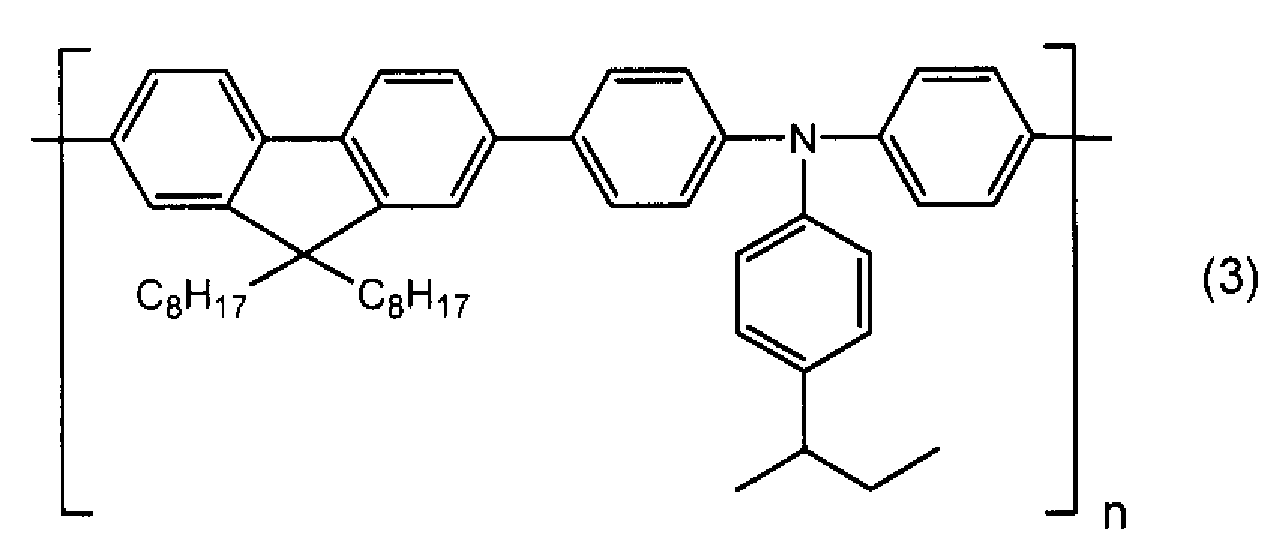
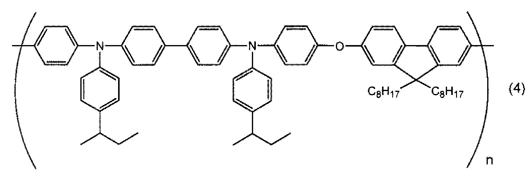
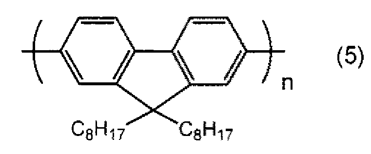
정공 수송성 화합물이 상기 화학식 (2)로 표시되는 화합물일 때, 상기 나노 입자의 보호제로서는, 하기 화학식 (6)으로 표시되는 화합물을 적절하게 사용할 수 있다.When the hole-transporting compound is a compound represented by the formula (2), a compound represented by the following formula (6) may be suitably used as a protective agent for the nanoparticle.
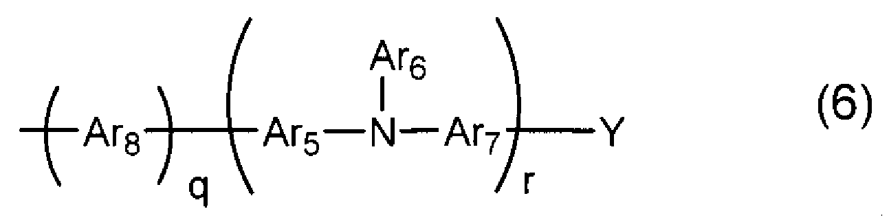
(단, 화학식 (6)에 있어서, Ar5 내지 Ar8은, 서로 동일해도 좋고 상이해도 좋고, 공액 결합에 관련되는 탄소 원자수가 6개 이상 60개 이하로 이루어지는 비치환 혹은 치환의 방향족 탄화수소기 또는 공액 결합에 관련되는 탄소 원자수가 4개 이상 60개 이하로 이루어지는 비치환 혹은 치환의 복소환기를 나타낸다. q는 0 내지 10, r는 0 내지 10이며, q+r=1 내지 20이다. 또한, 2개의 반복 단위의 배열은 임의이다. Y는 연결기를 나타낸다)(6), Ar 5 to Ar 8 may be the same or different and each represents an unsubstituted or substituted aromatic hydrocarbon group having 6 or more and 60 or less carbon atoms related to the conjugated bond or Q represents 0 to 10, r represents 0 to 10, and q + r = 1 to 20. In addition, the number of carbon atoms in the conjugated bond is not particularly limited, The arrangement of the two repeating units is arbitrary and Y represents a linking group)
상기 화학식 (6)의 Ar5 내지 Ar8에 있어서, 방향족 탄화수소기에 있어서의 방향족 탄화수소로서는, 구체적으로는 예를 들어, 벤젠, 플루오렌, 나프탈렌 및 안트라센 및 이들의 조합 및 그들의 유도체, 또한, 페닐렌비닐렌 유도체, 스티릴 유도체 등을 들 수 있다. 또한, 복소환기에 있어서의 복소환으로서는, 구체적으로는 예를 들어 티오펜, 피리딘, 피롤 및 카르바졸 및 이들의 조합 및 그들의 유도체 등을 들 수 있다. Ar5 내지 Ar8에 있어서도, 상기 화학식 (2)의 Ar1 내지 Ar4가 치환기를 갖는 경우와 마찬가지의 치환기를 갖고 있어도 좋다.Specific examples of aromatic hydrocarbons in the aromatic hydrocarbon group represented by Ar 5 to Ar 8 in the above formula (6) include benzene, fluorene, naphthalene, and anthracene, and combinations and derivatives thereof, and phenylene Vinylene derivatives, styryl derivatives, and the like. Specific examples of the heterocycle in the heterocyclic group include thiophene, pyridine, pyrrole and carbazole, and combinations and derivatives thereof. Also in Ar 5 to Ar 8 , Ar 1 to Ar 4 in the above formula (2) may have the same substituents as those in the case of having a substituent.
화학식 (6)에 있어서, Ar5, Ar6 및 Ar7의 조합 및/또는 Ar8은, 화학식 (2)에 있어서의 Ar1, Ar2 및 Ar3의 조합 및/또는 Ar1, Ar2, Ar3 및 Ar4 중 어느 하나와, 적어도 방향족 탄화수소기 또는 복소환기의 골격이 동일한 것이 바람직하다.In the formula (6), the combination of Ar 5 , Ar 6 and Ar 7 and / or Ar 8 is a combination of Ar 1 , Ar 2 and Ar 3 in the formula (2) and / or a combination of Ar 1 , Ar 2 , It is preferable that the skeleton of any one of Ar 3 and Ar 4 and at least the aromatic hydrocarbon group or heterocyclic group is the same.
본 발명의 정공 주입 수송층용 잉크에 있어서, 상기 정공 수송성 화합물이 사용되는 경우에는, 정공 수송성 화합물의 함유량은, 상기 전이 금속 함유 나노 입자 100질량부에 대하여, 10 내지 10000질량부인 것이, 정공 주입 수송성을 높게 하고, 또한, 막의 안정성이 높아 장수명을 달성하는 점에서 바람직하다.When the hole-transporting compound is used in the ink for a hole-injecting and transporting layer of the present invention, the content of the hole-transporting compound is preferably from 10 to 10,000 parts by mass based on 100 parts by mass of the transition metal-containing nanoparticles, And also the stability of the film is high and long life is attained.
정공 주입 수송층에 있어서, 상기 정공 수송성 화합물의 함유량이 지나치게 적으면, 정공 수송성 화합물을 혼합한 상승 효과가 얻어지기 어렵다. 한편, 상기 정공 수송성 화합물의 함유량이 지나치게 많으면, 전이 금속 함유 나노 입자를 사용하는 효과가 얻어지기 어려워진다.If the content of the hole-transporting compound is too small in the hole-injecting and transporting layer, it is difficult to obtain a synergistic effect of mixing the hole-transporting compound. On the other hand, if the content of the hole-transporting compound is excessively large, it becomes difficult to obtain the effect of using the transition metal-containing nanoparticles.
본 발명의 정공 주입 수송층용 잉크는, 본 발명의 효과를 손상시키지 않는 한, 바인더 수지나 경화성 수지나 도포성 개량제 등의 첨가제를 포함하고 있어도 좋다.The ink for a hole injection transport layer of the present invention may contain additives such as a binder resin, a curable resin, and a coating improver unless the effect of the present invention is impaired.
바인더 수지로서는, 폴리카르보네이트, 폴리스티렌, 폴리아릴레이트 및 폴리에스테르 등을 들 수 있다. 또한, 열 또는 광 등에 의해 경화되는 바인더 수지를 함유하고 있어도 좋다. 열 또는 광 등에 의해 경화되는 재료로서는, 상기 정공 수송성 화합물에 있어서 분자 내에 경화성의 관능기가 도입된 것, 혹은, 경화성 수지 등을 사용할 수 있다. 구체적으로, 경화성의 관능기로서는, 아크릴로일기나 메타크릴로일기 등의 아크릴계의 관능기, 비닐렌기, 에폭시기 및 이소시아네이트기 등을 들 수 있다.Examples of the binder resin include polycarbonate, polystyrene, polyarylate and polyester. Further, it may contain a binder resin which is cured by heat or light. As the material to be cured by heat or light, it is possible to use a material in which a curable functional group is introduced into the molecule or a curable resin in the hole-transporting compound. Specific examples of the curable functional group include acrylic functional groups such as acryloyl group and methacryloyl group, vinylene group, epoxy group and isocyanate group.
경화성 수지로서는, 열경화성 수지이어도 좋고 광경화성 수지이어도 좋은데, 예를 들어 에폭시 수지, 페놀 수지, 멜라민 수지, 폴리에스테르 수지, 폴리우레탄 수지, 실리콘 수지 및 실란 커플링제 등을 들 수 있다.The curable resin may be a thermosetting resin or a photo-curable resin, and examples thereof include an epoxy resin, a phenol resin, a melamine resin, a polyester resin, a polyurethane resin, a silicone resin and a silane coupling agent.
정공 주입 수송층용 잉크는, 통상 유기 용제에, 제1 정공 주입 수송층용 잉크에 있어서는 나노 입자, 제2 정공 주입 수송층용 잉크에 있어서는 전이 금속 탄화물, 전이 금속 질화물 및 전이 금속 황화물로 이루어지는 군에서 선택되는 1종 이상의 화합물 (C), 연결기 및 소수성의 유기기를 갖는 보호제라는 필수 성분 외에, 정공 수송성 화합물 등의 임의 성분을 일반적인 제조법에 따라, 혼합하여 분산 처리함으로써 제조된다. 혼합 분산에는, 페인트 셰이커 또는 비즈 밀 등을 사용할 수 있다.The ink for the hole injection and transport layer is usually selected from the group consisting of organic solvents, nanoparticles for the first hole injection transport layer ink, transition metal carbides for the second hole injection transport layer ink, transition metal nitrides and transition metal sulfides (C), an optional component such as a protective agent having a linking group and a hydrophobic organic group, and a hole-transporting compound, in accordance with a common preparation method, followed by dispersion treatment. For the mixed dispersion, a paint shaker or a bead mill can be used.
(디바이스) (device)
본 발명에 따른 디바이스는, 기판 상에 대향하는 2개 이상의 전극과, 그 중 2개의 전극 사이에 배치된 정공 주입 수송층을 갖는 디바이스이며, A device according to the present invention is a device having two or more opposite electrodes on a substrate and a hole injection and transport layer disposed between two of the electrodes,
상기 정공 주입 수송층이, 적어도 상기 전이 금속 화합물 함유 나노 입자를 함유하는 것을 특징으로 한다.And the hole injection transport layer contains at least the transition metal compound-containing nanoparticles.
본 발명의 디바이스는, 상기 정공 주입 수송층이, 나노 입자를 함유함으로써, 정공 주입 특성이 향상하고, 또한, 인접하는 전극이나 유기층과의 밀착성도 우수한, 안정성이 높은 막이 되기 때문에, 소자의 장수명화가 달성 가능하다. 또한, 본 발명의 디바이스는, 무기 화합물의 전이 금속 산화물을 사용하는 경우와 달리, 나노 입자에 있어서 입자 표면을 보호하는 보호제로서 유기기를 포함하고, 용제에 분산성을 갖기 때문에, 용액 도포법에 의해 박막 형성이 가능한 점에서, 제조 프로세스가 용이하다.In the device of the present invention, since the hole injection transport layer contains nanoparticles, the hole injection property is improved, and the film has high stability, which also has excellent adhesion with adjacent electrodes and organic layers. Therefore, It is possible. Further, unlike the case where the transition metal oxide of an inorganic compound is used, since the device of the present invention contains an organic group as a protecting agent for protecting the particle surface in nanoparticles and has a dispersibility in a solvent, Since the thin film can be formed, the manufacturing process is easy.
이와 같이, 본 발명의 디바이스에 사용되는 나노 입자가 수명을 향상시킬 수 있는 것은, 나노 입자에 포함되는 전이 금속 탄화 산화물, 전이 금속 질화 산화물 및 전이 금속 황화 산화물 등의 전이 금속 화합물의 반응성이 높아, 나노 입자끼리, 또는 정공 수송성 화합물이 포함되는 경우에는 당해 정공 수송성 화합물 사이에서, 전하 이동 착체를 형성하기 쉽기 때문으로 추측된다.As described above, the reason why the nanoparticles used in the device of the present invention can improve the lifetime is that the reactivity of the transition metal compound such as transition metal carbide oxides, transition metal nitride oxides, and transition metal sulfide oxides contained in the nanoparticles is high, It is presumed that when the nanoparticles or the hole-transporting compound are contained, the charge-transfer complex easily forms between the hole-transporting compound.
나노 입자는, 무기 화합물의 전이 금속 산화물과 달리, 나노 입자 중에 보호제로서 유기기를 포함하기 때문에, 유기물인 정공 수송성 화합물과의 상용성이 양호해지고, 또한, 인접하는 유기층과의 계면의 밀착성도 양호해진다. 그로 인해, 나노 입자를 함유하는 정공 주입 수송층을 구비한 본 발명의 디바이스는, 저 전압 구동, 고 전력 효율로, 특히 수명이 향상한 디바이스를 실현할 수 있다고 추측된다.Unlike the transition metal oxide of the inorganic compound, since the nanoparticles contain an organic group as a protective agent in the nanoparticles, the nanoparticles have good compatibility with the hole transporting compound as the organic material, and the adhesiveness of the interface with the adjacent organic layer is also good . Therefore, it is assumed that the device of the present invention including the hole injection and transport layer containing nanoparticles can realize a device with low voltage driving, high power efficiency, and particularly improved lifetime.
본 발명의 디바이스에 있어서는, 나노 입자의 보호제의 종류를 선택함으로써, 친수성·소수성, 전하 수송성, 혹은 밀착성 등의 기능성을 부여하는 등, 다기능화하는 것이 용이하다.In the device of the present invention, by selecting the kind of the nanoparticle protecting agent, functionalization such as hydrophilicity, hydrophobicity, charge transportability, or adhesion can be imparted, and it is easy to make it multifunctional.
본 발명의 디바이스는, 용액 도포법에 의해 정공 주입 수송층을 형성할 수 있으므로, 발액성 뱅크를 갖는 기판에 정공 주입 수송층부터 발광층까지를 순차 도포 프로세스만으로 형성할 수 있다. 그로 인해, 무기 화합물의 전이 금속 산화물의 경우와 같이 정공 주입층을 고정밀의 마스크 증착 등으로 증착한 후에, 정공 수송층이나 발광층을 용액 도포법으로 형성하고, 제2 전극을 더 증착하는 프로세스와 비교하여, 단순하게, 저비용으로 디바이스를 제작할 수 있는 이점이 있다.Since the device of the present invention can form the hole injecting and transporting layer by the solution coating method, the steps from the hole injecting and transporting layer to the light emitting layer can be formed on the substrate having the liquid repellent bank only by the sequential coating process. Therefore, as in the case of the transition metal oxide of the inorganic compound, the hole injection layer is deposited by high precision mask deposition or the like, and then the hole transport layer or the light emitting layer is formed by the solution coating method and the second electrode is further deposited , There is an advantage that a device can be manufactured simply and at low cost.
또한, 전하 이동 착체를 형성하고 있는 것은, 예를 들어 1H NMR 측정에 의해, 나노 입자를 전하 수송성 화합물의 용액에 혼합한 경우, 전하 수송성 화합물의 6 내지 10ppm 부근에서 관측되는 방향환에서 유래하는 프로톤 시그널의 형상이나 케미컬 시프트값이, 나노 입자를 혼합하기 전과 비교하여 변화하는 현상이 관측됨으로써 시사된다.The reason why the charge transfer complex is formed is that when the nanoparticles are mixed with the solution of the charge transporting compound by, for example, 1 H NMR measurement, the charge transporting compound is a compound derived from an aromatic ring observed at about 6 to 10 ppm of the charge transporting compound It is suggested that the phenomenon that the shape of the proton signal or the chemical shift value changes in comparison with that before mixing the nanoparticles is observed.
이하, 본 발명에 따른 디바이스의 층 구성에 대하여 설명한다.Hereinafter, the layer structure of the device according to the present invention will be described.
본 발명에 따른 디바이스는, 기판 상에 대향하는 2개 이상의 전극과, 그 중 2개의 전극 사이에 배치된 정공 주입 수송층을 갖는 디바이스이다.A device according to the present invention is a device having two or more electrodes opposed to each other on a substrate and a hole injection and transport layer disposed between two of the electrodes.
본 발명에 따른 디바이스에는, 유기 EL 소자, 유기 트랜지스터, 색소 증감 태양 전지, 유기 박막 태양 전지, 유기 반도체를 포함하는 유기 디바이스 외에, 정공 주입 수송층을 갖는 양자 도트 발광 소자, 산화물계 화합물 태양 전지 등도 포함된다.The device according to the present invention may include an organic EL device, an organic transistor, a dye-sensitized solar cell, an organic thin film solar cell, an organic device including an organic semiconductor, a quantum dot light emitting device having a hole injecting and transporting layer, do.
도 2는 본 발명에 따른 유기 디바이스의 기본적인 층 구성을 도시하는 단면 모식도이다. 본 발명의 디바이스의 기본적인 층 구성은, 기판(50) 상에 대향하는 2개의 전극(61 및 62)과, 그 2개의 전극(61 및 62) 사이에 배치되고 적어도 정공 주입 수송층(70)을 포함하는 유기층(80)을 갖는다.2 is a schematic cross-sectional view showing a basic layer structure of an organic device according to the present invention. The basic layer structure of the device of the present invention is composed of two
기판(50)은, 디바이스를 구성하는 각 층을 형성하기 위한 지지체이며, 반드시 전극(61)의 표면에 설치될 필요는 없으며, 디바이스의 가장 외측의 면에 설치되어 있으면 된다.The
정공 주입 수송층(70)은, 적어도 상기 나노 입자를 함유하고, 전극(61)으로부터 유기층(80)으로의 정공의 주입 및/또는 수송을 담당하는 층이다.The hole injection and
유기층(80)은, 정공 주입 수송됨으로써, 디바이스의 종류에 따라 여러 기능을 발휘하는 층이며, 단층으로 이루어지는 경우와 다층으로 이루어지는 경우가 있다. 유기층이 다층으로 이루어지는 경우에는, 유기층은, 정공 주입 수송층 외에 디바이스의 기능의 중심이 되는 층(이하, 기능층이라고 호칭한다)이나, 당해 기능층의 보조적인 층(이하, 보조층이라고 호칭한다)을 더 포함하고 있다. 예를 들어, 유기 EL 소자의 경우, 정공 주입 수송층의 표면에 더 적층되는 정공 수송층이 보조층에 해당하고, 당해 정공 수송층의 표면에 적층되는 발광층이 기능층에 해당한다.The
전극(62)은, 대향하는 전극(61)과의 사이에 정공 주입 수송층(70)을 포함하는 유기층(80)이 존재하는 장소에 형성된다. 또한, 필요에 따라, 도시하지 않은 제3 전극을 가져도 좋다. 이들 전극 사이에 전기장을 인가함으로써, 디바이스의 기능을 발현시킬 수 있다.The
도 3은, 본 발명에 따른 디바이스의 일 실시 형태인 유기 EL 소자의 층 구성의 일례를 도시하는 단면 모식도이다. 본 발명의 유기 EL 소자는, 전극(61)의 표면에 정공 주입 수송층(70)이 적층되고, 당해 정공 주입 수송층(70)의 표면에 보조층으로서 정공 수송층(90a), 기능층으로서 발광층(100)이 적층된 형태를 갖는다. 이와 같이, 본 발명에 특징적인 정공 주입 수송층을 정공 주입층의 위치에서 사용하는 경우에는, 도전율의 향상 외에, 당해 정공 주입 수송층은 전하 이동 착체를 형성하여 용액 도포법에 사용한 용제에 불용이 되므로, 상층의 정공 수송층을 적층할 때에도 용액 도포법을 적용하는 것이 가능하다. 또한, 전극과의 밀착성 향상도 기대할 수 있다.Fig. 3 is a schematic cross-sectional view showing an example of the layer structure of the organic EL element which is one embodiment of the device according to the present invention. The organic EL device of the present invention is characterized in that a hole injection and
도 4는, 본 발명에 따른 디바이스의 일 실시 형태인 유기 EL 소자의 층 구성의 다른 일례를 도시하는 단면 모식도이다. 본 발명의 유기 EL 소자는, 전극(61)의 표면에 보조층으로서 정공 주입층(90b)이 형성되고, 당해 정공 주입층(90b)의 표면에 정공 주입 수송층(70), 기능층으로서 발광층(100)이 적층된 형태를 갖는다. 이와 같이, 본 발명에 특징적인 정공 주입 수송층을 정공 수송층의 위치에서 사용하는 경우에는, 도전율의 향상 외에, 당해 정공 주입 수송층은 전하 이동 착체를 형성하여 용액 도포법에 사용한 용제에 불용이 되므로, 상층의 발광층을 적층할 때에도 용액 도포법을 적용하는 것이 가능하다.4 is a cross-sectional schematic diagram showing another example of the layer structure of the organic EL element which is one embodiment of the device according to the present invention. In the organic EL device of the present invention, a
도 5는, 본 발명에 따른 디바이스의 일 실시 형태인 유기 EL 소자의 층 구성의 다른 일례를 도시하는 단면 모식도이다. 본 발명의 유기 EL 소자는, 전극(61)의 표면에 정공 주입 수송층(70), 기능층으로서 발광층(100)이 순차 적층된 형태를 갖는다. 이와 같이, 본 발명에 특징적인 정공 주입 수송층을 1층으로 사용하는 경우에는, 공정 수가 삭감된다는 프로세스 상의 장점이 있다.5 is a schematic cross-sectional view showing another example of the layer structure of the organic EL element which is one embodiment of the device according to the present invention. The organic EL device of the present invention has a form in which a hole injecting and transporting
또한, 상기 도 3 내지 도 5에 있어서는, 정공 주입 수송층(70), 정공 수송층(90a), 정공 주입층(90b) 각각이, 단층이 아니고 복수층으로 구성되어 있는 것이어도 좋다.3 to 5, each of the hole injecting and transporting
상기 도 3 내지 도 5에 있어서는, 전극(61)은 양극, 전극(62)은 음극으로서 기능한다. 상기 유기 EL 소자는, 양극과 음극 사이에 전기장을 인가하면, 정공이 양극으로부터 정공 주입 수송층(70) 및 정공 수송층(90a)을 거쳐 발광층(100)에 주입되고, 또한, 전자가 음극으로부터 발광층에 주입됨으로써, 발광층(100)의 내부에서 주입된 정공과 전자가 재결합하여, 소자의 외부에 발광하는 기능을 갖는다.3 to 5, the
소자의 외부에 광을 방사하기 위해, 발광층 중 적어도 한쪽의 면에 존재하는 모든 층은, 가시 파장 영역 중 적어도 일부 파장의 광에 대한 투과성을 갖는 것을 필요로 한다. 또한, 도시하지 않았지만, 발광층과 전극(62)(음극) 사이에는, 필요에 따라 전자 수송층 및/또는 전자 주입층이 형성되어 있어도 좋다.In order to emit light to the outside of the device, all layers present on at least one surface of the light emitting layer need to have transparency to light of at least a part of the wavelength of visible light. Although not shown, an electron transporting layer and / or an electron injecting layer may be formed between the light emitting layer and the electrode 62 (cathode) as necessary.
도 6은, 본 발명에 따른 디바이스의 다른 실시 형태인 유기 트랜지스터의 층 구성의 일례를 도시하는 단면 모식도이다. 이 유기 트랜지스터는, 기판(50) 상에 전극(63)(게이트 전극)과, 대향하는 전극(61)(소스 전극) 및 전극(62)(드레인 전극)과, 전극(63), 전극(61) 및 전극(62) 사이에 배치된 상기 유기층으로서의 유기 반도체층(110)과, 전극(63)과 전극(61) 사이 및 전극(63)과 전극(61) 사이에 개재하는 절연층(120)을 갖고, 전극(61)과 전극(62)의 표면에, 정공 주입 수송층(70)이 형성되어 있다.6 is a schematic cross-sectional view showing an example of the layer structure of an organic transistor which is another embodiment of the device according to the present invention. This organic transistor includes an electrode 63 (gate electrode), an opposing electrode 61 (source electrode) and an electrode 62 (drain electrode), an
상기 유기 트랜지스터는, 게이트 전극에 있어서의 전하의 축적을 제어함으로써, 소스 전극-드레인 전극 사이의 전류를 제어하는 기능을 갖는다.The organic transistor has a function of controlling the current between the source electrode and the drain electrode by controlling the accumulation of charges in the gate electrode.
도 7은, 본 발명에 따른 디바이스의 실시 형태인 유기 트랜지스터의 다른 층 구성의 일례를 도시하는 단면 모식도이다. 이 유기 트랜지스터는, 기판(50) 상에 전극(63)(게이트 전극)과, 대향하는 전극(61)(소스 전극) 및 전극(62)(드레인 전극)과, 전극(63), 전극(61) 및 전극(62) 사이에 배치된 상기 유기층으로서 본 발명의 정공 주입 수송층(70)을 형성하여 유기 반도체층(110)으로 하고 전극(63)과 전극(61) 사이 및 전극(63)과 전극(62) 사이에 개재하는 절연층(120)을 갖고 있다. 이 예에 있어서는, 정공 주입 수송층(70)이 유기 반도체층(110)으로 되어 있다.7 is a schematic cross-sectional view showing an example of another layer structure of an organic transistor which is an embodiment of the device according to the present invention. This organic transistor includes an electrode 63 (gate electrode), an opposing electrode 61 (source electrode) and an electrode 62 (drain electrode), an
또한, 본 발명의 디바이스의 층 구성은, 상기 예시에 한정되는 것이 아니라, 본 발명의 특허청구범위에 기재된 기술적 사상과 실질적으로 동일한 구성을 갖고, 마찬가지의 작용 효과를 발휘하는 것은, 어떠한 것이든 본 발명의 기술적 범위에 포함된다.The layer structure of the device of the present invention is not limited to the above-described example. The layer structure of the device of the present invention is substantially the same as the technical idea described in the claims of the present invention, And are included in the technical scope of the invention.
이하, 본 발명에 따른 디바이스의 각 층에 대하여 상세하게 설명한다.Hereinafter, each layer of the device according to the present invention will be described in detail.
(정공 주입 수송층) (Hole injection and transport layer)
본 발명의 디바이스는, 적어도 정공 주입 수송층을 포함한다. 본 발명의 디바이스가 유기 디바이스이며, 유기층이 다층인 경우에는, 유기층은, 정공 주입 수송층 이외에, 디바이스의 기능의 중심이 되는 층이나, 당해 기능층을 보조하는 역할을 담당하는 보조층을 더 포함하고 있지만, 이들 기능층이나 보조층은, 후술하는 디바이스의 구체예에서 상세하게 설명한다.The device of the present invention includes at least a hole injection transport layer. In the case where the device of the present invention is an organic device and the organic layer is a multilayer, the organic layer may further include a layer serving as a center of the function of the device or an auxiliary layer serving to assist the functional layer in addition to the hole injection transport layer However, these functional layers and auxiliary layers will be described in detail in specific examples of devices to be described later.
본 발명의 디바이스에 있어서의 정공 주입 수송층은, 상기 정공 주입 수송층용 잉크를 사용하여 형성되고, 적어도 나노 입자를 함유하는 것이다. 본 발명의 디바이스에 있어서의 정공 주입 수송층은, 나노 입자로만 이루어지는 것이어도 좋지만, 다른 성분을 더 함유하고 있어도 좋다. 그 중에서도, 정공 수송성 화합물을 함유하는 것이, 구동 전압의 저하나 소자 수명을 더 향상시키는 점에서, 바람직하다.The hole injection transport layer in the device of the present invention is formed using the ink for the hole injection transport layer and contains at least nanoparticles. The hole injection transport layer in the device of the present invention may be composed of only nanoparticles, but may further contain other components. Among them, it is preferable to contain a hole-transporting compound in view of further lowering the driving voltage and further improving the lifetime of the device.
정공 수송성 화합물을 함유하는 경우에, 본 발명의 디바이스에 있어서의 정공 주입 수송층은, 나노 입자와 정공 수송성 화합물을 함유하는 혼합층 1층으로 이루어지는 것이어도 좋고, 당해 혼합층을 포함하는 복수층으로 이루어지는 것이어도 좋다. 또한, 상기 정공 주입 수송층은, 나노 입자를 함유하는 층과, 정공 수송성 화합물을 함유하는 층이 적어도 적층된 복수층으로 이루어지는 것이어도 좋다. 또한, 상기 정공 주입 수송층은, 나노 입자를 함유하는 층과, 나노 입자 및 정공 수송성 화합물을 적어도 함유하는 층이 적어도 적층된 층으로 이루어지는 것이어도 좋다.In the case of containing the hole-transporting compound, the hole-injecting and transporting layer in the device of the present invention may be composed of one mixed layer containing nanoparticles and a hole-transporting compound, and may be composed of a plurality of layers including the mixed layer good. The hole injecting and transporting layer may be composed of a plurality of layers including at least a layer containing nanoparticles and a layer containing a hole transporting compound. The hole injecting and transporting layer may be composed of a layer including at least a layer containing nanoparticles and a layer containing at least nanoparticles and a hole transporting compound.
본 발명의 정공 주입 수송층은, 포함되는 전이 금속이 각각 상이한 2종 이상의 전이 금속 화합물 함유 나노 입자를 함유하고 있어도 좋다.The hole injecting and transporting layer of the present invention may contain two or more transition metal compound-containing nanoparticles each containing a different transition metal.
상기 정공 주입 수송층의 막 두께는, 목적이나 인접하는 층에 따라 적절히 결정할 수 있지만, 통상 0.1 내지 1000nm, 바람직하게는 1 내지 500nm이다.The film thickness of the hole injection transporting layer can be appropriately determined depending on the purpose or the adjacent layer, but is usually from 0.1 to 1000 nm, preferably from 1 to 500 nm.
또한, 상기 정공 주입 수송층의 일함수는 5.0 내지 6.0eV가 바람직하고, 5.0 내지 5.8eV인 것이, 정공 주입 효율의 관점에서 보다 바람직하다.The work function of the hole injection transport layer is preferably 5.0 to 6.0 eV, more preferably 5.0 to 5.8 eV in view of hole injection efficiency.
본 발명의 정공 주입 수송층은, 용액 도포법으로 형성하는 것이 가능하다. 본 발명의 정공 주입 수송층은, 용액 도포법에 의해 형성되는 것이, 제조 프로세스가 용이한 데다가, 쇼트가 발생하기 어렵기 때문에 수율이 높고, 전하 이동 착체를 형성하여 장수명을 달성하는 점에서 바람직하다. 이 경우, 본 발명의 정공 주입 수송층은, 적어도 나노 입자가 양호하게 분산하는 용제 중에서 분산시킨 용액(정공 주입 수송층용 잉크)을 사용하여, 용액 도포법에 의해 형성한다. 또한, 정공 수송성 화합물이 포함되는 정공 주입 수송층을 형성하는 경우, 나노 입자와, 정공 수송성 화합물을, 양쪽이 양호하게 용해 내지 분산하는 용제 중에서 혼합한 용액을 사용하여, 용액 도포법에 의해 형성해도 좋다. 이 경우, 나노 입자와 정공 수송성 화합물의 양쪽이 양호하게 용해 내지 분산하는 용제 중에서 혼합하면, 용액 중에서 나노 입자와 정공 수송성 화합물이 상호 작용하여, 전하 이동 착체를 형성하기 쉬워지기 때문에, 정공 수송성 및 막의 경시 안정성이 우수한 정공 주입 수송층을 형성할 수 있다. 이렇게 전하 이동 착체를 형성한 정공 주입 수송층은, 정공 주입 수송층을 형성할 때에 사용한 용제에 불용이 되는 경향이 있어, 당해 정공 주입 수송층의 상층에 해당하는 유기층을 형성하는 경우도, 당해 정공 주입 수송층을 용출시키지 않고 용액 도포법을 사용할 가능성이 넓어진다.The hole injecting and transporting layer of the present invention can be formed by a solution coating method. The hole injecting and transporting layer of the present invention is preferably formed by a solution coating method because it is easy to manufacture and is less prone to short-circuiting, is highly yieldable, forms a charge transfer complex and achieves long life. In this case, the hole injecting and transporting layer of the present invention is formed by a solution coating method using a solution (an ink for a hole injecting and transporting layer) dispersed in a solvent in which at least nanoparticles are well dispersed. When the hole injecting and transporting layer containing the hole transporting compound is formed, the nanoparticles and the hole transporting compound may be formed by a solution coating method using a solution in which both of them are dissolved or dispersed well . In this case, when both the nanoparticles and the hole-transporting compound are mixed in a solvent which is dissolved or dispersed well, the nanoparticles and the hole-transporting compound interact with each other in the solution to easily form a charge transfer complex, A hole injecting and transporting layer having excellent stability over time can be formed. The hole injecting and transporting layer having the charge transfer complex formed thereon tends to be insoluble in the solvent used for forming the hole injecting and transporting layer. Even when the organic layer corresponding to the upper layer of the hole injecting and transporting layer is formed, The possibility of using a solution coating method without elution is widened.
용액 도포법에 대해서는, 하기 디바이스의 제조 방법의 항목에서 설명한다.The solution coating method is described in the item of the manufacturing method of the following device.
(기판) (Board)
기판은, 본 발명의 디바이스의 지지체로 되는 것이며, 예를 들어 유연한 재질이어도 좋고, 경질의 재질이어도 좋다. 구체적으로 사용할 수 있는 재료로서는, 예를 들어 유리, 석영, 폴리에틸렌, 폴리프로필렌, 폴리에틸렌테레프탈레이트, 폴리메타크릴레이트, 폴리메틸메타크릴레이트, 폴리메틸아크릴레이트, 폴리에스테르 및 폴리카르보네이트 등을 들 수 있다.The substrate is a support for the device of the present invention, and may be, for example, a flexible material or a hard material. Specific examples of the material that can be used include glass, quartz, polyethylene, polypropylene, polyethylene terephthalate, polymethacrylate, polymethyl methacrylate, polymethylacrylate, polyester and polycarbonate. .
이들 중, 합성 수지제의 기판을 사용하는 경우에는, 가스 배리어성을 갖는 것이 바람직하다. 기판의 두께는 특별히 한정되지 않지만, 통상 0.5 내지 2.0mm 정도이다.Of these, in the case of using a substrate made of a synthetic resin, it is preferable to have a gas barrier property. The thickness of the substrate is not particularly limited, but is usually about 0.5 to 2.0 mm.
(전극) (electrode)
본 발명의 디바이스는, 기판 상에 대향하는 2개 이상의 전극을 갖는다.The device of the present invention has two or more electrodes facing on a substrate.
본 발명의 디바이스에 있어서, 전극은, 금속 또는 금속 산화물로 형성되는 것이 바람직하고, 공지의 재료를 적절히 채용할 수 있다. 통상, 알루미늄, 금, 은, 니켈, 팔라듐 및 백금 등의 금속 및 인듐 및/또는 주석의 산화물 등의 금속 산화물에 의해 형성할 수 있다.In the device of the present invention, the electrode is preferably formed of a metal or a metal oxide, and a known material can be suitably employed. It is usually formed of a metal such as aluminum, gold, silver, nickel, palladium and platinum, and a metal oxide such as indium and / or tin oxide.
전극은, 통상 기판 상에 스퍼터링법, 진공 증착법 등의 방법에 의해 형성되는 경우가 많지만, 도포법이나 침지법 등의 습식법에 의해 형성할 수도 있다. 전극의 두께는, 각각의 전극에 요구되는 투명성 등에 따라 상이하다. 투명성이 필요한 경우에는, 전극의 가시광 파장 영역의 광투과율이, 통상 60% 이상, 바람직하게는 80% 이상이 되는 것이 바람직하고, 이 경우의 두께는, 통상 10 내지 1000nm, 바람직하게는 20 내지 500nm 정도이다.The electrode is usually formed on a substrate by a sputtering method, a vacuum evaporation method, or the like, but may be formed by a wet method such as a coating method or a dipping method. The thickness of the electrode differs depending on the transparency required for each electrode and the like. When transparency is required, it is preferable that the light transmittance in the visible light wavelength region of the electrode is generally 60% or more, preferably 80% or more, and the thickness in this case is usually 10 to 1000 nm, preferably 20 to 500 nm Respectively.
본 발명에 있어서는, 전극 상에, 전하 주입 재료와의 밀착 안정성을 향상시키기 위해, 금속층을 더 갖고 있어도 좋다. 금속층은 금속이 포함되는 층을 의미하고, 상술한 바와 같은 통상 전극에 사용되는 금속이나 금속 산화물로 형성된다.In the present invention, a metal layer may be further provided on the electrode in order to improve the adhesion stability with the charge injecting material. The metal layer means a layer containing a metal and is formed of a metal or a metal oxide used for a conventional electrode as described above.
(기타) (Etc)
본 발명의 디바이스는, 필요에 따라, 전자 주입 전극과 유기층 사이에, 종래 공지의 전자 주입층 및/또는 전자 수송층을 가져도 좋다.The device of the present invention may have a conventionally known electron injection layer and / or electron transport layer between the electron injection electrode and the organic layer, if necessary.
(유기 EL 소자) (Organic EL device)
본 발명의 디바이스의 일 실시 형태로서, 적어도 본 발명의 정공 주입 수송층 및 발광층을 포함하는 유기층을 함유하는, 유기 EL 소자를 들 수 있다.As an embodiment of the device of the present invention, there is an organic EL element containing at least an organic layer including a hole injection transport layer and a light emitting layer of the present invention.
이하, 유기 EL 소자를 구성하는 각 층에 대해서, 도 3 내지 도 5를 사용하여 순서대로 설명한다.Hereinafter, each layer constituting the organic EL element will be described in order with reference to Figs. 3 to 5. Fig.
(기판) (Board)
기판(50)은, 유기 EL 소자의 지지체로 되는 것이며, 예를 들어 유연한 재질이어도 좋고, 경질의 재질이어도 좋다. 구체적으로는, 예를 들어 상기 디바이스의 기판의 설명에서 예시한 것을 사용할 수 있다.The
발광층(100)에서 발광한 광이 기판(50)측을 투과하여 취출되는 경우에 있어서는, 적어도 그 기판(50)이 투명한 재질일 필요가 있다.When the light emitted from the
(양극, 음극) (Anode, cathode)
전극(61) 및 전극(62)은, 발광층(100)에서 발광한 광의 취출 방향에 따라, 어느 쪽의 전극에 투명성이 요구되는지의 여부가 상이한데, 기판(50)측으로부터 광을 취출하는 경우에는 전극(61)을 투명한 재료로 형성할 필요가 있고, 또한 전극(62)측으로부터 광을 취출하는 경우에는 전극(62)을 투명한 재료로 형성할 필요가 있다.The
기판(50)의 발광층측에 형성되어 있는 전극(61)은, 발광층에 정공을 주입하는 양극으로서 작용하고, 기판(50)의 발광층측에 형성되어 있는 전극(62)은, 발광층(100)에 전자를 주입하는 음극으로서 작용한다.The
본 발명에 있어서, 양극 및 음극은, 상기 디바이스의 전극의 설명에서 열거한 금속 또는 금속 산화물로 형성되는 것이 바람직하다.In the present invention, it is preferable that the anode and the cathode are formed of a metal or a metal oxide listed in the description of the electrode of the device.
(정공 주입 수송층, 정공 수송층 및 정공 주입층) (Hole injection transport layer, hole transport layer and hole injection layer)
정공 주입 수송층(70), 정공 수송층(90a) 및 정공 주입층(90b)은, 도 3 내지 도 5에 도시한 바와 같이, 발광층(100)과 전극(61)(양극) 사이에 적절히 형성된다. 도 3과 같이, 본 발명에 따른 정공 주입 수송층(70) 상에 정공 수송층(90a)을 적층하고, 그 위에 발광층(100)을 적층해도 좋고, 도 4와 같이, 정공 주입층(90b) 상에 본 발명에 따른 정공 주입 수송층(70)을 적층하고, 그 위에 발광층(100)을 적층해도 좋고, 도 5와 같이, 전극(61) 상에 본 발명에 따른 정공 주입 수송층(70)을 적층하고 그 위에 발광층(100)을 적층해도 좋다.The hole injection and
도 3과 같이, 본 발명에 따른 정공 주입 수송층(70) 상에 정공 수송층(90a)을 적층하는 경우에, 정공 수송층(90a)에 사용되는 정공 수송 재료는 특별히 한정되지 않는다. 본 발명에 따른 정공 주입 수송층에서 설명한 정공 수송성 화합물을 사용하는 것이 바람직하다. 그 중에서도, 인접하는 본 발명에 따른 정공 주입 수송층(70)에 사용되고 있는 정공 수송성 화합물과 동일한 화합물을 사용하는 것이, 정공 주입 수송층과 정공 수송층의 계면의 밀착 안정성을 향상시켜, 장기 구동 수명화에 기여하는 점에서 바람직하다.As shown in Fig. 3, when the
정공 수송층(90a)은, 정공 수송 재료를 사용하여, 후술하는 발광층과 마찬가지 방법으로 형성할 수 있다. 정공 수송층(90a)의 막 두께는, 통상 0.1 내지 1㎛, 바람직하게는 1 내지 500nm이다.The
도 4와 같이, 정공 주입층(90b) 상에 본 발명에 따른 정공 주입 수송층(70)을 적층하는 경우에, 정공 주입층(90b)에 사용되는 정공 주입 재료는 특별히 한정되지 않고 종래 공지의 화합물을 사용할 수 있다. 예를 들어, 페닐아민계, 스타버스트형 아민계, 프탈로시아닌계, 산화바나듐, 산화몰리브덴, 산화루테늄, 산화알루미늄 등의 산화물, 아몰퍼스 카본, 폴리아닐린, 폴리티오펜 유도체 등을 들 수 있다.4, in the case of laminating the hole injecting and transporting
정공 주입층(90b)은, 정공 주입 재료를 사용하여, 후술하는 발광층(100)과 마찬가지 방법으로 형성할 수 있다. 정공 주입층(90b)의 막 두께는, 통상 1nm 내지 1㎛, 바람직하게는 2nm 내지 500nm, 더욱 바람직하게는 5nm 내지 200nm이다.The
또한, 정공 주입 특성을 고려하면, 전극(61)측으로부터 유기층인 발광층(100)을 향하여 각 층의 일함수(HOMO)의 값이 계단 형상으로 커지는 정공 주입 재료 및 정공 수송 재료를 선택하고, 각 계면에서의 정공 주입의 에너지 장벽을 가능한 한 작게 하여, 전극(61)과 발광층(100) 사이의 큰 정공 주입의 에너지 장벽을 보완하는 것이 바람직하다.Considering the hole injecting property, a hole injecting material and a hole transporting material in which the value of the work function (HOMO) of each layer increases stepwise from the
구체적으로는 예를 들어, 전극(61)에 ITO(UV 오존 세정 직후의 일함수 5.0eV)를 사용하고, 발광층(100)에 Alq3(HOMO 5.7eV)를 사용한 경우, 정공 주입 수송층(70)을 구성하는 재료로서 TFB(일함수 5.4eV)와 나노 입자(일함수 5.0 내지 5.7eV)의 혼합물과 같은 것으로 선택하여, 전극(61)측으로부터 발광층(100)을 향하여 각 층의 일함수의 값이 순서대로 커지는 층 구성을 취하도록 배치하는 것이 바람직하다. 또한, 상기 일함수 또는 HOMO의 값은, 광전자 분광 장치 AC-1(리껭 게끼(주)제)을 사용한 광전자 분광법의 측정값으로부터 인용했다.Specifically, for example, when ITO (work function 5.0 eV immediately after UV ozone cleaning) is used for the
이러한 층 구성의 경우, 전극(61)(UV 오존 세정 직후의 일함수 5.0eV)과 발광층(100)(예를 들어 HOMO 5.7eV) 사이의 정공 주입이 큰 에너지 장벽을, HOMO의 값이 계단 형상으로 되도록 보완 가능하여, 정공 주입 효율이 매우 우수한 정공 주입 수송층이 얻어진다.In the case of such a layer structure, hole injection between the electrode 61 (work function 5.0 eV immediately after UV ozone cleaning) and the light emitting layer 100 (for example, HOMO 5.7 eV) has a large energy barrier, So that a hole injecting and transporting layer having an excellent hole injecting efficiency can be obtained.
(발광층) (Light emitting layer)
발광층(100)은, 도 3 내지 도 5에 도시한 바와 같이, 전극(61)이 형성된 기판(50)과 전극(62) 사이에, 발광 재료에 의해 형성된다.The
본 발명의 발광층에 사용되는 재료로서는, 통상 발광 재료로서 사용되고 있는 재료이면 특별히 한정되지 않고 형광 재료 및 인광 재료 모두 사용할 수 있다. 구체적으로는, 색소계 발광 재료, 금속 착체계 발광 재료 등의 재료를 들 수 있고, 저분자 화합물 또는 고분자 화합물 모두 사용할 수 있다.The material used for the light-emitting layer of the present invention is not particularly limited as long as it is a material usually used as a light-emitting material, and both a fluorescent material and a phosphorescent material can be used. Specifically, a material such as a dye-based light-emitting material or a metal complex-based light-emitting material can be used, and a low molecular weight compound or a high molecular weight compound can be used.
색소계 발광 재료로서는, 예를 들어 아릴아민 유도체, 안트라센 유도체, (페닐안트라센 유도체), 옥사디아졸 유도체, 옥사졸 유도체, 올리고티오펜 유도체, 카르바졸 유도체, 시클로펜타디엔 유도체, 실롤 유도체, 디스티릴벤젠 유도체, 디스티릴피라진 유도체, 디스티릴아릴렌 유도체, 실롤 유도체, 스틸벤 유도체, 스피로 화합물, 티오펜환 화합물, 테트라페닐부타디엔 유도체, 트리아졸 유도체, 트리페닐아민 유도체, 트리푸마닐아민 유도체, 피라졸로퀴놀린 유도체, 히드라존 유도체, 피라졸린 이량체, 피리딘환 화합물, 플루오렌 유도체, 페난트롤린류, 페리논 유도체, 페릴렌 유도체 등을 들 수 있다. 또한 이들의 이량체나 삼량체나 올리고머, 2종류 이상의 유도체의 화합물도 사용할 수 있다.Examples of the dye-based light-emitting material include, for example, arylamine derivatives, anthracene derivatives, (phenylanthracene derivatives), oxadiazole derivatives, oxazole derivatives, oligothiophene derivatives, carbazole derivatives, cyclopentadiene derivatives, Benzene derivatives, distyrylpyrazine derivatives, distyrylarylene derivatives, silole derivatives, stilbene derivatives, spiro compounds, thiophene ring compounds, tetraphenylbutadiene derivatives, triazole derivatives, triphenylamine derivatives, tripyranylamine derivatives, Quinoline derivatives, hydrazone derivatives, pyrazoline dimers, pyridine ring compounds, fluorene derivatives, phenanthrolines, perinone derivatives, and perylene derivatives. Further, these dimers, trimers, oligomers, and compounds of two or more derivatives can also be used.
이들 재료는 단독으로 사용해도 좋고 2종 이상을 병용해도 좋다.These materials may be used alone or in combination of two or more.
금속 착체계 발광 재료로서는, 예를 들어 알루미늄퀴놀리놀 착체, 벤조퀴놀리놀베릴륨 착체, 벤조옥사졸아연 착체, 벤조티아졸아연 착체, 아조메틸아연 착체, 포르피린아연 착체, 유로퓸 착체 등, 혹은 중심 금속으로 Al, Zn, Be 등 또는, Tb, Eu, Dy 등의 희토류 금속을 갖고, 배위자에 옥사디아졸, 티아디아졸, 페닐피리딘, 페닐벤즈이미다졸, 퀴놀린 구조 등을 갖는 금속 착체를 들 수 있다.Examples of the metal complex system light emitting material include metal complexes such as aluminum quinolinol complex, benzoquinolinol beryllium complex, benzooxazole zinc complex, benzothiazole zinc complex, azomethyl zinc complex, porphyrin zinc complex, europium complex, Metal complexes having a rare earth metal such as Al, Zn, Be or the like, or a rare earth metal such as Tb, Eu or Dy as the metal and oxadiazole, thiadiazole, phenylpyridine, phenylbenzimidazole or quinoline structure as the ligand have.
이들 재료는 단독으로 사용해도 좋고 2종 이상을 병용해도 좋다.These materials may be used alone or in combination of two or more.
고분자계 발광 재료로서는, 분자 내에 상기 저분자계 재료를 분자 내에 직쇄 혹은 측쇄 혹은 관능기로서 도입한, 중합체 및 덴드리머 등을 사용할 수 있다.As the polymer light emitting material, a polymer and a dendrimer in which the above low molecular weight material is introduced into the molecule as linear chains or side chains or functional groups in the molecule can be used.
예를 들어, 폴리파라페닐렌비닐렌 유도체, 폴리티오펜 유도체, 폴리파라페닐렌 유도체, 폴리실란 유도체, 폴리아세틸렌 유도체, 폴리비닐카르바졸, 폴리플루오레논 유도체, 폴리플루오렌 유도체 및 폴리퀴녹살린 유도체 및 그들의 공중합체 등을 들 수 있다.For example, there may be mentioned polyparaphenylenevinylene derivatives, polythiophene derivatives, polyparaphenylene derivatives, polysilane derivatives, polyacetylene derivatives, polyvinylcarbazole, polyfluorenone derivatives, polyfluorene derivatives and polyquinoxaline derivatives And copolymers thereof.
상기 발광층 중에는, 발광 효율의 향상이나 발광 파장을 변화시키는 등의 목적으로 도핑 재료를 첨가해도 좋다. 고분자계 재료의 경우에는, 이들을 분자 구조 중에 발광기로서 포함하고 있어도 좋다. 이러한 도핑 재료로서는, 예를 들어 페릴렌 유도체, 쿠마린 유도체, 루브렌 유도체, 퀴나크리돈 유도체, 스쿠아릴륨 유도체, 포르피린 유도체, 스티릴계 색소, 테트라센 유도체, 피라졸린 유도체, 데카시클렌, 페녹사존, 퀴녹살린 유도체, 카르바졸 유도체 및 플루오렌 유도체를 들 수 있다. 또한 이들에 스피로기를 도입한 화합물도 사용할 수 있다.A doping material may be added to the light emitting layer for the purpose of improving the light emitting efficiency or changing the light emitting wavelength. In the case of high molecular weight materials, they may be contained in the molecular structure as a light emitting device. Examples of such doping materials include perylene derivatives, coumarin derivatives, rubrene derivatives, quinacridone derivatives, squarylium derivatives, porphyrin derivatives, styryl type pigments, tetracene derivatives, pyrazoline derivatives, decacyclene, Quinoxaline derivatives, carbazole derivatives, and fluorene derivatives. Further, a compound in which a spiro group is introduced into these can also be used.
이들 재료는 단독으로 사용해도 좋고 2종 이상을 병용해도 좋다.These materials may be used alone or in combination of two or more.
본 발명에 있어서는, 발광층의 재료로서는 형광 발광하는 저분자 화합물 또는 고분자 화합물이나, 인광 발광하는 저분자 화합물 또는 고분자 화합물 어느 것이든 사용할 수 있다. 본 발명에 있어서, 발광층을 형성하는 베이스층이 본 발명의 상기 정공 주입 수송층인 경우, 당해 정공 주입 수송층은 전하 이동 착체를 형성하여 용액 도포법에 사용한 크실렌 등의 비수계 용제에 불용이 되는 경향이 있어, 발광층의 재료로서는, 크실렌 등의 비수계 용제에 용해하기 쉬워 용액 도포법에 의해 층을 형성하는 고분자형 재료를 사용하는 것이 가능하다. 이 경우, 형광 발광하는 고분자 화합물 또는 형광 발광하는 저분자 화합물을 포함하는 고분자 화합물이나, 인광 발광하는 고분자 화합물 또는 인광 발광하는 저분자 화합물을 포함하는 고분자 화합물을 적절하게 사용할 수 있다.In the present invention, as the material of the light emitting layer, any of a low molecular compound or a polymer compound emitting fluorescence, a low molecular compound emitting phosphorescence, or a polymer compound may be used. In the present invention, when the base layer forming the light emitting layer is the hole injection transport layer of the present invention, the hole injection transport layer forms a charge transfer complex and tends to be insoluble in a non-aqueous solvent such as xylene used in the solution coating method As the material of the light emitting layer, it is possible to use a polymer type material which is easy to dissolve in a non-aqueous solvent such as xylene and forms a layer by a solution coating method. In this case, a polymer compound including a fluorescent polymer light-emitting polymer compound or a fluorescent light-emitting low molecular weight compound, a polymer compound containing phosphorescent light, or a polymer compound including a phosphorescent light-emitting low molecular compound may be suitably used.
발광층은, 발광 재료를 사용하여, 용액 도포법 또는 증착법 또는 전사법에 의해 형성할 수 있다. 용액 도포법은, 후술하는 디바이스의 제조 방법의 항목에서 설명하는 것과 마찬가지의 방법을 사용할 수 있다. 증착법은, 예를 들어 진공 증착법의 경우에는, 발광층의 재료를 진공 용기 내에 설치된 도가니에 넣고, 진공 용기 내를 적당한 진공 펌프에 의해 10-4Pa 정도까지 배기한 후, 도가니를 가열하여, 발광층의 재료를 증발시키고, 도가니와 마주 향하여 놓인 기판(50), 전극(61), 정공 주입 수송층(70) 및 정공 수송층(90a)의 적층체 상에 발광층(100)을 형성시킨다. 전사법은, 예를 들어 미리 필름 상에 용액 도포법 또는 증착법으로 형성한 발광층을, 전극 상에 형성한 정공 주입 수송층(70)에 접합하고, 가열에 의해 발광층(100)을 정공 주입 수송층(70) 상에 전사함으로써 형성된다. 또한, 필름, 발광층(100), 정공 주입 수송층(70)의 순서대로 적층된 적층체의 정공 주입 수송층측을, 전극 상에 전사해도 좋다.The light emitting layer can be formed by a solution coating method, a vapor deposition method, or a transfer method using a light emitting material. As the solution coating method, the same method as described in the item of the manufacturing method of the device described later can be used. In the vapor deposition method, for example, in the case of the vacuum vapor deposition method, the material of the light emitting layer is placed in a crucible provided in a vacuum container, the vacuum container is evacuated to about 10 -4 Pa by a suitable vacuum pump, The material is evaporated and the
발광층의 막 두께는, 통상 1 내지 500nm, 바람직하게는 20 내지 1000nm 정도이다. 본 발명은, 정공 주입 수송층을 용액 도포법으로 형성하는 것이 적합하기 때문에, 발광층도 용액 도포법으로 형성하는 경우는 프로세스 비용을 내릴 수 있다는 이점이 있다.The thickness of the light-emitting layer is usually 1 to 500 nm, preferably 20 to 1000 nm. In the present invention, since it is preferable to form the hole injecting and transporting layer by the solution coating method, there is an advantage that the process cost can be lowered when the light emitting layer is also formed by the solution coating method.
(유기 트랜지스터) (Organic transistor)
본 발명에 따른 디바이스의 다른 실시 형태로서, 유기 트랜지스터를 들 수 있다. 이하, 유기 트랜지스터를 구성하는 각 층에 대해서, 도 6 및 도 7을 사용하여 설명한다.As another embodiment of the device according to the present invention, there is an organic transistor. Hereinafter, each layer constituting the organic transistor will be described with reference to FIGS. 6 and 7. FIG.
도 6에 도시한 바와 같은 본 발명의 유기 트랜지스터는, 전극(61)(소스 전극)과 전극(62)(드레인 전극)의 표면에 정공 주입 수송층(70)이 형성되어 있기 때문에, 각각의 전극과 유기 반도체층 사이의 정공 주입 수송 능력이 높아지고, 또한, 본 발명의 정공 주입 수송층의 막 안정성이 높기 때문에, 장기 구동 수명화에 기여한다.6, since the hole injecting and transporting
본 발명의 유기 트랜지스터는, 도 7에 도시한 바와 같은, 본 발명의 정공 주입 수송층(70)이 유기 반도체층(110)으로서 기능하는 것이어도 좋다.In the organic transistor of the present invention, the hole injection and
또한, 본 발명의 유기 트랜지스터는, 도 6에 도시된 바와 같이 전극(61)(소스 전극)과 전극(62)(드레인 전극)의 표면에 정공 주입 수송층(70)을 형성하고, 유기 반도체층(110)으로서 전극 표면에 형성한 정공 주입 수송층과는 재료가 다른 본 발명의 정공 주입 수송층(70)을 형성해도 좋다.6, a hole injecting and transporting
도 6에 도시한 바와 같은 유기 트랜지스터를 형성하는 경우에, 유기 반도체층을 형성하는 재료로서는, 도너성(p형)의 저분자 혹은 고분자의 유기 반도체 재료를 사용할 수 있다.In the case of forming the organic transistor as shown in Fig. 6, a donor (p-type) low-molecular or high-molecular organic semiconductor material can be used as the material for forming the organic semiconductor layer.
상기 유기 반도체 재료로서는, 포르피린 유도체, 아릴아민 유도체, 폴리아센 유도체, 페릴렌 유도체, 루브렌 유도체, 코로넨 유도체, 페릴렌테트라카르복실산 디이미드 유도체, 페릴렌테트라카르복실산 이무수화물 유도체, 폴리티오펜 유도체, 폴리파라페닐렌 유도체, 폴리파라페닐렌비닐렌 유도체, 폴리피롤 유도체, 폴리아닐린 유도체, 폴리플루오렌 유도체, 폴리티오펜비닐렌 유도체, 폴리티오펜-복소환 방향족 공중합체와 그의 유도체, α-6-티오펜, α-4-티오펜, 나프탈렌의 올리고아센 유도체, α-5-티오펜의 올리고티오펜 유도체, 피로멜리트산 이무수물 유도체 및 피로멜리트산디이미드 유도체를 사용할 수 있다.Examples of the organic semiconductor material include organic semiconducting materials such as porphyrin derivatives, arylamine derivatives, polyacene derivatives, perylene derivatives, rubrene derivatives, coronene derivatives, perylene tetracarboxylic acid diimide derivatives, perylene tetracarboxylic acid dianhydride derivatives, A thiophene derivative, a polyparaphenylene derivative, a polyparaphenylenevinylene derivative, a polypyrrole derivative, a polyaniline derivative, a polyfluorene derivative, a polythiophene vinylene derivative, a polythiophene-heterocyclic aromatic copolymer and a derivative thereof, Thiophene, α-4-thiophene, oligoacene derivatives of naphthalene, oligothiophene derivatives of α-5-thiophene, pyromellitic dianhydride derivatives and pyromellitic acid diimide derivatives.
포르피린 유도체로서는, 예를 들어 프탈로시아닌이나 구리프탈로시아닌 등의 금속 프탈로시아닌을 들 수 있다.Examples of the porphyrin derivative include metal phthalocyanines such as phthalocyanine and copper phthalocyanine.
아릴아민 유도체로서는, 예를 들어 m-TDATA를 사용할 수 있다.As the arylamine derivative, for example, m-TDATA can be used.
폴리아센 유도체로서는, 예를 들어 나프탈렌, 안트라센, 나프타센, 펜타센을 들 수 있다.The polyacene derivatives include, for example, naphthalene, anthracene, naphthacene and pentacene.
또한, 이들 포르피린 유도체나 트리페닐아민 유도체 등에 루이스산이나 사불화테트라시아노퀴노디메탄(F4-TCNQ), 바나듐이나 몰리브덴 등 무기의 산화물 등을 혼합하여, 도전성을 높게 한 층을 사용할 수도 있다.It is also possible to use a layer obtained by mixing Lewis acid, tetracyanoquinodimethane (F 4 -TCNQ), inorganic oxides such as vanadium and molybdenum, etc., with these porphyrin derivatives and triphenylamine derivatives, etc. .
도 6에 도시한 바와 같은, 본 발명의 정공 주입 수송층을 포함하는 유기 트랜지스터를 형성하는 경우에도, 상기 유기 반도체층(110)을 구성하는 화합물로서는, 본 발명의 정공 주입 수송층에 사용되는 정공 수송성 화합물, 그 중에서도 정공 수송성 고분자 화합물을 사용하는 것이, 본 발명의 정공 주입 수송층(70)과 유기 반도체층(110)의 계면의 밀착 안정성을 향상시켜, 장기 구동 수명화에 기여하는 점에서 바람직하다.6, the compound constituting the
유기 반도체층의 캐리어 이동도는 10-6cm/Vs 이상인 것이, 특히 유기 트랜지스터에 대해서는 10-3cm/Vs 이상인 것이, 트랜지스터 특성의 관점에서 바람직하다.The carrier mobility of the organic semiconductor layer is preferably 10 < -6 > cm / Vs or more, and particularly 10 < -3 > cm / Vs or more for the organic transistor.
또한, 유기 반도체층은, 상기 유기 EL 소자의 발광층과 마찬가지로, 용액 도포법 또는 드라이 프로세스에 의해 형성하는 것이 가능하다.Further, the organic semiconductor layer can be formed by a solution coating method or a dry process in the same manner as the light emitting layer of the organic EL element.
기판, 게이트 전극, 소스 전극, 드레인 전극과, 절연층에 대해서는, 특별히 한정되지 않고 예를 들어 이하와 같은 재료를 사용하여 형성할 수 있다.The substrate, the gate electrode, the source electrode, the drain electrode, and the insulating layer are not particularly limited and may be formed using, for example, the following materials.
기판(50)은, 본 발명의 디바이스의 지지체로 되는 것이며, 예를 들어 유연한 재질이어도 좋고, 경질의 재질이어도 좋다. 구체적으로는, 상기 유기 EL 소자의 기판과 마찬가지의 것을 사용할 수 있다.The
게이트 전극, 소스 전극, 드레인 전극으로서는, 도전성 재료이면 특별히 한정되지 않지만, 본 발명에 따른 전하 수송 재료를 사용하여, 금속 이온이 배위하고 있는 화합물이 흡착하여 이루어지는 정공 주입 수송층(70)을 형성하는 점에서는, 금속 또는 금속 산화물인 것이 바람직하다. 구체적으로는, 상술한 유기 EL 소자에 있어서의 전극과 마찬가지의 금속 또는 금속 산화물을 사용할 수 있지만, 특히, 백금, 금, 은, 구리, 알루미늄, 인듐, ITO 및 탄소가 바람직하다.The gate electrode, the source electrode, and the drain electrode are not particularly limited as long as the material is a conductive material, but the
게이트 전극을 절연하는 절연층에는 다양한 절연 재료를 사용할 수 있고, 무기 산화물로도, 유기 화합물로도 사용할 수 있지만, 특히, 비유전율이 높은 무기 산화물이 바람직하다. 무기 산화물로서는, 산화규소, 산화알루미늄, 산화탄탈, 산화티타늄, 산화주석, 산화바나듐, 티타늄산바륨스트론튬, 지르코늄산티타늄산바륨, 지르코늄산티타늄산납, 티타늄산납란탄, 티타늄산스트론튬, 티타늄산바륨, 불화바륨마그네슘, 티타늄산비스무트, 티타늄산스트론튬비스무트, 탄탈산스트론튬비스무트, 탄탈산니오븀산비스무트 및 트리옥시드이트륨 등을 들 수 있다. 그들 중 바람직한 것은, 산화규소, 산화알루미늄, 산화탄탈 및 산화티타늄이다. 질화규소, 질화알루미늄 등의 무기 질화물도 적절하게 사용할 수 있다.A variety of insulating materials can be used for the insulating layer for insulating the gate electrode, and inorganic oxides and organic compounds can be used. In particular, inorganic oxides having a high dielectric constant are preferable. Examples of the inorganic oxide include silicon oxide, aluminum oxide, tantalum oxide, titanium oxide, tin oxide, vanadium oxide, barium titanate strontium, barium titanate zirconate, lead zirconate titanate, lanthanum titanium oxide, strontium titanate, Magnesium barium magnesium fluoride, bismuth titanate, strontium bismuth titanate, strontium bismuth tantalate, bismuth niobate tantalate, and yttrium trioxide. Among them, preferred are silicon oxide, aluminum oxide, tantalum oxide and titanium oxide. Inorganic nitrides such as silicon nitride and aluminum nitride can also be suitably used.
유기 화합물로서는, 폴리이미드, 폴리아미드, 폴리에스테르, 폴리아크릴레이트, 광 라디칼 중합계, 광 양이온 중합계의 광경화성 수지, 혹은 아크릴로니트릴 성분을 함유하는 공중합체, 폴리비닐페놀, 폴리비닐알코올, 노볼락 수지 및 시아노에틸풀루란, 중합체체, 엘라스토머체를 포함하는 포스파젠 화합물, 등을 사용할 수 있다.Examples of the organic compound include polyimide, polyamide, polyester, polyacrylate, photo radical polymerization type, photocurable resin of photo cationic polymerization type, copolymer containing acrylonitrile component, polyvinyl phenol, polyvinyl alcohol, Novolak resin, cyanoethylpullulan, a polymer body, and a phosphazene compound including an elastomeric body.
또한, 색소 증감 태양 전지, 유기 박막 태양 전지, 유기 반도체 등의 기타 유기 디바이스, 정공 주입 수송층을 갖는 양자 도트 발광 소자, 산화물계 화합물 태양 전지 등에 대해서도, 정공 주입 수송층을 상기 본 발명에 따른 정공 주입 수송층으로 한다면, 그 밖의 구성은 특별히 한정되지 않고 적절히 공지의 구성과 동일해도 좋다.In addition, for other organic devices such as a dye-sensitized solar cell, an organic thin film solar cell, and an organic semiconductor, a quantum dot light emitting device having a hole injecting and transporting layer, an oxide compound solar cell and the like, a hole injecting and transporting layer, , The other configuration is not particularly limited and may be appropriately the same as a well-known configuration.
(디바이스의 제조 방법) (Device Manufacturing Method)
본 발명에 따른 제1 디바이스의 제조 방법은, 기판 상에 대향하는 2개 이상의 전극과, 그 중 2개의 전극 사이에 배치된 정공 주입 수송층을 갖는 디바이스의 제조 방법이며, A manufacturing method of a first device according to the present invention is a manufacturing method of a device having two or more electrodes opposing to a substrate and a hole injecting and transporting layer disposed between two of the electrodes,
상기 제1 정공 주입 수송층용 잉크를 사용하여, 상기 전극 상의 어느 하나의 층 상에 정공 주입 수송층을 형성하는 공정을 포함하는 것을 특징으로 한다.And a step of forming a hole injecting and transporting layer on any one of the layers on the electrode using the ink for the first hole injecting and transporting layer.
본 발명에 따른 제2 디바이스의 제조 방법은, 기판 상에 대향하는 2개 이상의 전극과, 그 중 2개의 전극 사이에 배치된 정공 주입 수송층을 갖는 디바이스의 제조 방법이며, A manufacturing method of a second device according to the present invention is a manufacturing method of a device having two or more electrodes opposing to a substrate and a hole injecting and transporting layer disposed between two of the electrodes,
상기 제2 정공 주입 수송층용 잉크를 사용하여, 상기 전극 상의 어느 하나의 층 상에 정공 주입 수송층을 형성하는 공정 및 A step of forming a hole injecting and transporting layer on any one of the layers on the electrode using the ink for the second hole injecting and transporting layer,
상기 화합물 (C)를 산화하는 공정을 포함하는 것을 특징으로 한다.And a step of oxidizing the compound (C).
본 발명에 따른 디바이스의 제조 방법에 있어서는, 나노 입자를 함유하는 정공 주입 수송층은, 상술한 바와 같이 제1 또는 제2 정공 주입 수송층용 잉크를 사용하여, 용액 도포법에 의해 형성된다. 용액 도포법을 사용함으로써, 정공 주입 수송층의 형성 시에 증착 장치가 불필요하여, 마스크 증착 등을 사용하지 않고, 구분 도포도 가능하여, 생산성이 높고, 또한, 전극과 정공 주입 수송층의 계면 및 정공 주입 수송층과 유기층 계면의 밀착 안정성이 높은 디바이스를 형성할 수 있다.In the method for manufacturing a device according to the present invention, the hole injection transport layer containing nanoparticles is formed by solution coating method using the ink for the first or second hole injection transport layer as described above. By using the solution coating method, a deposition apparatus is not required at the time of forming the hole injecting and transporting layer, so that it is possible to apply division coating without using a mask deposition or the like, and the productivity is high. Further, the interface between the electrode and the hole injecting and transporting layer, A device having high adhesion stability between the transport layer and the organic layer interface can be formed.
여기에서 용액 도포법이란, 제1 또는 제2 정공 주입 수송층용 잉크를 베이스가 되는 전극 또는 층 상에 도포하고, 건조하여 정공 주입 수송층을 형성하는 방법이다.Here, the solution coating method is a method in which the ink for the first or second hole injection transporting layer is applied on an electrode or a layer serving as a base and dried to form a hole injection transporting layer.
용액 도포법으로서, 예를 들어 침지법, 스프레이 코트법, 스핀 코트법, 블레이드 코트법, 딥 코트법, 캐스트법, 롤 코트법, 바 코트법, 다이 코트법 및 잉크젯법 등의 액체 적하법 등을 들 수 있다. 단분자막을 형성하고 싶은 경우에는, 침지법 및 딥 코트법이 적절하게 사용된다.Examples of the solution coating method include a liquid dropping method such as a dipping method, a spray coating method, a spin coating method, a blade coating method, a dip coating method, a casting method, a roll coating method, a bar coating method, a die coating method, . When it is desired to form a monomolecular film, a dipping method and a dip coating method are suitably used.
본 발명에 따른 제2 디바이스의 제조 방법에 있어서는, 정공 주입 수송층용 잉크에 포함되는 전이 금속 탄화물, 전이 금속 질화물 및 전이 금속 황화물로 이루어지는 군에서 선택되는 1종 이상의 화합물 (C)를 산화하는 공정을 가짐으로써, 용제 용해성이 없는 전이 금속 산화물을 함유하는 층을, 증착법을 사용하지 않고 용액 도포법을 사용하여 형성하는 것이 가능하다. 또한, 정공 주입 수송층 중의 당해 화합물 (C)를 대응하는 전이 금속 탄화 산화물, 전이 금속 질화물 또는 전이 금속 황화물로 함으로써, 인접하는 유기층과의 밀착성을 유지한 채, 적절히 정공 주입 수송성을 변화시키는 것도 가능하다. 또한, 산화하는 공정을 가짐으로써, 막 강도를 향상시키는 것도 가능하다.In the second device manufacturing method according to the present invention, a step of oxidizing at least one compound (C) selected from the group consisting of transition metal carbides, transition metal nitrides and transition metal sulfides contained in the ink for hole injection and transport layer , It is possible to form a layer containing a transition metal oxide having no solvent solubility by using a solution coating method without using a vapor deposition method. It is also possible to appropriately change the hole injecting transportability while maintaining the adhesiveness with the adjacent organic layer by making the compound (C) in the hole injecting and transporting layer a corresponding transition metal carbide oxide, transition metal nitride or transition metal sulfide . In addition, it is also possible to improve the film strength by having a step of oxidizing.
본 발명에 따른 제2 디바이스의 제조 방법에 있어서, 상기 화합물 (C)를 산화하는 공정은, 정공 주입 수송층을 형성하는 공정 전에 행해도 좋고, 정공 주입 수송층을 형성하는 공정 후에 행해도 좋다.In the second device manufacturing method according to the present invention, the step of oxidizing the compound (C) may be performed before the step of forming the hole injection transporting layer or after the step of forming the hole injection transporting layer.
즉, 본 발명에 따른 제2 디바이스의 제조 방법의 일 형태로서는, 제2 정공 주입 수송층용 잉크를 사용하여, 전극 상의 어느 하나의 층 상에 전이 금속 탄화물, 전이 금속 질화물 및 전이 금속 황화물로 이루어지는 군에서 선택되는 1종 이상의 화합물 (C)와 보호제를 포함하는 정공 주입 수송층을 형성하는 공정과, 당해 정공 주입 수송층 중의 당해 화합물 (C)를, 각각, 전이 금속 탄화 산화물, 전이 금속 질화 산화물 또는 전이 금속 황화 산화물로 산화하는 공정을 갖는 제조 방법을 들 수 있다. 이렇게 하면, 나노 입자를 함유하는 정공 주입 수송층을 형성할 수 있다.That is, as one embodiment of the method of manufacturing the second device according to the present invention, the ink for the second hole injection transport layer is used, and a layer made of a transition metal carbide, a transition metal nitride and a transition metal sulfide A step of forming a hole injecting and transporting layer containing at least one compound (C) selected from the group consisting of a transition metal oxide, a transition metal nitride oxide or a transition metal And a step of oxidizing it with a sulfide oxide. By doing so, a hole injecting and transporting layer containing nanoparticles can be formed.
본 발명에 따른 제2 디바이스의 제조 방법의 다른 일 형태로서는, 정공 주입 수송층을 형성하는 공정 전에, 제2 정공 주입 수송층용 잉크에 포함되는 전이 금속 탄화물, 전이 금속 질화물 및 전이 금속 황화물로 이루어지는 군에서 선택되는 1종 이상의 화합물 (C)를 산화하는 공정을 행하고, 당해 화합물 (C)를 나노 입자로 하는 공정을 갖는다. 당해 산화된 정공 주입 수송층용 잉크를 사용하여, 나노 입자를 함유하는 정공 주입 수송층을 형성한다. 당해 층을 형성한 후, 추가로 산화하는 공정을 행해도 좋다.In another embodiment of the method of manufacturing the second device according to the present invention, before the step of forming the hole injection transporting layer, in the group consisting of the transition metal carbide, the transition metal nitride and the transition metal sulfide contained in the ink for the second hole injection transport layer Oxidizing at least one selected compound (C), and subjecting the compound (C) to nanoparticles. Using the oxidized hole injection transport layer ink, a hole injection transport layer containing nanoparticles is formed. After the layer is formed, a step of further oxidizing may be performed.
디바이스의 제조 방법에 있어서의, 그 밖의 공정에 대해서는, 종래 공지의 공정을 적절히 사용할 수 있다.Conventionally known processes can be suitably used for other processes in the device manufacturing method.
<실시예> <Examples>
이하, 실시예를 들어, 본 발명을 더욱 구체적으로 설명한다. 이들 기재에 의해 본 발명을 제한하는 것이 아니다. 또한, 층 또는 막의 두께는 평균 막 두께로 표시되어 있다.Hereinafter, the present invention will be described in more detail by way of examples. The present invention is not limited by these descriptions. In addition, the thickness of the layer or film is indicated by the average film thickness.
(합성예 1) (Synthesis Example 1)
25mL 3구 플라스크 중에, 보호제로서의 n-헥사데실아민 0.8g(간또 가가꾸(주)제), 디옥틸에테르 12.8g(도꾜 가세이 고교(주)제)을 칭량하여 충전하고, 교반하면서 감압하고, 저휘발 성분 제거를 위하여 실온(24℃)에서 1시간 방치했다. 진공 하에서부터 대기 분위기로 변경하고, 몰리브덴헥사카르보닐 0.8g(간또 가가꾸(주)제)을 첨가했다. 이 혼합액을 아르곤 가스 분위기로 하고, 교반하면서 280℃까지 가열하고, 그 온도를 1시간 유지했다. 그 후, 이 혼합액을 실온(24℃)까지 냉각하고, 아르곤 가스 분위기로부터 대기 분위기로 변경한 후, 에탄올을 20g 적하했다. 계속해서, 원심 분리에 의해 침전물을 반응액으로부터 분리한 후, 하기에 나타내는 수순으로 재침전에 의한 정제를 행했다.0.88 g of n-hexadecylamine (manufactured by KANTO CHEMICAL Co., Ltd.) as a protective agent and 12.8 g of dioctyl ether (manufactured by Tokyo Kasei Kogyo Co., Ltd.) were weighed and charged into a 25 mL three-necked flask, And allowed to stand at room temperature (24 ° C) for 1 hour in order to remove low volatile components. The atmosphere was changed from a vacuum to an atmospheric atmosphere, and 0.8 g of molybdenum hexacarbonyl (manufactured by KANTO CHEMICAL Co., Ltd.) was added. The mixed solution was put in an argon gas atmosphere, heated to 280 DEG C while stirring, and maintained at that temperature for 1 hour. Thereafter, the mixed solution was cooled to room temperature (24 캜), changed from an argon gas atmosphere to an air atmosphere, and then 20 g of ethanol was added dropwise. Subsequently, the precipitate was separated from the reaction solution by centrifugal separation, and purification was carried out by reprecipitation in the following procedure.
즉, 침전물을 클로로포름 3g과 혼합하여 분산액으로 하고, 이 분산액에 에탄올 6g을 적하함으로써 정제된 침전물을 얻었다.That is, the precipitate was mixed with 3 g of chloroform to prepare a dispersion, and 6 g of ethanol was added dropwise to this dispersion to obtain a purified precipitate.
이와 같이 하여 얻어진 재침전액을 원심 분리하고, 침전물을 반응액으로부터 분리한 후, 건조함으로써, 합성예 1의 흑색의 분말을 얻었다.The reprecipitated solution thus obtained was centrifuged, the precipitate was separated from the reaction solution, and then dried to obtain a black powder of Synthesis Example 1.
(합성예 2) (Synthesis Example 2)
25mL 3구 플라스크 중에, 디옥틸에테르 3.2g(도꾜 가세이 고교(주)제)을 칭량하여 충전하고, 교반하면서 감압하고, 저휘발 성분 제거를 위하여 실온(24℃)에서 1.5시간 방치했다. 진공 하에서부터 대기 분위기로 변경하고, 몰리브덴헥사카르보닐 0.2g(간또 가가꾸(주)제), 보호제로서의 4,4,5,5,6,6,7,7,8,8,9,9,10,10,11,11,11-헵타데카플루오로운데실아민 0.4g(플루카(Fluka)사제)을 첨가했다. 이 혼합액을 아르곤 가스 분위기로 하고 교반하면서 250℃까지 가열하고, 그 온도를 1시간 유지했다. 그 후, 이 혼합액을 실온(24℃)까지 냉각하고, 아르곤 가스 분위기로부터 대기 분위기로 변경한 후, 에탄올 5g을 첨가하고, 원심 분리에 의해 침전물을 반응액으로부터 분리했다. 그 후, 얻어진 침전물을 클로로포름, 에탄올로 세척하고, 건조함으로써, 합성예 2의 흑색의 분말을 얻었다.3.2 g of dioctyl ether (manufactured by Tokyo Kasei Kogyo K.K.) was weighed and charged into a 25 mL three-necked flask, and the pressure was reduced while stirring and left at room temperature (24 캜) for 1.5 hours to remove low-volatile components. The atmosphere was changed from a vacuum to an atmospheric atmosphere, and 0.2 g of molybdenum hexacarbonyl (manufactured by KANTO CHEMICAL Co., Ltd.) and 4,4,5,5,6,6,7,7,8,8,9,9 , And 0.4 g of 10,10,11,11,11-heptadecafluoroundecylamine (manufactured by Fluka) were added. The mixed solution was heated to 250 DEG C while stirring under an argon gas atmosphere, and the temperature was maintained for 1 hour. Thereafter, the mixed solution was cooled to room temperature (24 캜), changed from an argon gas atmosphere to an atmospheric atmosphere, and then added with 5 g of ethanol, and the precipitate was separated from the reaction solution by centrifugation. Thereafter, the resulting precipitate was washed with chloroform and ethanol, and then dried to obtain a black powder of Synthesis Example 2.
(합성예 3) (Synthesis Example 3)
25mL 3구 플라스크 중에, 디옥틸에테르 6.4g(도꾜 가세이 고교(주)제)을 칭량하여 충전하고, 교반하면서 감압하고, 저휘발 성분 제거를 위하여 실온(24℃)에서 2.5시간 방치했다. 진공 하에서부터 대기 분위기로 변경하고, 몰리브덴헥사카르보닐 0.4g(간또 가가꾸(주)제), 보호제로서의 4-(3,3,4,4,5,5,6,6,7,7,8,8,9,9,10,10,10-헵타데카플루오로데실)벤질아민 0.9g(알드리치(Aldrich)사제)을 첨가했다. 이 혼합액을 아르곤 가스 분위기로 하고 교반하면서 250℃까지 가열하고, 그 온도를 1시간 유지했다. 그 후, 이 혼합액을 실온(24℃)까지 냉각하고, 아르곤 가스 분위기로부터 대기 분위기로 변경한 후, 에탄올 10g을 첨가하고, 원심 분리에 의해 침전물을 반응액으로부터 분리했다. 그 후, 얻어진 침전물을 클로로포름, 에탄올로 세척하고, 건조함으로써, 합성예 3의 흑색의 분말을 얻었다.6.4 g of dioctyl ether (manufactured by Tokyo Kasei Kogyo Co., Ltd.) was weighed and charged into a 25 mL three-necked flask, and the pressure was reduced with stirring, and left at room temperature (24 캜) for 2.5 hours to remove low-volatile components. The atmosphere was changed from a vacuum to an atmospheric atmosphere, 0.4 g of molybdenum hexacarbonyl (manufactured by KANTO CHEMICAL Co., Ltd.), 4- (3,3,4,4,5,5,6,6,7,7, (8,9,9,10,10,10-heptadecafluorodecyl) benzylamine (manufactured by Aldrich) was added. The mixed solution was heated to 250 DEG C while stirring under an argon gas atmosphere, and the temperature was maintained for 1 hour. Thereafter, the mixed solution was cooled to room temperature (24 캜), and the atmosphere was changed from an argon gas atmosphere to an atmospheric atmosphere. Then, 10 g of ethanol was added, and the precipitate was separated from the reaction solution by centrifugation. Thereafter, the resulting precipitate was washed with chloroform and ethanol, and dried to obtain a black powder of Synthesis Example 3.
(합성예 4) (Synthesis Example 4)
50mL 3구 플라스크 중에, 황 0.2g(알드리치사제), 보호제로서의 n-헥사데실아민 0.7g(간또 가가꾸(주)제), 디옥틸에테르 12.8g(도꾜 가세이 고교(주)제)을 칭량하여 충전하고, 교반하면서 감압하고, 저휘발 성분 제거를 위하여 실온(24℃)에서 3시간 방치했다. 진공 하에서부터 대기 분위기로 변경하고, 몰리브덴헥사카르보닐 0.8 g(간또 가가꾸(주)제)을 첨가했다. 이 혼합액을 아르곤 가스 분위기로 하고 교반하면서 280℃까지 가열하고, 그 온도를 1시간 유지했다. 그 후, 이 혼합액을 실온(24℃)까지 냉각하고, 아르곤 가스 분위기로부터 대기 분위기로 변경한 후, 에탄올 20g을 첨가하고, 원심 분리에 의해 침전물을 반응액으로부터 분리했다. 그 후, 얻어진 침전물을 클로로포름, 에탄올로 세척하고, 건조함으로써, 합성예 4의 흑색의 분말을 얻었다.0.7 g of n-hexadecylamine (manufactured by KANTO CHEMICAL Co., Ltd.) and 12.8 g of dioctyl ether (manufactured by Tokyo Kasei Kogyo Co., Ltd.) as a protective agent were weighed out in a 50 mL three-necked flask The mixture was charged, reduced in pressure with stirring, and allowed to stand at room temperature (24 ° C) for 3 hours to remove low-volatile components. The atmosphere was changed from a vacuum to an atmospheric atmosphere, and 0.8 g of molybdenum hexacarbonyl (manufactured by KANTO CHEMICAL Co., Ltd.) was added. The mixed solution was heated to 280 DEG C while stirring under an argon gas atmosphere, and the temperature was maintained for 1 hour. Thereafter, the mixed solution was cooled to room temperature (24 캜), and the atmosphere was changed from an argon gas atmosphere to an air atmosphere. Then, 20 g of ethanol was added, and the precipitate was separated from the reaction solution by centrifugation. Thereafter, the resulting precipitate was washed with chloroform and ethanol, and dried to obtain a black powder of Synthesis Example 4. [
(합성예 5) (Synthesis Example 5)
50mL 3구 플라스크 중에, 보호제로서의 4-(아미노메틸)비페닐 0.8g(알드리치사제), 디옥틸에테르 12.8g(도꾜 가세이 고교(주)제)을 칭량하여 충전하고, 교반하면서 감압하고, 저휘발 성분 제거를 위하여 실온(24℃)에서 2시간 방치했다. 진공 하에서부터 대기 분위기로 변경하고, 몰리브덴헥사카르보닐 0.8g(간또 가가꾸(주)제)을 첨가했다. 이 혼합액을 아르곤 가스 분위기로 하고 교반하면서 280℃까지 가열하고, 그 온도를 1시간 유지했다. 그 후, 이 혼합액을 실온(24℃)까지 냉각하고, 아르곤 가스 분위기로부터 대기 분위기로 변경한 후, 에탄올을 20g 적하했다. 계속해서, 원심 분리에 의해 침전물을 반응액으로부터 분리한 후, 하기에 나타내는 수순으로 재침전에 의한 정제를 행했다.0.8 g of 4- (aminomethyl) biphenyl (manufactured by Aldrich) and 12.8 g of dioctyl ether (manufactured by Tokyo Kasei Kogyo Co., Ltd.) as protective agents were weighed and charged into a 50-mL three-necked flask, And left at room temperature (24 ° C) for 2 hours to remove the components. The atmosphere was changed from a vacuum to an atmospheric atmosphere, and 0.8 g of molybdenum hexacarbonyl (manufactured by KANTO CHEMICAL Co., Ltd.) was added. The mixed solution was heated to 280 DEG C while stirring under an argon gas atmosphere, and the temperature was maintained for 1 hour. Thereafter, the mixed solution was cooled to room temperature (24 캜), changed from an argon gas atmosphere to an air atmosphere, and then 20 g of ethanol was added dropwise. Subsequently, the precipitate was separated from the reaction solution by centrifugal separation, and purification was carried out by reprecipitation in the following procedure.
즉, 침전물을 클로로포름 5g과 혼합하여 분산액으로 하고, 이 분산액에 에탄올 15g을 적하함으로써 정제된 침전물을 얻었다.That is, the precipitate was mixed with 5 g of chloroform to prepare a dispersion, and 15 g of ethanol was added dropwise to this dispersion to obtain a purified precipitate.
이와 같이 하여 얻어진 재침전액을 원심 분리하고, 침전물을 반응액으로부터 분리한 후, 건조함으로써, 합성예 5의 흑색의 분말을 얻었다.The reprecipitated solution thus obtained was centrifuged, the precipitate was separated from the reaction solution, and then dried to obtain a black powder of Synthesis Example 5.
(비교 합성예 1)(MoO3 슬러리의 제작) (Comparative Synthesis Example 1) (Production of MoO 3 slurry)
페인트 셰이커에, MoO3 분말 0.3g을 톨루엔 용제 30g과 직경 3mm의 지르코니아 비즈를 섞어, 물리적으로 분쇄하면서 용제 중에 분산시켜, MoO3의 톨루엔 분산액을 얻었다. 다음에 그 분산액을 직경 0.3mm의 지르코니아 비즈로 48시간 분산시키고, 상청의 분산액을 0.2㎛의 필터로 여과하여 MoO3 슬러리를 제작했다.To the paint shaker, 0.3 g of MoO 3 powder was mixed with 30 g of a toluene solvent and zirconia beads having a diameter of 3 mm and dispersed in a solvent while being physically pulverized to obtain a toluene dispersion of MoO 3 . Next, the dispersion was dispersed with zirconia beads having a diameter of 0.3 mm for 48 hours, and the dispersion of the supernatant was filtered with a filter of 0.2 탆 to prepare a MoO 3 slurry.
(입경의 측정) (Measurement of particle diameter)
합성예 1, 4, 5에 의해 얻어진 흑색의 분말 및 비교 합성예 1에 의해 얻어진 MoO3 분말의 입경을 동적 광산란법으로 측정했다. 측정에는 동적 광산란 측정 장치(닛끼소(주)제, 나노트랙 입도 분포 측정 장치 UPA-EX150)를 사용했다. 측정 시료로서, 측정 대상의 분말을 클로로포름에 분산시킨 용액(농도: 4.6mg/mL)을 사용했다.The particle diameters of the black powder obtained in Synthesis Examples 1, 4 and 5 and the MoO 3 powder obtained in Comparative Synthesis Example 1 were measured by a dynamic light scattering method. For the measurement, a dynamic light scattering measurement device (NANOTRAC particle size distribution measuring device, UPA-EX150, manufactured by NICKI CO., LTD.) Was used. As a measurement sample, a solution (concentration: 4.6 mg / mL) in which the powder to be measured was dispersed in chloroform was used.
합성예 1의 흑색의 분말의 개수 평균 입경은 6.2nm이었다. 합성예 1의 측정 결과를 도 8에 도시한다.The number average particle diameter of the black powder of Synthesis Example 1 was 6.2 nm. The measurement results of Synthesis Example 1 are shown in Fig.
합성예 4의 흑색의 분말의 개수 평균 입경은 10.5nm이었다.The number average particle diameter of the black powder of Synthesis Example 4 was 10.5 nm.
합성예 5의 흑색의 분말의 개수 평균 입경은 5.6nm이었다.The number average particle diameter of the black powder of Synthesis Example 5 was 5.6 nm.
또한, 비교 합성예 1의 MoO3 입자의 개수 평균 입경은 18.3nm이었다.The number average particle diameter of the MoO 3 particles of Comparative Synthesis Example 1 was 18.3 nm.
합성예 1, 2 및 3에 의해 얻어진 흑색의 분말의 평균 입경은, (주) 히타치 하이테크놀러지즈제의 초 고분해능 전계 방출형 주사 전자 현미경 S-4800을 사용하여 측정했다. 측정용 시료는, 흑색의 분말의 분산 용액을 시판되는 지지막을 구비한 마이크로그리드 상에 몇방울 적하하고, 용제를 감압 건조시킴으로써 제작했다. 입자상 관찰은, 주사형 투과 전자 현미법(STEM) 모드에서 행했다. 관찰된 밝은 입자의 20개의 평균값을 평균 입경으로 했다.The average particle diameter of the black powder obtained by Synthesis Examples 1, 2 and 3 was measured using an ultra-high resolution field emission scanning electron microscope S-4800 manufactured by Hitachi High Technologies. The sample for measurement was prepared by dropping a few drops of a black powder dispersion solution onto a microgrid having a commercially available support film and drying the solvent under reduced pressure. Particulate observation was performed in a scanning electron microscopy (STEM) mode. The average value of the 20 bright particles observed was taken as the average particle diameter.
합성예 1에 의해 제작한 흑색의 분말의 입경은 4nm 정도이었다. 이 결과는 상기 동적 광산란법에 의한 측정값보다 작은 값이지만, 관찰된 입경은, 보호제를 제외한 나노 입자의 평균 입경이라고 생각된다.The black powder produced by Synthesis Example 1 had a particle diameter of about 4 nm. This result is smaller than the value measured by the dynamic light scattering method, but the observed particle diameter is considered to be the average particle diameter of the nanoparticles excluding the protective agent.
합성예 2에 의해 제작한 흑색의 분말의 입경은 7nm 정도이었다.The black powder produced by Synthesis Example 2 had a particle diameter of about 7 nm.
합성예 3에 의해 제작한 흑색의 분말의 입경은 9nm 정도이었다.The black powder produced by Synthesis Example 3 had a particle diameter of about 9 nm.
(결정 구조의 측정) (Measurement of crystal structure)
분말 X선 회절법으로 합성예 1 내지 3 및 합성예 5의 흑색의 분말의 결정 구조를 동정했다. 측정 장치에는 (주)리가크제의 RINT-1500을 사용하고, 측정용 시료는 측정 대상의 흑색의 분말을 유리 상에 놓고 제작했다. X선원으로서는 CuKα선을 사용하여, 관 전압 50kV, 관 전류 250mA의 조건에서 실시했다. 2θ/θ 스캔법으로 스캔 속도가 매분 2°, 스텝각이 0.05°인 조건에서 측정했다.The crystal structures of the black powders of Synthesis Examples 1 to 3 and Synthesis Example 5 were identified by powder X-ray diffraction. RINT-1500 manufactured by Rigaku Co., Ltd. was used as a measuring apparatus, and a sample for measurement was produced by placing a black powder to be measured on glass. As the X-ray source, CuK? Ray was used under conditions of a tube voltage of 50 kV and a tube current of 250 mA. 2 > / [theta] scan method at a scanning speed of 2 [deg.] Every minute and a step angle of 0.05 [deg.].
합성예 1 내지 3 및 합성예 5에 의해 얻어진 흑색의 분말은 모두 2θ=37.8, 43.7, 63.4, 75.7, 79.9°로 샤프한 피크가 관찰되었다. 데이터베이스 JCPDS card No.15-0457의 값으로부터, 제작한 흑색의 분말은 Mo2C 혹은 MoC를 주체로 하는 입자인 것을 알았다. 한편, 비교 합성예 1에 의해 얻어진 Mo 슬러리는 몰리브덴삼산화물(MoO3)을 나타내는 피크가 얻어졌다.Sharp peaks were observed at 2? = 37.8, 43.7, 63.4, 75.7 and 79.9 ° in all of the black powders obtained by Synthesis Examples 1 to 3 and Synthesis Example 5. From the data of database JCPDS card No. 15-0457, it was found that the black powder produced was mainly composed of Mo 2 C or MoC. On the other hand, the Mo slurry obtained by Comparative Synthesis Example 1 had a peak indicating molybdenum trioxide (MoO 3 ).
(가수의 측정) (Measurement of Singer)
X선 광전자 분광(XPS)법으로 하기 샘플 1 내지 4의 가수를 측정했다. 측정에는 크라토스(Kratos)사제 ESCA-3400형을 사용했다. 측정에 사용한 X선원으로서는, MgKα선을 사용했다. 모노크로메이터는 사용하지 않고, 가속 전압 10kV, 필라멘트 전류 20mA의 조건에서 측정했다.Singular values of the following
(샘플 1: MoO3막) (Sample 1: MoO 3 film)
청백색의 MoO3 분말(후르우찌 가가꾸(주)제)을 진공 중(압력: 1×10⁻⁴Pa)에서 저항 가열에 의해 산화인듐주석(ITO)을 구비한 유리 기판 상에 증착하여, 막 두께 20nm의 MoO3막을 형성했다.A blue white MoO 3 powder (manufactured by Furuchi Chemical Co., Ltd.) was deposited on a glass substrate provided with indium tin oxide (ITO) by resistance heating in vacuum (pressure: 1 x 10 -4 Pa) A MoO 3 film having a thickness of 20 nm was formed.
이 증착막을 XPS법에 의해 측정한 바, 몰리브덴(Mo)의 산화수가 +6인 MoO3의 3d 5/2로 귀속되는 스펙트럼만이 관측되었다.When this vapor deposition film was measured by the XPS method, only the spectrum attributed to 3d 5/2 of MoO 3 having an oxidation number of molybdenum (Mo) of +6 was observed.
(샘플 2: 합성예 2의 흑색 분말을 사용하여 형성된 막) (Sample 2: a film formed using the black powder of Synthesis Example 2)
측정 시료는, 합성예 2의 흑색 분말을 대기 중에서 시클로헥사논에 0.4질량%의 농도로 용해시켜 잉크를 제작했다. 당해 잉크를, 대기 중에서 ITO를 구비한 유리 기판 상에 스피너로 도포하여, 박막을 형성했다. 그 박막을 대기 중에서 200℃에서 30분간 건조했다. 건조 후의 박막의 두께는 10nm이었다.As a measurement sample, the black powder of Synthesis Example 2 was dissolved in cyclohexanone in a concentration of 0.4 mass% in the air to prepare an ink. The ink was applied to a glass substrate provided with ITO in the air with a spinner to form a thin film. The thin film was dried in the air at 200 DEG C for 30 minutes. The thickness of the thin film after drying was 10 nm.
그 건조 후의 박막에 대해서, XPS법에 의해 측정을 행한 바, MoO3의 3d 5/2로 귀속되는 스펙트럼이 피크 위치 232.5eV에서 관측되었다. 또한 상기 샘플 1과 스펙트럼을 비교하면, Mo의 산화수가 +6인 MoO3뿐만 아니라, 231.2eV 근방에 산화수가 +5인 Mo로 추정되는 피크가 숄더로서 관측되었다.The dried thin film was measured by the XPS method, and the spectrum attributed to 3d 5/2 of MoO 3 was observed at a peak position of 232.5 eV. Further, when comparing the spectrum with the
또한, 이 박막의 보호제 중의 플루오로알킬기의 F1s로 귀속되는 스펙트럼이 687eV 부근에서 관측되고, 몰리브덴 탄화물의 C1s 및 플루오로알킬기의 C1s로 귀속되는 스펙트럼이 284-285eV 부근에서 관측되었다.Further, the spectrum attributed to F1s of the fluoroalkyl group in the thin film protective agent was observed at around 687 eV, and the spectrum attributed to C1s of molybdenum carbide and C1s of fluoroalkyl group was observed at around 284-285 eV.
이 박막에 대해서, 아르곤 가스에 의해 스퍼터 처리를 행하여, 표면으로부터 약 5nm을 제거한 바, Mo의 산화수가 +4인 MoO2로 귀속하는 피크가 관측되고, 산화수가 0인 피크는 관측되지 않았다. 그리고, 베이스인 ITO 유리 기판이 보일 때까지 스퍼터를 반복했지만, Mo의 산화수가 0인 피크는 관측되지 않았다.The thin film was subjected to sputtering with argon gas to remove about 5 nm from the surface. As a result, a peak attributed to MoO 2 having an oxidation number of Mo of +4 was observed, and no peak with an oxidation number of 0 was observed. Then, the sputtering was repeated until the ITO glass substrate as the base was observed, but no peak with an oxidation number of 0 of Mo was observed.
합성예 2의 분말의 입경은 상기 입경의 측정 결과로부터 약 7nm이며, 박막의 두께(10nm)는 이 입경 2개 미만인 것과 상기의 약 5nm의 스퍼터 처리를 행하고 있는 점에서, 이 XPS의 측정에 의해, 합성예 2의 입자의 내부의 원소 조성을 알았다. 그리고, 이 XPS의 결과는, 합성예 2의 분말의 입자의 내부에 있던 산화수가 +4인 Mo가 스퍼터에 의해 표출된 것을 나타내고 있다. 이 결과로부터, 합성예 2의 입자의 내부에는 산화수가 +4인 Mo가 존재하는 것이 밝혀졌다.The particle size of the powder of Synthesis Example 2 was about 7 nm from the measurement result of the particle diameter, and the thickness (10 nm) of the thin film was less than two particle diameters and the sputtering process of about 5 nm was carried out. , The elemental composition of the particles of Synthesis Example 2 was found. The results of this XPS show that Mo having an oxidation number of +4 inside the particles of the powder of Synthesis Example 2 was exposed by sputtering. From these results, it was found that Mo having an oxidation number of +4 was present in the particles of Synthesis Example 2.
결정 구조의 측정 결과와 이 XPS의 측정 결과로부터, 합성예 2의 입자는, 전이 금속 화합물 함유 나노 입자, 즉, 몰리브덴 탄화 산화물의 나노 입자이며, 또한, 표층 부분이 +6의 가수를 갖는 몰리브덴 탄화 산화물이며, 그 표층보다 내부는 +4의 가수를 갖는 몰리브덴 탄화 산화물인 쉘 구조를 취하고 있는 것으로 추측된다.From the measurement results of the crystal structure and the measurement results of this XPS, the particles of Synthesis Example 2 are nanoparticles of transition metal compound-containing nanoparticles, that is, molybdenum carbide oxides, and the molybdenum carbide Oxide and has a shell structure which is molybdenum carbide oxide having a valence of +4 inside the surface layer.
(샘플 3: 합성예 4의 흑색 분말을 사용하여 형성된 막) (Sample 3: a film formed using the black powder of Synthesis Example 4)
상기 샘플 2의 박막의 형성에 있어서, 합성예 3의 흑색 분말 대신에 합성예 4의 흑색 분말을 사용한 것 이외는, 상기 샘플 2와 마찬가지로 하여 건조 후의 두께가 10nm인 박막을 형성했다.A thin film having a thickness of 10 nm after drying was formed in the same manner as in Sample 2 except that the black powder of Synthesis Example 4 was used in place of the black powder of Synthesis Example 3 in the formation of the thin film of Sample 2.
이 건조 후의 박막에 대해서, XPS법에 의해 측정을 행한 바, Mo의 3d 5/2 외에, S 2p로 귀속되는 스펙트럼이 피크 위치 162.5eV 근방에서 관측되었다. 황 단체의 스펙트럼은 약 163.5eV의 고 에너지측에서 관측되기 때문에, 황은 몰리브덴과 결합하여 피크가 케미컬 시프트하고 있는 것으로 생각된다.The thin film after drying was measured by the XPS method, and a spectrum attributed to S 2p in addition to 3d 5/2 of Mo was observed near the peak position of 162.5 eV. Since the spectrum of the sulfur group is observed on the high energy side of about 163.5 eV, it is believed that the sulfur binds to molybdenum and the peak is chemically shifted.
따라서, 합성예 4의 입자는, 전이 금속 화합물 함유 나노 입자, 즉, 몰리브덴 황화 산화물의 나노 입자라고 추측된다.Therefore, the particles of Synthesis Example 4 are supposed to be nanoparticles of transition metal compound-containing nanoparticles, that is, molybdenum sulfide oxides.
(샘플 4: 합성예 2의 흑색 분말을 사용하여 형성된 막을 광촉매 처리한 막) (Sample 4: a film photocatalyst-treated with a film formed using the black powder of Synthesis Example 2)
상기 샘플 2에 있어서의 박막을, 광촉매 처리한 것 이외는, 상기 샘플 2와 마찬가지로 하여 막 두께 10nm의 샘플 4의 박막을 형성했다.A thin film of Sample 4 having a thickness of 10 nm was formed in the same manner as in Sample 2 except that the thin film in Sample 2 was subjected to a photocatalytic treatment.
이 박막에 대해서, XPS법에 의해 측정을 행한 바, F1s로 귀속되는 스펙트럼은 관측되지 않았지만, Mo의 3d 5/2 및 몰리브덴 탄화물의 C1s가 관측되었다. 광촉매 처리에 의해 합성예 2의 입자 중의 플루오로알킬기는 분해되었지만, 몰리브덴 탄화물의 탄소 원자는 몰리브덴 원자와 강하게 결합하고 있기 때문에, 분해되지 않는 것으로 생각된다.When this thin film was measured by the XPS method, the spectrum attributed to F1s was not observed, but 3d 5/2 of Mo and C1s of molybdenum carbide were observed. The fluoroalkyl group in the particles of Synthesis Example 2 was decomposed by the photocatalytic treatment, but the carbon atom of the molybdenum carbide is considered to be decomposed because it is strongly bonded to the molybdenum atom.
(막 두께의 측정) (Measurement of Film Thickness)
막 두께는, 세정을 마친 ITO를 구비한 유리 기판 상에, 측정하고자 하는 재료로 형성한 층을 단층으로서 형성하고, 커터 나이프에 의해 단차를 형성하고 나서, 단차의 높이를 프로브 현미경(SII·나노테크놀로지(주)제의 나노픽스(Nanopics) 1000)을 사용하여, 태핑 모드에서 측정했다.The film thickness was measured by forming a layer formed of a material to be measured on a cleaned glass substrate with ITO as a single layer and forming a step by a cutter knife and then measuring the height of the stepped portion by using a probe microscope (Nanopics 1000, manufactured by NIPPON TECHNOLOGY CO., LTD.) In a tapping mode.
(이온화 포텐셜의 측정) (Measurement of ionization potential)
본 발명에서의 이온화 포텐셜의 값은, 광전자 분광 장치 AC-1(리껭 게끼(주)제)을 사용하여 측정한 일함수의 값을 적용했다. 측정은, 세정을 마친 ITO를 구비한 유리 기판(산요 신꾸 고교(주)제) 상에 측정하고자 하는 재료로 형성한 층을 단층으로서 형성하고, 상기한 광전자 분광 장치 AC-1에 의해 광전자가 방출되는 에너지값으로 결정했다. 측정 조건으로서는, 50nW의 광량으로 0.05eV 간격으로 행했다.The value of the ionization potential in the present invention is a value of the work function measured by using an optoelectronic spectrometer AC-1 (manufactured by Rikigaku K.K.). The measurement was carried out by forming a layer formed of a material to be measured on a cleaned glass substrate (manufactured by Sanyo Chemical Industries, Ltd.) with ITO as a single layer, and by using the above-described optoelectronic spectrometer AC-1, As the energy value. The measurement was performed at an interval of 0.05 eV with a light amount of 50 nW.
(실시예 1) (Example 1)
이하에 기재하는 수순으로, 유리 기판 상에 투명 양극, 정공 주입 수송층으로서 몰리브덴 탄화 산화물 함유 나노 입자를 함유하는 층과 정공 수송성 화합물을 함유하는 층의 적층체, 정공 수송층, 발광층, 정공 저지층, 전자 주입층, 음극의 순서대로 성막하여 적층하고, 마지막으로 밀봉하여 유기 EL 소자를 제작했다. 투명 양극과 정공 주입 수송층 이외는, 수분 농도 0.1ppm 이하, 산소 농도 0.1ppm 이하의 질소 치환 글로브 박스 내에서 작업을 행했다.A laminate of a layer containing a molybdenum carbonized oxide-containing nanoparticle as a hole injection transport layer and a layer containing a hole transporting compound, a hole transporting layer, a light emitting layer, a hole blocking layer, an electron transporting layer, An injection layer, and a cathode were laminated in this order, and finally sealed to prepare an organic EL device. Except that the transparent anode and the hole injecting and transporting layer were subjected to a working in a nitrogen-substituted glove box having a water concentration of 0.1 ppm or less and an oxygen concentration of 0.1 ppm or less.
우선, 투명 양극으로서 ITO의 박막(두께: 150nm)을 사용했다. ITO를 구비한 유리 기판(산요 신꾸 고교(주)제)을 스트라이프 형상으로 패턴 형성했다. 패턴 형성된 ITO 기판을, 중성 세제, 초순수의 순서대로 초음파 세정하고, UV 오존 처리를 실시했다. UV 오존 처리 후의 ITO의 HOMO는 5.0eV이었다.First, a thin film of ITO (thickness: 150 nm) was used as a transparent anode. A glass substrate (made by Sanyo Chemical Industries, Ltd.) having ITO was pattern-formed in a stripe shape. The patterned ITO substrate was subjected to ultrasonic cleaning in the order of neutral detergent and ultrapure water, and UV ozone treatment was carried out. The HOMO of ITO after UV ozone treatment was 5.0 eV.
이어서, 상기의 합성예 1에 의해 얻어진 몰리브덴 탄화 산화물 함유 나노 입자를, 시클로헥사논 중에 0.4질량%의 농도로 용해시켜, 정공 주입 수송층용 잉크를 제조했다.Subsequently, the molybdenum carbide-containing nanoparticles obtained in Synthesis Example 1 were dissolved in cyclohexanone at a concentration of 0.4 mass% to prepare an ink for a hole injection transport layer.
계속해서, 상기 정공 주입 수송층용 잉크를, 세정된 양극 상에 스핀 코트법에 의해 도포하여, 나노 입자를 함유하는 정공 주입 수송층을 형성했다. 정공 주입 수송층용 잉크의 도포 후, 용제를 증발시키기 위하여 핫 플레이트를 사용하여 대기 중 200℃에서 30분 건조시켰다. 건조 후의 정공 주입 수송층의 두께는 10nm이었다.Subsequently, the ink for the positive hole injection transport layer was coated on the cleaned positive electrode by spin coating to form a positive hole injection transport layer containing nanoparticles. After the application of the ink for the hole injection transport layer, the substrate was dried in the air at 200 캜 for 30 minutes using a hot plate to evaporate the solvent. The thickness of the hole injecting and transporting layer after drying was 10 nm.
이어서, 제작한 정공 주입 수송층 상에 정공 수송층으로서 알드리치사제 폴리비닐카르바졸(PVK) 박막(두께: 10nm)을 도포 형성했다. PVK의 중량 평균 분자량은 110만이다. 용제인 디클로로에탄에 PVK를 0.5질량%의 농도로 용해시킨 용액을, 0.2㎛의 필터로 여과하고, 스핀 코트법에 의해 도포하여 성막했다. PVK 용액의 도포 후, 용제를 증발시키기 위하여 핫 플레이트를 사용하여 150℃에서 30분 건조시켰다.Subsequently, a polyvinyl carbazole (PVK) thin film (thickness: 10 nm) manufactured by Aldrich Co. was applied and formed as a hole transport layer on the hole injection transport layer thus produced. The weight average molecular weight of PVK is 1.1 million. A solution of PVK dissolved in dichloroethane as a solvent at a concentration of 0.5% by mass was filtered with a 0.2 탆 filter and applied by spin coating to form a film. After the application of the PVK solution, the substrate was dried at 150 DEG C for 30 minutes using a hot plate to evaporate the solvent.
이어서, 성막한 정공 수송층 상에 발광층으로서 트리스[2-(p-톨릴)피리딘)]이리듐(III)(Ir(mppy)3)을 발광성 도펀트로서 함유하고, 4,4'-비스(2,2-카르바졸-9-일)비페닐(CBP)을 호스트로서 함유한 혼합 박막을 도포 형성했다. 용제인 톨루엔에 CBP를 1질량%, Ir(mppy)3를 0.05질량%의 농도로 용해시킨 용액을, 스핀 코트법에 의해 도포하여 성막했다. 잉크의 도포 후, 용제를 증발시키기 위하여 핫 플레이트를 사용하여 100℃에서 30분 건조시켰다.(III) (Ir (mppy) 3 ) as a luminescent dopant as a luminescent layer and 4,4'-bis (2,2 (p-tolyl) -Carbazol-9-yl) biphenyl (CBP) as a host. A solution in which 1 mass% of CBP and 0.05 mass% of Ir (mppy) 3 were dissolved in toluene as a solvent was applied by spin coating to form a film. After application of the ink, the substrate was dried at 100 DEG C for 30 minutes using a hot plate to evaporate the solvent.
이어서, 상기 발광층 상에 정공 블록층으로서 비스(2-메틸-8-퀴놀리놀레이토)(p-페닐페놀레이트)알루미늄 착체(BAlq) 박막을 증착 형성했다. BAlq 박막은, 진공 중(압력: 1×10⁻⁴Pa)에서 저항 가열법에 의해 막 두께가 15nm로 되도록 형성했다.Then, a thin film of bis (2-methyl-8-quinolinolato) (p-phenylphenolate) aluminum complex (BAlq) was deposited on the light emitting layer as a hole blocking layer. The BAlq thin film was formed so as to have a film thickness of 15 nm by a resistance heating method under vacuum (pressure: 1 10 -4 Pa).
이어서, 상기 정공 블록층 상에 전자 수송층으로서 트리스(8-퀴놀리놀레이토)알루미늄 착체(Alq3) 박막을 증착 형성했다. Alq3 박막은, 진공 중(압력: 1×10⁻⁴Pa)에서 저항 가열법에 의해 막 두께가 15nm로 되도록 형성했다.Subsequently, a tris (8-quinolinolato) aluminum complex (Alq3) thin film was deposited and formed as an electron transport layer on the hole blocking layer. The Alq3 thin film was formed so as to have a film thickness of 15 nm by a resistance heating method in a vacuum (pressure: 1 10 -4 Pa).
이어서, 제작한 전자 수송층 상에 전자 주입층으로서 LiF(두께: 0.5nm), 음극으로서 Al(두께: 100nm)을 순차 성막했다. 진공 중(압력: 1×10⁻⁴Pa)에서, 저항 가열 증착법에 의해 성막했다.Then, LiF (thickness: 0.5 nm) was formed as an electron injecting layer and Al (thickness: 100 nm) was sequentially formed as a cathode on the thus prepared electron transporting layer. (Pressure: 1 x 10 < -4 > Pa) by a resistance heating deposition method.
마지막으로 음극 형성 후, 글로브 박스 내에서 무알칼리 유리와 UV 경화형 에폭시 접착제를 사용하여 밀봉하여, 실시예 1의 유기 EL 소자를 제작했다.Finally, after forming the cathode, the organic EL device of Example 1 was fabricated by sealing with a non-alkali glass and UV curable epoxy adhesive in a glove box.
(실시예 2) (Example 2)
실시예 1에 있어서의 정공 주입 수송층을, 합성예 1의 나노 입자 대신에 합성예 2의 나노 입자를 사용하여, 정공 주입 수송층을 형성한 것 이외는, 실시예 1과 마찬가지로 하여, 실시예 2의 유기 EL 소자를 제작했다.A hole injection and transport layer in Example 1 was obtained in the same manner as in Example 1 except that the nanoparticles of Synthesis Example 2 were used instead of the nanoparticles of Synthesis Example 1 to form a hole injection transport layer, Thereby preparing an organic EL device.
(실시예 3) (Example 3)
실시예 1에 있어서의 정공 주입 수송층을, 합성예 1의 나노 입자 대신에 합성예 3의 나노 입자를 사용하여, 정공 주입 수송층을 형성한 것 이외는, 실시예 1과 마찬가지로 하여, 실시예 3의 유기 EL 소자를 제작했다.A hole injection and transport layer in Example 1 was obtained in the same manner as in Example 1 except that the hole injection and transport layer was formed using the nanoparticles of Synthesis Example 3 instead of the nanoparticles of Synthesis Example 1, Thereby preparing an organic EL device.
(실시예 4) (Example 4)
실시예 1에 있어서의 정공 주입 수송층을, 합성예 1의 나노 입자 대신에 합성예 4의 나노 입자를 사용하여, 정공 주입 수송층을 형성한 것 이외는, 실시예 1과 마찬가지로 하여, 실시예 4의 유기 EL 소자를 제작했다.A hole injection and transport layer in Example 1 was obtained in the same manner as in Example 1 except that the nanoparticles of Synthesis Example 4 were used instead of the nanoparticles of Synthesis Example 1 to form the hole injection and transport layer, Thereby preparing an organic EL device.
(실시예 5) (Example 5)
실시예 1에 있어서의 정공 주입 수송층을, 합성예 1의 나노 입자 대신에 합성예 5의 나노 입자를 사용하여, 정공 주입 수송층을 형성한 것 이외는, 실시예 1과 마찬가지로 하여, 실시예 5의 유기 EL 소자를 제작했다.The hole injection transport layer in Example 1 was obtained in the same manner as in Example 1 except that the nanoparticles of Synthesis Example 5 were used instead of the nanoparticles of Synthesis Example 1 to form the hole injection transport layer, Thereby preparing an organic EL device.
(실시예 6) (Example 6)
실시예 2에 있어서의 정공 주입 수송층을, 광촉매 처리한 것 이외는, 실시예 2와 마찬가지로 하여 실시예 6의 유기 EL 소자를 제작했다. 광촉매 처리는, 정공 주입 수송층에 대하여 광촉매 함유층을 구비한 포토마스크를 개재하여 노광함으로써 행했다.An organic EL device of Example 6 was fabricated in the same manner as in Example 2 except that the hole injecting and transporting layer in Example 2 was treated with a photocatalyst. The photocatalyst treatment was performed by exposing the hole injection and transport layer to a photomask having a photocatalyst-containing layer therebetween.
광촉매 함유층을 구비한 포토마스크를 제조했다. 합성 석영 기판 상에 투과 영역과 차광 영역을 형성한 포토마스크를 준비했다. 이 포토마스크 상에 하기 조성의 광촉매 함유층용 도공액을 스핀 코터에 의해 도포하고, 150℃에서 10분간의 가열 건조 처리를 실시하고, 가수분해·중축합 반응을 진행시켜 경화시켜, 광촉매가 오르가노실록산 중에 견고하게 고정된, 막 두께 100nm의 투명한 광촉매 함유층을 형성했다.A photomask having a photocatalyst-containing layer was produced. A photomask having a transmission region and a shielding region formed on a synthetic quartz substrate was prepared. The photocatalyst-containing layer coating solution of the following composition was coated on the photomask by a spin coater and subjected to a heat drying treatment at 150 DEG C for 10 minutes to proceed a hydrolysis and polycondensation reaction to cure the photocatalyst, A transparent photocatalyst-containing layer having a film thickness of 100 nm firmly fixed in the siloxane was formed.
(광촉매 함유층용 도공액) (Coating solution for photocatalyst-containing layer)
·이산화티타늄(이시하라 산교(주)제, ST-K01) 2질량부 2 parts by mass of titanium dioxide (manufactured by Ishihara Sangyo Co., Ltd., ST-K01)
·오르가노알콕시실란(도시바 실리콘(주)제, TSL8113) 0.4질량부 0.4 parts by mass of organoalkoxysilane (TSL8113, manufactured by Toshiba Silicone Co., Ltd.)
·이소프로필알코올 3질량부 3 parts by mass of isopropyl alcohol
이어서, 상기에서 제조한 광촉매 함유층을 구비한 포토마스크를 개재하여 정공 주입 수송층을 노광하여, 친액성 영역 및 발액성 영역으로 이루어지는 패턴을 형성했다. 고압 수은등과, 광촉매 함유층을 구비한 포토마스크 및 기판의 위치 조정 기구를 구비하는 자외 노광 장치를 사용하여, 광촉매 함유층을 구비한 포토마스크의 광촉매 함유층과 정공 주입층 사이의 거리가 100㎛로 되도록 조정한 후, 광촉매 함유층을 구비한 포토마스크의 이면측으로부터 254nm의 광의 노광량이 5J/㎠로 되도록 3분간 노광했다.Subsequently, the hole injection and transport layer was exposed through the photomask provided with the photocatalyst-containing layer prepared above to form a pattern composed of the lyophilic area and the lyophobic area. A photomask having a photocatalyst-containing layer and a substrate position adjusting mechanism was used to adjust the distance between the photocatalyst-containing layer of the photomask-containing layer and the hole injection layer to be 100 mu m Thereafter, the photomask was exposed for 3 minutes so that the exposure amount of light of 254 nm was 5 J / cm 2 from the back side of the photomask provided with the photocatalyst-containing layer.
(실시예 7) (Example 7)
실시예 6에 있어서, 노광용 광원으로서 253nm의 자외광 대신에 진공 자외광을 사용하여, 광촉매 구비 마스크를 개재하지 않고 직접 노광한 것 이외는, 실시예 7과 마찬가지로 소자를 제작했다. 이때, 파장 172nm의 진공 자외광을, 광의 노광량이 5J/㎠로 되도록 노광했다.A device was fabricated in the same manner as in Example 7 except that vacuum ultraviolet light was used instead of ultraviolet light of 253 nm as the light source for exposure in Example 6, and direct exposure was performed without interposing a photocatalyst-provided mask therebetween. At this time, vacuum ultraviolet light having a wavelength of 172 nm was exposed so that the exposure amount of light was 5 J / cm 2.
(비교예 1) (Comparative Example 1)
실시예 1에 있어서, 정공 주입 수송층을 형성하는 대신, 산화몰리브덴(MoO3) 박막(두께: 10nm)을 형성한 것 이외는, 실시예 1과 마찬가지로 하여 비교예 1의 유기 EL 소자를 제작했다.An organic EL device of Comparative Example 1 was fabricated in the same manner as in Example 1 except that a molybdenum oxide (MoO 3 ) thin film (thickness: 10 nm) was formed instead of the hole injection transport layer in Example 1.
MoO3 박막은, 진공 중(압력: 1×10⁻⁴Pa)에서, 저항 가열 증착법에 의해 성막했다.The MoO 3 thin film was formed by a resistance heating deposition method under vacuum (pressure: 1 10 -4 Pa).
(비교예 2) (Comparative Example 2)
실시예 1에 있어서, 정공 주입 수송층을 비교 합성예 1에 의해 제작한 슬러리를 도포 형성한 것 이외는 실시예 1과 마찬가지로 하여, 비교예 2의 유기 EL 소자를 제작했다. 비교 합성예 1의 슬러리의 고형분은 불분명하지만, 스핀 코트법에 의해 도포하여 성막하고, 슬러리를 도포한 후에 막 두께를 측정한 바 약 10nm 정도이었다. 용액의 도포 후, 용제를 증발시키기 위하여 핫 플레이트를 사용하여 100℃에서 10분 건조시켰지만 조금 백탁되었다. 제작한 소자는, Ir(mppy)3 유래의 녹색으로 발광했지만, 쇼트가 많았다.An organic EL device of Comparative Example 2 was fabricated in the same manner as in Example 1 except that the hole injection and transport layer in Example 1 was formed by applying the slurry prepared in Comparative Synthesis Example 1. Although the solid content of the slurry of Comparative Synthesis Example 1 is unclear, the film thickness was measured to be about 10 nm after coating by applying the slurry by the spin coating method. After the application of the solution, the substrate was dried at 100 ° C for 10 minutes using a hot plate to evaporate the solvent, but it was slightly opaque. The fabricated device emitted green light derived from Ir (mppy) 3 , but there was a lot of shot.
상기 실시예 및 비교예에 있어서 제작한 유기 EL 소자를, 10mA/㎠로 구동시켜, 발광 휘도와 스펙트럼을 (주)탑콘제의 분광 방사계 SR-2로 측정했다. 상기 실시예 및 비교예에 있어서 제작한 유기 EL 소자는, 모두 Ir(mppy)3 유래의 녹색으로 발광했다. 측정 결과를 표 1에 나타낸다. 또한, 전류 효율은 구동 전류와 휘도로부터 산출하여 구했다.The organic EL devices produced in the above-mentioned Examples and Comparative Examples were driven at 10 mA / cm 2, and the luminescence brightness and spectrum were measured with a spectroscopic radiation system SR-2 of Topcon Co., Ltd. The organic EL devices produced in the above Examples and Comparative Examples all emitted green light derived from Ir (mppy) 3 . The measurement results are shown in Table 1. The current efficiency was calculated from the driving current and the luminance.
유기 EL 소자의 수명 특성은, 정전류 구동으로 휘도가 경시적으로 서서히 저하하는 모습을 관찰하여 평가했다. 여기에서는 초기 휘도 1,000cd/㎡에 대하여 유지율이 50%인 휘도로 열화될 때까지의 시간(시)을 수명(LT50)으로 했다.The lifespan characteristics of the organic EL device were evaluated by observing a state in which the luminance was gradually lowered with a constant current drive. Here, the time (time) until the luminance with the retention ratio of 50% is deteriorated with respect to the initial luminance of 1,000 cd / m < 2 >
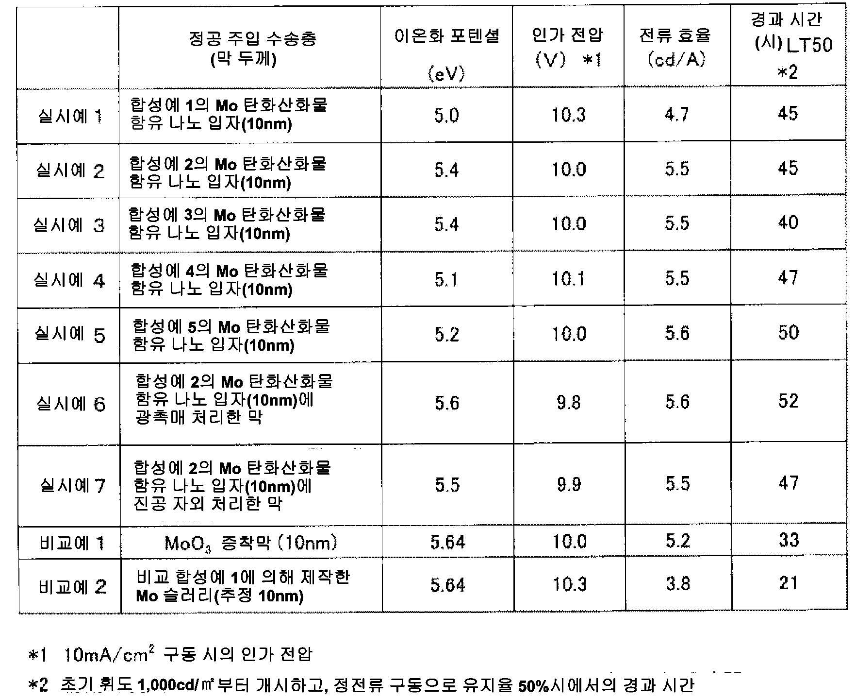
(결과의 정리) (Summary of results)
실시예 1의 소자와 비교예 1 및 비교예 2의 소자를 비교하면, 비교예 1 및 비교예 2의 소자보다, 실시예 1의 소자의 수명이 길고 구동 안정성이 우수한 것을 알았다. 이 결과로부터, MoO3 증착막 및 MoO3 슬러리에 의해 형성한 막보다 몰리브덴 탄화 산화물의 이온화 포텐셜이 적절하거나, 단순한 산화물보다 탄소 원자가 들어감으로써 유기물과의 친화성·밀착성이 향상된 것이, 장수명화에 기여하고 있는 것으로 추측된다.Comparing the elements of Example 1 with the elements of Comparative Example 1 and Comparative Example 2, it was found that the element of Example 1 had a longer life and superior drive stability than the elements of Comparative Example 1 and Comparative Example 2. From these results, the ionization potential of the molybdenum carbonized oxide is more appropriate than the film formed by the MoO 3 deposited film and the MoO 3 slurry, or the carbon atoms are introduced into the film rather than the simple oxide, thereby improving the affinity and adhesion with the organic material. .
또한 MoO3 슬러리를 사용한 비교예 2의 소자에서는, 잉크의 분산성이 나빠, 정공 주입 수송층이 응집되는 경향이 있으므로, 소자는 쇼트하는 경향이 있었다. 이 분산성에 있어서도, 본원 발명의 몰리브덴 탄화 산화물이 더 우수한 것을 알았다.Further, in the device of Comparative Example 2 using the MoO 3 slurry, the dispersibility of the ink was poor and the hole injection transporting layer tended to aggregate, so that the device tended to be short-circuited. It has been found that the molybdenum carbide oxide of the present invention is also superior in this dispersibility.
실시예 2 및 실시예 3의 소자와 실시예 1의 소자를 비교하면, 보호제에 불소 화합물을 사용한 실시예 2 및 실시예 3이 더 이온화 포텐셜이 커지고, 구동 전압이 내려가고 있는 것을 알았다. 보호제를 바꿈으로써 이온화 포텐셜을 컨트롤하여, 소자를 고성능화할 수 있는 것을 알았다.Comparing the elements of Example 2 and Example 3 with those of Example 1, it was found that the ionization potential of Example 2 and Example 3 using a fluorine compound as a protective agent increased and the driving voltage was lowered. It has been found that by changing the protective agent, the ionization potential can be controlled to improve the performance of the device.
실시예 4의 소자와 실시예 1의 소자를 비교하면, 몰리브덴 황화 산화물을 사용한 실시예 4가 더 이온화 포텐셜이 커지고 있어, 소자 특성은 저전압화하여 수명이 길게 되어 있다. 탄소 이외의 화합물과 복합화함으로써 이온화 포텐셜을 컨트롤하여, 소자를 고성능화할 수 있는 것을 알았다.In comparison between the device of Example 4 and the device of Example 1, the ionization potential of Example 4 using molybdenum sulfide oxide is increased, and the device characteristics are lowered and the lifetime is prolonged. It has been found that the ionization potential can be controlled by compounding with a compound other than carbon to improve the performance of the device.
실시예 5의 소자와 실시예 1의 소자를 비교하면, 유기기가 방향환을 포함하는 보호제를 사용한 실시예 5가 더 구동 전압이 내려가 장수명화되는 것을 알았다. 보호제의 유기기를 방향환으로 대체하는 것에 의한, π 전자에 의한 전하 이동성의 향상, 이온화 포텐셜의 증대, 유리 전이 온도의 상승 등의 이유에 의해 소자가 고성능화된 것으로 추측된다. 실시예 5가 실시예 3에 비하여 더 장수명화된 것은, 방향환이 2개 이상 연결된 것에 의해 전하 수송성이 향상된 효과라고 추정된다.Comparing the element of Example 5 with the element of Example 1, it was found that the driving voltage of Example 5 using an organic group containing a protecting group containing an aromatic ring was longer and longer. It is presumed that the device has been improved in performance due to the improvement of charge mobility by π electrons, the increase of the ionization potential and the increase of the glass transition temperature by replacing the organic group of the protecting agent with the aromatic ring. It is presumed that Example 5 is lengthened as compared with Example 3 because charge transportability is improved by connecting two or more aromatic rings.
실시예 6 및 실시예 7의 소자와 실시예 1의 소자를 비교하면, 산화 처리를 실시한 실시예 6 및 실시예 7의 정공 주입 수송층이 더 구동 전압이 내려가 장수명화되는 것을 알았다. 정공 주입 수송층을 적절하게 산화하는 것에 의한, 이온화 포텐셜의 증대 및 나노 입자의 표층이 적절하게 산화되어 화학적 안정성이 향상된 것 등의 이유에 의해 소자가 고성능화된 것으로 추측된다.Comparing the devices of Example 6 and Example 7 with those of Example 1, it was found that the hole injection and transporting layers of Example 6 and Example 7 in which the oxidation treatment was performed further reduced the driving voltage and the lifetime was increased. It is presumed that the device has been improved in performance due to an increase in ionization potential and an appropriate oxidation of the surface layer of the nanoparticles and an improvement in chemical stability by suitably oxidizing the hole injection transport layer.
1: 전이 금속 화합물 함유 나노 입자
10: 전이 금속 및/또는 전이 금속 착체
20: 전이 금속 탄화물
30: 보호제
40: 전이 금속 탄화 산화물
50: 기판
61, 62, 63: 전극
70: 정공 주입 수송층
80: 유기층
90a: 정공 수송층
90b: 정공 주입층
100: 발광층
110: 유기 반도체층
120: 절연층 1: Transition metal compound-containing nanoparticles
10: transition metal and / or transition metal complex
20: transition metal carbide
30: Protective agent
40: transition metal carbide oxide
50: substrate
61, 62, 63: electrodes
70: hole injection and transport layer
80: organic layer
90a: hole transport layer
90b: Hole injection layer
100: light emitting layer
110: organic semiconductor layer
120: insulating layer
Claims (24)
상기 연결기가 수산기, 술폰산기, 술폰아미드기 및 하기 화학식 (1-a) 내지 (1-n)으로 표시되는 관능기에서 선택되는 1종 이상인 것을 특징으로 하는, 전이 금속 화합물 함유 나노 입자.
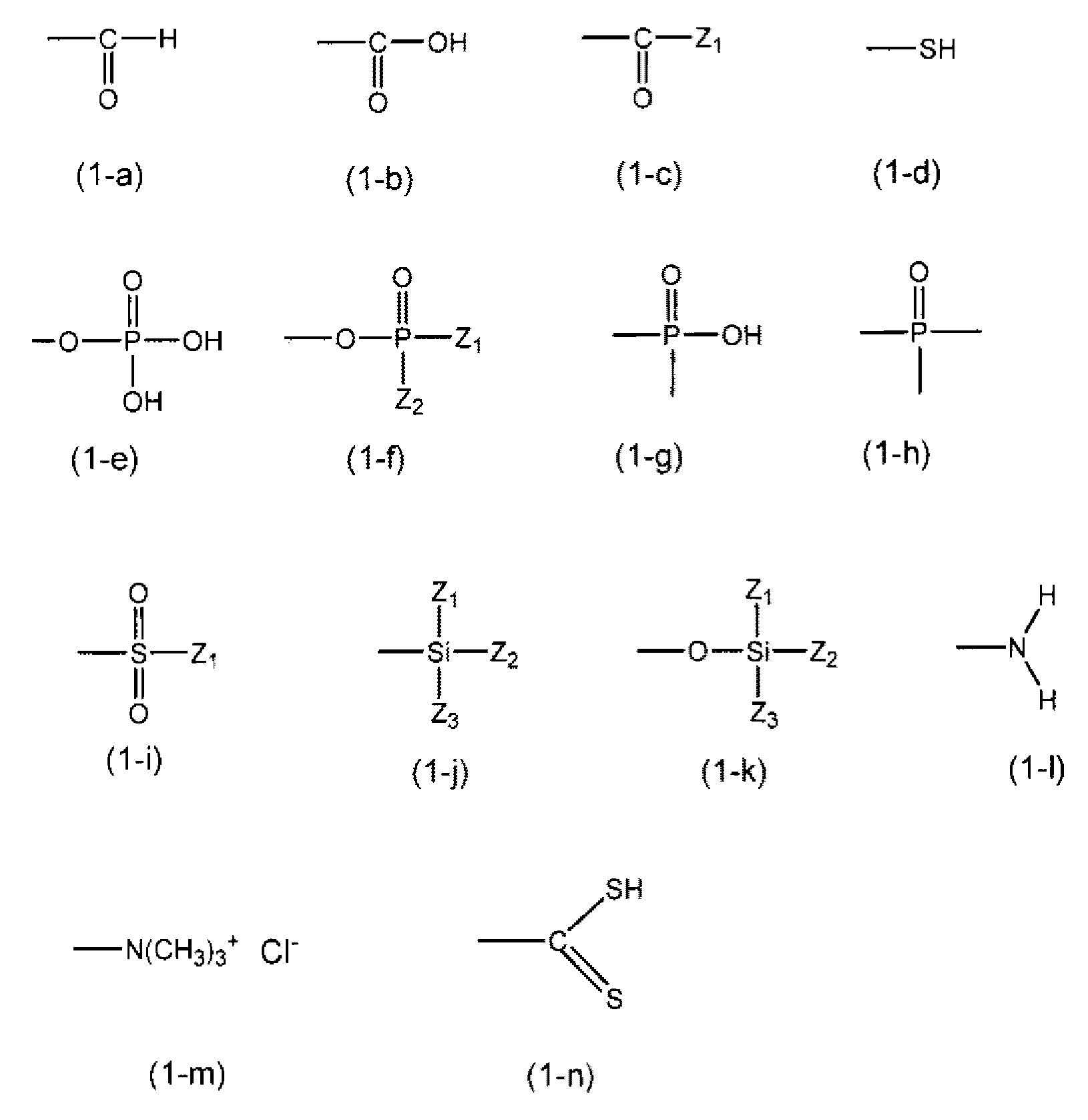
(화학식 중, Z1, Z2 및 Z3는, 각각 독립적으로 할로겐 원자 또는 알콕시기를 나타낸다)A protective group having a linking group and a hydrophobic organic group is connected to the transition metal compound comprising at least one member selected from the group consisting of a transition metal oxide, a transition metal nitride oxide and a transition metal sulfide oxide,
The transition metal compound-containing nanoparticle, wherein the linking group is at least one selected from the group consisting of a hydroxyl group, a sulfonic acid group, a sulfonamide group and functional groups represented by the following formulas (1-a) to (1-n).
(Wherein Z 1 , Z 2 and Z 3 each independently represent a halogen atom or an alkoxy group)
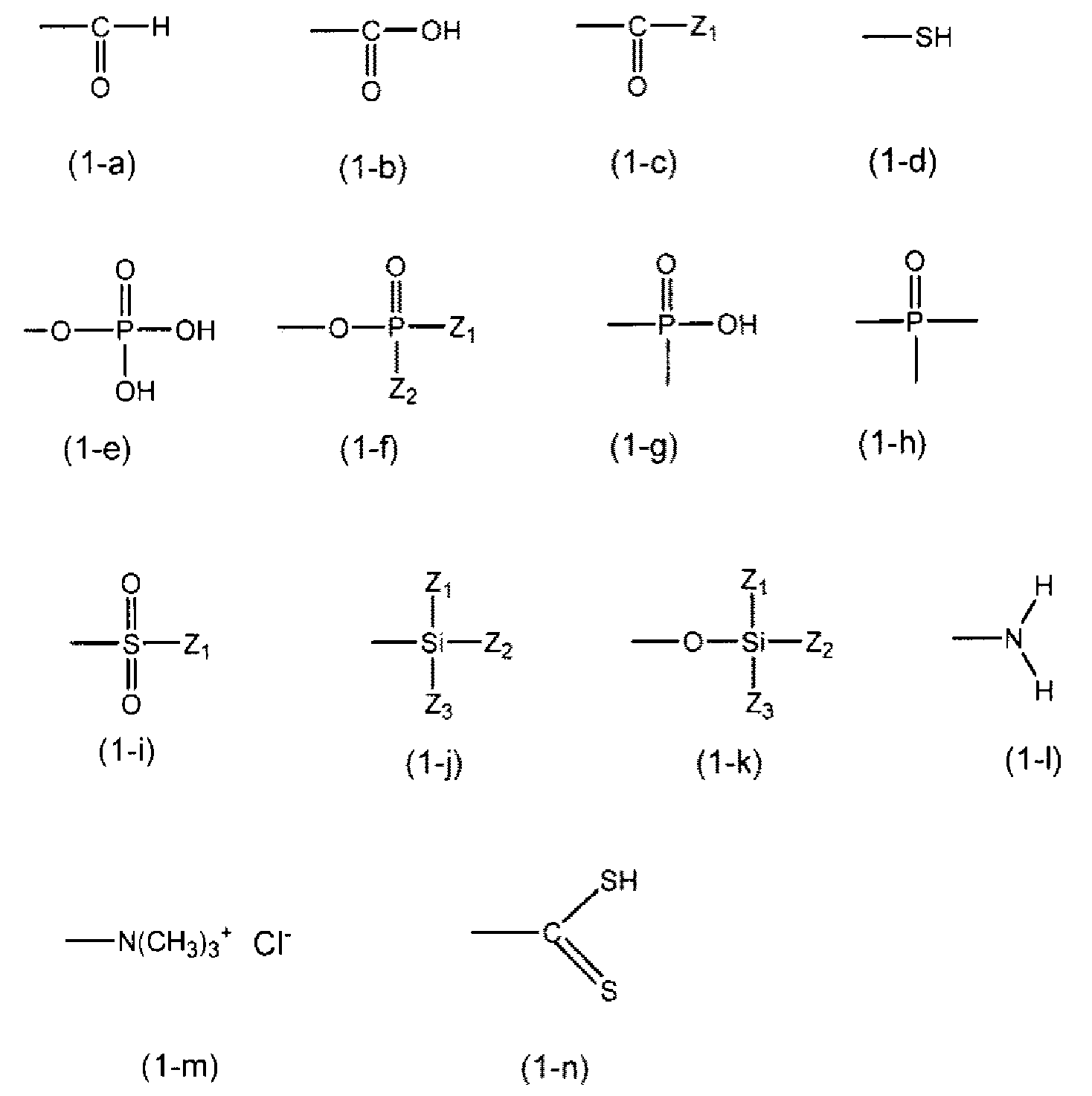
(화학식 중, Z1, Z2 및 Z3은, 각각 독립적으로 할로겐 원자 또는 알콕시기를 나타낸다)The transition metal compound-containing nanoparticles according to claim 1 or 2, wherein the linking group is at least one selected from the functional groups represented by the following formulas (1-a) to (1-n).
(Wherein Z 1 , Z 2 and Z 3 each independently represent a halogen atom or an alkoxy group)
상기 정공 주입 수송층이, 적어도 제1항 또는 제2항에 기재된 전이 금속 화합물 함유 나노 입자를 함유하는 것을 특징으로 하는, 디바이스.A device having two or more electrodes facing each other on a substrate and a hole injecting and transporting layer disposed between two of the electrodes,
Characterized in that the hole-injecting and transporting layer contains the transition metal compound-containing nanoparticles according to any one of claims 1 or 2.
제13항에 기재된 정공 주입 수송층용 잉크를 사용하여, 상기 전극 상의 어느 하나의 층 상에 정공 주입 수송층을 형성하는 공정을 포함하는 것을 특징으로 하는, 디바이스의 제조 방법.A method of manufacturing a device having two or more electrodes facing each other on a substrate and a hole injecting and transporting layer disposed between two of the electrodes,
A method of manufacturing a device, comprising the step of forming a hole injection transport layer on any one of the layers on the electrode using the ink for a hole injection transport layer according to claim 13.
Applications Claiming Priority (3)
| Application Number | Priority Date | Filing Date | Title |
|---|---|---|---|
| JP2009246903 | 2009-10-27 | ||
| JPJP-P-2009-246903 | 2009-10-27 | ||
| PCT/JP2010/069087 WO2011052645A1 (en) | 2009-10-27 | 2010-10-27 | Nanoparticle containing transition metal compound, method for producing same, ink for hole injection/transport layer, device having hole injection/transport layer, and method for producing same |
Related Child Applications (1)
| Application Number | Title | Priority Date | Filing Date |
|---|---|---|---|
| KR1020147010193A Division KR20140054454A (en) | 2009-10-27 | 2010-10-27 | Transition metal compound-containing nanoparticles and a method of producing the same, a device having a hole injection transport layer, a device having a hole injection transport layer, and a method of manufacturing the same |
Publications (2)
| Publication Number | Publication Date |
|---|---|
| KR20120092575A KR20120092575A (en) | 2012-08-21 |
| KR101407880B1 true KR101407880B1 (en) | 2014-06-16 |
Family
ID=43922070
Family Applications (2)
| Application Number | Title | Priority Date | Filing Date |
|---|---|---|---|
| KR1020127007697A Active KR101407880B1 (en) | 2009-10-27 | 2010-10-27 | Nanoparticle containing transition metal compound, method for producing same, ink for hole injection/transport layer, device having hole injection/transport layer, and method for producing same |
| KR1020147010193A Ceased KR20140054454A (en) | 2009-10-27 | 2010-10-27 | Transition metal compound-containing nanoparticles and a method of producing the same, a device having a hole injection transport layer, a device having a hole injection transport layer, and a method of manufacturing the same |
Family Applications After (1)
| Application Number | Title | Priority Date | Filing Date |
|---|---|---|---|
| KR1020147010193A Ceased KR20140054454A (en) | 2009-10-27 | 2010-10-27 | Transition metal compound-containing nanoparticles and a method of producing the same, a device having a hole injection transport layer, a device having a hole injection transport layer, and a method of manufacturing the same |
Country Status (6)
| Country | Link |
|---|---|
| US (1) | US8927099B2 (en) |
| EP (1) | EP2495781B1 (en) |
| JP (2) | JP4905584B2 (en) |
| KR (2) | KR101407880B1 (en) |
| CN (1) | CN102484210B (en) |
| WO (1) | WO2011052645A1 (en) |
Families Citing this family (34)
| Publication number | Priority date | Publication date | Assignee | Title |
|---|---|---|---|---|
| KR101525375B1 (en) | 2008-04-28 | 2015-06-09 | 다이니폰 인사츠 가부시키가이샤 | Material for forming hole injection/transport layer and method for manufacturing the same |
| US8785921B2 (en) * | 2008-04-28 | 2014-07-22 | Dai Nippon Printing Co., Ltd. | Device comprising positive hole injection transport layer, method for producing the same and ink for forming positive hole injection transport layer |
| KR101407880B1 (en) * | 2009-10-27 | 2014-06-16 | 다이니폰 인사츠 가부시키가이샤 | Nanoparticle containing transition metal compound, method for producing same, ink for hole injection/transport layer, device having hole injection/transport layer, and method for producing same |
| JP5783179B2 (en) * | 2010-08-06 | 2015-09-24 | 大日本印刷株式会社 | Transition metal compound-containing nanoparticles and method for producing the same, transition metal compound-containing nanoparticle dispersed ink and method for producing the same, device having a hole injection transport layer, and method for producing the same |
| JP5699323B2 (en) * | 2010-09-30 | 2015-04-08 | 大日本印刷株式会社 | Molybdenum compound nanoparticles and manufacturing method thereof, molybdenum compound nano-particle dispersed ink, device and manufacturing method thereof |
| GB2486202A (en) * | 2010-12-06 | 2012-06-13 | Cambridge Display Tech Ltd | Adhesion layer for solution-processed transition metal oxides on inert metal contacts of organic thin film transistors. |
| KR101465623B1 (en) * | 2012-12-17 | 2014-11-27 | 한국생산기술연구원 | Organic light-emitting diode and method of manufacturing of the same |
| CN103204504B (en) * | 2013-03-07 | 2015-07-29 | 大连理工大学 | A kind of not containing the preparation method of the molybdenum carbide material of non-stoichiometric carbon |
| WO2014186571A1 (en) * | 2013-05-15 | 2014-11-20 | The University Of Akron | Benzoxazole-based materials for vulcanization accelerator applications |
| US10400336B2 (en) | 2014-12-16 | 2019-09-03 | Japan Advanced Institute Of Science And Technology | Oxide precursor, oxide layer, semiconductor element, and electronic device, and method of producing oxide layer and method of producing semiconductor element |
| WO2017014945A1 (en) * | 2015-07-17 | 2017-01-26 | Solvay Usa Inc. | Non-aqueous ink compositions containing metallic nanoparticles suitable for use in organic electronics |
| JP6651310B2 (en) * | 2015-08-28 | 2020-02-19 | 国立研究開発法人産業技術総合研究所 | Nanoparticle and method for producing the same |
| CN105244451B (en) * | 2015-10-16 | 2018-08-14 | Tcl集团股份有限公司 | A kind of light emitting diode with quantum dots and preparation method thereof with mixing HTL |
| CN105552242B (en) * | 2016-01-29 | 2017-05-03 | 苏州大学 | Preparation method of double-charge injection layer for semiconductor device |
| KR102078435B1 (en) | 2016-07-14 | 2020-02-17 | 주식회사 엘지화학 | Organic light emitting diode and manufacturing method of the same |
| US10707531B1 (en) | 2016-09-27 | 2020-07-07 | New Dominion Enterprises Inc. | All-inorganic solvents for electrolytes |
| US10392567B2 (en) | 2016-10-28 | 2019-08-27 | Alliance For Sustainable Energy, Llc | Catalysts and methods for converting biomass to liquid fuels |
| CN106571244A (en) * | 2016-11-02 | 2017-04-19 | 南京工业大学 | Two-dimensional transition group metal carbon (nitrogen) compound and two-dimensional transition group metal sulfide nano composite powder, preparation and application |
| KR102186092B1 (en) | 2016-11-07 | 2020-12-03 | 주식회사 엘지화학 | Coating composition and electroluminescence device comprising the same |
| CN106935719A (en) * | 2017-02-24 | 2017-07-07 | 深圳市华星光电技术有限公司 | A kind of quanta point electroluminescent device and preparation method thereof |
| CN108695411B (en) * | 2017-04-05 | 2019-12-13 | Tcl集团股份有限公司 | Quantum dot light-emitting diode and preparation method thereof |
| CN109427981B (en) * | 2017-08-28 | 2020-11-10 | Tcl科技集团股份有限公司 | QLED device and preparation method thereof |
| CN108305730B (en) * | 2017-08-31 | 2024-06-14 | 中国南方电网有限责任公司超高压输电公司贵阳局 | Ice-coating-preventing insulator |
| CN109427986A (en) * | 2017-09-01 | 2019-03-05 | Tcl集团股份有限公司 | Metal chalcogenide compound of nonmetal doping and its preparation method and application |
| KR102152623B1 (en) * | 2017-10-26 | 2020-09-09 | 한국전자통신연구원 | Display device and manufacturing method thereof |
| CN110534656B (en) * | 2018-05-25 | 2021-03-23 | Tcl科技集团股份有限公司 | Nano material, preparation method and quantum dot light-emitting diode |
| CN109735167B (en) * | 2019-01-08 | 2021-11-05 | 京东方科技集团股份有限公司 | A kind of hole injection layer ink, organic electroluminescent device and manufacturing method thereof |
| JP6838693B2 (en) | 2019-01-31 | 2021-03-03 | 大日本印刷株式会社 | Thin-film masks, electronic device manufacturing methods and electronic devices |
| JP2021192363A (en) | 2020-06-03 | 2021-12-16 | 大日本印刷株式会社 | Electronic device, manufacturing method of electronic device, and vapor deposition mask group |
| JP7788084B2 (en) | 2020-12-28 | 2025-12-18 | 大日本印刷株式会社 | Organic device, mask group, mask, and method for manufacturing organic device |
| JP7788083B2 (en) | 2020-12-28 | 2025-12-18 | 大日本印刷株式会社 | Organic device, mask group, mask, and method for manufacturing organic device |
| US12410507B2 (en) | 2021-06-14 | 2025-09-09 | Dai Nippon Printing Co., Ltd. | Mask group, method of manufacturing organic device and organic device |
| US20220406853A1 (en) | 2021-06-21 | 2022-12-22 | Dai Nippon Printing Co., Ltd. | Organic device, group of masks, mask, and manufacturing method for organic device |
| US12453242B2 (en) | 2021-07-01 | 2025-10-21 | Dai Nippon Printing Co., Ltd. | Organic device and manufacturing method for organic device |
Citations (4)
| Publication number | Priority date | Publication date | Assignee | Title |
|---|---|---|---|---|
| KR20050115737A (en) * | 2004-06-05 | 2005-12-08 | 대한민국(공주대학교총장) | Metal/ceramic nanoparticles having core/shell nanostructure and nanostructured soft-magnets made from the nanoparticles |
| KR20080065296A (en) * | 2005-10-28 | 2008-07-11 | 나노코 테크놀로지스 리미티드 | Controlled Manufacturing Method of Nanoparticle Materials |
| KR20080095522A (en) * | 2007-04-25 | 2008-10-29 | 엘지디스플레이 주식회사 | Organic light emitting device and its manufacturing method |
| KR20080107578A (en) * | 2007-06-07 | 2008-12-11 | 삼성전자주식회사 | Core / Shell Nanocrystals and Manufacturing Method Thereof |
Family Cites Families (42)
| Publication number | Priority date | Publication date | Assignee | Title |
|---|---|---|---|---|
| US4481303A (en) * | 1981-12-23 | 1984-11-06 | The Dow Chemical Company | Electrode material |
| US4695392A (en) * | 1983-05-12 | 1987-09-22 | Advanced Magnetics Inc. | Magnetic particles for use in separations |
| US4554088A (en) * | 1983-05-12 | 1985-11-19 | Advanced Magnetics Inc. | Magnetic particles for use in separations |
| US5260353A (en) * | 1992-10-16 | 1993-11-09 | Kerr-Mcgee Chemical Corporation | Hydrophobicity through metal ion activation |
| JP2824411B2 (en) | 1995-08-25 | 1998-11-11 | 株式会社豊田中央研究所 | Organic thin-film light emitting device |
| JP3748491B2 (en) | 1998-03-27 | 2006-02-22 | 出光興産株式会社 | Organic electroluminescence device |
| JP4058842B2 (en) | 1998-05-13 | 2008-03-12 | 三菱化学株式会社 | Organic electroluminescence device |
| JP2000268973A (en) * | 1999-03-17 | 2000-09-29 | Tdk Corp | Organic EL device |
| CN1150168C (en) * | 2000-08-26 | 2004-05-19 | 暨南大学 | 8-hydroxyquinoline amphiphile complex and preparation method thereof |
| JP2002204012A (en) | 2000-12-28 | 2002-07-19 | Toshiba Corp | Organic transistor and method of manufacturing the same |
| JP4217868B2 (en) * | 2002-05-07 | 2009-02-04 | 大日本印刷株式会社 | Electroluminescent device and manufacturing method thereof |
| US6797380B2 (en) * | 2002-07-31 | 2004-09-28 | General Electric Company | Nanoparticle having an inorganic core |
| JP4519651B2 (en) * | 2002-12-19 | 2010-08-04 | 株式会社半導体エネルギー研究所 | Light emitting device and manufacturing method thereof |
| EP1486551B1 (en) * | 2003-06-13 | 2016-03-16 | Semiconductor Energy Laboratory Co., Ltd. | Light emitting element and light emitting device |
| JP2005093427A (en) * | 2003-08-14 | 2005-04-07 | Mitsubishi Chemicals Corp | Composition for organic electroluminescent device and method for producing organic electroluminescent device |
| JP3748110B1 (en) | 2003-09-26 | 2006-02-22 | 株式会社半導体エネルギー研究所 | LIGHT EMITTING DEVICE AND ELECTRONIC DEVICE USING THE SAME |
| US6818329B1 (en) * | 2003-10-03 | 2004-11-16 | Eastman Kodak Company | Organic electroluminescent devices having a metal sub-layer within a hole-transporting region |
| CN1894808A (en) * | 2003-12-16 | 2007-01-10 | 松下电器产业株式会社 | Organic electroluminescent element and its manufacturing method |
| US20060182993A1 (en) | 2004-08-10 | 2006-08-17 | Mitsubishi Chemical Corporation | Compositions for organic electroluminescent device and organic electroluminescent device |
| US7658991B2 (en) * | 2004-10-21 | 2010-02-09 | University Of Georgia Research Foundation, Inc. | Structures having aligned nanorods and methods of making |
| JP4963172B2 (en) * | 2004-10-22 | 2012-06-27 | 株式会社半導体エネルギー研究所 | Composite material and light emitting device |
| JP2006156981A (en) * | 2004-10-29 | 2006-06-15 | Semiconductor Energy Lab Co Ltd | Composite material, light-emitting element, light-emitting device, and manufacturing method thereof |
| US20070262693A1 (en) | 2004-10-29 | 2007-11-15 | Satoshi Seo | Composite Material, Light-Emitting Element, Light-Emitting Device and Manufacturing Method Thereof |
| JP2006155978A (en) | 2004-11-26 | 2006-06-15 | Seiko Epson Corp | Organic EL device manufacturing method and electronic device |
| CN100388967C (en) * | 2004-12-02 | 2008-05-21 | 鸿富锦精密工业(深圳)有限公司 | Particle dispersion method and its equipment |
| EP1867080A4 (en) * | 2005-03-23 | 2009-08-12 | Semiconductor Energy Lab | COMPOSITE MATERIAL, MATERIAL FOR LIGHT EMITTING ELEMENT, LIGHT EMITTING ELEMENT, LIGHT EMITTING DEVICE, AND ELECTRONIC DEVICE |
| JP5008324B2 (en) * | 2005-03-23 | 2012-08-22 | 株式会社半導体エネルギー研究所 | Composite materials, materials for light-emitting elements, light-emitting elements, light-emitting devices, and electronic devices. |
| CN100358971C (en) * | 2005-10-11 | 2008-01-02 | 友达光电股份有限公司 | Organic light-emitting materials and organic light-emitting devices |
| JP2007287586A (en) | 2006-04-19 | 2007-11-01 | Matsushita Electric Ind Co Ltd | Organic electroluminescent element manufacturing method, organic electroluminescent element, display device and exposure apparatus using the same |
| JP4886352B2 (en) * | 2006-04-25 | 2012-02-29 | パナソニック電工株式会社 | Organic electroluminescence device |
| US20070290604A1 (en) * | 2006-06-16 | 2007-12-20 | Matsushita Electric Industrial Co., Ltd. | Organic electroluminescent device and method of producing the same |
| JP2008041894A (en) | 2006-08-04 | 2008-02-21 | Matsushita Electric Ind Co Ltd | Organic electroluminescent device and manufacturing method thereof |
| DE102006054523B4 (en) * | 2006-11-20 | 2009-07-23 | Novaled Ag | Dithiolene transition metal complexes and selenium-analogous compounds, their use as dopant, organic semiconductive material containing the complexes, and electronic or optoelectronic device containing a complex |
| JP2008153159A (en) * | 2006-12-20 | 2008-07-03 | Dainippon Printing Co Ltd | Organic electroluminescence device and method for producing the same |
| JP2009087781A (en) * | 2007-09-28 | 2009-04-23 | Dainippon Printing Co Ltd | ELECTROLUMINESCENT DEVICE AND METHOD FOR MANUFACTURING THE SAME |
| KR101525375B1 (en) * | 2008-04-28 | 2015-06-09 | 다이니폰 인사츠 가부시키가이샤 | Material for forming hole injection/transport layer and method for manufacturing the same |
| US8785921B2 (en) | 2008-04-28 | 2014-07-22 | Dai Nippon Printing Co., Ltd. | Device comprising positive hole injection transport layer, method for producing the same and ink for forming positive hole injection transport layer |
| KR101652789B1 (en) * | 2009-02-23 | 2016-09-01 | 삼성전자주식회사 | Quantum dot light emitting device having quantum dot multilayer |
| JP5560996B2 (en) * | 2009-07-31 | 2014-07-30 | 大日本印刷株式会社 | Device material for hole injection transport layer, ink for forming hole injection transport layer, device having hole injection transport layer, and method for producing the same |
| JP5531843B2 (en) * | 2009-07-31 | 2014-06-25 | 大日本印刷株式会社 | Device material for hole injection transport layer, ink for forming hole injection transport layer, device having hole injection transport layer, and method for producing the same |
| KR101407880B1 (en) * | 2009-10-27 | 2014-06-16 | 다이니폰 인사츠 가부시키가이샤 | Nanoparticle containing transition metal compound, method for producing same, ink for hole injection/transport layer, device having hole injection/transport layer, and method for producing same |
| JP4798282B2 (en) * | 2009-10-27 | 2011-10-19 | 大日本印刷株式会社 | Device having hole injection transport layer, method for producing the same, and ink for forming hole injection transport layer |
-
2010
- 2010-10-27 KR KR1020127007697A patent/KR101407880B1/en active Active
- 2010-10-27 JP JP2010241015A patent/JP4905584B2/en active Active
- 2010-10-27 EP EP10826777.4A patent/EP2495781B1/en not_active Not-in-force
- 2010-10-27 US US13/391,652 patent/US8927099B2/en not_active Expired - Fee Related
- 2010-10-27 CN CN201080040121.9A patent/CN102484210B/en active Active
- 2010-10-27 KR KR1020147010193A patent/KR20140054454A/en not_active Ceased
- 2010-10-27 WO PCT/JP2010/069087 patent/WO2011052645A1/en not_active Ceased
-
2011
- 2011-03-22 JP JP2011062726A patent/JP5655656B2/en active Active
Patent Citations (4)
| Publication number | Priority date | Publication date | Assignee | Title |
|---|---|---|---|---|
| KR20050115737A (en) * | 2004-06-05 | 2005-12-08 | 대한민국(공주대학교총장) | Metal/ceramic nanoparticles having core/shell nanostructure and nanostructured soft-magnets made from the nanoparticles |
| KR20080065296A (en) * | 2005-10-28 | 2008-07-11 | 나노코 테크놀로지스 리미티드 | Controlled Manufacturing Method of Nanoparticle Materials |
| KR20080095522A (en) * | 2007-04-25 | 2008-10-29 | 엘지디스플레이 주식회사 | Organic light emitting device and its manufacturing method |
| KR20080107578A (en) * | 2007-06-07 | 2008-12-11 | 삼성전자주식회사 | Core / Shell Nanocrystals and Manufacturing Method Thereof |
Also Published As
| Publication number | Publication date |
|---|---|
| EP2495781A4 (en) | 2017-04-12 |
| CN102484210A (en) | 2012-05-30 |
| JP5655656B2 (en) | 2015-01-21 |
| KR20120092575A (en) | 2012-08-21 |
| WO2011052645A1 (en) | 2011-05-05 |
| EP2495781A1 (en) | 2012-09-05 |
| KR20140054454A (en) | 2014-05-08 |
| CN102484210B (en) | 2016-01-20 |
| US20120146010A1 (en) | 2012-06-14 |
| EP2495781B1 (en) | 2018-12-05 |
| JP2011173788A (en) | 2011-09-08 |
| US8927099B2 (en) | 2015-01-06 |
| JP2011119681A (en) | 2011-06-16 |
| JP4905584B2 (en) | 2012-03-28 |
Similar Documents
| Publication | Publication Date | Title |
|---|---|---|
| KR101407880B1 (en) | Nanoparticle containing transition metal compound, method for producing same, ink for hole injection/transport layer, device having hole injection/transport layer, and method for producing same | |
| KR101508806B1 (en) | Device having hole injection transport layer, method for production thereof, and ink for formation of hole injection transport layer | |
| KR101599575B1 (en) | Device having hole injection/transport layer, method for producing same, and ink for forming hole injection/transport layer | |
| KR101509283B1 (en) | Device having hole injection/transport layer, method for manufacturing the same, and ink for forming hole injection/transport layer | |
| JP5783179B2 (en) | Transition metal compound-containing nanoparticles and method for producing the same, transition metal compound-containing nanoparticle dispersed ink and method for producing the same, device having a hole injection transport layer, and method for producing the same | |
| JP5699323B2 (en) | Molybdenum compound nanoparticles and manufacturing method thereof, molybdenum compound nano-particle dispersed ink, device and manufacturing method thereof | |
| JP2017098172A (en) | Method for producing charge transport layer forming ink, device producing method |
Legal Events
| Date | Code | Title | Description |
|---|---|---|---|
| PA0105 | International application |
Patent event date: 20120326 Patent event code: PA01051R01D Comment text: International Patent Application |
|
| A201 | Request for examination | ||
| AMND | Amendment | ||
| PA0201 | Request for examination |
Patent event code: PA02012R01D Patent event date: 20120615 Comment text: Request for Examination of Application |
|
| PG1501 | Laying open of application | ||
| E902 | Notification of reason for refusal | ||
| PE0902 | Notice of grounds for rejection |
Comment text: Notification of reason for refusal Patent event date: 20130923 Patent event code: PE09021S01D |
|
| AMND | Amendment | ||
| E601 | Decision to refuse application | ||
| PE0601 | Decision on rejection of patent |
Patent event date: 20140317 Comment text: Decision to Refuse Application Patent event code: PE06012S01D Patent event date: 20130923 Comment text: Notification of reason for refusal Patent event code: PE06011S01I |
|
| A107 | Divisional application of patent | ||
| AMND | Amendment | ||
| PA0104 | Divisional application for international application |
Comment text: Divisional Application for International Patent Patent event code: PA01041R01D Patent event date: 20140416 |
|
| PX0901 | Re-examination |
Patent event code: PX09011S01I Patent event date: 20140317 Comment text: Decision to Refuse Application Patent event code: PX09012R01I Patent event date: 20131125 Comment text: Amendment to Specification, etc. Patent event code: PX09012R01I Patent event date: 20120615 Comment text: Amendment to Specification, etc. |
|
| PX0701 | Decision of registration after re-examination |
Patent event date: 20140429 Comment text: Decision to Grant Registration Patent event code: PX07013S01D Patent event date: 20140416 Comment text: Amendment to Specification, etc. Patent event code: PX07012R01I Patent event date: 20140317 Comment text: Decision to Refuse Application Patent event code: PX07011S01I Patent event date: 20131125 Comment text: Amendment to Specification, etc. Patent event code: PX07012R01I Patent event date: 20120615 Comment text: Amendment to Specification, etc. Patent event code: PX07012R01I |
|
| X701 | Decision to grant (after re-examination) | ||
| GRNT | Written decision to grant | ||
| PR0701 | Registration of establishment |
Comment text: Registration of Establishment Patent event date: 20140609 Patent event code: PR07011E01D |
|
| PR1002 | Payment of registration fee |
Payment date: 20140609 End annual number: 3 Start annual number: 1 |
|
| PG1601 | Publication of registration | ||
| FPAY | Annual fee payment |
Payment date: 20170602 Year of fee payment: 4 |
|
| PR1001 | Payment of annual fee |
Payment date: 20170602 Start annual number: 4 End annual number: 4 |
|
| PR1001 | Payment of annual fee |
Payment date: 20220530 Start annual number: 9 End annual number: 9 |