KR101401527B1 - Light-emitting device and electronic device - Google Patents
Light-emitting device and electronic device Download PDFInfo
- Publication number
- KR101401527B1 KR101401527B1 KR1020080025841A KR20080025841A KR101401527B1 KR 101401527 B1 KR101401527 B1 KR 101401527B1 KR 1020080025841 A KR1020080025841 A KR 1020080025841A KR 20080025841 A KR20080025841 A KR 20080025841A KR 101401527 B1 KR101401527 B1 KR 101401527B1
- Authority
- KR
- South Korea
- Prior art keywords
- light emitting
- organic compound
- layer
- emitting layer
- light
- Prior art date
- Legal status (The legal status is an assumption and is not a legal conclusion. Google has not performed a legal analysis and makes no representation as to the accuracy of the status listed.)
- Expired - Fee Related
Links
- 0 CC*[C@](CC(N)=C[C@]([C@@](C)[C@@](CCCOC(C)O)C(C)=C)C1CCCCC1)C1C=C[C@@]2(C)N[C@](C(C=C3)=CCC3OC(C)O)C(C3C=CC=CC3)=CNC2CC1 Chemical compound CC*[C@](CC(N)=C[C@]([C@@](C)[C@@](CCCOC(C)O)C(C)=C)C1CCCCC1)C1C=C[C@@]2(C)N[C@](C(C=C3)=CCC3OC(C)O)C(C3C=CC=CC3)=CNC2CC1 0.000 description 1
Images


Classifications
-
- H—ELECTRICITY
- H05—ELECTRIC TECHNIQUES NOT OTHERWISE PROVIDED FOR
- H05B—ELECTRIC HEATING; ELECTRIC LIGHT SOURCES NOT OTHERWISE PROVIDED FOR; CIRCUIT ARRANGEMENTS FOR ELECTRIC LIGHT SOURCES, IN GENERAL
- H05B33/00—Electroluminescent light sources
- H05B33/12—Light sources with substantially two-dimensional radiating surfaces
- H05B33/14—Light sources with substantially two-dimensional radiating surfaces characterised by the chemical or physical composition or the arrangement of the electroluminescent material, or by the simultaneous addition of the electroluminescent material in or onto the light source
-
- C—CHEMISTRY; METALLURGY
- C09—DYES; PAINTS; POLISHES; NATURAL RESINS; ADHESIVES; COMPOSITIONS NOT OTHERWISE PROVIDED FOR; APPLICATIONS OF MATERIALS NOT OTHERWISE PROVIDED FOR
- C09K—MATERIALS FOR MISCELLANEOUS APPLICATIONS, NOT PROVIDED FOR ELSEWHERE
- C09K11/00—Luminescent, e.g. electroluminescent, chemiluminescent materials
- C09K11/06—Luminescent, e.g. electroluminescent, chemiluminescent materials containing organic luminescent materials
-
- H—ELECTRICITY
- H05—ELECTRIC TECHNIQUES NOT OTHERWISE PROVIDED FOR
- H05B—ELECTRIC HEATING; ELECTRIC LIGHT SOURCES NOT OTHERWISE PROVIDED FOR; CIRCUIT ARRANGEMENTS FOR ELECTRIC LIGHT SOURCES, IN GENERAL
- H05B33/00—Electroluminescent light sources
- H05B33/12—Light sources with substantially two-dimensional radiating surfaces
- H05B33/18—Light sources with substantially two-dimensional radiating surfaces characterised by the nature or concentration of the activator
-
- H—ELECTRICITY
- H05—ELECTRIC TECHNIQUES NOT OTHERWISE PROVIDED FOR
- H05B—ELECTRIC HEATING; ELECTRIC LIGHT SOURCES NOT OTHERWISE PROVIDED FOR; CIRCUIT ARRANGEMENTS FOR ELECTRIC LIGHT SOURCES, IN GENERAL
- H05B33/00—Electroluminescent light sources
- H05B33/12—Light sources with substantially two-dimensional radiating surfaces
- H05B33/20—Light sources with substantially two-dimensional radiating surfaces characterised by the chemical or physical composition or the arrangement of the material in which the electroluminescent material is embedded
-
- H—ELECTRICITY
- H10—SEMICONDUCTOR DEVICES; ELECTRIC SOLID-STATE DEVICES NOT OTHERWISE PROVIDED FOR
- H10K—ORGANIC ELECTRIC SOLID-STATE DEVICES
- H10K50/00—Organic light-emitting devices
- H10K50/10—OLEDs or polymer light-emitting diodes [PLED]
- H10K50/11—OLEDs or polymer light-emitting diodes [PLED] characterised by the electroluminescent [EL] layers
-
- H—ELECTRICITY
- H10—SEMICONDUCTOR DEVICES; ELECTRIC SOLID-STATE DEVICES NOT OTHERWISE PROVIDED FOR
- H10K—ORGANIC ELECTRIC SOLID-STATE DEVICES
- H10K50/00—Organic light-emitting devices
- H10K50/10—OLEDs or polymer light-emitting diodes [PLED]
- H10K50/14—Carrier transporting layers
-
- H—ELECTRICITY
- H10—SEMICONDUCTOR DEVICES; ELECTRIC SOLID-STATE DEVICES NOT OTHERWISE PROVIDED FOR
- H10K—ORGANIC ELECTRIC SOLID-STATE DEVICES
- H10K59/00—Integrated devices, or assemblies of multiple devices, comprising at least one organic light-emitting element covered by group H10K50/00
- H10K59/30—Devices specially adapted for multicolour light emission
- H10K59/35—Devices specially adapted for multicolour light emission comprising red-green-blue [RGB] subpixels
-
- H—ELECTRICITY
- H10—SEMICONDUCTOR DEVICES; ELECTRIC SOLID-STATE DEVICES NOT OTHERWISE PROVIDED FOR
- H10K—ORGANIC ELECTRIC SOLID-STATE DEVICES
- H10K85/00—Organic materials used in the body or electrodes of devices covered by this subclass
- H10K85/60—Organic compounds having low molecular weight
- H10K85/631—Amine compounds having at least two aryl rest on at least one amine-nitrogen atom, e.g. triphenylamine
- H10K85/633—Amine compounds having at least two aryl rest on at least one amine-nitrogen atom, e.g. triphenylamine comprising polycyclic condensed aromatic hydrocarbons as substituents on the nitrogen atom
-
- H—ELECTRICITY
- H10—SEMICONDUCTOR DEVICES; ELECTRIC SOLID-STATE DEVICES NOT OTHERWISE PROVIDED FOR
- H10K—ORGANIC ELECTRIC SOLID-STATE DEVICES
- H10K85/00—Organic materials used in the body or electrodes of devices covered by this subclass
- H10K85/60—Organic compounds having low molecular weight
- H10K85/631—Amine compounds having at least two aryl rest on at least one amine-nitrogen atom, e.g. triphenylamine
- H10K85/636—Amine compounds having at least two aryl rest on at least one amine-nitrogen atom, e.g. triphenylamine comprising heteroaromatic hydrocarbons as substituents on the nitrogen atom
-
- H—ELECTRICITY
- H10—SEMICONDUCTOR DEVICES; ELECTRIC SOLID-STATE DEVICES NOT OTHERWISE PROVIDED FOR
- H10K—ORGANIC ELECTRIC SOLID-STATE DEVICES
- H10K85/00—Organic materials used in the body or electrodes of devices covered by this subclass
- H10K85/60—Organic compounds having low molecular weight
- H10K85/649—Aromatic compounds comprising a hetero atom
- H10K85/657—Polycyclic condensed heteroaromatic hydrocarbons
- H10K85/6572—Polycyclic condensed heteroaromatic hydrocarbons comprising only nitrogen in the heteroaromatic polycondensed ring system, e.g. phenanthroline or carbazole
-
- C—CHEMISTRY; METALLURGY
- C09—DYES; PAINTS; POLISHES; NATURAL RESINS; ADHESIVES; COMPOSITIONS NOT OTHERWISE PROVIDED FOR; APPLICATIONS OF MATERIALS NOT OTHERWISE PROVIDED FOR
- C09K—MATERIALS FOR MISCELLANEOUS APPLICATIONS, NOT PROVIDED FOR ELSEWHERE
- C09K2211/00—Chemical nature of organic luminescent or tenebrescent compounds
- C09K2211/10—Non-macromolecular compounds
- C09K2211/1003—Carbocyclic compounds
- C09K2211/1011—Condensed systems
-
- C—CHEMISTRY; METALLURGY
- C09—DYES; PAINTS; POLISHES; NATURAL RESINS; ADHESIVES; COMPOSITIONS NOT OTHERWISE PROVIDED FOR; APPLICATIONS OF MATERIALS NOT OTHERWISE PROVIDED FOR
- C09K—MATERIALS FOR MISCELLANEOUS APPLICATIONS, NOT PROVIDED FOR ELSEWHERE
- C09K2211/00—Chemical nature of organic luminescent or tenebrescent compounds
- C09K2211/10—Non-macromolecular compounds
- C09K2211/1018—Heterocyclic compounds
- C09K2211/1025—Heterocyclic compounds characterised by ligands
- C09K2211/1029—Heterocyclic compounds characterised by ligands containing one nitrogen atom as the heteroatom
-
- C—CHEMISTRY; METALLURGY
- C09—DYES; PAINTS; POLISHES; NATURAL RESINS; ADHESIVES; COMPOSITIONS NOT OTHERWISE PROVIDED FOR; APPLICATIONS OF MATERIALS NOT OTHERWISE PROVIDED FOR
- C09K—MATERIALS FOR MISCELLANEOUS APPLICATIONS, NOT PROVIDED FOR ELSEWHERE
- C09K2211/00—Chemical nature of organic luminescent or tenebrescent compounds
- C09K2211/10—Non-macromolecular compounds
- C09K2211/1018—Heterocyclic compounds
- C09K2211/1025—Heterocyclic compounds characterised by ligands
- C09K2211/1044—Heterocyclic compounds characterised by ligands containing two nitrogen atoms as heteroatoms
-
- C—CHEMISTRY; METALLURGY
- C09—DYES; PAINTS; POLISHES; NATURAL RESINS; ADHESIVES; COMPOSITIONS NOT OTHERWISE PROVIDED FOR; APPLICATIONS OF MATERIALS NOT OTHERWISE PROVIDED FOR
- C09K—MATERIALS FOR MISCELLANEOUS APPLICATIONS, NOT PROVIDED FOR ELSEWHERE
- C09K2211/00—Chemical nature of organic luminescent or tenebrescent compounds
- C09K2211/18—Metal complexes
- C09K2211/185—Metal complexes of the platinum group, i.e. Os, Ir, Pt, Ru, Rh or Pd
-
- H—ELECTRICITY
- H10—SEMICONDUCTOR DEVICES; ELECTRIC SOLID-STATE DEVICES NOT OTHERWISE PROVIDED FOR
- H10K—ORGANIC ELECTRIC SOLID-STATE DEVICES
- H10K2101/00—Properties of the organic materials covered by group H10K85/00
- H10K2101/10—Triplet emission
-
- H—ELECTRICITY
- H10—SEMICONDUCTOR DEVICES; ELECTRIC SOLID-STATE DEVICES NOT OTHERWISE PROVIDED FOR
- H10K—ORGANIC ELECTRIC SOLID-STATE DEVICES
- H10K2101/00—Properties of the organic materials covered by group H10K85/00
- H10K2101/30—Highest occupied molecular orbital [HOMO], lowest unoccupied molecular orbital [LUMO] or Fermi energy values
-
- H—ELECTRICITY
- H10—SEMICONDUCTOR DEVICES; ELECTRIC SOLID-STATE DEVICES NOT OTHERWISE PROVIDED FOR
- H10K—ORGANIC ELECTRIC SOLID-STATE DEVICES
- H10K85/00—Organic materials used in the body or electrodes of devices covered by this subclass
- H10K85/30—Coordination compounds
- H10K85/321—Metal complexes comprising a group IIIA element, e.g. Tris (8-hydroxyquinoline) gallium [Gaq3]
- H10K85/324—Metal complexes comprising a group IIIA element, e.g. Tris (8-hydroxyquinoline) gallium [Gaq3] comprising aluminium, e.g. Alq3
-
- H—ELECTRICITY
- H10—SEMICONDUCTOR DEVICES; ELECTRIC SOLID-STATE DEVICES NOT OTHERWISE PROVIDED FOR
- H10K—ORGANIC ELECTRIC SOLID-STATE DEVICES
- H10K85/00—Organic materials used in the body or electrodes of devices covered by this subclass
- H10K85/30—Coordination compounds
- H10K85/341—Transition metal complexes, e.g. Ru(II)polypyridine complexes
- H10K85/342—Transition metal complexes, e.g. Ru(II)polypyridine complexes comprising iridium
Landscapes
- Chemical & Material Sciences (AREA)
- Physics & Mathematics (AREA)
- Engineering & Computer Science (AREA)
- Materials Engineering (AREA)
- Optics & Photonics (AREA)
- Organic Chemistry (AREA)
- Spectroscopy & Molecular Physics (AREA)
- Electroluminescent Light Sources (AREA)
Abstract
특성이 우수한 발광장치를 제공하는 것을 과제로 한다. 또한 특성이 우수한 발광장치를 가지는 전자기기를 제공하는 것을 과제로 한다. 서로 발광색이 다른 제1 발광소자, 제2 발광소자 및 제3 발광소자를 적어도 가지고, 제1 발광소자는, 제1 양극과 제1 음극의 사이에, 제1 발광층과 제2 발광층을 가지고, 제1 발광층은, 제1 발광성이 높은 물질과, 제1 유기 화합물을 가지고, 제2 발광층은, 제1 발광성이 높은 물질과, 제2 유기 화합물을 가지고, 제1 발광층은 제2 발광층의 제1 양극측에 접해서 설치되는 발광소자이며, 제1 유기 화합물은 정공수송성 유기 화합물이며, 제2 유기 화합물은 전자수송성 유기 화합물이며, 제2 발광소자는, 제2 양극과 제2 음극 사이에, 제3 발광층과 캐리어의 이동을 제어하는 층을 가지고, 제3 발광층은, 제2 발광성이 높은 물질을 가지고, 캐리어의 이동을 제어하는 층은, 제3 유기 화합물과, 제4 유기 화합물을 가지고, 캐리어의 이동을 제어하는 층은, 발광층과 제2 음극 사이에 설치되어 있고, 제3 유기 화합물은, 전자수송성 유기 화합물이며, 제4 유기 화합물은, 전자 트랩성 유기 화합물이며, 캐리어의 이동을 제어하는 층에 있어서, 제4 유기 화합물보다도 제3 유기 화합물이 많이 포함되어 있고, 제3 발광소자는, 제3 양극과 제3 음극의 사이에, 제4 발광층을 가지고, 제4 발광층은, 제5 유기 화합물과, 제6 유기 화합물과, 제3 발광성이 높은 물질을 포함하고, 제5 유기 화합물은 정공수송성 유기 화합물이며, 제6 유기 화합물은 전자수송성 유기 화합물이며, 제3 발광성이 높은 물질은, 인광을 발광하는 물질인 발광장치를 제공한다.

발광장치, 전자기기, 유기 화합물, 전자, 정공
And to provide a light emitting device having excellent characteristics. It is another object of the present invention to provide an electronic apparatus having a light emitting device having excellent characteristics. Wherein the first light emitting element has a first light emitting layer and a second light emitting layer between the first anode and the first cathode, The first light emitting layer has a substance having a first light emitting property and a first organic compound and the second light emitting layer has a substance having a first light emitting property and a second organic compound, And the second organic compound is an electron transporting organic compound, and the second light emitting element is a light emitting element provided between the second anode and the second cathode, and the third organic compound is a hole transporting organic compound, The third light-emitting layer has a substance having a high second light-emitting property, the layer controlling the movement of the carrier has a third organic compound and a fourth organic compound, and the layer of the carrier The layer for controlling the movement is a layer in which the light- , The third organic compound is an electron transporting organic compound, the fourth organic compound is an electron trapping organic compound, and the third organic compound And the third light emitting element has a fourth light emitting layer between the third anode and the third cathode and the fourth light emitting layer includes the fifth organic compound and the sixth organic compound and the third light emitting element The fifth organic compound is a hole transporting organic compound, the sixth organic compound is an electron transporting organic compound, and the third luminescent material is a material for emitting phosphorescence.
Light emitting device, electronic device, organic compound, electron, hole
Description
본 발명은 일렉트로루미네선스를 이용한 발광소자를 가지는 발광장치 및 전자기기에 관한 것이다.The present invention relates to a light emitting device and an electronic device having a light emitting device using electroluminescence.
최근, 일렉트로루미네선스(electroluminescence)를 이용한 발광소자의 연구 개발이 활발히 이루어지고 있다. 이러한 발광소자의 기본적인 구성은, 한 쌍의 전극 간에 발광성 물질(이하, 발광물질이라고도 한다)을 개재한 것이다. 이 소자에 전압을 인가함으로써, 발광성 물질로부터의 발광을 얻을 수 있다.Recently, research and development of a light emitting device using electroluminescence have been actively conducted. The basic structure of such a light-emitting element is a light-emitting material (hereinafter also referred to as a light-emitting material) interposed between a pair of electrodes. By applying a voltage to this device, light emission from the luminescent material can be obtained.
이러한 발광소자는 자발광형이기 때문에, 액정 디스플레이에 비해 화소의 시인성이 높고, 백라이트를 필요로 하지 않는 등의 이점이 있어, 플랫 패널 디스플레이 소자로서 적합하다고 여겨지고 있다. 또한 이러한 발광소자는, 초경량으로 제조할 수 있는 것도 큰 이점이다. 또한 상당히 응답 속도가 빠른 것도 특징의 하나다.Since such a light emitting device is of a self-emission type, it has advantages such as high visibility of a pixel and no need of a backlight compared to a liquid crystal display, and it is considered to be suitable as a flat panel display device. Further, such a light-emitting element is also advantageous in that it can be manufactured with a light weight. Also, it is one of the features that the response speed is considerably high.
또한 이러한 발광소자는 막형으로 형성할 수 있기 때문에, 대면적의 소자를 형성함으로써, 면형의 발광을 용이하게 얻을 수 있다. 이는 백열전구나 LED로 대표되는 점광원, 혹은 형광등으로 대표되는 선광원으로는 얻기 어려운 특색이기 때문에, 조명 등에 응용할 수 있는 면광원으로서의 이용 가치도 높다.Further, since such a light-emitting element can be formed in a film-like form, by forming a large-area element, light emission in a planar form can be easily obtained. This is a characteristic that is difficult to obtain as a point light source typified by an incandescent lamp or an LED, or a point light source typified by a fluorescent lamp, and thus has a high use value as a surface light source applicable to illumination and the like.
일렉트로루미네선스를 이용한 발광소자는, 발광성 물질이 유기 화합물인지, 무기 화합물인지에 따라 크게 나누어진다.A light emitting device using electroluminescence is largely divided depending on whether the luminescent material is an organic compound or an inorganic compound.
발광성 물질이 유기 화합물인 경우, 발광소자에 전압을 인가함으로써, 한 쌍의 전극으로부터 전자 및 정공이 각각 발광성 유기 화합물을 포함한 층에 주입되어, 전류가 흐른다. 그리고, 그들 캐리어(전자 및 정공)가 재결합함으로써, 발광성 유기 화합물이 여기상태를 형성하고, 그 여기상태가 기저상태로 되돌아올 때에 발광한다. 이러한 메커니즘으로부터, 이러한 발광소자는, 전류 여기형 발광소자라고 불린다.When the luminescent material is an organic compound, by applying a voltage to the luminescent element, electrons and holes from the pair of electrodes are injected into the layer containing the luminescent organic compound, respectively, and a current flows. Then, the carriers (electrons and holes) recombine to emit light when the luminous organic compound forms an excited state and the excited state returns to the ground state. From such a mechanism, such a light-emitting element is called a current-excited light-emitting element.
이때, 유기 화합물이 형성하는 여기상태의 종류로는, 단일항 여기상태와 삼중항 여기상태가 가능한데, 단일항 여기상태로부터의 발광이 형광, 삼중항 여기상태로부터의 발광이 인광이라고 불리고 있다.At this time, as a kind of the excited state formed by the organic compound, a singlet excited state and a triplet excited state are possible. Light emission from singlet excited state is called fluorescence, and light emission from triplet excited state is called phosphorescence.
이러한 발광소자에 있어서는, 그 소자특성을 향상시키는 데에, 재료에 의존한 문제가 많고, 이것들을 극복하기 위해서 소자구조의 개량이나 재료개발 등이 이루어지고 있다.In such a light-emitting device, there are many problems depending on the materials in order to improve the device characteristics. In order to overcome these problems, improvement of the device structure and material development have been carried out.
예를 들면 발광소자를 디스플레이 소자로 사용할 경우, 각 색의 발광소자의 특성이 다른 것에 의해, 디스플레이로서의 성능이 손상된다는 문제가 있었다.For example, when a light emitting element is used as a display element, there is a problem that the performance as a display is impaired due to the different characteristics of the light emitting element of each color.
이러한 문제를 해결하기 위해서, 특허문헌 1에서는, 적색으로 발광하는 EL소자의 발광층으로서 트리플릿(삼중항) 화합물을 사용하고, 녹색으로 발광하는 EL소자의 발광층 및 청색으로 발광하는 EL소자의 발광층에 싱글릿(단일항) 화합 물을 사용한 발광장치를 개시하고 있다.In order to solve such a problem,
[특허문헌 1] 일본국 공개특허공보 특개 2002-62824호[Patent Document 1] Japanese Patent Application Laid-Open No. 2002-62824
그러나 발광장치로서의 특성은 아직 개선의 여지가 있어, 보다 좋은 특성을 지니는 발광장치의 개발이 기대되고 있다.However, the characteristics as a light emitting device have still room for improvement, and development of a light emitting device having better characteristics is expected.
이에 따라, 본 발명은, 특성이 우수한 발광장치를 제공하는 것을 과제로 한다. 또한 특성이 우수한 발광장치를 가지는 전자기기를 제공하는 것을 과제로 한다.Accordingly, it is an object of the present invention to provide a light emitting device having excellent characteristics. It is another object of the present invention to provide an electronic apparatus having a light emitting device having excellent characteristics.
본 발명은 발광색이 다른 복수의 발광소자를 가지고 다색 표시를 행하는 발광장치로서, 그 발광소자의 발광층을 포함한 구성이 발광색마다 다른 것을 요지로 한다.The present invention relates to a light emitting device for performing multicolor display with a plurality of light emitting elements having different luminescent colors, wherein the constitution including the light emitting layer of the light emitting element differs for each luminescent color.
구체적으로는, 컬러 표시를 행하는 발광장치에 있어서, 청색 발광소자에 대해서는, 이하의 구성인 것이 바람직하다.Specifically, in a light emitting device that performs color display, it is preferable that the blue light emitting element has the following configuration.
본 발명자들은, 청색 발광소자에 있어서의 발광층의 실질적인 발광 영역을, 상기 발광층의 중앙 부근으로 제어하는 것, 즉, 발광 영역을, 발광층과 정공수송층의 계면이나 발광층과 전자수송층의 계면이 아닌, 발광층의 중앙 부근이 되도록, 캐리어 수송 특성이 다른 층을 조합해서 발광층을 구성함으로써, 긴 수명의 청색 발광소자를 실현한다는 것을 알아냈다.The present inventors have found that it is possible to control the substantial luminescent region of the luminescent layer in the blue luminescent element to the vicinity of the center of the luminescent layer, that is, to control the luminescent region in the luminescent layer, not at the interface of the luminescent layer and the hole- It has been found that a blue light emitting element with a long lifetime is realized by forming a light emitting layer by combining layers having different carrier transporting characteristics so as to be in the vicinity of the center of the light emitting layer.
따라서, 양극과 음극 사이에, 제1 발광층과 제2 발광층을 가지고, 제1 발광 층은, 제1 유기 화합물과, 정공수송성 유기 화합물을 가지고, 제2 발광층은, 제1 유기 화합물과, 전자수송성 유기 화합물을 가지고, 제1 발광층은, 제2 발광층의 양극측에 접해서 설치되는 구성인 것이 바람직하다.Therefore, it is preferable that the organic EL device has a first light emitting layer and a second light emitting layer between the anode and the cathode, the first light emitting layer has the first organic compound and the hole transporting organic compound, It is preferable that the organic compound has a structure in which the first light emitting layer is provided in contact with the anode side of the second light emitting layer.
또한 양극과 음극 사이에, 제1 발광층과 제2 발광층을 가지고, 제1 발광층은, 제1 유기 화합물과, 정공수송성 유기 화합물을 가지고, 정공수송성 유기 화합물의 최고피점궤도준위(HOMO 준위)는 -6.0eV 이상 -5.0eV 이하이며, 최저공궤도준위(LUMO 준위)는, -3.0eV 이상 -2.0eV 이하이며, 제2 발광층은, 제1 유기 화합물과, 전자수송성 유기 화합물을 가지고, 전자수송성 유기 화합물의 최고피점궤도준위(HOMO 준위)는 -6.0eV 이상 -5.0eV 이하이며, 최저공궤도준위(LUMO 준위)는, -3.0eV 이상 -2.0eV 이하이며, 제1 발광층은, 제2 발광층의 양극측에 접해서 설치되는 구성인 것이 바람직하다.And the first light emitting layer has a first organic compound and a hole transporting organic compound, and the highest point orbital level (HOMO level) of the hole transporting organic compound is - (LUMO level) of not less than -3.0 eV and not more than -2.0 eV, and the second light emitting layer has the first organic compound and the electron transporting organic compound, and the electron transporting organic (HOMO level) of the compound is -6.0 eV or more and -5.0 eV or less, and the lowest orbital level (LUMO level) of the compound is -3.0 eV or more and -2.0 eV or less, and the first luminescent layer is the second luminescent layer It is preferable that the structure is provided so as to be in contact with the anode side.
또한 양극과 음극 사이에, 제1 발광층과 제2 발광층을 가지고, 제1 발광층은, 제1 유기 화합물과, 정공수송성 유기 화합물을 가지고, 제2 발광층은, 제1 유기 화합물과, 전자수송성 유기 화합물을 가지고, 제1 발광층은, 제2 발광층의 양극측에 접해서 설치되어 있고, 정공수송성 유기 화합물 및 전자수송성 유기 화합물은, 3환 이상 6환 이하의 축합 방향족 화합물인 구성인 것이 바람직하다.And the first light emitting layer has a first organic compound and a hole transporting organic compound and the second light emitting layer has a first organic compound and an electron transporting organic compound , The first light-emitting layer is provided in contact with the anode side of the second light-emitting layer, and the hole-transporting organic compound and the electron-transporting organic compound are preferably a condensed aromatic compound having three or more and six or less rings.
또한 양극과 음극 사이에, 제1 발광층과 제2 발광층을 가지고, 제1 발광층은, 제1 유기 화합물과, 정공수송성 유기 화합물을 가지고, 제2 발광층은, 제1 유기 화합물과, 전자수송성 유기 화합물을 가지고, 제1 발광층은, 제2 발광층의 양극측에 접해서 설치되어 있고, 정공수송성 유기 화합물의 최고피점궤도준위와 전자수 송성 유기 화합물의 최고피점궤도준위와의 차이가 0.3eV 이하이며, 정공수송성 유기 화합물의 최저공궤도준위와 전자수송성 유기 화합물의 최저공궤도준위와의 차이가 0.3eV 이하인 구성인 것이 바람직하다.And the first light emitting layer has a first organic compound and a hole transporting organic compound and the second light emitting layer has a first organic compound and an electron transporting organic compound Wherein the difference between the highest point orbital level of the hole transporting organic compound and the highest point orbiting level of the electron transporting organic compound is 0.3 eV or less, and the second light emitting layer is provided in contact with the anode side of the second light emitting layer, The difference between the lowest unoccupied molecular orbital level of the hole-transporting organic compound and the lowest unoccupied molecular orbital level of the electron-transporting organic compound is preferably 0.3 eV or less.
또한 양극과 음극 사이에, 제1 발광층과 제2 발광층을 가지고, 제1 발광층은, 제1 유기 화합물과, 정공수송성 유기 화합물을 가지고, 제2 발광층은, 제1 유기 화합물과, 전자수송성 유기 화합물을 가지고, 제1 발광층은, 제2 발광층의 양극측에 접해서 설치되어 있고, 정공수송성 유기 화합물 및 전자수송성 유기 화합물은, 산화 반응 및 환원 반응에 대하여 가역적인 것이 바람직하다.And the first light emitting layer has a first organic compound and a hole transporting organic compound and the second light emitting layer has a first organic compound and an electron transporting organic compound , The first light emitting layer is provided in contact with the anode side of the second light emitting layer, and the hole transporting organic compound and the electron transporting organic compound are preferably reversible with respect to the oxidation reaction and the reduction reaction.
또한 양극과 음극 사이에, 제1 발광층과 제2 발광층을 가지고, 제1 발광층은, 제1 유기 화합물과, 정공수송성 유기 화합물을 가지고, 제2 발광층은, 제1 유기 화합물과, 전자수송성 유기 화합물을 가지고, 제1 발광층은, 제2 발광층의 양극측에 접해서 설치되어 있고, 정공수송성 유기 화합물 및 전자수송성 유기 화합물은, 안트라센 유도체인 구성인 것이 바람직하다.And the first light emitting layer has a first organic compound and a hole transporting organic compound and the second light emitting layer has a first organic compound and an electron transporting organic compound , The first light emitting layer is provided in contact with the anode side of the second light emitting layer, and the hole transporting organic compound and the electron transporting organic compound are preferably an anthracene derivative.
상기 구성에 있어서, 정공수송성 유기 화합물의 최고피점궤도준위와 전자수송성 유기 화합물의 최고피점궤도준위와의 차이가 0.1eV 이하이며, 정공수송성 유기 화합물의 최저공궤도준위와 전자수송성 유기 화합물의 최저공궤도준위와의 차이가 0.1eV 이하인 것이 보다 바람직하다.In the above structure, the difference between the highest point orbital level of the hole-transporting organic compound and the highest point orbital level of the electron-transporting organic compound is 0.1 eV or less, and the lowest orbital level of the hole- It is more preferable that the difference from the orbital level is 0.1 eV or less.
또한 녹색 발광소자에 대해서는, 이하의 구성인 것이 바람직하다.The green light emitting element preferably has the following structure.
본 발명자들은, 예의 검토를 거듭한 결과, 녹색 발광소자에 있어서, 캐리어의 트랩에 의해 캐리어의 이동을 제어하는 층을 설치함으로써, 캐리어 밸런스의 시 간에 따른 변화를 억제할 수 있다는 것을 알아냈다. 또한 그것에 의해, 수명이 긴 발광소자가 얻어진다는 것을 알아냈다.As a result of intensive investigations, the inventors of the present invention have found that a change in carrier balance over time can be suppressed by providing a layer for controlling the movement of the carrier by the trap of the carrier. Further, it has been found that a light emitting element having a long lifetime is obtained thereby.
따라서, 양극과 음극 사이에, 발광층과 캐리어의 이동을 제어하는 층을 가지고, 캐리어의 이동을 제어하는 층은, 제3 유기 화합물과, 제4 유기 화합물을 가지고, 캐리어의 이동을 제어하는 층은, 발광층과 음극 사이에 설치되어 있고, 제3 유기 화합물은, 전자수송성 유기 화합물이며, 제4 유기 화합물은, 전자 트랩성 유기 화합물이며, 캐리어의 이동을 제어하는 층에 있어서, 제4 유기 화합물보다도 제3 유기 화합물이 많이 포함되어 있는 것이 바람직하다.Therefore, a layer for controlling the movement of the carrier, which has a layer for controlling the movement of the light emitting layer and the carrier, between the anode and the cathode, has the third organic compound and the fourth organic compound, and the layer for controlling the movement of the carrier The third organic compound is an electron transporting organic compound, the fourth organic compound is an electron trapping organic compound, and the fourth organic compound is an electron trapping organic compound, It is preferable that a large amount of the third organic compound is contained.
또한 전자 트랩성을 나타내는 구체적인 수치로서는, 0.3eV 이상의 트랩 깊이인 것이 바람직하다. 즉, 양극과 음극 사이에, 발광층과 캐리어의 이동을 제어하는 층을 가지고, 캐리어의 이동을 제어하는 층은, 제3 유기 화합물과, 제4 유기 화합물을 가지고, 캐리어의 이동을 제어하는 층은, 발광층과 음극 사이에 설치되어 있고, 제3 유기 화합물은 전자수송성을 가지고, 제4 유기 화합물은 제3 유기 화합물의 최저공궤도준위보다 0.3eV 이상 낮은 최저공궤도준위를 가지고, 캐리어의 이동을 제어하는 층에 있어서, 제4 유기 화합물보다도 제3 유기 화합물이 많이 포함되어 있는 구성인 것이 바람직하다.As a specific numerical value showing the electron trapping property, it is preferable that the trap depth is 0.3 eV or more. That is, between the anode and the cathode, the layer for controlling the movement of the light emitting layer and the carrier and the layer for controlling the movement of the carrier have the third organic compound and the fourth organic compound, and the layer for controlling the movement of the carrier , The third organic compound has an electron transporting property, the fourth organic compound has a lowest orbital level lower than the lowest orbital level of the third organic compound by at least 0.3 eV, and the carrier is moved It is preferable that the third organic compound is contained more in the layer to be controlled than the fourth organic compound.
또한 상기 구성에 있어서, 발광층은, 전자수송성인 것이 바람직하다. 예를 들면 발광층은, 발광성이 높은 물질과 제7 유기 화합물을 가지고, 제7 유기 화합물은, 발광성이 높은 물질보다도 많이 포함되어 있고, 제7 유기 화합물은 전자수송성인 것이 바람직하다. 또한 발광성이 높은 물질과 제3 유기 화합물은 다른 유기 화 합물인 것이 바람직하다.Further, in the above configuration, it is preferable that the light emitting layer is electron transportable. For example, the light-emitting layer contains a substance having a high light-emitting property and a seventh organic compound, the seventh organic compound contains much more than a substance having a high light-emitting property, and the seventh organic compound is preferably electron-transportable. In addition, it is preferable that the material having a high luminance and the third organic compound are other organic compounds.
또한 상기 구성에 있어서, 제3 유기 화합물은, 금속착체인 것이 바람직하다.Further, in the above configuration, the third organic compound is preferably a metal complex.
또한 상기 구성에 있어서, 제4 유기 화합물은, 쿠마린 유도체인 것이 바람직하다.In the above configuration, the fourth organic compound is preferably a coumarin derivative.
또한 상기 구성에 있어서, 캐리어의 이동을 제어하는 층의 막 두께는, 5nm 이상 20nm 이하인 것이 바람직하다.Further, in the above configuration, the film thickness of the layer for controlling the movement of the carrier is preferably 5 nm or more and 20 nm or less.
또한 상기 구성에 있어서, 캐리어의 이동을 제어하는 층과 발광층은 접하도록 설치되는 것이 바람직하다.In the above configuration, it is preferable that the layer for controlling the movement of the carrier and the light emitting layer are provided so as to be in contact with each other.
더욱이, 본 발명자들은, 전자 트랩성 물질의 에너지갭을 발광물질의 에너지갭보다도 크게 함으로써, 전자 트랩성 물질로의 발광을 방지할 수 있어, 색순도가 좋은 발광소자를 얻을 수 있다는 것도 알아냈다.Furthermore, the inventors of the present invention have also found that by making the energy gap of the electron trapping material larger than the energy gap of the luminescent material, the luminescence to the electron trapping material can be prevented, and a luminescent device with good color purity can be obtained.
따라서, 양극과 음극 사이에, 발광층과 캐리어의 이동을 제어하는 층을 가지고, 발광층은 발광성이 높은 물질을 포함하고, 캐리어의 이동을 제어하는 층은, 제3 유기 화합물과, 제4 유기 화합물을 가지고, 캐리어의 이동을 제어하는 층은, 발광층과 음극 사이에 설치되어 있고, 제3 유기 화합물은, 전자수송성 유기 화합물이며, 제4 유기 화합물은, 전자 트랩성 유기 화합물이며, 캐리어의 이동을 제어하는 층에 있어서, 제4 유기 화합물보다도 제3 유기 화합물이 많이 포함되어 있고, 제4 유기 화합물의 에너지갭은, 발광성이 높은 물질의 에너지갭보다도 큰 구성인 것이 바람직하다.Therefore, a layer for controlling the movement of the light-emitting layer and the carrier is provided between the anode and the cathode, the light-emitting layer includes a substance having high luminescence, and the layer for controlling the movement of the carrier includes a third organic compound and a fourth organic compound Wherein the layer for controlling the movement of the carrier is provided between the light emitting layer and the cathode, the third organic compound is an electron transporting organic compound, the fourth organic compound is an electron trapping organic compound, It is preferable that a third organic compound is contained more in the layer than the fourth organic compound and that the energy gap of the fourth organic compound is larger than the energy gap of the substance having a high light emitting property.
또한 전자 트랩성을 나타내는 구체적인 수치로서는, 0.3eV 이상의 트랩 깊이 인 것이 바람직하다. 따라서 양극과 음극 사이에, 발광층과 캐리어의 이동을 제어하는 층을 가지고, 발광층은 발광성이 높은 물질을 포함하고, 캐리어의 이동을 제어하는 층은, 제3 유기 화합물과, 제4 유기 화합물을 가지고, 캐리어의 이동을 제어하는 층은, 발광층과 음극 사이에 설치되어 있고, 제3 유기 화합물은 전자수송성을 가지고, 제4 유기 화합물은 제3 유기 화합물의 최저공궤도준위보다 0.3eV 이상 낮은 최저공궤도준위를 가지고, 캐리어의 이동을 제어하는 층에 있어서, 제4 유기 화합물보다도 제3 유기 화합물이 많이 포함되어 있고, 제4 유기 화합물의 에너지갭은, 발광성이 높은 물질의 에너지갭보다도 큰 구성인 것이 바람직하다.As a specific numerical value showing the electron trapping property, it is preferable that the trap depth is 0.3 eV or more. Therefore, a layer for controlling the movement of the light-emitting layer and the carrier is provided between the anode and the cathode, the light-emitting layer includes a substance having high light emission, and the layer for controlling the movement of the carrier contains the third organic compound and the fourth organic compound , The layer controlling the movement of the carrier is provided between the light emitting layer and the cathode, the third organic compound has an electron transporting property, and the fourth organic compound has a lowest hole orbital level lower than the lowest orbital level of the third organic compound by at least 0.3 eV The third organic compound is contained more in the layer controlling the movement of the carrier with the orbital level than the fourth organic compound and the energy gap of the fourth organic compound is larger than the energy gap of the substance having a high luminance, .
그런데, 청색∼적색의 가시광을 발광하는 발광소자는, 디스플레이 등에의 응용 분야가 넓고, 유용하다. 그리고, 제4 유기 화합물이 그 가시광보다도 큰 에너지갭을 가짐으로써, 제4 유기 화합물로부터의 발광을 방지할 수 있기 때문에, 색순도가 좋은 발광소자를 얻을 수 있다. 따라서, 전술한 발광소자에 있어서, 제4 유기 화합물의 에너지갭이 3.0eV 이상인 것이 바람직하다. 또한 제4 유기 화합물의 발광이 자외∼자색의 영역이면, 제4 유기 화합물이 여기되었을 경우에도 발광물질로 에너지 이동이 가능하기 때문에, 역시 색순도 좋은 발광소자를 얻을 수 있다. 따라서, 전술한 발광소자에 있어서, 제4 유기 화합물의 발광 피크 파장이 350nm 이상 450nm 이하인 것이 바람직하다. 이상으로부터, 더 바람직하게는, 제4 유기 화합물의 에너지갭이 3.0eV 이상이며, 또한, 발광 피크 파장이 350nm 이상 450nm 이하인 경우다.However, the light-emitting element that emits visible light of blue to red is useful because it has wide applications in displays and the like. Further, since the fourth organic compound has an energy gap larger than that visible light, light emission from the fourth organic compound can be prevented, so that a light emitting device having good color purity can be obtained. Therefore, in the above-described light emitting device, the energy gap of the fourth organic compound is preferably 3.0 eV or more. Further, when the emission of the fourth organic compound is in the range of ultraviolet to violet, even when the fourth organic compound is excited, energy can be transferred to the light-emitting material, so that a light-emitting device having good color purity can also be obtained. Therefore, in the above-described light emitting device, it is preferable that the emission peak wavelength of the fourth organic compound is 350 nm or more and 450 nm or less. From the above, it is more preferable that the energy gap of the fourth organic compound is 3.0 eV or more and the luminescence peak wavelength is 350 nm or more and 450 nm or less.
이때, 전술한 발광소자는, 발광층이 전자수송성인 경우에, 특히 장기 수명화 의 효과가 현저해진다. 따라서, 전술한 발광소자에 있어서, 발광층이 전자수송성인 것이 바람직하다. 특히 바람직하게는, 발광층이 발광성이 높은 물질과 제7 유기 화합물을 가지고, 제7 유기 화합물은 발광성이 높은 물질보다도 많이 포함되어 있고, 제7 유기 화합물은 전자수송성인 것이다. 또 이때, 구동전압의 상승을 방지하기 위해서, 제7 유기 화합물은, 전자수송성인 한편 정공을 받아들이는 능력도 가지는 것이 바람직하다. 이러한 관점에서, 제7 유기 화합물은 안트라센 유도체인 것이 바람직하다.At this time, when the light emitting layer is electron transported, the above-described light emitting element is remarkably effective in longevity. Therefore, in the above-described light emitting device, it is preferable that the light emitting layer is electron transportable. Particularly preferably, the light-emitting layer contains a substance having a high light-emitting property and a seventh organic compound, the seventh organic compound contains more than a substance having a high light-emitting property, and the seventh organic compound is an electron transporting substance. At this time, in order to prevent the drive voltage from rising, it is preferable that the seventh organic compound also has a capability of accepting holes while being electron-transporting. From this viewpoint, the seventh organic compound is preferably an anthracene derivative.
또한 색순도가 좋은 발광이 얻어지는 효과는, 캐리어의 이동을 제어하는 층과 발광층이 접하는 경우에 현저하다. 따라서, 전술한 발광소자에 있어서, 캐리어의 이동을 제어하는 층과 발광층이 접하도록 설치되는 것이 바람직하다.The effect of obtaining luminescence with good color purity is remarkable when the layer for controlling the movement of the carrier and the luminescent layer are in contact with each other. Therefore, in the above-described light emitting device, it is preferable that the layer for controlling the movement of the carrier and the light emitting layer are provided so as to be in contact with each other.
또한 제3 유기 화합물은 전자수송성이지만, 전기적 안정성과 적절한 전자수송성의 관점에서, 제3 유기 화합물은 금속착체인 것이 바람직하다.The third organic compound is an electron transporting material, but from the viewpoint of electrical stability and suitable electron transporting property, the third organic compound is preferably a metal complex.
또한 전술한 제4 유기 화합물의 조건을 충족시키는 물질로서, 특히, 퀴녹살린 유도체가 바람직하다는 것을 본 발명자들은 알아냈다. 따라서 전술한 발광소자에 있어서, 제4 유기 화합물이 퀴녹살린 유도체인 것이 바람직하다. 퀴녹살린 유도체로서는, 화학적 안정성을 고려하면, 2,3-디페닐 퀴녹살린 유도체가 바람직하다. 또한, 2,3-디페닐 퀴녹살린 유도체 중에서도, 분자량이 비교적 높고 내열성이 높은, 2,3,2'3'-테트라페닐-6,6'-비퀴녹살린 유도체가 특히 바람직하다.In addition, the present inventors have found that a quinoxaline derivative is particularly preferable as a substance satisfying the conditions of the above-mentioned fourth organic compound. Therefore, in the above-described light emitting device, it is preferable that the fourth organic compound is a quinoxaline derivative. As the quinoxaline derivatives, 2,3-diphenylquinoxaline derivatives are preferable in consideration of chemical stability. Among the 2,3-diphenylquinoxaline derivatives, 2,3,2'3'-tetraphenyl-6,6'-biquinoxaline derivatives having a relatively high molecular weight and high heat resistance are particularly preferable.
여기에서, 2,3,2'3'-테트라페닐-6,6'-비퀴녹살린 유도체로서는, 페닐기가 전자 흡인기(플루오르기, 시아노기, 트리플루오로메틸기, 니트로기, 아실기, 혹은 아 실옥시기 등)로 치환되어 있는 2,3,2'3'-테트라페닐-6,6'-비퀴녹살린 유도체가, 비교적 높은 전자 트랩성 및 분자량을 가지고 있다는 것을 본 발명자들은 알아냈다. 따라서, 전술한 발광소자에 있어서, 제4 유기 화합물이, 하기 일반식 (G101)로 나타내는 퀴녹살린 유도체인 것이 바람직하다.As the 2,3,2'3'-tetraphenyl-6,6'-biquinoxaline derivatives, the phenyl group is preferably an electron attracting group (a fluorine group, a cyano group, a trifluoromethyl group, a nitro group, an acyl group, Tetrahenyl-6,6'-nonquinoxaline derivative substituted with a siloxane group, etc.) has a relatively high electron trapping property and a high molecular weight. Therefore, in the above-described light emitting device, it is preferable that the fourth organic compound is a quinoxaline derivative represented by the following general formula (G101).
[화 1]However,

(식에서, R1∼R20 중, 적어도 1개는, 플루오르기, 시아노기, 트리플루오로메틸기, 니트로기, 아실기, 혹은 아실옥시기 중 어느 하나이며, 나머지는, 수소다.)(Wherein at least one of
일반식 (G101)로 나타내는 퀴녹살린 유도체 중에서도 특히, 하기 일반식 (G102)로 나타내는 퀴녹살린 유도체가 바람직하다. 따라서, 전술한 발광소자에 있어서, 제4 유기 화합물이, 하기 일반식 (G102)로 나타내는 퀴녹살린 유도체인 것이 바람직하다.Among the quinoxaline derivatives represented by the general formula (G101), quinoxaline derivatives represented by the following general formula (G102) are particularly preferable. Therefore, in the above-described light emitting device, it is preferable that the fourth organic compound is a quinoxaline derivative represented by the following general formula (G102).
[화 2][Figure 2]

(식에서, R21∼R24 중, 적어도 1개는, 플루오르기, 시아노기, 트리플루오로메틸기, 니트로기, 아실기, 혹은 아실옥시기 중 어느 하나이며, 나머지는, 수소다.)(Wherein at least one of R 21 to R 24 is any one of a fluorine group, a cyano group, a trifluoromethyl group, a nitro group, an acyl group, or an acyloxy group, and the remainder being hydrogen).
또한 상기 일반식 (G102)에 있어서, R21∼R24가 모두 치환되어 있을 경우가, 전자 트랩성이 높아 바람직하다. 즉, R21∼R24가 플루오르기, 시아노기, 트리플루오로메틸기, 니트로기, 아실기, 혹은 아실옥시기 중 어느 하나인 것이 바람직하다. 또한, 합성상 바람직하게는, R21∼R24가 플루오르기, 시아노기, 트리플루오로메틸기, 니트로기, 아실기, 혹은 아실옥시기 중 어느 하나이며, R21∼R24가 동일한 치환기인 경우다.In the general formula (G102), it is preferable that all of R21 to R24 are substituted because the electron trapping property is high. That is, it is preferable that R21 to R24 is any one of a fluorine group, a cyano group, a trifluoromethyl group, a nitro group, an acyl group, and an acyloxy group. In the synthesis, preferably, R 21 to R 24 are any one of a fluorine group, a cyano group, a trifluoromethyl group, a nitro group, an acyl group or an acyloxy group, and R 21 to R 24 are the same substituent.
또한 캐리어의 이동을 제어하는 층은 전자 트랩성을 가지고 있기 때문에, 막 두께가 지나치게 두꺼우면 구동전압이 상승해버리고, 지나치게 얇으면 장수명의 효과가 미약해진다. 따라서, 전술한 발광소자에 있어서, 캐리어의 이동을 제어하는 층의 막 두께는, 5nm 이상 20nm 이하인 것이 바람직하다.Further, since the layer for controlling the movement of carriers has electron trapping property, if the film thickness is too thick, the driving voltage rises. If the film thickness is excessively thin, the effect of long life is weakened. Therefore, in the above-described light emitting device, the film thickness of the layer for controlling the movement of the carrier is preferably 5 nm or more and 20 nm or less.
또한 적색 발광소자에 대해서는, 이하의 구성인 것이 바람직하다.The red light emitting element is preferably the following configuration.
본 발명자들은 예의 검토를 거듭한 결과, 적색 발광소자에 있어서, 정공수송성 화합물과 전자수송성 화합물을 모두 발광층에 함유시킴으로써, 긴 수명의 적색 발광소자를 실현한다는 것을 알아냈다.As a result of intensive investigations, the present inventors have found that a red light emitting device having a long lifetime is realized by including both a hole transporting compound and an electron transporting compound in a light emitting layer in a red light emitting device.
따라서, 양극과 음극 사이에 발광층을 가지고, 발광층은, 제5 유기 화합물과, 제6 유기 화합물과, 발광성이 높은 물질을 포함하고, 제5 유기 화합물은 정공수송성 유기 화합물이며, 제6 유기 화합물은 전자수송성 유기 화합물이며, 제3 발광성이 높은 물질은, 인광을 발광하는 물질인 구성으로 하는 것이 바람직하다.Therefore, it is preferable that the light-emitting layer has a light-emitting layer between the anode and the cathode, the fifth organic compound, the sixth organic compound and the substance having a high luminescent property, the fifth organic compound is a hole- It is preferable that the electron-transporting organic compound and the third light-emitting substance are substances that emit phosphorescence.
보다 구체적으로는, 양극과 음극 사이에 발광층을 가지고, 발광층은, 제5 유기 화합물과, 제6 유기 화합물과, 유기 금속착체를 포함하고, 제5 유기 화합물은 정공수송성 유기 화합물이며, 제6 유기 화합물은 전자수송성 유기 화합물이며, 유기 금속착체의 배위자는 피라진 골격을 가지는 배위자이며, 유기 금속착체의 중심금속은 제9족 또는 제10족 원소인 구성으로 하는 것이 바람직하다.More specifically, the light-emitting layer has a light-emitting layer between the anode and the cathode, the light-emitting layer includes a fifth organic compound, a sixth organic compound and an organic metal complex, the fifth organic compound is a hole- It is preferable that the compound is a electron transporting organic compound, the ligand of the organic metal complex is a ligand having a pyrazine skeleton, and the center metal of the organometallic complex is a ninth or tenth group element.
또한 양극과 음극 사이에 발광층을 가지고, 발광층은, 제5 유기 화합물과, 제6 유기 화합물과, 유기 금속착체를 포함하고, 제5 유기 화합물은 정공수송성 유기 화합물이며, 제6 유기 화합물은 전자수송성 유기 화합물이며, 유기 금속착체의 배위자는 2-아릴피라진 유도체이며, 유기 금속착체의 중심금속은 제9족 또는 제10족 원소인 구성으로 하는 것이 바람직하다.And the light-emitting layer includes a fifth organic compound, a sixth organic compound, and an organic metal complex, the fifth organic compound is a hole-transporting organic compound, and the sixth organic compound has an electron transporting property It is preferable that the ligand of the organometallic complex is a 2-arylpyrazine derivative and the central metal of the organometallic complex is a ninth or tenth group element.
여기에서, 상기 2-아릴피라진 유도체로서는, 2-페닐피라진 유도체가 바람직하다. 따라서, 양극과 음극 사이에 발광층을 가지고, 발광층은, 제5 유기 화합물 과, 제6 유기 화합물과, 유기 금속착체를 포함하고, 제5 유기 화합물은 정공수송성 유기 화합물이며, 제6 유기 화합물은 전자수송성 유기 화합물이며, 유기 금속착체의 배위자는 2-페닐피라진 유도체이며, 유기 금속착체의 중심금속은 제9족 또는 제10족 원소인 구성이 바람직하다.Here, as the 2-arylpyrazine derivative, a 2-phenylpyrazine derivative is preferable. Therefore, the light-emitting layer has a light-emitting layer between the anode and the cathode, the light-emitting layer includes a fifth organic compound, a sixth organic compound and an organic metal complex, the fifth organic compound is a hole- Transporting organic compound, the ligand of the organometallic complex is a 2-phenylpyrazine derivative, and the central metal of the organometallic complex is a Group 9 or
또한 2-아릴피라진 유도체로서는, 특히, 2,5-디페닐피라진 유도체가 바람직하다. 따라서, 양극과 음극 사이에 발광층을 가지고, 발광층은, 제5 유기 화합물과, 제6 유기 화합물과, 유기 금속착체를 포함하고, 제5 유기 화합물은 정공수송성 유기 화합물이며, 제6 유기 화합물은 전자수송성 유기 화합물이며, 유기 금속착체의 배위자는 2,5-디페닐피라진 유도체이며, 유기 금속착체의 중심금속은 제9족 또는 제10족 원소인 구성이 바람직하다.As the 2-arylpyrazine derivative, a 2,5-diphenylpyrazine derivative is particularly preferable. Therefore, the light-emitting layer has a light-emitting layer between the anode and the cathode, the light-emitting layer includes a fifth organic compound, a sixth organic compound and an organic metal complex, the fifth organic compound is a hole- Transporting organic compound, the ligand of the organometallic complex is a 2,5-diphenylpyrazine derivative, and the center metal of the organometallic complex is a Group 9 or
이때, 상기 구성에 있어서, 중심금속으로서는, 이리듐 또는 백금인 것이 발광 효율의 관점에서 바람직하다. 특히, 이리듐의 경우에는 극히 고효율을 얻을 수 있기 때문에, 이리듐이 바람직하다.In this case, as the central metal, iridium or platinum is preferable in view of luminous efficiency. In particular, in the case of iridium, iridium is preferable because extremely high efficiency can be obtained.
또한 2,5-디페닐피라진 유도체를 배위자로 하는 유기 금속착체로서는, 하기 일반식 (G1)로 나타내는 구조를 가지는 유기 금속착체가 바람직하다. 따라서 양극과 음극 사이에 발광층을 가지고, 발광층은, 제5 유기 화합물과, 제6 유기 화합물과, 유기 금속착체를 포함하고, 제5 유기 화합물은 정공수송성 유기 화합물이며, 제6 유기 화합물은 전자수송성 유기 화합물이며, 유기 금속착체는 하기 일반식 (G1)로 나타내는 구조를 가지는 것이 바람직하다.The organometallic complex having a 2,5-diphenylpyrazine derivative as a ligand is preferably an organometallic complex having a structure represented by the following general formula (G1). Therefore, the light-emitting layer has a light-emitting layer between the anode and the cathode, the light-emitting layer includes the fifth organic compound, the sixth organic compound, and the organometallic complex, the fifth organic compound is the hole-transporting organic compound, It is preferable that the organic metal complex has a structure represented by the following general formula (G1).
[화 3][Figure 3]

(식에서, R1은 알킬기, 또는 페닐기 중 어느 하나를 나타낸다. 또한 R3은 수소, 또는 알킬기 중 어느 하나를 나타낸다. 또한 R4∼R12는 수소, 또는 알킬기, 또는 할로겐기, 또는 할로 알킬기, 또는 알콕시기, 또는 알콕시 카르보닐기 중 어느 하나를 나타낸다. 또한 M은 중심금속이며, 제9족 원소, 또는 제10족 원소 중 어느 하나를 나타낸다.)Wherein
또한 상기 일반식 (G1)로 나타내는 구조를 가지는 유기 금속착체는, 더 구체적으로는, 하기 일반식 (G2)로 나타내는 유기 금속착체다. 따라서 양극과 음극 사이에 발광층을 가지고, 발광층은, 제5 유기 화합물과, 제6 유기 화합물과, 유기 금속착체를 포함하고, 제5 유기 화합물은 정공수송성 유기 화합물이며, 제6 유기 화합물은 전자수송성 유기 화합물이며, 유기 금속착체는 하기 일반식 (G2)로 나타내는 유기 금속착체인 것이 바람직하다.More specifically, the organometallic complex having the structure represented by the general formula (G1) is an organometallic complex represented by the following general formula (G2). Therefore, the light-emitting layer has a light-emitting layer between the anode and the cathode, the light-emitting layer includes the fifth organic compound, the sixth organic compound, and the organometallic complex, the fifth organic compound is the hole-transporting organic compound, And the organometallic complex is preferably an organometallic complex represented by the following general formula (G2).
[화 4][Figure 4]

(식에서, R1은 알킬기, 또는 페닐기 중 어느 하나를 나타낸다. 또한 R3은 수소, 또는 알킬기 중 어느 하나를 나타낸다. 또한 R4∼R12는 수소, 또는 알킬기, 또는 할로겐기, 또는 할로 알킬기, 또는 알콕시기, 또는 알콕시 카르보닐기 중 어느 하나를 나타낸다. 또한 M은 중심금속이며, 제9족 원소, 또는 제10족 원소 중 어느 하나를 나타낸다. 또한 L은 모노 음이온성 배위자다. 또한 M이 제9족 원소인 경우 n=2이며, M이 제10족 원소인 경우 n=1이다.)Wherein
또한 상기 일반식 (G1)∼(G2)에 있어서, M이 이리듐 또는 백금인 것이 발광 효율의 관점에서 바람직하다. 특히, 이리듐의 경우에는 극히 고효율을 얻을 수 있기 때문에, 이리듐이 바람직하다.In the above general formulas (G1) to (G2), M is preferably iridium or platinum from the viewpoint of luminous efficiency. In particular, in the case of iridium, iridium is preferable because extremely high efficiency can be obtained.
이때, 전술한 발광소자에 있어서, 제5 유기 화합물은 방향족 아민 화합물 또는 카르바졸 유도체인 것이 바람직하다. 또한 제6 유기 화합물은 복소 방향족 화합 물 또는 금속착체인 것이 바람직하다. 더 바람직하게는, 제5 유기 화합물은 방향족 아민 화합물 또는 카르바졸 유도체이며, 또한, 제6 유기 화합물은 복소 방향족 화합물 또는 금속착체인 구성이다.At this time, in the above-described light emitting device, the fifth organic compound is preferably an aromatic amine compound or a carbazole derivative. The sixth organic compound is preferably a complex aromatic compound or a metal complex. More preferably, the fifth organic compound is an aromatic amine compound or a carbazole derivative, and the sixth organic compound is a complex aromatic compound or metal complex.
여기에서, 전술한 발광소자에 있어서, 제5 유기 화합물의 양 및/또는 제6 유기 화합물의 양은, 유기 금속착체보다도 많은 것이 바람직하다. 즉, 제5 유기 화합물 및/또는 제6 유기 화합물이, 유기 금속착체의 호스트로서 기능하는 것이 바람직하다. 더 바람직하게는, 발광층에 있어서의 유기 금속착체의 양이, 1질량% 이상 10질량% 이하가 되는 구성이다.Here, in the above-described light emitting device, the amount of the fifth organic compound and / or the amount of the sixth organic compound is preferably larger than that of the organic metal complex. That is, it is preferable that the fifth organic compound and / or the sixth organic compound functions as a host of the organometallic complex. More preferably, the amount of the organic metal complex in the light emitting layer is 1% by mass or more and 10% by mass or less.
또한, 전술한 발광소자에 있어서는, 제5 유기 화합물과 제6 유기 화합물과의 비율도 중요하다. 따라서, 제5 유기 화합물에 대한 제6 유기 화합물의 질량비는, 1/20 이상 20 이하인 것이 바람직하다. 특히, 제5 유기 화합물에 대한 제6 유기 화합물의 질량비는, 1 이상 20 이하인 것이 바람직하다.In the above-described light emitting device, the ratio of the fifth organic compound to the sixth organic compound is also important. Therefore, the mass ratio of the sixth organic compound to the fifth organic compound is preferably 1/20 or more and 20 or less. In particular, the mass ratio of the sixth organic compound to the fifth organic compound is preferably 1 or more and 20 or less.
이때, 전술한 구성은, 유기 금속착체의 강한 전자 트랩성을 감안해서 이루어진 구성이다. 따라서, 전술한 발광소자에 있어서, 제5 유기 화합물의 LUMO 준위 및 제6 유기 화합물의 LUMO 준위에 비해, 유기 금속착체의 LUMO 준위는 0.2eV 이상 깊은 것을 특징으로 한다.At this time, the above-described structure is constructed in consideration of strong electron trapping property of the organometallic complex. Therefore, in the above-described light emitting device, the LUMO level of the organometallic complex is characterized by being at least 0.2 eV deeper than the LUMO level of the fifth organic compound and the LUMO level of the sixth organic compound.
이때, 본 명세서에 있어서의 발광장치란, 화상표시 디바이스, 발광 디바이스, 혹은 광원(조명 장치를 포함한다) 등을 포함한다. 또한 발광소자가 형성된 패널에 코넥터, 예를 들면 FPC(Flexible printed circuit) 혹은 TAB(Tape Automated Bonding) 테이프 혹은 TCP(T ape Carrier Package)가 부착된 모듈, TAB 테이프나 TCP의 끝에 프린트 배선판이 설치된 모듈, 또는 발광소자에 COG(Chip On Glass) 방식에 의해 IC(집적회로)가 직접 설치된 모듈도 모두 발광장치에 포함하는 것으로 한다.Here, the light emitting device in this specification includes an image display device, a light emitting device, or a light source (including a lighting device). A module in which a connector such as a flexible printed circuit (FPC), a tape automated bonding (TAB) tape, or a TCP (Tape Carrier Package) is attached to a panel on which a light emitting element is formed, a module in which a printed circuit board , Or a module in which an IC (integrated circuit) is directly mounted on a light emitting element by a COG (Chip On Glass) method, are all included in the light emitting device.
또한 본 발명의 발광장치를 가지는 전자기기도 본 발명의 범주에 포함하는 것으로 한다.Also, the electronic device having the light emitting device of the present invention is included in the scope of the present invention.
본 발명의 발광장치는, 각 색을 발광하는 발광소자마다 각각 최적의 구성이기 때문에, 뛰어난 특성을 지니는 발광장치를 얻을 수 있다.Since the light emitting device of the present invention has the optimum configuration for each light emitting device emitting each color, a light emitting device having excellent characteristics can be obtained.
또한 본 발명의 발광장치를 사용함으로써, 뛰어난 특성을 지니는 전자기기를 얻을 수 있다.Further, by using the light emitting device of the present invention, an electronic device having excellent characteristics can be obtained.
이하, 본 발명의 실시의 형태에 대해서 도면을 사용해서 상세하게 설명한다. 단, 본 발명은 이하의 설명에 한정되지 않고, 본 발명의 취지 및 그 범위에서 일탈하지 않고 그 형태 및 상세한 내용을 다양하게 변경할 수 있다. 따라서, 본 발명이 이하에 나타내는 실시의 형태의 기재 내용에 한정해서 해석되는 것은 아니다.DESCRIPTION OF THE PREFERRED EMBODIMENTS Hereinafter, embodiments of the present invention will be described in detail with reference to the drawings. However, the present invention is not limited to the following description, and various changes may be made in form and detail without departing from the spirit and scope of the present invention. Therefore, the present invention is not limited to the description of the embodiments described below.
이때, 본 명세서에 있어서, 복합이란, 단순히 2개의 재료를 혼합시킬 뿐만 아니라, 복수의 재료를 혼합함으로써 재료 사이에서의 전하의 교환이 이루어질 수 있는 상태가 되는 것을 말한다.Here, in the present specification, a composite refers not only to simply mixing two materials, but also to a state in which charge exchange between materials can be achieved by mixing a plurality of materials.
(실시의 형태 1)(Embodiment Mode 1)
본 발명의 발광장치의 일 형태에 대해서 도 1을 사용해서 이하에 설명한다.One embodiment of the light emitting device of the present invention will be described below with reference to Fig.
본 발명의 발광장치는, 발광색이 다른 복수의 발광소자를 가진다. 각 발광소자는, 한 쌍의 전극 간에 복수의 층을 가진다. 본 명세서에 있어서, 한 쌍의 전극 간에 설치된 복수의 층을 통틀어 이하 EL층이라고 한다.The light emitting device of the present invention has a plurality of light emitting elements having different emission colors. Each light emitting element has a plurality of layers between a pair of electrodes. In the present specification, a plurality of layers provided between a pair of electrodes are hereinafter collectively referred to as an EL layer.
도 1에 있어서, 기판(100)은 발광소자의 지지체로 사용된다. 기판(100)으로는, 예를 들면 유리, 또는 플라스틱 등을 사용할 수 있다. 이때, 발광소자의 지지체로서 기능하는 것이면, 이것들 이외의 것이라도 좋다.In Fig. 1, the
또한 본 실시의 형태에 있어서, 발광소자는, 제1 전극과, 제2 전극과, 제1 전극과 제2 전극의 사이에 설치된 EL층으로 구성되어 있다. 이때, 본 실시의 형태에서는, 제1 전극은 양극으로서 기능하고, 제2 전극은 음극으로서 기능하는 것으로 해서, 이하 설명을 한다. 즉, 제1 전극의 전위가, 제2 전극의 전자보다도 높아지도록, 제1 전극과 제2 전극에 전압을 인가했을 때에 발광을 얻어지는 것으로 해서, 이하 설명을 한다.In the present embodiment, the light emitting element is composed of a first electrode, a second electrode, and an EL layer provided between the first electrode and the second electrode. At this time, in the present embodiment, the first electrode functions as an anode and the second electrode functions as a cathode. In other words, light emission is obtained when a voltage is applied to the first electrode and the second electrode so that the potential of the first electrode is higher than that of the second electrode.
이하에서는, 각 색의 발광소자의 구성에 관하여 설명한다.Hereinafter, the structure of the light emitting element of each color will be described.
<청색 발광소자>≪ Blue light emitting element &
양극(101B)으로는, 일함수가 큰(구체적으로는 4.0eV 이상) 금속, 합금, 도전성 화합물, 및 이것들의 혼합물 등을 사용하는 것이 바람직하다. 구체적으로는, 예를 들면 산화인듐-산화주석(ITO:Indium Tin Oxide), 규소 혹은 산화규소를 함유한 산화인듐-산화주석, 산화인듐-산화아연(IZO:Indium Zinc Oxide), 산화텅스텐 및 산화아연을 함유한 산화인듐(IWZO) 등을 들 수 있다. 이러한 도전성 금속 산화물막은, 보통 스퍼터에 의해 성막되지만, 졸-겔법 등을 응용해서 제조해도 상관없다. 예를 들면, 산화인듐-산화아연(IZO)은, 산화인듐에 대하여 1∼20wt%의 산화아연을 가한 타겟을 사용해서 스퍼터링법에 의해 형성할 수 있다. 또한 산화텅스텐 및 산화아연을 함유한 산화인듐(IWZO)은, 산화인듐에 대하여 산화텅스텐을 0.5∼5wt%、산화아연을 0.1∼1wt% 함유한 타겟을 사용해서 스퍼터링법에 의해 형성할 수 있다. 이 밖에, 금(Au), 백금(Pt), 니켈(Ni), 텅스텐(W), 크롬(Cr), 몰리브덴(Mo), 철(Fe), 코발트(Co), 구리(Cu), 팔라듐(Pd), 또는 금속재료의 질화물(예를 들면 질화 티탄) 등을 들 수 있다.As the
또한 양극(101B)에 접하는 층으로서, 후술하는 복합재료를 포함한 층을 사용했을 경우에는, 양극(101B)으로서, 일함수의 대소에 상관없이, 여러 가지 금속, 합금, 전기 전도성 화합물, 및 이것들의 혼합물 등을 사용할 수 있다. 예를 들면 알루미늄(Al), 은(Ag), 알루미늄을 포함한 합금(AlSi) 등을 사용할 수 있다. 또한 일함수가 작은 재료인, 원소주기율표의 제1족 또는 제2족에 속하는 원소, 즉 리튬(Li)이나 세슘(Cs) 등의 알칼리 금속, 및 마그네슘(Mg), 칼슘(Ca), 스트론튬(Sr) 등의 알칼리 토금속, 및 이것들을 포함한 합금(MgAg, AlLi), 유로퓸(Eu), 이테르븀(Yb) 등의 희토류 금속 및 이것들을 포함한 합금 등을 사용할 수도 있다. 알칼리 금속, 알칼리 토금속, 이것들을 포함한 합금의 막은, 진공 증착법을 사용해서 형성할 수 있다. 또한 알칼리 금속 또는 알칼리 토금속을 포함한 합금은 스퍼터링법에 의해 형성하는 것도 가능하다. 또한 은 페이스트 등을 잉크젯법 등에 의해 성막하는 것도 가능하다.When a layer containing a composite material to be described later is used as a layer in contact with the
EL층(103B)에서는, 층의 적층 구조에 관해서는 특별히 한정되지 않고, 전자수송성이 높은 물질 또는 정공수송성이 높은 물질, 전자주입성이 높은 물질, 정공주입성이 높은 물질, 바이폴라성(전자 및 정공의 수송성이 높은 물질) 물질 등을 포함한 층과, 본 실시의 형태에서 나타내는 발광층을 적절히 조합하여 구성하면 좋다. 예를 들면 정공주입층, 정공수송층, 발광층, 전자수송층, 전자주입층 등을 적절히 조합하여 EL층(103B)을 구성할 수 있다. 각 층을 구성하는 재료에 대해서 이하에 구체적으로 나타낸다.In the
정공주입층(111B)은, 정공주입성이 높은 물질을 포함한 층이다. 정공주입성이 높은 물질로서는, 몰리브덴산화물이나 바나듐산화물, 루테늄 산화물, 텅스텐산화물, 망간산화물 등을 사용할 수 있다. 이 밖에, 프탈로시아닌(약칭:H2Pc)이나 구리 프탈로시아닌(약칭:CuPc) 등의 프탈로시아닌계 화합물, 또는 폴리(3,4-에틸렌디옥시티오펜)/폴리(스티렌술폰산)(PEDOT/PSS) 등의 고분자 등으로도 정공주입층을 형성할 수 있다.The
또한 정공주입층으로서, 정공수송성이 높은 물질에 억셉터성 물질을 함유시킨 복합재료를 사용할 수 있다. 이때, 정공수송성이 높은 물질에 억셉터성 물질을 함유시킨 것을 사용함으로써, 전극의 일함수에 의존하지 않고 전극을 형성하는 재 료를 선택할 수 있다. 즉, 양극(101)으로서 일함수가 큰 재료뿐만 아니라, 일함수가 작은 재료를 사용할 수 있다. 억셉터성 물질로는, 7,7,8,8-테트라시아노-2,3,5,6-테트라플루오로퀴노디메탄(약칭:F4-TCNQ), 클로라닐 등을 들 수 있다. 또한 전이금속 산화물을 들 수 있다. 또 원소주기율표에 있어서의 제4족 내지 제8족에 속하는 금속의 산화물을 들 수 있다. 구체적으로는, 산화바나듐, 산화니오브, 산화탄탈, 산화크롬, 산화몰리브덴, 산화텅스텐, 산화망간, 산화레늄은 전자수용성이 높기 때문에 바람직하다. 그 중에서도 특히, 산화몰리브덴은 대기 중에서도 안정적이며, 흡습성이 낮아, 취급하기 쉽기 때문에 바람직하다.As the hole injecting layer, a composite material containing an acceptor material in a hole transporting material can be used. At this time, it is possible to select a material for forming the electrode without depending on the work function of the electrode by using the material having high hole transportability and containing an acceptor material. That is, as the anode 101, not only a material having a large work function but also a material having a small work function can be used. As an acceptor material is 7,7,8,8- tetrahydro-dicyano-2,3,5,6-tetrafluoro-quinolyl nodi methane (abbreviation: F 4 -TCNQ), chloranil, and the like. And transition metal oxides. And oxides of metals belonging to
복합재료에 사용하는 정공수송성이 높은 물질로서는, 방향족 아민 화합물, 카르바졸 유도체, 방향족 탄화수소, 고분자 화합물(올리고머, 덴드리머, 폴리머 등) 등, 여러 가지 화합물을 사용할 수 있다. 이때, 복합재료에 사용하는 정공수송성이 높은 물질로서는, 10-6cm2/Vs 이상의 정공이동도를 가지는 물질인 것이 바람직하다. 단, 전자보다도 정공의 수송성이 높은 물질이면, 이들 이외의 것을 사용해도 된다. 이하에서는, 복합재료에 사용할 수 있는 유기 화합물을 구체적으로 열거한다.A variety of compounds such as aromatic amine compounds, carbazole derivatives, aromatic hydrocarbons, and high molecular compounds (oligomers, dendrimers, polymers, etc.) can be used as the high hole transporting material used for the composite material. At this time, the material having a high hole-transporting property used for the composite material is preferably a material having a hole mobility of 10 -6 cm 2 / Vs or more. However, any material other than the electron may be used as long as it is a material having higher hole transportability than electrons. Hereinafter, organic compounds usable for the composite material are specifically listed.
예를 들면 복합재료에 사용할 수 있는 방향족 아민 화합물로서는, N,N'-비스(4-메틸페닐)-N,N'-디페닐-p-페닐렌디아민(약칭:DTDPPA), 4,4'-비스[N-(4-디페닐아미노페닐)-N-페닐아미노]비페닐(약칭:DPAB), 4,4'-비스(N-{4-[N'-(3-메틸페닐)-N'-페닐아미노]페닐}-N-페닐아미노)비페닐(약칭:DNTPD), 1,3,5-트 리스[N-(4-디페닐아미노페닐)-N-페닐아미노]벤젠(약칭:DPA3B) 등을 들 수 있다.Examples of the aromatic amine compound that can be used for the composite material include N, N'-bis (4-methylphenyl) -N, N'-diphenyl-p-phenylenediamine (abbreviated as DTDPPA) Bis [N- (4-diphenylaminophenyl) -N-phenylamino] biphenyl (abbreviated as DPAB), 4,4'- (Abbrev.: DNTPD), 1,3,5-tri [N- (4-diphenylaminophenyl) -N-phenylamino] benzene ) And the like.
복합재료에 사용할 수 있는 카르바졸 유도체로서는, 구체적으로는, 3-[N-(9-페닐카르바졸-3-일)-N-페닐아미노]-9-페닐카르바졸(약칭:PCzPCA1), 3,6-비스[N-(9-페닐카르바졸-3-일)-N-페닐아미노]-9-페닐카르바졸(약칭:PCzPCA2), 3-[N-(1-나프틸)-N-(9-페닐카르바졸-3-일)아미노]-9-페닐카르바졸(약칭:PCzPCN1) 등을 들 수 있다.Specific examples of the carbazole derivative that can be used for the composite material include 3- [N- (9-phenylcarbazol-3-yl) -N-phenylamino] -9-phenylcarbazole (abbreviation: PCzPCA1) N-phenylamino] -9-phenylcarbazole (abbreviation: PCzPCA2), 3- [N- (1-naphthyl) -N- (9-phenylcarbazol-3-yl) amino] -9-phenylcarbazole (abbreviation: PCzPCN1).
또한 복합재료에 사용할 수 있는 카르바졸 유도체로서는, 4,4'-디(N-카르바졸일)비페닐(약칭:CBP), 1,3,5-트리스[4-(N-카르바졸일)페닐]벤젠(약칭:TCPB), 9-[4-(10-페닐-9-안트릴)페닐]-9H-카르바졸(약칭:CzPA), 1,4-비스[4-(N-카르바졸일)페닐]-2,3,5,6-테트라페닐벤젠 등을 사용할 수 있다.Examples of carbazole derivatives that can be used for the composite material include 4,4'-di (N-carbazolyl) biphenyl (abbreviated as CBP), 1,3,5-tris [4- (N-carbazolyl) Phenyl] -9H-carbazole (abbreviated as CzPA), 1,4-bis [4- (N-carbamyl) Phenyl] -2,3,5,6-tetraphenylbenzene and the like can be used.
또한, 복합재료에 사용할 수 있는 방향족 탄화수소로서는, 예를 들면 2-tert-부틸-9,10-디(2-나프틸)안트라센(약칭:t-BuDNA), 2-tert-부틸-9,10-디(1-나프틸)안트라센, 9,10-비스(3,5-디페닐페닐)안트라센(약칭:DPPA), 2-tert-부틸-9,10-비스(4-페닐페닐)안트라센(약칭:t-BuDBA), 9,10-디(2-나프틸)안트라센(약칭:DNA), 9,10-디페닐 안트라센(약칭:DPAnth), 2-tert-부틸 안트라센(약칭:t-BuAnth), 9,10-비스(4-메틸-1-나프틸)안트라센(약칭:DMNA), 9,10-비스[2-(1-나프틸)페닐]-2-tert-부틸-안트라센, 9,10-비스[2-(1-나프틸)페닐]안트라센, 2,3,6,7-테트라메틸-9,10-디(1-나프틸)안트라센, 2,3,6,7-테트라메틸-9,10-디(2-나프틸)안트라센, 9,9'-비안트릴, 10,10'-디페닐-9,9'-비안트릴, 10,10'-비스(2-페닐페닐)-9,9'-비안트릴, 10,10'-비스[(2,3,4,5,6-펜타 페닐)페닐]-9,9'-비안트릴, 안트라센, 테트라센, 루브렌, 페릴렌, 2,5,8,11-테트라(tert-부틸)페릴렌 등을 들 수 있다. 또한 이 밖에, 펜타센, 코로넨 등도 사용할 수 있다. 이렇게, 1×10⁻⁶cm2/Vs 이상의 정공이동도를 가지고, 탄소수 14∼42인 방향족 탄화수소를 사용하는 것이 보다 바람직하다.Examples of the aromatic hydrocarbons which can be used for the composite material include 2-tert-butyl-9,10-di (2-naphthyl) anthracene (abbreviated as t-BuDNA), 2-tert- Di (1-naphthyl) anthracene, 9,10-bis (3,5-diphenylphenyl) anthracene (abbreviation: DPPA), 2-tert- butyl-9,10- Dianthracene (abbreviation: t-BuDBA), 9,10-di (2-naphthyl) anthracene (abbreviated as DNA), 9,10- Bis (2-tert-butyl-anthracene), 9,10-bis , 10- bis [2- (1-naphthyl) phenyl] anthracene, 2,3,6,7-tetramethyl-9,10-di (1-naphthyl) anthracene, 2,3,6,7- Methyl-9,10-di (2-naphthyl) anthracene, 9,9'-bianthryl, 10,10'-diphenyl-9,9'-bianthryl, 10,10'- ) -9,9'-bianthryl, 10,10'-bis [(2,3,4,5,6-pentaphenyl) phenyl] -9,9'- Tetracene, rubrene, perylene, 2,5,8,11-tetra (tert-butyl) perylene, and the like. In addition, pentacene, coronene and the like can be used. Thus, it is more preferable to use an aromatic hydrocarbon having a hole mobility of 1 x 10 -6 cm 2 / Vs or more and a carbon number of 14 to 42.
이때, 복합재료에 사용할 수 있는 방향족 탄화수소는, 비닐 골격을 가져도 된다. 비닐기를 가지고 있는 방향족 탄화수소로서는, 예를 들면 4,4'-비스(2,2-디페닐비닐)비페닐(약칭:DPVBi), 9,10-비스[4-(2,2-디페닐비닐)페닐]안트라센(약칭:DPVPA) 등을 들 수 있다.At this time, the aromatic hydrocarbons usable for the composite material may have a vinyl skeleton. Examples of the aromatic hydrocarbon having a vinyl group include 4,4'-bis (2,2-diphenylvinyl) biphenyl (abbreviated as DPVBi), 9,10-bis [4- (2,2- ) Phenyl] anthracene (abbreviation: DPVPA).
또한 정공주입층(111B)으로서는, 고분자 화합물(올리고머, 덴드리머, 폴리머 등)을 사용할 수 있다. 예를 들면, 폴리(N-비닐카르바졸)(약칭:PVK), 폴리(4-비닐 트리페닐아민)(약칭:PVTPA), 폴리[N-(4-{N'-[4-(4-디페닐아미노)페닐]페닐-N'-페닐아미노}페닐)메타크릴 아미드](약칭:PTPDMA)폴리[N,N'-비스(4-부틸페닐)-N,N'-비스(페닐)벤지딘](약칭:Poly-TPD) 등의 고분자 화합물을 들 수 있다. 또한, 폴리(3,4-에틸렌디옥시티오펜)/폴리(스티렌 술폰산)(PEDOT/PSS), 폴리아닐린/폴리(스티렌 술폰산)(PAni/PSS) 등의 산을 첨가한 고분자 화합물을 사용할 수 있다.As the
또한 전술한 PVK, PVTPA, PTPDMA, Poly-TPD 등의 고분자 화합물과, 전술한 억셉터성 물질을 사용해서 복합재료를 형성하고, 정공주입 층(111B)으로 사용해도 된다.Further, a composite material may be formed by using the above-described polymeric compound such as PVK, PVTPA, PTPDMA, or Poly-TPD and the acceptor material described above, and used as the
정공수송층(112B)은, 정공수송성이 높은 물질을 포함한 층이다. 정공수송성이 높은 물질로서는, 예를 들면, 4,4'-비스[N-(1-나프틸)-N-페닐아미노]비페닐(약칭:NPB 또는 α-NPD)이나 N,N'-비스(3-메틸페닐)-N,N'-디페닐-[1,1'-비페닐]-4,4'-디아민(약칭:TPD), 4,4',4"-트리스(N,N-디페닐아미노)트리페닐아민(약칭:TDATA), 4,4',4"-트리스[N-(3-메틸페닐)-N-페닐아미노]트리페닐아민(약칭:MTDATA), N,N'-비스[N-(스피로-9,9'-비플루오렌-2-일)-N,N'-디페닐벤지딘(약칭:BSPB) 등의 방향족 아민 화합물 등을 사용할 수 있다. 여기에 서술한 물질은, 주로 10-6cm2/Vs 이상의 정공이동도를 가지는 물질이다. 단, 전자보다도 정공의 수송성이 높은 물질이면, 이들 이외의 것을 사용해도 된다. 이때, 정공수송성이 높은 물질을 포함한 층은, 단층인 것뿐만 아니라, 상기 물질로 이루어지는 층이 2층 이상 적층된 것으로 해도 된다.The
또한 정공수송층(112B)으로서, PVK, PVTPA, PTPDMA, Poly-TPD 등의 고분자 화합물을 사용할 수도 있다.As the
발광층(113B)은, 발광성이 높은 물질을 포함한 층이다. 본 실시의 형태에서 나타내는 발광소자에 있어서, 발광층은, 제1 발광층(121)과 제2 발광층(122)을 가진다. 제1 발광층(121)은, 발광성이 높은 물질인 제1 유기 화합물과 정공수송성 유기 화합물을 가지고, 제2 발광층(122)은, 발광성이 높은 물질인 제1 유기 화합물과 전자수송성 유기 화합물을 가진다. 제1 발광층은, 제2 발광층의 양극측, 즉, 양극 측에 접해서 설치된다.The
제1 유기 화합물은, 발광성이 높은 물질이며, 여러 가지 재료를 사용할 수 있다. 구체적으로는, 4-(9H-카르바졸-9-일)-4'-(10-페닐-9-안트릴)트리페닐아민(약칭:YGAPA), 4,4'-(2-tert-부틸 안트라센-9,10-디일)비스{N-[4-(9H-카르바졸-9-일)페닐]-N-페닐 아닐린}(약칭:YGABPA), N,9-디페닐-N-[4-(10-페닐-9-안트릴)페닐]-9H-카르바졸-3-아민(약칭:PCAPA), N,N"-(2-tert-부틸 안트라센-9,10-디일디-4,1-페닐렌)비스[N,N',N'-트리페닐-1,4-페닐렌 디아민](약칭:DPABPA), N,N'-비스[4-(9H-카르바졸-9-일)페닐]-N,N'-디페닐스틸벤-4,4'-디아민(약칭:YGA2S), N-[4-(9H-카르바졸-9-일)페닐]-N-페닐스틸벤-4-아민(약칭:YGAS), N,N'-디페닐-N,N'-비스(9-페닐카르바졸-3-일)스틸벤-4,4'-디아민(약칭:PCA2S), 4,4'-비스(2,2-디페닐비닐)비페닐(약칭:DPVBi), 2,5,8,11-테트라(tert-부틸)페릴렌(약칭:TBP), 페릴렌, 루브렌, 1,3,6,8-테트라페닐피렌 등을 사용할 수 있다.The first organic compound is a substance having a high light emitting property, and various materials can be used. Specific examples thereof include 4- (9H-carbazol-9-yl) -4'- (10-phenyl-9-anthryl) triphenylamine (abbreviation: YGAPA), 4,4 ' (Anthracene-9,10-diyl) bis {N- [4- (9H- -9H-carbazol-3-amine (abbreviation: PCAPA), N, N "-( 2- tert- butyl anthracene-9,10- (N, N ', N'-triphenyl-1,4-phenylenediamine) (abbreviation: DPABPA), N, N'-bis [4- (9H-carbazol- ) Phenyl] -N, N'-diphenylstyreneben-4,4'-diamine (abbreviation: YGA2S), N- [4- (9H-carbazol- Diamine (abbreviated as " PCA2S "), 4 < RTI ID = 0.0 > (Abbreviation: DPVBi), 2,5,8,11-tetra (tert-butyl) perylene (abbreviation: TBP), perylene, rubrene, 1,3,6,8-tetraphenylpyrene and the like can be used.
제1 발광층(121)에 포함되는 정공수송성 유기 화합물은, 전자수송성보다도 정공수송성이 높은 물질이다. 제2 발광층(122)에 포함되는 전자수송성 유기 화합물은, 정공수송성보다도 전자수송성이 높은 물질이다.The hole-transporting organic compound contained in the first light-emitting
여기에서, 도 2에 도 1에 나타낸 청색 발광소자의 밴드 도의 일례를 게시한다. 도 2에 있어서, 양극(101B)으로부터 주입된 정공은, 정공주입층(111B) 및 정공수송층(112B)을 통해 수송되어, 제1 발광층(121)에 주입된다. 제1 발광층(121)에 주입된 정공은, 제1 발광층(121)을 통해 수송되지만, 제2 발광층(122)에도 더 주입 된다. 여기에서, 제2 발광층(122)에 포함되는 전자수송성 유기 화합물은 정공수송성보다도 전자수송성이 높은 물질이기 때문에, 제2 발광층(122)에 주입된 정공은 이동하기 어려워진다. 그 결과, 정공은 제1 발광층(121)과 제2 발광층(122)의 계면 부근에 많이 존재하게 된다. 또한 정공이 전자와 재결합하지 않고 전자수송층(114B)에까지 도달해버리는 현상이 억제된다.Here, FIG. 2 shows an example of the band diagram of the blue light emitting element shown in FIG. 2, the holes injected from the
한편, 음극(102B)으로부터 주입된 전자는 전자주입층(115B) 및 전자수송층(114B)을 통해 수송되어, 제2 발광층(122)에 주입된다. 제2 발광층(122)에 주입된 전자는, 제2 발광층(122)을 통해 수송되지만, 제1 발광층(121)에도 더 주입된다. 여기에서, 제1 발광층(121)에 포함되는 정공수송성 유기 화합물은, 전자수송성보다도 정공수송성이 높은 물질이기 때문에, 제1 발광층(121)에 주입된 전자는 이동하기 어려워진다. 그 결과, 전자는 제1 발광층(121)과 제2 발광층(122)의 계면 부근에 많이 존재하게 된다. 또한 전자가 정공과 재결합하지 않고 정공수송층(112B)에까지 도달해버리는 현상이 억제된다.On the other hand, electrons injected from the
이상으로부터, 제1 발광층(121)과 제2 발광층(122)의 계면 부근의 영역에 정공과 전자가 많이 존재하게 되고, 그 계면 부근의 영역에서의 재결합 확률이 높아진다. 즉, 발광층(113B)의 중앙 부근에 발광 영역(131B)이 형성된다. 또한 그 결과, 정공이 재결합하지 않고 전자수송층(114B)에 도달해버리는 것이나, 혹은 전자가 재결합하지 않고 정공수송층(112B)에 도달해버리는 것이 억제되기 때문에, 재결합 확률의 저하를 막을 수 있다. 이에 따라 시간에 따른 캐리어 밸런스의 저하를 막을 수 있기 때문에, 신뢰성의 향상으로 이어진다.As described above, many holes and electrons exist in the vicinity of the interface between the first
제1 발광층(121)에 정공 및 전자가 주입되도록 하기 위해서는, 정공수송성 유기 화합물은 산화 반응 및 환원 반응이 가능한 유기 화합물일 필요가 있다. 따라서, 정공수송성 유기 화합물의 최고피점궤도준위(HOMO 준위)는 -6.0eV 이상 -5.0eV 이하인 것이 바람직하다. 또한 정공수송성 유기 화합물의 최저공궤도준위(LUMO 준위)는, -3.0eV 이상 -2.0eV 이하인 것이 바람직하다.In order to inject holes and electrons into the first light-emitting
마찬가지로, 제2 발광층(122)에 정공 및 전자가 주입되도록 하기 위해서는, 전자수송성 유기 화합물은 산화 반응 및 환원 반응이 가능한 유기 화합물일 필요가 있다. 따라서, 양전자수송성 유기 화합물의 최고피점궤도준위(HOMO 준위)는 -6.0eV 이상 -5.0eV 이하인 것이 바람직하다. 또한 전자수송성 유기 화합물의 최저공궤도준위(LUMO 준위)는, -3.0eV 이상 -2.0eV 이하인 것이 바람직하다.Similarly, in order to inject holes and electrons into the second light-emitting
최고피점궤도준위(HOMO 준위) 및 최저공궤도준위(LUMO 준위)의 측정 방법으로서는, 사이클릭 볼탐메트리(CV) 측정으로부터 산출하는 방법이 있다. 또한 박막상태에 있어서의 이온화퍼텐셜을 광전자 분광장치에 의해 측정하고, HOMO 준위를 산출할 수 있다. 또한 그 결과와, 박막상태에 있어서의 흡수 스펙트럼으로부터 구해지는 에너지갭으로부터 LUMO 준위를 산출할 수 있다.As a method of measuring the highest point orbital level (HOMO level) and the lowest unoccupied level (LUMO level), there is a method of calculating from the cyclic voltammetry (CV) measurement. Further, the ionization potential in the thin film state can be measured by an optoelectronic spectroscope and the HOMO level can be calculated. The LUMO level can be calculated from the result and the energy gap obtained from the absorption spectrum in the thin film state.
이렇게 산화 반응 및 환원 반응이 가능한 유기 화합물로서는, 3환 이상 6환 이하의 축합 방향족 화합물을 들 수 있다. 구체적으로는, 안트라센 유도체, 페난트렌 유도체, 피렌 유도체, 크리센 유도체, 디벤조[g, p] 크리센 유도체 등을 들 수 있다. 예를 들면, 제1 발광층에 사용할 수 있는 정공수송성 화합물로서는, 9,10-디페닐 안트라센(약칭:DPAnth), N,N-디페닐-9-[4-(10-페닐-9-안트릴)페닐]-9H- 카르바졸-3-아민(약칭:CzA1PA), 4-(10-페닐-9-안트릴)트리페닐아민(약칭:DPhPA), N,9-디페닐-N-[4-(10-페닐-9-안트릴)페닐]-9H-카르바졸-3-아민(약칭:PCAPA), N,9-디페닐-N-{4-[4-(10-페닐-9-안트릴)페닐]페닐}-9H-카르바졸-3-아민(약칭:PCAPBA), 6,12-디메톡시-5,11-디페닐 크리센, N,N,N',N',N",N",N"',N"'-옥타페닐디벤조[g, p]크리센-2,7,10,15-테트라 아민 등을 들 수 있다. 또한, 제2 발광층에 사용할 수 있는 전자수송성 화합물로서는, 9-[4-(10-페닐-9-안트릴)페닐]-9H-카르바졸(약칭:CzPA), 3,6-디페닐-9-[4-(10-페닐-9-안트릴)페닐]-9H-카르바졸(약칭:DPCzPA), 9,10-비스(3,5-디페닐페닐)안트라센(약칭:DPPA), 9,10-디(2-나프틸)안트라센(약칭:DNA), 2-tert-부틸-9,10-디(2-나프틸)안트라센(약칭:t-BuDNA), 9,9'-비안트릴(약칭:BANT), 9,9'-(스틸벤-3,3'-디일)디페난트렌(약칭:DPNS), 9,9'-(스틸벤-4,4'-디일)디페난트렌(약칭:DPNS2), 3,3',3"-(벤젠-1,3,5-트리일)트리피렌(약칭:TPB3) 등을 들 수 있다.Examples of the organic compound capable of the oxidation reaction and the reduction reaction include condensed aromatic compounds having three or more and six or less rings. Specific examples thereof include anthracene derivatives, phenanthrene derivatives, pyrene derivatives, chrysene derivatives, dibenzo [g, p] chrysene derivatives and the like. Examples of the hole-transporting compound that can be used for the first light emitting layer include 9,10-diphenylanthracene (abbreviated as DPAnth), N, N-diphenyl-9- [4- (10- Phenyl] -9H-carbazol-3-amine (abbreviation: CzA1PA), 4- (10- -9H-carbazol-3-amine (abbreviation: PCAPA), N, 9-diphenyl-N- {4- [4- (10- (Abbrev., PCAPBA), 6,12-dimethoxy-5,11-diphenylchrysene, N, N, N ', N', N ', N'- , N ", N" ', N "' - octaphenyldibenzo [g, p] chrysene-2,7,10,15-tetraamine. Examples of the electron-transporting compound that can be used in the second light-emitting layer include 9- [4- (10-phenyl-9-anthryl) phenyl] -9H-carbazole (abbreviation: CzPA), 3,6- (Abbreviation: DPCzPA), 9,10-bis (3,5-diphenylphenyl) anthracene (abbreviation: DPPA), 9,10- Di (2-naphthyl) anthracene (abbreviated as t-BuDNA), 9,9'-bianthryl (abbreviated as DNA), 2-tert- butyl-9,10- (Abbreviation: DPNS), 9,9 '- (stilbene-4,4'-diyl) diphenanthrene (hereinafter abbreviated as BANT) (Abbreviation: DPNS2), 3,3 ', 3 "- (benzene-1,3,5-triyl) triplylene (abbreviation: TPB3).
또한 도 2를 사용해서 앞서 설명한 대로, 본 실시의 형태에서 나타내는 발광소자에 있어서는, 제1 발광층(121)에서 제2 발광층(122)으로 정공이 주입되도록 소자를 구성하기 위해서, 정공수송성 유기 화합물의 최고피점궤도준위(HOMO 준위)와 전자수송성 유기 화합물의 최고피점궤도준위(HOMO 준위)와의 차이는 작은 편이 바람직하다. 또한 제2 발광층(122)에서 제1 발광층(121)으로 전자가 주입되도록 소자를 구성하기 위해서, 정공수송성 유기 화합물의 최저공궤도준위(LUMO 준위)와 전자수송성 유기 화합물의 최저공궤도준위(LUMO 준위)와의 차이는 작은 편이 바람직하 다. 정공수송성 유기 화합물의 HOMO 준위와 전자수송성 유기 화합물의 HOMO 준위와의 차이가 크면, 발광 영역이 제1층이나 제2층에 치우쳐버린다. 마찬가지로, 정공수송성 유기 화합물의 LUMO 준위와 전자수송성 유기 화합물의 LUMO 준위와의 차이가 큰 경우도, 발광 영역이 제1 발광층이나 제2 발광층에 치우쳐버린다. 따라서, 정공수송성 유기 화합물의 최고피점궤도준위(HOMO 준위)와 전자수송성 유기 화합물의 최고피점궤도준위(HOMO 준위)와의 차이는, 0.3eV 이하인 것이 바람직하다. 더 바람직하게는, 0.1eV인 것이 바람직하다. 또한 정공수송성 유기 화합물의 최저공궤도준위(LUMO 준위)와 전자수송성 유기 화합물의 최저공궤도준위(LUMO 준위)와의 차이는, 0.3eV 이하인 것이 바람직하다. 더 바람직하게는, 0.1eV 이하인 것이 바람직하다.2, in the light emitting device shown in this embodiment, in order to constitute the device so that holes are injected from the first
또한 발광소자는 전자와 정공이 재결합함으로써 발광이 얻어지기 위해서, 발광층(113B)에 사용되는 유기 화합물은, 산화 반응 및 환원 반응을 반복해도 안정적인 것이 바람직하다. 즉, 산화 반응 및 환원 반응에 대하여 가역적인 것이 바람직하다. 특히, 정공수송성 유기 화합물 및 전자수송성 유기 화합물은, 산화 반응 및 환원 반응을 반복해도 안정적인 것이 바람직하다. 산화 반응 및 환원 반응을 반복해도 안정적인지 여부는, 사이클릭 볼탐메트리(CV) 측정에 의해, 확인할 수 있다.Further, in the light emitting element, since light can be obtained by recombination of electrons and holes, it is preferable that the organic compound used for the
구체적으로는, CV측정에 의한 산화 반응 및 환원 반응을 반복했을 때, 유기 화합물의 산화 반응의 산화 피크 전위(Epa)의 값이나 환원 반응의 환원 피크 전위(Epc)의 값의 변화, 피크의 형상의 변화 등을 관측함으로써, 산화 반응 및 환원 반응을 반복해도 안정적인지 여부 확인할 수 있다. 산화 반응 및 환원 반응의 반복 수는 많은 편이 바람직하지만, 50회∼200회의 반복으로, 대체로 안정성을 어림잡을 수 있다. 이러한 측정에 있어서, 발광층(113B)에 사용하는 정공수송성 유기 화합물 및 전자수송성 유기 화합물은, 산화 피크 전위의 강도 및 환원 피크 전위의 강도의 변화가 50%보다도 작은 것이 바람직하다. 더 바람직하게는, 30%보다도 작은 것이 바람직하다. 즉, 예를 들면, 산화 피크가 감소해도 50% 이상의 피크 강도를 유지하고 있는 것이 바람직하다. 더 바람직하게는, 70% 이상의 피크 강도를 유지하고 있는 것이 바람직하다. 또한 산화 피크 전위 및 환원 피크 전위의 값의 변화는, 0.05V 이하인 것이 바람직하다. 더 바람직하게는, 0.02V 이하인 것이 바람직하다.Specifically, when the oxidation reaction and the reduction reaction by the CV measurement are repeated, the value of the oxidation peak potential (Epa) of the oxidation reaction of the organic compound or the value of the reduction peak potential (Epc) of the reduction reaction, It is possible to confirm whether the oxidation reaction and the reduction reaction are stable even if repeated. Although the number of repetitions of the oxidation reaction and the reduction reaction is preferably as large as possible, the stability can be roughly estimated with 50 to 200 repetitions. In this measurement, it is preferable that the hole-transporting organic compound and the electron-transporting organic compound used in the light-emitting
산화 반응 및 환원 반응을 반복해도 안정, 즉, 산화 반응 및 환원 반응에 대하여 가역적인 유기 화합물로서는, 전술한 3환 이상 6환 이하의 축합 방향족 화합물 중, 특히, 안트라센 유도체가 적합하다. 제1 발광층(121)에 포함되는 정공수송성 유기 화합물로서는, 구체적으로는, 9,10-디페닐 안트라센(약칭:DPAnth), N,N-디페닐-9-[4-(10-페닐-9-안트릴)페닐]-9H-카르바졸-3-아민(약칭:CzA1PA), 4-(10-페닐-9-안트릴)트리페닐아민(약칭:DPhPA), N,9-디페닐-N-[4-(10-페닐-9-안트릴)페닐]-9H-카르바졸-3-아민(약칭:PCAPA), N,9-디페닐-N-{4-[4-(10-페닐-9-안트릴)페닐]페닐}-9H-카르바졸-3-아민(약칭:PCAPBA) 등을 들 수 있다. 제2 발광층(122)에 포함되는 전자수송성 유기 화합물로서는, 구체적으로는, 9-[4-(10-페닐-9-안트릴)페닐]-9H-카르바졸(약칭:CzPA), 3,6-디페닐-9-[4-(10-페닐-9-안트릴)페닐]-9H-카르바졸(약칭:DPCzPA), 9,10-비스(3,5-디페닐페닐)안트 라센(약칭:DPPA), 9,10-디(2-나프틸)안트라센(약칭:DNA), 2-tert-부틸-9,10-디(2-나프틸)안트라센(약칭:t-BuDNA), 9,9'-비안트릴(약칭:BANT) 등을 들 수 있다. 이들 안트라센 유도체는, 산화 반응 및 환원 반응을 반복해도 안정적이며 바람직하다.As the organic compound which is stable even when the oxidation reaction and the reduction reaction are repeated, that is, the oxidation reaction and the reduction reaction, among the above-mentioned three to six-ring condensed aromatic compounds, anthracene derivatives are particularly suitable. Specific examples of the hole-transporting organic compound contained in the first light-emitting
제1 발광층에 포함되는 발광성이 높은 물질과 제2 발광층에 포함되는 발광성이 높은 물질을 같은 물질로 함으로써, 발광층의 중앙 부근에서 발광시킬 수 있다. 한편, 제1 발광층과 제2 발광층이 서로 다른 발광성이 높은 물질을 포함한 구성으로 하면, 어느 한 층에서만 발광하게 될 가능성이 있다. 어느 한쪽의 층에서만 발광하게 되면, 발광층의 중앙 부근에서 발광시키는 것이 곤란해진다. 또한 제1 발광층과 제2 발광층이 서로 다른 발광성이 높은 물질을 포함한 구성으로 하면, 두 발광성이 높은 물질이 발광하게 되어, 색순도가 좋은 발광을 얻을 수 없게 된다. 또한 발광색이 변하게 될 가능성이 있다. 따라서, 제1 발광층에 포함되는 발광성이 높은 물질과 제2 발광층에 포함되는 발광성이 높은 물질을 같은 물질로 하는 것이 바람직하다.The light emitting layer can emit light near the center of the light emitting layer by using the same material as the material having high light emitting property contained in the first light emitting layer and the substance having high light emitting property contained in the second light emitting layer. On the other hand, if the first luminescent layer and the second luminescent layer are made of materials having different luminescent properties, there is a possibility that only one layer emits light. If light is emitted from only one of the layers, it becomes difficult to emit light near the center of the light-emitting layer. When the first light emitting layer and the second light emitting layer are made of materials having high light emitting properties, the light emitting materials having high light emitting properties emit light, and luminescence with good color purity can not be obtained. There is also a possibility that the luminescent color may change. Therefore, it is preferable to use the same material as the material having high light emitting property contained in the first light emitting layer and the material having high light emitting property contained in the second light emitting layer.
발광층인 제1 발광층 및 제2 발광층의 재료는, 전술한 관점에서, 적절히 선택하여, 조합할 수 있다.The materials of the first light emitting layer and the second light emitting layer, which are the light emitting layers, can be appropriately selected and combined from the above-described viewpoints.
전자수송층(114B)은, 전자수송성이 높은 물질을 포함한 층이다. 예를 들면 트리스(8-퀴놀리노라토)알루미늄(약칭:Alq), 트리스(4-메틸-8-퀴놀리노라토)알루미늄(약칭:Almq3), 비스(10-히드록시벤조[h]퀴놀리나토)베릴륨(약칭:BeBq 2), 비스(2-메틸-8-퀴놀리노라토)(4-페닐페놀라토)알루미늄(약칭:BAlq) 등, 퀴놀린 골격 또는 벤조 퀴놀린 골격을 가지는 금속착체 등으로 이루어진 층이다. 또한, 이 밖에 비스[2-(2-히드록시페닐)벤즈옥사졸라토]아연(약칭:Zn(BOX)2), 비스[2-(2-히드록시페닐)벤조티아졸라토]아연(약칭:Zn(BTZ)2) 등의 옥사졸계, 티아졸계 배위자를 가지는 금속착체 등도 사용할 수 있다. 또한, 금속착체 이외에도, 2-(4-비페닐일)-5-(4-tert-부틸페닐)-1,3,4-옥사디아졸(약칭:PBD)이나, 1,3-비스[5-(p-tert-부틸페닐)-1,3,4-옥사디아졸-2-일]벤젠(약칭:OXD-7), 3-(4-비페닐일)-4-페닐-5-(4-tert-부틸페닐)-1,2,4-트리아졸(약칭:TAZ), 바소페난트롤린(약칭:BPhen), 바소큐프로인(약칭:BCP) 등도 사용할 수 있다. 여기에 서술한 물질은, 주로 10-6cm2/Vs 이상의 전자이동도를 가지는 물질이다. 이때, 정공보다도 전자의 수송성이 높은 물질이면, 상기 이외의 물질을 전자수송층으로 사용해도 상관없다. 또한 전자수송층은, 단층인 것뿐만 아니라, 상기 물질로 이루어지는 층이 2층 이상 적층된 것으로 해도 된다.The
또한, 전자수송층(114B)으로서, 고분자 화합물을 사용할 수 있다. 예를 들면, 폴리[(9,9-디헥실플루오렌-2,7-디일)-co-(피리딘-3,5-디일)](약칭:PF-Py), 폴리[(9,9-디옥틸플루오렌-2,7-디일)-co-(2,2'-비피리딘-6,6'-디일)](약칭:PF-BPy) 등을 사용할 수 있다.Further, as the
또한 전자주입층(115B)을 형성해도 된다. 전자주입층(115B)으로서는, 불화 리튬(LiF), 불화 세슘(CsF), 불화 칼슘(CaF2) 등과 같은 알칼리 금속 화합물, 또는 알칼리 토금속 화합물을 사용할 수 있다. 또한, 전자수송성을 가지는 물질과 알칼리 금속 또는 알칼리 토금속이 조합된 층도 사용할 수 있다. 예를 들면 Alq중에 마그네슘(Mg)을 함유시킨 것을 사용할 수 있다. 이때, 전자주입층으로서, 전자수송성을 가지는 물질과 알칼리 금속 또는 알칼리 토금속을 조합한 층을 사용하는 것은, 음극(102B)으로부터의 전자주입이 효율적으로 발생하기 때문에 보다 바람직하다.Further, the
음극(102B)을 형성하는 물질로서는, 일함수가 작은(구체적으로는 3.8eV 이하) 금속, 합금, 전기전도성 화합물, 및 이것들의 혼합물 등을 사용할 수 있다. 이러한 음극재료의 구체적인 예로는, 원소주기율표의 제1족 또는 제2족에 속하는 원소, 즉 리튬(Li)이나 세슘(Cs) 등의 알칼리 금속, 및 마그네슘(Mg), 칼슘(Ca), 스트론튬(Sr) 등의 알칼리 토금속, 및 이것들을 포함한 합금(MgAg, AlLi), 유로퓸(Eu), 이테르븀(Yb) 등의 희토류 금속 및 이것들을 포함한 합금 등을 들 수 있다. 알칼리 금속, 알칼리 토금속, 이것들을 포함한 합금의 막은, 진공증착법을 사용해서 형성할 수 있다. 또한 알칼리 금속 또는 알칼리 토금속을 포함한 합금은 스퍼터링법에 의해 형성하는 것도 가능하다. 또한 은 페이스트 등을 잉크젯법 등에 의해 성막할 수 있다.As the material for forming the
또한 음극(102B)과 전자수송층(114B)의 사이에, 전자주입층(115B)을 설치함으로써, 일함수의 대소에 상관없이, Al, Ag, ITO, 규소 혹은 산화규소를 함 유한 산화인듐-산화주석 등 여러 가지 도전성 재료를 음극(102B)으로 사용할 수 있다. 이들 도전성 재료는, 스퍼터링법이나 잉크젯법, 스핀 코트법 등을 사용해서 성막할 수 있다.In addition, by providing the
이상에 서술한 것과 같은 발광소자는, 발광층과 정공수송층의 계면 또는 발광층과 전자수송층의 계면에 발광 영역이 형성되어 있는 것이 아니고, 발광층의 중앙 부근에 발광 영역이 형성되어 있다. 따라서, 정공수송층이나 전자수송층에 발광 영역이 근접하는 것에 의한 열화의 영향을 받지 않는다. 따라서, 열화가 적고, 수명이 긴 발광소자를 얻을 수 있다. 또한 이상에 서술한 발광소자의 발광층은, 산화 반응 및 환원 반응을 반복해도 안정된 화합물로 형성되어 있기 때문에, 전자와 정공의 재결합에 의한 발광을 반복해도 열화되기 어렵다. 따라서, 보다 긴 수명의 발광소자를 얻을 수 있다.In the light emitting device as described above, the light emitting region is not formed at the interface between the light emitting layer and the hole transporting layer, or at the interface between the light emitting layer and the electron transporting layer, and the light emitting region is formed near the center of the light emitting layer. Therefore, the hole transporting layer and the electron transporting layer are not affected by deterioration due to the proximity of the light emitting region. Accordingly, a light emitting element having less deterioration and having a longer lifetime can be obtained. Further, since the light-emitting layer of the light-emitting element described above is formed of a stable compound even after the oxidation reaction and the reduction reaction are repeated, it is difficult to deteriorate even if the light emission by repetition of electrons and holes is repeated. Therefore, a light emitting element having a longer lifetime can be obtained.
<녹색 발광소자>≪ Green light emitting element &
양극(101G)으로서는, 양극(101B)과 같은 구성을 사용할 수 있다. 양극(101B)과 같은 재료를 사용해서 양극(101G)을 형성해도 좋고, 다른 재료를 사용해서 양극(101G)을 형성해도 좋다. 양극(101B)과 같은 재료를 사용해서 양극(101G)을 형성했을 경우, 공정 수를 늘리지 않고 발광장치를 제조할 수 있기 때문에, 바람직하다.As the
EL층(103G)은, 층의 적층 구조에 관해서는 특별히 한정되지 않고, 전자수송성이 높은 물질 또는 정공수송성이 높은 물질, 전자주입성이 높은 물질, 정공주입성이 높은 물질, 바이폴라성(전자 및 정공의 수송성이 높은 물질) 물질 등을 포 함한 층과, 본 실시의 형태에서 나타내는 캐리어의 이동을 제어하는 층 및 발광층을 적절히 조합하여 구성하면 된다. 예를 들면 정공주입층, 정공수송층, 발광층, 전자수송층, 전자주입층 등을 적절히 조합하여 구성할 수 있다. 각 층을 구성하는 재료에 대해서 이하에 구체적으로 나타낸다.The
정공주입층(111G)으로서는, 정공주입층(111B)과 같은 구성을 사용할 수 있다. 정공주입층(111B)과 같은 재료를 사용해서 정공주입층(111G)을 형성해도 좋고, 다른 재료를 사용해서 정공주입층(111G)을 형성해도 좋다. 정공주입층(111B)과 같은 재료를 사용해서 정공주입층(111G)을 형성했을 경우, 공정 수를 늘리지 않고 발광장치를 제조할 수 있으므로, 바람직하다.As the
정공수송층(112G)으로서는, 정공수송층(112B)과 같은 구성을 사용할 수 있다. 정공수송층(112B)과 같은 재료를 사용해서 정공수송층(112G)을 형성해도 좋고, 다른 재료를 사용해서 정공수송층(112G)을 형성해도 좋다. 정공수송층(112B)과 같은 재료를 사용해서 정공수송층(112G)을 형성했을 경우, 공정 수를 늘리지 않고 발광장치를 제조할 수 있으므로, 바람직하다.As the
발광층(113G)은, 발광성이 높은 물질을 포함한 층이며, 여러 가지 재료를 사용할 수 있다. 구체적으로는, 녹색계의 발광 재료로서, N-(9,10-디페닐-2-안트릴)-N,9-디페닐-9H-카르바졸-3-아민(약칭:2PCAPA), N-[9,10-비스(1,1'-비페닐-2-일)-2-안트릴]-N,9-디페닐-9H-카르바졸-3-아민(약칭:2PCABPhA), N-(9,10-디페닐-2-안트릴)-N,N',N'-트리페닐-1,4-페닐렌 디아민(약칭:2DPAPA), N-[9,10-비스(1,1'-비페닐-2-일)-2-안트릴]-N,N',N'-트리페닐-1,4-페닐렌 디아민(약칭:2D PABPhA), 9,10-비스(1,1'-비페닐-2-일)-N-[4-(9H-카르바졸-9-일)페닐]-N-페닐 안트라센-2-아민(약칭:2YGABPhA), N,N,9-트리페닐 안트라센-9-아민(약칭:DPhAPhA) 등을 들 수 있다.The light-emitting
이때, 본 실시의 형태에서는, 캐리어의 이동을 제어하는 층(116G)을, 발광층(113G)과, 음극으로서 기능하는 음극(102G)의 사이에 설치하기 때문에, 발광층(113G)은, 전자수송성인 것이 바람직하다. 발광층이 전자수송성인 경우, 종래에는 발광층 내에서부터 전자가 뚫고 나가는 것을 방지하기 위해서, 전자 블록층을 발광층의 양극측에 설치하였다. 그러나 그 전자 블록 기능이 시간에 따라 열화하면, 재결합 영역이 전자 블록층 내(혹은 정공수송층 내)에까지 미쳐버려, 전류 효율의 저하(즉 휘도 열화)가 현저해진다. 한편 본 발명의 경우에는, 반대로, 발광층의 앞(음극측)에서 전자의 이동을 제어하기 때문에, 다소 전자측의 밸런스가 무너지더라도, 발광층 내에서의 재결합 비율은 변화하기 어렵고, 휘도가 저하되기 어려운 장점이 있다.In this embodiment, since the
이때, 발광층(113G)으로서는, 전술한 발광성이 높은 물질을 다른 물질에 분산시킨 구성으로 해도 된다. 발광성 물질을 분산시키기 위한 재료로서는, 각종의 것을 사용할 수 있고, 발광성 물질보다도 최저공궤도준위(LUMO 준위)가 높고, 최고피점유궤도준위(HOMO 준위)가 낮은 물질을 사용하는 것이 바람직하다.At this time, as the light-emitting
이때, 본 실시의 형태에서는, 캐리어의 이동을 제어하는 층(116G)을, 발광층(113G)과, 음극으로서 기능하는 음극(102G)의 사이에 설치하기 때문에, 발광층(113G)은, 전자수송성인 것이 바람직하다. 즉, 정공수송성보다도 전자수송성이 높은 것이 바람직하다. 따라서, 전술한 발광성이 높은 물질을 분산시키기 위한 재료로서는, 전자수송성 유기 화합물인 것이 바람직하다. 구체적으로는, 트리스(8-퀴놀리노라토)알루미늄(III)(약칭:Alq), 트리스(4-메틸-8-퀴놀리노라토)알루미늄(III)(약칭:Almq3), 비스(10-히드록시벤조[h]퀴놀리나토)베릴륨(II)(약칭:BeBq2), 비스(2-메틸-8-퀴놀리노라토)(4-페닐페놀라토)알루미늄(III)(약칭:BAlq), 비스(8-퀴놀리노라토)아연(II)(약칭:Znq), 비스[2-(2-벤조옥사졸일)페놀라토]아연(II)(약칭:ZnPBO), 비스[2-(2-벤조티아졸일)페놀라토]아연(II)(약칭:Zn(BTZ)2) 등의 금속착체, 2-(4-비페닐일)-5-(4-tert-부틸페닐)-1,3,4-옥사디아졸(약칭:PBD), 1,3-비스[5-(p-tert-부틸페닐)-1,3,4-옥사디아졸-2-일]벤젠(약칭:OXD-7), 3-(4-비페닐일)-4-페닐-5-(4-tert-부틸페닐)-1,2,4-트리아졸(약칭:TAZ), 2,2',2"-(1,3,5-벤젠트리일)트리스(1-페닐-1H-벤즈이미다졸)(약칭:TPBI), 바소페난트롤린(약칭:BPhen), 바소큐프로인(약칭:BCP) 등의 복소환 화합물이나, 9-[4-(10-페닐-9-안트릴)페닐]-9H-카르바졸(약칭:CzPA), 3,6-디페닐-9-[4-(10-페닐-9-안트릴)페닐]-9H-카르바졸(약칭:DPCzPA), 9,10-비스(3,5-디페닐페닐)안트라센(약칭:DPPA), 9,10-디(2-나프틸)안트라센(약칭:DNA), 2-tert-부틸-9,10-디(2-나프틸)안트라센(약칭:t-BuDNA), 9,9'-비안트릴(약칭:BANT), 9,9'-(스틸벤-3,3'-디일)디페난트렌(약칭:DPNS), 9,9'-(스틸벤-4,4'-디일)디페난트렌(약칭:DPNS2), 3,3',3"-(벤젠-1,3,5-트리일)트리피렌(약칭:TPB3) 등의 축합 방향족 화합물을 사용할 수 있다.In this embodiment, since the
또한 발광성 물질을 분산시키기 위한 재료는 복수 종 사용할 수 있다. 예를 들면 결정화를 억제하기 위해서 루브렌 등의 결정화를 억제하는 물질을 더 첨가해도 좋다. 또한 발광성 물질로의 에너지 이동을 보다 효율적으로 행하기 위해 NPB, 혹은 Alq 등을 더 첨가해도 좋다.A plurality of materials for dispersing the luminescent material may be used. For example, a substance for inhibiting crystallization such as rubrene may be further added to suppress crystallization. Further, NPB, Alq, or the like may be further added to more efficiently perform energy transfer to the luminescent material.
발광성이 높은 물질을 다른 물질에 분산시킨 구성으로 함으로써, 발광층(113G)의 결정화를 억제할 수 있다. 또한 발광성이 높은 물질의 농도가 높은 것에 의한 농도 소광을 억제할 수 있다.By making the material having a high luminescent property dispersed in another material, crystallization of the
또한 발광층(113G)으로서 고분자 화합물을 사용할 수 있다. 구체적으로는, 녹색계의 발광 재료로서, 폴리(p-페닐렌비닐렌)(약칭:PPV), 폴리[(9,9-디헥실플루오렌-2,7-디일)-alt-co-(벤조[2,1,3]티아디아졸-4,7-디일)](약칭:PFBT), 폴리[(9,9-디옥틸-2,7-디비닐렌플루오레닐렌)-alt-co-(2-메톡시-5-(2-에틸헥실록시)-1,4-페닐렌)] 등을 들 수 있다.Further, a polymer compound may be used as the light-emitting
캐리어의 이동을 제어하는 층(116G)은, 2종류 이상의 물질을 포함한다. 본 실시의 형태에서는, 제3 유기 화합물과 제4 유기 화합물을 포함한 것으로 해서 설명한다. 캐리어의 이동을 제어하는 층(116G)에 있어서, 제3 유기 화합물은, 제4 유기 화합물보다도 많이 포함되어 있다.The
캐리어의 이동을 제어하는 층(116G)을, 발광층(113G)보다도 음극으로서 기능하는 음극(102G)측에 설치할 경우, 제3 유기 화합물은, 전자수송성을 가지는 유기 화합물인 것이 바람직하다. 즉, 제3 유기 화합물은, 정공수송성보다도 전자수송성 이 높은 물질인 것이 바람직하다. 구체적으로는, Alq, Almq3, BeBq2, BAlq, Znq, BAlq, ZnPBO, ZnBTZ 등의 금속착체, PBD, OXD-7, TAZ, TPBI, BPhen, BCP 등의 복소환 화합물, CzPA, DPCzPA, DPPA, DNA, t-BuDNA, BANT, DPNS, DPNS2, TPB3 등의 축합 방향족 화합물을 사용할 수 있다. 또한, 폴리[(9,9-디헥실플루오렌-2,7-디일)-co-(피리딘-3,5-디일)](약칭:PF-Py), 폴리[(9,9-디옥틸플루오렌-2,7-디일)-co-(2,2'-비피리딘-6,6'-디일)](약칭:PF-BPy) 등의 고분자 화합물을 사용할 수 있다. 그 중에서도 전자에 대하여 안정한 금속착체인 것이 바람직하다. 또한 제4 유기 화합물의 LUMO 준위는, 제3 유기 화합물의 LUMO 준위보다 0.3eV 이상 낮은 것이 바람직하다. 따라서, 사용하는 제4 유기 화합물의 종류에 따라, 그러한 조건을 만족시키도록 적절히 제3 유기 화합물을 선택하면 된다. 예를 들면 제4 유기 화합물로서 DPQd나 쿠마린 6을 사용할 경우, 제3 유기 화합물로서 Alq를 사용함으로써, 상기 조건을 만족하게 된다.When the
또한 제4 유기 화합물은, 전자를 트랩하는 기능을 가지는 유기 화합물인 것이 바람직하다. 즉, 제4 유기 화합물은, 제3 유기 화합물의 최저공궤도준위(LUMO 준위)보다 0.3eV 이상 낮은 최저공궤도준위(LUMO 준위)를 가지는 유기 화합물인 것이 바람직하다. 제4 유기 화합물이 포함되는 것에 의해, 층 전체로서는, 제3 유기 화합물만으로 이루어지는 층보다도 전자수송 속도가 작아진다. 즉, 제4 유기 화합물을 첨가함으로써, 캐리어의 이동을 제어할 수 있게 된다. 또한 제4 유기 화합물 의 농도를 제어함으로써, 캐리어의 이동 속도를 제어할 수 있게 된다.The fourth organic compound is preferably an organic compound having a function of trapping electrons. That is, the fourth organic compound is preferably an organic compound having a lowest co-ordinate level (LUMO level) lower than the lowest co-ordinate level (LUMO level) of the third organic compound by 0.3 eV or more. By the inclusion of the fourth organic compound, the electron transport rate of the layer as a whole is smaller than that of the layer composed solely of the third organic compound. That is, by adding the fourth organic compound, the movement of the carrier can be controlled. Further, by controlling the concentration of the fourth organic compound, the carrier moving speed can be controlled.
또한 발광소자의 색순도를 유지하기 위해서, 발광층(113G)의 발광색과 제4 유기 화합물의 발광색은 같은 계열색의 발광색인 것이 바람직하다. 즉, 발광성이 높은 물질의 발광 스펙트럼의 피크치와 제4 유기 화합물의 발광 스펙트럼의 피크치와의 차이는, 30nm 이내인 것이 바람직하다. 30nm 이내인 것에 의해, 발광성이 높은 물질의 발광색과 제4 유기 화합물의 발광색은, 같은 계열색의 발광색이 된다. 따라서, 전압 등의 변화에 의해, 제4 유기 화합물이 발광했을 경우에도, 발광색의 변화를 억제할 수 있다. 다만, 반드시 제4 유기 화합물이 발광할 필요는 없다. 예를 들면 발광성이 높은 물질이 발광 효율이 높은 경우에는, 실질적으로 발광성이 높은 물질의 발광만이 얻어지도록, 캐리어의 이동을 제어하는 층(116G)에 있어서의 제4 유기 화합물의 농도를 조절하는(제4 유기 화합물의 발광이 억제되도록, 그 농도를 약간 낮추는) 것이 바람직하다. 이 경우, 발광성이 높은 물질의 발광색과 제4 유기 화합물의 발광색은 같은 계통의 발광색이기(즉, 같은 정도의 에너지갭을 가지기) 때문에, 발광성이 높은 물질에서 제4 유기 화합물로의 에너지 이동은 발생하기 어려워, 높은 발광 효율이 얻어진다.Further, in order to maintain the color purity of the light emitting element, it is preferable that the light emitting color of the
예를 들면, 발광층(113G)에 포함되는 유기 화합물이 2PCAPA, 2PCABPhA, 2DPAPA, 2DPABPhA, 2YGABPhA, DPhAPhA와 같은 녹색계의 발광색을 나타내는 유기 화합물인 경우, 제4 유기 화합물은 N,N'-디메틸 퀴나크리돈(약칭:DMQd), N,N'-디페닐 퀴나크리돈(약칭:DPQd), 9,18-디히드로 벤조[h]벤조[7,8]퀴노[2,3-b]아크리딘-7,16-디온(약칭:DMNQd-1), 9,18-디 메틸-9,18-디히드로 벤조[h]벤조[7,8]퀴노[2,3-b]아크리딘-7,16-디온(약칭:DMNQd-2), 쿠마린 30, 쿠마린 6, 쿠마린 545T, 쿠마린 153 등의 청록색∼황녹색의 발광을 나타내는 물질인 것이 바람직하다. 이때, 전술한 화합물은 발광소자에 사용되는 화합물 중에서도 LUMO 준위가 낮은 화합물이며, 후술하는 제3 유기 화합물에 첨가함으로써 뛰어난 전자 트랩성을 나타낸다.For example, when the organic compound contained in the
이때, 제4 유기 화합물로서는, 상기 열거한 물질 중에서도, DMQd, DPQd, DMNQd-1, DMNQd2와 같은 퀴나크리돈 유도체가 화학적으로 안정적이기 때문에 바람직하다. 즉, 퀴나크리돈 유도체를 적용함으로써, 특히 발광소자를 장수명화할 수 있다. 또한 퀴나크리돈 유도체는 녹색계의 발광을 나타내기 때문에, 전술한 발광소자의 소자구조는, 녹색계의 발광소자에 대하여 특히 효과적이다. 녹색은 풀 컬러 디스플레이를 제조할 때에는 가장 휘도가 필요한 색이기 때문에, 열화가 다른 색에 비해서 커져버릴 경우가 있지만, 본 발명을 적용함으로써 그것을 개선할 수 있다.As the fourth organic compound, quinacridone derivatives such as DMQd, DPQd, DMNQd-1 and DMNQd2 among the above-listed substances are preferable because they are chemically stable. That is, by applying a quinacridone derivative, it is possible to lengthen the life span of the light emitting element in particular. Since the quinacridone derivative exhibits green-based luminescence, the above-described device structure of the luminescent device is particularly effective for a green-based luminescent device. Since green is a color which requires the most brightness when manufacturing a full color display, deterioration may become larger than other colors, but it can be improved by applying the present invention.
또한 제4 유기 화합물로서는, 쿠마린 102, 쿠마린 6H, 쿠마린 480D, 쿠마린 30, 쿠마린 6, 쿠마린 545T, 쿠마린 153 등의 쿠마린 유도체인 것이 바람직하다. 쿠마린 유도체는, 전자 트랩성이 약하기 때문에, 제3 유기 화합물에 첨가하는 농도가 비교적 높아도 된다. 즉, 농도의 조절이 쉬워, 원하는 성질을 가지는 캐리어의 이동을 제어하는 층을 얻을 수 있다. 또한 쿠마린 유도체는 발광 효율이 높기 때문에, 제4 유기 화합물이 발광했을 경우, 발광소자 전체의 효율의 저하를 억제할 수 있다.The fourth organic compound is preferably a coumarin derivative such as coumarin 102, coumarin 6H, coumarin 480D,
또한 발광소자의 색순도를 유지하기 위해서, 캐리어의 이동을 제어하는 층(116G)에 포함되는 제4 유기 화합물의 에너지갭이, 발광층(113G)에 포함되는 발광성이 높은 물질의 에너지갭보다도 큰 구성으로 하는 것도 가능하다. 제4 유기 화합물의 에너지갭이, 발광층(113G)에 포함되는 발광성이 높은 물질의 에너지갭보다도 큰 것에 의해, 제4 유기 화합물의 발광색이 혼색 되지 않고, 발광성이 높은 물질로부터의 발광을 얻을 수 있기 때문에, 색순도가 좋은 발광소자가 얻어진다.Further, in order to maintain the color purity of the light emitting element, the energy gap of the fourth organic compound contained in the
이 경우, 제4 유기 화합물의 에너지갭으로서는, 가시광보다도 큰 에너지갭인 것이 바람직하다. 따라서, 제4 유기 화합물의 에너지갭은, 3.0eV 이상인 것이 바람직하다. 특히, 녹색보다도 큰 에너지갭인 것이 바람직하다. 또한 제4 유기 화합물의 발광이 자외∼자색의 영역이면, 제4 유기 화합물이 여기되었을 경우에도 발광층(113G)에 포함되는 발광성이 높은 물질로 에너지 이동이 가능하기 때문에, 색순도가 좋은 발광소자가 얻어진다. 따라서, 제4 유기 화합물의 발광 피크 파장이 350nm 이상 450nm 이하인 것이 바람직하다.In this case, the energy gap of the fourth organic compound is preferably an energy gap larger than visible light. Therefore, the energy gap of the fourth organic compound is preferably 3.0 eV or more. In particular, it is preferable that the energy gap is larger than that of green. Further, if the emission of the fourth organic compound is in a region of ultraviolet to violet, even when the fourth organic compound is excited, the energy can be transferred to a material having high luminous property contained in the
이러한 에너지갭의 조건을 가지는 제4 유기 화합물로서는, 특히, 퀴녹살린 유도체가 바람직하다. 퀴녹살린 유도체로서는, 화학적 안정성을 고려하면 2,3-디페닐 퀴녹살린 유도체가 바람직하고, 예를 들면 2,3-디페닐 퀴녹살린(약칭:DPQ), 2,3-비스(4-플루오르페닐)퀴녹살린(약칭:FDPQ), 2,3-비스(4-트리플루오로메틸페닐)퀴녹살린(약칭:CF3-DPQ) 등을 들 수 있다.As the fourth organic compound having such an energy gap condition, a quinoxaline derivative is particularly preferable. As the quinoxaline derivative, a 2,3-diphenylquinoxaline derivative is preferable in view of chemical stability, and 2,3-diphenylquinoxaline (abbreviation: DPQ), 2,3-bis (4-fluorophenyl ) Quinoxaline (abbreviation: FDPQ), 2,3-bis (4-trifluoromethylphenyl) quinoxaline (abbreviation: CF 3 -DPQ).
또한, 2,3-디페닐 퀴녹살린 유도체 중에서도, 분자량이 비교적 높고 내열성 이 높은, 2,3,2'3'-테트라페닐-6,6'-비퀴녹살린 유도체가 특히 바람직하다. 그 구체적인 예로서는, 예를 들면 2,3,2'3'-테트라페닐-6,6'-비퀴녹살린(약칭:DPQ2) 외에도, 하기 일반식 (G101)로 나타내는 퀴녹살린 유도체를 들 수 있다.Among the 2,3-diphenylquinoxaline derivatives, 2,3,2'3'-tetraphenyl-6,6'-biquinoxaline derivatives having a relatively high molecular weight and high heat resistance are particularly preferable. Specific examples thereof include a quinoxaline derivative represented by the following general formula (G101) in addition to 2,3,2'3'-tetraphenyl-6,6'-biquinoxaline (abbreviation: DPQ2).
[화 5][Figure 5]

(식에서, R1∼R20 중, 적어도 1개는, 플루오르기, 시아노기, 트리플루오로메틸기, 니트로기, 아실기, 혹은 아실옥시기 중 어느 하나이며, 나머지는, 수소다.)(Wherein at least one of
일반식 (G101)로 나타내는 퀴녹살린 유도체는, 2,3,2'3'-테트라페닐-6,6'-비퀴녹살린의 페닐기가 전자 흡인기(플루오르기, 시아노기, 트리플루오로메틸기, 니트로기, 아실기, 혹은 아실옥시기 등)로 치환되어 있어, 비교적 높은 전자 트랩성 및 분자량을 가지고 있다.The quinoxaline derivative represented by the general formula (G101) is a derivative in which the phenyl group of 2,3,2'3'-tetraphenyl-6,6'-biquinoxaline is replaced by an electron attracting group (fluorine group, cyano group, trifluoromethyl group, An acyl group, or an acyloxy group), and has a relatively high electron trapping property and molecular weight.
또한 일반식 (G101)로 나타내는 퀴녹살린 유도체 중에서도 특히, 하기 일반식 (G102)로 나타내는 퀴녹살린 유도체가 바람직하다.Among the quinoxaline derivatives represented by the general formula (G101), quinoxaline derivatives represented by the following general formula (G102) are particularly preferable.
[화 6][6]

(식에서, R21∼R24 중, 적어도 1개는, 플루오르기, 시아노기, 트리플루오로메틸기, 니트로기, 아실기, 혹은 아실옥시기 중 어느 하나이며, 나머지는, 수소다.)(Wherein at least one of R 21 to R 24 is any one of a fluorine group, a cyano group, a trifluoromethyl group, a nitro group, an acyl group, or an acyloxy group, and the remainder being hydrogen).
또한, 상기 일반식 (G102)에 있어서, R21∼R24가 모두 치환되어 있을 경우가, 전자 트랩성이 높아 바람직하다. 즉, R21∼R24가 플루오르기, 시아노기, 트리플루오로메틸기, 니트로기, 아실기, 혹은 아실옥시기 중 어느 하나인 것이 바람직하다. 또한, 합성상 바람직하게는, R21∼R24가 플루오르기, 시아노기, 트리플루오로메틸기, 니트로기, 아실기, 혹은 아실옥시기 중 어느 하나로서, R21∼R24가 동일한 치환기인 경우다.In the general formula (G102), it is preferable that all of R21 to R24 are substituted because the electron trapping property is high. That is, it is preferable that R21 to R24 is any one of a fluorine group, a cyano group, a trifluoromethyl group, a nitro group, an acyl group, and an acyloxy group. In terms of synthesis, preferably, any one of R 21 to R 24 is a fluorine group, a cyano group, a trifluoromethyl group, a nitro group, an acyl group or an acyloxy group, and R 21 to R 24 are the same substituent.
이때, 아실기로서는, 아세틸기 등의 탄소수가 1∼4의 아실기가 바람직하다. 다만, 습식법으로 제조하는 발광소자에 적용하는 경우에는, 이것만은 아니다. 또한 아실옥시기로서는, 아세톡시기 등의 탄소수가 1∼4의 아세톡시기가 바람직하다. 다만, 습식법으로 제조하는 발광소자에 적용하는 경우에는, 이것만은 아니다.At this time, the acyl group is preferably an acyl group having 1 to 4 carbon atoms such as an acetyl group. However, this is not the case when the present invention is applied to a light emitting device manufactured by a wet process. As the acyloxy group, an acetoxy group having 1 to 4 carbon atoms such as an acetoxy group is preferable. However, this is not the case when the present invention is applied to a light emitting device manufactured by a wet process.
상기 일반식 (G101)이나 일반식 (G102)로 나타내는 퀴녹살린 유도체의 구체적인 구조로서는, 하기 구조식 (101)∼(211) 등을 들 수 있다. 다만, 본 발명에서 사용하는 퀴녹살린 유도체는 이것에 한정되지 않는다.Specific examples of the quinoxaline derivative represented by the general formula (G101) or the general formula (G102) include the following structural formulas (101) to (211). However, the quinoxaline derivative used in the present invention is not limited to this.
[화 7][Figure 7]

[화 8][Figure 8]
[화 9][Figure 9]

[화 10][10]

[화 11][Figure 11]

[화 12][Figure 12]

[화 13][Figure 13]
[화 14][14]

[화 15][Figure 15]

[화 16][16]

[화 17][Figure 17]

[화 18][Figure 18]
[화 19][19]

[화 20][20]
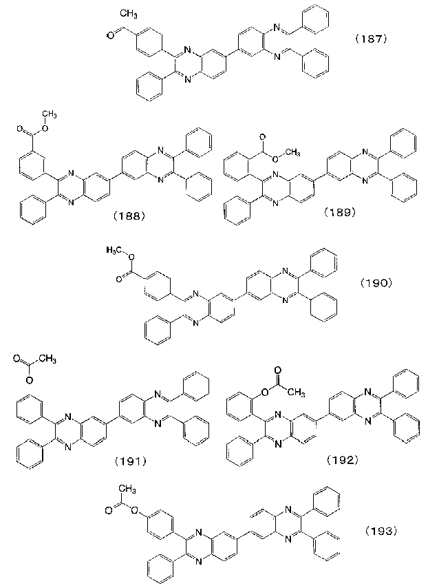
[화 21][Figure 21]

[화 22][22]

[화 23][23]
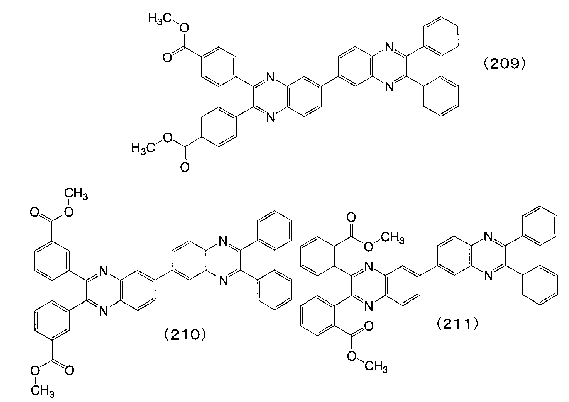
또한 전술한 것처럼, 제4 유기 화합물의 LUMO 준위는, 제5 유기 화합물의 LUMO 준위보다 0.3eV 이상 낮은 것이 바람직하다. 따라서, 사용하는 제4 유기 화합물의 종류에 따라, 그러한 조건을 만족시키도록 적절히 제5 유기 화합물을 선택하면 좋다. 예를 들면, 제4 유기 화합물로서 상기 구조식 (101)으로 나타내는 2,3,2'3'-테트라키스(4-플루오르페닐)-6,6'-비퀴녹살린(약칭:FDPQ2)이나 2,3-비스(4-플루오르페닐)퀴녹살린(약칭:FDPQ)을 사용할 경우, 제3 유기 화합물로서 Alq를 사용함으로써 상기의 조건을 만족하게 된다.As described above, the LUMO level of the fourth organic compound is preferably lower by 0.3 eV or more than the LUMO level of the fifth organic compound. Therefore, depending on the type of the fourth organic compound to be used, the fifth organic compound may be appropriately selected so as to satisfy such conditions. For example, as the fourth organic compound, 2,3,2'3'-tetrakis (4-fluorophenyl) -6,6'-nonquinoxaline (abbreviation: FDPQ2) represented by the structural formula (101) When 3-bis (4-fluorophenyl) quinoxaline (abbreviation: FDPQ) is used, the above conditions are satisfied by using Alq as the third organic compound.
도 3은, 도 1에 나타낸 녹색 발광소자의 밴드 도의 일례다. 도 3에 있어서, 양극(101G)으로부터 주입된 정공은, 정공주입층(111G), 정공수송층(112G)을 통해, 발광층(113G)에 주입된다. 한편, 음극(102G)으로부터 주입된 전자는, 전자주입층(115G), 전자수송층(114G)을 통해, 캐리어의 이동을 제어하는 층(116G)에 주입된다. 캐리어의 이동을 제어하는 층(116G)에 주입된 전자는, 전자 트랩성을 가지는 제4 유기 화합물에 의해, 전자의 이동이 느려진다. 느려진 전자는, 발광층(113G)에 주입되고, 정공과 재결합하여, 발광한다.3 is an example of a band diagram of the green light emitting element shown in Fig. 3, holes injected from the
예를 들면, 발광층(113G)이 전자수송성을 가질 경우, 정공수송층(112G)에서 발광층(113G)으로 주입된 정공은 이동이 느려진다. 또한 캐리어의 이동을 제어하는 층(116G)에서 발광층(113G)으로 주입된 전자는, 캐리어의 이동을 제어하는 층(116G)에서 이동이 느려졌기 때문에, 발광층(113G)에서도 이동이 느리다. 따라서, 이동이 느린 정공과 이동이 느린 전자가 발광층(113G)에서 재결합하기 때문에, 재결합 확률이 높아져, 발광 효율이 향상된다.For example, when the
만약, 캐리어의 이동을 제어하는 층(116)을 설치하지 않은 종래의 발광소자라면, 전자의 이동이 느려지지 않은 상태로 발광층(113G)에 주입되어, 정공수송층(112G)의 계면 부근까지 도달한다. 그 때문에 발광 영역은 정공수송층(112G)과 발광층(113G)의 계면 근방에 형성된다. 그 경우, 전자가 정공수송층(112G)에까지 도달해버려, 정공수송층(112G)을 열화시킬 우려가 있다. 또한 시간이 지남에 따라 정공수송층(112G)에까지 도달해버리는 전자의 양이 늘어나면, 시간이 지남에 따라 발광층 내에서의 재결합 확률이 저하되어 가기 때문에, 소자 수명의 저하(휘도의 시간에 따른 열화)로 이어지게 된다.If the light emitting element is not provided with the layer 116 for controlling the movement of the carrier, the electrons are injected into the
본 실시의 형태에 나타내는 녹색 발광소자에 있어서, 음극(102G)으로부터 주 입된 전자는, 전자주입층(115G), 전자수송층(114G)을 통해, 캐리어의 이동을 제어하는 층(116G)에 주입된다. 여기에서, 캐리어의 이동을 제어하는 층(116G)은, 전자수송성을 가지는 제3 유기 화합물에, 전자를 트랩하는 기능을 가지는 제4 유기 화합물을 첨가한 구성으로 되어 있다. 따라서, 캐리어의 이동을 제어하는 층(116G)에 주입된 전자는, 그 이동이 느려지고, 발광층(113G)에의 전자주입이 제어된다. 그 결과, 종래에는 정공수송성이 높은 물질이 포함되는 정공수송층(112G)과 발광층(113G)과의 계면 근방에서 형성되었을 발광 영역이, 본 실시의 형태에서 나타내는 발광소자에서는, 발광층(113)으로부터, 발광층(113)과 캐리어의 이동을 제어하는 층(116G)의 계면 부근에 걸쳐서 발광 영역(131G)이 형성되게 된다. 따라서, 전자가 정공수송층(112G)에까지 도달해버려, 정공수송성이 높은 물질이 포함되는 정공수송층(112G)을 열화시킬 가능성이 낮아진다. 또 정공에 대해서도, 캐리어의 이동을 제어하는 층(116G)이 전자수송성을 가지는 제3 유기 화합물을 가지기 때문에, 정공이 전자수송층(114G)에까지 도달해서 전자수송성이 높은 물질이 포함되는 전자수송층(114G)을 열화시킬 가능성은 작다.In the green light emitting element shown in this embodiment mode, electrons injected from the
또한, 캐리어의 이동을 제어하는 층(116G)에 있어서, 단순히 전자이동도가 느린 물질을 적용하는 것이 아니고, 전자수송성을 가지는 유기 화합물에 전자를 트랩하는 기능을 가지는 유기 화합물을 첨가하는 점이 중요하다. 즉, 단일 물질에 의해 캐리어 밸런스를 제어하는 경우에 비해, 캐리어 밸런스의 변화가 일어나기 어렵다. 예를 들면, 단일 물질로 형성된 층에서 전자의 이동을 제어하는 경우에는, 부분적으로 몰폴로지가 변화하는 것이나, 부분적으로 결정화하는 것에 의해, 층 전체 의 밸런스가 변화해버린다. 그 때문에 시간에 따른 변화에 약하다. 그러나 본 실시의 형태에서 나타낸 바와 같이, 캐리어의 이동을 제어하는 층(116G)에 포함되어 있는 성분 중 적은 성분으로 전자의 이동을 제어함으로써, 몰폴로지의 변화나 결정화, 응집 등의 영향이 작아져, 시간에 따른 변화가 일어나기 어렵다. 따라서, 시간에 따른 발광 효율의 저하가 발생하기 어려운 장수명의 발광소자를 얻을 수 있다.It is also important to add an organic compound having a function of trapping electrons to an organic compound having electron transportability, instead of simply applying a substance having a low electron mobility, in the
본 실시의 형태에 나타내는 녹색 발광소자는, 발광층과 정공수송층의 계면 또는 발광층과 전자수송층의 계면에 발광 영역이 형성되어 있지 않기 때문에, 정공수송층이나 전자수송층에 발광 영역이 근접하는 것에 의한 열화의 영향을 받지 않는다. 또한 캐리어 밸런스의 시간에 따른 변화(특히 전자주입량의 시간에 따른 변화)를 억제할 수 있다. 따라서, 열화가 적고, 수명이 긴 발광소자를 얻을 수 있다.In the green light emitting element shown in this embodiment mode, since the light emitting region is not formed at the interface between the light emitting layer and the hole transporting layer or the interface between the light emitting layer and the electron transporting layer, the influence of deterioration due to the light emitting region being close to the hole transporting layer or the electron transporting layer . It is also possible to suppress a change in carrier balance with time (in particular, a change in electron injection amount with time). Accordingly, a light emitting element having less deterioration and having a longer lifetime can be obtained.
또한, 캐리어의 이동을 제어하는 층(116G)의 막 두께는, 5nm 이상 20nm 이하인 것이 바람직하다. 막 두께가 지나치게 두꺼우면, 캐리어의 이동 속도를 지나치게 저하하게 되어, 구동전압이 높아진다. 또한 막 두께가 지나치게 얇으면, 캐리어의 이동을 제어하는 기능이 실현되지 않는다. 따라서, 5nm 이상 20nm 이하의 막 두께인 것이 바람직하다.The thickness of the
전자수송층(114G)으로서는, 전자수송층(114B)과 같은 구성을 사용할 수 있다. 전자수송층(114B)과 같은 재료를 사용해서 전자수송층(114G)을 형성해도 좋고, 다른 재료를 사용해서 전자수송층(114G)을 형성해도 좋다. 전자수송층(114B)과 같은 재료를 사용해서 전자수송층(114G)을 형성한 경우, 공정 수를 늘리지 않고 발광장치를 제조할 수 있으므로, 바람직하다.As the
전자주입층(115G)으로서는, 전자주입층(115B)과 같은 구성을 사용할 수 있다. 전자주입층(115B)과 같은 재료를 사용해서 전자주입층(115G)을 형성해도 좋고, 다른 재료를 사용해서 전자주입층(115G)을 형성해도 좋다. 전자주입층(115B)과 같은 재료를 사용해서 전자주입층(115G)을 형성한 경우, 공정 수를 늘리지 않고 발광장치를 제조할 수 있으므로, 바람직하다.As the
음극(102G)으로서는, 음극(102B)과 같은 구성을 사용할 수 있다. 음극(102B)과 같은 재료를 사용해서 음극(102G)을 형성해도 좋고, 다른 재료를 사용해서 음극(102G)을 형성해도 좋다. 음극(102B)과 같은 재료를 사용해서 음극(102G)을 형성했을 경우, 공정 수를 늘리지 않고 발광장치를 제조할 수 있으므로, 바람직하다.As the
이상에 서술한 것과 같은 발광소자는, 캐리어의 이동을 제어하는 층을 가진다. 캐리어의 이동을 제어하는 층은, 2종류 이상의 물질을 포함하기 때문에, 물질의 조합이나 혼합비, 막 두께 등을 제어함으로써, 캐리어 밸런스를 정밀하게 제어할 수 있다.The light emitting element as described above has a layer for controlling the movement of the carrier. Since the layer for controlling the movement of the carrier contains two or more kinds of materials, it is possible to precisely control the carrier balance by controlling the combination of materials, mixing ratio, film thickness, and the like.
또한 물질의 조합이나 혼합비, 막 두께 등의 제어로 캐리어 밸런스를 제어할 수 있기 때문에, 종래보다 용이하게 캐리어 밸런스의 제어가 가능해 진다. 즉, 사용하는 재료 자체의 물성을 변화시키지 않아도, 혼합비나 막 두께 등에 따라, 캐리어의 이동을 제어할 수 있다.Further, since the carrier balance can be controlled by controlling the combination of materials, the mixing ratio, the film thickness, and the like, the carrier balance can be controlled more easily than before. That is, the movement of the carrier can be controlled according to the mixing ratio, the film thickness, and the like without changing the physical properties of the material itself.
이에 따라 과잉의 전자가 주입되는 것이나, 발광층을 뚫고 나가서 정공수송층이나 정공주입층에 전자가 도달하는 것을 억제하여, 시간에 따른 발광 효율의 저하를 억제할 수 있다. 즉, 장수명의 발광소자를 얻을 수 있다.As a result, excessive electrons are injected, electrons are prevented from reaching the hole transporting layer or the hole injecting layer through the light emitting layer, and the deterioration of the luminous efficiency over time can be suppressed. That is, a long-life light emitting element can be obtained.
또한 캐리어의 이동을 제어하는 층에 포함되는 2종류 이상의 물질 중, 제3 유기 화합물보다도 적게 포함되어 있는 제4 유기 화합물을 사용해서 전자의 이동을 제어하고 있다. 따라서, 캐리어의 이동을 제어하는 층에 포함되어 있는 성분 중 적은 성분으로 전자의 이동을 제어할 수 있기 때문에, 시간에 따른 변화에 강하여, 발광소자의 장기 수명화를 실현할 수 있다. 즉, 단일 물질에 의해 캐리어 밸런스를 제어하는 경우에 비해, 캐리어 밸런스의 변화가 일어나기 어렵다. 예를 들면 단일 물질로 형성된 층에서 전자의 이동을 제어할 경우에는, 부분적으로 몰폴로지가 변화되는 것이나, 부분적으로 결정화되는 것에 의해, 층 전체의 밸런스가 변화되어버린다. 그 때문에 시간에 따른 변화에 약하다. 그러나, 본 실시의 형태에 나타낸 바와 같이 캐리어의 이동을 제어하는 층에 포함되어 있는 성분 중 적은 성분으로 전자의 이동을 제어함으로써, 몰폴로지의 변화나 결정화, 응집 등의 영향이 작아져, 시간에 따른 변화가 일어나기 어렵다. 따라서, 시간에 따른 발광 효율의 저하가 발생하기 어려운 장수명의 발광소자를 얻을 수 있다.Further, among the two or more kinds of substances contained in the layer for controlling the movement of the carrier, the movement of electrons is controlled by using a fourth organic compound which is contained less than the third organic compound. Therefore, since the movement of the electrons can be controlled with a small amount of the components contained in the layer for controlling the movement of the carrier, it is strong against the change with time, and the longevity of the light emitting element can be realized. That is, the carrier balance is unlikely to change as compared with the case where the carrier balance is controlled by a single material. For example, in the case of controlling the movement of electrons in a layer formed of a single material, the balance of the entire layer is changed by partially changing the morphology or by partially crystallizing. It is therefore vulnerable to changes over time. However, as shown in the present embodiment, by controlling the movement of electrons with fewer components among the components contained in the layer for controlling the movement of carriers, the influence of changes in the morphology, crystallization, cohesion and the like is reduced, It is difficult for the change to occur. Therefore, it is possible to obtain a long-life light-emitting element which is less liable to deteriorate in luminous efficiency with time.
<적색 발광소자>≪ Red light emitting element &
양극(101R)으로서는, 양극(101B)과 같은 구성을 사용할 수 있다. 양극(101B)과 같은 재료를 사용해서 양극(101R)을 형성해도 좋고, 다른 재료를 사용해서 양극(101R)을 형성해도 좋다. 양극(101B)과 같은 재료를 사용해서 양극(101R)을 형성한 경우, 공정 수를 늘리지 않고 발광장치를 제조할 수 있으므로, 바람직하다.As the
EL층(103R)은, 층의 적층 구조에 대해서는 특별히 한정되지 않고, 전자수송성이 높은 물질 또는 정공수송성이 높은 물질, 전자주입성이 높은 물질, 정공주 입성이 높은 물질, 바이폴라성(전자 및 정공의 수송성이 높은 물질) 물질 등을 포함한 층과, 본 실시의 형태에서 나타내는 발광층을 적절히 조합하여 구성하면 좋다. 예를 들면 정공주입층, 정공수송층, 발광층, 전자수송층, 전자주입층 등을 적절히 조합하여 구성할 수 있다. 각 층을 구성하는 재료에 대해서 이하에 구체적으로 나타낸다.The
발광층(113R)은, 발광성이 높은 물질과, 제5 유기 화합물과, 제6 유기 화합물을 포함한다.The
발광층(113R)에 있어서, 제5 유기 화합물은, 정공수송성을 가지는 화합물이다. 구체적으로는, 4,4'-비스[N-(1-나프틸)-N-페닐아미노]비페닐(약칭:NPB), 4,4'-비스[N-(9-페난트릴)-N-페닐아미노]비페닐(약칭:PPB), 4,4'-비스[N-(3-메틸페닐)-N-페닐아미노]비페닐(약칭:TPD), 4,4'-비스[N-(9,9-디메틸플루오렌-2-일)-N-페닐아미노]비페닐(약칭:DFLDPBi), 4,4',4"-트리스(N,N-디페닐아미노)트리페닐아민(약칭:TDATA), 4,4',4"-트리스[N-(3-메틸페닐)-N-페닐아미노]트리페닐아민(약칭:m-MTDATA), 4,4',4"-트리(N-카르바졸일)트리페닐아민(약칭:TCTA), 1,1-비스[4-(디페닐아미노)페닐]시클로헥산(약칭:TPAC), 9,9-비스[4-(디페닐아미노)페닐]플루오렌(약칭:TPAF), 4-(9-카르바졸일)-4'-(5-페닐-1,3,4-옥사디아졸-2-일)트리페닐아민(약칭:YGAO11), N-[4-(9-카르바졸일)페닐]-N-페닐-9,9-디메틸플루오렌-2-아민(약칭:YGAF) 등의 방향족 아민 화합물이나, 4,4'-디(N-카르바졸일)비페닐(약칭:CBP), 1,3-비스(N-카르바졸일)벤젠(약칭:mCP), 1,3,5-트리스(N-카르바졸일)벤젠(약칭:TCzB) 등의 카르바졸 유도 체를 사용할 수 있다. 방향족 아민 화합물로서는, 폴리(4-비닐트리페닐아민)(약칭:PVTPA) 등의 고분자 화합물을 사용할 수도 있다. 또한 카르바졸 유도체로서는, 폴리(N-비닐카르바졸)(약칭:PVK) 등의 고분자 화합물을 사용할 수도 있다. 이때, 전술한 제5 유기 화합물의 삼중항 여기 에너지는, 발광층(113R)에 포함되는 발광성이 높은 물질의 삼중항 여기 에너지보다도 큰 것이 바람직하다.In the
한편, 제6 유기 화합물은, 전자수송성을 가지는 화합물이다. 구체적으로는, 9-[4-(5-페닐-1,3,4-옥사디아졸-2-일)페닐]카르바졸(약칭:CO11), 1,3-비스[5-(p-tert-부틸페닐)-1,3,4-옥사디아졸-2-일]벤젠(약칭:OXD-7), 2-(4-비페닐일)-5-(4-tert-부틸페닐)-1,3,4-옥사디아졸(약칭:PBD), 2,2',2"-(1,3,5-벤젠트리일)트리스(1-페닐-1H-벤즈이미다졸)(약칭:TPBI), 3-(4-tert-부틸페닐)-4-페닐-5-(4-비페닐일)-1,2,4-트리아졸(약칭:TAZ), 3-(4-tert-부틸페닐)-4-(4-에틸페닐)-5-(4-비페닐일)-1,2,4-트리아졸(약칭:p-EtTAZ), 9,9',9"-[1,3,5-트리아진-2,4,6-트리일]트리카르바졸(약칭:TCzTRZ), 2,2',2"-(1,3,5-벤젠트리일)트리스(6,7-디메틸-3-페닐퀴녹살린)(약칭:TriMeQn), 9,9'-(퀴녹살린-2,3-디일디-4,1-페닐렌)디(9H-카르바졸)(약칭:CzQn), 3,3',6,6'-테트라페닐-9,9'-(퀴녹살린-2,3-디일디-4,1-페닐렌)디(9H-카르바졸)(약칭:DCzPQ), 바소페난트롤린(약칭:BPhen), 바소큐프로인(약칭:BCP) 등의 복소 방향족 화합물이나, 비스(2-메틸-8-퀴놀리노라토)(4-페닐페놀라토)알루미늄(III)(약칭:BAlq), 트리스[2-(2-히드록시페닐)-5-페닐-1,3,4-옥사디아졸라토]알루미늄(III)(약칭:A l(OXD)3), 트리스(2-히드록시페닐-1-페닐-1H-벤즈이미다졸라토)알루미늄(III)(약칭:Al(BIZ)3), 비스[2-(2-히드록시페닐)벤조티아졸라토]아연(II)(약칭:Zn(BTZ)2), 비스[2-(2-히드록시페닐)벤즈옥사졸라토]아연(II)(약칭:Zn(PBO)2) 등의 금속착체를 사용할 수 있다. 복소 방향족 화합물로서는, 폴리(2,5-피리딘-디일)(약칭:PPy)과 같은 고분자 화합물을 사용할 수도 있다. 또한 금속착체로서는, 하기 참고 문헌에 개시되어 있는 바와 같은 금속착체 고분자 화합물을 사용할 수도 있다(참고 문헌; X.T. Tao, 외 5명, 어플라이드 피직스 레터즈, Vol.70(12), 1503-1505(1997)). 이때, 전술한 제6 유기 화합물의 삼중항 여기 에너지는, 피라진계 유기 금속착체의 삼중항 여기 에너지보다도 큰 것이 바람직하다.On the other hand, the sixth organic compound is a compound having an electron transporting property. Specific examples thereof include 9- [4- (5-phenyl-1,3,4-oxadiazol-2-yl) phenyl] carbazole (abbreviated as CO11), 1,3- (4-biphenyl) -1,3,4-oxadiazol-2-yl] benzene (abbreviation: OXD-7) (Abbreviation: PBD), 2,2 ', 2 "- (1,3,5-benzenetriyl) tris (1-phenyl-1H-benzimidazole) (4-tert-butylphenyl) -4-phenyl-5- (4-biphenylyl) -1,2,4- triazole (TAZ) (Abbrev.: P-EtTAZ), 9,9 ', 9 "- [1,3,5 -Triazine-2,4,6-triyl] tricarbazole (abbreviated as TCzTRZ), 2,2 ', 2 "- (1,3,5-benzenetriyl) tris (6,7- - (phenylquinoxaline) (abbreviation: TriMeQn), 9,9 '- (quinoxaline-2,3-diyldi-4,1-phenylene) di (9H-carbazole) (abbreviation: CzQn) ', 6,6'-tetraphenyl-9,9' - (quinoxaline-2,3-diyldi-4,1-phenylene) di (9H- carbazole) (abbreviation: DCzPQ), basophenanthroline ( (2-methyl-8-quinolinolato) (4-phenylphenolato) aluminum (III) (abbreviation: BAlq) (III) (abbreviation: Al (OXD) 3 ), tris (2-hydroxyphenyl) -5-phenyl-1,3,4-oxadiazolato] (Abbreviation: Al (BIZ) 3 ), bis [2- (2-hydroxyphenyl) benzothiazolato] zinc (II) Metal complexes such as Zn (BTZ) 2 and bis [2- (2-hydroxyphenyl) benzoxazolato] zinc (II) (abbreviation: Zn (PBO) 2 ) A polymer compound such as poly (2,5-pyridine-diyl) (abbreviation: PPy) may be used. As metal complexes, metal complex polymer compounds as disclosed in the following references can also be used XT Tao, 5 others, Applied Physics Letters Queens, Vol.70 (12), 1503-1505 (1997)). At this time, it is preferable that the triplet excitation energy of the sixth organic compound is larger than the triplet excitation energy of the pyrazine organic metal complex.
발광층(113R)에 포함되는 발광성이 높은 물질로서는, 인광을 발광하는 물질을 사용할 수 있다. 예를 들면, 비스[2-(2'-벤조[4,5-α]티에닐)피리디나토-N,C3']이리듐(아세틸아세토나토)(약칭:Ir(btp)2(acac)), 비스(1-페닐이소퀴놀리나토-N,C2')이리듐(III)아세틸아세토나토(약칭:Ir(piq)2(acac)), 트리스(1-페닐이소퀴놀리나토-N,C2')이리듐(III)(약칭:Ir(piq)3) 등을 들 수 있다. 특히, 배위자가 피라진 골격을 가지고, 중심금속이 제9족 또는 제10족인 유기 금속착체(이하, 「피라진계 유기 금속착체」라고 한다)가, 지금까지 보고되어 온 인광성의 유기 금속착체에 비해, 상당히 고효율로 인광을 발한다는 점에서 바람직하다.As the substance having high luminescence contained in the
도 4는, 도 1에 나타낸 적색 발광소자의 밴드 도의 일례다. 도 4에 있어서의 발광층(113R)은, 정공수송성의 제5 유기 화합물과, 전자수송성의 제6 유기 화합물과, 피라진계 유기 금속착체를 포함하고 있다. 상기 피라진계 유기 금속착체의 LUMO 준위(232)는, 제5 유기 화합물의 LUMO 준위(212) 및 제6 유기 화합물의 LUMO 준위(222)보다도 낮기 때문에, 전자는 피라진계 유기 금속착체의 LUMO 준위(232)로 트랩 된다. 다만, 제6 유기 화합물은 전자수송성이기 때문에, 전자는 피라진계 유기 금속착체의 LUMO 준위(232)로 트랩 되면서도, 조금씩 정공수송층(112R) 측으로 이동할 수 있다. 한편, 제5 유기 화합물이 정공수송성이며, 또 정공을 받아들이기 쉬운 성질도 있기 때문에, 정공은 우선 제5 유기 화합물의 HOMO 준위(211)로 주입된다. 제6 유기 화합물의 HOMO 준위(221)로는 주입되기 어렵다. 이때, 제5 유기 화합물의 양을 조절함으로써, 주입된 정공의 이동 속도를 조절할 수 있기 때문에, 전자수송층(114R) 측으로부터 오는 전자의 이동 속도와 맞출 수 있다. 즉, 발광층(113R) 내에서, 정공과 전자의 밸런스를 잘 취할 수 있는 것이다. 그리고, 정공은 피라진계 유기 금속착체의 HOMO 준위(231)로 주입되고, 트랩 되어 있는 전자와 재결합해서 발광을 얻을 수 있다. 이러한 구성의 발광소자에 있어서, 발광층(113R)에 포함되는 제5 유기 화합물, 제6 유기 화합물, 피라진계 유기 금속착체의 양을 조정함으로써, 발광 영역(131R)의 위치를 조정할 수 있다.Fig. 4 is an example of a band diagram of the red light emitting element shown in Fig. The
이상에 서술한 바와 같은 제5 유기 화합물, 제6 유기 화합물, 및 피라진계 유기 금속착체를 적절히 조합함으로써, 발광층은 구성된다. 이때, 피라진계 유기 금속착체의 구체적인 예에 대해서는, 실시의 형태 2에 상세히 설명한다. 다만, 발광층은 다른 물질을 더 함유해도 된다.By appropriately combining the fifth organic compound, the sixth organic compound, and the pyrazine organic metal complex as described above, the light emitting layer is constituted. Specific examples of the pyrazine-based organometallic complexes will be described in detail in the second embodiment. However, the light emitting layer may further contain another substance.
여기에서, 상기 발광층에 있어서, 적어도 제5 유기 화합물과 제6 유기 화합물 중 어느 한쪽이 호스트 재료가 되고, 피라진계 유기 금속착체가 게스트 재료가 되는 구성이 바람직하다. 이는 피라진계 유기 금속착체의 농도 소광을 방지하기 위해서다. 또한 발광층에 있어서의 캐리어 밸런스를, 제5 유기 화합물과 제6 유기 화합물로 조절하기 위해서다.It is preferable that at least one of the fifth organic compound and the sixth organic compound be a host material and the pyrazine organic metal complex be a guest material in the light emitting layer. This is to prevent concentration quenching of the pyrazine-based organometallic complex. And the carrier balance in the light emitting layer is controlled by the fifth organic compound and the sixth organic compound.
따라서, 본 실시의 형태의 발광소자에 있어서는, 제5 유기 화합물 및/또는 제6 유기 화합물의 양은, 피라진계 유기 금속착체보다도 많은 것이 바람직하다. 구체적으로는, 체적분률 또는 질량분률이 많은 것이 바람직하다. 또한 농도 소광방지의 관점에서는, 피라진계 유기 금속착체의 발광층에 있어서의 비율이, 1질량% 이상 10질량% 이하인 것이 바람직하다.Therefore, in the light emitting device of the present embodiment, the amount of the fifth organic compound and / or the sixth organic compound is preferably larger than that of the pyrazine organic metal complex. Specifically, it is preferable that the volume fraction or the mass fraction is large. From the viewpoint of preventing concentration and extinction, it is preferable that the proportion of the pyrazine-based organometallic complex in the light emitting layer is 1% by mass or more and 10% by mass or less.
또한 발광층에 있어서, 제5 유기 화합물과 제6 유기 화합물의 질량비는, 제5 유기 화합물:제6 유기 화합물=1:20∼20:1의 범위가 바람직하다. 즉, 제5 유기 화합물에 대한 제6 유기 화합물의 질량비가, 1/20 이상 20 이하로 되는 것이 바람직하다. 이 범위 밖인 경우, 제5 유기 화합물과 피라진계 유기 금속착체만이 포함되어 있는 상태, 또는, 제6 유기 화합물과 피라진계 유기 금속착체만이 포함되어 있는 상태와 실질적으로 같아질 가능성이 있기 때문이다.In the light emitting layer, the mass ratio of the fifth organic compound and the sixth organic compound is preferably in the range of the fifth organic compound: the sixth organic compound = 1: 20 to 20: 1. That is, the mass ratio of the sixth organic compound to the fifth organic compound is preferably 1/20 or more and 20 or less. If it is outside this range, there is a possibility that only the fifth organic compound and the pyrazine organic metal complex are included, or the state containing only the sixth organic compound and the pyrazine organic metal complex is substantially the same .
또한 본 발명자들은 발광층에 있어서, 정공수송성의 제5 유기 화합물과 비교 하여, 전자수송성의 제6 유기 화합물이 같은 양 존재하거나, 많은 구성이, 특히 효과적이라는 것을 알아냈다. 이는 일반적인 유기 화합물에 있어서, 정공이동도가 전자이동도보다도 높은 것에 기인한다고 여겨진다. 따라서 본 발명에서는, 제5 유기 화합물에 대한 제6 유기 화합물의 질량비가, 1 이상 20 이하인 것이 더욱 바람직하다. 특히 수명에 대한 효과가 현저한 것은, 5 이상 20 이하다.Further, the inventors of the present invention have found that, in the light-emitting layer, the sixth organic compound of the electron transporting property is present in the same amount or a large number of compositions are particularly effective as compared with the fifth organic compound of the hole transporting property. It is considered that this is due to the fact that, in a general organic compound, the hole mobility is higher than the electron mobility. Therefore, in the present invention, the mass ratio of the sixth organic compound to the fifth organic compound is more preferably 1 or more and 20 or less. Particularly, the effect on the service life is not less than 5 and not more than 20.
이때, 본 발명에서 사용하는 피라진계 유기 금속착체의 전자 트랩성은, 구체적으로는, 제5 유기 화합물의 LUMO 준위 및 제6 유기 화합물의 LUMO 준위와 비교하여, 0.2eV 이상 깊은 경우가 많다. 그리고, 그러한 경우에 수명 개선 효과 및 효율 개선 효과가 현저하기 때문에, 제5 유기 화합물의 LUMO 준위 및 제6 유기 화합물의 LUMO 준위에 비해, 피라진계 유기 금속착체의 LUMO 준위가 0.2eV 이상 깊은 것도 특징이다.At this time, the electron trapping property of the pyrazine-based organometallic complex used in the present invention is more deeply deeper than 0.2 eV in comparison with the LUMO level of the fifth organic compound and the LUMO level of the sixth organic compound. In this case, the LUMO level of the pyrazine-based organometallic complex is at least 0.2 eV in deeper than the LUMO level of the fifth organic compound and the LUMO level of the sixth organic compound, to be.
다음에 발광층(113R) 이외의 층에 관하여 설명한다. 정공수송층(112R) 및 정공주입층(111R)은, 반드시 필요한 것은 아니고, 적절히 설치하면 된다. 이들 층을 구성하는 구체적인 재료로서는, 정공수송성 화합물이 바람직하고, 전술한 NPB, PPB, TPD, DFLDPBi, TDATA, m-MTDATA, TCTA, TPAC, TPAF, YGAO11, YGAF, CBP, mCP, TCzB, PVTPA, PVK 등을 사용할 수 있다. 또한 9,10-비스[4-(디페닐아미노)페닐]안트라센(약칭:TPA2A), 2-tert-부틸-9,10-디(2-나프틸)안트라센(약칭:t-BuDNA)과 같이, 삼중항 여기 에너지가 낮은 안트라센 유도체도 사용할 수 있다.Next, the layers other than the light-emitting
이 특징은, 아래와 같이 설명할 수 있다. 발광층(113R)은, 상기한 바와 같이 캐리어 밸런스가 좋기 때문에, 발광 영역이 발광층(113R)과 정공수송층(112R)의 계면에 치우치지 않는다. 따라서, 정공수송층(112R)에, 피라진계 유기 금속착체(223)보다도 삼중항 여기 에너지가 낮은 물질을 적용하더라도, 그것이 피라진계 유기 금속착체(223)에 대한 소광제(quencher)가 되기 어렵기 때문이다.This feature can be described as follows. Since the
요컨대, 삼중항 여기 에너지를 고려할 필요가 없기 때문에, 사용하는 재료의 선택 사항이 넓혀진다. 따라서, 정공수송층(112R)으로서는, 정공수송층(112B)과 같은 구성을 사용할 수 있다. 정공수송층(112B)과 같은 재료를 사용해서 정공수송층(112R)을 형성해도 좋고, 다른 재료를 사용해서 정공수송층(112R)을 형성해도 좋지만, 정공수송층(112B)과 같은 재료를 사용해서 정공수송층(112R)을 형성한 경우, 공정 수를 늘리지 않고 발광장치를 제조할 수 있으므로, 바람직하다.In short, since there is no need to consider the triplet excitation energy, the choice of materials to be used is expanded. Therefore, the same structure as that of the
마찬가지로, 정공주입층(111R)으로서는, 정공주입층(111B)과 같은 구성을 사용할 수 있다. 정공주입층(111B)과 같은 재료를 사용해서 정공주입층(111R)을 형성해도 좋고, 다른 재료를 사용해서 정공주입층(111R)을 형성해도 좋지만, 정공주입층(111B)과 같은 재료를 사용해서 정공주입층(111R)을 형성한 경우, 공정 수를 늘리지 않고 발광장치를 제조할 수 있으므로, 바람직하다.Similarly, as the
전자수송층(114R) 및 전자주입층(115R)은, 반드시 필요한 것은 아니고, 적절히 설치하면 된다. 이들 층을 구성하는 구체적인 재료로서는, 전자수송성 화합물이 바람직하고, 전술한 CO11, OXD-7, PBD, TPBI, TAZ, p-EtTAZ, TCzTRZ, TriMeQn, CzQn, DCzPQ, BPhen, BCP, BA lq, Al(OXD)3, Al(BIZ)3, Zn(BTZ)2, Zn(PBO)2, PPy 등을 사용할 수 있다. 또한 트리스(8-퀴놀리노라토)알루미늄(III)(약칭:Alq), 트리스(4-메틸-8-퀴놀리노라토)알루미늄(III)(약칭:Almq3), 비스(10-히드록시벤조[h]퀴놀리나토)베릴륨(II)(약칭:BeBq2)과 같이, 삼중항 여기 에너지가 낮은 물질도 사용할 수 있다(예를 들면 Alq의 인광 스펙트럼은, 심적색의 650∼700nm 정도라는 것이 보고되어 있다).The electron-transporting
이 특징은, 아래와 같이 설명할 수 있다. 발광층(113R)은, 상기한 바와 같이 캐리어 밸런스가 좋기 때문에, 발광 영역이 발광층(113R)와 전자수송층(114R)의 계면에 치우치지 않는다. 따라서, 전자수송층(114R)에, 피라진계 유기 금속착체(223)보다도 삼중항 여기 에너지가 낮은 물질을 적용하더라도, 그것이 피라진계 유기 금속착체(223)에 대한 소광제(quencher)가 되기 어렵기 때문이다.This feature can be described as follows. Since the
요컨대, 삼중항 여기 에너지를 고려할 필요가 없기 때문에, 사용하는 재료의 선택 사항이 넓혀진다. 따라서, 전자수송층(114R)으로서는, 전자수송층(114B)과 같은 구성을 사용할 수 있다. 전자수송층(114B)과 같은 재료를 사용해서 전자수송층(114R)을 형성해도 좋고, 다른 재료를 사용해서 전자수송층(114R)을 형성해도 좋지만, 전자수송층(114B)과 같은 재료를 사용해서 전자수송층(114R)을 형성한 경우, 공정 수를 늘리지 않고 발광장치를 제조할 수 있으므로, 바람직하다.In short, since there is no need to consider the triplet excitation energy, the choice of materials to be used is expanded. Therefore, as the
마찬가지로, 전자주입층(115R)으로서는, 전자주입층(115B)과 같은 구성을 사용할 수 있다. 전자주입층(115B)과 같은 재료를 사용해서 전자주입층(115R)을 형성 해도 좋고, 다른 재료를 사용해서 전자주입층(115R)을 형성해도 좋지만, 전자주입층(115B)과 같은 재료를 사용해서 전자주입층(115R)을 형성한 경우, 공정 수를 늘리지 않고 발광장치를 제조할 수 있으므로, 바람직하다.Similarly, as the
음극(102R)으로서는, 음극(102B)과 같은 구성을 사용할 수 있다. 음극(102B)과 같은 재료를 사용해서 음극(102R)을 형성해도 좋고, 다른 재료를 사용해서 음극(102R)을 형성해도 좋다. 음극(102B)과 같은 재료를 사용해서 음극(102R)을 형성했을 경우, 공정 수를 늘리지 않고 발광장치를 제조할 수 있으므로, 바람직하다.As the
이렇게, 청색 발광소자, 녹색 발광소자, 적색 발광소자를 각각 최적의 구성으로 함으로써 특성이 우수한 본 발명의 발광장치를 얻을 수 있다.In this manner, the blue light emitting element, the green light emitting element, and the red light emitting element can be optimally configured, respectively, and the light emitting device of the present invention having excellent characteristics can be obtained.
또한 본 발명의 발광장치에 있어서, 각 발광소자의 발광층 이외의 층을 공통으로 제조할 수 있다. 즉, 발광층 이외의 층의 구성을 동일 구성으로 할 수 있다. 도 12에는, 발광층 이외의 층을 공통으로 제조한 발광장치의 일례를 게시한다. 우선, 각 발광소자에 공통으로, 기판(1100) 위에, 양극(1101), 정공주입층(1111), 정공수송층(1112)을 형성한다. 그 후에 발광색마다, 발광층(1113B), 발광층(1113G) 및 캐리어의 이동을 제어하는 층(1116G), 발광층(1113R)을 형성한다. 그리고, 다시, 각 발광소자에 공통으로, 전자수송층(1114), 전자주입층(1115), 음극(1102)을 형성한다. 도 12에 나타낸 바와 같이, 발광층 이외의 층의 구성을 동일 구성으로 함으로써, 발광장치의 제조 공정의 간략화가 가능해 진다.In the light emitting device of the present invention, layers other than the light emitting layer of each light emitting element can be commonly manufactured. That is, the layers other than the light emitting layer can have the same configuration. 12 shows an example of a light emitting device in which layers other than the light emitting layer are commonly manufactured. First, an
또한 본 발명의 발광장치에 있어서, 발광층에 있어서의 발광 영역이 각 발광소자에 따라 다르다. 구체적으로는, 청색 발광소자, 녹색 발광소자, 적색 발광소자 의 순으로, 양극으로서 기능하는 전극에 가까워지도록 할 수 있다. 상기한 바와 같이, 청색 발광소자에서는, 제1 발광층(1121B)과 제2 발광층(1122B)의 계면 부근이 발광 영역(1131B)이 된다. 또한 녹색 발광소자에서는, 발광층(1113G)으로부터, 발광층(1113G)과 캐리어의 이동을 제어하는 층(1116G)의 계면 부근에 걸쳐서 발광 영역(1131G)이 형성되게 된다. 또한 적색 발광소자에서는, 발광층(1113R)에 포함되는 제5 유기 화합물, 제6 유기 화합물, 피라진계 유기 금속착체의 양을 조정함으로써, 발광 영역(1131R)의 위치를 조정할 수 있다. 따라서, 음극을 반사 전극으로 했을 경우, 발광 파장이 짧은 청색 발광소자의 발광 영역이 음극측이 되고, 발광 파장이 길어짐에 따라, 녹색 발광소자, 적색 발광소자의 순으로 음극으로부터 멀어지도록 설계할 수 있다. 즉, 발광소자의 광학 설계에 알맞은 구성으로 되어 있다. 따라서, 반사 전극까지의 거리를 발광 파장에 최적인 광학거리로 할 수 있게 되고, 광 추출 효율을 향상시킬 수 있다.Further, in the light emitting device of the present invention, the light emitting region in the light emitting layer differs depending on each light emitting element. Specifically, the blue light emitting element, the green light emitting element, and the red light emitting element can be made to approach the electrode functioning as the anode in that order. As described above, in the blue light emitting element, the vicinity of the interface between the first
또한 EL층의 형성 방법으로서는, 건식법, 습식법을 불문하고, 여러 가지 방법을 사용할 수 있다. 예를 들면 진공증착법, 잉크젯법 또는 스핀 코트법 등을 사용해도 상관없다. 또 각 전극 또는 각 층마다 다른 성막 방법을 사용해서 형성해도 상관없다.As the method of forming the EL layer, various methods can be used regardless of the dry method and the wet method. For example, a vacuum deposition method, an inkjet method, a spin coating method, or the like may be used. It may also be formed by using different film forming methods for each electrode or each layer.
예를 들면 전술한 재료 중, 고분자 화합물을 사용해서 습식법으로 EL층을 형성해도 좋다. 또는, 저분자의 유기 화합물을 사용해서 습식법으로 형성할 수도 있다. 또한 저분자의 유기 화합물을 사용해서 진공증착법 등의 건식법을 사용해서 EL층을 형성해도 좋다.For example, among the above-mentioned materials, the EL layer may be formed by a wet process using a polymer compound. Alternatively, it may be formed by a wet process using a low-molecular organic compound. Further, an EL layer may be formed using a low-molecular organic compound by a dry method such as a vacuum evaporation method.
또한 전극에 대해서도, 졸-겔법을 사용해서 습식법으로 형성해도 좋고, 금속 재료의 페이스트를 사용해서 습식법으로 형성해도 좋다. 또한 스퍼터링법이나 진공증착법 등의 건식법을 사용해서 형성해도 좋다.The electrode may also be formed by a wet process using a sol-gel method or by a wet process using a paste of a metal material. It may also be formed by a dry method such as a sputtering method or a vacuum evaporation method.
본 실시의 형태에 나타낸 발광소자를 표시장치에 적용하여, 발광층을 나누어 도포하는 경우에는, 발광층은 습식법에 의해 형성하는 것이 바람직하다. 발광층을 잉크젯법을 사용해서 형성함으로써, 대형기판이어도 발광층을 쉽게 나누어서 도포할 수 있다.When the light-emitting element shown in this embodiment mode is applied to a display device and the light-emitting layer is applied separately, it is preferable that the light-emitting layer is formed by a wet method. By forming the light emitting layer by using the ink jet method, the light emitting layer can be easily divided even for a large substrate.
이상과 같은 구성을 가지는 본 실시의 형태에서 나타낸 발광소자는, 양극(101)과 음극(102)의 사이에 전압을 가함으로써 전류가 흐른다. 그리고, 발광성이 높은 물질을 포함한 층인 발광층(113)에서 정공과 전자가 재결합하여, 발광하는 것이다. 즉 발광층(113)에 발광 영역이 형성되도록 하는 구성으로 되어 있다.In the light emitting device shown in this embodiment having the above-described configuration, a current flows by applying a voltage between the anode 101 and the cathode 102. [ Then, holes and electrons are recombined in the light emitting layer 113, which is a layer containing a substance having a high light emitting property, to emit light. That is, a light emitting region is formed in the light emitting layer 113.
발광은 양극(101) 또는 음극(102) 중 어느 한쪽 또는 양쪽을 통해 외부로 추출된다. 따라서, 양극(101) 또는 음극(102) 중 어느 한쪽 또는 양쪽은, 투광성을 가지는 물질로 이루어진다. 양극(101)만이 투광성을 가지는 전극인 경우, 빛은 양극(101)을 통해 기판측으로부터 추출된다. 또한 음극(102)만이 투광성을 가지는 전극인 경우, 빛은 음극(102)을 통해 기판과 반대측으로부터 추출된다. 양극(101) 및 음극(102)이 모두 투광성을 가지는 전극인 경우, 빛은 양극(101) 및 음극(102)을 통해, 기판측 및 기판측과 반대측 모두로부터 추출된다.The light emission is extracted to the outside through either or both of the anode 101 and the cathode 102. Therefore, either or both of the anode 101 and the cathode 102 is made of a light-transmitting material. When only the anode 101 is an electrode having translucency, light is extracted from the substrate side through the anode 101. [ When only the cathode 102 is an electrode having transparency, light is extracted from the opposite side of the substrate through the cathode 102. [ When both the anode 101 and the cathode 102 are light-transmitting electrodes, light is extracted from both the substrate side and the opposite side of the substrate side via the anode 101 and the cathode 102.
이때, 도 1에서는, 양극(101)을 기판(100)측에 설치한 구성에 대해서 나타냈지만, 음극(102)을 기판(100)측에 형성해도 된다. 도 5에서는, 기판(100) 위에, 음 극(102), EL층(103), 양극(101)이 순차적으로 적층된 구성으로 되어 있다. EL층(103)은, 도 1에 나타내는 구성과는 역순으로 적층 되어 있다.1 shows the structure in which the anode 101 is provided on the
이때, 본 실시의 형태에서는, 유리, 플라스틱 등으로 이루어지는 기판 위에 발광소자를 제조하고 있다. 하나의 기판 위에 이러한 발광소자를 복수 제조함으로써 패시브 매트릭스형 발광장치를 제조할 수 있다. 또한 유리, 플라스틱 등으로 이루어지는 기판 위에, 예를 들면 박막 트랜지스터(TFT)를 형성하고, TFT와 전기적으로 접속된 전극 위에 발광소자를 제조해도 좋다. 이에 따라 TFT에 의해 발광소자의 구동을 제어하는 액티브 매트릭스형 발광장치를 제조할 수 있다. 이때, TFT의 구조는, 특별히 한정되지 않는다. 스태거형 TFT도 좋고, 역스태거형 TFT도 좋다. 또한 TFT기판에 형성되는 구동용 회로도, N형 및 P형 TFT로 이루어진 것도 좋고, 혹은 N형 TFT 또는 P형 TFT 중 어느 하나만으로 이루어진 것도 좋다. 또한 TFT에 사용되는 반도체막의 결정성도 특별히 한정되지 않는다. 비정질 반도체막을 사용해도 되고, 결정성 반도체막을 사용해도 된다.At this time, in this embodiment, a light emitting device is manufactured on a substrate made of glass, plastic, or the like. A passive matrix type light emitting device can be manufactured by manufacturing a plurality of such light emitting elements on one substrate. A thin film transistor (TFT), for example, may be formed on a substrate made of glass, plastic, or the like, and the light emitting element may be fabricated on an electrode electrically connected to the TFT. Thus, an active matrix type light emitting device that controls the driving of the light emitting element by the TFT can be manufactured. At this time, the structure of the TFT is not particularly limited. Stagger type TFTs may be used, and reverse stagger type TFTs may be used. Also, the driving circuit formed on the TFT substrate may be composed of N-type and P-type TFTs, or may be composed of only one of N-type TFTs or P-type TFTs. The crystallinity of the semiconductor film used for the TFT is also not particularly limited. An amorphous semiconductor film may be used, or a crystalline semiconductor film may be used.
(실시의 형태 2)(Embodiment 2)
본 실시의 형태에서는, 본 발명의 발광장치에 사용할 수 있는 피라진계 유기 금속착체의 구조에 대해서, 구체적으로 예시한다.In the present embodiment, the structure of the pyrazine-based organometallic complex which can be used in the light-emitting device of the present invention is specifically exemplified.
피라진계 유기 금속착체는 그 배위자가 피라진 골격을 가지는 배위자이며, 또 중심금속이 제9족(Co, Rh, Ir) 또는 제10족(Ni, Pd, Pt) 원소인 유기 금속착체다. 또한 상기 유기 금속착체는, 인광을 발광할 수 있는 성질을 가지면 좋다.The pyrazine-based organometallic complex is an organometallic complex in which the ligand is a ligand having a pyrazine skeleton and the central metal is a Group 9 element (Co, Rh, Ir) or a
제9족이나 제10족의 유기 금속착체는, MLCT(Metal to Ligand Charge Transfer) 천이를 나타내는 것이 많다. 특히, 인광성 화합물에 있어서는, 삼중항 MLCT 천이가 잘 관찰된다. 여기에서, MLCT 천이를 나타내는 유기 금속착체의 LUMO 준위는, 배위자의 LUMO 준위의 서열로 결정되기 때문에, LUMO 준위가 높은 배위자를 사용하면 상기 유기 금속착체의 LUMO 준위도 높아지고, LUMO 준위가 낮은 배위자를 사용하면 상기 유기 금속착체의 LUMO 준위도 낮아진다. 그리고, 피라진은 피리딘에 비해, LUMO 준위가 낮기 때문에, 본 발명에서 사용하는 피라진계 유기 금속착체는 종래의 피리딘계 유기 금속착체에 비해, LUMO 준위가 낮은(요컨대 전자 트랩성이 높은) 성질을 나타낸다.Organometallic complexes of the ninth or tenth group often exhibit a metal to ligand charge transfer (MLCT) transition. Particularly, in phosphorescent compounds, triplet MLCT transitions are well observed. Here, since the LUMO level of the organometallic complex showing the MLCT transition is determined by the sequence of the LUMO level of the ligand, if the ligand having a high LUMO level is used, the LUMO level of the organometallic complex becomes high and the ligand having a low LUMO level If used, the LUMO level of the organometallic complex is also lowered. Since the pyrazine has a lower LUMO level than pyridine, the pyrazine-based organometallic complex used in the present invention exhibits a lower LUMO level (that is, a higher electron trapping property) than the conventional pyridine-based organometallic complex .
본 발명에 사용하는 피라진계 유기 금속착체의 배위자는, 피라진 골격을 가지면 되는데, 그 중에서도, 상기 배위자가 2-아릴피라진 유도체인 경우, 그 배위자는 중심금속에 대하여 시클로 메탈화 할 수 있다. 그리고 시클로 메탈화착물은, 높은 인광 양자 수율이 가능하다. 따라서 상기 배위자는, 2-아릴피라진 유도체인 것이 바람직하다. 또한, 2-아릴피라진 유도체의 일종인 2-페닐피라진 유도체가 배위자인 경우, 그 배위자는 중심금속에 대하여 오르토 메탈화 할 수 있다.(오르토 메탈화는, 시클로 메탈화의 일종이다). 그리고 이렇게, 2-페닐피라진이 오르토 금속화한 오르토 금속착물은, 특히 높은 인광 양자 수율을 달성할 수 있다는 것을 본 발명자들은 알아냈다. 따라서, 배위자의 보다 바람직한 형태는, 2-페닐피라진 유도체다.The ligand of the pyrazine-based organometallic complex used in the present invention has a pyrazine skeleton. Among them, when the ligand is a 2-arylpyrazine derivative, the ligand can be cyclometalated with respect to the central metal. And cyclometallated complexes are capable of high phosphorescence quantum yield. Therefore, the ligand is preferably a 2-arylpyrazine derivative. When the 2-phenylpyrazine derivative as a kind of 2-arylpyrazine derivative is a ligand, the ligand can be ortho-metallized with respect to the central metal. (Orthometallation is a kind of cyclometalation). Thus, the present inventors have found that an ortho-metal complex obtained by orthometallating 2-phenylpyrazine can attain a particularly high phosphorescence quantum yield. Thus, a more preferred form of the ligand is a 2-phenylpyrazine derivative.
이하에, 2-아릴피라진 유도체를 배위자로 하는 유기 금속착체의 구체적인 예 를 열거한다.Specific examples of the organometallic complex having a 2-arylpyrazine derivative as a ligand are listed below.
[화 24][24]

[화 25][25]

여기에서, 2-페닐피라진 유도체가 오르토 금속화한 유기 금속착체 중에서도, 2,5-디페닐피라진 유도체가 오르토 금속화한 유기 금속착체는, LUMO 준위가 한층 더 깊어진다. 또한 색도가 좋은 적색 발광을 얻을 수 있다. 따라서, 배위자가 2,5-디페닐피라진 유도체인 경우, 실시의 형태 1에 나타낸 발광소자의 효과는 현저해지므로 바람직하다.Among the organometallic complexes in which the 2-phenylpyrazine derivatives are orthometallized, the organometallic complexes in which the 2,5-diphenylpyrazine derivatives are ortho metallized have a deeper LUMO level. Further, red light emission with good chromaticity can be obtained. Therefore, when the ligand is a 2,5-diphenylpyrazine derivative, the effect of the light emitting device shown in
또한 2,5-디페닐피라진 유도체가 오르토 금속화한 유기 금속착체로서는, 하기 일반식 (G1)로 나타내는 구조를 가지는 유기 금속착체를 들 수 있다.Examples of the organometallic complex in which the 2,5-diphenylpyrazine derivative is orthometallized include organometallic complexes having a structure represented by the following general formula (G1).
[화 26][26]

(식에서, R1은 알킬기, 또는 페닐기 중 어느 하나를 나타낸다. R1이 페닐기인 경우, 치환기를 더 가져도 되고, 치환기로서는, 알킬기, 할로겐, 할로 알킬기, 알콕시기, 알콕시 카르보닐기를 들 수 있다. 또한 R3은 수소, 또는 알킬기 중 어느 하나를 나타낸다. 또한 R4∼R12는 수소, 또는 알킬기, 또는 할로겐기, 또는 할로 알킬기, 또는 알콕시기, 또는 알콕시 카르보닐기 중 어느 하나를 나타낸다. 또한 M은 중심금속이며, 제9족 원소, 또는 제10족 원소 중 어느 하나를 나타낸다.)When R1 is a phenyl group, it may further have a substituent, and examples of the substituent include an alkyl group, a halogen, a haloalkyl group, an alkoxy group, and an alkoxycarbonyl group, and R < 3 >
이때, 전술한 일반식 (G1)로 나타내는 구조를 가지는 유기 금속착체는, 구체적으로는, 하기 일반식 (G2)로 나타내는 것과 같은, 피라진 유도체 이외의 배위자 L도 가지는 혼합 배위자형 유기 금속착체인 것이 바람직하다. 이것은, 합성상 용이하기 때문이다.The organometallic complex having the structure represented by the general formula (G1) described above is specifically a mixed ligand-type organometallic complex having a ligand L other than the pyrazine derivative represented by the following general formula (G2) desirable. This is because it is easy to synthesize.
[화 27][Figure 27]

(식에서, R1은 알킬기, 또는 페닐기 중 어느 하나를 나타낸다. R1이 페닐기인 경우, 치환기를 더 가져도 되고, 치환기로서는, 알킬기, 할로겐, 할로 알킬기, 알콕시기, 알콕시 카르보닐기를 들 수 있다. 또한 R3은 수소, 또는 알킬기 중 어느 하나를 나타낸다. 또한 R4∼R12는 수소, 또는 알킬기, 또는 할로겐기, 또는 할로 알킬기, 또는 알콕시기, 또는 알콕시 카르보닐기 중 어느 하나를 나타낸다. 또한 M은 중심금속이며, 제9족 원소, 또는 제10족 원소 중 어느 하나를 나타낸다. 또한 L은 모노 음이온성 배위자다. 또한 M이 제9족 원소인 경우 n=2이며, M이 제10족 원소인 경우 n=1이다.)When R1 is a phenyl group, it may further have a substituent, and examples of the substituent include an alkyl group, a halogen, a haloalkyl group, an alkoxy group, and an alkoxycarbonyl group, and R < 3 >
또한 상기의 피라진계 유기 금속착체의 중심금속으로서는, 중원자 효과의 관점에서 이리듐 또는 백금이 바람직하다. 특히 이리듐의 경우에는, 현저한 중원자 효과가 얻어지기 때문에 상당히 고효율일 뿐만 아니라, 화학적으로도 안정적이기 때문에 바람직하다.As the central metal of the pyrazine-based organometallic complex, iridium or platinum is preferable from the viewpoint of the atomic effect. Particularly, in the case of iridium, a remarkable middle-atom effect is obtained, which is preferable because it is not only highly efficient but also chemically stable.
다음에 상기 일반식 (G1)∼(G2)에 있어서의 각 치환기 R1∼R12, 모노 음이온성 배위자 L에 대해서, 더 상세하게 설명한다.Substituents R1 to R12 and monoanionic ligands L in the above general formulas (G1) to (G2) will be described in more detail.
다음에 R1은 알킬기, 또는 페닐기 중 어느 하나를 나타내는데, 상기 페닐기는 치환기를 더 가져도 된다. 그 경우의 치환기로서는, 알킬기, 할로겐기, 할로 알킬기, 알콕시기, 알콕시 카르보닐기 등을 들 수 있다.Next,
R3은 수소, 또는 알킬기를 나타낸다.R3 represents hydrogen or an alkyl group.
R4∼R12는 수소, 또는 알킬기, 또는 할로겐기, 또는 할로 알킬기, 또는 알콕시기, 또는 알콕시 카르보닐기 중 어느 하나를 나타낸다.R4 to R12 represent hydrogen, an alkyl group, a halogen group, a haloalkyl group, an alkoxy group, or an alkoxycarbonyl group.
여기에서, 전술한 구성에 있어서, 알킬기로서는 탄소수 1∼4가 바람직하게, 구체적으로는 메틸기, 에틸기, 이소프로필기, t-부틸기를 들 수 있다. 또한 할로겐기로서는 플루오르기, 클로로기 등을 들 수 있고, 화학적 안정성의 관점에서는 플루오르기가 바람직하다. 또한 할로 알킬기로서는, 트리플루오로메틸기가 바람직하다. 또한 알콕시기로서는 탄소수 1∼4가 바람직하고, 구체적으로는 메톡시기, 에톡시기, 이소 프로폭시기, t-부톡시기를 들 수 있다. 또한 알콕시 카르보닐기로서는, 탄소수 2∼5가 바람직하고, 구체적으로는, 메톡시 카르보닐기, 에톡시 카르보닐기, 이소프로폭시 카르보닐기, t-부톡시 카르보닐기를 들 수 있다.Here, in the above-described structure, the alkyl group preferably has 1 to 4 carbon atoms, and specifically includes a methyl group, an ethyl group, an isopropyl group, and a t-butyl group. Examples of the halogen group include a fluorine group and a chloro group, and from the viewpoint of chemical stability, a fluorine group is preferable. As the haloalkyl group, a trifluoromethyl group is preferable. The alkoxy group is preferably an alkoxy group having 1 to 4 carbon atoms, and specific examples thereof include a methoxy group, an ethoxy group, an isopropoxy group and a t-butoxy group. The alkoxycarbonyl group is preferably a C2-C5 alkoxycarbonyl group, and specific examples thereof include a methoxycarbonyl group, an ethoxycarbonyl group, an isopropoxycarbonyl group and a t-butoxycarbonyl group.
다음에 모노 음이온성 배위자 L에 관하여 설명한다. 모노 음이온성 배위자 L은, 베타 디케톤 구조를 가지는 모노 음이온성의 2자리 킬레이트 배위자, 또는 카르복실기를 가지는 모노 음이온성의 2자리 킬레이트 배위자, 또는 페놀성 수산기를 가지는 모노 음이온성의 2자리 킬레이트 배위자, 또는 2개의 배위원소가 모두 질소인 모노 음이온성의 2자리 킬레이트 배위자 중 어느 하나가 배위 능력이 높아 바람직하다. 더 구체적으로는, 이하의 구조식 (L1)∼(L8)에 나타내는 모노 음이온성 배위자를 들 수 있지만, 이것들에 한정되지는 않는다.Next, the monoanionic ligand L will be described. The monoanionic ligand L may be a monoanionic two-terminal chelate ligand having a beta-diketone structure or a monoanionic two-terminal chelate ligand having a carboxyl group or a monoanionic two-terminal chelate ligand having a phenolic hydroxyl group, or two Any one of the monoanionic two-position chelate ligands in which the coordination element is all nitrogen is preferred because of its high coordination ability. More specifically, the monoanionic ligands shown by the following structural formulas (L1) to (L8) include, but are not limited to, monoanionic ligands.
[화 28][28]

이상에 서술한 바와 같은 일반식 (G1)∼(G2)의 구체적인 구조식을 열거한다(하기 구조식 (1)∼(20)). 다만, 본 발명에 있어서의 피라진계 유기 금속착체는, 이것들에 한정되지는 않는다.Specific structural formulas of the general formulas (G1) to (G2) as described above are listed (structural formulas (1) to (20)). However, the pyrazine-based organometallic complexes in the present invention are not limited to these.
[화 29][29]

[화 30][T]

[화 31]However,

[화 32][0035]
[화 33][0035]

(실시의 형태 3)(Embodiment 3)
본 발명에 의해 제조된 발광장치의 단면도의 일 형태에 대해서, 도 9를 사용 하여 설명한다.One embodiment of a cross-sectional view of a light emitting device manufactured by the present invention will be described with reference to Fig.
도 9에 있어서, 점선으로 둘러싸여 있는 것은, 실시의 형태 1에 나타낸 발광소자(912)를 구동하기 위해서 설치되는 트랜지스터(911)다. 발광소자(912)는, 제1 전극(913)과 제2 전극(914)의 사이에 EL층(915)을 가지는 본 발명의 발광소자다. EL층(915)은, 실시의 형태 1에 나타낸 구성을 사용해서 형성되어 있다. 트랜지스터(911)의 드레인과 제1 전극(913)은, 제1 층간 절연막(916)(916a, 916b, 916c)을 관통하고 있는 배선(917)에 의해 전기적으로 접속되어 있다. 또한 발광소자(912)는, 분리벽층(918)에 의해, 인접해서 설치되어 있는 다른 발광소자와 분리되어 있다. 이러한 구성을 가지는 본 발명의 발광장치는, 본 형태에 있어서, 기판(910) 위에 설치된다.In Fig. 9, surrounded by a dotted line is a transistor 911 provided for driving the light emitting element 912 shown in the first embodiment. The light emitting element 912 is the light emitting element of the present invention having the EL layer 915 between the first electrode 913 and the
이때, 도 9에 나타낸 트랜지스터(911)는, 반도체층을 중심으로 해서 기판과 반대측에 게이트 전극이 설치된 톱 게이트형인 것이다. 단, 트랜지스터(911)의 구조에 대해서는, 특별히 한정은 없고, 예를 들면 보텀 게이트형인 것으로 해도 좋다. 또 보텀 게이트의 경우에는, 채널을 형성하는 반도체층 위에 보호막이 형성된 것(채널 보호형)도 좋고, 또는 채널을 형성하는 반도체층의 일부가 오목형으로 된 것(채널 에칭형)도 좋다.At this time, the transistor 911 shown in Fig. 9 is a top gate type in which a gate electrode is provided on the opposite side of the substrate with the semiconductor layer as a center. However, the structure of the transistor 911 is not particularly limited and may be, for example, a bottom gate type. In the case of the bottom gate, a protective film may be formed on the semiconductor layer forming the channel (channel protection type), or a part of the semiconductor layer forming the channel may be concave (channel etching type).
또한 트랜지스터(911)를 구성하는 반도체층은, 결정성, 비결정성 중 어느 것으로 해도 좋다. 또한 세미 아모포스 반도체 등도 좋다. 이때, 세미 아모포스 반도체란, 다음과 같은 것이다. 비정질과 결정구조(단결정, 다결정을 포함한다)의 중간적인 구조를 가지고, 자유에너지적으로 안정한 제3 상태를 가지는 반도체이며, 단 거리질서를 가지고 격자변형을 가지는 결정질 영역을 포함하고 있는 것이다. 또한 적어도 막중의 일부 영역에는, 0.5∼20nm의 결정립을 포함하고 있다. 라만 스펙트럼이 520cm-1보다도 저파수측으로 쉬프트하고 있다. X선 회절에서는 Si결정격자에 유래한다고 여겨지는 (111), (220)의 회절 피크가 관측된다. 미결합수(댕글링 본드)를 종단하기 위해서 수소 또는 할로겐을 적어도 1원자% 또는 그 이상 포함한다. 소위 미결정 반도체(마이크로 크리스털 반도체)라고도 한다.The semiconductor layer constituting the transistor 911 may be either crystalline or amorphous. Semi-amorphous semiconductors are also suitable. Here, the semi-amorphous semiconductor is as follows. A semiconductor having an intermediate structure of an amorphous structure and a crystal structure (including a single crystal or a polycrystalline structure) and having a third state that is stable in a free energy state and includes a crystalline region having a lattice strain with short distance order. Further, at least a part of the film contains crystal grains of 0.5 to 20 nm. The Raman spectrum is shifted to the lower wave number side than 520 cm -1 . In the X-ray diffraction, diffraction peaks of (111) and (220) which are believed to originate from the Si crystal lattice are observed. And contains at least 1 atomic% or more of hydrogen or halogen to terminate the unidentified water (dangling bond). Called microcrystalline semiconductor (microcrystal semiconductor).
세미 아모포스 실리콘은, 규소 화합물의 기체를 그로방전분해(플라스마CVD) 해서 형성한다. 규소 화합물의 기체로서는, SiH4, 그 외에도 Si2H6, SiH2Cl2, SiHCl3, SiCl4, SiF4 등을 사용할 수 있다. 이 규소 화합물을 H2, 또는, H2와 He, Ar, Kr, Ne로부터 선택된 일종 또는 복수 종의 희가스 원소로 희석해도 좋다. 희석률은 2∼1000배의 범위로 한다. 압력은 대략 0.1Pa∼133Pa의 범위로 한다. 전원 주파수는 1MHz∼120MHz, 바람직하게는 13MHz∼60MHz로 한다. 기판가열 온도는 300도 이하가 좋고, 바람직하게는 100∼250도로 한다. 막중의 불순물원소로서, 산소, 질소, 탄소 등의 대기성분의 불순물은 1×10²⁰/cm3 이하로 하는 것이 바람직하고, 특히, 산소농도는 5×10¹⁹/cm3 이하, 바람직하게는 1×10¹⁹/cm3 이하로 한다.The semi-amorphous silicon is formed by the decomposition (plasma CVD) of a silicon compound gas. As the silicon compound gas, SiH 4 , Si 2 H 6 , SiH 2 Cl 2 , SiHCl 3 , SiCl 4 , SiF 4 and the like can be used. The silicon compound H 2, or, may be diluted with H 2 from He, Ar, Kr, Ne or the selected one kinds of rare gas elements of a plurality of types. The dilution ratio should be in the range of 2 to 1000 times. The pressure is in the range of approximately 0.1 Pa to 133 Pa. The power source frequency is 1 MHz to 120 MHz, preferably 13 MHz to 60 MHz. The substrate heating temperature is preferably 300 DEG C or less, and more preferably 100 to 250 DEG C. As the impurity element in the film, the impurity of an atmospheric component such as oxygen, nitrogen, and carbon is preferably 1 x 10 20 / cm 3 or less, more preferably 5 x 10 19 / cm 3 or less, × 10 19 / cm 3 or less.
또한 반도체층이 결정성인 것의 구체적인 예로서는, 단결정 또는 다결정성의 규소, 또는 실리콘 게르마늄 등으로 이루어진 것을 들 수 있다. 이것들은 레이저 결정화에 의해 형성된 것도 좋고, 예를 들면 니켈 등을 사용한 고상성장법에 의한 결정화에 의해 형성된 것도 좋다.Specific examples of the semiconductor layer having a crystal structure include single crystal or polycrystalline silicon, or silicon germanium. These may be formed by laser crystallization, and they may be formed by crystallization by a solid-phase growth method using nickel or the like.
이때, 반도체층이 비정질 물질, 예를 들면 아모포스 실리콘으로 형성될 경우에는, 트랜지스터(911) 및 그 외의 트랜지스터(발광소자를 구동하기 위한 회로를 구성하는 트랜지스터)는 모두 N채널형 트랜지스터로 구성된 회로를 가지는 발광장치인 것이 바람직하다. 그 이외에 대해서는, N채널형 또는 P채널형 중 어느 하나의 트랜지스터로 구성된 회로를 가지는 발광장치도 좋고, 두 트랜지스터로 구성된 회로를 가지는 발광장치도 좋다.At this time, when the semiconductor layer is formed of an amorphous material, for example, amorphous silicon, the transistor 911 and other transistors (transistors constituting circuits for driving light emitting elements) Emitting device. Other than that, a light emitting device having a circuit composed of any one of N-channel type and P-channel type transistors may be used, or a light emitting device having a circuit composed of two transistors may be used.
또한, 제1 층간 절연막(916)은, 도 9에 나타낸 바와 같이, 다층으로 해도 좋고, 또는 단층으로 해도 좋다. 이때, 제1 층간 절연막(916a)은 산화규소나 질화규소와 같은 무기물로 이루어지고, 제1 층간 절연막(916b)은 아크릴수지나 실록산 수지(실록산 수지는, 실리콘(Si)과 산소(O)의 결합으로 골격구조가 구성된다. 치환기로서, 적어도 수소를 포함한 유기기(예를 들면 알킬기, 방향족 탄화수소)를 사용할 수 있다. 치환기로서, 플루오르기를 사용해도 된다. 또는 치환기로서, 적어도 수소를 포함한 유기기와, 플루오르기를 사용해도 된다)), 도포 성막 가능한 산화규소 등의 자기 평탄성을 가지는 물질로 이루어진다. 또한, 제1 층간 절연막(916c)은 아르곤(Ar)을 포함한 질화규소막으로 이루어진다. 이때, 각 층을 구성하는 물질에 대해서는, 특별히 한정은 없고, 여기에 서술한 것 이외의 것을 사용해도 된다. 또한 이것들 이외의 물질로 이루어지는 층을 더 조합해도 좋다. 이렇게, 제1 층간 절연 막(916)은, 무기막 또는 유기막을 모두 사용해서 형성된 것도 좋고, 또는 무기막과 유기막 중 어느 하나로 형성된 것도 좋다.9, the first interlayer insulating film 916 may have a multilayer structure or a single layer. At this time, the first
분리벽층(918)은, 에지부에 있어서, 곡률반경이 연속적으로 변화하는 형상인 것이 바람직하다. 또 분리벽층(918)은, 아크릴수지나 실록산계 화합물 등의 레지스트, 혹은 산화규소 등을 사용해서 형성된다. 또한 분리벽층(918)은, 무기막과 유기막 중 어느 하나로 형성된 것도 좋고, 또는 둘을 사용해서 형성된 것도 좋다.The separating
이때 도 9에서는, 제1 층간 절연막(916)만이 트랜지스터(911)와 발광소자(912)의 사이에 설치된 구성이지만, 제1 층간 절연막(916)(916a, 916b) 외에, 제2 층간 절연막이 설치된 구성의 것도 좋다.9, only the first interlayer insulating film 916 is provided between the transistor 911 and the light emitting element 912. However, in addition to the first interlayer insulating film 916 (916a, 916b), a second interlayer insulating film Configuration is also good.
제2 층간 절연막은, 제1 층간 절연막과 마찬가지로, 다층도 좋고, 또는 단층도 좋다. 이때, 각 층을 구성하는 물질에 대해서는, 특별하게 한정은 없고, 여기에 서술한 것 이외의 것을 사용해도 된다. 또한 이것들 이외의 물질로 이루어지는 층을 더 조합해도 좋다. 이렇게, 제2 층간 절연막(919)은, 무기물 또는 유기물을 모두 사용해서 형성된 것이어도 좋고, 또는 무기막과 유기막 중 어느 하나로 형성된 것이어도 좋다.Like the first interlayer insulating film, the second interlayer insulating film may have a multilayer structure or a single layer. At this time, the material constituting each layer is not particularly limited, and any material other than those described herein may be used. Further, layers made of materials other than these may be further combined. Thus, the second interlayer insulating film 919 may be formed using both an inorganic material or an organic material, or may be formed of any one of an inorganic film and an organic film.
발광소자(912)에 있어서, 제1 전극 및 제2 전극이 모두 투광성을 가지는 전극인 경우, 도 9의 흰 화살표로 나타낸 바와 같이, 제1 전극(913)측과 제2 전극(914)측의 양쪽으로부터 발광을 추출할 수 있다. 또한 제2 전극(914)만이 투광성을 가지는 전극인 경우, 제2 전극(914)측만으로부터 발광을 추출할 수 있다. 이 경우, 제1 전극(913)은 반사율이 높은 재료로 구성되어 있거나, 반사율이 높은 재료 로 이루어지는 막(반사막)이 제1 전극(913)의 아래쪽에 설치되는 것이 바람직하다. 또한 제1 전극(913)만이 투광성을 가지는 전극인 경우, 제1 전극(913)측만으로부터 발광을 추출할 수 있다. 이 경우, 제2 전극(914)은 반사율이 높은 재료로 구성되어 있거나, 반사막이 제2 전극(914)의 위쪽에 설치되는 것이 바람직하다.When the first electrode and the second electrode are both light-transmissive in the light-emitting element 912, as shown by white arrows in Fig. 9, the first electrode 913 side and the
또한 발광소자(912)는, 제1 전극(913)이 양극으로서 기능하고, 제2 전극(914)가 음극으로서 기능하는 구성이어도 되고, 또는 제1 전극(913)이 음극으로서 기능하고, 제2 전극(914)가 양극으로서 기능하는 구성이어도 된다. 단, 전자의 경우, 트랜지스터(911)는 P채널형 트랜지스터이며, 후자의 경우, 트랜지스터(911)는 N채널형 트랜지스터다.The light emitting element 912 may be configured such that the first electrode 913 functions as the anode and the
본 발명의 발광장치는, 각 색을 발광하는 발광소자에 대해서 각각 최적의 구성을 사용함으로써, 열화가 적고, 신뢰성이 높은 발광장치를 얻을 수 있다.The light emitting device of the present invention can provide a light emitting device with less deterioration and high reliability by using an optimal configuration for each light emitting device that emits light of each color.
이상과 같이, 본 실시의 형태에서는, 트랜지스터에 의해 발광소자의 구동을 제어하는 액티브 매트릭스형 발광장치에 관하여 설명했지만, 이 외에, 패시브 매트릭스형 발광장치로 해도 된다. 도 10a에는 본 발명을 적용해서 제조한 패시브 매트릭스형 발광장치의 사시도를 나타낸다. 이때, 도 10a는, 발광장치를 나타내는 사시도, 도 10b는 도 10a를 X-Y로 절단한 단면도다. 도 10에 있어서, 기판(951) 위에는, 전극(952)와 전극(956)의 사이에는 유기층(955)이 설치된다. 전극(952)의 단부는 절연층(953)으로 덮어 있다. 그리고, 절연층(953) 위에는 분리벽층(954)이 설치된다. 분리벽층(954)의 측벽은, 기판 면에 가까워짐에 따라, 한쪽 벽과 다른 쪽 벽의 간격이 좁아지는 경사를 가진다. 즉, 분리벽층(954)의 짧은 변 방향의 단면은, 사다리꼴 형상이며, 아랫변(절연층(953)의 면 방향과 같은 방향을 향하고, 절연층(953)에 접하는 변)이 윗변(절연층(953)의 면 방향과 같은 방향을 향하고, 절연층(953)에 접하지 않는 변)보다도 짧다. 이렇게, 분리벽층(954)을 설치함으로써, 정전기 등에 기인한 발광소자의 불량을 막을 수 있다. 패시브 매트릭스형 발광장치에 있어서도, 열화가 적고, 신뢰성이 높은 발광장치를 얻을 수 있다.As described above, in the present embodiment, the active matrix type light emitting device that controls the driving of the light emitting element by the transistor has been described. However, a passive matrix type light emitting device may be used. 10A is a perspective view of a passive matrix type light emitting device manufactured by applying the present invention. 10A is a perspective view showing the light emitting device, and FIG. 10B is a sectional view taken along the line X-Y in FIG. 10A. 10, an
본 실시의 형태는 다른 실시의 형태의 구성과 적절히 조합해서 사용할 수 있다.This embodiment mode can be used in appropriate combination with the structure of the other embodiment modes.
(실시의 형태 4)(Fourth Embodiment)
본 실시의 형태에 관련되는 발광장치의 외관의 일 형태에 대해서, 도 8을 사용하여 설명한다. 이때, 도 8a는, 발광장치를 나타내는 평면도, 도 8b는 도 8a를 A-A' 및 B-B'로 절단한 단면도다. 점선으로 표시된 601은 구동회로부(소스측 구동회로), 602는 화소부, 603은 구동회로부(게이트측 구동회로)다. 또한 604는 밀봉기판, 605는 씰재이며, 씰재(605)로 둘러싸인 내측은, 공간(607)으로 되어 있다.One embodiment of the appearance of the light emitting device according to the present embodiment will be described with reference to Fig. Here, FIG. 8A is a plan view showing the light emitting device, and FIG. 8B is a cross-sectional view taken along line A-A 'and B-B' in FIG. 8A. 601 denotes a driver circuit portion (source side driver circuit), 602 denotes a pixel portion, and 603 denotes a driver circuit portion (gate side driver circuit).
이때, 인회 배선(608)은 소스측 구동회로(601) 및 게이트측 구동회로(603)에 입력되는 신호를 전송하기 위한 배선이며, 외부입력 단자가 되는 FPC(플랙시블 프린트 서킷)(609)로부터 비디오 신호, 클록 신호, 스타트 신호, 리셋트 신호 등을 받는다. 이때, 여기에서는 FPC밖에 도시하지 않았지만, 이 FPC에는 프린트 배선 기판(PWB)이 장착되어도 된다. 본 명세서에 있어서의 발광장치에는, 발광장치 본체뿐만 아니라, 거기에 FPC 혹은 PWB가 부착된 상태도 포함한 것으로 한다.At this time, the
다음에 단면구조에 대해서 도 8b를 사용하여 설명한다. 소자기판(610) 위에는 구동회로부 및 화소부가 형성되어 있지만, 여기에서는, 구동회로부인 소스측 구동회로(601)와, 화소부(602) 중의 하나의 화소가 나타나 있다.Next, the cross-sectional structure will be described with reference to Fig. 8B. Although the driver circuit portion and the pixel portion are formed on the
이때, 소스측 구동회로(601)에는 N채널형 TFT(623)와 P채널형 TFT(624)를 조합한 CMOS회로가 형성된다. 또한 구동회로는 여러 가지 CMOS회로, PMOS회로 혹은 NMOS회로로 형성해도 좋다. 또한 본 실시의 형태에서는, 화소부가 형성된 기판 위에 구동회로를 형성한 드라이버 일체형을 나타내지만, 반드시 그럴 필요는 없고, 구동회로를 화소부가 형성된 기판 위가 아닌 외부에 형성할 수도 있다.At this time, in the source
또한 화소부(602)는 스위칭용 TFT(611)와, 전류제어용 TFT(612)와 그 드레인에 전기적으로 접속된 제1 전극(613)을 포함한 복수의 화소로 형성된다. 이때, 제1 전극(613)의 단부를 덮어서 절연물(614)이 형성되어 있다. 여기에서는, 포지티브형 감광성 아크릴 수지막을 사용함으로써 형성한다.The
또한 피복성을 양호하게 하기 위해서, 절연물(614)의 상단부 또는 하단부에 곡률을 가지는 곡면이 형성되도록 한다. 예를 들면 절연물(614)의 재료로서 포지티브형 감광성 아크릴을 사용했을 경우, 절연물(614)의 상단부에만 곡률반경(0.2μm∼3μm)을 가지는 곡면을 갖게 하는 것이 바람직하다. 또한 절연물(614)로서, 빛의 조사에 의해 에첸트에 불용해성이 되는 네거티브형, 또는 빛의 조사에 의해 에첸트에 용해성이 되는 포지티브형을 모두 사용할 수 있다.Further, in order to improve the covering property, a curved surface having a curvature is formed at the upper end portion or the lower end portion of the insulating
제1 전극(613) 위에는, EL층(616), 및 제2 전극(617)이 각각 형성되어 있 다. 여기에서, 제1 전극(613)에 사용하는 재료로서는, 여러 가지 금속, 합금, 전기전도성 화합물, 및 이것들의 혼합물을 사용할 수 있다. 제1 전극(613)을 양극으로서 사용할 경우에는, 그 중에서도, 일함수가 큰(일함수 4.0eV 이상) 금속, 합금, 전기전도성 화합물, 및 이것들의 혼합물 등을 사용하는 것이 바람직하다. 예를 들면 규소를 함유한 산화인듐-산화주석, 산화인듐-산화아연, 질화 티타늄 막, 크롬 막, 텅스텐 막, Zn막, Pt막 등의 단층 막 외에도, 질화 티타늄과 알루미늄을 주성분으로 하는 막과의 적층, 질화 티타늄 막과 알루미늄을 주성분으로 하는 막과 질화 티타늄 막과의 3층 구조 등을 사용할 수 있다. 이때, 적층 구조로 하면, 배선으로서의 저항도 낮고, 양호한 오믹 접촉이 얻어져, 한층 더 양극으로서 기능시킬 수 있다.An
또한 EL층(616)은, 증착 마스크를 사용한 증착법, 잉크젯법, 스핀 코트법 등의 여러 가지 방법에 의해 형성된다. EL층(616)은, 실시의 형태 1에 나타낸 구성을 가진다. 즉, 청색 발광소자, 녹색 발광소자 및 적색 발광소자를 가지고 있다. 또한 EL층에 사용하는 재료로서는, 유기 화합물뿐만 아니라, 무기 화합물을 사용해도 된다.The
또한 제2 전극(617)에 사용하는 재료로서는, 여러 가지 금속, 합금, 전기전도성 화합물, 및 이것들의 혼합물을 사용할 수 있다. 제2 전극을 음극으로서 사용할 경우에는, 그 중에서도, 일함수가 작은(일함수 3.8eV 이하) 금속, 합금, 전기전도성 화합물, 및 이것들의 혼합물 등을 사용하는 것이 바람직하다. 예를 들면 원소주기율표의 제1족 또는 제2족에 속하는 원소, 즉 리튬(Li)이나 세슘(Cs) 등의 알칼리 금속, 및 마그네슘(Mg), 칼슘(Ca), 스트론튬(Sr) 등의 알칼리 토금속, 및 이것들을 포함한 합금(MgAg, AlLi) 등을 들 수 있다. 이때, EL층(616)에서 발생한 빛을 제2 전극(617)을 투과시킬 경우에는, 제2 전극(617)으로서, 막 두께를 얇게 한 금속박막과, 투명도전막(산화인듐-산화주석(ITO), 규소 혹은 산화규소를 함유한 산화인듐-산화주석, 산화인듐-산화아연(IZO), 산화텅스텐 및 산화아연을 함유한 산화인듐(IWZO) 등)과의 적층을 사용하는 것도 가능하다.As the material used for the
또한 씰재(605)로 밀봉기판(604)을 소자기판(610)과 접착함으로써, 소자기판(610), 밀봉기판(604), 및 씰재(605)로 둘러싸인 공간(607)에 발광소자(618)가 구비된 구조로 되어 있다. 이때, 공간(607)에는, 충전재가 충전되어 있고, 불활성 기체(질소나 아르곤 등)가 충전될 경우 외에, 씰재(605)로 충전될 경우도 있다.The sealing
이때, 씰재(605)에는 에폭시계 수지를 사용하는 것이 바람직하다. 또한 이들 재료는 가능한 한 수분이나 산소를 투과하지 않는 재료인 것이 바람직하다. 또한 밀봉기판(604)에 사용하는 재료로서 유리 기판이나 석영기판의 기타, FRP(Fiberglass-Reinforced Plastics), PVF(폴리비닐 플로라이드), 폴리에스테르 또는 아크릴 등으로 이루어진 플라스틱 기판을 사용할 수 있다.At this time, an epoxy resin is preferably used for the sealing
이상과 같이 해서, 본 실시의 형태에 관련되는 발광장치를 얻을 수 있다.As described above, the light emitting device according to the present embodiment can be obtained.
본 발명의 발광장치는, 장수명의 발광소자를 가지기 때문에, 장수명이다.The light emitting device of the present invention has a long life span because it has a long-life light emitting element.
본 실시의 형태는 다른 실시의 형태의 구성과 적절히 조합해서 사용할 수 있 다.This embodiment mode can be used in appropriate combination with the structure of the other embodiment modes.
(실시의 형태 5)(Embodiment 5)
본 실시의 형태에서는, 실시의 형태 1∼실시의 형태 4에 나타낸 발광장치가 가지는 화소회로, 보호회로 및 그것들의 동작에 관하여 설명한다.In this embodiment mode, the pixel circuit, the protection circuit, and the operation of the light emitting device shown in the first to fourth embodiments will be described.
도 6a에 나타내는 화소의 구성은, 열 방향으로 신호선(1410) 및 전원선(1411, 1412), 행 방향으로 주사선(1414)이 배치되는 구성으로 되어 있다. 또한 스위칭용 TFT(1401), 구동용 TFT(1403), 전류제어용 TFT(1404), 용량소자(1402) 및 발광소자(1405)를 가진다.The structure of the pixel shown in Fig. 6A is such that a
도 6c에 나타내는 화소의 구성은, 구동용 TFT(1403)의 게이트 전극이, 행 방향으로 배치된 전원선(1412)에 접속되는 점이 다른 것 외에는, 도 6a에 나타내는 화소와 같은 구성이다. 즉, 도 6a, 6c에 나타내는 두 화소는, 같은 등가회로도를 나타낸다. 다만, 행 방향으로 전원선(1412)이 배치될 경우(도 6a)와, 열 방향으로 전원선(1412)이 배치될 경우(도 6c)에는, 각 전원선은 다른 레이어의 도전막으로 형성된다. 여기에서는, 구동용 TFT(1403)의 게이트 전극이 접속되는 배선에 주목하고, 이것들을 제조하는 레이어가 다른 것을 나타내기 위해, 도 6a, 6c로 나누어서 기재한다.The structure of the pixel shown in Fig. 6C is the same as the pixel shown in Fig. 6A except that the gate electrode of the driving
도 6a, 6c에 나타내는 화소의 특징으로서, 화소 내에 구동용 TFT(1403)와 전류제어용 TFT(1404)가 직렬로 접속되어 있다. 그리고, 구동용 TFT(1403)의 채널 길이 L(1403), 채널 폭 W(1403), 전류제어용 TFT(1404)의 채널 길이 L(1404), 채널 폭 W(1404)는, L(1403)/W(1403):L(1404)/W(1404)=5∼6000:1을 만족 시키도록 설정하면 좋다.6A and 6C, the driving
이때, 구동용 TFT(1403)는, 포화 영역에서 동작해서 발광소자(1405)에 흐르는 전류치를 제어하는 역할을 가진다. 또한 전류제어용 TFT(1404)는 선형영역에서 동작해서 발광소자(1405)에 대한 전류의 공급을 제어하는 역할을 가진다. 두 TFT는 같은 도전형을 가지는 것이 제조 공정상 바람직하다. 본 실시의 형태에서는 두 TFT를 n채널형 TFT로 해서 형성한다. 또 구동용 TFT(1403)에는, 인핸스먼트형뿐만 아니라, 디플리션형 TFT를 사용해도 된다. 상기 구성을 가지는 본 발명의 발광장치에 있어서는, 전류제어용 TFT(1404)가 선형영역에서 동작하므로, 전류제어용 TFT(1404)의 Vgs의 약간의 변동은, 발광소자(1405)의 전류치에 영향을 미치지 않는다. 즉, 발광소자(1405)의 전류치는, 포화 영역에서 동작하는 구동용 TFT(1403)에 의해 결정할 수 있다. 상기 구성에 의해, TFT의 특성 편차에 기인한 발광소자의 휘도 편차를 개선하여, 화질 높은 발광장치를 제공할 수 있다.At this time, the driving
도 6a 내지 6d에 나타내는 화소에 있어서, 스위칭용 TFT(1401)는, 화소에 대한 비디오신호의 입력을 제어하는 것이다. 스위칭용 TFT(1401)가 온이 되면, 화소 내에 비디오신호가 입력된다. 그러면, 용량소자(1402)에 그 비디오신호의 전압이 보유된다. 이때 도 6a 및 6c에는, 용량소자(1402)를 설치한 구성을 나타냈지만, 본 발명은 이것에 한정되지 않고, 비디오신호를 보유하기 위한 용량이 게이트 용량의 용량값 등으로 충분할 경우에는, 용량소자(1402)를 설치하지 않아도 좋다.In the pixel shown in Figs. 6A to 6D, the switching
도 6b에 나타내는 화소의 구성은, TFT(1406)와 주사선(1415)을 추가하는 것 외에는, 도 6a에 나타내는 화소의 구성과 같다. 마찬가지로, 도 6d에 나타내는 화소의 구성은, TFT(1406)와 주사선(1415)을 추가하는 것 외에는, 도 6c에 나타내는 화소의 구성과 같다.The configuration of the pixel shown in Fig. 6B is the same as the configuration of the pixel shown in Fig. 6A except that the
TFT(1406)는, 새롭게 배치된 주사선(1415)에 의해 온 또는 오프가 제어된다. TFT(1406)가 온이 되면, 용량소자(1402)에 보유된 전하는 방전하고, 전류제어용 TFT(1404)가 오프가 된다. 즉, TFT(1406)의 배치에 의해, 강제적으로 발광소자(1405)에 전류가 흐르지 않는 상태를 만들 수 있다. 그 때문에 TFT(1406)를 소거용 TFT라고 부를 수 있다. 따라서, 도 6b, 6d의 구성은, 모든 화소에 대한 신호의 기록을 기다리지 않고, 기록 기간의 시작과 동시 또는 직후에 점등 기간을 시작할 수 있다. 그 때문에 듀티비를 향상시킬 수 있게 된다.The
도 6e에 나타내는 화소에는, 열 방향으로 신호선(1410), 전원선(1411), 행 방향으로 주사선(1414)이 배치된다. 또한 해당 화소는, 스위칭용 TFT(1401), 구동용 TFT(1403), 용량소자(1402) 및 발광소자(1405)를 가진다. 도 6f에 나타내는 화소의 구성은, TFT(1406)과 주사선(1415)을 추가하는 것 외에는, 도 6e에 나타내는 화소의 구성과 같다. 이때, 도 6f의 구성도, TFT(1406)의 배치에 의해, 듀티비를 향상시킬 수 있게 된다.In the pixel shown in Fig. 6E, a
이상과 같이, 본 발명은, 다양한 화소회로를 채용할 수 있다. 특히, 비정질 반도체막으로 박막 트랜지스터를 형성할 경우, 구동용 TFT(1403)의 반도체막의 사이즈를 크게 하는 것이 바람직하다. 따라서 상기 화소회로에 있어서, 유기 화합물을 포함한 층으로부터의 빛이 밀봉기판측에서 추출되는 윗면발광형으로 하면 바 람직하다.As described above, the present invention can employ various pixel circuits. Particularly, when forming the thin film transistor with the amorphous semiconductor film, it is preferable to increase the size of the semiconductor film of the driving
이러한 액티브 매트릭스형 발광장치는, 화소 밀도가 증가했을 경우, 각 화소에 TFT가 설치되기 때문에 저전압 구동할 수 있다는 점에 장점이 있다고 여겨지고 있다.Such an active matrix type light emitting device is considered to have an advantage in that, when the pixel density is increased, the TFTs are provided in each pixel, and therefore the device can be driven at a low voltage.
본 실시의 형태에서는, 화소에 각 TFT가 설치되는 액티브 매트릭스형 발광장치에 관하여 설명했지만, 패시브 매트릭스형 발광장치에도 적용 가능하다. 패시브 매트릭스형 발광장치는, 각 화소에 TFT가 설치되지 않기 때문에, 고개구율이 된다. 발광이 유기 화합물을 포함한 층의 양측으로 추출되는 발광장치의 경우, 패시브 매트릭스형 발광장치를 사용하면 개구율이 높아진다.Although the active matrix type light emitting device in which each TFT is provided in a pixel has been described in the present embodiment, the present invention is also applicable to a passive matrix type light emitting device. The passive matrix type light emitting device has a high aperture ratio because no TFT is provided in each pixel. In the case of a light emitting device in which light emission is extracted to both sides of a layer containing an organic compound, the use of a passive matrix type light emitting device increases the aperture ratio.
계속해서, 도 6e에 나타내는 등가회로를 사용하여, 주사선 및 신호선에 보호회로로서 다이오드를 설치할 경우에 관하여 설명한다.Subsequently, a case where a diode is provided as a protection circuit to the scanning line and the signal line using the equivalent circuit shown in Fig. 6E will be described.
도 7에는, 화소부(1500)에 스위칭용 TFT(1401), 구동용 TFT(1403), 용량소자(1402), 발광소자(1405)가 설치된다. 신호선(1410)에는, 다이오드(1561과 1562)가 설치된다. 다이오드(1561과 1562)는, 스위칭용 TFT(1401) 또는 구동용 TFT(1403)와 마찬가지로, 상기 실시의 형태에 기초하여 제조되며, 게이트 전극, 반도체층, 소스 전극 및 드레인 전극 등을 가진다. 다이오드(1561과 1562)는, 게이트 전극과, 드레인 전극 또는 소스 전극을 접속함으로써 다이오드로서 동작시킨다.7, a switching
다이오드와 접속하는 공통 전위선(1554, 1555)은 게이트 전극과 같은 레이어에 형성한다. 따라서, 다이오드 소스 전극 또는 드레인 전극과 접속하기 위해서는, 게이트 절연층에 콘택홀을 형성할 필요가 있다.The common
주사선(1414)에 설치되는 다이오드도 같은 구성이다.The diodes provided in the
이렇게, 본 발명에 의하면, 입력단에 설치되는 보호 다이오드를 TFT와 동시에 형성할 수 있다. 이때, 보호 다이오드를 형성하는 위치는, 이것에 한정되지 않고, 구동회로와 화소의 사이에 설치할 수도 있다.Thus, according to the present invention, the protection diode provided at the input terminal can be formed simultaneously with the TFT. At this time, the position where the protection diode is formed is not limited to this, but may be provided between the driving circuit and the pixel.
본 실시의 형태는 다른 실시의 형태의 구성과 적절히 조합해서 사용할 수 있다.This embodiment mode can be used in appropriate combination with the structure of the other embodiment modes.
또한 상기 보호회로를 조합함으로써, 본 발명의 발광장치는 신뢰성을 높일 수 있다.Further, by combining the protection circuit, the reliability of the light emitting device of the present invention can be increased.
(실시의 형태 6)(Embodiment 6)
본 실시의 형태에서는, 실시의 형태 1∼실시의 형태 5에 나타내는 발광장치를 그 일부에 포함한 본 발명의 전자기기에 관하여 설명한다. 본 발명의 전자기기는, 실시의 형태 1에 나타낸 발광소자를 가지고, 수명이 긴 표시부를 가진다.In this embodiment, an electronic apparatus of the present invention including a light emitting device according to any of the first to fifth embodiments will be described. An electronic apparatus of the present invention has a display section having a long lifetime with the light emitting element shown in the first embodiment.
본 발명의 발광장치를 사용해서 제조된 전자기기로서, 비디오 카메라, 디지털 카메라, 고글형 디스플레이, 네비게이션 시스템, 음향재생장치(카 오디오, 오디오 컴포넌트 시스템 등), 컴퓨터, 게임 기기, 휴대 정보단말(모바일 컴퓨터, 휴대전화, 휴대형 게임기 또는 전자서적 등), 기록 매체를 구비한 화상재생장치(구체적으로는 Digital Versatile Disc(DVD) 등의 기록 매체를 재생하고, 그 화상을 표시할 수 있는 표시장치를 구비한 장치) 등을 들 수 있다. 이들 전자기기의 구체적인 예를 도 11에 나타낸다.As electronic equipment manufactured using the light emitting device of the present invention, it is possible to use a video camera, a digital camera, a goggle type display, a navigation system, a sound reproducing device (car audio, audio component system, (Specifically, a recording medium such as a digital versatile disc (DVD)), and a display device capable of displaying the image can be provided (for example, a computer, a mobile phone, a portable game machine or an electronic book) One device) and the like. A specific example of these electronic devices is shown in Fig.
도 11a는 본 발명에 따른 텔레비전 장치이며, 케이싱(9101), 지지대(9102), 표시부(9103), 스피커부(9104), 비디오 입력 단자(9105) 등을 포함한다. 이 텔레비전 장치에 있어서, 표시부(9103)는, 실시의 형태 1에 설명한 것과 같은 발광소자를 매트릭스 모양으로 배열해서 구성되어 있다. 그 발광소자는, 수명이 긴 특징을 지닌다. 그 발광소자로 구성되는 표시부(9103)도 같은 특징을 지니기 때문에, 이 텔레비전 장치는 수명이 긴 특징으로 지닌다. 즉, 장시간의 사용을 견딜 수 있는 텔레비전 장치를 제공할 수 있다.11A is a television apparatus according to the present invention and includes a
도 11b는 본 발명에 따른 컴퓨터이며, 본체(9201), 케이싱(9202), 표시부(9203), 키보드(9204), 외부접속 포트(9205), 포인팅 디바이스(9206) 등을 포함한다. 이 컴퓨터에 있어서, 표시부(9203)는, 실시의 형태 1에 설명한 것과 같은 발광소자를 매트릭스 모양으로 배열해서 구성되어 있다. 그 발광소자는, 수명이 긴 특징을 지닌다. 그 발광소자로 구성되는 표시부(9203)도 같은 특징을 지니기 때문에, 이 컴퓨터는 수명이 긴 특징을 지닌다. 즉, 장시간의 사용을 견딜 수 있는 컴퓨터를 제공할 수 있다.11B is a computer according to the present invention and includes a
도 11c는 본 발명에 따른 휴대전화이며, 본체(9401), 케이싱(9402), 표시부(9403), 음성입력부(9404), 음성출력부(9405), 조작키(9406), 외부접속 포트(9407), 안테나(9408) 등을 포함한다. 이 휴대전화에 있어서, 표시부(9403)는, 실시의 형태 1에 설명한 것과 같은 발광소자를 매트릭스 모양으로 배열해서 구성되어 있다. 그 발광소자는, 수명이 긴 특징을 지닌다. 그 발광소자로 구성되는 표시부(9403)도 같은 특징을 지니기 때문에, 이 휴대전화는 수명이 긴 특징을 지닌다. 즉, 장시간의 사용을 견딜 수 있는 휴대전화를 제공할 수 있다.11C is a cellular phone according to the present invention and includes a
도 11d는 본 발명이 관련되는 카메라이며, 본체(9501), 표시부(9502), 케이싱(9503), 외부접속 포트(9504), 리모트 컨트롤 수신부(9505), 수상부(9506), 배터리(9507), 음성입력부(9508), 조작키(9509), 접안부(9510) 등을 포함한다. 이 카메라에 있어서, 표시부(9502)는, 실시의 형태 1에 설명한 것과 같은 발광소자를 매트릭스 모양으로 배열해서 구성되어 있다. 그 발광소자는, 수명이 긴 특징을 지닌다. 그 발광소자에서 구성되는 표시부(9502)도 같은 특징을 지니기 때문에, 이 카메라는 수명이 긴 특징을 지닌다. 즉, 장시간의 사용을 견딜 수 있는 카메라를 제공할 수 있다.11D is a camera to which the present invention is related and includes a
이상과 같이, 본 발명의 발광장치의 적용 범위는 극히 넓고, 이 발광장치를 모든 분야의 전자기기에 적용할 수 있다. 본 발명의 발광장치를 사용함으로써, 장시간의 사용을 견딜 수 있는, 수명이 긴 표시부를 가지는 전자기기를 제공할 수 있게 된다.As described above, the application range of the light emitting device of the present invention is extremely wide, and the light emitting device can be applied to electronic devices in all fields. By using the light emitting device of the present invention, it becomes possible to provide an electronic device having a display portion with a long life, which can endure use for a long period of time.
본 실시의 형태는 다른 실시의 형태의 구성과 적절히 조합해서 사용할 수 있다.This embodiment mode can be used in appropriate combination with the structure of the other embodiment modes.
[실시예 1][Example 1]
본 실시예에서는, 본 발명의 발광장치에 사용하는 발광소자의 일례에 대해서 구체적으로 도 13을 사용하여 설명한다. 본 실시예에서 사용하는 유기 화합물의 구조식을 이하에 나타낸다.In this embodiment, an example of a light emitting element used in the light emitting device of the present invention will be described specifically with reference to Fig. The structural formula of the organic compound used in this embodiment is shown below.
[화 34][0035]
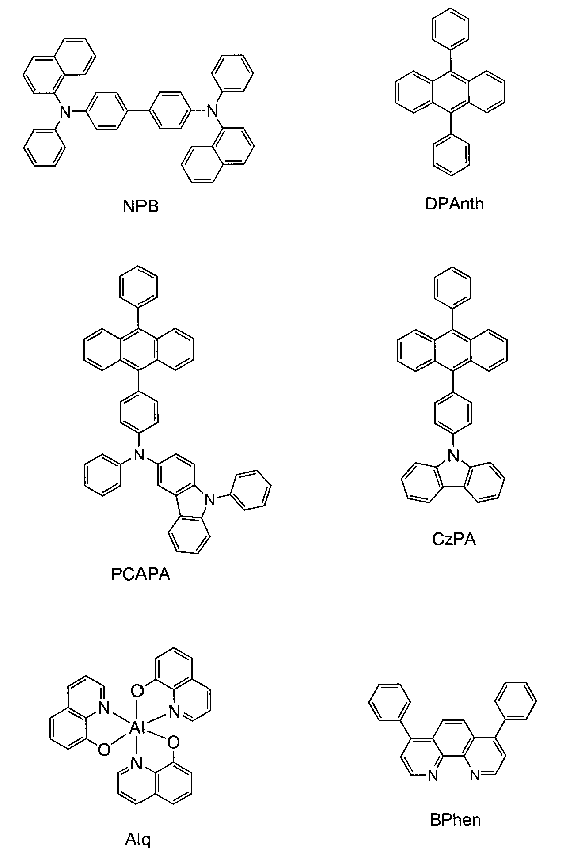
(발광소자 1)(Light emitting element 1)
우선, 유리 기판(2100B) 위에, 산화규소를 포함한 산화인듐-산화주석을 스퍼 터링법으로 성막하여, 제1 전극(2101B)을 형성했다. 이때, 그 막 두께는 110nm로 하고 전극면적은 2mm×2mm로 했다.First, indium oxide-tin oxide containing silicon oxide was formed on the
다음에 제1 전극(2101B)이 형성된 면이 아래쪽이 되도록, 제1 전극(2101B)이 형성된 기판을 진공증착 장치 내에 설치된 기판 홀더에 고정하고, 10-4Pa 정도까지 감압한 후, 제1 전극(2101B) 위에, 4,4'-비스[N-(1-나프틸)-N-페닐아미노]비페닐(약칭:NPB)과 산화몰리브덴(VI)을 공증착함으로써, 복합재료를 포함한 층(2111B)을 형성했다. 그 막 두께는 50nm로 하고 NPB와 산화몰리브덴(VI)의 비율은, 중량비로 4:1(=NPB:산화몰리브덴)이 되도록 조절했다. 이때, 공증착법이란, 하나의 처리실 내에서 복수의 증발원으로부터 동시에 증착을 행하는 증착법이다.Next, the substrate on which the
다음에 저항가열을 사용한 증착법에 의해, 4,4'-비스[N-(1-나프틸)-N-페닐아미노]비페닐(약칭:NPB)을 10nm의 막 두께가 되도록 성막하고, 정공수송층(2112B)을 형성했다.Next, a film of 4,4'-bis [N- (1-naphthyl) -N-phenylamino] biphenyl (abbreviation: NPB) was formed to a thickness of 10 nm by a vapor deposition method using resistance heating, (2112B).
다음에 정공수송층(2112B) 위에, 발광층(2113B)을 형성했다. 우선, 정공수송층(2112B) 위에, 9,10-디페닐 안트라센(약칭:DPAnth)과 N,9-디페닐-N-[4-(10-페닐-9-안트릴)페닐]-9H-카르바졸-3-아민(약칭:PCAPA)을 공증착함으로써, 제1 발광층(2121B)을 30nm의 막 두께로 형성했다. 여기에서, DPAnth와 PCAPA의 중량비는, 1:0.05(=DPAnth:PCAPA)가 되도록 조절했다. 또한, 제1 발광층(2121B) 위에, 9-[4-(10-페닐-9-안트릴)페닐]-9H-카르바졸(약칭:CzP A)과 PCAPA를 공증착함으로써, 제2 발광층(2122B)을 30nm의 막 두께로 형성했다. 여기에서, CzPA와 PCAPA의 중량비는, 1:0.05(=CzPA:PCAPA)가 되도록 조절했다.Next, a
그 후 저항가열에 의한 증착법을 사용하여, 발광층(2113B) 위에 전자수송층(2114B)을 형성했다. 우선, 트리스(8-퀴놀리노라토)알루미늄(약칭:Alq)을 10nm의 막 두께가 되도록 성막하고, 제1 전자수송층(2123B)을 형성했다. 또한, 제1 전자수송층(2123B) 위에, 바소페난트롤린(약칭:BPhen)을 20nm의 막 두께가 되도록 성막하고, 제2 전자수송층(2124B)을 형성했다.Thereafter, an
전자수송층(2114B) 위에, 불화 리튬(LiF)을 증착함으로써, 1nm의 막 두께의 전자주입층(2115B)을 형성했다.Lithium fluoride (LiF) was vapor-deposited on the electron-transporting
마지막으로, 저항가열에 의한 증착법을 사용하여, 알루미늄을 200nm의 막 두께가 되도록 성막함으로써, 제2 전극(2102B)을 형성하고, 발광소자 1을 제조했다.Finally, the
이상에 의해 얻어진 발광소자 1을, 질소분위기의 글로브 박스 내에서, 발광소자가 대기에 노출하지 않도록 밀봉하는 작업을 행한 후, 이들 발광소자의 동작 특성에 대해서 측정했다. 이때, 측정은 실온(25도로 유지된 분위기)에서 행했다.The
발광소자 1의 전류밀도-휘도 특성을 도 14에 나타낸다. 또한 전압-휘도 특성을 도 15에 나타낸다. 또한 휘도-전류 효율 특성을 도 16에 나타낸다. 또한 1mA의 전류를 흘려보냈을 때의 발광 스펙트럼을 도 17에 나타낸다. 또한 초기 휘도를 1000cd/m2로 했을 때의 발광소자 1의 규격화 휘도 시간변화를 도 18에 나타낸다.The current density-luminance characteristic of the light-emitting
발광소자 1은, 휘도 1120cd/m2일 때의 CIE 색도좌표는 (x=0.16, y=0.21)이며, 청색의 발광을 나타냈다. 또한 휘도 1120cd/m2일 때의 전압은 6.0V, 전류밀도는, 21.5mA/cm2였다. 또한 휘도 1120cd/m2일 때의 전류 효율은 5.2cd/A이며, 외부양자효율은 3.5%, 파워 효율은, 2.7lm/W이며, 고효율, 저소비 전력의 발광소자를 얻을 수 있었다. 또한 도 17로부터 발광 피크 파장은 469nm였다.The CIE chromaticity coordinates (x = 0.16, y = 0.21) of the light-emitting
또한 도 18로부터, 발광소자 1은, 통전 시작으로부터 1000시간 후에도 초기 휘도의 79%의 휘도를 유지하고 있어, 장수명 발광소자라는 것을 알 수 있다.It is also seen from Fig. 18 that the light-emitting
따라서, 본 발명을 적용함으로써, 장수명 발광소자를 얻을 수 있다는 것을 알았다.Therefore, it has been found that a long-lived light emitting device can be obtained by applying the present invention.
[실시예 2][Example 2]
본 실시예에서는, 본 발명의 발광장치에 사용하는 발광소자의 일례에 대해서 구체적으로 도 19를 사용하여 설명한다. 실시예 2에 사용하는 유기 화합물의 구조식을 이하에 나타낸다. 이때, 실시예 1에 사용한 재료에 대해서는 생략한다.In this embodiment, an example of a light emitting element used in the light emitting device of the present invention will be described specifically with reference to Fig. The structural formula of the organic compound used in Example 2 is shown below. At this time, the material used in Example 1 is omitted.
[화 35][35]
(발광소자 2)(Light emitting element 2)
우선, 유리 기판(2100G) 위에, 산화규소를 포함한 산화인듐-산화주석을 스퍼터링법으로 성막하여, 제1 전극(2101G)을 형성했다. 이때, 그 막 두께는 110nm로 하고 전극면적은 2mm×2mm로 했다.First, indium oxide-tin oxide containing silicon oxide was formed on the
다음에 제1 전극(2101G)이 형성된 면이 아래쪽이 되도록, 제1 전극(2101G)이 형성된 기판을 진공증착 장치 내에 설치된 기판 홀더에 고정하고, 10-4Pa 정도까지 감압한 후, 제1 전극(2101G) 위에, 4,4'-비스[N-(1-나프틸)-N-페닐아미노]비페닐(약칭:NPB)과 산화몰리브덴(VI)을 공증착함으로써, 복합재료를 포함한 층(2111G)을 형성했다. 그 막 두께는 50nm로 하고, NPB와 산화몰리브덴(VI)의 비율은, 중량비로 4:1(=NPB:산화몰리브덴)이 되도록 조절했다. 이때, 공증착법이란, 하나의 처리실 내에서 복수의 증발원으로부터 동시에 증착하는 증착법이다.Next, the substrate on which the
다음에 저항가열을 사용한 증착법에 의해, 4,4'-비스[N-(1-나프틸)-N-페닐아 미노]비페닐(약칭:NPB)을 10nm의 막 두께가 되도록 성막하여, 정공수송층(2112G)을 형성했다.Next, a film of 4,4'-bis [N- (1-naphthyl) -N-phenylamino] biphenyl (abbreviation: NPB) was formed to a thickness of 10 nm by evaporation using resistance heating, Thereby forming a
다음에 정공수송층(2112G) 위에, 발광층(2113G)을 형성했다. 우선, 정공수송층(2112G) 위에, 9-[4-(10-페닐-9-안트릴)페닐]-9H-카르바졸(약칭:CzPA)과 N-(9,10-디페닐-2-안트릴)-N,9-디페닐-9H-카르바졸-3-아민(약칭:2PCAPA)을 공증착함으로써, 발광층(2113G)을 30nm의 막 두께로 형성했다. 여기에서, CzPA와 2PCAPA의 중량비는, 1:0.05(=CzPA:2PCAPA)가 되도록 증착 레이트를 조절했다.Next, a
그리고, 발광층(2113G) 위에, 트리스(8-퀴놀리노라토)알루미늄(III)(약칭:Alq)과 N,N'-디페닐 퀴나크리돈(약칭:DPQd)을 공증착함으로써, 캐리어의 이동을 제어하는 층(2116G)을 10nm의 막 두께로 형성했다. 여기에서, Alq와 DPQd의 중량비는, 1:0.005(=Alq:DPQd)가 되도록 증착 레이트를 조절했다.Then, by co-depositing tris (8-quinolinolato) aluminum (III) (abbreviation: Alq) and N, N'-diphenylquinacridone (abbreviation: DPQd) on the
그 후 저항가열에 의한 증착법을 사용하여, 캐리어의 이동을 제어하는 층(2116G) 위에 바소페난트롤린(약칭:BPhen)을 30nm의 막 두께가 되도록 성막하여, 전자수송층(2114G)을 형성했다.Subsequently, a film of 30 nm thick was formed on the
전자수송층(2114G) 위에, 불화 리튬(LiF)을 1nm의 막 두께가 되도록 성막함으로써, 전자주입층(2115G)을 형성했다.On the
마지막으로, 저항가열에 의한 증착법을 사용하여, 알루미늄을 200nm의 막 두께가 되도록 성막함으로써, 제2 전극(2102G)을 형성하여, 발광소자 2를 제조했다.Finally, a
이상에 의해 얻어진 발광소자 2를, 질소분위기의 글로브 박스 내에서, 발광 소자가 대기에 노출하지 않도록 밀봉하는 작업을 행한 후, 이들 발광소자의 동작 특성에 대해서 측정했다. 이때, 측정은 실온(25도로 유지된 분위기)에서 행했다.The
발광소자 2의 전류밀도-휘도 특성을 도 20에 나타낸다. 또한 전압-휘도 특성을 도 21에 나타낸다. 또한 휘도-전류 효율 특성을 도 22에 나타낸다. 또한 1mA의 전류를 흘려보냈을 때의 발광 스펙트럼을 도 23에 나타낸다. 또한 초기 휘도를 5000cd/m2로 했을 때의 발광소자 2의 규격화 휘도 시간변화를 도 24에 나타낸다.The current density-luminance characteristic of the light-emitting
발광소자 2는, 휘도 4780cd/m2일 때의 CIE 색도좌표는 (x=0.30, y=0.61)이며, 녹색의 발광을 나타냈다. 또한 휘도 4780cd/m2일 때의 전압은 5.6V, 전류밀도는, 36.5mA/cm2이었다. 또한 휘도 4780cd/m2일 때의 전류 효율은 13cd/A이며, 외부양자효율은 3.8%, 파워 효율은, 7.3lm/W이며, 고효율, 저소비 전력의 발광소자를 얻을 수 있었다. 또한 도 23으로부터 발광 피크 파장은, 517nm이었다.The CIE chromaticity coordinates (x = 0.30, y = 0.61) of the
또한 도 24로부터, 발광소자 2는, 통전 시작으로부터 1000시간 후에도 초기 휘도의 88%의 휘도를 유지하고 있어, 장수명 발광소자라는 것을 알 수 있다.It is also seen from Fig. 24 that the
따라서, 본 발명을 적용함으로써, 장수명 발광소자를 얻을 수 있다는 것을 알았다.Therefore, it has been found that a long-lived light emitting device can be obtained by applying the present invention.
[실시예 3][Example 3]
본 실시예에서는, 본 발명의 발광장치가 사용하는 발광소자의 일례에 대해서 구체적으로 도 25를 사용하여 설명한다. 본 실시예에서 사용하는 유기 화합물의 구 조식을 이하에 나타낸다. 이때, 실시예 1 또는 실시예 2에 사용한 재료에 대해서는 생략한다.In this embodiment, an example of a light emitting element used by the light emitting device of the present invention will be described specifically with reference to Fig. The structure of the organic compound used in this example is shown below. At this time, the materials used in Example 1 or Example 2 are omitted.
[화 36][36]

(발광소자 3)(Light emitting element 3)
우선, 유리 기판(2100R) 위에, 산화규소를 포함한 산화인듐-산화주석을 스퍼터링법으로 성막하여, 제1 전극(2101R)을 형성했다. 이때, 그 막 두께는 110nm로 하고, 전극면적은 2mm×2mm로 했다.First, indium oxide-tin oxide containing silicon oxide was formed on the
다음에 제1 전극(2101R)이 형성된 면이 아래쪽이 되도록, 제1 전극(2101R)이 형성된 기판을 진공증착 장치 내에 설치된 기판 홀더에 고정하고, 10-4Pa 정도까지 감압한 후, 제1 전극(2101R) 위에, 4,4'-비스[N-(1-나프틸)-N-페닐아미노]비페닐(약칭:NPB)과 산화몰리브덴(VI)을 공증착함으로써, 복합재료를 포함한 층(2111R)을 형성했다. 그 막 두께는 50nm로 하고, NPB와 산화몰리브덴(VI)의 비율은, 중량비로 4:1(=NPB:산화몰리브덴)이 되도록 조절했다. 이때, 공증착법이란, 하나의 처리실 내에서 복수의 증발원으로부터 동시에 증착하는 증착법이다.Next, the substrate on which the
다음에 저항가열을 사용한 증착법에 의해, 4,4'-비스[N-(1-나프틸)-N-페닐아미노]비페닐(약칭:NPB)을 10nm의 막 두께가 되도록 성막하여, 정공수송층(2112R)을 형성했다.Next, a film of 4,4'-bis [N- (1-naphthyl) -N-phenylamino] biphenyl (abbreviation: NPB) was formed to a thickness of 10 nm by a vapor deposition method using resistance heating, (2112R).
다음에 정공수송층(2112R) 위에, 발광층(2113R)을 형성했다. 우선, 정공수송성 유기 화합물로서 NPB를, 전자수송성 유기 화합물로서 비스(2-메틸-8-퀴놀리노라토)(4-페닐페놀라토)알루미늄(III)(약칭:BAlq)을, 피라진계 유기 금속착체로서 (아세틸아세토나토)비스(2,3,5-트리페닐피라지나토)이리듐(III)(약칭: [Ir(tppr)2(acac)]을 사용하고, 질량비가 NPB:BAlq:Ir(tppr)2(acac)=0.1:1:0.06이 되도록 공증착을 행했다. 막 두께는 50nm로 했다.Next, a
그 후 저항가열에 의한 증착법을 사용하여, 발광층(2113R) 위에 전자수송층(2114R)을 형성했다. 우선, 트리스(8-퀴놀리노라토)알루미늄(약칭:Alq)을 10nm의 막 두께가 되도록 성막하여, 제1 전자수송층(2123R)을 형성했다. 또한, 제1 전자수송층(2123R) 위에, 바소페난트롤린(약칭:BPhen)을 20nm의 막 두께가 되도록 성막하여, 제2 전자수송층(2124R)을 형성했다.Thereafter, an
전자수송층(2114R) 위에, 불화 리튬(LiF)을 증착함으로써, 1nm의 막 두께의 전자주입층(2115R)을 형성했다.Lithium fluoride (LiF) was deposited on the
마지막으로, 저항가열에 의한 증착법을 사용하여, 알루미늄을 200nm의 막 두 께가 되도록 성막함으로써, 제2 전극(2102R)을 형성하여, 발광소자 3을 제조했다.Finally, a
이상에 의해 얻어진 발광소자 3을, 질소분위기의 글로브 박스 내에서, 발광소자가 대기에 노출하지 않도록 밀봉하는 작업을 행한 후, 이들 발광소자의 동작 특성에 대해서 측정했다. 이때, 측정은 실온(25도로 유지된 분위기)에서 행했다.The
발광소자 3의 전류밀도-휘도 특성을 도 26에 나타낸다. 또한 전압-휘도 특성을 도 27에 나타낸다. 또한 휘도-전류 효율 특성을 도 28에 나타낸다. 또한 1mA의 전류를 흘려보냈을 때의 발광 스펙트럼을 도 29에 나타낸다. 또한 초기 휘도를 1000cd/m2로 했을 때의 발광소자 3의 규격화 휘도 시간변화를 도 30에 나타낸다.The current density-luminance characteristic of the light-emitting
발광소자 3은, 휘도 1160cd/m2일 때의 CIE 색도좌표는 (x=0.65, y=0.35)이며, 적색의 발광을 나타냈다. 또한 휘도 1160cd/m2일 때의 전압은 7.0V, 전류밀도는, 4.59mA/cm2이었다. 또한 휘도 1160cd/m2일 때의 전류 효율은 25cd/A이며, 외부양자효율은 20%, 파워 효율은, 11lm/W이며, 고효율, 저소비 전력의 발광소자를 얻을 수 있었다. 또한 도 29로부터 발광 피크 파장은, 619nm이었다.The luminous means 3 had CIE chromaticity coordinates (x = 0.65, y = 0.35) at a luminance of 1160 cd / m < 2 > The voltage at a luminance of 1160 cd / m < 2 > was 7.0 V and the current density was 4.59 mA / cm < 2 & gt ;. The current efficiency at the luminance of 1160 cd / m 2 was 25 cd / A, the external quantum efficiency was 20%, and the power efficiency was 11 lm / W. Thus, a light emitting device with high efficiency and low power consumption was obtained. 29, the emission peak wavelength was 619 nm.
또한 도 30으로부터, 발광소자 3은, 통전 시작으로부터 1000시간 후에도 초기 휘도의 94%의 휘도를 유지하고 있어, 장수명 발광소자라는 것을 알 수 있다.It is also seen from Fig. 30 that the light-emitting
따라서, 본 발명을 적용함으로써, 장수명 발광소자를 얻을 수 있다는 것을 알았다.Therefore, it has been found that a long-lived light emitting device can be obtained by applying the present invention.
도 1은 본 발명의 발광장치를 설명하는 도면.BRIEF DESCRIPTION OF THE DRAWINGS FIG.
도 2는 본 발명의 발광장치를 설명하는 도면.2 is a view for explaining a light emitting device of the present invention.
도 3은 본 발명의 발광장치를 설명하는 도면.3 is a view for explaining a light emitting device of the present invention.
도 4는 본 발명의 발광장치를 설명하는 도면.4 is a view for explaining a light emitting device of the present invention.
도 5는 본 발명의 발광장치를 설명하는 도면.5 is a view for explaining a light emitting device of the present invention.
도 6은 본 발명의 발광장치를 설명하는 도면.6 is a view for explaining a light emitting device of the present invention.
도 7은 본 발명의 발광장치를 설명하는 도면.7 is a view for explaining the light emitting device of the present invention.
도 8은 본 발명의 발광장치를 설명하는 도면.8 is a view for explaining the light emitting device of the present invention.
도 9는 본 발명의 발광장치를 설명하는 도면.9 is a view for explaining a light emitting device of the present invention.
도 10은 본 발명의 발광장치를 설명하는 도면.10 is a view for explaining a light emitting device of the present invention.
도 11은 본 발명의 전자기기를 설명하는 도면.11 is a view for explaining an electronic apparatus of the present invention.
도 12는 본 발명의 발광장치를 설명하는 도면.12 is a view for explaining a light emitting device of the present invention.
도 13은 실시예 1의 발광소자를 설명하는 도면.13 is a view for explaining a light emitting element of
도 14는 실시예 1에서 제조한 발광소자의 전류밀도-휘도 특성을 도시한 도면.14 is a graph showing current density-luminance characteristics of the light emitting device manufactured in Example 1. Fig.
도 15는 실시예 1에서 제조한 발광소자의 전압-휘도 특성을 도시한 도면.15 is a graph showing voltage-luminance characteristics of the light emitting device manufactured in Example 1. Fig.
도 16은 실시예 1에서 제조한 발광소자의 휘도-전류 효율 특성을 도시한 도면.16 is a graph showing luminance-current efficiency characteristics of the light emitting device manufactured in Example 1. Fig.
도 17은 실시예 1에서 제조한 발광소자의 발광 스펙트럼을 도시한 도면.17 is a view showing an emission spectrum of the light emitting device manufactured in Example 1. Fig.
도 18은 실시예 1에서 제조한 발광소자의 규격화 휘도 시간변화를 도시한 도면.18 is a view showing a change over time of normalized luminance of the light emitting device manufactured in Example 1. Fig.
도 19는 실시예 2의 발광소자를 설명하는 도면.19 is a view for explaining a light emitting element of
도 20은 실시예 2에서 제조한 발광소자의 전류밀도-휘도 특성을 도시한 도면.20 is a graph showing current density-luminance characteristics of the light emitting device manufactured in Example 2. Fig.
도 21은 실시예 2에서 제조한 발광소자의 전압-휘도 특성을 도시한 도면.21 is a graph showing voltage-luminance characteristics of the light emitting device manufactured in Example 2. Fig.
도 22는 실시예 2에서 제조한 발광소자의 휘도-전류 효율 특성을 도시한 도면.22 is a graph showing luminance-current efficiency characteristics of the light emitting device manufactured in Example 2. Fig.
도 23은 실시예 2에서 제조한 발광소자의 발광 스펙트럼을 도시한 도면.23 is a diagram showing the emission spectrum of the light emitting device manufactured in Example 2. Fig.
도 24는 실시예 2에서 제조한 발광소자의 규격화 휘도 시간변화를 도시한 도면.24 is a view showing a change over time of normalized luminance of the light emitting device manufactured in Example 2. Fig.
도 25는 실시예 3의 발광소자를 설명하는 도면.25 is a view for explaining a light-emitting element of
도 26은 실시예 3에서 제조한 발광소자의 전류밀도-휘도 특성을 도시한 도면.26 is a graph showing current density-luminance characteristics of the light emitting device manufactured in Example 3. Fig.
도 27은 실시예 3에서 제조한 발광소자의 전압-휘도 특성을 도시한 도면.27 is a view showing voltage-luminance characteristics of the light emitting device manufactured in Example 3. Fig.
도 28은 실시예 3에서 제조한 발광소자의 휘도-전류 효율 특성을 도시한 도면.28 is a graph showing luminance-current efficiency characteristics of the light emitting device manufactured in Example 3. Fig.
도 29는 실시예 3에서 제조한 발광소자의 발광 스펙트럼을 도시한 도면.29 is a diagram showing an emission spectrum of the light emitting device manufactured in Example 3. Fig.
도 30은 실시예 3에서 제조한 발광소자의 규격화 휘도 시간변화를 도시한 도면.30 is a view showing a change over time of normalized luminance of the light emitting device manufactured in Example 3. Fig.
[부호의 설명][Description of Symbols]
100 기판 101 양극100 substrate 101 anode
102 음극 103 EL층102 cathode 103 EL layer
113 발광층 116 캐리어의 이동을 제어하는 층113 Emissive layer 116 Layer controlling the movement of carriers
121 제1 발광층 122 제2 발광층121 First
131 발광 영역 211 제5 유기 화합물의 HOMO 준위131
212 제5 유기 화합물의 LUMO 준위 221 제6 유기 화합물의 HOMO 준위212 LUMO level of the fifth
222 제6 유기 화합물의 LUMO 준위222 LUMO level of the sixth organic compound
231 피라진계 유기 금속착체의 HOMO 준위HOMO level of pyrazine type organometallic complex
232 피라진계 유기 금속착체의 LUMO 준위232 LUMO level of pyrazine type organometallic complex
601 소스측 구동회로 602 화소부601 Source
603 게이트측 구동회로 604 밀봉기판603 gate
605 씰재 607 공간605
608 배선 609 FPC(플랙시블 프린트 서킷)608
610 소자기판 611 스위칭용 TFT610
612 전류제어용 TFT 613 제1 전극612
614 절연물 616 EL층614
617 제2 전극 618 발광소자617
623 N채널형 TFT 624 P채널형 TFT623 N-channel type TFT 624 P-channel type TFT
910 기판 911 트랜지스터910 substrate 911 transistor
912 발광소자 913 제1 전극912 Light emitting element 913 First electrode
914 제2 전극 915 EL층914 Second electrode 915 EL layer
916 층간 절연막 917 배선916 Interlayer insulating film 917 Wiring
918 분리벽층 919 층간 절연막918 Separation wall layer 919 Interlayer insulating film
951 기판 952 전극951
953 절연층 954 분리벽층953
955 유기층 956 전극955
101B 양극 101G 양극
101R 양극 102B 음극
102G 음극 102R 음극
103B EL층 103G EL층
103R EL층 1100 기판
1101 양극 1102 음극1101
1111 정공주입층 1112 정공수송층1111
1114 전자수송층 1115 전자주입층1114
111B 정공주입층 111G 정공주입층111B
111R 정공주입층 112B 정공수송층111R
112G 정공수송층 112R 정공수송층112G
113B 발광층 113G 발광층113B
113R 발광층 114B 전자수송층113R Light-emitting
114G 전자수송층 114R 전자수송층114G
115B 전자주입층 115G 전자주입층115B
115R 전자주입층 116G 캐리어의 이동을 제어하는 층115R
131B 발광 영역 131G 발광 영역131B
131R 발광 영역 1401 스위칭용 TFT131R
1402 용량소자 1403 구동용 TFT1402
1404 전류제어용 TFT 1405 발광소자1404
1406 TFT 1410 신호선1406
1411 전원선 1412 전원선1411
1414 주사선 1415 주사선1414
1500 화소부 1554 공통 전위선1500
1561 다이오드 9101 케이싱1561
9102 지지대 9103 표시부9102
9104 스피커부 9105 비디오 입력 단자9104
916a 층간 절연막 916b 층간 절연막916a Interlayer insulating
916c 층간 절연막 9201 본체916c
9202 케이싱 9203 표시부9202
9204 키보드 9205 외부접속 포트9204
9206 포인팅 디바이스 9401 본체9206
9402 케이싱 9403 표시부9402
9404 음성입력부 9405 음성출력부9404
9406 조작키 9407 외부접속 포트9406
9408 안테나 9501 본체9408
9502 표시부 9503 케이싱9502
9504 외부접속 포트 9505 리모트 컨트롤 수신부9504
9506 수상부 9507 배터리9506
9508 음성입력부 9509 조작키9508
9510 접안부 1113B 발광층9510
1113G 발광층 1113R 발광층1113G
1116G 캐리어의 이동을 제어하는 층Layer controlling the movement of the 1116G carrier
1121B 제1 발광층 1122B 제2 발광층1121B First
1131B 발광 영역 1131G 발광 영역1131B
1131R 발광 영역 2100B 유리 기판1131R
2100G 유리 기판 2100R 유리기판
2101B 제1 전극 2101G 제1 전극
2101R 제1 전극 2102B 제2 전극2101R
2102G 제2 전극 2102R 제2 전극
2111B 복합재료를 포함한 층 2111G 복합재료를 포함한 층Layer containing 2111B composite material Layer containing 2111G composite material
2111R 복합재료를 포함한 층 2112B 정공수송층2111R layer containing a
2112G 정공수송층 2112R 정공수송층2112G
2113B 발광층 2113G 발광층2113B
2113R 발광층 2114B 전자수송층2113R
2114G 전자수송층 2114R 전자수송층2114G
2115B 전자주입층 2115G 전자주입층2115B
2115R 전자주입층 2116G 캐리어의 이동을 제어하는 층2115R
2121B 제1 발광층 2122B 제2 발광층2121B First
2123B 제1 전자수송층 2123R 제1 전자수송층2123B First
2124B 제2 전자수송층 2124R 제2 전자수송층2124B Second
Claims (20)
Applications Claiming Priority (2)
| Application Number | Priority Date | Filing Date | Title |
|---|---|---|---|
| JP2007077833 | 2007-03-23 | ||
| JPJP-P-2007-00077833 | 2007-03-23 |
Publications (2)
| Publication Number | Publication Date |
|---|---|
| KR20080086825A KR20080086825A (en) | 2008-09-26 |
| KR101401527B1 true KR101401527B1 (en) | 2014-06-03 |
Family
ID=39561699
Family Applications (1)
| Application Number | Title | Priority Date | Filing Date |
|---|---|---|---|
| KR1020080025841A Expired - Fee Related KR101401527B1 (en) | 2007-03-23 | 2008-03-20 | Light-emitting device and electronic device |
Country Status (4)
| Country | Link |
|---|---|
| US (1) | US8053980B2 (en) |
| EP (1) | EP1973386B8 (en) |
| JP (2) | JP4974941B2 (en) |
| KR (1) | KR101401527B1 (en) |
Families Citing this family (37)
| Publication number | Priority date | Publication date | Assignee | Title |
|---|---|---|---|---|
| EP1928828B1 (en) * | 2005-09-02 | 2012-03-14 | Semiconductor Energy Laboratory Co., Ltd. | Anthracene derivative |
| CN101931056B (en) * | 2006-06-01 | 2014-07-09 | 株式会社半导体能源研究所 | Light-emitting element, light-emitting device and an electronic device |
| EP1876658A3 (en) * | 2006-07-04 | 2014-06-25 | Semiconductor Energy Laboratory Co., Ltd. | Light-emitting element, light-emitting device, and electronic device |
| WO2008038607A1 (en) * | 2006-09-28 | 2008-04-03 | Semiconductor Energy Laboratory Co., Ltd. | Anthracene derivative, and light emitting element, light emitting device, and electronic device using the anthracene derivative |
| KR101426717B1 (en) * | 2006-12-04 | 2014-08-06 | 가부시키가이샤 한도오따이 에네루기 켄큐쇼 | Light emitting device, light emitting device and electronic device |
| US9397308B2 (en) | 2006-12-04 | 2016-07-19 | Semiconductor Energy Laboratory Co., Ltd. | Light emitting element, light emitting device, and electronic device |
| WO2009051248A1 (en) * | 2007-10-19 | 2009-04-23 | Semiconductor Energy Laboratory Co., Ltd. | Light-emitting element, light-emitting device, and electronic device |
| EP2075860A3 (en) * | 2007-12-28 | 2013-03-20 | Semiconductor Energy Laboratory Co., Ltd. | Light-emitting element, light-emitting device and electronic device |
| KR101587867B1 (en) * | 2008-03-18 | 2016-01-22 | 가부시키가이샤 한도오따이 에네루기 켄큐쇼 | Light-emitting element, light-emitting device and electronic device |
| WO2009116547A1 (en) * | 2008-03-18 | 2009-09-24 | Semiconductor Energy Laboratory Co., Ltd. | Light-emitting element, light-emitting device and electronic device |
| CN105957972A (en) * | 2008-05-16 | 2016-09-21 | 株式会社半导体能源研究所 | Light-emitting element, electronic device, light-emitting device |
| JP2010114425A (en) * | 2008-10-10 | 2010-05-20 | Canon Inc | Organic el display device |
| US8581237B2 (en) * | 2008-12-17 | 2013-11-12 | Semiconductor Energy Laboratory Co., Ltd. | Light-emitting element |
| TWI528862B (en) * | 2009-01-21 | 2016-04-01 | 半導體能源研究所股份有限公司 | Light-emitting element, light-emitting device and electronic device |
| JP5514451B2 (en) * | 2009-02-27 | 2014-06-04 | 大日本印刷株式会社 | Organic electroluminescence device |
| WO2010137509A1 (en) * | 2009-05-29 | 2010-12-02 | Semiconductor Energy Laboratory Co., Ltd. | Light-emitting element, light-emitting device, lighting device, and electronic appliance |
| KR101691395B1 (en) * | 2009-09-04 | 2017-01-02 | 가부시키가이샤 한도오따이 에네루기 켄큐쇼 | Light-emitting element, light-emitting device, and method for manufacturing the same |
| JP2011139044A (en) * | 2009-12-01 | 2011-07-14 | Semiconductor Energy Lab Co Ltd | Luminous element, luminous device, electronic equipment, and lighting device |
| JP5829828B2 (en) | 2010-04-06 | 2015-12-09 | 株式会社半導体エネルギー研究所 | Organometallic complex, light emitting element and light emitting device |
| KR101880183B1 (en) | 2011-02-11 | 2018-07-19 | 가부시키가이샤 한도오따이 에네루기 켄큐쇼 | Light-emitting device and display device |
| WO2013008765A1 (en) * | 2011-07-08 | 2013-01-17 | Semiconductor Energy Laboratory Co., Ltd. | Light-emitting module, light-emitting device, and method for manufacturing the light-emitting module |
| JP2015215940A (en) * | 2012-08-17 | 2015-12-03 | 出光興産株式会社 | LIGHT EMITTING DEVICE, ELECTRONIC DEVICE, AND METHOD FOR MANUFACTURING LIGHT EMITTING DEVICE |
| KR102178256B1 (en) * | 2013-03-27 | 2020-11-12 | 가부시키가이샤 한도오따이 에네루기 켄큐쇼 | Light-emitting element, light-emitting device, electronic appliance, and lighting device |
| JP2016072250A (en) * | 2014-09-30 | 2016-05-09 | 株式会社半導体エネルギー研究所 | Light-emitting device, electronic equipment, and lighting device |
| KR102357440B1 (en) * | 2015-01-05 | 2022-02-03 | 삼성디스플레이 주식회사 | Organic light emitting display and manufacturing method thereof |
| TWI737594B (en) * | 2015-03-09 | 2021-09-01 | 日商半導體能源研究所股份有限公司 | Light-emitting element, display device, electronic device, and lighting device |
| TWI860824B (en) * | 2015-03-09 | 2024-11-01 | 日商半導體能源研究所股份有限公司 | Light-emitting element, display device, electronic device, and lighting device |
| KR102623039B1 (en) * | 2015-05-15 | 2024-01-08 | 가부시키가이샤 한도오따이 에네루기 켄큐쇼 | Light-emitting element, light-emitting device, electronic device, and lighting device |
| CN104900684B (en) * | 2015-06-12 | 2018-01-30 | 京东方科技集团股份有限公司 | Display base plate and preparation method thereof, display device |
| US10249839B2 (en) | 2016-07-20 | 2019-04-02 | Joled Inc. | Organic electroluminescence device, organic electroluminescence unit, and electronic apparatus |
| US10797256B2 (en) | 2016-07-20 | 2020-10-06 | Joled Inc. | Organic electroluminescence device, organic electroluminescence unit, and electronic apparatus |
| US10062860B2 (en) | 2016-07-20 | 2018-08-28 | Joled Inc. | Organic electroluminescence device, organic electroluminescence unit, and electronic apparatus |
| US10950805B2 (en) | 2017-05-19 | 2021-03-16 | Semiconductor Energy Laboratory Co., Ltd. | Electronic device, light-emitting device, electronic appliance, and lighting device |
| US10784456B2 (en) | 2017-06-06 | 2020-09-22 | Joled Inc. | Organic electroluminescent unit |
| KR102317452B1 (en) * | 2017-10-19 | 2021-10-28 | 삼성디스플레이 주식회사 | Light-emitting device |
| CN108550707B (en) * | 2018-04-12 | 2022-11-08 | 京东方科技集团股份有限公司 | Quantum dot light-emitting diodes, liquid crystal display devices |
| CN109065762A (en) * | 2018-08-01 | 2018-12-21 | 武汉华星光电半导体显示技术有限公司 | The production method and OLED device of OLED device |
Citations (4)
| Publication number | Priority date | Publication date | Assignee | Title |
|---|---|---|---|---|
| KR20030020034A (en) * | 2001-08-29 | 2003-03-08 | 엘지.필립스 엘시디 주식회사 | The organic electro-luminescence device |
| KR20040023781A (en) * | 2002-09-11 | 2004-03-18 | 옵토 테크 코포레이션 | Organic electroluminescnet device and method for producing the same |
| US6734457B2 (en) | 2001-11-27 | 2004-05-11 | Semiconductor Energy Laboratory Co., Ltd. | Light emitting device |
| US6803720B2 (en) | 2000-12-15 | 2004-10-12 | Universal Display Corporation | Highly stable and efficient OLEDs with a phosphorescent-doped mixed layer architecture |
Family Cites Families (50)
| Publication number | Priority date | Publication date | Assignee | Title |
|---|---|---|---|---|
| JPH06158038A (en) | 1992-11-17 | 1994-06-07 | Pioneer Electron Corp | Organic electroluminescent element |
| JP3949214B2 (en) * | 1997-03-18 | 2007-07-25 | 出光興産株式会社 | Organic electroluminescence device |
| JP2000068057A (en) | 1998-06-12 | 2000-03-03 | Idemitsu Kosan Co Ltd | Organic electroluminescence device |
| JP2001052870A (en) * | 1999-06-03 | 2001-02-23 | Tdk Corp | Organic electroluminescent element |
| JP4382961B2 (en) | 2000-05-02 | 2009-12-16 | 富士フイルム株式会社 | Light emitting element |
| JP2002062824A (en) | 2000-06-05 | 2002-02-28 | Semiconductor Energy Lab Co Ltd | Light emitting device |
| US7339317B2 (en) | 2000-06-05 | 2008-03-04 | Semiconductor Energy Laboratory Co., Ltd. | Light-emitting device having triplet and singlet compound in light-emitting layers |
| JP4948740B2 (en) * | 2000-08-24 | 2012-06-06 | ノバルティス アーゲー | Method for surface modification of substrate and modified substrate obtained therefrom |
| SG138466A1 (en) | 2000-12-28 | 2008-01-28 | Semiconductor Energy Lab | Luminescent device |
| TW545080B (en) | 2000-12-28 | 2003-08-01 | Semiconductor Energy Lab | Light emitting device and method of manufacturing the same |
| TW518909B (en) | 2001-01-17 | 2003-01-21 | Semiconductor Energy Lab | Luminescent device and method of manufacturing same |
| TW519770B (en) | 2001-01-18 | 2003-02-01 | Semiconductor Energy Lab | Light emitting device and manufacturing method thereof |
| TW552650B (en) | 2001-02-01 | 2003-09-11 | Semiconductor Energy Lab | Deposition apparatus and deposition method |
| SG118110A1 (en) | 2001-02-01 | 2006-01-27 | Semiconductor Energy Lab | Organic light emitting element and display device using the element |
| US20030010288A1 (en) | 2001-02-08 | 2003-01-16 | Shunpei Yamazaki | Film formation apparatus and film formation method |
| TW582121B (en) | 2001-02-08 | 2004-04-01 | Semiconductor Energy Lab | Light emitting device |
| TW550672B (en) | 2001-02-21 | 2003-09-01 | Semiconductor Energy Lab | Method and apparatus for film deposition |
| SG118118A1 (en) | 2001-02-22 | 2006-01-27 | Semiconductor Energy Lab | Organic light emitting device and display using the same |
| EP1388903B1 (en) | 2002-08-09 | 2016-03-16 | Semiconductor Energy Laboratory Co., Ltd. | Organic electroluminescent device |
| JP4287198B2 (en) | 2002-11-18 | 2009-07-01 | 出光興産株式会社 | Organic electroluminescence device |
| JP2004273163A (en) | 2003-03-05 | 2004-09-30 | Sony Corp | Organic EL element, manufacturing method thereof, and organic EL panel |
| JP2004335122A (en) * | 2003-04-30 | 2004-11-25 | Takasago Internatl Corp | Light emitting element |
| JP2005011734A (en) | 2003-06-20 | 2005-01-13 | Sony Corp | Display element and display device |
| JP4479171B2 (en) | 2003-06-20 | 2010-06-09 | ソニー株式会社 | Display element |
| TW200527956A (en) | 2003-10-24 | 2005-08-16 | Pentax Corp | White organic electroluminescent device |
| CN101859877A (en) * | 2003-12-02 | 2010-10-13 | 株式会社半导体能源研究所 | Light-emitting elements, light-emitting devices, and electrical equipment |
| TW200541401A (en) | 2004-02-13 | 2005-12-16 | Idemitsu Kosan Co | Organic electroluminescent device |
| JP2005235403A (en) | 2004-02-17 | 2005-09-02 | Hitachi Displays Ltd | Organic EL display device |
| JPWO2005091686A1 (en) * | 2004-03-19 | 2008-02-07 | チッソ株式会社 | Organic electroluminescence device |
| JP4947909B2 (en) * | 2004-03-25 | 2012-06-06 | 三洋電機株式会社 | Organic electroluminescence device |
| JP4393249B2 (en) | 2004-03-31 | 2010-01-06 | 株式会社 日立ディスプレイズ | ORGANIC LIGHT EMITTING ELEMENT, IMAGE DISPLAY DEVICE, AND MANUFACTURING METHOD THEREOF |
| JP4366332B2 (en) | 2004-04-02 | 2009-11-18 | 株式会社半導体エネルギー研究所 | Organometallic complex, light emitting element and light emitting device using the organometallic complex |
| US8084145B2 (en) * | 2004-04-02 | 2011-12-27 | Semiconductor Energy Laboratory Co., Ltd. | Organometallic complex, light emitting element using the complex, light emitting device using the element, and electric apparatus using the device |
| JP4916137B2 (en) * | 2004-07-29 | 2012-04-11 | 三洋電機株式会社 | Organic electroluminescence device |
| JP2006049057A (en) | 2004-08-04 | 2006-02-16 | Hitachi Displays Ltd | Organic EL display device |
| US7579090B2 (en) * | 2004-09-20 | 2009-08-25 | Eastman Kodak Company | Organic element for electroluminescent devices |
| US7952089B2 (en) | 2004-10-22 | 2011-05-31 | Semiconductor Energy Laboratory Co., Ltd. | Composite material and light emitting element |
| US20070262693A1 (en) | 2004-10-29 | 2007-11-15 | Satoshi Seo | Composite Material, Light-Emitting Element, Light-Emitting Device and Manufacturing Method Thereof |
| WO2006049334A1 (en) * | 2004-11-05 | 2006-05-11 | Semiconductor Energy Laboratory Co., Ltd. | Light emitting element and light emitting device using the same |
| KR100669757B1 (en) * | 2004-11-12 | 2007-01-16 | 삼성에스디아이 주식회사 | Organic electroluminescent element |
| JP4653469B2 (en) | 2004-12-01 | 2011-03-16 | 出光興産株式会社 | Organic electroluminescence device |
| JP4496948B2 (en) * | 2004-12-13 | 2010-07-07 | 株式会社豊田自動織機 | Organic EL device |
| JP4533796B2 (en) * | 2005-05-06 | 2010-09-01 | 富士フイルム株式会社 | Organic electroluminescence device |
| JP2007042875A (en) * | 2005-08-03 | 2007-02-15 | Fujifilm Holdings Corp | Organic electroluminescence element |
| JP2007077833A (en) | 2005-09-12 | 2007-03-29 | Toshiba Corp | Turbine |
| US8920941B2 (en) | 2005-12-28 | 2014-12-30 | Semiconductor Energy Laboratory Co., Ltd. | Pyrazine derivative, and light emitting element, display device, electronic device using the pyrazine derivative |
| CN101931056B (en) * | 2006-06-01 | 2014-07-09 | 株式会社半导体能源研究所 | Light-emitting element, light-emitting device and an electronic device |
| EP1863105B1 (en) | 2006-06-02 | 2020-02-19 | Semiconductor Energy Laboratory Co., Ltd. | Light-emitting element, light-emitting device, and electronic device |
| EP1876658A3 (en) * | 2006-07-04 | 2014-06-25 | Semiconductor Energy Laboratory Co., Ltd. | Light-emitting element, light-emitting device, and electronic device |
| EP2087063B1 (en) * | 2006-11-30 | 2016-10-19 | Semiconductor Energy Laboratory Co, Ltd. | Light-emitting device |
-
2008
- 2008-03-10 EP EP08004409.2A patent/EP1973386B8/en not_active Not-in-force
- 2008-03-14 US US12/048,516 patent/US8053980B2/en not_active Expired - Fee Related
- 2008-03-19 JP JP2008071139A patent/JP4974941B2/en active Active
- 2008-03-20 KR KR1020080025841A patent/KR101401527B1/en not_active Expired - Fee Related
-
2012
- 2012-04-10 JP JP2012089422A patent/JP5572177B2/en not_active Expired - Fee Related
Patent Citations (4)
| Publication number | Priority date | Publication date | Assignee | Title |
|---|---|---|---|---|
| US6803720B2 (en) | 2000-12-15 | 2004-10-12 | Universal Display Corporation | Highly stable and efficient OLEDs with a phosphorescent-doped mixed layer architecture |
| KR20030020034A (en) * | 2001-08-29 | 2003-03-08 | 엘지.필립스 엘시디 주식회사 | The organic electro-luminescence device |
| US6734457B2 (en) | 2001-11-27 | 2004-05-11 | Semiconductor Energy Laboratory Co., Ltd. | Light emitting device |
| KR20040023781A (en) * | 2002-09-11 | 2004-03-18 | 옵토 테크 코포레이션 | Organic electroluminescnet device and method for producing the same |
Also Published As
| Publication number | Publication date |
|---|---|
| JP5572177B2 (en) | 2014-08-13 |
| EP1973386B1 (en) | 2015-11-11 |
| JP2008270770A (en) | 2008-11-06 |
| JP4974941B2 (en) | 2012-07-11 |
| EP1973386A2 (en) | 2008-09-24 |
| US8053980B2 (en) | 2011-11-08 |
| JP2012134569A (en) | 2012-07-12 |
| EP1973386A3 (en) | 2009-12-02 |
| KR20080086825A (en) | 2008-09-26 |
| US20080231177A1 (en) | 2008-09-25 |
| EP1973386B8 (en) | 2016-01-13 |
Similar Documents
| Publication | Publication Date | Title |
|---|---|---|
| KR101401527B1 (en) | Light-emitting device and electronic device | |
| KR102800073B1 (en) | Light-emitting element, light-emitting device, and electronic appliance | |
| KR101663000B1 (en) | Light-emitting element and light-emitting device | |
| KR101424694B1 (en) | Light-emitting element and electronic device | |
| KR101434277B1 (en) | Light emitting device, light emitting device and electronic device | |
| CN101803058B (en) | Light-emitting element, light-emitting device, and electronic device |
Legal Events
| Date | Code | Title | Description |
|---|---|---|---|
| PA0109 | Patent application |
St.27 status event code: A-0-1-A10-A12-nap-PA0109 |
|
| PG1501 | Laying open of application |
St.27 status event code: A-1-1-Q10-Q12-nap-PG1501 |
|
| R17-X000 | Change to representative recorded |
St.27 status event code: A-3-3-R10-R17-oth-X000 |
|
| A201 | Request for examination | ||
| E13-X000 | Pre-grant limitation requested |
St.27 status event code: A-2-3-E10-E13-lim-X000 |
|
| P11-X000 | Amendment of application requested |
St.27 status event code: A-2-2-P10-P11-nap-X000 |
|
| P13-X000 | Application amended |
St.27 status event code: A-2-2-P10-P13-nap-X000 |
|
| PA0201 | Request for examination |
St.27 status event code: A-1-2-D10-D11-exm-PA0201 |
|
| E701 | Decision to grant or registration of patent right | ||
| PE0701 | Decision of registration |
St.27 status event code: A-1-2-D10-D22-exm-PE0701 |
|
| GRNT | Written decision to grant | ||
| PR0701 | Registration of establishment |
St.27 status event code: A-2-4-F10-F11-exm-PR0701 |
|
| PR1002 | Payment of registration fee |
St.27 status event code: A-2-2-U10-U11-oth-PR1002 Fee payment year number: 1 |
|
| PG1601 | Publication of registration |
St.27 status event code: A-4-4-Q10-Q13-nap-PG1601 |
|
| FPAY | Annual fee payment |
Payment date: 20170420 Year of fee payment: 4 |
|
| PR1001 | Payment of annual fee |
St.27 status event code: A-4-4-U10-U11-oth-PR1001 Fee payment year number: 4 |
|
| FPAY | Annual fee payment |
Payment date: 20180427 Year of fee payment: 5 |
|
| PR1001 | Payment of annual fee |
St.27 status event code: A-4-4-U10-U11-oth-PR1001 Fee payment year number: 5 |
|
| FPAY | Annual fee payment |
Payment date: 20190429 Year of fee payment: 6 |
|
| PR1001 | Payment of annual fee |
St.27 status event code: A-4-4-U10-U11-oth-PR1001 Fee payment year number: 6 |
|
| PC1903 | Unpaid annual fee |
St.27 status event code: A-4-4-U10-U13-oth-PC1903 Not in force date: 20200524 Payment event data comment text: Termination Category : DEFAULT_OF_REGISTRATION_FEE |
|
| PC1903 | Unpaid annual fee |
St.27 status event code: N-4-6-H10-H13-oth-PC1903 Ip right cessation event data comment text: Termination Category : DEFAULT_OF_REGISTRATION_FEE Not in force date: 20200524 |
|
| P22-X000 | Classification modified |
St.27 status event code: A-4-4-P10-P22-nap-X000 |
|
| P22-X000 | Classification modified |
St.27 status event code: A-4-4-P10-P22-nap-X000 |
|
| P22-X000 | Classification modified |
St.27 status event code: A-4-4-P10-P22-nap-X000 |