KR101365856B1 - 유기전계발광표시장치 - Google Patents
유기전계발광표시장치 Download PDFInfo
- Publication number
- KR101365856B1 KR101365856B1 KR1020070049389A KR20070049389A KR101365856B1 KR 101365856 B1 KR101365856 B1 KR 101365856B1 KR 1020070049389 A KR1020070049389 A KR 1020070049389A KR 20070049389 A KR20070049389 A KR 20070049389A KR 101365856 B1 KR101365856 B1 KR 101365856B1
- Authority
- KR
- South Korea
- Prior art keywords
- unit
- display
- subfields
- subfield
- monitoring
- Prior art date
- Legal status (The legal status is an assumption and is not a legal conclusion. Google has not performed a legal analysis and makes no representation as to the accuracy of the status listed.)
- Active
Links
Images


Classifications
-
- G—PHYSICS
- G09—EDUCATION; CRYPTOGRAPHY; DISPLAY; ADVERTISING; SEALS
- G09G—ARRANGEMENTS OR CIRCUITS FOR CONTROL OF INDICATING DEVICES USING STATIC MEANS TO PRESENT VARIABLE INFORMATION
- G09G3/00—Control arrangements or circuits, of interest only in connection with visual indicators other than cathode-ray tubes
- G09G3/20—Control arrangements or circuits, of interest only in connection with visual indicators other than cathode-ray tubes for presentation of an assembly of a number of characters, e.g. a page, by composing the assembly by combination of individual elements arranged in a matrix no fixed position being assigned to or needed to be assigned to the individual characters or partial characters
- G09G3/2007—Display of intermediate tones
- G09G3/2074—Display of intermediate tones using sub-pixels
-
- G—PHYSICS
- G09—EDUCATION; CRYPTOGRAPHY; DISPLAY; ADVERTISING; SEALS
- G09G—ARRANGEMENTS OR CIRCUITS FOR CONTROL OF INDICATING DEVICES USING STATIC MEANS TO PRESENT VARIABLE INFORMATION
- G09G3/00—Control arrangements or circuits, of interest only in connection with visual indicators other than cathode-ray tubes
- G09G3/20—Control arrangements or circuits, of interest only in connection with visual indicators other than cathode-ray tubes for presentation of an assembly of a number of characters, e.g. a page, by composing the assembly by combination of individual elements arranged in a matrix no fixed position being assigned to or needed to be assigned to the individual characters or partial characters
- G09G3/22—Control arrangements or circuits, of interest only in connection with visual indicators other than cathode-ray tubes for presentation of an assembly of a number of characters, e.g. a page, by composing the assembly by combination of individual elements arranged in a matrix no fixed position being assigned to or needed to be assigned to the individual characters or partial characters using controlled light sources
- G09G3/30—Control arrangements or circuits, of interest only in connection with visual indicators other than cathode-ray tubes for presentation of an assembly of a number of characters, e.g. a page, by composing the assembly by combination of individual elements arranged in a matrix no fixed position being assigned to or needed to be assigned to the individual characters or partial characters using controlled light sources using electroluminescent panels
- G09G3/32—Control arrangements or circuits, of interest only in connection with visual indicators other than cathode-ray tubes for presentation of an assembly of a number of characters, e.g. a page, by composing the assembly by combination of individual elements arranged in a matrix no fixed position being assigned to or needed to be assigned to the individual characters or partial characters using controlled light sources using electroluminescent panels semiconductive, e.g. using light-emitting diodes [LED]
- G09G3/3208—Control arrangements or circuits, of interest only in connection with visual indicators other than cathode-ray tubes for presentation of an assembly of a number of characters, e.g. a page, by composing the assembly by combination of individual elements arranged in a matrix no fixed position being assigned to or needed to be assigned to the individual characters or partial characters using controlled light sources using electroluminescent panels semiconductive, e.g. using light-emitting diodes [LED] organic, e.g. using organic light-emitting diodes [OLED]
- G09G3/3225—Control arrangements or circuits, of interest only in connection with visual indicators other than cathode-ray tubes for presentation of an assembly of a number of characters, e.g. a page, by composing the assembly by combination of individual elements arranged in a matrix no fixed position being assigned to or needed to be assigned to the individual characters or partial characters using controlled light sources using electroluminescent panels semiconductive, e.g. using light-emitting diodes [LED] organic, e.g. using organic light-emitting diodes [OLED] using an active matrix
- G09G3/3258—Control arrangements or circuits, of interest only in connection with visual indicators other than cathode-ray tubes for presentation of an assembly of a number of characters, e.g. a page, by composing the assembly by combination of individual elements arranged in a matrix no fixed position being assigned to or needed to be assigned to the individual characters or partial characters using controlled light sources using electroluminescent panels semiconductive, e.g. using light-emitting diodes [LED] organic, e.g. using organic light-emitting diodes [OLED] using an active matrix with pixel circuitry controlling the voltage across the light-emitting element
-
- G—PHYSICS
- G09—EDUCATION; CRYPTOGRAPHY; DISPLAY; ADVERTISING; SEALS
- G09G—ARRANGEMENTS OR CIRCUITS FOR CONTROL OF INDICATING DEVICES USING STATIC MEANS TO PRESENT VARIABLE INFORMATION
- G09G5/00—Control arrangements or circuits for visual indicators common to cathode-ray tube indicators and other visual indicators
- G09G5/36—Control arrangements or circuits for visual indicators common to cathode-ray tube indicators and other visual indicators characterised by the display of a graphic pattern, e.g. using an all-points-addressable [APA] memory
- G09G5/39—Control of the bit-mapped memory
-
- G—PHYSICS
- G09—EDUCATION; CRYPTOGRAPHY; DISPLAY; ADVERTISING; SEALS
- G09G—ARRANGEMENTS OR CIRCUITS FOR CONTROL OF INDICATING DEVICES USING STATIC MEANS TO PRESENT VARIABLE INFORMATION
- G09G2300/00—Aspects of the constitution of display devices
- G09G2300/04—Structural and physical details of display devices
- G09G2300/0439—Pixel structures
- G09G2300/0452—Details of colour pixel setup, e.g. pixel composed of a red, a blue and two green components
-
- G—PHYSICS
- G09—EDUCATION; CRYPTOGRAPHY; DISPLAY; ADVERTISING; SEALS
- G09G—ARRANGEMENTS OR CIRCUITS FOR CONTROL OF INDICATING DEVICES USING STATIC MEANS TO PRESENT VARIABLE INFORMATION
- G09G2310/00—Command of the display device
- G09G2310/02—Addressing, scanning or driving the display screen or processing steps related thereto
- G09G2310/0264—Details of driving circuits
- G09G2310/0291—Details of output amplifiers or buffers arranged for use in a driving circuit
-
- G—PHYSICS
- G09—EDUCATION; CRYPTOGRAPHY; DISPLAY; ADVERTISING; SEALS
- G09G—ARRANGEMENTS OR CIRCUITS FOR CONTROL OF INDICATING DEVICES USING STATIC MEANS TO PRESENT VARIABLE INFORMATION
- G09G2320/00—Control of display operating conditions
- G09G2320/02—Improving the quality of display appearance
- G09G2320/029—Improving the quality of display appearance by monitoring one or more pixels in the display panel, e.g. by monitoring a fixed reference pixel
-
- G—PHYSICS
- G09—EDUCATION; CRYPTOGRAPHY; DISPLAY; ADVERTISING; SEALS
- G09G—ARRANGEMENTS OR CIRCUITS FOR CONTROL OF INDICATING DEVICES USING STATIC MEANS TO PRESENT VARIABLE INFORMATION
- G09G2360/00—Aspects of the architecture of display systems
- G09G2360/12—Frame memory handling
Landscapes
- Engineering & Computer Science (AREA)
- Physics & Mathematics (AREA)
- Computer Hardware Design (AREA)
- General Physics & Mathematics (AREA)
- Theoretical Computer Science (AREA)
- Control Of Indicators Other Than Cathode Ray Tubes (AREA)
- Control Of El Displays (AREA)
- Electroluminescent Light Sources (AREA)
Abstract
Description
Claims (12)
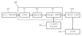
- 기판 상에 매트릭스 형태로 배치된 복수의 서브 픽셀을 포함하는 표시부;상기 표시부 외측 기판 상에서 상기 서브 픽셀의 발광 색에 대응하도록 위치하는 하나 이상의 모니터링 픽셀;상기 서브 픽셀 및 모니터링 픽셀에 전압 및 전류를 공급하는 전원공급부;외부로부터 공급된 영상 데이터를 프레임 단위로 저장하는 호스트 메모리부;상기 호스트 메모리부에 저장된 영상 데이터 프레임을 비트 단위로 불러들이고 복수의 서브필드 단위로 변환하는 데이터 조정부;상기 데이터 조정부와 연동하여 상기 호스트 메모리부에 저장된 영상 데이터 프레임을 상기 복수의 서브필드 단위로 저장하는 하나의 디스플레이 메모리부; 및상기 모니터링 픽셀에 공급된 전류를 샘플링하고 샘플링된 값을 상기 전원공급부에 전달하여 상기 서브 픽셀에 공급되는 전압을 조절하는 샘플 홀드부를 포함하되,상기 샘플 홀드부는 상기 데이터 조정부가 상기 디스플레이 메모리부에 상기 복수의 서브필드를 저장하도록 쓰기를 할 때, 상기 모니터링 픽셀에 공급된 전류를 샘플링하는 유기전계발광표시장치.
- 제1항에 있어서,상기 데이터 조정부는,상기 영상 데이터 프레임을 상기 디스플레이 메모리부에 저장할 때, 상기 서 브필드의 개수를 늘리고 늘어난 상기 서브필드의 말미 구간에 블랙 타임을 개재하는 것을 포함하는 유기전계발광표시장치.
- 제2항에 있어서,상기 모니터링 픽셀이 적색, 녹색 및 청색을 포함하고,상기 모니터링 픽셀에 전류를 공급하는 전류소스가 하나인 경우,상기 샘플 홀드부는, 상기 적색, 녹색 및 청색 모니터링 픽셀을 각각 구분하여 샘플링하는 유기전계발광표시장치.
- 제2항에 있어서,상기 모니터링 픽셀이 적색, 녹색 및 청색을 포함하고,상기 모니터링 픽셀에 전류를 공급하는 전류소스가 상기 모니터링 픽셀에 대응하도록 세 개인 경우,상기 샘플 홀드부는, 상기 적색, 녹색 및 청색 모니터링 픽셀 모두 동일한 구간에 샘플링하는 유기전계발광표시장치.
- 제3항 또는 4항에 있어서,상기 샘플 홀드부는, 상기 서브필드의 말미 구간에 개재된 블랙 타임 구간이 상기 표시부에 공급될 때, 상기 모니터링 픽셀을 샘플링하는 유기전계발광표시장치.
- 제1항에 있어서,상기 데이터 조정부가 상기 디스플레이 메모리부에 상기 복수의 서브필드를 저장하도록 쓰기를 할 때, 상기 표시부는 비 표시 상태인 유기전계발광표시장치.
- 제2항에 있어서,상기 데이터 조정부는 순람표(Look-up Table)를 포함하며,상기 순람표는 상기 영상 데이터 프레임에 상응하는 데이터를 토대로 상기 서브필드의 개수를 늘리고 늘어난 상기 서브필드의 말미 구간에 블랙 타임을 개재하는 유기전계발광표시장치.
- 제2항에 있어서,상기 데이터 조정부는 서브필드 배열부를 포함하며,상기 서브필드 배열부는 블랙 타임이 개재된 상기 서브필드를 상기 디스플레이 메모리부에 저장할 수 있도록 배열하는 유기전계발광표시장치.
- 제2항에 있어서,상기 블랙 타임이 개재된 구간은,하나의 서브필드의 총 구간의 0 초과 30% 이하의 크기로 설정되는 유기전계발광표시장치.
- 제1항에 있어서,상기 샘플 홀드부는,둘 이상의 스위치부와, 하나 이상의 커패시터와, 하나 이상의 증폭기를 포함하는 유기전계발광표시장치.
- 제1항에 있어서,상기 서브필드는,LSB(Least Significant Bit)와 MSB(Most Significant Bit)의 위치가 일부이상 혼합되도록 배열된 유기전계발광표시장치.
- 제1항에 있어서,상기 서브 픽셀은,하나 이상의 커패시터 및 트랜지스터를 포함하는 트랜지스터 어레이에 유기 발광다이오드가 연결된 유기전계발광표시장치.
Priority Applications (2)
| Application Number | Priority Date | Filing Date | Title |
|---|---|---|---|
| KR1020070049389A KR101365856B1 (ko) | 2007-05-21 | 2007-05-21 | 유기전계발광표시장치 |
| US11/952,752 US8421718B2 (en) | 2007-05-21 | 2007-12-07 | Organic light emitting device |
Applications Claiming Priority (1)
| Application Number | Priority Date | Filing Date | Title |
|---|---|---|---|
| KR1020070049389A KR101365856B1 (ko) | 2007-05-21 | 2007-05-21 | 유기전계발광표시장치 |
Publications (2)
| Publication Number | Publication Date |
|---|---|
| KR20080102670A KR20080102670A (ko) | 2008-11-26 |
| KR101365856B1 true KR101365856B1 (ko) | 2014-02-21 |
Family
ID=40288313
Family Applications (1)
| Application Number | Title | Priority Date | Filing Date |
|---|---|---|---|
| KR1020070049389A Active KR101365856B1 (ko) | 2007-05-21 | 2007-05-21 | 유기전계발광표시장치 |
Country Status (1)
| Country | Link |
|---|---|
| KR (1) | KR101365856B1 (ko) |
Cited By (2)
| Publication number | Priority date | Publication date | Assignee | Title |
|---|---|---|---|---|
| KR20150139101A (ko) * | 2014-06-02 | 2015-12-11 | 삼성디스플레이 주식회사 | 픽셀 데이터 모니터링 장치 및 방법과 이를 채용한 표시 시스템 |
| US10147383B2 (en) | 2015-04-07 | 2018-12-04 | Samsung Electronics Co., Ltd. | Display device using power sync signal to conserve power and operating method for the same |
Citations (4)
| Publication number | Priority date | Publication date | Assignee | Title |
|---|---|---|---|---|
| JP2003280600A (ja) | 2002-03-20 | 2003-10-02 | Hitachi Ltd | 表示装置およびその駆動方法 |
| US20030214521A1 (en) | 2002-05-15 | 2003-11-20 | Semiconductor Energy Laboratory Co., Ltd. | Passive matrix light emitting device |
| US20050168490A1 (en) | 2002-04-26 | 2005-08-04 | Toshiba Matsushita Display Technology Co., Ltd. | Drive method of el display apparatus |
| KR20060029062A (ko) * | 2004-09-30 | 2006-04-04 | 엘지.필립스 엘시디 주식회사 | 유기발광소자 표시장치 |
-
2007
- 2007-05-21 KR KR1020070049389A patent/KR101365856B1/ko active Active
Patent Citations (4)
| Publication number | Priority date | Publication date | Assignee | Title |
|---|---|---|---|---|
| JP2003280600A (ja) | 2002-03-20 | 2003-10-02 | Hitachi Ltd | 表示装置およびその駆動方法 |
| US20050168490A1 (en) | 2002-04-26 | 2005-08-04 | Toshiba Matsushita Display Technology Co., Ltd. | Drive method of el display apparatus |
| US20030214521A1 (en) | 2002-05-15 | 2003-11-20 | Semiconductor Energy Laboratory Co., Ltd. | Passive matrix light emitting device |
| KR20060029062A (ko) * | 2004-09-30 | 2006-04-04 | 엘지.필립스 엘시디 주식회사 | 유기발광소자 표시장치 |
Cited By (3)
| Publication number | Priority date | Publication date | Assignee | Title |
|---|---|---|---|---|
| KR20150139101A (ko) * | 2014-06-02 | 2015-12-11 | 삼성디스플레이 주식회사 | 픽셀 데이터 모니터링 장치 및 방법과 이를 채용한 표시 시스템 |
| KR102133225B1 (ko) | 2014-06-02 | 2020-07-14 | 삼성디스플레이 주식회사 | 픽셀 데이터 모니터링 장치 및 방법과 이를 채용한 표시 시스템 |
| US10147383B2 (en) | 2015-04-07 | 2018-12-04 | Samsung Electronics Co., Ltd. | Display device using power sync signal to conserve power and operating method for the same |
Also Published As
| Publication number | Publication date |
|---|---|
| KR20080102670A (ko) | 2008-11-26 |
Similar Documents
| Publication | Publication Date | Title |
|---|---|---|
| US9691329B2 (en) | Organic light emitting display device configured to measure deterioration information, and driving method thereof | |
| US8797314B2 (en) | Pixel circuit and organic electro-luminescent display apparatus | |
| JP4980977B2 (ja) | 有機電界発光表示装置及びその駆動方法 | |
| JP5080765B2 (ja) | データ駆動回路、それを備えた平板表示装置、そのデータ駆動方法 | |
| JP4589614B2 (ja) | 画像表示装置 | |
| US8421718B2 (en) | Organic light emitting device | |
| EP1821282A2 (en) | Display device and driving method thereof | |
| KR100896046B1 (ko) | 유기전계발광표시장치 | |
| JP4295247B2 (ja) | 有機電界発光表示装置及び逆多重化装置 | |
| KR20080060886A (ko) | 유기전계발광소자 디스플레이 구동방법 및 이의 구동장치 | |
| US8154482B2 (en) | Organic light emitting display and method for driving the same | |
| JP4880297B2 (ja) | 有機発光ダイオードの駆動システム及び駆動方法 | |
| KR20070101023A (ko) | 표시 장치 및 그의 구동 방법 | |
| KR101365856B1 (ko) | 유기전계발광표시장치 | |
| KR20140075040A (ko) | 유기 발광 표시 장치 및 그의 구동 방법 | |
| KR102729891B1 (ko) | 전계 발광 표시장치와 그 구동방법 | |
| KR101365863B1 (ko) | 유기전계발광표시장치 | |
| US20090051710A1 (en) | Display Method in an Active Matrix Display Device | |
| KR100894196B1 (ko) | 유기 전계 발광 표시 장치 | |
| KR101495358B1 (ko) | 유기전계발광표시장치와 이의 구동방법 | |
| US20100085388A1 (en) | Active matrix display device | |
| KR102138592B1 (ko) | 유기 발광 표시 장치 및 유기 발광 표시 장치의 구동 방법 | |
| KR20110068164A (ko) | 유기전계발광표시장치 | |
| KR101380500B1 (ko) | 유기전계발광표시장치 | |
| KR101361876B1 (ko) | 전계발광표시장치 및 이의 구동방법 |
Legal Events
| Date | Code | Title | Description |
|---|---|---|---|
| PA0109 | Patent application |
Patent event code: PA01091R01D Comment text: Patent Application Patent event date: 20070521 |
|
| N231 | Notification of change of applicant | ||
| PN2301 | Change of applicant |
Patent event date: 20080124 Comment text: Notification of Change of Applicant Patent event code: PN23011R01D |
|
| PG1501 | Laying open of application | ||
| A201 | Request for examination | ||
| PA0201 | Request for examination |
Patent event code: PA02012R01D Patent event date: 20120507 Comment text: Request for Examination of Application Patent event code: PA02011R01I Patent event date: 20070521 Comment text: Patent Application |
|
| E902 | Notification of reason for refusal | ||
| PE0902 | Notice of grounds for rejection |
Comment text: Notification of reason for refusal Patent event date: 20130814 Patent event code: PE09021S01D |
|
| E701 | Decision to grant or registration of patent right | ||
| PE0701 | Decision of registration |
Patent event code: PE07011S01D Comment text: Decision to Grant Registration Patent event date: 20131230 |
|
| GRNT | Written decision to grant | ||
| PR0701 | Registration of establishment |
Comment text: Registration of Establishment Patent event date: 20140214 Patent event code: PR07011E01D |
|
| PR1002 | Payment of registration fee |
Payment date: 20140214 End annual number: 3 Start annual number: 1 |
|
| PG1601 | Publication of registration | ||
| FPAY | Annual fee payment |
Payment date: 20170116 Year of fee payment: 4 |
|
| PR1001 | Payment of annual fee |
Payment date: 20170116 Start annual number: 4 End annual number: 4 |
|
| FPAY | Annual fee payment |
Payment date: 20190114 Year of fee payment: 6 |
|
| PR1001 | Payment of annual fee |
Payment date: 20190114 Start annual number: 6 End annual number: 6 |
|
| FPAY | Annual fee payment |
Payment date: 20200116 Year of fee payment: 7 |
|
| PR1001 | Payment of annual fee |
Payment date: 20200116 Start annual number: 7 End annual number: 7 |
|
| PR1001 | Payment of annual fee |
Payment date: 20210118 Start annual number: 8 End annual number: 8 |
|
| PR1001 | Payment of annual fee |
Payment date: 20220120 Start annual number: 9 End annual number: 9 |
|
| PR1001 | Payment of annual fee |
Payment date: 20230116 Start annual number: 10 End annual number: 10 |
|
| PR1001 | Payment of annual fee |
Payment date: 20240115 Start annual number: 11 End annual number: 11 |
|
| PR1001 | Payment of annual fee |
Payment date: 20250115 Start annual number: 12 End annual number: 12 |