KR101365856B1 - Organic Light Emitting Display - Google Patents
Organic Light Emitting Display Download PDFInfo
- Publication number
- KR101365856B1 KR101365856B1 KR1020070049389A KR20070049389A KR101365856B1 KR 101365856 B1 KR101365856 B1 KR 101365856B1 KR 1020070049389 A KR1020070049389 A KR 1020070049389A KR 20070049389 A KR20070049389 A KR 20070049389A KR 101365856 B1 KR101365856 B1 KR 101365856B1
- Authority
- KR
- South Korea
- Prior art keywords
- unit
- display
- subfields
- subfield
- monitoring
- Prior art date
Links
- 238000012544 monitoring process Methods 0.000 claims abstract description 78
- 230000015654 memory Effects 0.000 claims abstract description 66
- 238000005070 sampling Methods 0.000 claims abstract description 32
- 239000011159 matrix material Substances 0.000 claims abstract description 9
- 239000000758 substrate Substances 0.000 claims abstract description 9
- 238000000034 method Methods 0.000 claims description 27
- 239000003990 capacitor Substances 0.000 claims description 12
- 239000003086 colorant Substances 0.000 abstract description 2
- 238000010586 diagram Methods 0.000 description 22
- 101100214488 Solanum lycopersicum TFT2 gene Proteins 0.000 description 6
- 101100489584 Solanum lycopersicum TFT1 gene Proteins 0.000 description 3
- 238000006243 chemical reaction Methods 0.000 description 2
- 230000000694 effects Effects 0.000 description 2
- 238000002347 injection Methods 0.000 description 2
- 239000007924 injection Substances 0.000 description 2
- 238000007796 conventional method Methods 0.000 description 1
- 230000006866 deterioration Effects 0.000 description 1
- 238000007599 discharging Methods 0.000 description 1
- 230000005525 hole transport Effects 0.000 description 1
- 239000011147 inorganic material Substances 0.000 description 1
- 229910010272 inorganic material Inorganic materials 0.000 description 1
- 239000000203 mixture Substances 0.000 description 1
- 238000012986 modification Methods 0.000 description 1
- 230000004048 modification Effects 0.000 description 1
- 230000003287 optical effect Effects 0.000 description 1
- 239000011368 organic material Substances 0.000 description 1
- 230000008707 rearrangement Effects 0.000 description 1
- 238000012546 transfer Methods 0.000 description 1
Images


Classifications
-
- G—PHYSICS
- G09—EDUCATION; CRYPTOGRAPHY; DISPLAY; ADVERTISING; SEALS
- G09G—ARRANGEMENTS OR CIRCUITS FOR CONTROL OF INDICATING DEVICES USING STATIC MEANS TO PRESENT VARIABLE INFORMATION
- G09G3/00—Control arrangements or circuits, of interest only in connection with visual indicators other than cathode-ray tubes
- G09G3/20—Control arrangements or circuits, of interest only in connection with visual indicators other than cathode-ray tubes for presentation of an assembly of a number of characters, e.g. a page, by composing the assembly by combination of individual elements arranged in a matrix no fixed position being assigned to or needed to be assigned to the individual characters or partial characters
- G09G3/2007—Display of intermediate tones
- G09G3/2074—Display of intermediate tones using sub-pixels
-
- G—PHYSICS
- G09—EDUCATION; CRYPTOGRAPHY; DISPLAY; ADVERTISING; SEALS
- G09G—ARRANGEMENTS OR CIRCUITS FOR CONTROL OF INDICATING DEVICES USING STATIC MEANS TO PRESENT VARIABLE INFORMATION
- G09G3/00—Control arrangements or circuits, of interest only in connection with visual indicators other than cathode-ray tubes
- G09G3/20—Control arrangements or circuits, of interest only in connection with visual indicators other than cathode-ray tubes for presentation of an assembly of a number of characters, e.g. a page, by composing the assembly by combination of individual elements arranged in a matrix no fixed position being assigned to or needed to be assigned to the individual characters or partial characters
- G09G3/22—Control arrangements or circuits, of interest only in connection with visual indicators other than cathode-ray tubes for presentation of an assembly of a number of characters, e.g. a page, by composing the assembly by combination of individual elements arranged in a matrix no fixed position being assigned to or needed to be assigned to the individual characters or partial characters using controlled light sources
- G09G3/30—Control arrangements or circuits, of interest only in connection with visual indicators other than cathode-ray tubes for presentation of an assembly of a number of characters, e.g. a page, by composing the assembly by combination of individual elements arranged in a matrix no fixed position being assigned to or needed to be assigned to the individual characters or partial characters using controlled light sources using electroluminescent panels
- G09G3/32—Control arrangements or circuits, of interest only in connection with visual indicators other than cathode-ray tubes for presentation of an assembly of a number of characters, e.g. a page, by composing the assembly by combination of individual elements arranged in a matrix no fixed position being assigned to or needed to be assigned to the individual characters or partial characters using controlled light sources using electroluminescent panels semiconductive, e.g. using light-emitting diodes [LED]
- G09G3/3208—Control arrangements or circuits, of interest only in connection with visual indicators other than cathode-ray tubes for presentation of an assembly of a number of characters, e.g. a page, by composing the assembly by combination of individual elements arranged in a matrix no fixed position being assigned to or needed to be assigned to the individual characters or partial characters using controlled light sources using electroluminescent panels semiconductive, e.g. using light-emitting diodes [LED] organic, e.g. using organic light-emitting diodes [OLED]
- G09G3/3225—Control arrangements or circuits, of interest only in connection with visual indicators other than cathode-ray tubes for presentation of an assembly of a number of characters, e.g. a page, by composing the assembly by combination of individual elements arranged in a matrix no fixed position being assigned to or needed to be assigned to the individual characters or partial characters using controlled light sources using electroluminescent panels semiconductive, e.g. using light-emitting diodes [LED] organic, e.g. using organic light-emitting diodes [OLED] using an active matrix
- G09G3/3258—Control arrangements or circuits, of interest only in connection with visual indicators other than cathode-ray tubes for presentation of an assembly of a number of characters, e.g. a page, by composing the assembly by combination of individual elements arranged in a matrix no fixed position being assigned to or needed to be assigned to the individual characters or partial characters using controlled light sources using electroluminescent panels semiconductive, e.g. using light-emitting diodes [LED] organic, e.g. using organic light-emitting diodes [OLED] using an active matrix with pixel circuitry controlling the voltage across the light-emitting element
-
- G—PHYSICS
- G09—EDUCATION; CRYPTOGRAPHY; DISPLAY; ADVERTISING; SEALS
- G09G—ARRANGEMENTS OR CIRCUITS FOR CONTROL OF INDICATING DEVICES USING STATIC MEANS TO PRESENT VARIABLE INFORMATION
- G09G5/00—Control arrangements or circuits for visual indicators common to cathode-ray tube indicators and other visual indicators
- G09G5/36—Control arrangements or circuits for visual indicators common to cathode-ray tube indicators and other visual indicators characterised by the display of a graphic pattern, e.g. using an all-points-addressable [APA] memory
- G09G5/39—Control of the bit-mapped memory
-
- G—PHYSICS
- G09—EDUCATION; CRYPTOGRAPHY; DISPLAY; ADVERTISING; SEALS
- G09G—ARRANGEMENTS OR CIRCUITS FOR CONTROL OF INDICATING DEVICES USING STATIC MEANS TO PRESENT VARIABLE INFORMATION
- G09G2300/00—Aspects of the constitution of display devices
- G09G2300/04—Structural and physical details of display devices
- G09G2300/0439—Pixel structures
- G09G2300/0452—Details of colour pixel setup, e.g. pixel composed of a red, a blue and two green components
-
- G—PHYSICS
- G09—EDUCATION; CRYPTOGRAPHY; DISPLAY; ADVERTISING; SEALS
- G09G—ARRANGEMENTS OR CIRCUITS FOR CONTROL OF INDICATING DEVICES USING STATIC MEANS TO PRESENT VARIABLE INFORMATION
- G09G2310/00—Command of the display device
- G09G2310/02—Addressing, scanning or driving the display screen or processing steps related thereto
- G09G2310/0264—Details of driving circuits
- G09G2310/0291—Details of output amplifiers or buffers arranged for use in a driving circuit
-
- G—PHYSICS
- G09—EDUCATION; CRYPTOGRAPHY; DISPLAY; ADVERTISING; SEALS
- G09G—ARRANGEMENTS OR CIRCUITS FOR CONTROL OF INDICATING DEVICES USING STATIC MEANS TO PRESENT VARIABLE INFORMATION
- G09G2320/00—Control of display operating conditions
- G09G2320/02—Improving the quality of display appearance
- G09G2320/029—Improving the quality of display appearance by monitoring one or more pixels in the display panel, e.g. by monitoring a fixed reference pixel
-
- G—PHYSICS
- G09—EDUCATION; CRYPTOGRAPHY; DISPLAY; ADVERTISING; SEALS
- G09G—ARRANGEMENTS OR CIRCUITS FOR CONTROL OF INDICATING DEVICES USING STATIC MEANS TO PRESENT VARIABLE INFORMATION
- G09G2360/00—Aspects of the architecture of display systems
- G09G2360/12—Frame memory handling
Landscapes
- Engineering & Computer Science (AREA)
- Physics & Mathematics (AREA)
- Computer Hardware Design (AREA)
- General Physics & Mathematics (AREA)
- Theoretical Computer Science (AREA)
- Control Of El Displays (AREA)
- Electroluminescent Light Sources (AREA)
- Control Of Indicators Other Than Cathode Ray Tubes (AREA)
Abstract
본 발명은, 기판 상에 매트릭스 형태로 배치된 복수의 서브 픽셀을 포함하는 표시부; 표시부 외측 기판 상에서 서브 픽셀의 발광 색에 대응하도록 위치하는 하나 이상의 모니터링 픽셀; 서브 픽셀 및 모니터링 픽셀에 전압 및 전류를 공급하는 전원공급부; 호스트 메모리부에 저장된 영상 데이터 프레임을 비트 단위로 불러들이고 복수의 서브필드 단위로 변환하는 데이터 조정부; 데이터 조정부와 연동하여 호스트 메모리부에 저장된 영상 데이터 프레임을 복수의 서브필드 단위로 저장하는 하나의 디스플레이 메모리부; 및 모니터링 픽셀에 공급된 전류를 샘플링하고 샘플링된 값을 전원공급부에 전달하여 서브 픽셀에 공급되는 전압을 조절하는 샘플 홀드부를 포함하되, 샘플 홀드부는 데이터 조정부가 디스플레이 메모리부에 복수의 서브필드를 저장하도록 쓰기를 할 때, 모니터링 픽셀에 공급된 전류를 샘플링하는 유기전계발광표시장치를 제공한다.The present invention provides a display device including a plurality of sub pixels arranged in a matrix form on a substrate; One or more monitoring pixels positioned on the display outer substrate to correspond to emission colors of the sub pixels; A power supply unit supplying a voltage and a current to the sub pixel and the monitoring pixel; A data adjusting unit which reads the image data frame stored in the host memory unit in bit units and converts the image data frame into a plurality of subfield units; A display memory unit which stores the image data frame stored in the host memory unit in a plurality of subfields in association with the data adjusting unit; And a sample hold unit for sampling the current supplied to the monitoring pixel and transferring the sampled value to the power supply to adjust the voltage supplied to the sub pixel, wherein the sample hold unit stores the plurality of subfields in the display memory unit. An organic light emitting display device for sampling a current supplied to a monitoring pixel is provided.
유기전계발광표시장치, 샘플 홀드부, 블랙 타임 OLED display, sample holding part, black time
Description
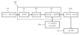
도 1은 유기전계발광표시장치의 개략적인 회로 구성도.1 is a schematic circuit diagram of an organic light emitting display device.
도 2는 도 1에 배치된 서브 픽셀의 회로 구성 예시도.FIG. 2 is an exemplary circuit diagram of a subpixel of FIG. 1. FIG.
도 3은 도 1에 도시된 데이터 조정부의 구성 예시도.3 is an exemplary configuration diagram of a data adjusting unit shown in FIG. 1.
도 4는 블랙 타임이 개재된 서브필드의 예시도.4 is an exemplary diagram of a subfield in which black time is interposed.
도 5는 복수의 서브필드 단위로 변환된 데이터 프레임 예시도.5 illustrates an example of a data frame converted in units of a plurality of subfields.
도 6은 샘플 홀드부의 블록도.6 is a block diagram of a sample hold section.
도 7은 디스플레이 메모리부 쓰기 과정과 연계한 샘플 홀드부의 샘플링 동작에 따른 구동파형의 일 예시도.7 is a diagram illustrating a driving waveform according to a sampling operation of a sample hold unit associated with a display memory unit write process;
도 8은 디스플레이 메모리부 쓰기 과정과 연계한 샘플 홀드부의 샘플링 동작에 따른 구동파형의 다른 예시도.8 is another exemplary diagram of a driving waveform according to a sampling operation of a sample hold unit associated with a display memory unit writing process;
도 9는 복수의 서브필드에 개재된 블랙 타임과 연계한 샘플 홀드부의 샘플링 동작에 따른 구동파형의 일 예시도.9 is an exemplary diagram of a driving waveform according to a sampling operation of a sample hold unit associated with black time interposed in a plurality of subfields.
도 10은 복수의 서브필드에 개재된 블랙 타임과 연계한 샘플 홀드부의 샘플링 동작에 따른 구동파형의 다른 예시도.10 is another exemplary diagram of a driving waveform according to a sampling operation of a sample hold unit associated with black time interposed in a plurality of subfields.
<도면의 주요 부분에 관한 부호의 설명>DESCRIPTION OF THE REFERENCE NUMERALS
110: 표시부 115: 서브 픽셀110: display unit 115: sub pixel
120: 모니터링 픽셀 140: 호스트 메모리부120: monitoring pixel 140: host memory portion
150: 데이터 조정부 160: 디스플레이 메모리부150: data adjustment unit 160: display memory unit
170: 제어부 180: 전원공급부170: control unit 180: power supply unit
190: 샘플 홀드부190: sample holding part
본 발명은 유기전계발광표시장치에 관한 것이다.The present invention relates to an organic light emitting display.
유기전계발광표시장치에 사용되는 유기전계발광소자는 두 개의 전극 사이에 발광층이 형성된 자발광소자였다.An organic electroluminescent device used in an organic electroluminescent display device is a self-luminous device in which a light emitting layer is formed between two electrodes.
또한, 유기전계발광소자는 빛이 방출되는 방향에 따라 전면발광(Top-Emission) 방식과 배면발광(Bottom-Emission) 방식이 있고, 구동방식에 따라 수동매트릭스형(Passive Matrix)과 능동매트릭스형(Active Matrix)으로 나누어져 있다.The organic electroluminescent device has a top emission mode and a bottom emission mode depending on a direction in which light is emitted and a passive matrix type and an active matrix type Active Matrix).
이러한 유기전계발광소자 중 능동 매트릭스형을 이용한 유기전계발광표시장치는 표시부에 매트릭스 형태로 배치된 복수의 서브 픽셀들에 스캔 신호 및 데이터 신호가 공급되면, 서브 픽셀 내부에 위치하는 트랜지스터, 커패시터 및 유기 발광다이오드가 구동하게 되어 영상을 표시할 수 있게 된다.Among the organic light emitting display devices, an organic light emitting display device using an active matrix type includes a transistor, a capacitor, and an organic light source positioned inside a subpixel when a scan signal and a data signal are supplied to a plurality of subpixels arranged in a matrix form on a display unit. The light emitting diode is driven to display an image.
종래 유기전계발광표시장치는 패널의 외부에 위치하는 장치들로부터 데이터 및 스캔 신호 등을 공급받았다. 여기서, 외부로부터 공급된 영상 데이터는 호스트 메모리에 저장되고 호스트 메모리에 저장된 데이터는 화질 튜닝단계 등을 거친 후 프레임 단위로 배열되어 표시부에 공급되었다.Conventional organic light emitting display devices receive data and scan signals from devices positioned outside the panel. Here, the image data supplied from the outside is stored in the host memory, and the data stored in the host memory is arranged in units of frames after the image quality tuning step and supplied to the display unit.
한편, 트랜지스터, 커패시터 및 유기 발광다이오드 등의 소자들에 열화가 발생하는 문제를 고려하여 표시부의 외측 기판 상에 모니터링 픽셀들을 구비하고 표시부 내에 위치한 서브 픽셀들에 공급되는 전원을 샘플링하고 샘플링된 값에 따라 서브 픽셀에 공급되는 전원을 조절하여 서브 픽셀의 변화된 특성을 보상하도록 하였다.On the other hand, in consideration of the deterioration of devices such as transistors, capacitors, and organic light emitting diodes, the monitoring pixels are provided on the outer substrate of the display unit, and the power supplied to the subpixels located in the display unit is sampled and Accordingly, the power supplied to the subpixel is adjusted to compensate for the changed characteristic of the subpixel.
여기서, 모니터링 픽셀들에 공급되는 전원을 샘플링하는 샘플 홀드부의 경우, 디스플레이 메모리부의 쓰기 또는 읽기 과정이나 서브 픽셀의 발광구간 또는 비 발광구간 등 상호 연동하는 장치 간의 구동조건을 고려하는 것이 중요하다.Here, in the case of the sample holding part sampling the power supplied to the monitoring pixels, it is important to consider driving conditions between devices that interoperate with each other, such as a writing or reading process of the display memory part or a light emitting period or a non-light emitting period of the subpixel.
따라서, 이와 같이 모니터링 픽셀과 샘플 홀드부를 이용하여 서브 픽셀의 변화된 특성을 보상하기 위해서는 앞서 설명한 여러 가지 조건들을 고려하여 샘플링의 효율성과 정확성 등을 높일 수 있는 안이 마련되어야 할 것이다.Accordingly, in order to compensate for the changed characteristics of the subpixel using the monitoring pixel and the sample holding unit, a scheme for improving the efficiency and accuracy of sampling in consideration of various conditions described above should be prepared.
상술한 문제점을 해결하기 위한 본 발명의 목적은, 서브필드 단위 구동시 요구되는 디스플레이 메모리 개수를 줄이고, 모니터링 픽셀의 샘플링 효율성과 정확성을 높일 수 있는 유기전계발광표시장치를 제공하는 것이다.SUMMARY OF THE INVENTION An object of the present invention is to provide an organic light emitting display device capable of reducing the number of display memories required for subfield unit driving and increasing the sampling efficiency and accuracy of monitoring pixels.
상술한 과제를 해결하기 위한 본 발명은, 기판 상에 매트릭스 형태로 배치된 복수의 서브 픽셀을 포함하는 표시부; 표시부 외측 기판 상에서 서브 픽셀의 발광 색에 대응하도록 위치하는 하나 이상의 모니터링 픽셀; 서브 픽셀 및 모니터링 픽 셀에 전압 및 전류를 공급하는 전원공급부; 호스트 메모리부에 저장된 영상 데이터 프레임을 비트 단위로 불러들이고 복수의 서브필드 단위로 배열하는 데이터 조정부; 데이터 조정부와 연동하여 호스트 메모리부에 저장된 영상 데이터 프레임을 복수의 서브필드 단위로 저장하는 하나의 디스플레이 메모리부; 및 모니터링 픽셀에 공급된 전류를 샘플링하고 샘플링된 값을 전원공급부에 전달하여 서브 픽셀에 공급되는 전압을 조절하는 샘플 홀드부를 포함하되, 샘플 홀드부는 데이터 조정부가 디스플레이 메모리부에 복수의 서브필드를 저장하도록 쓰기를 할 때, 모니터링 픽셀에 공급된 전류를 샘플링하는 유기전계발광표시장치를 제공한다.The present invention for solving the above problems, the display unit including a plurality of sub-pixels arranged in a matrix form on the substrate; One or more monitoring pixels positioned on the display outer substrate to correspond to emission colors of the sub pixels; A power supply unit supplying a voltage and a current to the subpixel and the monitoring pixel; A data adjusting unit for reading image data frames stored in the host memory unit in units of bits and arranging the units in a plurality of subfields; A display memory unit which stores the image data frame stored in the host memory unit in a plurality of subfields in association with the data adjusting unit; And a sample hold unit for sampling the current supplied to the monitoring pixel and transferring the sampled value to the power supply to adjust the voltage supplied to the sub pixel, wherein the sample hold unit stores the plurality of subfields in the display memory unit. An organic light emitting display device for sampling a current supplied to a monitoring pixel is provided.
데이터 조정부는, 영상 데이터 프레임을 디스플레이 메모리부에 저장할 때, 서브필드의 개수를 늘리고 늘어난 서브필드의 말미 구간에 블랙 타임을 개재하는 것을 포함할 수 있다.When the image data frame is stored in the display memory unit, the data adjusting unit may include increasing the number of subfields and interposing black time in the end section of the increased subfields.
모니터링 픽셀이 적색, 녹색 및 청색을 포함하고, 모니터링 픽셀에 전류를 공급하는 전류소스가 하나인 경우, 샘플 홀드부는, 적색, 녹색 및 청색 모니터링 픽셀을 각각 구분하여 샘플링할 수 있다.When the monitoring pixel includes red, green, and blue, and there is one current source for supplying current to the monitoring pixel, the sample holding unit may separately sample the red, green, and blue monitoring pixels.
모니터링 픽셀이 적색, 녹색 및 청색을 포함하고, 모니터링 픽셀에 전류를 공급하는 전류소스가 모니터링 픽셀에 대응하도록 세 개인 경우, 샘플 홀드부는, 적색, 녹색 및 청색 모니터링 픽셀 모두 동일한 구간에 샘플링할 수 있다.When the monitoring pixel includes red, green, and blue, and three current sources supplying current to the monitoring pixel correspond to the monitoring pixel, the sample holding unit may sample all of the red, green, and blue monitoring pixels in the same interval. .
샘플 홀드부는, 서브필드의 말미 구간에 개재된 블랙 타임 구간이 상기 표시부에 공급될 때, 모니터링 픽셀을 샘플링할 수 있다.The sample hold unit may sample the monitoring pixel when the black time interval interposed in the end section of the subfield is supplied to the display unit.
데이터 조정부가 디스플레이 메모리부에 복수의 서브필드를 저장하도록 쓰기 를 할 때, 표시부는 비 표시 상태일 수 있다.When the data controller writes to store the plurality of subfields in the display memory unit, the display unit may be in a non-display state.
데이터 조정부는 순람표(Look-up Table)를 포함하며, 순람표는 영상 데이터 프레임에 상응하는 데이터를 토대로 서브필드의 개수를 늘리고 늘어난 서브필드의 말미 구간에 블랙 타임을 개재할 수 있다.The data adjusting unit includes a look-up table, and the look-up table may increase the number of subfields based on data corresponding to the image data frame and interpose black time in the end section of the increased subfield.
데이터 조정부는 서브필드 배열부를 포함하며, 서브필드 배열부는 블랙 타임이 개재된 서브필드를 디스플레이 메모리부에 저장할 수 있도록 배열할 수 있다.The data adjusting unit may include a subfield arranging unit, and the subfield arranging unit may arrange the subfield including the black time so as to be stored in the display memory unit.
블랙 타임이 개재된 구간은, 하나의 서브필드의 총 구간의 0 초과 30% 이하의 크기로 설정될 수 있다.An interval in which black time is interposed may be set to a size greater than 0 and less than 30% of the total interval of one subfield.
샘플 홀드부는, 둘 이상의 스위치부와, 하나 이상의 커패시터와, 하나 이상의 증폭기를 포함할 수 있다.The sample hold unit may include two or more switch units, one or more capacitors, and one or more amplifiers.
서브필드는, LSB(Least Significant Bit)와 MSB(Most Significant Bit)의 위치가 일부이상 혼합되도록 배열될 수 있다.The subfields may be arranged such that the positions of the least significant bit (LSB) and the most significant bit (MSB) are mixed at least partially.
서브 픽셀은, 하나 이상의 커패시터 및 트랜지스터를 포함하는 트랜지스터 어레이에 유기 발광다이오드가 연결된 것 일 수 있다.The subpixel may be an organic light emitting diode connected to a transistor array including one or more capacitors and transistors.
<일 실시예><Example 1>
도 1은 유기전계발광표시장치의 개략적인 회로 구성도이다.1 is a schematic circuit diagram of an organic light emitting display device.
도 1을 참조하면, 본 발명의 일 실시예에 따른 유기전계발광표시장치는 기판 상에 매트릭스 형태로 배치된 복수의 서브 픽셀(115)을 포함하는 표시부(110)인 패널을 포함한다. 서브 픽셀(115)은 적색, 녹색 및 청색을 발광하는 것을 일례로 설 명한다.Referring to FIG. 1, an organic light emitting display device according to an exemplary embodiment includes a panel that is a
그리고 표시부(110)의 외측 기판 상에서 서브 픽셀(115)의 발광 색에 대응하도록 위치하는 모니터링 픽셀(120)을 포함한다. 모니터링 픽셀(120)은 서브 픽셀(115)의 발광 색에 대응하도록 위치하므로, 모니터링 픽셀(120) 또한 적색, 녹색 및 청색을 발광하는 것을 일례로 설명한다.And a
그리고 서브 픽셀(115)에 전압을 공급하고 모니터링 픽셀(120)에 전류를 공급하는 전원공급부(180)를 포함한다. 전원공급부(180)는 하나의 전류소스에서 출력되는 전류를 모든 모니터링 픽셀(120)에 공급하는 방식과 모니터링 픽셀(120)에 대응하는 즉, 3개의 전류소스에서 출력되는 전류를 각각의 모니터링 픽셀(120)에 공급하는 방식 중 하나를 채택할 수 있다.The
그리고 표시부(110)에 데이터 신호 및 스캔 신호를 공급하는 구동부(130a,130b)를 포함한다. 구동부(130a,130b)는 도시된 바와 같이 표시부(110)에 데이터 신호를 공급하는 데이터 구동부(130a)와 표시부(110)에 스캔 신호를 공급하는 스캔 구동부(130b)로 구분될 수 있다.And a
그리고 외부로부터 공급된 영상 데이터를 프레임 단위로 저장하는 호스트 메모리부(140)를 포함한다. 호스트 메모리부(140)는 외부로부터 방대한 양의 영상 데이터를 저장할 수 있도록 대용량 저장장치로 구성할 수 있다.And a
그리고 호스트 메모리부(140)에 저장된 영상 데이터 프레임을 복수의 서브필드 단위로 저장하고 이를 데이터 구동부(130a)에 공급하는 하나의 디스플레이 메모리부(160)를 포함한다.And a
그리고 호스트 메모리부(140)에 저장된 영상 데이터 프레임을 비트 단위로 불러들이고 복수의 서브필드 단위로 변환하여 디스플레이 메모리부(160)에 저장하는 데이터 조정부(150)를 포함한다. 특히, 데이터 조정부(150)는 디스플레이 메모리부(160)에 서브필드 단위로 저장할 때, 서브필드의 개수를 늘리고 늘어난 서브필드의 말미 구간에 블랙 타임을 개재한다.And a
그리고 모니터링 픽셀(120)에 공급된 전류를 샘플링하고 샘플링된 값을 전원공급부(180)에 전달하여 서브 픽셀(115)에 공급되는 전압을 조절하는 샘플 홀드부(190)를 포함한다. 여기서, 샘플 홀드부(190)는 데이터 조정부(150)가 디스플레이 메모리부(160)에 복수의 서브필드를 저장하도록 쓰기를 할 때, 모니터링 픽셀(120)에 공급된 전류를 샘플링한다.And a
그리고 앞서 설명한 호스트 메모리부(140), 데이터 조정부(150), 디스플레이 메모리부(160), 구동부(130a,130b), 전원공급부(180), 샘플 홀드부(190) 등에 제어신호를 공급하는 제어부(170)를 포함한다. 제어부(170)는 각각의 장치가 상호 유기적으로 연동 및 제어될 수 있도록 제어신호를 생성하여 출력한다.In addition, a controller for supplying a control signal to the
이하, 도 2를 참조하여, 도 1에 도시된 서브 픽셀(115)의 회로 구성에 대해 더욱 자세히 설명한다.Hereinafter, the circuit configuration of the
도 2는 도 1에 배치된 서브 픽셀의 회로 구성 예시도 이다.FIG. 2 is an exemplary circuit diagram of a subpixel of FIG. 1.
도 2에 도시된 서브 픽셀들의 회로 구성도는 설명의 이해를 돕기 위한 회로 구성의 예시도 일뿐 본 발명은 이에 한정되지 않음을 참조한다.The circuit diagram of the subpixels illustrated in FIG. 2 is only an example of a circuit diagram for better understanding of the description, and the present disclosure is not limited thereto.
도 2에 도시된 바와 같이 서브 픽셀은, 스캔 배선(SCAN)에 게이트가 연결되고 데이터 배선(DATA)에 제1전극이 공통으로 연결된 스위칭 트랜지스터(TFT1)를 포함한다. 또한, 스위칭 트랜지스터(TFT1)의 제2전극에 게이트가 연결되고 제1전원배선(VDD)에 제1전극이 연결된 구동 트랜지스터(TFT2)를 포함한다. 또한, 구동 트랜지스터(TFT2)의 게이트와 제1전원배선(VDD) 사이에 연결된 커패시터(C)를 포함한다. 또한, 구동 트랜지스터(TFT2)의 제2전극과 제2전원배선(GND) 사이에 연결된 유기 발광다이오드(D)를 포함한다.As illustrated in FIG. 2, the subpixel includes a switching transistor TFT1 having a gate connected to the scan line SCAN and a first electrode connected to the data line DATA in common. In addition, the driving transistor TFT2 includes a gate connected to the second electrode of the switching transistor TFT1 and a first electrode connected to the first power line VDD. In addition, the capacitor C may be connected between the gate of the driving transistor TFT2 and the first power line VDD. In addition, the organic light emitting diode D may include an organic light emitting diode D connected between the second electrode of the driving transistor TFT2 and the second power line GND.
여기서, 유기 발광다이오드(D)는 발광층이 유기물층으로 형성된 유기 발광다이오드일 수 있으나 발광층이 무기물층으로 형성된 무기 발광다이오드일 수도 있다.Here, the organic light emitting diode D may be an organic light emitting diode in which the light emitting layer is formed of an organic material layer, but may also be an inorganic light emitting diode in which the light emitting layer is formed of an inorganic material layer.
유기 발광다이오드(D)의 구조에 대한 설명을 덧붙이면, 유기 발광다이오드(D)는 정공주입층(HIL), 정공수송층(HTL), 전자수송층(ETL) 및 전자주입층(EIL)과 같은 공통막 사이에 유기 발광층(EML)이 개재된 것을 포함한다. 일반적으로, 공통막은 애노드 전극이 되는 구동 트랜지스터(TFT2)의 제1전극(화소전극)과 캐소드 전극 사이에 선택적으로 형성된다.In addition to the description of the structure of the organic light emitting diode (D), the organic light emitting diode (D) is common, such as a hole injection layer (HIL), a hole transport layer (HTL), an electron transport layer (ETL) and an electron injection layer (EIL) The organic light emitting layer (EML) is interposed between the film. In general, the common film is selectively formed between the first electrode (pixel electrode) and the cathode of the driving transistor TFT2 serving as the anode electrode.
한편, 각 서브 픽셀의 전원배선은 각각 구분되도록 전원공급부에 연결되어 독립된 전압 즉, 서로 다른 전압을 공급받을 수 있다. 그리고 각 서브 픽셀에 포함된 트랜지스터들(TFT1,TFT2)은 앞서 설명한 구동부로부터 공급된 구동신호에 의해 선형(Linear)영역 또는 포화(Saturation)영역에서 구동할 수 있으나, 본 발명에서는 트랜지스터들(TFT1,TFT2)을 선형영역에서 구동하는 디지털 구동방식을 채택하는 것이 유리하다. 여기서, 디지털 구동방식이란, 트랜지스터를 단순히 턴온 또는 턴오프하는 방식을 말한다.On the other hand, the power wiring of each subpixel may be connected to a power supply so as to be distinguished from each other, and may receive an independent voltage, that is, a different voltage. The transistors TFT1 and TFT2 included in each subpixel may be driven in the linear region or the saturation region by the driving signal supplied from the driver as described above. It is advantageous to adopt a digital driving method for driving the TFT2) in the linear region. Here, the digital driving method refers to a method of simply turning on or off a transistor.
도시되어 있진 않지만, 도 1에 도시된 모니터링 픽셀의 경우, 앞서 설명한 서브 픽셀과 같은 구성으로 형성될 수 있으나 본 발명의 모니터링 픽셀은 하나의 커패시터와 유기 발광다이오드를 포함하는 단순한 구성을 채택하는 것이 유리하다.Although not shown, the monitoring pixel shown in FIG. 1 may be formed in the same configuration as the above-described subpixel, but it is advantageous that the monitoring pixel of the present invention adopts a simple configuration including one capacitor and an organic light emitting diode. Do.
이하, 도 3을 참조하여, 도 1에 도시된 데이터 조정부(150)에 대해 더욱 자세히 설명한다.Hereinafter, the
도 3은 도 1에 도시된 데이터 조정부의 구성 예시도 이다.3 is an exemplary configuration diagram of a data adjusting unit shown in FIG. 1.
도 3에 도시된 데이터 조정부의 예시도는 설명의 이해를 돕기 위한 것 일뿐 본 발명은 이에 한정되지 않음을 참조한다.Exemplary diagrams of the data adjusting unit shown in FIG. 3 are provided only for better understanding of the description, and the present invention is not limited thereto.
도 3에 도시된 바와 같이 데이터 조정부(150)는, 호스트 메모리부(140)에 저장된 영상 데이터 프레임을 비트 단위로 불러들이는 감마부(151)를 포함한다. 감마부(151)는 미리 저장된 감마 데이터 변환 시스템을 통해 입력된 적색(R), 녹색(G), 청색(B)의 영상 데이터 프레임을 유기전계발광표시장치의 화상 구현에 맞는 계조로 휘도 값을 변환시킨다.As illustrated in FIG. 3, the
한편, 감마부(151)는 이와 같이 감마 변환을 할 때, 내부에 포함된 순람표(Look-up Table)를 이용하여 입력된 영상 데이터 프레임에 상응하는 데이터를 토대로 서브필드의 개수를 늘리고 늘어난 서브필드의 말미 구간에 블랙 타임을 개재할 수 있다.On the other hand, the
도 4는 블랙 타임이 개재된 서브필드의 예시도 이다.4 is an exemplary diagram of a subfield in which black time is interposed.
설명의 이해를 돕기 위해 도 4를 함께 참조하면, 복수의 서브필드로 나뉜 하나의 영상 데이터 프레임(1 Frame)은 서브필드의 말미 구간에 블랙 타임(BT)이 개재되고 있음을 알 수 있다. 이에 대한 자세한 설명을 하기에 설명한다.Referring to FIG. 4 to help understand the description, it can be seen that one image data frame (1 frame) divided into a plurality of subfields has black time BT interposed in the end section of the subfield. Detailed description thereof will be described below.
앞서 설명한 바와 같이 감마 변환된 서브필드 단위의 데이터는 도시된 바와 같이 서브필드 단위로 변환된 이미지를 미세 조정하는 즉, 이미지 디더링 등을 수행하기 위해 하프톤부(153)를 거칠 수 있다.As described above, the data in the gamma-converted subfield unit may pass through the
데이터 조정부(150)는 서브필드 배열부(155)를 포함하는데, 서브필드 배열부(155)는 블랙 타임이 개재된 서브필드 단위의 데이터를 디스플레이 메모리부(160)에 저장할 수 있도록 배열을 수행함은 물론, 디스플레이 메모리부(160)에 저장된 서브필드 단위의 데이터를 데이터 구동부(130a)를 통해 표시부(110)에 공급할 수 있도록 재배열도 수행한다. 여기서, 서브필드 단위의 데이터를 재배열하는 과정은 데이터 구동부(130a)의 출력 요건에 따라 요구될 수 있다.The
이와 같이 배열된 서브필드 단위의 데이터는 디스플레이 메모리부(160)에 저장된 후, 데이터 구동부(130a)를 통해 표시부(110)에 공급된다. 그러면 표시부(110)는 공급받은 신호에 따른 영상을 구현할 수 있게 된다.The data in the subfield units arranged as described above are stored in the
이와 같은 과정에서 디스플레이 메모리부(160)는, 데이터 조정부(150)에 의해 호스트 메모리부(140)에 저장된 영상 데이터 프레임을 비트단위로 불러 들여 복수의 서브필드 단위로 저장하는 쓰기 단계와, 디스플레이 메모리부(160)에 저장된 서브필드를 데이터 구동부(130a)가 읽어내는 읽기 단계를 교번하게 된다. 단, 디스플레이 메모리부(160)가 복수의 서브필드를 저장하도록 쓰기를 할 때, 표시부(110)는 비 표시 상태가 된다.In this process, the
한편, 앞서 설명에서는 순람표가 감마부(151)와 연동하는 것으로 설명하였으나 이는 실시예의 일례일 뿐, 순람표는 감마부(151)와 함께 연동하지 않고 영상 데이터 프레임에 상응하도록 테이블화된 데이터를 토대로 수행가능함은 물론이다.Meanwhile, in the above description, the lookup table has been described as interlocking with the
그리고 순람표는 호스트 메모리부(140)로부터 영상 데이터 프레임을 비트 단위로 불러들일 때, 비트 단위를 늘려서 불러들인다. 즉, 종래 방식에서 영상 데이터 프레임을 6비트 단위로 불러들였다고 가정하면, 본 발명에서는 서브필드의 개수를 늘릴 수 있도록 8비트 이상으로 영상 데이터 프레임을 불러들이는 것이 유리하다.When the image data frame is read in units of bits from the
이를 서브필드의 개수를 참조하여 설명을 덧붙이면, 데이터 조정부(150)는 서브필드의 개수를 늘릴 때, 1개 이상으로 늘려 늘어난 구간에 블랙 타임을 개재하게 된다.If the description is added with reference to the number of subfields, when the number of subfields is increased, the
한편, 종래 6비트 단위로 영상 데이터 프레임을 디스플레이 메모리부(160)에 저장하는 경우, 서브필드는 16개의 서브필드로 분할하여 저장되었다. 그러나 8비트 이상으로 영상 데이터 프레임을 디스플레이 메모리부(160)에 저장하는 경우, 서브필드는 28개 이상의 서브필드로 분할하여 저장할 수 있게 된다. 이와 같이 서브필드의 개수를 늘리는 것은 블랙 타임을 개재함으로써, 차기에 디스플레이 메모리부(160)에 저장되는 서브필드와 중첩되는 현상을 저지하기 위함이다. 이는, 현재 데이터와 차기 데이터 간에 구분 영역을 두는 것과 같다.Meanwhile, when the image data frame is stored in the
참고로, 이와 같이 서브필드의 개수를 늘려서 디스플레이 메모리부(160)에 쓰거나 읽을 때는 높은 주파수를 이용하는 것이 유리하며, 비트의 수와 서브필드의 수는 설명된 것에 한정되지 않는다.For reference, it is advantageous to use a high frequency when writing or reading the
이하, 도 5를 참조하여, 데이터 조정부(150)를 통해 조정된 서브필드에 대해 더욱 자세히 설명한다.Hereinafter, the subfield adjusted through the
도 5는 복수의 서브필드 단위로 변환된 데이터 프레임 예시도 이다.5 illustrates an example of a data frame converted in units of a plurality of subfields.
도 5를 참조하면, 하나의 영상 데이터 프레임(1 Frame)은 복수의 서브필드 설명의 일례로, 28개의 서브필드(SF1..SF28)로 나뉜다고 가정한다. 이와 같이 28개로 나뉜 서브필드의 전반(SF1..SF25) 각각은 어드레스 구간과 발광구간으로 구분된다. 그리고 이들의 말미 구간(예: SF26,SF27,SF28)에는 블랙 타임(BT)이 개재된다.Referring to FIG. 5, it is assumed that one image data frame (1 frame) is divided into 28 subfields SF1..SF28 as an example of description of a plurality of subfields. As described above, each of the first half of the 28 subfields (SF1..SF25) is divided into an address section and a light emission section. In addition, black time (BT) is interposed in the last section (eg, SF26, SF27, SF28).
여기서, 도시된 영상 데이터 프레임(1 Frame)은 앞서 설명한 디스플레이 메모리부에 저장된 형태를 나타내는 것은 아니다. 다만, 설명의 이해를 돕기 위해 정형화된 형태로 나타낸 것이고, 이는 표시부에 공급될 수 있도록 배열된 형태이다.Here, the illustrated
이와 같이 복수의 서브필드 단위로 조정된 데이터 프레임은, 하나의 서브필드 내에 속하는 어드레스 구간에 스캔 신호가 공급되면, 발광할 서브 픽셀을 선택하게 되고, 선택된 서브 픽셀에 데이터 신호가 공급되면, 유기발광다이오드가 발광을 하게 된다.As described above, when a scan signal is supplied to an address section belonging to one subfield, a data frame adjusted in units of a plurality of subfields selects a subpixel to emit light, and when a data signal is supplied to the selected subpixel, organic light emission is performed. The diode will emit light.
한편, 발광구간은 각 서브필드에서의 계조 가중치를 결정하는 기간이다. 예 를 들어, 제 1 서브필드(SF1)의 계조 가중치를 20으로 설정하고, 제 2 서브필드의 계조 가중치를 21으로 설정하는 방법으로 각 서브필드의 계조 가중치가 2n (단, n=0, 1, 2, 3, 4, 5)의 비율로 증가되도록 각 서브필드의 계조 가중치를 결정할 수 있다.On the other hand, the light emission period is a period for determining the gray scale weight in each subfield. For example, the gray scale weight of each subfield is 2 n by setting the gray scale weight of the first subfield SF1 to 2 0 and the gray scale weight of the second subfield to 2 1 . The gray scale weight of each subfield may be determined to increase at a ratio of 0, 1, 2, 3, 4, and 5).
이와 같이, 각 서브필드의 발광구간에서는 계조 가중치에 따라 각 서브필드의 발광유지시간을 조절함으로써, 다양한 영상에 대한 계조를 구현할 수 있게 된다. 단, 앞서 설명한 계조 가중치는 일례일 뿐이다.As described above, in the light emitting period of each subfield, the gray scale for various images can be realized by adjusting the light emission holding time of each subfield according to the gray scale weight. However, the gray scale weight described above is just an example.
참고로, 서브필드의 최하위 비트(Least Significant Bit)는 발광시간이 짧기 때문에 발광시간을 소거할 수 있는 소거 구간이 삽입될 수도 있다. 소거 구간에는 서브 픽셀의 커패시터에 저장된 데이터 신호를 디스차지 하는 방법으로 유기발광다이오드의 발광을 중단시키게 된다.For reference, since the least significant bit of the subfield has a short emission time, an erasing section for erasing the emission time may be inserted. In the erase period, light emission of the organic light emitting diode is stopped by discharging the data signal stored in the capacitor of the subpixel.
그리고 서브필드의 말미에 개재된 블랙 타임(BT)은 어드레스 구간과 발광구간과는 달리 영상을 표현하지 않는다. 즉, 비 표시 구간 상태가 된다.The black time BT interposed at the end of the subfield does not represent an image unlike an address section and a light emission section. That is, it becomes a non-display section state.
따라서, 서브필드의 말미에 블랙 타임(BT) 구간을 개재할 때는 하나의 서브필드의 총 구간의 0 초과 30% 이하의 크기로 설정하는 것이 유리하다. 여기서, 블랙 타임(BT) 구간의 이상적인 크기는 대략 5%이상 15%이하가 될 수 있다.Therefore, when the black time (BT) section is interposed at the end of the subfield, it is advantageous to set the size to more than 0 and 30% or less of the total section of one subfield. Here, the ideal size of the black time BT period may be about 5% or more and 15% or less.
이와 같이 블랙 타임(BT)이 개재된 구간을 5% 내지 15%로 하게 되면, 디스플레이 메모리를 억세스할 때, 빠른 주파수 클록으로 읽기와, 쓰기를 수행할 수 있기 때문이다.This is because when the period in which the black time BT is interposed is set to 5% to 15%, the display memory can be read and written with a fast frequency clock when the display memory is accessed.
한편, 앞서 설명한 서브필드는 LSB와 MSB(Most Significant Bit)의 위치가 일부이상 혼합되도록 배열될 수 있다. 이는 영상 데이터 프레임(1 Frame)을 복수의 서브필드로 나눌 때, 서브필드의 발광구간이 뒤로 갈수록 길어지면서 특정 영역으로 광 중심이 쏠리는 현상을 저지하기 위해서다.Meanwhile, the above-described subfields may be arranged such that the positions of the LSB and the Most Significant Bit (MSB) are partially mixed. This is to prevent the phenomenon that the optical center is focused on a specific area when the image data frame (1 frame) is divided into a plurality of subfields, and the light emitting period of the subfields is longer toward the rear.
이와 관련된 설명을 덧붙이면, 앞서 들어온 데이터의 MSB가 길게 발광을 하게 되고, 차기에 들어오는 데이터의 LSB가 짧게 발광을 하게 되면, 시감을 떨어뜨릴 우려가 있으므로 이와 같은 현상을 고려한다면 서브필드의 배열을 다양하게 혼합되도록 위치시키는 것이 유리함을 알 수 있을 것이다.In addition to this description, if the MSB of the previously input data emits a long light and the LSB of the next incoming data emits a short light, there is a possibility that the sense of vision may be degraded. It will be appreciated that it is advantageous to locate the various mixtures.
이하, 도 6을 참조하여 샘플 홀드부에 대한 설명을 더욱 자세히 한다.Hereinafter, the description will be given in detail with reference to FIG. 6.
도 6은 샘플 홀드부의 블록도 이다.6 is a block diagram of a sample hold unit.
도 6을 참조하면, 샘플 홀드부는 전원공급부(180)가 모니터링 픽셀(120)에 전류를 공급할 때, 공급되는 전류(Im)를 전압으로 샘플링하여 전원공급부(180)에 샘플링 값을 피드백(FB) 신호로 전달한다. 그러면, 전원공급부(180)는 샘플링 값을 참조하여 서브 픽셀(115)에 공급할 전압(Vm)을 조절하게 된다.Referring to FIG. 6, when the
이와 같이 모니터링 픽셀(120)에 공급되는 전류를 전압으로 샘플링하고 샘플링된 값을 전원공급부(180)에 전달하기 위해서 샘플 홀드부는, 둘 이상의 스위치부와 하나 이상의 커패시터와 하나 이상의 증폭기를 포함할 수 있다.As such, the sample holding unit may include two or more switch units, one or more capacitors, and one or more amplifiers to sample the current supplied to the
이를 더욱 자세히 설명하면, 샘플 홀드부(190)에 포함된 둘 이상의 스위치부 중 하나는 전원공급부(180)와 모니터링 픽셀(120) 사이를 연결하는 전원배선에 위 치하여 모니터링 픽셀(120)에 전류(Im)가 공급 되도록 스위칭 동작을 하게 된다. 그리고 다른 하나는 모니터링 픽셀(120)의 전원배선에 연결되어 모니터링 픽셀(120)에 공급되는 전류(Im)을 샘플링하게 된다. 그리고 이때 샘플링된 전류(Im)은 커패시터에 전압으로 홀드되고, 홀드된 전압은 증폭기를 거쳐 전원공급부(180)에 피드백(FB) 신호로 전달된다. 그러면, 전원공급부(180)는 이를 참조하여 서브 픽셀(115)에 공급할 전압을 조절하게 된다.In more detail, one of the two or more switch units included in the
한편, 본 발명의 일 실시예에 따른 유기전계발광표시장치는 앞서 설명한 일련의 구동과정에서 샘플 홀드부는 데이터 조정부가 디스플레이 메모리부에 복수의 서브필드를 저장하도록 쓰기를 할 때, 모니터링 픽셀에 공급된 전류를 샘플링한다.On the other hand, the organic light emitting display device according to an embodiment of the present invention is supplied to the monitoring pixel when the sample holding unit writes the data adjusting unit to store the plurality of subfields in the display memory in the series of driving processes described above. Sample the current.
이하, 도 7 및 도 8을 참조하여 디스플레이 메모리부가 서브필드를 저장하도록 쓰기를 할 때, 전원공급부에 포함된 전류소스가 하나인 경우와 3개인 경우의 두 가지를 실시예로 모니터링 픽셀에 공급된 전류를 공급하는 샘플링하는 것을 설명한다.Hereinafter, referring to FIGS. 7 and 8, when a display memory unit writes to store a subfield, two types of current sources included in the power supply unit and three cases are supplied to the monitoring pixel. Sampling to supply current will be described.
도 7은 디스플레이 메모리부 쓰기 과정과 연계한 샘플 홀드부의 샘플링 동작에 따른 구동파형의 일 예시도 이다.7 is a diagram illustrating a driving waveform according to a sampling operation of a sample hold unit associated with a display memory unit writing process.
도 7의 샘플링 구동파형은 전원공급부에 포함된 전류소스가 하나인 경우를 가정한 예시도 이다.7 is an exemplary view assuming that there is only one current source included in the power supply unit.
도 7을 참조하면, 디스플레이 메모리부(MM)가 쓰기 동작을 하는 구간인 메모리 라이팅 타임(MWT)에, 샘플 홀드부는 적색 모니터링 픽셀(MR), 녹색 모니터링 픽 셀(MG) 및 청색 모니터링 픽셀(MB)을 각각 구분하여 샘플링함을 알 수 있다.Referring to FIG. 7, in the memory writing time MWT, which is a period in which the display memory unit MM writes, the sample holding unit red monitoring pixel MR, green monitoring pixel MG, and blue monitoring pixel MB. You can see that each sample separately).
통상 전원공급부에 포함된 전류소스가 하나인 경우, 하나의 전류소스는 각 모니터링 픽셀(MR,MG,MB)에 각기 다른 전류를 공급할 수 있도록 시분할 스위칭을 하거나 전류 분배기 등을 이용해야 하기 때문에 이와 같이 구분하여 샘플링을 수행해야 한다.In general, when there is only one current source included in the power supply unit, one current source needs to perform time division switching or use a current divider to supply different currents to each of the monitoring pixels MR, MG, and MB. Sampling should be done separately.
도 8은 디스플레이 메모리부 쓰기 과정과 연계한 샘플 홀드부의 샘플링 동작에 따른 구동파형의 다른 예시도 이다.8 is another exemplary diagram of a driving waveform according to a sampling operation of a sample hold unit associated with a display memory unit writing process.
도 8의 샘플링 구동파형은 전원공급부에 포함된 전류소스가 3개인 경우를 가정한 예시도 이다.The sampling driving waveform of FIG. 8 is an exemplary diagram assuming three current sources included in the power supply unit.
도 8을 참조하면, 디스플레이 메모리부(MM)가 쓰기 동작을 하는 구간인 메모리 라이팅 타임(MWT)에, 샘플 홀드부는 적색 모니터링 픽셀(MR), 녹색 모니터링 픽셀(MG) 및 청색 모니터링 픽셀(MB)을 모두 동일한 구간에 샘플링함을 알 수 있다.Referring to FIG. 8, in the memory writing time MWT, which is a period in which the display memory unit MM performs a write operation, the sample hold unit is a red monitoring pixel MR, a green monitoring pixel MG, and a blue monitoring pixel MB. It can be seen that both are sampled in the same interval.
통상 전원공급부에 포함된 전류소스가 모니터링 픽셀의 개수에 맞게 있는 경우, 3개의 전류소스는 모든 모니터링 픽셀(MR,MG,MB)에 각기 다른 전류를 동일한 시간 때에 공급할 수 있기 때문에 이와 같이 동일한 구간에 샘플링을 수행할 수 있다.In general, if the current source included in the power supply unit matches the number of monitoring pixels, the three current sources can supply different currents to all the monitoring pixels MR, MG, and MB at the same time. Sampling can be performed.
도 7 및 도 8에 도시된 샘플링 방법은 전류소스가 하나인가 또는 모니터링 픽셀에 대응하게 위치하는가에 따라 다른 샘플링 파형을 도시하였지만 이들의 궁극적인 목적은 모니터링 픽셀에 전류가 공급될 때, 샘플 값을 정확하게 취득하도록 하기 위함이다.The sampling method shown in Figs. 7 and 8 shows different sampling waveforms depending on whether there is only one current source or correspondingly located to the monitoring pixel, but their ultimate purpose is to select a sample value when the current is supplied to the monitoring pixel. This is to ensure accurate acquisition.
디스플레이 메모리부에 복수의 서브필드를 저장하도록 쓰기를 하는 쓰기 과정은 매우 짧은 시간이지만, 이 구간은 앞서 설명하였듯이 표시부가 영상을 표시하지 않는 비 표시 상태이다.The writing process of writing to store a plurality of subfields in the display memory unit is a very short time, but this section is a non-display state in which the display unit does not display an image as described above.
이에 따라, 통상 샘플 홀드부가 모니터링 픽셀에 공급되는 전류를 샘플링할 때, 표시부가 영상을 표시하는 구간과 중첩되면서 표시장치의 제2전원배선(GND)에 걸린 그라운드가 전체적으로 흔들리는 현상에 의한 샘플 취득 오류문제를 해결할 수 있게 된다.Accordingly, when the sample holding unit samples the current supplied to the monitoring pixel, the sample acquisition error is caused by a phenomenon in which the ground caught on the second power supply line GND of the display device as a whole is shaken while the display unit overlaps the section displaying the image. The problem can be solved.
즉, 샘플 홀드부에 포함된 커패시터는 표시부가 발광할 때, 그라운드 전압이 올라감으로써 낮은 샘플 값을 취득하는 오류를 벗어날 수 있게 되는 것이다. 이는 표시장치 내의 모든 제2전원배선(GND)이 공통으로 묶여 있기 때문에 발생하는 것인데, 이를 구조적으로도 해결할 수 있지만 본 발명과 같은 구동방법으로 하게 되면, 서브필드 단위 구동시 요구되는 디스플레이 메모리 개수를 줄이고, 모니터링 픽셀의 샘플링 효율성과 정확성을 높일 수 있는 효과가 있게 된다.That is, when the display unit emits light, the capacitor included in the sample hold part may escape the error of obtaining a low sample value by increasing the ground voltage. This occurs because all of the second power lines GND in the display device are commonly tied. Although this can be solved structurally, the driving method of the present invention can reduce the number of display memories required for the subfield unit driving. The effect is to reduce and increase the sampling efficiency and accuracy of the monitoring pixels.
한편, 본 발명의 일 실시예에 따른 유기전계발광표시장치는 데이터 조정부가 디스플레이 메모리부에 복수의 서브필드를 저장하도록 쓰기를 할 때, 모니터링 픽셀에 공급된 전류를 샘플링한다. 여기서, 특히 복수의 서브필드는 블랙 타임을 개재하고 있다. 그리고 블랙 타임이 공급된 구간에 표시부는 비 표시 상태가 된다.On the other hand, the organic light emitting display device according to an embodiment of the present invention samples the current supplied to the monitoring pixel when the data controller writes to store the plurality of subfields in the display memory unit. Here, in particular, the plurality of subfields are interposed through black time. Then, the display unit is in a non-display state in the section where the black time is supplied.
따라서, 본 발명에서 샘플 홀드부가 샘플링하는 구간은 디스플레이 메모리부 가 쓰기 과정을 할 때뿐만 아니라 블랙 타임이 공급되는 구간에서도 가능함은 물론이다.Therefore, in the present invention, the section for sampling the sample holding unit is possible not only when the display memory unit performs the writing process but also in the section where the black time is supplied.
이하, 도 9 및 도 10을 참조하여 블랙 타임이 개재된 복수의 서브필드를 프레임 단위로 구분하여 n개의 프레임마다 샘플링을 수행하는 것을 설명하되, 전원공급부에 포함된 전류소스가 하나인 경우와 3개인 경우의 두 가지를 실시예로 나누어 모니터링 픽셀에 공급된 전류를 공급하는 샘플링하는 것을 설명한다.9 and 10, a plurality of subfields including black time are divided into frames and sampling is performed for every n frames, but the case where one current source is included in the power supply unit is described. The sampling of supplying the current supplied to the monitoring pixel will be described by dividing the two cases in the example into embodiments.
도 9는 복수의 서브필드에 개재된 블랙 타임과 연계한 샘플 홀드부의 샘플링 동작에 따른 구동파형의 일 예시도 이다.9 illustrates an example of a driving waveform according to a sampling operation of a sample hold unit associated with black time interposed in a plurality of subfields.
도 9의 샘플링 구동파형은 전원공급부에 포함된 전류소스가 하나인 경우를 가정한 예시도 이다.9 is an exemplary view assuming that there is only one current source included in the power supply unit.
도 9를 참조하면, 복수의 서브필드(SF)에 블랙 타임(BT)이 개재된 다수의 프레임(FR) 중 연속하는 2개 중 마지막 프레임(N Frame)의 말미에 위치하는 블랙 타임(BT)에, 샘플 홀드부는 적색 모니터링 픽셀(MR), 녹색 모니터링 픽셀(MG) 및 청색 모니터링 픽셀(MB)을 각각 구분하여 샘플링함을 알 수 있다.Referring to FIG. 9, the black time BT positioned at the end of the last frame N frames among two consecutive frames FR interposed with the black time BT in the plurality of subfields SF. For example, it may be appreciated that the sample holding unit separately classifies and samples the red monitoring pixel MR, the green monitoring pixel MG, and the blue monitoring pixel MB.
즉, 샘플 홀드부는 2개 이상의 프레임(N-1 Frame,N Frame)마다 그 말미에 위치하는 블랙 타임(BT) 구간에서 모니터링 픽셀의 전류를 샘플링한다. 단, 이때, 전류소스는 하나가 아닌 3개인 경우에도 적용 가능함은 물론이다.That is, the sample hold unit samples the current of the monitoring pixel in the black time BT section positioned at the end of every two or more frames (N-1 frame, N frames). However, at this time, of course, the current source can be applied to three cases instead of one.
도 10은 복수의 서브필드에 개재된 블랙 타임과 연계한 샘플 홀드부의 샘플 링 동작에 따른 구동파형의 다른 예시도 이다.10 is another exemplary diagram of a driving waveform according to a sampling operation of a sample hold unit associated with black time interposed in a plurality of subfields.
도 10의 샘플링 구동파형은 전원공급부에 포함된 전류소스가 3개인 경우를 가정한 예시도 이다.The sampling driving waveform of FIG. 10 is an exemplary diagram assuming three current sources included in the power supply unit.
도 10을 참조하면, 복수의 서브필드(SF)에 블랙 타임(BT)이 개재된 다수의 프레임(FR) 중 연속하는 2개 프레임(N-1 Frame,N Frame) 사이에 위치하는 블랙 타임(BT)에, 샘플 홀드부는 적색 모니터링 픽셀(MR), 녹색 모니터링 픽셀(MG) 및 청색 모니터링 픽셀(MB)을 각각 구분하여 샘플링함을 알 수 있다.Referring to FIG. 10, a black time located between two consecutive frames N-1 frame and N frame among a plurality of frames FR in which a plurality of subfields SF intersects a black time BT. BT, it can be seen that the sample holding unit separately distinguishes and samples the red monitoring pixel MR, the green monitoring pixel MG, and the blue monitoring pixel MB.
즉, 샘플 홀드부는 매 프레임(N-1 Frame,N Frame)마다 그 말미에 위치하는 블랙 타임(BT) 구간에서 모니터링 픽셀의 전류를 샘플링한다. 단, 이때, 전류소스는 3개가 아닌 하나인 경우에도 적용 가능함은 물론이다.That is, the sample holding unit samples the current of the monitoring pixel in the black time BT section positioned at the end of every frame (N-1 frame, N frame). However, at this time, it is a matter of course that the current source is applicable to one case instead of three.
앞서 설명한 본 발명은 서브필드 단위 구동시 요구되는 디스플레이 메모리 개수를 줄이고, 샘플 홀드부를 이용하여 모니터링 픽셀에 공급되는 전류를 샘플링할 때, 샘플링되는 값의 측면에서나 효율 측면에서 여러 가지 조건을 고려한 것이다. 그리하여, 그라운드 레벨에 변동이나 잡음이 생겼을 때에도 모니터링 픽셀에 흐르는 전류를 정확하게 전압으로 취득하고 이를 기초로 서브 픽셀에 공급할 전압을 조절할 수 있는 효과를 나타내게 된다.As described above, the present invention reduces the number of display memories required for subfield unit driving, and considers various conditions in terms of sampled values and efficiency when sampling current supplied to a monitoring pixel using a sample hold unit. Thus, even when there is a fluctuation or noise in the ground level, the current flowing through the monitoring pixel can be accurately obtained as a voltage, and the voltage to be supplied to the subpixel can be adjusted based on this.
이상 첨부된 도면을 참조하여 본 발명의 실시예를 설명하였지만, 상술한 본 발명의 기술적 구성은 본 발명이 속하는 기술 분야의 당업자가 본 발명의 그 기술 적 사상이나 필수적 특징을 변경하지 않고서 다른 구체적인 형태로 실시될 수 있다는 것을 이해할 수 있을 것이다. 그러므로 이상에서 기술한 실시 예들은 모든 면에서 예시적인 것이며 한정적인 것이 아닌 것으로서 이해되어야 한다. 아울러, 본 발명의 범위는 상기 상세한 설명보다는 후술하는 특허청구범위에 의하여 나타내어진다. 또한, 특허청구범위의 의미 및 범위 그리고 그 등가 개념으로부터 도출되는 모든 변경 또는 변형된 형태가 본 발명의 범위에 포함되는 것으로 해석되어야 한다.Although the embodiments of the present invention have been described above with reference to the accompanying drawings, the above-described technical configuration of the present invention may be embodied by those skilled in the art to which the present invention pertains without changing the technical spirit or essential features of the present invention. It will be appreciated that the present invention may be practiced as. Therefore, the embodiments described above are to be understood as illustrative and not restrictive in all aspects. In addition, the scope of the present invention is indicated by the following claims rather than the detailed description. Also, all changes or modifications derived from the meaning and scope of the claims and their equivalents should be construed as being included within the scope of the present invention.
상술한 바와 같이 본 발명은, 서브필드 단위 구동시 요구되는 디스플레이 메모리 개수를 줄이고, 모니터링 픽셀의 샘플링 효율성과 정확성을 높일 수 있는 유기전계발광표시장치를 제공하는 효과가 있다.As described above, the present invention has an effect of providing an organic light emitting display device capable of reducing the number of display memories required for subfield unit driving and increasing the sampling efficiency and accuracy of monitoring pixels.
Claims (12)
Priority Applications (2)
| Application Number | Priority Date | Filing Date | Title |
|---|---|---|---|
| KR1020070049389A KR101365856B1 (en) | 2007-05-21 | 2007-05-21 | Organic Light Emitting Display |
| US11/952,752 US8421718B2 (en) | 2007-05-21 | 2007-12-07 | Organic light emitting device |
Applications Claiming Priority (1)
| Application Number | Priority Date | Filing Date | Title |
|---|---|---|---|
| KR1020070049389A KR101365856B1 (en) | 2007-05-21 | 2007-05-21 | Organic Light Emitting Display |
Publications (2)
| Publication Number | Publication Date |
|---|---|
| KR20080102670A KR20080102670A (en) | 2008-11-26 |
| KR101365856B1 true KR101365856B1 (en) | 2014-02-21 |
Family
ID=40288313
Family Applications (1)
| Application Number | Title | Priority Date | Filing Date |
|---|---|---|---|
| KR1020070049389A KR101365856B1 (en) | 2007-05-21 | 2007-05-21 | Organic Light Emitting Display |
Country Status (1)
| Country | Link |
|---|---|
| KR (1) | KR101365856B1 (en) |
Cited By (2)
| Publication number | Priority date | Publication date | Assignee | Title |
|---|---|---|---|---|
| KR20150139101A (en) * | 2014-06-02 | 2015-12-11 | 삼성디스플레이 주식회사 | Apparatus and method for monitoring pixel data and display system for adapting the same |
| US10147383B2 (en) | 2015-04-07 | 2018-12-04 | Samsung Electronics Co., Ltd. | Display device using power sync signal to conserve power and operating method for the same |
Citations (4)
| Publication number | Priority date | Publication date | Assignee | Title |
|---|---|---|---|---|
| JP2003280600A (en) | 2002-03-20 | 2003-10-02 | Hitachi Ltd | Display device, and its driving method |
| US20030214521A1 (en) | 2002-05-15 | 2003-11-20 | Semiconductor Energy Laboratory Co., Ltd. | Passive matrix light emitting device |
| US20050168490A1 (en) | 2002-04-26 | 2005-08-04 | Toshiba Matsushita Display Technology Co., Ltd. | Drive method of el display apparatus |
| KR20060029062A (en) * | 2004-09-30 | 2006-04-04 | 엘지.필립스 엘시디 주식회사 | OLED display device |
-
2007
- 2007-05-21 KR KR1020070049389A patent/KR101365856B1/en active IP Right Grant
Patent Citations (4)
| Publication number | Priority date | Publication date | Assignee | Title |
|---|---|---|---|---|
| JP2003280600A (en) | 2002-03-20 | 2003-10-02 | Hitachi Ltd | Display device, and its driving method |
| US20050168490A1 (en) | 2002-04-26 | 2005-08-04 | Toshiba Matsushita Display Technology Co., Ltd. | Drive method of el display apparatus |
| US20030214521A1 (en) | 2002-05-15 | 2003-11-20 | Semiconductor Energy Laboratory Co., Ltd. | Passive matrix light emitting device |
| KR20060029062A (en) * | 2004-09-30 | 2006-04-04 | 엘지.필립스 엘시디 주식회사 | OLED display device |
Cited By (3)
| Publication number | Priority date | Publication date | Assignee | Title |
|---|---|---|---|---|
| KR20150139101A (en) * | 2014-06-02 | 2015-12-11 | 삼성디스플레이 주식회사 | Apparatus and method for monitoring pixel data and display system for adapting the same |
| KR102133225B1 (en) | 2014-06-02 | 2020-07-14 | 삼성디스플레이 주식회사 | Apparatus and method for monitoring pixel data and display system for adapting the same |
| US10147383B2 (en) | 2015-04-07 | 2018-12-04 | Samsung Electronics Co., Ltd. | Display device using power sync signal to conserve power and operating method for the same |
Also Published As
| Publication number | Publication date |
|---|---|
| KR20080102670A (en) | 2008-11-26 |
Similar Documents
| Publication | Publication Date | Title |
|---|---|---|
| US9691329B2 (en) | Organic light emitting display device configured to measure deterioration information, and driving method thereof | |
| US8797314B2 (en) | Pixel circuit and organic electro-luminescent display apparatus | |
| JP4980977B2 (en) | Organic electroluminescent display device and driving method thereof | |
| JP5080765B2 (en) | Data driving circuit, flat panel display device including the same, and data driving method thereof | |
| JP4589614B2 (en) | Image display device | |
| US8421718B2 (en) | Organic light emitting device | |
| EP1821282A2 (en) | Display device and driving method thereof | |
| KR100896046B1 (en) | Organic light emitting display device | |
| JP4295247B2 (en) | Organic electroluminescent display device and demultiplexer | |
| KR20080060886A (en) | Display method of organic light emitting display device and driving device thereof | |
| US8154482B2 (en) | Organic light emitting display and method for driving the same | |
| JP4880297B2 (en) | Drive system and drive method for organic light emitting diode | |
| KR20070101023A (en) | Display device and driving method thereof | |
| KR101365856B1 (en) | Organic Light Emitting Display | |
| KR20140075040A (en) | Organic light emitting display device and method for driving theteof | |
| KR101365863B1 (en) | Organic Light Emitting Display | |
| US20090051710A1 (en) | Display Method in an Active Matrix Display Device | |
| KR100894196B1 (en) | Organic electroluminescent display | |
| KR102729891B1 (en) | Electroluminescence Display Device And Driving Method Thereof | |
| KR101495358B1 (en) | Organic Light Emitting Display Device and Driving Method of the same | |
| US20100085388A1 (en) | Active matrix display device | |
| KR102138592B1 (en) | Organic light emitting display device and method for driving theteof | |
| KR20110068164A (en) | Organic light emitting display device | |
| KR101380500B1 (en) | Light Emitting Display | |
| KR101361876B1 (en) | Light Emitting Diode and Method of Driving the same |
Legal Events
| Date | Code | Title | Description |
|---|---|---|---|
| PA0109 | Patent application |
Patent event code: PA01091R01D Comment text: Patent Application Patent event date: 20070521 |
|
| N231 | Notification of change of applicant | ||
| PN2301 | Change of applicant |
Patent event date: 20080124 Comment text: Notification of Change of Applicant Patent event code: PN23011R01D |
|
| PG1501 | Laying open of application | ||
| A201 | Request for examination | ||
| PA0201 | Request for examination |
Patent event code: PA02012R01D Patent event date: 20120507 Comment text: Request for Examination of Application Patent event code: PA02011R01I Patent event date: 20070521 Comment text: Patent Application |
|
| E902 | Notification of reason for refusal | ||
| PE0902 | Notice of grounds for rejection |
Comment text: Notification of reason for refusal Patent event date: 20130814 Patent event code: PE09021S01D |
|
| E701 | Decision to grant or registration of patent right | ||
| PE0701 | Decision of registration |
Patent event code: PE07011S01D Comment text: Decision to Grant Registration Patent event date: 20131230 |
|
| GRNT | Written decision to grant | ||
| PR0701 | Registration of establishment |
Comment text: Registration of Establishment Patent event date: 20140214 Patent event code: PR07011E01D |
|
| PR1002 | Payment of registration fee |
Payment date: 20140214 End annual number: 3 Start annual number: 1 |
|
| PG1601 | Publication of registration | ||
| FPAY | Annual fee payment |
Payment date: 20170116 Year of fee payment: 4 |
|
| PR1001 | Payment of annual fee |
Payment date: 20170116 Start annual number: 4 End annual number: 4 |
|
| FPAY | Annual fee payment |
Payment date: 20190114 Year of fee payment: 6 |
|
| PR1001 | Payment of annual fee |
Payment date: 20190114 Start annual number: 6 End annual number: 6 |
|
| FPAY | Annual fee payment |
Payment date: 20200116 Year of fee payment: 7 |
|
| PR1001 | Payment of annual fee |
Payment date: 20200116 Start annual number: 7 End annual number: 7 |
|
| PR1001 | Payment of annual fee |
Payment date: 20210118 Start annual number: 8 End annual number: 8 |
|
| PR1001 | Payment of annual fee |
Payment date: 20220120 Start annual number: 9 End annual number: 9 |
|
| PR1001 | Payment of annual fee |
Payment date: 20230116 Start annual number: 10 End annual number: 10 |
|
| PR1001 | Payment of annual fee |
Payment date: 20240115 Start annual number: 11 End annual number: 11 |
|
| PR1001 | Payment of annual fee |
Payment date: 20250115 Start annual number: 12 End annual number: 12 |