KR101338343B1 - Organic electroluminescent device material and organic electroluminescent device - Google Patents
Organic electroluminescent device material and organic electroluminescent device Download PDFInfo
- Publication number
- KR101338343B1 KR101338343B1 KR1020097002976A KR20097002976A KR101338343B1 KR 101338343 B1 KR101338343 B1 KR 101338343B1 KR 1020097002976 A KR1020097002976 A KR 1020097002976A KR 20097002976 A KR20097002976 A KR 20097002976A KR 101338343 B1 KR101338343 B1 KR 101338343B1
- Authority
- KR
- South Korea
- Prior art keywords
- layer
- organic
- light emitting
- transport layer
- group
- Prior art date
- Legal status (The legal status is an assumption and is not a legal conclusion. Google has not performed a legal analysis and makes no representation as to the accuracy of the status listed.)
- Expired - Fee Related
Links
Images


Classifications
-
- C—CHEMISTRY; METALLURGY
- C09—DYES; PAINTS; POLISHES; NATURAL RESINS; ADHESIVES; COMPOSITIONS NOT OTHERWISE PROVIDED FOR; APPLICATIONS OF MATERIALS NOT OTHERWISE PROVIDED FOR
- C09K—MATERIALS FOR MISCELLANEOUS APPLICATIONS, NOT PROVIDED FOR ELSEWHERE
- C09K11/00—Luminescent, e.g. electroluminescent, chemiluminescent materials
- C09K11/06—Luminescent, e.g. electroluminescent, chemiluminescent materials containing organic luminescent materials
-
- C—CHEMISTRY; METALLURGY
- C07—ORGANIC CHEMISTRY
- C07F—ACYCLIC, CARBOCYCLIC OR HETEROCYCLIC COMPOUNDS CONTAINING ELEMENTS OTHER THAN CARBON, HYDROGEN, HALOGEN, OXYGEN, NITROGEN, SULFUR, SELENIUM OR TELLURIUM
- C07F5/00—Compounds containing elements of Groups 3 or 13 of the Periodic Table
- C07F5/06—Aluminium compounds
- C07F5/069—Aluminium compounds without C-aluminium linkages
-
- H—ELECTRICITY
- H10—SEMICONDUCTOR DEVICES; ELECTRIC SOLID-STATE DEVICES NOT OTHERWISE PROVIDED FOR
- H10K—ORGANIC ELECTRIC SOLID-STATE DEVICES
- H10K85/00—Organic materials used in the body or electrodes of devices covered by this subclass
- H10K85/30—Coordination compounds
- H10K85/321—Metal complexes comprising a group IIIA element, e.g. Tris (8-hydroxyquinoline) gallium [Gaq3]
- H10K85/324—Metal complexes comprising a group IIIA element, e.g. Tris (8-hydroxyquinoline) gallium [Gaq3] comprising aluminium, e.g. Alq3
-
- C—CHEMISTRY; METALLURGY
- C09—DYES; PAINTS; POLISHES; NATURAL RESINS; ADHESIVES; COMPOSITIONS NOT OTHERWISE PROVIDED FOR; APPLICATIONS OF MATERIALS NOT OTHERWISE PROVIDED FOR
- C09K—MATERIALS FOR MISCELLANEOUS APPLICATIONS, NOT PROVIDED FOR ELSEWHERE
- C09K2211/00—Chemical nature of organic luminescent or tenebrescent compounds
- C09K2211/10—Non-macromolecular compounds
- C09K2211/1003—Carbocyclic compounds
- C09K2211/1007—Non-condensed systems
-
- C—CHEMISTRY; METALLURGY
- C09—DYES; PAINTS; POLISHES; NATURAL RESINS; ADHESIVES; COMPOSITIONS NOT OTHERWISE PROVIDED FOR; APPLICATIONS OF MATERIALS NOT OTHERWISE PROVIDED FOR
- C09K—MATERIALS FOR MISCELLANEOUS APPLICATIONS, NOT PROVIDED FOR ELSEWHERE
- C09K2211/00—Chemical nature of organic luminescent or tenebrescent compounds
- C09K2211/10—Non-macromolecular compounds
- C09K2211/1003—Carbocyclic compounds
- C09K2211/1011—Condensed systems
-
- C—CHEMISTRY; METALLURGY
- C09—DYES; PAINTS; POLISHES; NATURAL RESINS; ADHESIVES; COMPOSITIONS NOT OTHERWISE PROVIDED FOR; APPLICATIONS OF MATERIALS NOT OTHERWISE PROVIDED FOR
- C09K—MATERIALS FOR MISCELLANEOUS APPLICATIONS, NOT PROVIDED FOR ELSEWHERE
- C09K2211/00—Chemical nature of organic luminescent or tenebrescent compounds
- C09K2211/10—Non-macromolecular compounds
- C09K2211/1018—Heterocyclic compounds
- C09K2211/1025—Heterocyclic compounds characterised by ligands
- C09K2211/1029—Heterocyclic compounds characterised by ligands containing one nitrogen atom as the heteroatom
-
- C—CHEMISTRY; METALLURGY
- C09—DYES; PAINTS; POLISHES; NATURAL RESINS; ADHESIVES; COMPOSITIONS NOT OTHERWISE PROVIDED FOR; APPLICATIONS OF MATERIALS NOT OTHERWISE PROVIDED FOR
- C09K—MATERIALS FOR MISCELLANEOUS APPLICATIONS, NOT PROVIDED FOR ELSEWHERE
- C09K2211/00—Chemical nature of organic luminescent or tenebrescent compounds
- C09K2211/18—Metal complexes
- C09K2211/186—Metal complexes of the light metals other than alkali metals and alkaline earth metals, i.e. Be, Al or Mg
-
- H—ELECTRICITY
- H10—SEMICONDUCTOR DEVICES; ELECTRIC SOLID-STATE DEVICES NOT OTHERWISE PROVIDED FOR
- H10K—ORGANIC ELECTRIC SOLID-STATE DEVICES
- H10K2101/00—Properties of the organic materials covered by group H10K85/00
- H10K2101/10—Triplet emission
-
- H—ELECTRICITY
- H10—SEMICONDUCTOR DEVICES; ELECTRIC SOLID-STATE DEVICES NOT OTHERWISE PROVIDED FOR
- H10K—ORGANIC ELECTRIC SOLID-STATE DEVICES
- H10K2102/00—Constructional details relating to the organic devices covered by this subclass
- H10K2102/10—Transparent electrodes, e.g. using graphene
- H10K2102/101—Transparent electrodes, e.g. using graphene comprising transparent conductive oxides [TCO]
- H10K2102/103—Transparent electrodes, e.g. using graphene comprising transparent conductive oxides [TCO] comprising indium oxides, e.g. ITO
-
- H—ELECTRICITY
- H10—SEMICONDUCTOR DEVICES; ELECTRIC SOLID-STATE DEVICES NOT OTHERWISE PROVIDED FOR
- H10K—ORGANIC ELECTRIC SOLID-STATE DEVICES
- H10K50/00—Organic light-emitting devices
- H10K50/10—OLEDs or polymer light-emitting diodes [PLED]
- H10K50/11—OLEDs or polymer light-emitting diodes [PLED] characterised by the electroluminescent [EL] layers
-
- H—ELECTRICITY
- H10—SEMICONDUCTOR DEVICES; ELECTRIC SOLID-STATE DEVICES NOT OTHERWISE PROVIDED FOR
- H10K—ORGANIC ELECTRIC SOLID-STATE DEVICES
- H10K85/00—Organic materials used in the body or electrodes of devices covered by this subclass
- H10K85/30—Coordination compounds
- H10K85/341—Transition metal complexes, e.g. Ru(II)polypyridine complexes
- H10K85/342—Transition metal complexes, e.g. Ru(II)polypyridine complexes comprising iridium
Landscapes
- Chemical & Material Sciences (AREA)
- Organic Chemistry (AREA)
- Engineering & Computer Science (AREA)
- Materials Engineering (AREA)
- Inorganic Chemistry (AREA)
- Electroluminescent Light Sources (AREA)
Abstract
본 발명은 소자의 발광 효율을 개선하고, 구동안정성을 충분히 확보한 인광 발광을 이용한 유기 전계발광 소자(유기 EL 소자)에 관한 것이다. 이 유기 EL 소자는 기판상에 양극, 정공수송층, 발광층 및 전자수송층을 포함하는 유기층 그리고 음극이 적층되어서 이루어지며, 발광층과 양극의 사이에 정공수송층을 가지고, 발광층과 음극의 사이에 전자수송층을 가지는 유기 EL 소자로서, 발광층이, 호스트 재료로서 치환기를 가져도 좋은 2-메틸-8-옥시퀴놀린(Me8HQ)의 메틸기 수소가 중수소화된 중수소화 2-메틸-8-옥시퀴놀린(Me8HQ-D)의 알루미늄 헤테로 착물 또는 다이머형 착물을 함유하며, 또한 게스트 재료로서 주기율표 제7~11족에서 선택되는 적어도 하나의 금속을 포함하는 유기금속착물을 함유한다. The present invention relates to an organic electroluminescent device (organic EL device) using phosphorescence light emission which improves the luminous efficiency of the device and secures sufficient driving stability. The organic EL device is formed by stacking an anode, a hole transport layer, an organic layer including a light emitting layer and an electron transport layer, and a cathode on a substrate, having a hole transport layer between the light emitting layer and the anode, and an electron transport layer between the light emitting layer and the cathode. As an organic EL device, a methyl group hydrogen of 2-methyl-8-oxyquinoline (Me8HQ), in which the light emitting layer may have a substituent as a host material, of deuterated 2-methyl-8-oxyquinoline (Me8HQ-D) It contains an aluminum hetero complex or a dimeric complex, and also contains an organometallic complex comprising at least one metal selected from Groups 7 to 11 of the Periodic Table as a guest material.
유기 EL 소자, 유기금속착물, 양극, 정공수송층, 발광층, 전자수송층, 유기층, 음극 Organic EL element, organometallic complex, anode, hole transport layer, light emitting layer, electron transport layer, organic layer, cathode
Description
본 발명은 유기 전계발광 소자(이하, 유기 EL 소자라고 한다) 및 그것에 사용되는 유기 전계발광 소자 재료(이하, 유기 EL 소자 재료 또는 유기 EL 재료라고 한다)에 관한 것으로서, 상세하게는, 유기 화합물로 이루어지는 발광층에 전계를 걸어서 광을 방출하는 박막형 디바이스에 관한 것이다. The present invention relates to an organic electroluminescent element (hereinafter referred to as an organic EL element) and an organic electroluminescent element material (hereinafter referred to as an organic EL element material or an organic EL material) to be used. The present invention relates to a thin film type device that emits light by applying an electric field to a light emitting layer.
유기재료를 사용한 전계발광 소자는, 전극으로부터의 전하주입 효율 향상을 목적으로 해서 전극의 종류를 최적화하고, 방향족 디아민으로 이루어지는 정공수송층과 8-하이드록시퀴놀린알루미늄 착물(이하, Alq3이라고 한다)로 이루어지는 발광층을 전극간에 박막으로서 형성한 소자의 개발로 인해, 종래의 안트라센 등의 단결정을 사용한 소자와 비교해서 대폭적인 발광 효율의 개선이 이루어졌다. 그래서, 자발광·고속응답성이라고 하는 특징을 가지는 고성능 플랫 패널 디스플레이(flat-panel display)로의 실용을 목표로 하는 개발이 진행되어 왔다. An electroluminescent device using an organic material is composed of a hole transport layer made of an aromatic diamine and an 8-hydroxyquinoline aluminum complex (hereinafter referred to as Alq3) for optimizing the type of electrode for the purpose of improving the charge injection efficiency from the electrode. Due to the development of a device in which a light emitting layer was formed as a thin film between electrodes, a significant improvement in luminous efficiency was achieved as compared with a device using a single crystal such as anthracene. Therefore, developments aimed at practical use as high-performance flat-panel displays having the characteristics of self-luminous and high-speed response have been advanced.
이러한 유기 EL 소자의 효율을 더욱 개선하기 위해서, 상기의 양극/정공수송층/발광층/음극의 구성을 기본으로 해서, 이것에 정공주입층, 전자주입층이나 전자수송층을 적당히 형성함으로써, 광효율이 상승하는 것도 알려져 있으며, 이러한 구 성층의 기능에 맞추어, 지금까지 많은 유기재료의 개발이 진행되어 왔다. In order to further improve the efficiency of such an organic EL device, the light efficiency is increased by appropriately forming a hole injection layer, an electron injection layer, or an electron transport layer on the basis of the configuration of the anode / hole transport layer / light emitting layer / cathode. It is also known, and many organic materials have been developed so far in accordance with the function of such a layer.
또, 소자의 발광 효율을 올리는 시도로서, 형광이 아닌 인광을 사용하는 것도 검토되고 있다. 상기의 방향족 디아민으로 이루어지는 정공수송층과 Alq3으로 이루어지는 발광층을 형성한 소자를 비롯한 많은 소자가 형광발광을 이용한 것이었지만, 삼중항 여기상태로부터의 인광 발광을 이용하면, 종래의 형광(일중항)을 사용한 소자에 비해 3배 정도의 효율향상이 기대된다. 본 발명에 관련되는 선행 문헌을 다음에 나타낸다. Moreover, the use of phosphorescence rather than fluorescence is also examined as an attempt to raise the luminous efficiency of an element. Although many devices including the above-mentioned elements having a hole transporting layer made of aromatic diamine and a light emitting layer made of Alq3 used fluorescence emission, when phosphorescence emission from triplet excited state was used, conventional fluorescence (single term) was used. The efficiency improvement is expected to be about 3 times that of the device. Prior art related to the present invention is shown below.
특허문헌 1: WO00/70655호 공보 Patent document 1: WO00 / 70655 publication
특허문헌 2: 일본특허공개 2001-284056호 공보 Patent Document 2: Japanese Patent Application Laid-Open No. 2001-284056
특허문헌 3: 일본특허공개 평5-198377호 공보 Patent Document 3: Japanese Patent Application Laid-Open No. 5-198377
특허문헌 4: 일본특허공개 2003-142264호 공보 Patent Document 4: Japanese Patent Application Laid-Open No. 2003-142264
특허문헌 5: WO2002/47440호 공보 Patent Document 5: WO2002 / 47440
특허문헌 6: WO01/041512호 공보 Patent Document 6: WO01 / 041512
특허문헌 7: 일본특허공개 2001-313178호 공보 Patent Document 7: Japanese Patent Application Laid-Open No. 2001-313178
특허문헌 8: 일본특허공개 2002-305083호 공보 Patent Document 8: Japanese Patent Application Laid-Open No. 2002-305083
특허문헌 9: 일본특허공개 평5-214332호 공보 Patent Document 9: Japanese Patent Application Laid-Open No. 5-214332
비특허문헌 1: Appl. Phys. Lett., vol.77, pp904,(2000) [Non-Patent Document 1] Appl. Phys. Lett., Vol. 77, pp 904, (2000)
최근에는, 이리듐 착물을 발광층에 게스트 재료로서 도핑함으로써, 같은 인광 발광에 의한 고효율화가 가능한 것이 보고되고 있으며, 특허문헌 1, 6 등에 다수 개시되어 있다. 대표적으로는, 녹색 인광 발광 재료의 트리스(2-페닐피리딘)이 리듐 착물(이하, Ir(ppy)3이라고 한다)이 예시된다. 이 이리듐 착물에 대해서는, 그 배위자(ligand)의 화학구조를 변화시킴으로써 청색에서 적색까지의 넓은 파장영역에서의 발광이 가능한 것도 발견되어 있다. In recent years, by doping an iridium complex as a guest material to a light emitting layer, the high efficiency by the same phosphorescence emission is reported, and
또, 특허문헌 1, 7에는 유기 EL 소자의 발광층에 사용하는 호스트 재료로서 4,4'-비스(9-카르바졸릴)비페닐(이하, CBP라고 한다)이 제안되어 있다. 그러나, 녹색 인광 발광 재료의 Ir(ppy)3의 호스트 재료로서 CBP를 사용하면, CBP는 정공을 흐르게 하기 쉽고 전자를 흐르게 하기 어려운 특성상, 전하주입 밸런스가 무너져, 과잉된 정공은 전자수송측으로 유출되어, 결과적으로 Ir(ppy)3으로부터의 발광 효율이 저하한다. Moreover, 4,4'-bis (9-carbazolyl) biphenyl (henceforth CBP) is proposed by
상기의 해결 수단으로서, 예를 들면 특허문헌 2, 8 중에 나타나는 바와 같이, 발광층과 전자수송층의 사이에 정공저지층을 형성하는 수단이 있다. 이 정공저지층에 의해 정공을 발광층 중에 효율적으로 축적함으로써, 발광층 중에서의 전자와의 재결합 확률을 향상시켜, 발광의 고효율화를 달성할 수 있다. 일반적으로 사용되고 있는 정공저지재료로서, 2,9-디메틸-4,7-디페닐-1,10-페난트롤린(이하, BCP라고 한다) 및 p-페닐페놀라토-비스(2-메틸-8-퀴놀리노라토-N1,O8)알루미늄(이하, BAlq라고 한다)을 들 수 있다. 이것에 의해 전자수송층에서 전자와 홀의 재결합이 일어나는 것을 방지할 수 있지만, BCP는 실온에서도 결정화하기 쉬워 재료로서의 신뢰성이 결여되기 때문에, 소자 수명이 극단적으로 짧다. 또, BAlq는 비교적 양호한 소자 수명 결과가 보고되어 있지만, 정공저지 능력이 충분하지 않고, Ir(ppy)3으로부터의 발광 효율은 저하한다. 이에 더해, 층 구성이 1층 늘어나므로 소자 구 조가 복잡해져, 비용이 증가한다는 문제가 있다. As said solution means, for example, as shown in
한편, 전자를 흐르게 하기 쉽고 정공을 흐르게 하기 어려운 특성을 가지는 상기 BCP나 3-페닐-4-(1'-나프틸)-5-페닐-1,2,4-트리아졸(이하, TAZ라고 한다)을 인광 유기 EL 소자의 호스트 재료로서 사용하는 것도 제안되어 있지만, 발광 영역이 정공수송층측으로 치우친다. 따라서, 정공수송층의 재료에 따라서는 Ir(ppy)3과의 상성(相性) 문제에 의해, Ir(ppy)3으로부터의 발광 효율이 저하한다는 문제가 있다. 예를 들면, 정공수송층으로서 고성능, 고신뢰성, 고수명의 점에서 가장 잘 사용되고 있는 4,4'-비스(N-(1-나프틸)-N-페닐아미노)비페닐(이하, α-NPD라고 한다)에서는, Ir(ppy)3으로부터 α-NPD로 에너지 천이가 일어나, 결과적으로 발광 효율이 저하한다. On the other hand, the BCP or 3-phenyl-4- (1'-naphthyl) -5-phenyl-1,2,4-triazole (hereinafter referred to as TAZ) having characteristics of making electrons easy to flow and holes hard to flow. ) Is proposed as a host material of the phosphorescent organic EL device, but the light emitting region is biased toward the hole transport layer side. Therefore, depending on the material of the hole transport layer, there is a problem that the luminous efficiency from Ir (ppy) 3 is lowered due to the problem of phase with Ir (ppy) 3. For example, 4,4'-bis (N- (1-naphthyl) -N-phenylamino) biphenyl (hereinafter referred to as α-NPD) is best used in terms of high performance, high reliability, and long life as the hole transport layer. Energy transition from Ir (ppy) 3 to? -NPD, resulting in a decrease in luminous efficiency.
특허문헌 9에서는, BAlq를 포함하는 블루 방출성 발광 조성물이 개시되어 있다. 이들로부터도 알 수 있는 바와 같이 BAlq 및 그 유연 화합물은 발광 재료로서도 사용되지만, 다른 층의 재료로서도 유용한 것이 알려져 있다. In patent document 9, the blue emitting light-emitting composition containing BAlq is disclosed. As can be seen from these, BAlq and its flexible compound are also used as light emitting materials, but they are also known to be useful as materials for other layers.
비특허문헌 1에서는, 발광층의 호스트 재료에 TAZ 등을 사용하고, 게스트 재료에 Ir(ppy)3, 전자수송층에 Alq3, 정공수송층에 4,4'-비스(N,N'-(3-톨루일)아미노)-3,3'-디메틸비페닐(이하, HMTPD라고 한다)을 사용함으로써 인광 발광 소자에 있어서 3층 구조로 고효율 발광을 얻는 것이 가능하다고 보고하고 있다. 그러나, HMTPD는 유리전이온도(이하, Tg라고 한다)가 약 50℃이기 때문에, 결정화하기 쉬워 재료로서의 신뢰성이 결여된다. 따라서, 소자 수명이 극단적으로 짧고, 상업적 응용은 어려운데다가, 구동 전압이 높다고 하는 문제점도 있다. In
그런데, 특허문헌 3에는, Q2-Al-O-Al-Q2로 나타나는 8-퀴놀리놀 배위자를 가지는 다이머형 금속착물을 청색 발광층에 존재시키는 것 및 페릴렌 등의 형광 색소와 병용하는 것을 개시하고, 특허문헌 4에는 다이머형 금속착물을 인광 호스트 재료로서 사용하는 것을 개시하고 있지만, 중수소화된 금속착물 다이머의 유용성을 알려주는 것은 아니다. Q2-Al-O-Al-Q2로 나타나는 구조의 금속착물을 다이머형 금속착물이라 한다. 여기서, Q는 치환기를 가져도 좋은 8-퀴놀리놀 배위자이다. By the way, Patent Document 3 discloses that a dimer-type metal complex having an 8-quinolinol ligand represented by Q 2 -Al-O-Al-Q 2 is present in a blue light emitting layer and used in combination with a fluorescent dye such as perylene. Although patent document 4 discloses using a dimer type metal complex as a phosphorescent host material, it does not show the usefulness of the deuterated metal complex dimer. A metal complex of the structure represented by Q 2 -Al-O-Al-
한편, 2H(중수소 또는 D라고 한다)나 13C를 비롯한 동위체 원자는, 지금까지 의료관련분야나 화합물 구조 해석을 위한 트레이서(tracer) 라벨 재료로서의 이용이 널리 알려져 있다. 유기 EL 분야에 있어서는, 특허문헌 5에 탄소-중수소간의 결합(C-D)이, 탄소-수소간의 결합(C-H)보다도 짧고, 물리화학적으로 안정된 것이 개시되어 있으며, 각종 중수소화 화합물(화합물-D라고 한다)이 예시되어 있다. On the other hand, (it called heavy hydrogen or D) 2 H or 13 C-isotope atoms, including, the use as a medical field or the tracer (tracer) for a compound structure analysis label materials are well known so far. In the field of organic EL, Patent Document 5 discloses that the bond between carbon and deuterium (CD) is shorter than the bond between carbon and hydrogen (CH) and is physicochemically stable, and is referred to as various deuterated compounds (Compound-D). ) Is illustrated.
그러나, 유기 EL 재료로서 유용한, BAlq 등의 헤테로 배위자형의 금속착물이나 다이머형 금속착물에 대해서, 퀴놀리놀 배위자 중의 2위 메틸기의 수소(벤질위 수소)를 중수소로 치환하는 것에 대해서는 그 필요성 또는 유효성에 대해서 알려주는 것은 없다. However, the necessity for substituting hydrogen (benzyl on hydrogen) of the 2nd methyl group in the quinolinol ligand with deuterium for hetero ligand type metal complexes and dimer type metal complexes, such as BAlq, which is useful as an organic EL material. Nothing tells us about validity.
유기 EL 소자를 플랫 패널 디스플레이 등의 표시 소자에 응용하기 위해서는, 소자의 발광 효율을 개선함과 동시에 구동시의 안정성을 충분히 확보할 필요가 있다. 본 발명은, 상기 현상(現狀)을 감안하여, 고효율, 장수명이면서 또한 간략화된 소자 구성을 가능하게 하는 실용상 유용한 유기 EL 소자 및 그것에 사용하는 재료를 제공하는 것을 목적으로 한다. In order to apply an organic EL element to display elements, such as a flat panel display, it is necessary to improve the luminous efficiency of an element, and to ensure the stability at the time of driving enough. In view of the above-described phenomenon, an object of the present invention is to provide a practically useful organic EL device and a material used therein that enable a highly efficient, long life and simplified device configuration.
본 발명자들은, 예의 검토한 결과, 유기 EL 소자용 재료로서, 퀴놀리놀 배위자를 가지는 헤테로 배위자형의 금속착물이나 다이머형 금속착물에 있어서, 2위 메틸기의 H를 D로 한 화합물을 사용함으로써, 상기 과제를 해결할 수 있는 것을 찾아내고, 본 발명을 완성하기에 이르렀다. MEANS TO SOLVE THE PROBLEM As a result of earnestly examining, as a material for organic electroluminescent element, in the hetero ligand type metal complex which has a quinolinol ligand, or a dimer type metal complex, the compound which made H of the 2nd methyl group D is used, It has been found that the above problems can be solved and the present invention has been completed.
즉, 헤테로 배위자형의 금속착물이나 다이머형 금속착물에 있어서는, 퀴놀리놀 배위자 중의 2위 메틸기의 벤질위 수소는 반응성이 높아 불안정하지만, 이 메틸기의 입체 장해에 의해 알루미늄 금속으로의 배위 수를 제어하고 있기 때문에, 구조상 생략할 수는 없다. 또, 페닐기 등 다른 반응성이 낮은 치환기로의 변환은 금속착물의 광학적 성질 등의 물리화학 특성을 변화시켜 버린다. 그래서, 본 발명자들은, 물리화학적으로 안정된 중수소를 이용하여 벤질위 수소를 D화하여 선택적으로 보호함으로써, 재료 특성을 변화시키는 일 없이 안정성을 높이는 것을 찾아내고, 본 발명을 완성한 것이다. That is, in the hetero ligand metal complex or the dimer metal complex, the benzyl hydrogen of the second methyl group in the quinolinol ligand has high reactivity and is unstable, but the coordination number to the aluminum metal is controlled by the steric hindrance of the methyl group. Since it is, the structure cannot be omitted. Moreover, conversion to other low reactivity substituents, such as a phenyl group, will change physicochemical characteristics, such as the optical properties of a metal complex. Therefore, the present inventors have found that by increasing the benzyl hydrogen on benzyl by using physicochemically stable deuterium and selectively protecting it, the inventors have found that the stability is improved without changing the material properties, and completed the present invention.
본 발명은, 하기 일반식 (I)로 표시되는 유기금속착물로 이루어지는 유기 전계발광 소자 재료이다. This invention is an organic electroluminescent element material which consists of organometallic complexes represented by the following general formula (I).
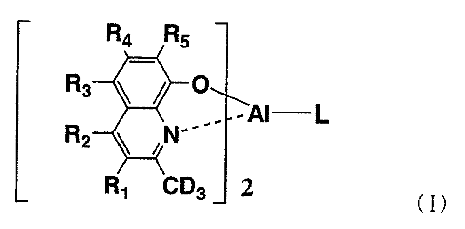
여기서, R1~R5는 각각 독립적으로, 수소원자, 중수소원자, 또는 알킬기, 아랄킬기, 알케닐기, 시아노기, 알콕시기, 치환기를 가지고 있어도 좋은 방향족 탄화수소기 또는 치환기를 가지고 있어도 좋은 방향족 복소환기에서 선택되는 1가의 치환기를 나타낸다. 여기서, 1가의 치환기가 수소원자를 가지는 경우는, 수소원자는 중수소원자여도 된다. D는 중수소원자를 나타낸다. L은 하기식 (1), (2), (3) 또는 (4)로 나타나는 1가의 기를 나타낸다; Herein, R 1 to R 5 each independently represent a hydrogen atom, a deuterium atom, or an alkyl group, an aralkyl group, an alkenyl group, a cyano group, an alkoxy group, or an aromatic heterocyclic group which may have a substituent. The monovalent substituent chosen from is shown. In the case where the monovalent substituent has a hydrogen atom, the hydrogen atom may be a deuterium atom. D represents a deuterium atom. L represents a monovalent group represented by the following formula (1), (2), (3) or (4);
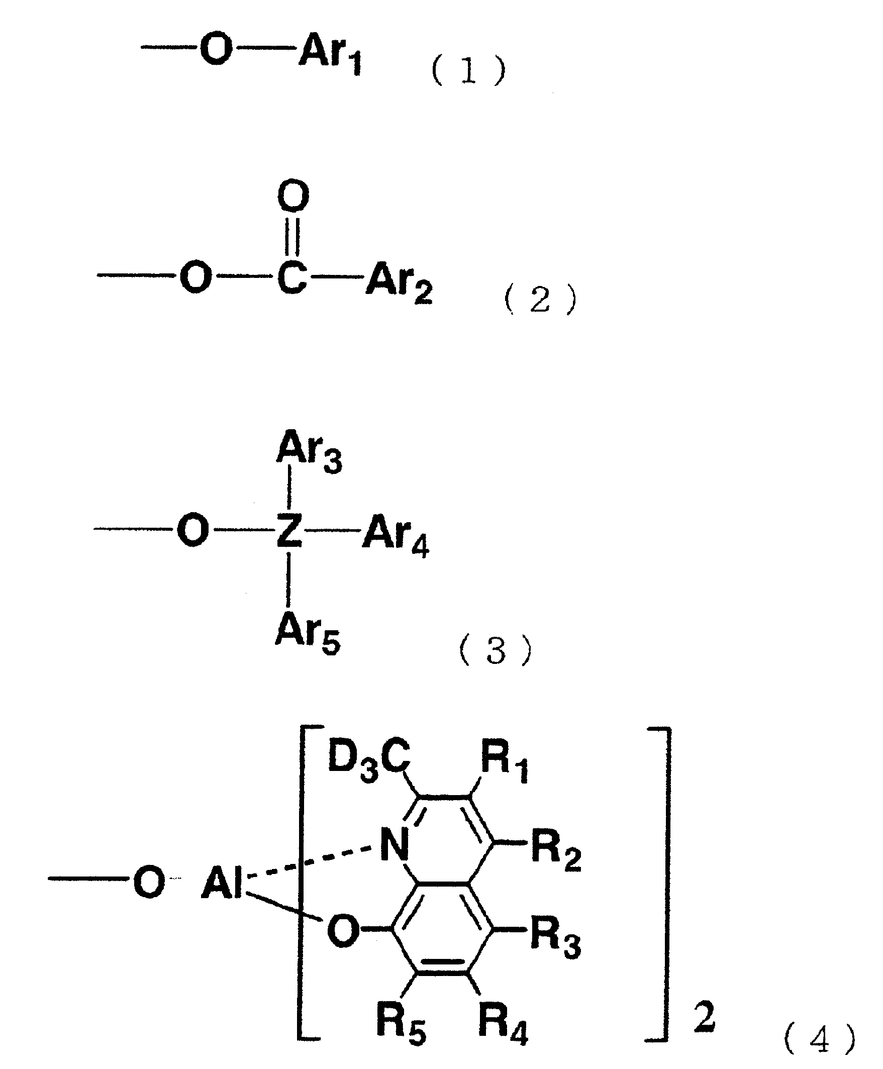
여기서, Ar1~Ar5는 각각 독립적으로, 치환기를 가지고 있어도 좋은 방향족 탄화수소기 또는 치환기를 가지고 있어도 좋은 방향족 복소환기를 나타내고, Z는 실리콘 또는 게르마늄을 나타낸다. R1~R5 및 D는 일반식 (I)과 같은 의미를 가진다. Here, Ar 1 to Ar 5 each independently represent an aromatic hydrocarbon group which may have a substituent or an aromatic heterocyclic group which may have a substituent, and Z represents silicon or germanium. R 1 to R 5 and D have the same meaning as in general formula (I).
바람직한 유기금속착물로서는, 하기 일반식 (II) 또는 (III)으로 표시되는 유기금속착물을 들 수 있다. As a preferable organometallic complex, the organometallic complex represented by the following general formula (II) or (III) is mentioned.

여기서, R1~R5 및 D는 일반식 (I)과 같은 의미를 가진다. 또, Ar1은 식 (1)과 같은 의미를 가지지만, 바람직하게는 1~3환의 방향족 탄화수소기이다. Here, R 1 to R 5 and D have the same meaning as in general formula (I). Ar 1 has the same meaning as in Formula (1), but is preferably a 1 to 3 ring aromatic hydrocarbon group.
본 발명의 유기 전계발광 소자는, 기판상에, 양극, 정공수송층, 발광층 및 전자수송층을 포함하는 유기층 그리고 음극이 적층되어 이루어지고, 적어도 1층의 유기층 중에 상기의 유기 전계발광 소자 재료를 포함한다. The organic electroluminescent device of the present invention is formed by stacking an organic layer including an anode, a hole transporting layer, a light emitting layer, and an electron transporting layer and a cathode on a substrate, and includes the organic electroluminescent device material in at least one organic layer. .
유리하게는, 유기 전계발광 소자는, 기판상에, 양극, 정공수송층, 발광층 및 전자수송층을 포함하는 유기층 그리고 음극이 적층되어 이루어지고, 발광층과 양극의 사이에 정공수송층을 가지고, 발광층과 음극의 사이에 전자수송층을 가지고, 발광층 중에 상기의 유기 전계발광 소자 재료를 포함한다. 더욱 유리하게는, 유기 전계발광 소자는, 발광층 중에, 상기의 유기 전계발광 소자 재료를 호스트 재료로서 함유하고, 주기율표 7~11족에서 선택되는 적어도 하나의 금속을 포함하는 유기금속착물을 게스트 재료로서 함유한다. Advantageously, the organic electroluminescent device comprises an organic layer comprising an anode, a hole transport layer, a light emitting layer and an electron transport layer and a cathode stacked on a substrate, and having a hole transport layer between the light emitting layer and the anode, It has an electron carrying layer in between, and includes said organic electroluminescent element material in a light emitting layer. More advantageously, the organic electroluminescent device comprises, as a guest material, an organic metal complex containing the above organic electroluminescent device material as a host material in the light emitting layer and containing at least one metal selected from
유기 전계발광 소자는, 양극 및 정공수송층간에 정공주입층이 배치되어 있는 것, 또는 음극 및 전자수송층간에 전자주입층이 배치되어 있는 것이 좋다. In the organic electroluminescent device, the hole injection layer is disposed between the anode and the hole transport layer, or the electron injection layer is disposed between the cathode and the electron transport layer.
본 발명의 유기 전계발광 소자 재료(유기 EL 재료)는, 상기 일반식 (I)로 표시되는 유기금속착물이다. 이러한 유기금속착물에 있어서, D가 H인 유기금속착물은, 상기 특허문헌 4, 8, 9 등에 있어서 알려져 있다. 따라서, 상기 일반식 (I)에 있어서의 R1, L 등의 기의 의미나, 바람직한 기는 이러한 문헌들로부터 이해된다. The organic electroluminescent element material (organic EL material) of the present invention is an organometallic complex represented by General Formula (I). In such an organometallic complex, an organometallic complex in which D is H is known in
일반식 (I)에 있어서, R1~R5는 각각 독립적으로, 수소원자, 중수소원자 또는 1가의 치환기를 나타낸다. 1가의 치환기는, 알킬기, 아랄킬기, 알케닐기, 시아노기, 알콕시기, 치환기를 가지고 있어도 좋은 방향족 탄화수소기 또는 치환기를 가지고 있어도 좋은 방향족 복소환기에서 선택된다. 여기서, 1가의 치환기가 수소원자를 가지는 경우, 그 수소원자는 D여도 된다. 바람직하게는, 1가의 치환기가 메틸기일 경우, CD3이다. In general formula (I), R <1> -R <5> represents a hydrogen atom, a deuterium atom, or a monovalent substituent each independently. The monovalent substituent is selected from an alkyl group, an aralkyl group, an alkenyl group, a cyano group, an alkoxy group, an aromatic hydrocarbon group which may have a substituent, or an aromatic heterocyclic group which may have a substituent. Here, when the monovalent substituent has a hydrogen atom, the hydrogen atom may be D. Preferably, when the monovalent substituent is a methyl group, it is CD 3 .
알킬기로서는, 탄소수 1~6의 알킬기(이하, 저급 알킬기라고 한다)가 바람직하게 예시되며, 아랄킬기로서는, 벤질기, 페네틸기가 바람직하게 예시되고, 알케닐기로서는, 탄소수 1~6의 저급 알케닐기가 바람직하게 예시되며, 알콕시기의 알킬부로서는, 저급 알킬이 바람직하게 예시된다. As an alkyl group, a C1-C6 alkyl group (henceforth a lower alkyl group) is illustrated preferably, As an aralkyl group, a benzyl group and a phenethyl group are illustrated preferably, As an alkenyl group, C1-C6 lower alkenyl A group is illustrated preferably, and lower alkyl is preferably illustrated as an alkyl part of an alkoxy group.
또, 방향족 탄화수소기로서는, 페닐기, 나프틸기, 아세나프틸기, 안트릴기 등의 방향족 탄화수소기가 바람직하게 예시되며, 방향족 복소환기로서는, 피리딜기, 퀴놀릴기, 티에닐기, 카르바졸기, 인돌릴기, 푸릴기 등의 방향족 복소환기가 바람직하게 예시된다. 이들이 치환기를 가지는 방향족 탄화수소기 또는 방향족 복소환기일 경우는, 치환기로서는, 저급 알킬기, 저급 알콕시기, 페녹시기, 벤질옥시기, 페닐기, 나프틸기 등을 들 수 있다. Moreover, as an aromatic hydrocarbon group, aromatic hydrocarbon groups, such as a phenyl group, a naphthyl group, an acenaphthyl group, an anthryl group, are illustrated preferably, As an aromatic heterocyclic group, a pyridyl group, a quinolyl group, thienyl group, a carbazole group, an indolyl group Aromatic heterocyclic groups, such as a furyl group, are illustrated preferably. When these are aromatic hydrocarbon groups or aromatic heterocyclic groups which have a substituent, a lower alkyl group, a lower alkoxy group, a phenoxy group, benzyloxy group, a phenyl group, a naphthyl group, etc. are mentioned.
L은 상기 식 (1), (2), (3) 또는 (4)로 표시되는 1가의 기를 나타내지만, Ar1~Ar5는 각각 독립적으로, 치환기를 가지고 있어도 좋은 방향족 탄화수소기 또는 치환기를 가지고 있어도 좋은 방향족 복소환기를 나타내고, Z는 실리콘 또는 게르마늄을 나타낸다. 여기서, 치환기를 가지고 있어도 좋은 방향족 탄화수소기 또는 치환기를 가지고 있어도 좋은 방향족 복소환기는, 상기와 같은 기가 예시된다. L represents a monovalent group represented by the formula (1), (2), (3) or (4), but Ar 1 to Ar 5 each independently have an aromatic hydrocarbon group or substituent which may have a substituent. An aromatic heterocyclic group which may be present is shown, and Z represents silicon or germanium. Here, the group similar to the above is illustrated in the aromatic hydrocarbon group which may have a substituent or the aromatic heterocyclic group which may have a substituent.
일반식 (I)로 표시되는 유기금속착물 중에서도, 바람직한 유기금속착물은 R1~R5가 수소원자, 저급 알킬기 또는 저급 알콕시기인 화합물에서 선택된다. 여기서, 저급 알킬기 또는 저급 알콕시기에 포함되는 수소원자는 D일 수 있다. 식 (1)~(3)에 있어서, 바람직한 Ar1, Ar2, Ar3으로서는, 1~3환의 방향족 탄화수소기를 들 수 있다. 또, L은 페녹시, 페닐페녹시, 나프톡시, 페닐나프톡시, 나프틸페녹시 등의 아릴옥시기 또는 식 (4)로 표시되는 1가의 기인 화합물에서 선택되는 것이 바람직하다. 식 (4)로 표시되는 1가의 기인 화합물일 경우는, 일반식 (II)로 표시되는 유기금속착물이 된다. Among the organometallic complexes represented by the general formula (I), preferred organometallic complexes are selected from compounds in which R 1 to R 5 are hydrogen atoms, lower alkyl groups or lower alkoxy groups. Here, the hydrogen atom included in the lower alkyl group or the lower alkoxy group may be D. In Formula (1)-(3), as preferable Ar <1> , Ar <2> , Ar <3> , a 1-3 ring aromatic hydrocarbon group is mentioned. In addition, L is preferably selected from an aryloxy group such as phenoxy, phenylphenoxy, naphthoxy, phenylnaphthoxy, naphthylphenoxy, or a monovalent group represented by formula (4). When it is a monovalent group compound represented by Formula (4), it becomes the organometallic complex represented by General formula (II).
이 일반식 (I)로 표시되는 유기금속착물은, 예를 들면, 대응하는 금속염과 식 (IV)로 표시되는 화합물과 식 (1a), (2a) 또는 (3a)로 표시되는 화합물을 2대1의 몰비로 착물 형성 반응함으로써 합성된다. 일반식 (II)로 표시되는 유기금속착물은, 대응하는 금속염과 식 (IV)로 표시되는 화합물과의 사이의 착물 형성 반응에 의해 합성된다. 또한, 식 (IV)에 있어서, R1~R5는 일반식 (I)의 R1~R5와 대응한다. 식 (1a), (2a) 및 (3a)로 표시되는 화합물은, 상기 식 (1), (2) 및 (3)으로 표시되는 1가의 기를 부여하고, Ar1~Ar5 및 Z는 식 (1), (2) 및 (3) 중의 Ar1~Ar5 및 Z에 대응한다. The organometallic complex represented by this general formula (I) is, for example, two metal compounds, a compound represented by formula (IV) and a compound represented by formula (1a), (2a) or (3a). It is synthesize | combined by making complex formation reaction in the molar ratio of 1. The organometallic complex represented by General Formula (II) is synthesized by a complex formation reaction between a corresponding metal salt and a compound represented by Formula (IV). In addition, in Formula (IV), R <1> -R <5> corresponds to R <1> -R <5> of general formula (I). The compounds represented by the formulas (1a), (2a) and (3a) give a monovalent group represented by the formulas (1), (2) and (3), and Ar 1 to Ar 5 and Z are represented by the formula (1). Corresponds to Ar 1 to Ar 5 and Z in 1), (2), and (3).
일반식 (II)로 표시되는 유기금속착물의 합성 반응은, 예를 들면, Y.Kushi 등이 제시하는 방법(J. Amer. Chem. Soc., vol.92, pp91,(1970))으로 행할 수 있다. 또한, 일반식 (II)에 있어서, R1~R5는 일반식 (I)의 R1~R5와 대응한다. 금속염으로서는, AlCl3, Al(Oi-Pr)3과 같은 화합물을 들 수 있다. The synthesis reaction of the organometallic complex represented by General Formula (II) can be carried out by, for example, the method proposed by Y. Kushi et al. (J. Amer. Chem. Soc., Vol. 92, pp91, (1970)). Can be. Further, in the general formula (II), and R 1 ~ R 5 are corresponding with the general formula (I) R 1 ~ R 5 . Examples of the metal salts include compounds such as AlCl 3 and Al (Oi-Pr) 3 .
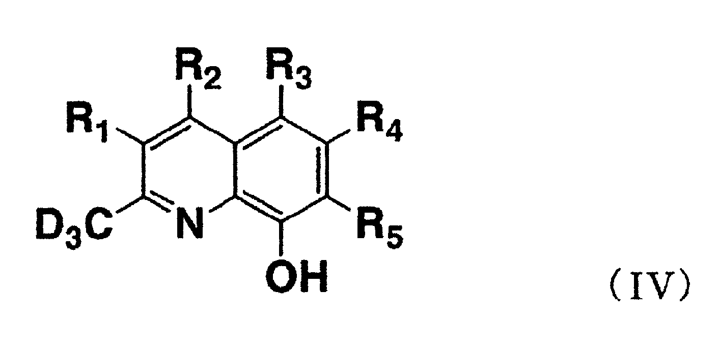

식 (IV)로 표시되는 화합물은, 예를 들면 메틸기의 수소가 H인 2-메틸-8-옥시퀴놀린(Me8HQ라고 한다)을 준비하고, 이 메틸기의 수소를 D로 함으로써 얻어진다. 이렇게 하여 얻어지는 Me8HQ의 메틸기의 수소가 D로 된 화합물을 Me8HQ-D라고 한다. 중수소화 반응 방법으로서는 공지의 조건을 채용할 수 있다. 예를 들면, Me8HQ와 중수를 Pd/C 촉매의 존재하에서, 150~200℃에서 반응시킴으로써 메틸기의 수소를 선택적으로 중수소화할 수 있다. 또한, 일반식 (I)에 있어서, R1~R5가 H일 경우나, H를 가지는 알킬기 등일 경우는, 반응 조건에 따라서는 이들의 H의 일부도 중수소화되지만, 지장은 없다. 그러나, 2위의 메틸기의 수소의 중수소화율은 40% 이상, 바람직하게는 90% 이상, 보다 바람직하게는 95% 이상으로 하는 것이 좋다. 따라서, 본 발명의 일반식 (I)로 표시되는 유기금속착물은 2위의 메틸기가 CD3인 것을 주로 하는 것이면 되며, 소량의 CD2H, CDH2 또는 CH3을 포함할 수 있다. The compound represented by Formula (IV) is obtained by preparing 2-methyl-8-oxyquinoline (called Me8HQ) whose hydrogen of a methyl group is H, for example, and making hydrogen of this methyl group into D. The compound whose hydrogen of the methyl group of Me8HQ obtained in this way becomes D is called Me8HQ-D. As a deuteration reaction method, well-known conditions can be employ | adopted. For example, hydrogen of the methyl group can be selectively deuterated by reacting Me8HQ and heavy water at 150 to 200 ° C in the presence of a Pd / C catalyst. In general formula (I), when R <1> -R <5> is H, and when it is an alkyl group etc. which have H, some of these H also deuterated depending on reaction conditions, but it does not interfere. However, the deuteration rate of hydrogen of the second methyl group is preferably at least 40%, preferably at least 90%, more preferably at least 95%. Therefore, the organometallic complex represented by the general formula (I) of the present invention only needs to have the second methyl group of CD 3 and may include a small amount of CD 2 H, CDH 2 or CH 3 .
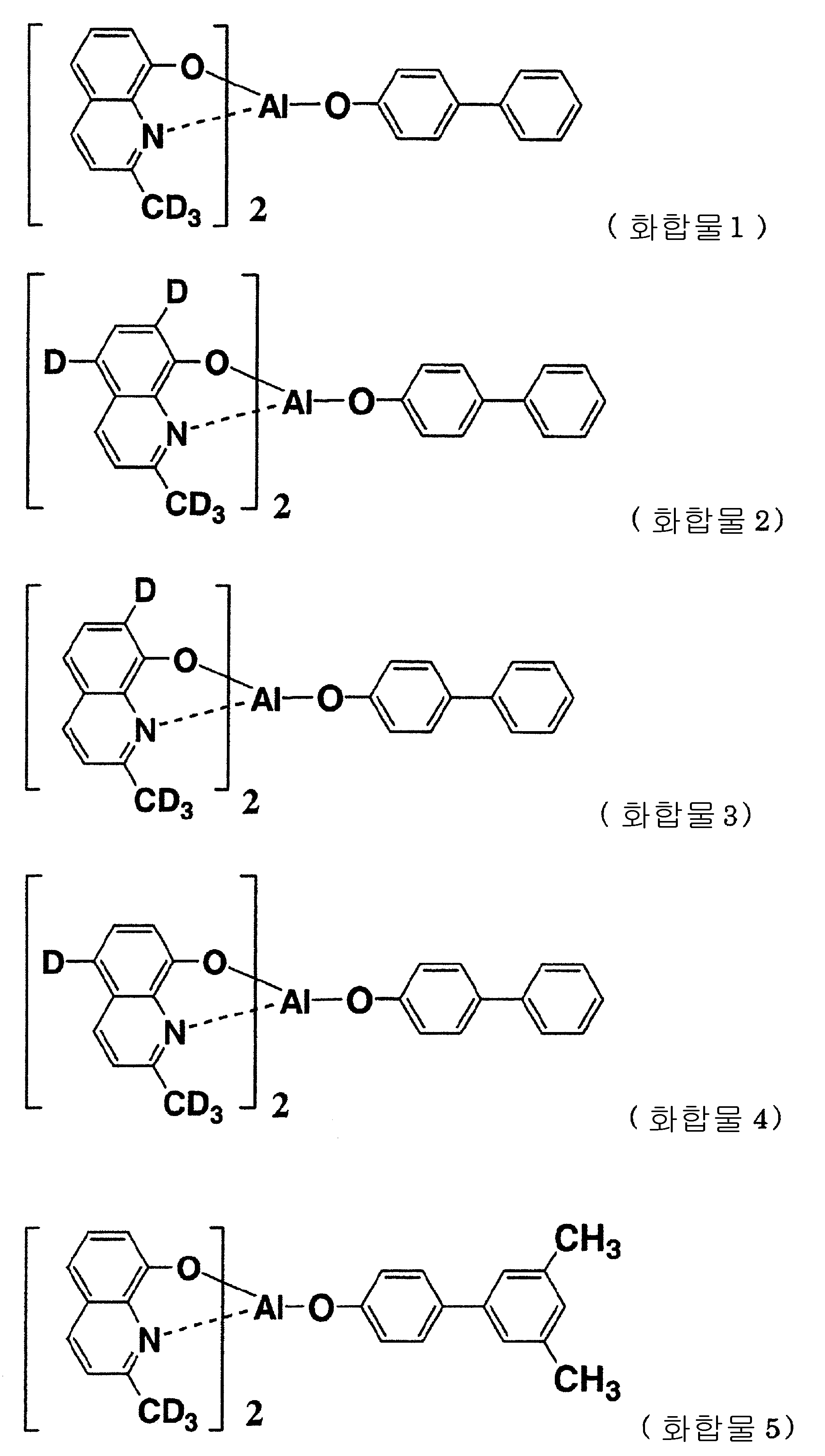
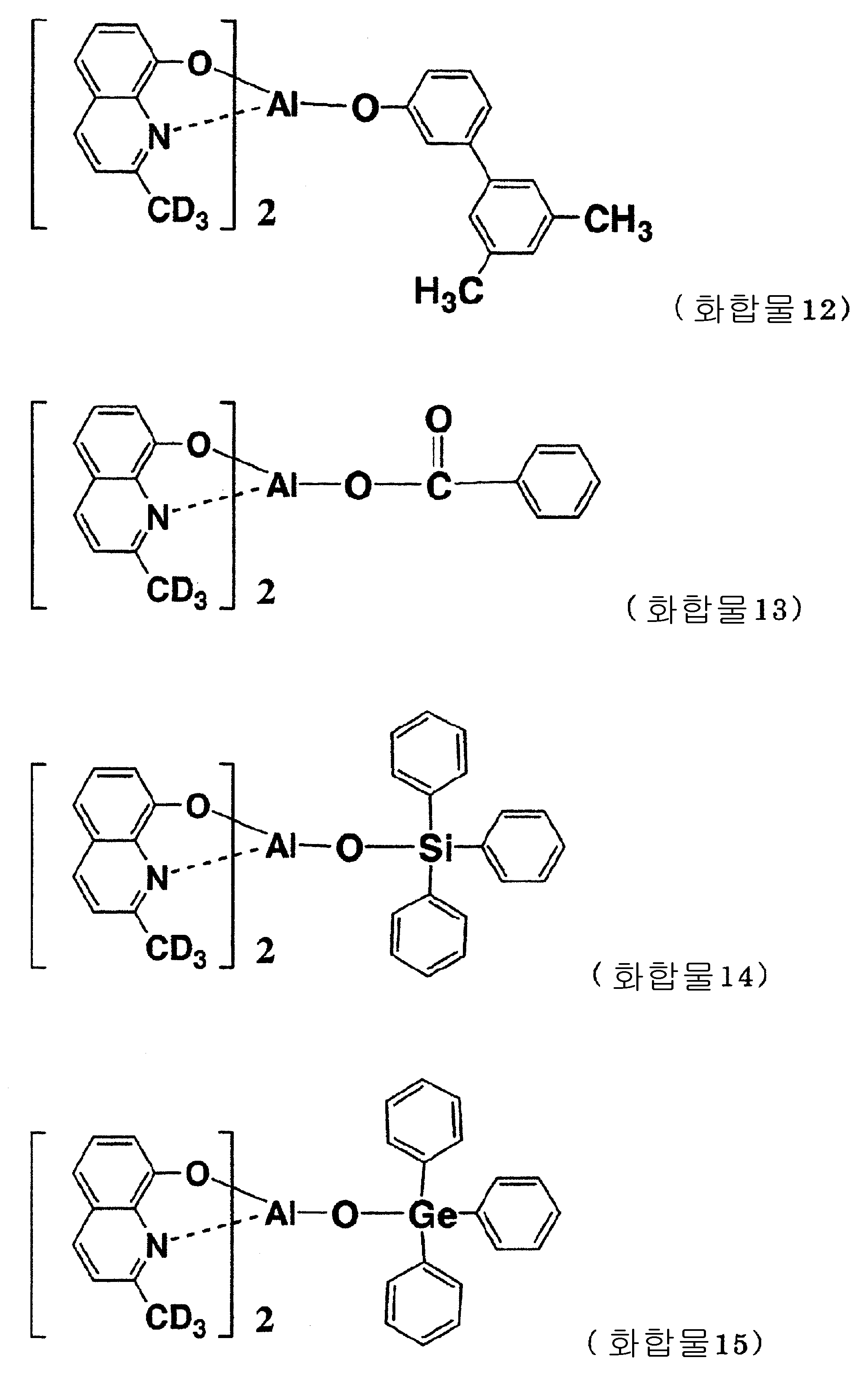
이하에 일반식 (I)로 표시되는 유기금속착물로 이루어지는 본 발명의 유기 EL 재료를 예시하지만, 하기의 화합물에 한정되는 것이 아니다. Although the organic EL material of this invention which consists of the organometallic complex represented by General formula (I) below is illustrated, it is not limited to the following compound.


본 발명의 유기 EL 소자는, 일반식 (I)로 표시되는 유기금속착물로 이루어지는 본 발명의 유기 EL 재료를 적어도 1층의 유기층 중에 포함한다. 유기 EL 소자는, 양극, 정공수송층, 발광층 및 전자수송층을 포함하는 유기층 그리고 음극이 적층되어 있는 구조를 가진다. 바람직하게는, 기판상에, 양극, 정공수송층, 발광층 및 전자수송층을 포함하는 유기층 그리고 음극이 적층되어 이루어지고, 발광층과 양극의 사이에 정공수송층을 가지고, 발광층과 음극의 사이에 전자수송층을 가지는 구조이다. 더 유리하게는, 양극 및 정공수송층간에 정공주입층이 배치되어 있는 구조 또는 음극 및 전자수송층간에 전자주입층이 배치되어 있는 구조이다. The organic electroluminescent element of this invention contains the organic electroluminescent material of this invention which consists of an organometallic complex represented by General formula (I) in at least one organic layer. The organic EL device has a structure in which an organic layer including an anode, a hole transport layer, a light emitting layer, and an electron transport layer and a cathode are stacked. Preferably, an organic layer including an anode, a hole transport layer, a light emitting layer and an electron transport layer and a cathode are laminated on the substrate, and have a hole transport layer between the light emitting layer and the anode, and an electron transport layer between the light emitting layer and the cathode. Structure. More advantageously, the hole injection layer is arranged between the anode and the hole transport layer or the electron injection layer is arranged between the cathode and the electron transport layer.
본 발명의 유기 EL 재료는 발광 재료로서 발광층에 포함되는 것이 바람직하다. 유리하게는, 본 발명의 유기 EL 재료를 발광층 중에 호스트 재료로서 함유하고, 또한 주기율표 7 내지 11족에서 선택되는 적어도 하나의 금속을 포함하는 유기금속착물을 게스트 재료로서 발광층에 함유하는 것이다. 그러나, 다른 층의 재료로서 사용하는 것도 가능해서, 예를 들면 정공저지재료로서 사용하는 것도 가능하다. It is preferable that the organic EL material of this invention is contained in a light emitting layer as a light emitting material. Advantageously, the organic EL material of the present invention is contained in the light emitting layer as a host material, and an organic metal complex containing at least one metal selected from
발광층 중에, 본 발명의 유기 EL 재료를 호스트 재료로서 함유하고, 게스트 재료를 함유하는 경우는, 소위 인광을 이용한 유기 EL 소자가 된다. 여기서, 호스트 재료란, 상기 층을 형성하는 재료 중 50중량% 이상을 차지하는 것을 의미하고, 게스트 재료란, 상기 층을 형성하는 재료 중 50중량% 미만을 차지하는 것을 의미한다. 본 발명의 유기 EL 소자에 있어서, 발광층에 포함되는 본 발명의 유기 EL 재료는, 상기 층에 포함되는 인광성 유기금속착물의 여기 삼중항 준위보다 높은 에너지 상태의 여기 삼중항 준위를 가지는 것이 기본적으로 필요하다. In the light emitting layer, when the organic EL material of the present invention is contained as a host material and a guest material is contained, it becomes an organic EL device using so-called phosphorescence. Here, the host material means that it occupies 50% by weight or more of the material forming the layer, and the guest material means less than 50% by weight of the material forming the layer. In the organic EL device of the present invention, the organic EL material of the present invention included in the light emitting layer basically has an excitation triplet level of an energy state higher than the excitation triplet level of the phosphorescent organometallic complex contained in the layer. need.
호스트 재료로서는, 안정된 박막형상을 부여하고 또는 높은 Tg를 가지고, 정공 또는 전자를 효율적으로 수송할 수 있는 화합물인 것이 필요하다. 나아가, 전기화학적으로 또한 화학적으로 안정되며, 트랩이 되거나 발광을 소광하거나 하는 불순물이 제조시나 사용시에 발생하기 어려운 화합물인 것이 요구되는 동시에, 인광성 유기착물의 발광이 정공수송층의 여기 삼중항 준위에 영향받기 어렵게 하기 위해서, 발광 영역이 정공수송층 계면으로부터도 적당히 거리를 유지할 수 있는 정공주입 능력을 가지는 것도 중요하다. 본 발명의 유기 EL 재료는 이러한 조건들을 만족하는 점에서 우수하다. As the host material, it is necessary to be a compound which gives a stable thin film shape or has a high Tg and can efficiently transport holes or electrons. Furthermore, it is required to be an electrochemically and chemically stable compound that is difficult to occur during manufacture or use as an impurity that traps or quenchs light emission, and the emission of the phosphorescent organic complex is brought to the excitation triplet level of the hole transport layer. In order to be less likely to be affected, it is also important that the light emitting region has a hole injection ability capable of keeping a proper distance from the hole transport layer interface. The organic EL material of the present invention is excellent in satisfying these conditions.
게스트 재료로서는, 바람직하게는 주기율표에서 7~11족의 금속을 함유하는 유기금속착물이다. 보다 바람직하게는 8족의 금속을 함유하는 유기금속착물이다. 더욱 바람직하게는, 이리듐, 오스뮴, 로듐, 팔라듐 또는 백금에서 선택되는 금속을 함유하는 유기금속착물이다. 그 중에서도 바람직하게는 이리듐, 로듐, 백금에서 선택되는 금속을 함유하는 유기금속착물이며, 가장 바람직하게는 이리듐을 함유하는 유기금속착물이다. As a guest material, Preferably it is the organometallic complex containing a metal of group 7-11 in a periodic table. More preferably, it is an organometallic complex containing a metal of
게스트 재료로서는, 일반적으로는 상기 특허문헌에 기재되어 있는 화합물 등을 들 수 있지만, 이들에 한정되는 것이 아니다. Generally as a guest material, although the compound etc. which are described in the said patent document are mentioned, it is not limited to these.
이하에, 게스트 재료의 구체예를 나타내지만, 이들에 한정되는 것은 아니다. 이러한 화합물들은, 예를 들면 Inorg. Chem., vol.40, pp1704~1711에 기재된 방법 등에 의해 합성할 수 있다. Although the specific example of a guest material is shown below, it is not limited to these. Such compounds are described, for example, in Inorg. It can synthesize | combine by the method etc. of Chem., Vol.40, pp1704-1711.


도 1은 유기 전계발광 소자의 일례를 나타낸 모식 단면도이다. 1: is a schematic cross section which shows an example of an organic electroluminescent element.
도 2는 Me8HQ-D1의 IR 스펙트럼이다. 2 is an IR spectrum of Me8HQ-D1.
도 3은 Me8HQ와 Me8HQ-D1의 NMR 스펙트럼(δ7.0~9.0)이다. 3 is an NMR spectrum (δ7.0 to 9.0) of Me8HQ and Me8HQ-D1.
도 4는 Me8HQ와 Me8HQ-D1의 NMR 스펙트럼(δ2.0~3.0)이다.4 is an NMR spectrum (δ2.0 to 3.0) of Me8HQ and Me8HQ-D1.
도 5는 BAlq-D4의 FD-MS 스펙트럼이다.5 is an FD-MS spectrum of BAlq-D4.
도 6은 BAlq-D4의 IR 스펙트럼이다.6 is an IR spectrum of BAlq-D4.
도 7은 AQD-D7의 FD-MS 스펙트럼이다.7 is an FD-MS spectrum of AQD-D7.
도 8은 AQD-D7의 IR 스펙트럼이다.8 is an IR spectrum of AQD-D7.
<부호의 설명><Description of Symbols>
1 기판1 board
2 양극2 anode
3 정공주입층3 hole injection layer
4 정공수송층4 hole transport layer
5 발광층5 emitting layer
6 전자수송층6 electron transport layer
7 음극 7 cathode
이하, 본 발명의 유기 EL 소자에 대해서, 도면을 참조하면서 설명한다. 도 1은 본 발명에서 사용되는 일반적인 유기 EL 소자의 구조예를 모식적으로 나타내는 단면도이다. 본 발명의 유기 EL 소자에서는, 기판, 양극, 정공수송층, 발광층, 전자수송층 및 음극을 필수 층으로서 가지지만, 필수 층 이외의 층, 예를 들면, 정공주입층은 생략 가능하며, 또 필요에 따라 다른 층을 형성해도 된다. 또한, 정공저지층을 형성하지 않음으로 인해 층 구조가 간소화되는 등의 이점을 초래하는 일이 있다. EMBODIMENT OF THE INVENTION Hereinafter, the organic electroluminescent element of this invention is demonstrated, referring drawings. 1 is a cross-sectional view schematically showing a structural example of a general organic EL device used in the present invention. In the organic EL device of the present invention, the substrate, the anode, the hole transport layer, the light emitting layer, the electron transport layer and the cathode are essential layers, but layers other than the essential layer, for example, the hole injection layer, can be omitted. You may form another layer. In addition, since the hole blocking layer is not formed, the layer structure may be simplified.
기판(1)은 유기 전계발광 소자의 지지체가 되는 것으로서, 석영이나 유리 판, 금속판이나 금속박, 플라스틱 필름이나 시트 등이 사용된다. 특히 유리판이나, 폴리에스테르, 폴리메타크릴레이트, 폴리카보네이트, 폴리설폰 등의 투명한 합성수지의 판이 바람직하다. 합성수지기판을 사용하는 경우에는 가스 배리어성에 유의할 필요가 있다. 기판의 가스 배리어성이 지나치게 작으면, 기판을 통과한 외기에 의 해 유기 전계발광 소자가 열화하는 일이 있으므로 바람직하지 않다. 이 때문에, 합성수지기판의 적어도 한쪽면에 치밀한 실리콘 산화막 등을 형성해서 가스 배리어성을 확보하는 방법도 바람직한 방법 중 하나이다. The board |
기판(1) 상에는 양극(2)이 형성되는데, 양극은 정공수송층으로의 정공주입의 역할을 하는 것이다. 이 양극은, 통상, 알루미늄, 금, 은, 니켈, 팔라듐, 백금 등의 금속, 인듐 및/또는 주석의 산화물 등의 금속산화물, 요오드화구리 등의 할로겐화 금속, 카본블랙, 혹은, 폴리(3-메틸티오펜), 폴리피롤, 폴리아닐린 등의 도전성 고분자 등에 의해 구성된다. 양극의 형성은 통상 스퍼터링법, 진공증착법 등에 의해 행해지는 일이 많다. 또, 은 등의 금속미립자, 요오드화구리 등의 미립자, 카본블랙, 도전성의 금속산화물 미립자, 도전성 고분자 미분말 등의 경우에는, 적당한 바인더 수지용액에 분산시켜, 기판(1) 상에 도포함으로써 양극(2)을 형성할 수도 있다. 또한, 도전성 고분자의 경우는 전해 중합에 의해 직접 기판(1) 상에 박막을 형성하거나, 기판(1) 상에 도전성 고분자를 도포해서 양극(2)을 형성할 수도 있다. 양극은 다른 물질로 적층해서 형성하는 것도 가능하다. 양극의 두께는 필요로 하는 투명성에 따라 다르다. 투명성이 필요해지는 경우는, 가시광의 투과율을 통상 60% 이상, 바람직하게는 80% 이상으로 하는 것이 바람직하고, 이 경우, 두께는 통상 5~1000nm, 바람직하게는 10~500nm 정도이다. 불투명으로 좋은 경우, 양극(2)은 기판(1)과 동일해도 된다. 또, 나아가서는 상기의 양극(2)의 위에 다른 도전재료를 적층하는 것도 가능하다. The
양극(2)의 위에는 정공수송층(4)이 형성된다. 양자 사이에는 정공주입층(3) 을 형성할 수도 있다. 정공수송층의 재료에 요구되는 조건으로서는, 양극으로부터의 정공주입 효율이 높고, 또한, 주입된 정공을 효율적으로 수송할 수 있는 재료인 것이 필요하다. 그를 위해서는, 이온화 포텐셜이 작고, 가시광의 광에 대하여 투명성이 높고, 게다가 정공이동도가 크고, 또한 안정성이 뛰어나며, 트랩이 되는 불순물이 제조시나 사용시에 발생하기 어려운 것이 요구된다. 또, 발광층(5)에 접하기 때문에 발광층으로부터의 발광을 소광하거나, 발광층과의 사이에서 엑시플렉스(exciplex)를 형성해서 효율을 저하시키지 않는 것이 요구된다. 상기의 일반적 요구 외에, 차재(車載) 표시용의 응용을 고려한 경우, 소자에는 내열성이 더욱 요구된다. 따라서, Tg로서 85℃ 이상의 값을 가지는 재료가 바람직하다. 바람직한 정공수송재료로서 α-NPD와 같은 공지의 트리아릴아민다이머를 사용할 수 있다. The hole transport layer 4 is formed on the
또한, 필요에 따라 기타 정공수송재료로서 공지의 화합물을 트리아릴아민다이머와 병용할 수도 있다. 예를 들면, 2개 이상의 3급 아민을 포함하여 2개 이상의 축합방향족환이 질소원자로 치환한 방향족 디아민, 4,4',4''-트리스(1-나프틸페닐아미노)트리페닐아민 등의 스타버스트(starburst) 구조를 가지는 방향족 아민 화합물, 트리페닐아민의 4량체로 이루어지는 방향족 아민 화합물, 2,2',7,7'-테트라키스-(디페닐아미노)-9,9'-스피로비플루오렌 등의 스피로 화합물 등을 들 수 있다. 이러한 화합물들은 단독으로 사용해도 되고, 필요에 따라서 각각 혼합해서 사용해도 된다. 또, 상기의 화합물 이외에, 정공수송층의 재료로서, 폴리비닐카르바졸, 폴리비닐트리페닐아민, 테트라페닐벤지딘을 함유하는 폴리아릴렌에테르설폰 등의 고분자 재료를 들 수 있다. If necessary, a known compound may be used in combination with a triarylamine dimer as other hole transport materials. For example, an aromatic diamine in which two or more condensed aromatic rings including two or more tertiary amines are substituted with nitrogen atoms, and a star such as 4,4 ', 4' '-tris (1-naphthylphenylamino) triphenylamine. Aromatic amine compound having a starburst structure, aromatic amine compound consisting of a tetramer of triphenylamine, 2,2 ', 7,7'-tetrakis- (diphenylamino) -9,9'-spirobiflu Spiro compounds, such as orene, etc. are mentioned. These compounds may be used alone, or may be mixed and used as necessary. In addition to the above compounds, polymer materials such as polyarylene ether sulfone containing polyvinylcarbazole, polyvinyltriphenylamine and tetraphenylbenzidine can be mentioned as the material of the hole transport layer.
정공수송층을 도포법으로 형성하는 경우는, 정공수송재료를 1종 이상과, 필요에 따라 정공의 트랩이 되지 않는 바인더 수지나 도포성 개량제 등의 첨가제를 첨가하고, 용해해서 도포 용액을 조제하고, 스핀코트법 등의 방법에 의해 양극(2) 상에 도포하고, 건조해서 정공수송층(4)을 형성한다. 바인더 수지로서는, 폴리카보네이트, 폴리아릴레이트, 폴리에스테르 등을 들 수 있다. 바인더 수지는 첨가량이 많으면 정공이동도를 저하시키므로 적은 쪽이 바람직하고, 통상 50중량% 이하가 바람직하다. In the case of forming the hole transport layer by the coating method, at least one hole transport material is added, and additives such as binder resins or coatability improving agents which do not trap holes as necessary, are dissolved, and a coating solution is prepared. It is apply | coated on the
진공증착법으로 형성하는 경우는, 정공수송재료를 진공용기 내에 설치된 도가니(crucible)에 넣고, 진공용기 내를 적당한 진공 펌프로 10-4Pa 정도로까지 배기한 후, 도가니를 가열하여 정공수송재료를 증발시켜, 도가니와 서로 마주보고 놓여진, 양극이 형성된 기판상에 정공수송층(4)을 형성시킨다. 정공수송층(4)의 막두께는 통상 5~300nm, 바람직하게는 10~100nm이다. 이와 같이 얇은 막을 일률적으로 형성하기 위해서는, 일반적으로 진공증착법이 잘 이용된다. In the case of forming by vacuum evaporation, the hole transport material is placed in a crucible installed in a vacuum container, the inside of the vacuum container is evacuated to about 10 -4 Pa with a suitable vacuum pump, and the crucible is heated to evaporate the hole transport material. In this way, the hole transport layer 4 is formed on the anode-formed substrate placed facing the crucible. The film thickness of the hole transport layer 4 is usually 5 to 300 nm, preferably 10 to 100 nm. In order to form such a thin film uniformly, vacuum deposition is generally used well.
정공수송층(4)의 위에는 발광층(5)이 형성된다. 발광층(5)은, 상기 일반식 (I)로 표시되는 유기금속착물 또는 그 혼합물과, 상기와 같은 게스트 재료(예를 들면, Ir 착물)를 함유하고, 전계를 부여받은 전극간에 있어서, 양극으로부터 주입되어 정공수송층을 이동하는 정공과, 음극으로부터 주입되어 전자수송층(6)을 이동하는 전자와의 재결합에 의해 여기되어서, 강한 발광을 나타낸다. 또한 발광층(5)은, 본 발명의 성능을 손상하지 않는 범위에서, 다른 호스트 재료(일반식 (I)과 같은 작용을 행한다)나 형광 색소 등, 타 성분을 포함하고 있어도 된다. The light emitting layer 5 is formed on the hole transport layer 4. The light emitting layer 5 contains an organometallic complex represented by the general formula (I) or a mixture thereof and the above guest material (for example, Ir complex), and is formed from an anode between the electrodes provided with an electric field. It is excited by recombination of holes injected and moving the hole transport layer and electrons injected from the cathode and moving the
게스트 재료가 발광층 중에 함유되는 양은 0.1~30중량%의 범위에 있는 것이 바람직하다. 0.1중량% 이하에서는 소자의 발광 효율 향상에 기여할 수 없고, 30중량%를 넘으면 유기금속착물끼리가 이량체를 형성하는 등의 농도 소광이 일어나, 발광 효율의 저하에 이른다. 종래의 형광(일중항)을 사용한 소자에 있어서, 발광층에 함유되는 형광성 색소(도펀트)의 양보다 약간 많은 쪽이 바람직한 경향이 있다. 게스트 재료가 발광층 중에 막두께 방향에 대해서 부분적으로 포함되거나, 불균일하게 분포되어도 된다. It is preferable that the quantity which a guest material contains in a light emitting layer exists in the range of 0.1-30 weight%. If it is 0.1 weight% or less, it cannot contribute to the improvement of the luminous efficiency of an element, and when it exceeds 30 weight%, concentration quenching, such as an organic metal complex forming a dimer, will arise, and it will fall in luminous efficiency. In a device using a conventional fluorescence (single term), a slightly larger amount than the amount of the fluorescent dye (dopant) contained in the light emitting layer tends to be preferable. The guest material may be partially contained in the light emitting layer with respect to the film thickness direction or may be unevenly distributed.
발광층(5)의 막두께는 통상 10~200nm, 바람직하게는 20~100nm이다. 정공수송층(4)과 같은 방법으로 박막형성된다. The film thickness of the light emitting layer 5 is 10-200 nm normally, Preferably it is 20-100 nm. The thin film is formed in the same manner as the hole transport layer 4.
소자의 발광 효율을 더욱 향상시키는 것을 목적으로 해서, 발광층(5)과 음극(7)의 사이에 전자수송층(6)이 형성된다. 전자수송층(6)은, 전계를 부여받은 전극간에 있어서 음극으로부터 주입된 전자를 효율적으로 발광층(5)의 방향으로 수송할 수 있는 화합물로 형성된다. 전자수송층(6)에 사용되는 전자수송성 화합물로서는, 음극(7)으로부터의 전자주입효율이 높고, 또한, 높은 전자이동도를 가지고 주입된 전자를 효율적으로 수송할 수 있는 화합물인 것이 필요하다. For the purpose of further improving the luminous efficiency of the device, the
이러한 조건을 만족하는 전자수송재료로서는, Alq3 등의 금속착물, 10-하이드록시벤조[h]퀴놀린의 금속착물, 옥사디아졸 유도체, 디스티릴비페닐 유도체, 실롤 유도체, 3- 또는 5-하이드록시플라본 금속착물, 벤즈옥사졸 금속착물, 벤조티아졸 금속착물, 트리스벤즈이미다졸릴벤젠, 퀴녹살린 화합물, 페난트롤린 유도체, 2- t-부틸-9,10-N,N'-디시아노안트라퀴논디이민, n형 수소화 비정질 탄화 실리콘, n형 황화 아연, n형 셀렌화 아연 등을 들 수 있다. 전자수송층(6)의 막두께는 통상 5~200nm, 바람직하게는 10~100nm이다. 전자수송층(6)은, 정공수송층(4)과 마찬가지로 해서 도포법 혹은 진공증착법에 의해 발광층(5) 상에 적층함으로써 형성된다. 통상은 진공증착법이 이용된다. Examples of the electron transporting material that satisfies these conditions include metal complexes such as Alq3, metal complexes of 10-hydroxybenzo [h] quinoline, oxadiazole derivatives, distyryl biphenyl derivatives, silol derivatives, and 3- or 5-hydroxyflavones. Metal complexes, benzoxazole metal complexes, benzothiazole metal complexes, trisbenzimidazolylbenzenes, quinoxaline compounds, phenanthroline derivatives, 2-t-butyl-9,10-N, N'-dicyanoanthraqui Non-diimine, n-type hydrogenated amorphous silicon carbide, n-type zinc sulfide, n-type zinc selenide, etc. are mentioned. The film thickness of the
정공주입의 효율을 더욱 향상시키고, 또한, 유기층 전체의 양극에의 부착력을 개선시킬 목적으로, 정공수송층(4)과 양극(2) 사이에 정공주입층(3)을 형성하는 것도 행해지고 있다. 정공주입층(3)을 형성함으로써, 초기 소자의 구동 전압이 내려감과 동시에, 소자를 정전류로 연속 구동했을 때의 전압 상승도 억제되는 효과가 있다. 정공주입층에 사용되는 재료에 요구되는 조건으로서는, 양극과의 밀착성이 좋고 균일한 박막을 형성할 수 있으며, 열적으로 안정된 것이 요망된다. 즉, 융점 및 유리전이온도가 높고, 융점으로서는 300℃ 이상, 유리전이온도로서는 100℃ 이상이 요구된다. 또한, 이온화 포텐셜이 낮고 양극으로부터의 정공주입이 용이한 것, 정공이동도가 큰 것이 요망된다. Forming the hole injection layer 3 between the hole transport layer 4 and the
이 목적을 위해서, 지금까지 구리 프탈로시아닌 등의 프탈로시아닌 화합물, 폴리아닐린, 폴리티오펜 등의 유기 화합물이나, 스퍼터 카본막이나, 바나듐 산화물, 루테늄 산화물, 몰리브덴 산화물 등의 금속산화물이 보고되어 있다. 정공주입층의 경우도, 정공수송층과 마찬가지로 해서 박막이 형성 가능하지만, 무기물의 경우에는, 스퍼터법이나 전자 빔 증착법, 플라즈마 CVD법이 또한 이용된다. 이상과 같이 해서 형성되는 양극 버퍼층(3)의 막두께는 통상 3~100nm, 바람직하게는 5~50nm이다. For this purpose, organic compounds such as phthalocyanine compounds such as copper phthalocyanine, polyaniline and polythiophene, metal oxides such as sputtered carbon film, vanadium oxide, ruthenium oxide and molybdenum oxide have been reported. In the case of the hole injection layer, a thin film can be formed in the same manner as the hole transport layer. However, in the case of the inorganic material, a sputtering method, an electron beam vapor deposition method, and a plasma CVD method are also used. The film thickness of the anode buffer layer 3 formed as mentioned above is 3-100 nm normally, Preferably it is 5-50 nm.
음극(7)은 발광층(5)에 전자를 주입하는 역할을 한다. 음극으로서 사용되는 재료는, 상기 양극(2)에 사용되는 재료를 사용하는 것이 가능하지만, 효율적으로 전자주입을 행하기 위해서는 일함수가 낮은 금속이 바람직하며, 주석, 마그네슘, 인듐, 칼슘, 알루미늄, 은 등의 적당한 금속 또는 그들의 합금이 사용된다. 구체예로서는, 마그네슘-은 합금, 마그네슘-인듐 합금, 알루미늄-리튬 합금 등의 저일함수(low-work-function) 합금 전극을 들 수 있다. The
음극(7)의 막두께는 통상 양극(2)과 같다. 저일함수 금속으로 이루어지는 음극을 보호하는 목적으로, 이 위에 일함수가 높고 대기에 대해 안정된 금속층을 또한 적층하는 것은 소자의 안정성을 늘린다. 이 목적을 위해, 알루미늄, 은, 구리, 니켈, 크롬, 금, 백금 등의 금속이 사용된다. The film thickness of the
또한, 음극과 전자수송층의 사이에 LiF, MgF2, Li2O 등의 극박 절연막(0.1~5nm)을 전자주입층으로서 삽입하는 것도 소자의 효율을 향상시키는 유효한 방법이다. In addition, inserting an ultrathin insulating film (0.1-5 nm) such as LiF, MgF 2 , Li 2 O, or the like as an electron injection layer between the cathode and the electron transport layer is an effective method for improving the efficiency of the device.
또한, 도 1과는 반대의 구조, 즉, 기판(1) 상에 음극(7), 전자수송층(6), 발광층(5), 정공수송층(4), 양극(2)의 순으로 적층하는 것도 가능하며, 이미 서술한 바와 같이 적어도 한쪽이 투명성이 높은 2매의 기판 사이에 본 발명의 유기 EL 소자를 형성하는 것도 가능하다. 이 경우도, 필요에 따라 층을 추가하거나, 생략하거나 하는 것이 가능하다. In addition, the structure opposite to that of FIG. 1, that is, the
본 발명은, 유기 EL 소자가, 단일 소자, 어레이 형상으로 배치된 구조로 이루어지는 소자, 양극과 음극이 X-Y 매트릭스 형상으로 배치된 구조 중 어느 쪽에 있어서도 적용할 수 있다. 본 발명의 유기 EL 소자에 의하면, 발광층에 특정한 골격을 가지는 화합물과, 인광성의 금속착물을 함유시킴으로써, 종래의 일중항 상태로부터의 발광을 이용한 소자보다도 발광 효율이 높으면서 또한 구동 안정성에 있어서도 크게 개선된 소자가 얻어져, 풀 컬러 혹은 멀티 컬러 패널로의 응용에 있어서 뛰어난 성능을 발휘할 수 있다. The present invention can be applied to either of a single device, a device having a structure in which the array is arranged in an array, and a structure in which the anode and the cathode are arranged in an X-Y matrix. According to the organic EL device of the present invention, by containing a compound having a specific skeleton in the light emitting layer and a phosphorescent metal complex, the luminous efficiency is higher than that of the device using light emission from the conventional singlet state, and the driving stability is greatly improved. An element is obtained and can exhibit the outstanding performance in the application to a full color or a multi color panel.
<실시예><Examples>
다음으로, 본 발명을 합성예 및 실시예에 의해 더욱 자세하게 설명하지만, 본 발명은 그 요지를 넘지 않는 한, 이하의 실시예의 기재에 한정되는 것은 아니다. Next, although this invention is demonstrated further in detail by the synthesis example and the Example, this invention is not limited to description of the following Example unless the summary is exceeded.
약호를 다음에 나타낸다. The abbreviation is shown below.
Me8HQ: 2-메틸-8-하이드록시퀴놀린 Me8HQ: 2-methyl-8-hydroxyquinoline
Me8HQ-D: 중수소화 Me8HQ Me8HQ-D: Deuterated Me8HQ
BAlq: p-페닐페놀라토-비스(2-메틸-8-퀴놀리노라토-N1,O8)알루미늄BAlq: p-phenylphenolato-bis (2-methyl-8-quinolinolato-N1, O8) aluminum
BAlq-D: 중수소화 BAlq(화합물 1)BAlq-D: Deuterated BAlq (Compound 1)
AQD: 알루미늄퀴놀리놀다이머(화합물 20) AQD: Aluminum Quinolinol Dimer (Compound 20)
AQD-D: 중수소화 AQD(화합물 21) AQD-D: Deuterated AQD (Compound 21)

합성예 1 Synthesis Example 1
Me8HQ 8.0g과 중수(重水) 77g을 10% 팔라듐-탄소 촉매 0.1g과 함께 100mL 오토클레이브에 투입하고, 180℃에서 2시간 가열 교반해서 반응을 실시하였다. 반응 종료후, 촉매를 여과한 후, 톨루엔을 더해서 유수분리를 행하고, 또한 수층을 톨루엔으로 추출하고, 얻어진 유기층을 무수황산마그네슘으로 건조후, 용매를 제거해서 조생성물(crude product)을 얻었다. 이 조생성물을 감압증류로 정제해서 Me8HQ-D 7.6g(수율 92%)을 얻었다. 8.0 g of Me8HQ and 77 g of heavy water were added to a 100 mL autoclave together with 0.1 g of 10% palladium-carbon catalyst, and the reaction was carried out by heating and stirring at 180 ° C. for 2 hours. After completion of the reaction, the catalyst was filtered, toluene was added, oil and water separation was carried out, and the aqueous layer was extracted with toluene, and the obtained organic layer was dried over anhydrous magnesium sulfate, and then the solvent was removed to obtain a crude product. This crude product was purified by distillation under reduced pressure to obtain 7.6 g (92%) of Me8HQ-D.
합성예 2 Synthesis Example 2
Me8HQ 16.0g과 중수 140g을 10% 팔라듐-탄소 촉매 0.016g과 함께 200mL 오토클레이브에 투입하고, 180℃에서 2시간 가열 교반해서 반응을 실시하였다. 합성예 1과 마찬가지로 분리, 정제를 행하고, Me8HQ-D 14.6g(수율 88%)을 얻었다. 16.0 g of Me8HQ and 140 g of heavy water were added to a 200 mL autoclave together with 0.016 g of 10% palladium-carbon catalyst, and the reaction was carried out by heating and stirring at 180 ° C. for 2 hours. Separation and purification were carried out in the same manner as in Synthesis example 1 to obtain 14.6 g of Me8HQ-D (yield 88%).
합성예 3 Synthesis Example 3
Me8HQ 16.0g과 중수 140g을 10% 팔라듐-탄소 촉매 0.016g과 함께 200mL 오토클레이브에 투입하고, 140℃에서 2시간 가열 교반해서 반응을 실시하였다. 합성예 1과 마찬가지로 분리, 정제를 행하고, Me8HQ-D 14.9g(수율 90%)을 얻었다. 16.0 g of Me8HQ and 140 g of heavy water were added to a 200 mL autoclave together with 0.016 g of 10% palladium-carbon catalyst, and the reaction was carried out by heating and stirring at 140 ° C. for 2 hours. Separation and purification were carried out in the same manner as in Synthesis example 1 to obtain 14.9 g of Me8HQ-D (yield 90%).
합성예 1, 2 및 3에서 얻어진 Me8HQ-D를, 각각 Me8HQ-D1, Me8HQ-D2 및 Me8HQ-D3이라고 한다. Me8HQ-D는 식 (IV)에 있어서, R1~R5가 수소(H 또는 D)인 화합물이다. Me8HQ-D1, Me8HQ-D2 및 Me8HQ-D3은 표 1에 나타내는 바와 같이 중수소화율이 다르다. Me8HQ-D obtained in the synthesis examples 1, 2, and 3 is called Me8HQ-D1, Me8HQ-D2, and Me8HQ-D3, respectively. Me8HQ-D is a compound wherein in formula (IV), R 1 to R 5 are hydrogen (H or D). Me8HQ-D1, Me8HQ-D2, and Me8HQ-D3 have different deuteration rates as shown in Table 1.
헥사메틸벤젠을 표준 물질로 하고 NMR 적산값으로부터 Me8HQ-D1~Me8HQ-D3 중의 각 수소의 중수화율을 산출하였다. 결과는 표 1 대로이다. 또한, 2-CH3은 2위의 메틸기를, 3-H는 3위의 수소를 나타낸다. Using hexamethylbenzene as the standard substance, the deuterated ratio of each hydrogen in Me8HQ-D1 to Me8HQ-D3 was calculated from the NMR integrated value. The results are as in Table 1. In addition, 2-CH 3 represents a methyl group at the second position, and 3-H represents a hydrogen at the third position.
Synthesis Example (Me8HQ-D)
*: 3위와 5위의 평균값 *: Mean value of 3rd and 5th
합성한 Me8HQ-D의 일례로서 합성예 1에서 얻어진 Me8HQ-D1의 IR 및 NMR 데이터를 도 2~4에 나타낸다. 또한, 도 2는 IR 스펙트럼을 나타낸다. 도 3 및 도 4는 NMR 스펙트럼(도 3: δ7.0~9.0, 도 4: δ2.0~3.0)을 나타내고, 상단은 원료 Me8HQ의 NMR 스펙트럼이며, 하단은 Me8HQ-D1의 NMR 스펙트럼이다. 또, Me8HQ-D1 샘플에는 표준 물질로서의 헥사메틸벤젠을 포함한다. As an example of synthesized Me8HQ-D, IR and NMR data of Me8HQ-D1 obtained in Synthesis Example 1 are shown in FIGS. 2 to 4. 2 shows the IR spectrum. 3 and 4 show NMR spectra (FIG. 3: δ7.0 to 9.0, FIG. 4: δ2.0 to 3.0), the upper end is the NMR spectrum of the raw material Me8HQ, and the lower part is the NMR spectrum of Me8HQ-D1. In addition, the Me8HQ-D1 sample contains hexamethylbenzene as a standard substance.
합성예 4 Synthesis Example 4
100mL 3구 플라스크 중에 합성예 1에서 조제한 Me8HQ-D1(1.1g), 알루미늄트리이소프로폭시드 (1.2g), 톨루엔 20mL를 투입하여 교반한다. 이 현탁액에, 톨루엔 12mL에 용해한 4-하이드록시비페닐(2.0g)을 투입한 뒤, 2시간 가열 환류한다. 냉각후, 생긴 침전을 여과 채취하고, 건조해서 조생성물(2.7g)을 얻었다. 얻어진 조생성물을 승화 정제하여, BAlq-D 2.2g(수율 71%)을 얻었다. Me8HQ-D1 (1.1 g), aluminum triisopropoxide (1.2 g) and
합성예 5 Synthesis Example 5
합성예 2에서 조제한 Me8HQ-D2를 사용한 것 외에는 합성예 4와 마찬가지로 해서 BAlq-D 2.1g(수율 68%)을 얻었다. Except for using Me8HQ-D2 prepared in Synthesis Example 2, 2.1 g of BAlq-D (yield 68%) was obtained in the same manner as in Synthesis Example 4.
합성예 6 Synthesis Example 6
합성예 3에서 조제한 Me8HQ-D3을 사용한 것 외에는 합성예 4와 마찬가지로 해서 BAlq-D 2.1g(수율 68%)을 얻었다. Except for using Me8HQ-D3 prepared in Synthesis Example 3, 2.1g of BAlq-D (yield 68%) was obtained in the same manner as in Synthesis Example 4.
또한, 합성예 4, 5 및 6에서 얻은 BAlq-D를, 각각 BAlq-D4, BAlq-D5 및 BAlq-D6이라 하며, 이것들은 원료로서 사용하는 Me8HQ-D의 종류가 다르므로, 중수소화율이 다르다. In addition, BAlq-D obtained in the synthesis examples 4, 5, and 6 is called BAlq-D4, BAlq-D5, and BAlq-D6, respectively, and since these kinds of Me8HQ-D used as raw materials differ, deuteration rate differs. .
합성한 BAlq-D의 일례로서, 도 5~6에 BAlq-D4의 FD-MS 스펙트럼 및 IR 스펙트럼을 나타낸다. 도 5는 BAlq-D4의 FD-MS 스펙트럼이며, 도 6은 BAlq-D4의 IR 스펙트럼이다. As an example of synthesize | combined BAlq-D, the FD-MS spectrum and IR spectrum of BAlq-D4 are shown to FIG. 5-6. 5 is an FD-MS spectrum of BAlq-D4, and FIG. 6 is an IR spectrum of BAlq-D4.
합성예 7 Synthesis Example 7
50mL 3구 플라스크 중에 합성예 1에서 조제한 Me8HQ-D1(2.0g), 알루미늄트리이소프로폭시드(1.2g), 탈수 에탄올 28mL를 투입하고, 1시간 가열 환류하였다. 이 반응액에 물 0.1mL를 더해 반응을 정지시키고, 냉각후, 생긴 침전을 여과 채취하고, 건조해서 조생성물을 얻었다. 얻어진 조생성물은 승화 정제에 의해 정제해서 AQD-D 1.6g(수율 37%)을 얻었다. 이것의 질량분석(FD-MS)을 실시한 바, 페어런트 피크(parent peak)로서 722(M+19), 723(M+20)이 관측되고, 중수소화되어 있지 않은 화합물(AQD)의 페어런트 피크 702는 관측되지 않았다. Me8HQ-D1 prepared in Synthesis Example 1 (2.0 g), aluminum triisopropoxide (1.2 g), and 28 mL of dehydrated ethanol were charged into a 50 mL three neck flask, and the mixture was heated and refluxed for 1 hour. 0.1 mL of water was added to the reaction solution to stop the reaction. After cooling, the precipitate formed was collected by filtration and dried to obtain a crude product. The obtained crude product was purified by sublimation purification to obtain 1.6 g of AQD-D (yield 37%). When mass spectrometry (FD-MS) was conducted, 722 (M + 19) and 723 (M + 20) were observed as parent peaks, and the parent peak 702 of undeuterated compound (AQD) was observed. Was not observed.
합성예 8 Synthesis Example 8
합성예 2에서 조제한 Me8HQ-D2를 사용한 것 외에는 합성예 7과 마찬가지로 해서 AQD-D 1.7g(수율 39%)을 얻었다. AQD-D 1.7g (yield 39%) was obtained in the same manner as in Synthesis Example 7 except that Me8HQ-D2 prepared in Synthesis Example 2 was used.
합성예 9 Synthesis Example 9
합성예 3에서 조제한 Me8HQ-D3을 사용한 것 외에는 합성예 7과 마찬가지로 해서 AQD-D 1.6g(수율 37%)을 얻었다. AQD-D 1.6g (yield 37%) was obtained in the same manner as in Synthesis Example 7 except that Me8HQ-D3 prepared in Synthesis Example 3 was used.
또한, AQD-D는 화학식으로 예시한 (화합물 21)이며, 합성예 7, 8 및 9에서 얻은 AQD-D를, 각각 AQD-D7, AQD-D8 및 AQD-D9라고 한다. 이들은 원료로서 사용하는 Me8HQ-D의 종류가 다르므로, 중수소화율이 다르다. In addition, AQD-D is (compound 21) illustrated by chemical formula, and AQD-D obtained by the synthesis examples 7, 8, and 9 is called AQD-D7, AQD-D8, and AQD-D9, respectively. Since the types of Me8HQ-D used as raw materials are different, deuteration rate differs.
합성한 AQD-D의 일례로서, 도 7~8에 AQD-D7의 질량분석 및 IR 분석 결과를 나타낸다. 도 7은 AQD-D7의 FD-MS 스펙트럼이며, 도 8은 AQD-D7의 IR 스펙트럼이다. As an example of the synthesized AQD-D, the results of mass spectrometry and IR analysis of AQD-D7 are shown in FIGS. 7 to 8. 7 is an FD-MS spectrum of AQD-D7, and FIG. 8 is an IR spectrum of AQD-D7.
실시예 1 Example 1
정공주입층으로 구리 프탈로시아닌(CuPC)을 사용하고, 정공수송층으로 α-NPD 및 전자수송층으로 Alq3을 사용하였다. 막두께 110nm의 ITO로 이루어지는 양극이 형성된 유리 기판상에 각 박막을 진공증착법으로 진공도 5.0×10⁻⁴Pa로 적층시켰다. 우선, ITO 상에 정공주입층으로서 CuPC를 3.0Å/초로 25nm의 막두께로 성막하였다. 이어서, 정공주입층 상에, 정공수송층으로서 α-NPD를 증착 속도 3.0Å/초로 55nm의 두께로 형성하였다. Copper phthalocyanine (CuPC) was used as the hole injection layer, and α-NPD was used as the hole transport layer and Alq3 was used as the electron transport layer. Each thin film was laminated | stacked on the glass substrate in which the anode which consists of ITO of a film thickness of 110 nm by the vacuum evaporation method by the vacuum degree 5.0 * 10 <-4> Pa. First, CuPC was formed into a film thickness of 25 nm at 3.0 Pa / sec as a hole injection layer on ITO. Subsequently, α-NPD was formed on the hole injection layer as a hole transport layer at a thickness of 55 nm at a deposition rate of 3.0 kV / sec.
다음으로 정공수송층 상에, 발광층으로서 호스트 재료로서의 합성예 4에서 얻은 BAlq-D4와 Ir(piq)3(화합물 44)을 다른 증착원으로부터 공증착하고, 47.5nm의 두께로 형성하였다. 이 때, Ir(piq)3의 농도는 8.0%였다. Next, BAlq-D4 and Ir (piq) 3 (Compound 44) obtained in Synthesis Example 4 as a host material as a light emitting layer were co-deposited from another deposition source on the hole transport layer, and formed to a thickness of 47.5 nm. At this time, the concentration of Ir (piq) 3 was 8.0%.
다음으로, 전자수송층으로서 Alq3을 증착 속도 3.0Å/초로 30nm의 두께로 형성하였다. 또한, 전자수송층 상에, 전자주입층으로서 불화 리튬(LiF)을 증착 속도 0.1Å/초로 1nm의 두께로 형성하였다. 마지막으로, 전자주입층 상에, 전극으로서 알루미늄(Al)을 증착 속도 10Å/초로 200nm의 두께로 형성하고, 유기 EL 소자를 작성하였다. Next, Alq3 was formed to a thickness of 30 nm at a deposition rate of 3.0 kW / sec as the electron transport layer. Further, on the electron transport layer, lithium fluoride (LiF) was formed as an electron injection layer at a thickness of 1 nm at a deposition rate of 0.1 mW / sec. Finally, on the electron injection layer, aluminum (Al) was formed as an electrode at a thickness of 200 nm at a deposition rate of 10 kV / sec, and an organic EL device was produced.
실시예 2 Example 2
발광층의 호스트 재료로서 합성예 5에서 얻은 화합물 BAlq-D5를 사용한 것 외에는 실시예 1과 마찬가지로 해서 유기 EL 소자를 작성하였다. An organic EL device was prepared in the same manner as in Example 1 except that Compound BAlq-D5 obtained in Synthesis Example 5 was used as a host material for the light emitting layer.
실시예 3 Example 3
발광층의 호스트 재료로서 합성예 6에서 얻은 화합물 BAlq-D6을 사용한 것 외에는 실시예 1과 마찬가지로 해서 유기 EL 소자를 작성하였다. An organic EL device was prepared in the same manner as in Example 1 except that Compound BAlq-D6 obtained in Synthesis Example 6 was used as a host material for the light emitting layer.
비교예 1 Comparative Example 1
발광층의 호스트 재료로서 중수소화되어 있지 않은 BAlq를 사용한 것 외에는 실시예 1과 마찬가지로 해서 유기 EL 소자를 작성하였다. An organic EL device was produced in the same manner as in Example 1 except that BAlq, which had not been deuterated, was used as the host material for the light emitting layer.
실시예 1~3 및 비교예 1에서 얻어진 유기 EL 소자 각각의 발광 피크 파장, 최고 발광 효율, 휘도 반감 수명(초기 휘도 2,000cd/㎡)을 표 2에 나타낸다. Table 2 shows light emission peak wavelengths, maximum light emission efficiency, and luminance half life (initial luminance of 2,000 cd / m 2) of each of the organic EL devices obtained in Examples 1 to 3 and Comparative Example 1.
실시예 4 Example 4
정공주입층으로 구리 프탈로시아닌(CuPC)을 사용하고, 정공수송층으로 α-NPD 및 전자수송층으로 Alq3을 사용하였다. 막두께 110nm의 ITO로 이루어지는 양극이 형성된 유리 기판상에 각 박막을 진공증착법으로 진공도 5.0×10⁻⁴Pa로 적층시켰다. 우선, ITO 상에 정공주입층으로서 CuPC를 3.0Å/초로 25nm의 막두께로 성막하였다. 이어서, 정공주입층 상에, 정공수송층으로서 α-NPD를 증착 속도 3.0Å/초로 55nm의 두께로 형성하였다. Copper phthalocyanine (CuPC) was used as the hole injection layer, and α-NPD was used as the hole transport layer and Alq3 was used as the electron transport layer. Each thin film was laminated | stacked on the glass substrate in which the anode which consists of ITO of a film thickness of 110 nm by the vacuum evaporation method with a vacuum degree of 5.0x10 <-4> Pa. First, CuPC was formed into a film thickness of 25 nm at 3.0 Pa / sec as a hole injection layer on ITO. Subsequently, α-NPD was formed on the hole injection layer as a hole transport layer at a thickness of 55 nm at a deposition rate of 3.0 kV / sec.
다음으로 정공수송층 상에, 발광층으로서 호스트 재료로서의 합성예 7에서 얻은 AQD-D7과 Ir(piq)3(화합물 44)을 다른 증착원으로부터 공증착하고, 47.5nm의 두께로 형성하였다. 이 때, Ir(piq) 3의 농도는 8.0%였다. Next, on the hole transport layer, AQD-D7 and Ir (piq) 3 (Compound 44) obtained in Synthesis Example 7 as a host material as a light emitting layer were co-deposited from another evaporation source to form a thickness of 47.5 nm. At this time, the concentration of Ir (piq) 3 was 8.0%.
다음으로, 전자수송층으로서 Alq3을 증착 속도 3.0Å/초로 30nm의 두께로 형성하였다. 또한, 전자수송층 상에, 전자주입층으로서 불화 리튬(LiF)을 증착 속도 0.1Å/초로 1nm의 두께로 형성하였다. 마지막으로, 전자주입층 상에, 전극으로서 알루미늄(Al)을 증착 속도 10Å/초로 200nm의 두께로 형성하고, 유기 EL 소자를 작성하였다. Next, Alq3 was formed to a thickness of 30 nm at a deposition rate of 3.0 kW / sec as the electron transport layer. Further, on the electron transport layer, lithium fluoride (LiF) was formed as an electron injection layer at a thickness of 1 nm at a deposition rate of 0.1 mW / sec. Finally, on the electron injection layer, aluminum (Al) was formed as an electrode at a thickness of 200 nm at a deposition rate of 10 kV / sec, and an organic EL device was produced.
실시예 5 Example 5
발광층의 호스트 재료로서 중수소화율이 다른 합성예 8에서 얻은 AQD-D8을 사용한 것 외에는 실시예 4와 마찬가지로 해서 유기 EL 소자를 작성하였다. An organic EL device was fabricated in the same manner as in Example 4 except that AQD-D8 obtained in Synthesis Example 8 having a different deuteration rate was used as the host material for the light emitting layer.
실시예 6 Example 6
발광층의 호스트 재료로서 중수소화율이 다른 합성예 9에서 얻은 AQD-D9를 사용한 것 외에는 실시예 4와 마찬가지로 해서 유기 EL 소자를 작성하였다. An organic EL device was produced in the same manner as in Example 4 except that AQD-D9 obtained in Synthesis Example 9 having a different deuteration rate was used as the host material for the light emitting layer.
비교예 2 Comparative Example 2
발광층의 호스트 재료로서 중수소화되어 있지 않은 AQD를 사용한 것 외에는 실시예 1과 마찬가지로 해서 유기 EL 소자를 작성하였다. An organic EL device was produced in the same manner as in Example 1 except that AQD, which had not been deuterated, was used as the host material for the light emitting layer.
실시예 4~6 및 비교예 2에서 얻어진 유기 EL 소자 각각의 발광 피크 파장, 최고 발광 효율, 휘도 반감 수명(초기 휘도 2,000cd/㎡)을 표 3에 나타낸다. Table 3 shows light emission peak wavelengths, maximum light emission efficiency, and luminance half life (initial luminance of 2,000 cd / m 2) of each of the organic EL devices obtained in Examples 4 to 6 and Comparative Example 2.
본 발명에 의하면, 양호한 발광 특성을 유지한 채로 구동수명이 긴 유기 EL 소자를 획득할 수 있다. 따라서, 본 발명의 유기 EL 소자는 플랫 패널 디스플레이(예를 들면, OA 컴퓨터용이나 벽걸이 텔레비전), 차재 표시소자, 휴대전화 표시나 면발광체로서의 특징을 살린 광원(예를 들면, 복사기의 광원, 액정 디스플레이나 계기류의 백라이트 광원), 표시판, 표식등에의 응용이 생각되어, 그 기술적 가치는 큰 것이다. According to the present invention, an organic EL element having a long driving life can be obtained while maintaining good light emission characteristics. Therefore, the organic EL element of the present invention is a flat panel display (e.g., for OA computers or wall-mounted televisions), on-vehicle display elements, mobile phone displays, or light sources utilizing characteristics as surface light-emitting bodies (e.g., light sources for copiers, liquid crystals). It is considered to be applied to a display or a backlight light source of an instrument), a display panel, a sign, etc., and the technical value is large.
Claims (6)


Applications Claiming Priority (3)
| Application Number | Priority Date | Filing Date | Title |
|---|---|---|---|
| JP2006235274 | 2006-08-31 | ||
| JPJP-P-2006-235274 | 2006-08-31 | ||
| PCT/JP2007/066639 WO2008029670A1 (en) | 2006-08-31 | 2007-08-28 | Organic electroluminescent device material and organic electroluminescent device |
Publications (2)
| Publication Number | Publication Date |
|---|---|
| KR20090043516A KR20090043516A (en) | 2009-05-06 |
| KR101338343B1 true KR101338343B1 (en) | 2013-12-06 |
Family
ID=39157103
Family Applications (1)
| Application Number | Title | Priority Date | Filing Date |
|---|---|---|---|
| KR1020097002976A Expired - Fee Related KR101338343B1 (en) | 2006-08-31 | 2007-08-28 | Organic electroluminescent device material and organic electroluminescent device |
Country Status (7)
| Country | Link |
|---|---|
| US (1) | US7968874B2 (en) |
| EP (1) | EP2075310B1 (en) |
| JP (1) | JP5009922B2 (en) |
| KR (1) | KR101338343B1 (en) |
| CN (1) | CN101506328B (en) |
| TW (1) | TWI404789B (en) |
| WO (1) | WO2008029670A1 (en) |
Families Citing this family (14)
| Publication number | Priority date | Publication date | Assignee | Title |
|---|---|---|---|---|
| JP5484697B2 (en) * | 2008-09-02 | 2014-05-07 | 大陽日酸株式会社 | Organic electronics luminescence element |
| TW201035281A (en) * | 2008-12-22 | 2010-10-01 | Du Pont | Electronic devices having long lifetime |
| TWI687408B (en) | 2009-04-28 | 2020-03-11 | 美商環球展覽公司 | Iridium complex with methyl-D3 substitution |
| US20130095327A1 (en) * | 2009-09-22 | 2013-04-18 | University Of Utah Research Foundation | Device Comprising Deuterated Organic Interlayer |
| JP5715142B2 (en) * | 2009-09-29 | 2015-05-07 | イー・アイ・デュポン・ドウ・ヌムール・アンド・カンパニーE.I.Du Pont De Nemours And Company | Deuterium compounds for luminescence applications |
| US8282861B2 (en) * | 2009-12-21 | 2012-10-09 | Che-Hsiung Hsu | Electrically conductive polymer compositions |
| JP5649029B2 (en) * | 2010-01-21 | 2015-01-07 | 国立大学法人 東京大学 | Luminescent composition, organic electroluminescent device, and benzodifuran derivative |
| CN121442891A (en) | 2011-02-16 | 2026-01-30 | 株式会社半导体能源研究所 | Light-emitting element |
| WO2014002231A1 (en) | 2012-06-28 | 2014-01-03 | パイオニア株式会社 | Organic electroluminescent panel |
| CN104211724A (en) * | 2013-05-29 | 2014-12-17 | 北京化工大学 | β-diketoimino alkoxy aluminum hydride compound and its synthesis method and application |
| CN104659280B (en) * | 2013-11-21 | 2017-04-05 | 固安鼎材科技有限公司 | A kind of organic electroluminescence device and preparation method thereof |
| CN106008338B (en) * | 2016-06-03 | 2019-02-12 | 广东工业大学 | A kind of 8-hydroxyquinoline silver complex dimer crystal containing hydrogen bridge bond and preparation method thereof |
| US10897016B2 (en) | 2016-11-14 | 2021-01-19 | Universal Display Corporation | Organic electroluminescent materials and devices |
| CN110330506A (en) * | 2019-04-29 | 2019-10-15 | 宁波卢米蓝新材料有限公司 | A kind of fused-polycyclic compounds and its preparation method and application |
Citations (3)
| Publication number | Priority date | Publication date | Assignee | Title |
|---|---|---|---|---|
| EP0579151B1 (en) | 1992-07-13 | 1996-10-09 | Eastman Kodak Company | An internal junction organic electroluminescent device with a novel composition |
| JP2004515506A (en) | 2000-12-07 | 2004-05-27 | キヤノン株式会社 | Deuterated organic semiconductor compounds for optoelectronic devices |
| WO2005014551A1 (en) | 2003-08-07 | 2005-02-17 | Nippon Steel Chemical Co., Ltd. | Aluminum chelate compelx for organic el material |
Family Cites Families (11)
| Publication number | Priority date | Publication date | Assignee | Title |
|---|---|---|---|---|
| US5141671A (en) | 1991-08-01 | 1992-08-25 | Eastman Kodak Company | Mixed ligand 8-quinolinolato aluminum chelate luminophors |
| US5151629A (en) | 1991-08-01 | 1992-09-29 | Eastman Kodak Company | Blue emitting internal junction organic electroluminescent device (I) |
| US6500885B1 (en) * | 1997-02-28 | 2002-12-31 | Candescent Technologies Corporation | Polycarbonate-containing liquid chemical formulation and methods for making and using polycarbonate film |
| KR100946314B1 (en) | 1999-12-01 | 2010-03-09 | 더 트러스티즈 오브 프린스턴 유니버시티 | Organic light emitting device comprising a phosphorescent organo metallic compound |
| JP4037033B2 (en) | 2000-03-31 | 2008-01-23 | パイオニア株式会社 | Organic electroluminescence device |
| JP2001313178A (en) | 2000-04-28 | 2001-11-09 | Pioneer Electronic Corp | Organic electroluminescent element |
| JP2002305083A (en) | 2001-04-04 | 2002-10-18 | Mitsubishi Chemicals Corp | Organic electroluminescent device |
| JP4011325B2 (en) | 2001-10-31 | 2007-11-21 | パイオニア株式会社 | Organic electroluminescence device |
| US6905904B2 (en) * | 2002-06-24 | 2005-06-14 | Dow Corning Corporation | Planar optical waveguide assembly and method of preparing same |
| KR101282574B1 (en) * | 2005-02-10 | 2013-07-04 | 이 아이 듀폰 디 네모아 앤드 캄파니 | Photoactive material comprising a metal hydroxyquinoline complex |
| EP2998288B1 (en) * | 2005-12-01 | 2022-08-24 | ACADIA Pharmaceuticals Inc. | Substituted phenethylamines with serotoninergic and/or norepinephrinergic activity |
-
2007
- 2007-08-28 JP JP2008533109A patent/JP5009922B2/en not_active Expired - Fee Related
- 2007-08-28 KR KR1020097002976A patent/KR101338343B1/en not_active Expired - Fee Related
- 2007-08-28 CN CN2007800308345A patent/CN101506328B/en not_active Expired - Fee Related
- 2007-08-28 EP EP07793079A patent/EP2075310B1/en not_active Ceased
- 2007-08-28 US US12/438,304 patent/US7968874B2/en not_active Expired - Fee Related
- 2007-08-28 WO PCT/JP2007/066639 patent/WO2008029670A1/en not_active Ceased
- 2007-08-30 TW TW096132287A patent/TWI404789B/en not_active IP Right Cessation
Patent Citations (3)
| Publication number | Priority date | Publication date | Assignee | Title |
|---|---|---|---|---|
| EP0579151B1 (en) | 1992-07-13 | 1996-10-09 | Eastman Kodak Company | An internal junction organic electroluminescent device with a novel composition |
| JP2004515506A (en) | 2000-12-07 | 2004-05-27 | キヤノン株式会社 | Deuterated organic semiconductor compounds for optoelectronic devices |
| WO2005014551A1 (en) | 2003-08-07 | 2005-02-17 | Nippon Steel Chemical Co., Ltd. | Aluminum chelate compelx for organic el material |
Also Published As
| Publication number | Publication date |
|---|---|
| US20100181553A1 (en) | 2010-07-22 |
| US7968874B2 (en) | 2011-06-28 |
| TWI404789B (en) | 2013-08-11 |
| WO2008029670A1 (en) | 2008-03-13 |
| CN101506328B (en) | 2013-01-23 |
| EP2075310A1 (en) | 2009-07-01 |
| CN101506328A (en) | 2009-08-12 |
| TW200821370A (en) | 2008-05-16 |
| EP2075310A4 (en) | 2010-11-03 |
| JP5009922B2 (en) | 2012-08-29 |
| KR20090043516A (en) | 2009-05-06 |
| EP2075310B1 (en) | 2012-03-14 |
| JPWO2008029670A1 (en) | 2010-01-21 |
Similar Documents
| Publication | Publication Date | Title |
|---|---|---|
| KR101338343B1 (en) | Organic electroluminescent device material and organic electroluminescent device | |
| KR101005160B1 (en) | Compound for organic electroluminescent device and organic electroluminescent device | |
| KR101091399B1 (en) | Organic electroluminescent device | |
| EP2759545B1 (en) | Compound for organic electroluminescent device and organic electroluminescent device | |
| JP4593470B2 (en) | Organic electroluminescence device | |
| TWI429650B (en) | Organic electroluminescent elements | |
| CN102282695B (en) | Organic electroluminescent element | |
| CN101107244B (en) | Organic compounds, charge transport materials and organic electroluminescence elements | |
| KR102051910B1 (en) | Deuteriated organometallic complex and organic light-emitting diode including the same | |
| JP2012036164A (en) | Compound used for organic electroluminescent device and organic electroluminescent device | |
| JP5098177B2 (en) | Organic compounds, charge transport materials, and organic electroluminescent devices | |
| JP2005170809A (en) | Compound, charge transport material, organic electroluminescent element material, and organic electroluminescent element | |
| JP5031575B2 (en) | Organic electroluminescence device | |
| JP2004335415A (en) | Charge transport material, organic electroluminescent device material, and organic electroluminescent device | |
| KR101201174B1 (en) | Organic electroluminescent element | |
| CN101300692A (en) | Organic Electroluminescent Devices |
Legal Events
| Date | Code | Title | Description |
|---|---|---|---|
| PA0105 | International application |
St.27 status event code: A-0-1-A10-A15-nap-PA0105 |
|
| PG1501 | Laying open of application |
St.27 status event code: A-1-1-Q10-Q12-nap-PG1501 |
|
| A201 | Request for examination | ||
| P11-X000 | Amendment of application requested |
St.27 status event code: A-2-2-P10-P11-nap-X000 |
|
| P13-X000 | Application amended |
St.27 status event code: A-2-2-P10-P13-nap-X000 |
|
| PA0201 | Request for examination |
St.27 status event code: A-1-2-D10-D11-exm-PA0201 |
|
| PN2301 | Change of applicant |
St.27 status event code: A-3-3-R10-R13-asn-PN2301 St.27 status event code: A-3-3-R10-R11-asn-PN2301 |
|
| E701 | Decision to grant or registration of patent right | ||
| PE0701 | Decision of registration |
St.27 status event code: A-1-2-D10-D22-exm-PE0701 |
|
| GRNT | Written decision to grant | ||
| PR0701 | Registration of establishment |
St.27 status event code: A-2-4-F10-F11-exm-PR0701 |
|
| PR1002 | Payment of registration fee |
St.27 status event code: A-2-2-U10-U12-oth-PR1002 Fee payment year number: 1 |
|
| PG1601 | Publication of registration |
St.27 status event code: A-4-4-Q10-Q13-nap-PG1601 |
|
| FPAY | Annual fee payment |
Payment date: 20161123 Year of fee payment: 4 |
|
| PR1001 | Payment of annual fee |
St.27 status event code: A-4-4-U10-U11-oth-PR1001 Fee payment year number: 4 |
|
| LAPS | Lapse due to unpaid annual fee | ||
| PC1903 | Unpaid annual fee |
St.27 status event code: A-4-4-U10-U13-oth-PC1903 Not in force date: 20171203 Payment event data comment text: Termination Category : DEFAULT_OF_REGISTRATION_FEE |
|
| PC1903 | Unpaid annual fee |
St.27 status event code: N-4-6-H10-H13-oth-PC1903 Ip right cessation event data comment text: Termination Category : DEFAULT_OF_REGISTRATION_FEE Not in force date: 20171203 |
|
| PN2301 | Change of applicant |
St.27 status event code: A-5-5-R10-R13-asn-PN2301 St.27 status event code: A-5-5-R10-R11-asn-PN2301 |
|
| R18-X000 | Changes to party contact information recorded |
St.27 status event code: A-5-5-R10-R18-oth-X000 |
|
| P22-X000 | Classification modified |
St.27 status event code: A-4-4-P10-P22-nap-X000 |