CN101300692A - Organic Electroluminescent Devices - Google Patents
Organic Electroluminescent Devices Download PDFInfo
- Publication number
- CN101300692A CN101300692A CNA2006800407577A CN200680040757A CN101300692A CN 101300692 A CN101300692 A CN 101300692A CN A2006800407577 A CNA2006800407577 A CN A2006800407577A CN 200680040757 A CN200680040757 A CN 200680040757A CN 101300692 A CN101300692 A CN 101300692A
- Authority
- CN
- China
- Prior art keywords
- layer
- organic
- light
- anode
- emitting layer
- Prior art date
- Legal status (The legal status is an assumption and is not a legal conclusion. Google has not performed a legal analysis and makes no representation as to the accuracy of the status listed.)
- Granted
Links
Images

Landscapes
- Electroluminescent Light Sources (AREA)
Abstract
Description
技术领域 technical field
本发明涉及有机电致发光器件(以下称为有机EL器件),具体地说,涉及通过对包含有机化合物的发光层施加电场而放出光的薄膜型器件。The present invention relates to an organic electroluminescence device (hereinafter referred to as an organic EL device), and more particularly, to a thin-film type device that emits light by applying an electric field to a light-emitting layer containing an organic compound.
技术背景technical background
在使用了有机材料的电致发光器件的开发中,通过以提高从电极的电荷注入效率为目的而使电极的种类最优化,作为薄膜在电极间设置有包含芳香族二胺的空穴传输层和包含8-羟基喹啉铝络合物(以下称为Alq3)的发光层的器件的开发,与现有的使用了蒽等的单晶的器件相比,发光效率得到了大幅改善,因而以向具有自发光·高速应答性的特征的高性能平板的实用化为目标取得了进步。In the development of electroluminescent devices using organic materials, by optimizing the type of electrodes for the purpose of increasing the charge injection efficiency from the electrodes, a hole transport layer containing aromatic diamine is provided as a thin film between the electrodes The development of a device including a light-emitting layer of 8-hydroxyquinoline aluminum complex (hereinafter referred to as Alq3) has greatly improved the luminous efficiency compared with the existing device using a single crystal such as anthracene. Progress has been made towards the practical use of high-performance flat panels featuring self-illumination and high-speed response.
为了进一步改善这样的有机EL器件的效率,以上述阳极/空穴传输层/发光层/阴极的结构为基础,在其中适当地设置空穴注入层、电子注入层或电子传输层的器件,例如阳极/空穴注入层/空穴传输层/发光层/阴极、阳极/空穴注入层/发光层/电子传输层/阴极、阳极/空穴注入层/发光层/电子传输层/电子注入层/阴极、阳极/空穴注入层/空穴传输层/发光层/空穴阻挡层/电子传输层/阴极等结构的器件是已知的。该空穴传输层具有将从空穴注入层注入的空穴传递到发光层的功能,而电子传输层具有将从阴极注入的电子传递到发光层的功能。应予说明,有时也将空穴注入层称为阳极缓冲层,将电子注入层称为阴极缓冲层。In order to further improve the efficiency of such organic EL devices, based on the structure of the above-mentioned anode/hole transport layer/luminescent layer/cathode, a device in which a hole injection layer, an electron injection layer or an electron transport layer is appropriately arranged, such as Anode/hole injection layer/hole transport layer/light emitting layer/cathode, anode/hole injection layer/light emitting layer/electron transport layer/cathode, anode/hole injection layer/light emitting layer/electron transport layer/electron injection layer /cathode, anode/hole injection layer/hole transport layer/light emitting layer/hole blocking layer/electron transport layer/cathode and other structures are known. The hole transport layer has a function of transporting holes injected from the hole injection layer to the light emitting layer, and the electron transport layer has a function of transporting electrons injected from the cathode to the light emitting layer. In addition, the hole injection layer is sometimes called an anode buffer layer, and the electron injection layer is sometimes called a cathode buffer layer.
此外,已知通过在发光层和空穴注入层间插入该空穴传输层,可以在更低的电场下向发光层注入大量空穴,此外由于电子极难流过空穴传输层,因而从阴极或电子传输层注入发光层的电子就蓄积在发光层中,发光效率上升。In addition, it is known that by inserting the hole transport layer between the light emitting layer and the hole injection layer, a large amount of holes can be injected into the light emitting layer under a lower electric field, and since electrons are extremely difficult to flow through the hole transport layer, thus from Electrons injected into the light-emitting layer from the cathode or the electron transport layer are accumulated in the light-emitting layer, and the luminous efficiency increases.
同样地,已知通过在发光层和电子注入层间插入电子传输层,可以在更低的电场下向发光层注入大量电子,此外由于空穴极难流过电子传输层,因而从阳极或空穴传输层注入发光层的空穴就蓄积在发光层,发光效率上升。根据这种结构层的功能,至今已进行了多种有机材料的开发。Likewise, it is known that by inserting an electron transport layer between the light emitting layer and the electron injection layer, a large amount of electrons can be injected into the light emitting layer at a lower electric field, and since it is extremely difficult for holes to flow through the electron transport layer, the electrons from the anode or hole The holes injected into the light-emitting layer by the hole-transporting layer are accumulated in the light-emitting layer, and the luminous efficiency increases. According to the functions of such structural layers, various organic materials have been developed so far.
另一方面,以设置有包含芳香族二胺的空穴传输层和包含Alq3的发光层的器件为代表的多数器件都利用荧光发光,而如果利用磷光发光,即如果利用从三重线激发态产生的发光,与现有的使用了荧光(单重态)的器件相比,可以期望3倍左右的效率提高。为了实现该目的,对以香豆素衍生物或二苯甲酮衍生物作为发光层进行了研究,但只能获得极低的辉度。然后,作为利用三重态的尝试,对利用铕络合物进行了研究,但其也达不到高效率发光。On the other hand, most devices represented by devices provided with a hole-transporting layer containing aromatic diamine and a light-emitting layer containing Alq3 use fluorescence emission, and if phosphorescence emission is used, that is, if the triplet excited state is used to generate Compared with conventional devices using fluorescence (singlet state), an efficiency improvement of about 3 times can be expected. In order to achieve this purpose, studies have been made on using coumarin derivatives or benzophenone derivatives as light-emitting layers, but only extremely low luminance can be obtained. Then, as an attempt to utilize the triplet state, the use of europium complexes was studied, but high-efficiency light emission was also not achieved.
近年来,报道了通过使用铂络合物(PtOEP),可以高效率地发红色磷光。之后,通过在发光层中掺杂铱络合物(Ir(ppy)3),制作了利用同样的磷光发光的高效率绿色发光器件。In recent years, it has been reported that red phosphorescence can be efficiently emitted by using a platinum complex (PtOEP). Afterwards, by doping an iridium complex (Ir(ppy)3) in the light-emitting layer, a high-efficiency green light-emitting device utilizing the same phosphorescent light emission was fabricated.
对于该铱络合物,发现了通过使其配体的化学结构变化,可以发出从青色到红色的宽波长范围的光。但是,对于作为络合物认为最稳定而有用的三配体络合物,明确了只能以有限的配体进行制备,作为其回避法,提出了以氯化铱为初始物质,经历了交联结构中间体的杂合物(Proceeding of SPIE,第4105卷,第119页)。With this iridium complex, it was found that light in a wide wavelength range from cyan to red can be emitted by changing the chemical structure of its ligand. However, it has been clarified that the triligand complex, which is considered to be the most stable and useful complex, can only be prepared with a limited number of ligands. A hybrid of linked intermediates (Proceeding of SPIE, Vol. 4105, p. 119).
与本发明相关联的现有文献为下述文献。The existing documents related to the present invention are the following documents.
专利文献1:特开2002-299061号公报Patent Document 1: JP-A-2002-299061
专利文献2:特开2001-313178号公报Patent Document 2: JP-A-2001-313178
专利文献3:特开2002-352957号公报Patent Document 3: JP-A-2002-352957
专利文献4:特表2003-515897号公报Patent Document 4: Special Publication No. 2003-515897
非专利文献1:Appl.Phys.Lett.,第77卷,第904页Non-Patent Document 1: Appl. Phys. Lett., Vol. 77, p. 904
在磷光有机EL器件开发中,作为主体材料,有专利文献2中介绍的4,4’-双(9-咔唑基)联苯(以下称为CBP)。如果使用CBP作为绿色磷光发光材料的三(2-苯基吡啶)铱络合物(以下称为Ir(ppy)3)的主体材料,则CBP除了具有易使空穴流过和不易使电子流过的特性外,还打破了电荷注入平衡,使过剩的空穴流至电子传输侧,结果使来自Ir(ppy)3的发光效率下降。In the development of phosphorescent organic EL devices, 4,4'-bis(9-carbazolyl)biphenyl (hereinafter referred to as CBP) described in
作为上述的解决方法,有在发光层和电子传输层之间设置空穴阻挡层的方法。通过利用该空穴阻挡层而使空穴高效地蓄积在发光层中,能够提高在发光层中与电子的再结合概率,实现高效率发光。作为目前通常使用的空穴阻挡材料,可以列举2,9-二甲基-4,7-二苯基-1,10-菲绕啉(以下称为BCP)和对苯基酚代-双(2-甲基-8-喹啉酚代-N1,08)铝(以下称为BAlq)。这样能够防止产生电子和空穴在电子传输层中的再结合,但BCP在室温下也容易结晶,缺乏作为材料的可靠性,因此器件寿命极短。此外,报道了BAlq的比较良好的器件寿命结果,但空穴阻挡能力不足,来自Ir(ppy)3的发光效率下降。此外,由于层结构增加1层,因此器件结构变复杂,存在成本增加的问题。As a solution to the above, there is a method of providing a hole blocking layer between the light emitting layer and the electron transport layer. By efficiently accumulating holes in the light-emitting layer using the hole-blocking layer, the probability of recombination with electrons in the light-emitting layer can be increased, and high-efficiency light emission can be realized. As hole-blocking materials commonly used at present, 2,9-dimethyl-4,7-diphenyl-1,10-phenanthroline (hereinafter referred to as BCP) and p-phenylphenol-bis( 2-methyl-8-quinolinephenolo-N1,08)aluminum (hereinafter referred to as BAlq). This can prevent the recombination of electrons and holes in the electron transport layer, but BCP is also easy to crystallize at room temperature and lacks reliability as a material, so the device life is extremely short. In addition, relatively good device lifetime results were reported for BAlq, but the hole-blocking ability was insufficient and the luminous efficiency from Ir(ppy)3 decreased. In addition, since the layer structure is increased by one layer, the device structure becomes complicated, and there is a problem that the cost increases.
专利文献3中,作为磷光有机EL器件的主体材料,提出了3,5-二苯基-4-(1-萘基)-1,2,4-三唑(以下称为TAZ),但除了易流过电子和不易流过空穴的特性之外,发光区域偏向空穴传输层侧。因此,由于因空穴传输层材料的不同而与Ir(ppy)3的相容性问题,来自Ir(ppy)3的发光效率降低。例如,从高性能、高可靠性、高寿命方面来看最宜作为空穴传输层使用的4,4’-双(N-(1-萘基)-N-苯基氨基)联苯(以下称为α-NPD)与Ir(ppy)3的相容性差,引起了从TAZ向α-NPD的能量迁移,从Ir(ppy)3向Ir(ppy)3的能量迁移的效率降低,结果存在着发光效率降低的问题。In Patent Document 3, 3,5-diphenyl-4-(1-naphthyl)-1,2,4-triazole (hereinafter referred to as TAZ) is proposed as a host material for a phosphorescent organic EL device, but except In addition to the characteristics of easy flow of electrons and difficulty of flow of holes, the light emitting region is shifted to the side of the hole transport layer. Therefore, due to the compatibility problem with Ir(ppy)3 due to the difference in the material of the hole transport layer, the luminous efficiency from Ir(ppy)3 decreases. For example, 4,4'-bis(N-(1-naphthyl)-N-phenylamino)biphenyl (hereinafter The poor compatibility between α-NPD) and Ir(ppy)3 caused the energy transfer from TAZ to α-NPD, and the efficiency of energy transfer from Ir(ppy)3 to Ir(ppy)3 decreased, resulting in the existence of There is a problem of reduced luminous efficiency.
作为上述的解决方法,有使用4,4’-双(N,N’-(3-甲苯酰基)氨基)-3,3’-二甲基联苯(以下称为HMTPD)这样的不会引起能量从Ir(ppy)3迁移的材料作为空穴传输层的方法。非专利文献1中,报道了通过在发光层的主体材料中使用TAZ、1,3-双(N,N-叔丁基-苯基)-1,3,4-噁唑或BCP,在客体材料中使用Ir(ppy)3,在电子传输层中使用Alq3,在空穴传输层中使用HMTPD,在磷光发光器件中,可通过3层结构获得高效率发光,特别是使用了TAZ的体系优异。但是,由于HMTPD的玻璃化转变温度(Tg)约为50℃,易于结晶,缺乏作为材料的可靠性。因此,器件寿命极短,难以进行商业应用,还存在驱动电压高的问题。As a solution to the above, there is the use of 4,4'-bis(N,N'-(3-toluoyl)amino)-3,3'-dimethylbiphenyl (hereinafter referred to as HMTPD) which does not cause Approach of materials with energy transfer from Ir(ppy)3 as hole transport layer. In
专利文献1公开了包含发光层的有机EL器件,该发光层具有主体剂和发出磷光的掺杂剂,作为该掺杂剂的一例,报道了Ir(ppy)3、在苯基取代苯并噻唑结构的配体上配位有I r的三配体络合物。
发明内容 Contents of the invention
为了将有机EL器件应用于平板显示器等的显示器件,必须在改善器件的发光效率的同时,充分确保驱动时的稳定性。本发明的目的是提供高效率、长寿命并且使简化的器件结构成为可能的实用上有用的有机EL器件。In order to apply an organic EL device to a display device such as a flat panel display, it is necessary to sufficiently ensure stability during driving while improving the luminous efficiency of the device. An object of the present invention is to provide a practically useful organic EL device having high efficiency, long life and enabling a simplified device structure.
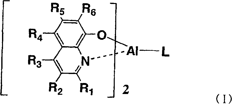
本发明涉及有机电致发光器件,该有机电致发光器件通过在基板上层叠阳极、包含空穴传输层、发光层和电子传输层的有机层以及阴极而形成,在发光层与阳极之间具有空穴传输层,在发光层与阴极之间具有电子传输层,其特征在于:在发光层中,含有下述通式(I)所示的有机金属络合物作为主体材料,并且含有通式(II)所示的有机金属络合物作为客体材料。The present invention relates to an organic electroluminescent device formed by laminating an anode, an organic layer including a hole transport layer, a light emitting layer, and an electron transport layer, and a cathode on a substrate, with an The hole transport layer has an electron transport layer between the light-emitting layer and the cathode, and is characterized in that: the light-emitting layer contains an organometallic complex represented by the following general formula (I) as a host material, and contains the general formula The organometallic complex shown in (II) was used as the guest material.
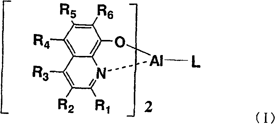
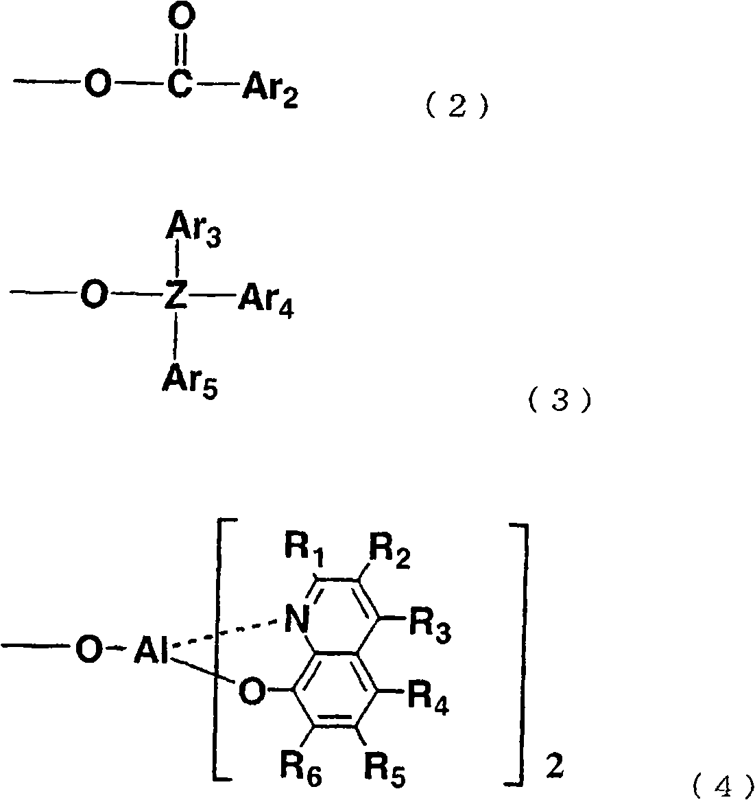
式中,R1~R6各自独立地表示氢原子、烷基、芳烷基、链烯基、氰基、烷氧基、可以具有取代基的芳香族烃基或可以具有取代基的芳香族杂环基。L表示下述通式(1)、(2)、(3)或(4)所示的1价基团:In the formula, R 1 to R 6 each independently represent a hydrogen atom, an alkyl group, an aralkyl group, an alkenyl group, a cyano group, an alkoxy group, an aromatic hydrocarbon group that may have a substituent, or an aromatic heterohydrocarbon group that may have a substituent. Ring base. L represents a monovalent group represented by the following general formula (1), (2), (3) or (4):
-O-Ar1 (1)-O-Ar 1 (1)

Ar1~Ar5各自独立地表示可以具有取代基的芳香族烃环基或可以具有取代基的芳香族杂环基,Z表示硅或锗,R1~R6具有与通式(I)相同的含义。Ar 1 to Ar 5 each independently represent an optionally substituted aromatic hydrocarbon ring group or an optionally substituted aromatic heterocyclic group, Z represents silicon or germanium, and R 1 to R 6 have the same formula (I) meaning.

式中,R7~R14各自独立地表示氢原子、烷基、芳烷基、链烯基、氰基、烷氧基、可以具有取代基的芳香族烃基或可以具有取代基的芳香族杂环基。In the formula, R 7 to R 14 each independently represent a hydrogen atom, an alkyl group, an aralkyl group, an alkenyl group, a cyano group, an alkoxy group, an optionally substituted aromatic hydrocarbon group or an optionally substituted aromatic hetero Ring base.
本发明的有机EL器件涉及发光层中含有上述通式(I)所示的有机金属络合物(也称为Al络合物)化合物和上述通式(II)所示的有机金属络合物(也称为Ir络合物)的所谓利用了磷光的有机EL器件。使用通式(I)所示的Al络合物作为主体材料,而且使用通式(II)所示的Ir络合物作为磷光性客体材料。The organic EL device of the present invention relates to an organic metal complex compound (also called an Al complex) compound represented by the above general formula (I) and an organic metal complex compound represented by the above general formula (II) in the light-emitting layer. (also referred to as Ir complex) so-called organic EL devices utilizing phosphorescence. An Al complex represented by general formula (I) is used as a host material, and an Ir complex represented by general formula (II) is used as a phosphorescent guest material.
其中,所谓主体材料,是指形成该层的材料中占50重量%以上的成分,所谓客体材料,是指形成该层的材料中占不足50重量%的成分。本发明的有机EL器件中,发光层中含有的Al络合物具有比该层中含有的磷光性Ir络合物的激发三重态能级更高的能量状态的激发三重态能级在基本上是必要的。Here, the host material refers to a component that accounts for more than 50% by weight of the material forming the layer, and the so-called guest material refers to a component that accounts for less than 50% by weight of the material forming the layer. In the organic EL device of the present invention, the excited triplet energy level of the Al complex contained in the light-emitting layer has an energy state higher than the excited triplet energy level of the phosphorescent Ir complex contained in the layer is substantially necessary.
此外,希望是能够提供稳定的薄膜形状,具有高Tg,高效传输空穴和/或电子的化合物。此外,还要求是电化学且化学上稳定,在制造时或使用时难以产生形成阱或消除发光的杂质的化合物。为了使磷光性有机络合物的发光不易受到空穴传输层的激发三重态能级的影响,因此具有确保发光区域与空穴传输层界面有适度距离的空穴注入能力也是重要的。In addition, compounds that can provide stable thin film shapes, have high Tg, and transport holes and/or electrons efficiently are desired. In addition, it is also required to be electrochemically and chemically stable, and it is difficult to generate a compound that forms a trap or eliminates an impurity that emits light during production or use. In order to make the light emission of the phosphorescent organic complex less affected by the excited triplet level of the hole transport layer, it is also important to have a hole injection capability that ensures an appropriate distance between the light emitting region and the interface of the hole transport layer.
作为满足这些条件的发光层形成材料,本发明中使用上述通式(I)所示的Al络合物作为主体材料。通式(I)中,R1~R6各自独立地表示氢原子、烷基、芳烷基、链烯基、氰基、烷氧基、可以具有取代基的芳香族烃基或可以具有取代基的芳香族杂环基。作为烷基,优选例示碳原子数为1~6的烷基(以下称为低级烷基),作为芳烷基,优选例示苄基、苯乙基,作为链烯基,优选例示碳原子数为1~6的低级链烯基,作为烷氧基的烷基部,优选例示低级烷基。As a material for forming a light-emitting layer satisfying these conditions, the Al complex represented by the above general formula (I) is used as a host material in the present invention. In the general formula (I), R 1 to R 6 each independently represent a hydrogen atom, an alkyl group, an aralkyl group, an alkenyl group, a cyano group, an alkoxy group, an aromatic hydrocarbon group that may have a substituent, or an optional substituent aromatic heterocyclic group. As an alkyl group, preferably an alkyl group having 1 to 6 carbon atoms (hereinafter referred to as a lower alkyl group), as an aralkyl group, preferably a benzyl group or a phenethyl group, as an alkenyl group, preferably an example having a carbon number of As for the lower alkenyl group of 1 to 6, the lower alkyl group is preferably exemplified as the alkyl portion of the alkoxy group.
此外,作为芳香族烃基,优选例示苯基、萘基、苊基、蒽基等芳香族烃基,作为芳香族杂环基,优选例示吡啶基、喹啉基、噻吩基、咔唑基、吲哚基、呋喃基等芳香族杂环基。当它们为具有取代基的芳香族烃基或芳香族杂环基时,作为取代基,可以列举低级烷基,低级烷氧基,苯氧基、苄氧基、苯基、萘基等。In addition, as an aromatic hydrocarbon group, preferable examples include aromatic hydrocarbon groups such as phenyl, naphthyl, acenaphthyl, and anthracenyl groups, and as an aromatic heterocyclic group, preferable examples include pyridyl, quinolinyl, thienyl, carbazolyl, and indole. Aromatic heterocyclic groups such as radicals and furyls. When they are aromatic hydrocarbon groups or aromatic heterocyclic groups having substituents, examples of substituents include lower alkyl, lower alkoxy, phenoxy, benzyloxy, phenyl, naphthyl and the like.
通式(I)所示的化合物,更优选选择R1~R6为氢原子、低级烷基或低级烷氧基的化合物。As for the compound represented by the general formula (I), it is more preferable to select a compound in which R 1 to R 6 is a hydrogen atom, a lower alkyl group or a lower alkoxy group.
通式(I)中,L表示上述通式(1)、(2)、(3)或(4)所示的基团,Ar1~Ar5各自独立地表示可以具有取代基的芳香族烃基或可以具有取代基的芳香族杂环基,Z表示硅或锗。作为优选的Ar1~Ar2,可以列举苯基、萘基或它们被烷基或芳基取代的芳香族烃基。作为该烷基,优选甲基等低级烷基,作为芳基,优选苯基、萘基或它们被低级烷基取代的基团。作为优选的Ar3~Ar5,可以列举苯基或低级烷基取代的苯基。上述通式(4)的R1~R6具有与上述通式(I)中说明的R1~R6相同的含义。In the general formula (I), L represents a group represented by the above general formula (1), (2), (3) or (4), Ar 1 to Ar 5 each independently represent an aromatic hydrocarbon group which may have a substituent Or an aromatic heterocyclic group which may have a substituent, and Z represents silicon or germanium. Preferable examples of Ar 1 to Ar 2 include phenyl, naphthyl, and aromatic hydrocarbon groups substituted with alkyl or aryl. The alkyl group is preferably a lower alkyl group such as a methyl group, and the aryl group is preferably a phenyl group, a naphthyl group, or a group substituted by a lower alkyl group. Preferable examples of Ar 3 to Ar 5 include phenyl or lower alkyl-substituted phenyl. R 1 to R 6 in the above general formula (4) have the same meanings as R 1 to R 6 described in the above general formula (I).
通式(I)所示的Al络合物通过例如对应的金属盐和式(III)所示的化合物和式(1’)、(2’)或(3’)所示的化合物以2比1的摩尔比进行络合物形成反应而合成。应予说明,式(III)中,R1~R6与通式(I)的R1~R6对应,在式(1’)~(3’)中,Ar1~Ar5和Z对应于通式(I)中的L的Ar1~Ar5和Z。The Al complex compound shown in general formula (I) is by for example corresponding metal salt and the compound shown in formula (III) and the compound shown in formula (1'), (2') or (3') in 2 ratios A molar ratio of 1 was synthesized by complex formation reaction. It should be noted that in formula (III), R 1 to R 6 correspond to R 1 to R 6 in general formula (I), and in formulas (1') to (3'), Ar 1 to Ar 5 correspond to Z Ar 1 to Ar 5 and Z of L in the general formula (I).
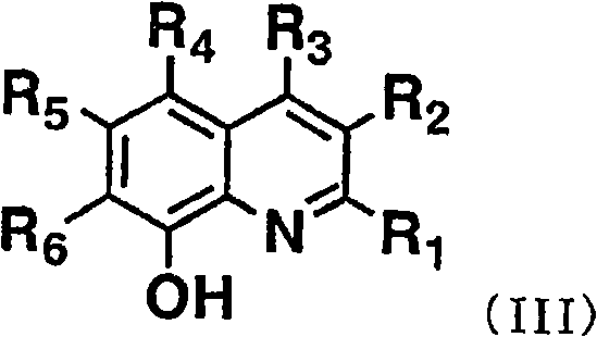
HO-Ar1 HO-Ar 1
(1′)(1')

L为通式(4)所示基团的通式(I)所示的Al络合物,通过对应的金属盐和式(III)所示的化合物之间的络合物形成反应合成。合成反应例如按由Y.Kushi等所示的方法(J.Amer.Chem.Soc.,第92卷,第91页,1970年)进行。The Al complex compound represented by the general formula (I) in which L is a group represented by the general formula (4), is synthesized by a complex forming reaction between the corresponding metal salt and the compound represented by the formula (III). The synthesis reaction is carried out, for example, according to the method shown by Y. Kushi et al. (J. Amer. Chem. Soc., Vol. 92, p. 91, 1970).
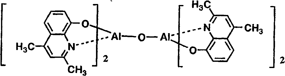
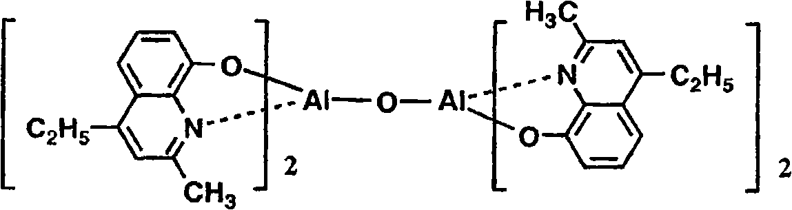
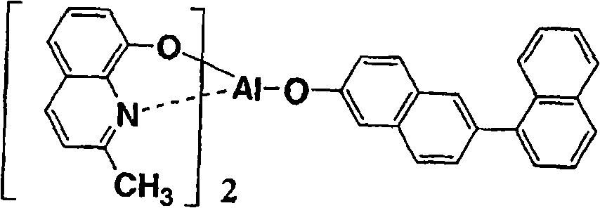
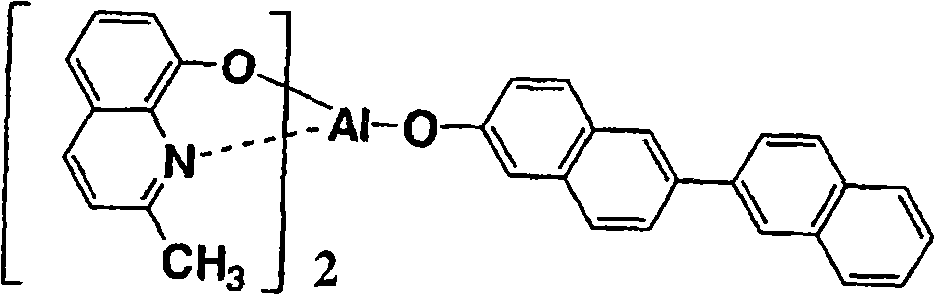
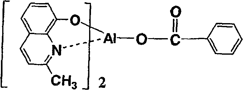
以下例示通式(I)所示的Al络合物,但并不限于下述的化合物。再有,将化合物1简称为BmqAl,将化合物11简称为BAlq。Al complexes represented by the general formula (I) are exemplified below, but are not limited to the following compounds. In addition,

(化合物4) (Compound 4)


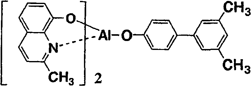


(化合物16) (compound 16)


作为发光层中的客体材料,使用上述通式(II)所示的Ir络合物。As the guest material in the light-emitting layer, an Ir complex represented by the above general formula (II) is used.
通式(II)中,R7~R14各自独立地表示氢原子、烷基、芳烷基、链烯基、氰基、烷氧基、可以具有取代基的芳香族烃基或可以具有取代基的芳香族杂环基。此外,邻接的R7和R8、R8和R9、R9和R10、R11和R12、R12和R13、R13和R14可形成环,这些环可以是芳香环。In the general formula (II), R 7 to R 14 each independently represent a hydrogen atom, an alkyl group, an aralkyl group, an alkenyl group, a cyano group, an alkoxy group, an aromatic hydrocarbon group that may have a substituent, or an optional substituent aromatic heterocyclic group. In addition, adjacent R 7 and R 8 , R 8 and R 9 , R 9 and R 10 , R 11 and R 12 , R 12 and R 13 , R 13 and R 14 may form a ring, and these rings may be aromatic rings.
作为烷基,优选例示碳原子数为1~6的烷基(以下称为低级烷基),作为芳烷基,优选例示苄基、苯乙基,作为链烯基,优选例示碳原子数为1~6的低级链烯基,作为烷氧基的烷基部,优选例示低级烷基。As an alkyl group, preferably an alkyl group having 1 to 6 carbon atoms (hereinafter referred to as a lower alkyl group), as an aralkyl group, preferably a benzyl group or a phenethyl group, as an alkenyl group, preferably an example having a carbon number of As for the lower alkenyl group of 1 to 6, the lower alkyl group is preferably exemplified as the alkyl portion of the alkoxy group.
此外,作为芳香族烃基,优选例示苯基、萘基、苊基、蒽基等,作为芳香族杂环基,优选例示吡啶基、喹啉基、噻吩基、咔唑基、吲哚基、呋喃基等。当它们为具有取代基的芳香族烃基或芳香族杂环基时,作为取代基,可以列举低级烷基,低级烷氧基,苯氧基、苄氧基、苯基、萘基等。In addition, as the aromatic hydrocarbon group, preferably, phenyl, naphthyl, acenaphthyl, anthracenyl, etc. are exemplified, and as the aromatic heterocyclic group, preferably, pyridyl, quinolinyl, thienyl, carbazolyl, indolyl, furanyl, etc. are exemplified. Base etc. When they are aromatic hydrocarbon groups or aromatic heterocyclic groups having substituents, examples of substituents include lower alkyl, lower alkoxy, phenoxy, benzyloxy, phenyl, naphthyl and the like.
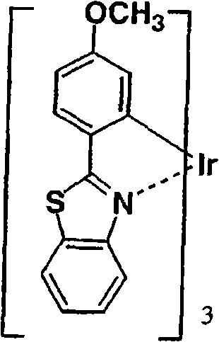
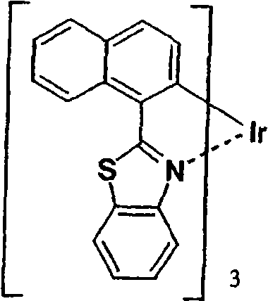
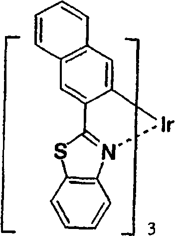
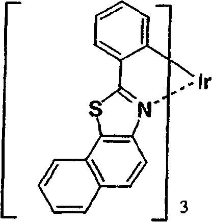
作为更优选的Ir络合物,可以列举Irbt3等。以下示出通式(II)所示的有机金属络合物的具体例,但并不限于下述的化合物。应予说明,将化合物31简称为Irbt3。Irbt3 etc. are mentioned as a more preferable Ir complex. Specific examples of the organometallic complex represented by the general formula (II) are shown below, but are not limited to the following compounds. In addition, compound 31 is abbreviated as Irbt3.


本发明中用于发光层的主体材料能够使电子和空穴大致均等地流过,因此能够在发光层的中央使其发光。因此,不会象TAZ那样在空穴传输侧发光而产生能量向空穴传输层的迁移,导致效率降低,也不会象CPB那样在电子传输层侧发光,使能量向电子传输层迁移从而使效率降低,能够使用作为空穴传输层的α-NPD和作为电子传输层的Alq3这样的可靠性高的材料。The host material used for the light-emitting layer in the present invention allows electrons and holes to flow approximately equally, and thus can cause light to be emitted in the center of the light-emitting layer. Therefore, it will not emit light on the hole transport side like TAZ to generate energy transfer to the hole transport layer, resulting in a decrease in efficiency, nor will it emit light on the electron transport layer side like CPB, so that energy will migrate to the electron transport layer to make Efficiency decreases, and highly reliable materials such as α-NPD as a hole transport layer and Alq3 as an electron transport layer can be used.
附图说明 Description of drawings
图1为表示有机电致发光器件的一例的截面示意图。FIG. 1 is a schematic cross-sectional view showing an example of an organic electroluminescence device.
附图标记的说明Explanation of reference signs
1:基板,2:阳极,3:空穴注入层,4:空穴传输层,5:发光层,6:电子传输层,7:阴极1: substrate, 2: anode, 3: hole injection layer, 4: hole transport layer, 5: light emitting layer, 6: electron transport layer, 7: cathode
具体实施方式 Detailed ways
以下,参照附图对本发明的有机EL器件进行说明。图1为示意地表示本发明中使用的一般有机EL器件的结构例的截面图。本发明的有机EL器件中,具有基板1、阳极2、空穴传输层4、发光层5、电子传输层6及阴极7作为必需层,可以省略必需层以外的层,例如空穴注入层3,另外,必要时可设置其他层。但是,本发明的有机EL器件中,空穴阻挡层是非必要的。由于不设置空穴阻挡层,使层结构得到简化,带来制造上、性能上的优点。Hereinafter, the organic EL device of the present invention will be described with reference to the drawings. FIG. 1 is a cross-sectional view schematically showing a structural example of a general organic EL device used in the present invention. In the organic EL device of the present invention, there are
基板1成为有机电致发光器件的支持体,可以使用石英或玻璃的板、金属板或金属箔、塑料膜或片等。特别优选玻璃板,聚酯、聚甲基丙烯酸酯、聚碳酸酯、聚砜等透明合成树脂的板。当使用合成树脂基板时,必需注意气体阻隔性。如果基板的气体阻隔性过小,则由于透过基板的外部气体导致有机电致发光器件劣化,故不优选。因此,通过在合成树脂基板的至少一个面上设置致密的硅氧化膜等以确保气体阻隔性的方法也是优选的方法之一。The
在基板1上设置有阳极2,阳极起到了向空穴传输层注入空穴的作用。该阳极通常由铝、金、银、镍、钯、铂等金属,铟和/或锡的氧化物等金属氧化物,碘化铜等卤化金属,炭黑,或聚(3-甲基噻吩)、聚吡咯、聚苯胺等导电性高分子等构成。阳极的形成通常大多采用溅射法、真空蒸镀法等进行。此外,在银等金属微粒、碘化铜等微粒、炭黑、导电性的金属氧化物微粒、导电性高分子微粉末等的情形下,也可以通过分散于适当的粘合剂树脂溶液中,涂布在基板1上,形成阳极2。此外,在导电性高分子的情形下,也可以通过电解聚合直接在基板上形成薄膜,或者通过在基板上涂布导电性高分子从而形成阳极。阳极也可以用不同的物质层叠形成。阳极的厚度因所需的透明性而异。当需要透明性时,通常使可见光的透过率为60%以上、优选80%以上,这时,厚度通常为5~1000nm,优选10~500nm左右。当可以为不透明时,阳极2可以与基板1相同。此外,也可以进一步在上述阳极上层合不同的导电材料。An
在阳极2上设置有空穴传输层4。在两者之间也可以设置空穴注入层3。作为空穴传输层的材料所要求的条件,必须是从阳极的空穴注入效率高并且能够高效地传输所注入的空穴的材料。因此,要求离子化电势小,对可见光的透明性高,并且空穴迁移率大,进而稳定性优异,在制造时或使用时难以产生形成阱的杂质。此外,由于与发光层5相接,因此要求不消除从发光层所发出的光,或者在与发光层之间不形成激基复合物从而使效率降低。除了上述一般要求之外,当考虑车载显示的应用时,对于器件还要求具有耐热性。因此,优选Tg具有85℃以上的值的材料。A hole transport layer 4 is arranged on the
本发明的有机EL器件中,作为空穴传输材料,可以使用α-NPD这样的公知的三芳基胺二聚体。In the organic EL device of the present invention, known triarylamine dimers such as α-NPD can be used as the hole transport material.
应予说明,根据需要也可以将公知的化合物作为其他空穴传输材料与三芳基胺二聚体并用。可以列举例如含有2个以上的叔胺且2个以上的稠合芳香环取代于氮原子上的芳香族二胺、4,4’,4”-三(1-萘基苯基氨基)三苯胺等具有星形结构的芳香族胺化合物、三苯胺的四聚体组成的芳香族胺化合物、2,2’,7,7’-四-(二苯基氨基)-9,9′-螺二芴等螺环化合物等。这些化合物可以单独使用,也可以根据需要混合使用。It should be noted that, if necessary, a known compound may be used in combination with the triarylamine dimer as another hole transport material. Examples include aromatic diamines containing two or more tertiary amines and two or more fused aromatic rings substituted on nitrogen atoms, 4,4',4"-tris(1-naphthylphenylamino)triphenylamine Aromatic amine compounds with a star structure, aromatic amine compounds composed of tetramers of triphenylamine, 2,2',7,7'-tetra-(diphenylamino)-9,9'-spirobi Spiral compounds such as fluorene, etc. These compounds may be used alone or in combination as necessary.
此外,除了上述化合物之外,作为空穴传输层的材料,可以举出聚乙烯基咔唑、聚乙烯基三苯胺、含有四苯基联苯胺的聚亚芳基醚砜等高分子材料。In addition to the above-mentioned compounds, polymer materials such as polyvinylcarbazole, polyvinyltriphenylamine, polyarylene ether sulfone containing tetraphenylbenzidine, and the like are exemplified as materials for the hole transport layer.
在用涂布法形成空穴传输层的情况下,添加1种以上空穴传输材料、以及根据需要不会形成空穴的阱的粘合剂树脂、涂布性改善剂等添加剂,通过溶解制备涂布溶液,通过旋转涂布法等方法涂布在阳极2上,通过干燥形成空穴传输层4。作为粘合剂树脂,可以举出聚碳酸酯、聚芳酯、聚酯等。如果粘合剂树脂的添加量多,则使空穴迁移率降低,因此希望其添加量少,通常优选为50重量%以下。In the case of forming the hole transport layer by the coating method, add one or more hole transport materials, and if necessary, additives such as a binder resin that does not form hole traps, a coatability improver, etc., and prepare by dissolving The coating solution is applied on the
在用真空蒸镀法形成的情况下,将空穴传输材料放入设置在真空容器内的坩埚中,用适当的真空泵将真空容器内抽气至10-4Pa左右,然后加热坩埚,使空穴传输材料蒸发,在与坩埚相向设置的形成有阳极的基板上形成空穴传输层4。空穴传输层的膜厚通常为5~300nm,优选为10~100nm。为了均匀地形成如此薄的膜,一般常常使用真空蒸镀法。In the case of forming by the vacuum evaporation method, the hole transport material is placed in a crucible placed in a vacuum container, and the inside of the vacuum container is evacuated to about 10 -4 Pa with an appropriate vacuum pump, and then the crucible is heated to make the air The hole transport material is evaporated, and the hole transport layer 4 is formed on the substrate on which the anode is formed facing the crucible. The film thickness of the hole transport layer is usually 5 to 300 nm, preferably 10 to 100 nm. In order to uniformly form such a thin film, a vacuum evaporation method is generally used.
在空穴传输层4上设置有发光层5。发光层含有通式(I)所示的Al络合物和通式(II)所示的Ir络合物,在提供电场的电极间,通过从阳极注入并移动通过空穴传输层的空穴与从阴极注入并移动通过电子传输层6的电子的再结合而被激发,显示出强发光。应予说明,在不损害本发明的性能的范围内,发光层5可以含有其他主体材料(发挥与通式(I)的络合物相同的作用)或荧光色素等其他成分。A
通式(II)所示的Ir络合物在发光层中的含量优选在0.1~30重量%的范围内。当为0.1重量%以下时,对于器件的发光效率的提高没有帮助,而当超过30重量%时,Ir络合物之间形成2聚体等而引起浓度消光,导致发光效率降低。在现有使用了荧光(单重态)的器件中,倾向于优选比发光层中含有的荧光性色素(掺杂剂)的量稍多。Ir络合物相对于膜厚方向可以部分地包含在发光层中,或者不均匀地分布。发光层5的膜厚通常为10~200nm,优选为20~100nm。采用与空穴传输层同样的方法形成薄膜。The content of the Ir complex represented by the general formula (II) in the light-emitting layer is preferably in the range of 0.1 to 30% by weight. When it is 0.1% by weight or less, it does not contribute to the improvement of the luminous efficiency of the device, and when it exceeds 30% by weight, dimers and the like are formed between Ir complexes to cause concentration extinction, resulting in a decrease in luminous efficiency. In conventional devices using fluorescence (singlet state), it tends to be preferable to have a slightly larger amount of the fluorescent dye (dopant) than that contained in the light emitting layer. The Ir complex may be partially contained in the light-emitting layer with respect to the film thickness direction, or may be non-uniformly distributed. The film thickness of the
为了进一步提高器件的发光效率,在发光层5和阴极7之间设置电子传输层6。电子传输层由能够在施加了电场的电极间高效地将从阴极注入的电子向发光层的方向传输的化合物形成。作为电子传输层6中使用的电子传输性化合物,必须是从阴极7的电子注入效率高且具有高电子迁移率从而能够高效地传输所注入的电子的化合物。In order to further improve the luminous efficiency of the device, an
作为满足这样的条件的电子传输材料,可以举出Alq3等金属络合物、10-羟基苯并[h]喹啉的金属络合物、噁二唑衍生物、二苯乙烯基联苯衍生物、silole衍生物、3-或5-羟基黄酮金属络合物、苯并噁唑金属络合物、苯并噻唑金属络合物、三苯并咪唑基苯、喹喔啉化合物、菲咯啉衍生物、2-叔丁基-9,10-N,N′-二氰基蒽醌二亚胺、n型氢化非晶质碳化硅、n型硫化锌、n型硒化锌等。电子传输层6的膜厚通常为5~200nm,优选为10~100nm。电子传输层与空穴传输层相同,通过采用涂布法或真空蒸镀法层叠于发光层上而形成。通常使用真空蒸镀法。Examples of electron transport materials satisfying such conditions include metal complexes such as Alq3, metal complexes of 10-hydroxybenzo[h]quinoline, oxadiazole derivatives, and distyrylbiphenyl derivatives. , silole derivatives, 3- or 5-hydroxyflavone metal complexes, benzoxazole metal complexes, benzothiazole metal complexes, tribenzimidazolylbenzene, quinoxaline compounds, phenanthroline derivatives substances, 2-tert-butyl-9,10-N,N'-dicyanoanthraquinone diimide, n-type hydrogenated amorphous silicon carbide, n-type zinc sulfide, n-type zinc selenide, etc. The film thickness of the
为了进一步提高空穴注入的效率并且改善整个有机层对阳极的附着力,也可以在空穴传输层4和阳极2之间插入空穴注入层3。通过插入空穴注入层3,具有在初始的器件的驱动电压降低的同时,抑制以恒定电流连续驱动器件时的电压上升的效果。作为用于空穴注入层的材料所要求的条件,要求与阳极的密合性好,能够形成均匀的薄膜,热稳定,即熔点和玻璃化转变温度高,熔点为300℃以上,Tg为100℃以上。另外还可以列举离子化电势低,容易注入来自阳极的空穴,空穴迁移率大。In order to further increase the efficiency of hole injection and improve the adhesion of the entire organic layer to the anode, a hole injection layer 3 may also be inserted between the hole transport layer 4 and the
为了该目的,至今已报道了铜酞菁等酞菁化合物,聚苯胺、聚噻吩等有机化合物,溅射碳膜,以及氧化钒、氧化钌、氧化钼等金属氧化物。对于空穴注入层,也可以按与空穴传输层相同的方式形成薄膜,但无机物的情况下,还可以使用溅射法或电子束蒸镀法、等离子体CVD法。按以上方式形成的阳极缓冲层3的膜厚通常为3~100nm,优选为5~50nm。For this purpose, phthalocyanine compounds such as copper phthalocyanine, organic compounds such as polyaniline and polythiophene, sputtered carbon films, and metal oxides such as vanadium oxide, ruthenium oxide, and molybdenum oxide have been reported so far. The hole injection layer can also be formed into a thin film in the same manner as the hole transport layer, but in the case of an inorganic substance, sputtering, electron beam evaporation, or plasma CVD can also be used. The film thickness of the anode buffer layer 3 formed as described above is usually 3 to 100 nm, preferably 5 to 50 nm.
优选电子传输层6层叠在发光层5之上,在其间不存在空穴阻挡层。It is preferable that the
阴极7起到向发光层5中注入电子的作用。用作阴极的材料,可以使用阳极2中使用的材料,为了高效地进行电子注入,优选功函低的金属,可以使用锡、镁、铟、钙、铝、银等适当的金属或它们的合金。作为具体实例,可以举出镁-银合金、镁-铟合金、铝-锂合金等低功函的合金电极。阴极的膜厚通常与阳极相同。为了保护由低功函金属形成的阴极,通过在它上面进一步层叠功函高且对大气稳定的金属层,增加器件的稳定性。为了该目的,使用铝、银、铜、镍、铬、金、铂等金属。The
进而,在阴极7和电子传输层6之间插入LiF、MgF2、Li2O等极薄绝缘膜(0.1~5nm)作为电子注入层,也是提高器件效率的有效方法。Furthermore, inserting an extremely thin insulating film (0.1-5nm) such as LiF, MgF 2 , Li 2 O, etc. as an electron injection layer between the
应予说明,与图1相反的结构,即在基板1上按照阴极7、电子传输层6、发光层5、空穴传输层4、阳极2的顺序层叠也是可以的,也可以如已述那样在至少一方为高透明性的两片基板间设置本发明的有机EL器件。在此情况下,也可以根据需要追加层或省略层。It should be noted that the structure opposite to that of FIG. 1, that is, the
本发明的有机EL器件能够适用于单一的器件、由阵列状配置的结构组成的器件、阳极与阴极呈X-Y矩阵状配置的结构的任一种。根据本发明的有机EL器件,通过使发光层含有具有特定骨架的化合物及磷光性的金属络合物,可以获得比以往采用来自单重态的发光的器件发光效率更高并且驱动稳定性也得到大大改善的器件,在全色或多色的平板的应用中能够发挥优异的性能The organic EL device of the present invention can be applied to any of a single device, a device composed of a structure arranged in an array, and a structure in which an anode and a cathode are arranged in an X-Y matrix. According to the organic EL device of the present invention, by making the light-emitting layer contain a compound having a specific skeleton and a phosphorescent metal complex, it is possible to obtain higher luminous efficiency than conventional devices using light emission from a singlet state, and drive stability is also improved. Greatly improved device, capable of excellent performance in full-color or multi-color flat panel applications
实施例Example
以下采用合成例和实施例对本发明更详细地进行说明,但只要不超过其主旨,本发明并不限于以下的实施例的记载。Hereinafter, the present invention will be described in more detail using synthesis examples and examples, but the present invention is not limited to the description of the following examples unless the gist is exceeded.
实施例1Example 1
空穴注入层使用铜酞菁(CuPC),空穴传输层使用α-NPD,电子传输层使用Alq3。在形成了由膜厚110nm的ITO形成的阳极的玻璃基板上,采用真空蒸镀法,在真空度5.0×10⁻⁴Pa下层叠各薄膜。首先以

其次,从不同的蒸镀源在空穴传输层上共蒸镀BmqAl(化合物1)和Irbt3(化合物31),形成厚度为47.5nm的发光层。此时,Irbt3的浓度为7.0%。Next, BmqAl (compound 1) and Irbt 3 (compound 31) were co-evaporated on the hole transport layer from different deposition sources to form a light emitting layer with a thickness of 47.5 nm. At this time, the concentration of Irbt 3 was 7.0%.
其次,以


实施例2Example 2
除了从不同的蒸镀源共蒸镀BAlq(化合物11)和Irbt3(化合物31),形成厚度为47.5nm的发光层外,与实施例1同样地制作有机EL器件。应予说明,Irbt3的浓度为7.0%。An organic EL device was produced in the same manner as in Example 1, except that BAlq (compound 11) and Irbt 3 (compound 31) were co-deposited from different deposition sources to form a light emitting layer with a thickness of 47.5 nm. It should be noted that the concentration of Irbt 3 was 7.0%.
比较例1Comparative example 1
除了使用bt2Ir(acac)作为发光层的客体材料以外,与实施例1同样地制作有机EL器件。应予说明,bt2Ir(acac)具有将Irbt3的一个bt置换为acac(乙酰丙酮化物)的结构。An organic EL device was produced in the same manner as in Example 1 except that bt 2 Ir(acac) was used as the guest material of the light-emitting layer. It should be noted that bt 2 Ir(acac) has a structure in which one bt of Irbt 3 is replaced by acac (acetylacetonate).
比较例2Comparative example 2
除了使用bt2Ir(acac)作为发光层的客体材料以外,与实施例2同样地制作有机EL器件。An organic EL device was fabricated in the same manner as in Example 2 except that bt 2 Ir(acac) was used as the guest material of the light-emitting layer.
比较例3Comparative example 3
除了使用BCP作为发光层的主体材料以外,与实施例1同样地制作有机EL器件。An organic EL device was fabricated in the same manner as in Example 1 except that BCP was used as the host material of the light-emitting layer.
比较例4Comparative example 4
除了使用BCP作为发光层的主体材料,使用bt2Ir(acac)作为客体材料以外,与实施例1同样地制作有机EL器件。An organic EL device was produced in the same manner as in Example 1, except that BCP was used as the host material of the light-emitting layer and bt 2 Ir(acac) was used as the guest material.
将实施例和比较例中得到的各个有机EL器件的发光峰值波长、最高发光效率、辉度半衰寿命(初期辉度500cd/m2)示于表1。Table 1 shows the emission peak wavelength, maximum luminous efficiency, and luminance half-life (initial luminance: 500 cd/m 2 ) of each organic EL device obtained in Examples and Comparative Examples.
[表1][Table 1]
根据本发明,能够得到在维持良好的发光特性的情况下,具有长驱动寿命的有机EL器件。因此,可以将本发明的有机EL器件应用于平板显示器(例如OA计算机用或壁挂电视)、车载显示器件、移动电话显示及利用了面发光体的特征的光源(例如复印机光源、液晶显示器及仪表类的背光光源)、显示板、标识灯,其技术价值大。According to the present invention, it is possible to obtain an organic EL device having a long driving life while maintaining good light emission characteristics. Therefore, the organic EL device of the present invention can be applied to flat panel displays (such as OA computer use or wall-mounted TVs), vehicle-mounted display devices, mobile phone displays, and light sources that utilize the characteristics of surface luminous bodies (such as photocopier light sources, liquid crystal displays, and instruments). Class backlight source), display panel, identification light, its technical value is great.
Claims (4)

Applications Claiming Priority (3)
| Application Number | Priority Date | Filing Date | Title |
|---|---|---|---|
| JP2005316223 | 2005-10-31 | ||
| JP316223/2005 | 2005-10-31 | ||
| JP316224/2005 | 2005-10-31 |
Publications (2)
| Publication Number | Publication Date |
|---|---|
| CN101300692A true CN101300692A (en) | 2008-11-05 |
| CN100561768C CN100561768C (en) | 2009-11-18 |
Family
ID=40079646
Family Applications (1)
| Application Number | Title | Priority Date | Filing Date |
|---|---|---|---|
| CNB2006800407577A Expired - Fee Related CN100561768C (en) | 2005-10-31 | 2006-10-10 | Organic Electroluminescent Devices |
Country Status (1)
| Country | Link |
|---|---|
| CN (1) | CN100561768C (en) |
Cited By (2)
| Publication number | Priority date | Publication date | Assignee | Title |
|---|---|---|---|---|
| CN102244204A (en) * | 2011-07-04 | 2011-11-16 | 陕西科技大学 | OLED device and preparation method thereof |
| CN103779498A (en) * | 2014-01-23 | 2014-05-07 | 上海交通大学 | Electron injection method of conductive polymeric materials |
Family Cites Families (1)
| Publication number | Priority date | Publication date | Assignee | Title |
|---|---|---|---|---|
| JP4683829B2 (en) * | 2003-10-17 | 2011-05-18 | 淳二 城戸 | Organic electroluminescent device and manufacturing method thereof |
-
2006
- 2006-10-10 CN CNB2006800407577A patent/CN100561768C/en not_active Expired - Fee Related
Cited By (3)
| Publication number | Priority date | Publication date | Assignee | Title |
|---|---|---|---|---|
| CN102244204A (en) * | 2011-07-04 | 2011-11-16 | 陕西科技大学 | OLED device and preparation method thereof |
| CN102244204B (en) * | 2011-07-04 | 2013-04-10 | 陕西科技大学 | OLED device and preparation method thereof |
| CN103779498A (en) * | 2014-01-23 | 2014-05-07 | 上海交通大学 | Electron injection method of conductive polymeric materials |
Also Published As
| Publication number | Publication date |
|---|---|
| CN100561768C (en) | 2009-11-18 |
Similar Documents
| Publication | Publication Date | Title |
|---|---|---|
| JP4593470B2 (en) | Organic electroluminescence device | |
| JP4545741B2 (en) | Organic electroluminescence device | |
| JP6025959B2 (en) | 2-Azatriphenylene materials for organic light-emitting diodes | |
| JP3855675B2 (en) | Organic electroluminescence device | |
| CN102017218B (en) | Organic electroluminescent element | |
| JP4673744B2 (en) | Organic electroluminescence device | |
| CN102282695B (en) | Organic electroluminescent element | |
| CN101506328B (en) | Organic electroluminescent device material and organic electroluminescent device | |
| JP2005011610A (en) | Organic electroluminescence device | |
| CN103229324B (en) | Organic electroluminescent device | |
| JP2013543864A (en) | Phosphorescent substance | |
| JP5031575B2 (en) | Organic electroluminescence device | |
| JP4864708B2 (en) | Organic electroluminescence device | |
| CN101300692A (en) | Organic Electroluminescent Devices | |
| CN1934907A (en) | Organic electroluminescent element |
Legal Events
| Date | Code | Title | Description |
|---|---|---|---|
| C06 | Publication | ||
| PB01 | Publication | ||
| C10 | Entry into substantive examination | ||
| SE01 | Entry into force of request for substantive examination | ||
| C14 | Grant of patent or utility model | ||
| GR01 | Patent grant | ||
| C56 | Change in the name or address of the patentee |
Owner name: NIPPON STEEL + SUMITOMO METAL CORPORATION Free format text: FORMER NAME: NIPPON SEEL CHEMICAL CO., LTD. |
|
| CP01 | Change in the name or title of a patent holder |
Address after: Tokyo, Japan Patentee after: Nippon Steel Chemical Co. Address before: Tokyo, Japan Patentee before: Nippon Seel Chemical Co., Ltd. |
|
| CF01 | Termination of patent right due to non-payment of annual fee | ||
| CF01 | Termination of patent right due to non-payment of annual fee |
Granted publication date: 20091118 Termination date: 20191010 |