KR101288566B1 - Compound for organic photoelectric device and organic photoelectric device including the same - Google Patents
Compound for organic photoelectric device and organic photoelectric device including the same Download PDFInfo
- Publication number
- KR101288566B1 KR101288566B1 KR1020090125506A KR20090125506A KR101288566B1 KR 101288566 B1 KR101288566 B1 KR 101288566B1 KR 1020090125506 A KR1020090125506 A KR 1020090125506A KR 20090125506 A KR20090125506 A KR 20090125506A KR 101288566 B1 KR101288566 B1 KR 101288566B1
- Authority
- KR
- South Korea
- Prior art keywords
- formula
- compound
- photoelectric device
- group
- organic photoelectric
- Prior art date
- Legal status (The legal status is an assumption and is not a legal conclusion. Google has not performed a legal analysis and makes no representation as to the accuracy of the status listed.)
- Active
Links
- 150000001875 compounds Chemical class 0.000 title claims abstract description 143
- 238000002347 injection Methods 0.000 claims abstract description 33
- 239000007924 injection Substances 0.000 claims abstract description 33
- 239000000463 material Substances 0.000 claims description 43
- 239000010409 thin film Substances 0.000 claims description 26
- -1 stilbenyl group Chemical group 0.000 claims description 23
- 125000000217 alkyl group Chemical group 0.000 claims description 18
- 230000005525 hole transport Effects 0.000 claims description 17
- 238000000034 method Methods 0.000 claims description 16
- 125000003118 aryl group Chemical group 0.000 claims description 13
- 229910052757 nitrogen Inorganic materials 0.000 claims description 12
- 239000002019 doping agent Substances 0.000 claims description 11
- 125000001997 phenyl group Chemical group [H]C1=C([H])C([H])=C(*)C([H])=C1[H] 0.000 claims description 7
- YJTKZCDBKVTVBY-UHFFFAOYSA-N 1,3-Diphenylbenzene Chemical group C1=CC=CC=C1C1=CC=CC(C=2C=CC=CC=2)=C1 YJTKZCDBKVTVBY-UHFFFAOYSA-N 0.000 claims description 5
- 125000002178 anthracenyl group Chemical group C1(=CC=CC2=CC3=CC=CC=C3C=C12)* 0.000 claims description 5
- 125000006267 biphenyl group Chemical group 0.000 claims description 5
- 125000001624 naphthyl group Chemical group 0.000 claims description 5
- 125000001792 phenanthrenyl group Chemical group C1(=CC=CC=2C3=CC=CC=C3C=CC12)* 0.000 claims description 5
- 125000001725 pyrenyl group Chemical group 0.000 claims description 5
- 230000000903 blocking effect Effects 0.000 claims description 4
- 229910052739 hydrogen Inorganic materials 0.000 claims description 3
- 239000001257 hydrogen Substances 0.000 claims description 3
- 125000004435 hydrogen atom Chemical group [H]* 0.000 claims description 3
- IJGRMHOSHXDMSA-UHFFFAOYSA-N Atomic nitrogen Chemical compound N#N IJGRMHOSHXDMSA-UHFFFAOYSA-N 0.000 claims 16
- 229910017464 nitrogen compound Inorganic materials 0.000 claims 6
- 150000002830 nitrogen compounds Chemical class 0.000 claims 6
- QJGQUHMNIGDVPM-UHFFFAOYSA-N nitrogen group Chemical group [N] QJGQUHMNIGDVPM-UHFFFAOYSA-N 0.000 claims 4
- 239000000126 substance Substances 0.000 abstract description 7
- 239000010410 layer Substances 0.000 description 119
- 125000005842 heteroatom Chemical group 0.000 description 39
- 239000007787 solid Substances 0.000 description 37
- WYURNTSHIVDZCO-UHFFFAOYSA-N Tetrahydrofuran Chemical compound C1CCOC1 WYURNTSHIVDZCO-UHFFFAOYSA-N 0.000 description 30
- OKKJLVBELUTLKV-UHFFFAOYSA-N Methanol Chemical compound OC OKKJLVBELUTLKV-UHFFFAOYSA-N 0.000 description 27
- OKTJSMMVPCPJKN-UHFFFAOYSA-N Carbon Chemical group [C] OKTJSMMVPCPJKN-UHFFFAOYSA-N 0.000 description 16
- 230000015572 biosynthetic process Effects 0.000 description 15
- 238000003786 synthesis reaction Methods 0.000 description 15
- YLQBMQCUIZJEEH-UHFFFAOYSA-N tetrahydrofuran Natural products C=1C=COC=1 YLQBMQCUIZJEEH-UHFFFAOYSA-N 0.000 description 15
- 238000006243 chemical reaction Methods 0.000 description 13
- MVPPADPHJFYWMZ-UHFFFAOYSA-N chlorobenzene Chemical compound ClC1=CC=CC=C1 MVPPADPHJFYWMZ-UHFFFAOYSA-N 0.000 description 12
- NFHFRUOZVGFOOS-UHFFFAOYSA-N palladium;triphenylphosphane Chemical compound [Pd].C1=CC=CC=C1P(C=1C=CC=CC=1)C1=CC=CC=C1.C1=CC=CC=C1P(C=1C=CC=CC=1)C1=CC=CC=C1.C1=CC=CC=C1P(C=1C=CC=CC=1)C1=CC=CC=C1.C1=CC=CC=C1P(C=1C=CC=CC=1)C1=CC=CC=C1 NFHFRUOZVGFOOS-UHFFFAOYSA-N 0.000 description 12
- 125000001072 heteroaryl group Chemical group 0.000 description 11
- 125000001424 substituent group Chemical group 0.000 description 10
- 238000001816 cooling Methods 0.000 description 9
- 239000013067 intermediate product Substances 0.000 description 9
- 239000012299 nitrogen atmosphere Substances 0.000 description 9
- BWHMMNNQKKPAPP-UHFFFAOYSA-L potassium carbonate Chemical compound [K+].[K+].[O-]C([O-])=O BWHMMNNQKKPAPP-UHFFFAOYSA-L 0.000 description 9
- 238000010992 reflux Methods 0.000 description 9
- 125000004432 carbon atom Chemical group C* 0.000 description 8
- 239000011368 organic material Substances 0.000 description 8
- XLYOFNOQVPJJNP-UHFFFAOYSA-N water Substances O XLYOFNOQVPJJNP-UHFFFAOYSA-N 0.000 description 7
- UHOVQNZJYSORNB-UHFFFAOYSA-N Benzene Chemical compound C1=CC=CC=C1 UHOVQNZJYSORNB-UHFFFAOYSA-N 0.000 description 6
- HEDRZPFGACZZDS-UHFFFAOYSA-N Chloroform Chemical compound ClC(Cl)Cl HEDRZPFGACZZDS-UHFFFAOYSA-N 0.000 description 6
- KDLHZDBZIXYQEI-UHFFFAOYSA-N Palladium Chemical compound [Pd] KDLHZDBZIXYQEI-UHFFFAOYSA-N 0.000 description 6
- VYPSYNLAJGMNEJ-UHFFFAOYSA-N Silicium dioxide Chemical compound O=[Si]=O VYPSYNLAJGMNEJ-UHFFFAOYSA-N 0.000 description 6
- 238000000921 elemental analysis Methods 0.000 description 6
- 238000005259 measurement Methods 0.000 description 6
- 239000011259 mixed solution Substances 0.000 description 6
- HXITXNWTGFUOAU-UHFFFAOYSA-N phenylboronic acid Chemical compound OB(O)C1=CC=CC=C1 HXITXNWTGFUOAU-UHFFFAOYSA-N 0.000 description 6
- TYJJADVDDVDEDZ-UHFFFAOYSA-M potassium hydrogencarbonate Chemical compound [K+].OC([O-])=O TYJJADVDDVDEDZ-UHFFFAOYSA-M 0.000 description 6
- 239000000376 reactant Substances 0.000 description 6
- 239000000741 silica gel Substances 0.000 description 6
- 229910002027 silica gel Inorganic materials 0.000 description 6
- 239000000243 solution Substances 0.000 description 6
- XLOMVQKBTHCTTD-UHFFFAOYSA-N Zinc monoxide Chemical compound [Zn]=O XLOMVQKBTHCTTD-UHFFFAOYSA-N 0.000 description 4
- 125000000641 acridinyl group Chemical group C1(=CC=CC2=NC3=CC=CC=C3C=C12)* 0.000 description 4
- 229910052799 carbon Inorganic materials 0.000 description 4
- 230000000052 comparative effect Effects 0.000 description 4
- 125000002541 furyl group Chemical group 0.000 description 4
- 125000002883 imidazolyl group Chemical group 0.000 description 4
- 125000004857 imidazopyridinyl group Chemical group N1C(=NC2=C1C=CC=N2)* 0.000 description 4
- 125000002183 isoquinolinyl group Chemical group C1(=NC=CC2=CC=CC=C12)* 0.000 description 4
- 229910052751 metal Inorganic materials 0.000 description 4
- 239000002184 metal Substances 0.000 description 4
- 125000002971 oxazolyl group Chemical group 0.000 description 4
- 125000004076 pyridyl group Chemical group 0.000 description 4
- 125000002943 quinolinyl group Chemical group N1=C(C=CC2=CC=CC=C12)* 0.000 description 4
- 125000000335 thiazolyl group Chemical group 0.000 description 4
- 125000001544 thienyl group Chemical group 0.000 description 4
- 125000001425 triazolyl group Chemical group 0.000 description 4
- KFZMGEQAYNKOFK-UHFFFAOYSA-N Isopropanol Chemical compound CC(C)O KFZMGEQAYNKOFK-UHFFFAOYSA-N 0.000 description 3
- 150000001336 alkenes Chemical class 0.000 description 3
- 150000001345 alkine derivatives Chemical group 0.000 description 3
- 229910052782 aluminium Inorganic materials 0.000 description 3
- XAGFODPZIPBFFR-UHFFFAOYSA-N aluminium Chemical compound [Al] XAGFODPZIPBFFR-UHFFFAOYSA-N 0.000 description 3
- 125000004429 atom Chemical group 0.000 description 3
- 239000011575 calcium Substances 0.000 description 3
- 238000000151 deposition Methods 0.000 description 3
- 238000011161 development Methods 0.000 description 3
- 230000000694 effects Effects 0.000 description 3
- 239000010408 film Substances 0.000 description 3
- 230000005283 ground state Effects 0.000 description 3
- 150000002739 metals Chemical class 0.000 description 3
- 238000002156 mixing Methods 0.000 description 3
- 125000001715 oxadiazolyl group Chemical group 0.000 description 3
- 229910052763 palladium Inorganic materials 0.000 description 3
- 238000010898 silica gel chromatography Methods 0.000 description 3
- 239000002904 solvent Substances 0.000 description 3
- 239000000758 substrate Substances 0.000 description 3
- 238000001771 vacuum deposition Methods 0.000 description 3
- QENGPZGAWFQWCZ-UHFFFAOYSA-N 3-Methylthiophene Chemical compound CC=1C=CSC=1 QENGPZGAWFQWCZ-UHFFFAOYSA-N 0.000 description 2
- PXHVJJICTQNCMI-UHFFFAOYSA-N Nickel Chemical compound [Ni] PXHVJJICTQNCMI-UHFFFAOYSA-N 0.000 description 2
- JUJWROOIHBZHMG-UHFFFAOYSA-N Pyridine Chemical compound C1=CC=NC=C1 JUJWROOIHBZHMG-UHFFFAOYSA-N 0.000 description 2
- YTPLMLYBLZKORZ-UHFFFAOYSA-N Thiophene Chemical compound C=1C=CSC=1 YTPLMLYBLZKORZ-UHFFFAOYSA-N 0.000 description 2
- 239000010405 anode material Substances 0.000 description 2
- 125000004653 anthracenylene group Chemical group 0.000 description 2
- 125000005264 aryl amine group Chemical group 0.000 description 2
- 125000000732 arylene group Chemical group 0.000 description 2
- 125000002529 biphenylenyl group Chemical group C1(=CC=CC=2C3=CC=CC=C3C12)* 0.000 description 2
- 239000011203 carbon fibre reinforced carbon Substances 0.000 description 2
- 239000010406 cathode material Substances 0.000 description 2
- 230000007423 decrease Effects 0.000 description 2
- 230000008021 deposition Effects 0.000 description 2
- 125000001495 ethyl group Chemical group [H]C([H])([H])C([H])([H])* 0.000 description 2
- 238000011156 evaluation Methods 0.000 description 2
- 230000005281 excited state Effects 0.000 description 2
- 125000003983 fluorenyl group Chemical group C1(=CC=CC=2C3=CC=CC=C3CC12)* 0.000 description 2
- 125000005567 fluorenylene group Chemical group 0.000 description 2
- 230000009477 glass transition Effects 0.000 description 2
- 125000005549 heteroarylene group Chemical group 0.000 description 2
- AMGQUBHHOARCQH-UHFFFAOYSA-N indium;oxotin Chemical compound [In].[Sn]=O AMGQUBHHOARCQH-UHFFFAOYSA-N 0.000 description 2
- 125000000959 isobutyl group Chemical group [H]C([H])([H])C([H])(C([H])([H])[H])C([H])([H])* 0.000 description 2
- 125000001449 isopropyl group Chemical group [H]C([H])([H])C([H])(*)C([H])([H])[H] 0.000 description 2
- 125000002496 methyl group Chemical group [H]C([H])([H])* 0.000 description 2
- 125000002950 monocyclic group Chemical group 0.000 description 2
- 125000004957 naphthylene group Chemical group 0.000 description 2
- 239000012044 organic layer Substances 0.000 description 2
- 230000003647 oxidation Effects 0.000 description 2
- 238000007254 oxidation reaction Methods 0.000 description 2
- 125000005560 phenanthrenylene group Chemical group 0.000 description 2
- 125000000843 phenylene group Chemical group C1(=C(C=CC=C1)*)* 0.000 description 2
- BASFCYQUMIYNBI-UHFFFAOYSA-N platinum Chemical compound [Pt] BASFCYQUMIYNBI-UHFFFAOYSA-N 0.000 description 2
- 125000003367 polycyclic group Chemical group 0.000 description 2
- 125000001436 propyl group Chemical group [H]C([*])([H])C([H])([H])C([H])([H])[H] 0.000 description 2
- 125000005548 pyrenylene group Chemical group 0.000 description 2
- 125000002098 pyridazinyl group Chemical group 0.000 description 2
- 150000003413 spiro compounds Chemical class 0.000 description 2
- 125000006836 terphenylene group Chemical group 0.000 description 2
- 125000000999 tert-butyl group Chemical group [H]C([H])([H])C(*)(C([H])([H])[H])C([H])([H])[H] 0.000 description 2
- 239000011787 zinc oxide Substances 0.000 description 2
- SPDPTFAJSFKAMT-UHFFFAOYSA-N 1-n-[4-[4-(n-[4-(3-methyl-n-(3-methylphenyl)anilino)phenyl]anilino)phenyl]phenyl]-4-n,4-n-bis(3-methylphenyl)-1-n-phenylbenzene-1,4-diamine Chemical compound CC1=CC=CC(N(C=2C=CC(=CC=2)N(C=2C=CC=CC=2)C=2C=CC(=CC=2)C=2C=CC(=CC=2)N(C=2C=CC=CC=2)C=2C=CC(=CC=2)N(C=2C=C(C)C=CC=2)C=2C=C(C)C=CC=2)C=2C=C(C)C=CC=2)=C1 SPDPTFAJSFKAMT-UHFFFAOYSA-N 0.000 description 1
- 229910016036 BaF 2 Inorganic materials 0.000 description 1
- OYPRJOBELJOOCE-UHFFFAOYSA-N Calcium Chemical compound [Ca] OYPRJOBELJOOCE-UHFFFAOYSA-N 0.000 description 1
- VYZAMTAEIAYCRO-UHFFFAOYSA-N Chromium Chemical compound [Cr] VYZAMTAEIAYCRO-UHFFFAOYSA-N 0.000 description 1
- 229940126062 Compound A Drugs 0.000 description 1
- RYGMFSIKBFXOCR-UHFFFAOYSA-N Copper Chemical compound [Cu] RYGMFSIKBFXOCR-UHFFFAOYSA-N 0.000 description 1
- 229910052688 Gadolinium Inorganic materials 0.000 description 1
- NLDMNSXOCDLTTB-UHFFFAOYSA-N Heterophylliin A Natural products O1C2COC(=O)C3=CC(O)=C(O)C(O)=C3C3=C(O)C(O)=C(O)C=C3C(=O)OC2C(OC(=O)C=2C=C(O)C(O)=C(O)C=2)C(O)C1OC(=O)C1=CC(O)=C(O)C(O)=C1 NLDMNSXOCDLTTB-UHFFFAOYSA-N 0.000 description 1
- DGAQECJNVWCQMB-PUAWFVPOSA-M Ilexoside XXIX Chemical compound C[C@@H]1CC[C@@]2(CC[C@@]3(C(=CC[C@H]4[C@]3(CC[C@@H]5[C@@]4(CC[C@@H](C5(C)C)OS(=O)(=O)[O-])C)C)[C@@H]2[C@]1(C)O)C)C(=O)O[C@H]6[C@@H]([C@H]([C@@H]([C@H](O6)CO)O)O)O.[Na+] DGAQECJNVWCQMB-PUAWFVPOSA-M 0.000 description 1
- WHXSMMKQMYFTQS-UHFFFAOYSA-N Lithium Chemical compound [Li] WHXSMMKQMYFTQS-UHFFFAOYSA-N 0.000 description 1
- FYYHWMGAXLPEAU-UHFFFAOYSA-N Magnesium Chemical compound [Mg] FYYHWMGAXLPEAU-UHFFFAOYSA-N 0.000 description 1
- CBENFWSGALASAD-UHFFFAOYSA-N Ozone Chemical compound [O-][O+]=O CBENFWSGALASAD-UHFFFAOYSA-N 0.000 description 1
- ZLMJMSJWJFRBEC-UHFFFAOYSA-N Potassium Chemical compound [K] ZLMJMSJWJFRBEC-UHFFFAOYSA-N 0.000 description 1
- BQCADISMDOOEFD-UHFFFAOYSA-N Silver Chemical compound [Ag] BQCADISMDOOEFD-UHFFFAOYSA-N 0.000 description 1
- 229910006404 SnO 2 Inorganic materials 0.000 description 1
- ATJFFYVFTNAWJD-UHFFFAOYSA-N Tin Chemical compound [Sn] ATJFFYVFTNAWJD-UHFFFAOYSA-N 0.000 description 1
- RTAQQCXQSZGOHL-UHFFFAOYSA-N Titanium Chemical compound [Ti] RTAQQCXQSZGOHL-UHFFFAOYSA-N 0.000 description 1
- HCHKCACWOHOZIP-UHFFFAOYSA-N Zinc Chemical compound [Zn] HCHKCACWOHOZIP-UHFFFAOYSA-N 0.000 description 1
- 125000001931 aliphatic group Chemical group 0.000 description 1
- 125000003545 alkoxy group Chemical group 0.000 description 1
- 125000005103 alkyl silyl group Chemical group 0.000 description 1
- 229910045601 alloy Inorganic materials 0.000 description 1
- 239000000956 alloy Substances 0.000 description 1
- XEPMXWGXLQIFJN-UHFFFAOYSA-K aluminum;2-carboxyquinolin-8-olate Chemical compound [Al+3].C1=C(C([O-])=O)N=C2C(O)=CC=CC2=C1.C1=C(C([O-])=O)N=C2C(O)=CC=CC2=C1.C1=C(C([O-])=O)N=C2C(O)=CC=CC2=C1 XEPMXWGXLQIFJN-UHFFFAOYSA-K 0.000 description 1
- 150000004984 aromatic diamines Chemical class 0.000 description 1
- 229910052788 barium Inorganic materials 0.000 description 1
- DSAJWYNOEDNPEQ-UHFFFAOYSA-N barium atom Chemical compound [Ba] DSAJWYNOEDNPEQ-UHFFFAOYSA-N 0.000 description 1
- 239000000872 buffer Substances 0.000 description 1
- 125000004369 butenyl group Chemical group C(=CCC)* 0.000 description 1
- 125000000484 butyl group Chemical group [H]C([*])([H])C([H])([H])C([H])([H])C([H])([H])[H] 0.000 description 1
- 229910052792 caesium Inorganic materials 0.000 description 1
- TVFDJXOCXUVLDH-UHFFFAOYSA-N caesium atom Chemical compound [Cs] TVFDJXOCXUVLDH-UHFFFAOYSA-N 0.000 description 1
- 229910052791 calcium Inorganic materials 0.000 description 1
- 229910052804 chromium Inorganic materials 0.000 description 1
- 239000011651 chromium Substances 0.000 description 1
- 239000011248 coating agent Substances 0.000 description 1
- 238000000576 coating method Methods 0.000 description 1
- JNGZXGGOCLZBFB-IVCQMTBJSA-N compound E Chemical compound N([C@@H](C)C(=O)N[C@@H]1C(N(C)C2=CC=CC=C2C(C=2C=CC=CC=2)=N1)=O)C(=O)CC1=CC(F)=CC(F)=C1 JNGZXGGOCLZBFB-IVCQMTBJSA-N 0.000 description 1
- 229920001940 conductive polymer Polymers 0.000 description 1
- 239000004020 conductor Substances 0.000 description 1
- 229910052802 copper Inorganic materials 0.000 description 1
- 239000010949 copper Substances 0.000 description 1
- 125000004093 cyano group Chemical group *C#N 0.000 description 1
- 125000004122 cyclic group Chemical group 0.000 description 1
- 125000000753 cycloalkyl group Chemical group 0.000 description 1
- 125000001995 cyclobutyl group Chemical group [H]C1([H])C([H])([H])C([H])(*)C1([H])[H] 0.000 description 1
- 125000000113 cyclohexyl group Chemical group [H]C1([H])C([H])([H])C([H])([H])C([H])(*)C([H])([H])C1([H])[H] 0.000 description 1
- 125000001511 cyclopentyl group Chemical group [H]C1([H])C([H])([H])C([H])([H])C([H])(*)C1([H])[H] 0.000 description 1
- 125000001559 cyclopropyl group Chemical group [H]C1([H])C([H])([H])C1([H])* 0.000 description 1
- 150000004985 diamines Chemical class 0.000 description 1
- 238000007598 dipping method Methods 0.000 description 1
- 125000001153 fluoro group Chemical group F* 0.000 description 1
- UIWYJDYFSGRHKR-UHFFFAOYSA-N gadolinium atom Chemical compound [Gd] UIWYJDYFSGRHKR-UHFFFAOYSA-N 0.000 description 1
- 239000011521 glass Substances 0.000 description 1
- PCHJSUWPFVWCPO-UHFFFAOYSA-N gold Chemical compound [Au] PCHJSUWPFVWCPO-UHFFFAOYSA-N 0.000 description 1
- 229910052737 gold Inorganic materials 0.000 description 1
- 239000010931 gold Substances 0.000 description 1
- 125000004051 hexyl group Chemical group [H]C([H])([H])C([H])([H])C([H])([H])C([H])([H])C([H])([H])C([H])([H])* 0.000 description 1
- 229910052738 indium Inorganic materials 0.000 description 1
- APFVFJFRJDLVQX-UHFFFAOYSA-N indium atom Chemical compound [In] APFVFJFRJDLVQX-UHFFFAOYSA-N 0.000 description 1
- 229910003437 indium oxide Inorganic materials 0.000 description 1
- PJXISJQVUVHSOJ-UHFFFAOYSA-N indium(iii) oxide Chemical compound [O-2].[O-2].[O-2].[In+3].[In+3] PJXISJQVUVHSOJ-UHFFFAOYSA-N 0.000 description 1
- 230000009878 intermolecular interaction Effects 0.000 description 1
- 238000007733 ion plating Methods 0.000 description 1
- 125000005647 linker group Chemical group 0.000 description 1
- 229910052744 lithium Inorganic materials 0.000 description 1
- 238000004020 luminiscence type Methods 0.000 description 1
- 229910052749 magnesium Inorganic materials 0.000 description 1
- 239000011777 magnesium Substances 0.000 description 1
- 229910044991 metal oxide Inorganic materials 0.000 description 1
- 150000004706 metal oxides Chemical class 0.000 description 1
- IBHBKWKFFTZAHE-UHFFFAOYSA-N n-[4-[4-(n-naphthalen-1-ylanilino)phenyl]phenyl]-n-phenylnaphthalen-1-amine Chemical compound C1=CC=CC=C1N(C=1C2=CC=CC=C2C=CC=1)C1=CC=C(C=2C=CC(=CC=2)N(C=2C=CC=CC=2)C=2C3=CC=CC=C3C=CC=2)C=C1 IBHBKWKFFTZAHE-UHFFFAOYSA-N 0.000 description 1
- 125000004108 n-butyl group Chemical group [H]C([H])([H])C([H])([H])C([H])([H])C([H])([H])* 0.000 description 1
- 239000007773 negative electrode material Substances 0.000 description 1
- 229910052759 nickel Inorganic materials 0.000 description 1
- 229910052760 oxygen Inorganic materials 0.000 description 1
- 125000001147 pentyl group Chemical group C(CCCC)* 0.000 description 1
- 125000002080 perylenyl group Chemical group C1(=CC=C2C=CC=C3C4=CC=CC5=CC=CC(C1=C23)=C45)* 0.000 description 1
- 229910052698 phosphorus Inorganic materials 0.000 description 1
- 238000007747 plating Methods 0.000 description 1
- 229910052697 platinum Inorganic materials 0.000 description 1
- 229920000767 polyaniline Polymers 0.000 description 1
- 229920000128 polypyrrole Polymers 0.000 description 1
- 239000007774 positive electrode material Substances 0.000 description 1
- 229910052700 potassium Inorganic materials 0.000 description 1
- 239000011591 potassium Substances 0.000 description 1
- 238000002360 preparation method Methods 0.000 description 1
- 125000004368 propenyl group Chemical group C(=CC)* 0.000 description 1
- 125000003373 pyrazinyl group Chemical group 0.000 description 1
- UMJSCPRVCHMLSP-UHFFFAOYSA-N pyridine Natural products COC1=CC=CN=C1 UMJSCPRVCHMLSP-UHFFFAOYSA-N 0.000 description 1
- 238000000197 pyrolysis Methods 0.000 description 1
- 125000000168 pyrrolyl group Chemical group 0.000 description 1
- 238000005215 recombination Methods 0.000 description 1
- 230000006798 recombination Effects 0.000 description 1
- 230000027756 respiratory electron transport chain Effects 0.000 description 1
- 229920006395 saturated elastomer Polymers 0.000 description 1
- 125000002914 sec-butyl group Chemical group [H]C([H])([H])C([H])([H])C([H])(*)C([H])([H])[H] 0.000 description 1
- 239000004065 semiconductor Substances 0.000 description 1
- 229910052709 silver Inorganic materials 0.000 description 1
- 239000004332 silver Substances 0.000 description 1
- 229910052708 sodium Inorganic materials 0.000 description 1
- 239000011734 sodium Substances 0.000 description 1
- 238000004528 spin coating Methods 0.000 description 1
- 238000004544 sputter deposition Methods 0.000 description 1
- 229910052717 sulfur Inorganic materials 0.000 description 1
- 238000005979 thermal decomposition reaction Methods 0.000 description 1
- 229930192474 thiophene Natural products 0.000 description 1
- 229910052718 tin Inorganic materials 0.000 description 1
- 229910052719 titanium Inorganic materials 0.000 description 1
- 239000010936 titanium Substances 0.000 description 1
- 238000012546 transfer Methods 0.000 description 1
- 230000007704 transition Effects 0.000 description 1
- 125000004950 trifluoroalkyl group Chemical group 0.000 description 1
- 125000004417 unsaturated alkyl group Chemical group 0.000 description 1
- 229910052720 vanadium Inorganic materials 0.000 description 1
- GPPXJZIENCGNKB-UHFFFAOYSA-N vanadium Chemical compound [V]#[V] GPPXJZIENCGNKB-UHFFFAOYSA-N 0.000 description 1
- 125000000391 vinyl group Chemical group [H]C([*])=C([H])[H] 0.000 description 1
- 229910052727 yttrium Inorganic materials 0.000 description 1
- VWQVUPCCIRVNHF-UHFFFAOYSA-N yttrium atom Chemical compound [Y] VWQVUPCCIRVNHF-UHFFFAOYSA-N 0.000 description 1
- 229910052725 zinc Inorganic materials 0.000 description 1
- 239000011701 zinc Substances 0.000 description 1
- YVTHLONGBIQYBO-UHFFFAOYSA-N zinc indium(3+) oxygen(2-) Chemical compound [O--].[Zn++].[In+3] YVTHLONGBIQYBO-UHFFFAOYSA-N 0.000 description 1
Images


Classifications
-
- H—ELECTRICITY
- H10—SEMICONDUCTOR DEVICES; ELECTRIC SOLID-STATE DEVICES NOT OTHERWISE PROVIDED FOR
- H10K—ORGANIC ELECTRIC SOLID-STATE DEVICES
- H10K85/00—Organic materials used in the body or electrodes of devices covered by this subclass
- H10K85/60—Organic compounds having low molecular weight
- H10K85/649—Aromatic compounds comprising a hetero atom
- H10K85/654—Aromatic compounds comprising a hetero atom comprising only nitrogen as heteroatom
-
- C—CHEMISTRY; METALLURGY
- C09—DYES; PAINTS; POLISHES; NATURAL RESINS; ADHESIVES; COMPOSITIONS NOT OTHERWISE PROVIDED FOR; APPLICATIONS OF MATERIALS NOT OTHERWISE PROVIDED FOR
- C09K—MATERIALS FOR MISCELLANEOUS APPLICATIONS, NOT PROVIDED FOR ELSEWHERE
- C09K11/00—Luminescent, e.g. electroluminescent, chemiluminescent materials
- C09K11/06—Luminescent, e.g. electroluminescent, chemiluminescent materials containing organic luminescent materials
-
- C—CHEMISTRY; METALLURGY
- C09—DYES; PAINTS; POLISHES; NATURAL RESINS; ADHESIVES; COMPOSITIONS NOT OTHERWISE PROVIDED FOR; APPLICATIONS OF MATERIALS NOT OTHERWISE PROVIDED FOR
- C09B—ORGANIC DYES OR CLOSELY-RELATED COMPOUNDS FOR PRODUCING DYES, e.g. PIGMENTS; MORDANTS; LAKES
- C09B57/00—Other synthetic dyes of known constitution
-
- H—ELECTRICITY
- H05—ELECTRIC TECHNIQUES NOT OTHERWISE PROVIDED FOR
- H05B—ELECTRIC HEATING; ELECTRIC LIGHT SOURCES NOT OTHERWISE PROVIDED FOR; CIRCUIT ARRANGEMENTS FOR ELECTRIC LIGHT SOURCES, IN GENERAL
- H05B33/00—Electroluminescent light sources
- H05B33/10—Apparatus or processes specially adapted to the manufacture of electroluminescent light sources
-
- H—ELECTRICITY
- H10—SEMICONDUCTOR DEVICES; ELECTRIC SOLID-STATE DEVICES NOT OTHERWISE PROVIDED FOR
- H10K—ORGANIC ELECTRIC SOLID-STATE DEVICES
- H10K50/00—Organic light-emitting devices
-
- C—CHEMISTRY; METALLURGY
- C09—DYES; PAINTS; POLISHES; NATURAL RESINS; ADHESIVES; COMPOSITIONS NOT OTHERWISE PROVIDED FOR; APPLICATIONS OF MATERIALS NOT OTHERWISE PROVIDED FOR
- C09K—MATERIALS FOR MISCELLANEOUS APPLICATIONS, NOT PROVIDED FOR ELSEWHERE
- C09K2211/00—Chemical nature of organic luminescent or tenebrescent compounds
- C09K2211/10—Non-macromolecular compounds
- C09K2211/1003—Carbocyclic compounds
- C09K2211/1007—Non-condensed systems
-
- C—CHEMISTRY; METALLURGY
- C09—DYES; PAINTS; POLISHES; NATURAL RESINS; ADHESIVES; COMPOSITIONS NOT OTHERWISE PROVIDED FOR; APPLICATIONS OF MATERIALS NOT OTHERWISE PROVIDED FOR
- C09K—MATERIALS FOR MISCELLANEOUS APPLICATIONS, NOT PROVIDED FOR ELSEWHERE
- C09K2211/00—Chemical nature of organic luminescent or tenebrescent compounds
- C09K2211/10—Non-macromolecular compounds
- C09K2211/1003—Carbocyclic compounds
- C09K2211/1011—Condensed systems
-
- C—CHEMISTRY; METALLURGY
- C09—DYES; PAINTS; POLISHES; NATURAL RESINS; ADHESIVES; COMPOSITIONS NOT OTHERWISE PROVIDED FOR; APPLICATIONS OF MATERIALS NOT OTHERWISE PROVIDED FOR
- C09K—MATERIALS FOR MISCELLANEOUS APPLICATIONS, NOT PROVIDED FOR ELSEWHERE
- C09K2211/00—Chemical nature of organic luminescent or tenebrescent compounds
- C09K2211/10—Non-macromolecular compounds
- C09K2211/1018—Heterocyclic compounds
- C09K2211/1025—Heterocyclic compounds characterised by ligands
- C09K2211/1029—Heterocyclic compounds characterised by ligands containing one nitrogen atom as the heteroatom
-
- C—CHEMISTRY; METALLURGY
- C09—DYES; PAINTS; POLISHES; NATURAL RESINS; ADHESIVES; COMPOSITIONS NOT OTHERWISE PROVIDED FOR; APPLICATIONS OF MATERIALS NOT OTHERWISE PROVIDED FOR
- C09K—MATERIALS FOR MISCELLANEOUS APPLICATIONS, NOT PROVIDED FOR ELSEWHERE
- C09K2211/00—Chemical nature of organic luminescent or tenebrescent compounds
- C09K2211/10—Non-macromolecular compounds
- C09K2211/1018—Heterocyclic compounds
- C09K2211/1025—Heterocyclic compounds characterised by ligands
- C09K2211/1044—Heterocyclic compounds characterised by ligands containing two nitrogen atoms as heteroatoms
-
- C—CHEMISTRY; METALLURGY
- C09—DYES; PAINTS; POLISHES; NATURAL RESINS; ADHESIVES; COMPOSITIONS NOT OTHERWISE PROVIDED FOR; APPLICATIONS OF MATERIALS NOT OTHERWISE PROVIDED FOR
- C09K—MATERIALS FOR MISCELLANEOUS APPLICATIONS, NOT PROVIDED FOR ELSEWHERE
- C09K2211/00—Chemical nature of organic luminescent or tenebrescent compounds
- C09K2211/10—Non-macromolecular compounds
- C09K2211/1018—Heterocyclic compounds
- C09K2211/1025—Heterocyclic compounds characterised by ligands
- C09K2211/1059—Heterocyclic compounds characterised by ligands containing three nitrogen atoms as heteroatoms
-
- Y—GENERAL TAGGING OF NEW TECHNOLOGICAL DEVELOPMENTS; GENERAL TAGGING OF CROSS-SECTIONAL TECHNOLOGIES SPANNING OVER SEVERAL SECTIONS OF THE IPC; TECHNICAL SUBJECTS COVERED BY FORMER USPC CROSS-REFERENCE ART COLLECTIONS [XRACs] AND DIGESTS
- Y02—TECHNOLOGIES OR APPLICATIONS FOR MITIGATION OR ADAPTATION AGAINST CLIMATE CHANGE
- Y02E—REDUCTION OF GREENHOUSE GAS [GHG] EMISSIONS, RELATED TO ENERGY GENERATION, TRANSMISSION OR DISTRIBUTION
- Y02E10/00—Energy generation through renewable energy sources
- Y02E10/50—Photovoltaic [PV] energy
- Y02E10/549—Organic PV cells
Landscapes
- Chemical & Material Sciences (AREA)
- Engineering & Computer Science (AREA)
- Organic Chemistry (AREA)
- Materials Engineering (AREA)
- Physics & Mathematics (AREA)
- Manufacturing & Machinery (AREA)
- Spectroscopy & Molecular Physics (AREA)
- Optics & Photonics (AREA)
- Electroluminescent Light Sources (AREA)
- Photovoltaic Devices (AREA)
- Plural Heterocyclic Compounds (AREA)
- Light Receiving Elements (AREA)
Abstract
유기광전소자용 화합물 및 이를 포함하는 유기광전소자에 관한 것으로, 상기 유기광전소자용 화합물은 하기 화학식 1 또는 2로 표시되는 것을 제공한다.The present invention relates to a compound for an organic photoelectric device and an organic photoelectric device including the same. The compound for an organic photoelectric device provides a compound represented by Chemical Formula 1 or 2 below.
[화학식 1] [화학식 2][Formula 1] [Formula 2]


상기 화학식 1에서 X1 내지 X9 및 Ar1 내지 Ar18의 정의는 명세서에 기재된 바와 같다. 상기 유기광전소자용 화합물을 이용하면, 열적/전기화학적 안정성 및 수명, 효율이 우수한 유기광전소자를 제공할 수 있다.In Formula 1, X1 to X9 and Ar1 to Ar18 are as defined in the specification. By using the compound for an organic photoelectric device, it is possible to provide an organic photoelectric device having excellent thermal / electrochemical stability, lifetime, and efficiency.
유기광전소자, 발광, 전자수송, 전자주입, 열적 안정성, 수명, 효율 Organic photoelectric device, light emission, electron transport, electron injection, thermal stability, lifetime, efficiency
Description
수명, 효율, 전기화학적 안정성 및 열적 안정성이 우수한 유기광전소자를 제공할 수 있는 유기광전소자용 화합물 및 이를 포함하는 유기광전소자에 관한 것이다.The present invention relates to a compound for an organic photoelectric device and an organic photoelectric device including the same, which can provide an organic photoelectric device having excellent lifetime, efficiency, electrochemical stability, and thermal stability.
유기 광전 소자(organic photoelectric device)라 함은 정공 또는 전자를 이용한 전극과 유기물 사이에서의 전하 교류를 필요로 하는 소자를 의미한다.An organic photoelectric device refers to a device that requires charge exchange between an electrode and an organic material using holes or electrons.
유기 광전 소자는 동작 원리에 따라 하기와 같이 크게 두 가지로 나눌 수 있다. 첫째는 외부의 광원으로부터 소자로 유입된 광자에 의하여 유기물층에서 엑시톤(exciton)이 형성되고 이 엑시톤이 전자와 정공으로 분리되고, 이 전자와 정공이 각각 다른 전극으로 전달되어 전류원(전압원)으로 사용되는 형태의 전자소자이다.The organic photoelectric device may be classified into two types according to the operation principle. First, an exciton is formed in an organic material layer by a photon introduced into an element from an external light source. The exciton is separated into an electron and a hole, and the electrons and holes are transferred to different electrodes to be used as a current source Type electronic device.
둘째는 2 개 이상의 전극에 전압 또는 전류를 가하여 전극과 계면을 이루는 유기물 반도체에 정공 또는 전자를 주입하고, 주입된 전자와 정공에 의하여 동작하는 형태의 전자소자이다.The second type is an electronic device in which holes or electrons are injected into an organic semiconductor forming an interface with an electrode by applying a voltage or current to two or more electrodes and operated by injected electrons and holes.
유기 광전 소자의 예로는 유기광전소자, 유기태양전지, 유기 감광체 드럼(organic photo conductor drum), 유기 트랜지스터 등이 있으며, 이들은 모두 소자의 구동을 위하여 정공의 주입 또는 수송 물질, 전자의 주입 또는 수송 물질, 또는 발광 물질을 필요로 한다.Examples of the organic photoelectric device include an organic photoelectric device, an organic solar cell, an organic photo conductor drum, and an organic transistor, all of which are used to inject or transport holes, or inject or transport materials for driving the device. Or a luminescent material.
특히, 유기광전소자(organic light emitting diodes, OLED)는 최근 평판 디스플레이(flat panel display)의 수요가 증가함에 따라 주목받고 있다. 일반적으로 유기 발광 현상이란 유기 물질을 이용하여 전기에너지를 빛에너지로 전환시켜주는 현상을 말한다.In particular, organic light emitting diodes (OLEDs) are attracting attention as the demand for flat panel displays increases. In general, organic light emission phenomenon refers to a phenomenon in which an organic material is used to convert electric energy into light energy.
이러한 유기광전소자는 유기발광재료에 전류를 가하여 전기에너지를 빛으로 전환시키는 소자로서 통상 양극(anode)과 음극(cathode) 사이에 기능성 유기물 층이 삽입된 구조로 이루어져 있다. 여기서 유기물층은 유기광전소자의 효율과 안정성을 높이기 위하여 각기 다른 물질로 구성된 다층의 구조로 이루어진 경우가 많으며, 예컨대 정공주입층, 정공수송층, 발광층, 전자수송층, 전자주입층 등으로 이루어질 수 있다.Such an organic photoelectric device is a device that converts electrical energy into light by applying a current to an organic light emitting material and has a structure in which a functional organic material layer is inserted between an anode and a cathode. The organic layer is often made of a multi-layered structure composed of different materials to increase the efficiency and stability of the organic photoelectric device, for example, it may be made of a hole injection layer, a hole transport layer, a light emitting layer, an electron transport layer, an electron injection layer.
이러한 유기광전소자의 구조에서 두 전극 사이에 전압을 걸어주게 되면 양극에서는 정공(hole)이, 음극에서는 전자(electron)가 유기물층에 주입되게 되고, 주입된 정공과 전자가 만나 재결합(recombination)에 의해 에너지가 높은 여기자를 형성하게 된다. 이때 형성된 여기자가 다시 바닥상태(ground state)로 이동하면서 특정한 파장을 갖는 빛이 발생하게 된다.When the voltage is applied between the two electrodes in the structure of the organic photoelectric device, holes are injected into the organic material layer in the anode and electrons in the cathode, and the injected holes and the electrons meet and recombine by recombination. High energy excitons are formed. At this time, the exciton formed again moves to the ground state, and light having a specific wavelength is generated.
1987년 이스트만 코닥(Eastman Kodak)사에서는 발광층 형성용 재료로서 저분 자인 방향족 디아민과 알루미늄 착물을 이용하고 있는 유기 EL 소자를 처음으로 개발하였고(Appl. Phys. Lett. 51, 913, 1987), 유기 전계 발광 소자에 대해서는 1987년에 C. W. Tang 등이 최초로 실용적인 성능을 가진 소자를 보고하였다 (AppliedPhysics Letters, 51(12), 913-915, 1987년).In 1987, Eastman Kodak developed the first organic EL device using a low molecular weight aromatic diamine and an aluminum complex as a material for forming a light emitting layer (Appl. Phys. Lett. 51, 913, 1987). For the light emitting device, CW Tang et al. Reported the first practical device in 1987 (Applied Physics Letters, 51 (12), 913-915, 1987).
상기 문헌은 유기층으로서 디아민 유도체의 박막(정공 수송층)과 트리스(8-하이드록시-퀴놀레이트)알루미늄(tris(8-hydroxy-quinolate)aluminum, Alq3)의 박막을 적층한 구조를 기재하고 있다.This document describes a structure in which a thin film of a diamine derivative (hole transport layer) and a thin film of tris (8-hydroxy-quinolate) aluminum (Alq 3 ) are laminated as an organic layer.
최근에는, 형광 발광물질뿐 아니라 인광 발광물질도 유기 광전 소자의 발광물질로 사용될 수 있음이 알려졌으며(D. F.O'Brien 등, Applied Physics Letters, 74(3), 442-444, 1999; M. A. Baldo 등, Applied Physics letters, 75(1), 4-6, 1999), 이러한 인광 발광은 바닥상태(ground state)에서 여기상태(excited state)로 전자가 전이한 후, 계간 전이(intersystem crossing)를 통해 단일항 여기자가 삼중항 여기자로 비발광 전이된 다음, 삼중항 여기자가 바닥상태로 전이하면서 발광하는 메카니즘으로 이루어진다.Recently, phosphorescent as well as fluorescent light emitting materials can be used as light emitting materials for organic photoelectric devices (DFO'Brien et al., Applied Physics Letters, 74 (3), 442-444, 1999; MA Baldo et al. , Applied Physics letters, 75 (1), 4-6, 1999), and these phosphorescent luminescences are transferred to the excited state from the ground state to the excited state, and then through intersystem crossing The anti-exciter is non-luminescent transition into triplet excitons, and then the triplet excitons are made to emit light while transitioning to the ground state.
상기한 바와 같이 유기광전소자에서 유기물층으로 사용되는 재료는 기능에 따라, 발광 재료와 전하 수송 재료, 예컨대 정공주입 재료, 정공수송 재료, 전자수송 재료, 전자주입 재료 등으로 분류될 수 있다.As described above, the material used as the organic material layer in the organic photoelectric device may be classified into a light emitting material and a charge transport material, such as a hole injection material, a hole transport material, an electron transport material, an electron injection material, and the like according to a function.
또한, 발광 재료는 발광색에 따라 청색, 녹색, 적색 발광재료와 보다 나은 천연색을 구현하기 위해 필요한 노란색 및 주황색 발광 재료로 구분될 수 있다.Further, the light emitting material can be classified into blue, green, and red light emitting materials and yellow and orange light emitting materials required to realize better natural color depending on the luminescent color.
한편, 발광 재료로서 하나의 물질만 사용하는 경우 분자간 상호 작용에 의하여 최대 발광 파장이 장파장으로 이동하고 색순도가 떨어지거나 발광 감쇄 효과로 소자의 효율이 감소되는 문제가 발생하므로, 색순도의 증가와 에너지 전이를 통한 발광 효율과 안정성을 증가시키기 위하여 발광 재료로서 호스트/도판트 계를 사용할 수 있다.On the other hand, when only one material is used as a light emitting material, there arises a problem that the maximum light emission wavelength shifts to a long wavelength due to intermolecular interaction, the color purity decreases, or the efficiency of the device decreases due to the light emission attenuating effect. A host / dopant system can be used as a light emitting material in order to increase the light emitting efficiency and stability through the light emitting layer.
유기광전소자가 전술한 우수한 특징들을 충분히 발휘하기 위해서는 소자 내 유기물층을 이루는 물질, 예컨대 정공주입 물질, 정공수송 물질, 발광 물질, 전자수송 물질, 전자주입 물질, 발광 재료 중 호스트 및/또는 도판트 등이 안정하고 효율적인 재료에 의하여 뒷받침되는 것이 선행되어야 하며, 아직까지 안정하고 효율적인 유기광전소자용 유기물층 재료의 개발이 충분히 이루어지지 않은 상태이며, 따라서 새로운 재료의 개발이 계속 요구되고 있다. 이와 같은 재료 개발의 필요성은 전술한 다른 유기 광전 소자에서도 마찬가지이다.In order for the organic photoelectric device to fully exhibit the above-mentioned excellent features, a material forming the organic material layer in the device, such as a hole injection material, a hole transport material, a light emitting material, an electron transport material, an electron injection material, a host and / or a dopant in the light emitting material, etc. Supported by this stable and efficient material should be preceded, and development of a stable and efficient organic material layer material for an organic photoelectric device has not been made yet, and therefore, development of new materials is continuously required. The need for such a material development is the same for the other organic photoelectric devices described above.
발광, 또는 전자 주입 및/또는 수송역할을 할 수 있고, 적절한 도펀트와 함께 발광 호스트로서의 역할을 할 수 있는 유기광전소자용 화합물을 제공한다.Provided are a compound for an organic photoelectric device, which may serve as light emitting, or electron injection and / or transport, and may serve as a light emitting host with an appropriate dopant.
수명, 효율, 구동전압, 전기화학적 안정성 및 열적 안정성이 우수한 유기광전소자를 제공하고자 한다.An organic photoelectric device excellent in lifespan, efficiency, driving voltage, electrochemical stability, and thermal stability is provided.
본 발명의 일 측면에서는, 하기 화학식 1 또는 2로 표시되는 유기광전소자용 화합물을 제공한다.In one aspect of the present invention, there is provided a compound for an organic photoelectric device represented by the following formula (1) or (2).
[화학식 1] [화학식 2][Formula 1] [Formula 2]
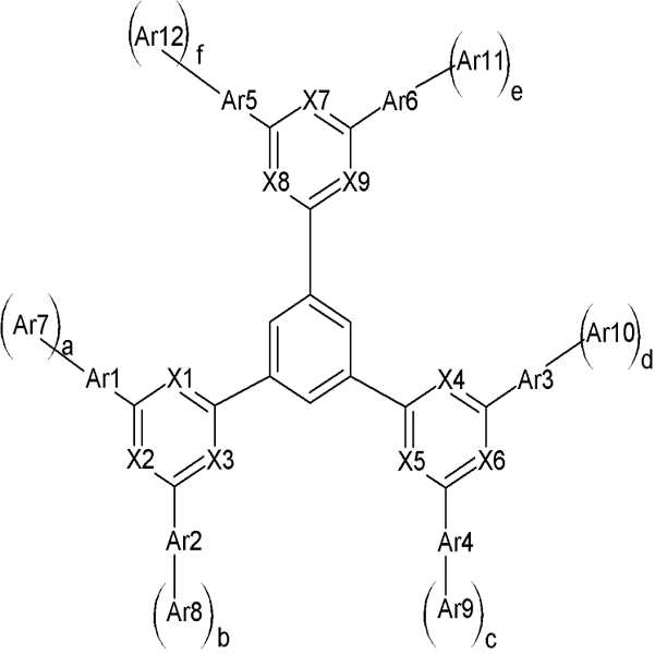

상기 화학식 1 및 2에서, X1 내지 X9는 서로 동일하거나 상이하며, 독립적으로 헤테로원자 또는 C-R이되, 상기 R은 수소, C1 내지 C30 알킬기 및 C6 내지 C30 아릴기로 이루어진 군에서 선택되고, X1 내지 X3 중 적어도 둘은 헤테로원자이며, 상기 X4 내지 X6 중 적어도 하나는 헤테로원자이며, 상기 X7 내지 X9 중 적어도 하 나는 헤테로원자이고, 상기 화학식 1에서, Ar1 내지 Ar6는 서로 동일하거나 상이하며, 독립적으로, 치환 또는 비치환된 C6 내지 C30 아릴렌기, 치환 또는 비치환된 C3 내지 C30 헤테로아릴렌기, 치환 또는 비치환된 C6 내지 C30 아릴아미닐렌기, 치환 또는 비치환된 카바조릴렌기, 및 치환 또는 비치환된 플루오레닐렌기로 이루어진 군에서 선택되고, Ar7 내지 Ar12는 서로 동일하거나 상이하며, 독립적으로 치환 또는 비치환된 C6 내지 C30 아릴기 또는 치환 또는 비치환된 C3 내지 C30 헤테로아릴기리고, a, b, c, d, e 및 f는 서로 동일하거나 상이하며, 독립적으로 1 또는 2의 정수이고, 상기 화학식 2에서, Ar13 내지 Ar18는 서로 동일하거나 상이하며, 독립적으로 치환 또는 비치환된 C6 내지 C30 아릴기, 치환 또는 비치환된 C3 내지 C30 헤테로아릴기, 치환 또는 비치환된 C6 내지 C30 아릴아민기, 치환 또는 비치환된 카바조릴기 및 치환 또는 비치환된 플루오레닐기로 이루어진 군에서 선택된다.In Chemical Formulas 1 and 2, X1 to X9 are the same as or different from each other, and independently heteroatoms or CR, wherein R is selected from the group consisting of hydrogen, C1 to C30 alkyl group, and C6 to C30 aryl group, and among X1 to X3 At least two are heteroatoms, at least one of X4 to X6 is a heteroatom, at least one of X7 to X9 is a heteroatom, and in Formula 1, Ar1 to Ar6 are the same as or different from each other, and are independently substituted Or an unsubstituted C6 to C30 arylene group, a substituted or unsubstituted C3 to C30 heteroarylene group, a substituted or unsubstituted C6 to C30 arylaminilene group, a substituted or unsubstituted carbazoylene group, and a substituted or unsubstituted Selected from the group consisting of fluorenylene groups, Ar7 to Ar12 are the same as or different from each other, and independently substituted or unsubstituted C6 to C30 aryl groups or substituted or Is an unsubstituted C3 to C30 heteroaryl group, a, b, c, d, e and f are the same as or different from each other, independently an integer of 1 or 2, in Formula 2, Ar13 to Ar18 are the same as each other Different, independently substituted or unsubstituted C6 to C30 aryl group, substituted or unsubstituted C3 to C30 heteroaryl group, substituted or unsubstituted C6 to C30 arylamine group, substituted or unsubstituted carbazoyl group and substituted Or an unsubstituted fluorenyl group.
일 실시예에 따르면, 상기 X4 내지 X6 의 헤테로원자의 수는 2일 수 있다.According to one embodiment, the number of heteroatoms of X4 to X6 may be 2.
일 실시예에 따르면, 상기 화학식 1 또는 2로 표시되는 유기광전소자용 화합물은, 상기 X2, X3, X5, X6 및 X7이 헤테로원자인 화합물 또는, 상기 X2, X3, X5, X6 및 X9가 헤테로원자인 화합물일 수 있다.According to one embodiment, the compound for an organic photoelectric device represented by Formula 1 or 2, wherein X2, X3, X5, X6 and X7 is a heteroatom, or X2, X3, X5, X6 and X9 is hetero It may be a compound that is an atom.
일 실시예에 따르면, 상기 화학식 1 또는 2로 표시되는 유기광전소자용 화합물은, 상기 X2, X3, X5, X6, X7 및 X9가 헤테로원자인 화합물; 상기 X2, X3, X5, X6, X8 및 X9가 헤테로원자인 화합물; 상기 X1, X3, X4, X5, X8 및 X9가 헤테로원자인 화합물; 및 상기 X1, X3, X4, X5, X7 및 X9가 헤테로원자 화합물로 이루어진 군에서 선택되는 화합물일 수 있다.According to one embodiment, the compound for an organic photoelectric device represented by Formula 1 or 2, the compound X2, X3, X5, X6, X7 and X9 are heteroatoms; X 2, X 3, X 5, X 6, X 8 and X 9 are heteroatoms; The compound wherein X1, X3, X4, X5, X8 and X9 are heteroatoms; And X1, X3, X4, X5, X7 and X9 may be a compound selected from the group consisting of a heteroatom compound.
일 실시예에 따르면, 상기 화학식 1 또는 2로 표시되는 유기광전소자용 화합물은, 상기 X2, X6, X7 및 X9가 헤테로원자인 화합물 또는, 상기 X3, X5, X7 및 X9가 헤테로원자인 화합물일 수 있다.According to one embodiment, the compound for an organic photoelectric device represented by Formula 1 or 2 is a compound wherein X2, X6, X7 and X9 is a heteroatom, or the compound X3, X5, X7 and X9 is a heteroatom Can be.
일 실시예에 따르면, 상기 화학식 1 또는 2로 표시되는 유기광전소자용 화합물은, 상기 X2, X6, X7, X8 및 X9가 헤테로원자인 화합물 또는, 상기 X3, X5, X7, X8 및 X9가 헤테로원자인 화합물일 수 있다.According to one embodiment, the compound for an organic photoelectric device represented by Formula 1 or 2, wherein X2, X6, X7, X8 and X9 is a heteroatom or X3, X5, X7, X8 and X9 is hetero It may be a compound that is an atom.
일 실시예에 따르면, 상기 화학식 1 또는 2로 표시되는 유기광전소자용 화합물은, 상기 X2, X3, X5, X6, X7, X8 및 X9가 헤테로원자인 화합물 또는, 상기 X1, X3, X4, X5, X7, X8 및 X9가 헤테로원자인 화합물일 수 있다.According to one embodiment, the compound for an organic photoelectric device represented by Formula 1 or 2, wherein X2, X3, X5, X6, X7, X8 and X9 is a heteroatom, or the X1, X3, X4, X5 , X7, X8 and X9 may be a heteroatom.
일 실시예에 따르면, 상기 화학식 1에서, Ar7 내지 Ar12는 서로 동일하거나 상이하며, 독립적으로 페닐기, 비페닐기, 터페닐기, 스틸베닐기, 나프틸기, 안트라세닐기, 페난트레닐기, 파이레닐기 및 페릴레닐기로 이루어진 군에서 선택되고, Ar1 내지 Ar6는 서로 동일하거나 상이하며, 독립적으로 페닐렌기, 비페닐렌기, 터페닐렌기, 스틸베닐렌기, 나프틸렌기, 안트라세닐렌기, 페난트레닐렌기, 파이레닐렌기 및 페릴레닐렌기로 이루어진 군에서 선택되고, 상기 화학식 2에서, Ar13 내지 Ar18은 서로 동일하거나 상이하며, 독립적으로 페닐기, 비페닐기, 터페닐기, 스틸베닐기, 나프틸기, 안트라세닐기, 페난트레닐기, 파이레닐기 및 페릴레닐기로 이루어진 군에서 선택될 수 있다.According to an embodiment, in Formula 1, Ar7 to Ar12 are the same as or different from each other, and independently a phenyl group, a biphenyl group, a terphenyl group, stilbenyl group, naphthyl group, anthracenyl group, phenanthrenyl group, pyrenyl group and Selected from the group consisting of a perylene group, Ar1 to Ar6 are the same as or different from each other, and independently a phenylene group, a biphenylene group, a terphenylene group, a stilbenylene group, a naphthylene group, an anthracenylene group, a phenanthrenylene group, Selected from the group consisting of a pyrenylene group and a peryleneylene group, in Formula 2, Ar13 to Ar18 are the same as or different from each other, and independently a phenyl group, a biphenyl group, a terphenyl group, a stilbenyl group, a naphthyl group, an anthracenyl group, It may be selected from the group consisting of a phenanthrenyl group, a pyrenyl group and a perrylenyl group.
일 실시예에 따르면, 상기 화학식 1에서, Ar7 내지 Ar12는 서로 동일하거나 상이하며, 독립적으로 티오페닐기, 퓨라닐기, 피롤일기, 이미다졸릴기, 티아졸릴 기, 옥사졸릴기, 옥사디아졸릴기, 트리아졸릴기, 피리디닐기, 피라다지닐기, 퀴놀리닐기, 이소퀴놀리닐기, 아크리디닐기, 이미다조피리디닐기, 이미다조피리미디닐기, 벤조퀴놀리닐기 및 페난트롤리디닐기로 이루어진 군에서 선택되고, 상기 화학식 2에서, Ar13 내지 Ar18은 서로 동일하거나 상이하며, 독립적으로 티오페닐기, 퓨라닐기, 피롤일기, 이미다졸릴기, 티아졸릴기, 옥사졸릴기, 옥사디아졸릴기, 트리아졸릴기, 피리디닐기, 피라다지닐기, 퀴놀리닐기, 이소퀴놀리닐기, 아크리디닐기, 이미다조피리디닐기, 이미다조피리미디닐기, 벤조퀴놀리닐기 및 페난트롤리디닐기로 이루어진 군에서 선택될 수 있다.According to one embodiment, in Formula 1, Ar7 to Ar12 are the same as or different from each other, and independently a thiophenyl group, furanyl group, pyrroyl group, imidazolyl group, thiazolyl group, oxazolyl group, oxdiazolyl group, In the group consisting of a triazolyl group, pyridinyl group, pyridazinyl group, quinolinyl group, isoquinolinyl group, acridinyl group, imidazopyridinyl group, imidazopyrimidinyl group, benzoquinolinyl group and phenanthrolidinyl group In Formula 2, Ar13 to Ar18 are the same as or different from each other, and are independently a thiophenyl group, furanyl group, pyrroyl group, imidazolyl group, thiazolyl group, oxazolyl group, oxadiazolyl group, and triazolyl group , Pyridinyl, pyridazinyl, quinolinyl, isoquinolinyl, acridinyl, imidazopyridinyl, imidazopyrimidinyl, benzoquinolinyl and phenanthrolidinyl groups .
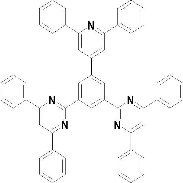
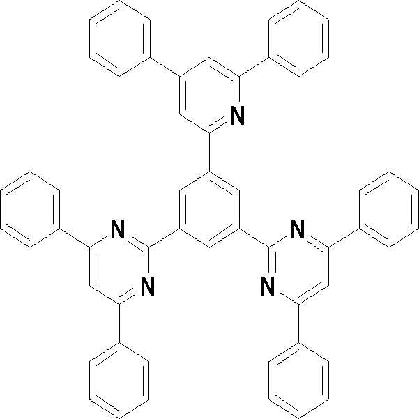
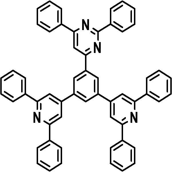
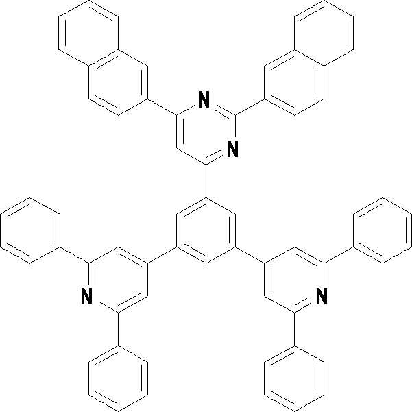
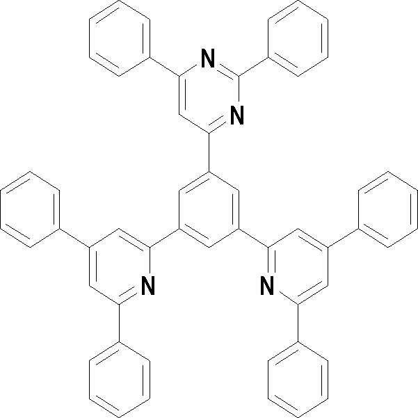
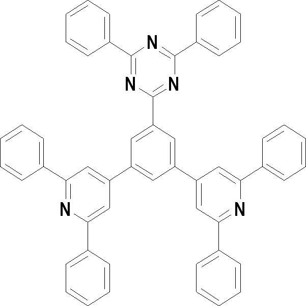
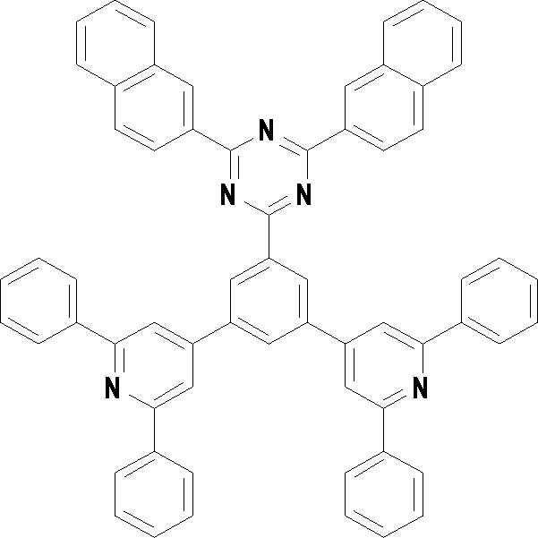
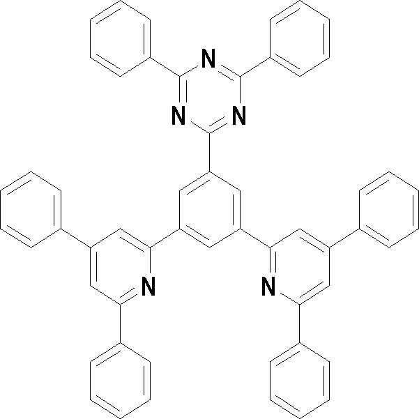
본 발명의 다른 측면에서는, 하기 화학식 3 내지 33 중 어느 하나로 표시되는 유기광전소자용 화합물을 제공한다.In another aspect of the present invention, a compound for an organic photoelectric device represented by one of the following Chemical Formulas 3 to 33 is provided.
[화학식 3] [화학식 4][Formula 3] [Formula 4]


[화학식 5] [화학식 6][Formula 5] [Formula 6]
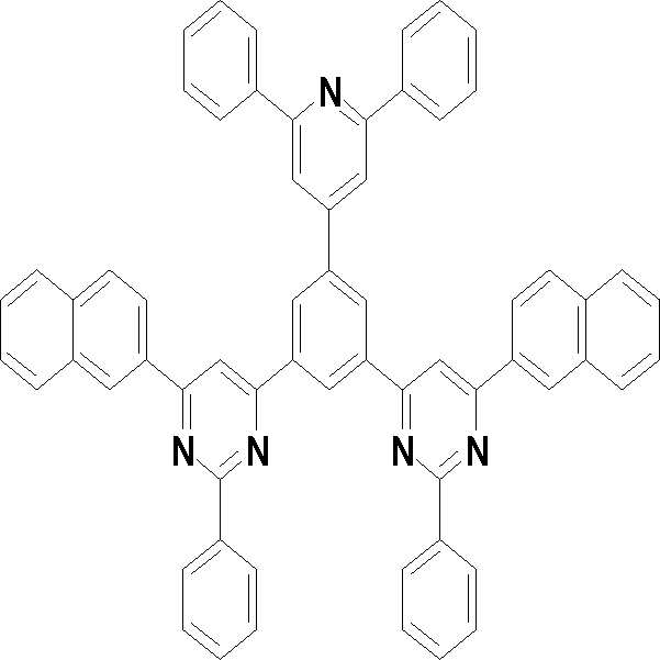
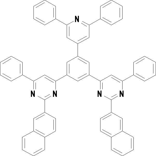
[화학식 7] [화학식 8][Formula 7] [Formula 8]


[화학식 9] [화학식 10][Formula 9] [Formula 10]

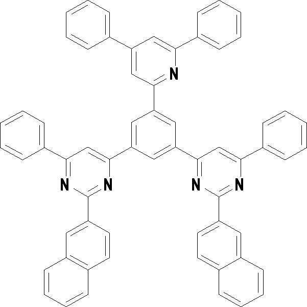
[화학식 11] [화학식 12][Formula 11] [Formula 12]

[화학식 13] [화학식 14][Formula 13] [Formula 14]

[화학식 15] [화학식 16][Formula 15] [Formula 16]


[화학식 17] [화학식 18][Formula 17] [Formula 18]
[화학식 19] [화학식 20][Formula 19] [Formula 20]

[화학식 21] [화학식 22][Formula 21] [Formula 22]


[화학식 23] [화학식 24][Formula 23] [Formula 24]
[화학식 25] [화학식 26][Formula 25] [Formula 26]

[화학식 27] [화학식 28][Formula 27] [Formula 28]

[화학식 29] [화학식 30][Formula 29] [Formula 30]


[화학식 31] [화학식 32][Formula 31] [Formula 32]

[화학식 33](33)
본 발명의 또 다른 측면에서는, 양극, 음극 및 상기 양극과 음극 사이에 개재되는 적어도 한 층 이상의 유기박막층을 포함하는 유기광전소자에 있어서, 상기 유기박막층 중 적어도 어느 한 층은 전술한 유기광전소자용 화합물을 포함하는 유기광전소자를 제공한다.In another aspect of the present invention, in the organic photoelectric device comprising an anode, a cathode and at least one organic thin film layer interposed between the anode and the cathode, at least one of the organic thin film layer for the above organic photoelectric device It provides an organic photoelectric device comprising a compound.
상기 유기박막층은 발광층, 정공수송층, 정공주입층, 전자수송층, 전자주입층, 정공차단층 및 이들의 조합을 이루어진 군에서 선택될 수 있다.The organic thin film layer may be selected from the group consisting of a light emitting layer, a hole transport layer, a hole injection layer, an electron transport layer, an electron injection layer, a hole blocking layer and a combination thereof.
상기 유기광전소자용 화합물은 전자수송층 또는 전자주입층 내에 포함될 수 있다.The compound for an organic photoelectric device may be included in an electron transport layer or an electron injection layer.
상기 유기광전소자용 화합물은 발광층 내에 포함될 수 있다.The compound for an organic photoelectric device may be included in a light emitting layer.
상기 유기광전소자용 화합물은 발광층 내에 인광 또는 형광 호스트 재료로서 사용될 수 있다.The compound for an organic photoelectric device may be used as a phosphorescent or fluorescent host material in a light emitting layer.
상기 유기 광전 소자용 화합물은 발광층 내에 형광 청색 도펀트 재료로서 사용될 수 있다.The compound for an organic photoelectric device may be used as a fluorescent blue dopant material in a light emitting layer.
상기 유기광전소자는 유기 발광 소자, 유기 태양 전지, 유기 트랜지스터, 유 기 감광체 드럼 및 유기 메모리 소자로 이루어진 군에서 선택될 수 있다.The organic photoelectric device may be selected from the group consisting of an organic light emitting device, an organic solar cell, an organic transistor, an organic photosensitive drum, and an organic memory device.
본 발명의 또 다른 측면에서는, 전술한 유기광전소자를 포함하는 표시장치를 제공한다.In still another aspect of the present invention, a display device including the organic photoelectric device described above is provided.
우수한 전기화학적 및 열적 안정성으로 수명 특성이 우수하고, 낮은 구동전압에서도 높은 발광효율을 가지는 유기광전소자를 제공할 수 있다.It is possible to provide an organic photoelectric device having excellent life characteristics due to excellent electrochemical and thermal stability and high luminous efficiency even at a low driving voltage.
이하, 본 발명의 구현예를 상세히 설명하기로 한다. 다만, 이는 예시로서 제시되는 것으로, 이에 의해 본 발명이 제한되지는 않으며 본 발명은 후술할 청구범위의 범주에 의해 정의될 뿐이다.Hereinafter, embodiments of the present invention will be described in detail. However, it should be understood that the present invention is not limited thereto, and the present invention is only defined by the scope of the following claims.
본 명세서에서 "치환"이란 별도의 정의가 없는 한, C1 내지 C30 알킬기, C1 내지 C10 알킬실릴기, C3 내지 C30 시클로알킬기, C6 내지 C30 아릴기, C1 내지 C10 알콕시기, 플루오로기, 트리플루오로메틸기 등의 C1 내지 C10 트리플루오로알킬기, 또는 시아노기로 치환된 것을 의미한다.As used herein, unless otherwise defined, C1 to C30 alkyl group, C1 to C10 alkylsilyl group, C3 to C30 cycloalkyl group, C6 to C30 aryl group, C1 to C10 alkoxy group, fluoro group, trifluoro It means substituted by C1-C10 trifluoroalkyl groups, such as a romoxy group, or a cyano group.
본 명세서에서 "헤테로"란 별도의 정의가 없는 한, 하나의 고리기내에 N, O, S 및 P로 이루어진 군에서 선택되는 헤테로 원자를 1 내지 3개 함유하고, 나머지는 탄소인 것이 바람직하다.Unless otherwise defined herein, "hetero" includes one to three heteroatoms selected from the group consisting of N, O, S, and P in one ring group, and the rest is preferably carbon.
본 명세서에서 "이들의 조합"이란 별도의 정의가 없는 한, 둘 이상의 치환기가 연결기로 결합되어 있거나, 둘 이상의 치환기가 축합하여 결합되어 있는 것을 의미한다. In the present specification, the term "combination thereof" means that two or more substituents are bonded to each other via a linking group or two or more substituents are condensed and bonded.
본 명세서에서 "알킬(alkyl)"이란 별도의 정의가 없는 한, 지방족 탄화수소 그룹을 의미한다. 알킬 부위는 어떠한 알켄이나 알킨 부위를 포함하고 있지 않음을 의미하는 "포화 알킬(saturated alkyl)" 그룹일 수 있다. 알킬 부위는 적어도 하나의 알켄 또는 알킨 부위를 포함하고 있음을 의미하는 "불포화 알킬(unsaturated alkyl)" 부위일 수도 있다. "알켄(alkene)" 부위는 적어도 두 개의 탄소원자가 적어도 하나의 탄소-탄소 이중 결합으로 이루어진 그룹을 의미하며, "알킨(alkyne)" 부위는 적어도 두 개의 탄소원자가 적어도 하나의 탄소-탄소 삼중 결합으로 이루어진 그룹을 의미한다. 포화이든 불포화이든 간에 알킬 부위는 분지형, 직쇄형 또는 환형일 수 있다. As used herein, "alkyl" refers to an aliphatic hydrocarbon group unless otherwise defined. The alkyl moiety can be a "saturated alkyl" group, meaning that it does not contain any alkenes or alkyne moieties. The alkyl moiety may be an "unsaturated alkyl" moiety, meaning that it contains at least one alkene or alkyne moiety. "Alkene" moiety means a group of at least two carbon atoms consisting of at least one carbon-carbon double bond, and an "alkyne" moiety means at least two carbon atoms having at least one carbon-carbon triple bond Means a group. The alkyl moiety, whether saturated or unsaturated, may be branched, straight chain or cyclic.
알킬 그룹은 1 내지 20 개의 탄소원자를 가질 수 있다. 알킬 그룹은 1 내지 10 개의 탄소원자들을 가지는 중간 크기의 알킬일 수도 있다. 알킬 그룹은 1 내지 6 개의 탄소원자들을 가지는 저급알킬일 수도 있다.Alkyl groups may have from 1 to 20 carbon atoms. The alkyl group may be a medium sized alkyl having 1 to 10 carbon atoms. The alkyl group may be lower alkyl having 1 to 6 carbon atoms.
예를 들어, C1 내지 C4 알킬은 알킬쇄에 1 내지 4 개의 탄소원자, 즉, 알킬쇄는 메틸, 에틸, 프로필, 이소-프로필, n-부틸, 이소-부틸, sec-부틸 및 t-부틸로 이루어진 군에서 선택됨을 나타낸다.For example, C1 to C4 alkyl is in the alkyl chain one to four carbon atoms, i.e., the alkyl chain is methyl, ethyl, propyl, iso-propyl, n-butyl, iso-butyl, sec-butyl and t-butyl Selected from the group consisting of:
전형적인 알킬 그룹에는 메틸, 에틸, 프로필, 이소프로필, 부틸, 이소부틸, t-부틸, 펜틸, 헥실, 에테닐, 프로페닐, 부테닐, 시클로프로필, 시클로부틸, 시클로펜틸, 시클로헥실 등으로부터 개별적으로 그리고 독립적으로 선택된 하나 또는 그 이상의 그룹들로 치환될 수도 있는 그룹임을 의미한다.Typical alkyl groups include, but are not limited to, methyl, ethyl, propyl, isopropyl, butyl, isobutyl, t-butyl, pentyl, hexyl, ethenyl, propenyl, butenyl, cyclopropyl, cyclobutyl, cyclopentyl, cyclohexyl, And may be substituted with one or more independently selected groups.
용어 "아릴(aryl)"은 공유 파이 전자계를 가지고 있는 적어도 하나의 링을 가지고 있는 카르보시클릭아릴(예를 들어, 페닐)을 포함하는 아릴 그룹을 의미한다. 이 용어는 모노시클릭 또는 융합 링 폴리시클릭(즉, 탄소원자들의 인접한 쌍들을 나눠 가지는 링들) 그룹들을 포함한다. 또한, 이 용어는 하나의 탄소를 접점으로 가지고 있는 스피로(spiro) 화합물을 포함한다.The term "aryl" means an aryl group including carbocyclicaryl (eg, phenyl) having at least one ring having a shared pi electron system. The term includes monocyclic or fused ring polycyclic (ie rings that divide adjacent pairs of carbon atoms) groups. The term also encompasses spiro compounds having one carbon as a contact.
용어 "헤테로아릴(heteroaryl)"은 공유 파이 전자계를 가지고 있는 적어도 하나의 링을 가지고 있는 헤테로시클릭아릴(예를 들어, 피리딘)을 포함하는 아릴 그룹을 의미한다. 이 용어는 모노시클릭 또는 융합 링 폴리시클릭(즉, 탄소원자들의 인접한 쌍들을 나눠 가지는 링들) 그룹들을 포함한다. 또한, 이 용어는 하나의 탄소를 접점으로 가지고 있는 스피로(spiro) 화합물을 포함한다.The term “heteroaryl” refers to an aryl group comprising heterocyclicaryl (eg, pyridine) having at least one ring having a shared pi electron system. The term includes monocyclic or fused ring polycyclic (ie rings that divide adjacent pairs of carbon atoms) groups. The term also encompasses spiro compounds having one carbon as a contact.
본 발명의 일 구현예에 따른 유기광전소자용 화합물은 벤젠 코어구조에 헤테로아릴기가 3개 결합된 구조일 수 있다. 상기 세 개의 치환기 결합위치는 코어 벤젠의 1, 3 및 5 위치 일 수 있다. The compound for an organic photoelectric device according to the exemplary embodiment of the present invention may have a structure in which three heteroaryl groups are bonded to a benzene core structure. The three substituent bonding positions may be 1, 3 and 5 positions of the core benzene.
또한, 상기 유기광전소자용 화합물은 코어 부분과 상기 두 개의 치환기에 다양한 치환기를 도입함으로써 다양한 에너지 밴드 갭을 갖는 화합물을 합성할 수 있으므로, 전자 주입층 및 전달층뿐만 아니라 발광층에서 요구되는 조건들을 충족시킬 수 있는 화합물들이 될 수 있다. In addition, the compound for an organic photoelectric device may synthesize a compound having various energy band gaps by introducing various substituents into the core portion and the two substituents, thereby satisfying the requirements for the emission layer as well as the electron injection layer and the transfer layer. Can be compounds.
상기 화합물의 치환기에 따라 적절한 에너지 준위를 갖는 화합물을 유기광전소자에 사용함으로써, 전자전달 능력이 강화되어 효율 및 구동전압 면에서 우수한 효과를 가지고, 전기화학적 및 열적 안정성이 뛰어나 유기광전소자 구동시 수명 특성을 향상시킬 수 있다.By using a compound having an appropriate energy level in the organic photoelectric device according to the substituent of the compound, the electron transfer ability is enhanced to have an excellent effect in terms of efficiency and driving voltage, and excellent life time when driving the organic photoelectric device due to excellent electrochemical and thermal stability. Properties can be improved.
이러한 본 발명의 일 구현예에 따르면, 하기 화학식 1 또는 2로 표시되는 유기광전소자용 화합물을 제공한다.According to one embodiment of the present invention, a compound for an organic photoelectric device represented by the following Chemical Formula 1 or 2 is provided.
[화학식 1] [화학식 2][Formula 1] [Formula 2]

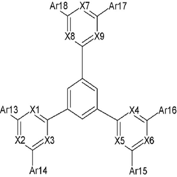
상기 화학식 1 및 2에서, X1 내지 X9는 서로 동일하거나 상이하며, 독립적으로 헤테로원자 또는 C-R이되, 상기 R은 수소, C1 내지 C30 알킬기 및 C6 내지 C30 아릴기로 이루어진 군에서 선택되고, X1 내지 X3 중 적어도 둘은 헤테로원자이며, 상기 X4 내지 X6 중 적어도 하나는 헤테로원자이며, 상기 X7 내지 X9 중 적어도 하나는 헤테로원자일 수 있다.In Chemical Formulas 1 and 2, X1 to X9 are the same as or different from each other, and independently heteroatoms or CR, wherein R is selected from the group consisting of hydrogen, C1 to C30 alkyl group, and C6 to C30 aryl group, and among X1 to X3 At least two are heteroatoms, at least one of X4 to X6 may be a heteroatom, and at least one of X7 to X9 may be a heteroatom.
상기 코어 벤젠의 치환기인 헤테로아릴기는 총 3개일 수 있으며, 이 중 하나의 헤테로아릴기는 헤테로원자가 적어도 둘 이상 포함될 수 있다. The heteroaryl group which is a substituent of the core benzene may be a total of three, and one of the heteroaryl groups may include at least two heteroatoms.
각 헤테로아릴기에 포함된 헤테로원자의 수에 따라 다양한 조합이 가능하다. 각 조합에 따라 화합물의 특성이 달라질 수 있으며, 요구되는 특성에 따라 각 조합을 선택할 수 있다.Various combinations are possible depending on the number of heteroatoms included in each heteroaryl group. The properties of the compound may vary with each combination, and each combination may be selected according to the properties required.
그 일 예로 상기 X4 내지 X6 의 헤테로원자의 수는 2일 수 있다. 그에 따라 3개의 헤테로아릴기 중에서 2개의 헤테로아릴기가 헤테로원자를 2이상 포함할 수 있게 된다.For example, the number of heteroatoms of X4 to X6 may be 2. Accordingly, two heteroaryl groups in the three heteroaryl groups may include two or more heteroatoms.
다양한 조합의 예는 다음과 같다.Examples of various combinations are as follows.
상기 X2, X3, X5, X6 및 X7이 헤테로원자인 화합물 또는 상기 X2, X3, X5, X6 및 X9가 헤테로원자인 화합물이 가능하다.Compounds in which X2, X3, X5, X6 and X7 are heteroatoms or compounds in which X2, X3, X5, X6 and X9 are heteroatoms are possible.
상기 X2, X3, X5, X6, X7 및 X9가 헤테로원자인 화합물, 상기 X2, X3, X5, X6, X8 및 X9가 헤테로원자인 화합물, 상기 X1, X3, X4, X5, X8 및 X9가 헤테로원자인 화합물, 및 상기 X1, X3, X4, X5, X7 및 X9가 헤테로원자 화합물로 이루어진 군에서 선택되는 화합물이 가능하다.The compound wherein X2, X3, X5, X6, X7 and X9 are heteroatoms, the compound X2, X3, X5, X6, X8 and X9 are heteroatoms, the X1, X3, X4, X5, X8 and X9 are heteroatoms A compound which is an atom and a compound selected from the group consisting of X1, X3, X4, X5, X7 and X9 are heteroatom compounds are possible.
상기 X2, X6, X7 및 X9가 헤테로원자인 화합물 또는 상기 X3, X5, X7 및 X9가 헤테로원자인 화합물이 가능하다.Compounds in which X2, X6, X7 and X9 are heteroatoms or compounds in which X3, X5, X7 and X9 are heteroatoms are possible.
상기 X2, X6, X7, X8 및 X9가 헤테로원자인 화합물 또는 상기 X3, X5, X7, X8 및 X9가 헤테로원자인 화합물이 가능하다.Compounds in which X2, X6, X7, X8 and X9 are heteroatoms or compounds in which X3, X5, X7, X8 and X9 are heteroatoms are possible.
상기 X2, X3, X5, X6, X7, X8 및 X9가 헤테로원자인 화합물 또는 상기 X1, X3, X4, X5, X7, X8 및 X9가 헤테로원자인 화합물이 가능하다.Compounds in which X2, X3, X5, X6, X7, X8 and X9 are heteroatoms or compounds in which X1, X3, X4, X5, X7, X8 and X9 are heteroatoms are possible.
바람직한 헤테로원자는 N 일 수 있다. 다만, 이에 제한되는 것은 아니다.Preferred heteroatoms may be N. However, it is not limited thereto.
상기 화학식 1에서, Ar1 내지 Ar6는 서로 동일하거나 상이하며, 독립적으로, 치환 또는 비치환된 C6 내지 C30 아릴렌기, 치환 또는 비치환된 C3 내지 C30 헤테로아릴렌기, 치환 또는 비치환된 C6 내지 C30 아릴아미닐렌기, 치환 또는 비치환된 카바조릴렌기, 및 치환 또는 비치환된 플루오레닐렌기로 이루어진 군에서 선택될 수 있다. In Formula 1, Ar1 to Ar6 are the same as or different from each other, and independently, a substituted or unsubstituted C6 to C30 arylene group, a substituted or unsubstituted C3 to C30 heteroarylene group, a substituted or unsubstituted C6 to C30 aryl It may be selected from the group consisting of an aminylene group, a substituted or unsubstituted carbazoylene group, and a substituted or unsubstituted fluorenylene group.
상기 Ar1 내지 Ar6의 파이공액길이(π-conjugation length)를 조절하여 가시영역에서 발광 조절을 가능하게 할 수 있다. 이로 인해, 상기 화합물이 유기광전소자의 발광층에 매우 유용하게 적용될 수 있다. 다만, 탄소수가 상기 범위를 넘게 되면 소자로서의 충분한 효과를 얻지 못할 수 있다.By controlling the pi-conjugation length of Ar1 to Ar6, light emission can be controlled in the visible region. Therefore, the compound can be very usefully applied to the light emitting layer of the organic photoelectric device. However, when the carbon number exceeds the above range, sufficient effect as the device may not be obtained.
구체적인 Ar1 내지 Ar6의 예로는 페닐렌기, 비페닐렌기, 터페닐렌기, 스틸베닐렌기, 나프틸렌기, 안트라세닐렌기, 페난트레닐렌기, 파이레닐렌기 또는 페릴레닐렌기 등이 될 수 있다.Specific examples of Ar1 to Ar6 may be a phenylene group, biphenylene group, terphenylene group, stilbenylene group, naphthylene group, anthracenylene group, phenanthrenylene group, pyrenylene group or peryleneylene group.
상기 화학식 1에서, Ar7 내지 Ar12는 서로 동일하거나 상이하며, 독립적으로 치환 또는 비치환된 C6 내지 C30 아릴기 또는 치환 또는 비치환된 C3 내지 C30 헤테로아릴기리고, a, b, c, d, e 및 f는 서로 동일하거나 상이하며, 독립적으로 1 또는 2의 정수일 수 있다.In Formula 1, Ar7 to Ar12 are the same as or different from each other, and independently a substituted or unsubstituted C6 to C30 aryl group or a substituted or unsubstituted C3 to C30 heteroaryl group, a, b, c, d, e and f is the same as or different from each other, and may independently be an integer of 1 or 2.
이러한 치환기가 결합된 구조는 열적 안정성 또는 산화에 대한 저항성이 뛰어나, 유기광전소자의 수명 특성을 향상시킬 수 있다.The structure in which the substituent is bonded is excellent in thermal stability or resistance to oxidation, thereby improving lifespan characteristics of the organic photoelectric device.
상기 치환기의 종류에 따라 화합물의 전자수송 능력을 조절할 수 있다. 또한, 화합물의 구조를 벌크하게 제조할 수 있어 결정화도를 낮출 수 있다. 화합물의 결정화도가 낮아지게 되면 소자의 수명이 길어질 수 있다.The electron transport ability of the compound can be adjusted according to the type of the substituent. In addition, the structure of the compound can be prepared in bulk, thereby lowering the crystallinity. If the crystallinity of the compound is lowered, the lifetime of the device may be longer.
Ar7 내지 Ar12의 예로는 페닐기, 비페닐기, 터페닐기, 스틸베닐기, 나프틸기, 안트라세닐기, 페난트레닐기, 파이레닐기 또는 페릴레닐기 등이 있다.Examples of Ar7 to Ar12 include a phenyl group, biphenyl group, terphenyl group, stilbenyl group, naphthyl group, anthracenyl group, phenanthrenyl group, pyrenyl group, or perrylenyl group.
또한, Ar7 내지 Ar12의 다른 예로는 티오페닐기, 퓨라닐기, 피롤일기, 이미 다졸릴기, 티아졸릴기, 옥사졸릴기, 옥사디아졸릴기, 트리아졸릴기, 피리디닐기, 피라다지닐기, 퀴놀리닐기, 이소퀴놀리닐기, 아크리디닐기, 이미다조피리디닐기, 이미다조피리미디닐기, 벤조퀴놀리닐기 또는 페난트롤리디닐기 등이 있다.Other examples of Ar7 to Ar12 include thiophenyl group, furanyl group, pyrroyl group, imidazolyl group, thiazolyl group, oxazolyl group, oxadiazolyl group, triazolyl group, pyridinyl group, pyrazinyl group, qui Nolinyl group, isoquinolinyl group, acridinyl group, imidazopyridinyl group, imidazopyrimidinyl group, benzoquinolinyl group, or phenanthrolidinyl group.
상기 화학식 2에서, Ar13 내지 Ar18는 서로 동일하거나 상이하며, 독립적으로 치환 또는 비치환된 C6 내지 C30 아릴기, 치환 또는 비치환된 C3 내지 C30 헤테로아릴기, 치환 또는 비치환된 C6 내지 C30 아릴아민기, 치환 또는 비치환된 카바조릴기 및 치환 또는 비치환된 플루오레닐기로 이루어진 군에서 선택될 수 있다. In Formula 2, Ar13 to Ar18 are the same as or different from each other, and independently a substituted or unsubstituted C6 to C30 aryl group, a substituted or unsubstituted C3 to C30 heteroaryl group, a substituted or unsubstituted C6 to C30 arylamine Groups, substituted or unsubstituted carbazoyl groups, and substituted or unsubstituted fluorenyl groups.
이러한 치환기가 결합된 구조는 열적 안정성 또는 산화에 대한 저항성이 뛰어나, 유기광전소자의 수명 특성을 향상시킬 수 있다.The structure in which the substituent is bonded is excellent in thermal stability or resistance to oxidation, thereby improving lifespan characteristics of the organic photoelectric device.
상기 치환기의 종류에 따라 화합물의 전자수송 능력을 조절할 수 있다. 또한, 화합물의 구조를 벌크하게 제조할 수 있어 결정화도를 낮출 수 있다. 화합물의 결정화도가 낮아지게 되면 소자의 수명이 길어질 수 있다.The electron transport ability of the compound can be adjusted according to the type of the substituent. In addition, the structure of the compound can be prepared in bulk, thereby lowering the crystallinity. If the crystallinity of the compound is lowered, the lifetime of the device may be longer.
Ar13 내지 Ar18의 예로는 페닐기, 비페닐기, 터페닐기, 스틸베닐기, 나프틸기, 안트라세닐기, 페난트레닐기, 파이레닐기 또는 페릴레닐기 등이 있다.Examples of Ar13 to Ar18 include a phenyl group, biphenyl group, terphenyl group, stilbenyl group, naphthyl group, anthracenyl group, phenanthrenyl group, pyrenyl group, or perrylenyl group.
또한, Ar13 내지 Ar18의 다른 예로는 티오페닐기, 퓨라닐기, 피롤일기, 이미다졸릴기, 티아졸릴기, 옥사졸릴기, 옥사디아졸릴기, 트리아졸릴기, 피리디닐기, 피라다지닐기, 퀴놀리닐기, 이소퀴놀리닐기, 아크리디닐기, 이미다조피리디닐기, 이미다조피리미디닐기, 벤조퀴놀리닐기 또는 페난트롤리디닐기 등이 있다.Other examples of Ar13 to Ar18 include thiophenyl group, furanyl group, pyrrolyl group, imidazolyl group, thiazolyl group, oxazolyl group, oxadiazolyl group, triazolyl group, pyridinyl group, pyrazazinyl group, and qui Nolinyl group, isoquinolinyl group, acridinyl group, imidazopyridinyl group, imidazopyrimidinyl group, benzoquinolinyl group, or phenanthrolidinyl group.
상기 유기광전소자용 화합물은 하기 화학식 3 내지 화학식 33으로 표시되는 것을 사용할 수 있다. 그러나 본 발명이 하기 화합물에 한정되는 것은 아니다.As the compound for an organic photoelectric device, those represented by the following Chemical Formulas 3 to 33 may be used. However, the present invention is not limited to the following compounds.
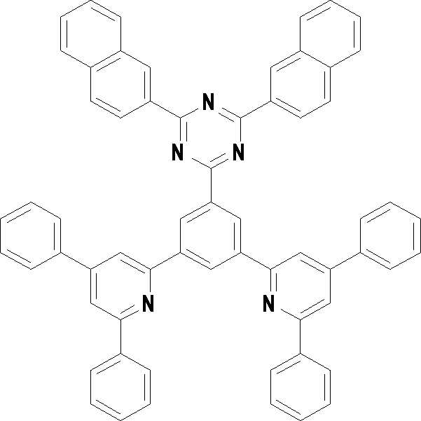
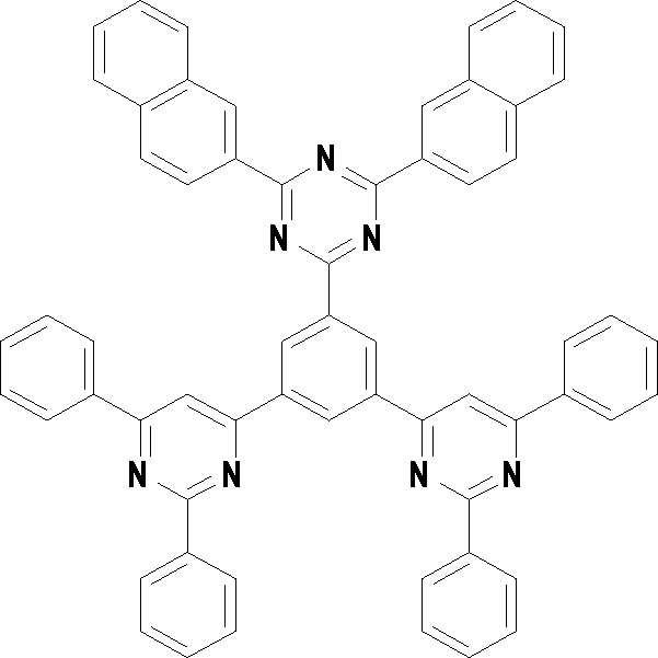
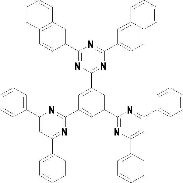
[화학식 3] [화학식 4][Formula 3] [Formula 4]
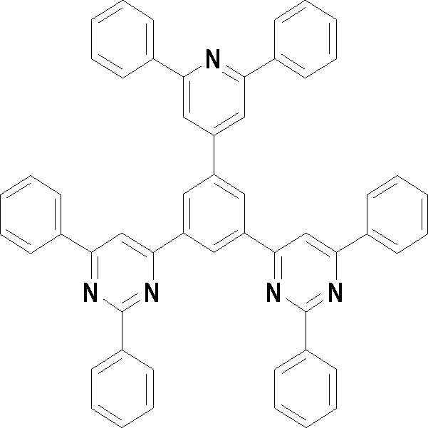

[화학식 5] [화학식 6][Formula 5] [Formula 6]


[화학식 7] [화학식 8][Formula 7] [Formula 8]
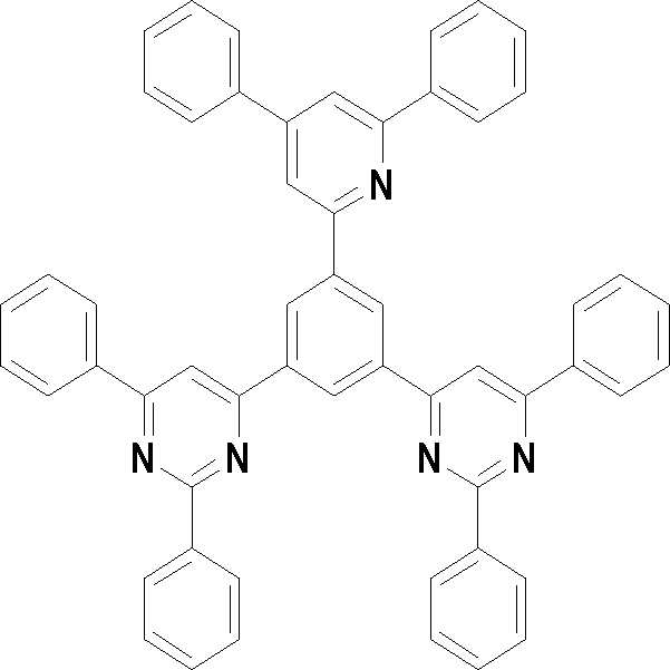

[화학식 9] [화학식 10][Formula 9] [Formula 10]
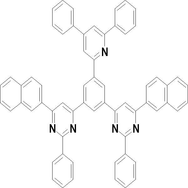

[화학식 11] [화학식 12][Formula 11] [Formula 12]


[화학식 13] [화학식 14][Formula 13] [Formula 14]


[화학식 15] [화학식 16][Formula 15] [Formula 16]


[화학식 17] [화학식 18][Formula 17] [Formula 18]


[화학식 19] [화학식 20][Formula 19] [Formula 20]

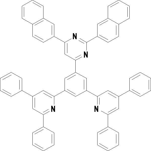
[화학식 21] [화학식 22][Formula 21] [Formula 22]


[화학식 23] [화학식 24][Formula 23] [Formula 24]


[화학식 25] [화학식 26][Formula 25] [Formula 26]


[화학식 27] [화학식 28][Formula 27] [Formula 28]


[화학식 29] [화학식 30][Formula 29] [Formula 30]
[화학식 31] [화학식 32][Formula 31] [Formula 32]

[화학식 33](33)

상기와 같은 화합물을 포함하는 유기광전소자용 화합물은 유리전이온도가 120℃ 이상이며, 열분해온도가 400℃이상으로 열적 안정성이 우수하다. 이로 인해 고효율의 유기광전소자의 구현이 가능하다. The compound for an organic photoelectric device including the compound as described above has a glass transition temperature of 120 ° C. or higher, and a thermal decomposition temperature of 400 ° C. or higher, thereby providing excellent thermal stability. As a result, it is possible to realize a highly efficient organic photoelectric device.
상기와 같은 화합물을 포함하는 유기광전소자용 화합물은 발광, 또는 전자 주입 및/또는 수송역할을 할 수 있으며, 적절한 도판트와 함께 발광 호스트로서의 역할도 할 수 있다. 즉, 상기 유기광전소자용 화합물은 인광 또는 형광의 호스트 재료, 청색의 발광도펀트 재료, 또는 전자수송 재료로 사용될 수 있다.The compound for an organic photoelectric device including the compound as described above may serve as light emission, electron injection and / or transport, and may also serve as a light emitting host with an appropriate dopant. That is, the compound for an organic photoelectric device may be used as a host material of phosphorescence or fluorescence, a blue dopant material, or an electron transport material.
본 발명의 일 구현예에 따른 유기광전소자용 화합물은 유기박막층에 사용되어 유기광전소자의 수명 특성, 효율 특성, 전기화학적 안정성 및 열적 안정성을 향 상시키며, 구동전압을 낮출 수 있다.Compound for an organic photoelectric device according to an embodiment of the present invention is used in the organic thin film layer to improve the life characteristics, efficiency characteristics, electrochemical stability and thermal stability of the organic photoelectric device, it is possible to lower the driving voltage.
이에 따라 본 발명의 일 구현예는 상기 유기광전소자용 화합물을 포함하는 유기광전소자를 제공한다. 이 때, 상기 유기광전소자라 함은 유기광전소자, 유기 태양 전지, 유기 트랜지스터, 유기 감광체 드럼, 유기 메모리 소자 등을 의미한다. 특히, 유기 태양 전지의 경우에는 본 발명의 일 구현예에 따른 유기광전소자용 화합물이 전극이나 전극 버퍼층에 포함되어 양자 효율을 증가시키며, 유기 트랜지스터의 경우에는 게이트, 소스-드레인 전극 등에서 전극 물질로 사용될 수 있다.Accordingly, one embodiment of the present invention provides an organic photoelectric device comprising the compound for an organic photoelectric device. In this case, the organic photoelectric device means an organic photoelectric device, an organic solar cell, an organic transistor, an organic photosensitive drum, an organic memory device, or the like. In particular, in the case of an organic solar cell, a compound for an organic photoelectric device according to an exemplary embodiment of the present invention is included in an electrode or an electrode buffer layer to increase quantum efficiency. Can be used.
이하에서는 유기광전소자에 대하여 구체적으로 설명한다.Hereinafter, an organic photoelectric device will be described in detail.
본 발명의 다른 일 구현예는 양극, 음극 및 상기 양극과 음극 사이에 개재되는 적어도 한 층 이상의 유기박막층을 포함하는 유기광전소자에 있어서, 상기 유기박막층 중 적어도 어느 한 층은 본 발명의 일 구현예에 따른 유기광전소자용 화합물을 포함하는 유기광전소자를 제공한다.Another embodiment of the present invention is an organic photoelectric device including a cathode, a cathode, and at least one organic thin film layer interposed between the anode and the cathode, wherein at least one of the organic thin film layers is a layer And an organic photoelectric device according to the present invention.
상기 유기광전소자용 화합물을 포함할 수 있는 유기박막층으로는 발광층, 정공수송층, 정공주입층, 전자수송층, 전자주입층, 정공차단층 및 이들의 조합으로 이루어진 군에서 선택되는 층을 포함할 수 있는 바, 이 중에서 적어도 어느 하나의 층은 본 발명에 따른 유기광전소자용 화합물을 포함한다. 특히, 전자수송층 또는 전자주입층에 본 발명의 일 구현예에 따른 유기광전소자용 화합물을 포함할 수 있다. 또한, 상기 유기광전소자용 화합물이 발광층 내에 포함되는 경우 상기 유기광전소자용 화합물은 인광 또는 형광호스트로서 포함될 수 있고, 특히, 형광 청색 도펀트 재료로서 포함될 수 있다.The organic thin film layer which may include the compound for an organic photoelectric device may include a layer selected from the group consisting of a light emitting layer, a hole transport layer, a hole injection layer, an electron transport layer, an electron injection layer, a hole blocking layer, and a combination thereof. At least one of the layers includes the compound for an organic photoelectric device according to the present invention. In particular, the electron transport layer or the electron injection layer may include a compound for an organic photoelectric device according to an embodiment of the present invention. In addition, when the compound for an organic photoelectric device is included in a light emitting layer, the compound for an organic photoelectric device may be included as a phosphorescent or fluorescent host, and in particular, may be included as a fluorescent blue dopant material.
도 1 내지 도 5는 본 발명의 일 구현예에 따른 유기광전소자용 화합물을 포함하는 유기광전소자의 단면도이다.1 to 5 are cross-sectional views of an organic photoelectric device including the compound for an organic photoelectric device according to an embodiment of the present invention.
도 1 내지 도 5를 참조하면, 본 발명의 일 구현예에 따른 유기광전소자(100, 200, 300, 400 및 500)는 양극(120), 음극(110) 및 이 양극과 음극 사이에 개재된 적어도 1층의 유기박막층(105)을 포함하는 구조를 갖는다.1 to 5, the organic
상기 양극(120)은 양극 물질을 포함하며, 이 양극 물질로는 통상 유기박막층으로 정공주입이 원활할 수 있도록 일함수가 큰 물질이 바람직하다. 상기 양극 물질의 구체적인 예로는 니켈, 백금, 바나듐, 크롬, 구리, 아연, 금과 같은 금속 또는 이들의 합금을 들 수 있고, 아연산화물, 인듐산화물, 인듐주석산화물(ITO), 인듐아연산화물(IZO)과 같은 금속 산화물을 들 수 있고, ZnO와 Al 또는 SnO2와 Sb와 같은 금속과 산화물의 조합을 들 수 있고, 폴리(3-메틸티오펜), 폴리[3,4-(에틸렌-1,2-디옥시)티오펜](polyehtylenedioxythiophene: PEDT), 폴리피롤 및 폴리아닐린과 같은 전도성 고분자 등을 들 수 있으나, 이에 한정되는 것은 아니다. 바람직하게는 상기 양극으로 ITO(indium tin oxide)를 포함하는 투명전극을 사용할 수 있다.The
상기 음극(110)은 음극 물질을 포함하여, 이 음극 물질로는 통상 유기박막층으로 전자주입이 용이하도록 일 함수가 작은 물질인 것이 바람직하다. 음극 물질의 구체적인 예로는 마그네슘, 칼슘, 나트륨, 칼륨, 타이타늄, 인듐, 이트륨, 리튬, 가돌리늄, 알루미늄, 은, 주석, 납, 세슘, 바륨 등과 같은 금속 또는 이들의 합금을 들 수 있고, LiF/Al, LiO2/Al, LiF/Ca, LiF/Al 및 BaF2/Ca과 같은 다층 구조 물질 등을 들 수 있으나, 이에 한정되는 것은 아니다. 바람직하게는 상기 음극으로 알루미늄 등과 같은 금속전극을 사용할 수 있다.The
먼저 도 1을 참조하면, 도 1은 유기박막층(105)으로서 발광층(130)만이 존재하는 유기광전소자(100)를 나타낸 것으로, 상기 유기박막층(105)은 발광층(130)만으로 존재할 수 있다.First, referring to FIG. 1, FIG. 1 illustrates an organic
도 2를 참조하면, 도 2는 유기박막층(105)으로서 전자수송층을 포함하는 발광층(230)과 정공수송층(140)이 존재하는 2층형 유기광전소자(200)를 나타낸 것으로, 도 2에 나타난 바와 같이, 유기박막층(105)은 발광층(230) 및 정공 수송층(140)을 포함하는 2층형일 수 있다. 이 경우 발광층(130)은 전자 수송층의 기능을 하며, 정공 수송층(140)은 ITO와 같은 투명전극과의 접합성 및 정공수송성을 향상시키는 기능을 한다.Referring to FIG. 2, FIG. 2 illustrates a two-layered organic
도 3을 참조하면, 도 3은 유기박막층(105)으로서 전자수송층(150), 발광층(130) 및 정공수송층(140)이 존재하는 3층형 유기광전소자(300)로서, 상기 유기박막층(105)에서 발광층(130)은 독립된 형태로 되어 있고, 전자수송성이나 정공수송성이 우수한 막(전자수송층(150) 및 정공수송층(140))을 별도의 층으로 쌓은 형태를 나타내고 있다.Referring to FIG. 3, FIG. 3 is a three-layered organic
도 4를 참조하면, 도 4는 유기박막층(105)으로서 전자주입층(160), 발광층(130), 정공수송층(140) 및 정공주입층(170)이 존재하는 4층형 유기광전소 자(400)로서, 상기 정공주입층(170)은 양극으로 사용되는 ITO와의 접합성을 향상시킬 수 있다.Referring to FIG. 4, FIG. 4 illustrates a four-layered organic
도 5를 참조하면, 도 5는 유기박막층(105)으로서 전자주입층(160), 전자수송층(150), 발광층(130), 정공수송층(140) 및 정공주입층(170)과 같은 각기 다른 기능을 하는 5개의 층이 존재하는 5층형 유기광전소자(500)를 나타내고 있으며, 상기 유기광전소자(500)는 전자주입층(160)을 별도로 형성하여 저전압화에 효과적이다.5, the organic
상기 도 1 내지 도 5에서 상기 유기박막층(105)을 이루는 전자 수송층(150), 전자 주입층(160), 발광층(130, 230), 정공 수송층(140), 정공 주입층(170) 및 이들의 조합으로 이루어진 군에서 선택되는 어느 하나는 상기 유기광전소자용 화합물을 포함한다. 이 때 상기 유기광전소자용 화합물은 상기 전자 수송층(150) 또는 전자주입층(160)을 포함하는 전자수송층(150)에 사용될 수 있으며, 그중에서도 전자수송층에 포함될 경우 정공 차단층(도시하지 않음)을 별도로 형성할 필요가 없어 보다 단순화된 구조의 유기광전소자를 제공할 수 있어 바람직하다.1 to 5, the
또한, 상기 유기 광전 소자용 화합물이 발광층(130, 230) 내에 포함되는 경우 상기 유기 광전 소자용 화합물은 인광 또는 형광호스트로서 포함될 수 있으며, 또는 형광 청색 도펀트로서 포함될 수 있다.In addition, when the compound for an organic photoelectric device is included in the
상기에서 설명한 유기광전소자는, 기판에 양극을 형성한 후, 진공증착법(evaporation), 스퍼터링(sputtering), 플라즈마 도금 및 이온도금과 같은 건식성막법; 또는 스핀코팅(spin coating), 침지법(dipping), 유동코팅법(flow coating)과 같은 습식성막법 등으로 유기박막층을 형성한 후, 그 위에 음극을 형성 하여 제조할 수 있다.The above-described organic photoelectric device may include a dry film method such as vacuum deposition, sputtering, plasma plating, and ion plating after an anode is formed on a substrate; Alternatively, the organic thin film layer may be formed by a wet film method such as spin coating, dipping, flow coating, or the like, followed by forming a cathode thereon.
본 발명의 또 다른 일 구현예에 따르면, 상기 유기광전소자를 포함하는 표시장치를 제공한다.According to another embodiment of the present invention, a display device including the organic photoelectric device is provided.
이하에서는 본 발명의 구체적인 실시예들을 제시한다. 다만, 하기에 기재된 실시예들은 본 발명을 구체적으로 예시하거나 설명하기 위한 것에 불과하며, 이로서 본 발명이 제한되어서는 아니된다.Hereinafter, specific embodiments of the present invention will be described. However, the embodiments described below are only intended to illustrate or explain the present invention, and thus the present invention should not be limited thereto.
(( 유기광전소자용For organic photoelectric device 화합물의 제조) Preparation of compounds <
실시예Example 1: 화학식 3으로 표시되는 화합물의 합성 1: Synthesis of Compound Represented by Formula 3
본 발명의 보다 구체적인 예로서 제시된 상기 화학식 3으로 표시되는 화합물은 아래의 반응식 1과 같은 경로를 통해 합성된다.Compound represented by the formula (3) given as a specific example of the present invention is synthesized through the same path as Scheme 1 below.
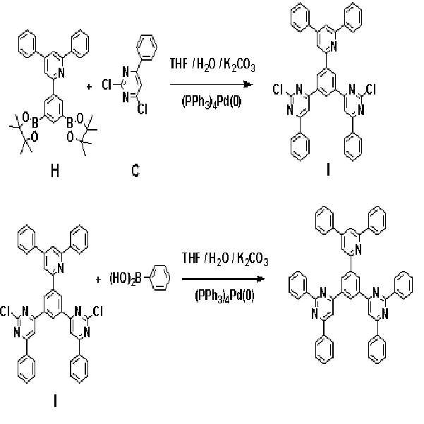
[반응식 1][Reaction Scheme 1]
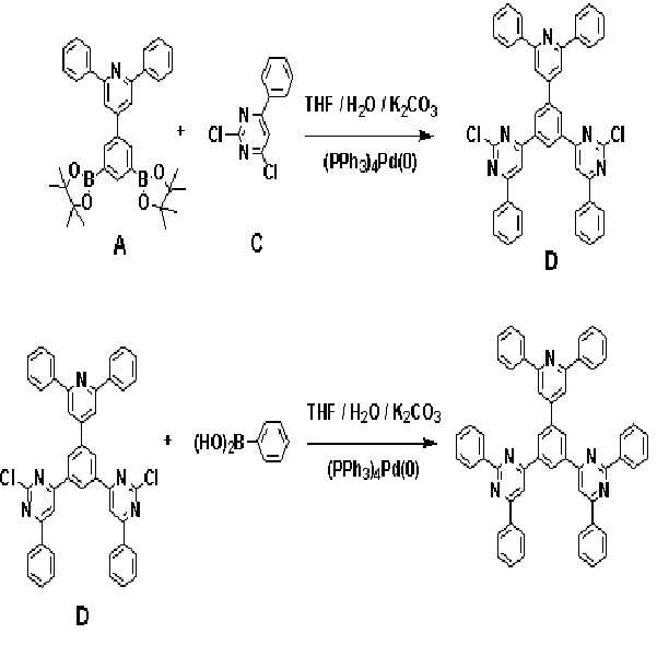
제1 단계: 중간체 생성물(D)의 합성First Step: Synthesis of Intermediate Product (D)
질소 분위기에서 온도계, 환류콘덴서, 및 교반기가 부착된 500 mL의 둥근 바닥 플라스크에 화합물 (A) 8.0 g(14.3 mmol), 화합물 (C) 8.04 g(35.7 mmol), 및 테트라키스-(트리페닐포스핀)팔라듐 0.8 g(0.69 mmol)을 300 mL 테트라하이드로퓨란과 혼합한 후, 상기 혼합용액과 2 M의 탄산칼륨(K2CO3) 100 mL을 혼합하여 70 ℃에서 12 시간 동안 교반시켰다.In a 500 mL round bottom flask equipped with a thermometer, reflux condenser, and stirrer in a nitrogen atmosphere, 8.0 g (14.3 mmol) of compound (A), 8.04 g (35.7 mmol) of compound (C), and tetrakis- (triphenylforce) Pin) palladium 0.8 g (0.69 mmol) was mixed with 300 mL tetrahydrofuran, and the mixed solution and 100 mL of 2 M potassium carbonate (K 2 CO 3 ) were mixed and stirred at 70 ° C. for 12 hours.
실온으로 냉각하여 상기 반응물의 반응을 종결한 후, 생성된 고체를 거른 다음, 메탄올로 여러 차례 씻어 준다. 최종 잔류물은 클로로포름 용매를 사용하여 실리카겔 크로마토그래피로 정제하여 중간체 생성물 (D)를 6.6 g(수율: 67.4 %) 얻었다.After cooling to room temperature to terminate the reaction, the produced solids were filtered off and washed several times with methanol. The final residue was purified by silica gel chromatography using chloroform solvent to obtain 6.6 g of an intermediate product (D) (yield: 67.4%).
제2 단계: 화학식 3으로 표시되는 화합물의 합성Second Step: Synthesis of Compound Represented by Formula 3
질소 분위기에서 온도계, 환류콘덴서, 및 교반기가 부착된 500 mL의 둥근 바닥 플라스크에 상기 제2 단계에서 합성된 중간체 생성물(D) 6.6 g(9.64 mmol), 페닐보로닉엑시드 4.42 g(24.1 mmol) 및 테트라키스-(트리페닐포스핀)팔라듐 0.7 g(0.6 mmol)을 300 mL 테트라하이드로퓨란과 혼합한 후, 상기 혼합용액과 2 M의 탄산칼륨(K2CO3) 100 mL을 혼합하여 80 ℃에서 12 시간 동안 교반시켜 흰색의 고체를 얻었다. 6.6 g (9.64 mmol) of the intermediate product (D) synthesized in the second step in a 500 mL round bottom flask equipped with a thermometer, a reflux condenser, and a stirrer in a nitrogen atmosphere, 4.42 g (24.1 mmol) phenylboronic acid And 0.7 g (0.6 mmol) of tetrakis- (triphenylphosphine) palladium with 300 mL tetrahydrofuran, followed by mixing 100 mL of 2 M potassium carbonate (K 2 CO 3 ) with 80 ° C. Was stirred for 12 hours to obtain a white solid.
실온으로 냉각하여 상기 반응물의 반응을 종결한 후, 탄산칼륨 용액을 제거하여 상기 흰색의 고체를 걸렀다. 걸러진 흰색의 고체를 테트라하이드로퓨란으로 3회 세척하고, 물로 3회 세척하고, 메탄올로 3회 세척한 후, 건조시켰다. 이 고체를 모노클로로벤젠에 녹인후 활성탄을 넣어 30분 동안 교반시키고 이 용액을 실리카켈을 통하여 필터 하였다. 필터한 모노클로로벤젠을 소량만 남기고 제거 하면 흰색의 고체가 생 되며 이 고체를 걸러 화학식 3으로 표시되는 화합물을 5.8 g(수율: 78.3 %) 얻었다.After cooling to room temperature to terminate the reaction of the reactant, the potassium carbonate solution was removed to filter the white solid. The filtered white solid was washed three times with tetrahydrofuran, three times with water, three times with methanol and then dried. The solid was dissolved in monochlorobenzene, activated carbon was added and stirred for 30 minutes, and the solution was filtered through silica gel. When the filtered monochlorobenzene was removed with only a small amount, a white solid was formed. The solid was filtered to obtain 5.8 g (yield: 78.3%) of the compound represented by Formula 3.
상기 수득된 유기광전소자용 화합물을 원소분석으로 분석한 결과는 다음과 같았다The obtained compound for an organic photoelectric device was analyzed by elemental analysis. The results were as follows.
Calcd: C, 86.02; H, 4.86; N, 9.12Calcd: C, 86.02; H, 4.86; N, 9.12
Found: C, 86.03; H, 4.85; N, 9.12Found: C, 86.03; H, 4. 85; N, 9.12
실시예Example 2: 화학식 7로 표시되는 화합물의 합성 2: Synthesis of Compound Represented by Formula 7
본 발명의 보다 구체적인 예로서 제시된 상기 화학식 7로 표시되는 화합물은 아래의 반응식 2와 같은 경로를 통해 합성된다.Compound represented by the formula (7) presented as a specific example of the present invention is synthesized through the same path as Scheme 2 below.
[반응식 2][Reaction Scheme 2]
제1 단계: 중간체 생성물(I)의 합성First Step: Synthesis of Intermediate Product (I)
질소 분위기에서 온도계, 환류콘덴서, 및 교반기가 부착된 500 mL의 둥근 바닥 플라스크에 화합물 (H) 8.0 g(14.3 mmol), 화합물 (C) 8.04 g(35.7 mmol), 및 테트라키스-(트리페닐포스핀)팔라듐 0.8 g(0.69 mmol)을 300 mL 테트라하이드로퓨란과 혼합한 후, 상기 혼합용액과 2 M의 탄산칼륨(K2CO3) 100 mL을 혼합하여 70 ℃에서 12 시간 동안 교반시켰다.In a 500 mL round bottom flask equipped with a thermometer, reflux condenser, and stirrer in a nitrogen atmosphere, 8.0 g (14.3 mmol) of compound (H), 8.04 g (35.7 mmol) of compound (C), and tetrakis- (triphenylforce) Pin) palladium 0.8 g (0.69 mmol) was mixed with 300 mL tetrahydrofuran, and the mixed solution and 100 mL of 2 M potassium carbonate (K 2 CO 3 ) were mixed and stirred at 70 ° C. for 12 hours.
실온으로 냉각하여 상기 반응물의 반응을 종결한 후, 생성된 고체를 거른 다음, 메탄올로 여러 차례 씻어 준다. 최종 잔류물은 클로로포름 용매를 사용하여 실리카겔 크로마토그래피로 정제하여 중간체 생성물 (I)를 6.1 g(수율: 62.3 %) 얻었다.After cooling to room temperature to terminate the reaction, the produced solids were filtered off and washed several times with methanol. The final residue was purified by silica gel chromatography using a chloroform solvent to give 6.1 g (yield: 62.3%) of intermediate product (I).
제2 단계: 화학식 7로 표시되는 화합물의 합성Second Step: Synthesis of Compound Represented by Formula 7
질소 분위기에서 온도계, 환류콘덴서, 및 교반기가 부착된 500 mL의 둥근 바닥 플라스크에 상기 제2 단계에서 합성된 중간체 생성물(I) 6.1 g(8.91 mmol), 페닐보로닉엑시드 4.3 g(23.4 mmol) 및 테트라키스-(트리페닐포스핀)팔라듐 0.7 g(0.6 mmol)을 300 mL 테트라하이드로퓨란과 혼합한 후, 상기 혼합용액과 2 M의 탄산칼륨(K2CO3) 100 mL을 혼합하여 80 ℃에서 12 시간 동안 교반시켜 흰색의 고체를 얻었다. 6.1 g (8.91 mmol) of the intermediate product (I) synthesized in the second step in a 500 mL round bottom flask equipped with a thermometer, a reflux condenser, and a stirrer in a nitrogen atmosphere, 4.3 g (23.4 mmol) of phenylboronic acid And 0.7 g (0.6 mmol) of tetrakis- (triphenylphosphine) palladium with 300 mL tetrahydrofuran, followed by mixing 100 mL of 2 M potassium carbonate (K 2 CO 3 ) with 80 ° C. Was stirred for 12 hours to obtain a white solid.
실온으로 냉각하여 상기 반응물의 반응을 종결한 후, 탄산칼륨 용액을 제거하여 상기 흰색의 고체를 걸렀다. 걸러진 흰색의 고체를 테트라하이드로퓨란으로 3회 세척하고, 물로 3회 세척하고, 메탄올로 3회 세척한 후, 건조시켰다. 이 고체를 모노클로로벤젠에 녹인후 활성탄을 넣어 30분 동안 교반시키고 이 용액을 실리카켈을 통하여 필터 하였다. 필터한 모노클로로벤젠을 소량만 남기고 제거 하면 흰색의 고체가 생 되며 이 고체를 걸러 화학식 7로 표시되는 화합물을 5.1 g(수율: 74.5 %) 얻었다.After cooling to room temperature to terminate the reaction of the reactant, the potassium carbonate solution was removed to filter the white solid. The filtered white solid was washed three times with tetrahydrofuran, three times with water, three times with methanol and then dried. The solid was dissolved in monochlorobenzene, activated carbon was added and stirred for 30 minutes, and the solution was filtered through silica gel. Removal of the filtered monochlorobenzene with only a small amount gave a white solid, which was filtered to obtain 5.1 g (yield: 74.5%) of a compound represented by the formula (7).
상기 수득된 유기광전소자용 화합물을 원소분석으로 분석한 결과는 다음과 같았다The obtained compound for an organic photoelectric device was analyzed by elemental analysis. The results were as follows.
Calcd: C, 86.02; H, 4.86; N, 9.12Calcd: C, 86.02; H, 4.86; N, 9.12
Found: C, 86.06; H, 4.84; N, 9.10Found: C, 86.06; H, 4.84; N, 9.10
실시예Example 3: 화학식 11로 표시되는 화합물의 합성 3: synthesis of a compound represented by formula (11)
본 발명의 보다 구체적인 예로서 제시된 상기 화학식 11로 표시되는 화합물은 아래의 반응식 3과 같은 경로를 통해 합성된다.Compound represented by the formula (11) given as a specific example of the present invention is synthesized through the same path as Scheme 3 below.
[반응식 3]Scheme 3

제1단계: 화학식 11로 표시되는 화합물의 합성First step: synthesis of the compound represented by formula (11)
질소 분위기에서 온도계, 환류콘덴서, 및 교반기가 부착된 500 mL의 둥근 바닥 플라스크에 화합물 A 6.0 g(10.72 mmol), 화합물 B 6.58g(24.67 mmol) 및 테트라키스-(트리페닐포스핀)팔라듐 0.8 g(0.69 mmol)을 300 mL 테트라하이드로퓨란과 혼합한 후, 상기 혼합용액과 2 M의 탄산칼륨(K2CO3) 100 mL을 혼합하여 80 ℃에서 12 시간 동안 교반시켜 흰색의 고체를 얻었다. 6.0 g (10.72 mmol) of Compound A, 6.58 g (24.67 mmol) of Compound B and 0.8 g of tetrakis- (triphenylphosphine) palladium in a 500 mL round bottom flask equipped with a thermometer, reflux condenser and stirrer in a nitrogen atmosphere. (0.69 mmol) was mixed with 300 mL tetrahydrofuran, and the mixed solution and 100 mL of 2 M potassium carbonate (K 2 CO 3 ) were mixed and stirred at 80 ° C. for 12 hours to obtain a white solid.
실온으로 냉각하여 상기 반응물의 반응을 종결한 후, 탄산칼륨 용액을 제거하여 상기 흰색의 고체를 걸렀다. 걸러진 흰색의 고체를 테트라하이드로퓨란으로 3회 세척하고, 물로 3회 세척하고, 메탄올로 3회 세척한 후, 건조시켰다. 이 고체를 모노클로로벤젠에 녹인후 활성탄을 넣어 30분 동안 교반시키고 이 용액을 실리카켈을 통하여 필터 하였다. 필터한 모노클로로벤젠을 소량만 남기고 제거 하면 흰색의 고체가 생 되며 이 고체를 걸러 화학식 11로 표시되는 화합물을 7.1 g(수율: 86.2 %) 얻었다.After cooling to room temperature to terminate the reaction of the reactant, the potassium carbonate solution was removed to filter the white solid. The filtered white solid was washed three times with tetrahydrofuran, three times with water, three times with methanol and then dried. The solid was dissolved in monochlorobenzene, activated carbon was added and stirred for 30 minutes, and the solution was filtered through silica gel. When the filtered monochlorobenzene was removed with only a small amount, a white solid was formed. The solid was filtered to obtain 7.1 g (yield: 86.2%) of the compound represented by Formula 11.
상기 수득된 유기광전소자용 화합물을 원소분석으로 분석한 결과는 다음과 같았다The obtained compound for an organic photoelectric device was analyzed by elemental analysis. The results were as follows.
Calcd: C, 86.02; H, 4.86; N, 9.12Calcd: C, 86.02; H, 4.86; N, 9.12
Found: C, 86.01; H, 4.87; N, 9.12Found: C, 86.01; H, 4.87; N, 9.12
실시예Example 4: 화학식 14로 표시되는 화합물의 합성 4: synthesis of compound represented by formula (14)
본 발명의 보다 구체적인 예로서 제시된 상기 화학식 14로 표시되는 화합물은 아래의 반응식 4와 같은 경로를 통해 합성된다.Compound represented by the formula (14) given as a specific example of the present invention is synthesized through the same path as Scheme 4 below.
[반응식 4][Reaction Scheme 4]

제1단계: 화학식 14로 표시되는 화합물의 합성First Step: Synthesis of Compound Represented by Formula 14
질소 분위기에서 온도계, 환류콘덴서, 및 교반기가 부착된 500 mL의 둥근 바닥 플라스크에 화합물 H 6.0 g(10.72 mmol), 화합물 B 6.58g(24.67 mmol) 및 테트라키스-(트리페닐포스핀)팔라듐 0.8 g(0.69 mmol)을 300 mL 테트라하이드로퓨란과 혼합한 후, 상기 혼합용액과 2 M의 탄산칼륨(K2CO3) 100 mL을 혼합하여 80 ℃에서 12 시간 동안 교반시켜 흰색의 고체를 얻었다. In a 500 mL round bottom flask equipped with a thermometer, reflux condenser, and stirrer in a nitrogen atmosphere, 6.0 g (10.72 mmol) of Compound H, 6.58 g (24.67 mmol) of Compound B and 0.8 g of tetrakis- (triphenylphosphine) palladium (0.69 mmol) was mixed with 300 mL tetrahydrofuran, and the mixed solution and 100 mL of 2 M potassium carbonate (K 2 CO 3 ) were mixed and stirred at 80 ° C. for 12 hours to obtain a white solid.
실온으로 냉각하여 상기 반응물의 반응을 종결한 후, 탄산칼륨 용액을 제거하여 상기 흰색의 고체를 걸렀다. 걸러진 흰색의 고체를 테트라하이드로퓨란으로 3회 세척하고, 물로 3회 세척하고, 메탄올로 3회 세척한 후, 건조시켰다. 이 고체를 모노클로로벤젠에 녹인후 활성탄을 넣어 30분 동안 교반시키고 이 용액을 실리카켈을 통하여 필터 하였다. 필터한 모노클로로벤젠을 소량만 남기고 제거 하면 흰색의 고체가 생 되며 이 고체를 걸러 화학식 14로 표시되는 화합물을 6.9 g(수율: 83.8%) 얻었다.After cooling to room temperature to terminate the reaction of the reactant, the potassium carbonate solution was removed to filter the white solid. The filtered white solid was washed three times with tetrahydrofuran, three times with water, three times with methanol and then dried. The solid was dissolved in monochlorobenzene, activated carbon was added and stirred for 30 minutes, and the solution was filtered through silica gel. When the filtered monochlorobenzene was removed with only a small amount, a white solid was formed. The solid was filtered to obtain 6.9 g (yield: 83.8%) of the compound represented by Formula 14.
상기 수득된 유기광전소자용 화합물을 원소분석으로 분석한 결과는 다음과 같았다The obtained compound for an organic photoelectric device was analyzed by elemental analysis. The results were as follows.
Calcd: C, 86.02; H, 4.86; N, 9.12Calcd: C, 86.02; H, 4.86; N, 9.12
Found: C, 86.03; H, 4.87; N, 9.10Found: C, 86.03; H, 4.87; N, 9.10
실시예 5: 화학식 19로 표시되는 화합물의 합성Example 5: Synthesis of Compound Represented by Formula 19
본 발명의 보다 구체적인 예로서 제시된 상기 화학식 19로 표시되는 화합물은 아래의 반응식 5와 같은 경로를 통해 합성된다.Compound represented by the formula (19) presented as a specific example of the present invention is synthesized through the same path as Scheme 5 below.
[반응식 5]Scheme 5

제1단계: 화학식 19로 표시되는 화합물의 합성First step: synthesis of a compound represented by formula (19)
질소 분위기에서 온도계, 환류콘덴서, 및 교반기가 부착된 500 mL의 둥근 바닥 플라스크에 화합물 E 6.0 g(10.7 mmol), 화합물 G 7.63g(24.6 mmol) 및 테트라키스-(트리페닐포스핀)팔라듐 0.8 g(0.69 mmol)을 300 mL 테트라하이드로퓨란과 혼합한 후, 상기 혼합용액과 2 M의 탄산칼륨(K2CO3) 100 mL을 혼합하여 80 ℃에서 12 시간 동안 교반시켜 흰색의 고체를 얻었다. In a 500 mL round bottom flask equipped with a thermometer, reflux condenser, and stirrer in a nitrogen atmosphere, 6.0 g (10.7 mmol) of Compound E, 7.63 g (24.6 mmol) of Compound G and 0.8 g of tetrakis- (triphenylphosphine) palladium (0.69 mmol) was mixed with 300 mL tetrahydrofuran, and the mixed solution and 100 mL of 2 M potassium carbonate (K 2 CO 3 ) were mixed and stirred at 80 ° C. for 12 hours to obtain a white solid.
실온으로 냉각하여 상기 반응물의 반응을 종결한 후, 탄산칼륨 용액을 제거하여 상기 흰색의 고체를 걸렀다. 걸러진 흰색의 고체를 테트라하이드로퓨란으로 3회 세척하고, 물로 3회 세척하고, 메탄올로 3회 세척한 후, 건조시켰다. 이 고체를 모노클로로벤젠에 녹인후 활성탄을 넣어 30분 동안 교반시키고 이 용액을 실리카켈을 통하여 필터 하였다. 필터한 모노클로로벤젠을 소량만 남기고 제거 하면 흰색의 고체가 생 되며 이 고체를 걸러 화학식 19로 표시되는 화합물을 7.3 g(수율: 88.9 %) 얻었다.After cooling to room temperature to terminate the reaction of the reactant, the potassium carbonate solution was removed to filter the white solid. The filtered white solid was washed three times with tetrahydrofuran, three times with water, three times with methanol and then dried. The solid was dissolved in monochlorobenzene, activated carbon was added and stirred for 30 minutes, and the solution was filtered through silica gel. When the filtered monochlorobenzene was removed with only a small amount, a white solid was formed. The solid was filtered to obtain 7.3 g (yield: 88.9%) of the compound represented by Formula 19.
상기 수득된 유기광전소자용 화합물을 원소분석으로 분석한 결과는 다음과 같았다The obtained compound for an organic photoelectric device was analyzed by elemental analysis. The results were as follows.
Calcd: C, 87.70; H, 4.99; N, 7.31Calcd: C, 87.70; H, 4.99; N, 7.31
Found: C, 87.72; H, 4.97; N, 7.31Found: C, 87.72; H, 4.97; N, 7.31
실시예Example 6: 화학식 21로 표시되는 화합물의 합성 6: synthesis of a compound represented by formula 21
본 발명의 보다 구체적인 예로서 제시된 상기 화학식 21로 표시되는 화합물은 아래의 반응식 6와 같은 경로를 통해 합성된다.Compound represented by the formula 21 presented as a specific example of the present invention is synthesized through the same path as Scheme 6 below.
[반응식 6][Reaction Scheme 6]
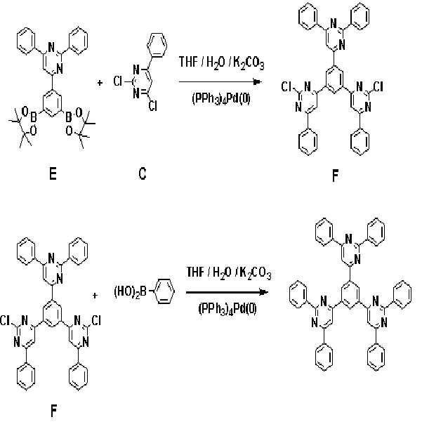
제1 단계: 중간체 생성물(F)의 합성First Step: Synthesis of Intermediate Product (F)
질소 분위기에서 온도계, 환류콘덴서, 및 교반기가 부착된 500 mL의 둥근 바닥 플라스크에 화합물 (E) 8.0 g(14.2 mmol), 화합물 (C) 8.03 g(35.6 mmol), 및 테트라키스-(트리페닐포스핀)팔라듐 0.8 g(0.69 mmol)을 300 mL 테트라하이드로퓨란과 혼합한 후, 상기 혼합용액과 2 M의 탄산칼륨(K2CO3) 100 mL을 혼합하여 70 ℃에서 12 시간 동안 교반시켰다.In a 500 mL round bottom flask equipped with a thermometer, reflux condenser, and stirrer in a nitrogen atmosphere, 8.0 g (14.2 mmol) of compound (E), 8.03 g (35.6 mmol) of compound (C), and tetrakis- (triphenylforce) Pin) palladium 0.8 g (0.69 mmol) was mixed with 300 mL tetrahydrofuran, and the mixed solution and 100 mL of 2 M potassium carbonate (K 2 CO 3 ) were mixed and stirred at 70 ° C. for 12 hours.
실온으로 냉각하여 상기 반응물의 반응을 종결한 후, 생성된 고체를 거른 다음, 메탄올로 여러 차례 씻어 준다. 최종 잔류물은 클로로포름 용매를 사용하여 실리카겔 크로마토그래피로 정제하여 중간체 생성물 (F)를 6.8 g(수율: 69.8 %) 얻었다.After cooling to room temperature to terminate the reaction, the produced solids were filtered off and washed several times with methanol. The final residue was purified by silica gel chromatography using chloroform solvent to give 6.8 g of an intermediate product (F) (yield: 69.8%).
제2 단계: 화학식 21로 표시되는 화합물의 합성Second Step: Synthesis of Compound Represented by Formula 21
질소 분위기에서 온도계, 환류콘덴서, 및 교반기가 부착된 500 mL의 둥근 바닥 플라스크에 상기 제2 단계에서 합성된 중간체 생성물(F) 6.8 g(9.91 mmol), 페닐보로닉엑시드 4.54 g(24.7 mmol) 및 테트라키스-(트리페닐포스핀)팔라듐 0.7 g(0.6 mmol)을 300 mL 테트라하이드로퓨란과 혼합한 후, 상기 혼합용액과 2 M의 탄산칼륨(K2CO3) 100 mL을 혼합하여 80 ℃에서 12 시간 동안 교반시켜 흰색의 고체를 얻었다. 6.8 g (9.91 mmol) of the intermediate product (F) synthesized in the second step in a 500 mL round bottom flask equipped with a thermometer, a reflux condenser, and a stirrer in a nitrogen atmosphere, 4.54 g (24.7 mmol) of phenylboronic acid And 0.7 g (0.6 mmol) of tetrakis- (triphenylphosphine) palladium with 300 mL tetrahydrofuran, followed by mixing 100 mL of 2 M potassium carbonate (K 2 CO 3 ) with 80 ° C. Was stirred for 12 hours to obtain a white solid.
실온으로 냉각하여 상기 반응물의 반응을 종결한 후, 탄산칼륨 용액을 제거하여 상기 흰색의 고체를 걸렀다. 걸러진 흰색의 고체를 테트라하이드로퓨란으로 3회 세척하고, 물로 3회 세척하고, 메탄올로 3회 세척한 후, 건조시켰다. 이 고체를 모노클로로벤젠에 녹인후 활성탄을 넣어 30분 동안 교반시키고 이 용액을 실리카켈을 통하여 필터 하였다. 필터한 모노클로로벤젠을 소량만 남기고 제거 하면 흰색의 고체가 생 되며 이 고체를 걸러 화학식 21로 표시되는 화합물을 5.3 g(수율: 69.5 %) 얻었다.After cooling to room temperature to terminate the reaction of the reactant, the potassium carbonate solution was removed to filter the white solid. The filtered white solid was washed three times with tetrahydrofuran, three times with water, three times with methanol and then dried. The solid was dissolved in monochlorobenzene, activated carbon was added and stirred for 30 minutes, and the solution was filtered through silica gel. Removal of the filtered monochlorobenzene with only a small amount gave a white solid, which was filtered to obtain 5.3 g (yield: 69.5%) of the compound represented by Chemical Formula 21.
상기 수득된 유기광전소자용 화합물을 원소분석으로 분석한 결과는 다음과 같았다The obtained compound for an organic photoelectric device was analyzed by elemental analysis. The results were as follows.
Calcd: C, 84.35; H, 4.72; N, 10.93Calcd: C, 84.35; H, 4.72; N, 10.93
Found: C, 84.37; H, 4.70; N, 10.93Found: C, 84.37; H, 4.70; N, 10.93
상기 합성된 재료들의 유리전이온도와 열분해온도는 DSC와 TGA로 측정하였다.The glass transition temperature and pyrolysis temperature of the synthesized materials were measured by DSC and TGA.
(( 유기광전소자의Organic photoelectric device 제조) Produce)
실시예Example 7 7
양극으로 15 Ω/cm2의 면저항값을 가진 ITO(120 nm) 유리 기판을 50 mm × 50 mm × 0.7 mm의 크기로 잘라서 이소프로필알코올과 순수물 속에서 각 5 분 동안 초음파 세정한 후, 30 분 동안 UV 오존 세정하여 사용하였다.ITO (120 nm) glass substrate with sheet resistance of 15 Ω / cm 2 was cut into 50 mm × 50 mm × 0.7 mm with an anode and ultrasonically cleaned in isopropyl alcohol and pure water for 5 minutes. Used by UV ozone rinse for minutes.
상기 기판 상부에 진공도 650×10-7 Pa, 증착속도 0.1 내지 0.3 nm/s의 조건 으로 DNTPD(40nm), N,N'-디(1-나프틸)-N,N'-디페닐벤지딘(NPB)(10nm), EB-46:EB-512 4%(40nm)을 순차적으로 열 진공 증착하여 정공주입층, 전공수송층, 발광층을 차례로 형성시켰다. DNTPD (40 nm), N, N'-di (1-naphthyl) -N, N'-diphenylbenzidine under conditions of a vacuum degree of 650 × 10 −7 Pa and a deposition rate of 0.1 to 0.3 nm / s on the substrate. NPB) (10 nm) and EB-46: EB-512 4% (40 nm) were sequentially vacuum deposited to form a hole injection layer, a hole transport layer, and a light emitting layer in that order.
이 때, 상기 도펀트의 증착속도를 조절하여, 발광층의 전체량을 100 중량%로 하였을 때, 도펀트의 배합량이 4 중량%가 되도록 증착하였다. At this time, by adjusting the deposition rate of the dopant, when the total amount of the light emitting layer to 100% by weight, the amount of the dopant was deposited so that the 4wt% by weight.
상기 발광층 상부에 동일한 열 진공 증착조건을 이용하고, 실시예 1에서 합성된 화합물 및 LiQ(1: 1 중량비)을 이용하여, 두께 30 nm의 전자수송층을 형성하였다.An electron transport layer having a thickness of 30 nm was formed using the same thermal vacuum deposition conditions on the emission layer and using the compound synthesized in Example 1 and LiQ (1: 1 weight ratio).
상기 전자수송층 상부에 동일한 열 진공 증착조건을 이용하여 음극으로서 LiQ(0.5 nm)와 Al(100 nm)을 순차적으로 증착하여 유기발광소자를 제작하였다.An organic light emitting diode was manufactured by sequentially depositing LiQ (0.5 nm) and Al (100 nm) as cathodes using the same thermal vacuum deposition conditions on the electron transport layer.
비교예Comparative example 1 One
상기 실시예 1에서 합성된 화합물 및 LiQ(1: 1 중량비)을 이용하여, 전자수송층을 형성한 것을 대신하여, 하기 화학식 34로 표시되는 화합물 및 LiQ(1: 1 중량비)을 이용한 것을 제외하고는 상기 실시예 7과 동일한 방법으로 유기발광소자를 제작하였다.Except for using the compound synthesized in Example 1 and LiQ (1: 1 weight ratio), instead of forming an electron transport layer, except that the compound represented by the formula (34) and LiQ (1: 1 weight ratio) was used. An organic light emitting device was manufactured in the same manner as in Example 7.
[화학식 34] [Formula 34]
(( 유기광전소자의Organic photoelectric device 성능 측정) Performance measurement)
실험예Experimental Example
측정 방법How to measure
이와 같이 제조된 각각의 유기광전소자에 대하여 전압에 따른 전류밀도 변화, 휘도 변화 및 발광효율을 측정하였다. 구체적인 측정방법은 다음과 같다.For each organic photoelectric device manufactured as described above, current density change, luminance change, and luminous efficiency according to voltage were measured. The specific measuring method is as follows.
1) 전압변화에 따른 전류밀도의 변화 측정1) Measurement of change of current density according to voltage change
제조된 유기광전소자에 대해, 전압을 상승시키면서 전류-전압계(Keithley 2400)를 이용하여 단위소자에 흐르는 전류값을 측정하고, 측정된 전류값을 면적으로 나누어 결과를 얻었다.With respect to the manufactured organic photoelectric device, the current value flowing through the unit device was measured using a current-voltmeter (Keithley 2400) while increasing the voltage, and the measured current value was divided by the area to obtain a result.
2) 전압변화에 따른 휘도변화 측정2) Measurement of luminance change according to voltage change
제조된 유기광전소자에 대해, 전압을 상승시키면서 휘도계(Minolta Cs-1000A)를 이용하여 그 때의 휘도를 측정하여 결과를 얻었다.The resulting organic photoelectric device was measured using a luminance meter (Minolta Cs-1000A) while increasing the voltage to obtain a result.
3) 발광효율 측정3) Luminous efficiency measurement
상기1) 및 2)로부터 측정된 휘도와 전류밀도 및 전압을 이용하여 동일 밝기(1000cd/m2)의 전류 효율(cd/A) 및 전력 효율(lm/W)을 계산하였다. 그 결과를 하기 표 1에 나타내었다.The current efficiency (cd / A) and power efficiency (lm / W) of the same brightness (1000 cd / m 2 ) were calculated using the brightness, current density, and voltage measured from 1) and 2). The results are shown in Table 1 below.
4) 색좌표는 휘도계(Minolta Cs-100A)를 이용하여 측정하였고, 그 결과를 하기 표 1에 나타내었다.4) Color coordinates were measured using a luminance meter (Minolta Cs-100A), the results are shown in Table 1 below.
측정 결과Measurement result
표 1은 상기 실시예 7 및 비교예 1에 의해 제조된 유기광전소자에 특성 평가 결과를 나타낸다. Table 1 shows the results of the characteristic evaluation on the organic photoelectric device manufactured by Example 7 and Comparative Example 1.
[표 1][Table 1]
종류device
Kinds
전압
(V)Driving
Voltage
(V)
효율
(cd/A)electric current
efficiency
(cd / A)
효율
(lm/W)power
efficiency
(lm / W)
(x, y)Color coordinates
(x, y)
상기 표 1을 참고하면, 유기발광소자의 특성 평가결과, 실시예 7에서 제조된 유기발광소자는 비교예 1의 유기발광소자와 비교하여 구동전압은 낮고, 전류효율 및 전력효율은 매우 개선된 소자 성능을 나타내는 것을 확인할 수 있었다. 상기 실시예에서 합성된 화합물은 유기발광소자의 구동전압을 낮추고, 휘도와 효율을 향상시키는 것을 확인할 수 있었다.Referring to Table 1 above, as a result of evaluating the characteristics of the organic light emitting diode, the organic light emitting diode manufactured in Example 7 has a lower driving voltage and a very improved current efficiency and power efficiency compared to the organic light emitting diode of Comparative Example 1. It was confirmed that the performance was shown. Compound synthesized in the above example was confirmed to lower the driving voltage of the organic light emitting device, improve the brightness and efficiency.
본 발명이 제시한 재료를 이용하여 제조된 유기광전소자의 특성 평가 결과, 본 발명의 일 구현예에 따른 유기광전소자는 낮은 구동전압 및 높은 발광효율을 나타내며, 따라서 소자 수명도 증가하는 것을 확인할 수 있었다.As a result of the evaluation of the characteristics of the organic photoelectric device manufactured using the material of the present invention, the organic photoelectric device according to the embodiment of the present invention shows a low driving voltage and high luminous efficiency, and thus it is confirmed that the device life is also increased. there was.
본 발명은 상기 실시예들에 한정되는 것이 아니라 서로 다른 다양한 형태로 제조될 수 있으며, 본 발명이 속하는 기술분야에서 통상의 지식을 가진 자는 본 발명의 기술적 사상이나 필수적인 특징을 변경하지 않고서 다른 구체적인 형태로 실시될 수 있다는 것을 이해할 수 있을 것이다. 그러므로 이상에서 기술한 실시예들은 모든 면에서 예시적인 것이며 한정적이 아닌 것으로 이해해야만 한다.The present invention is not limited to the above embodiments, but may be manufactured in various forms, and a person skilled in the art to which the present invention pertains has another specific form without changing the technical spirit or essential features of the present invention. It will be appreciated that the present invention may be practiced as. It is therefore to be understood that the above-described embodiments are illustrative in all aspects and not restrictive.
도 1 내지 도 5는 본 발명의 일 구현예에 따른 유기광전소자용 화합물을 이용하여 제조될 수 있는 유기광전소자에 대한 다양한 구현예들을 나타내는 단면도이다.1 to 5 are cross-sectional views illustrating various embodiments of an organic photoelectric device that may be manufactured using the compound for an organic photoelectric device according to an embodiment of the present invention.
<도면의 주요 부분에 대한 부호의 설명><Explanation of symbols for the main parts of the drawings>
100 : 유기광전소자 110 : 음극100: organic photoelectric device 110: cathode
120 : 양극 105 : 유기박막층120: anode 105: organic thin film layer
130 : 발광층 140 : 정공 수송층130: light emitting layer 140: hole transport layer
150 : 전자수송층 160 : 전자주입층150: electron transport layer 160: electron injection layer
170 : 정공주입층 230 : 발광층 + 전자수송층170: hole injection layer 230: light emitting layer + electron transport layer
Claims (18)


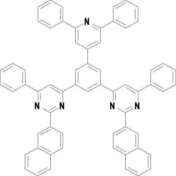

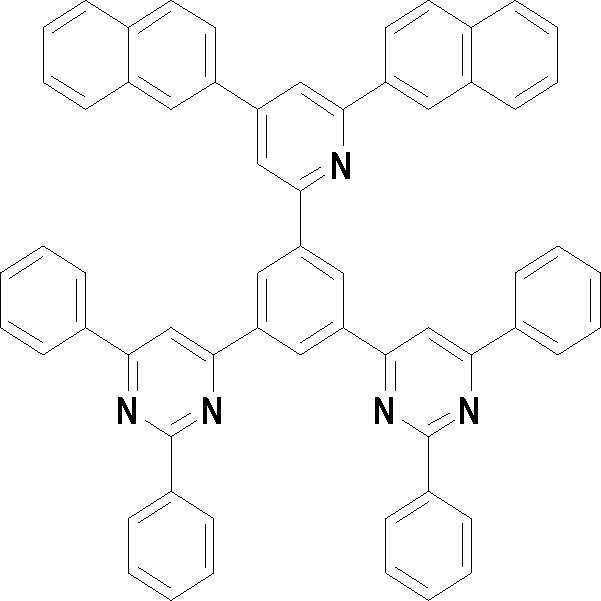


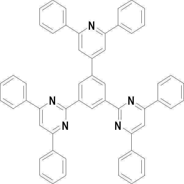
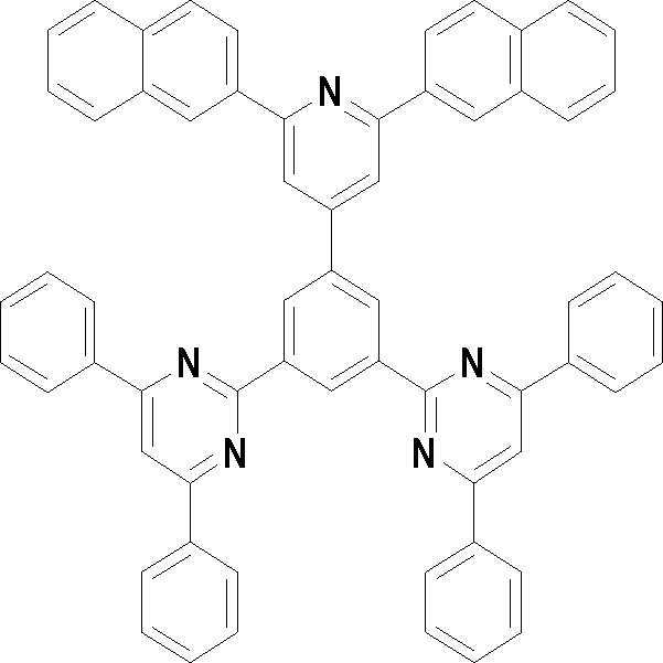


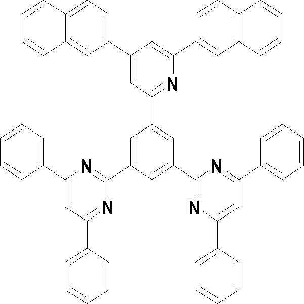


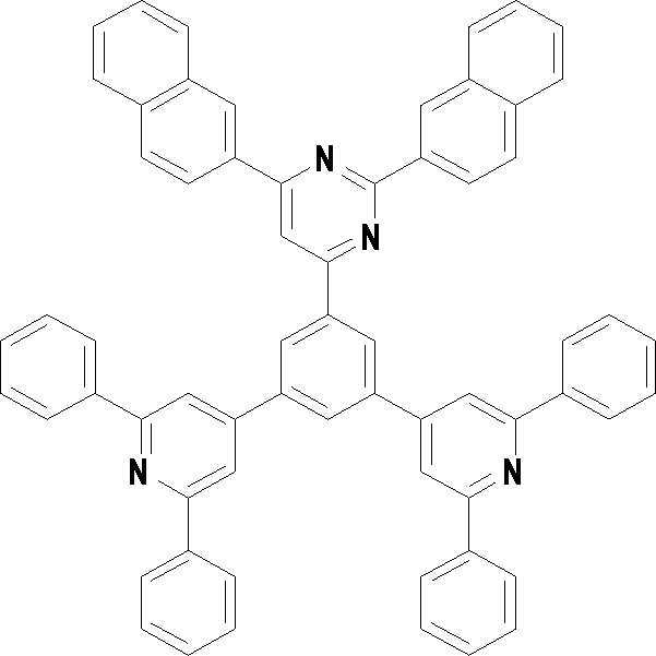


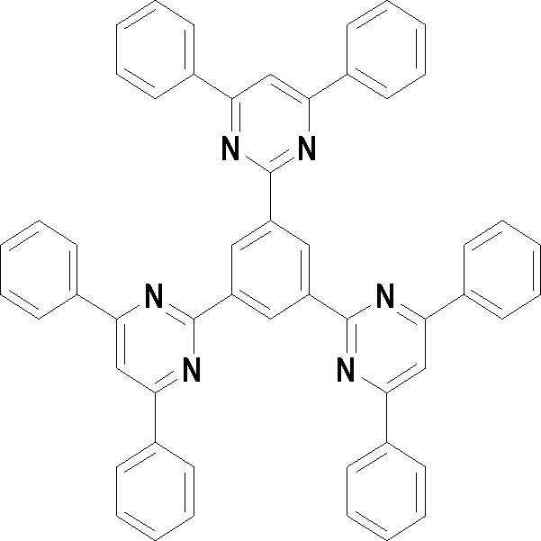

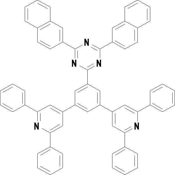

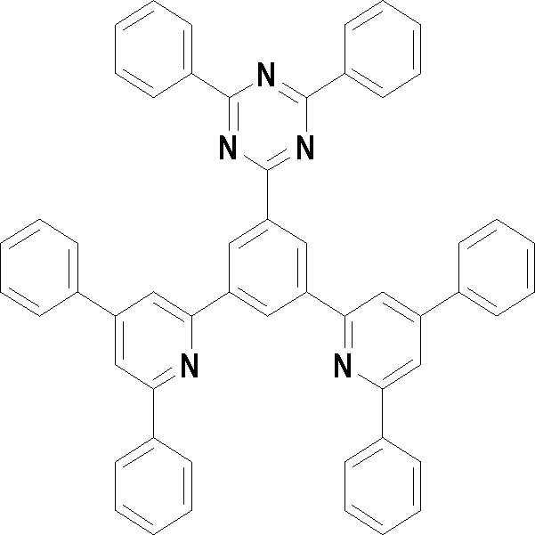


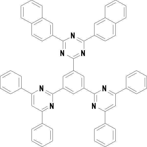
Priority Applications (6)
| Application Number | Priority Date | Filing Date | Title |
|---|---|---|---|
| KR1020090125506A KR101288566B1 (en) | 2009-12-16 | 2009-12-16 | Compound for organic photoelectric device and organic photoelectric device including the same |
| PCT/KR2010/007059 WO2011074770A2 (en) | 2009-12-16 | 2010-10-14 | Compound for organic photoelectric device and organic photoelectric device including same |
| JP2012544345A JP5782045B2 (en) | 2009-12-16 | 2010-10-14 | Compound for organic photoelectric device and organic photoelectric device including the same |
| EP10837767.2A EP2514798B1 (en) | 2009-12-16 | 2010-10-14 | Compound for organic photoelectric device and organic photoelectric device including same |
| CN201080056807.7A CN102803437B (en) | 2009-12-16 | 2010-10-14 | Compounds for organic photoelectric devices and organic photoelectric devices |
| US13/525,766 US9093652B2 (en) | 2009-12-16 | 2012-06-18 | Compound for an organic photoelectric device, organic photoelectric device including the same, and display device including the organic photoelectric device |
Applications Claiming Priority (1)
| Application Number | Priority Date | Filing Date | Title |
|---|---|---|---|
| KR1020090125506A KR101288566B1 (en) | 2009-12-16 | 2009-12-16 | Compound for organic photoelectric device and organic photoelectric device including the same |
Publications (2)
| Publication Number | Publication Date |
|---|---|
| KR20110068514A KR20110068514A (en) | 2011-06-22 |
| KR101288566B1 true KR101288566B1 (en) | 2013-07-22 |
Family
ID=44167796
Family Applications (1)
| Application Number | Title | Priority Date | Filing Date |
|---|---|---|---|
| KR1020090125506A Active KR101288566B1 (en) | 2009-12-16 | 2009-12-16 | Compound for organic photoelectric device and organic photoelectric device including the same |
Country Status (6)
| Country | Link |
|---|---|
| US (1) | US9093652B2 (en) |
| EP (1) | EP2514798B1 (en) |
| JP (1) | JP5782045B2 (en) |
| KR (1) | KR101288566B1 (en) |
| CN (1) | CN102803437B (en) |
| WO (1) | WO2011074770A2 (en) |
Cited By (1)
| Publication number | Priority date | Publication date | Assignee | Title |
|---|---|---|---|---|
| US10644245B2 (en) | 2015-06-19 | 2020-05-05 | Samsung Sdi Co., Ltd. | Composition for organic photoelectronic element, organic photoelectronic element, and display apparatus |
Families Citing this family (87)
| Publication number | Priority date | Publication date | Assignee | Title |
|---|---|---|---|---|
| US9120773B2 (en) * | 2009-08-21 | 2015-09-01 | Tosoh Corporation | Cyclic azine derivatives, processes for producing these, and organic electroluminescent element containing these as component |
| JP5660777B2 (en) * | 2009-12-21 | 2015-01-28 | 東ソー株式会社 | Cyclic azine derivative, method for producing the same, and organic electroluminescent device comprising the same |
| CN103951657A (en) * | 2014-05-09 | 2014-07-30 | 江西冠能光电材料有限公司 | High-electronegativity organic semiconductor |
| CN111205270B (en) * | 2014-06-11 | 2023-04-28 | 保土谷化学工业株式会社 | Pyrimidine Derivatives and Organic Electroluminescent Devices |
| KR102273047B1 (en) | 2014-06-30 | 2021-07-06 | 삼성디스플레이 주식회사 | Organic light-emitting device |
| KR102285388B1 (en) | 2014-11-13 | 2021-08-04 | 삼성디스플레이 주식회사 | Organic light emitting device |
| KR102456659B1 (en) * | 2014-12-26 | 2022-10-18 | 가부시키가이샤 한도오따이 에네루기 켄큐쇼 | Organic compound, light-emitting element, display module, lighting module, light-emitting device, display device, electronic device, and lighting device |
| US9929361B2 (en) | 2015-02-16 | 2018-03-27 | Universal Display Corporation | Organic electroluminescent materials and devices |
| US11056657B2 (en) | 2015-02-27 | 2021-07-06 | University Display Corporation | Organic electroluminescent materials and devices |
| US9859510B2 (en) | 2015-05-15 | 2018-01-02 | Universal Display Corporation | Organic electroluminescent materials and devices |
| US10418568B2 (en) | 2015-06-01 | 2019-09-17 | Universal Display Corporation | Organic electroluminescent materials and devices |
| KR101962758B1 (en) | 2015-06-17 | 2019-03-27 | 삼성에스디아이 주식회사 | Organic compound for optoelectric device and organic optoelectric device and display device |
| US11127905B2 (en) | 2015-07-29 | 2021-09-21 | Universal Display Corporation | Organic electroluminescent materials and devices |
| US10672996B2 (en) | 2015-09-03 | 2020-06-02 | Universal Display Corporation | Organic electroluminescent materials and devices |
| KR20170075114A (en) * | 2015-12-22 | 2017-07-03 | 삼성디스플레이 주식회사 | Organic light emitting device |
| KR102579752B1 (en) | 2015-12-22 | 2023-09-19 | 삼성디스플레이 주식회사 | Organic light emitting device |
| KR20170075122A (en) | 2015-12-22 | 2017-07-03 | 삼성디스플레이 주식회사 | Organic light emitting device |
| US20170229663A1 (en) | 2016-02-09 | 2017-08-10 | Universal Display Corporation | Organic electroluminescent materials and devices |
| US10236456B2 (en) | 2016-04-11 | 2019-03-19 | Universal Display Corporation | Organic electroluminescent materials and devices |
| US10672997B2 (en) | 2016-06-20 | 2020-06-02 | Universal Display Corporation | Organic electroluminescent materials and devices |
| US10862054B2 (en) | 2016-06-20 | 2020-12-08 | Universal Display Corporation | Organic electroluminescent materials and devices |
| US11482683B2 (en) | 2016-06-20 | 2022-10-25 | Universal Display Corporation | Organic electroluminescent materials and devices |
| US10608186B2 (en) | 2016-09-14 | 2020-03-31 | Universal Display Corporation | Organic electroluminescent materials and devices |
| US10680187B2 (en) | 2016-09-23 | 2020-06-09 | Universal Display Corporation | Organic electroluminescent materials and devices |
| US11196010B2 (en) | 2016-10-03 | 2021-12-07 | Universal Display Corporation | Organic electroluminescent materials and devices |
| US11011709B2 (en) | 2016-10-07 | 2021-05-18 | Universal Display Corporation | Organic electroluminescent materials and devices |
| US12317745B2 (en) | 2016-11-09 | 2025-05-27 | Universal Display Corporation | Organic electroluminescent materials and devices |
| US10680188B2 (en) | 2016-11-11 | 2020-06-09 | Universal Display Corporation | Organic electroluminescent materials and devices |
| US11780865B2 (en) | 2017-01-09 | 2023-10-10 | Universal Display Corporation | Organic electroluminescent materials and devices |
| US10844085B2 (en) | 2017-03-29 | 2020-11-24 | Universal Display Corporation | Organic electroluminescent materials and devices |
| US10944060B2 (en) | 2017-05-11 | 2021-03-09 | Universal Display Corporation | Organic electroluminescent materials and devices |
| US12098157B2 (en) | 2017-06-23 | 2024-09-24 | Universal Display Corporation | Organic electroluminescent materials and devices |
| US11228010B2 (en) | 2017-07-26 | 2022-01-18 | Universal Display Corporation | Organic electroluminescent materials and devices |
| US11744142B2 (en) | 2017-08-10 | 2023-08-29 | Universal Display Corporation | Organic electroluminescent materials and devices |
| US12180230B2 (en) | 2017-11-28 | 2024-12-31 | University Of Southern California | Carbene compounds and organic electroluminescent devices |
| EP3492480B1 (en) | 2017-11-29 | 2021-10-20 | Universal Display Corporation | Organic electroluminescent materials and devices |
| US11937503B2 (en) | 2017-11-30 | 2024-03-19 | Universal Display Corporation | Organic electroluminescent materials and devices |
| US11542289B2 (en) | 2018-01-26 | 2023-01-03 | Universal Display Corporation | Organic electroluminescent materials and devices |
| US11165028B2 (en) | 2018-03-12 | 2021-11-02 | Universal Display Corporation | Organic electroluminescent materials and devices |
| US12453279B2 (en) | 2018-08-22 | 2025-10-21 | Universal Display Corporation | Organic electroluminescent materials and devices |
| US11737349B2 (en) | 2018-12-12 | 2023-08-22 | Universal Display Corporation | Organic electroluminescent materials and devices |
| US11780829B2 (en) | 2019-01-30 | 2023-10-10 | The University Of Southern California | Organic electroluminescent materials and devices |
| US12477890B2 (en) | 2019-02-01 | 2025-11-18 | Universal Display Corporation | Organic electroluminescent materials and devices |
| JP2020158491A (en) | 2019-03-26 | 2020-10-01 | ユニバーサル ディスプレイ コーポレイション | Organic electroluminescent materials and devices |
| US12281128B2 (en) | 2019-07-30 | 2025-04-22 | Universal Display Corporation | Organic electroluminescent materials and devices |
| US12139501B2 (en) | 2019-08-16 | 2024-11-12 | Universal Display Corporation | Organic electroluminescent materials and devices |
| US20210135130A1 (en) | 2019-11-04 | 2021-05-06 | Universal Display Corporation | Organic electroluminescent materials and devices |
| US12538698B2 (en) | 2020-01-06 | 2026-01-27 | Universal Display Corporation | Organic electroluminescent materials and devices |
| US12426495B2 (en) | 2020-01-28 | 2025-09-23 | Universal Display Corporation | Organic electroluminescent materials and devices |
| EP3937268B1 (en) | 2020-07-10 | 2025-05-07 | Universal Display Corporation | Plasmonic oleds and vertical dipole emitters |
| US12187748B2 (en) | 2020-11-02 | 2025-01-07 | Universal Display Corporation | Organic electroluminescent materials and devices |
| US20220158096A1 (en) | 2020-11-16 | 2022-05-19 | Universal Display Corporation | Organic electroluminescent materials and devices |
| US20220165967A1 (en) | 2020-11-24 | 2022-05-26 | Universal Display Corporation | Organic electroluminescent materials and devices |
| US12325717B2 (en) | 2020-11-24 | 2025-06-10 | Universal Display Corporation | Organic electroluminescent materials and devices |
| US20220271241A1 (en) | 2021-02-03 | 2022-08-25 | Universal Display Corporation | Organic electroluminescent materials and devices |
| EP4059915B1 (en) | 2021-02-26 | 2025-12-24 | Universal Display Corporation | Organic electroluminescent materials and devices |
| EP4060758A3 (en) | 2021-02-26 | 2023-03-29 | Universal Display Corporation | Organic electroluminescent materials and devices |
| US20220298192A1 (en) | 2021-03-05 | 2022-09-22 | Universal Display Corporation | Organic electroluminescent materials and devices |
| US12428599B2 (en) | 2021-03-09 | 2025-09-30 | Universal Display Corporation | Organic electroluminescent materials and devices |
| US20220298190A1 (en) | 2021-03-12 | 2022-09-22 | Universal Display Corporation | Organic electroluminescent materials and devices |
| US12421262B2 (en) | 2021-03-15 | 2025-09-23 | Universal Display Corporation | Organic electroluminescent materials and devices |
| US20220340607A1 (en) | 2021-04-05 | 2022-10-27 | Universal Display Corporation | Organic electroluminescent materials and devices |
| US12480042B2 (en) | 2021-04-09 | 2025-11-25 | Universal Display Corporation | Organic electroluminescent materials and devices |
| EP4075531A1 (en) | 2021-04-13 | 2022-10-19 | Universal Display Corporation | Plasmonic oleds and vertical dipole emitters |
| US20220352478A1 (en) | 2021-04-14 | 2022-11-03 | Universal Display Corporation | Organic eletroluminescent materials and devices |
| US20230006149A1 (en) | 2021-04-23 | 2023-01-05 | Universal Display Corporation | Organic electroluminescent materials and devices |
| US20220407020A1 (en) | 2021-04-23 | 2022-12-22 | Universal Display Corporation | Organic electroluminescent materials and devices |
| US20230133787A1 (en) | 2021-06-08 | 2023-05-04 | University Of Southern California | Molecular Alignment of Homoleptic Iridium Phosphors |
| CN115703759B (en) * | 2021-08-10 | 2024-06-07 | 江苏三月科技股份有限公司 | Compound containing triazine and pyrimidine groups and organic electroluminescent device containing same |
| EP4151699A1 (en) | 2021-09-17 | 2023-03-22 | Universal Display Corporation | Organic electroluminescent materials and devices |
| US12473318B2 (en) | 2021-10-08 | 2025-11-18 | Universal Display Corporation | Organic electroluminescent materials and devices |
| US12509628B2 (en) | 2021-12-16 | 2025-12-30 | Universal Display Corporation | Organic electroluminescent materials and devices |
| EP4231804A3 (en) | 2022-02-16 | 2023-09-20 | Universal Display Corporation | Organic electroluminescent materials and devices |
| US20230292592A1 (en) | 2022-03-09 | 2023-09-14 | Universal Display Corporation | Organic electroluminescent materials and devices |
| US20230337516A1 (en) | 2022-04-18 | 2023-10-19 | Universal Display Corporation | Organic electroluminescent materials and devices |
| US20230389421A1 (en) | 2022-05-24 | 2023-11-30 | Universal Display Corporation | Organic electroluminescent materials and devices |
| EP4293001A1 (en) | 2022-06-08 | 2023-12-20 | Universal Display Corporation | Organic electroluminescent materials and devices |
| US20240016051A1 (en) | 2022-06-28 | 2024-01-11 | Universal Display Corporation | Organic electroluminescent materials and devices |
| US20240107880A1 (en) | 2022-08-17 | 2024-03-28 | Universal Display Corporation | Organic electroluminescent materials and devices |
| US20240180025A1 (en) | 2022-10-27 | 2024-05-30 | Universal Display Corporation | Organic electroluminescent materials and devices |
| US20240188319A1 (en) | 2022-10-27 | 2024-06-06 | Universal Display Corporation | Organic electroluminescent materials and devices |
| US20240188316A1 (en) | 2022-10-27 | 2024-06-06 | Universal Display Corporation | Organic electroluminescent materials and devices |
| US20240196730A1 (en) | 2022-10-27 | 2024-06-13 | Universal Display Corporation | Organic electroluminescent materials and devices |
| US20240188419A1 (en) | 2022-10-27 | 2024-06-06 | Universal Display Corporation | Organic electroluminescent materials and devices |
| US20240247017A1 (en) | 2022-12-14 | 2024-07-25 | Universal Display Corporation | Organic electroluminescent materials and devices |
| US20250204238A1 (en) | 2023-12-15 | 2025-06-19 | Universal Display Corporation | Organic electroluminscent materials and devices |
| US20250204239A1 (en) | 2023-12-15 | 2025-06-19 | Universal Display Corporation | Organic electroluminescent materials and devices |
Citations (2)
| Publication number | Priority date | Publication date | Assignee | Title |
|---|---|---|---|---|
| KR20090008737A (en) * | 2007-07-18 | 2009-01-22 | 제일모직주식회사 | Compound for organic photoelectric device and organic photoelectric device using same |
| WO2009142867A1 (en) | 2008-05-22 | 2009-11-26 | General Electric Company | Compound comprising phenyl pyridine units |
Family Cites Families (18)
| Publication number | Priority date | Publication date | Assignee | Title |
|---|---|---|---|---|
| JP2002324678A (en) | 2001-04-26 | 2002-11-08 | Fuji Photo Film Co Ltd | Light emitting element |
| JP4106974B2 (en) | 2002-06-17 | 2008-06-25 | コニカミノルタホールディングス株式会社 | Organic electroluminescence element and display device |
| JP4036041B2 (en) | 2002-06-24 | 2008-01-23 | コニカミノルタホールディングス株式会社 | Organic electroluminescence element and display device |
| JP2004078016A (en) | 2002-08-21 | 2004-03-11 | Kyocera Corp | Image forming device |
| JP4590825B2 (en) | 2003-02-21 | 2010-12-01 | コニカミノルタホールディングス株式会社 | White light emitting organic electroluminescence device |
| JP4487587B2 (en) * | 2003-05-27 | 2010-06-23 | 株式会社デンソー | Organic EL device and method for manufacturing the same |
| EP2592905B1 (en) * | 2003-07-31 | 2014-11-12 | Mitsubishi Chemical Corporation | Compound, charge transporting material and organic electroluminescent element |
| TWI428053B (en) * | 2004-02-09 | 2014-02-21 | Idemitsu Kosan Co | Organic electroluminescent element |
| KR20070030759A (en) | 2004-03-08 | 2007-03-16 | 이데미쓰 고산 가부시키가이샤 | Material for organic electroluminescent device and organic electroluminescent device using same |
| CN1950479A (en) | 2004-04-29 | 2007-04-18 | 西巴特殊化学品控股有限公司 | Electroluminescent device |
| KR100669724B1 (en) * | 2004-09-02 | 2007-01-16 | 삼성에스디아이 주식회사 | Terphenyl Compound and Organic Electroluminescent Device Using the Same |
| JP4907912B2 (en) | 2005-07-08 | 2012-04-04 | ケミプロ化成株式会社 | Novel 1,3,5-triphenylbenzene derivative and organic electroluminescence device containing the same |
| WO2008129912A1 (en) * | 2007-04-12 | 2008-10-30 | Tosoh Corporation | Phenyl-substituted 1,3,5-triazine compound, process for producing the same, and organic electroluminescent device containing the same as component |
| JP2009126792A (en) | 2007-11-20 | 2009-06-11 | Sagami Chem Res Center | 5-Substituted phenyl-2-trifluoromethylpyrimidin-6 (1H) -one derivative, method for producing the same, and herbicide containing the derivative as an active ingredient |
| JP5201956B2 (en) | 2007-11-20 | 2013-06-05 | ケミプロ化成株式会社 | Novel di (pyridylphenyl) derivative, electron transport material comprising the same, and organic electroluminescence device including the same |
| JP5207760B2 (en) * | 2008-02-07 | 2013-06-12 | ケミプロ化成株式会社 | Novel pyrimidine-based or triazine-based derivative, electron transport material comprising the same, and organic electroluminescence device including the same |
| US8039125B2 (en) | 2008-05-22 | 2011-10-18 | General Electric Company | Compound comprising phenyl pyridine units |
| US8317729B2 (en) * | 2008-08-18 | 2012-11-27 | Glenveigh Medical, Llc | Cervical dilation meter |
-
2009
- 2009-12-16 KR KR1020090125506A patent/KR101288566B1/en active Active
-
2010
- 2010-10-14 WO PCT/KR2010/007059 patent/WO2011074770A2/en not_active Ceased
- 2010-10-14 EP EP10837767.2A patent/EP2514798B1/en active Active
- 2010-10-14 JP JP2012544345A patent/JP5782045B2/en active Active
- 2010-10-14 CN CN201080056807.7A patent/CN102803437B/en active Active
-
2012
- 2012-06-18 US US13/525,766 patent/US9093652B2/en active Active
Patent Citations (2)
| Publication number | Priority date | Publication date | Assignee | Title |
|---|---|---|---|---|
| KR20090008737A (en) * | 2007-07-18 | 2009-01-22 | 제일모직주식회사 | Compound for organic photoelectric device and organic photoelectric device using same |
| WO2009142867A1 (en) | 2008-05-22 | 2009-11-26 | General Electric Company | Compound comprising phenyl pyridine units |
Cited By (1)
| Publication number | Priority date | Publication date | Assignee | Title |
|---|---|---|---|---|
| US10644245B2 (en) | 2015-06-19 | 2020-05-05 | Samsung Sdi Co., Ltd. | Composition for organic photoelectronic element, organic photoelectronic element, and display apparatus |
Also Published As
| Publication number | Publication date |
|---|---|
| EP2514798A4 (en) | 2014-04-16 |
| JP5782045B2 (en) | 2015-09-24 |
| US9093652B2 (en) | 2015-07-28 |
| US20120256174A1 (en) | 2012-10-11 |
| CN102803437A (en) | 2012-11-28 |
| WO2011074770A3 (en) | 2011-11-03 |
| EP2514798A2 (en) | 2012-10-24 |
| CN102803437B (en) | 2015-06-17 |
| KR20110068514A (en) | 2011-06-22 |
| EP2514798B1 (en) | 2016-09-28 |
| WO2011074770A2 (en) | 2011-06-23 |
| JP2013514348A (en) | 2013-04-25 |
Similar Documents
| Publication | Publication Date | Title |
|---|---|---|
| KR101288566B1 (en) | Compound for organic photoelectric device and organic photoelectric device including the same | |
| KR101387738B1 (en) | Compound for organic photoelectric device and organic photoelectric device including the same | |
| KR101297158B1 (en) | Compound for organic photoelectric device and organic photoelectric device including the same | |
| KR101233380B1 (en) | Novel compound for organic photoelectric device and organic photoelectric device including the same | |
| KR101506999B1 (en) | Compound for organic photoelectric device and organic photoelectric device including the same | |
| KR101531612B1 (en) | Compound for organic photoelectric device and organic photoelectric device including the same | |
| KR101212669B1 (en) | Novel compound for organic photoelectric device and organic photoelectric device including the same | |
| KR101233377B1 (en) | Novel compound for organic photoelectricand organic photoelectric device including the same | |
| KR101288557B1 (en) | Novel compound for organic photoelectric device and organic photoelectric device including the same | |
| KR101174090B1 (en) | Material for organic photoelectric device and organic photoelectric device including the same | |
| KR101297161B1 (en) | Compoundsorganic photoelectricand organic photoelectriccontaining the same | |
| KR100904070B1 (en) | Compound for organic photoelectric device and organic photoelectric device using same | |
| CN103827257B (en) | Organic light emitting diode | |
| CN104245697B (en) | Nitrogen-containing heterocyclic compounds and organic electronic devices containing them | |
| KR101247626B1 (en) | Compounds for organic photoelectric device and organic photoelectric device containing the same | |
| KR101257695B1 (en) | Novel compound for organic photoelectric device and organic photoelectric device including the same | |
| KR101566530B1 (en) | COMPOUND FOR ORGANIC OPTOELECTRONIC DEVICE, ORGANIC LiGHT EMITTING DIODE INCLUDING THE SAME AND DISPLAY INCLUDING THE ORGANIC LiGHT EMITTING DIODE | |
| KR20110079197A (en) | Compound for organic photoelectric device and organic photoelectric device comprising same | |
| KR102196624B1 (en) | Organic light emitting device | |
| KR101627748B1 (en) | COMPOUND, ORGANIC LiGHT EMITTING DIODE INCLUDING THE SAME AND DISPLAY INCLUDING THE ORGANIC LiGHT EMITTING DIODE | |
| KR102563286B1 (en) | Compound for organic optoelectronic device, organic optoelectronic device and display device | |
| KR20140085400A (en) | Compound for organic photoelectric device and organic photoelectric device including the same |
Legal Events
| Date | Code | Title | Description |
|---|---|---|---|
| PA0109 | Patent application |
Patent event code: PA01091R01D Comment text: Patent Application Patent event date: 20091216 |
|
| PG1501 | Laying open of application | ||
| A201 | Request for examination | ||
| PA0201 | Request for examination |
Patent event code: PA02012R01D Patent event date: 20110927 Comment text: Request for Examination of Application Patent event code: PA02011R01I Patent event date: 20091216 Comment text: Patent Application |
|
| E902 | Notification of reason for refusal | ||
| PE0902 | Notice of grounds for rejection |
Comment text: Notification of reason for refusal Patent event date: 20121116 Patent event code: PE09021S01D |
|
| E701 | Decision to grant or registration of patent right | ||
| PE0701 | Decision of registration |
Patent event code: PE07011S01D Comment text: Decision to Grant Registration Patent event date: 20130626 |
|
| GRNT | Written decision to grant | ||
| PR0701 | Registration of establishment |
Comment text: Registration of Establishment Patent event date: 20130716 Patent event code: PR07011E01D |
|
| PR1002 | Payment of registration fee |
Payment date: 20130716 End annual number: 3 Start annual number: 1 |
|
| PG1601 | Publication of registration | ||
| FPAY | Annual fee payment |
Payment date: 20160617 Year of fee payment: 4 |
|
| PR1001 | Payment of annual fee |
Payment date: 20160617 Start annual number: 4 End annual number: 4 |
|
| FPAY | Annual fee payment |
Payment date: 20170621 Year of fee payment: 5 |
|
| PR1001 | Payment of annual fee |
Payment date: 20170621 Start annual number: 5 End annual number: 5 |
|
| FPAY | Annual fee payment |
Payment date: 20180628 Year of fee payment: 6 |
|
| PR1001 | Payment of annual fee |
Payment date: 20180628 Start annual number: 6 End annual number: 6 |
|
| FPAY | Annual fee payment |
Payment date: 20190626 Year of fee payment: 7 |
|
| PR1001 | Payment of annual fee |
Payment date: 20190626 Start annual number: 7 End annual number: 7 |
|
| PR1001 | Payment of annual fee |
Payment date: 20200707 Start annual number: 8 End annual number: 8 |
|
| PR1001 | Payment of annual fee |
Payment date: 20210705 Start annual number: 9 End annual number: 9 |
|
| PR1001 | Payment of annual fee |
Payment date: 20220630 Start annual number: 10 End annual number: 10 |
|
| PR1001 | Payment of annual fee |
Payment date: 20230626 Start annual number: 11 End annual number: 11 |
|
| PR1001 | Payment of annual fee |
Payment date: 20240701 Start annual number: 12 End annual number: 12 |