KR101207442B1 - Method for manufacturing thin film integrated circuit device, noncontact thin film integrated circuit device and method for manufacturing the same, and idtag and coin including the noncontact thin film integrated circuit device - Google Patents
Method for manufacturing thin film integrated circuit device, noncontact thin film integrated circuit device and method for manufacturing the same, and idtag and coin including the noncontact thin film integrated circuit device Download PDFInfo
- Publication number
- KR101207442B1 KR101207442B1 KR1020117027550A KR20117027550A KR101207442B1 KR 101207442 B1 KR101207442 B1 KR 101207442B1 KR 1020117027550 A KR1020117027550 A KR 1020117027550A KR 20117027550 A KR20117027550 A KR 20117027550A KR 101207442 B1 KR101207442 B1 KR 101207442B1
- Authority
- KR
- South Korea
- Prior art keywords
- thin film
- integrated circuit
- film integrated
- circuit device
- antenna
- Prior art date
- Legal status (The legal status is an assumption and is not a legal conclusion. Google has not performed a legal analysis and makes no representation as to the accuracy of the status listed.)
- Expired - Fee Related
Links
Images


Classifications
-
- H—ELECTRICITY
- H10—SEMICONDUCTOR DEVICES; ELECTRIC SOLID-STATE DEVICES NOT OTHERWISE PROVIDED FOR
- H10D—INORGANIC ELECTRIC SEMICONDUCTOR DEVICES
- H10D86/00—Integrated devices formed in or on insulating or conducting substrates, e.g. formed in silicon-on-insulator [SOI] substrates or on stainless steel or glass substrates
- H10D86/01—Manufacture or treatment
- H10D86/021—Manufacture or treatment of multiple TFTs
- H10D86/0214—Manufacture or treatment of multiple TFTs using temporary substrates
-
- G—PHYSICS
- G06—COMPUTING OR CALCULATING; COUNTING
- G06K—GRAPHICAL DATA READING; PRESENTATION OF DATA; RECORD CARRIERS; HANDLING RECORD CARRIERS
- G06K19/00—Record carriers for use with machines and with at least a part designed to carry digital markings
- G06K19/06—Record carriers for use with machines and with at least a part designed to carry digital markings characterised by the kind of the digital marking, e.g. shape, nature, code
- G06K19/067—Record carriers with conductive marks, printed circuits or semiconductor circuit elements, e.g. credit or identity cards also with resonating or responding marks without active components
- G06K19/07—Record carriers with conductive marks, printed circuits or semiconductor circuit elements, e.g. credit or identity cards also with resonating or responding marks without active components with integrated circuit chips
- G06K19/077—Constructional details, e.g. mounting of circuits in the carrier
- G06K19/07749—Constructional details, e.g. mounting of circuits in the carrier the record carrier being capable of non-contact communication, e.g. constructional details of the antenna of a non-contact smart card
- G06K19/07758—Constructional details, e.g. mounting of circuits in the carrier the record carrier being capable of non-contact communication, e.g. constructional details of the antenna of a non-contact smart card arrangements for adhering the record carrier to further objects or living beings, functioning as an identification tag
- G06K19/0776—Constructional details, e.g. mounting of circuits in the carrier the record carrier being capable of non-contact communication, e.g. constructional details of the antenna of a non-contact smart card arrangements for adhering the record carrier to further objects or living beings, functioning as an identification tag the adhering arrangement being a layer of adhesive, so that the record carrier can function as a sticker
-
- H—ELECTRICITY
- H10—SEMICONDUCTOR DEVICES; ELECTRIC SOLID-STATE DEVICES NOT OTHERWISE PROVIDED FOR
- H10D—INORGANIC ELECTRIC SEMICONDUCTOR DEVICES
- H10D30/00—Field-effect transistors [FET]
- H10D30/01—Manufacture or treatment
- H10D30/021—Manufacture or treatment of FETs having insulated gates [IGFET]
- H10D30/031—Manufacture or treatment of FETs having insulated gates [IGFET] of thin-film transistors [TFT]
- H10D30/0312—Manufacture or treatment of FETs having insulated gates [IGFET] of thin-film transistors [TFT] characterised by the gate electrodes
- H10D30/0314—Manufacture or treatment of FETs having insulated gates [IGFET] of thin-film transistors [TFT] characterised by the gate electrodes of lateral top-gate TFTs comprising only a single gate
-
- H—ELECTRICITY
- H10—SEMICONDUCTOR DEVICES; ELECTRIC SOLID-STATE DEVICES NOT OTHERWISE PROVIDED FOR
- H10D—INORGANIC ELECTRIC SEMICONDUCTOR DEVICES
- H10D30/00—Field-effect transistors [FET]
- H10D30/01—Manufacture or treatment
- H10D30/021—Manufacture or treatment of FETs having insulated gates [IGFET]
- H10D30/031—Manufacture or treatment of FETs having insulated gates [IGFET] of thin-film transistors [TFT]
- H10D30/0321—Manufacture or treatment of FETs having insulated gates [IGFET] of thin-film transistors [TFT] comprising silicon, e.g. amorphous silicon or polysilicon
-
- H—ELECTRICITY
- H10—SEMICONDUCTOR DEVICES; ELECTRIC SOLID-STATE DEVICES NOT OTHERWISE PROVIDED FOR
- H10D—INORGANIC ELECTRIC SEMICONDUCTOR DEVICES
- H10D86/00—Integrated devices formed in or on insulating or conducting substrates, e.g. formed in silicon-on-insulator [SOI] substrates or on stainless steel or glass substrates
- H10D86/40—Integrated devices formed in or on insulating or conducting substrates, e.g. formed in silicon-on-insulator [SOI] substrates or on stainless steel or glass substrates characterised by multiple TFTs
- H10D86/60—Integrated devices formed in or on insulating or conducting substrates, e.g. formed in silicon-on-insulator [SOI] substrates or on stainless steel or glass substrates characterised by multiple TFTs wherein the TFTs are in active matrices
-
- H—ELECTRICITY
- H10—SEMICONDUCTOR DEVICES; ELECTRIC SOLID-STATE DEVICES NOT OTHERWISE PROVIDED FOR
- H10D—INORGANIC ELECTRIC SEMICONDUCTOR DEVICES
- H10D86/00—Integrated devices formed in or on insulating or conducting substrates, e.g. formed in silicon-on-insulator [SOI] substrates or on stainless steel or glass substrates
- H10D86/80—Integrated devices formed in or on insulating or conducting substrates, e.g. formed in silicon-on-insulator [SOI] substrates or on stainless steel or glass substrates characterised by multiple passive components, e.g. resistors, capacitors or inductors
Landscapes
- Engineering & Computer Science (AREA)
- Computer Hardware Design (AREA)
- Microelectronics & Electronic Packaging (AREA)
- Physics & Mathematics (AREA)
- General Physics & Mathematics (AREA)
- Theoretical Computer Science (AREA)
- Thin Film Transistor (AREA)
Abstract
낮은 비용으로 박막집적회로를 대량으로 생산하기 위해, 본 발명에 따르는 박막집적회로의 제조 방법은 기판 위에 박리층을 형성하는 단계와, 상기 박리층 위에 하지막을 형성하는 단계와, 상기 하지막 위에 복수의 박막집적회로를 형성하는 단계와, 복수의 박막집적회로 사이의 경계에 홈을 형성하는 단계와, 상기 홈에 할로겐화 불소를 포함하는 기체 또는 액체를 도입하여 박리층을 제거함으로써, 상기 복수의 박막집적회로를 분리하는 단계를 포함하는 것을 특징으로 한다.In order to mass produce a thin film integrated circuit at a low cost, a method of manufacturing a thin film integrated circuit according to the present invention comprises the steps of forming a release layer on a substrate, forming a base film on the release layer, and a plurality of the above base film Forming a thin film integrated circuit, forming a groove at a boundary between the plurality of thin film integrated circuits, and introducing a gas or a liquid containing fluoride halide into the groove to remove the exfoliation layer. And separating the integrated circuit.
Description
본 발명은, 메모리나 마이크로세서(중앙 연산부, CPU) 등을 가지고, 종이처럼 얇고 유연한 박막집적회로를 탑재한 박막집적회로의 제조 방법, 상기 박막집적회로 및 안테나로 이루어지고, 주로 인간, 동식물, 제품, 지폐 등을 식별하기 위한 카드, 태그, 라벨 등에 이용되는 박막집적회로 장치, 및 그 제조 방법에 관한 것이다.The present invention comprises a method for manufacturing a thin film integrated circuit having a memory, a microprocessor (central computing unit, CPU), etc., which is equipped with a thin film flexible and flexible thin film integrated circuit, the thin film integrated circuit and an antenna, and is mainly composed of humans, animals and plants, A thin film integrated circuit device used for a card, a tag, a label, etc. for identifying a product, a bill, and the like, and a manufacturing method thereof.
최근, 식품업계, 제조 업계 등의 모든 산업계에 있어서, 제품의 안전성이나 관리 체제의 강화를 요구하는 목소리가 높아지고 있고, 그에 따른 제품에 관한 정보량이 증가하고 있다. 그러나, 현재의 제품정보는, 주로 바코드의 십수 자리의 숫자에 의해 제공되는 제조국, 메이커, 제품번호 등의 정보 정도로, 정보량이 대단히 적었다. 또 바코드를 이용한 경우, 하나하나 수작업으로 진행하므로 판독하는 데에 시간을 필요로 했다. 그래서, 바코드 시스템을 대신하여, RFID(Radio Frequency Identification)라 불리는, 전자파를 이용한 비접촉 IC태그에 의한 자동인식 기술이 주목받고 있다.In recent years, in all industries, such as the food industry and the manufacturing industry, voices are demanded for strengthening the safety of products and management systems, and the amount of information on products is increasing. However, the current product information has a very small amount of information, such as information of a manufacturing country, a manufacturer, a product number, and the like, which are mainly provided by a ten-digit number of a barcode. In the case of using a barcode, it takes time to read because it is performed by hand one by one. Thus, in place of the barcode system, an automatic recognition technology using a non-contact IC tag using electromagnetic waves, called RFID (Radio Frequency Identification), has attracted attention.
또한 동식물의 안전성(예를 들면 원산지, 전염병의 감염의 유무 등)을 확보하기 위해서, 동식물의 체내에 직접 IC칩을 매립하고, 체외의 정보 판독 장치(reader)에 의해 동식물에 관한 정보를 취득, 관리한다는 체제가 보급되고 있다.In order to ensure the safety of plants and animals (e.g., origin, presence of infectious diseases, etc.), IC chips are embedded directly in plants and animals, and information about plants and animals is acquired by an information reader outside the body. The system of management is spreading.
또한 최근, 일인당 휴대하는 카드 수가 증가하고 있고, 그중에서도 전자계를 이용해서 통신하는 비접촉형 IC카드가, 전자 승차권이나 전자 머니 등의 형태로 보급되고 있다. 또한 흉악범죄나 행방불명 등의 사건이 증가함에 따라, 특히 유아, 아동, 노인이나 여행자 등의 개개인의 거처를 항상 적확하게 파악하여, 사고에 휩싸이는 것으로부터 보호하도록, 개개인을 인식할 수 있는 ID(Identification) 카드 등이 보급되고 있다.In recent years, the number of cards to be carried per person has increased, and among them, non-contact type IC cards communicating using an electronic system have been spread in the form of electronic tickets and electronic money. In addition, as incidents of violent crimes and disappearances increase, the identification of individual IDs (eg, infants, children, the elderly, travelers, etc.) to identify and protect individuals from being caught in an accident is always accurate. Identification cards and the like are becoming popular.
또한 지폐, 동전, 유가 증권, 티켓 등이 위조되거나 도난당했을 때에, 복제나 악용을 방지하기 위해서, 그것들의 내부에 IC칩을 매립해 두는 기술이 보급되고 있다(비특허문헌 1: 닛케이 일렉트로닉스(닛케이 BP사) 2002년 11월 18일 발행, 67-76쪽).In addition, when banknotes, coins, securities, tickets, etc. are forged or stolen, technologies for embedding IC chips inside them are popular to prevent duplication or abuse (Non-Patent Document 1: Nikkei Electronics (Nikkei Electronics) BP) issued November 18, 2002, pp. 67-76).
비접촉형이나 접촉형 IC칩이 보급됨에 따라서, 막대한 수의 인간, 동식물, 제품, 지폐 등에 이용 가능한 IC칩을, 대량으로 매우 낮은 비용으로 제조할 필요가 있다. 예를 들면 제품이나 지폐 등에 첨부되는 IC칩은, 1개당 1엔 ~ 수엔, 바람직하게는 1엔 이하의 비용으로 제조할 필요가 있고, 저비용으로 대량 생산이 가능한 IC칩의 구조, 프로세스의 실현이 요구되고 있다.As non-contact or contact IC chips become widespread, it is necessary to manufacture IC chips that can be used for a huge number of human beings, animals, plants, products, bills and the like in large quantities at very low cost. For example, an IC chip attached to a product or a bill is required to be manufactured at a cost of 1 yen to several yen, preferably 1 yen or less per unit, and the structure and process of an IC chip capable of mass production at low cost can be realized. It is required.
IC칩을 제조하는 데 있어서, 실리콘 웨이퍼 위에 복수의 박막집적회로를 형성하고, 상기 실리콘 웨이퍼를 연마 제거(백 그라인드라고 불린다.)함으로써 박막집적회로를 분리하는 방법이 이용되고 있다. 그러나, 실리콘 웨이퍼는 고가인데도 불구하고, 그것을 모두 연마 제거하므로, 제조 비용의 증가를 회피할 수 없었다. 또한 실리콘 웨이퍼로 이루어지는 집적회로는 두꺼우므로, 제품용기 자체에 탑재할 경우, 표면에 요철이 생겨, 디자인 선택의 폭에 한계가 있었다.In manufacturing an IC chip, a method of separating a thin film integrated circuit by forming a plurality of thin film integrated circuits on a silicon wafer and polishing and removing the silicon wafer (called back grind) is used. However, although silicon wafers are expensive, they are all polished and removed, and an increase in manufacturing cost could not be avoided. In addition, since an integrated circuit made of a silicon wafer is thick, when mounted in the product container itself, irregularities are formed on the surface thereof, thereby limiting the range of design choices.
또한 기판을 연마 제거하지 않는 방법으로서, 복수의 박막집적회로 등이 형성된 기판에 스트레스를 가하여, 기판을 물리적으로 박리하는 방법이 있다. 하지만, 이 방법으로는, 기판 위에 형성된 박막의 응력의 분포 등에 의해, 기판이 완전히 박리되지 않을 가능성이 있었다.As a method of not polishing and removing a substrate, there is a method of applying a stress to a substrate on which a plurality of thin film integrated circuits and the like are formed to physically peel the substrate. However, in this method, the substrate may not be completely peeled off due to the distribution of the stress of the thin film formed on the substrate.
본 발명은, 이러한 상황을 감안해서 이뤄진 것으로, 저비용으로 대량생산이 가능하며, 종래의 실리콘 웨이퍼와 달리, 대단히 막 두께가 얇은 박막집적회로, 및 상기 박막집적회로를 사용한 박막집적회로 장치 또는 IC칩의 구조, 프로세스를 제공하는 것을 목적으로 하고 있다.SUMMARY OF THE INVENTION The present invention has been made in view of such a situation, and can be mass-produced at low cost, and unlike a conventional silicon wafer, a thin film integrated circuit having a very thin film, and a thin film integrated circuit device or IC chip using the thin film integrated circuit Its purpose is to provide a structure and process.
1) 본 발명에 따른 박막집적회로의 제조 방법은, 기판 위에 박리층을 형성하고, 상기 박리층 위에 하지막을 사이에 두고 복수의 박막집적회로를 형성하고, 상기 복수의 박막집적회로 사이의 경계에 홈을 형성하고, 상기 홈에 할로겐화 불소를 포함하는 기체 또는 액체를 도입하여, 상기 박리층을 제거함으로써, 상기 복수의 박막집적회로를 분리하는 것을 특징으로 한다.1) In the method for manufacturing a thin film integrated circuit according to the present invention, a release layer is formed on a substrate, and a plurality of thin film integrated circuits are formed on the release layer with a base film interposed therebetween, and a boundary between the plurality of thin film integrated circuits is formed. A plurality of thin film integrated circuits are formed by forming a groove, introducing a gas or a liquid containing fluoride halide into the groove, and removing the release layer.
박리층은, 기판과 박막집적회로의 사이에 설치되는 층으로, 나중에 상기 박리층을 제거함으로써, 기판과 박막집적회로를 분리할 수 있다. 박리층으로는, 아모포스 실리콘, 다결정 실리콘, 단결정 실리콘, 세미 아모포스 실리콘(SAS)(미결정 실리콘이라고도 한다) 등, 실리콘(Si, 규소)을 주성분으로 하는 층을 사용할 수 있다. ClF3(삼불화염소) 등의 할로겐화 불소는, 규소를 선택적으로에칭한다는 특성이 있으므로, 박리층으로서 실리콘(Si, 규소)을 주성분으로 하는 층을 사용함으로써, ClF3을 포함하는 기체 또는 액체에 의해 상기 박리층을 용이하게 제거할 수 있다.The release layer is a layer provided between the substrate and the thin film integrated circuit, and the substrate and the thin film integrated circuit can be separated later by removing the release layer. As the release layer, a layer containing silicon (Si, silicon) as a main component may be used, such as amorphous silicon, polycrystalline silicon, monocrystalline silicon, semi-amorphous silicon (SAS) (also called microcrystalline silicon). Halogenated fluorine, such as chlorine trifluoride (ClF 3 ), has the property of selectively etching silicon, and thus a gas or liquid containing ClF 3 by using a layer composed mainly of silicon (Si, silicon) as a release layer. By this, the release layer can be easily removed.
하지막은, 박리층과 박막집적회로 사이에 설치되며, ClF3 등의 할로겐화 불소에 의한에칭으로부터, 박막집적회로를 보호하는 역할을 한다. 여기에서, ClF3 등의 할로겐화 불소는, 규소를 선택적으로에칭한다는 특성이 있는 반면, 산화규소(SiOx), 질화규소(SiNx), 산질화규소(SiOxNy(x>y) 또는 SiNxOy(x>y))는 대부분에칭되지 않는다. 따라서, 시간의 경과와 함께 박리층은에칭되어 가지만, 산화규소, 질화규소, 산질화규소(SiOxNy(x>y) 또는 SiNxOy(x>y))로 이루어진 하지막은 대부분에칭되지 않으므로, 박막집적회로의 손상을 방지할 수 있다.The base film is provided between the release layer and the thin film integrated circuit, and serves to protect the thin film integrated circuit from etching by halogenated fluorine such as ClF 3 . Here, halogenated fluorine such as ClF 3 has the property of selectively etching silicon, while silicon oxide (SiOx), silicon nitride (SiNx), silicon oxynitride (SiOxNy (x> y) or SiNxOy (x> y) Are not etched mostly. Therefore, as time passes, the release layer is etched, but since the underlying film made of silicon oxide, silicon nitride, and silicon oxynitride (SiOxNy (x> y) or SiNxOy (x> y)) is not etched mostly, damage to the thin film integrated circuit is caused. Can be prevented.
ClF3 등의 할로겐화 불소에 의해에칭되는 재료를 박리층으로서 사용하는 한편,에칭되지 않는 재료를 하지막으로 사용한다는 조건을 따른다면, 박리층 및 하지막의 조합은, 상기 재료에 한정되지 않고, 적절히 선택할 수 있다.The combination of the peeling layer and the base film is not limited to the above materials as long as the conditions for using a material etched with a halogenated fluorine such as ClF 3 as the peeling layer and using an unetched material as the base film are not limited to the above materials, You can choose.
에칭 가스로는, 상기 ClF3 등에 질소를 혼합한 가스를 사용할 수 있다. ClF3(비점 11.75℃)는 반응 공간의 온도에 따라서는 액체인 경우도 있는데, 그때는 습식에칭을 채용할 수도 있다. ClF3는 염소를 200℃ 이상에서 불소와 반응시킴으로써, Cl2(g) + 3F2(g)→ 2ClF3(g)의 과정을 거쳐서 생성할 수 있다. 상기 박리층을 에칭하고, 상기 하지막을 에칭하지 않는 에칭이라면, ClF3나 할로겐화 불소에 한정되지 않는다.Etching gas, the ClF 3 gas or the like can be used a mixture of nitrogen. ClF 3 (boiling point: 11.75 ° C.) may be a liquid depending on the temperature of the reaction space, in which case wet etching may be employed. ClF 3 can be produced by reacting chlorine with fluorine at 200 ° C. or higher, through a process of Cl 2 (g) + 3F 2 (g) → 2ClF 3 (g). If the etching is not etched, it is not limited to ClF 3 or halogenated fluoride.
박막집적회로의 경계를 이루는 홈의 형성은, 다이싱, 스크라이빙 또는 마스크를 이용한 에칭 등에 의해 행할 수 있다. 다이싱의 경우에는, 다이싱 장치(다이서)를 사용하는 블레이드 다이싱법이 일반적이다. 블레이드는 다이아몬드 연마용 입자를 매립한 숫돌로, 그 폭은 약 30 ~ 50μm이다. 이 블레이드를 고속회전시킴으로써, 박막집적회로를 분리한다. 스크라이빙의 경우에는, 다이아몬드 스크라이빙법과 레이저 스크라이빙법 등이 있다. 또한 에칭의 경우에는, 노광, 현상 공정에 의해 마스크 패턴을 형성한 후, 드라이에칭, 습식에칭 등에 의해 소자를 분리할 수 있다. 드라이에칭에 있어서는, 대기압 플라즈마법을 이용할 수 있다.The grooves forming the boundary of the thin film integrated circuit can be formed by dicing, scribing or etching using a mask. In the case of dicing, the blade dicing method using a dicing apparatus (dicer) is common. The blade is a grindstone in which diamond abrasive grains are embedded, and the width thereof is about 30 to 50 µm. By rotating the blade at high speed, the thin film integrated circuit is separated. In the case of scribing, there are a diamond scribing method and a laser scribing method. In the case of etching, after forming a mask pattern by exposure and a development process, an element can be isolate | separated by dry etching, wet etching, etc. In dry etching, an atmospheric pressure plasma method can be used.
기판으로는, 유리기판, 석영기판, 알루미나 등 절연 물질로 형성되는 기판, 실리콘 웨이퍼 기판, 후공정의 처리 온도를 견디어낼 수 있는 내열성을 가지는 플라스틱 기판 등을 사용할 수 있다. 이 경우, 산화규소(SiOx), 질화규소(SiNx), 산화질화규소(SiOxNy)(x>y), 질화산화규소(SiNxOy)(x>y)(x, y = 1, 2 ...) 등, 기판에서 불순물 등의 확산을 방지하기 위한 하지 절연막을 형성해도 된다. 또한 스테인레스 등의 금속 또는 반도체기판 등의 표면에 산화 실리콘이나 질화 실리콘 등의 절연막을 형성한 기판 등도 사용할 수 있다.As the substrate, a substrate formed of an insulating material such as a glass substrate, a quartz substrate, or alumina, a silicon wafer substrate, or a plastic substrate having heat resistance that can withstand the processing temperature of a post process may be used. In this case, silicon oxide (SiOx), silicon nitride (SiNx), silicon oxynitride (SiOxNy) (x> y), silicon nitride oxide (SiNxOy) (x> y) (x, y = 1, 2 ...) and the like, A base insulating film may be formed to prevent diffusion of impurities and the like in the substrate. Moreover, the board | substrate etc. which formed the insulating film, such as silicon oxide or silicon nitride, on the surface of metals, such as stainless, or a semiconductor substrate, can also be used.
또한 일단 IC칩을 형성한 후에, 박리된 사용 완료 기판을 재이용해도 된다. 재이용할 경우, 상기 다이싱이나 스크라이빙 공정에 의해, 기판에 흠집이 생기지 않도록 하는 것이 바람직하다. 하지만, 흠집이 생긴 경우에는, 유기수지나 무기막을 도포법이나 액적토출법(잉크젯법 등)으로 형성하여, 평탄화할 수 있다.Moreover, after forming an IC chip, you may reuse the peeled used board | substrate. In the case of reuse, it is preferable that the substrate is not scratched by the dicing or scribing step. However, in the case of scratches, an organic resin or an inorganic film can be formed by a coating method or a liquid droplet discharging method (inkjet method or the like) to planarize it.
박막집적회로를 할로겐화 불소 등에 의한 에칭으로부터 보호하기 위해서, 박막집적회로 위에 보호막을 형성해 두는 것이 바람직하다. 특히, 할로겐화 불소가스를 가열해서 에칭을 행할 경우에는, 내열성 유기수지나, 내열성 무기막을 사용하는 것이 바람직하다. 내열성 유기수지의 대표적인 것으로서, 실리콘(Si)과 산소(O)의 결합으로 골격구조가 구성되고, 치환기에 적어도 수소를 포함하는 재료, 혹은 치환기에 불소, 알킬기, 또는 방향족 탄화수소 중 적어도 일종을 가지는 재료가 있는데, 소위 실록산계 수지 등으로도 불린다. 이후, 내열성 유기수지의 경우에는, 실록산계 수지도 포함하는 것으로 한다.In order to protect the thin film integrated circuit from etching with fluorine halide or the like, it is preferable to form a protective film on the thin film integrated circuit. In particular, when etching by heating the halogenated fluorine gas, it is preferable to use a heat resistant organic resin or a heat resistant inorganic film. Representative of heat-resistant organic resins, a skeleton structure is formed by a combination of silicon (Si) and oxygen (O), and a material containing at least hydrogen as a substituent, or a material having at least one of fluorine, an alkyl group, or an aromatic hydrocarbon as a substituent. And so-called siloxane resins. Thereafter, in the case of the heat resistant organic resin, the siloxane resin is also included.
2) 본 발명에 따른 박막집적회로의 제조 방법은, 기판 위에 박리층을 형성하고, 상기 박리층 위에 하지막을 사이에 두고 복수의 박막집적회로를 형성하고, 상기 복수의 박막집적회로 사이의 경계에 홈을 형성하고, 상기 복수의 박막집적회로의 위쪽에 지그를 형성하고, 상기 홈에 할로겐화 불소를 포함하는 기체 또는 액체를 도입하여, 상기 박리층을 제거하는 것을 특징으로 한다.2) In the method for manufacturing a thin film integrated circuit according to the present invention, a release layer is formed on a substrate, and a plurality of thin film integrated circuits are formed on the release layer with a base film therebetween, and the boundary between the plurality of thin film integrated circuits is formed. A groove is formed, a jig is formed above the plurality of thin film integrated circuits, and a gas or a liquid containing fluoride halide is introduced into the groove to remove the release layer.
지그는 박리층을 제거한 후에 박막집적회로가 따로따로 분리되지 않도록, 일시적으로 박막집적회로를 고정하기 위한 지지 기판을 가리킨다. 지그는, 복수의 박막집적회로가 수평방향 혹은 높이방향으로 집적되어서 만들어진 소자마다 형성된다. 지그의 형상으로는, 후에 할로겐화 불소를 포함하는 기체 또는 액체의 도입을 쉽게 하기 위해서, 돌기부를 설치한 빗살 형태의 구조로 하는 것이 바람직하다. 하지만, 평탄한 지그를 사용해도 된다. 지그로는, 할로겐화 불소에 의해 손상되지 않는 산화규소를 주성분으로 하는 유리 기판, 석영기판, 또는 스테인레스(SUS)기판 등을 사용할 수 있다. 할로겐화 불소에 의해 손상되지 않는 재료이면, 이것들에 한정되지 않는다. 또한 지그와 박막집적회로와의 사이에는, 임시 접착을 위한 접착제가 설치된다.The jig refers to a supporting substrate for temporarily fixing the thin film integrated circuit so that the thin film integrated circuit is not separated after the peeling layer is removed. The jig is formed for each element formed by integrating a plurality of thin film integrated circuits in a horizontal direction or a height direction. As a jig shape, in order to make it easy to introduce | transduce the gas or liquid containing a fluorine halide later, it is preferable to set it as the comb-tooth-shaped structure provided with the protrusion part. However, a flat jig may be used. As the jig, a glass substrate, a quartz substrate, a stainless steel (SUS) substrate, or the like mainly composed of silicon oxide which is not damaged by fluoride halide can be used. As long as it is a material which is not damaged by fluoride halide, it is not limited to these. In addition, an adhesive for temporary bonding is provided between the jig and the thin film integrated circuit.
접착제로는, UV 광 조사에 의해 접착력(점착력)이 저하 또는 상실되는 재료를 사용할 수 있다. 또는, 3M사 제품의 포스트잇(등록상표)이나, 무어사 제품의 NOTESTIX(등록상표) 등에 사용되는 재박리 재접착 가능성 접착제를 사용해도 된다. 물론, 지그를 간단하게 뗄 수 있는 재료이면, 이것들에 한정되지 않는다.As the adhesive, a material in which the adhesive force (adhesive force) decreases or is lost by UV light irradiation can be used. Alternatively, a re-peelable re-adhesive adhesive used in 3M Corporation's post-it (registered trademark), Moore's NOTESTIX (registered trademark), or the like may be used. Of course, if it is a material which can easily remove a jig | tool, it will not be limited to these.
그 나머지의 구성에 대해서는, 상기 1)에서 서술한 본 발명에 준한다.About the remaining structure, it is based on this invention described in said 1).
3) 본 발명에 따른 비접촉형 박막집적회로 장치의 제조 방법은, 기판 위에 박리층을 형성하고, 상기 박리층 위에 하지막을 사이에 두고 복수의 박막집적회로를 형성하고, 상기 복수의 박막집적회로 위에 내열성 유기수지를 형성하고, 상기 복수의 박막집적회로 사이의 경계에 홈을 형성하고, 상기 홈에 할로겐화 불소를 포함하는 기체 또는 액체를 도입하여, 상기 박리층을 제거함으로써, 상기 복수의 박막집적회로를 분리하고, 상기 분리된 박막집적회로의 위쪽 또는 아래쪽에 안테나를 형성하는 것을 특징으로 한다.3) In the method for manufacturing a non-contact type thin film integrated circuit device according to the present invention, a release layer is formed on a substrate, a plurality of thin film integrated circuits are formed on the release layer, and a plurality of thin film integrated circuits are disposed thereon. The plurality of thin film integrated circuits are formed by forming a heat resistant organic resin, forming a groove at a boundary between the plurality of thin film integrated circuits, introducing a gas or a liquid containing fluoride halide into the grooves, and removing the release layer. Separating and to form an antenna on the top or bottom of the separated thin film integrated circuit.
여기에서 말하는 박막집적회로 장치는, 인간, 동식물, 자타의 제품, 지폐 등을 식별하거나, 그것들에 관한 정보를 축적하는 기능 등을 가진다. 또한, 여기에서 박막집적회로 장치는 ID칩(1dentification Chip), IDF(ID Flexible)칩, IC칩 등을 포함한다. 그중에서도, 전자계를 이용하여, 박막집적회로 장치에 내장된 송수신부(안테나, 안테나 회로)를 사이에 두고, 외부의 판독/기록 장치(리더/라이터)와, 통신을 행하는 것을 비접촉형 박막집적회로 장치로 한다. 박막집적회로 장치와 리더/라이터 사이에서 통신함으로써, 박막집적회로 장치가 내장된 제품 등에 관한 정보의 인식, 갱신, 관리 등을 행할 수 있다.The thin film integrated circuit device described herein has a function of identifying humans, animals and plants, other products, bills, and the like, and accumulating information about them. In addition, the thin film integrated circuit device may include an ID chip, an IDF chip, and an IC chip. Among them, a non-contact type thin film integrated circuit device which uses an electromagnetic field to communicate with an external read / write device (reader / writer) via a transceiver (antenna, antenna circuit) built in the thin film integrated circuit device. Shall be. By communicating between the thin film integrated circuit device and the reader / writer, it is possible to recognize, update, manage, etc. information about a product in which the thin film integrated circuit device is built.
안테나는, 리더/라이터와 통신, 즉 전파를 주고받는 것이고, 박막집적회로 등의 집적회로와 접속되어 있다. 안테나는, TFT 등의 박막집적회로 공정 전후, 또는, 공정 내에 형성해도 된다. 또는 별도 형성한 후에, 박막집적회로와 접속해도 된다. 예를 들면 TFT의 게이트 전극과 동시에 형성할 수 있다. 안테나에는, 도 7a 내지 7c에 나타내는 코일형(소용돌이형) 안테나나, 도 11a 내지 11c에 나타내는 폐루프형 안테나가 있다.An antenna communicates with a reader / writer, that is, transmits and receives radio waves, and is connected to an integrated circuit such as a thin film integrated circuit. The antenna may be formed before or after the thin film integrated circuit process such as TFT. Alternatively, after forming separately, the thin film integrated circuit may be connected. For example, it can form simultaneously with the gate electrode of TFT. The antenna includes a coiled (swirl) antenna shown in FIGS. 7A to 7C and a closed loop antenna shown in FIGS. 11A to 11C.
안테나를 별도 형성할 경우에는, 안테나가 형성된 기판에서, 박막집적회로의 일부 또는 전부를 덮도록 형성할 수 있다. 이때, 이방성 도전 재료나, 공지의 본딩법 등을 이용하여, 안테나와 박막집적회로를 접속할 수 있다.When the antenna is separately formed, it may be formed to cover a part or all of the thin film integrated circuit on the substrate on which the antenna is formed. At this time, the antenna and the thin film integrated circuit can be connected by using an anisotropic conductive material, a known bonding method, or the like.
박막집적회로 장치에 내장되는 TFT 등의 박막집적회로를 제조하는 데 있어서는, 박리층을 제거한 후에 박막집적회로가 따로따로 분리하지 않도록, 일시적으로 박막집적회로를 고정하기 위한 지그를 설치해 두는 것이 바람직하다. 지그는 상기 (2)에서 서술한 방법에 따른다. 또한 비접촉형 박막집적회로 장치의 다른 구성은, 상기 (1), (2)에서 서술한 본 방법에 따른다.In manufacturing a thin film integrated circuit such as a TFT embedded in a thin film integrated circuit device, it is preferable to temporarily provide a jig for fixing the thin film integrated circuit so that the thin film integrated circuit is not separated separately after the peeling layer is removed. . The jig follows the method described in (2) above. Moreover, the other structure of a non-contact type thin film integrated circuit device is based on this method as described in said (1), (2).
4) 본 발명에 따른 비접촉형 박막집적회로 장치는, 기판 위에 하지막을 사이에 두고 형성된 박막집적회로와, 상기 박막집적회로 위에 형성된 내열성을 가지는 절연막과, 상기 박막집적회로의 위쪽 또는 아래쪽에 형성된 안테나를 가지는 것을 특징으로 한다.4) The non-contact type thin film integrated circuit device according to the present invention includes a thin film integrated circuit formed on a substrate with a base film interposed therebetween, an insulating film having heat resistance formed on the thin film integrated circuit, and an antenna formed above or below the thin film integrated circuit. Characterized in having a.
내열성을 가지는 막 재료로는, 실리콘과 산소와의 결합으로 골격구조가 구성되며, 치환기에 적어도 수소를 포함하는 재료, 혹은 치환기에 불소, 알킬기, 또는 방향족 탄화수소 중 적어도 일종을 가지는 재료, 즉 실록산계 수지 등의 내열성 유기수지나, 내열성 무기재료를 사용할 수 있다.As the film material having heat resistance, a skeleton structure is formed by a combination of silicon and oxygen, and a material containing at least hydrogen as a substituent, or a material having at least one of fluorine, an alkyl group, or an aromatic hydrocarbon as a substituent, that is, a siloxane type. Heat resistant organic resins, such as resin, and heat resistant inorganic material can be used.
안테나는, 리더/라이터와 통신, 즉 전파를 주고받기 위한 것이고, 박막집적회로 등의 집적회로와 접속되어 있다. 안테나에 사용할 수 있는 재료로는, Ag, Au, Al, Cu, Zn, Sn, Ni, Cr, Fe, Co 혹은 Ti, 또한 그것들을 포함하는 합금을 사용할 수 있다. 하지만, 재료들이 이것들에 한정되지 않는다. 안테나를 별도 형성할 경우에는, 안테나가 형성된 기판에서, 박막집적회로의 일부 또는 전부를 덮도록 형성할 수 있다. 이 경우, 기판으로서, 플라스틱과 같이, 가요성을 가지는 재료를 사용하는 것이 바람직하다.The antenna is for communicating with a reader / writer, that is, for transmitting and receiving radio waves, and is connected to an integrated circuit such as a thin film integrated circuit. As a material which can be used for an antenna, Ag, Au, Al, Cu, Zn, Sn, Ni, Cr, Fe, Co or Ti, and the alloy containing them can be used. However, the materials are not limited to these. When the antenna is separately formed, it may be formed to cover a part or all of the thin film integrated circuit on the substrate on which the antenna is formed. In this case, it is preferable to use a material having flexibility, such as plastic, as the substrate.
본 발명에 따른 비접촉형 박막집적회로 장치는, ID 태그, ID카드, 여러 가지 제품, 지폐, 동전 등에 내장할 수 있다. 여기에서, 박막집적회로 장치를 동전에 내장할 경우에는, 동전의 구성요소의 일부가 안테나의 기능을 겸해도 된다. 이때, 안테나 또는 상기 동전을 구성하는 재료로는, Ag, Au, Al, Cu, Zn, Sn, Ni, Cr, Fe, Co 혹은 Ti, 또는 그것들을 포함하는 합금을 사용할 수 있지만, 이것들에 한정되지는 않는다.The non-contact type thin film integrated circuit device according to the present invention can be embedded in an ID tag, ID card, various products, bills, coins, and the like. Here, when the thin film integrated circuit device is incorporated in a coin, a part of the coin's components may also function as an antenna. At this time, Ag, Au, Al, Cu, Zn, Sn, Ni, Cr, Fe, Co or Ti, or an alloy containing them can be used as the material constituting the antenna or the coin, but is not limited to these. Does not.
본 발명에 있어서의 기판, 하지막 등의 구성은, 상기 1) 내지 3)에 따른다.The structure of a board | substrate, an underlayer, etc. in this invention is based on said 1) -3).
종래에는, 실리콘 웨이퍼 위에 복수의 박막집적회로를 형성하고, 상기 실리콘 웨이퍼를 연마 제거함으로써 박막집적회로를 분리하는 방법이 이용되었다. 그에 반해, 본 발명은, 복수의 박막집적회로가 형성된 기판으로부터 그 박막집적회로를 소자 분리할 때에, 할로겐화 불소를 사용한 화학적 방법을 채용한다. 따라서, 실리콘 웨이퍼보다도 낮은 비용의 유리 기판 등을 사용할 수 있다. 그 결과, 낮은 비용으로 박막집적회로 장치 등에 사용할 수 있는 박막집적회로를 제조할 수 있다. 또한 실리콘 웨이퍼와 거의 같은 비용인 석영기판 등을 사용한 경우에도, 본 발명을 이용할 경우에는, 기판을 재이용할 수도 있으므로, 이 경우에도, 낮은 비용으로 박막집적회로 장치 등에 사용할 수 있는 박막집적회로를 제조할 수 있다.Conventionally, a method of separating a thin film integrated circuit by forming a plurality of thin film integrated circuits on a silicon wafer and polishing and removing the silicon wafer has been used. In contrast, the present invention employs a chemical method using fluoride halide when the element is separated from the substrate on which the plurality of thin film integrated circuits are formed. Therefore, a glass substrate etc. of lower cost than a silicon wafer can be used. As a result, a thin film integrated circuit which can be used for a thin film integrated circuit device and the like at low cost can be manufactured. In addition, even when a quartz substrate or the like, which is about the same as a silicon wafer, is used, the substrate can be reused when the present invention is used. can do.
또한 실리콘 웨이퍼로 제조된 IC과 같이, 크랙이나 연마 자국의 원인이 되는 백그라인드 처리를 행할 필요가 없다. 소자의 두께의 편차도, IC를 구성하는 각 막의 성막시의 편차에 의존한다. 따라서, 크더라도 수백 nm 정도로, 백그라인드 처리에 의한 수 ~ 수십 μm의 편차에 비해 상당히 작게 억제할 수 있다.In addition, as in an IC made of a silicon wafer, there is no need to perform a backgrinding process that causes cracks and polishing marks. The variation in the thickness of the element also depends on the variation in film formation of each film constituting the IC. Therefore, even if large, a few hundred nm can be suppressed considerably small compared with the deviation of several to several ten micrometers by backgrinding.
또한 복수의 박막집적회로가 형성된 기판에 스트레스를 가하여, 기판을 물리적으로 박리하는 물리적 방법과 비교해도, 본 발명은, 복수의 박막집적회로가 형성된 기판으로부터 상기 박막집적회로를 소자 분리할 때에, 할로겐화 불소를 사용한 화학적 방법을 채용하므로, 소자 분리를 확실하게 행할 수 있다.Further, even when compared to a physical method of applying a stress to a substrate on which a plurality of thin film integrated circuits are formed and physically peeling the substrate, the present invention provides a halogenation method when the element is separated from a substrate on which a plurality of thin film integrated circuits are formed. Since the chemical method using fluorine is adopted, device isolation can be reliably performed.
또한 박막집적회로를 덮도록, 하지막이나 내열성을 가지는 절연막(보호막)을 형성하는 경우, 할로겐화 불소를 사용한 기판 박리공정에 있어서, 박막집적회로를 보호할 수 있다. 따라서, 안정된 특성을 지니는 박막집적회로를 형성할 수 있다.In addition, in the case of forming an underlayer or an insulating film (protective film) having heat resistance so as to cover the thin film integrated circuit, the thin film integrated circuit can be protected in the substrate stripping step using fluorinated halogen. Thus, a thin film integrated circuit having stable characteristics can be formed.
또한 할로겐화 불소를 사용한 기판 박리공정에 있어서, 박막집적회로 장치를 구성하는 박막집적회로마다, 지그를 임시 접착해 둠으로써, 박리층을 제거한 후에 각 박막집적회로가 따로따로 분해되는 것을 방지할 수 있다. 이때, 임시 접착제로서, UV광 조사에 의해 접착력(접착력)이 저하 또는 상실하는 재료를 사용함으로써, 기판 박리 후, 지그를 박막집적회로로부터 용이하게 뗄 수 있다.In the substrate stripping step using fluoride halide, by temporarily adhering the jig for each thin film integrated circuit constituting the thin film integrated circuit device, it is possible to prevent each thin film integrated circuit from being decomposed separately after the peeling layer is removed. . At this time, the jig can be easily removed from the thin film integrated circuit after the substrate is peeled off by using a material whose adhesive force (adhesive force) decreases or is lost by UV light irradiation as a temporary adhesive.
전술한 바와 같이, 본 발명을 이용하여, 박막집적회로 장치에 사용할 수 있는 박막집적회로, 나아가서는 박막집적회로 장치나, 그것을 사용한 제품 등을, 낮은 비용으로 대량 생산하여 고수율, 고스루풋으로 제조할 수 있다.As described above, by using the present invention, a thin film integrated circuit that can be used in a thin film integrated circuit device, and further, a thin film integrated circuit device, a product using the same, etc. are mass-produced at low cost and manufactured in high yield and high throughput. can do.
도 1a 내지 1c는 본 발명에 따른 박막집적회로 장치의 제조 공정을 나타낸다.
도 2a 내지 2c는 본 발명에 따른 박막집적회로 장치의 제조 공정을 나타낸다.
도 3a 및 3b는 본 발명에 따른 박막집적회로 장치를 제품에 부착하는 방법을 설명하는 도면이다.
도 4a 내지 4c는 본 발명에 따른 박막집적회로 장치의 제조 공정을 나타낸다.
도 5a 및 5b는 사용 완료의 기판을 재사용하는 경우를 설명하는 도면이다.
도 6a 내지 6c는 평탄화 처리를 설명하는 도면이다.
도 7a 내지 7c는 본 발명에 따른 박막집적회로 장치의 제조 공정을 나타낸다(접이식 안테나).
도 8a 내지 8e는 본 발명에 따른 박막집적회로 장치의 제조 공정을 나타낸다(접이식 안테나).
도 9a 및 9b는 본 발명에 따른 박막집적회로 장치의 제조 공정을 나타낸다(샌드위치 구조).
도 10a 및 10b는 본 발명에 따른 박막집적회로 장치의 제조 공정을 나타낸다(랩/봉투 구조).
도 11a 내지 11c는 본 발명에 따른 ID카드의 제조 공정을 나타낸다(선택적 UV광 조사).
도 12는 본 발명에 사용하는 LPCVD 장치의 대략도다.
도 13a 내지 13e는 본 발명에 따른 CPU, 메모리의 제조 공정을 나타낸다.
도 14a 내지 14e는 본 발명에 따른 CPU, 메모리의 제조 공정을 나타낸다.
도 15a 내지 15c는 본 발명에 따른 CPU, 메모리의 제조 공정을 나타낸다.
도 16은 본 발명에 따른 비접촉형 박막집적회로 장치를 탑재한 제품 정보의 리딩, 라이팅을 도시한 도면이다.
도 17은 소비자(142)(제조자), 판매자, 소비자와의 관계를 도시한 도면이다.
도 18은 본 발명에 따른 비접촉형 박막집적회로 장치의 원리를 설명하는 도면이다.
도 19a 내지 19c는 리더/라이터의 예를 설명하는 도면이다.
도 20a 내지 20d는 본 발명에 따른 박막집적회로 장치를 가지는 제품의 일례를 설명하는 도면이다.
도 21a 내지 21d는 본 발명에 따른 박막집적회로 장치를 가지는 제품의 일례를 설명하는 도면이다.1A to 1C show a manufacturing process of a thin film integrated circuit device according to the present invention.
2A to 2C illustrate a manufacturing process of a thin film integrated circuit device according to the present invention.
3A and 3B illustrate a method of attaching a thin film integrated circuit device to a product according to the present invention.
4A to 4C illustrate a manufacturing process of the thin film integrated circuit device according to the present invention.
5A and 5B are views for explaining the case of reusing a used substrate.
6A to 6C are views for explaining planarization processing.
7A to 7C show a manufacturing process of the thin film integrated circuit device according to the present invention (foldable antenna).
8A to 8E show a manufacturing process of the thin film integrated circuit device according to the present invention (foldable antenna).
9A and 9B show a manufacturing process of the thin film integrated circuit device according to the present invention (sandwich structure).
10A and 10B show a manufacturing process of the thin film integrated circuit device according to the present invention (wrap / envelope structure).
11A to 11C show the manufacturing process of the ID card according to the present invention (selective UV light irradiation).
12 is a schematic view of an LPCVD apparatus used in the present invention.
13A to 13E illustrate a manufacturing process of a CPU and a memory according to the present invention.
14A to 14E illustrate a manufacturing process of a CPU and a memory according to the present invention.
15A to 15C show a manufacturing process of a CPU and a memory according to the present invention.
16 is a diagram illustrating reading and writing of product information on which a non-contact thin film integrated circuit device according to the present invention is mounted.
Fig. 17 is a diagram showing the relationship with the consumer 142 (manufacturer), seller, and consumer.
18 is a view for explaining the principle of the non-contact thin film integrated circuit device according to the present invention.
19A to 19C are diagrams for explaining an example of a reader / writer.
20A to 20D illustrate an example of a product having a thin film integrated circuit device according to the present invention.
21A to 21D are views for explaining an example of a product having a thin film integrated circuit device according to the present invention.
이하, 본 발명의 실시 형태에 대해서 도면을 참조하면서 설명한다. 본 발명은 많은 다른 태양으로 실시하는 것이 가능하며, 본 발명의 취지 및 그 범위에서 일탈하는 않는 한 그 형태 및 상세한 부분을 다양하게 변경할 수 있다는 것은 당업자에게 자명하다. 따라서, 본 실시에의 기재 내용에 한정해서 해석되지 않는다. 도면에서 같은 구성에는 같은 부호를 사용하며, 자세한 설명은 반복하지 않는다.EMBODIMENT OF THE INVENTION Hereinafter, embodiment of this invention is described, referring drawings. It is apparent to those skilled in the art that the present invention can be embodied in many different aspects, and that various changes in form and detail can be made therein without departing from the spirit and scope thereof. Therefore, it is not interpreted only to the description content in this embodiment. The same reference numerals are used for the same components in the drawings, and detailed description thereof will not be repeated.
[실시 형태 1]
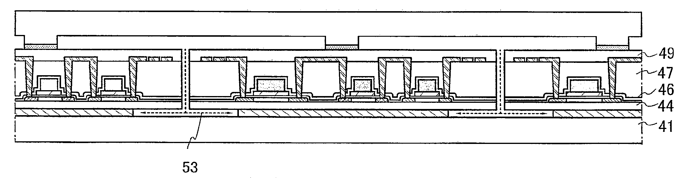
본 발명에 따른 박막집적회로 장치 및 그 제조 방법에 대해서, 도 1a 내지 1c, 도 2a 내지 2c, 도 3a 및 3b를 참조해서 설명한다. 우선, 기판(41) 위에, 박리층(43)을 형성한다. 여기에서는, 500nm 막 두께의 a-Si막(아모포스 실리콘막)을 스퍼터링법에 의해 형성했다. 기판으로는, 석영기판 이외에도, 유리 기판, 알루미나 등 절연 물질로 형성된 기판, 실리콘 웨이퍼 기판, 후공정의 처리 온도를 견디어낼 수 있는 내열성을 가지는 플라스틱 기판 등을 사용할 수 있다. 이 경우, 산화규소(SiOx), 질화규소(SiNx), 산화질화규소(SiOxNy)(x>y), 질화산화규소(SiNxOy)(x>y)(x, y=1, 2 ...)등, 기판으로부터 불순물 등의 확산을 방지하기 위한 하지 절연막을 형성할 수 있다. 또한 스테인레스 등의 금속 또는 반도체기판 등의 표면에 산화 실리콘이나 질화 실리콘 등의 절연막을 형성한 기판 등도 사용할 수 있다.A thin film integrated circuit device and a method of manufacturing the same according to the present invention will be described with reference to FIGS. 1A to 1C, 2A to 2C, 3A, and 3B. First, the
박리층(43)으로는, 아모포스 실리콘 이외에, 다결정 실리콘, 단결정 실리콘, 또는 세미 아모포스 실리콘(SAS, 미결정 실리콘) 등, 실리콘을 주성분으로 하는 층을 사용할 수 있다. 이들 박리층(43)은, 스퍼터링법 이외에도, 플라즈마CVD법 등에 의해 형성해도 된다. 박리층은 500nm 보다도 얇게 형성해도 된다.As the
다음으로 박리층(43) 위에, 하지막(44)을 형성한다. 여기에서는, 100nm 막 두께의 SiO2막을 스퍼터링법에 의해 형성했다. 하지막(44)은 ClF3 등의 할로겐화 불소에 의한 에칭으로부터 박막집적회로를 보호하는 역할을 한다. 따라서 이 기능을 가지는 한, 다른 재료를 사용해도 된다. 예를 들면 질화규소, 산질화규소 등을 사용할 수 있다. 또는, 상기 재료로 이루어지는 막을 적층해서 하지막(44)을 형성해도 된다. 하지막(44)은 스퍼터링법 대신에, 플라즈마CVD법 등으로 형성해도 된다.Next, the
다음으로 하지막(44) 위에 박막 트랜지스터(TFT), 유기TFT, 박막 다이오드 등을 형성하여 박막집적회로(42)를 형성한다. 도 1a는 채널 영역(35), 불순물 영역(36), 게이트 절연막(37), 게이트 전극(38)이 하지막(44) 위에 형성된 박막 트랜지스터로 형성된 박막집적회로(42)를 나타낸다. 본 실시 형태에서는 톱 게이트 구조를 이용했다. 그러나 그 대신에 보톰 게이트(역 스태거) 구조를 이용할 수 있다. 또한 박막 트랜지스터 대신에 유기TFT 또는 박막 다이오드를 사용할 수 있다. 이들 반도체 소자가 박막집적회로 장치의 CPU나 메모리 등을 구성한다. TFT를 사용한 CPU나 메모리 등의 박막집적회로의 제조 방법의 구체적인 예에 대해서는, 후술한다. 박막집적회로 장치는, 도 18에 나타낸 바와 같이 전원회로, 입출력 회로, 논리회로, CPU, 메모리를 포함한다. 여기에서는, TFT를 사용한 CPU(33)와, 메모리(34)만을 도시했다.Next, a thin film transistor (TFT), an organic TFT, a thin film diode, or the like is formed on the
다음으로 박막집적회로 소자를 보호하기 위해서, 제1의 층간 절연막(46)을 형성한다. 여기에서는, 질화규소막을 플라즈마CVD법에 의해 형성했지만, 제1의 층간 절연막(46)은 이 막에 한정되지 않는다. 또한, 제2의 층간 절연막(47)을 형성하는데 이는, 박막집적회로로 인한 불균질을 평탄화하기 위함이다. 폴리이미드, 아크릴, 폴리아미드나, 실록산 등의 내열성 유기수지를, 스핀 코트법, 딥법, 스프레이법, 액적토출법 등에 의해 형성할 수 있다. 그 대신에 무기재료를 사용해도 되는데, 그때는, PSG(인 글래스), BPSG(인 보론 글래스), 또는 알루미나막 등을 사용할 수 있다.Next, in order to protect the thin film integrated circuit device, the first
다음으로 레지스트를 마스크로 해서 컨택트 홀을 에칭 형성하고, 박막집적회로를 서로 접속하는 배선(45) 및 안테나(48)를 형성했다. 도전 재료로는, Ag, Au, Al, Cu, Zn, Sn, Ni, Cr, Fe, Co, Ti, 및 그 원소를 포함하는 합금을 사용할 수 있다. 그러나 도전 재료가 그것에 한정되는 것은 아니다. 또한 배선(45) 및 안테나(48)를 다른 재료로 형성해도 된다. 배선(45) 및 안테나(48)는 전성과 연성을 가지는 금속 재료를 포함하도록 형성하고, 바람직하게는 막 두께를 변형에 의한 응력을 견디도록 두껍게 한다.Next, contact holes were etched and formed using the resist as a mask, and wirings 45 and
배선(45) 및 안테나(48)는 스퍼터링에 의한 전체적인 성막 후, 레지스트 마스크를 사용한 패터닝에 의해 형성할 수 있다. 또는 배선(45) 및 안테나(48)를 노즐을 사용한 액적토출법에 의해 선택적으로 형성할 수 있다. 여기에서 하는 액적토출법에는, 잉크젯법뿐만 아니라, 오프셋법이나 스크린 인쇄 등도 포함된다.The
박막집적회로 장치를 내장하는 제품이, 도전 재료를 포함할 경우에는, 그것과 같은 도전 재료를 사용한 안테나 또는 배선을 형성해도 된다. 예를 들면 동전의 재료를 사용해서 동전의 내부에 안테나를 형성할 수 있다. 이 경우, 예를 들면 10엔 동전에 박막집적회로 장치를 매립할 경우에는, 동, 아연, 주석의 합금으로 된 안테나를 형성할 수 있다.When the product incorporating a thin film integrated circuit device contains a conductive material, an antenna or wiring using the same conductive material may be formed. For example, the material of a coin can be used to form an antenna inside the coin. In this case, for example, when the thin film integrated circuit device is embedded in a 10 yen coin, an antenna made of an alloy of copper, zinc and tin can be formed.
다음으로 안테나 위에, 보호막(49)을 형성한다. 보호막(49)으로는, DLC(다이아몬드 라이크 카본) 또는 질화탄소(CN) 등의 탄소를 가지는 막, 또는 질화규소막 또는 질화산화규소막 등을 사용할 수 있다. 또는, 폴리이미드, 아크릴, 폴리아미드나, 실록산 등의 내열성 유기수지를 사용할 수 있고, 무기재료를 사용해도 되는데, 그때는 PSG(인글래스), BPSG(인 보론 글래스), 알루미나막 등을 사용할 수 있다. 물론 보호막(49)으로 에폭시 수지를 사용할 수 있다. 이것들의 절연막을 적층시켜서, 보호막을 형성할 수 있다.Next, a
또한, 여기에서는, 박막집적회로 위에, 제1의 층간 절연막(46), 제2의 층간 절연막(47), 보호막(49)의 세 개의 절연막을 형성했다. 그것들의 재료는, 서로 교체해서 사용할 수 있다. 또는 제1 및 제2의 층간 절연막을 겸하여, 한 층의 층간 절연막으로 해도 된다. 어떠한 경우라도, 이들 절연막에 사용할 수 있는 재료로는, 후의 ClF3(삼불화염소) 등의 할로겐화 불소에 의한 에칭에 의해 손상되지 않는, 내열성이 있는 재료를 사용하는 것이 바람직하다(이상, 도 1b).In addition, three insulating films of the first
층간 절연막(46, 47)이나 보호막(49)으로는, 탄성이 높은 유기재료를 사용하는 것이 바람직하다. 이에 따라 변형시의 응력은, 유기재료를 가지는 층간 절연막이나 보호막에 집중되어, 주로 이들 막이 변형된다. 따라서 박막 트랜지스터에 작용하는 응력이 저감된다. 또 변형이 생길 경우에, 가장 응력이 부하되는 부분(에지, 모퉁이)이, 반도체막의 에지가 아닌 하지막의 에지가 되므로, 반도체막의 에지나 계면에서 생기는 응력 집중을 억제할 수 있다.As the
다음으로 박막집적회로 장치(50)의 경계 영역에, 다이싱에 의해 홈(93)을 형성한다(도 1b). 이때, 다이싱 장치(다이서)를 사용하는 블레이드 다이싱법을 이용하는 것이 일반적이다. 블레이드는, 다이아몬드 연마용 입자를 매립한 숫돌로, 그 폭는 약 30 ~ 50μm이다. 이 블레이드를 고속회전시킴으로써, 박막집적회로를 분리한다. 또한 다이싱에 필요한 에어리어를 스트리트라고 부르지만, 이 폭은, 소자의 손상을 고려하여, 80 ~ 150μm로 하는 것이 바람직하다.Next,
다이싱 이외에도, 스크라이빙 또는 마스크를 이용한 에칭 등에 의해 행할 수 있다. 스크라이빙의 경우에는, 다이아몬드 스크라이빙법과 레이저 스크라이빙법 등이 있다. 에칭의 경우에는, 노광, 현상 공정에 의해 마스크 패턴을 형성하고, 드라이에칭, 습식에칭 등에 의해 소자를 분리할 수 있다. 드라이에칭에 있어서는, 대기압 플라즈마법을 이용할 수 있다.In addition to dicing, it can be performed by scribing or etching using a mask. In the case of scribing, there are a diamond scribing method and a laser scribing method. In the case of etching, a mask pattern is formed by exposure and a development process, and an element can be isolate | separated by dry etching, wet etching, etc. In dry etching, an atmospheric pressure plasma method can be used.
홈을 형성할 경우, 홈의 깊이는, 적어도 박리층의 표면이 노출하는 정도면 되고, 기판(41)을 다시 사용할 수 있도록, 기판에 흠이 가지 않도록 상기 다이싱 등을 적절히 제어하는 것이 바람직하다.In the case of forming the groove, the depth of the groove should be at least as long as the surface of the release layer is exposed, and it is preferable to appropriately control the dicing or the like so that the substrate does not have a flaw so that the
다음으로 돌기부(58)를 가지는 지그(지지 기판)(52)를, 임시 접착제(51)를 매개로, 박막집적회로 장치(50) 각각에 부착하여 고정한다. 여기에서, 지그는, 박리층을 제거한 후에 박막집적회로가 따로따로 분리되지 않도록, 일시적으로 박막집적회로를 고정하는 역할을 한다. 지그의 형상으로는, 도 1c과 같이, 나중에 할로겐화 불소를 포함하는 기체 또는 액체의 도입을 쉽게 하기 위해서, 돌기부를 설치한 빗형 구조로 하는 것이 바람직하다. 하지만, 도 4c와 같이 평탄한 지그를 사용해도 된다. 돌기부를 가지는 지그(지지 기판)를 사용할 경우에는, 기판을 패터닝해서 사용할 수 있다. 지그로는, 할로겐화 불소에 의해 손상되지 않는 산화규소를 주성분으로 하는 유리기판, 석영기판, 스테인레스(SUS)기판 등을 사용할 수 있다. 할로겐화 불소에 의해 손상되지 않는 재료라면, 이것들에 한정되지 않는다. 또한 지그와 박막집적회로 사이에는, 임시 접착하기 위한 접착제가 설치된다.Next, the jig (supporting substrate) 52 having the
여기에서, 접착제로는, UV 광 조사에 의해 접착력(점착력)이 저하 또는 상실되지 않는 재료를 사용할 수 있다. 여기에서는, 니토 덴코 제품 UV 조사 박리 테이프를 사용했다. 이외에도, 3M사 제품의 포스트잇(등록상표)이나, 무어사 제품의 NOTESTIX(등록상표) 등에 사용할 수 있는 재박리 재접착 가능 접착제를 사용해도 된다. 예를 들면 일본국 공개특허공보 특개 2001-30403, 특허 2992092, 일본국 공개특허공보 특개 평6-299127에 기재된, 아크릴계 점착제, 합성고무계 점착제, 천연고무계 점착제 등을 사용할 수 있다. 지그를 간단히 뗄 수 있는 재료이면, 이것들에 한정되지 않는다.Here, as an adhesive agent, the material which adhesive force (adhesive force) does not fall or lose by UV light irradiation can be used. Here, the Nitto Denko UV irradiation peeling tape was used. In addition, you may use the re-peelable re-adhesive adhesive which can be used for the post-it (trademark) of 3M company, NOTESTIX (trademark) of a Moore company. For example, an acrylic adhesive, a synthetic rubber adhesive, a natural rubber adhesive etc. which are described in Unexamined-Japanese-Patent No. 2001-30403, patent 2992092, and Unexamined-Japanese-Patent No. 6-299127 can be used. It will not be limited to these as long as it is a material which can remove a jig easily.
다음으로 홈(93)에 할로겐화 불소 가스를 도입함으로써, 박리층(43)인 a-Si막을 에칭 제거했다(도 2a). 여기에서 쓰인 감압 CVD장치(도 12)에서는 ClF3 등의 할로겐화불소 가스(53)가 반응계인 벨자(89)에 도입되어 가스가 기판(90)에 확산된다. 또한 히터(91)가 벨자(89) 외부에 도입되고, 남아있는 가스가 배기관(92)으로부터 배기된다. 여기에서는, 도 12에 나타낸 바와 같은 감압 CVD장치를 사용하여, 가스: ClF3, 온도: 350℃, 유량: 300sccm, 기압: 6Torr, 시간: 3h의 조건으로 행한다. 그러나, 이 조건에 한정되는 것은 아니다. 또는 ClF3 가스에 질소를 섞은 가스를 사용해도 된다. 이 경우 두 가스의 유량비는 적절히 설정할 수 있다.Next, the a-Si film which is the
여기에서, ClF3 등의 할로겐화 불소는, 규소를 선택적으로 에칭한다는 특성이 있는 반면, 산화규소(SiOx), 질화규소(SiNx), 산질화규소(SiOxNy(x>y) 또는 SiNxOy(x>y))는 대부분 에칭되지 않는다. 따라서, 시간의 경과와 함께 박리층(43)이 에칭되어, 최종적으로 기판(41)을 박리할 수 있다(도 2b). 한편, 산화규소, 질화규소, 산질화규소 등이나, 내열성 수지로 이루어지는 하지막이나, 층간 절연막, 보호막은 대부분 에칭되지 않으므로, 박막집적회로의 손상을 방지할 수 있다. 박리한 기판(41)은 물론 재이용할 수 있어, 비용 삭감으로 이어진다.Here, halogenated fluorine such as ClF 3 has the property of selectively etching silicon, while silicon oxide (SiOx), silicon nitride (SiNx), silicon oxynitride (SiOxNy (x> y) or SiNxOy (x> y)) Is not etched mostly. Therefore, the
다음으로 UV 광 조사를 행하여, 임시 접착제(51)의 접착력을 저하 또는 상실시켜, 지그와, 박막집적회로 장치를 분리한다. 이는 박막집적회로 장치를 대량으로 제조할 수 있게 한다. 또한, 지그는, 비용 삭감을 위해, 재이용하는 것이 바람직하다.Next, UV light is irradiated to lower or lose the adhesive force of the temporary adhesive 51 to separate the jig and the thin film integrated circuit device. This makes it possible to manufacture a thin film integrated circuit device in large quantities. In addition, it is preferable to reuse a jig for cost reduction.
상기 방법에 의해 제조된 박막집적회로 장치(50)는, 소형 진공 핀셋(13) 등에 의해, 반송하고, 원하는 제품에 부착할 수 있다. 도 3a 및 3b는 제품(10)에 첨부되는 ID 라벨(15)의 제조 방법을 나타낸 것이다. 라벨(11)에 박막집적회로 장치(50)를 소형 진공 핀셋(13)으로 점착하고, 접착제(14)로 밀봉하여, ID 라벨(15)을 완성한다. 또한, 제품(10)에 ID 라벨(15)을 부착하여, 리더/라이터 등에 의해 정보를 인식, 갱신, 관리할 수 있는 제품이 완성된다.The thin film integrated
[실시 형태 2]Embodiment 2
본 실시 형태에서는 홈(93)을 형성하는 데 있어서, 드라이에칭법을 이용할 경우에 대해서, 도 4a 내지 4c를 이용하여 설명한다. 도 1a에 나타낸 보호막(49)의 형성까지는 실시 형태 1에 따라 실시했다. 그 후에 현상, 노광 공정을 거쳐, 기판 위에 레지스트(54)를 형성하고, 레지스트(54)를 마스크로 해서, 드라이에칭에 의해 홈(93)을 형성하고, 소자분리를 행한다(도 4a). 여기에서는, 플라스마 에칭을 채용하고, 에칭용 가스로는, Cl2, BCl3, SiCl4 혹은 CCl4 등을 대표로 하는 염소계 가스, CF4, SF8, NF3, CHF3 등을 대표로 하는 불소계 가스, 혹은 02을 사용했지만, 이것들에 한정되는 것은 아니다. 상기 에칭에는 대기압 플라즈마를 이용할 수도 있다. 이때, 에칭 가스로는 CF4과 02의 혼합 가스를 사용하는 것이 바람직하다. 또는 다른 종류의 가스를 사용하여 여러 번 에칭함으로써 홈(93)을 형성해도 된다.In this embodiment, the case where the dry etching method is used in forming the
다음으로 임시 접착제(51)를 매개로, 지그(55)를 박막집적회로 장치(50)에 부착하고, ClF3 등의 할로겐화 불소에 의해, 박리층을 제거하여, 최종적으로 기판(41)을 박리했다(도 4b). 박리층(43)을 제거하는 구체적인 방법은, 실시 형태 1과 같다. 지그(55)로서, 여기에서는, 돌기부를 특별히 설치하지 않은 기판을 사용했다. 물론, 돌기부를 가진 기판을 사용해도 된다.Next, the
다음으로 UV 광 조사를 행함으로써, 임시 접착제(51)의 접착력을 저하 또는 상실시켜, 지그(55)와, 박막집적회로 장치를 분리한다(도 4c). 이는 박막집적회로 장치를 대량으로 제조할 수 있게 한다. 상기 방법에 의해 제조된 박막집적회로 장치(50)를 소형 진공 핀셋 등에 의해, 반송하고, 원하는 제품에 부착할 수 있다.Next, by irradiating with UV light, the adhesive force of the
[실시 형태 3]Embodiment 3
다이싱 등에 의해 홈(93)을 형성할 때에, 기판(41)에 흠집이 생긴 경우, 그 기판을 재이용할 경우에 관하여, 도 5a 및 5b, 도 6a 내지 6c를 참조하여 설명한다. When scratches are formed on the
우선, 도 5a에 나타낸 바와 같이 사용 완료 기판(56) 위에 평탄화막(57)을 형성한다. 평탄화막(57)으로는, 폴리이미드, 아크릴, 폴리아미드나, 실록산 등의 내열성 수지를, 스핀 코트법, 딥법, 스프레이법, 액적토출법 등에 의해 형성할 수 있다. 후공정의 열처리를 고려하면, 실록산 등의 내열성 수지를 사용하는 것이 바람직하다. 또한 무기재료를 사용해도 되는데, 그때는, PSG(인 글래스), BPSG(인 보론 글래스), 알루미나 등을 사용할 수 있다. 그 후의 공정은 박막집적회로가 형성되고 분리되어 원하는 제품에 부착되는 실시 형태 1 또는 2와 동일하다.First, as shown in FIG. 5A, the
또 다른 방법으로서, 도 6a 내지 6c에 나타낸 바와 같이 CMP(화학적 기계적 연마)법, 프레싱, 에칭 백 등을 이용하여, 기판 표면을 평탄화하는 방법이 있는데, 사용이 끝난 기판(56)의 흠집이 미세할 때에는 CMP의 경우가 특히 효과적이다(도 6a). CMP법은, 연마용 패드(308)에 슬러리(307)라고 불리는 연마 용제를 공급하고, 웨이퍼 캐리어(306)의 회전과 플래튼이라고 불리는 회전대의 회전에 의한 가압과, 연마용 패드(308)의 연마에 의해 평탄화하는 것이다. 슬러리(307)로는 알카리성 콜로이드형 실리카를 섞은 것을 주로 사용할 수 있다. 프레싱의 경우(도 6b), 히터(301) 등의 가열 장치를 갖춘 장치(300)가 프레싱을 실행하는 데 바람직하게 쓰인다. 에칭 백에 있어서는(도 6c), 절연막(309)을 평탄하게 형성한 후, 평탄화를 위해 에칭을 한다. 다음 공정에서는, 실시 형태 1 또는 2와 같이, 박막집적회로 장치를 형성하고, 서로 분리하여, 원하는 제품에 부착할 수 있다.As another method, as shown in Figs. 6A to 6C, there is a method of planarizing the surface of the substrate by using CMP (Chemical Mechanical Polishing), pressing, etching back, or the like, where the scratches of the used
[실시 형태 4]Embodiment 4
상기 실시 형태에서는 박막집적회로의 제조 공정에서, 안테나를 형성했다. 본 실시 형태에서는 기판 위에 제조된 안테나와, 복수의 박막집적회로로 이루어진 집적회로를 각각 제조하고, 그 후 둘을 접속하는 방법에 대해서, 도 7a 내지 7c, 도 8a 내지 8e, 도 9a 및 9b, 도 10a 및 10b를 참조해서 설명한다.In the said embodiment, the antenna was formed in the manufacturing process of a thin film integrated circuit. In the present embodiment, an antenna fabricated on a substrate and an integrated circuit composed of a plurality of thin film integrated circuits are manufactured , respectively , and then connected to each other , and FIGS. 7A to 7C, 8A to 8E, 9A and 9B, It demonstrates with reference to FIG. 10A and 10B.
제1의 방법은, 도 7a에 나타낸 바와 같이, 구부릴 수 있는 플렉시블 기판(69) 위에, 안테나(68)를 형성하고, 별도 형성한 집적회로(25)를 도 7b에 나타낸 안테나의 접속부(99)에 접속한 후에, 플렉시블 기판(69)을 반으로 접고, 밀봉해서 도 7b에 나타내는 박막집적회로 장치를 제조하는 것이다. 안테나(68)는 스퍼터링법 등에 의해 형성한 후에 패터닝 형성해도 되고, 액적토출법을 이용하여, 도전 재료를 포함하는 조성물을 선택적으로 토출한 후에, 상기 조성물을 건조, 소성함으로써 형성해도 된다.In the first method, as shown in FIG. 7A, the
안테나를 형성한 후에, 도 6a 내지 6c에 나타낸, CMP법, 프레싱법, 에칭 백법 등에 의해, 평탄화를 향상시킬 수 있다. CMP법의 경우에는, 안테나는 도전성 재료로 이루어지므로, 슬러리로는, 산성용액에 알루미나의 분말을 섞은 것을 사용하는 것이 바람직하다. 프레싱법의 경우에는, 히터(301) 등의 가열기구를 구비한 장치에 의해 프레싱을 행하는 것이 바람직하다. 에칭 백에서는, 절연막(309)을 평탄하게 형성한 후에, 에칭을 행하여, 평탄화하는 것이다. 이러한 평탄화 처리 공정은, 박막집적회로의 제조 공정에서 이용할 수도 있다.After the antenna is formed, planarization can be improved by the CMP method, the pressing method, the etching back method, and the like shown in Figs. 6A to 6C. In the case of the CMP method, since the antenna is made of a conductive material, it is preferable to use a mixture of alumina powder with an acidic solution as the slurry. In the case of the pressing method, it is preferable to perform pressing by the apparatus provided with heating mechanisms, such as the
안테나에는, 안테나끼리 접속하는 접속부(98)나, 안테나와 집적회로를 접속하는 접속부(99)를, 안테나 형성시에 형성해도 된다. 또한 박막집적회로에 접속된 접속부(99)는, 안테나를 형성한 후에, 안테나의 일부를 절단함으로써 형성해도 된다. 집적회로와 안테나와의 접속은, 이방성 도전막이나, 공지의 본딩법 등을 이용하여 행할 수 있다. 안테나의 형상은, 접었을 때에 대칭이고 코일형이면, 도 7a 내지 7c에 나타내는 형상에 한정되지 않는다.In the antenna, a connecting
안테나에 삽입되는 집적회로(25)는, 도 18에 나타낸 바와 같이 전원회로(26), 입출력 회로(27), 논리회로(28), 메모리(29), CPU(30) 등에, 리더/라이터(136)와 전파를 주고받는 안테나 회로가 접속된 구성을 가진다.As shown in FIG. 18, the
도 8a 내지 8e는, 도 7c의 X-Y 단면에서 본 안테나 기판의 접힌 상태를 나타낸 도면이다. 안테나(20)를 패터닝 형성할 때에 사용한 레지스트(23)를 애싱 등에 의해 제거하지 않고, 잔존시켰다. 또한, 평탄화막(60)을 스핀 코트법, 딥법, 스프레이법, 액적토출법 등에 의해 형성하고, 평탄화를 행했다(도 8b). 집적회로(25)(IC칩)와의 접속부를 확보하기 위해서, 레지스트(61)를 마스크로 해서, 에칭 또는 애싱을 행하여, 콘택트부(62)를 형성했다(도 8c). 또한, 이방성 도전막(63)을 사이에 두고 집적회로(25)를 형성하고, 실링제(64)를 사이에 두고, 안테나가 형성된 플렉시블 기판(19)을 접어(도 8d), 박막집적회로 장치(66)를 완성했다(도 8e). 이 경우, 대향하는 안테나 사이에 배선 등을 설치해서 안테나끼리 접속해도 된다. 레지스트(23)나 평탄화막(60)은, 기판을 접었을 때에, 안테나나 집적회로를 보호하는 쿠션의 역할을 한다. 레지스트(23)나 평탄화막(60)은, 한쪽 또는 양쪽을 생략할 수도 있다.8A to 8E are diagrams showing a folded state of the antenna substrate seen from the X-Y cross section of FIG. 7C. The resist 23 used when patterning the
제2의 방법은, 도 9a 및 9b에 나타낸 바와 같이 기판(69) 위에 안테나(68)를 복수 형성해 두고, 기판(69)을 다이싱 등에 의해 잘라내고, 안테나 기판 사이에 집적회로(25)를 끼우는 방법이다. 접속부(21)는 안테나끼리 접속하기 위해서 사용해도 되고, 집적회로와 안테나를 접속하는 데 사용해도 된다. 또한 접속부(21)는 안테나의 다른 위치에 형성해도 된다. 기판끼리 서로 부착할 때, 얼라인먼트 마커를 설치할 필요가 있는데, 상기 접속부(21)를 마커로 사용할 수 있다.In the second method, as shown in Figs. 9A and 9B, a plurality of
제3의 방법은, 도 10a 또는 10b에 나타낸 바와 같이, 두 쪽이 닫힌 식품을 포장하는 랩 형태의 플렉시블 기판(70)이나(도 10a), 세 쪽이 닫힌 봉투형 플렉시블 기판(74)에(도 10b), 안테나(71)를 양면에 형성해 두고, 그 사이에 집적회로(25)(IC칩)를 삽입하고, 접착제(73)로 밀봉하는 방법이다. 접속부(21)는 개공이므로, 안테나끼리, 또는 안테나와 집적회로가 접속할 수 있다. IC칩은 소형 진공 핀셋 등으로 설치하면 된다. 안테나는 이들 기판의 내측 표면에 형성해도 된다.In the third method, as shown in FIG. 10A or 10B, a wrap-type
본 실시 형태에서 서술한 박막집적회로 장치의 제조 방법은, 특히, 안테나 기판과, 집적회로(IC칩)를 별도의 제조자가 제조하고, 중간 생성품(부품)으로서 유통시킬 경우에 적합한 방법이다.The manufacturing method of the thin film integrated circuit device described in this embodiment is a method particularly suitable when a separate manufacturer manufactures an antenna substrate and an integrated circuit (IC chip) and distributes it as an intermediate product (component).
[실시 형태 5][Embodiment 5]
본 실시 형태에서는 도 11a 내지 11c를 참조하여, 소자 기판(75)에 임시 접착한 지그(76)를 떼지 않고, 직접, 제품(84) 등에 접착하는 방법에 관하여 설명한다. 우선, 실시 형태 1 ~ 3에 기초하여, 소자 기판(75)을 형성하고, 임시 접착제(81)를 매개로 지그를 부착한다. 지그(76)로는, 도 11a 및 11b에 나타낸 바와 같이 돌기부(77)를 가지는 지그를 사용했다. 임시 접착제(81)로는, 여기에서는, UV 광 조사에 의해 접착력이 저하 또는 상실되는 재료를 사용한다. 또한 소자의 손상을 막기 위해서, 유기재료 또는 무기재료로 된 층간막(79)을 설치한다. 그리고, ClF3 등의 할로겐화 불소에 의한 에칭에 의해, 소자 분리를 행한다.In this embodiment, with reference to FIGS. 11A-11C, the method of directly sticking to the
다음으로 지그(76)에 소자가 임시 접착된 상태에서 반송하고, ID 카드 등의 제품이 설치된 스테이지와의 얼라인먼트를 행한다. 이때, 도 11a에 나타낸 바와 같이 지그나, 스테이지에 설치된 얼라인먼트 마커를 이용할 수도 있고, 도면에는 나타내지 않았지만, 제품(84)에 형성된 마커를 이용할 수도 있다. 제품(84) 내의 박막집적회로 장치가 형성되는 부분에는, 미리 접착제(85)가 형성되어 있고, 지그를 제어함으로써, 원하는 소자를 제품(84)의 원하는 위치에 부착한다(도 11a).Next, the device is conveyed in a state where the element is temporarily bonded to the
다음으로 제품(84)에 부착하고자 하는 소자에, 마스크를 통해 UV광(86)을 선택적으로 조사하고, 임시 접착제(81)의 접착력을 저하 또는 상실시킴으로써, 지그를 소자를 분리한다(도 11b). 이에 따라 원하는 소자(집적회로(87))를 제품의 원하는 위치에 형성할 수 있다. 소자 형성 후, 예를 들면 커버(88)로, 소자부를 커버한다(도 11c). 여기에서는, 제품의 내부에 안테나(83)가 형성된 경우를 나타냈지만, 소자부에 안테나를 형성해도 된다.Next, the device to be attached to the
본 실시 형태에 나타낸 본 발명을 사용함으로써, ClF3 등의 할로겐화 불소에 의한 에칭에 의해 소자 분리를 행했을 때, 소자가 따로따로 분리되지 않고, 원하는 소자를 원하는 위치에 형성할 수 있다.By using the present invention shown in the present embodiment, when the element is separated by etching with halogenated fluorine such as ClF 3 , the element is not separated separately and a desired element can be formed at a desired position.
[실시예 1]Example 1
본 실시예에서는, 도 13a 내지 13e, 14a 내지 14e를 참조하여, 박막집적회로 장치의 집적회로부의 구체적인 제조 방법에 관하여 설명한다. 여기에서는, 간략화를 위해, n형 TFT와 p형 TFT를 사용한 CPU와 메모리의 제조 방법에 관하여 설명한다.In the present embodiment, with reference to Figs. 13A to 13E and 14A to 14E, a specific manufacturing method of the integrated circuit portion of the thin film integrated circuit device will be described. Here, for the sake of simplicity, a description will be given of a method of manufacturing a CPU and a memory using an n-type TFT and a p-type TFT.
우선, 기판(41) 위에, 박리층(43)과, 하지막(44)을 형성한다(도 13a). 이들 기판(41), 박리층(43), 하지막(44)을 형성하기 위한 재료나 제조 방법으로는, 상기 실시 형태 1 내지 5에 서술한 재료나 제조 방법을 채용할 수 있다.First, the
다음으로 하지막(44) 위에, 섬 형상 반도체막(100)을 형성한다. 섬 형상 반도체막(100)은 아모포스 반도체, 결정성 반도체, 또는 세미 아모포스 반도체로 형성한다. 모두, 실리콘, 실리콘-게르마늄(SiGe) 등을 주성분으로 하는 반도체막을 사용할 수 있다.Next, the island-
여기에서는, 70nm의 막 두께의 아모포스 실리콘을 형성하고, 또한 그 표면을, 니켈을 포함하는 용액으로 처리한 후, 500 ~ 750℃의 열결정화 공정에 의해 결정질 실리콘 반도체막을 얻고, 또한 레이저 결정화를 행해서 결정성을 개선했다. 아모포스 실리콘막의 성막 방법으로는, 플라즈마CVD법, 스퍼터링법, LPCVD법 등을 이용할 수 있다. 결정화 방법으로는, 레이저결정화법, 열결정화법, 다른 촉매(Fe, Ru, Rh, Pd, Pd, Os, Ir, Pt, Cu, Au 등)를 사용한 열결정화, 또는 그것들을 교대로 복수 회 행해도 된다.Here, after forming amorphous silicon with a film thickness of 70 nm, and treating the surface with the solution containing nickel, a crystalline silicon semiconductor film is obtained by the 500-750 degreeC thermal crystallization process, and also laser crystallization is performed. The crystallinity was improved. As the method for forming the amorphous silicon film, a plasma CVD method, a sputtering method, an LPCVD method, or the like can be used. As the crystallization method, the laser crystallization method, the thermal crystallization method, thermal crystallization using other catalysts (Fe, Ru, Rh, Pd, Pd, Os, Ir, Pt, Cu, Au, etc.), or they may be alternately performed a plurality of times do.
아모포스 구조를 가지는 반도체막의 결정화 처리로는, 연속발진의 레이저를 사용할 수 있다. 결정화시에 큰 입경의 결정을 얻기 위해서는, 연속발진 고체레이저를 사용하고, 기본파의 제2 고조파 ~ 제4 고조파를 적용하는 것이 바람직하다. 대표적으로는, Nd:YVO4 레이저(기본파: 1064nm)의 제 2고조파(532nm)나 제 3고조파(355nm)를 적용하면 된다. 연속발진의 레이저를 사용할 경우에는, 출력 10W의 연속발진의 YVO4 레이저로부터 쏘아진 레이저광을 비선형 광학 소자에 의해 고조파로 변환한다. 공진기 내에 YVO4 결정과 비선형 광학 소자를 넣고, 고조파를 쏘는 방법도 있다. 그리고, 바람직하게는 광학계에 의해 사각형 또는 타원형의 레이저광으로 형성하고, 피처리 물체에 조사한다. 이때의 에너지밀도는 0.01 ~ 100MW/cm2 정도(바람직하게는 0.1 ~ 10MW/cm2)가 필요하다. 10 ~ 2000cm/s 정도의 속도로 레이저광에 대하여 상대적으로 반도체막을 이동시켜서 조사하면 된다.As crystallization of the semiconductor film having an amorphous structure, a laser of continuous oscillation can be used. In order to obtain a crystal having a large particle size at the time of crystallization, it is preferable to use the second to fourth harmonics of the fundamental wave using a continuous oscillation solid laser. Typically, the second harmonic wave (532 nm) or the third harmonic wave (355 nm) of the Nd: YVO 4 laser (fundamental wave: 1064 nm) may be applied. When using a laser of continuous oscillation, the laser beam shot from the YVO 4 laser of 10 W continuous oscillation is converted into harmonics by a nonlinear optical element. Another method is to put a YVO 4 crystal and a nonlinear optical element into the resonator and shoot harmonics. Then, it is preferably formed into a rectangular or elliptical laser light by an optical system and irradiated to the object to be processed. At this time, the energy density needs to be about 0.01 to 100MW / cm 2 (preferably 0.1 to 10MW / cm 2 ). What is necessary is just to irradiate by moving a semiconductor film relatively with respect to a laser beam at the speed of about 10-2000 cm / s.
상기 방법에 의해 결정성 실리콘 반도체막을 얻은 후, 반도체막 위에 산화막을 사이에 두고, 금속 촉매를 게터링하기 위한 아모포스 실리콘막을 성막하고, 500 ~ 750℃의 열처리에 의해 게터링 처리를 행했다. 또한, TFT의 역치 전압을 제어하기 위해서, 결정성 실리콘 반도체막에 대하여, 1013/cm2 오더의 도즈량의 붕소 이온을 주입했다. 그 후에 레지스트를 마스크로 해서 에칭함으로써, 섬 형상 반도체막(100)을 형성했다.After obtaining the crystalline silicon semiconductor film by the said method, the amorphous silicon film for gettering a metal catalyst was formed into a film on the semiconductor film between the oxide films, and the gettering process was performed by heat processing of 500-750 degreeC. In addition, in order to control the threshold voltage of the TFT, boron ions having a dose of 10 13 / cm 2 order were implanted into the crystalline silicon semiconductor film. Subsequently, the island-
결정성 반도체막을 형성하는 데 있어서는, 디실란(Si2H6)과 불화게르마늄(GeF4)을 원료 가스로 사용해서, LPCVD(감압CVD)법에 의해, 다결정 반도체막을 직접 형성함으로써도, 결정성 반도체막을 얻을 수 있다. 이 경우, 가스 유량비는, Si2H6/GeF4 = 20/0.9, 성막 온도는 400 ~ 500℃, 캐리어 가스로서 He 또는 Ar를 사용할 수 있다. 그러나, 이에 한정되지는 않는다.In forming a crystalline semiconductor film, the crystalline crystalline semiconductor film is also formed by directly forming a polycrystalline semiconductor film by LPCVD (decompression CVD) using disilane (Si 2 H 6 ) and germanium fluoride (GeF 4 ) as source materials. A semiconductor film can be obtained. In this case, as the gas flow rate ratio, Si 2 H 6 / GeF 4 = 20 / 0.9, the film formation temperature is 400 to 500 ° C, and He or Ar can be used as the carrier gas. However, it is not limited to this.
다음으로 게이트 전극 위에 게이트 절연막(102)을 형성한다(도 13b). 게이트 절연막(102)은 플라즈마CVD법 또는 스퍼터링법 등의 박막 형성법을 이용하여, 질화규소, 산화규소, 질화산화규소 또는 산화질화규소를 포함하는 막을, 단층으로, 또는 적층시켜서 형성하는 것이 바람직하다. 적층할 경우에는, 예를 들면 기판 측으로부터 산화규소막, 질화규소막, 산화규소막의 3층 구조로 하는 것이 바람직하다.Next, a
다음으로 게이트 전극(103)을 형성한다(도 13c). 여기에서는, 30nm의 막 두께의 TaN(질화탄탈)과, 370nm의 막 두께의 W(텅스텐)을 스퍼터링법에 의해 적층형성한 후에, 레지스트(104)를 마스크로 해서 에칭함으로써, 게이트 전극(103)을 형성했다. 여기에서, 레지스트 마스크의 대신에, SiOx 등의 마스크를 사용해도 된다. 이 경우, 산화규소, 산질화규소 등의 마스크(하드 마스크라고 불린다)를 패터닝 형성하는 공정이 부가된다. 그러나, 에칭시에 있어서의 마스크의 막 감소가 레지스트보다도 적으므로, 원하는 폭의 게이트 전극을 형성할 수 있다. 물론, 게이트 전극(103)의 재료, 구조, 제조 방법은, 이에 한정되지는 않고, 적절히 선택할 수 있다. 예를 들면 레지스트(104)를 사용하지 않고, 액적토출법을 이용해서 선택적으로 게이트 전극(103)을 형성해도 된다.Next, the
게이트 전극(103)을 형성하는 도전 재료로는, 도전막의 기능에 따라 여러 가지 재료를 선택할 수 있다. 대표적으로는, 은(Ag), 구리(Cu), 금(Au), 니켈(Ni), 백금(Pt), 크롬(Cr), 주석(Sn), 팔라듐(Pd), 이리듐(Ir), 로듐(Rh), 루테늄(Ru), 레늄(Re), 텅스텐(W), 알루미늄(Al), 탄탈(Ta), 인듐(In), 텔루르(Te), 몰리브덴(Mo), 카드뮴(Cd), 아연(Zn), 철(Fe), 티타늄(Ti), 실리콘(Si), 게르마늄(Ge), 지르코늄(Zr), 바륨(Ba), 안티몬납, 산화주석?안티몬, 불소 도프 산화아연, 탄소, 그래파이트, 글래시 카본, 리튬, 베릴륨, 나트륨, 마그네슘, 칼륨, 칼슘, 스칸듐, 망간, 지르코늄, 갈륨, 니오브, 나트륨-칼륨 합금, 마그네슘/구리 혼합물, 마그네슘/은 혼합물, 마그네슘/알루미늄 혼합물, 마그네슘/인듐 혼합물, 알루미늄/산화알류미늄 혼합물, 리튬/알루미늄 혼합물 등, 할로겐화은의 미립자 또는 분산성 나노 입자, 투명 도전막으로 사용할 수 있는 산화인듐주석(ITO), ITSO(규소 또는 산화규소를 포함하는 ITO), 산화아연(ZnO), 갈륨을 첨가한 산화아연(GZO), 산화인듐에 2 ~ 20%의 산화아연을 혼합한 산화인듐아연(IZO), 유기 인듐, 유기 주석, 질화티타늄 등을 적절히 채용할 수 있다.As the conductive material for forming the
게이트 전극(103)을 에칭 형성할 때의 에칭 가스로는 CF4/Cl2/O2의 혼합 가스나 Cl2 가스를 사용했다. 하지만, 에칭 가스가 이것에 한정되는 것은 아니다.As an etching gas when etching the
다음으로 p형 TFT(109, 111)가 되는 부분을 레지스트(118)로 덮고, 게이트 전극을 마스크로 해서, n형 TFT(1O8, 110)의 섬 형상 반도체막에, n형을 부여하는 불순물원소(119)(대표적으로는 P(인) 또는 As(비소))를 저농도로 도프한다(도 13d). 제1의 도핑 공정의 조건은, 도즈량: 1ㅧ1013 ~ 6ㅧ1013atom/cm2, 가속 전압: 50 ~ 70kV로 했지만, 이것에 한정되지 않는다. 이 제1의 도핑 공정에 의해, 게이트 절연막(102)을 통해 스루 도프가 행해지고, 여러 쌍의 저농도 불순물영역(120)이 형성된다. 제1의 도핑 공정은, p형 TFT 영역을 레지스트로 덮지 않고, 전체 면에 행해도 된다.Next, an impurity element for covering the portion to be the p-
다음으로 레지스트(118)를 애싱 등에 의해 제거한 후, n형 TFT영역을 덮는 레지스트(121)를 새롭게 형성하고, 게이트 전극을 마스크로 해서, p형 TFT(1O9, 111)가 되는 섬 형상 반도체막에, p형을 부여하는 불순물원소(122)(대표적으로는 B(붕소))를 고농도로 도프한다(도 13e). 제2의 도핑 공정의 조건은, 도즈량: 1ㅧ1016 ~ 3ㅧ1016atom/cm2, 가속 전압: 20 ~ 40kV로 해서 행한다. 이 제2의 도핑 공정에 의해, 게이트 절연막(102)을 통해 스루 도프가 이루어지고, 여러 쌍의 p형 고농도 불순물영역(123)이 형성된다.Next, after removing the resist 118 by ashing or the like, a resist 121 covering the n-type TFT region is newly formed, and the island-like semiconductor film that becomes the p-
다음으로 레지스트(121)를 애싱 등에 의해 제거한 후, 기판 표면에, 절연막(105)을 형성했다(도 14a). 여기에서는, 막 두께 100nm의 SiON(산질화규소)막과, 막 두께 200nm의 저온 산화막의 2층 구조로 했다. 여기에서는, SiON막은, 플라즈마CVD법로 형성하고, 저온 산화막은, SiO2막을 감압CVD법으로 형성했다. 그 후에 도시하지 않지만, 기판의 TFT가 형성된 측을 레지스트로 덮고, 기판의 이면에 형성된 절연막을 에칭 제거했다(이면 처리).Next, after removing the resist 121 by ashing or the like, an insulating
다음으로 레지스트를 남긴 상태로, 에칭 백법에 의해, 레지스트 및 절연막(105)을 에칭 제거하여, 사이드 월(106)을 자기정합적(셀프 어라인)으로 형성했다(도 14b). 에칭 가스로는, CHF3과 He의 혼합 가스를 사용했다. 사이드 월을 형성하는 공정은, 이것들에 한정되지 않는다.Next, the resist and the insulating
다음으로 p형 TFT영역을 덮는 레지스트(124)를 새롭게 형성하고, 게이트 전극(103) 및 사이드 월(106)을 마스크로 해서, n형 도전성을 부여하는 불순물원소(125)(대표적으로는 P(인) 또는 As(비소))를 고농도로 도프한다(제3의 도핑 공정, 도 14c). 제3의 도핑 공정의 조건은, 도즈량: 1ㅧ1013 ~ 5ㅧ1015atom/cm2, 가속 전압: 60 ~ 100kV로 행한다. 이 제3의 도핑 공정에 의해, 게이트 절연막(102)을 통해 스루 도프가 이루어지고, 여러 쌍의 n형 고농도 불순물영역(126)이 형성된다.Next, a resist 124 is formed to cover the p-type TFT region, and the impurity element 125 (typically P (p) which imparts n-type conductivity using the
도면에는 나타내지 않았지만, 레지스트(124)를 애싱 등에 의해 제거한 후, 불순물영역의 열활성화를 행해도 된다. 예를 들면 50nm의 SiON막을 성막한 후, 550℃, 4시간, 질소분위기 하에서, 가열처리를 행하면 된다. 또한 수소를 포함하는 SiNx막을, 100nm의 막 두께로 형성한 후, 410℃, 1시간, 질소분위기 하에서, 가열처리를 함으로써, 결정성 반도체막의 결함을 개선할 수 있다. 이것은, 예를 들면 결정성 실리콘 내에 존재하는 댕글링 본드를 종단시키는 것이며, 수소화 처리공정 등으로 불린다. 또한, 이 후, TFT를 보호하는 캡 절연막으로서, 막 두께 600nm의 SiON막을 형성한다. 수소화처리 공정은, 상기 SiON막 형성 후에 행해도 된다. 이 경우, SiNx\SiON막은 연속 성막할 수 있다. 이렇게, TFT 위에는, SiON\SiNx\SiON의 3층의 절연막이 형성되는 것이 되지만, 그 구조나 재료는 이것들에 한정되지 않는다. 또한 이들 절연막은, TFT를 보호하는 기능도 가지기 때문에, 가능한 한 형성해 두는 것이 바람직하다.Although not shown in the figure, the resist 124 may be removed by ashing or the like, followed by thermal activation of the impurity region. For example, after forming a 50-nm SiON film | membrane, you may heat-process in 550 degreeC and nitrogen atmosphere for 4 hours. In addition, after forming a SiNx film containing hydrogen at a thickness of 100 nm, the heat treatment is performed at 410 ° C. for 1 hour under a nitrogen atmosphere, whereby defects in the crystalline semiconductor film can be improved. This terminates the dangling bond which exists in crystalline silicon, for example, and is called a hydrogenation process etc. After that, a SiON film having a thickness of 600 nm is formed as a cap insulating film for protecting the TFT. The hydroprocessing step may be performed after the SiON film is formed. In this case, the SiNx\SiON film can be formed into a continuous film. In this way, an insulating film of three layers of SiON\SiNx\SiON is formed on the TFT, but the structure and the material are not limited to these. Moreover, since these insulating films also have a function of protecting the TFT, it is preferable to form them as much as possible.
다음으로 TFT 위에, 층간 절연막(107)을 형성한다. 층간 절연막(107)의 형성에는, 폴리이미드, 아크릴, 폴리아미드나, 실록산 등의 내열성 유기수지를 사용할 수 있다. 형성 방법으로는, 그 재료에 따라, 스핀 코트, 딥, 스프레이 도포, 액적토출법(잉크젯법, 스크린인쇄, 오프셋 등), 닥터 나이프, 롤 코터, 커튼 코터, 나이프 코터 등을 채용할 수 있다. 또한 무기재료를 사용해도 되는데, 그때는, PSG(인글래스), BPSG(인 보론 글래스), 알루미나막 등을 사용할 수 있다. 이들 절연막을 적층시켜서 층간 절연막(107)을 형성해도 된다.Next, an
다음으로 레지스트를 형성한 후, 에칭에 의해 컨택트 홀을 개공하고, 배선(128) 및 안테나(48)를 형성한다(도 14d). 컨택트 홀 개공시의 에칭에 사용할 수 있는 가스는, CHF3과 He의 혼합 가스를 사용했지만, 이것에 한정되지 않는다.Next, after forming a resist, a contact hole is opened by etching, and the
배선(128)과 안테나(48)는 동일 재료를 사용해서 동시에 형성해도 되고, 각각 형성해도 된다. 여기에서는, TFT와 접속되는 배선(128)은, Ti, TiN, Al-Si, TiN, Ti(이 순서로 적층)의 5층 구조로 해서 스퍼터링법에 의해서 형성한 후, 패터닝 형성했다.The
Al층에 있어서, Si를 혼입시킴으로써, 배선 패터닝 시의 레지스트 베이킹에 있어서의 힐록의 발생을 방지할 수 있다. 또한 Si 대신에, 0.5% 정도의 Cu를 혼입시켜도 된다. 또한 Ti나 TiN 사이에 Al-Si층을 샌드위치함으로써, 내(耐)힐록성이 더욱 향상한다. 패터닝시에는, SiON 등으로 된 상기 하드 마스크를 사용하는 것이 바람직하다. 배선의 재료나, 형성 방법은 이것들에 한정되지 않고, 전술한 게이트 전극에 사용할 수 있는 재료를 채용해도 된다. 안테나(48)를 형성할 때는, 상기 실시예에 나타낸, 여러 가지 재료, 방법을 이용할 수 있다. 배선과 안테나는, 동시에 형성해도 된고, 한쪽을 먼저 형성한 후에, 그 쪽에 다른 쪽이 겹치도록 형성해도 된다.By mixing Si in the Al layer, it is possible to prevent the occurrence of hillock in resist baking during wiring patterning. In addition, about 0.5% of Cu may be mixed instead of Si. In addition, by sandwiching the Al-Si layer between Ti and TiN, the heel resistance is further improved. At the time of patterning, it is preferable to use said hard mask made of SiON or the like. The material of wiring and the formation method are not limited to these, You may employ | adopt the material which can be used for the gate electrode mentioned above. When forming the
다음으로 배선 및 안테나 위에, 보호막(49)을 형성하여, CPU(33) 및 메모리(34)를 완성한다(도 14e). 보호막(49)으로는, DLC(다이아몬드 라이크 카본) 또는 질화탄소(CN) 등의 탄소를 가지는 막, 또는 질화규소막 또는 질화산화규소막 등을 사용할 수 있다. 형성 방법으로는, 플라즈마CVD법이나, 대기압 플라즈마 등을 이용할 수 있다.Next, the
혹은, 폴리이미드, 아크릴, 폴리아미드, 레지스트 물질의 벤조시클로부텐 등의 감광성 또는 비감광성 유기재료나, 실록산 등의 내열성 유기수지를 보호막(49)으로 사용할 수 있다. 형성 방법은 그 재료에 따라, 스핀 코트, 딥, 스프레이 도포, 액적토출법(잉크젯법, 스크린인쇄, 오프셋 등), 닥터 나이프, 롤 코터, 커튼 코터, 나이프 코터 등을 채용할 수 있다. 또는, 도포법에 의해 얻어지는 SOG막(예를 들면 알킬기를 포함하는 SiOx막)을 사용할 수도 있다. 또한 무기재료를 사용해도 되는데, 그때는, 산화규소, 질화규소, 산질화규소, PSG(인글래스), BPSG(인 보론 글래스), 알루미나 막 등을 사용할 수 있다. 상기 재료를 각각 포함하는 절연막을 적층시켜서, 보호막(49)을 형성해도 된다.Alternatively, a photosensitive or non-photosensitive organic material such as polyimide, acrylic, polyamide, or benzocyclobutene of a resist material, or a heat resistant organic resin such as siloxane can be used as the
그 후에 본 실시예에 의해 제조된 복수의 TFT는, 상기 실시예에 나타내는 방법으로 IC칩마다 분리되어, 제품 등에 내장할 수 있다. 본 실시예에서는, 톱 게이트 구조로 했지만, 보텀 게이트 구조(역 스태거 구조)로 해도 된다. 본 실시예는 상기 실시 형태 및 실시예와 자유롭게 조합할 수 있다.Thereafter, the plurality of TFTs manufactured according to the present embodiment can be separated for each IC chip by the method shown in the above embodiment and embedded in a product or the like. In the present embodiment, the top gate structure is used, but the bottom gate structure (inverse stagger structure) may be used. This example can be combined freely with the above embodiments and examples.
[실시예 2][Example 2]
본 실시예에서는, 실시예 1의 프로세스에 있어서, 고온 폴리실리콘(HPS)을 채용한 경우에 관하여 설명한다. 일반적으로, 유리 기판의 내열온도(약 600℃)이상의 결정화 프로세스를 포함하는 반도체 프로세스를, 고온 프로세스라고 부른다.In this embodiment, a case where high temperature polysilicon (HPS) is employed in the process of Example 1 will be described. Generally, the semiconductor process including the crystallization process of the heat resistant temperature (about 600 degreeC) or more of a glass substrate is called high temperature process.
반도체막을 형성한 후에, Ni, Fe, Ru, Rh, Pd, Os, Ir, Pt, Cu, Au 등의 상기 촉매를 첨가하고, LPCVD 노에서 가열처리를 행한다. 약 700℃ 이상에서, 반도체막 내에 결정 핵이 발생하고, 결정화가 진행된다.After the semiconductor film is formed, the above catalysts such as Ni, Fe, Ru, Rh, Pd, Os, Ir, Pt, Cu, Au, and the like are added, and heat treatment is performed in an LPCVD furnace. Above about 700 ° C, crystal nuclei are generated in the semiconductor film and crystallization proceeds.
그 후에 섬형 반도체막을 형성한 후, LPCVD에 의해, 게이트 절연막을 형성한다. 예를 들면, 실란계 가스에 N2나 02을 혼합시킨 가스를 사용하고, 900℃ 이상의 고온에서, HTO막(High Temperature Oxide)을 형성한다.After forming an island-like semiconductor film, a gate insulating film is formed by LPCVD. For example, a gas obtained by mixing N 2 or 0 2 with a silane gas is used to form an HTO film (High Temperature Oxide) at a high temperature of 900 ° C or higher.
다음으로 인 등의 n형 불순물을 포함하는 폴리실리콘(p-Si)을 150nm의 막 두께로 성막함으로써, 게이트 전극을 형성한다. 또한, W-Si(텅스텐 실리사이드)을 150nm의 막 두께로 성막해도 된다. 형성 방법으로는, 스퍼터링법, CVD법 등을 적절히 채용할 수 있다. 그 후의 도핑 공정은, 실시예 1과 마찬가지로 형성할 수 있다.Next, a polysilicon (p-Si) containing n-type impurities such as phosphorus is formed into a film with a thickness of 150 nm to form a gate electrode. Further, W-Si (tungsten silicide) may be formed into a film with a thickness of 150 nm. As a formation method, a sputtering method, a CVD method, etc. can be employ | adopted suitably. The subsequent doping process can be formed similarly to Example 1.
도핑 공정 후, 950℃, 30분의 열활성화를 행하여, 불순물영역을 활성화시킨다. 또한, BPSG(인 보론 글래스)을 사용해서 리플로우를 행하고, 레지스트를 사용한 에칭 백에 의해, 평탄화를 행한다. 또한, 350℃의 수소화 어닐을 행하여, 플라즈마 데미지를 회복시킨다.After the doping process, thermal activation at 950 ° C. for 30 minutes is performed to activate the impurity region. Furthermore, reflow is performed using BPSG (in boron glass), and planarization is performed by the etching back using a resist. In addition, hydrogenation annealing at 350 ° C. is performed to recover plasma damage.
기타의 공정은, 실시예 1과 마찬가지로 행할 수 있다. 본 실시예에서는, 톱 게이트 구조로 했지만, 보텀 게이트 구조(역 스태거 구조)로 해도 된다. 본 실시예는, 다른 실시 형태, 실시예와 자유롭게 조합할 수 있다.Other processes can be performed similarly to Example 1. In the present embodiment, the top gate structure is used, but the bottom gate structure (inverse stagger structure) may be used. This example can be combined freely with other embodiments and examples.
[실시예 3][Example 3]
본 실시예에서는, 실시예 1의 프로세스에 있어서, 섬 형상 반도체막(100)로서, SAS(세미 아모포스 실리콘)을 채용했을 경우에 관하여 설명한다. SAS는 규화물 기체를 글로 방전 분해하여 얻을 수 있다. 대표적인 규화물 기체로는, SiH4이며, 그 밖에도 Si2H6, SiH2Cl2, SiHCl3, SiCl4, SiF4 등을 사용할 수 있다. 이 규화물 기체를 수소, 수소와 헬륨, 아르곤, 크립톤, 네온으로 이루어진 그룹에서 선택된 일종 또는 복수 종의 희가스 원소로 희석해서 사용함으로써 SAS의 형성을 용이하게 할 수 있다. 희석율은 10배 ~ 1000배의 범위에서 규화물 기체를 희석하는 것이 바람직하다. 물론, 그로방전 분해에 의한 피막의 반응 생성은 감압 상태에서 행하지만, 압력은 대략 0.1Pa ~ 133Pa의 범위에서 행하면 된다. 그로방전을 형성하기 위한 전력은 1MHz ~ 120MHz, 바람직하게는 13MHz ~ 60MHz의 고주파 전력을 공급할 수 있다. 기판 가열온도는 300℃ 이하가 바람직하고, 100 ~ 200℃의 기판 가열온도가 권장된다.In this embodiment, the case where SAS (semi-amorphous silicon) is adopted as the island-
규화물 기체 중에, CH4, C2H6 등의 탄화물 기체, GeH4, GeF4 등의 게르마늄화 기체를 혼입시켜서, 에너지 밴드 폭을 1.5 ~ 2.4eV, 혹은 0.9 ~ 1.1eV로 조절할 수 있다.The silicide gas, CH 4, by incorporating a screen germanium gas such as C 2 H 6, etc. of the carbide gas, GeH 4, GeF 4, can control the energy band width of 1.5 ~ 2.4eV, or 0.9 ~ 1.1eV.
SAS는 원자가 전자 제어를 목적으로 한 불순물원소를 의도적으로 첨가하지 않을 때에 약한 n형 전기전도성을 나타낸다. 이는 아모포스 반도체를 성막할 때보다도 높은 전력의 그로방전을 행하므로 산소가 반도체막 내에 혼입하기 쉽기 때문이다. 따라서, TFT의 채널 형성 영역을 설치하는 반도체막에 대하여는, p형을 부여하는 불순물원소를, 이 성막과 동시에, 또는 성막 후에 첨가함으로써, 역치 제어를 하는 것이 가능해진다. p형을 부여하는 불순물 원소로는, 대표적으로는 붕소이며, B2H6, BF3 등의 불순물 기체를 1ppm ~ 1000ppm의 비율로 규화물 기체에 혼입시키면 된다. 예를 들면 p형을 부여하는 불순물원소로서 붕소를 사용할 경우, 상기 붕소의 농도를 1ㅧ1014 ~ 6ㅧ1016atom/cm3으로 하면 된다. 상기 SAS로 채널 형성 영역을 구성함으로써, 1 ~ 10cm2/V?sec의 전계 효과 이동도를 얻을 수 있다. 본 실시예는, 다른 실시 형태, 실시예와 자유롭게 조합할 수 있다.SAS exhibits weak n-type electrical conductivity when the impurity element for the purpose of valence electron control is not intentionally added. This is because oxygen discharge is more likely to be incorporated into the semiconductor film since the GRO discharge is performed at a higher power than when the amorphous semiconductor film is formed. Therefore, with respect to the semiconductor film forming the channel formation region of the TFT, the threshold value control can be performed by adding an impurity element imparting a p-type simultaneously with or after the film formation. An impurity element imparting a p-type is typically boron, and the impurity gases such as B 2 H 6 and BF 3 may be mixed in the silicide gas at a ratio of 1 ppm to 1000 ppm. For example, when boron is used as an impurity element imparting a p-type, the concentration of the boron may be set to 1 × 10 14 to 6 × 10 16 atom / cm 3 . By configuring the channel formation region with the SAS, a field effect mobility of 1 to 10 cm 2 / V · sec can be obtained. This example can be combined freely with other embodiments and examples.
[실시예 4]Example 4
본 실시예에서는, 도 15a 내지 15c를 참조하여, 실시예 1에 나타낸 집적회로부의 구조와는 다른 구조에 관하여 설명한다.In this embodiment, a structure different from that of the integrated circuit portion shown in
도 15a는 CPU(33) 및 메모리(34)의 안테나(112)와 게이트 전극(103)을 동일 층(동일 레이어)에 형성하는 예를 게시하고 있다. 즉, 게이트 전극(103)의 재료를 사용하여, 안테나(112)를 게이트 전극(103) 형성과 동시에 원하는 형상으로 에칭하거나, 인쇄법에 의해 도전 페이스트(구체적으로는 Ag, Au, Cu, Al 페이스트)를 사용해서 형성하거나, 게이트 절연막에 오목부를 형성해 안테나 재료를 흘려 넣어 형성할 수 있다.FIG. 15A discloses an example in which the
도 15b는 층간막(115) 위에 안테나(114) 및 보호막(116)을 형성할 경우에, 상부 배선(113)을 통해, 안테나(114)와 TFT를 접속하는 예를 게시하고 있다. 상부 배선(113)의 재료로는, 실시예 1에 나타낸 도전성 재료를 적절히 채용할 수 있다. 이렇게, 높이 방향으로 배선을 형성함으로써, 소자의 미세화를 꾀할 수 있다.15B discloses an example in which the
도 15c는 CPU(33), 메모리(34) 등의 박막집적회로를 적층시킨 구조를 나타낸다. 이 경우, 각 박막 트랜지스터(117) 위에 형성되어 있는 층간 절연막(115)은 모두 탄성이 높은 유기재료를 가지도록 형성하는 것이 바람직하다. 예를 들면 폴리이미드, 아크릴, 폴리아미드, 레지스트 또는 벤조시클로부텐 등의 감광성 또는 비감광성 유기재료나, 실록산 등의 내열성 유기수지를 사용할 수 있다. 형성 방법으로는, 그 재료에 따라, 스핀 코트, 스프레이 도포, 액적토출법(잉크젯법, 스크린 인쇄, 오프셋 등), 닥터 나이프, 롤 코터, 커튼 코터, 나이프 코터 등을 채용할 수 있다. 이에 따라 변형시의 응력은 유기재료를 갖는 층간 절연막이나 보호막에 집중되어, 주로 이들 막이 변형된다. 따라서 박막 트랜지스터에 걸리는 응력이 저감된다. 또한, 본 실시예는 다른 실시 형태, 실시예와 자유롭게 조합할 수 있다.15C shows a structure in which thin film integrated circuits such as the
[실시예 5][Example 5]
본 실시예에서는, 도 16 ~ 18을 참조하여, 본 발명에 따른 박막집적회로 장치(예를 들면, ID 라벨이나 ID 태그)를 탑재한 제품의 관리 방법 및 정보나 제품의 흐름에 관하여 설명한다. 또한 본 실시예에서는, ID 라벨 장치를 사용하는 경우에 대해 설명한다.In the present embodiment, with reference to Figs. 16 to 18, a description will be given of a product management method and information or product flow incorporating a thin film integrated circuit device (for example, an ID label or ID tag) according to the present invention. In this embodiment, a case of using an ID label device will be described.
도 16에 나타낸 바와 같이, 제조자로부터의 제품출시 전 또는 판매자에 의한 제품 진열 전에 제품관리에 필요한 정보를 호스트 컴퓨터에 입력한다. 예를 들면 ID 라벨(15)이 탑재된 복수의 제품(10)(또는 그것들이 포장된 상자, 골판지 등)을, 벨트 컨베이어와 같은 반송 수단(19)에 의해, 리더/라이터(16)를 빠져나가게 하고, 각 ID 라벨(15)은 리더 라이터 안테나(17)로부터 방출되는 전파(18)를 수신하고, 각 ID 라벨(15)의 안테나로부터 되돌아오는 전파가 컴퓨터(137)에 제품에 관한 정보를 입력시키는 데 쓰인다. 이때, 컴퓨터에 직접 리더/라이터를 접속해 둘 수도 있다.As shown in Fig. 16, information necessary for product management is input into the host computer before the product is released from the manufacturer or before the product is displayed by the seller. For example, the plurality of products 10 (or boxes, corrugated cardboard, or the like) on which the
ID 라벨(15)에 기록되는 다량의 제품에 관한 정보는 바로 컴퓨터(137)에 입력할 수 있다. 그리고 컴퓨터는, 제품에 관한 정보를 처리하는 기능을 가지는 소프트웨어를 구비하고 있다. 물론 하드웨어로 정보처리를 행해도 된다. 그 결과, 종래와 같이 바코드를 하나씩 판독하는 작업에 비해, 정보처리에 쓰이는 시간, 노동력이나 미스가 저감되고, 제품관리의 부담이 경감된다.Information about a large amount of products recorded on the
여기에서, 비접촉형 박막집적회로 장치를 사용한 통신 원리를, 도 18을 참조해서 간단하게 설명한다. 예를 들면, 비접촉형 박막집적회로 장치를 갖는 상품 등을, 리더/라이터(136)에 덮는 것에 의해, 비접촉형 박막집적회로 장치(132) 내의 안테나 회로가, 리더/라이터(136)의 안테나 회로로부터 발신되는 전파를 수신하여, 전원회로(26)에서, 공진 작용에 의해 기전력이 발생(전자기 유도 등)한다. 그리고, 비접촉형 박막집적회로 장치(132) 내의 집적회로(25)(IC칩)가 기동하여, 칩 내의 정보를 신호화한 후, 칩 측의 안테나 회로로부터 신호를 발신한다. 상기 신호를 리더/라이터(136)의 안테나 회로(139)에 의해 캐치하고, 컨트롤러(135)를 통해 데이타 처리를 행하는 호스트 컴퓨터(137)에 송신한다. 호스트 컴퓨터가 리더/라이터 수단을 가져도 된다. 박막집적회로 장치(132)의 안테나 회로부는, RF(무선) 인터페이스(130)와, 비접촉 인터페이스(131)를, 리더/라이터(136)의 안테나 회로부는 비접촉 인터페이스(133)와, 인터페이스 회로(134)를 가진다. 그러나 안테나 회로부가 이 구성에 한정되지 않는다.Here, the communication principle using the non-contact type thin film integrated circuit device will be briefly described with reference to FIG. For example, by covering the reader /
메모리(29)로는 ROM(Read Only Memory), RAM(Random Access Memory), PROM, EPROM 또는 EEPROM(Electronically Erasable and Programmable Read Only Memory), FRAM(FeRAM; Ferroelectric Random Access Memory) 등이 이용된다. PROM이나 EPROM의 경우는 카드를 발행할 때 이외에는 기록이 불가능하지만, EEPROM은 고쳐 쓰기가 가능하다. 이들 메모리는, 용도에 따라 선택하면 된다.The
전원회로(29)는 예를 들면 다이오드와, 용량을 가지는 구성이면 되는데, 교류 주파를 직류로 변환하는 기능을 가진다.The
비접촉형 IC의 특징은, 코일 모양으로 감긴 안테나의 전자유도작용(전자유도방식), 상호 유도작용(전자결합방식) 또는 정전기에 의한 유도 작용(정전결합방식)에 의해 전력이 공급되는 점이다. 이 안테나의 감음 수를 제어함으로써, 수신하는 주파수의 높이를 선택할 수 있다.A characteristic of the non-contact type IC is that electric power is supplied by the electromagnetic induction (electromagnetic induction), mutual induction (electromagnetic coupling) or electrostatic induction (electrostatic coupling) of the coil wound in the antenna. By controlling the number of attenuation of this antenna, the height of the frequency to be received can be selected.
도시하지 않지만, 암호처리 전용의 코프로세서라고 불리는 연산장치를 CPU에 접속해도 된다. 이에 따라 결제 등의 애플리케이션을 행할 때에 필요해지는 암호처리를 행할 수 있다.Although not shown, an arithmetic unit called a coprocessor dedicated to cryptographic processing may be connected to the CPU. As a result, encryption processing required when performing an application such as payment can be performed.
생산(제조)자(140), 판매자(141), 및 소비자(142) 간의 정보나 제품의 흐름을 도 17에 나타낸다. 생산(제조)자(140)는 판매자(141)(소매업자, 도매업자 등) 또는 소비자(142)에게 박막집적회로 장치가 탑재된 상품을 제공한다. 그리고 판매자(141)는, 예를 들면 소비자(142)의 정산시에 요금정보, 제품의 팔린 개수나 구입 시간 등의 판매 정보(145)를 생산(제조)자(140)에게 제공할 수 있다. 한편 소비자(142)는, 개인정보 등의 구입 정보(146, 147)를 제공할 수 있다. 예를 들면 박막집적회로 장치탑재의 크레디트 카드, 또는 개인의 리더 등에 의해 구입 정보를 판매자(141)나 생산(제조)자(140)에 인터넷을 통해 제공할 수 있다. 또한 판매자(141)는, 박막집적회로 장치에 의해, 소비자(142)에게 제품 정보(148)를 제공하고, 판매자(141)는 소비자(142)에게서 구입 정보를 얻을 수 있다. 이러한 판매 정보나 구입 정보 등은, 귀중한 정보이며, 이후의 판매 전략에 도움이 된다.17 shows a flow of information or a product between the producer (manufacturer) 140, the
각종 정보를 제공하는 수단으로는, 박막집적회로 장치로부터 판매자(141)나 소비자(142)가 가지는 리더가 판독한 정보를 컴퓨터나 네트워크를 통해, 그 정보를 생산(제조)자(140), 판매자(141) 또는 소비자(142)에게 개시하는 방법이 있다. 이상과 같은, 다양한 정보가 박막집적회로 장치를 통해 필요한 자에게 제공할 수 있고, 본 발명에 따른 박막집적회로 장치는 제품 거래 또는 제품 관리에 있어서도 유용하다.As a means for providing various kinds of information, the information (manufacturer) 140 and the seller of the information read by the reader of the
[실시예 6][Example 6]
본 실시예에서는, 도 19a 내지 19c를 참조하여, 본 발명에 따른 박막집적회로 장치(예를 들면, ID 라벨) 탑재의 제품에 있어서, 정보를 판독하는 방법에 관하여 설명한다. 본 실시예에서는, ID 라벨을 이용하는 경우에 대해서 설명한다.In this embodiment, with reference to Figs. 19A to 19C, a method of reading information in a product mounted with a thin film integrated circuit device (for example, an ID label) according to the present invention will be described. In this embodiment, a case of using an ID label will be described.
도 19a에 나타낸 바와 같은 리더/라이터 본체(170)의 센서부(171)에, ID 라벨이 탑재된 제품(172)을 덮는다. 그리고 표시부(173)에는, 제품 원재료나 원산지, 생산(제조) 공정마다 검사 결과나 유통 과정의 이력 등이 표시되어, 더욱 제품의 설명 등의 제품에 관한 정보를 표시시킨다. 물론 리더/라이터에 표시부를 반드시 설치할 필요는 없고, 따로 설치되어도 된다. 이러한 리더/라이터는 제품이 진열되어 있는 선반에 설치해 두면 좋다.The
도 19b에 나타낸 바와 같이, 개인이 소유하는 휴대 정보단말, 예를 들면 휴대전화기 본체(180)에, 리더 기능을 탑재시켜, 본체의 일부에 설치된 센서부(181)에 ID 라벨이 탑재된 제품(172)을 덮고, 표시부(183)에 정보를 표시시킨다. 그러면 마찬가지로, 제품에 관한 정보가 표시된다.As shown in Fig. 19B, a product equipped with an ID label on a
도 19c에 나타낸 바와 같이, 개인이 소유하는 휴대 가능한 리더(190)의 센서 일부(191)를 ID 라벨이 탑재된 제품(172)이 덮고, 표시부(193)에 정보를 탑재시킨다. 그러면 마찬가지로, 제품에 관한 정보가 표시된다.As shown in FIG. 19C, a part of the
본 실시예에서는 비접촉형 리더/라이터에 관하여 설명했지만, 접촉형이어도 표시부에 정보를 표시시킬 수 있다. 또 비접촉형 또는 접촉형 박막집적회로 장치가 탑재되는 제품 자체에 표시부를 설치하고, 정보를 표시시켜도 상관없다.Although the non-contact reader / writer has been described in the present embodiment, information can be displayed on the display unit even in the contact type. Moreover, you may provide a display part and display information in the product itself in which a non-contact type or contact type thin film integrated circuit apparatus is mounted.
이와 같이, 종래의 무선 태그 등에 의해 제공되는 정보에 비해, 소비자는 제품에 관한 풍부한 정보를 자유롭게 입수할 수 있다. 물론, 박막집적회로 장치에 의해 제품 관리를 빠르고 정확하게 행할 수 있다.In this way, in comparison with the information provided by the conventional wireless tag or the like, the consumer can freely obtain abundant information about the product. Of course, product management can be performed quickly and accurately by the thin film integrated circuit device.
본 발명에 따른 비접촉형 박막집접회로는, 카드 리더/라이터와의 거리가 2mm 이하인 원격형, 70cm 이하인 근방형, 10cm 이하인 근접형, 수 cm인 밀착형으로 할 수 있고, 생산, 제조 현장에서의 작업을 생각하면 근방형 또는 밀착형이 바람직하다.The non-contact thin film integrated circuit according to the present invention can be a remote type having a distance of 2 mm or less from a card reader / writer, a near type of 70 cm or less, a proximity type of 10 cm or less, and a close contact type of several cm. Considering the work, near or close contact is preferable.
주파수는 원격형에서는 2.45GHz(마이크로파), 근방형 및 근접형에서는 13.56MHz, 밀착형에서는 4.91MHz, 125kHz가 일반적으로 사용되고 있지만, 주파수를 높여 파장을 짧게 함으로써 안테나의 감음 수를 줄일 수 있다.Frequency is 2.45 GHz (microwave) in remote, 13.56 MHz in near and near, and 4.91 MHz and 125 kHz in close contact, but antennas can be reduced by increasing the frequency to shorten the wavelength.
비접촉형 박막집적 주로는 접촉형 박막집적회로와 비교하면, 리더/라이터에 접촉하지 않고, 비접촉으로 전원공급 및 정보통신을 행하므로, 파손하지 않고, 높은 내구성을 가지고, 정전기 등에 의한 에러의 걱정이 없다. 또 리더/라이터 자체의 구성은 복잡해지지 않고, 박막집적회로를 리더/라이터에 덮으면 되므로, 취급이 용이하다.Non-contact type thin film integration Compared with contact type thin film integrated circuits, power supply and information communication are performed in a non-contact manner without contacting the reader / writer. none. In addition, since the structure of the reader / writer itself is not complicated, the thin film integrated circuit can be covered with the reader / writer, which facilitates handling.
[실시예 7][Example 7]
본 실시예에서는, 도 20a 내지 20d 및, 도 21a 내지 21d를 참조하여, 본 발명에 따른 박막집적회로, 또는 비접촉형 박막집적회로 장치(예를 들면, ID 라벨)를 탑재한 제품의 일례에 관하여 설명한다.In this embodiment, with reference to Figs. 20A to 20D and 21A to 21D, an example of a product equipped with a thin film integrated circuit or a non-contact type thin film integrated circuit device (for example, an ID label) according to the present invention will be described. Explain.
도 20a는 박막집적회로 장치(201)를 내장한 지폐(또는 증권, 티켓, T/C(트레블러 체크) 등), 동전(202)(또는 메달 등) 등의 물품을 나타낸다. 도 20b는 박막집적회로 장치(201)가 내장된 동전)(202) 또는 메달을 나타낸다. 도 20c는 박막집적회로 장치(201)를 내장한 증서 또는 패밀리 등록 등의 서류(203)를 나타낸다. 도 20d는 박막집적회로 장치(201)가 표지에 장착된 서적(205)을 나타낸다.20A shows articles such as banknotes (or securities, tickets, T / C (traveller checks, etc.)), coins 202 (or medals, etc.) incorporating the thin film integrated
본 발명에 따른 비접촉형 또는 접촉형 박막집적회로는 대단히 얇다. 따라서 상기 지폐, 코인, 서류, 서적 등의 물품에 박막집적회로를 탑재해도, 기능, 디자인성을 손상시키지 않는다. 더욱이 비접촉형 박막집적회로의 경우, 안테나를 IC와 일체 형성할 수 있어, 곡면을 가지는 제품에 직접 전사하는 것이 용이해진다.The non-contact or contact thin film integrated circuit according to the present invention is very thin. Therefore, even if the thin film integrated circuit is mounted on articles such as banknotes, coins, documents, books, and the like, the function and design are not impaired. Furthermore, in the case of the non-contact type thin film integrated circuit, the antenna can be formed integrally with the IC, so that it is easy to transfer directly to a product having a curved surface.
도 21a는 비접촉형 박막집적회로 장치(201)를 내장한 캡슐(207)을 나타낸다. 캡슐(207)의 내부에는, 코일 형상의 안테나(208)가 형성되어 있고, 그것으로 박막집적회로 장치(201)는 외부의 리더/라이터에 의해 통신을 행할 수 있다. 예를 들면 인간이나 동물에, 캡슐(207)을 복용시킴으로써, 그 사람이나 동물의 건강 상태 등의 정보를 바로 입수할 수 있다.21A shows a
도 21b는 박막집적회로 장치(211)를 내장한 반창고(210)를 나타낸다. 이는 일반 반창고의 사용이 커버(212)(거즈로서)의 뒷면에 박막집적회로 장치(201)를 제공하는 것을 가능케 한다. 이렇게, 여러 가지 의료기구 등에도, 본 발명을 사용할 수 있다.21B shows a band-
도 21c는 박막집적회로 장치(201)를 내장한 ID 태그(213)를 나타낸다. ID 태그(213)를 제품에 부착하는 것에 의해, 제품 관리가 용이해진다. 예를 들면 제품이 도난되었을 경우에, 제품의 경로를 따라감으로써, 그 범인을 신속히 파악할 수 있다. 이렇게, ID태그를 구비함으로써, 소위 트레이서빌리티(traceablity; 복잡화한 제조, 유통의 각 단계에서 문제가 생겼을 경우에, 경로를 거슬러 감으로써, 그 원인을 신속히 파악할 수 있는 태세를 갖추는 것)가 우수한 제품을 유통할 수 있다.21C shows an
도 21d는 라벨 보드(217)에 박막집적회로 장치(201)를 내장한 ID 라벨(215)을 나타낸다. ID 라벨 위에는, 그 제품이나 역무에 관한 정보(제품명, 브랜드, 상표, 상표권자, 판매자, 제조자 등)가 적혀 있는 한편, 내장되어 있는 박막집적회로 장치에는, 그 제품(또는 제품의 종류) 고유의 ID넘버가 첨부되어 있어, 위조나, 상표권, 특허권 등의 지적재산권 침해, 부정경쟁 등의 불법 행위를 용이하게 파악할 수 있다. 또한 박막집적회로 장치 내에는, 제품 용기나 라벨에 전부 명기할 수 없는 엄청난 정보, 예를 들면 제품의 산지, 판매 땅, 품질, 원재료, 효능, 용도, 수량, 형상, 가격, 생산방법, 사용 방법, 생산 시기, 사용 시기, 유효 기한, 취급 설명, 제품에 관한 지적재산정보 등을 입력해 둘 수 있고, 거래자나 소비자는 간이한 리더에 의해, 그들 정보에 액세스할 수 있다. 또한 생산자 측에서는 용이하게 거쳐 쓰기, 소거 등도 가능하지만, 거래자, 소비자 측에서는 거쳐 쓰기, 소거 등을 할 수 없는 구조로 되어 있다.FIG. 21D shows an
도면에는 나타내지 않았지만, 인체, 동물에게 유해하지 않은 금속 등을 사용한 박막집적회로 장치를 제조하여, 식품 등에 혼입시켜, 식사 상황을 관리하는 것도 가능하다.Although not shown in the drawings, it is also possible to manufacture a thin film integrated circuit device using a metal or the like that is not harmful to humans or animals, to be incorporated into food, etc., and to manage the meal situation.
전술한 제품 이외에도, 모든 제품에, 본 발명에 따른 박막집적회로, 비접촉형 박막집적회로 장치를 이용할 수 있다.In addition to the products described above, the thin film integrated circuit and the non-contact thin film integrated circuit device according to the present invention can be used for all products.
상기 실시 형태 또는 실시예에서는, 주로 비접촉형 박막집적회로 장치에 관하여 설명했지만, 본 발명에 따른 박막집적회로는, 물론, 접촉형 박막집적회로 장치에도 채용할 수 있다. 예를 들면 자기 스트라이프형이나, IC 모듈 접점형 칩으로 할 수 있다. 접촉형 IC의 경우에는 안테나를 설치하지 않는 구성으로 하면 된다. 또한 이들 자기 스트라이프형 또는 IC 모듈 접점형 박막집적회로 장치와, 비접촉형 박막집적회로 장치를 조합한 구조로 해도 된다.In the above embodiments or examples, the non-contact type thin film integrated circuit device has been mainly described, but the thin film integrated circuit according to the present invention can of course also be employed in the contact type thin film integrated circuit device. For example, it can be a magnetic stripe type or an IC module contact type chip. In the case of a contact IC, an antenna is not provided. The magnetic stripe type or IC module contact type thin film integrated circuit device and the non-contact thin film integrated circuit device may be combined.
본 발명에 따른 박막집적회로의 제조 방법, 비접촉형 박막집적회로 장치 및 그 제조 방법은, 종래의 실리콘 웨이퍼에 제조하는 IC칩의 제조 방법에 비해, 제조 비용을 대폭 삭감할 수 있다. 본 발명을 이용함으로써, 박막집적회로 장치에 사용할 수 있는 박막집적회로, 비접촉형 박막집적회로 장치나, 그것을 사용한 제품 등을, 저비용 및 대량으로 고수율, 고스루풋으로 제조할 수 있다. 또한 본 발명에 따른 박막집적회로의 제조 방법은, 접촉형, 비접촉형 박막집적회로 장치 중 어느 것에도 채용할 수 있어, 그 이용 범위는 매우 넓다.The manufacturing method of the thin film integrated circuit according to the present invention, the non-contact type thin film integrated circuit device, and the manufacturing method thereof can significantly reduce the manufacturing cost compared with the manufacturing method of the IC chip manufactured on the conventional silicon wafer. By using the present invention, a thin film integrated circuit that can be used in a thin film integrated circuit device, a non-contact type thin film integrated circuit device, a product using the same, and the like can be manufactured at low cost and in large quantities at high yield and high throughput. In addition, the manufacturing method of the thin film integrated circuit which concerns on this invention can be employ | adopted in either a contact type or a non-contact type thin film integrated circuit apparatus, The use range is very wide.
10: 제품 11: 라벨
13: 소형 진공 핀셋 14: 접착제
15: ID 라벨 16: 리더/라이터
17: 리더/라이터 안테나 18: 전파
19: 플렉시블 기판 20: 안테나
21: 접속부 22: 반송 수단
23: 레지스트 25: 박막집적회로
26: 전원회로 27: 입출력 회로
28: 논리회로 29: 메모리
30: CPU 33: CPU
34: 메모리 35: 채널 영역
36: 불순물 영역 37: 게이트 절연막
38: 게이트 전극 41: 기판
42: 박막집적회로 43: 박리층
44: 하지막 45: 배선
46: 층간 절연막 47: 층간 절연막
48: 안테나 49: 보호막
50: 박막집적회로 장치 51: 임시 접착제
52: 지그(지지 기판) 53: 할로겐화불소 가스
54: 레지스트 55: 지그
56: 기판 57: 평탄화막
58: 돌기부 60: 평탄화막
61: 레지스트 62: 콘택트부
63: 이방성 도전막 64: 실링제
66: 박막집적회로 장치 68: 안테나
69: 기판 70: 플렉시블 기판
71: 안테나 73: 접착제
74: 플렉시블 기판 75: 소자 기판
76: 지그 77: 돌기부
78: 얼라인먼트 마크 79: 층간막
81: 임시 접착제 84: 제품
85: 접착제 86: UV 광
87: 소자(집적회로) 88: 커버
89: 벨자 90: 기판
91: 히터 92: 배기관
93: 홈 98: 접속부
99: 접속부 100: 섬 형상 반도체막
102: 게이트 절연막 103: 게이트 전극
104: 레지스트 105: 절연막
106: 사이드 월(측벽) 107: 층간 절연막
108: N형 TFT 109: P형 TFT
112: 안테나 113: 상부 배선
114: 안테나 115: 층간막
116: 보호막 117: 박막 트랜지스터
118: 레지스트 119: 불순물 원소
120: 저농도 불순물 영역 121: 레지스트
122: 불순물 원소 123: 고농도 불순물 영역
124: 레지스트 125: 불순물 원소
126: 고농도 불순물 영역 128: 배선
130: RF(무선) 인터페이스 131: 비접촉 인터페이스
132: 비접촉 박막집적회로 장치 133: 비접촉 인터페이스
134: 인터페이스 회로 135: 컨트롤러
136: 리더/라이터 137: 컴퓨터
138: 안테나 회로 139: 안테나 회로
140: 생산자(제조자) 141: 판매자
142: 소비자 143: 제품
145: 판매 정보 146: 구입 정보
147: 구입 정보 148: 제품 정보
170: 리더/라이터 본체 171: 센서부
172: 제품 173: 표시부
180: 휴대전화기 본체 181: 센서부
183: 표시부 190: 리더 본체
191: 센서부 193: 표시부
200: 지폐 201: 박막집적회로 장치
202: 동전 203: 서류
205: 서적 207: 캡슐
208: 안테나 210: 반창고
212: 커버 213: ID 태그
215: ID 라벨 217: 라벨 보드
300: 장치 301: 히터
306: 웨이퍼 캐리어 307: 슬러리
308: 연마 패드 309: 절연막10: Product 11: Label
13: small vacuum tweezers 14: adhesive
15: ID Label 16: Reader / Writer
17: reader / writer antenna 18: radio waves
19: flexible substrate 20: antenna
21: connection part 22: conveying means
23: resist 25: thin film integrated circuit
26: power supply circuit 27: input / output circuit
28: logic circuit 29: memory
30: CPU 33: CPU
34: memory 35: channel area
36: impurity region 37: gate insulating film
38: gate electrode 41: substrate
42: thin film integrated circuit 43: release layer
44: base film 45: wiring
46: interlayer insulating film 47: interlayer insulating film
48: antenna 49: shield
50: thin film integrated circuit device 51: temporary adhesive
52: jig (support substrate) 53: fluoride halide gas
54: resist 55: jig
56
58: projection 60: planarization film
61: resist 62: contact portion
63: anisotropic conductive film 64: sealing agent
66: thin film integrated circuit device 68: antenna
69: substrate 70: flexible substrate
71: antenna 73: adhesive
74: flexible substrate 75: element substrate
76: jig 77: protrusion
78: alignment mark 79: interlayer film
81: temporary adhesive 84: product
85: adhesive 86: UV light
87: element (integrated circuit) 88: cover
89: Belza 90: substrate
91: heater 92: exhaust pipe
93: groove 98: connection
99: connection part 100: island-like semiconductor film
102
104: resist 105: insulating film
106: side wall (side wall) 107: interlayer insulating film
108: N-type TFT 109: P-type TFT
112: antenna 113: upper wiring
114: antenna 115: interlayer film
116: protective film 117: thin film transistor
118: resist 119: impurity element
120: low concentration impurity region 121: resist
122: impurity element 123: high concentration impurity region
124: resist 125: impurity element
126: high concentration impurity region 128: wiring
130: RF (wireless) interface 131: contactless interface
132: non-contact thin film integrated circuit device 133: non-contact interface
134: interface circuit 135: controller
136: Reader / Writer 137: Computer
138: antenna circuit 139: antenna circuit
140: producer (manufacturer) 141: seller
142: Consumer 143: Product
145: Sales Information 146: Purchase Information
147: Purchase Information 148: Product Information
170: reader / writer body 171: sensor unit
172: product 173: display unit
180: mobile phone body 181: sensor unit
183: Display unit 190: Reader main body
191: sensor portion 193: display portion
200: banknote 201: thin film integrated circuit device
202: Coin 203: Paperwork
205: Book 207: Capsule
208: antenna 210: band-aid
212: cover 213: ID tag
215: ID label 217: label board
300: device 301: heater
306: wafer carrier 307: slurry
308: polishing pad 309: insulating film
Claims (17)
상기 박막집적회로 장치는,
플렉시블 기판;
상기 플렉시블 기판 위의 하지막;
상기 하지막 위에 형성되고, 섬 형상 반도체막을 포함하는 박막 트랜지스터;
상기 박막 트랜지스터 위에 형성되고, 유기 재료를 포함하는 층간 절연막;
상기 층간 절연막 위에 형성되고, 상기 박막 트랜지스터에 접속되어 있는 배선;
상기 층간 절연막 위의 안테나; 및
상기 배선 및 상기 안테나 위에 형성되고, 유기 재료를 포함하는 보호막을 포함하는 플라스터.A plaster comprising a gauze and a thin film integrated circuit device,
The thin film integrated circuit device,
Flexible substrates;
An underlayer on the flexible substrate;
A thin film transistor formed on the base film and including an island-like semiconductor film;
An interlayer insulating film formed on the thin film transistor and including an organic material;
A wiring formed on the interlayer insulating film and connected to the thin film transistor;
An antenna on the interlayer insulating film; And
And a protective film formed on the wiring and the antenna, the protective film including an organic material.
상기 박막 트랜지스터는 톱(top) 게이트 구조를 갖는 플라스터.The method of claim 1,
And the thin film transistor has a top gate structure.
상기 박막 트랜지스터는 보톰(bottom) 게이트 구조를 갖는 플라스터.The method of claim 1,
And the thin film transistor has a bottom gate structure.
상기 섬 형상 반도체막은 실리콘을 포함하는 플라스터.The method of claim 1,
And the island-like semiconductor film comprises silicon.
상기 섬 형상 반도체막은 아모포스 반도체를 포함하는 플라스터.The method of claim 4, wherein
And the island-like semiconductor film comprises an amorphous semiconductor.
상기 섬 형상 반도체막은 결정성 반도체를 포함하는 플라스터.The method of claim 4, wherein
And the island-like semiconductor film comprises a crystalline semiconductor.
상기 섬 형상 반도체막은 미결정 실리콘을 포함하는 플라스터.The method of claim 4, wherein
And the island-like semiconductor film comprises microcrystalline silicon.
상기 집적회로 장치는,
트랜지스터;
상기 트랜지스터 위의 제 1 절연막;
상기 제 1 절연막 위의 안테나; 및
상기 안테나 위에 형성되고, 유기 재료를 포함하는 제2 절연막을 포함하는 플라스터.A plaster comprising a gauze and an integrated circuit device on the back side of the gauze,
The integrated circuit device,
transistor;
A first insulating film over the transistor;
An antenna on the first insulating film; And
And a second insulating film formed over the antenna and comprising an organic material.
상기 트랜지스터는 박막 트랜지스터인 플라스터.The method of claim 9,
The transistor is a thin film transistor.
상기 트랜지스터는 톱(top) 게이트 구조를 갖는 플라스터.The method of claim 9,
And the transistor has a top gate structure.
상기 트랜지스터는 보톰(bottom) 게이트 구조를 갖는 플라스터.The method of claim 9,
And the transistor has a bottom gate structure.
상기 트랜지스터는 실리콘을 포함한 반도체막을 포함하는 플라스터.The method of claim 9,
And the transistor comprises a semiconductor film comprising silicon.
상기 트랜지스터는 아모포스 반도체를 포함한 반도체막을 포함하는 플라스터.The method of claim 9,
And the transistor comprises a semiconductor film including an amorphous semiconductor.
상기 트랜지스터는 결정성 반도체를 포함한 반도체막을 포함하는 플라스터.The method of claim 9,
And the transistor comprises a semiconductor film including a crystalline semiconductor.
상기 트랜지스터는 미결정 실리콘을 포함한 반도체막을 포함하는 플라스터.The method of claim 9,
And the transistor comprises a semiconductor film comprising microcrystalline silicon.
Applications Claiming Priority (3)
| Application Number | Priority Date | Filing Date | Title |
|---|---|---|---|
| JP2003417317 | 2003-12-15 | ||
| JPJP-P-2003-417317 | 2003-12-15 | ||
| PCT/JP2004/018978 WO2005057658A1 (en) | 2003-12-15 | 2004-12-14 | Method for manufacturing thin film integrated circuit device, noncontact thin film integrated circuit device and method for manufacturing the same, and idtag and coin including the noncontact thin film integrated circuit device |
Related Parent Applications (1)
| Application Number | Title | Priority Date | Filing Date |
|---|---|---|---|
| KR1020067013824A Division KR101137797B1 (en) | 2003-12-15 | 2004-12-14 | Method for manufacturing thin film integrated circuit device, noncontact thin film integrated circuit device and method for manufacturing the same, and idtag and coin including the noncontact thin film integrated circuit device |
Publications (2)
| Publication Number | Publication Date |
|---|---|
| KR20110129499A KR20110129499A (en) | 2011-12-01 |
| KR101207442B1 true KR101207442B1 (en) | 2012-12-03 |
Family
ID=34675186
Family Applications (2)
| Application Number | Title | Priority Date | Filing Date |
|---|---|---|---|
| KR1020117027550A Expired - Fee Related KR101207442B1 (en) | 2003-12-15 | 2004-12-14 | Method for manufacturing thin film integrated circuit device, noncontact thin film integrated circuit device and method for manufacturing the same, and idtag and coin including the noncontact thin film integrated circuit device |
| KR1020067013824A Expired - Fee Related KR101137797B1 (en) | 2003-12-15 | 2004-12-14 | Method for manufacturing thin film integrated circuit device, noncontact thin film integrated circuit device and method for manufacturing the same, and idtag and coin including the noncontact thin film integrated circuit device |
Family Applications After (1)
| Application Number | Title | Priority Date | Filing Date |
|---|---|---|---|
| KR1020067013824A Expired - Fee Related KR101137797B1 (en) | 2003-12-15 | 2004-12-14 | Method for manufacturing thin film integrated circuit device, noncontact thin film integrated circuit device and method for manufacturing the same, and idtag and coin including the noncontact thin film integrated circuit device |
Country Status (4)
| Country | Link |
|---|---|
| US (2) | US7566640B2 (en) |
| KR (2) | KR101207442B1 (en) |
| CN (1) | CN1894796B (en) |
| WO (1) | WO2005057658A1 (en) |
Families Citing this family (90)
| Publication number | Priority date | Publication date | Assignee | Title |
|---|---|---|---|---|
| US7768405B2 (en) | 2003-12-12 | 2010-08-03 | Semiconductor Energy Laboratory Co., Ltd | Semiconductor device and manufacturing method thereof |
| KR101207442B1 (en) | 2003-12-15 | 2012-12-03 | 가부시키가이샤 한도오따이 에네루기 켄큐쇼 | Method for manufacturing thin film integrated circuit device, noncontact thin film integrated circuit device and method for manufacturing the same, and idtag and coin including the noncontact thin film integrated circuit device |
| US7271076B2 (en) | 2003-12-19 | 2007-09-18 | Semiconductor Energy Laboratory Co., Ltd. | Manufacturing method of thin film integrated circuit device and manufacturing method of non-contact type thin film integrated circuit device |
| US7436032B2 (en) | 2003-12-19 | 2008-10-14 | Semiconductor Energy Laboratory Co., Ltd. | Semiconductor integrated circuit comprising read only memory, semiconductor device comprising the semiconductor integrated circuit, and manufacturing method of the semiconductor integrated circuit |
| US7566010B2 (en) | 2003-12-26 | 2009-07-28 | Semiconductor Energy Laboratory Co., Ltd. | Securities, chip mounting product, and manufacturing method thereof |
| US7508305B2 (en) | 2003-12-26 | 2009-03-24 | Semiconductor Energy Laboratory Co., Ltd. | Packing material, tag, certificate, paper money, and securities |
| US8305213B2 (en) | 2004-01-23 | 2012-11-06 | Semiconductor Energy Laboratory Co., Ltd. | Film-like article and method for manufacturing the same |
| WO2005071608A1 (en) * | 2004-01-23 | 2005-08-04 | Semiconductor Energy Laboratory Co., Ltd. | Id label, id card, and id tag |
| CN100502018C (en) | 2004-02-06 | 2009-06-17 | 株式会社半导体能源研究所 | Method for manufacturing thin-film semiconductor circuit, and element substrate |
| US7820529B2 (en) * | 2004-03-22 | 2010-10-26 | Semiconductor Energy Laboratory Co., Ltd. | Method for manufacturing integrated circuit |
| US7282380B2 (en) | 2004-03-25 | 2007-10-16 | Semiconductor Energy Laboratory Co., Ltd. | Method for manufacturing semiconductor device |
| KR101307481B1 (en) | 2004-06-04 | 2013-09-26 | 더 보오드 오브 트러스티스 오브 더 유니버시티 오브 일리노이즈 | Methods and devices for fabricating and assembling printable semiconductor elements |
| US7534702B2 (en) * | 2004-06-29 | 2009-05-19 | Semiconductor Energy Laboratory Co., Ltd. | Method for manufacturing a semiconductor device |
| US7452786B2 (en) | 2004-06-29 | 2008-11-18 | Semiconductor Energy Laboratory Co., Ltd. | Method for manufacturing thin film integrated circuit, and element substrate |
| WO2006011664A1 (en) | 2004-07-30 | 2006-02-02 | Semiconductor Energy Laboratory Co., Ltd. | Method for manufacturing semiconductor device |
| TWI372413B (en) | 2004-09-24 | 2012-09-11 | Semiconductor Energy Lab | Semiconductor device and method for manufacturing the same, and electric appliance |
| US7422935B2 (en) | 2004-09-24 | 2008-09-09 | Semiconductor Energy Laboratory Co., Ltd. | Method for manufacturing semiconductor device, and semiconductor device and electronic device |
| US7736964B2 (en) | 2004-11-22 | 2010-06-15 | Semiconductor Energy Laboratory Co., Ltd. | Semiconductor device, and method for manufacturing the same |
| US7482248B2 (en) | 2004-12-03 | 2009-01-27 | Semiconductor Energy Laboratory Co., Ltd. | Manufacturing method of semiconductor device |
| US7566633B2 (en) | 2005-02-25 | 2009-07-28 | Semiconductor Energy Laboratory Co., Ltd. | Semiconductor device and method for manufacturing the same |
| US7465674B2 (en) | 2005-05-31 | 2008-12-16 | Semiconductor Energy Laboratory Co., Ltd. | Manufacturing method of semiconductor device |
| US7605056B2 (en) | 2005-05-31 | 2009-10-20 | Semiconductor Energy Laboratory Co., Ltd. | Method of manufacturing a semiconductor device including separation by physical force |
| US7485511B2 (en) | 2005-06-01 | 2009-02-03 | Semiconductor Energy Laboratory Co., Ltd. | Integrated circuit device and method for manufacturing integrated circuit device |
| MY151572A (en) * | 2005-06-02 | 2014-06-13 | Univ Illinois | Printable semiconductor structures and related methods of making and assembling |
| US7638372B2 (en) | 2005-06-22 | 2009-12-29 | Semiconductor Energy Laboratory Co., Ltd. | Semiconductor device and method for manufacturing the same |
| WO2007020805A1 (en) | 2005-08-12 | 2007-02-22 | Semiconductor Energy Laboratory Co., Ltd. | Manufacturing method of semiconductor device |
| CN101916763B (en) * | 2005-09-30 | 2012-11-14 | 株式会社半导体能源研究所 | Manufacturing method of semiconductor device |
| WO2007063786A1 (en) | 2005-11-29 | 2007-06-07 | Semiconductor Energy Laboratory Co., Ltd. | Antenna and manufacturing method thereof, semiconductor device including antenna and manufacturing method thereof, and radio communication system |
| US7923353B2 (en) * | 2006-03-27 | 2011-04-12 | Okmetic Oyj | Gettering method and a wafer using the same |
| US8010219B2 (en) * | 2006-05-05 | 2011-08-30 | Tc License, Ltd. | Computer automated test and processing system of RFID tags |
| US7832647B2 (en) | 2006-06-30 | 2010-11-16 | Semiconductor Energy Laboratory Co., Ltd. | Semiconductor device |
| KR101095159B1 (en) * | 2006-07-05 | 2011-12-16 | 아리조나 보드 오브 리전트스, 아리조나주의 아리조나 주립대 대행법인 | How to temporarily attach a rigid carrier to the substrate |
| US8137417B2 (en) | 2006-09-29 | 2012-03-20 | Semiconductor Energy Laboratory Co., Ltd. | Peeling apparatus and manufacturing apparatus of semiconductor device |
| US8048777B2 (en) * | 2006-09-29 | 2011-11-01 | Semiconductor Energy Laboratory Co., Ltd. | Method for manufacturing semiconductor device |
| SG147341A1 (en) * | 2007-05-03 | 2008-11-28 | Sony Corp | Multi-stack ferroelectric polymer memory device and method for manufacturing same |
| WO2009031482A1 (en) * | 2007-09-07 | 2009-03-12 | Semiconductor Energy Laboratory Co., Ltd. | Semiconductor device and method for manufacturing the same |
| EP2452704B1 (en) | 2008-01-08 | 2013-10-23 | Bluesky Medical Group Inc. | Sustained variable negative pressure wound treatment |
| EP2257320A2 (en) | 2008-03-12 | 2010-12-08 | Bluesky Medical Group Inc. | Negative pressure dressing and method of using same |
| US8081079B1 (en) * | 2008-06-06 | 2011-12-20 | Altera Corporation | PLD package with coordinated RFID TAG |
| JP5586920B2 (en) | 2008-11-20 | 2014-09-10 | 株式会社半導体エネルギー研究所 | Method for manufacturing flexible semiconductor device |
| US8877648B2 (en) * | 2009-03-26 | 2014-11-04 | Semprius, Inc. | Methods of forming printable integrated circuit devices by selective etching to suspend the devices from a handling substrate and devices formed thereby |
| US9149268B2 (en) | 2009-07-17 | 2015-10-06 | Pivot Medical, Inc. | Method and apparatus for attaching tissue to bone, including the provision and use of a novel knotless suture anchor system |
| US20110019370A1 (en) * | 2009-07-27 | 2011-01-27 | Gainteam Holdings Limited | Flexible circuit module |
| US20130169513A1 (en) * | 2012-01-04 | 2013-07-04 | Google Inc. | Wearable computing device |
| US9529197B2 (en) | 2012-03-21 | 2016-12-27 | Google Inc. | Wearable device with input and output structures |
| US9277334B1 (en) | 2012-03-21 | 2016-03-01 | Google Inc. | Wearable computing device authentication using bone conduction |
| KR20140029987A (en) * | 2012-08-31 | 2014-03-11 | 삼성디스플레이 주식회사 | Carrier substrate, manufacturing method thereof and manufacturing method of the flexible display device using the same |
| KR101987197B1 (en) * | 2012-10-04 | 2019-06-11 | 삼성디스플레이 주식회사 | A flexible display device manufacturing method |
| GB201317746D0 (en) | 2013-10-08 | 2013-11-20 | Smith & Nephew | PH indicator |
| CN105474355B (en) | 2013-08-06 | 2018-11-13 | 株式会社半导体能源研究所 | Stripping method |
| TWI663722B (en) | 2013-09-06 | 2019-06-21 | Semiconductor Energy Laboratory Co., Ltd. | Light-emitting device and method for manufacturing light-emitting device |
| US9937698B2 (en) | 2013-11-06 | 2018-04-10 | Semiconductor Energy Laboratory Co., Ltd. | Peeling method and light-emitting device |
| WO2015177790A1 (en) | 2014-05-18 | 2015-11-26 | Eximo Medical Ltd. | System for tissue ablation using pulsed laser |
| TWI695525B (en) | 2014-07-25 | 2020-06-01 | 日商半導體能源研究所股份有限公司 | Separation method, light-emitting device, module, and electronic device |
| US10259207B2 (en) | 2016-01-26 | 2019-04-16 | Semiconductor Energy Laboratory Co., Ltd. | Method for forming separation starting point and separation method |
| US10128203B2 (en) * | 2016-02-02 | 2018-11-13 | Taiwan Semiconductor Manufacturing Company Ltd. | Fan-out package structure, antenna system and associated method |
| US11717447B2 (en) | 2016-05-13 | 2023-08-08 | Smith & Nephew Plc | Sensor enabled wound monitoring and therapy apparatus |
| US10530175B2 (en) | 2016-08-09 | 2020-01-07 | Taiwan Semiconductor Manufacturing Company, Ltd. | Hexagonal semiconductor package structure |
| US11690570B2 (en) | 2017-03-09 | 2023-07-04 | Smith & Nephew Plc | Wound dressing, patch member and method of sensing one or more wound parameters |
| US11324424B2 (en) | 2017-03-09 | 2022-05-10 | Smith & Nephew Plc | Apparatus and method for imaging blood in a target region of tissue |
| JP7091356B2 (en) | 2017-03-09 | 2022-06-27 | スミス アンド ネフュー ピーエルシー | Devices, devices, and methods for determining skin perfusion pressure |
| EP3609449A1 (en) | 2017-04-11 | 2020-02-19 | Smith & Nephew PLC | Component positioning and stress relief for sensor enabled wound dressings |
| EP3635733A1 (en) | 2017-05-15 | 2020-04-15 | Smith & Nephew plc | Negative pressure wound therapy system using eulerian video magnification |
| CN110832598B (en) | 2017-05-15 | 2024-03-15 | 史密夫及内修公开有限公司 | Wound analysis devices and methods |
| WO2018234443A1 (en) | 2017-06-23 | 2018-12-27 | Smith & Nephew Plc | POSITIONING SENSORS FOR MONITORING OR PROCESSING SENSOR ACTIVATED WAFER |
| GB201809007D0 (en) | 2018-06-01 | 2018-07-18 | Smith & Nephew | Restriction of sensor-monitored region for sensor-enabled wound dressings |
| GB201804502D0 (en) | 2018-03-21 | 2018-05-02 | Smith & Nephew | Biocompatible encapsulation and component stress relief for sensor enabled negative pressure wound therapy dressings |
| JP7511468B2 (en) | 2017-08-10 | 2024-07-05 | スミス アンド ネフュー ピーエルシー | Sensor Placement for Sensor-Enabled Wound Monitoring or Treatment |
| GB201718870D0 (en) | 2017-11-15 | 2017-12-27 | Smith & Nephew Inc | Sensor enabled wound therapy dressings and systems |
| GB201804971D0 (en) | 2018-03-28 | 2018-05-09 | Smith & Nephew | Electrostatic discharge protection for sensors in wound therapy |
| EP3681376A1 (en) | 2017-09-10 | 2020-07-22 | Smith & Nephew PLC | Systems and methods for inspection of encapsulation and components in sensor equipped wound dressings |
| GB201718859D0 (en) | 2017-11-15 | 2017-12-27 | Smith & Nephew | Sensor positioning for sensor enabled wound therapy dressings and systems |
| WO2019063481A1 (en) | 2017-09-27 | 2019-04-04 | Smith & Nephew Plc | Ph sensing for sensor enabled negative pressure wound monitoring and therapy apparatuses |
| WO2019072531A1 (en) | 2017-09-28 | 2019-04-18 | Smith & Nephew Plc | Neurostimulation and monitoring using sensor enabled wound monitoring and therapy apparatus |
| EP3709943B1 (en) | 2017-11-15 | 2024-07-24 | Smith & Nephew PLC | Integrated sensor enabled wound monitoring and/or therapy dressings and systems |
| EP3503287A1 (en) * | 2017-12-21 | 2019-06-26 | IMEC vzw | Improvements in or relating to antenna arrangements |
| GB201814011D0 (en) | 2018-08-29 | 2018-10-10 | Smith & Nephew | Componet positioning and encapsulation for sensor enabled wound dressings |
| GB2592508B (en) | 2018-09-12 | 2022-08-31 | Smith & Nephew | Device, apparatus and method of determining skin perfusion pressure |
| GB2592502B (en) | 2018-09-28 | 2023-03-22 | Smith & Nephew | Optical fibers for optically sensing through wound dressings |
| GB201816838D0 (en) | 2018-10-16 | 2018-11-28 | Smith & Nephew | Systems and method for applying biocompatible encapsulation to sensor enabled wound monitoring and therapy dressings |
| GB201820927D0 (en) | 2018-12-21 | 2019-02-06 | Smith & Nephew | Wound therapy systems and methods with supercapacitors |
| GB2611914B (en) | 2019-01-30 | 2023-09-20 | Smith & Nephew | Sensor integrated dressings and systems |
| GB2616370B (en) | 2019-03-18 | 2023-12-06 | Smith & Nephew | Design rules for sensor integrated substrates |
| US12478279B2 (en) | 2019-03-19 | 2025-11-25 | Smith & Nephew Plc | Systems and methods for measuring tissue impedance |
| US10742250B1 (en) | 2019-09-26 | 2020-08-11 | Apple Inc. | Electronic devices having integrated antenna structures |
| GB201914443D0 (en) | 2019-10-07 | 2019-11-20 | Smith & Nephew | Sensor enabled negative pressure wound monitoring apparatus with different impedances inks |
| GB201918856D0 (en) | 2019-12-19 | 2020-02-05 | Smith & Nephew | Sensor integrated dressings and systems |
| GB202003203D0 (en) | 2020-03-05 | 2020-04-22 | Smith & Nephew | Sensor integrated dressings and systems |
| JP7798783B2 (en) | 2020-04-21 | 2026-01-14 | ティージェイ スミス アンド ネフュー リミテッド | Wound Care Management Using Augmented Reality Overlays |
| GB202007391D0 (en) | 2020-05-19 | 2020-07-01 | Smith & Nephew | Patient protection from unsafe electric current in sensor integrated dressings and systems |
Citations (4)
| Publication number | Priority date | Publication date | Assignee | Title |
|---|---|---|---|---|
| JP2001272923A (en) | 2000-01-17 | 2001-10-05 | Semiconductor Energy Lab Co Ltd | Method for manufacturing display device |
| JP2001313448A (en) | 2000-04-28 | 2001-11-09 | Nitto Denko Corp | Method for manufacturing double-sided flexible wiring board, IC card and double-sided flexible wiring board |
| JP2002535758A (en) | 1999-01-13 | 2002-10-22 | ブレイディー ワールドワイド インコーポレイテッド | Laminated RFID label and method of manufacturing the same |
| JP2003203898A (en) | 2001-12-28 | 2003-07-18 | Seiko Epson Corp | Manufacturing method of semiconductor integrated circuit, semiconductor element member, electro-optical device, electronic equipment |
Family Cites Families (77)
| Publication number | Priority date | Publication date | Assignee | Title |
|---|---|---|---|---|
| CA2032125A1 (en) | 1990-02-22 | 1991-08-23 | John A. Miller | Repositionable adhesive tape |
| US5206749A (en) | 1990-12-31 | 1993-04-27 | Kopin Corporation | Liquid crystal display having essentially single crystal transistors pixels and driving circuits |
| US7075501B1 (en) | 1990-12-31 | 2006-07-11 | Kopin Corporation | Head mounted display system |
| US5376561A (en) | 1990-12-31 | 1994-12-27 | Kopin Corporation | High density electronic circuit modules |
| US5378536A (en) | 1991-04-08 | 1995-01-03 | Minnesota Mining And Manufacturing Company | Repositionable adhesive tape |
| US6168829B1 (en) | 1993-01-21 | 2001-01-02 | Moore Business Forms, Inc. | Double faced tape with repositional adhesive |
| JP2950106B2 (en) | 1993-07-14 | 1999-09-20 | 松下電器産業株式会社 | Method for manufacturing optical element package |
| JPH0896959A (en) | 1994-09-27 | 1996-04-12 | Sumitomo Electric Ind Ltd | Organic electroluminescent device |
| US5541399A (en) * | 1994-09-30 | 1996-07-30 | Palomar Technologies Corporation | RF transponder with resonant crossover antenna coil |
| JP3364081B2 (en) | 1995-02-16 | 2003-01-08 | 株式会社半導体エネルギー研究所 | Method for manufacturing semiconductor device |
| US5757456A (en) | 1995-03-10 | 1998-05-26 | Semiconductor Energy Laboratory Co., Ltd. | Display device and method of fabricating involving peeling circuits from one substrate and mounting on other |
| US5834327A (en) | 1995-03-18 | 1998-11-10 | Semiconductor Energy Laboratory Co., Ltd. | Method for producing display device |
| JPH0963770A (en) | 1995-08-24 | 1997-03-07 | Kemipuro Kasei Kk | Single layer white light emitting organic EL device |
| US5985740A (en) | 1996-01-19 | 1999-11-16 | Semiconductor Energy Laboratory Co., Ltd. | Method of manufacturing a semiconductor device including reduction of a catalyst |
| US5888858A (en) | 1996-01-20 | 1999-03-30 | Semiconductor Energy Laboratory Co., Ltd. | Semiconductor device and fabrication method thereof |
| US7056381B1 (en) | 1996-01-26 | 2006-06-06 | Semiconductor Energy Laboratory Co., Ltd. | Fabrication method of semiconductor device |
| US6180439B1 (en) | 1996-01-26 | 2001-01-30 | Semiconductor Energy Laboratory Co., Ltd. | Method for fabricating a semiconductor device |
| US6465287B1 (en) | 1996-01-27 | 2002-10-15 | Semiconductor Energy Laboratory Co., Ltd. | Method for fabricating a semiconductor device using a metal catalyst and high temperature crystallization |
| US6063654A (en) | 1996-02-20 | 2000-05-16 | Semiconductor Energy Laboratory Co., Ltd. | Method of manufacturing a thin film transistor involving laser treatment |
| US6100562A (en) | 1996-03-17 | 2000-08-08 | Semiconductor Energy Laboratory Co., Ltd. | Method of manufacturing a semiconductor device |
| US6127199A (en) | 1996-11-12 | 2000-10-03 | Seiko Epson Corporation | Manufacturing method of active matrix substrate, active matrix substrate and liquid crystal display device |
| JP3899566B2 (en) | 1996-11-25 | 2007-03-28 | セイコーエプソン株式会社 | Manufacturing method of organic EL display device |
| TW379360B (en) | 1997-03-03 | 2000-01-11 | Semiconductor Energy Lab | Method of manufacturing a semiconductor device |
| JP3544280B2 (en) | 1997-03-27 | 2004-07-21 | 株式会社半導体エネルギー研究所 | Method for manufacturing semiconductor device |
| JPH1126733A (en) | 1997-07-03 | 1999-01-29 | Seiko Epson Corp | Transfer method of thin film device, thin film device, thin film integrated circuit device, active matrix substrate, liquid crystal display device, and electronic equipment |
| US6199533B1 (en) | 1999-02-01 | 2001-03-13 | Cummins Engine Company, Inc. | Pilot valve controlled three-way fuel injection control valve assembly |
| JP4068219B2 (en) | 1997-10-21 | 2008-03-26 | 株式会社半導体エネルギー研究所 | Method for manufacturing semiconductor device |
| US7166500B2 (en) | 1997-10-21 | 2007-01-23 | Semiconductor Energy Laboratory Co., Ltd. | Method of manufacturing a semiconductor device |
| WO1999030432A1 (en) * | 1997-12-05 | 1999-06-17 | Koninklijke Philips Electronics N.V. | Identification transponder |
| JP3809733B2 (en) | 1998-02-25 | 2006-08-16 | セイコーエプソン株式会社 | Thin film transistor peeling method |
| JP4126747B2 (en) | 1998-02-27 | 2008-07-30 | セイコーエプソン株式会社 | Manufacturing method of three-dimensional device |
| JP2000020665A (en) | 1998-06-30 | 2000-01-21 | Toshiba Corp | Semiconductor device |
| DE60036496T2 (en) | 1999-02-24 | 2008-06-19 | Hitachi Maxell, Ltd., Ibaraki | Method of manufacturing an IC element with coil |
| JP2002343877A (en) | 1999-02-24 | 2002-11-29 | Hitachi Maxell Ltd | IC element manufacturing method |
| FR2796491B1 (en) | 1999-07-12 | 2001-08-31 | Commissariat Energie Atomique | METHOD FOR TAKING OFF TWO ELEMENTS AND DEVICE FOR IMPLEMENTING SAME |
| JP2001030403A (en) | 1999-07-16 | 2001-02-06 | Three M Innovative Properties Co | Base material having multilayered structure and self- adhesive film |
| US6509217B1 (en) * | 1999-10-22 | 2003-01-21 | Damoder Reddy | Inexpensive, reliable, planar RFID tag structure and method for making same |
| US7060153B2 (en) * | 2000-01-17 | 2006-06-13 | Semiconductor Energy Laboratory Co., Ltd. | Display device and method of manufacturing the same |
| JP2001284342A (en) | 2000-01-25 | 2001-10-12 | Semiconductor Energy Lab Co Ltd | Manufacturing method of electro-optical device |
| US20010053559A1 (en) | 2000-01-25 | 2001-12-20 | Semiconductor Energy Laboratory Co., Ltd. | Method of fabricating display device |
| US6840955B2 (en) * | 2000-01-27 | 2005-01-11 | Robert J. Ein | Therapeutic apparatus |
| TW494447B (en) | 2000-02-01 | 2002-07-11 | Semiconductor Energy Lab | Semiconductor device and manufacturing method thereof |
| JP4495295B2 (en) | 2000-03-15 | 2010-06-30 | 株式会社日立製作所 | Method for preventing unauthorized use of securities and system for preventing unauthorized use of securities |
| US7159241B1 (en) * | 2000-06-15 | 2007-01-02 | Hitachi, Ltd. | Method for the determination of soundness of a sheet-shaped medium, and method for the verification of data of a sheet-shaped medium |
| JP3534042B2 (en) | 2000-06-21 | 2004-06-07 | オムロン株式会社 | Coin-shaped IC tag and method of manufacturing the same |
| US20030006121A1 (en) * | 2001-07-09 | 2003-01-09 | Lee Kenneth Yukou | Passive radio frequency identification system for identifying and tracking currency |
| TW564471B (en) | 2001-07-16 | 2003-12-01 | Semiconductor Energy Lab | Semiconductor device and peeling off method and method of manufacturing semiconductor device |
| JP2003142666A (en) | 2001-07-24 | 2003-05-16 | Seiko Epson Corp | Element transfer method, element manufacturing method, integrated circuit, circuit board, electro-optical device, IC card, and electronic equipment |
| US6887650B2 (en) | 2001-07-24 | 2005-05-03 | Seiko Epson Corporation | Transfer method, method of manufacturing thin film devices, method of manufacturing integrated circuits, circuit board and manufacturing method thereof, electro-optical apparatus and manufacturing method thereof, ic card, and electronic appliance |
| US6814832B2 (en) * | 2001-07-24 | 2004-11-09 | Seiko Epson Corporation | Method for transferring element, method for producing element, integrated circuit, circuit board, electro-optical device, IC card, and electronic appliance |
| JP2003109773A (en) | 2001-07-27 | 2003-04-11 | Semiconductor Energy Lab Co Ltd | Light emitting device, semiconductor device, and manufacturing method thereof |
| JP4467215B2 (en) | 2001-09-04 | 2010-05-26 | 富士通株式会社 | Method for forming porous insulating film and method for manufacturing semiconductor device |
| JP2003197881A (en) | 2001-12-27 | 2003-07-11 | Seiko Epson Corp | Semiconductor integrated circuit, method of manufacturing semiconductor integrated circuit, semiconductor element member, electro-optical device, electronic apparatus |
| JP4030758B2 (en) | 2001-12-28 | 2008-01-09 | 株式会社半導体エネルギー研究所 | Method for manufacturing semiconductor device |
| JP4211256B2 (en) | 2001-12-28 | 2009-01-21 | セイコーエプソン株式会社 | Semiconductor integrated circuit, semiconductor integrated circuit manufacturing method, electro-optical device, and electronic apparatus |
| WO2003057500A1 (en) * | 2002-01-10 | 2003-07-17 | Bundesdruckerei Gmbh | Valuable document or security document comprising a switch |
| US6777529B2 (en) * | 2002-01-11 | 2004-08-17 | Xerox Corporation | Polythiophenes and devices thereof |
| US6770904B2 (en) * | 2002-01-11 | 2004-08-03 | Xerox Corporation | Polythiophenes and electronic devices generated therefrom |
| US6621099B2 (en) * | 2002-01-11 | 2003-09-16 | Xerox Corporation | Polythiophenes and devices thereof |
| JP3753421B2 (en) | 2002-01-17 | 2006-03-08 | リンテック株式会社 | Semiconductor wafer processing method |
| US6821348B2 (en) * | 2002-02-14 | 2004-11-23 | 3M Innovative Properties Company | In-line deposition processes for circuit fabrication |
| JP3823870B2 (en) | 2002-04-22 | 2006-09-20 | セイコーエプソン株式会社 | Wiring board manufacturing method and electronic device manufacturing method |
| JP4136482B2 (en) * | 2002-06-20 | 2008-08-20 | キヤノン株式会社 | Organic semiconductor device, manufacturing method thereof, and organic semiconductor device |
| JP2004024551A (en) * | 2002-06-26 | 2004-01-29 | Renesas Technology Corp | Semiconductor device for sensor system |
| TWI272641B (en) | 2002-07-16 | 2007-02-01 | Semiconductor Energy Lab | Method of manufacturing a semiconductor device |
| US7067843B2 (en) * | 2002-10-11 | 2006-06-27 | E. I. Du Pont De Nemours And Company | Transparent oxide semiconductor thin film transistors |
| US7088145B2 (en) * | 2002-12-23 | 2006-08-08 | 3M Innovative Properties Company | AC powered logic circuitry |
| TWI328837B (en) | 2003-02-28 | 2010-08-11 | Semiconductor Energy Lab | Semiconductor device and method of manufacturing the same |
| KR101207442B1 (en) | 2003-12-15 | 2012-12-03 | 가부시키가이샤 한도오따이 에네루기 켄큐쇼 | Method for manufacturing thin film integrated circuit device, noncontact thin film integrated circuit device and method for manufacturing the same, and idtag and coin including the noncontact thin film integrated circuit device |
| US7271076B2 (en) * | 2003-12-19 | 2007-09-18 | Semiconductor Energy Laboratory Co., Ltd. | Manufacturing method of thin film integrated circuit device and manufacturing method of non-contact type thin film integrated circuit device |
| US7508305B2 (en) * | 2003-12-26 | 2009-03-24 | Semiconductor Energy Laboratory Co., Ltd. | Packing material, tag, certificate, paper money, and securities |
| CN100502018C (en) | 2004-02-06 | 2009-06-17 | 株式会社半导体能源研究所 | Method for manufacturing thin-film semiconductor circuit, and element substrate |
| US7452786B2 (en) | 2004-06-29 | 2008-11-18 | Semiconductor Energy Laboratory Co., Ltd. | Method for manufacturing thin film integrated circuit, and element substrate |
| JP2007086863A (en) * | 2005-09-20 | 2007-04-05 | Fuji Xerox Co Ltd | Non-contact ic tag, package of member equipped with non-contact ic tag and device using member equipped with non-contact ic tag |
| GB0608829D0 (en) * | 2006-05-04 | 2006-06-14 | Husheer Shamus L G | In-situ measurement of physical parameters |
| US7687678B2 (en) * | 2007-05-10 | 2010-03-30 | Cisco Technology, Inc. | Electronic bandage with flexible electronic controller |
| US8452366B2 (en) * | 2009-03-16 | 2013-05-28 | Covidien Lp | Medical monitoring device with flexible circuitry |
-
2004
- 2004-12-14 KR KR1020117027550A patent/KR101207442B1/en not_active Expired - Fee Related
- 2004-12-14 KR KR1020067013824A patent/KR101137797B1/en not_active Expired - Fee Related
- 2004-12-14 WO PCT/JP2004/018978 patent/WO2005057658A1/en not_active Ceased
- 2004-12-14 US US10/581,674 patent/US7566640B2/en not_active Expired - Fee Related
- 2004-12-14 CN CN2004800371932A patent/CN1894796B/en not_active Expired - Fee Related
-
2009
- 2009-07-22 US US12/507,254 patent/US8202238B2/en not_active Expired - Fee Related
Patent Citations (4)
| Publication number | Priority date | Publication date | Assignee | Title |
|---|---|---|---|---|
| JP2002535758A (en) | 1999-01-13 | 2002-10-22 | ブレイディー ワールドワイド インコーポレイテッド | Laminated RFID label and method of manufacturing the same |
| JP2001272923A (en) | 2000-01-17 | 2001-10-05 | Semiconductor Energy Lab Co Ltd | Method for manufacturing display device |
| JP2001313448A (en) | 2000-04-28 | 2001-11-09 | Nitto Denko Corp | Method for manufacturing double-sided flexible wiring board, IC card and double-sided flexible wiring board |
| JP2003203898A (en) | 2001-12-28 | 2003-07-18 | Seiko Epson Corp | Manufacturing method of semiconductor integrated circuit, semiconductor element member, electro-optical device, electronic equipment |
Also Published As
| Publication number | Publication date |
|---|---|
| CN1894796B (en) | 2010-09-01 |
| KR20070001093A (en) | 2007-01-03 |
| US20070166954A1 (en) | 2007-07-19 |
| KR20110129499A (en) | 2011-12-01 |
| CN1894796A (en) | 2007-01-10 |
| US8202238B2 (en) | 2012-06-19 |
| WO2005057658A1 (en) | 2005-06-23 |
| KR101137797B1 (en) | 2012-04-20 |
| US20100025831A1 (en) | 2010-02-04 |
| US7566640B2 (en) | 2009-07-28 |
Similar Documents
| Publication | Publication Date | Title |
|---|---|---|
| KR101207442B1 (en) | Method for manufacturing thin film integrated circuit device, noncontact thin film integrated circuit device and method for manufacturing the same, and idtag and coin including the noncontact thin film integrated circuit device | |
| US7728734B2 (en) | ID label, ID tag, and ID card | |
| US7465647B2 (en) | Manufacturing method of thin film integrated circuit device and manufacturing method of non-contact type thin film integrated circuit device | |
| CN1910600B (en) | ID label, ID card, and ID tag | |
| CN101452962B (en) | Semiconductor device | |
| KR101153470B1 (en) | Method for manufacturing thin film intergrated circuit, and element substrate | |
| US7767516B2 (en) | Semiconductor device, manufacturing method thereof, and manufacturing method of antenna | |
| CN100502018C (en) | Method for manufacturing thin-film semiconductor circuit, and element substrate | |
| CN1947132B (en) | product management system and method | |
| JP4776941B2 (en) | Semiconductor device manufacturing method, IC card, IC tag, RFID, transponder, banknote, securities, passport, electronic device, bag, and clothing | |
| JP4939757B2 (en) | ID label, ID tag and ID card | |
| JP4912586B2 (en) | Method for manufacturing thin film integrated circuit device | |
| JP5110766B2 (en) | Method for manufacturing thin film integrated circuit device and method for manufacturing non-contact type thin film integrated circuit device | |
| JP4761779B2 (en) | ID labels, ID cards, ID tags, and articles | |
| JP4727280B2 (en) | Product management system | |
| JP2007012031A (en) | Method for manufacturing antenna and method for manufacturing semiconductor device |
Legal Events
| Date | Code | Title | Description |
|---|---|---|---|
| A107 | Divisional application of patent | ||
| A201 | Request for examination | ||
| PA0104 | Divisional application for international application |
St.27 status event code: A-0-1-A10-A16-div-PA0104 St.27 status event code: A-0-1-A10-A18-div-PA0104 |
|
| PA0201 | Request for examination |
St.27 status event code: A-1-2-D10-D11-exm-PA0201 |
|
| PG1501 | Laying open of application |
St.27 status event code: A-1-1-Q10-Q12-nap-PG1501 |
|
| E902 | Notification of reason for refusal | ||
| PE0902 | Notice of grounds for rejection |
St.27 status event code: A-1-2-D10-D21-exm-PE0902 |
|
| E13-X000 | Pre-grant limitation requested |
St.27 status event code: A-2-3-E10-E13-lim-X000 |
|
| P11-X000 | Amendment of application requested |
St.27 status event code: A-2-2-P10-P11-nap-X000 |
|
| P13-X000 | Application amended |
St.27 status event code: A-2-2-P10-P13-nap-X000 |
|
| E701 | Decision to grant or registration of patent right | ||
| PE0701 | Decision of registration |
St.27 status event code: A-1-2-D10-D22-exm-PE0701 |
|
| GRNT | Written decision to grant | ||
| PR0701 | Registration of establishment |
St.27 status event code: A-2-4-F10-F11-exm-PR0701 |
|
| PR1002 | Payment of registration fee |
Fee payment year number: 1 St.27 status event code: A-2-2-U10-U12-oth-PR1002 |
|
| PG1601 | Publication of registration |
St.27 status event code: A-4-4-Q10-Q13-nap-PG1601 |
|
| FPAY | Annual fee payment |
Payment date: 20151030 Year of fee payment: 4 |
|
| PR1001 | Payment of annual fee |
Fee payment year number: 4 St.27 status event code: A-4-4-U10-U11-oth-PR1001 |
|
| FPAY | Annual fee payment |
Payment date: 20161103 Year of fee payment: 5 |
|
| PR1001 | Payment of annual fee |
Fee payment year number: 5 St.27 status event code: A-4-4-U10-U11-oth-PR1001 |
|
| FPAY | Annual fee payment |
Payment date: 20171027 Year of fee payment: 6 |
|
| PR1001 | Payment of annual fee |
Fee payment year number: 6 St.27 status event code: A-4-4-U10-U11-oth-PR1001 |
|
| PR1001 | Payment of annual fee |
Fee payment year number: 7 St.27 status event code: A-4-4-U10-U11-oth-PR1001 |
|
| FPAY | Annual fee payment |
Payment date: 20191029 Year of fee payment: 8 |
|
| PR1001 | Payment of annual fee |
Fee payment year number: 8 St.27 status event code: A-4-4-U10-U11-oth-PR1001 |
|
| PR1001 | Payment of annual fee |
Fee payment year number: 9 St.27 status event code: A-4-4-U10-U11-oth-PR1001 |
|
| PC1903 | Unpaid annual fee |
Not in force date: 20211128 Payment event data comment text: Termination Category : DEFAULT_OF_REGISTRATION_FEE St.27 status event code: A-4-4-U10-U13-oth-PC1903 |
|
| PC1903 | Unpaid annual fee |
Ip right cessation event data comment text: Termination Category : DEFAULT_OF_REGISTRATION_FEE Not in force date: 20211128 St.27 status event code: N-4-6-H10-H13-oth-PC1903 |
|
| P22-X000 | Classification modified |
St.27 status event code: A-4-4-P10-P22-nap-X000 |