JP4761779B2 - ID labels, ID cards, ID tags, and articles - Google Patents
ID labels, ID cards, ID tags, and articles Download PDFInfo
- Publication number
- JP4761779B2 JP4761779B2 JP2005013964A JP2005013964A JP4761779B2 JP 4761779 B2 JP4761779 B2 JP 4761779B2 JP 2005013964 A JP2005013964 A JP 2005013964A JP 2005013964 A JP2005013964 A JP 2005013964A JP 4761779 B2 JP4761779 B2 JP 4761779B2
- Authority
- JP
- Japan
- Prior art keywords
- thin film
- integrated circuit
- antenna
- circuit device
- label
- Prior art date
- Legal status (The legal status is an assumption and is not a legal conclusion. Google has not performed a legal analysis and makes no representation as to the accuracy of the status listed.)
- Expired - Fee Related
Links
Images


Landscapes
- Semiconductor Integrated Circuits (AREA)
- Thin Film Transistor (AREA)
- Credit Cards Or The Like (AREA)
Description
本発明は、メモリやマイクロプロセッサ(中央演算部、CPUやMPU)などを有し、非常に薄型の薄膜集積回路を搭載し、主に人間、動植物、商品等を識別するためのIDラベル、IDカード、IDタグに関する。 The present invention has a memory, a microprocessor (central processing unit, CPU, MPU), etc., is mounted with a very thin thin film integrated circuit, and an ID label for identifying humans, animals, plants, products, etc. It relates to cards and ID tags.
近年、食品業界、製造業界等のあらゆる産業界において、商品の安全性や管理体制の強化を求める声が高まっており、それに伴い商品に関する情報量が増加しつつある。しかし、現状の商品情報は、主にバーコードの十数桁の数字により提供される製造国、メーカー、商品番号等の情報程度であり、情報量が非常に少なかった。またバーコードを利用した場合、一つ一つを手作業で行うため読み取りに時間を要していた。そこで、バーコードシステムに代わり、RFID(Radio Frequency Identification)と呼ばれる、電磁波を利用した非接触ICタグによる自動認識技術が注目されている。 In recent years, in various industries such as the food industry and the manufacturing industry, there is an increasing demand for the enhancement of product safety and management systems, and the amount of information related to products is increasing accordingly. However, the current product information is mainly about information such as a manufacturing country, a manufacturer, a product number, etc. provided by a ten-digit number of a barcode, and the amount of information is very small. Also, when using barcodes, it took time to read each item manually. Therefore, an automatic recognition technique using a non-contact IC tag using electromagnetic waves called RFID (Radio Frequency Identification) instead of a bar code system has attracted attention.
また、動植物の安全性(例えば、原産地、伝染病の感染の有無等)を確保するために、動植物の体内に直接ICチップを埋め込み、体外の情報読み取り装置(リーダ)によって動植物に関する情報を取得、管理するという体制が普及しつつある。 In addition, in order to ensure the safety of animals and plants (eg, origin, presence or absence of infectious disease infection), an IC chip is directly embedded in the body of animals and plants, and information on animals and plants is acquired by an external information reader (reader). The management system is spreading.
また、近年、一人当たりが携帯するカード数が増加しており、中でも電磁界を利用して通信を行う非接触型のICカードが、電子乗車券や電子マネーといった形態で普及しつつある。 In recent years, the number of cards carried per person is increasing, and among them, contactless IC cards that perform communication using electromagnetic fields are becoming popular in the form of electronic tickets and electronic money.
また、紙幣、硬貨、有価証券、チケット等の偽造や盗難が行われた際に、複製や悪用を防止するために、それらの内部にICチップを埋め込んでおくという技術が普及しつつある(以上、非特許文献1参照)。 In addition, when counterfeiting or theft of banknotes, coins, securities, tickets, etc., in order to prevent duplication and misuse, a technique of embedding IC chips inside them is becoming widespread (above) Non-Patent Document 1).
しかしながら、非接触型や接触型のICチップが普及するにつれて、莫大な数の人間、動植物、商品、紙幣等に利用可能なICチップを、大量に極めて低コストで製造する必要がある。例えば、商品や紙幣等に付されるICチップは、1個当たり1円〜数円、望ましくは1円を切るコストで製造する必要があり、低コストで大量生産が可能なICチップのごとき集積回路装置の構造、プロセスの実現が求められている。 However, as non-contact and contact IC chips become widespread, it is necessary to manufacture a large number of IC chips that can be used for a large number of people, animals and plants, commodities, banknotes, and the like at a very low cost. For example, IC chips attached to products, banknotes, etc., must be manufactured at a cost of 1 to several yen, preferably less than 1 yen, and are integrated like IC chips that can be mass-produced at low cost. Realization of the structure and process of a circuit device is required.
現状では、ICチップを製造するにあたり、シリコンウエハ上に複数の薄膜集積回路を形成し、該シリコンウエハを研磨除去(バックグラインドと呼ばれる。)することにより薄膜集積回路を分離する方法が用いられている。しかし、シリコンウエハは高価であるにも拘わらず、それをすべて研磨除去してしまうことから、製造コストの増加は回避できなかった。また、シリコンウエハからなる集積回路は厚いため、商品容器自体に搭載する場合、表面に凹凸が生じ、デザイン選択の幅に限界が生じていた。 At present, in manufacturing an IC chip, a method is used in which a plurality of thin film integrated circuits are formed on a silicon wafer and the thin film integrated circuits are separated by polishing and removing the silicon wafer (called back grinding). Yes. However, although silicon wafers are expensive, they are all polished and removed, so an increase in manufacturing cost cannot be avoided. Further, since an integrated circuit made of a silicon wafer is thick, when it is mounted on a product container itself, the surface has irregularities, and the range of design selection is limited.
本発明は、このような状況に鑑みて成されたものであり、低コストで大量生産が可能で、かつ、従来のシリコンウエハを用いて作成された集積回路と異なり、非常に膜厚の薄い集積回路装置(以後、薄膜集積回路装置という。)の構造、プロセス、及び該薄膜集積回路装置を用いたIDラベル、IDカード、IDタグ、紙幣、硬貨等の各種物品の構造、プロセスを提供することを目的としている。 The present invention has been made in view of such a situation, and can be mass-produced at a low cost. Unlike an integrated circuit formed using a conventional silicon wafer, the present invention is very thin. Provided is a structure and process of an integrated circuit device (hereinafter referred to as a thin film integrated circuit device), and a structure and process of various articles such as an ID label, an ID card, an ID tag, a bill, and a coin using the thin film integrated circuit device. The purpose is that.
(1)本発明に係るIDラベルは、アンテナが形成されたラベル基体に接して設けられた、薄膜トランジスタを含む薄膜集積回路装置と、接着剤層と、セパレータを有することを特徴としている。 (1) An ID label according to the present invention is characterized by having a thin film integrated circuit device including a thin film transistor, an adhesive layer, and a separator provided in contact with a label substrate on which an antenna is formed.
(2)本発明に係るIDラベルは、ラベル基体と、アンテナが形成された内部基体に接して設けられた、薄膜トランジスタを含む薄膜集積回路装置と、接着剤層と、セパレータを有することを特徴としている。 (2) An ID label according to the present invention has a label base, a thin film integrated circuit device including a thin film transistor provided in contact with an internal base on which an antenna is formed, an adhesive layer, and a separator. Yes.
(3)本発明に係るIDカードは、アンテナが形成されたカード基体に接して設けられた、薄膜トランジスタを含む薄膜集積回路装置と、前記カード基体のうち、少なくともアンテナ及び薄膜集積回路装置が形成された側を覆うカバーを有することを特徴としている。 (3) An ID card according to the present invention includes a thin film integrated circuit device including a thin film transistor provided in contact with a card substrate on which an antenna is formed, and at least an antenna and a thin film integrated circuit device among the card substrates. It is characterized by having a cover covering the other side.
(4)本発明に係るIDカードは、アンテナが形成された内部基体に接して設けられた、薄膜トランジスタを含む薄膜集積回路装置と、前記基体の周囲を覆うカバーを有することを特徴としている。 (4) An ID card according to the present invention is characterized by having a thin film integrated circuit device including a thin film transistor provided in contact with an internal substrate on which an antenna is formed, and a cover covering the periphery of the substrate.
(5)本発明に係るIDタグは、アンテナが形成された基体に接して設けられた、薄膜トランジスタを含む薄膜集積回路装置と、前記基体のうち、少なくともアンテナ及び薄膜集積回路装置が形成された側を覆うカバーを有することを特徴としている。 (5) An ID tag according to the present invention includes a thin film integrated circuit device including a thin film transistor provided in contact with a substrate on which an antenna is formed, and a side of the substrate on which at least the antenna and the thin film integrated circuit device are formed. It has a cover for covering.
(6)本発明に係るIDタグは、アンテナが形成された内部基体に接して設けられた、薄膜トランジスタを含む薄膜集積回路装置と、前記内部基体の周囲を覆うカバーを有することを特徴としている。 (6) An ID tag according to the present invention is characterized by having a thin film integrated circuit device including a thin film transistor provided in contact with an internal substrate on which an antenna is formed, and a cover covering the periphery of the internal substrate.
上記発明に係るIDラベル、IDカード、IDタグが有する薄膜集積回路装置は、いずれも薄膜トランジスタ(TFT)のごとき薄膜能動素子を含んでいることを特徴としている。例えば、TFTを用いて薄膜集積回路装置を作製する場合、TFTを被剥離基板に形成した後、被剥離基板を剥離し、素子分離を行うことにより、TFTからなる薄膜集積回路装置を安価で大量生産できるという特徴がある。なお、ここで言う剥離方法には、エッチング等によって剥離層を除去する化学的剥離と、外部から圧力を与えることによって剥離層を分離する物理的剥離とに大別されるが、これらに限定されない。 The thin film integrated circuit devices included in the ID label, the ID card, and the ID tag according to the above invention each include a thin film active element such as a thin film transistor (TFT). For example, in the case of manufacturing a thin film integrated circuit device using a TFT, after the TFT is formed on a substrate to be peeled, the substrate to be peeled is peeled and element separation is performed, so that a thin film integrated circuit device made of TFT can be manufactured in large quantities at low cost It can be produced. The peeling method referred to here is roughly divided into chemical peeling for removing the peeling layer by etching or the like and physical peeling for separating the peeling layer by applying pressure from the outside, but is not limited thereto. .
また、薄膜集積回路装置とは、従来のシリコンウエハ上に形成された「IC(Integrated Circuit;集積回路)チップ」とは区別される概念であり、TFT(Thin Film Transistor;薄膜トランジスタ)に代表される薄膜能動素子と、該薄膜能動素子同士を接続する配線や、該薄膜能動素子と外部機構(例えば、非接触型IDラベルであればアンテナ、接触型IDラベルであれば接続端子)とを接続する配線等によって構成される集積回路装置を指す。勿論、薄膜集積回路装置の構成要素は、これに限定されるものではなく、少なくとも一のTFTに代表される薄膜能動素子を含んでいれば、薄膜集積回路というものとする。 In addition, the thin film integrated circuit device is a concept that is distinguished from an “IC (Integrated Circuit) chip” formed on a conventional silicon wafer, and is represented by a TFT (Thin Film Transistor). Connect the thin film active element and the wiring connecting the thin film active elements, and the thin film active element and an external mechanism (for example, an antenna for a non-contact type ID label and a connection terminal for a contact type ID label). An integrated circuit device composed of wiring or the like. Needless to say, the constituent elements of the thin film integrated circuit device are not limited to this, and are thin film integrated circuits if they include at least one thin film active element typified by a TFT.
なお、本発明に用いられる薄膜集積回路装置は、従来のICチップと異なり、薄膜であることから、IDTチップ(Identification Thin Chip)等と呼ばれる。また、本発明に用いられる薄膜集積回路装置は、後述するように、原則としてシリコンウエハを用いず、ガラス基板や石英基板等の絶縁基板を用い、また、薄膜集積回路装置をフレキシブル基板に転写することも可能であることから、IDGチップ(Identification Glass Chip)、IDFチップ(Identification Flexible Chip)、ソフトチップ(Soft Chip)等とも呼ばれる。以下、薄膜集積回路装置の後に替えて、IDFチップ等と呼ぶことがある。 The thin film integrated circuit device used in the present invention is called an IDT chip (Identification Thin Chip) because it is a thin film unlike a conventional IC chip. Further, as will be described later, the thin film integrated circuit device used in the present invention does not use a silicon wafer in principle but uses an insulating substrate such as a glass substrate or a quartz substrate, and transfers the thin film integrated circuit device to a flexible substrate. Therefore, it is also called an IDG chip (Identification Glass Chip), an IDF chip (Identification Flexible Chip), a soft chip (Soft Chip), or the like. Hereinafter, the thin film integrated circuit device may be replaced with an IDF chip or the like.
ここで、IDラベル(Identification Label)とは、主に市場に流通する商品の識別や、それらに関する情報を記憶させる機能を有するものであり、IDシール、IDステッカー等とも呼ばれる。基本的に、IDラベルの一方の面は接着面となっており、商品等に任意に貼り付けることが可能であり、複数回再接着が可能な機能を有するものも含む。勿論、社会通念上、ラベル、シール、ステッカー、レッテル、標識等の部類に属するものであれば、これらに限定されるものではない。 Here, the ID label (Identification Label) mainly has a function of identifying products distributed in the market and storing information related thereto, and is also called an ID sticker, an ID sticker, or the like. Basically, one surface of the ID label is an adhesive surface, which can be arbitrarily attached to a product or the like, and includes one having a function capable of re-adhesion multiple times. Of course, as long as it belongs to a category such as a label, a seal, a sticker, a label, a sign, etc., it is not limited to these.
また、ラベル基体とは、実際に商品等に貼り付けられる部分を指し、その表面又は裏面或いはその両方にアンテナ及び薄膜集積回路装置が形成される。なお、該ラベル基体とは、単層構造であっても積層構造であってもよい。 The label substrate refers to a portion that is actually attached to a product or the like, and an antenna and a thin film integrated circuit device are formed on the front surface, the back surface, or both. The label substrate may have a single layer structure or a laminated structure.
また、内部基体とは、IDラベル、IDカード、IDタグのラベル基体とは別途形成され、基体の内側に形成される部分を指す。インレット基体等とも呼ばれる。基本的には、外部から視認できないが、基体が透明体で形成される場合等においては、外部から視認できるものも含む。なお、該内部基体についても、単層構造であっても積層構造であってもよい。 The internal substrate refers to a portion formed separately from the ID label, ID card, and ID tag label substrate and formed inside the substrate. Also called an inlet base. Basically, it cannot be visually recognized from the outside, but in the case where the substrate is formed of a transparent body, it includes those that can be visually recognized from the outside. The internal substrate may also have a single layer structure or a laminated structure.
また、IDカードとは、様々な情報を記憶することが可能な微小な集積回路装置を有するカードを指し、キャッシュカード、クレジットカード、プリペイドカード、電子乗車券、電子マネー、テレフォンカード、会員カード等のあらゆるカード類を意味する。 An ID card refers to a card having a minute integrated circuit device capable of storing various information, such as a cash card, credit card, prepaid card, electronic ticket, electronic money, telephone card, membership card, etc. Means any card.
また、IDタグとは、IDラベルと同様、主に市場に流通する商品の識別や、それらに関する情報を記憶させる機能を有するものである。IDラベルやIDタグを商品に備え付けることにより、商品管理が容易になる。例えば、商品が盗難された場合に、商品の経路を辿ることによって、その犯人を迅速に把握することができる。このように、IDタグを備えることにより、所謂トレーサビリティ(Traceability;複雑化した製造、流通の各段階で問題が生じた場合に、経路を遡ることによって、その原因を迅速に把握できる態勢を整えること。)に優れた商品を流通させることができる。また、凶悪犯罪や行方不明といった事件が増加する中、特に幼児、児童、老人や旅行者等の個々人の居場所を常時的確に把握し、事故に巻き込まれる可能性を減らすべく、個人を認識するために、IDタグを利用することも可能である。 Further, the ID tag has a function of identifying merchandise mainly distributed in the market and storing information related to the ID tag, like the ID label. Product management is facilitated by providing the product with an ID label or ID tag. For example, when a product is stolen, the culprit can be quickly grasped by following the route of the product. In this way, by providing an ID tag, when a problem occurs at each stage of so-called traceability (complicated manufacturing and distribution), a system is established to quickly grasp the cause by tracing the route. )) Can be distributed. In addition, as the number of incidents such as violent crimes and missing persons increases, in order to recognize individuals in order to keep track of whereabouts of individuals such as infants, children, elderly people and travelers, etc., at all times, and to reduce the possibility of being involved in an accident. It is also possible to use an ID tag.
また、カバーとは、カードやタグの基体のうち、少なくともアンテナ及び薄膜集積回路装置が形成された側を覆うものであり、基体に対向して設けられるものである。勿論、薄膜集積回路装置が形成された基体とは別の基体であっても良く、その材質は、薄膜集積回路装置が形成された基体と同じでも異なっていても良い。また、コーティングの役割を果たすものであっても良い。 The cover covers at least the side of the base of the card or tag on which the antenna and the thin film integrated circuit device are formed, and is provided to face the base. Of course, the substrate may be different from the substrate on which the thin film integrated circuit device is formed, and the material thereof may be the same as or different from the substrate on which the thin film integrated circuit device is formed. It may also serve as a coating.
なお、本発明が適用される範囲は、上記IDラベル、IDカード、IDタグ等に限定されるものではない。すなわち、アンテナが形成された基体に接して設けられた、薄膜トランジスタを含む薄膜集積回路装置と、前記基体のうち、少なくともアンテナ及び薄膜集積回路装置が形成された側を覆うカバーを有することを特徴とする、あらゆる物品が本発明の対象となりうる。 The scope to which the present invention is applied is not limited to the ID label, ID card, ID tag, and the like. A thin film integrated circuit device including a thin film transistor provided in contact with a substrate on which an antenna is formed, and a cover that covers at least a side of the substrate on which the antenna and the thin film integrated circuit device are formed. Any article can be the subject of the present invention.
あるいは、本発明に係る物品は、アンテナが形成された内部基体に接して設けられた、薄膜トランジスタを含む薄膜集積回路装置と、前記内部基体の周囲を覆うカバーを有することを特徴とするものであってもよい。 Alternatively, an article according to the present invention is characterized by having a thin film integrated circuit device including a thin film transistor provided in contact with an internal substrate on which an antenna is formed, and a cover that covers the periphery of the internal substrate. May be.
また、これらの物品に含まれる薄膜集積回路装置の上方及び下方の少なくとも一方には、酸化珪素、窒化珪素又は酸窒化珪素を含む単層又は積層からなる保護層が形成されていることが望ましい。 Further, it is desirable that a protective layer made of a single layer or a laminate containing silicon oxide, silicon nitride, or silicon oxynitride is formed on at least one of the upper and lower sides of the thin film integrated circuit device included in these articles.
本発明に係る物品に内蔵される集積回路装置は、TFTを含む薄膜集積回路装置であるため、約5μm以下の厚さ(より好ましくは、0.1μm〜3μm)とすることができるため、特に、紙状、フィルム状、板状の物品に対して、本発明の果たす役割は大きい。 Since the integrated circuit device incorporated in the article according to the present invention is a thin film integrated circuit device including a TFT, it can have a thickness of about 5 μm or less (more preferably, 0.1 μm to 3 μm). The present invention plays a significant role for paper-like, film-like and plate-like articles.
本発明に係るIDラベル、IDカード、IDタグが有する薄膜集積回路装置は、いずれもTFTのごとき薄膜能動素子を含んでいることを特徴としているため、TFTを被剥離基板に形成した後、被剥離基板を剥離し、素子分離を行う等の方法により、薄膜集積回路装置を安価で大量生産することができる。また、薄膜能動素子から構成されるため、従来に比べてより薄型のIDラベル、IDカード、IDタグを得ることができる。 The thin film integrated circuit device included in the ID label, ID card, and ID tag according to the present invention is characterized by including a thin film active element such as a TFT. Therefore, after forming the TFT on the substrate to be peeled, Thin film integrated circuit devices can be mass-produced at a low cost by a method such as peeling a peeling substrate and separating elements. In addition, since the thin film active element is used, a thinner ID label, ID card, and ID tag can be obtained as compared with the conventional case.
また、従来のシリコン基板上に形成されたICチップのように、裏面研磨を行う必要がなく、工程を大幅に簡略化でき、かつ製造コストを大幅に削減することができる。また、被剥離基板として、シリコン基板よりも安価なガラス基板、石英基板、太陽電池級シリコン基板(太陽電池グレードシリコン基板)等を用いることができ、さらに、被剥離基板を再利用することもできるため、大幅にコスト低減を図ることができる。 Further, unlike the conventional IC chip formed on the silicon substrate, it is not necessary to perform back surface polishing, the process can be greatly simplified, and the manufacturing cost can be greatly reduced. Further, as the substrate to be peeled, a glass substrate, a quartz substrate, a solar cell grade silicon substrate (solar cell grade silicon substrate) or the like that is less expensive than a silicon substrate can be used, and further, the peeled substrate can be reused. Therefore, the cost can be greatly reduced.
また、シリコンウエハで作製されたICのように、クラックや研磨痕の原因となるバックグラインド処理を行う必要がなく、また、素子の厚さのバラツキも、ICを構成する各膜の成膜時におけるばらつきに依存することになるので、大きくても数百nm程度であり、バックグラインド処理による数〜数十μmのばらつきと比べて飛躍的に小さく抑えることができる。 In addition, it is not necessary to perform back grinding processing that causes cracks and polishing marks, as in the case of ICs manufactured from silicon wafers, and variations in the thickness of the element are also caused when the films constituting the IC are formed. Therefore, it is about several hundreds of nanometers at most, and can be remarkably reduced as compared with the variation of several to several tens of micrometers due to the back grinding process.
したがって、本発明により、低コストで大量生産が可能で、より薄型で、機能性に優れたIDラベル、IDカード、IDタグ等の各種物品を提供することができる。 Therefore, according to the present invention, it is possible to provide various articles such as an ID label, an ID card, and an ID tag that can be mass-produced at low cost, are thinner, and have superior functionality.
以下、本発明の実施の形態について図面を参照しながら説明する。但し、本発明は多くの異なる態様で実施することが可能であり、本発明の趣旨及びその範囲から逸脱することなくその形態及び詳細を様々に変更することができる。例えば、本実施形態及び本実施例の各々を適宜組み合わせて本発明を実施することができる。したがって、本実施の形態の記載内容に限定して解釈されるものではない。 Hereinafter, embodiments of the present invention will be described with reference to the drawings. However, the present invention can be implemented in many different modes, and various changes can be made in form and details without departing from the spirit and scope of the present invention. For example, the present invention can be implemented by appropriately combining each of the present embodiment and this example. Therefore, the present invention is not construed as being limited to the description of this embodiment mode.
(実施形態1)
本発明に係るIDラベルの構造及び作製方法について、主に図1(A)、図2、図3を参照して説明する。図1(A)は、本発明に係るIDラベル20の積層構造を示した斜視図である。ここでは、便宜上、商品等に貼り付けるラベル基体(一般に、「タック紙」などと呼ばれるが、紙素材に限定されない。)部分を下方に、ラベルの台紙となるセパレータを上方に示してある。
(Embodiment 1)
The structure and manufacturing method of the ID label according to the present invention will be described mainly with reference to FIGS. FIG. 1A is a perspective view showing a laminated structure of an
図1(A)は、ラベル基体10に、予めアンテナ11と、該アンテナと薄膜集積回路装置との接続部である接続パッド12を形成しておき、別途形成した薄膜集積回路装置13をラベル基体に貼り付ける場合について示したものである。ラベル基体の表面(本図においては裏側)には、必要に応じて、文字、記号、絵図等のプリント14が施されている。また、非接触型と接触型の機能を併有した所謂ハイブリッド型のIDラベルとしたい場合には、接続端子を構成する配線パターンを印刷法等によって形成しても良い。
In FIG. 1A, an
アンテナ及び薄膜集積回路装置が形成されたラベル基体10は、接着剤層15を介して、セパレータ16に貼り付けられる。なお、ラベル基体10の表面には、コーティング層17を形成しても良い。また、図示しないが、ラベル基体と接着剤層の間にもコーティング層を設けても構わない。
The
ここで、ラベル基体としては、代表的には、紙、合成紙、プラスチック、PET、ポリプロピレン、ポリエチレン、ポリスチレン、ナイロン等の樹脂材料、無機材料等を用いることができるが、これらに限定されるものではない。IDラベルは、平坦形状を有する商品のみならず、様々な形状を有する商品にも貼付可能とするために、ラベル基体は、可撓性を有するフレキシブルな素材を用いることが望ましい。なお、樹脂材料としては、例えば、特開2001−30403に記載された高密度ポリエチレン(HDPE)等を用いることもできる。また、上記材料を2種類以上組み合わせて使用しても良い。 Here, as the label substrate, typically, resin materials such as paper, synthetic paper, plastic, PET, polypropylene, polyethylene, polystyrene, and nylon, inorganic materials, and the like can be used, but the label substrate is not limited thereto. is not. In order to allow the ID label to be applied not only to products having a flat shape but also to products having various shapes, it is desirable to use a flexible material having flexibility for the label substrate. In addition, as a resin material, the high density polyethylene (HDPE) etc. which were described in Unexamined-Japanese-Patent No. 2001-30403 can also be used, for example. Two or more of the above materials may be used in combination.
また、アンテナ及び接続パッドに用いられる導電材料としては、Ag、Au、Al、Cu、Zn、Sn、Ni、Cr、Fe、Co若しくはTi、又はそれらを含む合金を用いることができる。勿論、これらに限定されるものではないが、加工容易性、コスト面から見て、Alを用いるのがよい。また、膜厚は、5〜60μmとするのがよい。 In addition, as a conductive material used for the antenna and the connection pad, Ag, Au, Al, Cu, Zn, Sn, Ni, Cr, Fe, Co, or Ti, or an alloy containing them can be used. Of course, although not limited to these, Al may be used from the viewpoint of ease of processing and cost. The film thickness is preferably 5 to 60 μm.
また、アンテナと接続パッドで材料が異なっていても良い。アンテナ及び接続パッドは、導電材料をスパッタ法によって全面形成した後に、パターニング工程を行って形成しても良いし、インクジェット法、スクリーン印刷、オフセット印刷、グラビア印刷等(以後、これらを総称して「液滴吐出法」と呼ぶことがある。)によって、直接選択的に形成しても良い。また、上記導電材料を積層させて形成しても良い。また、これらの方法によって導電パターンを形成した後、メッキ法によって該導電パターンと同一又は異なる導電材料を形成しても良い。なお、本明細書を通じて、接続パッド部は、TFT側に設けた構成としても良い。 Further, the material may be different between the antenna and the connection pad. The antenna and the connection pad may be formed by performing a patterning process after a conductive material is formed on the entire surface by a sputtering method, an inkjet method, screen printing, offset printing, gravure printing, or the like (hereinafter collectively referred to as “ May be referred to as “droplet discharge method”). Alternatively, the conductive material may be stacked. Further, after the conductive pattern is formed by these methods, a conductive material that is the same as or different from the conductive pattern may be formed by a plating method. Note that throughout this specification, the connection pad portion may be provided on the TFT side.
なお、アンテナと接続パッドは、展性、延性に富む金属材料を有するように形成し、更に好ましくは膜厚を厚くして変形による応力に耐えるようにするのが望ましい。また、接続パッドは、薄膜集積回路装置との接続を確実に行うため、できるだけ形成しておくのが望ましい。 Note that the antenna and the connection pad are preferably formed so as to have a metal material having excellent malleability and ductility, and more preferably, the antenna and the connection pad are made thick to withstand stress due to deformation. Further, it is desirable to form the connection pads as much as possible in order to ensure connection with the thin film integrated circuit device.
また、接着剤層としては、空気中の微量な水分と反応して硬化するシアノアクリレート系材料(主に瞬間接着剤として用いられるもの)、酢ビ樹脂系エマルジョン(乳濁液)、ゴム系材料、透明で速乾性、耐水性がある塩ビ樹脂系材料、酢ビ溶液系材料、エポキシ系材料、ホットメルト(熱溶融型)材料等、公知のものを採用することができる。勿論、接着機能を有するものであれば、これらに限定されるものではない。また、IDラベルを商品等に貼付した後、再剥離・再貼付を行う場合には、3M社製のポストイット(Post−it)(登録商標)製品や、ムーア(Moore Business Forms Incorporated)社製ノートスティックス(Note Sticks)(登録商標)製品等に用いられる再剥離再接着可能な接着剤を用いても構わない。例えば、特開2001−30403、特許2992092、特開平6−299127に記載された、アクリル系粘着剤、合成ゴム系粘着剤、天然ゴム系粘着剤等を用いることができる。 In addition, as the adhesive layer, cyanoacrylate materials that are cured by reacting with minute amounts of moisture in the air (mainly used as instant adhesives), vinyl acetate resin emulsions (emulsions), rubber materials Transparent, quick-drying, water-resistant PVC resin materials, vinyl acetate solution materials, epoxy materials, hot-melt (heat-melting) materials, and the like can be used. Of course, it is not limited to these as long as it has an adhesive function. In addition, when re-peeling and re-attaching after attaching an ID label to a product, etc., 3M Post-it (registered trademark) product or Moore (Moore Business Forms Incorporated) A re-peelable and re-adhesive adhesive used for Note Sticks (registered trademark) products and the like may be used. For example, an acrylic pressure-sensitive adhesive, a synthetic rubber pressure-sensitive adhesive, a natural rubber pressure-sensitive adhesive and the like described in JP-A-2001-30403, JP-A-2992092, and JP-A-6-299127 can be used.
また、セパレータとしては、紙、合成紙が用いられるが、プラスチック、PET、ポリプロピレン、ポリエチレン、ポリスチレン、ナイロン等の樹脂材料、無機材料等を用いることができるが、これらに限定されるものではない。また、コーティング層としては、プラスチック、PET、ポリプロピレン、ポリエチレン、ポリスチレン、ナイロン等の透明樹脂材料、DLC(ダイヤモンドライクカーボン)等を用いることができる。また、プリントは、公知の印刷法等によってラベル基体に形成しておけばよい。また、薄膜集積回路装置13としては、代表的には、TFT等の薄膜能動素子を含むチップを用いることができる。具体的な構造、作製方法については、後述する。
As the separator, paper and synthetic paper are used, but plastic materials, resin materials such as PET, polypropylene, polyethylene, polystyrene, and nylon, inorganic materials, and the like can be used, but are not limited thereto. As the coating layer, transparent resin materials such as plastic, PET, polypropylene, polyethylene, polystyrene, and nylon, DLC (diamond-like carbon), and the like can be used. Further, the print may be formed on the label substrate by a known printing method or the like. As the thin film integrated
ここで、図1(A)のラベル基体のX−Y方向の断面図を図2、図3に示す。薄膜集積回路装置13には、複数のTFT23が形成されており、さらに、アンテナと接続するための接続配線21が形成されている。
Here, FIG. 2 and FIG. 3 show sectional views of the label substrate of FIG. In the thin film integrated
また、導電材料としては、導電膜の機能に応じて種々の材料を選択することができるが、代表的なものとして、銀(Ag)、銅(Cu)、金(Au)、ニッケル(Ni)、白金(Pt)、クロム(Cr)、スズ(Sn)、パラジウム(Pd)、イリジウム(Ir)、ロジウム(Rh)、ルテニウム(Ru)、レニウム(Re)、タングステン(W)、アルミニウム(Al)、タンタル(Ta)、インジウム(In)、テルル(Te)、モリブデン(Mo)、カドミウム(Cd、亜鉛(Zn)、鉄(Fe)、チタン(Ti)、シリコン(Si)、ゲルマニウム(Ge)、ジルコニウム(Zr)、バリウム(Ba)、アンチモン鉛、酸化スズ・アンチモン、フッ素ドープ酸化亜鉛、炭素、グラファイト、グラッシーカーボン、リチウム、ベリリウム、ナトリウム、マグネシウム、カリウム、カルシウム、スカンジウム、マンガン、ジルコニウム、ガリウム、ニオブ、ナトリウム、ナトリウム−カリウム合金、マグネシウム/銅混合物、マグネシウム/銀混合物、マグネシウム/アルミニウム混合物、マグネシウム/インジウム混合物、アルミニウム/酸化アルミニウム混合物、リチウム/アルミニウム混合物等、ハロゲン化銀の微粒子等、又は分散性ナノ粒子、あるいは、透明導電膜として用いられる酸化インジウムスズ(ITO:Indium Tin Oxide)、酸化亜鉛(ZnO:Zinc Oxide)、ガリウムを添加した酸化亜鉛(GZO)、酸化インジウムに2〜20%の酸化亜鉛を混合した酸化インジウム亜鉛(IZO:Indium Zinc Oxide)、有機インジウム、有機スズ、窒化チタン等を用いることができる。また、特に透明導電膜として用いられる材料に対しては、珪素(Si)又は酸化珪素(SiOx)を、上記ペーストやスパッタ用のターゲットに含有させて用いてもよい。例えば、ITOに酸化珪素を含有させた導電材料(以下、便宜的に「ITSO」と呼ぶ。)を用いることができる。また、これらの材料からなる層を積層させて所望の導電膜を形成してもよい。 As the conductive material, various materials can be selected according to the function of the conductive film. Typical examples are silver (Ag), copper (Cu), gold (Au), nickel (Ni). , Platinum (Pt), chromium (Cr), tin (Sn), palladium (Pd), iridium (Ir), rhodium (Rh), ruthenium (Ru), rhenium (Re), tungsten (W), aluminum (Al) Tantalum (Ta), indium (In), tellurium (Te), molybdenum (Mo), cadmium (Cd, zinc (Zn), iron (Fe), titanium (Ti), silicon (Si), germanium (Ge), Zirconium (Zr), barium (Ba), antimony lead, tin oxide / antimony, fluorine-doped zinc oxide, carbon, graphite, glassy carbon, lithium, beryllium , Sodium, magnesium, potassium, calcium, scandium, manganese, zirconium, gallium, niobium, sodium, sodium-potassium alloy, magnesium / copper mixture, magnesium / silver mixture, magnesium / aluminum mixture, magnesium / indium mixture, aluminum / aluminum oxide Indium tin oxide (ITO), zinc oxide (ZnO: Zinc Oxide), gallium used as a mixture, lithium / aluminum mixture, silver halide fine particles, or the like, or dispersible nanoparticles, or transparent conductive film Oxide Zinc Oxide (GZO), indium oxide mixed with 2-20% zinc oxide (IZO: Indium Zinc Oxide), organic Indium, organic tin, titanium nitride, etc. can be used, and particularly for materials used as transparent conductive films, silicon (Si) or silicon oxide (SiOx) is contained in the paste or sputtering target. For example, a conductive material in which silicon oxide is contained in ITO (hereinafter referred to as “ITSO” for convenience) can be used, and layers made of these materials can be stacked. A desired conductive film may be formed.
図2は、薄膜集積回路装置の接続配線21と、ラベル基体の接続パッド12とを、異方性導電膜(以下、単に「ACF」(Anisotropic Conductive Film)と呼ぶことがある。また、異方性導電ペースト(ACP)と呼ぶこともある。)22を介して接続した場合について示したものである。このように、薄膜集積回路装置を上下逆にして貼り付ける方法をフェースダウン方法と呼ぶ。
2, the
ここで、ACFは、バインダ層と呼ばれる接着剤を構成する主成分からなる層中に、導電粒子が分散した構造を有している。したがって、薄膜集積回路装置と接続パッドとを接着すると同時に、導通をも確保することができる。薄膜集積回路装置は、後述するように、複数の薄膜集積回路装置を作製した後、ダイシング等によって素子分離を行い、各々の薄膜集積回路装置を小型真空ピンセット24又は図3(A)に示す微少サイズのピン25を用いて搬送することにより、ラベル基体の所望の位置に貼付することができる。
Here, the ACF has a structure in which conductive particles are dispersed in a layer made of a main component constituting an adhesive called a binder layer. Accordingly, the thin film integrated circuit device and the connection pad can be bonded, and at the same time, conduction can be ensured. In the thin film integrated circuit device, as will be described later, after a plurality of thin film integrated circuit devices are manufactured, element separation is performed by dicing or the like, and each thin film integrated circuit device is a small vacuum tweezers 24 or a minute size shown in FIG. By conveying using the
次に、アンテナの断面構造について説明する。本実施形態では、図1に示すように、コイル状のアンテナを利用した電磁誘導型の非接触型IDラベルの場合について説明する。アンテナを流れる電流は、コイル状のアンテナにより、図示しないリーダ/ライタ(以後、単に「R/W」と呼ぶことがある。)から発生する磁界に近づくと、電磁誘導現象により、コイルの閉ループ内に電流が流れ、薄膜集積回路装置が起動する仕組みになっている。したがって、図1に示すように、薄膜集積回路装置は、アンテナの両端(例えば、外側と内側)と接続されている必要がある。 Next, the cross-sectional structure of the antenna will be described. In this embodiment, as shown in FIG. 1, a case of an electromagnetic induction type non-contact type ID label using a coiled antenna will be described. When the current flowing through the antenna approaches a magnetic field generated from a reader / writer (not shown) (hereinafter simply referred to as “R / W”) due to the coiled antenna, an electromagnetic induction phenomenon causes a current in the closed loop of the coil. Current flows, and the thin film integrated circuit device is activated. Therefore, as shown in FIG. 1, the thin film integrated circuit device needs to be connected to both ends (for example, the outside and the inside) of the antenna.
この際、アンテナ同士がショートしないように、図1(A)及び図2に示すような交差配線18を設けて、薄膜集積回路装置とアンテナの外側の端部とを、コンタクト部19を介して接続した。コンタクト部は、ラベル基体に予め設けておくのが望ましい。なお、交差配線18は、アンテナ11と同一又は異なる導電材料を用いて形成すればよい。形成方法についても特に制限はなく、アンテナ形成時と同様に行うことができる。
At this time, an
図3は、薄膜集積回路装置とラベル基体とを、接着剤層26を介して接着し、薄膜集積回路装置の接続配線21と、ラベル基体の接続パッド12とは、直接接続する場合について示したものである。接着剤層26としては、上述した接着剤層15と同様の材料を用いることができる。なお、素子分離した後の各々の薄膜集積回路装置は、微少サイズのピン25又は図2に示す小型真空ピンセット24を用いて搬送することにより、ラベル基体の所望の位置に貼付することができる。
FIG. 3 shows a case where the thin film integrated circuit device and the label substrate are bonded via the adhesive layer 26, and the
薄膜集積回路装置とラベル基体とを接着する方法としては、図2、図3以外の方法を採用することも可能である。例えば、図示しないが、両面テープを用いたり、薄膜集積回路装置を覆うように樹脂等を形成したりする方法がある。 As a method for adhering the thin film integrated circuit device and the label substrate, methods other than those shown in FIGS. 2 and 3 may be employed. For example, although not shown, there are methods of using a double-sided tape or forming a resin or the like so as to cover the thin film integrated circuit device.
なお、本実施形態においては、ラベル基体の外部(コーティング層側)に交差配線18が露出することになるため、図1(A)に示すコーティング層17を形成しておくのがよい。
In this embodiment, since the
また、本実施形態においては、電磁誘導型を用いたアンテナ構造を採用したが、交流磁界によるコイルの相互誘導を利用した電磁結合型、マイクロ波(2.45GHz)によりデータの送受信を行うマイクロ波型、近赤外線により、光による空間電送を利用してIDラベルとの交信を行う光通信型のいずれかを適宜採用することもできる。また、薄膜集積回路装置とアンテナとの接点は、本実施形態では2点としたが、この数に限定されるものではない。 Further, in this embodiment, an antenna structure using an electromagnetic induction type is adopted, but an electromagnetic coupling type using mutual induction of coils by an alternating magnetic field, a microwave that transmits and receives data by microwaves (2.45 GHz). Any type of optical communication type that communicates with an ID label by using spatial light transmission by light using a mold or near-infrared rays can be appropriately employed. Further, although the number of contacts between the thin film integrated circuit device and the antenna is two in this embodiment, the number is not limited to this number.
(実施形態2)
本発明に係るIDラベルの構造及び作製方法について、主に図1(B)、図4を参照して説明する。図1(B)は、本発明に係るIDラベルの積層構造を示した斜視図である。ここでは、便宜上、商品等に貼り付けるラベル基体部分を下方に、ラベルの台紙となるセパレータを上方に示してある。
(Embodiment 2)
The structure and manufacturing method of the ID label according to the present invention will be described mainly with reference to FIGS. FIG. 1B is a perspective view showing a laminated structure of ID labels according to the present invention. Here, for the sake of convenience, a label base portion to be attached to a product or the like is shown below, and a separator that serves as a label mount is shown above.
図1(B)は、ラベル基体10に、予めアンテナ11と、該アンテナと薄膜集積回路装置との接続部である接続パッド12を形成しておき、別途形成した薄膜集積回路装置13をラベル基体に貼り付ける場合について示したものである点では、図1(A)と同様であるが、薄膜集積回路装置とアンテナとを接続する交差配線18が、ラベル基体の内側に形成されている点に特徴がある。
In FIG. 1B, an
この際、アンテナ11と交差配線18とがショートしないように、絶縁層27を設けてある。さらに、絶縁層27には、コンタクト部28が形成されており、アンテナ11の外側の端子と交差配線18とが接続されている。図1(B)におけるX−Y方向の断面図を図4(A)に示す。
At this time, an insulating layer 27 is provided so that the
なお、絶縁層27としては、ポリイミド、アクリル、ポリアミド、レジスト、シロキサン等の有機樹脂や、酸化珪素、窒化珪素、酸窒化珪素、DLC(ダイヤモンドライクカーボン)或いは窒化炭素(CN)等の炭素を有する膜、PSG(リンガラス)、BPSG(リンボロンガラス)等の無機材料を用いることができる。但し、IDラベル全体の膜厚が不必要に厚くならないように、絶縁層27と交差配線18を含めた膜厚が、図4(A)に示すように、薄膜集積回路装置13の膜厚以下となるようにするのが望ましい。
The insulating layer 27 includes organic resin such as polyimide, acrylic, polyamide, resist, siloxane, or the like, or carbon such as silicon oxide, silicon nitride, silicon oxynitride, DLC (diamond-like carbon), or carbon nitride (CN). An inorganic material such as a film, PSG (phosphorus glass), or BPSG (phosphorus boron glass) can be used. However, the film thickness including the insulating layer 27 and the
なお、本実施の形態では、図2と同様に薄膜集積回路装置とラベル基体とを異方性導電膜22によって接続したが、図3に示した方法を採用しても構わない。
In this embodiment, the thin film integrated circuit device and the label substrate are connected by the anisotropic
なお、その余の構成については、実施形態1と同様とすることができる。 The remaining configuration can be the same as in the first embodiment.
本実施形態においては、交差配線をラベル基体の内側に形成したため、図1(A)のようにラベル基体表面にコーティング層を設ける必要がなく、IDラベル全体を薄型にすることができる。 In the present embodiment, since the cross wiring is formed inside the label base, it is not necessary to provide a coating layer on the surface of the label base as shown in FIG. 1A, and the entire ID label can be made thin.
本実施形態においては、電磁誘導型を用いたアンテナ構造を採用したが、電磁結合型、マイクロ波型、光通信型のいずれかを適宜採用することもできる。また、非接触型と接触型の機能を併有した所謂ハイブリッド型のIDラベルとしたい場合には、接続端子を構成する配線パターンを印刷法等によって形成しても良い。また、薄膜集積回路装置とアンテナとの接点は、本実施形態では2点としたが、この数に限定されるものではない。 In the present embodiment, an antenna structure using an electromagnetic induction type is employed, but any one of an electromagnetic coupling type, a microwave type, and an optical communication type may be employed as appropriate. Further, when a so-called hybrid type ID label having both a non-contact type and a contact type function is desired, a wiring pattern constituting the connection terminal may be formed by a printing method or the like. Further, although the number of contacts between the thin film integrated circuit device and the antenna is two in this embodiment, the number is not limited to this number.
(実施形態3)
本発明に係るIDラベルの構造及び作製方法について、主に図1(C)、図4(B)を参照して説明する。図1(C)は、本発明に係るIDラベルの積層構造を示した斜視図である。ここでは、便宜上、商品等に貼り付けるラベル基体部分を下方に、ラベルの台紙となるセパレータを上方に示してある。
(Embodiment 3)
The structure and manufacturing method of the ID label according to the present invention will be described mainly with reference to FIGS. 1C and 4B. FIG. 1C is a perspective view showing a laminated structure of ID labels according to the present invention. Here, for the sake of convenience, a label base portion to be attached to a product or the like is shown below, and a separator that serves as a label mount is shown above.
図1(C)は、ラベル基体10に、予めアンテナ11と、該アンテナと薄膜集積回路装置との接続部である接続パッド12を形成しておき、別途形成した薄膜集積回路装置13をラベル基体に貼り付ける場合について示したものである点では、図1(A)と同様であるが、薄膜集積回路装置とアンテナとを接続する交差配線18が、薄膜集積回路装置内に形成されている点に特徴がある。
In FIG. 1C, an
図1(C)におけるX−Y方向の断面図を図4(B)に示す。TFT形成領域29からは、アンテナの内側の端部と、外側の端部に接続するための接続配線21a〜cが設けられている。そして、アンテナの外側の端部と接続する接続配線21aとTFT形成領域との間には、交差配線18が設けられている。交差配線18は、TFT形成領域を作製後、第1層間膜30aを形成し、コンタクトホールを開孔した後、導電材料をスパッタ法によって成膜、又は液滴吐出法によって吐出することによって形成することができる。さらに、交差配線18とアンテナ11とがショートしないように、第2層間膜30bを形成し、接続配線21cを形成する。なお、接続配線21a〜21c、交差配線18としては、上記実施例で用いた導電材料を適宜採用することができる。さらに、第2層間膜30b上には、保護膜31を形成しても良い。
A cross-sectional view in the XY direction in FIG. 1C is illustrated in FIG. From the
層間膜の材料としては、ポリイミド、アクリル、ポリアミド、レジスト又はベンゾシクロブテン等の感光性又は非感光性の有機材料や、シロキサン(シリコンと酸素との結合で骨格構造が構成され、置換基に少なくとも水素を含む材料、若しくは置換基にフッ素、アルキル基、または芳香族炭化水素のうち少なくとも一種を有する材料)等の耐熱性有機樹脂、を用いることができる。形成方法としては、その材料に応じて、スピンコート、ディップ、スプレー塗布、液滴吐出法(インクジェット法、スクリーン印刷、オフセット印刷等)、ドクターナイフ、ロールコーター、カーテンコーター、ナイフコーター等を採用することができる。あるいは、塗布法により得られるSOG膜(例えば、アルキル基を含むSiOx膜)を用いることもできる。また、無機材料を用いてもよく、その際には、酸化珪素、窒化珪素、酸窒化珪素、DLC或いはCN等の炭素を有する膜、PSG、BPSG、アルミナ膜等を用いることができる。形成方法としては、プラズマCVD法、減圧CVD(LPCVD)法、大気圧プラズマ等を用いることができる。なお、層間膜30a、30bの材料は同じでも異なっていても良い。 Examples of the material for the interlayer film include photosensitive or non-photosensitive organic materials such as polyimide, acrylic, polyamide, resist, and benzocyclobutene, and siloxane (a skeleton structure is formed by a bond of silicon and oxygen, and at least a substituent group includes A heat-resistant organic resin such as a material containing hydrogen or a material having at least one of fluorine, an alkyl group, and an aromatic hydrocarbon as a substituent can be used. Depending on the material, spin coating, dipping, spray coating, droplet discharge methods (inkjet method, screen printing, offset printing, etc.), doctor knife, roll coater, curtain coater, knife coater, etc. are adopted as the forming method. be able to. Alternatively, an SOG film obtained by a coating method (for example, an SiOx film containing an alkyl group) can also be used. In addition, an inorganic material may be used. In that case, a film containing carbon such as silicon oxide, silicon nitride, silicon oxynitride, DLC, or CN, PSG, BPSG, an alumina film, or the like can be used. As a formation method, a plasma CVD method, a low pressure CVD (LPCVD) method, an atmospheric pressure plasma, or the like can be used. The materials of the interlayer films 30a and 30b may be the same or different.
また、保護膜の材料としては、酸化珪素(SiOx)、酸化窒化珪素(SiOxNy)の他、窒化珪素(SiNx、Si3N4、SiNOx)、窒化酸化珪素(SiNxOy)等のNa元素等のアルカリ金属元素をブロッキングする機能を有するものを用いるのがよい。特に、IDラベル、IDカード、IDタグ等は、直接素手で取り扱うことが多く、汗に含まれるNaの侵入を防止することができる。さらに望ましくは、上記材料を積層させるのがよい。例えば、(A)SiN又はSiNO、(B)SiO2又はSiON、(C)TFT、及び(D)SiN又はSiNOの順に積層するとよい。なお、これらの積層構造は自由に組み合わせることができる。また、TFTの上下のみならず、外周辺部を上記材料で覆っても良い。なお、以後、酸化窒化珪素(SiOxNy)と窒化酸化珪素(SiNxOy)を総称して、酸窒化珪素ということがある。 In addition to silicon oxide (SiOx) and silicon oxynitride (SiOxNy), the protective film is made of an alkali such as Na element such as silicon nitride (SiNx, Si 3 N 4 , SiNOx) or silicon nitride oxide (SiNxOy). A material having a function of blocking a metal element is preferably used. In particular, ID labels, ID cards, ID tags, and the like are often handled directly with bare hands, and can prevent entry of Na contained in sweat. More preferably, the above materials are stacked. For example, (A) SiN or SiNO, (B) SiO 2 or SiON, (C) TFT, and (D) SiN or SiNO may be stacked in this order. Note that these stacked structures can be freely combined. In addition to the upper and lower sides of the TFT, the outer peripheral portion may be covered with the above material. Hereinafter, silicon oxynitride (SiOxNy) and silicon nitride oxide (SiNxOy) may be collectively referred to as silicon oxynitride.
また、上記材料を用いた保護層とすることで、有機樹脂材料からなる接着剤層が保護層に密着して設けられた場合、TFTを該接着剤層に含まれる不純物から保護することができる。また、保護層に接して、又は保護層の内部にアンテナを形成した場合、上記保護層とすることで、導電材料(特に、Cu、Ag)の侵入を防止することができる。 Moreover, when the adhesive layer made of an organic resin material is provided in close contact with the protective layer, the TFT can be protected from impurities contained in the adhesive layer by using the protective layer using the above material. . Further, in the case where an antenna is formed in contact with or inside the protective layer, intrusion of a conductive material (particularly Cu, Ag) can be prevented by using the protective layer.
なお、本実施の形態では、図2と同様に薄膜集積回路装置とラベル基体とを異方性導電膜22によって接続したが、図3に示した方法を採用しても構わない。
In this embodiment, the thin film integrated circuit device and the label substrate are connected by the anisotropic
なお、その余の構成については、実施形態1と同様とすることができる。 The remaining configuration can be the same as in the first embodiment.
本実施形態においては、交差配線を薄膜集積回路装置内に形成したため、ラベル基体表面にコーティング層を設ける必要がなく、また、ラベル基体上にコンタクトホールを開孔する必要もなくなる。 In this embodiment, since the cross wiring is formed in the thin film integrated circuit device, it is not necessary to provide a coating layer on the surface of the label substrate, and it is not necessary to open a contact hole on the label substrate.
本実施形態においては、電磁誘導型を用いたアンテナ構造を採用したが、電磁結合型、マイクロ波型、光通信型のいずれかを適宜採用することもできる。また、非接触型と接触型の機能を併有した所謂ハイブリッド型のIDラベルとしたい場合には、接続端子を構成する配線パターンを印刷法等によって形成しても良い。また、薄膜集積回路装置とアンテナとの接点は、本実施形態では2点としたが、この数に限定されるものではない。 In the present embodiment, an antenna structure using an electromagnetic induction type is employed, but any one of an electromagnetic coupling type, a microwave type, and an optical communication type may be employed as appropriate. Further, when a so-called hybrid type ID label having both a non-contact type and a contact type function is desired, a wiring pattern constituting the connection terminal may be formed by a printing method or the like. Further, although the number of contacts between the thin film integrated circuit device and the antenna is two in this embodiment, the number is not limited to this number.
(実施形態4)
本発明に係るIDラベルの構造及び作製方法について、主に図5を参照して説明する。図5(A)は、本発明に係るIDラベルの積層構造を示した斜視図である。ここでは、商品等に貼り付けるラベル基体部分を上方に、ラベルの台紙となるセパレータを下方に示してある。
(Embodiment 4)
The structure and manufacturing method of the ID label according to the present invention will be described mainly with reference to FIG. FIG. 5A is a perspective view showing a laminated structure of ID labels according to the present invention. Here, a label base portion to be attached to a product or the like is shown on the upper side, and a separator serving as a label mount is shown on the lower side.
本実施形態は、内部基体(インレット基体)32に予めアンテナ11と、該アンテナと薄膜集積回路装置との接続部である接続パッド12を形成しておき、別途形成した薄膜集積回路装置13を内部基体32に貼り付け、ラベル基体を貼り付ける点に特徴がある。
In the present embodiment, the
内部基体32にアンテナ及び薄膜集積回路装置を設ける方法としては、上記実施形態においてラベル基体に設けた場合と同様に行うことができる(図2〜4参照)。但し、IDラベル全体が不必要に厚くならないように、内部基体は薄型のフィルム状のものを用いるとよい。素材としては、紙、合成紙、プラスチック、PET、ポリプロピレン、ポリエチレン、ポリスチレン、ナイロン等の樹脂材料、無機材料等を用いることができるが、これらに限定されるものではない。また、IDラベルは、平坦形状を有する商品のみならず、様々な形状を有する商品にも貼付可能とするために、内部基体も、可撓性を有するフレキシブルな素材を用いることが望ましい。これにより、IDラベルの取り扱いが容易になる。なお、樹脂材料としては、例えば、特開2001−30403に記載された高密度ポリエチレン(HDPE)等を用いることもできる。
The method of providing the antenna and the thin film integrated circuit device on the
図5(B)は、本実施形態によって作製されたIDラベルの完成品の断面拡大図である。アンテナ及び薄膜集積回路装置が形成された内部基体の上下は、保護層34、35で覆われている。保護層としては、酸化珪素、窒化珪素、酸窒化珪素等のNa元素等の不純物をブロッキングする機能を有するものを用いるのがよく、さらに望ましくは、これらを積層させて形成するのがよい。勿論、他の有機樹脂系の材料を用いることもできる。 FIG. 5B is an enlarged cross-sectional view of the finished product of the ID label produced according to this embodiment. The upper and lower sides of the internal substrate on which the antenna and the thin film integrated circuit device are formed are covered with protective layers 34 and 35. As the protective layer, a layer having a function of blocking impurities such as Na element such as silicon oxide, silicon nitride, and silicon oxynitride is preferably used, and more preferably, these layers are stacked. Of course, other organic resin materials can also be used.
この別途形成された内部基体32は、接着剤層36を介してラベル基体10に貼り付けられる。ラベル基体の表面(印刷面33)には、必要に応じて、プリント14が施されている。また、本実施形態においては、内部基体32のサイズをラベル基体10のサイズよりも小型としたため、接着剤層36を内部基体の側面に形成することができ、それによって、セパレータ16と、内部基体32及びラベル基体10とを保持することができる。
The separately formed
実際にIDラベルを商品等に貼り付ける場合には、セパレータを剥がし、接着剤層36を介して貼り付ければよい。この際、内部基体の下部(商品との接着面)には、保護層35が設けられているため、外部から薄膜集積回路装置内へ侵入するNa等の不純物をブロックすることができる。したがって、例えば、上部保護層34は、薄型化のため単層とし、下部保護層35は不純物ブロッキング性向上のために積層構造とすることは、有効である。 When actually attaching an ID label to a product or the like, the separator may be peeled off and attached via the adhesive layer 36. At this time, since the protective layer 35 is provided on the lower portion of the inner base (the surface to be bonded to the product), impurities such as Na entering the thin film integrated circuit device from the outside can be blocked. Therefore, for example, it is effective that the upper protective layer 34 is a single layer for thinning and the lower protective layer 35 is a laminated structure for improving impurity blocking properties.
なお、内部基体32を、ラベル基体10とほぼ同じサイズとする場合には、内部基体32の上下面両方に接着剤層を設け、ラベル基体10及びセパレータ16と接着させればよい。
In the case where the
本実施形態においては、電磁誘導型を用いたアンテナ構造を採用したが、電磁結合型、マイクロ波型、光通信型のいずれかを適宜採用することもできる。また、非接触型と接触型の機能を併有した所謂ハイブリッド型のIDラベルとしたい場合には、接続端子を構成する配線パターンを印刷法等によって形成しても良い。また、薄膜集積回路装置とアンテナとの接点は、本実施形態では2点としたが、この数に限定されるものではない。 In the present embodiment, an antenna structure using an electromagnetic induction type is employed, but any one of an electromagnetic coupling type, a microwave type, and an optical communication type may be employed as appropriate. Further, when a so-called hybrid type ID label having both a non-contact type and a contact type function is desired, a wiring pattern constituting the connection terminal may be formed by a printing method or the like. Further, although the number of contacts between the thin film integrated circuit device and the antenna is two in this embodiment, the number is not limited to this number.
(実施形態5)
本発明に係るIDカードの構造及び作製方法について、主に図6を参照して説明する。図6は、本発明に係るIDカードの積層構造を示した斜視図である。
(Embodiment 5)
The structure and manufacturing method of the ID card according to the present invention will be described mainly with reference to FIG. FIG. 6 is a perspective view showing a laminated structure of an ID card according to the present invention.
図6(A)は、IDカードのカード下部基体37b上に、予めアンテナ11と、該アンテナと薄膜集積回路装置13との接続部である接続パッド12を形成しておき、別途形成した薄膜集積回路装置13をカード下部基体37bに貼り付ける場合について示したものである。そしてさらに、カード下部基体37bには、接着剤層39を介して薄膜集積回路装置を覆うカバー(カード上部基体37a)が接着される。カード上部基体37a又はカード下部基体37bには、必要に応じてプリント14が施されている。また、接続パッド12とアンテナ11とを接続するための交差配線18が、カード下部基体表面に露出する場合には、コーティング層40を別途形成しても良い。
In FIG. 6A, an
なお、カード基体としては、代表的には、プラスチック、PET、ポリプロピレン、ポリエチレン、ポリスチレン、ナイロン等の樹脂材料が用いられるが、紙、合成紙、無機材料等を用いてもよい。IDカードは、一般的には、折り曲げて使用することはほとんどないが、折り曲げ可能なIDカードとしたい場合には、カード基体として可撓性を有するフレキシブルな素材を用いることが望ましい。なお、樹脂材料としては、例えば、特開2001−30403に記載されたHDPE等を用いることもできる。また、上記材料を2種類以上組み合わせて使用しても良い。 As the card substrate, resin materials such as plastic, PET, polypropylene, polyethylene, polystyrene, and nylon are typically used, but paper, synthetic paper, inorganic material, and the like may be used. In general, the ID card is rarely used by being folded, but when it is desired to make a bendable ID card, it is desirable to use a flexible material having flexibility as a card base. In addition, as a resin material, HDPE etc. which were described in Unexamined-Japanese-Patent No. 2001-30403 can also be used, for example. Two or more of the above materials may be used in combination.
なお、交差配線を含めたアンテナの構造、及び薄膜集積回路装置とアンテナの接続法法等は、実施形態1〜4と同様に行うことができる。かくして、IDカード41が完成する。
Note that the structure of the antenna including the cross wiring, the method for connecting the thin film integrated circuit device and the antenna, and the like can be performed in the same manner as in
また、図6(B)は、アンテナ11が形成され、かつ薄膜集積回路装置13が貼り付けられた内部基体32を、接着剤層38及び39を介して、カード下部基体37bで封止したものである。なお、図示しないが、内部基体32をカード下部基体37bよりも小型サイズに作製しておけば、接着剤層38又は接着剤層39の一方が不要となり、IDカードの薄膜化を図ることができる。
FIG. 6B shows the case where the
なお、本実施形態においては、電磁誘導型を用いたアンテナ構造を採用したが、電磁結合型、マイクロ波型、光通信型のいずれかを適宜採用することもできる。また、非接触型と接触型の機能を併有した所謂ハイブリッド型のIDカードとしたい場合には、接続端子を構成する配線パターンを印刷法等によって形成しても良い。また、薄膜集積回路装置とアンテナとの接点は、本実施形態では2点としたが、この数に限定されるものではない。 In the present embodiment, an antenna structure using an electromagnetic induction type is adopted, but any one of an electromagnetic coupling type, a microwave type, and an optical communication type can be adopted as appropriate. When a so-called hybrid ID card having both non-contact type and contact type functions is desired, a wiring pattern constituting the connection terminal may be formed by a printing method or the like. Further, although the number of contacts between the thin film integrated circuit device and the antenna is two in this embodiment, the number is not limited to this number.
(実施形態6)
本発明に係る紙幣、硬貨等の構造及び作製方法について、主に図7を参照して説明する。図7は、本発明に係る紙幣、硬貨の積層構造を示した図である。
(Embodiment 6)
The structure and manufacturing method of bills, coins, etc. according to the present invention will be described mainly with reference to FIG. FIG. 7 is a view showing a stacked structure of banknotes and coins according to the present invention.
図7(A)は、アンテナ11が形成され、かつ薄膜集積回路装置13が貼り付けられた内部基体32を、接着剤層36を介して、上部基体42a及び下部基体42bで封止したものである。上部基体42a、下部基体42bは、紙幣であれば、通常、紙、合成紙等のパルプ系材料が用いられるが、これらに限定されるものではない。また、当該構成は、紙幣に限定されるものではない。基体は、種々の用途に対して適宜変更することができ、切手、切符、チケット、入場券、商品券、図書券、文具券、ビール券、おこめ券、各種ギフト券、各種サービス券等の無記名債券類、証券、約束手形、小切手、株券、公社債券等の有価証券類、住民票、戸籍謄本、戸籍抄本、社員証、学生証、会員証、受験票、受講票、資格証明書、身分証明書等の証書類、物体の識別に利用される荷札、値札、名札、表札等のIDタグ、包装紙等、あらゆる物品に対応させて選択すればよい。
In FIG. 7A, the
また、図7(B)は、アンテナ11が形成され、かつ薄膜集積回路装置13が貼り付けられた円形又は楕円形の内部基体44を、接着剤層36を介して、円形又は楕円形の上部基体43a及び下部基体43bで封止したものである。上部基体43a、下部基体43bは、主に硬貨に用いられることを主眼においているため、円形又は楕円形となっているが、必ずしもこの形状に限定されない。上記硬貨は、市場に流通する金銭を指すが、特定の地域で貨幣と同じように通用するもの(金券)も含まれるものとする。また、記念コイン、記念メダルなど、一時的に発行されるものも含むものとする。
FIG. 7B shows a circular or elliptical inner substrate 44 on which the
なお、図7(A)(B)において、交差配線を含めたアンテナの構造、及び薄膜集積回路装置とアンテナの接続法法等は、実施形態1〜4と同様に行うことができる。この際、内部基体32、44が占める面積を上部基体42a、43a、下部基体42b、43bに比べてできるだけ小さくすることによって、接着剤層36の占める接着面積が大きくなり、耐破壊性にすぐれた紙幣、証券類、有価証券類、無記名債券類、硬貨等の物品を得ることができる。
7A and 7B, the structure of the antenna including the cross wiring, the method for connecting the thin film integrated circuit device and the antenna, and the like can be performed in the same manner as in
また、内部基体32、44及びアンテナ11の形状は、図7(A)(B)に示した形状に限定されない。
Further, the shapes of the
本発明に用いられる薄膜集積回路装置は、TFT等の薄膜能動素子から構成されるため、約5μm以下の厚さ(上下に保護膜や形成される場合には、該保護膜の厚さを除く)とすることができる。好ましくは、0.1μm〜3μmとするのがよい。また、IDFチップのサイズは、25mm2以下、好ましくは、0.09mm2〜16mm2の面積とするのがよい。また、上下の保護層は、IDFチップサイズよりも大きくなるように形成するのがよい。 Since the thin film integrated circuit device used in the present invention is composed of thin film active elements such as TFTs, it has a thickness of about 5 μm or less (excluding the thickness of the protective film if formed on the upper and lower sides). ). Preferably, the thickness is 0.1 μm to 3 μm. Also, the size of the IDF chip is 25 mm 2 or less, preferably is preferably set to an area of 0.09mm 2 ~16mm 2. The upper and lower protective layers are preferably formed to be larger than the IDF chip size.
このように、本発明に用いられる薄膜集積回路装置は、従来のICチップが約0.06mm(60μm)の厚さを有していたのに比べ非常に薄型であることから、特に紙やフィルム状の樹脂からなる薄型の物品中に、チップとして挿入するのに非常に適している。また、IDFチップは厚さが薄いため、周囲を有機樹脂材料で充填し、一体物とすることが可能である。これによって、曲げ応力によるIDFチップへの影響を阻止することができる。 As described above, the thin film integrated circuit device used in the present invention is extremely thin compared to the conventional IC chip having a thickness of about 0.06 mm (60 μm). It is very suitable for insertion as a chip in a thin article made of a resin in the form of a resin. In addition, since the IDF chip is thin, the periphery can be filled with an organic resin material to be integrated. Thereby, the influence on the IDF chip due to bending stress can be prevented.
なお、本実施形態においては、電磁誘導型を用いたアンテナ構造を採用したが、電磁結合型、マイクロ波型、光通信型のいずれかを適宜採用することもできる。また、非接触型と接触型の機能を併有したハイブリッド型としたい場合には、接続端子を構成する配線パターンを印刷法等によって形成しても良い。また、薄膜集積回路装置とアンテナとの接点は、本実施形態では2点としたが、この数に限定されるものではない。 In the present embodiment, an antenna structure using an electromagnetic induction type is adopted, but any one of an electromagnetic coupling type, a microwave type, and an optical communication type can be adopted as appropriate. Further, when it is desired to use a hybrid type having both a non-contact type and a contact type function, a wiring pattern constituting the connection terminal may be formed by a printing method or the like. Further, although the number of contacts between the thin film integrated circuit device and the antenna is two in this embodiment, the number is not limited to this number.
(実施形態7)
本発明に係るIDラベルの作製方法について、主に図8を参照して説明する。図8は、本発明に係るIDラベルの製造ラインを示した模式図である。
(Embodiment 7)
A method for producing an ID label according to the present invention will be described mainly with reference to FIG. FIG. 8 is a schematic diagram showing an ID label production line according to the present invention.
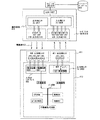
まず、図8(A)に示すように、IDラベルの基体となるラベル紙をラベル紙供給手段300(ロール1)から供給し、ラベル紙の所望の位置にIDFチップ(薄膜集積回路装置)を貼り付ける。この際、適宜、接着剤、ACFや、超音波接着法、UV接着法を用いる。ここでは、ラベル紙にアンテナが形成されているものとし、ACF供給手段301、IDFチップ貼付手段302によって、ACFを介してラベル紙とIDFチップとを接着した。勿論、ラベル紙に形成されたアンテナと、IDFチップは接続されている。次に、接着剤層供給手段303から、接着剤層を供給し、セパレート紙供給手段304(ロール2)から供給されるセパレート紙(セパレータ)を貼り付け、IDラベルが完成する。最後にラベル巻き取り手段305(ロール3)で、IDラベルを巻き取る。なお、IDラベル基体は、予め個々のラベル毎に分離しておき、セパレート紙は帯状のものを供給すると良い。この場合には、図34(A)に示すような、一連のラベル台紙118(セパレータ)上に、個々に分離されたIDラベル20を得ることができる。 First, as shown in FIG. 8A, a label paper serving as an ID label substrate is supplied from a label paper supply means 300 (roll 1), and an IDF chip (thin film integrated circuit device) is placed at a desired position on the label paper. paste. At this time, an adhesive, ACF, an ultrasonic bonding method, or a UV bonding method is appropriately used. Here, it is assumed that the antenna is formed on the label paper, and the label paper and the IDF chip are bonded by the ACF supply means 301 and the IDF chip attaching means 302 via the ACF. Of course, the antenna formed on the label paper and the IDF chip are connected. Next, the adhesive layer is supplied from the adhesive layer supply means 303, and the separate paper (separator) supplied from the separate paper supply means 304 (roll 2) is attached, thereby completing the ID label. Finally, the ID label is taken up by the label take-up means 305 (roll 3). The ID label substrate is preferably separated for each label in advance, and a separate paper sheet is preferably supplied. In this case, individually separated ID labels 20 can be obtained on a series of label mounts 118 (separators) as shown in FIG.
また、ラベル紙の供給と、セパレート紙の供給の順序は、図8(B)に示すように逆にしても良い。また、同図では、IDFチップにアンテナが一体形成されているものとし、ACF供給手段301は省略した。また、IDラベルが帯状に複数形成された後、型抜き機等のラベル分離手段306によってラベル分離を行い、個々のラベルの状態にしてから、製品として回収手段307によって回収しても良い。勿論、図8(A)と(B)は、交互に組み合わせることができる。
Further, the order of supply of label paper and supply of separate paper may be reversed as shown in FIG. In the figure, it is assumed that the antenna is integrally formed on the IDF chip, and the ACF supply means 301 is omitted. Alternatively, after a plurality of ID labels are formed in a strip shape, label separation may be performed by a label separation unit 306 such as a die cutting machine to obtain individual labels, and the product may be collected by the
なお、本実施形態に係る方法は、本発明に係るIDカード、IDタグ、紙幣、硬貨、証書類、無記名債券類、有価証券類等に、適宜採用することができる。例えば、IDタグの場合には、ロール1に下部基体材料を保持しておき、ロール2には、上部基体材料を保持しておけばよい。
The method according to the present embodiment can be appropriately employed for the ID card, ID tag, banknote, coin, certificate, bearer bond, securities, and the like according to the present invention. For example, in the case of an ID tag, the lower base material may be held on the
(実施形態8)
本発明に係るIDカードやIDタグの作製方法について、主に図9を参照して説明する。図9は、本発明に係るIDカード、IDタグの製造ラインを示した模式図及び完成品の拡大図を示したものである。
(Embodiment 8)
A method for manufacturing an ID card and an ID tag according to the present invention will be described mainly with reference to FIGS. FIG. 9 shows a schematic diagram showing a production line of an ID card and an ID tag according to the present invention and an enlarged view of a finished product.
まず、図9(A)に示すように、IDカード又はIDタグの基体となる材料を基体供給手段308(ロール1)から供給し、基体の所望の位置に、IDF貼付手段302によって、IDFチップ(薄膜集積回路装置)を貼り付ける。この際、適宜、接着剤、ACFや、超音波接着法、UV接着法を用いる。次に、基体が帯状に連なっているときは、基体分離手段309によって、基体を個々のIDカード又はIDタグ毎に分離する。そして、ラミネート装置310によって、個々の基体の周囲をラミネート加工する。これにより、IDカード又はIDタグが完成する。 First, as shown in FIG. 9A, a material for a base of an ID card or ID tag is supplied from a base supply means 308 (roll 1), and an IDF chip is placed at a desired position on the base by an IDF sticking means 302. (Thin film integrated circuit device) is attached. At this time, an adhesive, ACF, an ultrasonic bonding method, or a UV bonding method is appropriately used. Next, when the base is continuous in a strip shape, the base is separated into individual ID cards or ID tags by the base separating means 309. Then, the periphery of each substrate is laminated by the laminating apparatus 310. Thereby, the ID card or the ID tag is completed.
なお、帯状の基体の所望の位置にIDFチップを形成し、ラミネート加工を行った後に、個々のIDカード又はIDタグ毎に分離しても良い。ラミネート加工されたIDカード又はIDタグは、回収手段307によって回収される。 In addition, after forming an IDF chip | tip in the desired position of a strip | belt-shaped base | substrate and performing a lamination process, you may isolate | separate for every ID card or ID tag. The laminated ID card or ID tag is collected by the collecting means 307.
図9(B)は、本実施形態に係る方法を用いて作製されたIDカード又はIDタグの完成品の断面拡大図である。ラベル基体32には、アンテナ11と、該アンテナに接続された薄膜集積回路装置13が接続パット12を介して形成されており、保護層34、35を介して、フィルム層45に覆われている。なお、ラミネート加工時の加熱処理等において、薄膜集積回路装置やアンテナを保護するために、保護層34、35を形成しておくのが望ましい。保護層としては、DLC或いはCN等の炭素を有する膜、又は窒化珪素膜或いは窒化酸化珪素膜等を用いることができるが、これに限定されるものではない。形成方法としては、プラズマCVD法や、大気圧プラズマ等を用いることができる。
FIG. 9B is an enlarged cross-sectional view of a finished product of an ID card or ID tag manufactured using the method according to the present embodiment. The
かくして、ラミネート加工されたIDカード又はIDタグを得ることができる。なお、ラミネート加工に適した商品であれば、IDカード、IDタグに限らず、本製造プロセスを採用することができる。 Thus, a laminated ID card or ID tag can be obtained. Note that the manufacturing process is not limited to ID cards and ID tags as long as the product is suitable for laminating.
(実施形態9)
本発明に係るIDラベル、IDカードの構造及び作製方法について、主に図10〜12を参照して説明する。まず、図10は、本発明に係るIDラベルの積層構造を示した斜視図である。ここでは、商品等に貼り付けるラベル基体部分を上方に、ラベルの台紙となるセパレータを下方に示してある。
(Embodiment 9)
The structure and manufacturing method of the ID label and ID card according to the present invention will be described mainly with reference to FIGS. First, FIG. 10 is a perspective view showing a laminated structure of ID labels according to the present invention. Here, a label base portion to be attached to a product or the like is shown on the upper side, and a separator serving as a label mount is shown on the lower side.
図10は、IDラベル49において、アンテナ47と薄膜集積回路装置48とが一体形成されたアンテナ一体型薄膜集積回路装置46(以下、「アンテナ一体型IDFチップ」と呼ぶことがある。)を、接着剤層15を介してセパレータ16又はラベル基体10に貼り付ける方法を示したものである。なお、ラベル基体、接着剤層、セパレータの材質は、上記実施形態に準ずる。また、IDFチップ及びアンテナの形状は、図10の形状に限定されない。
FIG. 10 shows an antenna integrated thin film integrated circuit device 46 (hereinafter sometimes referred to as “antenna integrated IDF chip”) in which an antenna 47 and a thin film integrated
また、図11は、IDカード50において、アンテナ一体型薄膜集積回路装置46を、接着剤層15を介してカード下部基体37bに貼り付ける方法を示したものである。なお、カード下部基体、接着剤層の材質は、上記実施形態に準ずる。また、IDFチップ及びアンテナの形状は、図11の形状に限定されない。
FIG. 11 shows a method of attaching the antenna integrated thin film integrated
また、図12は、図11に示すIDラベル、IDカードにおけるアンテナ一体型IDFチップのX−Y方向の断面図を示したものである。 FIG. 12 is a cross-sectional view in the X-Y direction of the antenna-integrated IDF chip in the ID label and ID card shown in FIG.
図12(A)は、保護膜55上に、島状半導体膜57、ゲート絶縁膜58を形成した後に、ゲート電極56(ここでは、2層構造となっている)と交差配線52とを同時に形成する場合を示している。さらに、層間膜53を介して、アンテナ47、TFTとアンテナを接続するための配線51a、TFT同士を接続するための配線51bを形成した。ゲート電極56と交差配線52、及びアンテナ47と配線51a、51bは同一工程で作製するのが望ましいが、段階的に形成しても良い。 In FIG. 12A, after the island-shaped semiconductor film 57 and the gate insulating film 58 are formed over the protective film 55, the gate electrode 56 (in this case, has a two-layer structure) and the cross wiring 52 are simultaneously formed. The case where it forms is shown. Further, an antenna 47, a wiring 51a for connecting the TFT and the antenna, and a wiring 51b for connecting the TFTs are formed through the interlayer film 53. The gate electrode 56 and the cross wiring 52, and the antenna 47 and the wirings 51a and 51b are preferably formed in the same process, but may be formed in stages.
図12(B)は、保護膜55上に、島状半導体膜57、ゲート絶縁膜58を形成した後に、ゲート電極56(ここでは、2層構造となっている)とアンテナ47とを形成する場合を示している。さらに、層間膜53を介して、TFTとアンテナを接続するための配線51a、交差配線52、TFT同士を接続するための配線51bを形成した。ゲート電極56とアンテナ47、交差配線52と配線51a、51bは同一工程で作製するのが望ましいが、段階的に形成しても良い。 In FIG. 12B, after the island-shaped semiconductor film 57 and the gate insulating film 58 are formed over the protective film 55, the gate electrode 56 (in this case, has a two-layer structure) and the antenna 47 are formed. Shows the case. Further, a wiring 51 a for connecting the TFT and the antenna, a cross wiring 52, and a wiring 51 b for connecting the TFTs are formed via the interlayer film 53. The gate electrode 56 and the antenna 47, and the cross wiring 52 and the wirings 51a and 51b are preferably formed in the same process, but may be formed in stages.
なお、図12(A)(B)ともに、また、トップゲート構造のTFTを用いているが、勿論、ボトムゲート構造を採用しても良い。TFTの具体的な作製方法については、後述する。また、半導体層57への不純物拡散を防止するため、単層又は積層構造の保護膜55を形成しておくのが望ましい。また、アンテナを形成した後にも、保護膜54を形成しておくのが望ましい。なお、該保護層は、窒化珪素、酸化珪素、酸窒化珪素等を採用することができるが、Na等の不純物ブロッキング性を有する窒化珪素を含んでいることが望ましい。 In FIGS. 12A and 12B, a TFT having a top gate structure is used. Of course, a bottom gate structure may be adopted. A specific method for manufacturing the TFT will be described later. In order to prevent impurity diffusion into the semiconductor layer 57, it is desirable to form a protective film 55 having a single layer or a stacked structure. Further, it is desirable to form the protective film 54 after the antenna is formed. The protective layer may employ silicon nitride, silicon oxide, silicon oxynitride, or the like, but preferably includes silicon nitride having impurity blocking properties such as Na.
あるいは、層間膜や保護膜としては、弾性の高いポリイミド等の有機材料を用いてもよい。これにより、変形時の応力は、有機材料を有する層間膜や保護膜に集中し、主にこれらの膜が変形するので、薄膜トランジスタへかかる応力が低減される。また変形が生じる場合に、最も応力が負荷される箇所(エッジ、角)が、半導体膜のエッジではなく下地膜のエッジとなるため、半導体膜のエッジや界面で生じる応力集中を抑えることができる。 Alternatively, an organic material such as highly elastic polyimide may be used as the interlayer film and the protective film. Thereby, the stress at the time of deformation is concentrated on the interlayer film and the protective film having the organic material, and these films are mainly deformed, so that the stress applied to the thin film transistor is reduced. In addition, when deformation occurs, the most stressed portion (edge, corner) is not the edge of the semiconductor film but the edge of the base film, so that stress concentration occurring at the edge or interface of the semiconductor film can be suppressed. .
なお、IDFチップ110は、図25(A)に示すように、上下の保護層54a、55a、55bのほぼ中央部に配置せしめるのが望ましい。ここで、IDFチップは約5μm以下、好ましくは0.3〜3μmの厚さに形成され、一方、アンテナは一般的に5〜40μmの厚さ、保護膜は、上下それぞれ10〜200μmの厚さに形成される。したがって、上下保護膜、IDFチップ、アンテナ(アンテナが一体形成されている場合)の膜厚の総計をdとして、IDFチップを、x=(d/2)±30μmの位置、さらに好ましくは、x=(d/2)±10μmの位置に配置するのが望ましい(図25(B)、(C))。
As shown in FIG. 25A, it is desirable that the
このように、IDFチップを保護膜の中心に配置せしめることで、IDFチップへの応力を緩和することができ、TFTを構成する各層でのクラックの発生を防止することができる。 Thus, by placing the IDF chip in the center of the protective film, the stress on the IDF chip can be relaxed, and the occurrence of cracks in each layer constituting the TFT can be prevented.
以上は、TFTとアンテナを一体形成した場合の構造の一例であり、必ずしもこれらに限定されるものではない。 The above is an example of the structure when the TFT and the antenna are integrally formed, and the structure is not necessarily limited thereto.
本実施例では、図13〜16を参照して、薄膜集積回路装置の具体的な作製方法について説明する。ここでは、簡単のため、n型TFTとp型TFTを用いたCPUとメモリ部分の断面構造を示すことによって、その作製方法について説明する。 In this embodiment, a specific method for manufacturing a thin film integrated circuit device will be described with reference to FIGS. Here, for the sake of simplicity, a manufacturing method will be described by showing a cross-sectional structure of a CPU and a memory portion using n-type TFTs and p-type TFTs.
まず、基板60上に、剥離層61を形成する(図13(A))。ここでは、ガラス基板(例えば、コーニング社製1737基板)上に、50nm(500Å)の膜厚のa−Si膜(非晶質シリコン膜)をCVD法により形成した。なお、基板としては、ガラス基板の他にも、石英基板、アルミナなど絶縁物質で形成される基板、シリコンウエハ基板、後工程の処理温度に耐え得る耐熱性を有するプラスチック基板等を用いることができる。
First, the
また、剥離層としては、非晶質シリコンの他に、多結晶シリコン、単結晶シリコン、SAS(セミアモルファスシリコン(微結晶シリコンともいう。))等、シリコン(Si)を主成分とする層を用いることができる。これらの剥離層は、CVD法の他にも、スパッタ法等によって形成しても良い。また、剥離層は50nmよりも薄く形成しても良い。 In addition to the amorphous silicon, the separation layer includes a layer containing silicon (Si) as a main component, such as polycrystalline silicon, single crystal silicon, and SAS (semi-amorphous silicon (also referred to as microcrystalline silicon)). Can be used. These peeling layers may be formed by a sputtering method or the like in addition to the CVD method. Further, the peeling layer may be formed thinner than 50 nm.
次に、剥離層61上に、保護膜55(下地膜、下地絶縁膜と呼ぶこともある。)を形成する(図13(A))。ここでは、100nm(1000Å)の膜厚の窒化珪素膜をCVD法によって形成したが、材料、製法はこれに限定されるものではなく、酸化珪素膜、酸窒化珪素膜等を用いることもできる。また、単層でなく、積層構造とすることもできる。例えば、酸化窒化珪素膜(SiOxNy)(x>y)、窒化酸化珪素膜(SiNxOy)(x>y)(x、y=1、2・・・)、酸化窒化珪素膜の3層構造とするのがよい。 Next, a protective film 55 (also referred to as a base film or a base insulating film) is formed over the separation layer 61 (FIG. 13A). Here, a silicon nitride film having a thickness of 100 nm (1000 mm) is formed by a CVD method; however, the material and the manufacturing method are not limited thereto, and a silicon oxide film, a silicon oxynitride film, or the like can also be used. Further, not a single layer but also a laminated structure can be used. For example, a silicon oxynitride film (SiOxNy) (x> y), a silicon nitride oxide film (SiNxOy) (x> y) (x, y = 1, 2,...), And a silicon oxynitride film are used. It is good.
なお、剥離層61及び島状半導体膜57として、a−Si等の珪素を主成分とする材料を用いる場合には、それらに接する保護膜としては、密着性確保の点から、SiOxNyを用いるのが望ましい。
In addition, when using the material which has silicon as main components, such as a-Si, as the
次に、保護膜55上に、薄膜集積回路装置のCPUやメモリを構成する薄膜トランジスタ(TFT)を形成する。なお、TFT以外にも、有機TFT、薄膜ダイオード等の薄膜能動素子を形成することもできる。 Next, a thin film transistor (TFT) constituting a CPU and a memory of the thin film integrated circuit device is formed on the protective film 55. In addition to TFTs, thin film active elements such as organic TFTs and thin film diodes can also be formed.
TFTの作製方法として、まず、保護膜55上に、島状半導体膜57を形成する(図13(B))。島状半導体膜57は、アモルファス半導体、結晶性半導体、又はセミアモルファス半導体で形成する。いずれも、シリコン、シリコン・ゲルマニウム(SiGe)等を主成分とする半導体膜を用いることができる。 As a method for manufacturing a TFT, first, an island-shaped semiconductor film 57 is formed over the protective film 55 (FIG. 13B). The island-shaped semiconductor film 57 is formed using an amorphous semiconductor, a crystalline semiconductor, or a semi-amorphous semiconductor. In any case, a semiconductor film containing silicon, silicon germanium (SiGe), or the like as a main component can be used.
ここでは、70nmの膜厚のアモルファスシリコンを形成し、さらにその表面を、ニッケルを含む溶液で処理した後、500〜750℃の熱結晶化工程によって結晶質シリコン半導体膜を得、さらにレーザー結晶化を行って結晶性の改善を施した。また、成膜方法としては、プラズマCVD法、スパッタ法、LPCVD法などを用いても良いし、結晶化方法としては、レーザー結晶化法、熱結晶化法、他の触媒(Fe,Ru,Rh,Pd,Os,Ir,Pt,Cu,Au等)を用いた熱結晶化、あるいはそれらを交互に複数回行っても良い。 Here, after forming amorphous silicon with a film thickness of 70 nm and further treating the surface with a solution containing nickel, a crystalline silicon semiconductor film is obtained by a thermal crystallization process at 500 to 750 ° C., and further laser crystallization is performed. To improve the crystallinity. Further, as a film forming method, a plasma CVD method, a sputtering method, an LPCVD method, or the like may be used. As a crystallization method, a laser crystallization method, a thermal crystallization method, or another catalyst (Fe, Ru, Rh) is used. , Pd, Os, Ir, Pt, Cu, Au, etc.), or they may be alternately performed a plurality of times.
また、非晶質構造を有する半導体膜の結晶化処理としては、連続発振のレーザーを用いても良く、結晶化に際し大粒径の結晶を得るためには、連続発振が可能な固体レーザーを用い、基本波の第2高調波〜第4高調波を適用するのが好ましい(この場合の結晶化をCWLCという。)。代表的には、Nd:YVO4レーザー(基本波1064nm)の第2高調波(532nm)や第3高調波(355nm)を適用すればよい。連続発振のレーザーを用いる場合には、出力10Wの連続発振のYVO4レーザーから射出されたレーザー光を非線形光学素子により高調波に変換する。また、共振器の中にYVO4結晶又はGdVO4結晶と非線形光学素子を入れて、高調波を射出する方法もある。そして、好ましくは光学系により照射面にて矩形状または楕円形状のレーザー光に成形して、被処理体に照射する。このときのエネルギー密度は0.01〜100MW/cm2程度(好ましくは0.1〜10MW/cm2)が必要である。そして、10〜2000cm/s程度の速度でレーザー光に対して相対的に半導体膜を移動させて照射すればよい。 In addition, a continuous wave laser may be used for the crystallization treatment of the semiconductor film having an amorphous structure, and a solid laser capable of continuous oscillation is used in order to obtain a crystal having a large particle size upon crystallization. It is preferable to apply the second to fourth harmonics of the fundamental wave (the crystallization in this case is referred to as CWLC). Typically, a second harmonic (532 nm) or a third harmonic (355 nm) of an Nd: YVO 4 laser (fundamental wave 1064 nm) may be applied. In the case of using a continuous wave laser, laser light emitted from a continuous wave YVO 4 laser having an output of 10 W is converted into a harmonic by a non-linear optical element. There is also a method in which a YVO 4 crystal or GdVO 4 crystal and a non-linear optical element are placed in a resonator to emit harmonics. Preferably, the laser beam is shaped into a rectangular or elliptical shape on the irradiation surface by an optical system, and the object to be processed is irradiated. At this time, the energy density of approximately 0.01 to 100 MW / cm 2 (preferably 0.1 to 10 MW / cm 2) is required. Then, irradiation may be performed by moving the semiconductor film relative to the laser light at a speed of about 10 to 2000 cm / s.
また、パルス発振のレーザを用いる場合、通常、数十Hz〜数百Hzの周波数帯を用いるが、それよりも著しく高い10MHz以上の発振周波数を有するパルス発振レーザを用いてもよい(この場合の結晶化をMHzLCという。)。パルス発振でレーザ光を半導体膜に照射してから半導体膜が完全に固化するまでの時間は数十nsec〜数百nsecと言われているため、上記高周波数帯を用いることで、半導体膜がレーザ光によって溶融してから固化するまでに、次のパルスのレーザ光を照射できる。よって、従来のパルス発振のレーザを用いる場合と異なり、半導体膜
中において固液界面を連続的に移動させることができるので、走査方向に向かって連続的に成長した結晶粒を有する半導体膜が形成される。具体的には、含まれる結晶粒の走査方向における幅が10〜30μm、走査方向に対して垂直な方向における幅が1〜5μm程度の結晶粒の集合を形成することができる。該走査方向に沿って長く延びた単結晶の結晶粒を形成することで、少なくともTFTのチャネル方向には結晶粒界のほとんど存在しない半導体膜の形成が可能となる。
In the case of using a pulsed laser, a frequency band of several tens Hz to several hundreds Hz is usually used, but a pulsed laser having an oscillation frequency of 10 MHz or higher that is significantly higher than that may be used (in this case) Crystallization is referred to as MHzLC). It is said that the time from when the semiconductor film is irradiated with laser light by pulse oscillation until the semiconductor film is completely solidified is said to be several tens of nanoseconds to several hundreds of nanoseconds. The laser light of the next pulse can be irradiated after being melted by the laser light and solidifying. Therefore, unlike the case of using a conventional pulsed laser, the solid-liquid interface can be continuously moved in the semiconductor film, so that a semiconductor film having crystal grains continuously grown in the scanning direction is formed. Is done. Specifically, a set of crystal grains having a width of 10 to 30 μm in the scanning direction of the included crystal grains and a width of about 1 to 5 μm in a direction perpendicular to the scanning direction can be formed. By forming single crystal grains extending long along the scanning direction, it is possible to form a semiconductor film having almost no crystal grain boundaries in at least the channel direction of the TFT.
上記の方法によって結晶性シリコン半導体膜を得る。なお、結晶は、ソース、チャネル、ドレイン方向にそろっていることが望ましい。また、結晶層の厚さは、20〜200nm(代表的には40〜170nm、さらに好ましくは、50〜150nm)となるようにするのがよい。その後、半導体膜上に酸化膜を介して、金属触媒をゲッタリングするためのアモルファスシリコン膜を成膜し、500〜750℃の熱処理によってゲッタリング処理を行った。さらに、TFT素子としての閾値を制御するために、結晶性シリコン半導体膜に対し、1013/cm2オーダーのドーズ量のホウ素イオンを注入した。その後、レジストをマスクとしてエッチングを行うことにより、島状半導体膜57を形成した。 A crystalline silicon semiconductor film is obtained by the above method. Note that the crystals are preferably aligned in the source, channel, and drain directions. The thickness of the crystal layer is preferably 20 to 200 nm (typically 40 to 170 nm, more preferably 50 to 150 nm). Thereafter, an amorphous silicon film for gettering the metal catalyst was formed on the semiconductor film via an oxide film, and gettering treatment was performed by heat treatment at 500 to 750 ° C. Furthermore, in order to control the threshold value as the TFT element, boron ions having a dose of the order of 10 13 / cm 2 were implanted into the crystalline silicon semiconductor film. Thereafter, the island-shaped semiconductor film 57 was formed by etching using the resist as a mask.
なお、結晶性半導体膜を形成するにあたっては、ジシラン(Si2H6)とフッ化ゲルマニウム(GeF4)の原料ガスとして、LPCVD法によって、多結晶半導体膜を直接形成することによっても、結晶性半導体膜を得ることができる。ガス流量比は、Si2H6/GeF4=20/0.9、成膜温度は400〜500℃、キャリアガスとしてHe又はArを用いたが、これに限定されるものではない。 Note that in forming the crystalline semiconductor film, the crystalline semiconductor film can also be formed by directly forming a polycrystalline semiconductor film by LPCVD as a source gas of disilane (Si 2 H 6 ) and germanium fluoride (GeF 4 ). A semiconductor film can be obtained. The gas flow ratio is Si 2 H 6 / GeF 4 = 20 / 0.9, the film forming temperature is 400 to 500 ° C., and He or Ar is used as the carrier gas, but the present invention is not limited to this.
なお、TFT内の特にチャネル領域には、5×10¹⁵〜2.5×1021cm-3(0.00001〜5原子%)、好ましくは、0.0005〜5原子%の水素又はハロゲンが添加されているのがよい。いずれにしても、ICチップに用いられる単結晶に含まれる水素又はハロゲンの含有量よりも多く含有させておくことが望ましい。これにより、TFT部に局部クラックが生じても、水素又はハロゲンによってターミネート(終端)されうる。 Note that in the channel region in the TFT in particular, 5 × 10 15 to 2.5 × 10 21 cm −3 (0.00001 to 5 atomic%), preferably 0.0005 to 5 atomic% of hydrogen or halogen is contained. It should be added. In any case, it is desirable to contain more than the content of hydrogen or halogen contained in the single crystal used for the IC chip. Thereby, even if a local crack occurs in the TFT portion, it can be terminated (terminated) by hydrogen or halogen.
次に、島状半導体膜57上にゲート絶縁膜58を形成する(図13(B))。ゲート絶縁膜はプラズマCVD法又はスパッタリング法などの薄膜形成法を用い、窒化珪素、酸化珪素、窒化酸化珪素又は酸化窒化珪素を含む膜を、単層で、又は積層させて形成することが好ましい。積層する場合には、例えば、基板側から酸化珪素膜、窒化珪素膜、酸化珪素膜の3層構造とするのがよい。 Next, a gate insulating film 58 is formed over the island-shaped semiconductor film 57 (FIG. 13B). The gate insulating film is preferably formed using a thin film formation method such as a plasma CVD method or a sputtering method, and a film containing silicon nitride, silicon oxide, silicon nitride oxide, or silicon oxynitride is formed as a single layer or a stacked layer. In the case of stacking, for example, a three-layer structure of a silicon oxide film, a silicon nitride film, and a silicon oxide film is preferable from the substrate side.
次に、ゲート電極56を形成する(図13(C))。ここでは、30nmの膜厚のTaN(窒化タンタル)と、370nmの膜厚のW(タングステン)をスパッタ法により積層形成した後に、レジスト62をマスクとしてエッチングを行うことにより、ゲート電極56を形成した。ここで、レジストマスクの代わりに、SiOx等のマスクを用いてもよい。この場合、SiOx、SiON等のマスク(ハードマスクと呼ばれる。)をパターニング形成工程が加わるが、エッチング時におけるマスクの膜減りがレジストよりも少ないため、所望の幅のゲート電極層を形成することができる。勿論、ゲート電極56の材料、構造、作製方法は、これに限定されるものではなく、適宜選択することができる。例えば、レジスト62を用いずに、液滴吐出法を用いて選択的にゲート電極56を形成しても良い。 Next, the gate electrode 56 is formed (FIG. 13C). In this case, TaN (tantalum nitride) with a thickness of 30 nm and W (tungsten) with a thickness of 370 nm are stacked by sputtering, and then etched using the resist 62 as a mask to form the gate electrode 56. . Here, a mask made of SiOx or the like may be used instead of the resist mask. In this case, a patterning process is added to a mask (referred to as a hard mask) made of SiOx, SiON, or the like. However, since the film thickness of the mask during etching is less than that of the resist, a gate electrode layer having a desired width may be formed. it can. Of course, the material, structure, and manufacturing method of the gate electrode 56 are not limited to this, and can be selected as appropriate. For example, the gate electrode 56 may be selectively formed using a droplet discharge method without using the resist 62.
なお、導電材料としては、導電膜の機能に応じて種々の材料を選択することができるが、代表的なものとして、銀(Ag)、銅(Cu)、金(Au)、ニッケル(Ni)、白金(Pt)、クロム(Cr)、スズ(Sn)、パラジウム(Pd)、イリジウム(Ir)、ロジウム(Rh)、ルテニウム(Ru)、レニウム(Re)、タングステン(W)、アルミニウム(Al)、タンタル(Ta)、インジウム(In)、テルル(Te)、モリブデン(Mo)、カドミウム(Cd、亜鉛(Zn)、鉄(Fe)、チタン(Ti)、シリコン(Si)、ゲルマニウム(Ge)、ジルコニウム(Zr)、バリウム(Ba)、アンチモン鉛、酸化スズ・アンチモン、フッ素ドープ酸化亜鉛、炭素、グラファイト、グラッシーカーボン、リチウム、ベリリウム、ナトリウム、マグネシウム、カリウム、カルシウム、スカンジウム、マンガン、ジルコニウム、ガリウム、ニオブ、ナトリウム−カリウム合金、マグネシウム/銅混合物、マグネシウム/銀混合物、マグネシウム/アルミニウム混合物、マグネシウム/インジウム混合物、アルミニウム/酸化アルミニウム混合物、リチウム/アルミニウム混合物等、ハロゲン化銀の微粒子等、又は分散性ナノ粒子、あるいは、透明導電膜として用いられるITO:Indium Tin Oxide、ITSO、ZnO、GZO、IZO、有機インジウム、有機スズ、窒化チタン等を適宜採用することができる。 Note that various materials can be selected as the conductive material depending on the function of the conductive film, but typical ones are silver (Ag), copper (Cu), gold (Au), nickel (Ni). , Platinum (Pt), chromium (Cr), tin (Sn), palladium (Pd), iridium (Ir), rhodium (Rh), ruthenium (Ru), rhenium (Re), tungsten (W), aluminum (Al) Tantalum (Ta), indium (In), tellurium (Te), molybdenum (Mo), cadmium (Cd, zinc (Zn), iron (Fe), titanium (Ti), silicon (Si), germanium (Ge), Zirconium (Zr), barium (Ba), antimony lead, tin oxide / antimony, fluorine-doped zinc oxide, carbon, graphite, glassy carbon, lithium, beryllium Sodium, magnesium, potassium, calcium, scandium, manganese, zirconium, gallium, niobium, sodium-potassium alloy, magnesium / copper mixture, magnesium / silver mixture, magnesium / aluminum mixture, magnesium / indium mixture, aluminum / aluminum oxide mixture, ITO / Indium Tin Oxide, ITSO, ZnO, GZO, IZO, organic indium, organic tin, titanium nitride, etc. used as a lithium / aluminum mixture, silver halide fine particles, or the like, or dispersible nanoparticles, or a transparent conductive film Can be adopted as appropriate.
なお、ゲート電極をエッチング形成する際のエッチングガスとしては、CF4、Cl2、O2の混合ガスやCl2ガスを用いたが、これに限定されるものではない。 Note that although a mixed gas of CF 4 , Cl 2 , and O 2 or Cl 2 gas is used as an etching gas for forming the gate electrode by etching, it is not limited to this.
次に、p型TFT70、72となる部分をレジスト63で覆い、ゲート電極をマスクとして、n型TFT69、71の島状半導体膜中に、n型を付与する不純物元素64(代表的にはP(リン)又はAs(砒素))を低濃度にドープする(第1のドーピング工程、図13(D))。第1のドーピング工程の条件は、ドーズ量:1×10¹³〜6×10¹³/cm2、加速電圧:50〜70keVとしたが、これに限定されるものではない。この第1のドーピング工程によって、ゲート絶縁膜58を介してスルードープがなされ、一対の低濃度不純物領域65が形成される。なお、第1のドーピング工程は、p型TFT領域をレジストで覆わずに、全面に行っても良い。
Next, the portions to become the p-type TFTs 70 and 72 are covered with a resist 63, and the gate electrode is used as a mask, and the impurity element 64 (typically P-type) imparting n-type is formed in the island-shaped semiconductor films of the n-type TFTs 69 and 71. (Phosphorus) or As (arsenic)) is doped at a low concentration (first doping step, FIG. 13D). The conditions of the first doping step are a dose of 1 × 10 13 to 6 × 10 13 / cm 2 and an acceleration voltage of 50 to 70 keV, but are not limited thereto. Through the first doping process, through doping is performed through the gate insulating film 58, and a pair of low-
次に、レジスト63をアッシング等により除去した後、n型TFT領域を覆うレジスト66を新たに形成し、ゲート電極をマスクとして、p型TFT70、72の島状半導体膜中に、p型を付与する不純物元素67(代表的にはB(ホウ素))を高濃度にドープする(第2のドーピング工程、図13(E))。第2のドーピング工程の条件は、ドーズ量:1×10¹⁶〜3×10¹⁶/cm2、加速電圧:20〜40keVとして行う。この第2のドーピング工程によって、ゲート絶縁膜58を介してスルードープがなされ、一対のp型の高濃度不純物領域68が形成される。
Next, after removing the resist 63 by ashing or the like, a resist 66 covering the n-type TFT region is newly formed, and p-type is imparted to the island-like semiconductor films of the p-type TFTs 70 and 72 using the gate electrode as a mask. The
次に、レジスト66をアッシング等により除去した後、基板表面に、絶縁膜75を形成した(図14(A))。ここでは、膜厚100nmのSiON(酸窒化珪素)膜と、膜厚200nmのLTO膜(Low Temperature Oxide、低温酸化膜)の2層構造とした。ここでは、SiON膜は、プラズマCVD法で形成し、LTO膜としは、SiO2膜を減圧CVD法で形成した。その後、図示しないが、基板のTFTが形成された側をレジストで覆い、基板の裏面に形成された絶縁膜をエッチング除去した(裏面処理)。 Next, after removing the resist 66 by ashing or the like, an insulating film 75 was formed on the substrate surface (FIG. 14A). Here, a two-layer structure of a SiON (silicon oxynitride) film having a thickness of 100 nm and an LTO film (Low Temperature Oxide, low temperature oxide film) having a thickness of 200 nm is employed. Here, the SiON film was formed by the plasma CVD method, and the SiO 2 film was formed by the low pressure CVD method as the LTO film. Thereafter, although not shown, the side of the substrate on which the TFT was formed was covered with a resist, and the insulating film formed on the back surface of the substrate was removed by etching (back surface treatment).
次に、基板のTFT側に形成されたレジストを残したまま、エッチバック法により、レジスト及び絶縁膜75をエッチング除去し、サイドウォール(側壁)76を自己整合的(セルフアライン)に形成した(図14(B))。エッチングガスとしては、CHF3とHeの混合ガスを用いた。なお、サイドウォールを形成する工程は、これらに限定されるものではない。 Next, while leaving the resist formed on the TFT side of the substrate, the resist and the insulating film 75 are removed by etching using an etch-back method, and sidewalls (side walls) 76 are formed in a self-aligned manner (self-alignment) ( FIG. 14B). As the etching gas, a mixed gas of CHF 3 and He was used. Note that the step of forming the sidewall is not limited to these.
次に、p型TFT領域を覆うレジスト77を新たに形成し、ゲート電極56及びサイドウォール76をマスクとして、n型を付与する不純物元素78(代表的にはP又はAs)を高濃度にドープする(第3のドーピング工程、図14(C))。第3のドーピング工程の条件は、ドーズ量:1×10¹³〜5×10¹⁵/cm2、加速電圧:60〜100keVとして行う。この第3のドーピング工程によって、ゲート絶縁膜58を介してスルードープがなされ、一対のn型の高濃度不純物領域79が形成される。
Next, a resist 77 covering the p-type TFT region is newly formed, and an n-type impurity element 78 (typically P or As) is doped at a high concentration using the gate electrode 56 and the sidewall 76 as a mask. (Third doping step, FIG. 14C). The conditions of the third doping step are a dose amount: 1 × 10 13 to 5 × 10 15 / cm 2 and an acceleration voltage: 60 to 100 keV. Through the third doping step, through doping is performed through the gate insulating film 58, and a pair of n-type high
なお、図示しないが、レジスト77をアッシング等により除去した後、不純物領域の熱活性化を行っても良い。例えば、50nmのSiON膜を成膜した後、550℃、4時間、窒素雰囲気下において、加熱処理を行えばよい。また、水素を含むSiNx膜を、100nmの膜厚に形成した後、410℃、1時間、窒素雰囲気下において、加熱処理を行うことにより、結晶性半導体膜の欠陥を改善することができる。これは、例えば、結晶性シリコン中に存在するダングリングボンドを終端させるものであり、水素化処理工程などと呼ばれる。さらに、この後、TFTを保護するキャップ絶縁膜として、膜厚600nmのSiON膜を形成する。なお、水素化処理工程は、該SiON膜形成後に行っても良い。この場合、SiNx、SiON膜は連続成膜することができる。このように、TFT上には、SiON、SiNx、SiONの3層の絶縁膜が形成されることになるが、その構造や材料はこれらに限定されるものではない。また、これらの絶縁膜は、TFTを保護する機能をも有しているため、できるだけ形成しておくのが望ましい。 Although not shown, the impurity regions may be thermally activated after the resist 77 is removed by ashing or the like. For example, after a 50 nm SiON film is formed, heat treatment may be performed in a nitrogen atmosphere at 550 ° C. for 4 hours. In addition, after the SiNx film containing hydrogen is formed to a thickness of 100 nm, defects in the crystalline semiconductor film can be improved by performing heat treatment at 410 ° C. for 1 hour in a nitrogen atmosphere. This terminates dangling bonds existing in, for example, crystalline silicon, and is called a hydrogenation process. Thereafter, a SiON film having a film thickness of 600 nm is formed as a cap insulating film for protecting the TFT. Note that the hydrogenation process may be performed after the formation of the SiON film. In this case, the SiNx and SiON films can be continuously formed. Thus, a three-layer insulating film of SiON, SiNx, and SiON is formed on the TFT, but the structure and material are not limited to these. In addition, these insulating films have a function of protecting the TFT, so that it is desirable to form them as much as possible.
次に、TFT上に、層間膜53を形成する(図14(D))。層間膜53としては、ポリイミド、アクリル、ポリアミドや、シロキサン等の耐熱性有機樹脂を用いることができる。形成方法としては、その材料に応じて、スピンコート、ディップ、スプレー塗布、液滴吐出法、ドクターナイフ、ロールコーター、カーテンコーター、ナイフコーター等を採用することができる。また、無機材料を用いてもよく、その際には、PSG、BPSG、アルミナ膜等を用いることができる。なお、これらの絶縁膜を積層させて、層間膜53を形成しても良い。 Next, an interlayer film 53 is formed over the TFT (FIG. 14D). As the interlayer film 53, a heat-resistant organic resin such as polyimide, acrylic, polyamide, or siloxane can be used. As a forming method, a spin coat, dip, spray coating, droplet discharge method, doctor knife, roll coater, curtain coater, knife coater, or the like can be employed depending on the material. In addition, an inorganic material may be used, and in that case, PSG, BPSG, an alumina film, or the like can be used. Note that the interlayer film 53 may be formed by stacking these insulating films.
次に、レジストを形成した後、エッチングによりコンタクトホールを開孔し、TFT同士を接続する配線51及び外部アンテナと接続するための接続配線21を形成する(図14(D))。コンタクトホール開孔時のエッチングに用いられるガスは、CHF3とHeの混合ガスを用いたが、これに限定されるものではない。また、配線51と接続配線21は同一材料を用いて同時に形成しても良いし、別々に形成しても良い。ここでは、TFTと接続される配線51は、Ti、TiN、Al−Si、Ti及びTiNの5層構造とし、スパッタ法によって形成した後、パターニング形成した。
Next, after forming a resist, a contact hole is formed by etching, and a wiring 51 for connecting TFTs and a
なお、Al層において、Siを混入させることにより、配線パターニング時のレジストベークにおけるヒロックの発生を防止することができる。また、Siの代わりに、0.5%程度のCuを混入させても良い。また、TiやTiNでAl−Si層をサンドイッチすることにより、耐ヒロック性がさらに向上する。なお、パターニング時には、SiON等からなる上記ハードマスクを用いるのが望ましい。なお、配線の材料や、形成方法はこれらに限定されるものではなく、前述したゲート電極に用いられる材料を採用しても良い。 In addition, by mixing Si in the Al layer, generation of hillocks in resist baking during wiring patterning can be prevented. Further, instead of Si, about 0.5% Cu may be mixed. Further, the hillock resistance is further improved by sandwiching the Al—Si layer with Ti or TiN. In the patterning, it is desirable to use the hard mask made of SiON or the like. Note that the wiring material and the formation method are not limited to these, and the material used for the gate electrode described above may be employed.
なお、上記保護膜としては、DLC或いはCN等の炭素を有する膜、又は窒化珪素膜或いは窒化酸化珪素膜等を用いることができる。形成方法としては、プラズマCVD法や、大気圧プラズマ等を用いることができる。 Note that as the protective film, a film containing carbon such as DLC or CN, a silicon nitride film, a silicon nitride oxide film, or the like can be used. As a formation method, a plasma CVD method, an atmospheric pressure plasma, or the like can be used.
あるいは、ポリイミド、アクリル、ポリアミド、レジスト又はベンゾシクロブテン等の感光性又は非感光性の有機材料や、シロキサン等の耐熱性有機樹脂、を用いることができる。形成方法としては、その材料に応じて、スピンコート、ディップ、スプレー塗布、液滴吐出法、ドクターナイフ、ロールコーター、カーテンコーター、ナイフコーター等を採用することができる。あるいは、塗布法により得られるSOG膜(例えば、アルキル基を含むSiOx膜)を用いることもできる。また、無機材料を用いてもよく、その際には、酸化珪素、窒化珪素、酸窒化珪素、PSG、BPSG、アルミナ膜等を用いることができる。なお、これらの絶縁膜を積層させて、上記保護膜を形成しても良い。 Alternatively, a photosensitive or non-photosensitive organic material such as polyimide, acrylic, polyamide, resist, or benzocyclobutene, or a heat-resistant organic resin such as siloxane can be used. As a forming method, a spin coat, dip, spray coating, droplet discharge method, doctor knife, roll coater, curtain coater, knife coater, or the like can be employed depending on the material. Alternatively, an SOG film obtained by a coating method (for example, an SiOx film containing an alkyl group) can also be used. In addition, an inorganic material may be used. In that case, silicon oxide, silicon nitride, silicon oxynitride, PSG, BPSG, an alumina film, or the like can be used. Note that the protective film may be formed by stacking these insulating films.
なお、本実施例では、CPU73、メモリ74等を構成するTFT領域とアンテナと接続する端子部80のみを一体形成する場合について示したが、TFT領域とアンテナとを一体形成する場合にも、本実施例を適用できる。この場合には、層間膜53又は保護膜54上にアンテナを形成し、さらに、別の保護膜で覆うと良い。 In the present embodiment, the case where only the TFT region constituting the CPU 73, the memory 74, etc. and the terminal portion 80 connected to the antenna are integrally formed has been shown. Embodiments can be applied. In this case, an antenna is preferably formed on the interlayer film 53 or the protective film 54 and further covered with another protective film.
アンテナの導電材料としては、Ag、Au、Al、Cu、Zn、Sn、Ni、Cr、Fe、Co若しくはTi、又はそれらを含む合金を用いることができるが、これらに限定されるものではない。また、配線とアンテナで材料が異なっていても良い。なお、配線及びアンテナは、展性、延性に富む金属材料を有するように形成し、更に好ましくは膜厚を厚くして変形による応力に耐えるようにするのが望ましい。 As the conductive material of the antenna, Ag, Au, Al, Cu, Zn, Sn, Ni, Cr, Fe, Co, or Ti, or an alloy containing them can be used, but is not limited thereto. Further, the material may be different between the wiring and the antenna. Note that the wiring and the antenna are preferably formed so as to have a metal material having excellent malleability and ductility, and more preferably, the wiring and the antenna are made thick to withstand stress due to deformation.
また、形成方法としては、スパッタ法によって全面成膜した後、レジストマスクを用いてパターニングを行ってもよいし、液滴吐出法によってノズルから選択的に形成しても良い。なお、ここでいう液滴吐出法には、インクジェット法のみならず、オフセット印刷法やスクリーン印刷等も含まれる。配線とアンテナは、同時に形成しても良いし、一方を先に形成した後に、他方が乗り上げるように形成しても良い。 As a formation method, after forming a film on the entire surface by a sputtering method, patterning may be performed using a resist mask, or selective formation from a nozzle may be performed by a droplet discharge method. Note that the droplet discharge method here includes not only an inkjet method but also an offset printing method and a screen printing. The wiring and the antenna may be formed at the same time, or may be formed so that the other rides on after forming one first.
また、薄膜集積回路装置を内蔵する商品が、導電材料を含む場合には、それと同様の導電材料を用いて、アンテナ又は配線を形成しても良い。例えば、硬貨の材料を用いて硬貨の内部にアンテナを形成することができる。この場合、例えば、10円玉に薄膜集積回路装置を埋め込む場合には、銅、亜鉛、スズの合金からなるアンテナを形成すると良い。 In the case where a product incorporating a thin film integrated circuit device contains a conductive material, an antenna or a wiring may be formed using the same conductive material. For example, an antenna can be formed inside a coin using a coin material. In this case, for example, when a thin film integrated circuit device is embedded in a 10-yen coin, an antenna made of an alloy of copper, zinc, and tin is preferably formed.
なお、本実施例では、トップゲート構造としたが、ボトムゲート構造(逆スタガ構造)としてもよい。なお、TFTのような薄膜能動素子部(アクティブエレメント)の存在しない領域には、下地絶縁膜材料、層間絶縁膜材料、配線材料が主として設けられているが、該領域は、薄膜集積回路装置全体の50%以上、好ましくは60〜95%を占めていることが望ましい。これにより、IDFチップを曲げやすくし、IDラベル等の完成品の取り扱いが容易となる。この場合、TFT部を含むアクティブエレメントの島状半導体領域(アイランド)は、薄膜集積回路装置全体の5〜50%、好ましくは、5〜15%を占めているのがよい。 Although the top gate structure is used in this embodiment, a bottom gate structure (reverse stagger structure) may be used. Note that a base insulating film material, an interlayer insulating film material, and a wiring material are mainly provided in a region where a thin film active element portion (active element) such as a TFT does not exist, and this region is the entire thin film integrated circuit device. It is desirable to occupy 50% or more, preferably 60 to 95%. This makes it easy to bend the IDF chip and facilitates handling of finished products such as ID labels. In this case, the island-shaped semiconductor region (island) of the active element including the TFT portion occupies 5 to 50%, preferably 5 to 15% of the entire thin film integrated circuit device.
また、本実施例で作製したTFTのS値(サブスレッシュホールド値)は、0.35V/dec以下(好ましくは、0.07〜0.25V/dec)、移動度は、10cm2V/sec以上を有している。また、リングオシレータレベルで、1MHz以上、好ましくは10MHz以上の特性(3〜5Vにおいて)を有している、又は、ゲートあたりの周波数特性を100kHz以上、好ましくは1MHz以上(3〜5Vにおいて)有している。 Further, the S value (subthreshold value) of the TFT manufactured in this example is 0.35 V / dec or less (preferably 0.07 to 0.25 V / dec), and the mobility is 10 cm 2 V / sec. It has the above. Also, at the ring oscillator level, it has a characteristic of 1 MHz or more, preferably 10 MHz or more (at 3 to 5 V), or a frequency characteristic per gate of 100 kHz or more, preferably 1 MHz or more (at 3 to 5 V). is doing.
基板60上に、複数のTFT、保護膜、各種配線、アンテナ一体型の場合にはアンテナ(これらを総称して、「薄膜集積回路装置13」という。)を形成したら(図15(A))、次に、薄膜集積回路装置13の境界領域に、ダイシングによって溝81を形成する(図15(B))。この際、ダイシング装置(ダイサー;dicer)を用いるブレードダイシング法を用いるのが一般的である。ブレード(blade)とは、ダイヤモンド砥粒を埋め込んだ砥石で、その幅は約30〜50μmであり、このブレードを高速回転させることにより、薄膜集積回路を分離する。また、ダイシングに必要なエリアをストリートと呼ぶが、この幅は、素子への損傷を考慮し、80〜150μmとしておくのが望ましい。
When a plurality of TFTs, protective films, various wirings, and an antenna integrated type are formed on the
なお、ダイシングの他にも、スクライビング又はマスクを利用したエッチング等によって行うことができる。スクライビングの場合には、ダイヤモンドスクライビング法とレーザースクライビング法等がある。レーザースクライビング法を採用する場合には、レーザー共振器から、パルス発振のパワーが200〜300Wの線状レーザー、例えばNd:YAGレーザーであって、発振波長1064nmの基本波又は発振波長532nmの第2高調波等を用いることができる。 In addition to dicing, scribing or etching using a mask can be used. In the case of scribing, there are a diamond scribing method and a laser scribing method. When the laser scribing method is employed, a linear laser having a pulse oscillation power of 200 to 300 W, for example, an Nd: YAG laser, from a laser resonator, a fundamental wave having an oscillation wavelength of 1064 nm or a second laser having an oscillation wavelength of 532 nm is used. Harmonics and the like can be used.
また、エッチングの場合には、露光、現像工程によりマスクパターンを形成し、ドライエッチング、ウエットエッチング等により素子分離を行うことができる。ドライエッチングにおいては、大気圧プラズマ法を用いてもよい。 In the case of etching, a mask pattern can be formed by exposure and development processes, and element isolation can be performed by dry etching, wet etching, or the like. In dry etching, an atmospheric pressure plasma method may be used.
なお、溝を形成する場合、溝の深さは、少なくとも剥離層の表面が露出する程度とすればよく、基板60が繰り返し利用できるように、基板に傷が付かないように上記ダイシング等を適宜制御するのが望ましい。
When forming the groove, the depth of the groove may be at least enough to expose the surface of the release layer, and the above dicing or the like is appropriately performed so that the
次に、突起部82を有するジグ(支持基板)83を、接着剤84を介して、薄膜集積回路装置13毎に取り付ける(図15(C))。ここで、ジグ(治具)とは、剥離層を除去した後に薄膜集積回路がバラバラに分離しないように、一時的に薄膜集積回路を固定する役割を有する。ジグの形状としては、図15(C)のように、後にハロゲン化フッ素を含む気体又は液体の導入を容易にするために、突起部を設けた櫛状の構造とするのが望ましいが、平坦なジグを用いても構わない。また、さらに好ましくは、後にハロゲン化フッ素を含む気体又は液体の導入を容易にするための、開口部85を設けておいても良い。
Next, a jig (support substrate) 83 having a protrusion 82 is attached to each thin film integrated
ジグとしては、ハロゲン化フッ素によって冒されない酸化珪素を主成分とするガラス基板、石英基板、ステンレス(SUS)基板等を用いることができるが、ハロゲン化フッ素によって冒されない材料であれば、これらに限定されるものではない。 As the jig, a glass substrate mainly composed of silicon oxide not affected by fluorine halide, a quartz substrate, a stainless steel (SUS) substrate, or the like can be used. However, the material is not limited as long as the material is not affected by fluorine halide. Is not to be done.
ここで、接着剤としては、UV光照射によって接着力(粘着力)が低下又は喪失する材料を用いることができる。ここでは、日東電工社製UV照射剥離テープを用いた。これ以外にも、上述した再剥離再接着可能な接着剤を用いても構わない。例えば、特開2001−30403、特許2992092、特開平6−299127に記載された、アクリル系粘着剤、合成ゴム系粘着剤、天然ゴム系粘着剤等を用いることができる。勿論、ジグを簡単に取り外すことができる材料であれば、これらに限定されるものではない。 Here, as the adhesive, a material whose adhesive strength (adhesive strength) is reduced or lost by UV light irradiation can be used. Here, a UV irradiation peeling tape manufactured by Nitto Denko Corporation was used. In addition to this, the above-described re-peelable and re-adhesive adhesive may be used. For example, an acrylic pressure-sensitive adhesive, a synthetic rubber pressure-sensitive adhesive, a natural rubber pressure-sensitive adhesive and the like described in JP-A-2001-30403, JP-A-2992092, and JP-A-6-299127 can be used. Of course, the material is not limited to these as long as the jig can be easily removed.
次に、溝81にハロゲン化フッ素ガスを導入することにより、剥離層であるa−Si膜をエッチング除去した(図16(A))。ここでは、図21に示すような減圧CVD装置を用い、ガス:ClF3(三フッ化塩素)、温度:350℃、流量:300sccm、気圧:6Torr、時間:3時間の条件で行ったが、この条件に限定されるものではない。また、ClF3ガスに窒素を混ぜたガスを用いてもよい。両者の流量比は適宜設定することができる。なお、ClF3以外にも、BrF3、ClF2等のガスを用いてもよい。 Next, a halogenated fluorine gas was introduced into the groove 81 to remove the a-Si film as a peeling layer by etching (FIG. 16A). Here, a low pressure CVD apparatus as shown in FIG. 21 was used, and the conditions were as follows: gas: ClF 3 (chlorine trifluoride), temperature: 350 ° C., flow rate: 300 sccm, atmospheric pressure: 6 Torr, time: 3 hours. It is not limited to this condition. Alternatively, a gas in which nitrogen is mixed with ClF 3 gas may be used. The flow ratio between the two can be set as appropriate. In addition to ClF 3 , a gas such as BrF 3 or ClF 2 may be used.
ここで、図21に示す減圧CVD装置は、反応空間であるベルジャー100内に、ClF3ガス86等のハロゲン化フッ素ガスが導入され、ガスが基板101に行き渡る仕組みになっている。ベルジャーの外部にはヒーター102が設けられている。また、残余ガスは、排気管103から排出される。 Here, the low-pressure CVD apparatus shown in FIG. 21 has a mechanism in which a halogenated fluorine gas such as ClF 3 gas 86 is introduced into the bell jar 100 which is a reaction space, and the gas spreads over the substrate 101. A heater 102 is provided outside the bell jar. Further, the residual gas is discharged from the exhaust pipe 103.
ここで、ClF3等のハロゲン化フッ素は、珪素を選択的にエッチングするという特性がある反面、酸化珪素(SiOx)、窒化珪素(SiNx)、酸窒化珪素はほとんどエッチングされない。したがって、時間の経過ととも剥離層61はエッチングされ、最終的に基板60を剥離することができる(図16(B))。一方、酸化珪素、窒化珪素、酸窒化珪素等や、耐熱性樹脂からなる下地膜である保護膜や、層間膜、保護膜はほとんどエッチングされないため、薄膜集積回路への損傷を防止することができる。なお、剥離した基板60は勿論再利用することができ、コスト削減に繋がる。
Here, fluorine halide such as ClF 3 has a characteristic of selectively etching silicon, but silicon oxide (SiOx), silicon nitride (SiNx), and silicon oxynitride are hardly etched. Therefore, the
なお、剥離層61としては、ClF3等のハロゲン化フッ素によって除去可能なものであれば、上記シリコン系材料に限定されるものではない。また、保護膜や層間膜も、ClF3等のハロゲン化フッ素によって冒されないものであれば、上記材料に限定されない。
The
次に、UV光照射を行うことにより、接着剤84の粘着力を低下又は喪失させ、ジグと、薄膜集積回路装置とを分離することにより、大量に薄膜集積回路装置13を得ることができる。なお、ジグは、コスト削減のため、再利用するのが望ましい。
Next, the adhesive strength of the adhesive 84 is reduced or lost by performing UV light irradiation, and the jig and the thin film integrated circuit device are separated, whereby a large amount of the thin film integrated
上記方法によって作製された薄膜集積回路装置13は、図2に示すような小型真空ピンセット24や、微少サイズのピン等により搬送し、IDラベル、IDカード等の物品の所望の位置に備え付けることができる。
The thin film integrated
また、基板を剥離する方法として、複数の薄膜集積回路が形成された基板にストレスを与え、基板を物理的に剥離する方法を採用しても良い。この場合には、剥離層として、W、SiO2、WO3等を用いることができる。ストレスを与えるには、ダイヤモンドペン等で衝撃を与えればよい。 Further, as a method for peeling the substrate, a method in which stress is applied to the substrate on which a plurality of thin film integrated circuits are formed and the substrate is physically peeled may be employed. In this case, W, SiO 2 , WO 3 or the like can be used as the release layer. In order to give stress, a shock may be given with a diamond pen or the like.
本実施例では、図15(B)における溝81を形成するにあたり、ドライエッチング法を用いる場合について、図17を用いて説明する。図17(A)において、図15(A)の状態までは、実施例1と同様である。その後、現像、露光工程を経て、基板上にレジスト87を形成し、レジスト87をマスクとして、ドライエッチングにより溝81を形成し、素子分離を行う(図17(A))。ここでは、プラズマエッチングを採用し、エッチング用ガスとしては、Cl2、BCl3、SiCl4もしくはCCl4などを代表とする塩素系ガス、CF4、SF6、NF3、CHF3などを代表とするフッ素系ガス、あるいはO2を用いたが、これらに限定されるものではない。なお、該エッチングは、大気圧プラズマを利用して行うこともできる。この際、エッチングガスとしては、CF4とO2の混合ガスを用いるのがよい。また、ガス種の異なるエッチングを複数回行うことによって溝81を形成しても良い。 In this embodiment, the case of using a dry etching method for forming the groove 81 in FIG. 15B will be described with reference to FIG. In FIG. 17A, the state up to the state of FIG. Thereafter, through a development and exposure process, a resist 87 is formed on the substrate, and a groove 81 is formed by dry etching using the resist 87 as a mask to perform element isolation (FIG. 17A). Here, plasma etching is employed, and as the etching gas, chlorine gas such as Cl 2 , BCl 3 , SiCl 4, CCl 4, etc., CF 4 , SF 6 , NF 3 , CHF 3, etc. are representative. fluorine-based gas, or with O 2, but is not limited thereto. The etching can also be performed using atmospheric pressure plasma. At this time, a mixed gas of CF 4 and O 2 is preferably used as the etching gas. Further, the groove 81 may be formed by performing etching with different gas types a plurality of times.
次に、接着剤84を介して、ジグ83を薄膜集積回路装置に取り付け、開口85から供給されたClF3等のハロゲン化フッ素によって、剥離層を除去し、最終的に基板60を剥離した(図17(B))。具体的な方法は、実施例1と同様である。
Next, the
次に、UV光照射を行うことにより、接着剤84の粘着力を低下又は喪失させ、ジグ83と、薄膜集積回路装置とを分離することにより、薄膜集積回路装置を大量に作製することができる。上記方法によって作製された薄膜集積回路装置は、小型真空ピンセット等により、搬送し、所望の製品に備え付けることができる。
Next, the adhesive strength of the adhesive 84 is reduced or lost by performing UV light irradiation, and the
本実施例では、ダイシング等によって溝81を形成する際に、基板60に傷が付いた場合、その基板を再利用する場合について説明する。
In this embodiment, when the groove 81 is formed by dicing or the like and the
第1の方法として、図18(A)に示すように、使用済み基板88上に平坦化膜89を形成する。平坦化膜としては、ポリイミド、アクリル、ポリアミドや、シロキサン等の耐熱性樹脂を、スピンコート法、ディップ法、スプレー法、液滴吐出法等によって形成することができる。後工程の熱処理を考慮すれば、シロキサン等の耐熱性樹脂を用いることが望ましい。また、無機材料を用いてもよく、その際には、PSG、BPSG、アルミナ膜等を用いることができる。その後の工程は、他の実施形態又は実施例と同様である。 As a first method, as shown in FIG. 18A, a planarizing film 89 is formed on a used substrate 88. As the planarizing film, a heat-resistant resin such as polyimide, acrylic, polyamide, or siloxane can be formed by a spin coating method, a dip method, a spray method, a droplet discharge method, or the like. Considering the heat treatment in the subsequent process, it is desirable to use a heat resistant resin such as siloxane. In addition, an inorganic material may be used, and in that case, PSG, BPSG, an alumina film, or the like can be used. Subsequent steps are the same as those in other embodiments or examples.
第2の方法として、図示しないが、CMP(機械的化学的研磨)法を用いて、基板表面を平坦化する方法がある。使用済み基板88の傷が微細である場合には特に有効である。CMP法は、研磨用パッド内にスラリーと呼ばれる研磨溶剤を供給し、ウエハキャリアの回転とプラテンと呼ばれる回転台の回転による加圧と、研磨用パッドの研磨によって平坦化を行うものである。基板は、ガラス基板のように絶縁体であるので、スラリーとしては、アルカリ性のコロイド状シリカを混ぜたものが主に用いられる。その後の工程は、他の実施形態又は実施例と同様である。 As a second method, although not shown, there is a method of planarizing the substrate surface using a CMP (mechanical chemical polishing) method. This is particularly effective when the scratches on the used substrate 88 are fine. In the CMP method, a polishing solvent called slurry is supplied into a polishing pad, and planarization is performed by pressurization by rotation of a wafer carrier and rotation of a turntable called a platen and polishing of the polishing pad. Since the substrate is an insulator like a glass substrate, a slurry mixed with alkaline colloidal silica is mainly used. Subsequent steps are the same as those in other embodiments or examples.
本実施例では、被剥離基板として、ガラス基板や、石英基板以外の基板を用いた場合について説明する。 In this embodiment, a case where a glass substrate or a substrate other than a quartz substrate is used as a substrate to be peeled will be described.
第1に、シリコンウエハ90を用意し、熱処理を行うことにより、シリコンウエハ90の表面に酸化膜91(酸化珪素膜)を形成し、熱酸化シリコン基板92を得る(図18(B))。熱処理方法としては、例えば、大気中(酸素、窒素雰囲気中)において、800〜1200度(好ましくは900℃程度又は1150℃程度)の熱処理を行えばよいが、この温度に限定されない。 First, a silicon wafer 90 is prepared and heat treatment is performed to form an oxide film 91 (silicon oxide film) on the surface of the silicon wafer 90, thereby obtaining a thermally oxidized silicon substrate 92 (FIG. 18B). As a heat treatment method, for example, heat treatment at 800 to 1200 degrees (preferably about 900 ° C. or about 1150 ° C.) may be performed in the air (in an oxygen or nitrogen atmosphere), but is not limited to this temperature.
なお、酸化されるのは、半導体基板の周囲全面であってもよいし、少なくとも一つの面の表面であってもよいが、後にClF3等のハロゲン化フッ素を用いて基板から薄膜集積回路を分離する際に、該半導体基板がハロゲン化フッ素によって冒されないように、半導体基板の周囲全面が酸化され、酸化珪素が形成されていることが望ましい。なお、半導体基板を構成する半導体はシリコンに限定されない。 Note that the entire surface of the semiconductor substrate may be oxidized or the surface of at least one surface may be oxidized, but a thin film integrated circuit is later formed from the substrate using fluorine halide such as ClF 3. When separating, it is desirable that the entire surface of the semiconductor substrate is oxidized to form silicon oxide so that the semiconductor substrate is not affected by the halogenated fluorine. Note that the semiconductor constituting the semiconductor substrate is not limited to silicon.
また、表面が酸化された半導体基板に代えて、表面が窒化又は酸窒化された半導体基板を用いてもよい。例えば、単結晶シリコン基板又は熱酸化シリコン基板の表面に、窒素イオンを注入した基板を用いることができる。また、ステンレス基板(SUS基板)等の金属からなる基板の表面に、酸化珪素や窒化珪素等の絶縁膜を形成した基板を用いることもできる。 Further, instead of a semiconductor substrate having an oxidized surface, a semiconductor substrate having a nitrided or oxynitrided surface may be used. For example, a substrate in which nitrogen ions are implanted on the surface of a single crystal silicon substrate or a thermally oxidized silicon substrate can be used. A substrate in which an insulating film such as silicon oxide or silicon nitride is formed on the surface of a substrate made of metal such as a stainless steel substrate (SUS substrate) can also be used.
その後、酸化膜91上に剥離層、下地保護膜、TFTを形成し、ハロゲン化フッ素ガス等によってTFTの剥離を行う。なお、剥離層、下地保護膜を設けずに、直接、酸化膜91上にTFTを形成し、シリコンウエハ90を除去することにより、剥離を行っても良い。 Thereafter, a peeling layer, a base protective film, and a TFT are formed on the oxide film 91, and the TFT is peeled off with a halogenated fluorine gas or the like. Note that the peeling may be performed by forming the TFT directly on the oxide film 91 and removing the silicon wafer 90 without providing the peeling layer and the base protective film.
第2に、シリコンウエハを用意し、酸素イオンをドーピング注入する。そして、900〜1200℃の加熱処理を行うことにより、埋め込み酸化膜94を形成する(図18(C))。この加熱処理温度はこれに限定されるものではないが、該加熱処理は、埋め込み酸化膜を形成すると同時に、ドーピングによりダメージを受けた単結晶シリコン(c−Si)層95の結晶性を改善する役割もあることから、それらの役割を考慮して加熱温度を調整する必要がある。かくして、単結晶シリコン基板93(下部単結晶シリコン層)、埋め込み酸化膜94、単結晶シリコン層95(上部単結晶シリコン層)からなるSIMOX基板96を得る。
Second, a silicon wafer is prepared and oxygen ions are implanted and implanted. Then, a buried oxide film 94 is formed by performing a heat treatment at 900 to 1200 ° C. (FIG. 18C). The heat treatment temperature is not limited to this, but the heat treatment forms a buried oxide film and at the same time improves the crystallinity of the single crystal silicon (c-Si)
なお、酸素イオンの代わりに窒素イオンをドーピング注入して、SOI基板を得ても構わない。また、図示しないが、酸化膜が形成されたデバイスウエハ(Si基板、デバイスが形成される側の基板)と、ハンドルウエハ(Si基板)とを酸化膜が中央に配置されるように貼り合わせ、研磨した基板(所謂貼り合わせ基板)を用いてもよい。 Note that an SOI substrate may be obtained by doping and implanting nitrogen ions instead of oxygen ions. Although not shown, the device wafer (Si substrate, the substrate on which the device is formed) on which the oxide film is formed and the handle wafer (Si substrate) are bonded together so that the oxide film is arranged in the center. A polished substrate (so-called bonded substrate) may be used.
その後、TFTを作製するに当たっては、c−Si層95をTFTの半導体層(活性層)として用いればよい。また、ハロゲン化フッ素ガスによって剥離する場合には、c−Si基板93の全部又は一部を除去することによって行うことができる。なお、埋め込み酸化膜94は、保護膜(下地膜)として機能する。
Thereafter, when the TFT is manufactured, the c-
本実施例では、図19、図20を参照して、本発明に係る薄膜集積回路装置及びその作製方法について、ジグ等を用いた接着を行わない方法について説明する。まず、図15(B)の状態までは、上記実施例と同様に作製する。 In this embodiment, a thin film integrated circuit device according to the present invention and a method for manufacturing the thin film integrated circuit device according to the present invention will be described with reference to FIGS. First, it manufactures similarly to the said Example until the state of FIG. 15 (B).
次に、図15(B)の状態において、薄膜集積回路装置13が形成された基板60を下向きにした状態で(フェースダウン)、トレー97が備え付けられた減圧CVD装置の炉(ベルジャー、図21参照)に、複数枚投入し、固定する。基板とトレーとを同時に投入してもよい。減圧CVD法を用いない場合も同様である。そして、ClF3ガス86等のハロゲン化フッ素を溝81へ供給して、剥離層をエッチングすると、素子分離した薄膜集積回路装置は、トレー97に落下する仕組みとなっている(図19(A))。ただし、薄膜集積回路装置が形成されていた基板が落下しないように、基板を炉内に設置された枠などによって固定しておく必要がある。
Next, in the state of FIG. 15B, with the
トレー97と薄膜集積回路装置13の間隔は、素子分離した薄膜集積回路装置がバラバラに分離するのを防ぐため、また、ClF3ガス86等のハロゲン化フッ素が供給しやすいように、0.5〜1mmとするのがよい。また、素子分離した薄膜集積回路装置がバラバラに分離するのを防ぐため、トレー97には、図19(A)のように、薄膜集積回路装置のサイズに応じて、突起部を形成しておくのが望ましい。
The distance between the
素子分離後、トレーに積載した薄膜集積回路装置は、微細なピン98又は小型真空ピンセットを用いて搬送され、所望の製品上に転写される(図19(B))。 After the element separation, the thin film integrated circuit device loaded on the tray is conveyed using fine pins 98 or small vacuum tweezers and transferred onto a desired product (FIG. 19B).
図20は、薄膜集積回路装置が素子分離される前に形成される基板として、前記トレーの機能を兼ねた基板99を用いた方法を示したものである。例えば、減圧CVD装置の炉(ベルジャー100)に、複数枚の基板101を投入し、固定する(図21参照)。減圧CVD法を用いない場合も同様である。そして、ClF3等のハロゲン化フッ素を用いて、剥離層をエッチングすると、図20に示すように、上部の薄膜集積回路装置は、下部の薄膜集積回路装置が形成されていた基板の裏面(突起部が形成されているのが望ましい。)に落下する。
FIG. 20 shows a method in which a
なお、トレー97及びトレー兼基板99は、熱酸化シリコン基板や、SIMOX基板等のSOI基板、ガラス基板、石英基板、SUS基板、アルミナ基板、耐熱性を有する可撓性基板(プラスチック製基板等)等、種々の基板を用いることができるが、耐ハロゲン化フッ素性、耐熱性があることが望ましい。
The
上記方法を用いることにより、ジグを用いることなく、薄膜集積回路装置を大量に生産することができる。なお、本実施例は、他の実施形態、実施例と自由に組み合わせることができる。 By using the above method, a thin film integrated circuit device can be produced in large quantities without using a jig. Note that this embodiment can be freely combined with other embodiments and examples.
本実施形態では、フレキシブル基板上に作製されたアンテナと、薄膜集積回路装置とを別々に作製し、その後両者を接続する方法について、図22、図23を参照して説明する。 In this embodiment, a method of separately manufacturing an antenna manufactured on a flexible substrate and a thin film integrated circuit device and then connecting them will be described with reference to FIGS.
図22は、折り曲げ可能なフレキシブル基板104上に、アンテナ105を形成し、別途形成したIDFチップ107をアンテナ105と接続した後に、フレキシブル基板104を半分に折り畳み、封止してIDラベルやIDカード等を作製するというものである。ここで、アンテナ105は、スパッタ法等によって形成した後にパターニング形成しても良いし、液滴吐出法を用い、導電材料を含む組成物を選択的に吐出した後に、該組成物を乾燥、焼成することにより形成しても良い。なお、アンテナを形成した後に、CMP法、プレス法等により、平坦化を向上させても良い。 In FIG. 22, an antenna 105 is formed on a flexible substrate 104 that can be bent, and an IDF chip 107 that is separately formed is connected to the antenna 105, and then the flexible substrate 104 is folded in half and sealed to form an ID label or an ID card. And so on. Here, the antenna 105 may be formed by a sputtering method or the like and then patterned, or after a composition including a conductive material is selectively discharged using a droplet discharge method, the composition is dried and baked. You may form by doing. Note that planarization may be improved by CMP, pressing, or the like after the antenna is formed.
アンテナには、アンテナと集積回路を接続する接続パッド106を形成しておいても良い。接続パッドは、薄膜集積回路装置側に形成しておいても良い。なお、集積回路とアンテナとの接続は、異方性導電膜や、公知のボンディング法等を用いて行うことができる。また、アンテナの形状は、電磁誘導型の場合であれば、折り畳んだときに対称なコイル状であれば、図22に示す形状に限定されない。勿論、他の通信方式である電磁結合型、マイクロ波型、光交信型も適宜採用することができる。 A connection pad 106 for connecting the antenna and the integrated circuit may be formed on the antenna. The connection pad may be formed on the thin film integrated circuit device side. Note that the connection between the integrated circuit and the antenna can be performed using an anisotropic conductive film, a known bonding method, or the like. Further, the shape of the antenna is not limited to the shape shown in FIG. 22 as long as it is an electromagnetic induction type and is a coil shape that is symmetrical when folded. Of course, other communication systems, such as an electromagnetic coupling type, a microwave type, and an optical communication type, can be appropriately employed.
なお、図23(D)は、図22のX−Y方向における、アンテナ基板折り畳みの状態を示した断面図である。ここで、図23を参照して、折り畳みアンテナ基板と、薄膜集積回路装置との接続方法について説明する。 Note that FIG. 23D is a cross-sectional view illustrating the antenna substrate folded in the XY direction of FIG. Here, a method for connecting the folded antenna substrate and the thin film integrated circuit device will be described with reference to FIG.
まず、基板60に剥離層61を形成し、保護膜55を形成する。この際、アンテナ基板を折り畳んだ後に、下部アンテナ105bと接続される接続端子108を形成しておく(図23(A))。ここで、導電膜をパターニングして接続端子を形成した後に、保護膜を形成して、平坦化処理を行っても良いし、接続端子の部分を残して保護膜を選択的に形成しておき、導電材料を液滴吐出法等によって吐出し、埋め込むことにより、接続端子を形成しても良い。
First, the
次に、上記実施例によってCPU73、メモリ74等を構成するTFTを形成した後、第1層間膜30aを形成し、さらに、コンタクトホールを開孔し、上部アンテナ105aと接続するための上部接続配線109a、上部アンテナ105a(接続端子108)とそれぞれ接続するための下部接続配線109b、配線51を形成する(図23(B))。 Next, after forming the TFTs constituting the CPU 73, the memory 74, etc. according to the above embodiment, the first interlayer film 30a is formed, and further, the contact holes are opened and the upper connection wiring for connecting to the upper antenna 105a. 109a, a lower connection wiring 109b and a wiring 51 for connection with the upper antenna 105a (connection terminal 108) are formed (FIG. 23B).
次に、第2層間膜30bを形成した後、コンタクトホールを開孔し、上部アンテナ105aと接続するための上部接続配線109aを形成する(図23(C))。
Next, after forming the second interlayer film 30b, a contact hole is opened, and an
次に、各種配線が形成されたIDFチップを、アンテナが形成されたフレキシブル基板104の、接続パッド106上に貼り付ける(図22参照)。この際、図2、図3に示した方法によって接続することができる。ここでは、異方性導電膜(ACF)22を介して、接続端子108と下部アンテナ105bの接続パッド106とを接続した。(図23(D))なお、ACF以外にも、公知のボンディング法や、超音波接着、UV接着等を用いてもよい。 Next, the IDF chip on which various wirings are formed is attached on the connection pad 106 of the flexible substrate 104 on which the antenna is formed (see FIG. 22). At this time, the connection can be made by the method shown in FIGS. Here, the connection terminal 108 and the connection pad 106 of the lower antenna 105b are connected via an anisotropic conductive film (ACF) 22. (FIG. 23D) In addition to ACF, a known bonding method, ultrasonic bonding, UV bonding, or the like may be used.
次に、フレキシブル基板104を折り畳み、上部アンテナの接続パッドと上部接続配線109aとを、同じくACF22を介して接続した(図23(D)参照)。なお、アンテナと薄膜集積回路装置との間は、エポキシ樹脂等でモールドしておくのが望ましい。
Next, the flexible substrate 104 was folded, and the connection pad of the upper antenna and the
本実施例のごとく、アンテナを折り畳んだ状態で、薄膜集積回路装置の上下と接続した構成とすることにより、薄膜集積回路装置の上下にアンテナを形成することができ、受信面積が増加し、受信精度の向上を図ることができる。なお、本実施例は、他の実施形態、実施例と自由に組み合わせることができる。 As in this embodiment, the antenna is folded and connected to the top and bottom of the thin film integrated circuit device, so that the antenna can be formed above and below the thin film integrated circuit device. The accuracy can be improved. Note that this embodiment can be freely combined with other embodiments and examples.
本実施例では、図24を参照して、ハロゲン化フッ素ガスによって素子分離を行った後に、IDFチップに接着されたジグ83を取り外さずに、直接、IDカード等の商品に接着する方法について説明する。
In the present embodiment, referring to FIG. 24, a method of directly bonding to a product such as an ID card without removing the
まず、上記実施例の要領で、複数のIDFチップ110を形成し、接着剤84を介してジグ83を取り付ける。ジグ83としては、図17に示すように、突起部82を有するものを用いた。接着剤84としては、ここでは、UV光照射によって粘着力が低下又は喪失する材料を用いる。また、素子への損傷を防ぐために、有機材料又は無機材料からなる保護膜54を設けている。そして、ClF3等のハロゲン化フッ素によるエッチングにより、素子分離を行う。
First, a plurality of
次に、ジグ83に素子が接着された状態で搬送し、IDカード等の商品が設置されたステージとのアライメントを行う。この際、図24(A)に示すように、ジグや、ステージに設けられたアライメントマーカー111、112を利用することもできるし、図示しないが、商品に直接形成されたマーカーを利用することもできる。商品内の薄膜集積回路装置が形成される部分(ここでは、IDカードのカード下部基体37b)には、予め接着剤113が形成されており、ジグの位置を制御することにより、所望の素子を商品の所望の箇所に貼り付ける(図24(A))。
Next, it conveys in the state which the element | device adhere | attached on the
次に、カード下部基体37bに貼り付けたい素子に対して、マスクを介してUV光114を選択的に照射し、接着剤84の粘着力を低下又は喪失させることにより、ジグと素子と分離する(図24(B))。これにより、所望のIDFチップ110を商品の所望の箇所に形成することができる。素子形成後、カード上部基体37a等により、素子部をカバーする(図24(C))。なお、ここでは、カード基体の内部にアンテナ11が形成された場合を示したが、素子部にアンテナを形成しておいても良い。
Next, the element desired to be attached to the card
本実施形態に示した本発明を用いることにより、ClF3等のハロゲン化フッ素によるエッチングにより素子分離を行った際、素子がバラバラに分離することなく、所望の素子を所望の箇所に形成することができる。 By using the present invention shown in this embodiment, when elements are separated by etching with a halogenated fluorine such as ClF 3 , a desired element is formed at a desired position without being separated. Can do.
なお、本実施例は、IDカードのみならず、あらゆる商品に適用できることは言うまでもない。また、本実施例は、他の実施形態、実施例と自由に組み合わせることができる。 In addition, it cannot be overemphasized that a present Example is applicable not only to an ID card but to all goods. In addition, this embodiment can be freely combined with other embodiments and examples.
本実施例では、一方向に折り曲げ可能なIDラベル等の商品に対して、IDFチップを設置する場合の、TFTの構成について説明する。 In this embodiment, a structure of a TFT when an IDF chip is installed for a product such as an ID label that can be bent in one direction will be described.
図26は、IDFラベル20に形成されたIDFチップ110におけるTFT内の、島状半導体膜57の層の上面図を示したものである。
島状半導体膜57には、n型又はp型不純物が付与されたソース領域115、ドレイン領域117、及び該不純物が付与されていないチャネル領域116が形成されている。また、IDFチップにおける少なくとも一のTFTの半導体領域は、アンテナ11と接続されている。
FIG. 26 shows a top view of the layer of the island-like semiconductor film 57 in the TFT of the
In the island-shaped semiconductor film 57, a source region 115 to which an n-type or p-type impurity is added, a drain region 117, and a channel region 116 to which the impurity is not added are formed. The semiconductor region of at least one TFT in the IDF chip is connected to the
ここで、ソース(S)、チャネル(C)、ドレイン(D)領域が形成される方向、或いは、半導体膜の結晶成長方向と、略垂直な方向にIDラベル等の曲げ方向を設定することにより、IDラベル等を曲げた時に、島状半導体膜57に対するクラックの発生を防止することができ、IDラベルの取り扱いに拘わらず、安定したTFT動作を供給することができる。 Here, by setting the bending direction of the ID label or the like in the direction in which the source (S), channel (C), and drain (D) regions are formed, or in a direction substantially perpendicular to the crystal growth direction of the semiconductor film. When the ID label or the like is bent, the island-like semiconductor film 57 can be prevented from being cracked, and a stable TFT operation can be supplied regardless of the handling of the ID label.
本実施例では、実施例1のプロセスにおいて、高温ポリシリコン(HPS)を採用した場合について説明する。一般に、ガラス基板の耐熱温度(約600℃)以上の結晶化プロセスを含む半導体プロセスを、高温プロセスと呼ぶ。
In this embodiment, a case where high-temperature polysilicon (HPS) is employed in the process of
半導体膜を形成した後に、Ni等の上記触媒を添加し、LPCVD炉において加熱処理を行う。約700℃以上で、半導体膜中に結晶核が発生し、結晶化が進行する。 After the semiconductor film is formed, the above catalyst such as Ni is added and heat treatment is performed in an LPCVD furnace. At about 700 ° C. or higher, crystal nuclei are generated in the semiconductor film and crystallization proceeds.
その後、島状半導体膜を形成した後、LPCVDによって、ゲート絶縁膜を形成する。例えば、シラン系ガスにN2やO2を混合させたガスを用い、900℃以上の高温で、HTO(High Temperature Oxide)膜を形成する。 Thereafter, after forming an island-shaped semiconductor film, a gate insulating film is formed by LPCVD. For example, an HTO (High Temperature Oxide) film is formed at a high temperature of 900 ° C. or higher using a gas obtained by mixing N 2 or O 2 with a silane-based gas.
次に、リン等のn型不純物を含むポリシリコン(p−Si)を150nmの膜厚で成膜することにより、ゲート電極層を形成する。さらに、WSi(タングステンシリサイド)を150nmの膜厚で成膜してもよい。形成方法は、スパッタ法、CVD法等を適宜採用することができる。その後のドーピング工程は、実施例1と同様に形成することができる。 Next, a gate electrode layer is formed by depositing polysilicon (p-Si) containing an n-type impurity such as phosphorus with a thickness of 150 nm. Further, WSi (tungsten silicide) may be formed with a film thickness of 150 nm. As a formation method, a sputtering method, a CVD method, or the like can be appropriately employed. The subsequent doping process can be formed in the same manner as in Example 1.
ドーピング工程の後、950℃、30分の熱活性化を行い、不純物領域を活性化させる。さらに、BPSGを用いてリフローを行い、レジストを用いたエッチバック法により、平坦化を行う。さらに、350℃の水素化アニールを行い、プラズマダメージを回復させる。 After the doping step, thermal activation is performed at 950 ° C. for 30 minutes to activate the impurity region. Further, reflow is performed using BPSG, and planarization is performed by an etch back method using a resist. Further, hydrogenation annealing at 350 ° C. is performed to recover plasma damage.
その他の工程は、実施例1と同様に行うことができる。なお、本実施例では、トップゲート構造としたが、ボトムゲート構造(逆スタガ構造)としてもよい。なお、本実施例は、他の実施形態、実施例と自由に組み合わせることができる。 Other steps can be performed in the same manner as in Example 1. Although the top gate structure is used in this embodiment, a bottom gate structure (reverse stagger structure) may be used. Note that this embodiment can be freely combined with other embodiments and examples.
本実施例では、実施例1のプロセスにおいて、島状半導体膜57として、SAS(セミアモルファスシリコン)を採用した場合について説明する。SASは、珪化物気体をグロー放電分解することにより得ることができる。代表的な珪化物気体としては、SiH4であり、その他にもSi2H6、SiH2Cl2、SiHCl3、SiCl4、SiF4などを用いることができる。この珪化物気体を水素、水素とヘリウム、アルゴン、クリプトン、ネオンから選ばれた一種または複数種の希ガス元素で希釈して用いることでSASの形成を容易なものとすることができる。希釈率は10倍〜1000倍の範囲で珪化物気体を希釈することが好ましい。勿論、グロー放電分解による被膜の反応生成は減圧下で行うが、圧力は概略0.1Pa〜133Paの範囲で行えば良い。グロー放電を形成するための電力は1MHz〜120MHz、好ましくは13MHz〜60MHzの高周波電力を供給すれば良い。基板加熱温度は300度以下が好ましく、100〜200度の基板加熱温度が推奨される。
In this embodiment, a case where SAS (semi-amorphous silicon) is employed as the island-like semiconductor film 57 in the process of
また、珪化物気体中に、CH4、C2H6などの炭化物気体、GeH4、GeF4などのゲルマニウム化気体を混入させて、エネルギーバンド幅を1.5〜2.4eV、若しくは0.9〜1.1eVに調節しても良い。 Further, a carbide gas such as CH 4 and C 2 H 6 and a germanium gas such as GeH 4 and GeF 4 are mixed in the silicide gas, and the energy band width is 1.5 to 2.4 eV, or 0.8. You may adjust to 9-1.1 eV.
また、SASは、価電子制御を目的とした不純物元素を意図的に添加しないときに弱いn型の電気伝導性を示す。これは、アモルファス半導体を成膜するときよりも高い電力のグロー放電を行うため酸素が半導体膜中に混入しやすいためである。そこで、TFTのチャネル形成領域を設ける第1の半導体膜に対しては、p型を付与する不純物元素を、この成膜と同時に、或いは成膜後に添加することで、閾値制御をすることが可能となる。p型を付与する不純物元素としては、代表的には硼素であり、B2H6、BF3などの不純物気体を1ppm〜1000ppmの割合で珪化物気体に混入させると良い。例えば、p型を付与する不純物元素としてボロンを用いる場合、該ボロンの濃度を1×10¹⁴〜6×10¹⁶atoms/cm3とすると良い。なお、上記SASでチャネル形成領域を構成することにより1〜10cm2/V・secの電界効果移動度を得ることができる。 SAS exhibits weak n-type conductivity when an impurity element for the purpose of valence electron control is not intentionally added. This is because oxygen is easily mixed into the semiconductor film because glow discharge with higher power is performed than when an amorphous semiconductor is formed. Therefore, the threshold value can be controlled by adding an impurity element imparting p-type to the first semiconductor film provided with the channel formation region of the TFT at the same time as or after the film formation. It becomes. The impurity element imparting p-type is typically boron, and an impurity gas such as B 2 H 6 or BF 3 may be mixed into the silicide gas at a rate of 1 ppm to 1000 ppm. For example, when boron is used as the impurity element imparting p-type conductivity, the concentration of boron is preferably 1 × 10 14 to 6 × 10 16 atoms / cm 3 . A field effect mobility of 1 to 10 cm 2 / V · sec can be obtained by forming a channel formation region using the SAS.
なお、SASを用いた場合には、半導体膜の結晶化工程(高温加熱処理工程)を省略することも可能であり、この場合には、チップをフレキシブル基板上に直接形成することも可能である。また、本発明においては、原則としてシリコンウエハ上にTFTを形成することはないが、フレキシブル基板等へ転写する前の被剥離基板として、用いることは可能である。なお、本実施例は、他の実施形態、実施例と自由に組み合わせることができる。 When SAS is used, the semiconductor film crystallization step (high-temperature heat treatment step) can be omitted. In this case, the chip can be directly formed on the flexible substrate. . In the present invention, TFTs are not formed on a silicon wafer in principle, but can be used as a substrate to be peeled before being transferred to a flexible substrate or the like. Note that this embodiment can be freely combined with other embodiments and examples.
本実施例では、図34、図35を参照して、本発明に係るIDラベル、IDカード等の識別用製品、並びに、それらを付した商品の一例について説明する。 In the present embodiment, an example of an identification product such as an ID label and an ID card according to the present invention and an example of a product attached with them will be described with reference to FIGS.
図34(A)は、本発明に係るIDラベルの完成品の状態の一例である。ラベル台紙(セパレート紙)118上に、IDFチップ110を内蔵した複数のIDラベル20が形成されている。IDラベル20は、ボックス119内に収納されている。また、IDラベル上には、その商品や役務に関する情報(商品名、ブランド、商標、商標権者、販売者、製造者等)が記されており、一方、内蔵されているIDFチップには、その商品(又は商品の種類)固有のIDナンバーが付されており、偽造や、商標権、特許権等の知的財産権侵害、不正競争等の不法行為を容易に把握することができる。また、IDFチップ内には、商品の容器やラベルに明記しきれない多大な情報、例えば、商品の産地、販売地、品質、原材料、効能、用途、数量、形状、価格、生産方法、使用方法、生産時期、使用時期、賞味期限、取扱説明、商品に関する知的財産情報等を入力しておくことができ、取引者や消費者は、簡易なリーダによって、それらの情報にアクセスすることができる。また、生産者側からは容易に書換え、消去等も可能であるが、取引者、消費者側からは書換え、消去等ができない仕組みになっている。
FIG. 34A shows an example of the state of the finished product of the ID label according to the present invention. On the label mount (separate paper) 118, a plurality of ID labels 20 including the
図34(B)は、IDFチップを内蔵したIDタグ120を示している。IDタグを商品に備え付けることにより、商品管理が容易になる。例えば、商品が盗難された場合に、商品の経路を辿ることによって、その犯人を迅速に把握することができる。このように、IDタグを備えることにより、所謂トレーサビリティに優れた商品を流通させることができる。
FIG. 34B shows an
図34(C)は、本発明に係るIDカード41の完成品の状態の一例である。上記IDカードとしては、キャッシュカード、クレジットカード、プリペイドカード、電子乗車券、電子マネー、テレフォンカード、会員カード等のあらゆるカード類が含まれる。 FIG. 34C is an example of a state of a completed product of the ID card 41 according to the present invention. Examples of the ID card include all cards such as a cash card, a credit card, a prepaid card, an electronic ticket, electronic money, a telephone card, and a membership card.
図34(D)は、本発明に係る無記名債券122の完成品の状態の一例である。無記名債券122にIDFチップ110を貼付している。上記無記名債券類には、切手、切符、チケット、入場券、商品券、図書券、文具券、ビール券、おこめ券、各種ギフト券、各種サービス券等が含まれるが、勿論これらに限定されるものではない。
FIG. 34D is an example of a state of a completed product of the bearer bond 122 according to the present invention. The
図34(E)は、IDFチップ110を内蔵した商品を包装するための包装用フィルム類127を示している。包装用フィルム類127は、例えば、下層フィルム上に、IDFチップを任意にばらまき、上層フィルムで覆うことによって作製することができる。包装用フィルム類127は、ボックス129に収納されており、所望の量だけカッター128で切り離して利用することができる。なお、包装用フィルム類127としての素材は特に制限されない。例えば、薄膜樹脂、アルミ箔、紙等を用いることができる。
FIG. 34E shows a packaging film 127 for packaging a product incorporating the
図35(A)(B)は、本発明に係るIDラベル20を貼付した書籍123、ペットボトル124を示している。IDラベル20はIDFチップ110を内蔵している。本発明に用いられるIDFチップは非常に薄いため、上記書籍等の物品に薄膜集積回路を搭載しても、機能、デザイン性を損ねることがない。更に、非接触型薄膜集積回路装置の場合、アンテナをチップとを一体形成でき、曲面を有する商品に直接転写することが容易になる。
35 (A) and 35 (B) show a book 123 and a plastic bottle 124 to which the
図35(C)は、果物類131の生鮮食品に、直接IDラベル20を貼り付けた状態を示している。また、図35(D)は、IDFチップ110を内蔵した商品を包装するための包装用フィルム類127によって、野菜類130の生鮮食品を包装した一例を示している。また、なお、IDラベルを商品に貼り付けた場合、剥がされる可能性があるが、包装用フィルム類によって商品をくるんだ場合、包装用フィルム類を剥がすのは困難であるため、防犯対策上多少のメリットはある。
FIG. 35C shows a state where the
上述した商品以外にも、あらゆる商品に、本発明に係るIDFチップを利用することができる。 In addition to the products described above, the IDF chip according to the present invention can be used for all products.
本実施例では、図30を参照して、本発明に係るIDラベル、IDタグ等を搭載した商品に関する情報を読み取る方法について説明する。 In this embodiment, with reference to FIG. 30, a method for reading information related to a product equipped with an ID label, an ID tag, or the like according to the present invention will be described.
図30(A)に示すようなリーダ/ライタ本体170のセンサー部171に、IDラベルやIDタグが搭載された商品172をかざす。そして表示部173には、商品の原材料や原産地、生産(製造)工程ごとの検査結果や流通過程の履歴等が表示され、更に商品の説明等の商品に関する情報を表示させる。もちろんリーダ/ライタに表示部を必ず設ける必要はなく、別に設けられてもよい。このようなリーダ/ライタは商品が陳列されている棚に設置しておけばよい。 A product 172 mounted with an ID label or ID tag is held over a sensor portion 171 of a reader / writer main body 170 as shown in FIG. The display unit 173 displays the raw material and origin of the product, the inspection result for each production (manufacturing) process, the history of the distribution process, and the like, and further displays information about the product such as a description of the product. Of course, it is not always necessary to provide a display unit in the reader / writer, and it may be provided separately. Such a reader / writer may be installed on a shelf on which products are displayed.
また図30(B)に示すように、個人が所有する携帯情報端末、例えば携帯電話機本体180に、リーダ機能を搭載させ、本体の一部に設けられたセンサー部181にIDラベル又はIDタグが搭載された商品172をかざし、表示部183に情報を表示させる。すると同様に、商品に関する情報が表示される。もちろんリーダ/ライタに表示部を必ず設ける必要はなく、別に設けられてもよい。 In addition, as shown in FIG. 30B, a portable information terminal owned by an individual, for example, a mobile phone main body 180 is equipped with a reader function, and an ID label or ID tag is attached to a sensor portion 181 provided in a part of the main body. The displayed product 172 is held over and information is displayed on the display unit 183. Then, similarly, information about the product is displayed. Of course, it is not always necessary to provide a display unit in the reader / writer, and it may be provided separately.
また図30(C)に示すように、個人が所有する携帯可能なリーダ本体190のセンサー部191をIDラベル又はIDタグが搭載された商品172にかざし、表示部193に情報を掲載させる。すると同様に、商品に関する情報が表示される。もちろんリーダ/ライタに表示部を必ず設ける必要はなく、別に設けられてもよい。 Further, as shown in FIG. 30C, the sensor unit 191 of the portable reader body 190 owned by an individual is held over a product 172 on which an ID label or ID tag is mounted, and information is displayed on the display unit 193. Then, similarly, information about the product is displayed. Of course, it is not always necessary to provide a display unit in the reader / writer, and it may be provided separately.
このように、従来の無線タグ等により提供される情報と比べて、消費者は商品に関する豊富な情報を自由に入手することができる。勿論、薄膜集積回路装置により商品管理を素早く正確に行うことができる。 Thus, compared with information provided by a conventional wireless tag or the like, the consumer can freely obtain abundant information regarding the product. Of course, the product management can be performed quickly and accurately by the thin film integrated circuit device.
なお、本発明に係る商品に非接触型集積回路装置が内蔵される場合、カード等の商品とリーダ/ライタとの距離及び周波数によって、密着型、近接型、近傍型、遠隔型に分類される。密着型は、0〜2mmの通信距離を有する電磁誘導方式で、通信周波数は4.92GHzを使用する。また、近接型は、10cm程度の通信距離を有する電磁誘導方式で、通信周波数は13.56MHzを使用する。また、近傍型は、70cm程度の通信距離を有する電磁誘導方式で、通信周波数は13.56MHzを使用する。また、遠隔型は、数m程度の通信距離を有するマイクロ波方式である。 When a non-contact type integrated circuit device is built in the product according to the present invention, it is classified into a contact type, a proximity type, a proximity type, and a remote type depending on the distance and frequency between the product such as a card and a reader / writer. . The close contact type is an electromagnetic induction method having a communication distance of 0 to 2 mm, and uses a communication frequency of 4.92 GHz. The proximity type is an electromagnetic induction method having a communication distance of about 10 cm, and a communication frequency of 13.56 MHz is used. The proximity type is an electromagnetic induction method having a communication distance of about 70 cm, and a communication frequency of 13.56 MHz is used. The remote type is a microwave system having a communication distance of about several meters.
なお、非接触型の集積回路の特徴は、コイル状に巻かれたアンテナの電磁誘導作用(電磁誘導方式)、相互誘導作用(電磁結合方式)又は静電気による誘導作用(静電結合方式)により電力が供給される点である。このアンテナの巻き数を制御することにより、受信する周波数の高さを選ぶことができる。例えば、周波数を高め波長を短くすることによりアンテナの巻き数を小さくできる。 The non-contact type integrated circuit is characterized by the electromagnetic induction effect (electromagnetic induction method), mutual induction effect (electromagnetic coupling method) or electrostatic induction effect (electrostatic coupling method) of the coiled antenna. Is the point that is supplied. By controlling the number of turns of the antenna, the height of the frequency to be received can be selected. For example, the number of turns of the antenna can be reduced by increasing the frequency and shortening the wavelength.
また非接触型集積回路は接触型集積回路と比較すると、リーダ/ライタに接触せず、非接触で電源供給及び情報通信を行うため、破損せず、高い耐久性を有し、静電気等によるエラーの心配がない。更にはリーダ/ライタ自体の構成は複雑にならならず、集積回路をリーダ/ライタにかざせばよいので、取扱いが容易である。 Compared with contact type integrated circuits, non-contact type integrated circuits do not contact reader / writers, and contactless power supply and information communication, so they are not damaged, have high durability, and errors due to static electricity. There is no worry. Furthermore, the configuration of the reader / writer itself does not become complicated, and the integrated circuit only has to be held over the reader / writer, so that handling is easy.
本実施例では、図31〜33を参照して、本発明に係るIDラベル、IDタグを搭載した商品の管理方法及び情報や商品の流れについて説明する。 In the present embodiment, with reference to FIGS. 31 to 33, the management method and information of goods and the flow of goods with the ID label and ID tag according to the present invention will be described.
まず、図31を参照して、顧客が店内で商品を購入する場合について説明する。店内に陳列された商品132には、商品固有の情報、生産履歴等の情報を内蔵したIDラベル20又はIDタグが付されている。顧客は、店内に用意された、又は顧客自らが所有する顧客用R/W133を、商品132にかざすことにより、R/W133のアンテナ部134を介して商品に付されたIDラベル等と通信を行うことで、IDラベル等に内蔵された情報を読み出すことができる。
First, a case where a customer purchases a product in a store will be described with reference to FIG. The product 132 displayed in the store is attached with an
情報の読み取りや、購入/非購入の選択は、操作キー136で顧客が自由に行えるようにしておくのが望ましい。また、読み出された情報は、R/W133に備え付けられた表示部135に表示されるようにしておく。情報としては、商品の価格、消費税、原産国、生産者、輸入元、生産時期、賞味期限、その商品の用途(食品であればレシピ等)等が挙げられる。また、買い物時の買い上げ総額も表示されるようにすると便利である。 It is desirable that the customer can freely read the information and select purchase / non-purchase with the operation keys 136. The read information is displayed on the display unit 135 provided in the R / W 133. Information includes the price of a product, consumption tax, country of origin, producer, importer, production time, expiration date, use of the product (such as a recipe for food), and the like. It is also convenient to display the total purchase amount at the time of shopping.
また、顧客用R/W133を、POSシステム137(Points of Sales System;販売時点情報管理システム(商品に付けられているIDラベル、IDタグ等を、その商品が売れた時点で自動読取装置に読み取らせ、コンピュータに直接入力して、販売管理、顧客管理、在庫管理、仕入管理などを行うシステム)に接続しておくことにより、従来のレジにおけるバーコード読み取り作業が不要となる。 Also, the customer R / W 133 is read by a POS system 137 (Points of Sales System; point-of-sales information management system (ID label, ID tag, etc. attached to a product is read by the automatic reading device when the product is sold). In other words, it is possible to directly input to a computer and connect to a system for performing sales management, customer management, inventory management, purchase management, etc., so that the barcode reading operation at a conventional cash register becomes unnecessary.
また、R/W133又はPOSシステム137と、電子マネー等の個人口座138とを接続しておき、購入額、利用額が自動引き落としとなるようにしておけば、キャッシュレス、レジスターレスとなり、効率良く買い物等をすることができる。また、個人が有する電子マネーカードによって、その場で、R/Wとやりとりすることによって、精算を行うことも可能である。かかる電子マネーカードとしては、勿論、本発明に係るIDカードを採用することができる。また、店内の出入り口には、商品管理するためのゲートを設けておくことにより、R/W又はPOSシステムに入力されていない(すなわち、購入していない)商品をチェックし、盗難を防止することができる。 In addition, if the R / W 133 or POS system 137 is connected to a personal account 138 such as electronic money, and the purchase amount and usage amount are automatically deducted, cashless and cashless will be achieved, and efficient. You can shop. Moreover, it is also possible to perform settlement by exchanging with the R / W on the spot using an electronic money card possessed by the individual. As such an electronic money card, of course, the ID card according to the present invention can be adopted. In addition, by providing a gate for product management at the doorway of the store, it is possible to check products that have not been input to the R / W or POS system (that is, not purchased) and prevent theft. Can do.
ここで、本発明に係るIDラベル、IDタグ等を搭載した商品の流れについて簡単に説明する。 Here, the flow of a product equipped with the ID label, ID tag, etc. according to the present invention will be briefly described.
図32(A)において、生産(製造)者は販売者(小売業者、卸業者等)又は消費者に薄膜集積回路装置搭載の商品を提供する。そして販売者は、例えば消費者の精算時に料金情報、商品の売れ個数や購入時間等の販売情報を生産(製造)者に提供することができる。一方消費者は、個人情報等の購入情報を提供することができる。例えば、薄膜集積回路装置搭載のクレジットカード、又は個人のリーダ等により購入情報を販売者や生産(製造)者へインターネット等を介して提供できる。また、販売者は、薄膜集積回路装置により、消費者に商品情報の提供し、販売者は消費者から購入情報を得ることができる。このような販売情報や購入情報等は、貴重な情報であり、今後の販売戦略に役立つ。 In FIG. 32A, a producer (manufacturer) provides a merchandise equipped with a thin film integrated circuit device to a seller (retailer, wholesaler, etc.) or consumer. Then, for example, the seller can provide the producer (manufacturer) with sales information such as fee information, the number of products sold and the purchase time at the time of payment by the consumer. On the other hand, consumers can provide purchase information such as personal information. For example, purchase information can be provided to sellers and producers (manufacturers) via the Internet or the like using a credit card mounted on a thin film integrated circuit device or a personal reader. Further, the seller can provide merchandise information to the consumer through the thin film integrated circuit device, and the seller can obtain purchase information from the consumer. Such sales information and purchase information are valuable information and are useful for future sales strategies.
各種情報を提供する手段としては、薄膜集積回路装置から販売者や消費者の有するリーダが読み取った情報をコンピュータやネットワークを介して、その情報を生産(製造)者、販売者又は消費者に開示する方法がある。以上のように、多種多様な情報が薄膜集積回路装置を介して必要な者へ提供することができるため、本発明に係るIDラベル、IDタグは商品取引又は商品管理上でも有用である。 As a means for providing various types of information, information read by a reader of a seller or consumer from a thin film integrated circuit device is disclosed to the producer (manufacturer), seller or consumer via a computer or a network. There is a way to do it. As described above, since various kinds of information can be provided to those who need it through the thin film integrated circuit device, the ID label and the ID tag according to the present invention are also useful in merchandise transactions or merchandise management.
一方、図32(B)は、消費者から更に中古品販売業者に商品が流通する場合を示している。ここでも、消費者は、個人情報等の購入情報を提供することができる。例えば、集積回路装置搭載のクレジットカード、又は個人のリーダ等により購入情報を中古品販売者へインターネット等を介して提供できる。また、中古品販売者は、集積回路装置により、消費者に商品情報の提供し、販売者は消費者から購入情報を得ることができる。このような販売情報や購入情報等は、貴重な情報であり、特に中古品の過去の使用状況、使用年数等を知ることができ、価格設定や顧客選択等の販売戦略に役立てることができる。 On the other hand, FIG. 32B shows a case where merchandise is distributed from a consumer to a second-hand goods dealer. Again, the consumer can provide purchase information such as personal information. For example, purchase information can be provided to second-hand goods sellers via the Internet or the like using a credit card mounted on an integrated circuit device or a personal reader. In addition, the used product seller can provide merchandise information to the consumer through the integrated circuit device, and the seller can obtain purchase information from the consumer. Such sales information, purchase information, and the like are valuable information. In particular, it is possible to know the past usage status and the years of use of second-hand goods, which can be used for sales strategies such as pricing and customer selection.
次に、図33を参照して、空港における手荷物検査の場合について説明する。手荷物139には、IDFチップ110を内蔵したIDタグ120が備え付けられており、コンベア145上を移動し、リーダ/ライタ140を通過することにより、アンテナ141から発振される電磁波142によって、IDFチップ110を起動させ、メモリに含まれる情報を信号化して、リーダ/ライタ140に返信することにより、コンピュータ143によって情報を認識することができる。
Next, a case of baggage inspection at an airport will be described with reference to FIG. The baggage 139 is provided with an
また、コンピュータ143は、IDラベル又はIDタグが付され、又はIDFチップが内蔵され、適正(適法)に市場に流通された商品(以後、「真正品」という。)のみについての情報が蓄積されたデータベース144と接続されており、手荷物139内に含まれている商品の情報と、データベース144と照合させることもできる。そして、手荷物139内に、真正品以外の物が含まれている場合には、検査を行い、必要に応じて、差押え、廃棄、処分等することができる。なお、真正品であっても、機内持ち込みが禁止されている危険物や銃刀類が含まれている場合には、コンピュータによって検出されるので、その場合には、手荷物がゲートを通過できないように、コンピュータ内のソフトをプログラミングしておけばよい。
In addition, the computer 143 stores information only about products (hereinafter referred to as “genuine products”) that are appropriately (legitimately) distributed to the market with ID labels or ID tags attached or IDF chips built therein. The
勿論、真正品以外の偽造品、模倣品、密売品、密輸品等の不法行為を組成する物品が含まれている場合には、手荷物はゲートを通過することができない。これによって、偽造品が国内に流入又は国外に流出することを水際で防ぐことができる。さらには、危険物や銃刀類を探知することができるため、テロ対策にも繋がる。 Of course, baggage cannot pass through the gate if it contains goods that constitute illegal activities such as counterfeit goods, counterfeit goods, smuggled goods, and smuggled goods other than genuine goods. As a result, it is possible to prevent counterfeit products from flowing into or out of the country at the water's edge. Furthermore, because it can detect dangerous materials and swords, it will also help counter terrorism.
本実施例では、図27〜図29を参照して、本発明に係るIDラベル、IDタグ、IDカード等の通信原理の一例について説明する。 In this embodiment, an example of communication principles such as an ID label, an ID tag, and an ID card according to the present invention will be described with reference to FIGS.
図27は、IDラベルのような非接触型集積回路411等の識別用製品とリーダ/ライタ414のブロック図である。400は入力用アンテナであり、401は出力用アンテナである。また402は入力用インターフェースであり、403は出力用インターフェースである。なお各種アンテナの数は、図27に示した数に限定されない。また、アンテナの形状も、コイル状に限定されない。入力用アンテナ400によって、リーダ/ライタ414のアンテナ418から受信した電磁波412は、入力用インターフェース402において復調されたり直流化されたりした後、バス409を介して、CPU404、コプロセッサ405、ROM406、RAM407、不揮発性メモリ408等の各種回路に供給される。
FIG. 27 is a block diagram of an identification product such as a non-contact type integrated
ここで、コプロセッサとは、薄膜集積回路装置410の全ての処理を制御するにあたりメインとなるCPUの働きを助ける副プロセッサの役割を担っている。通常、暗号処理専用の演算装置として機能し、決済等のアプリケーションを行う際に必要となる暗号処理を行うことができる。また、不揮発性メモリ408としては、情報を複数回書き換えることができるEPROM、EEPROM、UV−EPROM、フラッシュメモリ、FRAM(登録商標)等を用いるのがよい。
Here, the coprocessor plays a role of a sub processor that assists the main CPU in controlling all processes of the thin film integrated
なお、上記メモリは、その機能、性質により、プログラムメモリ(プログラムが格納されている領域)、作業メモリ(プログラム実行の過程で一時的にデータを保存しておく領域)、データメモリ(商品固有の情報のほか、プログラムが扱う固定的なデータを格納する領域)に分別される。通常、プログラムメモリとしてはROMを、作業メモリとしてはRAMを用いる。また、RAMは、R/Wとの間の通信時のバッファとしても機能する。また、信号として入力されたデータを定められたアドレスに記憶するためには、通常EEPROMが用いられる。 Depending on the function and nature of the above memory, the program memory (area where the program is stored), working memory (area where data is temporarily stored in the course of program execution), data memory (product specific) In addition to information, it is divided into areas that store fixed data handled by programs. Usually, ROM is used as the program memory and RAM is used as the working memory. The RAM also functions as a buffer during communication with the R / W. An EEPROM is usually used to store data input as a signal at a predetermined address.
次に、メモリ内に記憶された商品固有の情報が、上記各種回路において信号に置換され、さらに、出力用インターフェース403において変調され、出力用アンテナ401によってR/W414に送られる。ここで、入力用インターフェース402は、整流回路420と、復調回路421とが設けられている。入力用アンテナ400から入力された交流の電源電圧は、整流回路420において整流化され、直流の電源電圧として上記各種回路に供給される。また、入力用アンテナ400から入力された交流の各種信号は、復調回路421において復調される。そして復調されることで波形整形された各種信号は、各種回路に供給される。
Next, the product-specific information stored in the memory is replaced with a signal in the various circuits described above, further modulated in the output interface 403, and sent to the R /
また、出力用インターフェース403は、変調回路423と、アンプ424とが設けられている。各種回路から出力用インターフェース403に入力された各種信号は、変調回路423において変調され、アンプ424において増幅または緩衝増幅された後、出力用アンテナ401からR/W414のような端末装置に送られる。R/W414の入力用アンテナ425は、非接触型集積回路装置から発信された信号を受信し、入力用インターフェース426で、復調された後、コントローラ427を介してコンピュータ419に送られ、データベース415を介して、あるいは介さずにデータ処理が行われることにより、商品固有の情報を認識することができる。
Further, the output interface 403 is provided with a modulation circuit 423 and an
なお、上記コンピュータ419は、商品に関する情報を処理する機能を有するソフトを備えているが、勿論ハードで情報処理を行ってもよい。その結果、従来のようにバーコードを一つずつ読み取る作業と比較して、情報処理に費やす時間、労力やミスが低減され、商品管理への負担が軽減される。
The
なお、図27に示す各種回路は一形態を示したに過ぎず、非接触型集積回路装置411や、R/W414に搭載される各種回路は上記回路に限定されない。なお、図27では、非接触型としてアンテナを用いた例を示したが、非接触型の場合にはこれに限定されず、発光素子や光センサ等を用いて光でデータの送受信を行うようにしても良い。
Note that the various circuits illustrated in FIG. 27 only show one embodiment, and the various circuits mounted on the non-contact type integrated
また、図27では、整流回路420、復調回路421、変調回路423などのアナログ回路を含む入力用インターフェース402及び出力用インターフェース403、CPU404、各種メモリ等を、一の薄膜集積回路410で形成した。また、R/W414においては、出力用インターフェイス417、入力用インターフェイス426を集積回路416によって形成すればよい。ただし、本構成は一例であり、本発明はこの構成に限定されない。例えば、整流回路420、復調回路421、変調回路423などのアナログ回路を含む入力用インターフェース402及び出力用インターフェース403を、ICチップに形成し、CPU404、各種メモリ等を、TFTによって形成される薄膜集積回路で形成することができる。
In FIG. 27, an
なお図27では、端末装置であるリーダ/ライタから電源電圧が供給されている例について示したが、本発明はこれに限定されない。例えば、図示しないが、非接触型集積回路装置に太陽電池が設けられていても良い。また、リチウム電池等の超薄型の電池を内蔵していても良い。 Note that although FIG. 27 illustrates an example in which a power supply voltage is supplied from a reader / writer which is a terminal device, the present invention is not limited to this. For example, although not shown, a solar cell may be provided in a non-contact type integrated circuit device. Further, an ultra-thin battery such as a lithium battery may be incorporated.
図28は、入力用アンテナ400と、出力用アンテナ401とが、別々に形成された場合のIDラベル20を示す斜視図である。具体的な作製方法は、実施形態1と同様であるが、薄膜集積回路装置13と、アンテナとの端子部が4箇所となる。なお、入力用アンテナ400と、出力用アンテナ401とが、別々に形成された場合の構成は、これらに限定されるものではない。
FIG. 28 is a perspective view showing the
ここで、図29を参照して、集積回路装置内のCPUの構成について簡単に説明する。図29は、CPU919、メインメモリ905、入出力インターフェース914からなる集積回路のブロック図を示したものである。まず、CPU919は、メインメモリ905内のプログラムメモリ906から命令を読み出す作業が不可欠であるため、その命令が存在するアドレスを、アドレスバス917を介して指定する必要がある。この際、アドレス管理部911は、このようなメインメモリ905に対してのアドレスの指定を行う。メインメモリ内の情報は、コントロールバス918を介して行われる。 Here, the configuration of the CPU in the integrated circuit device will be briefly described with reference to FIG. FIG. 29 is a block diagram of an integrated circuit including the CPU 919, the main memory 905, and the input / output interface 914. First, the CPU 919 is required to read an instruction from the program memory 906 in the main memory 905, and therefore it is necessary to specify an address where the instruction exists via the address bus 917. At this time, the address management unit 911 designates an address for the main memory 905 as described above. Information in the main memory is performed via the control bus 918.
プログラムメモリ906に対して、アドレスを指定すると、そのアドレスに格納されている命令が出力され、この出力された命令は、データバス916及び内部バス915を介して、一旦命令レジスタ912に取り込まれる。ここで、各種レジスタ又はレジスタ群910は、CPU内部でのデータや実行状態の保持に用いる作業用の記憶素子からなり、CPU内部での各種処理は、これらを用いて行われる。 When an address is designated to the program memory 906, the instruction stored in the address is output, and the output instruction is once taken into the instruction register 912 via the data bus 916 and the internal bus 915. Here, the various registers or the register group 910 are composed of working storage elements used for holding data and execution states in the CPU, and various processes in the CPU are performed using these.
命令レジスタに一旦取り込まれた命令は、命令デコーダ913に送られる。命令デコーダは、まず受け取った命令を翻訳し、制御部900が理解できる制御情報に置き換え、制御部に何をすべきかを指示する。また、命令デコーダは、命令によって処理される情報の所在(レジスタ又はメモリ)を指示する。なお、ここでいう翻訳とは、複数の入力信号(ビット)からなるデータを、特定の一つの信号に置換することを指す。 The instruction once taken into the instruction register is sent to the instruction decoder 913. The instruction decoder first translates the received instruction, replaces it with control information understandable by the control unit 900, and instructs the control unit what to do. The instruction decoder indicates the location (register or memory) of information processed by the instruction. Note that the term “translation” here refers to replacing data composed of a plurality of input signals (bits) with one specific signal.
命令デコーダ913から制御部900への指示は、信号によって行われる。制御部には、情報の種類に対応した各種の処理を行う回路を制御する信号線(制御信号線)が出ており、この制御信号線にはそれぞれスイッチ回路が付いている。このスイッチがオンの時に、回路に対して制御信号を出力することができる。 An instruction from the instruction decoder 913 to the control unit 900 is performed by a signal. The control unit has signal lines (control signal lines) for controlling circuits for performing various processes corresponding to the types of information, and each control signal line has a switch circuit. When this switch is on, a control signal can be output to the circuit.
また、命令の内容が演算に関するものの場合には、制御部は演算器901に対して演算処理の制御信号(データ読み込みのためのパルス信号)を出力する。演算の対象となる演算レジスタ902は、演算対象と被演算対象という2つのレジスタ(Aレジスタ903、Bレジスタ904)に分かれる。なお、各種メモリの役割は、上述したとおりである。また、入出力インターフェース914は、CPUが外部装置(例えばR/W)とやりとりする際に、規格の異なる信号をCPUで処理可能な信号に変換する役割を果たしている。 When the content of the instruction is related to the calculation, the control unit outputs a control signal for calculation processing (pulse signal for reading data) to the calculator 901. The operation register 902 that is the target of the operation is divided into two registers (A register 903 and B register 904) that are the operation target and the operation target. The roles of various memories are as described above. The input / output interface 914 plays a role of converting signals with different standards into signals that can be processed by the CPU when the CPU communicates with an external device (for example, R / W).
また、作業メモリ907は、プログラム実行の過程で一時的にデータを保存しておく領域である。また、データメモリ908は、プログラムが扱う固定的なデータを格納する領域である。作業メモリとしては、通常RAMが用いられ、データ処理時の作業エリアとして機能する。また、RAMはR/Wとの間の通信時のバッファとしても機能する。また、信号として入力されたデータを定められたアドレスに記憶するためには、通常EEPROMが用いられる。 The work memory 907 is an area for temporarily storing data in the course of program execution. The data memory 908 is an area for storing fixed data handled by the program. A RAM is usually used as the work memory, and functions as a work area during data processing. The RAM also functions as a buffer for communication with the R / W. An EEPROM is usually used to store data input as a signal at a predetermined address.
本実施例では、図36を参照して、本発明に係るIDFチップの構成の一例について、さらに具体的に説明する。 In the present embodiment, an example of the configuration of the IDF chip according to the present invention will be described more specifically with reference to FIG.
図36(A)は、IDFチップ217の概略図であり、電源回路214、入出力回路215、アンテナ回路216、論理回路210、増幅器211、クロック生成回路・デコーダ212、メモリ213等から構成される。アンテナ回路216は、アンテナ配線201と、アンテナ容量202とを有している。
36A is a schematic diagram of an
IDFチップは独自の電源を持たない代わりに、リーダ/ライタ200から発せられる電磁波218を受け取ることで電力が供給され動作する。リーダ/ライタ200からの電磁波218をアンテナ回路216が受け取ると、第1の容量手段203、第1のダイオード204及び第3のダイオード207、第3の容量手段208等によって構成される入出力回路215により、検波出力信号として検出される。この信号は増幅器211によって十分大きな振幅に増幅された後、クロック生成回路・デコーダ212によってクロックとデータ・命令に分離され、送られた命令を論理回路210で解読し、メモリ213内のデータの返答、必要事項のメモリへの書き込み等を行う。
The IDF chip does not have its own power source, but operates by being supplied with electric power by receiving the
返答は論理回路210の出力によってスイッチング素子209をオン/オフすることによって行う。これによってアンテナ回路216のインピーダンスが変化して結果としてアンテナ回路216の反射率を変化させる。リーダ/ライタ200はアンテナ回路216の反射率の変化をモニターすることで、IDチップからの情報を読み取る。
The response is made by turning on / off the
IDチップ内の各回路で消費する電力は電源回路214により受信した電磁波218を検波、平滑することで生じる直流電源VDDによって供給される。電源回路214は、第1の容量手段203と第1のダイオード204と第2のダイオード205と第2の容量手段206によって構成されるが、第2の容量手段206は各回路に電力を供給するために十分大きな値を設定している。
The electric power consumed by each circuit in the ID chip is supplied by a DC power supply VDD generated by detecting and smoothing the
図36(B)は、IDFチップ1309に使われる回路のうち、アンテナ回路1308と電源回路1307を抜き出したものである。アンテナ回路1308は、アンテナ配線1301と、アンテナ容量1302とを有している。また電源回路1307は、第1の容量手段1303と、第1のダイオード1304と、第2のダイオード1305と、第2の容量手段1306とを有している。
FIG. 36B shows an
IDチップは無電池で動作することを特徴のひとつとして挙げられるが、前述したようにリーダ/ライタから発せられる電磁波をアンテナ回路1308で取りこみ、電源回路1307で整流することにより発生する直流電圧によって、IDチップ内に組み込まれた回路が作動する仕組みになっている。
One of the features of an ID chip is that it operates without a battery. As described above, an electromagnetic wave emitted from a reader / writer is captured by an
上記実施形態又は実施例では、主に非接触型薄膜集積回路装置について説明したが、本発明に係る薄膜集積回路装置は、勿論、接触型薄膜集積回路装置にも採用することができる。例えば、磁気ストライプ型や、ICモジュール接点型のチップとすることができる。接触型ICの場合はアンテナを設けない構成とすればよい。また、これらの磁気ストライプ型又はICモジュール接点型の薄膜集積回路装置と、非接触型薄膜集積回路装置とを組み合わせた構造としても良い。 In the above-described embodiments or examples, the description has been mainly made on the non-contact type thin film integrated circuit device, but the thin film integrated circuit device according to the present invention can of course be applied to a contact type thin film integrated circuit device. For example, a magnetic stripe type or IC module contact type chip can be used. In the case of a contact type IC, an antenna may be omitted. Further, the magnetic stripe type or IC module contact type thin film integrated circuit device may be combined with a non-contact type thin film integrated circuit device.
本発明に用いられるIDFチップに代表される薄膜集積回路装置は、IDラベル、IDカード、IDタグはもとより、様々な商品に搭載することができる。他にも、紙幣、硬貨、無記名債券類、証書類、有価証券類等に用いることができる。特に、紙状、板状、ラップ状の商品に適用する際に有効であり、上記実施形態、実施例を参照して、それらの商品を作製することができる。このように、本発明の利用範囲は極めて多岐に渡る。 A thin film integrated circuit device typified by an IDF chip used in the present invention can be mounted on various products as well as an ID label, an ID card, and an ID tag. In addition, it can be used for banknotes, coins, bearer bonds, certificates, securities and the like. In particular, it is effective when applied to paper-like, plate-like, and wrap-like products, and these products can be produced with reference to the above-described embodiments and examples. Thus, the range of use of the present invention is extremely diverse.
10 ラベル基体
11 アンテナ
12 接続パッド
13 薄膜集積回路装置
14 プリント
15 接着剤層
16 セパレータ
17 コーティング層
18 交差配線
19 コンタクト部
20 IDラベル
21 接続配線
21a 接続配線
21b 接続配線
21c 接続配線
22 異方性導電膜
23 TFT
24 小型真空ピンセット
25 ピン
26 接着剤層
27 絶縁層
28 コンタクト部
29 TFT形成領域
30a 層間膜
30b 層間膜
31 保護膜
32 内部基体
33 表面
34 保護層
35 保護層
36 接着剤層
37a カード上部基体
37b カード下部基体
38 接着剤層
39 接着剤層
40 コーティング層
41 IDカード
42a 上部基体
42b 下部基体
43a 上部基体
43b 下部基体
44 内部基体
45 フィルム層
46 アンテナ一体型薄膜集積回路装置
47 アンテナ
48 薄膜集積回路装置
51 配線
51a 配線
51b 配線
52 交差配線
53 層間膜
54 保護膜
54a 保護層
55 保護膜
56 ゲート電極
57 半導体層
58 ゲート絶縁膜
60 基板
61 剥離層
63 レジスト
64 不純物元素
65 低濃度不純物領域
66 レジスト
67 不純物元素
68 高濃度不純物領域
69 n型TFT
70 p型TFT
73 CPU
74 メモリ
75 絶縁膜
76 サイドウォール(側壁)
77 レジスト
78 不純物元素
79 高濃度不純物領域
80 端子部
81 溝
82 突起部
83 ジグ
84 接着剤
85 開口部
86 ガス
87 レジスト
88 基板
89 平坦化膜
90 シリコンウエハ
91 酸化膜
92 熱酸化シリコン基板
93 単結晶シリコン基板
94 酸化膜
95 単結晶シリコン層
96 SIMOX基板
97 トレー
98 ピン
99 トレー兼基板
100 ベルジャー
101 基板
102 ヒーター
103 排気管
104 フレキシブル基板
105 アンテナ
105a 上部アンテナ
105b 下部アンテナ
106 接続パッド
107 IDFチップ
108 接続端子
109a 上部接続配線
109b 下部接続配線
110 IDFチップ
111 アライメントマーカー
113 接着剤
114 UV光
115 ソース領域
116 チャネル領域
117 ドレイン領域
118 ラベル台紙
119 ボックス
120 IDタグ
122 無記名債券
123 書籍
124 ペットボトル
127 包装用フィルム類
128 カッター
129 ボックス
130 野菜類
131 果物類
132 商品
133 R/W
134 アンテナ部
135 表示部
136 操作キー
137 POSシステム
138 個人口座
139 手荷物
140 リーダ/ライタ
141 アンテナ
142 電磁波
143 コンピュータ
144 データベース
145 コンベア
170 リーダ/ライタ本体
171 センサー部
172 商品
180 携帯電話機本体
181 センサー部
183 表示部
190 リーダ本体
191 センサー部
193 表示部
200 リーダ/ライタ
201 アンテナ配線
202 アンテナ容量
203 容量手段
204 ダイオード
205 ダイオード
206 容量手段
207 ダイオード
208 容量手段
209 スイッチング素子
210 論理回路
211 増幅器
212 クロック生成回路・デコーダ
213 メモリ
214 電源回路
215 入出力回路
216 アンテナ回路
217 IDFチップ
218 電磁波
300 ラベル紙供給手段
301 ACF供給手段
302 IDFチップ貼付手段
303 接着剤層供給手段
304 セパレート紙供給手段
305 ラベル巻取り手段
306 ラベル分離手段
307 回収手段
308 基体供給手段
309 基体分離手段
310 ラミネート装置
400 入力用アンテナ
401 出力用アンテナ
402 入力用インターフェース
403 出力用インターフェース
404 CPU
405 コプロセッサ
406 ROM
407 RAM
408 不揮発性メモリ
409 バス
410 薄膜集積回路装置
411 非接触型集積回路装置
412 電磁波
414 リーダ/ライタ(R/W)
415 データベース
416 集積回路
417 出力用インターフェース
418 出力用アンテナ
419 コンピュータ
420 整流回路
421 復調回路
423 変調回路
424 アンプ
425 入力用アンテナ
426 入力用インターフェース
427 コントローラ
900 制御部
901 演算器
902 演算レジスタ
903 Aレジスタ
904 Bレジスタ
905 メインメモリ
906 プログラムメモリ
907 作業メモリ
908 データメモリ
910 レジスタ群
911 アドレス管理部
912 命令レジスタ
913 命令デコーダ
914 入出力インターフェース
915 内部バス
916 データバス
917 アドレスバス
918 コントロールバス
919 CPU
1301 アンテナ配線
1302 アンテナ容量
1303 容量手段
1304 ダイオード
1305 ダイオード
1306 容量手段
1307 電源回路
1308 アンテナ回路
1309 IDFチップ
DESCRIPTION OF
24 Small vacuum tweezers 25 Pin 26 Adhesive layer 27 Insulating layer 28
70 p-type TFT
73 CPU
74 Memory 75 Insulating film 76 Side wall
77 Resist 78
134 Antenna unit 135 Display unit 136 Operation key 137 POS system 138 Personal account 139 Baggage 140 Reader / writer 141 Antenna 142 Electromagnetic wave 143
405 Coprocessor 406 ROM
407 RAM
408 Nonvolatile memory 409
1301
Claims (6)
薄膜トランジスタを含む薄膜集積回路装置と、
前記アンテナと、前記薄膜集積回路装置とが設けられたラベル基体と、
接着剤層を介して、前記ラベル基体に貼り付けられたセパレータとを有するIDラベルであって、
前記薄膜トランジスタの島状の半導体膜にはソース、チャネル、及びドレインが形成され、前記ソース、チャネル、及びドレインが形成される方向と、前記IDラベルの曲げ方向とが垂直であることを特徴とするIDラベル。 An antenna,
A thin film integrated circuit device including a thin film transistor; and
A label base provided with the antenna and the thin film integrated circuit device;
An ID label having a separator attached to the label substrate through an adhesive layer,
A source, a channel, and a drain are formed in an island-shaped semiconductor film of the thin film transistor , and a direction in which the source, a channel, and a drain are formed is perpendicular to a bending direction of the ID label. ID label.
アンテナと、
薄膜トランジスタを含む薄膜集積回路装置と、
前記アンテナと、前記薄膜集積回路装置が設けられた内部基体と、
前記内部基体の側面に形成された接着剤層を介して、前記ラベル基体に貼り付けられたセパレータとを有するIDラベルであって、
前記薄膜トランジスタの島状の半導体膜にはソース、チャネル、及びドレインが形成され、前記ソース、チャネル、及びドレインが形成される方向と、前記IDラベルの曲げ方向とが垂直であることを特徴とするIDラベル。 A label substrate;
An antenna,
A thin film integrated circuit device including a thin film transistor; and
The antenna, and an internal substrate provided with the thin film integrated circuit device;
An ID label having a separator attached to the label substrate through an adhesive layer formed on a side surface of the internal substrate,
A source, a channel, and a drain are formed in an island-shaped semiconductor film of the thin film transistor , and a direction in which the source, a channel, and a drain are formed is perpendicular to a bending direction of the ID label. ID label.
前記薄膜集積回路装置の上方及び下方に、酸化珪素、窒化珪素若しくは酸窒化珪素を含む単層又は積層からなる保護層が形成され、
前記薄膜集積回路装置及び前記上下の保護層全体の膜厚をdとして、前記薄膜集積回路装置は、(d/2)±30μm以内の位置に設けられていることを特徴とするIDラベル。 In claim 1 or claim 2 ,
A protective layer made of a single layer or a stack containing silicon oxide, silicon nitride, or silicon oxynitride is formed above and below the thin film integrated circuit device,
The ID label, wherein the thin film integrated circuit device is provided at a position within (d / 2) ± 30 μm, where d is the thickness of the entire thin film integrated circuit device and the upper and lower protective layers.
前記薄膜集積回路装置に含まれる前記薄膜トランジスタの半導体膜中には、0.0005〜5原子%の水素又はハロゲンが含まれていることを特徴とするIDラベル。 In any one of Claims 1 thru | or 3 ,
An ID label, wherein a semiconductor film of the thin film transistor included in the thin film integrated circuit device contains 0.0005 to 5 atomic% of hydrogen or halogen.
薄膜トランジスタを含む薄膜集積回路装置と、
前記アンテナと、前記薄膜集積回路装置とが設けられたカード基体と、
前記カード基体のうち、少なくとも前記アンテナ及び前記薄膜集積回路装置が形成された側を覆うカバーとを有するIDカードであって、
前記薄膜トランジスタの島状の半導体膜にはソース、チャネル、及びドレインが形成され、前記ソース、チャネル、及びドレインが形成される方向と、前記IDカードの曲げ方向とが垂直であることを特徴とするIDカード。 An antenna,
A thin film integrated circuit device including a thin film transistor; and
A card base provided with the antenna and the thin film integrated circuit device;
An ID card having a cover that covers at least the antenna and the side on which the thin film integrated circuit device is formed of the card base,
A source, a channel, and a drain are formed in the island-shaped semiconductor film of the thin film transistor , and a direction in which the source, the channel, and the drain are formed is perpendicular to a bending direction of the ID card. ID card.
薄膜トランジスタを含む薄膜集積回路装置と、
前記アンテナと、前記薄膜集積回路装置が設けられた基体と、
前記基体のうち、少なくとも前記アンテナ及び前記薄膜集積回路装置が形成された側を覆うカバーとを有するIDタグであって、
前記薄膜トランジスタの島状の半導体膜にはソース、チャネル、及びドレインが形成され、前記ソース、チャネル、及びドレインが形成される方向と、前記IDタグの曲げ方向とが垂直であることを特徴とするIDタグ。 An antenna,
A thin film integrated circuit device including a thin film transistor; and
A base on which the antenna and the thin film integrated circuit device are provided;
An ID tag having a cover that covers at least the antenna and the side on which the thin film integrated circuit device is formed of the base body,
A source, a channel, and a drain are formed in the island-shaped semiconductor film of the thin film transistor , and a direction in which the source, the channel, and the drain are formed is perpendicular to a bending direction of the ID tag. ID tag.
Priority Applications (1)
| Application Number | Priority Date | Filing Date | Title |
|---|---|---|---|
| JP2005013964A JP4761779B2 (en) | 2004-01-23 | 2005-01-21 | ID labels, ID cards, ID tags, and articles |
Applications Claiming Priority (3)
| Application Number | Priority Date | Filing Date | Title |
|---|---|---|---|
| JP2004015449 | 2004-01-23 | ||
| JP2004015449 | 2004-01-23 | ||
| JP2005013964A JP4761779B2 (en) | 2004-01-23 | 2005-01-21 | ID labels, ID cards, ID tags, and articles |
Publications (3)
| Publication Number | Publication Date |
|---|---|
| JP2005235191A JP2005235191A (en) | 2005-09-02 |
| JP2005235191A5 JP2005235191A5 (en) | 2008-03-06 |
| JP4761779B2 true JP4761779B2 (en) | 2011-08-31 |
Family
ID=35018042
Family Applications (1)
| Application Number | Title | Priority Date | Filing Date |
|---|---|---|---|
| JP2005013964A Expired - Fee Related JP4761779B2 (en) | 2004-01-23 | 2005-01-21 | ID labels, ID cards, ID tags, and articles |
Country Status (1)
| Country | Link |
|---|---|
| JP (1) | JP4761779B2 (en) |
Families Citing this family (7)
| Publication number | Priority date | Publication date | Assignee | Title |
|---|---|---|---|---|
| US7999291B2 (en) | 2005-09-05 | 2011-08-16 | Sony Corporation | Method of manufacturing solid state imaging device, solid state imaging device, and camera using solid state imaging device |
| JP4835080B2 (en) * | 2005-09-22 | 2011-12-14 | ソニー株式会社 | Solid-state imaging device manufacturing method and solid-state imaging device |
| JP2007160778A (en) * | 2005-12-15 | 2007-06-28 | Sogo Keikaku Kogyo Kk | Card creating sheet, card creating method, and card creating auxiliary implement |
| EP1970951A3 (en) * | 2007-03-13 | 2009-05-06 | Semiconductor Energy Laboratory Co., Ltd. | Semiconductor device and manufacturing method thereof |
| KR101539125B1 (en) * | 2007-10-10 | 2015-07-23 | 코비오 인코포레이티드 | Wireless devices including printed integrated circuitry and methods for manufacturing and using the same |
| KR101563138B1 (en) * | 2008-04-25 | 2015-10-26 | 가부시키가이샤 한도오따이 에네루기 켄큐쇼 | Semiconductor device and method for manufacturing the same |
| JP6737430B1 (en) | 2018-12-25 | 2020-08-12 | 株式会社村田製作所 | Wireless communication device |
Family Cites Families (12)
| Publication number | Priority date | Publication date | Assignee | Title |
|---|---|---|---|---|
| JP3228836B2 (en) * | 1994-07-21 | 2001-11-12 | キヤノン電子株式会社 | Recording device |
| JP3675886B2 (en) * | 1995-03-17 | 2005-07-27 | 株式会社半導体エネルギー研究所 | Method for manufacturing thin film semiconductor device |
| JP2000020665A (en) * | 1998-06-30 | 2000-01-21 | Toshiba Corp | Semiconductor device |
| JP3383221B2 (en) * | 1998-07-27 | 2003-03-04 | 京セラケミカル株式会社 | Label-like non-contact data carrier and manufacturing method thereof |
| JP4333888B2 (en) * | 1999-05-14 | 2009-09-16 | 株式会社トーエネック | Non-contact information storage medium |
| JP2002104626A (en) * | 2000-09-29 | 2002-04-10 | Seiko Epson Corp | Electronic tag for identification |
| JP2002141731A (en) * | 2000-10-30 | 2002-05-17 | Oji Paper Co Ltd | IC package and resonance frequency adjustment method |
| JP2002334315A (en) * | 2001-05-10 | 2002-11-22 | Oji Paper Co Ltd | IC package |
| JP2003087044A (en) * | 2001-09-12 | 2003-03-20 | Mitsubishi Materials Corp | RFID antenna and RFID system provided with the antenna |
| JP2003229548A (en) * | 2001-11-30 | 2003-08-15 | Semiconductor Energy Lab Co Ltd | Vehicle, display device and method for manufacturing semiconductor device |
| JP4567941B2 (en) * | 2001-12-28 | 2010-10-27 | 株式会社半導体エネルギー研究所 | Method for manufacturing semiconductor device and method for manufacturing display device |
| JP4731919B2 (en) * | 2004-01-23 | 2011-07-27 | 株式会社半導体エネルギー研究所 | Film-like article |
-
2005
- 2005-01-21 JP JP2005013964A patent/JP4761779B2/en not_active Expired - Fee Related
Also Published As
| Publication number | Publication date |
|---|---|
| JP2005235191A (en) | 2005-09-02 |
Similar Documents
| Publication | Publication Date | Title |
|---|---|---|
| US8136735B2 (en) | ID label, ID card, and ID tag | |
| TWI457835B (en) | An article carrying a thin flim integrated circuit | |
| KR101207442B1 (en) | Method for manufacturing thin film integrated circuit device, noncontact thin film integrated circuit device and method for manufacturing the same, and idtag and coin including the noncontact thin film integrated circuit device | |
| JP6968214B2 (en) | Semiconductor device | |
| CN100385645C (en) | Manufacturing method of thin film IC and non-contact thin film IC device, ID label and card | |
| JP4942998B2 (en) | Semiconductor device and manufacturing method of semiconductor device | |
| JP4939757B2 (en) | ID label, ID tag and ID card | |
| JP2007272882A (en) | Semiconductor device and its operation method | |
| JP4776941B2 (en) | Semiconductor device manufacturing method, IC card, IC tag, RFID, transponder, banknote, securities, passport, electronic device, bag, and clothing | |
| JP4761779B2 (en) | ID labels, ID cards, ID tags, and articles | |
| JP4912586B2 (en) | Method for manufacturing thin film integrated circuit device | |
| JP5110766B2 (en) | Method for manufacturing thin film integrated circuit device and method for manufacturing non-contact type thin film integrated circuit device | |
| JP4727280B2 (en) | Product management system |
Legal Events
| Date | Code | Title | Description |
|---|---|---|---|
| A521 | Request for written amendment filed |
Free format text: JAPANESE INTERMEDIATE CODE: A523 Effective date: 20080115 |
|
| A621 | Written request for application examination |
Free format text: JAPANESE INTERMEDIATE CODE: A621 Effective date: 20080115 |
|
| A131 | Notification of reasons for refusal |
Free format text: JAPANESE INTERMEDIATE CODE: A131 Effective date: 20101207 |
|
| A521 | Request for written amendment filed |
Free format text: JAPANESE INTERMEDIATE CODE: A523 Effective date: 20110114 |
|
| A02 | Decision of refusal |
Free format text: JAPANESE INTERMEDIATE CODE: A02 Effective date: 20110222 |
|
| A521 | Request for written amendment filed |
Free format text: JAPANESE INTERMEDIATE CODE: A523 Effective date: 20110310 |
|
| A911 | Transfer to examiner for re-examination before appeal (zenchi) |
Free format text: JAPANESE INTERMEDIATE CODE: A911 Effective date: 20110422 |
|
| TRDD | Decision of grant or rejection written | ||
| A01 | Written decision to grant a patent or to grant a registration (utility model) |
Free format text: JAPANESE INTERMEDIATE CODE: A01 Effective date: 20110531 |
|
| A01 | Written decision to grant a patent or to grant a registration (utility model) |
Free format text: JAPANESE INTERMEDIATE CODE: A01 |
|
| A61 | First payment of annual fees (during grant procedure) |
Free format text: JAPANESE INTERMEDIATE CODE: A61 Effective date: 20110607 |
|
| FPAY | Renewal fee payment (event date is renewal date of database) |
Free format text: PAYMENT UNTIL: 20140617 Year of fee payment: 3 |
|
| R150 | Certificate of patent or registration of utility model |
Free format text: JAPANESE INTERMEDIATE CODE: R150 |
|
| FPAY | Renewal fee payment (event date is renewal date of database) |
Free format text: PAYMENT UNTIL: 20140617 Year of fee payment: 3 |
|
| R250 | Receipt of annual fees |
Free format text: JAPANESE INTERMEDIATE CODE: R250 |
|
| R250 | Receipt of annual fees |
Free format text: JAPANESE INTERMEDIATE CODE: R250 |
|
| R250 | Receipt of annual fees |
Free format text: JAPANESE INTERMEDIATE CODE: R250 |
|
| R250 | Receipt of annual fees |
Free format text: JAPANESE INTERMEDIATE CODE: R250 |
|
| LAPS | Cancellation because of no payment of annual fees |