KR101060355B1 - Embossing processing equipment - Google Patents
Embossing processing equipment Download PDFInfo
- Publication number
- KR101060355B1 KR101060355B1 KR1020040029554A KR20040029554A KR101060355B1 KR 101060355 B1 KR101060355 B1 KR 101060355B1 KR 1020040029554 A KR1020040029554 A KR 1020040029554A KR 20040029554 A KR20040029554 A KR 20040029554A KR 101060355 B1 KR101060355 B1 KR 101060355B1
- Authority
- KR
- South Korea
- Prior art keywords
- photopolymer
- belt
- embossing
- flexible
- processing device
- Prior art date
- Legal status (The legal status is an assumption and is not a legal conclusion. Google has not performed a legal analysis and makes no representation as to the accuracy of the status listed.)
- Expired - Fee Related
Links
Images


Classifications
-
- B—PERFORMING OPERATIONS; TRANSPORTING
- B29—WORKING OF PLASTICS; WORKING OF SUBSTANCES IN A PLASTIC STATE IN GENERAL
- B29C—SHAPING OR JOINING OF PLASTICS; SHAPING OF MATERIAL IN A PLASTIC STATE, NOT OTHERWISE PROVIDED FOR; AFTER-TREATMENT OF THE SHAPED PRODUCTS, e.g. REPAIRING
- B29C59/00—Surface shaping of articles, e.g. embossing; Apparatus therefor
- B29C59/16—Surface shaping of articles, e.g. embossing; Apparatus therefor by wave energy or particle radiation, e.g. infrared heating
-
- B—PERFORMING OPERATIONS; TRANSPORTING
- B29—WORKING OF PLASTICS; WORKING OF SUBSTANCES IN A PLASTIC STATE IN GENERAL
- B29C—SHAPING OR JOINING OF PLASTICS; SHAPING OF MATERIAL IN A PLASTIC STATE, NOT OTHERWISE PROVIDED FOR; AFTER-TREATMENT OF THE SHAPED PRODUCTS, e.g. REPAIRING
- B29C39/00—Shaping by casting, i.e. introducing the moulding material into a mould or between confining surfaces without significant moulding pressure; Apparatus therefor
- B29C39/14—Shaping by casting, i.e. introducing the moulding material into a mould or between confining surfaces without significant moulding pressure; Apparatus therefor for making articles of indefinite length
- B29C39/148—Shaping by casting, i.e. introducing the moulding material into a mould or between confining surfaces without significant moulding pressure; Apparatus therefor for making articles of indefinite length characterised by the shape of the surface
-
- B—PERFORMING OPERATIONS; TRANSPORTING
- B82—NANOTECHNOLOGY
- B82Y—SPECIFIC USES OR APPLICATIONS OF NANOSTRUCTURES; MEASUREMENT OR ANALYSIS OF NANOSTRUCTURES; MANUFACTURE OR TREATMENT OF NANOSTRUCTURES
- B82Y10/00—Nanotechnology for information processing, storage or transmission, e.g. quantum computing or single electron logic
-
- B—PERFORMING OPERATIONS; TRANSPORTING
- B82—NANOTECHNOLOGY
- B82Y—SPECIFIC USES OR APPLICATIONS OF NANOSTRUCTURES; MEASUREMENT OR ANALYSIS OF NANOSTRUCTURES; MANUFACTURE OR TREATMENT OF NANOSTRUCTURES
- B82Y40/00—Manufacture or treatment of nanostructures
-
- G—PHYSICS
- G03—PHOTOGRAPHY; CINEMATOGRAPHY; ANALOGOUS TECHNIQUES USING WAVES OTHER THAN OPTICAL WAVES; ELECTROGRAPHY; HOLOGRAPHY
- G03F—PHOTOMECHANICAL PRODUCTION OF TEXTURED OR PATTERNED SURFACES, e.g. FOR PRINTING, FOR PROCESSING OF SEMICONDUCTOR DEVICES; MATERIALS THEREFOR; ORIGINALS THEREFOR; APPARATUS SPECIALLY ADAPTED THEREFOR
- G03F7/00—Photomechanical, e.g. photolithographic, production of textured or patterned surfaces, e.g. printing surfaces; Materials therefor, e.g. comprising photoresists; Apparatus specially adapted therefor
- G03F7/0002—Lithographic processes using patterning methods other than those involving the exposure to radiation, e.g. by stamping
-
- G—PHYSICS
- G03—PHOTOGRAPHY; CINEMATOGRAPHY; ANALOGOUS TECHNIQUES USING WAVES OTHER THAN OPTICAL WAVES; ELECTROGRAPHY; HOLOGRAPHY
- G03F—PHOTOMECHANICAL PRODUCTION OF TEXTURED OR PATTERNED SURFACES, e.g. FOR PRINTING, FOR PROCESSING OF SEMICONDUCTOR DEVICES; MATERIALS THEREFOR; ORIGINALS THEREFOR; APPARATUS SPECIALLY ADAPTED THEREFOR
- G03F7/00—Photomechanical, e.g. photolithographic, production of textured or patterned surfaces, e.g. printing surfaces; Materials therefor, e.g. comprising photoresists; Apparatus specially adapted therefor
- G03F7/0005—Production of optical devices or components in so far as characterised by the lithographic processes or materials used therefor
Landscapes
- Engineering & Computer Science (AREA)
- Physics & Mathematics (AREA)
- Nanotechnology (AREA)
- Chemical & Material Sciences (AREA)
- General Physics & Mathematics (AREA)
- Crystallography & Structural Chemistry (AREA)
- Mathematical Physics (AREA)
- Theoretical Computer Science (AREA)
- Condensed Matter Physics & Semiconductors (AREA)
- Manufacturing & Machinery (AREA)
- Health & Medical Sciences (AREA)
- Toxicology (AREA)
- Shaping Of Tube Ends By Bending Or Straightening (AREA)
- Casting Or Compression Moulding Of Plastics Or The Like (AREA)
Abstract
광학적으로 투명한 유연성 매체(70)로 가요성 기판(101)을 엠보싱 가공하기 위한 장치(200)가 개시된다. 유연성 매체(70)는 그 내에 임프린트 패턴(20q)을 갖는 광학적으로 투명한 임프린트 스탬프(20t)를 구비한다. 가요성 기판(101)은 광중합체 재료(301)로 코팅된다. 유연성 매체(70)는 엠보싱 가공 벨트(100)를 형성하기 위해 광학적으로 투명한 벨트 재료(81)와 접속되거나, 또는 엠보싱 가공 드럼(90)을 형성하기 위해 광학적으로 투명한 실린더(69)와 접속될 수 있다. 가요성 기판(101)의 코팅 측부(101c)는 임프린트 스탬프(20t)와 접촉하게 가압되고, 임프린트 패턴(20q)은 광중합체 재료(301)내에 엠보싱 가공되며, 유연성 매체(70)를 통과한 자외선(L)은 엠보싱 가공시 광중합체 재료(301)를 동시에 경화시킨다.An apparatus 200 for embossing a flexible substrate 101 with an optically transparent flexible medium 70 is disclosed. The flexible medium 70 has an optically transparent imprint stamp 20t having an imprint pattern 20q therein. Flexible substrate 101 is coated with photopolymer material 301. The flexible medium 70 may be connected with an optically transparent belt material 81 to form an embossed belt 100 or may be connected with an optically transparent cylinder 69 to form an embossed drum 90. have. The coating side 101c of the flexible substrate 101 is pressed in contact with the imprint stamp 20t, the imprint pattern 20q is embossed into the photopolymer material 301, and the ultraviolet light passed through the flexible medium 70. (L) simultaneously cures the photopolymer material 301 during embossing.
Description
도 1 내지 도 5는 본 발명에 따른 임프린트 패턴을 형성하는 마스터 기판을 패터닝 및 에칭하는 단계를 도시한 도면,1 to 5 illustrate the steps of patterning and etching a master substrate forming an imprint pattern according to the present invention;
도 6은 본 발명에 따른 임프린트 패턴상에 정합되게 적층된 해제층을 도시한 도면,6 is a view showing a release layer laminated on the imprint pattern according to the present invention;
도 7은 본 발명에 따른 해제층 위에 적층된 실리콘계 탄성중합체 층을 도시한 도면,7 illustrates a silicone-based elastomer layer laminated on a release layer in accordance with the present invention;
도 8 내지 도 10은 본 발명에 따른 임프린트 스탬프를 형성하기 위해 해제층으로부터 실리콘계 탄성중합체 층을 분리하는 단계를 도시한 도면,8-10 illustrate the steps of separating the silicone-based elastomer layer from the release layer to form an imprint stamp in accordance with the present invention;
도 11은 플라스틱 박막을 본 발명에 따른 실리콘 고무 백킹에 도포하는 단계를 도시한 도면,Figure 11 shows the step of applying a plastic thin film to the silicone rubber backing according to the present invention,
도 12는 본 발명에 따른 광중합체 용액으로 플라스틱 박막을 코팅하는 단계를 도시한 도면,12 is a view showing a step of coating a plastic thin film with a photopolymer solution according to the present invention;
도 13 및 도 14는 본 발명에 따른 플라스틱 박막 위에 광중합체 층을 형성하기 위해 광중합체 용액을 스프레딩하는 단계를 도시한 도면,13 and 14 show the steps of spreading a photopolymer solution to form a photopolymer layer on a plastic thin film according to the present invention;
도 15는 본 발명에 따른 광중합체 층상에 임프린트 스탬프의 패터닝된 측면을 배치하는 단계를 도시한 도면,15 shows the steps of placing a patterned side of an imprint stamp on a photopolymer layer according to the present invention;
도 16은 본 발명에 따른 광중합체 층을 경화하는 단계를 도시한 도면,16 shows the step of curing the photopolymer layer according to the invention,
도 17은 본 발명에 따른 광중합체 층으로부터 임프린트 스탬프를 제거하는 단계를 도시한 도면,17 shows a step of removing an imprint stamp from a photopolymer layer according to the present invention;
도 18은 본 발명에 따른 광중합체 층내에 형성된 광중합체 시임을 도시한 도면,18 shows a photopolymer seam formed in a photopolymer layer according to the present invention;
도 19는 본 발명에 따른 광중합체 시임상에 적층된 플루오르화탄소 코팅을 도시한 도면,19 shows a fluorocarbon coating laminated on a photopolymer seam according to the present invention;
도 20은 본 발명에 따른 지지 기판에 부착된 광중합체 시임을 도시한 도면,20 shows a photopolymer seam attached to a support substrate in accordance with the present invention;
도 21은 본 발명에 따른 지지 기판에 부착된 시임 스톡(shim stock)을 도시하며, 지지 기판의 예열을 도시한 도면,FIG. 21 shows a shim stock attached to a support substrate in accordance with the present invention, illustrating the preheating of the support substrate, FIG.
도 22 및 도 23은 본 발명에 따른 광중합체 시임 및 시임 스톡상에 실리콘계 탄성중합체 재료를 코팅 및 스프레딩하는 단계를 도시한 도면,22 and 23 illustrate the steps of coating and spreading a silicone-based elastomeric material on a photopolymer seam and a seam stock according to the present invention;
도 24는 본 발명에 따른 지지 기판을 가열하는 단계를 도시한 도면,24 illustrates a step of heating a support substrate according to the present invention;
도 25 내지 도 27은 본 발명에 따른 유연성 매체에 트랜스퍼 접착제를 도포하는 단계를 도시한 도면,25 to 27 illustrate the step of applying a transfer adhesive to a flexible medium according to the present invention;
도 28은 본 발명에 따른 지지 기판으로부터 유연성 매체를 분리하는 단계를 도시한 도면,28 shows the step of separating the flexible medium from the support substrate according to the invention,
도 29는 본 발명에 따른 광중합체 시임에 의해 지지된 임프린트 패턴의 평면 도 및 단면도,29 is a plan view and a sectional view of an imprint pattern supported by a photopolymer seam according to the present invention;
도 30은 본 발명에 따른 유연성 조립체를 도시한 도면,30 illustrates a flexible assembly in accordance with the present invention;
도 31a 내지 도 34b는 본 발명에 따른 실린더에 유연성 조립체를 부착하는 단계를 도시한 도면,31A-34B illustrate the step of attaching a flexible assembly to a cylinder according to the present invention;
도 35 내지 도 37b는 본 발명에 따른 벨트 재료에 유연성 조립체를 부착하는 단계를 도시한 도면,35 to 37b illustrate attaching a flexible assembly to a belt material according to the present invention;
도 38 및 도 39는 본 발명에 따른 광학적으로 투명한 벨트 재료와 접속된 광학적으로 투명한 유연성 매체를 이용하여 가요성 기판을 엠보싱 가공하기 위한 장치를 도시한 개략도,38 and 39 are schematic diagrams illustrating an apparatus for embossing a flexible substrate using an optically transparent flexible medium connected with an optically transparent belt material according to the present invention;
도 40 및 도 41은 본 발명에 따른 광학적으로 투명한 실린더와 접속된 광학적으로 투명한 유연성 매체를 이용하여 가요성 기판을 엠보싱 가공하기 위한 장치를 도시한 개략도,40 and 41 are schematic diagrams illustrating an apparatus for embossing a flexible substrate using an optically transparent flexible medium connected with an optically transparent cylinder according to the present invention;
도 42는 본 발명에 따른 코팅 유닛의 개략도,42 is a schematic view of a coating unit according to the invention,
도 43은 본 발명에 따른 그라비어 타입 코팅기(Gravure type coater)를 포함하는 코팅 유닛의 개략도,43 is a schematic view of a coating unit including a gravure type coater according to the present invention;
도 44는 본 발명에 따른 슬로트디 코팅기(Slotdie coater)를 포함하는 코팅 유닛의 개략도,44 is a schematic view of a coating unit including a Slotdie coater according to the present invention;
도 45는 본 발명에 따른 광학적으로 투명한 벨트 재료, 유연성 매체 및 임프린트 스탬프를 통한 광중합체 재료의 조사를 도시한 단면도,45 is a cross-sectional view showing irradiation of an optically transparent belt material, a flexible medium and a photopolymer material in accordance with the present invention;
도 46은 본 발명에 따른 광학적으로 투명한 실린더, 유연성 매체 및 임프린트 스탬프를 통한 광중합체 재료의 조사를 도시한 단면도,FIG. 46 is a cross sectional view showing irradiation of a photopolymer material through an optically transparent cylinder, a flexible medium and an imprint stamp in accordance with the present invention; FIG.
도 47은 본 발명에 따른 광중합체 재료내에 엠보싱 가공된 복제 패턴의 평면도 및 단면도.47 is a plan view and a sectional view of a replica pattern embossed in a photopolymer material according to the present invention.
<도면의 주요 부분에 대한 부호의 설명><Explanation of symbols for the main parts of the drawings>
11 : 마스터 기판 20 : 임프린트 패턴11: master substrate 20: imprint pattern
70 : 유연성 매체 81 : 벨트 재료70: flexible medium 81: belt material
90 : 엠보싱 가공 드럼 100 : 엠보싱 가공 벨트90: embossing drum 100: embossing belt
100 : 구동 유닛 101 : 가요성 기판100: drive unit 101: flexible substrate
200 : 엠보싱 장치 300 : 코팅 유닛200: embossing device 300: coating unit
본 발명은 일반적으로 가요성 기판을 엠보싱 가공하기 위한 장치에 관한 것이다. 보다 상세하게는, 본 발명은 광학적으로 투명한 유연성 매체에 의해 지지된 임프린트 스탬프(imprint stamp)로부터 전사된 임프린트 패턴(imprint pattern)을 갖는 광중합체 코팅식 가요성 기판을 엠보싱 가공하기 위한 장치에 관한 것이다. 임프린트 스탬프는 엠보싱 가공과 동시에 자외선이 유연성 매체를 통해 조사되며, 이에 의해 전사된 임프린트 패턴이 경화하여 그 형상을 유지한다.The present invention generally relates to an apparatus for embossing a flexible substrate. More particularly, the present invention relates to an apparatus for embossing a photopolymer coated flexible substrate having an imprint pattern transferred from an imprint stamp supported by an optically transparent flexible medium. . The imprint stamp is irradiated with ultraviolet light through the flexible medium simultaneously with the embossing process, whereby the transferred imprint pattern is cured to maintain its shape.
광중합체 코팅식 웨브(web)를 엠보싱 가공하기 위한 현재의 롤투롤 소프트 리소그래피 공정(roll-to-roll soft lithography process)은 에피겜 주식회사(Epigem Ltd.)에 의해 사용된 공정 및 장치를 포함하며, 자외선에 투명한 웨브 재료는 광중합체 레지스트 층으로 코팅되고, 이 웨브의 코팅된 측면은 임프린트 패턴을 지지하는 엠보싱 시임(embossing shim)과 접촉하고 있다. 웨브가 엠보싱 시임으로부터 분리된 경우, 임프린트 패턴은 광중합체 레지스트층내에 엠보싱(즉, 복제)된다. 자외선 광원이 웨브를 통해 광중합체 층에 조사되고 엠보싱 가공된 패턴을 경화하여, 이 패턴이 경화되고 그 엠보싱 가공된 형상을 유지시킨다. 웨브가 자외선에 투명하기 때문에, 자외선 광원의 위치설정이 문제가 되지 않고, 엠보싱 시임은 자외선에 불투명할 수 있으며, 그 조사(irradiation)가 웨브 측부로부터 발생할 수 있다.Current roll-to-roll soft lithography processes for embossing photopolymer coated webs include processes and apparatus used by Epigem Ltd., The web material, which is transparent to ultraviolet light, is coated with a layer of photopolymer resist, the coated side of which is in contact with an embossing shim that supports the imprint pattern. When the web is separated from the embossing seam, the imprint pattern is embossed (ie replicated) in the photopolymer resist layer. An ultraviolet light source irradiates the photopolymer layer through the web and cures the embossed pattern, so that the pattern is cured and maintains its embossed shape. Since the web is transparent to ultraviolet light, the positioning of the ultraviolet light source does not become a problem, and the embossing seam may be opaque to ultraviolet light, and irradiation may occur from the web side.
상기 장치의 하나의 이점은 웨브 재료 및 엠보싱 시임이 자외선에 불투명하다면, 그 조사가 웨브 측부 또는 엠보싱 시임 측부로부터 효과적이지 않다는 것이다. 따라서, 롤투롤 공정에 있어서 웨브 재료가 자외선에 불투명한 것이 필요하다면, 엠보싱 시임은 자외선에 광학적으로 투명해야 하고, 이에 의해 광중합체 레지스트층내의 엠보싱 패턴의 조사가 엠보싱 시임 측부로부터 발생할 수 있다.One advantage of the device is that if the web material and the embossed seam are opaque to ultraviolet light, the irradiation is not effective from the web side or the embossed seam side. Thus, if it is necessary in the roll-to-roll process that the web material is opaque to ultraviolet light, the embossing seam should be optically transparent to ultraviolet light, whereby irradiation of the embossing pattern in the photopolymer resist layer may occur from the embossing seam side.
반대로, 여러 대학[예컨대, 오스틴 소재의 텍사스 주립 대학(University of Texas at Austin), 스텝 및 플래시 임프린트 리소그래피(Step and Flash Imprint Lithography)]에서의 연구원들은 자외선에 광학적으로 투명한 석영 시임(형판)을 사용하고 있다. 그러나, 배치 경향의 웨이퍼에 기반을 둔 공정(batch oriented wafer-based process)은 롤투롤 소프트 리소그래피 공정에 적합하지 않다.In contrast, researchers at several universities (eg, the University of Texas at Austin, Step and Flash Imprint Lithography) use quartz seams (templates) that are optically transparent to ultraviolet light. Doing. However, batch oriented wafer-based processes are not suitable for roll-to-roll soft lithography processes.
결과적으로, 임프린트 스탬프를 지지하는 광학적으로 투명한 유연성 매체는 불투명한 가요성 기판상에 코팅된 광중합체내의 패턴을 엠보싱 가공하는데 이용되는 롤투롤 소프트 리소그래피 공정을 실시하기 위한 장치에 대한 채워지지 않는 요구가 있다. 또한, 유연성 매체와 임프린트 스탬프를 통해 엠보싱 패턴에 조사되는 자외선에 의해 가요성 기판 내의 엠보싱 패턴을 경화시키는 장치에 대한 필요성도 있다.As a result, the optically transparent flexible medium supporting the imprint stamp has an unfilled need for an apparatus for performing a roll-to-roll soft lithography process used to emboss patterns in photopolymers coated onto opaque flexible substrates. have. There is also a need for an apparatus for curing an embossed pattern in a flexible substrate by ultraviolet light that is irradiated to the embossed pattern through a flexible medium and an imprint stamp.
광범위하게는, 본 발명은 광학적으로 투명한 유연성 매체에 의해 지지된 패턴을 갖는 가요성 기판을 엠보싱 가공하기 위한 장치에 관한 것이다. 유연성 매체는 임프린트 패턴을 구비한 광학적으로 투명한 임프린트 스탬프를 포함한다. 유연성 매체는 광학적으로 투명한 벨트 재료 또는 광학적으로 투명한 실린더와 접속될 수 있다.Broadly, the present invention relates to an apparatus for embossing a flexible substrate having a pattern supported by an optically transparent flexible medium. The flexible medium includes an optically transparent imprint stamp with an imprint pattern. The flexible medium may be connected with an optically transparent belt material or an optically transparent cylinder.
가요성 기판은 광중합체 재료(photopolymer material)로 코팅된 코팅 측부를 포함하고, 코팅 측부는 유연성 매체와 접촉하도록 강제되어 임프린트 스탬프에 의해 지지된 임프린트 패턴이 광중합체 재료내에 엠보싱된다. 자외선 광원이 자외선을 유연성 매체와 임프린트 스탬프를 통해 광중합체 재료에 조사하고, 광중합체 재료내에 엠보싱 가공된 패턴상에 충돌하여 패턴을 경화한다. 광중합체 재료내의 패턴의 경화는 엠보싱 가공과 동시에 발생하여 패턴이 경화하여 그 형상을 유지한다.The flexible substrate includes a coating side coated with a photopolymer material, the coating side being forced to contact the flexible medium so that an imprint pattern supported by the imprint stamp is embossed in the photopolymer material. An ultraviolet light source irradiates the photopolymer material with ultraviolet light through the flexible medium and the imprint stamp, and impinges on the embossed pattern in the photopolymer material to cure the pattern. Curing of the pattern in the photopolymer material occurs concurrently with the embossing process so that the pattern cures and maintains its shape.
본 발명의 장치의 하나의 이점은 조사가 유연성 매체를 통해 일어나 가요성 기판이 자외선에 불투명할 수 있다는 것이다. One advantage of the apparatus of the present invention is that the irradiation can occur through the flexible medium so that the flexible substrate can be opaque to ultraviolet light.
본 발명의 다른 이점은 자외선 광원이 유연성 매체가 접속하는 벨트 재료의 내부 또는 외부에 위치설정될 수 있다. 실린더가 사용된 경우, 자외선 광원은 유연성 매체가 접속하는 실린더의 내부 또는 외부에 위치설정될 수 있다.Another advantage of the present invention is that the ultraviolet light source can be positioned inside or outside the belt material to which the flexible medium connects. If a cylinder is used, the ultraviolet light source can be positioned inside or outside the cylinder to which the flexible medium connects.
본 발명의 다른 양태 및 이점은 예시에 의해 본 발명의 원리를 설명하는 첨부된 도면과 함께 이루어진 이하의 상세한 설명으로부터 명백해질 것이다.
Other aspects and advantages of the invention will be apparent from the following detailed description taken in conjunction with the accompanying drawings which illustrate, by way of example, the principles of the invention.
이하의 상세한 설명 및 몇 가지 도면에 있어서, 동일 요소는 동일 참조부호를 부여한다.In the following detailed description and several drawings, like elements bear like reference numerals.
도 38 내지 도 47에는, 광학적으로 투명한 엠보싱 가공 벨트 또는 광학적으로 투명한 엠보싱 가공 드럼을 포함하는 엠보싱 장치가 도시되어 있다.38-47, an embossing device is shown comprising an optically transparent embossing belt or an optically transparent embossing drum.
도 1 내지 도 37b에서, 광학적으로 투명한 엠보싱 가공 벨트 재료 또는 광학적으로 투명한 실린더와 접속될 수 있는 광학적으로 투명한 유연성 매체를 제조하는 방법이 도시되어 있다.1-37B, a method of making an optically transparent flexible medium that can be connected with an optically transparent embossed belt material or an optically transparent cylinder is shown.
설명을 목적으로 도면에 도시한 바와 같이, 본 발명은 엠보싱 장치에 관한 것이다. 본 발명의 일 실시예에 있어서, 엠보싱 장치는 코팅 측부 및 기부 측부를 갖는 가요성 기판과, 가요성 기판상의 제 1 두께를 갖는 광중합체 재료를 적층하기 위한 코팅 유닛과, 광학적으로 투명한 벨트 재료 및 벨트 재료와 접속하는 광학적으로 투명한 유연성 매체를 구비한 엠보싱 가공 벨트를 포함한다. 유연성 매체는 광중합체 재료내의 복제 패턴을 형성하기 위해 코팅 측부상의 광중합체 재료내에 엠보싱 가공될 임프린트 패턴을 갖는 광학적으로 투명한 임프린트 스탬프를 포함한다. 복수의 반송 롤러는 벨트 재료와 접속하고 엠보싱 가공 벨트를 지지하도록 작동한다.As shown in the drawings for purposes of explanation, the present invention relates to an embossing apparatus. In one embodiment of the present invention, an embossing apparatus comprises a flexible substrate having a coating side and a base side, a coating unit for laminating a photopolymer material having a first thickness on the flexible substrate, an optically transparent belt material and And an embossed belt having an optically transparent flexible medium in contact with the belt material. The flexible medium includes an optically transparent imprint stamp having an imprint pattern to be embossed in the photopolymer material on the coating side to form a replication pattern in the photopolymer material. The plurality of conveying rollers operate to connect with the belt material and to support the embossed belt.
구동 유닛은 구동 운동을 엠보싱 가공 벨트와 가요성 기판에 부여하고, 이에 의해 코팅 측부가 임프린트 스탬프와 접촉하게 되고 임프린트 패턴이 광중합체 재료내에서 복제된다. 백킹 드럼(backing drum)은 가요성 기판의 기부 측부의 일부와, 유연성 매체의 일부에 의해 감싸져 장력이 엠보싱 가공 벨트에 부여되고 장력이 가요성 기판과 엠보싱 가공 벨트 사이의 압력을 발생시킨다.The drive unit imparts drive motion to the embossing belt and the flexible substrate, whereby the coating side is in contact with the imprint stamp and the imprint pattern is replicated in the photopolymer material. A backing drum is wrapped by a portion of the base side of the flexible substrate and a portion of the flexible medium such that tension is imparted to the embossed belt and tension creates pressure between the flexible substrate and the embossed belt.
구동 운동은 가요성 기판의 기부 측부를 백킹 드럼 위로 이송하도록 작동하고 임프린트 스탬프와 코팅 측부를 서로 접촉하게 가압하도록 작동하여, 임프린트 패턴이 광중합체 재료내의 복제 패턴을 형성하기 위해 광중합체 재료내에 엠보싱 가공된다. 자외선 광원은 벨트 재료, 유연성 매체 및 임프린트 스탬프를 통과한 자외선을 복제 패턴에 조사한다. 복제 패턴의 조사는 복제 패턴의 엠보싱 가공과 동시에 일어나 복제 패턴을 경화시키고, 그 형상을 유지한다.The drive motion operates to transfer the base side of the flexible substrate onto the backing drum and to press the imprint stamp and coating side into contact with each other so that the imprint pattern is embossed into the photopolymer material to form a replication pattern in the photopolymer material. do. The ultraviolet light source irradiates the replica pattern with ultraviolet light that has passed through the belt material, the flexible medium, and the imprint stamp. Irradiation of the replication pattern occurs simultaneously with the embossing of the replication pattern to cure the replication pattern and maintain its shape.
본 발명의 변형 실시예에 있어서, 엠보싱 장치는 코팅 측부와 기부 측부를 갖는 가요성 기판과, 가요성 기판의 코팅 측부상의 제 1 두께를 갖는 광중합체 재료를 적층하기 위한 코팅 유닛과, 광학적으로 투명한 실린더 및 실린더와 접속하는 광학적으로 투명한 유연성 매체를 구비한 엠보싱 가공 드럼을 포함한다. 유연성 매체는 광중합체 재료내에 복제 패턴을 형성하기 위해 코팅 측부상의 광중합체 재료내에 엠보싱 가공될 임프린트 패턴을 갖는 광학적으로 투명한 임프린트 스탬프를 포함한다.In a variant embodiment of the invention, the embossing apparatus comprises a flexible substrate having a coating side and a base side, a coating unit for laminating a photopolymer material having a first thickness on the coating side of the flexible substrate, and optically. And an embossing drum having a transparent cylinder and an optically transparent flexible medium in contact with the cylinder. The flexible medium includes an optically transparent imprint stamp having an imprint pattern to be embossed in the photopolymer material on the coating side to form a replication pattern in the photopolymer material.
구동 유닛은 구동 운동을 엠보싱 가공 드럼과 가요성 기판에 부여하고, 이에 의해 코팅 측부가 임프린트 스탬프와 접촉하게 되고 임프린트 패턴이 광중합체 재료내에서 복제된다. 복수의 반송 롤러는 기부 측부와 접속하고 엠보싱 가공 드럼의 일부 위의 코팅 측부를 균일하게 감싸도록 작동되어, 엠보싱 가공 드럼이 가요성 기판내의 장력을 부여하고 장력이 가요성 기판과 엠보싱 가공 드럼 사이의 압력을 발생시킨다.The drive unit imparts drive motion to the embossing drum and the flexible substrate, whereby the coating side is in contact with the imprint stamp and the imprint pattern is replicated in the photopolymer material. The plurality of conveying rollers are operated to connect with the base side and to uniformly wrap the coating side over a portion of the embossing drum such that the embossing drum imparts tension in the flexible substrate and the tension is between the flexible substrate and the embossing drum. Generate pressure.
구동 운동은 코팅 측부를 엠보싱 가공 드럼 위로 이송하도록 작동하고 백킹 드럼 위의 가요성 기판의 기부 측부를 이송하도록 작동하고 임프린트 스탬프와 코팅 측부를 서로 접촉하게 가압하도록 작동하여, 임프린트 패턴이 광중합체 재료내의 복제 패턴을 형성하기 위해 광중합체 재료내에 엠보싱 가공된다. 자외선 광원은 실린더, 유연성 매체 및 임프린트 스탬프를 통과하는 자외선을 복제 패턴에 조사한다. 복제 패턴의 조사는 복제 패턴의 엠보싱 가공과 동시에 일어나 복제 패턴을 경화시키고, 그 형상을 유지한다.The drive motion operates to transfer the coating side over the embossing drum and to transfer the base side of the flexible substrate over the backing drum and to press the imprint stamp and the coating side into contact with each other so that the imprint pattern is in the photopolymer material. Embossed into the photopolymer material to form a replica pattern. The ultraviolet light source irradiates the replica pattern with ultraviolet light that passes through the cylinder, the flexible medium, and the imprint stamp. Irradiation of the replication pattern occurs simultaneously with the embossing of the replication pattern to cure the replication pattern and maintain its shape.
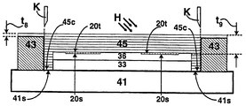
도 38에 있어서, 엠보싱 장치(200)는 코팅 측부(101c)와 기부 측부(101b)를 구비한 가요성 기판(101)을 포함한다. 코팅 유닛(300)은 코팅 측부(101c)상의 광중합체 재료(301)(도 42, 도 43 및 도 44 참조)를 적층하도록 작동한다. 광중합체 재료(301)는 제 1 두께(tc)를 갖는다. 엠보싱 가공 벨트(100)는 광학적으로 투명한 벨트 재료(81)와, 벨트 재료(81)와 접속하는 광학적으로 투명한 유연성 매체(70)를 포함한다(도 45 참조). 또한, 유연성 매체(70)는 임프린트 패턴(20q)(도 29 참조)을 구비한 광학적으로 투명한 임프린트 스탬프(20t)를 포함한다. 임프린트 패턴(20q)이 임프린트 스탬프(20t)와 동일한 재료로 형성되기 때문에, 임프린트 패턴(20q)도 광학적으로 투명하다. 도 45, 도 37a 및 도 37b에는 도 38 및 도 39에 도시한 것보다 상세하게 도시된 엠보싱 가공 벨트(100)가 제공되어 있다.In FIG. 38, the
복수의 반송 롤러(103)는 벨트 재료(81)와 접속하여 엠보싱 벨트(100)를 지지하도록 작동한다. 구동 유닛(110)은 구동 운동(WD)을 엠보싱 가공 벨트(100)와 가요성 기판(101)에 부여한다. 후술하는 바와 같이, 구동 유닛(110)은 구동 운동(WD)을 수행하기 위해 다양한 방식으로 엠보싱 장치(200)와 접속될 수 있다.The plurality of conveying
백킹 드럼(105)은 가요성 기판(101)의 기부 측부(101b)의 일부 및 유연성 매체(70)의 일부에 의해 감싸지고, 이에 의해 장력이 엠보싱 가공 벨트(100)와 가요성 기판(101)에 부여된다. 장력은 가요성 기판(101)과 엠보싱 가공 벨트(100) 사이의 압력을 발생시킨다. 광중합체 재료(301)내에 임프린트 스탬프(20t)의 엠보싱 가공을 수행하도록 압력이 작동한다. 기부 측부(101b)를 백킹 드럼(105) 위로 이송하고 임프린트 스탬프(20t)와 코팅 측부(101c)를 서로 접촉하게 가압하도록 회전력(DR)이 작동되어, 임프린트 패턴(20q)이 광중합체 재료(301)내에 엠보싱 가공되고 광중합체 재료(301)내에 복제 패턴(20u)(도 47 참조)을 형성한다.The
자외선 광원(99)은 벨트 재료(81)와 임프린트 스탬프(20t)를 통해서 복제 패턴(20u)에 자외선(L)을 조사한다. 복제 패턴(20u)에 대한 조사가 복제 패턴(20u)의 엠보싱 가공과 동시에 일어나, 복제 패턴(20u)은 경화하고, 그 형상을 유지한다. 복제 패턴(20u)은 마스터 기판(11)상의 패턴(20p)을 보완하는 그 내의 복수의 패턴(20v)을 포함한다(도 5 및 도 6 참조).The ultraviolet
자외선 광원(99)은, 임프린트 패턴(20q)이 광중합체 재료(301)내에 엠보싱 가공되기 전에 광중합체 재료(301)가 자외선(L)에 의해 경화되지 않도록 임프린트 스탬프(20t)가 코팅 측부(101c)와 접촉하게 가압되는 지점에 자외선(L)의 초점을 맞추는 반사기(99r)를 포함할 수 있다. 도 45에 있어서, 반사기(99r)(도시하지 않음)는 복제 패턴(29u)이 엠보싱 가공되는 것과 거의 동시에 경화되는 영역에 자외선(L)의 초점을 맞추는 경화 윈도우(curing window)(CW)를 형성한다. 또한, 반사기(99r)는 자외선(L)의 누설을 방지하도록 작동할 수 있는데, 이 자외선이 누설되면 광중합체 재료(301)상에 잠재적으로 충돌해서, 임프린트 스탬프(20t)에 의해 광중합체 재료(301)가 엠보싱 가공되기 전에 자외선이 광중합체 재료(301)를 경화시킬 수도 있다.The ultraviolet
본 발명의 하나의 이점은, 복제 패턴(20u)의 조사가 가요성 기판(101)을 통하지 않고 엠보싱 가공 벨트(100)를 통해 일어나므로, 가요성 기판(101)이 자외선(L)에 불투명한 경우 광중합체 재료(301)를 엠보싱 가공하고 경화하는 단계에서 엠보싱 장치(200)가 효과적인 것이다. 따라서, 본 발명의 엠보싱 장치(200)는 불투명 가요성 기판(101) 또는 광학적으로 투명한 가요성 기판(101)상의 광중합체 재료(301)를 엠보싱 가공하고 경화하는데 이용될 수 있다. 어떤 응용예에서는 가요성 기판(101)용 재료가 불투명 재료인 것을 요구할 것이기 때문에, 본 발명의 엠보싱 장치(200)는 가요성 기판(101)의 재료 선택에 있어서 융통성을 허용한다.One advantage of the present invention is that the irradiation of the
자외선 광원(99)은, 약 0.1초 내지 약 6.0초 정도인 매우 짧은 시간 내에 복제 패턴(20u)을 경화하는 것이 바람직하기 때문에, UVA 자외선 광원일 수 있으며, 바람직하게는 산업용 등급의 UVA 광원일 수도 있다. 자외선(L)은 약 300.0㎚ 내지 약 400.0㎚의 파장을 갖는 것이 바람직하다. 또한, 자외선 광원(99)용 강도는 적용에 따르지만, 예로서 약 200.0mW/cm2 내지 약 1000.0mW/cm2 범위의 강도가 이용될 수 있다. 다른 예로서, 놀랜드(Norland)(등록상표) 광학 접착제가 경화를 위해 약 0.2J/cm2의 총 에너지를 필요로 한다.The ultraviolet
광중합체 재료(301)에 대한 조사가 엠보싱 가공 벨트(100)를 통해 일어난다는 점에서, 자외선 광원(99)은 도 39 및 도 45에 도시한 바와 같은 엠보싱 가공 벨트(100) 내부의 위치와, 도 38 및 도 45에 도시한 바와 같은 엠보싱 가공 벨트(100) 외부의 위치를 포함하는 엠보싱 가공 벨트(100)에 대한 위치를 가질 수 있다. 자외선 광원(99)이 도 38에서와 같이 엠보싱 가공 벨트(100) 외부에 위치된 경우, 자외선 광원(99)이 엠보싱 가공 벨트(100) 내부에 위치된 경우의 1개 층에 비해서, 자외선(L)이 엠보싱 가공 벨트(100)의 2개 층을 통과함으로 인한 자외선(L) 강도가 약간 감쇠되는 것을 고려할 필요가 있을 수도 있다. 따라서, 자외선 광원(99)이 엠보싱 가공 벨트(100) 외부에 위치된 경우보다 높은 강도의 자외선 광원(99)을 이용할 필요가 있다.In that the irradiation of the
도 39에 있어서, 엠보싱 가공 벨트(100) 내부상에 자외선 광원(99)을 수용하는 공간을 형성하기 위해 3개의 반송 롤러(103)가 이용된다. 그러나, 유연성 매체(70)가 임의의 크기일 수 있기 때문에, 자외선 광원(99)을 수용하기에 충분히 큰 공간을 형성하기 위해, 엠보싱 가공 벨트(100)를 보다 크게 제조하고 반송 롤러(103)의 직경을 보다 크게 제조하는 단계를 포함하는 엠보싱 가공 벨트(100) 내부상에 자외선 광원(99)을 수용하기 위한 다양한 방식이 있다. 따라서, 도 39의 실시예는 단지 엠보싱 가공 벨트 내부상에 자외선 광원(99)을 수용하는 방법에 대한 예시이고, 또한 다른 구성도 가능하며, 본 발명은 도 39에 도시한 구성에 제한되지 않는다.In FIG. 39, three conveying
도 42에 있어서, 코팅 유닛(300)은 제 1 두께(tc)를 갖는 코팅 측부(101c)상에 광중합체 재료(301)를 적층하도록 작동한다. 전형적으로, 광중합체 재료(301)는 코팅 측부(101c)상에 적층하기 전에 액체 형상(301L)으로 공급된다. 구동 운동(WD)시, 코팅 측부(101c)와 코팅 유닛(300) 사이의 코팅 거리(Dc)가 정확하게 유지되어, 제 1 두께(tc)가 변경되지 않고 광중합체 재료(301)가 코팅 측부(101c)상에 매끄럽고 균일한 층으로서 적층되는 것이 중요하다. 광중합체 재료(301)에는, 이에 제한되지 않지만 자외선에 노출될 때 경화되는 놀랜드(등록상표) 광학 접착제가 포함된다. 바람직하게는, 광중합체 재료는 약 0.1초 내지 약 6.0초의 시간에 경화될 것이다. 예를 들면, 놀랜드(등록상표) NOA 83H 광중합체가 광중합체 재료(301)용으로 이용될 수 있다. 또한, 광중합체 재료(301)는 포토레지스트 재료일 수도 있다.In FIG. 42, the
경우에 따라, 엠보싱 장치(200)는 코팅 측부(101c)와 코팅 유닛(300) 사이에서 일정 거리(Dc)를 유지하도록 작동하는 가이드 롤러(109)를 포함하여, 광중합체 재료(301)의 제 1 두께(tc)가 정확하게 유지될 수 있다. 공급 릴(supply reel)(107s)이 가요성 기판(101)을 이송 및 분배하는데 이용되는 경우 가이드 롤러(109)가 특히 유용하다. 가요성 기판(101)이 공급 릴(107s)을 감을 때, 코팅 유닛(300)으로부터의 거리는 변경될 수 있으며, 가요성 기판(101)이 공급 릴(107s)로부터 풀림에 따라 가요성 기판(101)의 권취된 직경이 감소될 때 코팅 유닛(300)으로부터의 거리가 증가할 것이다. 따라서, 가이드 롤러(109)가 코팅 측부(101c)와 코팅 유닛(300) 사이의 거리를 제어한다.In some cases, the
광중합체 재료(301)의 제 1 두께(tc)는 용도에 따를 것이며, 코팅 유닛(300)의 유형도 용도에 따를 것이다. 엠보싱 가공된 층의 후속 에칭을 위한 엠보싱 잔류물을 최소화하기 위해, 제 1 두께(tc)는 전형적인 형상 높이(도 4에서의 ho 참조)와 대체로 유사하다. 예를 들면, 임프린트 스탬프(20t)가 나노미터(㎚) 크기(예컨대, 1.0㎛ 미만, 바람직하게는 100.0㎚ 미만)를 갖는 임프린트 패턴(20q)을 포함한다면, 광중합체 재료(301)의 매우 얇은 층을 적층하는 것이 바람직하다. 바람직하게는, 제 1 두께(tc)는 약 0.05㎛ 내지 약 2.0㎛의 범위에 있다.The first thickness t c of the
광중합체 재료(301)의 균일하고 얇은 층을 적층할 수 있으며 코팅 유닛(300)용으로 이용될 수 있는 코팅 기술에는, 이에 제한되지 않지만 그라비어 코팅기, 마이크로 그라비어(등록상표) 코팅기(Micro Gravure Coater), 및 슬롯 다이 코팅기(Slot Die Coater)가 포함된다. 예를 들면, 제 1 두께(tc)용으로 상기 언급된 두께 범위는 야스이 세이키(Yasui Seiki)(등록상표) 마이크로 그라비어(등록상표) 코팅기를 이용하여 얻어질 수 있다. 광중합체 재료(301)는 아세톤 등의 용질로 박형화되어 제 1 두께(tc)용의 보다 얇은 코팅을 성취할 수 있다.Coating techniques that can deposit a uniform, thin layer of
도 43에 있어서, 코팅 유닛(300)은 그라비어 코팅기 또는 마이크로 그라비어(등록상표) 코팅기일 수 있다. 한 쌍의 롤러(303r)는 액체 광중합체 재료(301L)를 수용하는 용기(tub)(303s)내에서 회전하는 조각식 드럼(engraved drum)(303g) 위의 가요성 기판(101)의 코팅 측부(101c)의 일부를 균일하게 감싼다. 광중합체 재료(301L)는 드럼(303g)의 표면상의 패턴상에 모인다. 닥터 블레이드(doctor blade)(303d)는 광중합체 재료(301L)의 초과량을 닦아 내어 얇고 균일한 막이 코팅 측부(101c)상에 적층된다. 바람직하게는, 마이크로 그라비어(등록상표) 코팅기가 그라비어 코팅기의 직경보다 작은 직경을 갖는 드럼(303g)을 가지므로 마이크로 그라비어(등록상표) 코팅기가 이용되고, 광중합체 재료(301)의 초박막을 적층하는데 보다 적합하다.In FIG. 43, the
선택적으로, 도 44에 있어서, 슬롯 다이 코팅기가 광중합체 재료(301)를 적층하는데 이용될 수 있다. 액체 광중합체 재료(301L)는 한 쌍의 다이 립(die lip)(301D)에 의해 형성된 다이 슬롯(301S)으로 압력하에서 공급(Sf)된다. 다이 립(301D)은 가요성 기판(101)의 두께(ts)를 포함하는 코팅 갭(tG)에 의해 가요성 기판(101) 위에 위치된다. 가요성 기판(101)의 코팅 측부(101c)가 다이 슬롯(301S) 아래를 통과할 때, 액체 광중합체 재료(301L)는 코팅 측부(101c)를 제 1 두께(tc)로 코팅한다.Optionally, in FIG. 44, a slot die coater can be used to deposit the
구동 운동(WD)은 코팅 분야 및 기계 분야에서 잘 이해되는 각종 기법을 이용하여 성취될 수 있다. 예시로서, 도 38에 있어서, 구동 유닛(110)은 상술한 바와 같이 엠보싱 가공되고 경화된 후에 가요성 기판(101)을 수집하도록 작동하는 테이크업 릴(takeup reel)(107r)과 기계식으로 연통한다.The drive movement W D can be achieved using various techniques well understood in the coating field and the mechanical field. As an example, in FIG. 38, the
테이크업 릴(107r)은 회전력(DR)을 테이크업 릴(107r)에 부여하는 구동 벨트(110b)를 이용하여 구동 유닛(110)과 접속되며, 이 구동 유닛(110)은 테이크업 릴(107r)상에 가요성 기판(101)을 수집하고 구동 운동(WD)을 가요성 기판(101) 및 엠보싱 가공 벨트(100)에 부여할 수 있다. 구동 벨트(110b)가 도시되어 있지만, 기어, 직접 드라이브, 풀리, 샤프트 등을 포함하는 구동력을 기계식으로 전달하기 위한 수단이 이용될 수 있다. 구동 유닛(110)은 예를 들어 전기 모터일 수 있다.The take-up
하나 또는 그 이상의 구동 유닛(110)이 구동 운동(WD)을 부여하는데 이용될 수 있으며, 이들 구동 유닛(110)이 하나 또는 그 이상의 반송 롤러(103) 등의 엠보싱 장치(200)의 하나 또는 그 이상의 구성요소와 접속되어, 구동 유닛(110)은 반송 롤러(103)를 회전시켜서, 가요성 기판(101) 및 엠보싱 가공 벨트(100)에 구동 운동(WD)을 부여할 수 있다.One or
유연성 매체(70)는 도 1 내지 도 37b를 참조하여 후술되는 바와 같이 광학적으로 투명한 트랜스퍼 접착제에 적층된 광학적으로 투명한 실리콘계의 탄성중합체 재료로 이루어질 수 있다. 실리콘계 탄성중합체 재료[도 22에서의 참조부호(44) 참조]로 적합한 재료에는, 이에 제한되지 않지만 폴리디메틸 실록산(PDMS), 실가드(SYLGARD) 182(등록상표) 실리콘 탄성중합체, 실가드 183(등록상표) 실리콘 탄성중합체, 실가드 184(등록상표) 실리콘 탄성중합체 및 실가드 186(등록상표) 실리콘 탄성중합체를 포함하는 다우 코닝(DOW CORNING)(등록상표) 실리콘계 컨포멀(conformal) 코팅이 포함된다.The
트랜스퍼 접착제 층[도 27에서의 참조부호(51) 참조]에 적합한 광학적으로 투명한 재료에는, 이에 제한되지 않지만 어드헤시브 리서치 인코포레이티드(Adhesives Research, Inc)(등록상표)의 아클리어(ARclear)(등록상표) DEV-8932 광학적으로 투명한 실리콘 접착제가 포함된다. 예를 들면, 아클리어(등록상표) DEV-8932의 25.0㎛ 두께의 시트(즉, 제 7 두께 t7 = 25.0㎛)가 트랜스퍼 접착제 층(51)용으로 이용될 수 있다.Suitable optically transparent materials for the transfer adhesive layer (see
벨트 재료(81)는 광(L)이 벨트 재료(81), 유연성 매체(70) 및 임프린트 스탬프(20t)를 통과할 수 있는 광학적으로 투명한 재료일 수 있다. 밸트 재료(81)용으로 적합한 광학적으로 투명한 재료에는, 이에 한정되지는 않지만 폴리에스테르 필름 및 마일라(Mylar)(등록상표)가 포함된다. 벨트 재료(81)의 두께가 적용에 기초하여 변경되지만, 유연성 매체(70)와 접속시 가요성 벨트가 되는 벨트 재료(81)의 두께의 적당한 범위는 약 50.0㎛ 내지 약 150.0㎛이다.
본 발명의 변경 실시예에 있어서, 도 40, 도 41 및 도 46에 도시한 바와 같이, 엠보싱 장치(200)는 전술한 엠보싱 가공 벨트(100) 대신에 엠보싱 가공 드럼을 포함한다. 엠보싱 장치(200)는 가요성 기판(101)과, 코팅 유닛(300)과, 광학적으로 투명한 실린더(69) 및 실린더(69)와 접속하는 광학적으로 투명한 유연성 매체(70)를 구비한 엠보싱 가공 드럼(90)을 포함한다. 상술한 바와 같이, 유연성 매체(70)는 그 내에 임프린트 패턴(20q)을 갖는 광학적으로 투명한 임프린트 스탬프(20t)를 포함한다. 도 46 및 도 32 내지 도 34b는 도 40 및 도 41에 도시한 것보다 엠보싱 가공 드럼(90)을 상세하게 제공하고 있다.In an alternative embodiment of the invention, as shown in FIGS. 40, 41 and 46, the
또한, 상술한 바와 같이, 구동 유닛(110)은 구동 운동(WD)을 엠보싱 가공 드럼(90) 및 가요성 기판(101)에 부여한다. 엠보싱 장치(200)는 일정 거리(DC)를 유지하기 위한 상술된 가이드 롤러(109)와, 공급 릴(107s)과, 테이크업 릴(107t)을 포함한다. 구동 유닛(110)은 테이크업 릴(107t) 및/또는 하나 또는 그 이상의 반송 롤러(103)를 구동할 수 있다. 선택적으로, 엠보싱 가공 드럼(90)은 구동 유닛(110)에 의해 구동되지만, 유연성 매체(70)와 가요성 기판(101) 사이의 미끄럼이 회피되도록 주의가 취해져야 한다.In addition, as described above, the
복수의 반송 롤러(103)는 가요성 기판(101)의 기부 측부(101b)와 접속하고, 엠보싱 가공 드럼(90)의 일부 위에 코팅 측부(101c)를 균일하게 감싸도록 작동하여 엠보싱 가공 드럼(90)이 가요성 기판(101)에 장력을 부여하고 장력은 가요성 기판(101)과 엠보싱 가공 드럼(90) 사이에 압력을 발생시킨다. 광중합체 재료(301)내에 임프린트 스탬프(20t)의 엠보싱 가공을 수행하도록 압력이 작용한다.The plurality of conveying
구동 운동(WD)은 엠보싱 가공 드럼(90) 위로 코팅 측부(101c)를 전송하고 코팅 측부(101c)와 접촉하도록 임프린트 스탬프(20t)를 가압하여 광중합체 재료(301)내에 복제 패턴(20u)을 형성하기 위해 광중합체 재료(301)내에 임프린트 패턴(20q)이 엠보싱 가공된다. 도 46에 있어서, 유연성 매체(70)는 엠보싱 가공 드럼(90)의 외부 표면을 형성하여 가요성 기판(101)이 엠보싱 가공 드럼(90)의 감싸진 일부 위에 전송될 때 코팅 측부(101c)가 유연성 매체(70) 및 임프린트 스탬프(20t)를 접촉하게 된다.The drive motion W D transmits the
자외선 광원(99)은 실린더(69)와 임프린트 스탬프(20t)를 통과한 자외선(L)을 복제 패턴(20u)에 조사한다. 복제 패턴(20u)의 조사는 복제 패턴(20u)의 엠보싱 가공과 동시에 일어난다.The ultraviolet
전술한 바와 같이, 가요성 기판(101)은 자외선(L)에 불투명일 수 있다. 도 40, 도 41 및 도 46에 있어서, 자외선 광원(99)은 엠보싱 가공 드럼(90) 내부 또는 엠보싱 가공 드럼(90) 외부에 위치될 수 있다. 자외선(L)이 실린더(69)와 유연성 매체(70)의 2개의 층을 통과해야 하고 약간의 자외선(L) 감쇠가 일어나기 때문에 엠보싱 가공 드럼(90) 외부에 자외선 광원(99)이 위치된 경우 자외선 광원(99)의 강도를 증가시킬 필요가 있을 수 있다.As described above, the
자외선 광원(99)은 상술한 바와 같이 반사기(99r)를 포함할 수 있고 반사기(99r)는 경화 윈도우(Cw)(도 46 참조)를 형성할 수 있다. 자외선 광원(99)은 UVA 광원일 수 있고, 자외선(L)은 약 300.0㎚ 내지 약 400.0㎚의 파장을 가질 수 있다.The ultraviolet
엠보싱 가공 벨트(100)용으로 상술된 바와 동일한 재료가 엠보싱 가공 드럼(90)용으로 이용될 수 있지만, 실린더(69)는 이에 제한되지는 않지만 유리, 플라스틱 및 석영을 포함하는 광학적으로 투명한 재료일 수 있다.While the same material as described above for the
전술한 그라비어 코팅기, 마이크로 그라비어(등록상표) 코팅기 또는 슬롯 다이 코팅기가 코팅 유닛(300)용으로 이용될 수 있고, 광중합체 재료(301)의 제 1 두께(tc)는 약 0.5㎛ 내지 약 1.0㎛의 범위일 수 있다.The gravure coater, micro gravure® coater or slot die coater described above can be used for the
엠보싱 가공 벨트(100) 및 엠보싱 가공 드럼(90)은 도 1 내지 도 37b를 참조하여 후술된 방법을 이용하여 제조될 수 있다.The
도 1 내지 도 4에 있어서, 마스터 기판(11)은 그 내에 임프린트 패턴(20)을 형성하기 위해 패터닝된 다음 에칭된다. 도 1에 있어서, 마스터 기판(11)은 에칭 마스크(etch mask)로서 기능을 하는 재료(155)로 코팅된다. 재료(155)는 마이크로 전자공학 기술에서 보통 이용되는 포토레지스트 재료일 수 있다. 마스터 기판(11)내에 형성될 패턴(153)을 갖는 마스크(151)에 광(154)이 조명되는데, 재료(155)는 패턴(153)으로 광(154)에 노출된다.1-4, the
도 2에 있어서, 재료(155)는 광(154)에 노출되었던 재료(155)의 일부를 제거하도록 현상된다. 도 2 및 도 3에 있어서, 마스터 기판(11)은 재료(155)로 덮이지 않은 마스터 기판(11)의 일부를 제거하도록 에칭 물질로 에칭된다. 결과로서, 도 3에 있어서, 복수의 임프린트 패턴(20p)은 마스터 기판(11)내에 형성된다. 도 4에 있어서, 임프린트 패턴(20p)은 마스터 기판(11)상에 임프린트 스탬프(20)를 규정한다.In FIG. 2,
임프린트 스탬프(20)는 폭, 길이 및 높이의 모든 3차원 치수가 변경되는 임프린트 패턴(20p)을 포함할 수 있다. 도 4의 단면도 및 도 5의 평면도에 있어서, 임프린트 패턴(20p)은 폭 치수(d0), 높이 치수(h0) 및 길이 치수(L0)가 변경된다. 임프린트 패턴(20p)의 실제 치수는 적용에 따를 것이고, 재료(155)를 패터닝하기 위해 이용되는 리소그래피 공정에 많이 따를 것이다. 예를 들면, 최신의 마이크로 전자공학 리소그래피 공정이 이용된 경우, 치수(d0, h0, L0)는 서브-마이크로미터 크기, 즉 1.0㎛ 미만일 수 있다. 예를 들면, 임프린트 패턴(20p)은 100.0㎚ 이하의 치수(d0, h0, L0)를 가질 수 있는 임프린트 패턴(20p)을 갖는 나노-임프린트 패턴일 것이다. 따라서, 임프린트 패턴(20)은 나노미터 크기의 치수(d0, h0, L0)를 갖는 임프린트 패턴(20p)을 갖는 나노-임프린트 스탬프일 것이다.The
마이크로 전자공학 기술에서 잘 이해되는 리소그래피 공정이 마스터 기판(11)을 패터닝하고 에칭하는데 이용될 수 있다. 예를 들면, 재료(155)용 포토레지스트를 이용하는 포토리소그래피 공정 및 반응성 이온 에칭(reactive ion etching : RIE)과 같은 에칭 공정은 마스터 기판(11)내에 임프린트 스탬프(20)를 형성하는데 이용될 수 있다.Lithography processes, which are well understood in microelectronics techniques, can be used to pattern and etch the
마스터 기판(11)용으로 적합한 재료에는, 이에 제한되지는 않지만 실리콘(Si) 기판 및 실리콘(Si) 웨이퍼가 포함된다. 도 5에 있어서, 마스터 기판(11)은 웨이퍼 플랫(11F)을 갖는 실리콘 웨이퍼이다. 임프린트 스탬프(20)중 4개가 마스터 기판(11)내에 형성된다. 실리콘 웨이퍼는 임의의 크기일 수 있다. 예를 들어 4.0인치 실리콘 웨이퍼가 임프린트 스탬프(20)중 4개에 대해 마스터 기판(11)으로서 이용되었다. 보다 큰 직경의 실리콘 웨이퍼(예컨대, 8인치 또는 12인치)는 보다 많은 임프린트 패턴(20p) 또는 보다 큰 임프린트 스탬프(20)를 위한 보다 큰 표면적을 제공하도록 이용될 수 있다. 임프린트 패턴(20p)이 도 5에 동일하게 나타나 있지만, 임프린트 스탬프(20)는 임프린트 스탬프(20)중 변경되는(즉, 동일하지 않은) 임프린트 패턴(20p)을 포함할 수 있다.Suitable materials for the
도 6에 있어서, 해제 층(13)은 임프린트 패턴(20p) 위에 적층된다. 해제 층(13)은 제 1 두께(t1)가 임프린트 패턴(20p)의 수직 및 수평 표면상에 실질적으로 동일하도록 임프린트 패턴(20p)을 균일하게 코팅하게 작동하는 제 1 두께(t1)를 포함한다. 해제 층(13)용으로 적합한 재료에는, 이에 제한되지는 않지만 플루오로카본 재료가 포함된다. 예로서, 해제 층(13)용 플루오로카본 재료는 약 5.0분 동안 트리플루오로메탄(CHF3)의 플라즈마 적층법을 이용하여 적층될 수 있다.In FIG. 6, the
제 1 두께(t1)는 적용에 따라 다르지만, 후술하는 바와 같이 해제 층(13)은 이후에 해제 층(13)으로부터 해제될 실리콘계 탄성중합체 재료를 적용하는 비접착면을 제공하도록 작동한다. 따라서, 해제 층(13)은 약 50.0㎚ 내지 약 150.0㎚인 제 1 두께(t1)를 갖는 매우 얇은 층일 수 있다.The first thickness t 1 depends on the application, but as will be described later the
도 7에 있어서, 실리콘계 탄성중합체 층(15)은 해제 층(13) 위에 임프린트 패턴(20p)을 완전히 덮는 제 1 깊이(d1)에 적층된다. 실리콘계 탄성중합체 층(15)을 위해 균일한 두께를 얻기 위해, 마스터 기판(11)은 실질적으로 평탄해야 한다. 이것은, 예컨대 실리콘계 탄성중합체 층(15)을 적층하기 전에 마스터 기판(11)을 수평면 또는 수평한 진공 척 상에 위치시킴으로써 성취될 수 있다.In FIG. 7, the silicone-based
그 후, 실리콘계 탄성중합체 층(15)이 마스터 기판(11)을 가열(H)함으로써 경화된다. 이 경화는 소정의 시간 동안 소정의 온도에서 마스터 기판(11)을 구움(baking)으로써 성취될 수 있다. 실제 시간 및 온도는 적용에 따라 다르며, 실리콘계 탄성중합체 층(15)용으로 이용되는 재료의 유형에도 의존할 것이다. 실리콘계 탄성중합체 층(15)용으로 적합한 재료에는, 이에 제한되지는 않지만 폴리디메틸 실록산(PDMS)과, 실가드 183(등록상표) 실리콘계 탄성중합체, 실가드 184(등록상표) 실리콘계 탄성중합체, 실가드 186(등록상표) 실리콘계 탄성중합체를 포함하는 다우 코닝(등록상표) 실리콘계 컨포멀 코팅이 포함된다.Thereafter, the silicone-based
실리콘계 탄성중합체 층(15)의 제 1 깊이(d1)는 적용에 따라 다를 것이다. 그러나, 바람직한 실시예에 있어서, 실리콘계 탄성중합체 층(15)의 제 1 깊이(d1)는 약 0.5㎜ 내지 약 1.5㎜이다. PDMS 또는 다우 코닝(등록상표) 실가드(등록상표) 실리콘 탄성중합체에 대해, 실리콘계 탄성중합체(15)의 경화는 오븐 등에서 마스터 기판(11)을 구움으로써 성취될 수 있다. 소정의 온도 및 소정의 경화 시간은 약 100.0℃의 온도에서 약 4.0시간 동안일 수 있다.The first depth d 1 of the silicone-based
도 6에 도시한 변경 실시예에 있어서, 상술된 경화 단계 전에, 제 2 두께(t2)를 갖는 커버 층(16)은 이미 적층된 실리콘계 탄성중합체 층(15) 위에 적용된다. 바람직하게는, 커버 층(16)은 폴리에스테르 필름이고, 제 2 두께(t2)는 약 50.0㎛ 내지 약 150.0㎛이다. 커버 층(16)은 실리콘계 탄성중합체 층(15)의 실질적으로 편평한 표면(15s)으로부터의 편차를 야기하는 실리콘계 탄성중합체 층(15)에서의 임의의 표면 변형을 편평화하는데 이용될 수 있다.In the alternative embodiment shown in FIG. 6, before the curing step described above, a
경화 단계 후에, 임프린트 패턴(20p)의 보완적인 이미지는, 임프린트 스탬프(20a)가 실리콘계 탄성중합체 층(15)내에 형성되도록 실리콘계 탄성중합체 층(15)내에서 복제(20r)된다(도 8 내지 도 10 참조).After the curing step, the complementary image of the
도 7에 있어서, 경화 단계 후에, 실리콘계 탄성중합체 층(15)은 해제 층(13)으로부터 해제된다. 한 쌍의 트위저(tweezer)의 팁 혹은 X-Acto(등록상표) 나이프와 같은 나이프 또는 면도기의 에지는, 나이프 에지(K)와, 실리콘계 탄성중합체 층(15)과 해제 층(13) 사이에 삽입된 점선 화살표에 의해 도시한 바와 같이, 실리콘계 탄성중합체 층(15)을 해제 층(13)으로부터 분리하는데 이용될 수 있다. 그 다음, 실리콘계 탄성중합체 층(15)은 실리콘계 탄성중합체 층(15)의 에지를 잡아 해제 층(13)으로부터 실리콘계 탄성중합체 층(15)을 벗겨 냄으로써[점선 화살표(P) 참조] 해제 층(13)이 들리게 될 수 있다. 상기 언급된 커버 층(16)이 이용된 경우, 커버 층(16)은 실리콘계 탄성중합체 층(15)이 해제 층(13)으로부터 해제되기 전에 실리콘계 탄성중합체 층(15)으로부터 제거된다.In FIG. 7, after the curing step, the silicone-based
도 8 내지 도 10에 있어서, 임프린트 스탬프(20a)는, 임프린트 스탬프(20a)를 에워싸는 실리콘계 탄성중합체 층(15)의 초과 부분으로부터 제거된다. 상기 언급한 커버 층(16)이 이용된 경우, 임프린트 스탬프(20a)는, 임프린트 스탬프(20a)를 에워싸는 실리콘계 탄성중합체 층(15) 및 커버 층(16)의 초과 부분으로부터 제거된다.8-10, the
모든 경우에 있어서, 임프린트 스탬프(20a)는 실리콘계 탄성중합체 층(15)을 실질적으로 편평한 기판(21)상에 위치시키고, 그 후 임프린트 스탬프(20a)의 주변부(도 8 및 도 9에서의 점선 라인 참조) 둘레에 절단부(C)를 위치시켜 실리콘계 탄성중합체 층(15)의 초과 부분 또는 실리콘계 탄성중합체 층(15) 및 커버 층(16)을 임프린트 스탬프(20a)로부터 해제함으로써 그 초과 부분으로부터 제거된다. 나이프, 면도기, 다이 등은 도 9에서의 나이프(K)에 의해 도시된 바와 같이 절단부(C)를 성취하는데 이용될 수 있다. 임프린트 스탬프(20a)가 해제된 후에, 초과 부분(15, 또는 15 및 16)은 실질적으로 편평한 기판(21)으로부터 벗겨져 나가 임프린트 스탬프(20a)가 초과 부분과 더 이상 접속되지 않을 수 있다(도 10 참조). 실질적으로 편평한 기판(21)은, 이에 제한되지는 않지만 유리, 금속, 플라스틱 및 석영을 포함하는 재료일 수 있다. 예를 들면, 실질적으로 편평한 기판(21)은 유리판일 수 있다.In all cases, the
경우에 따라, 상기 언급된 단계는 마스터 기판(11)을 이용하는 추가적인 임프린트 스탬프(20a)를 제조하는데 필요한 바와 같이 반복될 수 있다. 본 발명의 방법의 하나의 이점은 마스터 기판(11)이 전술한 프로세스 단계에 의해 손상되지 않는 점이다. 결과적으로, 동일 마스터 기판(11)은 몇 개의 임프린트 스탬프(20a)를 제조하는데 반복적으로 이용될 수 있다. 따라서, 마스터 기판(11)을 패터닝 및 에칭하고 해제 층(13)을 적층하는 비용은 몇 개의 임프린트 스탬프(20a)를 지나 상환될 수 있다.In some cases, the above-mentioned steps may be repeated as necessary to manufacture the
본 발명의 방법의 다른 이점은 실리콘계 탄성중합체 층(15)이 입자 주위를 유동하고 입자를 비말 동반하기 때문에, 먼지 입자 등의 오염 물질을 제거하기 위해서 마스터 기판(11)이 각각의 사용 후에 세정될 필요가 없다는 점이다. 결과적으로, 마스터 기판(11)은 입자가 실리콘계 탄성중합체 층(15)과 함께 제거되기 때 문에 셀프 클리닝된다.Another advantage of the method of the present invention is that since the silicone-based
도 11에 있어서, 제 3 두께(t3)를 갖는 편평하고 얇은 플라스틱 필름(33)은 제 4 두께(t4)를 갖는 편평한 유연성 실리콘 고무 백킹(31)상에 위치된다. 얇은 플라스틱 필름(33)에 적합한 재료에는, 이에 한정되지는 않지만 폴리이미드 및 폴리에스테르(PET : 폴리에틸렌 테레프탈레이트)가 포함된다. 제 3 두께(t3) 및 제 4 두께(t4)는 적용에 따라 다를 것이다. 바람직하게는, 얇은 플라스틱 필름(33)의 제 3 두께(t3)는 약 40.0㎛ 내지 약 100.0㎛이고, 실리콘 고무 백킹(31)의 제 4 두께(t4)는 약 0.125인치 내지 약 0.25인치이다. 실리콘 고무 백킹(31)의 제 4 두께(t4)는 실리콘 고무 백킹(31)이 유연하게(즉, 딱딱하지 않게) 보증하도록 선택되어야 한다.In FIG. 11, a flat thin
도 12에 있어서, 얇은 플라스틱 필름(33)의 표면(33s)은 광중합체 용액(35)으로 코팅된다. 광중합체 용액(35)은, 이에 제한되지는 않지만 약 50%의 광중합체 재료 및 약 50%의 아세톤의 혼합물이다. 후술하는 바와 같이, 아세톤은 얇은 플라스틱 필름(33)의 표면(33s)상에 실질적으로 광중합체 층을 남긴 채 증발할 것이다. 광중합체 재료는 이에 제한되지는 않지만 자외선에 노출시 경화되는 놀랜드(등록상표) 광학 접착제가 포함될 수 있다. 바람직하게는, 광중합체 재료는 약 5.0초 내지 약 60.0초 시간내에 경화될 것이다. 예를 들면, 놀랜드(등록상표) NOA 83H 광중합체는 광중합체 용액(35)용으로 이용될 수 있다.In FIG. 12, the
도 13 및 도 14에 있어서, 광중합체 용액(35)은 얇은 플라스틱 필름(33)의 표면(33s) 위에 퍼져 제 5 두께(t5)를 갖는 광중합체 층(35)을 형성한다. 바람직하게는, 광중합체 용액(35)의 스프레딩(spreading) 공정은 제 1 직경을 갖는 와이어(W1)로 권취된 마이어 바아(Mayer bar)(M1)를 이용하여 성취된다. 마이어 바아(M1)는 표면(33s) 위로 미끄럼 운동(S)하고 광중합체 용액(35)을 측정하여 제 5 두께(t5)를 갖는 광중합체 층(35)이 형성된다. 광중합체 용액(35)내의 어떠한 아세톤은 스프레딩 공정시 실질적으로 증발된다. 결과로서, 광중합체 층(35)은 상술한 바와 같이 광중합체 재료를 실질적으로 포함한다. 바람직하게는, 광중합체 층(35)의 제 5 두께(t5)는 약 5.0㎛ 내지 약 10.0㎛이다. 와이어(W1)의 제 1 직경은 적용에 따라 다를 것이다. 바람직하게는, 와이어(W1)의 제 1 직경은 약 50.0㎛ 내지 약 100.0㎛이다.13 and 14, the
도 15에 있어서, 임프린트 스탬프(20a)의 패터닝된 표면(21a)은 광중합체 층(35)상에 위치된다. 임프린트 스탬프(20a)를 광중합체 층(35)상에 위치시키는 단계는 임프린트 스탬프(20a)의 에지(e1)를 광중합체 층(35)과 접촉하게 위치시키는 단계와, 패터닝된 표면(21a)의 나머지 부분을 광중합체 층(35)과 접촉하게 점차적으로 낮추면서 에지(e1)를 고정하는 단계를 포함할 수 있다. 한 쌍의 트위저 또는 흡입 막대는 하강 단계를 성취하고 에지(e1)를 유지하도록 에지(e2)를 잡는데 이용될 수 있다. 선택적으로, 고무 롤러 등은 패터닝된 표면(21a)을 광중합체 층(35)과 접촉시키는 점진적인 하강 단계와 함께 이용될 수 있다.In FIG. 15, the
점진적인 하강 단계에서의 하나의 이점은, 결함을 야기할 수 있는 공기 방울이 광중합체 층(35)과 패터닝된 표면(20r) 사이에 가두어지지 않도록 광중합체 층(35)과 패터닝된 표면(20r) 사이에 포획된 공기가 치환된다.One advantage in the gradual descent step is that between the
본 발명의 방법의 다른 이점은 임프린트 스탬프(20a)가 광중합체 층(35)상에 일단 위치되면, 임프린트 스탬프(20a)는 광중합체 층(35)상의 소정 위치에 임프린트 스탬프(20a)를 위치시키기 위해 광중합체 층(35)의 표면(33s) 위에 플로팅(floating)될 수 있다[점선 화살표(F) 참조]는 것이다. 플로팅(F)은 트위저 또는 흡입 막대를 이용하여 수동으로 수행될 수 있고, 또는 플로팅(F)은 자동식일 수 있으며, 로봇 엔드 이펙터(robotic end effector)와 같은 정밀 기계 장치가 임프린트 스탬프(20a)를 정밀하게 위치시키는데 이용될 수 있다.Another advantage of the method of the present invention is that once the
도 16에 있어서, 광중합체 층(35)은, 광중합체 층(35)상에 임프린트 스탬프(20a)의 위치를 고정하고 임프린트 패턴(20r)의 이미지를 광중합체 층(35)에 전사하도록 경화된다. 광중합체 층(35)은 제 1 기간동안 광중합체 층(35)에 소정 강도의 자외선(UV)을 조사함으로써 경화된다. 광중합체 층(35)은 경화하여 단단해지고, 광중합체 층(35) 내로 전사된 임프린트 패턴(20r)의 이미지도 단단해져서 임프린트 패턴(20s)으로서 광중합체 층(35)내에 고정된다.In FIG. 16, the
자외선(UV)은, 이에 제한되지는 않지만 약 300.0㎚ 내지 약 400.0㎚의 범위를 포함하는 파장을 가질 수 있다. 자외선(UV)의 소정 강도는, 이에 제한되지는 않지만 약 150mW/cm2의 강도를 포함할 수 있다. 제 1 기간은, 이에 제한되지는 않지만 약 5.0초 내지 약 60.0초의 시간이 포함될 수 있다. 예를 들면, 자외선(UV)은 UVA 자외선 광원에서 나온 것일 수 있다.Ultraviolet (UV) light may have a wavelength including, but not limited to, in the range of about 300.0 nm to about 400.0 nm. The predetermined intensity of ultraviolet (UV) may include, but is not limited to, an intensity of about 150 mW / cm 2 . The first period may include, but is not limited to, a time of about 5.0 seconds to about 60.0 seconds. For example, ultraviolet (UV) may be from a UVA ultraviolet light source.
본 발명의 방법의 또 다른 이점은 광중합체 층(35)을 패터닝하는데 이용되는 임프린트 패턴(20a)이 변경될 수 있는 두께(도 16에서의 tA 및 tB 참조)를 가질 수 있고, 두께의 그러한 변경은 임프린트 패턴(20r)의 전송에 대한 정확성을 광중합체 층(35)의 임프린트 패턴(20s)에 영향을 미치지 않을 것이다. 두께(tA, tB)의 변경은 임프린트 스탬프(20a)를 제조하는데 이용된 고정의 변경, 도 7의 제 1 깊이(d1)의 변경 또는 다른 임프린트 패턴(20p)을 갖는 다른 임프린트 스탬프(20)를 제조하기 위한 다른 마스터 기판(11)의 사용에 기인할 수 있다.Another advantage of the method of the present invention is that the
경화 단계 후에, 도 17 및 도 18에 있어서, 임프린트 스탬프(20a)는 광중합체 층(35)으로부터 제거(P)하여, 임프린트 패턴(20r)의 이미지는 그 내에 고정된 임프린트 패턴(20s)을 갖는 광중합체 시임(36)을 규정한다. 임프린트 스탬프(20a)는 에지(e1 또는 e2)를 잡아 광중합체 층(35)으로부터 임프린트 스탬프(20a)를 들어올리기 위한 한 쌍의 트위저 등을 이용하여 제거(P)될 수 있다[점선 화살표(P) 참조].After the curing step, in FIGS. 17 and 18, the
도 19에 있어서, 광중합체 시임(36)을 가열함으로써 광중합체 시임(36)이 후경화된다. 광중합체 시임(36)의 후경화 단계는, 이에 제한되지는 않지만 약 100℃의 온도에서 약 1.0시간을 포함할 수 있다. 경우에 따라, 후경화 단계 후에, 광중합체 시임(36)은 PDMS 또는 상기 언급한 실가드(등록상표) 실리콘계 탄성중합체와 같은 실리콘계 탄성중합체 재료의 경화를 방해할 수 있는 화학종을 제거하기 위해 아세톤 용액으로 헹궈질 수 있다. 광중합체 시임(36)의 후경화는 경화 방해종을 없애고, 얇은 플라스틱 필름(33)에 광중합체 시임(36)의 고착을 향상시킨다.In FIG. 19, the
도 19에 있어서, 광중합체 시임(36)의 후경화에, 제 6 두께(t6)를 갖는 플루오로카본 재료(37)의 코팅은 광중합체 시임(36)상에 적층된다. 제 6 두께(t6)는 이에 제한되지는 않지만 약 50.0㎚ 내지 약 150.0㎚의 두께가 포함될 수 있다. 예로서, 플루오로카본 재료(37)은 약 5.0분 동안 트리플루오로메탄(CHF3)의 플라즈마 적층법을 이용하여 적층될 수 있다.In FIG. 19, upon post cure of the
또한, 도 19에 있어서, 플루오로카본 재료(37)의 적층 후에, 트위저 또는 나이프 에지는 얇은 플라스틱 필름(33)과 실리콘 고무 백킹(31) 사이에 삽입될 수 있고, 얇은 플라스틱 필름(33)은 점선 화살표(P)에 의해 나타낸 바와 같이 실리콘 고무 백킹(31)이 벗겨질 수 있다. 이하에, 광중합체 시임(36)과 얇은 플라스틱 필름(33)의 조합체는 달리 언급하지 않는다면 광중합체 시임(36)으로 지칭될 것이다.19, after lamination of the
도 20에 있어서, 얇은 플라스틱 필름(33)이 분리된 후에, 광중합체 시임(36)은 지지 기판(41)에 부착된다. 광중합체 시임(36)은 광중합체 시임(36)을 지지 기판(41)상에 놓고 접착제를 이용하여 광중합체 시임(36)의 단부를 지지 기판(41)에 고정함으로써 지지 기판(41)과 접속될 수 있다. 예를 들면, 고온 접착 테이프(T)가 이용될 수 있다. 지지 기판(41)은, 이에 제한되지는 않지만 유리 및 석영을 포함하는 재료로 이루어질 수 있다.In FIG. 20, after the
도 21 및 도 22에 있어서, 제 1 높이(h1)를 갖는 시임 스톡(43)은 지지 기판(41)에 부착된다. 시임 스톡(43)은, 예컨대 상기 언급된 고온 접착 테이프(T)와 같은 접착제를 이용하여 지지 기판(41)과 접속될 수 있다. 시임 스톡(43)은 광중합체 시임(36)에 인접하게 위치되고, 제 1 거리(D1)에 의해 광중합체 시임(36)으로부터 이격되어 지지 기판(41)의 표면(41s)상에 시임 스톡(43)과 광중합체 시임(36) 사이에 공간이 존재한다. 시임 스톡(43)의 제 1 높이(h1)는 도 22에 도시한 바와 같이 광중합체 시임(36)의 높이(hs) 이상이어야 한다. 제 1 높이(h1) 및 제 1 거리(D1)는 적용에 따라 다를 것이지만, 제 1 높이(h1)는 이에 제한되지는 않지만 약 0.5㎜ 내지 약 1.5㎜를 포함하는 범위일 수 있고, 제 1 거리(D1)는 이에 제한되지는 않지만 약 1.0㎜ 내지 약 2.0㎜를 포함하는 범위일 수 있다. 시임 스톡(43)은 이에 제한되지는 않지만 금속, 유리, 석영 및 스테인리스강을 포함하는 재료일 수 있다. 예를 들면, 시임 스톡(43)은 스테인리스강 시임 스톡일 수 있고, 제 1 높이(h1)는 약 0.5㎜일 수 있다.In FIGS. 21 and 22, a
도 21에 있어서, 지지 기판(41)은, 후술하는 바와 같이 시임 스톡(43) 및 실리콘계 탄성중합체 재료를 갖는 광중합체 시임(36)의 코팅의 준비에 있어서 지지 기판(41)의 온도를 증가시키기 위해 예열(H)된다. 바람직하게는, 실리콘계 탄성중합체 재료는 냉간 지지 기판(41) 또는 실온(즉, 약 18.0℃ 내지 약 28.0℃) 지지 기판상에 코팅되지 않는다. 지지 기판(41)을 위한 예열 온도는 적용에 따라 다를 것이고, 온도는 광중합체 시임(36)의 온도 한계점을 초과하지 않아야 한다. 예를 들면, 지지 기판(41)은 약 100℃의 온도에서 예열될 수 있다. 약 100℃의 온도는 대부분의 광중합체 재료의 온도 한계점 이하이다.In FIG. 21, the
도 22 및 도 23에 있어서, 광중합체 시임(36) 및 시임 스톡(43)은, 광중합체 시임(36) 및 시임 스톡(43)을 완전히 덮는 유연성 재료(44)로 코팅된다(도 22 참조). 유연성 재료(44)에 적합한 재료에는, 이에 제한되지는 않지만 실리콘계 탄성중합체 재료 및 비결정 플루오로폴리머 재료가 포함된다.22 and 23, the
적당한 실리콘계 탄성중합체 재료에는, 이에 제한되지는 않지만 폴리디메틸 실록산(PDMS), 실가드 182 실리콘 탄성중합체, 실가드 183 실리콘 탄성중합체, 실가드 184 실리콘 탄성중합체 및 실가드 186 실리콘 탄성중합체를 포함하는 다우 코닝(등록상표) 실리콘계 콘포멀 코팅이 포함된다. 바람직하게는, PDMS는 약 10.0부의 기재 및 약 1.5부의 경화제의 혼합물이다. 기재 및 경화제는 동일 밀도를 가지므로 중량 또는 체적으로 혼합될 수 있다.Suitable silicone-based elastomeric materials include, but are not limited to, Dow, including polydimethyl siloxane (PDMS), sealguard 182 silicone elastomer, sealguard 183 silicone elastomer, sealguard 184 silicone elastomer and sealguard 186 silicone elastomer. Corning® silicone-based conformal coatings are included. Preferably, the PDMS is a mixture of about 10.0 parts of substrate and about 1.5 parts of curing agent. Since the substrate and the curing agent have the same density, they can be mixed by weight or volume.
비결정 플루오로폴리머 재료에 적합한 재료에는, 이에 제한되지는 않지만 테프론(TEFLON)(등록상표) AF가 포함된다. 예를 들면, 듀퐁(DuPont)(등록상표) 테프론(등록상표) AF는 유연성 재료(44)로 이용될 수 있다. 유연성 재료(44)가 비결정 플루오로폴리머 재료를 포함하는 경우, 도 21의 상기 언급된 예열 단계는 필요로 하지 않는다.Suitable materials for amorphous fluoropolymer materials include, but are not limited to, TEFLON® AF. For example, DuPont® Teflon® AF may be used as the
도 23 및 도 24에 있어서, 유연성 재료(44)는 광중합체 시임(36) 및 시임 스톡(43) 위에 펴져, 광중합체 시임(36) 및 시임 스톡(43)을 덮는 유연성 매체(45)를 형성한다[도 24에서의 두께(t8, t9) 참조]. 광중합체 시임(36)내의 임프린트 패턴(20s)은 유연성 매체(45)에 전송되어 임프린트 스탬프(20t)가 유연성 매체(45)내에 형성된다.23 and 24, the
바람직하게는, 유연성 재료(44)의 스프레딩은 제 2 직경을 갖는 와이어(W2)로 권취된 마이어(Mayer) 바아(M2)를 이용하여 성취된다. 마이어 바아(M2)는 시임 스톡(43) 위에 미끄럼 운동(S)하고 유연성 재료(44)를 계측하여 매끄럽고 균일한 두께의 유연성 매체(45)를 형성한다. 유연성 재료(44)는 두께(t8) 만큼 시임 스톡(43)을 덮을 것이고, 두께(t9) 만큼 광중합체 시임(36)을 덮을 것이며, 여기서 t9 ≫ t8이다. 마이어 바아(M2)는 상술된 마이어 바아(M1)보다 훨씬 굵은 직경으로 권취된다. 와이어(W2)의 제 2 직경은 적용에 따라 다를 것이다. 바람직하게는, 와이어(W2)의 제 2 직경은 약 1.0㎜ 내지 약 3.0㎜이다. 예를 들면, 약 1.5㎜의 직경을 갖는 와이어가 마이어 바아(M2)상에 권취될 수 있다.Preferably, spreading of the
스프레딩 후에, 지지 기판(41)은 가열(H)된다. 표면(41s)은 가열 단계시 및 그 후에 부착되는 유연성 매체(45)의 일부(45c)를 표면에 제공하도록 작동된다. 기판(41)의 가열(H)을 위한 시간 및 온도는 적용에 따라 다를 것이고, 이전과 같이 온도는 광중합체 시임(36) 또는 유연성 매체(45)에 대한 온도 한계점을 초과하지 않아야 한다. 예로서, 지지 기판(41)은 유연성 매체(45)가 실리콘계 탄성중합체 재료로 이루어진 경우 약 100.0℃의 온도에서 약 4.0시간동안 가열(H)될 수 있다. 가열(H)은 실리콘계 탄성중합체 재료를 경화시킨다. 선택적으로, 지지 기판(41)은 유연성 매체가 비결정 플루오로폴리머 재료로 이루어진 경우 약 60.0℃의 온도에서 약 4.0시간동안 가열(H)될 수 있다. 이 경우, 가열(H)은 비결정 플루오로폴리머 재료를 건조시킨다.After spreading, the
가열 단계 후에, 지지 기판(41)은 냉각된다. 바람직하게는, 지지 기판(41)은 대략 실온(즉, 약 18.0℃ 내지 약 28.0℃)까지 냉각되도록 허용된다.After the heating step, the
지지 기판(41)이 냉각된 후에, 시임 스톡(43)은 지지 기판(41)으로부터 제거된다. 도 24에 있어서, 시임 스톡(43)은 광중합체 시임(36)에 인접한 시임 스톡(43)의 에지를 따라 유연성 매체(45)를 절단(K)함으로써 제거될 수 있다. 나이프, 면도기 등은 유연성 매체(45)를 절단(K)하는데 이용될 수 있다. 유연성 매체(45)가 절단(K)된 후에, 시임 스톡(43)은 지지 기판(41)을 벗길 수 있다. 시임 스톡(43)(K를 위한 점선 참조)의 에지는, 유연성 매체(45)의 일부(45c)가 지지 기판(41)의 표면(41s)에 부착되고, 그 부착이 유연성 매체(45)가 기판(41)으로부터 조급하게 분리되는 것을 방지하기 때문에 절단부(K)를 제조하기 위한 가이드로서 이용되어야 한다.After the
도 25 내지 도 27에 있어서, 트랜스퍼 접착제 층(51)의 제 1 접착면(A1)은 유연성 매체(45)의 표면(45s)에 적용되어, 트랜스퍼 접착제 층(51)은 유연성 매체(45)에 부착된다. 트랜스퍼 접착제 층(51)은 후술하는 바와 같이 제 7 두께(t7) 및 제 2 접착면(A2)을 포함한다.25 to 27, the first adhesive surface A 1 of the
도 25에 있어서, 제 1 접착면(A1)은 제 1 백킹(53)을 트랜스퍼 접착제 층(51)으로부터 다시 벗김으로써(P1) 표면(45s)에 적용되기 전에 노출될 수 있다. 마찬가지로, 제 2 접착면(A2)은 제 2 백킹(55)을 트랜스퍼 접착제 층(51)으로부터 다시 벗김으로써 노출될 수 있다. 제 1 접착면(A1)은 롤러(59)를 이용함으로써 표면(45s)과 접속될 수 있다(도 26 참조).In FIG. 25, the first adhesive surface A 1 may be exposed before being applied to the
도 26에 있어서, 제 1 접착면(A1)은 유연성 매체(45)의 에지에 위치되고, 그 다음 롤러(59)는 전체 표면(45s)이 제 1 접착면(A1)과 접촉될 때까지 표면(45s)을 가로질러 제 1 접착면(A1)에 점진적으로 적용하기 위해 제 2 백킹(55)을 가로질러 롤링(R)된다(도 27 참조). 롤러(59)는 예컨대 고무 롤러일 수 있다. 롤러(59)는 제 1 접착면(A1)과 표면(45s) 사이의 공기를 포획하지 않고 제 1 접착면(A1)을 표면(45s)에 도포하게 한다.In FIG. 26, the first adhesive surface A 1 is located at the edge of the
트랜스퍼 접착제 층(51)의 제 7 두께(t7)는 적용에 따라 다를 것이다. 그러나, 트랜스퍼 접착제 층(51)이 유연성 매체(45)에 부착되어 남아있고, 유연성 매체(45)가 가요성인 것이 바람직하기 때문에, 트랜스퍼 접착제 층(51)은 가능한 한 얇아야 한다. 바람직하게는, 트랜스퍼 접착제 층(51)의 제 7 두께(t7)는 약 20.0㎛ 내지 약 100.0㎛이다.The seventh thickness t 7 of the transfer
바람직하게는, 트랜스퍼 접착제 층(51)은 유연성 매체(45) 및 임프린트 스탬프(20t)와 접촉하는 다른 광중합체 재료가 후술하는 바와 같이 트랜스퍼 접착제 층(51) 및 유연성 매체(45) 양자에 투사하는 광원에 의해 경화될 수 있도록 광학적으로 투명한 재료이다.Preferably, the transfer
트랜스퍼 접착제 층(51)에 적합한 광학적으로 투명한 재료에는, 이에 제한되지는 않지만 어드헤시브 리서치 인코포레이티드(등록상표)의 아클리어(등록상표) DEV-8932 광학적으로 투명한 실리콘 접착제가 포함된다. 예를 들면, 아클리어(등록상표) DEV-8932의 25.0㎛ 두께(즉, 제 7 두께 t7 = 25.0㎛)의 시트가 트랜스퍼 접착제 층(51)용으로 이용될 수 있다.Optically transparent materials suitable for the transfer
도 28에 있어서, 유연성 매체(45)는 나이프, 면도기, 흡입 막대, 트위저 등을 이용함으로써 지지 기판(41)으로부터 분리되어, 나이프(K)에 의해 도시한 바와 같이 지지 기판(41)으로부터 유연성 매체(45)의 분리를 개시할 수 있다. 도 29에 있어서, 임프린트 스탬프(20t)를 포함하는 특징(즉, 패턴)의 예가 보다 상세하게 도시되어 있다. 도 30에 있어서, 박리 후에도, 유연성 매체(45)는 광중합체 시임(36) 및 얇은 플라스틱 필름(33)과 접속된다.In Fig. 28, the
본 발명의 방법의 추가적인 이점은 광중합체 시임(36) 및 얇은 플라스틱 피름(33) 층이 임프린트 스탬프(20t)를 도 31 내지 도 37b를 참조하여 후술될 후속 공정 및 핸들링 공정시 손상으로부터 보호한다는 점이다. 이들 공정 및 핸들링 단계가 완료될 수 있고, 광중합체 시임(36) 및 얇은 플라스틱 필름(33) 층이 임프린트 스탬프(20t)를 노출하도록 벗겨질 수 있다. 유연성 매체(45)에 의해 이송된 임프린트 스탬프(20t)를 노출하기 위해 광중합체 시임(36) 및 얇은 플라스틱 필름(33) 층이 유연성 매체(45)로부터 마침내 분리될 것이므로, 이하에 달리 언급하지 않으면, 광중합체 시임(36) 및 얇은 플라스틱 필름(33)을 포함하는 층의 조합체가 광중합체 시임(36)으로서 표시될 것이다(도 30 참조).A further advantage of the method of the present invention is that the
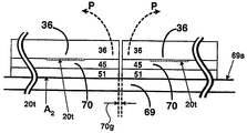
마찬가지로, 트랜스퍼 접착제 층(51)이 유연성 매체(45)와 접속되어 있을 것이므로, 유연성 매체(45)와 트랜스퍼 접착제 층(51)의 조합체가 유연성 매체(70)로서 표시될 것이다. 도 28 및 도 30에 있어서, 유연성 매체(70)와 광중합체 시임(36)의 조합체가 유연성 조립체(75)로서 표시될 것이다. 후술하는 바와 같이, 유연성 조립체(75)는 실린더 및 가요성 벨트 재료와 접속될 것이다.Similarly, since the transfer
도 31a 내지 도 31c에 있어서, 수평 섹션(73h) 및 수직 섹션(73v)을 포함하는 L자 형상의 지그(73)는 낮은 수직벽을 형성한다. 수평 및 수직 섹션(73h, 73v)은 서로 직각(β)을 이룬다. 섹션(73h, 73v)은 매끄럽고 실질적으로 편평해야 한다. L자 형상의 지그(73)는 유연성 조립체(75)의 적층을 실린더(69)의 표면(69s)에 이루는데 이용될 수 있다. 31A to 31C, the L-shaped
도 31a 및 도 31b에 있어서, 지지 기판(41)은 수평 섹션(73h)상에 위치되고, 수직 섹션(73v)에 대해 인접될 수 있다. 선택적으로, 유연성 조립체(75)가 지지 기판(41)으로부터 이미 분리된 경우, 매끈하고 편평한 피스의 실리콘 고무(도시하지 않음)로 이루어진 베드가 수평 섹션(73h)상에 위치될 수 있고, 베드의 단부는 수직 섹션(73v)에 대해 인접된다. 유연성 조립체(75)는 베드의 상부상에 위치되고, 수직 직선 에지로서 수직 섹션(73v)을 이용함으로써 수직 섹션(73v)과 정렬된다. 제 2 백킹(55)이 트랜스퍼 접착제 층(51)상에 여전히 있는 경우, 제 2 백킹(55)은 제 2 접착면(A2)을 노출시키기 위해 벗겨질 수 있다(P2).31A and 31B, the
도 31a 및 도 31c에 있어서, 외측면(69s)을 갖는 실린더(69)는 수평 섹션(73h) 및 수직 섹션(73v)과 정렬되어, 외측면(69s)은 이들 섹션(73h, 73v)에 접한다(73t). 실린더(69)는 제 2 접착 표면(A2)이 접점(73t)에서 외측 표면(69s)의 일부와 접촉하도록 유연성 조립체(75)상으로 낮춰진다. 그 다음, 실린더(69)는 롤 방향(RD)으로 롤링(R)되어 실린더(69)가 롤링(R)될 때 외측 표면(69s)상의 유연성 조립체(75)를 수집한다. 유연성 조립체(75)가 실린더(69)상에 롤링된 후에, 도 31b에 도시한 바와 같이 유연성 조립체(75)의 인접 단부 사이의 갭(70g)이 존재할 수 있다.31A and 31C, the
실린더(69)용으로 적합한 재료에는, 이에 제한되지는 않지만 금속, 세라믹, 유리, 석영 및 플라스틱이 포함된다. 바람직하게는, 실린더(69)는 광(L)이 실린더(69), 유연성 매체(70) 및 임프린트 스탬프(20t)를 통과할 수 있도록 선택적으로 투명한 재료로 이루어질 수 있다. 실린더(69)용으로 적합한 광학적으로 투명한 재료에는, 이에 제한되지는 않지만 유리, 석영 및 플라스틱이 포함된다. 도 32에 있어서, 자외선 광원과 같은 광원(99)은 실린더(69)의 내부 또는 외부에 위치설정되어 임프린트 스탬프(20t)와 접촉하도록 가압되는 광중합체 재료(도시하지 않음)를 조사하여 경화시킬 수 있다. 유연성 매체(70)가 임의의 크기로 이루어질 수 있기 때문에, 실린더(69)는 광원(99)을 수용하기에 적합한 내경을 포함할 수 있다. 한편, 광원(99)은 실린더(69)의 내경에 끼워맞춤하기에 충분히 작을 수 있다.Suitable materials for the
도 31b에 있어서, 유연성 매체(45)를 실린더(69)에 부착하기 위한 변형된 방법이 도시되어 있다. 유연성 매체는, 트랜스퍼 접착제 층(51)이 도 31b의 유연성 매체(45)와 접속하지 않기 때문에 참조부호(70) 대신에 참조부호(45)로 표시되어 있다. 우선, 트랜스퍼 접착제 층(51)의 제 1 접착 표면(A1)은 제 1 백킹(53)(도시하지 않음)을 다시 박리함으로써 노출된다. 둘째로, 실린더(69)의 외측 표면(69s)은 제 1 접착 표면(A1)과 연결되고, 그 다음 실린더(69)는 외측 표면(69s)상의 트랜스퍼 접착제 층(51)을 수집하도록 롤링된다. 셋째로, 제 2 백킹(55)의 일부는 제 2 접착 표면(A2)의 일부를 노출하도록 다시 박리된다. 다음에, 제 2 접착 표면(A2)의 노출 부분은 접점(73t)에서 유연성 매체(45)와 접속하고, 실린더(69)는 롤 방향(RD)으로 롤링되어 실린더(69)상의 유연성 매체(45)를 수집하는 동시에 제 2 접착 표면(A2)의 나머지 부분을 노출시키기 위해 제 2 백킹(55)의 나머지 부분을 다시 박리(55p)한다.In FIG. 31B, a modified method for attaching the flexible medium 45 to the
도 32 및 도 33에 있어서, 유연성 조립체(75)가 실린더(69)상에서 롤링된 후에, 유연성 조립체(75)의 주요부가 실린더(69)상에서 매끄럽게 롤링될 수 있도록 트리밍(tri㎜ing)되어야 하는 유연성 조립체(75)의 초과 부분(75x)이 존재할 수 있다. 상술한 바와 같이, 갭(70g)이 존재할 수 있고, 존재한다면 갭(70g)이 실용적일 수 있을 만큼 작도록 초과 부분(75x)을 트리밍하는 것이 바람직하다. 나이프(K) 등은 유연성 조립체(75)가 어떠한 볼록부 없이 외측 표면(69s)상에 놓이도록 초과 부분(75x)을 트리밍하는데 이용될 수 있다. 도 33에 있어서, 나이프(K)는 방향(Kd)을 따라 절단하여 완전히 적층된 실린더(90)를 형성하는 초과 부분(75x)의 트리밍을 수행할 수 있다. 도 33에 있어서, 임프린트 스탬프(20t)는 유연성 매체(70)으로부터 분리되지 않았던 광중합체 시임(36) 아래에 여전히 위치설정되어 있기 때문에 점선으로 도시되어 있다.32 and 33, after the
도 33에 있어서, 실린더(69) 및 유연성 조립체(75)를 통과하는 n-n선은 도 34a 및 도 34b에서 단면도로 보다 상세하게 도시되어 있다. 도 34a에 있어서, 유연성 조립체(75)는 초과 부분(75x)의 트리밍 이전 상태가 도시되어 있다. 도 34b에 있어서, 유연성 조립체(75)는 초과 부분(75x)의 트리밍 후 상태가 도시되어 있다.In FIG. 33, the n-n line through the
도 34a에 있어서, 초과 부분(75x)은 유연성 매체(70) 및 광중합체 시임(36)을 포함한다. 광중합체 시임(36)과 접속된 얇은 플라스틱 필름(33)(도 28 참조)은 광에 불투명하고 광중합체 시임(36)이 광학적으로 투명할 수 있기 때문에, 광중합체 시임(36)은 점선 화살표(P)로 표시된 바와 같이 다시 박리될 수 있어서, 유연성 매체(70)[즉, 광학적으로 투명한 접착제(51) 및 광학적으로 투명한 유연성 매체(45)]가 실린더(69)의 외측 표면(69s)과 이미 접속하고 있는 유연성 조립체(75)의 에지(Es)를 따라 볼 수 있게 이용될 수 있다.In FIG. 34A,
에지(Es)에 대한 조준선(sight line)(점선 참조)을 따른 나이프(K)는 초과 부분(75x)을 잘라내는데 이용되어 초과 부분(75x)의 비접속층이 그들 각각의 접촉층, 즉 도 34a에 도시한 바와 같은 참조부호(36' 내지 36; 45' 내지 45; 및 51' 내지 51)와 정렬될 것이다. 트리밍 후에, 유연성 조립체(75)의 인접 단부 사이의 작은 갭(70g)이 존재할 수 있다.The knife K along the sight line (see dashed line) to the edge E s is used to cut off the
도 34b에 있어서, 갭(70g)이 없는 경우, 유연성 조립체(75)는 실린더(69)의 외측 표면(69s)상에 거의 연속적인 층을 형성한다. 트리밍 후에, 광중합체 시임(36)은 유연성 매체(70)상의 임프린트 스탬프(20t)를 노출하도록 다시 박리(P)될 수 있다.In FIG. 34B, in the absence of a
도 35 및 도 36에 있어서, 유연성 조립체(75)는 벨트 재료(81)에 적용된다. 유연성 조립체(75)를 벨트 재료(81)에 적용하기 전에, 제 2 백킹(55)은 제 2 접착 표면(A2)을 노출하도록 트랜스퍼 접착제 층(51)으로부터 박리된다. 그 다음, 제 2 접착 표면(A2)은 벨트 재료(81)의 표면(81s)에 점진적으로 적용된다. 고무 롤러와 같은 롤러(89)는 롤 방향(RD)으로 유연성 조립체(75)를 롤링(R)하는데 이용될 수 있다.35 and 36, the
롤링(R)은 유연성 조립체(75) 및 벨트 재료(81)의 제 1 단부(75a, 81a)에서 시작되어, 제 2 단부(75b, 81b)에서 종결될 수 있다. 유연성 조립체(75) 및 벨트 재료(81)가 서로 접속된 후(도 36 참조)에, 제 1 및 제 2 단부(81a, 81b)는 도 37a 및 도 37b에 도시한 바와 같이 벨트(100)를 형성하도록 결합될 수 있다. 상술한 바와 같이, 갭(70g)은 제 1 및 제 2 단부(75a, 75b)를 분리할 수 있다. 접합 테이프(splicing tape) 등은 갭(70g)을 덮는데 이용될 수 있다. 또한, 한 장의 접합 테이프(81t) 등은 벨트(100)를 형성하기 위한 벨트 재료(81)의 제 1 및 제 2 단부(81a, 81b)를 접속하는데 이용될 수도 있다. 벨트(100)가 형성된 후에, 층(71)[즉, 참조부호(33, 36)]은 유연성 매체(70)상의 임프린트 스탬프(20t)를 노출하도록 다시 박리(P)될 수 있다. 적당한 접합 테이프에는, 이에 제한되지는 않지만 고온 실리콘계 테이프가 포함된다.Rolling R may begin at the first ends 75a and 81a of the
벨트 재료(81)는 광(L)이 벨트 재료(81), 유연성 매체(70) 및 임프린트 스탬프(20t)를 통과할 수 있도록 광학적으로 투명한 재료일 수 있다. 벨트 재료(81)용으로 적당한 광학적으로 투명한 재료에는, 이에 제한되지는 않지만 듀퐁(등록상표) 마일라(등록상표)가 포함된다. 예를 들면, 자외선 광원과 같은 광원(99)은 벨트(100)의 내부 또는 외부에 위치설정되어 임프린트 스탬프(20t)와 접촉하게 가압되는 광중합체 재료(도시하지 않음)를 조사하여 경화할 수 있다. 벨트 재료(81)는 약 50.0㎛ 내지 약 150.0㎛의 두께(tB)를 가질 수 있다.
본 발명의 장치 및 방법의 몇 가지 실시예가 본원에서 개시되고 기술되었지만, 본 발명은 상기에서 기술되고 도시된 구성요소의 특정 형태 또는 구성에 제한되지는 않는다. 본 발명은 특허청구범위에 의해서만 제한된다.
While several embodiments of the apparatus and method of the present invention have been disclosed and described herein, the invention is not limited to the specific form or configuration of components described and illustrated above. The invention is limited only by the claims.
본 발명에 따른 임프린트 패턴을 갖는 광중합체 코팅식 가요성 기판을 엠보싱 가공하기 위한 장치를 이용하면, 임프린트 스탬프가 엠보싱 가공과 동시에 자외선이 유연성 매체를 통해 조사되어, 전사된 임프린트 패턴을 경화하고, 그 형상을 유지할 수 있다.Using an apparatus for embossing a photopolymer-coated flexible substrate having an imprint pattern according to the present invention, the imprint stamp is irradiated with ultraviolet light through a flexible medium at the same time as the embossing process to cure the transferred imprint pattern, and The shape can be maintained.
Claims (32)
Applications Claiming Priority (2)
| Application Number | Priority Date | Filing Date | Title |
|---|---|---|---|
| US10/425,798 | 2003-04-29 | ||
| US10/425,798 US7070406B2 (en) | 2003-04-29 | 2003-04-29 | Apparatus for embossing a flexible substrate with a pattern carried by an optically transparent compliant media |
Publications (2)
| Publication Number | Publication Date |
|---|---|
| KR20040093460A KR20040093460A (en) | 2004-11-05 |
| KR101060355B1 true KR101060355B1 (en) | 2011-08-29 |
Family
ID=32990380
Family Applications (1)
| Application Number | Title | Priority Date | Filing Date |
|---|---|---|---|
| KR1020040029554A Expired - Fee Related KR101060355B1 (en) | 2003-04-29 | 2004-04-28 | Embossing processing equipment |
Country Status (6)
| Country | Link |
|---|---|
| US (2) | US7070406B2 (en) |
| EP (1) | EP1473594A3 (en) |
| JP (1) | JP2004322641A (en) |
| KR (1) | KR101060355B1 (en) |
| CN (1) | CN1541852A (en) |
| TW (1) | TWI240150B (en) |
Families Citing this family (125)
| Publication number | Priority date | Publication date | Assignee | Title |
|---|---|---|---|---|
| US7066234B2 (en) | 2001-04-25 | 2006-06-27 | Alcove Surfaces Gmbh | Stamping tool, casting mold and methods for structuring a surface of a work piece |
| CN1262883C (en) | 2000-07-17 | 2006-07-05 | 得克萨斯州大学系统董事会 | Method and system of automatic fluid dispensing for imprint lithography processes |
| WO2002067055A2 (en) * | 2000-10-12 | 2002-08-29 | Board Of Regents, The University Of Texas System | Template for room temperature, low pressure micro- and nano-imprint lithography |
| US20050064344A1 (en) * | 2003-09-18 | 2005-03-24 | University Of Texas System Board Of Regents | Imprint lithography templates having alignment marks |
| US20080160129A1 (en) | 2006-05-11 | 2008-07-03 | Molecular Imprints, Inc. | Template Having a Varying Thickness to Facilitate Expelling a Gas Positioned Between a Substrate and the Template |
| US7179079B2 (en) * | 2002-07-08 | 2007-02-20 | Molecular Imprints, Inc. | Conforming template for patterning liquids disposed on substrates |
| US7070406B2 (en) * | 2003-04-29 | 2006-07-04 | Hewlett-Packard Development Company, L.P. | Apparatus for embossing a flexible substrate with a pattern carried by an optically transparent compliant media |
| US7804649B2 (en) | 2003-09-09 | 2010-09-28 | 3M Innovative Properties Company | Microreplicated achromatic lens |
| ATE551383T1 (en) | 2003-09-23 | 2012-04-15 | Univ North Carolina | PHOTOHARDENABLE PERFLUORUM POLYETHERS FOR USE AS NEW MATERIALS IN MICROFLUIDIC DEVICES |
| US7314365B2 (en) * | 2003-09-24 | 2008-01-01 | Fuji Photo Film Co., Ltd. | Surface treating apparatus and image recording apparatus |
| US9040090B2 (en) * | 2003-12-19 | 2015-05-26 | The University Of North Carolina At Chapel Hill | Isolated and fixed micro and nano structures and methods thereof |
| KR101376715B1 (en) | 2003-12-19 | 2014-03-27 | 더 유니버시티 오브 노쓰 캐롤라이나 엣 채플 힐 | Methods for fabricating isolated micro- and nano- structures using soft or imprint lithography |
| US8535041B2 (en) * | 2006-07-28 | 2013-09-17 | Microcontinuum, Inc. | Addressable flexible patterns |
| US9307648B2 (en) | 2004-01-21 | 2016-04-05 | Microcontinuum, Inc. | Roll-to-roll patterning of transparent and metallic layers |
| CA2555912A1 (en) * | 2004-02-13 | 2005-09-15 | The University Of North Carolina At Chapel Hill | Functional materials and novel methods for the fabrication of microfluidic devices |
| US20060115999A1 (en) | 2004-12-01 | 2006-06-01 | Molecular Imprints, Inc. | Methods of exposure for the purpose of thermal management for imprint lithography processes |
| US7730834B2 (en) * | 2004-03-04 | 2010-06-08 | Asml Netherlands B.V. | Printing apparatus and device manufacturing method |
| US7140861B2 (en) | 2004-04-27 | 2006-11-28 | Molecular Imprints, Inc. | Compliant hard template for UV imprinting |
| US7785526B2 (en) * | 2004-07-20 | 2010-08-31 | Molecular Imprints, Inc. | Imprint alignment method, system, and template |
| US7309225B2 (en) | 2004-08-13 | 2007-12-18 | Molecular Imprints, Inc. | Moat system for an imprint lithography template |
| WO2006059580A1 (en) * | 2004-11-30 | 2006-06-08 | Asahi Glass Company, Limited | Mold and process for production of substrates having transferred micropatterns thereon |
| US7125495B2 (en) | 2004-12-20 | 2006-10-24 | Palo Alto Research Center, Inc. | Large area electronic device with high and low resolution patterned film features |
| US20060177535A1 (en) * | 2005-02-04 | 2006-08-10 | Molecular Imprints, Inc. | Imprint lithography template to facilitate control of liquid movement |
| CN101156107B (en) * | 2005-02-03 | 2010-11-24 | 北卡罗来纳大学查珀尔希尔分校 | Low Surface Energy Polymer Materials for Liquid Crystal Displays |
| US20060182838A1 (en) * | 2005-02-11 | 2006-08-17 | Park Hyung K | Apparatus and method for vacuum forming a film |
| TWI261308B (en) * | 2005-03-02 | 2006-09-01 | Ind Tech Res Inst | Micro-nanometer transfer printer |
| EP1871584B1 (en) | 2005-03-09 | 2009-11-18 | 3M Innovative Properties Company | Apparatus and method for producing two-sided patterned web in registration |
| BRPI0608696A2 (en) | 2005-03-09 | 2010-12-07 | 3M Innovative Properties Co | roll to roll microreplication apparatus and method of producing a microreplicated article |
| TWI271777B (en) * | 2005-04-27 | 2007-01-21 | Ind Tech Res Inst | Uniform pressing micro-nano transfer printing apparatus |
| KR100616728B1 (en) * | 2005-07-07 | 2006-08-28 | 드림칼라(주) | Scratch Stamping Device on Film Surface and Manufacturing Method Thereof |
| US20090304992A1 (en) * | 2005-08-08 | 2009-12-10 | Desimone Joseph M | Micro and Nano-Structure Metrology |
| EP1922364A4 (en) | 2005-08-09 | 2010-04-21 | Univ North Carolina | METHODS AND MATERIALS FOR MANUFACTURING MICROFLUIDIC DEVICES |
| US8191500B2 (en) * | 2005-11-24 | 2012-06-05 | Kronoplus Technical Ag | Coating device comprising flowing coating material for smooth or structured surfaces |
| US9174400B2 (en) | 2006-02-15 | 2015-11-03 | Osram Opto Semiconductors Gmbh | Method for producing structures in optoelectronic components and device for this purpose |
| DE102006024423A1 (en) * | 2006-02-15 | 2007-08-16 | Osram Opto Semiconductors Gmbh | Structure producing method for multiple opto-electronic components, involves producing pressure between roller and auxiliary carrier by relative movement of roller relatively to auxiliary carrier |
| US20070204953A1 (en) * | 2006-02-21 | 2007-09-06 | Ching-Bin Lin | Method for forming structured film as molded by tape die |
| CA2643510C (en) | 2006-02-27 | 2014-04-29 | Microcontinuum, Inc. | Formation of pattern replicating tools |
| US20070216050A1 (en) * | 2006-03-17 | 2007-09-20 | Kim Sang M | Optical member fabricating apparatus and method and forming mold used for the same |
| US20070218255A1 (en) * | 2006-03-20 | 2007-09-20 | Gray Lorin S Iii | Films for decorating glass and methods of their production |
| WO2007117524A2 (en) | 2006-04-03 | 2007-10-18 | Molecular Imprints, Inc. | Method of concurrently patterning a substrate having a plurality of fields and alignment marks |
| US8287266B2 (en) * | 2006-06-16 | 2012-10-16 | GKN Aerospace Services Structures, Corp. | Device for performing consolidation and method of use thereof |
| WO2008011051A1 (en) * | 2006-07-17 | 2008-01-24 | Liquidia Technologies, Inc. | Nanoparticle fabrication methods, systems, and materials |
| KR100783859B1 (en) | 2006-07-28 | 2007-12-10 | 정동희 | Pad Molding Device |
| US20080079183A1 (en) * | 2006-09-28 | 2008-04-03 | Chi Lin Technology Co., Ltd. | Method for making an optical element |
| KR20090079946A (en) | 2006-11-15 | 2009-07-22 | 쓰리엠 이노베이티브 프로퍼티즈 컴파니 | Flexographic printing to cure during transfer to substrate |
| US8128393B2 (en) * | 2006-12-04 | 2012-03-06 | Liquidia Technologies, Inc. | Methods and materials for fabricating laminate nanomolds and nanoparticles therefrom |
| KR100964985B1 (en) | 2006-12-14 | 2010-06-21 | 미래나노텍(주) | Manufacturing apparatus of optical sheet and its manufacturing method |
| US20080271625A1 (en) * | 2007-01-22 | 2008-11-06 | Nano Terra Inc. | High-Throughput Apparatus for Patterning Flexible Substrates and Method of Using the Same |
| US20080176049A1 (en) * | 2007-01-24 | 2008-07-24 | Samsung Electronics Co., Ltd. | PHOTO-CURABLE COMPOSITION HAVING INHERENTLY EXCELLENT RELEASING PROPERtY AND PATTERN TRANSFER PROPERTY, METHOD FOR TRANSFERRING PATTERN USING THE COMPOSITION AND LIGHT RECORDING MEDIUM HAVING POLYMER PATTERN LAYER PRODUCED USING THE COMPOSITION |
| JP2008194977A (en) * | 2007-02-14 | 2008-08-28 | Hitachi Maxell Ltd | Manufacturing method and manufacturing apparatus of molded body |
| KR100804734B1 (en) * | 2007-02-22 | 2008-02-19 | 연세대학교 산학협력단 | Continuous Lithography Apparatus and Method Using UV Roll Nanoimprinting |
| US8940117B2 (en) | 2007-02-27 | 2015-01-27 | Microcontinuum, Inc. | Methods and systems for forming flexible multilayer structures |
| US20080229941A1 (en) | 2007-03-19 | 2008-09-25 | Babak Heidari | Nano-imprinting apparatus and method |
| WO2008118861A2 (en) * | 2007-03-23 | 2008-10-02 | The University Of North Carolina At Chapel Hill | Discrete size and shape specific organic nanoparticles designed to elicit an immune response |
| KR20080088238A (en) * | 2007-03-29 | 2008-10-02 | 삼성전자주식회사 | Pattern forming mold, pattern forming apparatus and pattern forming method |
| US7964243B2 (en) * | 2007-04-30 | 2011-06-21 | S.D. Warren Company | Materials having a textured surface and methods for producing same |
| PL2164703T3 (en) | 2007-06-28 | 2019-03-29 | Emot Co., Ltd | Method of duplicating nano-scaled pattern texture on object's surface by imprinting and electroforming |
| KR100894736B1 (en) * | 2007-08-22 | 2009-04-24 | 한국기계연구원 | Large area imprint apparatus capable of roll pressurization and continuous resin coating |
| WO2009032815A1 (en) * | 2007-09-06 | 2009-03-12 | 3M Innovative Properties Company | Tool for making microstructured articles |
| ATE534500T1 (en) * | 2007-09-06 | 2011-12-15 | 3M Innovative Properties Co | METHOD FOR SHAPING MOLDING TOOLS AND METHOD FOR SHAPING ARTICLES USING THE MOLDING TOOLS |
| CN101796443A (en) | 2007-09-06 | 2010-08-04 | 3M创新有限公司 | Lightguides having light extraction structures providing regional control of light output |
| EP2208100B8 (en) | 2007-10-11 | 2017-08-16 | 3M Innovative Properties Company | Chromatic confocal sensor |
| US9472699B2 (en) | 2007-11-13 | 2016-10-18 | Battelle Energy Alliance, Llc | Energy harvesting devices, systems, and related methods |
| US7792644B2 (en) | 2007-11-13 | 2010-09-07 | Battelle Energy Alliance, Llc | Methods, computer readable media, and graphical user interfaces for analysis of frequency selective surfaces |
| US8071931B2 (en) | 2007-11-13 | 2011-12-06 | Battelle Energy Alliance, Llc | Structures, systems and methods for harvesting energy from electromagnetic radiation |
| CN101946305B (en) | 2007-12-12 | 2014-02-12 | 3M创新有限公司 | Method for making structures with improved edge definition |
| TW200932504A (en) * | 2008-01-18 | 2009-08-01 | Univ Nat Taiwan | An improved roller embossing apparatus |
| US20120282554A1 (en) * | 2008-01-22 | 2012-11-08 | Rolith, Inc. | Large area nanopatterning method and apparatus |
| US8518633B2 (en) * | 2008-01-22 | 2013-08-27 | Rolith Inc. | Large area nanopatterning method and apparatus |
| KR101268961B1 (en) * | 2008-02-22 | 2013-05-29 | 엘지디스플레이 주식회사 | Fabricating method of light guiding plate and backlight unit with the same |
| US8605256B2 (en) * | 2008-02-26 | 2013-12-10 | 3M Innovative Properties Company | Multi-photon exposure system |
| EP2246177B1 (en) * | 2008-02-27 | 2018-06-06 | Sharp Kabushiki Kaisha | Roller type nano-imprint device, mold roll for the roller type nano-imprint device, fixed roll for the roller type nano-imprint device, and nano-imprint sheet manufacturing method |
| US8597767B2 (en) | 2008-03-04 | 2013-12-03 | Sharp Kabushiki Kaisha | Optical element, roller type nanoimprinting apparatus, and process for producing die roll |
| WO2009151171A1 (en) * | 2008-06-13 | 2009-12-17 | Miraenanotech Co., Ltd. | Apparatus and method for manufacturing an optical sheet |
| US8021935B2 (en) | 2008-10-01 | 2011-09-20 | Hewlett-Packard Development Company, L.P. | Thin film device fabrication process using 3D template |
| KR101512876B1 (en) * | 2008-08-27 | 2015-04-16 | 에이엠오 게엠베하 | Improved nanoimprint method |
| TW201022017A (en) * | 2008-09-30 | 2010-06-16 | Molecular Imprints Inc | Particle mitigation for imprint lithography |
| US20110210480A1 (en) * | 2008-11-18 | 2011-09-01 | Rolith, Inc | Nanostructures with anti-counterefeiting features and methods of fabricating the same |
| KR20100068830A (en) * | 2008-12-15 | 2010-06-24 | 삼성전자주식회사 | Imprint mold, imprint apparatus and method of manucacturing pattern |
| CN101833237B (en) * | 2009-03-13 | 2013-01-09 | 鸿富锦精密工业(深圳)有限公司 | Pressing device |
| CN101900935B (en) * | 2009-05-27 | 2012-09-05 | 比亚迪股份有限公司 | Ultraviolet impressing method and device thereof |
| US8551386B2 (en) | 2009-08-03 | 2013-10-08 | S.D. Warren Company | Imparting texture to cured powder coatings |
| EP2467755B1 (en) * | 2009-08-21 | 2016-10-12 | Basf Se | Method for a sub microscopic and optically variable image carrying device |
| KR100957622B1 (en) * | 2009-09-07 | 2010-05-13 | 한국기계연구원 | Printing apparatus using thermal roll imprinting and patterned plate and films laminating apparatus for microfluidics and sensor and printing method using the same |
| KR101549267B1 (en) * | 2009-10-14 | 2015-09-11 | 엘지디스플레이 주식회사 | Method for manufacturing thin film transistor array substrate |
| KR101568268B1 (en) * | 2009-10-27 | 2015-11-11 | 엘지디스플레이 주식회사 | Thin film transistor substrate and method of fabricating the same |
| RU2438872C2 (en) * | 2010-01-11 | 2012-01-10 | Государственное образовательное учреждение высшего профессионального образования "Тихоокеанский государственный университет" | Device for processing plastic articles |
| US9465296B2 (en) * | 2010-01-12 | 2016-10-11 | Rolith, Inc. | Nanopatterning method and apparatus |
| US8691134B2 (en) | 2010-01-28 | 2014-04-08 | Molecular Imprints, Inc. | Roll-to-roll imprint lithography and purging system |
| TW201125735A (en) * | 2010-01-29 | 2011-08-01 | Hon Hai Prec Ind Co Ltd | Roller device |
| JP5693019B2 (en) * | 2010-03-01 | 2015-04-01 | ユニ・チャーム株式会社 | Rotating machine |
| US20110229695A1 (en) * | 2010-03-18 | 2011-09-22 | Stanley Michael Marcinkowski | Articles having metalizing and holographic effects |
| TW201202008A (en) * | 2010-07-12 | 2012-01-16 | Hon Hai Prec Ind Co Ltd | Device and method for making optical film |
| TW201208857A (en) * | 2010-08-16 | 2012-03-01 | Hon Hai Prec Ind Co Ltd | Film manufacturing device |
| CN103097953A (en) * | 2010-08-23 | 2013-05-08 | 罗利诗公司 | Mask for near-field lithography and fabrication the same |
| KR20120030317A (en) * | 2010-09-17 | 2012-03-28 | 소니 주식회사 | Manufacturing method of laminated body, stamper, transfer device, laminated body, molding element, and optical element |
| TW201219193A (en) * | 2010-11-02 | 2012-05-16 | Ind Tech Res Inst | Uniform pressing apparatus for roll-to-sheet |
| WO2012157636A1 (en) * | 2011-05-19 | 2012-11-22 | 綜研化学株式会社 | Nanoimprint mold and curved body |
| WO2013059078A1 (en) | 2011-10-19 | 2013-04-25 | Unipixel Displays, Inc. | Photo-patterning using a translucent cylindrical master to form microscopic conductive lines on a flexible substrate |
| TW201334948A (en) * | 2012-02-21 | 2013-09-01 | Coretronic Corp | Imprinting apparatus and imprinting method |
| US9616614B2 (en) * | 2012-02-22 | 2017-04-11 | Canon Nanotechnologies, Inc. | Large area imprint lithography |
| US8847824B2 (en) | 2012-03-21 | 2014-09-30 | Battelle Energy Alliance, Llc | Apparatuses and method for converting electromagnetic radiation to direct current |
| US9233511B2 (en) * | 2012-05-10 | 2016-01-12 | Optiz, Inc. | Method of making stamped multi-layer polymer lens |
| US20150140309A1 (en) * | 2012-05-11 | 2015-05-21 | 10X Technology Llc | Process and Apparatus for Embossing Precise Microstructures in Rigid Thermoplastic Panels |
| DE102012112556B4 (en) * | 2012-12-18 | 2018-09-27 | Isimat Gmbh Siebdruckmaschinen | Method and apparatus for cold stamping on three-dimensional objects |
| KR101303194B1 (en) * | 2013-04-24 | 2013-09-03 | 한국기계연구원 | Liquid transfer imprint lithography apparatus using a roll stamp and the method |
| US9589797B2 (en) | 2013-05-17 | 2017-03-07 | Microcontinuum, Inc. | Tools and methods for producing nanoantenna electronic devices |
| DE202014104613U1 (en) | 2014-04-09 | 2015-08-11 | Kuka Systems Gmbh | applicator |
| CN104943430A (en) * | 2015-05-26 | 2015-09-30 | 深圳市中联讯科技有限公司 | UV transferring method for transparent plate |
| TWI556942B (en) * | 2015-07-23 | 2016-11-11 | Aurotek Corp | Roller imprinting system |
| TWI584938B (en) * | 2015-07-23 | 2017-06-01 | Aurotek Corp | Roller imprinting system |
| KR102655948B1 (en) | 2015-12-29 | 2024-04-09 | 쓰리엠 이노베이티브 프로퍼티즈 캄파니 | Additive manufacturing methods for adhesives and adhesive articles |
| EP3397445B1 (en) * | 2015-12-29 | 2021-07-14 | 3M Innovative Properties Company | Continuous additive manufacturing apparatus |
| US11597856B2 (en) | 2015-12-29 | 2023-03-07 | 3M Innovative Properties Company | Continuous additive manufacturing methods |
| JP6741440B2 (en) * | 2016-02-29 | 2020-08-19 | 住友化学株式会社 | Laminated optical film manufacturing method and laminated optical film manufacturing apparatus |
| DK3455676T3 (en) * | 2016-07-14 | 2019-12-09 | Morphotonics Holding Bv | DEVICE FOR PRINTING DISCRETE SUBSTRATES WITH A DISCREET FLEXIBLE STAMP |
| NZ754245A (en) * | 2016-12-22 | 2025-07-25 | Illumina Inc | Imprinting apparatus |
| US20180297267A1 (en) * | 2017-04-11 | 2018-10-18 | Carpe Diem Technologies, Inc. | System and method of manufacturing a cylindrical nanoimprint lithography master |
| KR101843548B1 (en) | 2017-12-12 | 2018-03-30 | 주식회사 에이디피 | A method for manufacturing glass sunting film having complex pattern |
| CN109116678A (en) * | 2018-08-21 | 2019-01-01 | 中国科学院深圳先进技术研究院 | Roll ultraviolet nanometer imprinting apparatus |
| KR102666843B1 (en) * | 2018-08-31 | 2024-05-21 | 삼성디스플레이 주식회사 | Master stamp for nano imprint and method of manufacturing of the smae |
| US11104075B2 (en) | 2018-11-01 | 2021-08-31 | Stratasys, Inc. | System for window separation in an additive manufacturing process |
| WO2020093028A1 (en) | 2018-11-01 | 2020-05-07 | Origin Laboratories, Inc. | Method for build separation from a curing interface in an additive manufacturing process |
| US11408589B2 (en) | 2019-12-05 | 2022-08-09 | Optiz, Inc. | Monolithic multi-focus light source device |
| US20220305715A1 (en) * | 2020-09-08 | 2022-09-29 | Prntsys Makina Ve Ambalaj Sanayi Ticaret Limited Sirketi | A micro embossing unit with a belt system |
Citations (4)
| Publication number | Priority date | Publication date | Assignee | Title |
|---|---|---|---|---|
| JPH1016048A (en) * | 1996-06-27 | 1998-01-20 | Idemitsu Petrochem Co Ltd | Method and equipment for processing embossed pattern and embossed-surface-shaped thermoplastic resin |
| JPH11147059A (en) * | 1997-08-04 | 1999-06-02 | Hsm Holographic Syst Muenchen Gmbh | Method and apparatus for producing a surface structure, particularly a hologram surface structure, on a substrate |
| KR100425511B1 (en) | 2000-08-23 | 2004-03-30 | 양근창 | Apparatus and Method for Manufacturing light guide plate for plane light source unit |
| KR100454801B1 (en) | 1996-06-26 | 2005-01-17 | 이데미쓰세끼유가가꾸가부시끼가이샤 | Method of emboss pattern process, emboss pattern processing apparatus, and embossed sheet |
Family Cites Families (51)
| Publication number | Priority date | Publication date | Assignee | Title |
|---|---|---|---|---|
| US2516254A (en) * | 1947-06-06 | 1950-07-25 | Johns Manville | Method of embossing structural panels |
| US2849752A (en) * | 1956-12-17 | 1958-09-02 | Ibm | Machine for embossing thermoplastic workpiece |
| DE1164643B (en) * | 1962-03-02 | 1964-03-05 | Dornbusch & Co | Method and device for hot stamping webs of material, in particular thermoplastic plastic films |
| US3345234A (en) * | 1963-03-21 | 1967-10-03 | Congoleum Nairn Inc | Continuous method for making decorative floor covering |
| US3888283A (en) * | 1971-12-27 | 1975-06-10 | Ford B Cauffiel | Tapered pole made of variable width metal strips |
| US3757042A (en) * | 1972-02-18 | 1973-09-04 | Us Navy | Receiver separation and zoom lenses pan and tilt underwater optical viewing system with adjustable source |
| US4038917A (en) * | 1972-07-18 | 1977-08-02 | Westvaco Corporation | Thin belt embossing method and apparatus |
| FR2318742A1 (en) * | 1975-07-21 | 1977-02-18 | Rejto Thomas | TRANSFER PRINTING PROCESS WITH SIMULTANEOUS EMBOSSING AND INSTALLATION FOR IMPLEMENTING THE PROCESS |
| US4341581A (en) * | 1978-03-30 | 1982-07-27 | Inmont Corporation | Method of making leatherlike materials (B) |
| US4248652A (en) * | 1978-03-30 | 1981-02-03 | Inmont Corporation | Method of making leatherlike materials (A) |
| DE3376685D1 (en) * | 1982-12-21 | 1988-06-23 | Ares Serono Nv | Assay technique |
| GB8423204D0 (en) * | 1984-09-14 | 1984-10-17 | Comtech Res Unit | Assay technique and equipment |
| JPS6259954A (en) * | 1985-09-10 | 1987-03-16 | Fuji Photo Film Co Ltd | Manufacture of protective coating layer for photographic element |
| US4769202A (en) * | 1985-11-29 | 1988-09-06 | The B. F. Goodrich Company | Process of making a conveyor belt |
| GB8618133D0 (en) * | 1986-07-24 | 1986-09-03 | Pa Consulting Services | Biosensors |
| US4943351A (en) * | 1988-05-23 | 1990-07-24 | Beloit Corporation | Transfer apparatus and method |
| US5049918A (en) * | 1988-08-25 | 1991-09-17 | Brother Kogyo Kabushiki Kaisha | Color image recording apparatus |
| US5230776A (en) * | 1988-10-25 | 1993-07-27 | Valmet Paper Machinery, Inc. | Paper machine for manufacturing a soft crepe paper web |
| WO1990015673A1 (en) * | 1989-06-12 | 1990-12-27 | General Electric Company | A laminar impressor for coating flat substrates |
| US5118532A (en) * | 1990-02-27 | 1992-06-02 | Vytech Industries, Inc. | Method of producing decorative vertical louver window covering material and decorative vertical louver material so produced |
| JPH03266237A (en) * | 1990-03-15 | 1991-11-27 | Canon Inc | Production of substrate for optical recording medium |
| US5103256A (en) * | 1990-04-12 | 1992-04-07 | Brother Kogyo Kabushiki Kaisha | Image forming apparatus using mask original form |
| US5031080A (en) * | 1990-05-24 | 1991-07-09 | Gulton Industries, Inc. | Portable cockpit light assembly |
| JP2883436B2 (en) * | 1990-10-18 | 1999-04-19 | 大日本印刷株式会社 | Hologram duplication method and apparatus |
| DE4035873A1 (en) * | 1990-11-12 | 1992-05-14 | Hoechst Ag | DEVICE AND METHOD FOR PRODUCING A MULTILAYER FILM COMPOSITE |
| DE4136679A1 (en) * | 1991-11-07 | 1993-05-13 | Hoechst Ag | DEVICE AND METHOD FOR PRODUCING A MULTILAYER FILM COMPOSITE |
| US5327225A (en) * | 1993-01-28 | 1994-07-05 | The Center For Innovative Technology | Surface plasmon resonance sensor |
| GB9320326D0 (en) | 1993-10-01 | 1993-11-17 | Ici Plc | Organic optical components and preparation thereof |
| US5460757A (en) * | 1993-12-29 | 1995-10-24 | Topstamp, Inc. | Method for manufacturing pre-inked stamps |
| US6206672B1 (en) * | 1994-03-31 | 2001-03-27 | Edward P. Grenda | Apparatus of fabricating 3 dimensional objects by means of electrophotography, ionography or a similar process |
| US5780140A (en) * | 1996-09-23 | 1998-07-14 | Reflexite Corporation | Retroreflective microprismatic material with top face curvature and method of making same |
| GB9509487D0 (en) | 1995-05-10 | 1995-07-05 | Ici Plc | Micro relief element & preparation thereof |
| US5633724A (en) * | 1995-08-29 | 1997-05-27 | Hewlett-Packard Company | Evanescent scanning of biochemical array |
| AU7598996A (en) * | 1995-10-25 | 1997-05-15 | University Of Washington | Surface plasmon resonance probe systems based on a folded planar lightpipe |
| US5917607A (en) * | 1996-04-25 | 1999-06-29 | Fuji Photo Film Co., Ltd. | Surface plasmon sensor for multiple channel analysis |
| GB9623185D0 (en) | 1996-11-09 | 1997-01-08 | Epigem Limited | Improved micro relief element and preparation thereof |
| DE19721170A1 (en) * | 1997-05-21 | 1998-11-26 | Emtec Magnetics Gmbh | Method and device for producing a film or a layer with a surface structure on both sides |
| US6018383A (en) * | 1997-08-20 | 2000-01-25 | Anvik Corporation | Very large area patterning system for flexible substrates |
| US6024907A (en) * | 1998-02-02 | 2000-02-15 | Bruce Jagunich | Embossing with an endless belt composed of a shape memory alloy |
| US6149849A (en) * | 1998-08-14 | 2000-11-21 | The Procter & Gamble Copmany | Process and apparatus for making papermaking belt |
| US6200399B1 (en) * | 1999-01-14 | 2001-03-13 | Avery Dennison Corporation | Method and apparatus for embossing a precision pattern of micro-prismatic elements in a resinous sheet or laminate |
| US6517995B1 (en) | 1999-09-14 | 2003-02-11 | Massachusetts Institute Of Technology | Fabrication of finely featured devices by liquid embossing |
| US6908295B2 (en) * | 2000-06-16 | 2005-06-21 | Avery Dennison Corporation | Process and apparatus for embossing precise microstructures and embossing tool for making same |
| US6456816B1 (en) * | 2000-10-04 | 2002-09-24 | Nexpress Solutions Llc | Method and apparatus for an intermediate image transfer member |
| US20030006535A1 (en) * | 2001-06-26 | 2003-01-09 | Michael Hennessey | Method and apparatus for forming microstructures on polymeric substrates |
| US6866737B2 (en) * | 2001-09-18 | 2005-03-15 | Awi Licensing Company | Method for mechanically embossing a surface covering using a recyclable solidified slurry embossing tool |
| JP3580280B2 (en) * | 2001-10-25 | 2004-10-20 | 株式会社日立製作所 | Recording medium and manufacturing method thereof |
| DE10157451A1 (en) * | 2001-11-23 | 2003-06-05 | Voith Paper Patent Gmbh | Method and device for producing a fibrous web |
| US20050167890A1 (en) * | 2002-06-26 | 2005-08-04 | Energy Conversion Devices, Inc. | Method and apparatus for forming microstructures on polymeric substrates |
| EP1583657A1 (en) * | 2003-01-06 | 2005-10-12 | Avery Dennison Corporation | Embossed oriented optical films |
| US7070406B2 (en) * | 2003-04-29 | 2006-07-04 | Hewlett-Packard Development Company, L.P. | Apparatus for embossing a flexible substrate with a pattern carried by an optically transparent compliant media |
-
2003
- 2003-04-29 US US10/425,798 patent/US7070406B2/en not_active Expired - Lifetime
- 2003-11-26 EP EP03027323A patent/EP1473594A3/en not_active Withdrawn
- 2003-11-28 TW TW092133541A patent/TWI240150B/en not_active IP Right Cessation
-
2004
- 2004-03-01 CN CNA200410007348XA patent/CN1541852A/en active Pending
- 2004-04-22 JP JP2004127052A patent/JP2004322641A/en not_active Withdrawn
- 2004-04-28 KR KR1020040029554A patent/KR101060355B1/en not_active Expired - Fee Related
-
2006
- 2006-04-21 US US11/409,202 patent/US20060188598A1/en not_active Abandoned
Patent Citations (4)
| Publication number | Priority date | Publication date | Assignee | Title |
|---|---|---|---|---|
| KR100454801B1 (en) | 1996-06-26 | 2005-01-17 | 이데미쓰세끼유가가꾸가부시끼가이샤 | Method of emboss pattern process, emboss pattern processing apparatus, and embossed sheet |
| JPH1016048A (en) * | 1996-06-27 | 1998-01-20 | Idemitsu Petrochem Co Ltd | Method and equipment for processing embossed pattern and embossed-surface-shaped thermoplastic resin |
| JPH11147059A (en) * | 1997-08-04 | 1999-06-02 | Hsm Holographic Syst Muenchen Gmbh | Method and apparatus for producing a surface structure, particularly a hologram surface structure, on a substrate |
| KR100425511B1 (en) | 2000-08-23 | 2004-03-30 | 양근창 | Apparatus and Method for Manufacturing light guide plate for plane light source unit |
Also Published As
| Publication number | Publication date |
|---|---|
| TW200422781A (en) | 2004-11-01 |
| US20040219246A1 (en) | 2004-11-04 |
| US20060188598A1 (en) | 2006-08-24 |
| US7070406B2 (en) | 2006-07-04 |
| EP1473594A2 (en) | 2004-11-03 |
| TWI240150B (en) | 2005-09-21 |
| CN1541852A (en) | 2004-11-03 |
| EP1473594A3 (en) | 2006-10-11 |
| KR20040093460A (en) | 2004-11-05 |
| JP2004322641A (en) | 2004-11-18 |
Similar Documents
| Publication | Publication Date | Title |
|---|---|---|
| KR101060355B1 (en) | Embossing processing equipment | |
| JP4303638B2 (en) | Method for reproducing a high-resolution three-dimensional imprint pattern on a compliant medium of an arbitrary size | |
| TWI392592B (en) | Apparatus for pattern replication with intermediate stamp | |
| KR101229100B1 (en) | Pattern replication with intermediate stamp | |
| EP1905065B1 (en) | Roll-to-roll patterning | |
| TWI387856B (en) | Imprint lithography | |
| CN111201121B (en) | Double-sided printing | |
| US20050274693A1 (en) | Device and method for lithography | |
| KR101468960B1 (en) | Fabrication mehtod of lithography mask and formation method of fine pattern using the same | |
| JP2010269580A (en) | Imprint apparatus and article manufacturing method | |
| TWI677765B (en) | Transfer method,and transfer apparatus | |
| CN110209012A (en) | Imprint apparatus and imprint method using the same | |
| JP7637816B2 (en) | Method and apparatus for removing stamp | |
| JPH1098090A (en) | Substrate holding device and exposure device | |
| JP2007073696A (en) | Pattern forming method, pattern forming apparatus and pattern-formed film | |
| JP7507958B2 (en) | Nanoimprint stamp | |
| HK1069152A (en) | Apparatus for embossing a flexible substrate with a pattern carried by an optically transparent compliant media | |
| JP2004063694A (en) | Pattern transfer film, method for manufacturing pattern transfer film, functional mask, method for manufacturing functional mask | |
| HK1069214A (en) | Method of replicating a high resolution three-dimensional imprint pattern on a compliant media of arbitrary size | |
| KR102926323B1 (en) | Nano imprint stamps | |
| HK1114185B (en) | Method for imprint lithography at constant temperature |
Legal Events
| Date | Code | Title | Description |
|---|---|---|---|
| PA0109 | Patent application |
St.27 status event code: A-0-1-A10-A12-nap-PA0109 |
|
| PG1501 | Laying open of application |
St.27 status event code: A-1-1-Q10-Q12-nap-PG1501 |
|
| R18-X000 | Changes to party contact information recorded |
St.27 status event code: A-3-3-R10-R18-oth-X000 |
|
| PN2301 | Change of applicant |
St.27 status event code: A-3-3-R10-R13-asn-PN2301 St.27 status event code: A-3-3-R10-R11-asn-PN2301 |
|
| A201 | Request for examination | ||
| PA0201 | Request for examination |
St.27 status event code: A-1-2-D10-D11-exm-PA0201 |
|
| P11-X000 | Amendment of application requested |
St.27 status event code: A-2-2-P10-P11-nap-X000 |
|
| P13-X000 | Application amended |
St.27 status event code: A-2-2-P10-P13-nap-X000 |
|
| E902 | Notification of reason for refusal | ||
| PE0902 | Notice of grounds for rejection |
St.27 status event code: A-1-2-D10-D21-exm-PE0902 |
|
| R17-X000 | Change to representative recorded |
St.27 status event code: A-3-3-R10-R17-oth-X000 |
|
| E13-X000 | Pre-grant limitation requested |
St.27 status event code: A-2-3-E10-E13-lim-X000 |
|
| P11-X000 | Amendment of application requested |
St.27 status event code: A-2-2-P10-P11-nap-X000 |
|
| P13-X000 | Application amended |
St.27 status event code: A-2-2-P10-P13-nap-X000 |
|
| E701 | Decision to grant or registration of patent right | ||
| PE0701 | Decision of registration |
St.27 status event code: A-1-2-D10-D22-exm-PE0701 |
|
| GRNT | Written decision to grant | ||
| PR0701 | Registration of establishment |
St.27 status event code: A-2-4-F10-F11-exm-PR0701 |
|
| PR1002 | Payment of registration fee |
St.27 status event code: A-2-2-U10-U11-oth-PR1002 Fee payment year number: 1 |
|
| PG1601 | Publication of registration |
St.27 status event code: A-4-4-Q10-Q13-nap-PG1601 |
|
| FPAY | Annual fee payment |
Payment date: 20140818 Year of fee payment: 4 |
|
| PR1001 | Payment of annual fee |
St.27 status event code: A-4-4-U10-U11-oth-PR1001 Fee payment year number: 4 |
|
| PN2301 | Change of applicant |
St.27 status event code: A-5-5-R10-R11-asn-PN2301 |
|
| PN2301 | Change of applicant |
St.27 status event code: A-5-5-R10-R14-asn-PN2301 |
|
| R17-X000 | Change to representative recorded |
St.27 status event code: A-5-5-R10-R17-oth-X000 |
|
| FPAY | Annual fee payment |
Payment date: 20150813 Year of fee payment: 5 |
|
| PR1001 | Payment of annual fee |
St.27 status event code: A-4-4-U10-U11-oth-PR1001 Fee payment year number: 5 |
|
| FPAY | Annual fee payment |
Payment date: 20160811 Year of fee payment: 6 |
|
| PR1001 | Payment of annual fee |
St.27 status event code: A-4-4-U10-U11-oth-PR1001 Fee payment year number: 6 |
|
| FPAY | Annual fee payment |
Payment date: 20170811 Year of fee payment: 7 |
|
| PR1001 | Payment of annual fee |
St.27 status event code: A-4-4-U10-U11-oth-PR1001 Fee payment year number: 7 |
|
| FPAY | Annual fee payment |
Payment date: 20180809 Year of fee payment: 8 |
|
| PR1001 | Payment of annual fee |
St.27 status event code: A-4-4-U10-U11-oth-PR1001 Fee payment year number: 8 |
|
| R18-X000 | Changes to party contact information recorded |
St.27 status event code: A-5-5-R10-R18-oth-X000 |
|
| PR1001 | Payment of annual fee |
St.27 status event code: A-4-4-U10-U11-oth-PR1001 Fee payment year number: 9 |
|
| PR1001 | Payment of annual fee |
St.27 status event code: A-4-4-U10-U11-oth-PR1001 Fee payment year number: 10 |
|
| PC1903 | Unpaid annual fee |
St.27 status event code: A-4-4-U10-U13-oth-PC1903 Not in force date: 20210824 Payment event data comment text: Termination Category : DEFAULT_OF_REGISTRATION_FEE |
|
| PC1903 | Unpaid annual fee |
St.27 status event code: N-4-6-H10-H13-oth-PC1903 Ip right cessation event data comment text: Termination Category : DEFAULT_OF_REGISTRATION_FEE Not in force date: 20210824 |