KR100825148B1 - Liquid crystal display and electronics - Google Patents
Liquid crystal display and electronics Download PDFInfo
- Publication number
- KR100825148B1 KR100825148B1 KR1020060062803A KR20060062803A KR100825148B1 KR 100825148 B1 KR100825148 B1 KR 100825148B1 KR 1020060062803 A KR1020060062803 A KR 1020060062803A KR 20060062803 A KR20060062803 A KR 20060062803A KR 100825148 B1 KR100825148 B1 KR 100825148B1
- Authority
- KR
- South Korea
- Prior art keywords
- pixel
- sub
- liquid crystal
- pixels
- colored
- Prior art date
- Legal status (The legal status is an assumption and is not a legal conclusion. Google has not performed a legal analysis and makes no representation as to the accuracy of the status listed.)
- Active
Links
Images


Classifications
-
- G—PHYSICS
- G02—OPTICS
- G02F—OPTICAL DEVICES OR ARRANGEMENTS FOR THE CONTROL OF LIGHT BY MODIFICATION OF THE OPTICAL PROPERTIES OF THE MEDIA OF THE ELEMENTS INVOLVED THEREIN; NON-LINEAR OPTICS; FREQUENCY-CHANGING OF LIGHT; OPTICAL LOGIC ELEMENTS; OPTICAL ANALOGUE/DIGITAL CONVERTERS
- G02F1/00—Devices or arrangements for the control of the intensity, colour, phase, polarisation or direction of light arriving from an independent light source, e.g. switching, gating or modulating; Non-linear optics
- G02F1/01—Devices or arrangements for the control of the intensity, colour, phase, polarisation or direction of light arriving from an independent light source, e.g. switching, gating or modulating; Non-linear optics for the control of the intensity, phase, polarisation or colour
- G02F1/13—Devices or arrangements for the control of the intensity, colour, phase, polarisation or direction of light arriving from an independent light source, e.g. switching, gating or modulating; Non-linear optics for the control of the intensity, phase, polarisation or colour based on liquid crystals, e.g. single liquid crystal display cells
- G02F1/133—Constructional arrangements; Operation of liquid crystal cells; Circuit arrangements
- G02F1/1333—Constructional arrangements; Manufacturing methods
- G02F1/1335—Structural association of cells with optical devices, e.g. polarisers or reflectors
- G02F1/133509—Filters, e.g. light shielding masks
- G02F1/133514—Colour filters
-
- G—PHYSICS
- G02—OPTICS
- G02F—OPTICAL DEVICES OR ARRANGEMENTS FOR THE CONTROL OF LIGHT BY MODIFICATION OF THE OPTICAL PROPERTIES OF THE MEDIA OF THE ELEMENTS INVOLVED THEREIN; NON-LINEAR OPTICS; FREQUENCY-CHANGING OF LIGHT; OPTICAL LOGIC ELEMENTS; OPTICAL ANALOGUE/DIGITAL CONVERTERS
- G02F1/00—Devices or arrangements for the control of the intensity, colour, phase, polarisation or direction of light arriving from an independent light source, e.g. switching, gating or modulating; Non-linear optics
- G02F1/01—Devices or arrangements for the control of the intensity, colour, phase, polarisation or direction of light arriving from an independent light source, e.g. switching, gating or modulating; Non-linear optics for the control of the intensity, phase, polarisation or colour
- G02F1/13—Devices or arrangements for the control of the intensity, colour, phase, polarisation or direction of light arriving from an independent light source, e.g. switching, gating or modulating; Non-linear optics for the control of the intensity, phase, polarisation or colour based on liquid crystals, e.g. single liquid crystal display cells
- G02F1/133—Constructional arrangements; Operation of liquid crystal cells; Circuit arrangements
- G02F1/1333—Constructional arrangements; Manufacturing methods
- G02F1/1335—Structural association of cells with optical devices, e.g. polarisers or reflectors
- G02F1/133553—Reflecting elements
- G02F1/133555—Transflectors
-
- G—PHYSICS
- G02—OPTICS
- G02F—OPTICAL DEVICES OR ARRANGEMENTS FOR THE CONTROL OF LIGHT BY MODIFICATION OF THE OPTICAL PROPERTIES OF THE MEDIA OF THE ELEMENTS INVOLVED THEREIN; NON-LINEAR OPTICS; FREQUENCY-CHANGING OF LIGHT; OPTICAL LOGIC ELEMENTS; OPTICAL ANALOGUE/DIGITAL CONVERTERS
- G02F2202/00—Materials and properties
- G02F2202/40—Materials having a particular birefringence, retardation
Landscapes
- Physics & Mathematics (AREA)
- Nonlinear Science (AREA)
- Mathematical Physics (AREA)
- Chemical & Material Sciences (AREA)
- Crystallography & Structural Chemistry (AREA)
- General Physics & Mathematics (AREA)
- Optics & Photonics (AREA)
- Liquid Crystal (AREA)
Abstract
본 발명은, 투명(W)의 서브 화소를 갖는 액정 표시 장치에 있어서, 화이트 밸런스를 조정한다. 본 발명의 액정 표시 장치(100)는 액정층(4)을 사이에 유지하여 이루어지는 한 쌍의 기판으로 구성된다. 액정층(4)은 각 색의 서브 화소 SG마다 셀 두께가 다르다. 하나의 표시 화소 AG는 RGB 및 W(비착색) 네 개의 서브 화소 SG로 구성된다. RGB 각 색의 서브 화소 SG는 그 리타데이션값이 360㎚≤R≤700㎚, 340㎚≤G≤600㎚, 340㎚≤B≤500㎚의 관계를 갖고 있다. W의 서브 화소 SG는 표시 화소 AG가 소정의 화이트 밸런스로 되는 셀 두께를 갖는다. 이와 같이, 상기한 액정 표시 장치(100)에서는, W의 서브 화소 SG의 셀 두께를, 표시 화소 AG가 소정의 화이트 밸런스로 되는 값, 즉, W의 서브 화소 SG가 소정의 색도로 되는 값으로 설정할 수 있어, 사용자에 있어 소망의 백색 표시를 실현할 수 있다.
The present invention adjusts the white balance in the liquid crystal display device having the transparent (W) sub-pixel. The liquid crystal display device 100 of the present invention is composed of a pair of substrates formed by holding the liquid crystal layer 4 therebetween. The liquid crystal layer 4 has a different cell thickness for each sub pixel SG of each color. One display pixel AG is composed of RGB and W (non-colored) four sub-pixels SG. The subpixel SG of each color of RGB has the relationship whose retardation value is 360 nm <= R <= 700 nm, 340 nm <= G <= 600 nm, and 340 nm <= B <= 500 nm. The sub-pixel SG of W has a cell thickness in which the display pixel AG has a predetermined white balance. As described above, in the liquid crystal display device 100 described above, the cell thickness of the subpixel SG of W is set to a value at which the display pixel AG is at a predetermined white balance, that is, a value at which the subpixel SG of W is at a predetermined chromaticity. It can be set, and a desired white display can be realized for a user.
Description
도 1은 액정 표시 장치의 구성을 나타내는 단면도,1 is a cross-sectional view showing the configuration of a liquid crystal display device;
도 2는 액정 표시 장치의 구성을 나타내는 평면도,2 is a plan view showing the configuration of a liquid crystal display device;
도 3은 표시 화소의 화소 배열 구조의 일례를 나타내는 도면,3 is a diagram illustrating an example of a pixel array structure of display pixels;
도 4는 서브 화소의 구성을 나타내는 평면도이며, (a)는 소자 기판의 구성을 나타내는 부분 확대 평면도, (b)는 컬러 필터 기판의 구성을 나타내는 부분 확대 평면도,4 is a plan view showing the configuration of the sub-pixel, (a) is a partially enlarged plan view showing the configuration of the element substrate, (b) is a partially enlarged plan view showing the configuration of the color filter substrate,
도 5의 (a)는 도 4에 있어서의 A-A'선 부분 단면도, (b)는 도 4에 있어서의 B-B'선 부분 단면도,FIG. 5A is a partial cross-sectional view taken along a line A-A 'in FIG. 4, (b) is a partial cross-sectional view taken along a line B-B' in FIG. 4;
도 6은 일반적인 액정 표시 장치에 있어서의 인가 전압과 투과율의 관계를 나타내는 그래프,6 is a graph showing a relationship between an applied voltage and a transmittance in a general liquid crystal display device;
도 7은 액정 표시 장치의 구성을 나타내는 평면도,7 is a plan view showing the configuration of a liquid crystal display device;
도 8은 표시 화소의 화소 배열 구조의 일례를 나타내는 도면,8 is a diagram illustrating an example of a pixel array structure of display pixels;
도 9는 화이트 밸런스 조정의 효과를 나타내는 도면,9 is a view showing the effect of white balance adjustment,
도 10은 본 발명에 따른 액정 표시 장치를 적용한 전자기기의 예를 나타내는 도면이다.10 is a diagram illustrating an example of an electronic apparatus to which a liquid crystal display device according to the present invention is applied.
도면의 주요 부분에 대한 부호의 설명Explanation of symbols for the main parts of the drawings
1 : 하부 기판 2 : 상부 기판1: lower substrate 2: upper substrate
4 : 액정층 5 : 반사 전극4: liquid crystal layer 5: reflective electrode
6 : 착색층 8 : 공통 전극6: colored layer 8: common electrode
10 : 화소 전극 18 : 오버코팅층10
21 : TFT 소자 91 : 소자 기판21
92 : 컬러 필터 기판 AG : 표시 화소92: color filter substrate AG: display pixels
SG : 서브 화소 BM : 흑색 차광층SG: sub-pixel BM: black light shielding layer
100, 200 : 액정 표시 장치 710 : 전자기기로서의 퍼스널 컴퓨터100, 200: liquid crystal display device 710: personal computer as an electronic device
720 : 전자기기로서의 휴대 전화기720: mobile phone as an electronic device
본 발명은 각종 정보의 표시에 이용하는데 바람직한 액정 표시 장치에 관한 것이다.The present invention relates to a liquid crystal display device suitable for use in displaying various kinds of information.
최근, 휴대 전화나 휴대 정보 단말과 같은 휴대기기 등에 액정 표시 장치가 이용되고 있다. 이러한 액정 표시 장치에서는, 하나의 화소에 적색(R), 녹색(G), 청색(B)(이하, 이들 색을 각각 단지 「R」, 「G」, 「B」라고도 함)의 컬러 필터를 각각 갖는 서브 화소로 이루어진다. 이러한 액정 표시 장치에서는, 액정의 복굴절 율과 셀 두께의 곱으로 표시되는 리타데이션값의 최적값은 각 색의 서브 화소에서 서로 다르다. 따라서, 중간조 표시에서의 화이트 밸런스를 조정하기 위해서는, 각 색의 서브 화소마다 셀 두께를 조절하는 것이 이상적이다.In recent years, liquid crystal displays have been used in portable devices such as mobile phones and portable information terminals. In such a liquid crystal display device, a color filter of red (R), green (G), and blue (B) (hereinafter, these colors are only referred to as "R", "G", and "B", respectively) is applied to one pixel. Each consists of a sub pixel. In such a liquid crystal display device, the optimum value of the retardation value expressed by the product of the birefringence rate of the liquid crystal and the cell thickness is different in each subpixel of each color. Therefore, in order to adjust the white balance in halftone display, it is ideal to adjust the cell thickness for each subpixel of each color.
한편, 최근에는, R, G, B의 3색에 더하여, 투명(W)(이하, 단지 「W」라고도 함)의 서브 화소를 더 이용한 액정 표시 장치가 제안되어 있다(예컨대, 특허 문헌 1 참조).On the other hand, in recent years, in addition to the three colors of R, G, and B, a liquid crystal display device further using a transparent pixel (hereinafter, also referred to simply as "W") has been proposed (for example, refer to Patent Document 1). ).
(특허 문헌 1) 일본 공개 특허 공보 제2004-004822호(Patent Document 1) Japanese Unexamined Patent Publication No. 2004-004822
특허 문헌 1에 나타내는 액정 표시 장치에서는, 상기한 바와 같이, 화이트 밸런스를 조정하기 위해서는, RGBW의 4색의 서브 화소에서의 셀 두께를 조절해야 한다.In the liquid crystal display device shown in
본 발명은 상기한 점을 감안해서 행해진 것으로서, 투명(W)의 서브 화소를 갖는 액정 표시 장치에 있어서, 화이트 밸런스를 조정하는 것을 과제로 한다.SUMMARY OF THE INVENTION The present invention has been made in view of the above point, and a subject of the present invention is to adjust a white balance in a liquid crystal display device having a transparent (W) subpixel.
본 발명의 하나의 관점에서는, 액정 표시 장치는 한 쌍의 기판과, RGB 및 비착색의 네 개의 서브 화소를 갖고 구성되는 표시 화소와, 상기 한 쌍의 기판의 사이에 유지되고, 상기 각 색의 서브 화소마다 셀 두께가 다른 액정층을 구비하고, 상기 RGB의 각 색의 서브 화소는 각각의 리타데이션값이, 360㎚≤R≤700㎚, 340㎚ ≤G≤600㎚, 340㎚≤B≤500㎚로 되는 관계를 갖고, 상기 비착색의 서브 화소는 상기 표시 화소가 소정의 화이트 밸런스로 되는 셀 두께를 갖는다.In one aspect of the present invention, a liquid crystal display device is held between a pair of substrates, a display pixel composed of four sub-pixels of RGB and non-coloring, and the pair of substrates, Each sub-pixel has a liquid crystal layer having a different cell thickness, and each of the RGB sub-pixels has a retardation value of 360 nm ≤ R ≤ 700 nm, 340 nm ≤ G ≤ 600 nm, and 340 nm ≤ B ≤. It has a relationship of 500 nm, and the non-colored sub pixel has a cell thickness in which the display pixel has a predetermined white balance.
상기한 액정 표시 장치는 액정층을 사이에 유지하여 이루어지는 한 쌍의 기판으로 구성된다. 액정층은, 각 색의 서브 화소마다 셀 두께가 다르다. 하나의 표시 화소는 RGB 및 비착색의 네 개의 서브 화소로 구성된다. 상기 RGB의 각 색의 서브 화소는, 그 리타데이션값이 360㎚≤R≤700㎚, 340㎚≤G≤600㎚, 340㎚≤B≤500㎚의 관계를 갖고 있다. 상기 비착색의 서브 화소는 상기 표시 화소가 소정의 화이트 밸런스로 되는 셀 두께를 갖는다. 이와 같이, 상기한 액정 표시 장치에서는, 상기 비착색 투명의 서브 화소의 셀 두께를, 상기 표시 화소가 소정의 화이트 밸런스로 되는 값, 즉, 상기 비착색의 서브 화소가 소정의 색도로 되는 값으로 설정할 수 있어, 사용자에 있어서 소망의 백색 표시를 실현할 수 있다.The liquid crystal display device described above is composed of a pair of substrates formed by holding a liquid crystal layer therebetween. The liquid crystal layer has a different cell thickness for each sub pixel of each color. One display pixel is composed of four sub pixels, RGB and non-colored. The subpixels of the respective colors of RGB have a relationship of retardation values of 360 nm ≤ R ≤ 700 nm, 340 nm ≤ G ≤ 600 nm, and 340 nm ≤ B ≤ 500 nm. The non-colored sub-pixels have a cell thickness such that the display pixels have a predetermined white balance. As described above, in the liquid crystal display device described above, the cell thickness of the non-colored transparent sub-pixel is set to a value at which the display pixel is at a predetermined white balance, that is, a value at which the non-colored sub-pixel is at a predetermined chromaticity. It can be set, and a desired white display can be realized by a user.
상기한 액정 표시 장치의 일 형태에서는, 상기 비착색의 서브 화소의 셀 두께는, 상기 RGB의 서브 화소 중, 상기 표시 화소에 차지하는 면적이 가장 작은 색의 서브 화소의 셀 두께와 실질적으로 같게 설정된다. 이와 같이 하여도, 비착색의 서브 화소는 표시 화소에 차지하는 면적이 가장 작은 색의 광을 보충할 수 있어, 백색 표시에 있어서의 컬러화를 억제할 수 있다.In one embodiment of the above liquid crystal display device, the cell thickness of the non-colored subpixel is set to be substantially the same as the cell thickness of the subpixel of the color having the smallest area occupying the display pixel among the RGB subpixels. . Even in this manner, the non-colored sub-pixels can supplement light of the color having the smallest area occupied by the display pixels, thereby suppressing colorization in white display.
상기한 액정 표시 장치의 다른 일 형태에서는, 상기 표시 화소는, 상기 RGB의 서브 화소 중 1색의 서브 화소와 상기 비착색의 서브 화소의 합계 면적이 다른 2색의 서브 화소의 각각의 면적과 대략 같게 구성되고, 상기 비착색의 서브 화소의 셀 두께는 상기 1색의 서브 화소의 리타데이션값과 상기 비착색의 서브 화소의 리 타데이션값이 같게 되는 값으로 설정된다. 예컨대, RGB의 서브 화소 중, B의 서브 화소와 비착색의 서브 화소의 합계 면적이 다른 2색의 서브 화소 각각의 면적과 대략 같게 구성되어 있는 경우에 있어, 백색 표시를 행하면, B의 서브 화소로부터 출광하는 광은 다른 2색의 서브 화소로부터 출광하는 광과 비교하여 부족해진다. 그러나, 본 발명에서는, 상기 비착색의 서브 화소의 셀 두께는 상기 1색의 서브 화소의 리타데이션값과, 상기 비착색의 서브 화소의 리타데이션값이 같게 되는 값으로 설정된다. 이에 따라, W의 서브 화소로부터 출광되는 광은 B색의 성분이 강조되어, 부족한 B색의 광을 보충할 수 있어, B의 서브 화소의 면적이 작은 것에 따라 발생하는 백색 표시에서의 상술한 컬러화를 억제할 수 있다.In another embodiment of the above liquid crystal display device, the display pixel is approximately equal to the area of each of the two subpixels in which the total area of one subpixel of the RGB subpixels and the non-colored subpixel is different. The cell thicknesses of the non-colored sub-pixels are configured in the same manner, and the cell thicknesses of the non-colored sub-pixels are set to the same values as the retardation values of the non-colored sub-pixels. For example, in the case where the total area of the subpixel of B and the non-colored subpixel of the RGB subpixels is configured to be approximately equal to the area of each of the subpixels of the other two colors, when the white display is performed, the subpixel of B The light emitted from the light source is insufficient as compared with the light emitted from the subpixels of the other two colors. However, in the present invention, the cell thickness of the non-colored sub-pixel is set to a value such that the retardation value of the one-color sub-pixel is equal to the retardation value of the non-colored sub-pixel. As a result, the light emitted from the subpixel of W is emphasized, and the component of the B color can be emphasized to compensate for the insufficient color of the B color, and the above-mentioned colorization in the white display generated as the area of the subpixel of B is small is made. Can be suppressed.
상기한 액정 표시 장치의 다른 일 형태에서는, 상기 표시 화소는 상기 RGB 및 비착색의 각 색의 서브 화소의 면적의 비율이 2:2:1:1로 되는 구성을 갖고, 상기 비착색의 서브 화소의 셀 두께는 상기 B의 서브 화소의 셀 두께와 실질적으로 같게 된다. 이와 같이 하는 것에 의해, 비착색의 서브 화소는 표시 화소에서 차지하는 면적이 가장 작은 B색의 광을 보충할 수 있다.In another embodiment of the above liquid crystal display device, the display pixel has a configuration in which the ratio of the area of the subpixels of the respective colors of RGB and non-colored is 2: 2: 1: 1, and the non-colored subpixels. The cell thickness of is substantially equal to the cell thickness of the sub-pixel of B. By doing in this way, the non-colored sub-pixel can supplement the light of B color with the smallest area which occupies for a display pixel.
상기한 액정 표시 장치의 다른 일 형태에서는, 상기 표시 화소는 상기 네 개의 서브 화소 각각의 면적이 대략 같게 되도록 구성되고, 상기 비착색의 서브 화소의 셀 두께는 상기 G의 서브 화소의 리타데이션값과 상기 비착색의 서브 화소의 리타데이션값이 같게 되는 값으로 설정된다. 또한, 상기한 액정 표시 장치의 다른 일 형태에서는, 상기 비착색의 서브 화소의 셀 두께는 상기 G의 서브 화소의 셀 두께와 실질적으로 같게 된다. 이러한 구성에 의하면, 비착색의 서브 화소의 리타데 이션값과, 시감도가 가장 높은 G의 서브 화소의 리타데이션값이 거의 일치하므로, 휘도가 높은 표시를 행할 수 있다.In another embodiment of the above liquid crystal display device, the display pixel is configured such that the areas of the four sub-pixels are substantially the same, and the cell thickness of the non-colored sub-pixel is equal to the retardation value of the G-pixel. The retardation value of the non-colored sub-pixel is set to the same value. In another embodiment of the liquid crystal display device described above, the cell thickness of the non-colored subpixel is substantially the same as the cell thickness of the G subpixel. According to such a structure, since the retardation value of a non-colored subpixel and the retardation value of the G subpixel with the highest visibility are substantially corresponded, display with high brightness can be performed.
본 발명의 다른 관점에서는, 액정 표시 장치는, 한 쌍의 기판과 RGB 및 비착색의 네 개의 서브 화소를 갖고 구성되며, 상기 RGB 및 비착색의 각 서브 화소의 면적 비율이 2:2:1:1로 되는 구성을 갖는 표시 화소와, 상기 한 쌍의 기판 사이에 유지되고, 상기 각 색의 서브 화소마다 셀 두께가 다른 액정층을 구비하고, 상기 R, G, B와, 비착색의 각 서브 화소는 각각의 셀 두께의 크기를 dr, dg, db, dw라고 하면, dr≥dg≥dw≒db(단, dr=dw=db로 되지는 않음)로 되는 관계를 갖는다.In another aspect of the present invention, a liquid crystal display device has a pair of substrates and four subpixels of RGB and non-colored color, and the area ratio of each of the RGB and non-colored sub-pixels is 2: 2: 1: A display pixel having a configuration of 1 and a liquid crystal layer held between the pair of substrates and having different cell thicknesses for each of the sub-pixels of each color, wherein the R, G, B, and non-colored subs are provided. The pixels have a relationship such that when the sizes of the cell thicknesses are dr, dg, db, and dw, dr ≧ dg ≧ dw × db (but not dr = dw = db).
상기 구성에서 백색 표시를 행하면, B의 서브 화소로부터 출광하는 광은 다른 2색, 즉, R, G의 서브 화소로부터 출광하는 광과 비교하여 부족하다. 그러나, 상기 비착색의 서브 화소의 셀 두께가 B의 서브 화소의 셀 두께와 거의 같게 되어 있는 것에 의해, 이들 서브 화소에서의 리타데이션값이 거의 같게 되기 때문에, 비착색의 서브 화소로부터 출광되는 광은 B색의 성분이 강조되어, 부족한 B색의 광을 보충할 수 있다. 따라서, B의 서브 화소의 면적이 작은 것에 의해 발생하는 백색 표시에서의 상술한 컬러화를 억제할 수 있다. 즉, 비착색의 서브 화소는 표시 화소에서 차지하는 면적이 가장 작은 B의 서브 화소로부터 출광하는 광의 색을 보충할 수 있다.When white display is performed in the above configuration, the light emitted from the subpixel of B is insufficient in comparison with the light emitted from the other two colors, that is, the subpixels of R and G. However, since the cell thickness of the non-colored sub-pixel is almost the same as the cell thickness of the sub-pixel B, the retardation values in these sub-pixels are almost the same, so that the light emitted from the non-colored sub-pixel is The component of B color is emphasized, and the light of B color which is insufficient can be supplemented. Therefore, the above-mentioned colorization in white display which arises because the area of the subpixel of B is small can be suppressed. That is, the non-colored sub-pixels can supplement the color of light emitted from the B sub-pixels having the smallest area occupied by the display pixels.
본 발명의 다른 관점에서는, 액정 표시 장치는 한 쌍의 기판과, RGB 및 비착색의 네 개의 서브 화소로 구성되는 표시 화소와, 상기 한 쌍의 기판 사이에 유지되고, 상기 각 색의 서브 화소마다 셀 두께가 다른 액정층을 구비하고, 상기 R, G, B와, 비착색의 각 서브 화소는 각각의 셀 두께의 크기를 dr, dg, db, dw라고 하면, dr≥dw≒dg≥db(단, dr=dw=db로 되지는 않음)로 되는 관계를 갖는다. 이 경우에 있어, 상기 표시 화소는 상기 RGB 및 비착색의 각 서브 화소의 면적 비율이 1:1:1:1로 되는 구성을 갖는 것이 바람직하다.In another aspect of the present invention, a liquid crystal display device is held between a pair of substrates, a display pixel composed of four sub-pixels of RGB and non-colored color, and the pair of substrates, for each sub-pixel of each color. A liquid crystal layer having a different cell thickness and each of the R, G, B, and non-colored sub-pixels has the size of each cell thickness dr, dg, db, and dw, and if dr≥dw ≒ dg≥db ( However, it does not become dr = dw = db). In this case, it is preferable that the display pixel has a configuration in which the area ratio of each of the RGB and non-colored sub-pixels is 1: 1: 1: 1.
상기한 액정 표시 장치는 액정층을 사이에 유지하여 이루어지는 한 쌍의 기판으로 구성된다. 액정층은, 각 색의 서브 화소마다 셀 두께가 다르다. 하나의 표시 화소는 RGB 및 비착색의 네 개의 서브 화소로 구성된다. R, G, B와, 비착색의 각 서브 화소는, 각각의 셀 두께의 크기를 dr, dg, db, dw라고 하면, dr≥dw≒dg≥db(단, dr=dw=db로 되지는 않음)로 되는 관계를 갖는다. 이와 같이, 시감도가 가장 높은 G의 셀 두께와 거의 일치시킴으로써, 휘도가 높은 표시를 얻을 수 있다. 이러한 구성은 RGB 3색의 서브 화소의 면적이 서로 같고 그 면적비에 기인한 백색 표시의 컬러화가 일어나기 어려운 경우에 바람직하다.The liquid crystal display device described above is composed of a pair of substrates formed by holding a liquid crystal layer therebetween. The liquid crystal layer has a different cell thickness for each sub pixel of each color. One display pixel is composed of four sub pixels, RGB and non-colored. R, G, B, and non-colored subpixels have dr≥dw dg≥db (where dr = dw = db) if the size of each cell is dr, dg, db, or dw. (None). In this manner, by substantially matching the cell thickness of G having the highest visibility, a display with high luminance can be obtained. Such a configuration is preferable when the area of the subpixels of the RGB tricolor is the same and colorization of the white display due to the area ratio is difficult to occur.
본 발명의 다른 관점에서는, 상기한 액정 표시 장치를 표시부로서 이용하는 것을 특징으로 하는 전자기기를 구성할 수 있다.In another aspect of the present invention, the electronic device can be configured using the above liquid crystal display as a display unit.
이하, 도면을 참조하여 본 발명이 바람직한 실시예에 대하여 설명한다. 또한, 이하의 실시예는 본 발명을 액정 표시 장치에 적용한 것이다.Hereinafter, preferred embodiments of the present invention will be described with reference to the drawings. In addition, the following Examples apply this invention to a liquid crystal display device.
<실시예 1><Example 1>
(액정 표시 장치의 개략 구성)(Schematic Configuration of Liquid Crystal Display)
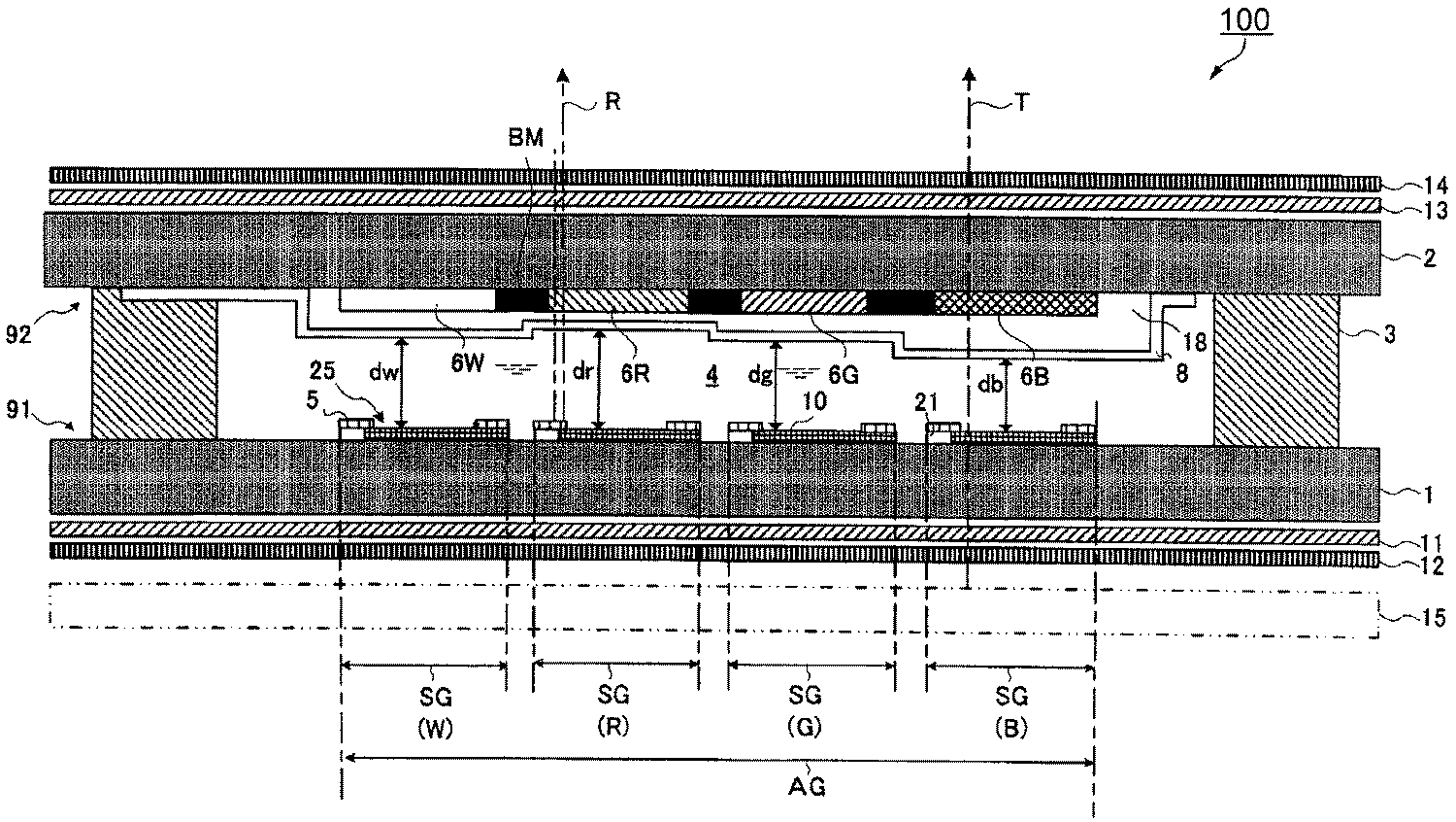
우선, 본 발명의 실시예 1에 따른 액정 표시 장치의 구성에 대하여 도 1을 이용하여 설명한다.First, the configuration of the liquid crystal display device according to the first embodiment of the present invention will be described with reference to FIG. 1.
도 1은 본 실시예에 따른 액정 표시 장치(100)의 단면 구성을 나타내는 단면도이다. 보다 상세하게는, 도 1은 액정 표시 장치(100)의 구성의 개략을 설명하기 위해, 표시 화소 AG에 포함되는 R, G, B, W(비착색)의 각 서브 화소 SG를 하나씩 추출하여 정렬한 모식 단면도이다.1 is a cross-sectional view showing a cross-sectional structure of the liquid
도 1에서, 액정 표시 장치(100)는 소자 기판(91)과, 그 소자 기판(91)에 대향하여 배치되는 컬러 필터 기판(92)이 프레임 형상의 밀봉 부재(3)를 통해 접합되고, 내부에 액정이 주입 밀봉되어 액정층(4)이 형성되어 이루어진다.In FIG. 1, in the liquid
우선, 소자 기판(91)에 대하여 설명한다. 소자 기판(91)은 유리 등의 투명한 하부 기판(1)을 갖고, 하부 기판(1)의 내면 상에는, 복수의 데이터선(32) 및 복수의 주사선(33)(도 2 참조)이 매트릭스 형상으로 배치된다. 데이터선(32) 및 주사선(33)의 교점에는, 서브 화소 SG가 마련된다. 서브 화소 SG마다에는, 화소 전극(10)이 형성되어 있다. 각 화소 전극(10)에는, 예컨대, 아몰퍼스 실리콘 TFT(Thin Film Transistor) 등의 TFT 소자(21)가 접속되어 있고, 데이터선(32) 및 주사선(33)은 각 화소 전극(10)에 대응하는 TFT 소자(21)에 전기적으로 접속되어 있다.First, the
또한, 서브 화소 SG마다, 소정 두께를 갖는 반사 전극(5)이 형성되어 있다. 반사 전극(5)은 화소 전극(10)과 도통되어 있고, 화소 전극(10)과 동시 구동된다. 각 반사 전극(5)에는, 직사각형 형상의 개구부(25)가 복수 형성되어 있다. 각 반 사 전극(5)은 알루미늄, 알루미늄 합금, 은 합금 등의 박막에 의해 형성할 수 있다. 개구부(25)는 화소 표시 영역(20)(도 2 참조) 내에 종횡의 매트릭스 형상으로 배열된 서브 화소 SG마다, 당해 서브 화소 SG의 전 면적을 기준으로 하여 소정 비율의 면적을 갖도록 형성되어 있다. 서브 화소 SG에서는, 개구부(25)에 대응하는 부분을 투과부로 하고, 그 이외의 부분을 반사부로 한다.In addition, a
다음에, 컬러 필터 기판(92)에 대하여 설명한다. 컬러 필터 기판(92)은 유리 등의 투명한 상부 기판(2)을 갖고, 상부 기판(2)의 내면 상에는, 서브 화소 SG 마다 R, G, B, W(비착색 또는 백색)의 네 개 중 어느 하나로 이루어지는 착색층(6R, 6G, 6B, 6W)이 형성되어 있다. 비착색(또는 백색)층(6W)은 투명 수지 등의 층, 혹은 투명 수지 중에 광산란성(백색성)을 부여하기 위해 투명 수지와 굴절율이 다른 미립자를 분산시킨 것으로 구성되어 있다. 착색층(6R, 6G, 6B, 6W)에 의해 컬러 필터가 구성된다(이하, 색을 구별하지 않는 경우는, 간단히 「착색층(6)」이라 칭함). 도 1에서, 하나의 표시 화소 AG는 R, G, B, W의 서브 화소 SG로 구성되는 컬러 1화소 분량의 영역을 나타내고 있다.Next, the
한쪽 서브 화소 SG로부터 다른 쪽 서브 화소 SG로의 광의 혼입을 방지하기 위해, 착색층(6) 사이에는, 흑색 차광층 BM이 형성되어 있다. 이 흑색 차광층 BM은 흑색의 수지 재료, 예컨대, 흑색의 안료를 수지 중에 분산시킨 것 등을 이용하는 것이 가능하다. 상부 기판(2) 및 착색층(6)의 내면 상에는, 투명 수지 등으로 이루어지는 오버코팅층(18)이 형성되어 있다. 이 오버코팅층(18)은 컬러 필터 기판(92)의 제조 공정 중에 사용되는 약제 등에 의한 부식이나 오염으로부터, 착색 층(6)을 보호하는 기능을 갖는다. 오버코팅층(18)의 내면 상에는, ITO(Indium-Tin- Oxide) 등이 투명한 공통 전극(8)이 형성되어 있다.In order to prevent mixing of light from one sub-pixel SG to the other sub-pixel SG, the black light shielding layer BM is formed between the colored layers 6. This black light shielding layer BM can use the black resin material, for example, the thing which disperse | distributed the black pigment in resin. On the inner surfaces of the
또한, 도 1에 나타내는 바와 같이, 각 색의 서브 화소 SG에서의 오버코팅층(18)의 두께를 조절함으로써, 각 색의 서브 화소 SG에서의 액정층(4)의 두께, 즉 셀 두께가 조절된다. 도 1에서는, R, G, B, W의 서브 화소 SG는 각각 셀 두께 dr, dg, db, dw를 갖는다. 데이터선(32) 및 주사선(33)이 동시에 화소 전극(10)에 전압을 인가했을 때에, TFT 소자(21)에 의해, 화소 전극(10) 및 반사 전극(5)과, 공통 전극(8) 사이에 전압이 인가되어, 액정층(4)의 액정이 배향 제어된다.In addition, as shown in FIG. 1, by adjusting the thickness of the
하부 기판(1)의 외면 상에는, 위상차판(1/4 파장판)(11) 및 편광판(12)이 배치되어 있고, 상부 기판(2)의 외면 상에는, 위상차판(1/4 파장판)(13) 및 편광판(14)이 배치되어 있다. 또한, 편광판(12)의 아래쪽에는, 조명 장치(15)가 배치되어 있다. 조명 장치(15)는, 예컨대, LED(Light Emitting Diode) 등과 같은 점형상 광원이나, 냉음극 형광관 등과 같은 선형상 광원과 도광판을 조합시킨 것 등이 바람직하다.On the outer surface of the
본 실시예의 액정 표시 장치(100)에서 투과형 표시가 행해지는 경우, 조명 장치(15)로부터 출사한 조명광은, 도 1에 나타내는 경로 T를 따라 진행하고, 화소 전극(10) 및 착색층(6) 등을 통과하여 관찰자에게 도달된다. 액정 표시 장치(100)는 화소 전극(10)과 공통 전극(8) 사이에 전압을 인가함으로써, 액정층(4)의 액정을 배향 제어하고, 광의 투과율을 변화시켜 계조 표시를 행한다. 또한, 조명광은 착색층(6)을 투과함으로써 소정 색상 및 밝기를 나타낸다. 이와 같이 하여, 소망 컬러 표시 화상이 관찰자에 의해 시인된다.When transmissive display is performed in the liquid
한편, 본 실시예의 액정 표시 장치(100)에 있어서 반사형 표시가 행해지는 경우, 액정 표시 장치(100)에 입사된 외광은, 도 1에 나타내는 경로 R을 따라 진행한다. 즉, 액정 표시 장치(100)에 입사된 외광은 착색층(6) 및 액정층(4)을 통과하고, 반사 전극(5)에 의해 반사되어, 재차 액정층(4) 및 착색층(6)을 통과한 후, 관찰자에게 도달된다. 액정 표시 장치(100)는, 반사 전극(5)과 공통 전극(8) 사이에 전압을 인가함으로써, 액정층(4)의 액정을 배향 제어하여, 광의 투과율을 변화시켜 계조 표시를 행한다. 또한, 외광은 착색층(6)이 형성되지 않은 영역을 통과하고, 반사 전극(5)에 의해 반사되어, 재차 착색층(6)을 통과함으로써 소정 색상 및 밝기를 나타낸다. 이와 같이 하여, 소망의 컬러 표시 화상이 관찰자에 의해 시인된다.On the other hand, when reflective display is performed in the liquid
(액정 표시 장치의 상세한 구성)(Detailed Configuration of Liquid Crystal Display Device)
여기서, 액정 표시 장치(100)의 구성에 대하여, 도 2 내지 도 5를 이용하여 더욱 상술한다.Here, the configuration of the liquid
도 2는 액정 표시 장치(100)의 구성을 모식적으로 나타내는 평면도이다. 도 2에서는, 지면 전방(관찰 쪽)에 컬러 필터 기판(92)이, 또한, 지면 안쪽에 소자 기판(91)이 각각 배치되어 있고, R, G, B, W로서 표시되는 각 영역은 하나의 서브 화소 SG를 나타내고 있다. 또, 도 2에서의 지면 세로 방향(열 방향)을 Y방향, 또한, 지면 가로 방향(행 방향)을 X방향으로 규정한다.2 is a plan view schematically illustrating the configuration of the liquid
여기에, 액정 표시 장치(100)는 R(적색), G(녹색), B(청색), W(비착색 또는 백)의 네 개를 이용하여 구성되는 컬러 표시용 액정 표시 장치이고, 또한, 스위칭 소자로서 TFT 소자(21)를 이용한 액티브 매트릭스 구동 방식의 액정 표시 장치이다. 또한, 액정 표시 장치(100)는 R, G, B, W의 각 서브 화소 SG 내에 투과 영역 및 반사 영역을 갖는 반투과 반사형 액정 표시 장치이고, 아울러, 당해 투과 영역과 당해 반사 영역에서 액정층(4)의 두께가 다른 멀티갭 구조를 갖는 액정 표시 장치이기도 하다.Here, the liquid
서브 화소 SG의 배열 구조를 도 3(a)에 나타낸다. 서브 화소 SG는 매트릭스 형상으로 배치되어 있다. 그리고, 8개의 서브 화소 SG가 대략 정방형의 표시 화소 AG를 구성한다. 이 표시 화소 AG 자체도, 또한 매트릭스 형상으로 반복하여 배치되어 있다. 바꾸어 말하면, 서브 화소 SG는 표시 화소 AG를 반복의 최소 단위로 하여 규칙적으로 배열되어 있다.The arrangement structure of the sub pixel SG is shown in Fig. 3A. Sub-pixels SG are arrange | positioned in matrix form. The eight sub-pixels SG constitute a substantially square display pixel AG. This display pixel AG itself is also arrange | positioned repeatedly in matrix form. In other words, the sub-pixels SG are regularly arranged with the display pixel AG as the minimum unit of repetition.
각 표시 화소 AG는 2행×4열의 서브 화소 SG로 구성되어 있다. 서브 화소 SG는, 어떤 표시 화소 AG에서도, 제 1 행은 RGBW, 제 2 행은 BWRG의 순서로 각각 배열되어 있다. 또한, 각 표시 화소 AG에는 RGBW의 서브 화소 SG가 각각 2개씩 포함되어 있기 때문에, 각 표시 화소 AG에서는, RGBW의 각 서브 화소 SG의 면적은 서로 같게 되어 있다. 바꾸어 말하면, 각 표시 화소 AG 내에서의 RGBW의 각 서브 화소 SG의 면적비는 1:1:1:1이다.Each display pixel AG is composed of subpixel SG of 2 rows x 4 columns. In any display pixel AG, the sub-pixels SG are arranged in the order of RGBW in the first row and BWRG in the second row, respectively. Since each display pixel AG includes two subpixels SG of RGBW, each area of each subpixel SG of RGBW is equal to each other in each display pixel AG. In other words, the area ratio of each sub-pixel SG of RGBW in each display pixel AG is 1: 1: 1: 1.
여기서, 액정 표시 장치(100)에 있어서의 표시 화소 AG는, 서브 화소 SG의 배열에 대한 반복의 최소 단위와 같은 의미를 갖는 것으로서, 표시의 최소 단위를 의미하는 것은 아니다.Here, the display pixel AG in the liquid
액정 표시 장치(100)의 화소 영역 AG는 R, G, B, W로 구성되어 있고, 종래 잘 이용되는 R, G, B로 하나의 표시 화소를 구성하는 것과는 다르다. 이에 따라, 액정 표시 장치(100)는 종래와는 다른 렌더링(rendering)을 이용하여 표시를 행하고 있다. 렌더링은 임의의 1 표시 화소 AG에서 RGB 각 색의 색상을 각각 구비한 서브 화소 SG에 인가되는 계조 신호를, 당해 표시 화소 AG 내의 서브 화소뿐만 아니라, 그 표시 화소 AG 주변에 배치된 동일 색상의 서브 화소 SG에도 중첩시켜 인가한다고 하는 화상 처리 기술을 이용하는 것이다. 즉, 하나의 표시 화소 AG에서의 RGB 각 색의 서브 화소 SG는 하나의 표시 화소 AG 주변의 표시 화소 AG에서의 동일 색상의 서브 화소 SG에도, 하나의 표시 화소 AG 내의 서브 화소 SG의 표시에 기여하는 계조 신호를 중첩하여 인가함으로써 표시를 행하는 것이다. 이에 따라, 실제의 화소수보다 높은 해상도를 시인할 수 있고, 예컨대, QVGA(Quarter Video Graphics Array) 규격에 대응하는 화면 표시 해상도를 갖는 액정 표시 장치를 이용한 경우에, VGA(Video Graphics Array) 규격에 대응하는 화면 표시 해상도를 실현한다.The pixel region AG of the liquid
도 2로 되돌아가, 소자 기판(91)은 컬러 필터 기판(92)의 1변 쪽으로부터 바깥쪽으로 돌출하여 이루어지는 돌출 영역(31)을 갖고 있고, 그 돌출 영역(31) 상에는, 드라이버 IC(40), 외부 접속용 배선(35) 및 FPC(Flexible Printed Circuit)(41) 등이 형성 또는 실장되어 있다. 드라이버 IC(40)의 입력측 단자(도시하지 않음)는 복수의 외부 접속용 배선(35)의 일단 쪽과 전기적으로 접속되어 있 고, 또한 복수의 외부 접속용 배선(35)의 타단 쪽은 FPC(41)와 전기적으로 접속되어 있다. 각 데이터선(32)은 Y방향으로 연장하도록, 또한 X방향으로 적절한 간격을 두고 형성되어 있고, 각 데이터선(32)의 일단 쪽은 드라이버 IC(40)의 출력 쪽의 단자(도시하지 않음)에 전기적으로 접속되어 있다.Returning to FIG. 2, the
각 주사선(33)은 Y방향으로 연장하도록 형성된 제 1 배선(33a)과, 그 제 1 배선(33a)의 종단부로부터 X방향으로 연장하도록 형성된 제 2 배선(33b)을 구비하고 있다. 각 주사선(33)의 제 2 배선(33b)은 각 데이터선(32)과 교차하는 방향, 즉 X방향으로 연장하도록 또한 Y방향으로 적절한 간격을 두고 형성되어 있고, 각 주사선(33)의 제 1 배선(33a)의 일단 쪽은 드라이버 IC(40)의 출력 쪽의 단자(도시하지 않음)에 전기적으로 접속되어 있다. 각 데이터선(32)과 각 주사선(33)의 제 2 배선(33b)의 교차에 대응하는 위치에는 TFT 소자(21)가 마련되어 있고, TFT 소자(21)는 데이터선(32), 주사선(33) 및 화소 전극(10) 등에 전기적으로 접속되어 있다. TFT 소자(21) 및 화소 전극(10)은 각 서브 화소 SG에 대응하는 위치에 마련된다. 화소 전극(10)은, 예컨대, ITO(Indium-Tin Oxide) 등의 투명 도전 재료에 의해 형성되어 있다.Each
화소 영역 AG가 X방향 및 Y방향으로 복수 개, 매트릭스 형상으로 배열된 영역이 화소 표시 영역(20)(2점 쇄선으로 둘러싸이는 영역)이다. 이 화소 표시 영역(20)에 문자, 숫자, 도형 등의 화상이 표시된다. 또, 화소 표시 영역(20)의 바깥쪽 영역은 표시에 기여하지 않는 프레임 영역(38)으로 되어있다. 또한, 각 데이터선(32), 각 주사선(33), 각 TFT 소자(21) 및 각 화소 전극(10) 등의 내면 상에 는, 도시하지 않은 배향막이 형성되어 있다.A region in which a plurality of pixel regions AG are arranged in the X-direction and the Y-direction and in a matrix form is the pixel display region 20 (the region enclosed by two-dot chain lines). Images such as letters, numbers, graphics, and the like are displayed in the
한편, 컬러 필터 기판(92)의 내면 상에는, 공통 전극(8)이 형성되어 있다(도 1 및 도 5 참조). 공통 전극(8)은 화소 전극(10)과 마찬가지로 ITO 등의 투명 도전 재료로 이루어지고, 컬러 필터 기판(92)의 대략 일면에 걸쳐 형성되어 있다. 공통 전극(8)은 밀봉 부재(3)의 코너 영역 E1에서 배선(15)의 일단 쪽과 전기적으로 접속되어 있고, 또한 당해 배선(15)의 타단 쪽은 드라이버 IC(40)의 COM에 대응하는 출력 단자와 전기적으로 접속되어 있다.On the other hand, the
이상의 구성을 갖는 액정 표시 장치(100)에서는, 전자기기 등과 접속된 FPC(41) 쪽으로부터의 신호 및 전력 등에 근거하여, 드라이버 IC(40)에 의해, G1, G2, …, Gm-1, Gm(m은 자연수)의 순서로 주사선(33)이 순차 배타적으로 1개씩 선택되고, 또한 선택된 주사선(33)에는, 선택 전압의 게이트 신호가 공급되는 한편, 다른 비선택의 주사선(33)에는, 비선택 전압의 게이트 신호가 공급된다. 그리고, 드라이버 IC(40)는 선택된 주사선(33)에 대응하는 위치에 있는 화소 전극(10)에 대하여, 표시 내용에 따른 소스 신호를, 각각 대응하는 S1, S2, …, Sn-1, Sn(n은 자연수)의 데이터선(32) 및 TFT 소자(21)를 통해 공급한다. 그 결과, 액정층(4)의 배향 상태가 제어되게 된다. In the liquid
다음에, 도 3(b) 등을 참조하여, 하나의 화소 영역 AG의 구성에 대하여 설명한다. 도 3(b)는, 도 2 또는 도 3(a)에 있어서의 하나의 화소 영역 AG(파선에 의해 둘러싸인 부분)에 대응하는 부분 확대 평면도이다. 도 3(b)에 나타내는 바와 같이, 하나의 화소 영역 AG는 R, G, B, W에 대응하는, 2행×4열의 서브 화소 SG를 구비하여 구성된다. 또한, R, G, B, W에 대응하는 각 서브 화소 SG는 투과형 표시가 행해지는 투과 영역 E10과, 반사형 표시가 행해지는 반사 영역 E11을 구비하여 구성된다.Next, the configuration of one pixel region AG will be described with reference to FIG. 3B and the like. FIG. 3B is a partially enlarged plan view corresponding to one pixel region AG (part enclosed by a broken line) in FIG. 2 or FIG. 3A. As shown in Fig. 3B, one pixel area AG is configured with two rows x four columns of subpixels SG corresponding to R, G, B, and W. As shown in Figs. Moreover, each sub-pixel SG corresponding to R, G, B, and W is comprised with the transmission area | region E10 in which transmissive display is performed, and the reflection area E11 in which reflective display is performed.
다음에, 도 4를 참조하여, 도 3(b)에서의 R, G, B, W에 대응하는 각 서브 화소 SG의 구성을, 반사 영역 E11의 구성과 투과 영역 E10의 구성으로 나누어 설명한다. 도 4(a)는 R, G, B, W의 각 서브 화소 SG에 대응하는 소자 기판(91)의 구성을 나타내는 부분 확대 평면도이다. 한편, 도 4(b)는 도 4(a)의 소자 기판(91)과 대향 배치되는, R, G, B, W의 각 서브 화소 SG에 대응하는 컬러 필터 기판(92)의 구성을 나타내는 부분 확대 평면도이다. 도 5(a)는 도 4(a) 및 (b)에서의 A-A'선 부분 단면도이며, R, G, B, W의 각 반사 영역 E11에 대응하는 액정 표시 장치(100)의 단면 구성을 나타낸다. 한편, 도 5(b)는 도 4(a) 및 (b)에서의 B-B'선 부분 단면도이며, R, G, B, W의 각 서브 화소 SG에 대응하는 액정 표시 장치(100)의 단면 구성을 나타낸다.Next, with reference to FIG. 4, the structure of each sub-pixel SG corresponding to R, G, B, W in FIG. 3B is divided into the structure of the reflection area E11, and the structure of the transmission area E10. FIG. 4A is a partially enlarged plan view showing the configuration of an
우선, R, G, B, W의 하나의 서브 화소 SG 내에서의 반사 영역 E11의 구성에 대하여 설명한다. 도 4(a)에 나타내는 바와 같이, 주사선(33)(도 2 참조)의 제 2 배선(33b)은 X방향으로 연장하는 본선 부분(33ba)과, 그 본선 부분(33ba)으로부터 Y방향으로 구부러지도록 분기하는 지선 부분(33bb)을 갖는다. 이들을 포함하는 주사선(33)은 하부 기판(1) 상에 배치되어 있고, 도 5(a)에는, 그 지선 부분(33bb)이 나타내어져 있다. 하부 기판(1) 및 주사선(33) 상에는, 절연성을 갖는 게이트 절연층(50)이 형성되어 있다. 게이트 절연층(50) 상으로서, 또한, 주사선(33)의 지 선 부분(33bb)과 평면적으로 겹치는 위치에는, TFT 소자(21)의 요소인 a-Si층(52)이 마련된다. 데이터선(32)은 게이트 절연층(50) 상에서, 주사선(33)과 교차하는 방향으로 연장하도록 형성되어 있다.First, the configuration of the reflection area E11 in one sub-pixel SG of R, G, B, and W will be described. As shown in Fig. 4A, the
데이터선(32)은, 도 4(a)에 나타내는 바와 같이, Y방향으로 연장하는 본선 부분(32a)과, 그 본선 부분(32a)으로부터 X방향으로 구부러지도록 분기하는 지선 부분(32b)을 갖는다. 데이터선(32)의 지선 부분(32b)의 일부분은 a-Si층(52)의 일단 쪽의 일부분 상에 형성되어 있다. a-Si층(52)의 타단 쪽의 일부분 상 및 게이트 절연층(50) 상에는, 금속 등으로 이루어지는 유지 용량 전극(16)이 형성되어 있다. 이 때문에, a-Si층(52)은 데이터선(32) 및 유지 용량 전극(16)에 각각 전기적으로 접속되어 있다. 그리고, a-Si층(52)에 대응하는 위치에는, 그 층을 요소로서 포함하는 TFT 소자(21)가 형성되어 있다.As shown in Fig. 4A, the
데이터선(32), 유지 용량 전극(16) 및 게이트 절연층(50) 등의 위에는, 절연성을 갖는 패시베이션층(반응 방지층)(51)이 형성되어 있다. 패시베이션층(51)은 유지 용량 전극(16)과 평면적으로 겹치는 위치에 콘택트 홀(개구)(51a)을 갖는다. 패시베이션층(51) 상에는, 수지 재료 등으로 이루어지는 수지층(17)이 형성되어 있다. 수지층(17)의 표면상에는, 광을 산란시키는 기능을 갖는 미세한 요철이 복수 형성되어 있다. 수지층(17)은 패시베이션층(51)의 콘택트 홀(51a)에 대응하는 위치에 콘택트 홀(17a)을 갖는다. 수지층(17) 상에는, Al(알루미늄) 등에 의해 형성되어 반사 기능을 갖는 반사 전극(5)이 형성되어 있다. 반사 전극(5)은 미세한 요철을 복수 가진 수지층(17) 상에 형성되어 있기 때문에, 그 미세한 복수의 요철을 반영한 형상으로 형성되어 있다. 콘택트 홀(51a, 17a)에 대응하는 반사 전극(5)의 위치에는, 광을 투과시키는 투과 개구 영역(25)이 형성되어 있다. 반사 전극(5) 상 및 투과 개구 영역(25)에는, 화소 전극(10)이 형성되어 있다.An insulating passivation layer (reaction prevention layer) 51 is formed on the
한편, R, G, B의 하나의 서브 화소 SG 내에서의 반사 영역 E11에 대응하는 컬러 필터 기판(92)의 구성은 다음과 같다.On the other hand, the configuration of the
하부 기판(1)과 동일한 재료에 의해 이루어지는 상부 기판(2) 상으로서, 또한, 반사 영역 E11에 대응하는 위치에는, R, G, B의 착색층(6)이 형성되어 있다. 각 착색층(6)의 두께는 d3으로 설정되어 있다. 착색층(6)은 투과 영역 E10과 반사 영역 E11로 균일한 색을 표시시키는 기능을 갖는 개구(6a)를 갖는다. 서로 인접하는 착색층(6)을 구획하는 위치에는, 흑색 차광층 BM이 형성되어 있다. 착색층(6) 상에는, 수지 재료 등으로 이루어지는 오버코팅층(18)이 형성되어 있다. 오버코팅층(18)의 두께는 d4로 설정된다. 오버코팅층(18)의 두께 d4를 서브 화소 SG 마다 조정함으로써, R, G, B, W의 각 반사 영역 E11에 대응하는 액정층(4)의 두께(셀 두께) d2를, 서브 화소 SG마다 변경할 수 있다. 오버코팅층(18) 등의 위에는, 공통 전극(8)이 형성되어 있다.The
이상에서 기술한 반사 영역 E11에 대응하는 소자 기판(91)과, 당해 반사 영역 E11에 대응하는 컬러 필터 기판(92)은 액정층(4)을 개재하여 대향하고 있다. 그리고, 반사 영역 E11에 대응하는 액정층(4)의 두께는, 상기한 바와 같이, d2로 설정되어 있다.The
다음에, R, G, B, W의 하나의 서브 화소 영역 SG 내에서의 투과 영역 E10의 구성에 대하여 설명한다.Next, the configuration of the transmission region E10 in one sub pixel region SG of R, G, B, and W will be described.
하부 기판(1) 상에는, 도 5(b)에 나타내는 바와 같이, 게이트 절연층(50)이 형성되어 있다. 게이트 절연층(50) 상에는, 패시베이션층(51)이 형성되어 있다. 패시베이션층(51) 상에는, 수지층(17)이 형성되어 있다. 상기한 바와 같이, 반사 영역 E11에 형성된 수지층(17)은 그 표면상에 미세한 요철이 형성되어 있는데 대하여, 투과 영역 E10에 형성된 수지층(17)은 그 표면상에 미세한 요철은 형성되어 있지 않다. 즉, 투과 영역 E10에 형성된 수지층(17)의 표면은 대략 평탄성을 갖도록 형성되어 있다. 수지층(17) 상에는, 화소 전극(10)이 형성되어 있다.On the
한편, R, G, B, W의 하나의 서브 화소 영역 SG 내에서의 투과 영역 E10에 대응하는 컬러 필터 기판(92)의 구성은 다음과 같다. 상부 기판(2) 상에는, 착색층(6)이 형성되어 있다. 그 각 착색층(6) 상에는, 두께 d5의 오버코팅층(18)이 형성되어 있다. 오버코팅층(18)은, 두께 d5를 조정함으로써, R, G, B, W의 각 투과 영역 E10에 대응하는 액정층(4)의 두께(셀 두께) d1을 서브 화소 SG마다 변경할 수 있다. 오버코팅층(18) 상에는 공통 전극(8)이 형성되어 있다. 또한, 상부 기판(2)의 외면 상에는 위상차판(11)이 배치되어 있고, 또한 위상차판(11)의 외면 상에는 편광판(12)이 배치되어 있다.On the other hand, the configuration of the
이상에서 설명한 투과 영역 E10에 대응하는 소자 기판(91)과, 당해 투과 영역 E10에 대응하는 컬러 필터 기판(92)은 액정층(4)을 개재하여 대향하고 있다. 또한, 각 서브 화소 SG에서, 투과 영역 E10의 오버코팅층(18)의 두께 d5와, 반사 영역 E11의 오버코팅층(18)의 두께 d4가 다르도록 설정되어 있다. 이에 따라, 투 과 영역 E10의 액정층(4)의 두께 d1은 반사 영역 E11의 액정층(4)의 두께 d2보다 크게 되어 있고, 이른바 멀티갭 구조를 이루고 있다.The
이것에 더하여, 투과 영역 E10의 액정층(4)의 두께 d1은, 도 1의 설명에서 설명한 바와 같이, R, G, B, W의 서브 화소 SG에서 각각 dr, dg, db, dw의 값을 취한다. 또한, 반사 영역 E11의 액정층(4)의 두께 d2도, 두께 d1과 마찬가지로 하여 서브 화소 SG마다 값이 설정된다. 따라서, 액정층(4)의 셀 두께는 최대로 8개의 다른 값을 취하는 것으로 된다. 두께 d2를 서브 화소마다 다르게 한 취지는 두께 d1에 대한 취지와 마찬가지이므로, 본 예에서는 두께 d1(dr, dg, db, dw)에 관련되는 사항에 대해서만 설명한다.In addition, the thickness d1 of the
(셀 두께의 크기와 투과율의 관계)(Relationship between Cell Thickness and Transmittance)
다음에 셀 두께의 크기와 투과율의 관계에 대하여 기술한다. 도 6은, 일반적인 액정 표시 장치에 있어서의, 각 색의 서브 화소에서의 인가 전압과 투과율의 관계를 나타내는 그래프이다. 이 일반적인 액정 표시 장치는 RGB 각 색의 서브 화소로 구성되고, 노멀리 화이트의 액정 표시 장치이다. 또한, 이 일반적인 액정 표시 장치에 있어, RGB 각 색의 서브 화소에 있어서의 셀 두께는 모두 같은 일정한 두께로 되어 있다. 여기서, 가로축은 서브 화소에서의 화소 전극(10)과 공통 전극(8) 사이에 인가되는 인가 전압의 크기를 나타내고, 세로축은 RGB 각 색의 서브 화소에서의 광의 투과율을 나타내고 있다. 여기서, RGB의 서브 화소의 광의 투과율은 액정층(4)의 액정의 배향 상태에 따라 결정된다.Next, the relationship between the size of the cell thickness and the transmittance will be described. 6 is a graph showing a relationship between an applied voltage and a transmittance in subpixels of respective colors in a general liquid crystal display device. This general liquid crystal display device is composed of sub-pixels of respective RGB colors, and is a normally white liquid crystal display device. Moreover, in this general liquid crystal display device, the cell thickness in the sub pixel of each RGB color is all the same constant thickness. Here, the horizontal axis represents the magnitude of the applied voltage applied between the
도 6에서, 인가 전압을 올려 가면, 어떤 일정한 전압 Vc까지는, R의 서브 화소, G의 서브 화소, B의 서브 화소 각각에 있어서의 광의 투과율에 변화는 없다. 그러나, 인가 전압이 전압 Vc보다 커지는 경우, 즉 중간조 표시의 경우, 액정층(4)의 액정 배향 상태가 변화되어, R의 서브 화소, G의 서브 화소, B의 서브 화소 각각에서의 광의 투과율도 그에 따라 변화된다. 인가 전압이 전압 Vc보다 커지는 경우, 각 색의 서브 화소에서의 광의 투과율을 나타내는 곡선(이하, 단지 「VT 커브」라고 함)은 급격히 하강하는 특성을 나타낸다. 즉, 각 색의 서브 화소에서의 광의 투과율은 저하한다. 각 색의 서브 화소에서의 VT 커브의 하강 쪽의 특성은 각 색의 서브 화소마다 다르고, R의 서브 화소에서의 투과율 저하가 가장 크고, B의 서브 화소에서의 투과율 저하가 가장 작다. 따라서, 인가 전압이 전압 Vc보다 커지는 경우, 각 색의 서브 화소의 투과율은, 높은 순서대로, B의 서브 화소, G의 서브 화소, R의 서브 화소의 순으로 된다. 따라서, 일반적인 액정 표시 장치에서는, 상기한 바와 같이, 각 서브 화소의 셀 두께가 같은 경우에는, 같은 계조의 중간조 표시에서 전 화소의 표시를 행하면 항상 청색을 띤 백색 표시로 된다.In FIG. 6, when the applied voltage is raised, there is no change in the transmittance of light in each of the subpixels of R, the subpixels of G, and the subpixels of B up to a certain constant voltage Vc. However, when the applied voltage becomes larger than the voltage Vc, that is, in the case of halftone display, the liquid crystal alignment state of the
또, 가로축을, 반사 전극(5)과 공통 전극(8) 사이에 인가되는 인가 전압의 크기로 하고, 세로축을 서브 화소의 광의 반사율로 하여도, 서브 화소의 광의 반사율은 액정층(4)의 액정 배향 상태에 따라 결정되는 값이므로, 도 6과 마찬가지의 특성을 나타내는 그래프로 된다. 따라서, 이 경우에 있어서도, 인가 전압이 전압 Vc보다 커지는 경우에 있어서의 각 색의 서브 화소의 투과율은, 높은 순서대로, B의 서브 화소, G의 서브 화소, R의 서브 화소의 순으로 된다. 따라서, 이 때도, 각 서브 화소의 셀 두께가 같은 경우에는, 같은 계조의 중간조 표시에서 전 화소의 표시를 행하는 경우, 항상 청색을 띤 백색 표시로 된다.Further, even when the horizontal axis is the magnitude of the applied voltage applied between the
그래서, 이러한 컬러화를 억제하기 위해, 본 실시예에 따른 액정 표시 장치(100)에서는, 액정층(4)의 복굴절율 Δn과 셀 두께의 두께 d의 곱으로 규정되는 리타데이션값 Δn·d를, R≥G≥B로 되도록 설정한다. 구체적으로는, R광의 파장을 λr(650㎚ 정도), G광의 파장을 λg(550㎚ 정도), B광의 파장을 λb(400㎚ 정도), λr, λg, λb에서의 액정층(4)의 복굴절율을 각각 Δnr, Δng, Δnb로 하고, R, G, B 각각의 서브 화소 SG의 셀 두께를 dr, dg, db라고 하면, R, G, B 각각의 서브 화소 SG에서의 리타데이션값과 광의 파장의 비 Δnr·dr/λr, Δng·dg/λg, Δnb·db/λb는 각각 같은 크기의 값으로 설정된다. 여기서, 액정층(4)의 복굴절율 Δn은 통과하는 광의 파장에 따라 다르지만, 거의 일정하다.Therefore, in order to suppress such colorization, in the liquid
따라서, 각 색의 서브 화소 SG에서의 셀 두께는 dr≥dg≥db(단, dr=dg=db로 되지는 않음)의 관계가 성립한다. 또, 각 색의 서브 화소 SG의 리타데이션값의 범위로는, 360㎚≤R(=Δnr·dr)≤700㎚, 340㎚≤G(=Δng·dg)≤600㎚, 340㎚≤B(=Δnb·db)≤500㎚로 된다.Therefore, the cell thickness in the sub-pixel SG of each color has a relationship of dr≥dg≥db (but not dr = dg = db). Moreover, as a range of the retardation value of sub-pixel SG of each color, 360 nm <= R (= (DELTA) nr * dr) <= 700nm, 340nm <= G (= (DELTA) ng.dg) <= 600nm, 340nm <= B ( = Δnb · db) ≤ 500 nm.
이와 같이 RGB의 각 색의 서브 화소 SG의 셀 두께를 설정하는 것으로, 각 색의 서브 화소 SG를 출광하는 광은, 액정층(4)을 통과할 때, 간섭에 의해 강하게 합쳐진다. 이에 따라, 본 실시예에 따른 액정 표시 장치(100)에서는, 도 6에 나타낸 각 색의 서브 화소 SG의 VT 커브를 일치시킬 수 있고, 서브 화소 SG에 인가되는 인가 전압의 크기가 전압 Vc 이상으로 되는 값이더라도, 백색 표시 시의 컬러화를 억 제할 수 있다.By setting the cell thickness of the sub-pixel SG of each color of RGB in this way, the light which outgoes the sub-pixel SG of each color is strongly merged by interference, when passing through the
본 실시예에 따른 액정 표시 장치(100)에서는, 또한 W의 서브 화소 SG를 갖는다. W의 서브 화소 SG에서의 리타데이션값 Δnw·dw는 R광의 파장 λr과 B광의 파장 λb 사이에 설정된다. 즉, W의 서브 화소 SG에서의 셀 두께 dw는 dr≥dw≥db(단, dr=dw=db로 되지는 않음)의 관계가 성립하는 값으로 설정된다. W의 서브 화소 SG에서의 리타데이션값 Δnw·dw를, R광의 파장 λr에 가까운 값으로 설정하면, 백색 표시 시에, W의 서브 화소 SG에서의 R광의 투과 효율이 높아져, 적색을 띠는 백색 표시로 된다. 마찬가지로, B광의 파장 λb에 가까운 값으로 설정하면, 백색 표시 시에, W의 서브 화소 SG에서의 B광의 투과 효율이 높아져, 청색을 띠는 백색 표시로 된다. 이와 같이, W의 서브 화소 SG에서의 리타데이션값 Δnw·dw를 조정하는 것으로, 즉, 셀 두께 dw를 조정하는 것에 의해, 화이트 밸런스를 소정 색 온도(color temperature)의 상태로 설정할 수 있어, 사용자에 있어 소망의 백색 표시를 실현할 수 있다.In the liquid
(화이트 밸런스의 조정의 응용예)(Application example of adjustment of the white balance)
본 실시예의 액정 표시 장치(100)는, 도 3(a)에 나타내는 바와 같이, 표시 화소 AG에서의 R, G, B, W의 서브 화소 SG의 면적이 전부 같다. 이러한 경우에는, R, G, B의 3색의 서브 화소 SG의 면적비에 기인한 화이트 밸런스의 편차는 발생하지 않는다. 이 때문에, W의 서브 화소 SG에서의 리타데이션값 Δnw·dw의 조정에 있어서는, λr에 접근시켜 적색을 띠는 백 표시로 하거나, λb에 접근시켜 청색을 띠는 백 표시로 하거나 할 필요는 없다. 따라서, W의 서브 화소 SG의 셀 두께 dw는 시감도가 가장 높게 휘도를 확보하기 쉬운 G의 파장에 가까운 값, 즉, dr≥dw≒dg≥db(단, dr=dw=db로 되지는 않음)로 되는 값으로 설정한다. 또는, W의 서브 화소 SG에서의 리타데이션값 Δnw·dw는 G의 서브 화소 SG에서의 리타데이션값 Δng·dg과 같게 되도록 설정한다. 이러한 구성에 의하면, 휘도가 높은 표시를 할 수 있다.In the liquid
하기 표 1은, 액정 표시 장치(100)에 있어서, G의 서브 화소 SG의 셀 두께 dg를 3.0㎛에서 일정하게 한 경우에, W의 서브 화소 SG의 셀 두께 dw를 2.6㎛ 또는 3.0㎛으로 했을 때의 휘도를 비교한 것이다. 이 표로부터, 셀 두께 dw를 셀 두께 dg와 같게 하는(즉 3.0㎛로 함) 것에 의해, 표시의 휘도가 높아지는 것을 알 수 있다.Table 1 below shows that in the liquid

<실시예 2><Example 2>
계속해서, 본 발명의 실시예 2에 따른 액정 표시 장치(200)에 대하여 설명한다. 액정 표시 장치(200)는 각 표시 화소 AG에서의 서브 화소 SG의 배열 구조가 실시예 1의 액정 표시 장치(100)와 다른 것이다. 그 밖의 구성에 대해서는 액정 표시 장치(100)와 마찬가지이므로, 이하의 설명에 이용하는 각 도면에서는, 액정 표시 장치(100)와 동일한 구성 요소에는 동일한 부호를 부여하고 설명은 생략한다.Subsequently, the liquid
(액정 표시 장치의 구성)(Configuration of Liquid Crystal Display)
도 7은 본 실시예에 따른 액정 표시 장치(200)의 개략 구성을 모식적으로 나타내는 평면도이다. 액정 표시 장치(200)는 각 표시 화소 AG가 2행×3열의 6개의 서브 화소 SG로 이루어지는 점에서 액정 표시 장치(100)와 다르다.7 is a plan view schematically illustrating a schematic configuration of a liquid
액정 표시 장치(200)에서의 표시 화소 AG 내의 서브 화소 SG의 배열 구조를, 도 8에 나타낸다. 표시 화소 AG는 2행3열의 서브 화소 SG를 갖고, 2개의 R의 서브 화소 SG, 2개의 G의 서브 화소 SG, 하나의 B의 서브 화소 SG, 하나의 W(비착색 또는 백색)의 서브 화소 SG의 6개의 서브 화소 SG로 구성된다. 보다 상세하게는, 제 1 행은 RBG, 제 2 행은 GWR의 순서로 각각 배열되어 있다. 액정 표시 장치(200)의 화소 표시 영역(20)(도 7 참조)에는, 이러한 표시 화소 AG가 매트릭스 형상으로 반복 배열되어 있다. 여기서, 액정 표시 장치(200)에 있어서의 표시 화소 AG는 서브 화소 SG의 배열에 대한 반복의 최소 단위와 같은 의미를 갖는 것으로서, 표시의 최소 단위를 의미하는 것은 아니다. 액정 표시 장치(200)는, 액정 표시 장치(100)와 마찬가지로, 렌더링을 이용하여 표시한다.The arrangement structure of sub-pixel SG in display pixel AG in the liquid
여기서, B의 서브 화소 SG의 수가 R나 G의 서브 화소 SG의 수에 비하여 적은 이유는, B의 서브 화소 SG는 G나 R과 비교하여 휘도 정보를 그다지 가지고 있지 않고, 색의 밸런스를 취하고 있는 것에 불과하기 때문에, W의 서브 화소 SG로 바꾸는 것에 의해 각별하게 휘도를 향상시킬 수 있기 때문이다. 이와 같이, 표시 화소 AG의 화소 배열 구조에서는, RGB의 각 서브 화소 SG를 액정 표시 장치 상에서 균등하게 배치하는 것은 아니고, RGB 각각의 서브 화소 SG의 면적 및 배치를, 인간의 색에 대한 시각 특성을 고려하여 최적화하고 있다. 그 때문에, 도 8에 나타내는 표시 화소 AG를 갖는 액정 표시 장치(200)에서는, 일반적인 액정 표시 장치에 비해 적은 서브 화소수로 인간의 시각에 있어서의 고화질의 표시를 실현할 수 있다.The reason why the number of subpixels SG of B is smaller than the number of subpixels SG of R or G is that the subpixels SG of B do not have much luminance information compared with G or R, and have a color balance. This is because the brightness can be improved significantly by changing to the sub-pixel SG of W. In this way, in the pixel array structure of the display pixels AG, the RGB sub-pixels SG are not evenly arranged on the liquid crystal display device, but the area and the arrangement of each of the RGB sub-pixels SG are not changed. We are considering and optimizing. Therefore, in the liquid
(화이트 밸런스 조정의 응용예)(Application example of white balance adjustment)
도 8에 나타내는 표시 화소 AG에서는, B의 서브 화소 SG의 수가 R이나 G의 서브 화소 SG의 수에 비하여 적으므로, 표시 화소 AG 전체에서 보면, B의 서브 화소 SG의 면적은 R이나 G의 서브 화소 SG의 면적에 비하여 작게된다. 구체적으로는, 표시 화소 AG는 RGB의 서브 화소 SG 중 B의 서브 화소 SG와 W의 서브 화소 SG의 합계 면적이 다른 2색의 서브 화소 SG 각각의 면적과 대략 같게 구성되어 있다. 도 8에 나타내는 표시 화소 AG에서는, 일례로서, 표시 화소 AG는 상기 RGB 및 비착색의 각 색의 서브 화소 SG의 면적 비율이 2:2:1:1로 되어 있다. 이러한 화소 배열 구조의 표시 화소 AG를 갖는 액정 표시 장치(200)에 있어서, 백색 표시를 행하는 경우, B색의 광이 부족하게 되므로, 황색을 띠는 백색 표시로 된다. 본 실시예에 따른 액정 표시 장치(200)에서는, 이러한 백색 표시에서의 컬러화를 억제하기 위해, W의 서브 화소 SG에서의 리타데이션값 Δnw·dw를 B의 서브 화소 SG에서의 리타데이션값 Δnb·db에 가까운 값으로 설정하는 것으로 한다. 즉, W의 서브 화소 SG에서의 셀 두께를 조정하여, B의 셀 두께와 거의 같게 설정한다. 이에 따라, W의 서브 화소 SG로부터 출광되는 광은 B색의 성분이 강조되어, 부족한 B색의 광을 보충할 수 있어, B의 서브 화소 SG의 면적이 작은 것에 따라 발생하는 백색 표시에 있어서의 상술한 컬러화를 억제할 수 있다. 이와 같이 하는 것에 의해, W의 서브 화소 SG에서의 셀 두께를 조정하여, B광의 성분을 강조함으로써, 표시 화소 AG에서의 B색의 광을 보충할 수 있어, 백색 표시의 컬러화를 억제할 수 있다.In the display pixel AG shown in FIG. 8, since the number of subpixels SG of B is smaller than the number of subpixels SG of R or G, the area of the subpixel SG of B is the subfield of R or G when viewed in the entire display pixel AG. It becomes small compared with the area of the pixel SG. Specifically, the display pixel AG is configured such that the total area of the subpixel SG of B and the subpixel SG of W among the subpixels SG of RGB is approximately equal to the area of each of the two subpixels SG of different colors. In display pixel AG shown in FIG. 8, as an example, as for display pixel AG, the area ratio of the sub-pixel SG of each color of said RGB and non-coloring is 2: 2: 1: 1. In the liquid
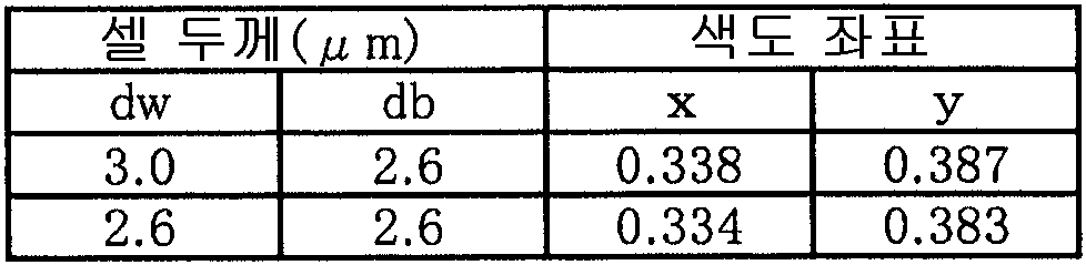
하기 표 2는, 액정 표시 장치(200)에 있어서, B의 서브 화소 SG의 셀 두께 db를 2.6㎛에서 일정으로 한 경우에, W의 서브 화소 SG의 셀 두께 dw를 3.0㎛ 또는 2.6㎛으로 했을 때의 백 표시의 색도 좌표를 나타낸 것이다. 또한, 도 9는 표 2의 색도 좌표를 x-y 좌표 상에 플로팅한 것이다. 이들 표 및 도면으로부터, 셀 두께 dw를 셀 두께 db와 같게 (2.6㎛로) 함으로써, 백 표시의 색 좌표가 백점에 접근하는 것을 알 수 있다(도 9 중 파선의 화살표).Table 2 below shows that in the liquid
상술한 응용예에서는, B의 서브 화소 SG의 면적이 다른 색의 서브 화소 SG와 비교하여 작은 경우에 대하여 기술했지만, B의 서브 화소 SG에 한하지 않고, 다른 색의 서브 화소 SG의 면적이 작은 경우에도, 본 발명의 수법을 이용할 수 있는 것은 물론이다. 이 때, 표시 화소 AG는 RGB의 서브 화소 SG 중 1색의 서브 화소 SG와 W의 서브 화소 SG의 합계 면적이, 다른 2색의 서브 화소 SG 각각의 면적과 대략 같게 구성되어 있다. 이 경우, W의 서브 화소 SG의 셀 두께를 조정하여, W의 서브 화소 SG의 셀 두께를, 표시 화소 AG에서의 서브 화소 SG의 면적이 가장 작은 색의 셀 두께와 거의 같게 되도록 설정한다. 이와 같이 하는 것에 의해, W의 서브 화소 SG로부터 출광되는 광은, 표시 화소 AG에서의 서브 화소 SG의 면적이 가장 작은 색의 광의 성분을 강조하여 출광할 수 있고, 표시 화소 AG에서의 그 색의 광이 부족한 것을 보충할 수 있다. 이와 같이, W의 서브 화소 SG의 셀 두께를, 서브 화소 SG의 면적이 가장 작은 색의 셀 두께와 거의 같게 설정함으로써, 백색 표시에서의 화이트 밸런스를 소정 색 온도(color temperature)의 상태로 설정할 수 있어, 백색 표시에서의 컬러화를 억제할 수 있다.In the above-described application example, the case where the area of the subpixel SG of B is smaller than that of the subpixel SG of another color is described. However, the area of the subpixel SG of another color is small, not limited to the subpixel SG of B. Even in this case, it goes without saying that the method of the present invention can be used. At this time, the display pixel AG is configured such that the total area of the subpixel SG of one color and the subpixel SG of W of the RGB subpixels SG is approximately equal to the area of each of the two subpixels SG of different colors. In this case, the cell thickness of the subpixel SG of W is adjusted to set the cell thickness of the subpixel SG of W so that the area of the subpixel SG in the display pixel AG is approximately equal to the cell thickness of the smallest color. In this way, the light emitted from the sub-pixel SG of W can be emitted by emphasizing the component of the light of the color having the smallest area of the sub-pixel SG in the display pixel AG. Can compensate for the lack of light. Thus, by setting the cell thickness of the subpixel SG of W to be almost equal to the cell thickness of the color of the smallest subpixel SG, the white balance in the white display can be set to a state of a predetermined color temperature. Therefore, colorization in the white display can be suppressed.
(전자기기)(Electronics)
다음에, 본 실시예에 따른 액정 표시 장치(100)(액정 표시 장치(200)를 포함함. 이하 동일)를 적용할 수 있는 전자기기의 구체예에 대하여 도 10을 참조하여 설명한다.Next, a specific example of the electronic apparatus to which the liquid crystal display device 100 (including the liquid
우선, 본 실시예에 따른 액정 표시 장치(100)를, 휴대형 퍼스널 컴퓨터(이른바 노트북 컴퓨터)의 표시부에 적용한 예에 대하여 설명한다. 도 10(a)는 이 퍼스널 컴퓨터의 구성을 나타내는 사시도이다. 동 도면에 나타내는 바와 같이, 퍼스널 컴퓨터(710)는 키보드(711)를 구비한 본체부(712)와, 본 발명에 따른 액정 표시 장치(100)를 적용한 표시부(713)를 구비하고 있다.First, an example in which the liquid
계속해서, 본 실시예에 따른 액정 표시 장치(100)를, 휴대 전화기의 표시부에 적용한 예에 대하여 설명한다. 도 10(b)는 이 휴대 전화기의 구성을 나타내는 사시도이다. 동 도면에 나타내는 바와 같이, 휴대 전화기(720)는 복수의 조작 버튼(721) 외에, 수화구(722), 송화구(723)와 함께, 본 실시예에 따른 액정 표시 장치(100)를 적용한 표시부(724)를 구비한다.Subsequently, an example in which the liquid
또, 본 실시예에 따른 액정 표시 장치(100)를 적용할 수 있는 전자기기로는, 도 10(a)에 나타내는 퍼스널 컴퓨터나 도 10(b)에 나타내는 휴대 전화기 외에도, 액정 텔레비전, 뷰파인더형·모니터 직시형 비디오 테이프 레코더, 카 네비게이션 장치, 호출기, 전자 수첩, 전자 계산기, 워드 프로세서, 워크 스테이션, 화상 전화, POS 단말, 디지털 스틸 카메라 등을 들 수 있다.As the electronic device to which the liquid
본 발명에 의하면, 투명(W)의 서브 화소를 갖는 액정 표시 장치에 있어서, 화이트 밸런스를 조정할 수 있다.According to the present invention, in the liquid crystal display device having the transparent (W) sub-pixel, the white balance can be adjusted.
Claims (10)
Applications Claiming Priority (4)
| Application Number | Priority Date | Filing Date | Title |
|---|---|---|---|
| JPJP-P-2005-00197073 | 2005-07-06 | ||
| JP2005197073 | 2005-07-06 | ||
| JPJP-P-2006-00163117 | 2006-06-13 | ||
| JP2006163117A JP4501899B2 (en) | 2005-07-06 | 2006-06-13 | Liquid crystal display device and electronic device |
Publications (2)
| Publication Number | Publication Date |
|---|---|
| KR20070005506A KR20070005506A (en) | 2007-01-10 |
| KR100825148B1 true KR100825148B1 (en) | 2008-04-24 |
Family
ID=37617999
Family Applications (1)
| Application Number | Title | Priority Date | Filing Date |
|---|---|---|---|
| KR1020060062803A Active KR100825148B1 (en) | 2005-07-06 | 2006-07-05 | Liquid crystal display and electronics |
Country Status (3)
| Country | Link |
|---|---|
| US (1) | US20070008463A1 (en) |
| JP (1) | JP4501899B2 (en) |
| KR (1) | KR100825148B1 (en) |
Families Citing this family (8)
| Publication number | Priority date | Publication date | Assignee | Title |
|---|---|---|---|---|
| JP5032157B2 (en) * | 2007-03-05 | 2012-09-26 | 株式会社ジャパンディスプレイセントラル | Liquid crystal display |
| JP2010169704A (en) | 2009-01-20 | 2010-08-05 | Casio Computer Co Ltd | Liquid crystal display apparatus |
| JP4877363B2 (en) | 2009-06-29 | 2012-02-15 | カシオ計算機株式会社 | Liquid crystal display device and driving method thereof |
| WO2011093243A1 (en) * | 2010-01-29 | 2011-08-04 | シャープ株式会社 | Liquid crystal display device |
| JP6098196B2 (en) * | 2013-02-05 | 2017-03-22 | セイコーエプソン株式会社 | Electro-optical device and electronic apparatus |
| JP2015025835A (en) * | 2013-07-24 | 2015-02-05 | セイコーエプソン株式会社 | Color filter substrate, electro-optic device, projection type display device, and manufacturing method of color filter substrate |
| US10388705B2 (en) * | 2014-05-27 | 2019-08-20 | Lg Display Co., Ltd. | Display panel and method for manufacturing thereof |
| CN105404052A (en) * | 2016-01-05 | 2016-03-16 | 京东方科技集团股份有限公司 | Curved-surface display panel |
Citations (1)
| Publication number | Priority date | Publication date | Assignee | Title |
|---|---|---|---|---|
| JP2004004822A (en) | 2002-05-04 | 2004-01-08 | Samsung Electronics Co Ltd | Four-color drive liquid crystal display device and display panel used therefor (LIQUID CRYSTALD DISPLAY SUSING 4 COLORAND PANEL FOR THE SAME) |
Family Cites Families (58)
| Publication number | Priority date | Publication date | Assignee | Title |
|---|---|---|---|---|
| DE3650639T2 (en) * | 1985-01-25 | 1998-02-26 | Nippon Electric Co | Construction of a liquid crystal multicolor display panel |
| JP3029489B2 (en) * | 1991-07-25 | 2000-04-04 | キヤノン株式会社 | Display device |
| JPH07128640A (en) * | 1993-10-29 | 1995-05-19 | Sharp Corp | Ferroelectric liquid crystal display device |
| US5673127A (en) * | 1993-12-01 | 1997-09-30 | Matsushita Electric Industrial Co., Ltd. | Display panel and display device using a display panel |
| KR0156765B1 (en) * | 1993-12-27 | 1998-11-16 | 사토 후미오 | Display device |
| US7123216B1 (en) * | 1994-05-05 | 2006-10-17 | Idc, Llc | Photonic MEMS and structures |
| US7138984B1 (en) * | 2001-06-05 | 2006-11-21 | Idc, Llc | Directly laminated touch sensitive screen |
| US6573961B2 (en) * | 1994-06-27 | 2003-06-03 | Reveo, Inc. | High-brightness color liquid crystal display panel employing light recycling therein |
| US5936693A (en) * | 1994-09-27 | 1999-08-10 | Casio Computer Co., Ltd. | Liquid crystal display device having a wide view angle |
| US6560018B1 (en) * | 1994-10-27 | 2003-05-06 | Massachusetts Institute Of Technology | Illumination system for transmissive light valve displays |
| JPH08294137A (en) * | 1995-04-20 | 1996-11-05 | Mitsubishi Electric Corp | Projector device |
| US7289174B1 (en) * | 1995-07-17 | 2007-10-30 | Seiko Epson Corporation | Reflective type color liquid crystal device and an electronic apparatus using this |
| JP3575024B2 (en) * | 1995-07-17 | 2004-10-06 | セイコーエプソン株式会社 | Reflective color liquid crystal device and electronic equipment using the same |
| JPH09197445A (en) * | 1996-01-16 | 1997-07-31 | Fujitsu Ltd | Color liquid crystal panel |
| US6072555A (en) * | 1996-02-01 | 2000-06-06 | Canon Kabushiki Kaisha | Display apparatus capable of gradational display |
| US5899550A (en) * | 1996-08-26 | 1999-05-04 | Canon Kabushiki Kaisha | Display device having different arrangements of larger and smaller sub-color pixels |
| US6016178A (en) * | 1996-09-13 | 2000-01-18 | Sony Corporation | Reflective guest-host liquid-crystal display device |
| JPH10170905A (en) * | 1996-12-09 | 1998-06-26 | Alps Electric Co Ltd | Color polarization filter for reflection and reflection-type color liquid crystal display device using the filter |
| US6124909A (en) * | 1996-12-25 | 2000-09-26 | Casio Computer Co., Ltd. | Color liquid crystal display device having a plurality of pixel areas which emit non-colored light |
| US6195140B1 (en) * | 1997-07-28 | 2001-02-27 | Sharp Kabushiki Kaisha | Liquid crystal display in which at least one pixel includes both a transmissive region and a reflective region |
| US6215538B1 (en) * | 1998-01-26 | 2001-04-10 | Sharp Kabushiki Kaisha | Liquid crystal display including both color filter and non-color filter regions for increasing brightness |
| JP3368823B2 (en) * | 1998-04-15 | 2003-01-20 | カシオ計算機株式会社 | Liquid crystal display device |
| WO2000020918A1 (en) * | 1998-10-07 | 2000-04-13 | Seiko Epson Corporation | Liquid crystal device and electronic apparatus |
| WO2003007049A1 (en) * | 1999-10-05 | 2003-01-23 | Iridigm Display Corporation | Photonic mems and structures |
| US7283142B2 (en) * | 2000-07-28 | 2007-10-16 | Clairvoyante, Inc. | Color display having horizontal sub-pixel arrangements and layouts |
| US7274383B1 (en) * | 2000-07-28 | 2007-09-25 | Clairvoyante, Inc | Arrangement of color pixels for full color imaging devices with simplified addressing |
| EP1331513A4 (en) * | 2000-10-17 | 2008-04-02 | Toshiba Matsushita Display Tec | Liquid crystal display and its producing method |
| US7184066B2 (en) * | 2001-05-09 | 2007-02-27 | Clairvoyante, Inc | Methods and systems for sub-pixel rendering with adaptive filtering |
| US7221381B2 (en) * | 2001-05-09 | 2007-05-22 | Clairvoyante, Inc | Methods and systems for sub-pixel rendering with gamma adjustment |
| US6714206B1 (en) * | 2001-12-10 | 2004-03-30 | Silicon Image | Method and system for spatial-temporal dithering for displays with overlapping pixels |
| KR100870003B1 (en) * | 2001-12-24 | 2008-11-24 | 삼성전자주식회사 | Liquid crystal display |
| US20040051724A1 (en) * | 2002-09-13 | 2004-03-18 | Elliott Candice Hellen Brown | Four color arrangements of emitters for subpixel rendering |
| TWI227340B (en) * | 2002-02-25 | 2005-02-01 | Himax Tech Inc | Color filter and liquid crystal display |
| JP4200830B2 (en) * | 2002-10-11 | 2008-12-24 | セイコーエプソン株式会社 | Electro-optical device manufacturing method, electro-optical device, and electronic apparatus |
| KR100907479B1 (en) * | 2002-12-31 | 2009-07-13 | 삼성전자주식회사 | Color filter substrate and liquid crystal display having the same |
| KR20040080778A (en) * | 2003-03-13 | 2004-09-20 | 삼성전자주식회사 | Liquid crystal displays using 4 color and panel for the same |
| JP4366988B2 (en) * | 2003-05-01 | 2009-11-18 | セイコーエプソン株式会社 | Organic EL device and electronic device |
| KR100978254B1 (en) * | 2003-06-30 | 2010-08-26 | 엘지디스플레이 주식회사 | 4-pixel structure transverse electric field mode liquid crystal display device |
| KR100563466B1 (en) * | 2003-11-27 | 2006-03-23 | 엘지.필립스 엘시디 주식회사 | Color Filter Array Substrate And Fabricating Method Thereof |
| KR101033461B1 (en) * | 2003-12-23 | 2011-05-11 | 엘지디스플레이 주식회사 | Liquid crystal display device and manufacturing method thereof |
| KR101072375B1 (en) * | 2003-12-29 | 2011-10-11 | 엘지디스플레이 주식회사 | Liquid Crystal Display Device Automatically Adjusting Aperture Ratio In Each Pixel |
| US7248268B2 (en) * | 2004-04-09 | 2007-07-24 | Clairvoyante, Inc | Subpixel rendering filters for high brightness subpixel layouts |
| JP4208763B2 (en) * | 2004-04-28 | 2009-01-14 | キヤノン株式会社 | Color display element and color liquid crystal display element |
| JP2005321458A (en) * | 2004-05-06 | 2005-11-17 | Canon Inc | Color liquid crystal display element |
| JP4328738B2 (en) * | 2004-05-06 | 2009-09-09 | キヤノン株式会社 | LCD color display |
| DE602005003376T2 (en) * | 2004-07-07 | 2008-09-11 | Merck Patent Gmbh | BIAXIAL FILM II |
| ATE377203T1 (en) * | 2004-07-07 | 2007-11-15 | Merck Patent Gmbh | BIAXIAL FILM WITH PERIODICALLY VARYING LOCAL DOUBLE REFRACTION |
| EP1766460A1 (en) * | 2004-07-07 | 2007-03-28 | Koninklijke Philips Electronics N.V. | Color display |
| JP4145852B2 (en) * | 2004-08-20 | 2008-09-03 | セイコーエプソン株式会社 | Electro-optical device, color filter, and electronic device |
| US7388635B2 (en) * | 2004-11-26 | 2008-06-17 | Kyocera Corporation | Liquid crystal display device and display equipment using the same |
| EP1672412A3 (en) * | 2004-12-06 | 2007-08-15 | Canon Kabushiki Kaisha | Color liquid crystal display device |
| TWI386744B (en) * | 2004-12-14 | 2013-02-21 | 三星顯示器公司 | Thin film transistor panel and liquid crystal display using the same |
| US20060139527A1 (en) * | 2004-12-27 | 2006-06-29 | Wei-Chih Chang | Liquid crystal display device with transmission and reflective display modes and method of displaying balanced chromaticity image for the same |
| JP2006276831A (en) * | 2005-03-03 | 2006-10-12 | Sanyo Epson Imaging Devices Corp | Color filter substrate, liquid crystal unit, and electronic device |
| JP4151702B2 (en) * | 2005-07-06 | 2008-09-17 | エプソンイメージングデバイス株式会社 | Liquid crystal device, method for manufacturing the same, and electronic device |
| JP4950480B2 (en) * | 2005-11-22 | 2012-06-13 | 東芝モバイルディスプレイ株式会社 | Liquid crystal display |
| US7382515B2 (en) * | 2006-01-18 | 2008-06-03 | Qualcomm Mems Technologies, Inc. | Silicon-rich silicon nitrides as etch stops in MEMS manufacture |
| JP4927430B2 (en) * | 2006-04-12 | 2012-05-09 | 株式会社 日立ディスプレイズ | Liquid crystal display |
-
2006
- 2006-06-13 JP JP2006163117A patent/JP4501899B2/en active Active
- 2006-07-05 KR KR1020060062803A patent/KR100825148B1/en active Active
- 2006-07-06 US US11/480,836 patent/US20070008463A1/en not_active Abandoned
Patent Citations (1)
| Publication number | Priority date | Publication date | Assignee | Title |
|---|---|---|---|---|
| JP2004004822A (en) | 2002-05-04 | 2004-01-08 | Samsung Electronics Co Ltd | Four-color drive liquid crystal display device and display panel used therefor (LIQUID CRYSTALD DISPLAY SUSING 4 COLORAND PANEL FOR THE SAME) |
Also Published As
| Publication number | Publication date |
|---|---|
| US20070008463A1 (en) | 2007-01-11 |
| KR20070005506A (en) | 2007-01-10 |
| JP2007041551A (en) | 2007-02-15 |
| JP4501899B2 (en) | 2010-07-14 |
Similar Documents
| Publication | Publication Date | Title |
|---|---|---|
| CN100561320C (en) | Liquid crystal device and electronic equipment | |
| KR100654817B1 (en) | Liquid crystal display device and electronic apparatus | |
| US20070225096A1 (en) | Liquid crystal device and electronic apparatus | |
| US7688408B2 (en) | Liquid crystal device and electronic apparatus | |
| EP1591987B1 (en) | Display device, color filter, and electronic apparatus | |
| US7755597B2 (en) | Liquid crystal display device and driving method used in same | |
| US8411237B2 (en) | Liquid crystal device, method of manufacturing liquid crystal device, and electronic apparatus | |
| JP4120674B2 (en) | Electro-optical device and electronic apparatus | |
| KR100823771B1 (en) | Electro-optical devices and electronics | |
| KR100825148B1 (en) | Liquid crystal display and electronics | |
| KR100636559B1 (en) | Liquid crystal display device and electronic apparatus | |
| CN100476540C (en) | Electro-optical device and electronic apparatus | |
| US20070109453A1 (en) | Electro-optical apparatus and electronic apparatus | |
| JP2008139528A (en) | Electro-optical device and electronic appliance | |
| JP2007094025A (en) | Electrooptic device and electronic equipment | |
| JP2008122834A (en) | Liquid crystal device, method for driving the liquid crystal device, and electronic apparatus | |
| JP2007279197A (en) | Liquid crystal device and electronic equipment | |
| JP2007094029A (en) | Electrooptical apparatus and electronic device | |
| JP2007199513A (en) | Electro-optical apparatus | |
| JP2007121326A (en) | Electrooptical device and electronic appliance | |
| JP2007140240A (en) | Electrooptical device and electronic equipment | |
| JP2006145719A (en) | Electro-optical device and electronic apparatus | |
| JP2007147969A (en) | Electro-optical device and electronic apparatus | |
| JP2007279276A (en) | Liquid crystal device and electronic equipment | |
| JP2007279094A (en) | Liquid crystal device and electronic equipment |
Legal Events
| Date | Code | Title | Description |
|---|---|---|---|
| A201 | Request for examination | ||
| PA0109 | Patent application |
St.27 status event code: A-0-1-A10-A12-nap-PA0109 |
|
| PA0201 | Request for examination |
St.27 status event code: A-1-2-D10-D11-exm-PA0201 |
|
| PG1501 | Laying open of application |
St.27 status event code: A-1-1-Q10-Q12-nap-PG1501 |
|
| R18-X000 | Changes to party contact information recorded |
St.27 status event code: A-3-3-R10-R18-oth-X000 |
|
| E902 | Notification of reason for refusal | ||
| PE0902 | Notice of grounds for rejection |
St.27 status event code: A-1-2-D10-D21-exm-PE0902 |
|
| P11-X000 | Amendment of application requested |
St.27 status event code: A-2-2-P10-P11-nap-X000 |
|
| P13-X000 | Application amended |
St.27 status event code: A-2-2-P10-P13-nap-X000 |
|
| E701 | Decision to grant or registration of patent right | ||
| PE0701 | Decision of registration |
St.27 status event code: A-1-2-D10-D22-exm-PE0701 |
|
| GRNT | Written decision to grant | ||
| PR0701 | Registration of establishment |
St.27 status event code: A-2-4-F10-F11-exm-PR0701 |
|
| PR1002 | Payment of registration fee |
St.27 status event code: A-2-2-U10-U11-oth-PR1002 Fee payment year number: 1 |
|
| PG1601 | Publication of registration |
St.27 status event code: A-4-4-Q10-Q13-nap-PG1601 |
|
| PN2301 | Change of applicant |
St.27 status event code: A-5-5-R10-R11-asn-PN2301 |
|
| PN2301 | Change of applicant |
St.27 status event code: A-5-5-R10-R14-asn-PN2301 |
|
| PR1001 | Payment of annual fee |
St.27 status event code: A-4-4-U10-U11-oth-PR1001 Fee payment year number: 4 |
|
| PR1001 | Payment of annual fee |
St.27 status event code: A-4-4-U10-U11-oth-PR1001 Fee payment year number: 5 |
|
| PN2301 | Change of applicant |
St.27 status event code: A-5-5-R10-R11-asn-PN2301 |
|
| PN2301 | Change of applicant |
St.27 status event code: A-5-5-R10-R14-asn-PN2301 |
|
| FPAY | Annual fee payment |
Payment date: 20130405 Year of fee payment: 6 |
|
| PR1001 | Payment of annual fee |
St.27 status event code: A-4-4-U10-U11-oth-PR1001 Fee payment year number: 6 |
|
| FPAY | Annual fee payment |
Payment date: 20140411 Year of fee payment: 7 |
|
| PR1001 | Payment of annual fee |
St.27 status event code: A-4-4-U10-U11-oth-PR1001 Fee payment year number: 7 |
|
| FPAY | Annual fee payment |
Payment date: 20150416 Year of fee payment: 8 |
|
| PR1001 | Payment of annual fee |
St.27 status event code: A-4-4-U10-U11-oth-PR1001 Fee payment year number: 8 |
|
| FPAY | Annual fee payment |
Payment date: 20160408 Year of fee payment: 9 |
|
| PR1001 | Payment of annual fee |
St.27 status event code: A-4-4-U10-U11-oth-PR1001 Fee payment year number: 9 |
|
| FPAY | Annual fee payment |
Payment date: 20170407 Year of fee payment: 10 |
|
| PR1001 | Payment of annual fee |
St.27 status event code: A-4-4-U10-U11-oth-PR1001 Fee payment year number: 10 |
|
| FPAY | Annual fee payment |
Payment date: 20180410 Year of fee payment: 11 |
|
| PR1001 | Payment of annual fee |
St.27 status event code: A-4-4-U10-U11-oth-PR1001 Fee payment year number: 11 |
|
| PR1001 | Payment of annual fee |
St.27 status event code: A-4-4-U10-U11-oth-PR1001 Fee payment year number: 12 |
|
| PR1001 | Payment of annual fee |
St.27 status event code: A-4-4-U10-U11-oth-PR1001 Fee payment year number: 13 |
|
| PR1001 | Payment of annual fee |
St.27 status event code: A-4-4-U10-U11-oth-PR1001 Fee payment year number: 14 |
|
| PR1001 | Payment of annual fee |
St.27 status event code: A-4-4-U10-U11-oth-PR1001 Fee payment year number: 15 |
|
| PR1001 | Payment of annual fee |
St.27 status event code: A-4-4-U10-U11-oth-PR1001 Fee payment year number: 16 |
|
| PR1001 | Payment of annual fee |
St.27 status event code: A-4-4-U10-U11-oth-PR1001 Fee payment year number: 17 |
|
| PN2301 | Change of applicant |
St.27 status event code: A-5-5-R10-R11-asn-PN2301 |
|
| R11 | Change to the name of applicant or owner or transfer of ownership requested |
Free format text: ST27 STATUS EVENT CODE: A-5-5-R10-R11-ASN-PN2301 (AS PROVIDED BY THE NATIONAL OFFICE) |
|
| PN2301 | Change of applicant |
St.27 status event code: A-5-5-R10-R14-asn-PN2301 |
|
| R14 | Transfer of ownership recorded |
Free format text: ST27 STATUS EVENT CODE: A-5-5-R10-R14-ASN-PN2301 (AS PROVIDED BY THE NATIONAL OFFICE) |
|
| PN2301 | Change of applicant |
St.27 status event code: A-5-5-R10-R14-asn-PN2301 |
|
| R14 | Transfer of ownership recorded |
Free format text: ST27 STATUS EVENT CODE: A-5-5-R10-R14-ASN-PN2301 (AS PROVIDED BY THE NATIONAL OFFICE) |