KR100799418B1 - Reflective refraction optical system and exposure apparatus having the optical system - Google Patents
Reflective refraction optical system and exposure apparatus having the optical system Download PDFInfo
- Publication number
- KR100799418B1 KR100799418B1 KR1020037005588A KR20037005588A KR100799418B1 KR 100799418 B1 KR100799418 B1 KR 100799418B1 KR 1020037005588 A KR1020037005588 A KR 1020037005588A KR 20037005588 A KR20037005588 A KR 20037005588A KR 100799418 B1 KR100799418 B1 KR 100799418B1
- Authority
- KR
- South Korea
- Prior art keywords
- optical system
- reticle
- lens
- imaging optical
- concave
- Prior art date
- Legal status (The legal status is an assumption and is not a legal conclusion. Google has not performed a legal analysis and makes no representation as to the accuracy of the status listed.)
- Expired - Fee Related
Links
Images


Classifications
-
- H10P76/00—
-
- G—PHYSICS
- G02—OPTICS
- G02B—OPTICAL ELEMENTS, SYSTEMS OR APPARATUS
- G02B17/00—Systems with reflecting surfaces, with or without refracting elements
- G02B17/08—Catadioptric systems
- G02B17/0892—Catadioptric systems specially adapted for the UV
-
- G—PHYSICS
- G02—OPTICS
- G02B—OPTICAL ELEMENTS, SYSTEMS OR APPARATUS
- G02B17/00—Systems with reflecting surfaces, with or without refracting elements
- G02B17/08—Catadioptric systems
- G02B17/0836—Catadioptric systems using more than three curved mirrors
- G02B17/0844—Catadioptric systems using more than three curved mirrors off-axis or unobscured systems in which all of the mirrors share a common axis of rotational symmetry
-
- G—PHYSICS
- G03—PHOTOGRAPHY; CINEMATOGRAPHY; ANALOGOUS TECHNIQUES USING WAVES OTHER THAN OPTICAL WAVES; ELECTROGRAPHY; HOLOGRAPHY
- G03F—PHOTOMECHANICAL PRODUCTION OF TEXTURED OR PATTERNED SURFACES, e.g. FOR PRINTING, FOR PROCESSING OF SEMICONDUCTOR DEVICES; MATERIALS THEREFOR; ORIGINALS THEREFOR; APPARATUS SPECIALLY ADAPTED THEREFOR
- G03F7/00—Photomechanical, e.g. photolithographic, production of textured or patterned surfaces, e.g. printing surfaces; Materials therefor, e.g. comprising photoresists; Apparatus specially adapted therefor
- G03F7/70—Microphotolithographic exposure; Apparatus therefor
- G03F7/70216—Mask projection systems
- G03F7/70225—Optical aspects of catadioptric systems, i.e. comprising reflective and refractive elements
-
- G—PHYSICS
- G03—PHOTOGRAPHY; CINEMATOGRAPHY; ANALOGOUS TECHNIQUES USING WAVES OTHER THAN OPTICAL WAVES; ELECTROGRAPHY; HOLOGRAPHY
- G03F—PHOTOMECHANICAL PRODUCTION OF TEXTURED OR PATTERNED SURFACES, e.g. FOR PRINTING, FOR PROCESSING OF SEMICONDUCTOR DEVICES; MATERIALS THEREFOR; ORIGINALS THEREFOR; APPARATUS SPECIALLY ADAPTED THEREFOR
- G03F7/00—Photomechanical, e.g. photolithographic, production of textured or patterned surfaces, e.g. printing surfaces; Materials therefor, e.g. comprising photoresists; Apparatus specially adapted therefor
- G03F7/70—Microphotolithographic exposure; Apparatus therefor
- G03F7/70216—Mask projection systems
- G03F7/70275—Multiple projection paths, e.g. array of projection systems, microlens projection systems or tandem projection systems
Landscapes
- Physics & Mathematics (AREA)
- General Physics & Mathematics (AREA)
- Optics & Photonics (AREA)
- Lenses (AREA)
- Exposure And Positioning Against Photoresist Photosensitive Materials (AREA)
- Exposure Of Semiconductors, Excluding Electron Or Ion Beam Exposure (AREA)
Abstract
본 발명은 반사굴절광학계와 상기 광학계를 구비한 노광장치에 관한 것으로서, 반사굴절광학계는 적어도 2개의 반사경을 갖고, 제 1 면으로부터의 광에 기초하여 제 1 면의 제 1 중간상을 형성하기 위한 제 1 결상광학계와, 적어도 2개의 반사경을 갖고, 제 1 결상광학계를 통한 광에 기초하여 제 1 면의 제 2 중간상을 형성하기 위한 제 2 결상광학계와, 제 2 결상광학계를 통한 광에 기초하여 제 1 면의 최종상을 제 2 면 상에 형성하기 위한 굴절형 제 3 결상광학계를 구비하며, 제 1 결상광학계, 제 2 결상광학계 및 제 3 결상광학계를 구성하는 모든 광학부재가 단일 직선형상 광축을 따라서 배치되어 있는 것을 특징으로 한다.
The present invention relates to a reflection refractive optical system and an exposure apparatus having the optical system, wherein the reflection refractive optical system has at least two reflecting mirrors, and is used for forming a first intermediate image of the first surface based on light from the first surface. A second imaging optical system having a first imaging optical system, at least two reflecting mirrors, for forming a second intermediate image of the first surface based on the light through the first imaging optical system, and a second based on the light through the second imaging optical system; A third imaging optical system for forming a final image of one surface on a second surface, wherein all optical members constituting the first imaging optical system, the second imaging optical system, and the third imaging optical system are along a single linear optical axis; It is characterized by being arranged.
Description
본 발명은 반사굴절광학계 및 이 광학계를 구비한 노광장치에 관한 것으로, 특히 반도체 소자 등을 포토리소그래피 공정에서 제조할 때 사용되는 노광장치에 최적인 고해상도의 반사굴절형 투영광학계에 관한 것이다.BACKGROUND OF THE INVENTION Field of the Invention [0001] The present invention relates to a reflective refractive optical system and an exposure apparatus having the optical system, and more particularly, to a high-resolution reflective refractive optical projection system that is optimal for an exposure apparatus used when a semiconductor device or the like is manufactured in a photolithography process.
최근, 반도체 소자의 제조나 반도체칩 실장기판의 제조에서는 미세화가 점점 진행되고 있고, 패턴을 프린팅하는 노광장치에서는 보다 해상력이 높은 투영광학계가 요구되고 있다. 상기 고해상의 요구를 만족하는 데에는 노광광을 단파장화하고 또한 NA(투영광학계의 개구수)를 크게 하지 않으면 안된다. 그러나, 노광광의 파장이 짧아지면 광의 흡수를 위해 실용에 견디는 광학 유리의 종류가 한정된다. 예를 들어 파장이 180㎚이하가 되면, 실용상 사용할 수 있는 초재(硝材)는 형석만으로 한정된다.In recent years, miniaturization is progressing in the manufacture of semiconductor devices and the manufacture of semiconductor chip mounting substrates, and a projection optical system having a higher resolution is required in an exposure apparatus for printing a pattern. In order to satisfy the high resolution requirement, the exposure light must be shortened and NA (the numerical aperture of the projection optical system) must be increased. However, when the wavelength of exposure light becomes short, the kind of optical glass which can endure practically for the absorption of light is limited. For example, when the wavelength is 180 nm or less, the base material that can be used in practical use is limited to fluorite only.
이 경우, 굴절광학부재(렌즈, 평행평면판 등)만으로 촬영광학계를 구성하면 형성된 굴절형의 투영광학계에서는 색수차의 보정이 전혀 불가능해진다. 다시 말하면 요구되는 해상력을 갖는 투영광학계를 굴절광학부재만으로 구성하는 것은 매우 어려운 것이 된다. 이에 대해서 반사광학부재 즉 반사경만으로 투영광학계를 구성하는 것도 시도되고 있다.In this case, when the photographing optical system is constituted only by the refractive optical members (lenses, parallel plane plates, etc.), the chromatic aberration correction is impossible at all in the formed refractive projection optical system. In other words, it is very difficult to construct the projection optical system having the required resolution only by the refractive optical member. On the other hand, the construction of the projection optical system using only the reflecting optical member, that is, the reflecting mirror has been attempted.
그러나, 이 경우 형성되는 반사형의 투영광학계는 대형화되고, 또한 반사면의 비구면화가 필요해진다. 또한, 반사면을 고정밀도로 비구면화하는 것은 제작면에서 매우 곤란하다. 그래서, 단파장광의 사용에 견딜 수 있는 광학유리로 이루어진 굴절광학부재와 반사경을 조합시킨, 소위 반사굴절형의 축소광학계가 여러가지 제안되어 있다.However, in this case, the reflective projection optical system to be formed is enlarged and the aspheric surface of the reflective surface is required. In addition, it is very difficult to make aspheric the reflective surface with high precision. Therefore, various so-called reflection refracting optical systems have been proposed in which a refractive optical member made of optical glass and a reflecting mirror are combined to withstand the use of short wavelength light.
그 중에서, 오목면 반사경을 1매만 사용하여 중간상을 1회만 형성하는 타입의 반사굴절광학계가 알려져 있다. 상기 타입의 반사굴절광학계에서는 오목면 반사경을 포함하는 왕복겸용 광학계 부분이 부(負)렌즈만을 포함하고, 정(正) 파워를 갖는 굴절광학부재를 포함하고 있지 않다. 그 결과, 광속(光束)이 확대된 상태에서 오목면 반사경에 입사하므로, 오목면 반사경의 직경이 커지기 쉬웠다.Among them, a reflection refractive optical system of the type which forms only one intermediate image by using only one concave reflector is known. In this type of reflective refractive optical system, the reciprocating optical system portion including the concave reflecting mirror includes only the negative lens and does not include the refractive optical member having positive power. As a result, since the incident light enters the concave reflector in a state where the light beam is enlarged, the diameter of the concave reflector tends to increase.
특히, 오목면 반사경을 포함하는 왕복겸용 광학계 부분이 완전대칭형의 구성을 갖는 경우, 상기 왕복겸용 광학계 부분에서의 수차의 발생을 최대한 억제하고 후속의 굴절광학계 부분의 수차보정부담을 가볍게 하고 있다. 그러나, 대칭형 왕복겸용 광학계를 채용하고 있으므로, 제 1 면 부근에서의 워킹 디스턴스(working distance)를 충분히 확보하기 어렵고, 또한 광로분기를 위해 하프프리즘을 사용하지 않으면 안되었다.In particular, when the reciprocating optical system portion including the concave reflector has a configuration of a fully symmetrical type, the occurrence of aberration in the reciprocating optical system portion is suppressed to the maximum, and the aberration correction of the subsequent refractive optical system portion is made light. However, since the symmetrical reciprocating optical system is employed, it is difficult to secure a working distance near the first surface and a half prism must be used for optical path branching.
또한, 중간상의 형성위치보다도 후방에 배치되는 2차 결상광학계에 오목면 반사경을 사용하는 경우, 광학계의 필요한 밝기를 확보하기 위해서는 광속이 확대된 상태에서 오목 반사경에 입사하게 된다. 그 결과, 오목면 반사경의 직경이 커 지기 쉽고 그 소형화가 곤란했다.In addition, when the concave reflector is used for the secondary imaging optical system disposed behind the intermediate image forming position, the concave reflector is incident on the enlarged state in order to secure the necessary brightness of the optical system. As a result, the diameter of the concave reflector tended to be large, and its miniaturization was difficult.
한편, 복수매의 반사경을 사용하여 중간상을 1회만 형성하는 타입의 반사굴절광학계도 알려져 있다. 상기 타입의 반사굴절광학계에서는 굴절광학계 부분의 렌즈매수를 삭감할 수 있을 가능성이 있다. 그러나, 상기 타입의 반사굴절광학계에서는 이하의 불합리함이 있었다.On the other hand, a reflection refraction optical system of the type which forms an intermediate image only once using a plurality of reflecting mirrors is also known. In this type of reflective refractive optical system, there is a possibility that the number of lenses of the refractive optical system portion can be reduced. However, there has been the following irrationality in the above type of refraction refractive optical system.
상술한 바와 같은 구성의 왕복겸용 광학계 부분을 축소측인 제 2 면측에 배치하는 타입의 반사굴절광학계에서는 축소배율의 관계로부터 반사경에서 반사된 후의 제 2 면(웨이퍼면)까지의 거리를 충분히 길게 확보할 수 없다. 이 때문에, 상기 광로중에 너무 많은 매수의 렌즈를 삽입할 수 없고, 얻어지는 광학계의 밝기를 한정된 값으로 하지 않을 수 없었다. 또한, 높은 개구수를 갖는 광학계를 가령 실현할 수 있다고 해도, 한정된 길이의 광로중에 많은 굴절광학부재가 배치되므로, 제 2 면인 웨이퍼면과 무엇보다도 제 2 면측의 렌즈면의 거리, 소위 워킹 디스턴스(WD)를 충분히 길게 확보할 수 없었다.In the reflection refraction optical system of the type in which the reciprocating optical system portion having the above-described configuration is disposed on the second surface side, which is the reduction side, the distance from the relation of the reduction factor to the second surface (wafer surface) after being reflected by the reflector is sufficiently long. Can not. For this reason, too many lenses cannot be inserted in the said optical path, and the brightness of the optical system obtained was made to be a limited value. In addition, even if an optical system having a high numerical aperture can be realized, for example, since many refractive optical members are arranged in an optical path of a limited length, the distance between the wafer surface, which is the second surface, and above all, the lens surface on the second surface side, a so-called working distance (WD). ) Could not be secured long enough.
종래의 반사굴절광학계에서는 광로를 절곡할 필요가 있고, 필연적으로 복수의 광축(광학계를 구성하는 굴절곡면 또는 반사곡면의 곡률중심을 연결하는 직선을 말한다)을 갖는 것이 된다. 그 결과, 광학계를 형성하기 위해 복수의 경통을 필요로 하고, 광축상호의 조정작업이 매우 곤란해지고 고정밀도의 광학계를 실현할 수 없었다. 또한, 중앙에 개구부(광투과부)를 갖는 한쌍의 반사경을 사용함으로써 모든 광학부재를 단일한 직선형상 광축을 따라서 배치한 타입의 반사굴절광학계도 가능하다. 그러나, 상기 타입의 반사굴절광학계에서는 반사경에서 반사되지 않고 광 축을 따라서 진행하는 불필요광을 차단하기 위해, 중심광속의 차폐 즉 중심차폐가 필요해진다. 그 결과, 중심차폐에 기인하여 특정 주파수의 패턴에서 콘트라스트의 저하가 발생하는 불합리함이 있었다.In the conventional reflective refractive optical system, it is necessary to bend the optical path, and inevitably have a plurality of optical axes (referring to a straight line connecting the center of curvature of the refractive curved surface or the reflective curved surface constituting the optical system). As a result, in order to form an optical system, several barrels are needed, and the adjustment operation | movement of optical axis mutual becomes very difficult, and the high precision optical system was not able to be realized. Further, by using a pair of reflecting mirrors having an opening portion (light transmitting portion) in the center, a reflection refractive optical system of the type in which all optical members are arranged along a single linear optical axis is also possible. However, in this type of reflective refraction optical system, shielding of the central light beam, i.e., center shielding, is required in order to block unnecessary light that is not reflected by the reflector and travels along the optical axis. As a result, there was an unreasonable occurrence of lowering of contrast in a pattern of a specific frequency due to the center shielding.
또한, 종래의 반사굴절광학계에서는 유효한 시야 조리개 및 개구 조리개를 설치할 위치를 확보할 수 없었다. 또한, 상술한 바와 같이 종래의 반사굴절광학계에서는 워킹 디스턴스를 충분히 길게 확보할 수 없었다. 또한, 상술한 바와 같이 종래의 반사굴절광학계에서는 오목면 반사경이 대형화되기 쉽고 광학계의 소형화를 도모할 수 없었다.In addition, in the conventional reflection refraction optical system, it is not possible to secure a position for providing effective field stops and aperture stops. In addition, as described above, in the conventional reflection refractive optical system, the working distance could not be sufficiently long. As described above, in the conventional reflection refractive optical system, the concave reflecting mirror is easily enlarged, and the optical system can not be miniaturized.
또한, EP1069448A1에 개시된 반사굴절광학계에서는 제 2 면측(웨이퍼측)의 워킹 디스턴스가 확보되고, 단일 광축을 따라서 구성되어 있다는 이점이 있지만, 제 1 면측(마스크측)의 워킹 디스턴스(제 1 면인 마스크면과 무엇보다도 제 1 면측의 렌즈면의 거리)를 충분히 길게 확보할 수 없다는 불합리함이 있었다. 또한, WO01/51979A2에 개시된 반사굴절광학계에서는 반사경의 직경이 너무 커지므로, 충분히 큰 개구수를 달성할 수 없다는 불합리함이 있었다. 동일하게, 일본 특개 2001-228401호 공보에 개시된 반사굴절광학계에서도 반사경의 직경이 너무 커지므로, 충분히 큰 개구수를 달성할 수 없다는 불합리함이 있었다.In addition, the reflective refractive optical system disclosed in EP1069448A1 has the advantage that the working distance on the second surface side (wafer side) is secured and is configured along a single optical axis, but the working distance (mask surface as the first surface) on the first surface side (mask side). And above all, there is an absurdity that the distance of the lens surface on the first surface side cannot be sufficiently long. In addition, in the reflection refraction optical system disclosed in WO01 / 51979A2, there is an unreasonable reason that a sufficiently large numerical aperture cannot be achieved because the diameter of the reflecting mirror becomes too large. Similarly, even in the reflective refractive optical system disclosed in Japanese Patent Laid-Open No. 2001-228401, there is an unreasonable reason that a sufficiently large numerical aperture cannot be achieved because the diameter of the reflecting mirror becomes too large.
본 발명은 상술한 과제를 감안하여 이루어진 것으로, 조정이 용이하게 고정밀도로 광학계를 제조할 수 있고, 예를 들어 파장이 180㎚ 이하의 진공 자외선 파장영역의 광을 사용하여 0.1㎛ 이하의 고해상을 달성할 수 있는 반사굴절광학계를 제공하는 것을 목적으로 한다.This invention is made | formed in view of the above-mentioned subject, and it is easy to adjust, and can manufacture an optical system with high precision, for example, achieves high resolution of 0.1 micrometer or less using light of the vacuum ultraviolet-wavelength region whose wavelength is 180 nm or less. An object of the present invention is to provide a reflective refractive optical system.
또한, 본 발명은 유효한 시야 조리개 및 개구 조리개를 설치할 위치를 확보할 수 있고, 예를 들어 파장이 180㎚ 이하의 진공자외선 파장영역의 광을 사용하여 0.1㎛ 이하의 고해상도를 달성할 수 있는 반사굴절광학계를 제공하는 것을 목적으로 한다.In addition, the present invention can secure the position to install the effective field stop and aperture stop, for example, reflection refraction that can achieve a high resolution of 0.1㎛ or less by using light in the vacuum ultraviolet wavelength range of 180nm or less It is an object to provide an optical system.
또한, 본 발명은 충분히 긴 워킹 디스턴스를 확보할 수 있고, 예를 들어 파장이 180㎚이하의 진공자외선 파장영역의 광을 사용하여 0.1㎛이하의 고해상도를 달성할 수 있는 반사굴절광학계를 제공하는 것을 목적으로 한다.In addition, the present invention provides a reflective refractive optical system that can secure a sufficiently long working distance and can achieve a high resolution of 0.1 µm or less by using light in a vacuum ultraviolet wavelength region of 180 nm or less, for example. The purpose.
또한, 본 발명은 오목면 반사경의 대형화를 억제하여 광학계의 소형화를 도모할 수 있고, 예를 들어 파장이 180㎚이하의 진공자외선 파장영역의 광을 사용하여 0.1㎛ 이하의 고해상을 달성할 수 있는 반사굴절광학계를 제공하는 것을 목적으로 한다.In addition, the present invention can suppress the enlargement of the concave reflector, thereby miniaturizing the optical system, and can achieve high resolution of 0.1 μm or less by using light in a vacuum ultraviolet wavelength region having a wavelength of 180 nm or less. It is an object to provide a reflective refractive optical system.
또한, 본 발명은 제 1 면측의 워킹 디스턴스를 충분히 길게 확보함과 동시에, 반사경의 직경의 대형화를 억제하여 충분히 큰 개구수를 달성할 수 있고, 예를 들어 파장이 180㎚이하의 진공자외선 파장영역의 광을 사용하여 0.1㎛이하의 고해상을 달성할 수 있는 반사굴절광학계를 제공하는 것을 목적으로 한다.In addition, the present invention ensures the working distance on the first surface side sufficiently long and at the same time suppresses the enlargement of the diameter of the reflecting mirror to achieve a sufficiently large numerical aperture, for example, a vacuum ultraviolet wavelength region having a wavelength of 180 nm or less. It is an object of the present invention to provide a reflective refractive optical system capable of achieving high resolution of 0.1 탆 or less by using light.
또한, 본 발명의 반사굴절광학계를 투영 광학계로서 사용하고, 예를 들어 파장이 180㎚이하의 노광광을 사용하고, 0.1㎛이하의 고해상으로 양호한 투영노광을 실시할 수 있는 노광장치를 제공하는 것을 목적으로 한다.In addition, using the reflective refractive optical system of the present invention as a projection optical system, using an exposure light having a wavelength of 180 nm or less, for example, to provide an exposure apparatus capable of performing good projection exposure with a high resolution of 0.1 µm or less. The purpose.
또한, 본 발명의 노광장치를 사용하여 예를 들어 0.1㎛ 이하의 고해상으로 양호한 투영노광을 실시함으로써 고정밀한 마이크로 디바이스를 제조할 수 있는 마이크로 디바이스 제조방법을 제공하는 것을 목적으로 한다.Moreover, it aims at providing the microdevice manufacturing method which can manufacture a high precision microdevice by performing favorable projection exposure, for example by high resolution of 0.1 micrometer or less using the exposure apparatus of this invention.
상기 목적을 달성하기 위해 본 발명의 반사굴절광학계는 적어도 2개의 반사경을 갖고, 제 1 면으로부터의 광에 기초하여 제 1 면의 제 1 중간상을 형성하기 위한 제 1 결상광학계와, 적어도 2개의 반사경을 갖고 제 1 결상광학계를 통한 광에 기초하여 제 1 면의 제 2 중간상을 형성하기 위한 제 2 결상광학계와, 제 2 결상광학계를 통한 광에 기초하여 제 1 면의 최종상을 제 2 면상에 형성하기 위한 굴절형의 제 3 결상광학계를 구비하고, 제 1 결상광학계, 제 2 결상광학계 및 제 3 결상광학계를 구성하는 모든 광학부재가 단일한 직선형상 광축을 따라서 배치되어 있다.In order to achieve the above object, the reflective refractive optical system of the present invention has at least two reflecting mirrors, a first imaging optical system for forming a first intermediate image of the first surface based on light from the first surface, and at least two reflecting mirrors. And a second imaging optical system for forming a second intermediate image of the first surface based on the light through the first imaging optical system, and a final image of the first surface based on the light through the second imaging optical system on the second surface. A third imaging optical system of refractive type for the purpose of forming the optical system is provided, and all optical members constituting the first imaging optical system, the second imaging optical system, and the third imaging optical system are arranged along a single linear optical axis.
상기 반사굴절광학계에서 제 1 결상광학계와 제 2 결상광학계 사이의 광로중에는 필드렌즈가 배치되어 있는 것이 바람직하다.In the reflective refractive optical system, a field lens is preferably disposed in the optical path between the first imaging optical system and the second imaging optical system.
또한, 제 1 결상광학계는 2개의 반사경과 적어도 하나의 렌즈 성분을 갖는 것이 바람직하다.In addition, the first imaging optical system preferably has two reflecting mirrors and at least one lens component.
이들의 경우, 제 1 결상광학계와 필드렌즈의 합성광학계는 제 1 면측 및 제 2 면측에 텔레센트릭인 광학계를 구성하는 것이 바람직하다.In these cases, the composite optical system of the first imaging optical system and the field lens preferably constitutes a telecentric optical system on the first and second surface sides.
상기 각각의 반사굴절광학계에서 제 1 결상광학계는 2개의 반사경 사이의 광로중에 배치된 적어도 1개의 부렌즈 성분을 갖는 것이 바람직하다.In each of the reflective refractive optical systems, the first imaging optical system preferably has at least one negative lens component disposed in the optical path between the two reflecting mirrors.
또한, 제 2 결상광학계는 2개의 반사경 사이의 광로중에 배치된 적어도 하나의 부렌즈 성분을 갖는 것이 바람직하다. Further, it is preferable that the second imaging optical system has at least one negative lens component disposed in the optical path between the two reflecting mirrors.
본 발명의 다른 반사굴절광학계는 제 1 면과 제 2 면 사이의 광로중에 제 1 면의 중간상을 2회 형성하고, 제 1 면의 제 3 회째의 중간상을 최종상으로 하여 제 2 면상에 형성하는 복수의 광학부재를 구비하고, 복수의 광학부재는 단일한 직선형상 광축을 따라서 배치되어 있다.According to another reflective refractive optical system of the present invention, a plurality of intermediate images of the first surface are formed twice in the optical path between the first and second surfaces, and a plurality of the intermediate images of the first surface are formed on the second surface with the third intermediate image as the final image. Optical members, and the plurality of optical members are disposed along a single linear optical axis.
상기 반사굴절광학계에서 중간상은 광축으로부터 떨어진 위치에 형성되는 것이 바람직하다.In the reflective refractive optical system, the intermediate image is preferably formed at a position away from the optical axis.
본 발명의 다른 반사굴절광학계는 단일한 직선형상 광축을 따라서 배치된 복수의 반사경을 구비하고, 제 1 면상에서 광축으로부터 떨어진 직사각형 형상의 영역의 상을 제 2 면상에 형성한다.Another reflective refractive optical system of the present invention has a plurality of reflecting mirrors disposed along a single linear optical axis, and forms an image of a rectangular region on the second surface away from the optical axis on the first surface.
상기 반사굴절광학계는 상기 반사굴절광학계에서 형성되는 상영역을 규정하는 시야 조리개와, 상기 반사굴절광학계의 개구수를 규정하는 개구 조리개를 더 구비하고 있는 것이 바람직하다.It is preferable that the reflection refractive optical system further includes a field stop defining the image region formed in the reflection refractive optical system and an aperture stop defining the numerical aperture of the reflection refractive optical system.
본 발명의 다른 반사굴절광학계는 적어도 제 1 반사경과 제 2 반사경을 구비하고, 제 1 면으로부터의 광에 기초하여 제 1 면의 제 1 중간상을 형성하기 위한 제 1 결상광학계와, 적어도 제 3 반사경과 제 4 반사경을 구비하고, 제 1 결상광학계를 통한 광에 기초하여 제 1 면의 제 2 중간상을 형성하기 위한 제 2 결상광학계와, 제 2 결상광학계를 통한 광에 기초하여 제 1 면의 최종상을 제 2 면상에 형성하기 위한 굴절형의 제 3 결상광학계를 구비하고, 제 1 결상광학계, 제 2 결상광학계 및 제 3 결상광학계를 구성하는 모든 광학부재가 단일한 직선형상 광축을 따라서 배치되고, 제 1 반사경, 제 2 반사경, 제 3 반사경 및 제 4 반사경 중 2개의 반 사경의 반사면측의 직전에 적어도 하나의 부렌즈가 각각 배치되어 있다.Another reflecting optical system of the present invention has at least a first reflecting optical system and at least a third reflecting mirror having at least a first reflecting mirror and a second reflecting mirror, and for forming a first intermediate image of the first surface based on light from the first surface. And a fourth imaging mirror, the second imaging optical system for forming the second intermediate image of the first surface based on the light through the first imaging optical system, and the final image of the first surface based on the light through the second imaging optical system. A third imaging optical system of refraction type for forming on the second surface, all optical members constituting the first imaging optical system, the second imaging optical system and the third imaging optical system are arranged along a single linear optical axis, At least one negative lens is disposed immediately before the reflecting surface side of the two reflecting mirrors among the first reflecting mirror, the second reflecting mirror, the third reflecting mirror and the fourth reflecting mirror.
상기 반사굴절광학계에서 2개의 반사경의 반사면측의 직전에 적어도 1개의 부렌즈가 각각 배치되어 있어 배율의 색수차의 보정이 이루어지고, 배율색수차 계수(LAT)는 |LAT|<5×10⁻⁶의 조건을 만족하는 것이 바람직하다. 이 경우, 또는 상기의 반사굴절광학계에서 2개의 반사경의 반사면측의 직전에 적어도 하나의 부렌즈가 각각 배치되어 있어 축상의 색수차의 보정이 이루어지고, 축상색수차 계수(AX)는 |AX|<2×10⁻⁴의 조건을 만족하는 것이 바람직하다.At least one negative lens is disposed in each of the reflection refraction optical systems immediately before the reflection surface side of the two reflecting mirrors so that the chromatic aberration of the magnification is corrected, and the magnification chromatic aberration coefficient LAT is | LAT | <5 × 10 -6 It is preferable to satisfy the condition of. In this case, or at least one negative lens is disposed in each of the reflection refraction optical systems immediately before the reflection surface side of the two reflecting mirrors, thereby correcting the axial chromatic aberration, and the axial chromatic aberration coefficient AX is | AX | < It is preferable to satisfy the condition of 2x10 <-4> .
본 발명의 노광장치는 마스크를 조명하기 위한 조명계와, 마스크에 형성된 패턴의 상을 감광성 기판상에 형성하기 위한 투영광학계를 구비하고, 투영광학계는 상기 기재의 반사굴절광학계로 구성되고, 마스크는 반사굴절광학계의 제 1 면에 대응하여 감광성 기판은 반사굴절광학계의 제 2 면에 대응한다.An exposure apparatus of the present invention includes an illumination system for illuminating a mask, and a projection optical system for forming an image of a pattern formed on the mask on a photosensitive substrate, wherein the projection optical system is composed of a reflective refractive optical system of the substrate, and the mask is reflective Corresponding to the first surface of the refractive optical system, the photosensitive substrate corresponds to the second surface of the reflective refractive optical system.
상기 노광장치에서 마스크 패턴을 감광성 기판상에 주사노광하기 위해 반사굴절광학계에 대해서 마스크 및 감광성 기판을 상대 이동시키는 구동계를 더욱 구비하는 것이 바람직하다.Preferably, the exposure apparatus further includes a drive system for relatively moving the mask and the photosensitive substrate relative to the reflective refractive optical system in order to scan and expose the mask pattern onto the photosensitive substrate.
본 발명의 마이크로 디바이스의 제조방법은 상기 노광장치에 의해 마스크의 패턴을 감광성 기판상에 노광하는 노광공정과, 노광공정에 의해 노광된 감광성 기판을 현상하는 현상공정을 갖는다.The manufacturing method of the microdevice of this invention has the exposure process which exposes the pattern of a mask on the photosensitive substrate by the said exposure apparatus, and the developing process which develops the photosensitive substrate exposed by the exposure process.
도 1은 본 발명의 반사굴절광학계의 기본적인 구성을 설명하기 위한 도면, 1 is a view for explaining the basic configuration of the reflective refractive optical system of the present invention,
도 2는 본 발명의 각 실시예에 관한 반사굴절광학계를 투영광학계로서 구비한 노광장치의 전체 구성을 개략적으로 도시한 도면,FIG. 2 is a diagram schematically showing the overall configuration of an exposure apparatus including a reflection refractive optical system according to each embodiment of the present invention as a projection optical system; FIG.
도 3은 웨이퍼 상에 형성되는 직사각형 형상의 노광영역(즉, 실효노광영역)과 기준 광축의 위치관계를 도시한 도면,3 is a view showing a positional relationship between a rectangular exposure area (i.e., an effective exposure area) and a reference optical axis formed on a wafer;
도 4는 제 1 실시예에 관한 반사굴절광학계의 렌즈 구성을 도시한 도면,FIG. 4 is a diagram showing a lens configuration of a reflective refractive optical system according to the first embodiment;
도 5는 제 1 실시예에 관한 반사굴절광학계의 가로수차를 도시한 도면,FIG. 5 is a diagram showing lateral aberration of a reflection refractive optical system according to the first embodiment; FIG.
도 6은 제 2 실시예에 관한 반사굴절광학계의 렌즈 구성을 도시한 도면,FIG. 6 is a diagram showing a lens configuration of a reflective refractive optical system according to the second embodiment; FIG.
도 7은 제 2 실시예에 관한 반사굴절광학계의 가로수차를 도시한 도면,FIG. 7 is a diagram showing the horizontal aberration of the reflective refractive optical system according to the second embodiment; FIG.
도 8은 제 3 실시예에 관한 반사굴절광학계의 렌즈 구성을 도시한 도면,8 is a diagram showing a lens configuration of a reflective refractive optical system according to the third embodiment;
도 9는 제 3 실시예에 관한 반사굴절광학계의 가로수차를 도시한 도면,9 is a diagram showing lateral aberration of a reflection refractive optical system according to the third embodiment;
도 10은 제 4 실시예에 관한 반사굴절광학계의 렌즈 구성을 도시한 도면,10 is a diagram showing a lens configuration of a reflective refractive optical system according to the fourth embodiment;
도 11은 제 4 실시예에 관한 반사굴절광학계의 가로수차를 도시한 도면,FIG. 11 is a diagram showing the horizontal aberration of the reflection refractive optical system according to the fourth embodiment; FIG.
도 12는 제 5 실시예에 관한 반사굴절광학계의 렌즈구성을 도시한 도면,12 is a diagram showing a lens configuration of a reflective refractive optical system according to the fifth embodiment;
도 13은 제 5 실시예에 관한 반사굴절광학계의 가로수차를 도시한 도면,FIG. 13 is a diagram showing the horizontal aberration of the reflection refractive optical system according to the fifth embodiment; FIG.
도 14는 제 6 실시예에 관한 반사굴절광학계의 렌즈 구성을 도시한 도면,14 is a diagram showing a lens configuration of a reflective refractive optical system according to the sixth embodiment;
도 15는 제 6 실시예에서 웨이퍼상에 형성되는 원호형상의 실효노광영역과 기준 광축의 위치관계를 도시한 도면,FIG. 15 is a diagram showing the positional relationship between the arc-shaped effective exposure area and the reference optical axis formed on the wafer in the sixth embodiment; FIG.
도 16은 제 6 실시예에 관한 반사굴절광학계의 가로수차를 도시한 도면,16 is a diagram showing the horizontal aberration of the reflective refractive optical system according to the sixth embodiment;
도 17은 제 7 실시예에 관한 반사굴절광학계의 렌즈 구성을 도시한 도면,17 is a diagram showing the lens configuration of a reflective refractive optical system according to the seventh embodiment;
도 18은 제 7 실시예에 관한 반사굴절광학계의 가로수차를 도시한 도면, Fig. 18 is a diagram showing the horizontal aberration of the reflective refractive optical system according to the seventh embodiment,
도 19는 제 7 실시예에 관한 반사굴절광학계의 가로수차를 도시한 도면,Fig. 19 is a diagram showing the horizontal aberration of the reflective refractive optical system according to the seventh embodiment,
도 20은 제 8 실시예에 관한 반사굴절광학계의 렌즈 구성을 도시한 도면,20 is a view showing a lens configuration of a reflective refractive optical system according to the eighth embodiment;
도 21은 제 8 실시예에 관한 반사굴절광학계의 가로수차를 도시한 도면,Fig. 21 is a diagram showing the horizontal aberration of the reflective refractive optical system according to the eighth embodiment;
도 22는 제 8 실시예에 관한 반사굴절광학계의 가로수차를 도시한 도면,Fig. 22 is a diagram showing the horizontal aberration of the reflective refractive optical system according to the eighth embodiment;
도 23은 제 9 실시예에 관한 반사굴절광학계의 렌즈 구성을 도시한 도면,FIG. 23 is a diagram showing a lens configuration of a reflective refractive optical system according to the ninth embodiment;
도 24는 제 9 실시예에 관한 반사굴절광학계의 가로수차를 도시한 도면,Fig. 24 is a diagram showing the horizontal aberration of the reflective refractive optical system according to the ninth embodiment;
도 25는 제 9 실시예에 관한 반사굴절광학계의 가로수차를 도시한 도면,Fig. 25 is a diagram showing the horizontal aberration of the reflection refractive optical system according to the ninth embodiment;
도 26은 마이크로 디바이스로서의 반도체 디바이스를 얻을 때의 방법의 흐름도 및26 is a flowchart of a method when obtaining a semiconductor device as a micro device;
도 27은 마이크로 디바이스로서의 액정표시소자를 얻을 때의 방법의 흐름도이다.27 is a flowchart of a method for obtaining a liquid crystal display element as a micro device.
도 1은 본 발명의 반사굴절광학계의 기본적인 구성을 설명하기 위한 도면이다. 또한, 도 1에서는 본 발명의 반사굴절광학계가 주사노광형의 노광장치의 투영광학계에 적용되고 있다. 도 1에 도시한 바와 같이 본 발명의 반사굴절광학계는 제 1 면에 배치된 투영원판으로서의 레티클(R) 패턴의 제 1 중간상을 형성하기 위한 제 1 결상광학계(G1)를 구비하고 있다. 또한, 제 1 결상광학계(G1)는 적어도 2개의 반사경, 즉 제 1 반사경 및 제 2 반사경을 갖는다.1 is a view for explaining the basic configuration of the reflective refractive optical system of the present invention. In addition, in Fig. 1, the reflective refractive optical system of the present invention is applied to a projection optical system of a scanning exposure type exposure apparatus. As shown in Fig. 1, the reflective refractive optical system of the present invention includes a first imaging optical system G1 for forming a first intermediate image of a reticle R pattern as a projection disc disposed on a first surface. In addition, the first imaging optical system G1 has at least two reflectors, that is, a first reflector and a second reflector.
제 1 결상광학계(G1)를 통한 광은 적어도 2개의 반사경, 즉 제 3 반사경 및 제 4 반사경을 갖는 제 2 결상광학계(G2)를 통하여, 레티클(R) 패턴의 제 2 중간상 을 형성한다. 제 2 결상광학계(G2)를 통한 광은, 반사경을 포함하지 않고 굴절광학부재를 갖는 굴절형의 제 3 결상광학계(G3)를 통하여, 레티클(R) 패턴의 최종상을 제 2 면에 배치된 감광성 기판으로서의 웨이퍼(W)상에 형성한다. 제 1 결상광학계(G1), 제 2 결상광학계(G2) 및 제 3 결상광학계(G3)를 구성하는 모든 광학부재가 단일한 직선형상 광축(AX)을 따라서 배치되어 있다.The light through the first imaging optical system G1 forms a second intermediate image of the reticle R pattern through the second imaging optical system G2 having at least two reflectors, that is, the third reflector and the fourth reflector. Light through the second imaging optical system G2 is disposed on the second surface of the reticle R pattern through the refracting third imaging optical system G3 having no refractive mirror and having a refractive optical member. It forms on the wafer W as a board | substrate. All optical members constituting the first imaging optical system G1, the second imaging optical system G2, and the third imaging optical system G3 are arranged along a single linear optical axis AX.
또한, 구체적인 태양(態樣)에 의하면 제 1 결상광학계(G1)와 제 2 결상광학계(G2) 사이의 광로중에, 필드렌즈(FL)가 배치되어 있다. 여기에서, 필드렌즈(FL)는 제 1 중간상의 형성에 관하여 적극적으로 기여하지 않고, 제 1 결상광학계(G1)와 제 2 결상광학계(G2)를 정합 접속하는 기능을 갖는다. 또한, 제 1 결상광학계(G1)는 2개의 반사경에 더하여, 적어도 하나의 렌즈 성분을 갖는다. 이렇게 하여 제 1 결상광학계(G1)와 필드렌즈(FL)의 합성광학계는 레티클측(제 1 면측) 및 웨이퍼측(제 2 면측)에 텔레센트릭한 광학계를 구성한다. 또한, 제 2 결상광학계(G2)와 제 3 결상광학계(G3) 사이의 광로중에도 필요에 따라서 필드렌즈가 배치된다.According to a specific aspect, the field lens FL is arranged in the optical path between the first imaging optical system G1 and the second imaging optical system G2. Here, the field lens FL does not actively contribute to the formation of the first intermediate image, but has a function of matching and connecting the first imaging optical system G1 and the second imaging optical system G2. In addition, the first imaging optical system G1 has at least one lens component in addition to the two reflecting mirrors. In this way, the synthetic optical system of the first imaging optical system G1 and the field lens FL constitutes a telecentric optical system on the reticle side (first surface side) and the wafer side (second surface side). In addition, a field lens is also disposed in the optical path between the second imaging optical system G2 and the third imaging optical system G3 as necessary.
또한, 구체적인 태양에 의하면 제 1 결상광학계(G1) 및 제 2 결상광학계(G2) 중 적어도 한쪽의 광학계에서는 2개의 반사경의 사이의 광로중에 적어도 하나의 부렌즈 성분(L13, L21)이 배치되어 있는 것이 바람직하다. 이 구성에 의해, 굴절광학부재(렌즈성분)를 단일종의 광학재료로 형성해도, 색수차가 양호한 보정이 가능해진다.According to a specific aspect, in at least one optical system of the first imaging optical system G1 and the second imaging optical system G2, at least one negative lens component L13, L21 is disposed in an optical path between two reflecting mirrors. It is preferable. By this structure, even if the refractive optical member (lens component) is formed of a single kind of optical material, good chromatic aberration can be corrected.
또한, 반사굴절광학계에서 형성되는 상영역을 규정하는 시야 조리개(FS)를 제 1 결상광학계(G1)와 제 2 결상광학계(G2) 사이의 필드렌즈(FL)의 근방, 또는 제 2 결상광학계(G2)와 제 3 결상광학계(G3) 사이의 필드렌즈의 근방에 배치할 수 있다. 이 경우, 조명광학계에 시야 조리개를 설치하지 않아도 좋은 구성으로 할 수 있다. 또한, 제 3 결상광학계(G3)의 광로중에 개구 조리개(AS)를 배치할 수 있다.In addition, a field stop FS that defines an image region formed in the reflective refractive optical system is set near the field lens FL between the first imaging optical system G1 and the second imaging optical system G2, or the second imaging optical system ( It may be arranged in the vicinity of the field lens between G2) and the third imaging optical system G3. In this case, a good structure can be achieved without providing a field stop in the illumination optical system. In addition, the aperture stop AS can be disposed in the optical path of the third imaging optical system G3.
이상과 같이, 본 발명의 반사굴절광학계에서는 복수의 광축을 갖는 종래의 반사굴절광학계와는 달리, 모든 광학부재가 단일한 광축(AX)을 따라서 배치되어 있다. 따라서, 광학계를 형성하기 위해 복수의 경통을 요하지 않고, 광축 상호의 조정작업도 불필요해지고, 단일 광축(AX)을 따른 각 광학부재의 기울기나 위치 어긋남 등을 광학적으로 검지하기 쉬워지므로, 고정밀도의 광학계를 제조할 수 있다. 또한, 이 구성에 의해 단일 광축(AX)을 중력방향(연직방향)에 일치시키면, 중력에 의한 렌즈의 휨이 회전대칭이 되도록 설정하는 것이 가능해지고, 광학조정에 의해 결상성능의 열화를 작게 억제하는 것이 가능해진다.As described above, in the reflective refractive optical system of the present invention, unlike the conventional reflective refractive optical system having a plurality of optical axes, all optical members are arranged along a single optical axis AX. This eliminates the need for a plurality of barrels to form the optical system, and eliminates the need for adjustment between the optical axes, and makes it easier to optically detect the inclination, position shift, and the like of each optical member along the single optical axis AX. An optical system can be manufactured. In addition, by this configuration, when the single optical axis AX coincides with the gravity direction (vertical direction), it is possible to set the deflection of the lens due to gravity to be rotationally symmetrical, and to reduce the deterioration of the imaging performance by the optical adjustment. It becomes possible.
특히, 노광장치의 투영광학계에 적용된 경우, 단일 광축(AX)을 따라서 직립자세에서 사용함으로써 레티클(R) 및 웨이퍼(W)를 중력방향으로 직교하는 면(즉 수평면)을 따라서 서로 평행으로 배치함과 동시에 투영광학계를 구성하는 모든 렌즈를 중력방향의 단일 광축(AX)을 따라서 수평으로 배치할 수 있다. 그 결과, 레티클(R), 웨이퍼(W) 및 투영광학계를 구성하는 모든 렌즈가 수평으로 유지되고, 자중(自重)에 의한 비대칭인 변형을 받지 않고, 광학조정이나 기계설계나 고해상도의 확보 등에서 매우 유리하다.In particular, when applied to the projection optical system of the exposure apparatus, the reticle R and the wafer W are disposed in parallel with each other along a plane orthogonal to the gravity direction (ie, a horizontal plane) by being used in an upright position along a single optical axis AX. At the same time, all the lenses constituting the projection optical system can be arranged horizontally along a single optical axis AX in the gravitational direction. As a result, all the lenses constituting the reticle R, the wafer W, and the projection optical system are kept horizontal and are not subjected to asymmetrical deformation due to their own weight, and are very suitable for optical adjustment, mechanical design, and high resolution. It is advantageous.
또한, 본 발명에서는 제 3 결상광학계(G3)의 굴절광학계 부분이 정(正)의 굴 절력(파워)을 갖기 위해 정(正)이 되기 쉬운 페츠발 합(Petzval sum)을 제 1 결상광학계(G1) 및 제 2 결상광학계(G2)에서의 오목면 반사경 부분의 부의 페츠발 합에 의해 상쇄하고, 전체의 페츠발 합을 완전히 0으로 억제할 수 있다.Further, in the present invention, the Petzval sum, which is easy to become positive in order to have a positive refractive power (power) of the refractive optical system part of the third imaging optical system G3, is formed by the first imaging optical system ( The negative Petzval sum of the concave reflector portion in G1) and the second imaging optical system G2 cancels out, and the entire Petzval sum can be completely suppressed to zero.
또한, 반사경을 포함하는 모든 광학부재를 단일 광축을 따라서 배치하는 구성에서는 반사경에 대해서 어떻게 광로를 설정하는지가 큰 문제가 된다. 하나의 해결책으로서 상술한 바와 같이 반사경의 중앙에 개구부(광투과부)를 형성하고, 그 중앙개구부를 통하여 광로를 설정하는 기술을 생각할 수 있다. 그러나, 이 종래 기술에서는 필연적으로 입사동(入射瞳, entrance pupil) 부분에서 중심차폐를 형성하지 않을 수 없고, 이 중심차폐에 기인하여 광학결상성능의 저하를 초래하게 된다.Further, in the arrangement in which all optical members including the reflector are arranged along a single optical axis, how to set the optical path for the reflector becomes a big problem. As a solution, a technique of forming an opening portion (light transmitting portion) in the center of the reflecting mirror and setting the optical path through the central opening portion can be considered as described above. However, in this prior art, it is inevitably required to form a center shield at the entrance pupil portion, which causes a decrease in optical imaging performance due to the center shield.
이에 대하여, 본 발명에서는 제 1 결상광학계(G1)에서 레티클 패턴으로부터의 광속이 제 1 반사경의 외측을 돌아 들어가 제 2 반사경에 입사된다. 그리고, 제 2 반사경에서 반사된 광속은 제 1 반사경에서 반사된 후 제 2 반사경의 외측을 돌아 들어가 제 1 중간상을 형성한다. 또한, 제 2 결상광학계(G2)에서 제 1 중간상으로부터의 광속은 제 3 반사경의 외측을 돌아 들어가 제 4 반사경에 입사한다. 그리고, 제 4 반사경에서 반사된 광속은 제 3 반사경에서 반사된 후, 제 4 반사경의 외측을 돌아 들어와 제 2 중간상을 형성한다. 본 발명에서는 제 1 결상광학계(G1)와 제 2 결상광학계(G2)가, 제 1 중간상의 형성위치에 관해 거의 대칭으로 구성되어 있다. 그 결과, 레티클측 워킹 디스턴스(무엇보다도 레티클측의 광학면과 레티클의 사이의 광축을 따른 거리)를 크게 확보할 수 있다. 즉, 제 2 결상광학계(G2)를 통하여 형성되는 제 2 중간상의 위치를 제 3 반사경으로부터 멀리하도록 설정함으로써, 레티클의 워킹 디스턴스를 크게 확보할 수 있다. 샤프만의 색제거의 원리 「An achromat of the Schupmann(Refer R. Kingstake, "Lens Design Fundamentals", Academic Press, 1978, Page 89)」에 의하면 부렌즈로부터의 공역상(레티클(R), 중간상)까지의 거리차(도 1에서는 레티클(R)로부터 제 2 반사경까지의 거리를 c로 하고, 제 2 반사경으로부터 제 1 반사경까지의 거리를 b로 하고, 제 1 반사경으로부터 중간상까지의 거리를 a로 하면 a+b-c)가 크면 색보정이 곤란하다. 본 발명에서는 제 1 결상광학계(G1)와 제 2 결상광학계(G2)가 제 1 중간상의 형성위치에 관해서 거의 대칭으로 구성되어 있으므로, 제 1 결상광학계(G1)의 부렌즈로부터의 공역상까지의 거리차(a+b-c)를 제 2 결상광학계(G2)에서 상쇄(캔슬)할 수 있어 색수차 보정의 관점에서도 유리하다.In contrast, in the present invention, the luminous flux from the reticle pattern in the first imaging optical system G1 enters the outside of the first reflecting mirror and is incident on the second reflecting mirror. The light beam reflected by the second reflector is reflected by the first reflector, and then returns to the outside of the second reflector to form a first intermediate image. In the second imaging optical system G2, the light beam from the first intermediate image enters the outside of the third reflecting mirror and enters the fourth reflecting mirror. After the light beam reflected by the fourth reflector is reflected by the third reflector, the light beam returns to the outside of the fourth reflector to form a second intermediate image. In this invention, the 1st imaging optical system G1 and the 2nd imaging optical system G2 are comprised substantially symmetrically with respect to the formation position of a 1st intermediate | middle image. As a result, the reticle-side working distance (most of all, the distance along the optical axis between the optical surface on the reticle side and the reticle) can be largely secured. That is, by setting the position of the second intermediate image formed through the second imaging optical system G2 away from the third reflecting mirror, the working distance of the reticle can be largely secured. According to Schaffmann's principle of color removal, an achromat of the Schupmann (Refer R. Kingstake, "Lens Design Fundamentals", Academic Press, 1978, Page 89), the airspace image from the negative lens (reticle, intermediate) Distance difference (in FIG. 1, the distance from the reticle R to the second reflector is c, the distance from the second reflector to the first reflector is b, and the distance from the first reflector to the intermediate image is a If a + bc) is large, color correction is difficult. In the present invention, since the first imaging optical system G1 and the second imaging optical system G2 are configured almost symmetrically with respect to the formation position of the first intermediate image, the first imaging optical system G1 and the second imaging optical system G1 are formed from the negative lens of the first imaging optical system G1 to the conjugate image. The distance difference a + bc can be canceled (cancelled) by the second imaging optical system G2, which is advantageous in terms of chromatic aberration correction.
이상과 같은 구성을 채택함으로써 입사동에서의 중심차폐를 회피할 수 있고, 더 나아가서는 중심차폐에 기인하는 광학결상특성의 저하를 회피할 수 있다. 또한, 반사굴절광학계 전체의 결상배율을 적절하게 선택함으로써 각 반사경의 외측을 돌아 들어오는 광로의 설정이 용이해진다. 그 결과, 도 1에 도시한 바와 같이 레티클 필드에서 광축(AX)으로부터 편심한 비교적 큰 직사각형 형상의 조명영역(IR)에 형성된 레티클 패턴의 최종상을, 웨이퍼 필드에서 광축(AX)으로부터 편심한 비교적 큰 직사각형 형상의 실효노광영역(ER)상에 형성할 수 있다. 이에 대응하여, 레티클 패턴의 제 1 중간상 및 제 2 중간상은 광축(AX)으로부터 떨어진 위치에 형성된다. By adopting the above configuration, the center shielding in the entrance pupil can be avoided, and further, the deterioration of the optical imaging characteristic due to the center shielding can be avoided. In addition, by appropriately selecting the imaging magnification of the entire reflection refractive optical system, it is easy to set the optical path returning to the outside of each reflecting mirror. As a result, as shown in FIG. 1, the final image of the reticle pattern formed in the relatively large rectangular illumination region IR eccentric from the optical axis AX in the reticle field is relatively large from the optical axis AX in the wafer field. It can be formed on the rectangular effective exposure area ER. Correspondingly, the first intermediate image and the second intermediate image of the reticle pattern are formed at positions away from the optical axis AX.
이와 같이, 본 발명의 반사굴절광학계를 투영광학계로서 탑재한 노광장치에서는, 레티클(R) 및 웨이퍼(W)를 소정의 방향(스캔 방향)을 따라서 이동시키면서 직사각형 형상의 조명영역(IR) 및 실효노광영역(ER)에 기초하는 주사노광을 실시할 수 있다. 이에 대해서, 모든 광학부재가 단일 광축을 따라서 배치된 반사굴절광학계를 촬영광학계로서 탑재한 종래의 노광장치에서는 비교적 큰 직사각형 형상의 조명영역 및 실효노광영역을 확보할 수 없고, 가늘고 긴 원호형 조명영역 및 실효노광영역에 기초한 주사노광을 실시하고 있었다.As described above, in the exposure apparatus in which the reflective refractive optical system of the present invention is mounted as the projection optical system, the rectangular illumination region IR and the effective area are moved while moving the reticle R and the wafer W along a predetermined direction (scan direction). Scanning exposure based on the exposure area ER can be performed. On the other hand, in a conventional exposure apparatus equipped with a reflective refractive optical system in which all optical members are arranged along a single optical axis as a photographing optical system, a relatively large rectangular illumination area and an effective exposure area cannot be secured, and an elongated arc-shaped illumination area And scanning exposure based on the effective exposure area.
이 경우, 종래의 노광장치에서는 실효노광영역의 형상이 가늘고 긴 원호형상이었으므로, 주사노광시에 실효노광영역이 투영광학계의 초점 심도내에 항상 들어가도록 웨이퍼 스테이지의 기울기를 조정하는 것이 곤란했다. 또한, 종래의 노광장치에서는 실효노광영역의 형상이 가늘고 긴 원호형상이므로, 스캔 방향을 따른 레티클(R) 및 웨이퍼(W)의 소요 이동량, 즉 스캔폭이 커진다. 본 발명에서는 실효노광영역의 형상이 비교적 큰 직사각형 형상이므로 주사노광시에 실효노광영역이 투영광학계의 초점 심도내에 항상 들어가도록 웨이퍼 스테이지의 기울기를 조정하는 것이 용이하고 스캔폭도 작아진다.In this case, in the conventional exposure apparatus, since the shape of the effective exposure area is a thin and long arc shape, it is difficult to adjust the inclination of the wafer stage so that the effective exposure area always falls within the depth of focus of the projection optical system during scanning exposure. In addition, in the conventional exposure apparatus, since the effective exposure area has a thin and long arc shape, the required movement amount of the reticle R and the wafer W along the scanning direction, that is, the scan width is increased. In the present invention, since the shape of the effective exposure area is a relatively large rectangular shape, it is easy to adjust the inclination of the wafer stage so that the effective exposure area always falls within the depth of focus of the projection optical system during scanning exposure, and the scan width is also reduced.
이하, 본 발명의 실시예를 첨부도면에 기초하여 설명한다.Best Mode for Carrying Out the Invention Embodiments of the present invention will be described below with reference to the accompanying drawings.
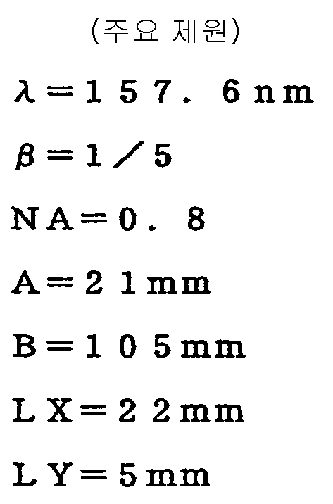
도 2는 본 발명의 각 실시예에 관한 반사굴절광학계를 투영광학계로서 구비한 노광장치의 전체 구성을 개략적으로 도시한 도면이다. 또한, 도 2에서 투영광학계(PL)를 구성하는 반사굴절광학계의 기준 광축(AX)에 평행으로 Z축을, 광축(AX)에 수직인 내부면에서 도 2의 지면에 평행으로 Y축을, 지면에 수직으로 X축을 설정 하고 있다.FIG. 2 is a diagram schematically showing the overall configuration of an exposure apparatus including a reflection refractive optical system according to each embodiment of the present invention as a projection optical system. In addition, in FIG. 2, the Z axis is parallel to the reference optical axis AX of the reflection refractive optical system constituting the projection optical system PL, and the Y axis is parallel to the ground of FIG. 2 from the inner surface perpendicular to the optical axis AX. The X axis is set vertically.
도시한 노광장치는 자외영역의 조명광을 공급하기 위한 광원(100)으로서 F2레이저 광원(발진중심파장 157.6㎚)을 구비하고 있다. 광원(100)으로부터 사출된 광은 조명광학계(IL)를 통하여, 소정의 패턴이 형성된 레티클(마스크)(R)을 균일하게 조명한다. 또한, 광원(100)과 조명광학계(IL)의 사이의 광로는 케이싱(도시하지 않음)에서 밀봉되어 있고, 광원(100)으로부터 조명광학계(IL) 중의 가장 레티클측의 광학부재까지의 공간은 노광광의 흡수율이 낮은 기체인 헬륨가스나 질소 등의 불활성 가스로 치환되어 있거나, 또는 거의 진공상태로 유지되어 있다.The illustrated exposure apparatus includes a F 2 laser light source (oscillation center wavelength 157.6 nm) as a
레티클(R)은 레티클 홀더(RH)를 통하여, 레티클 스테이지(RS)상에서 XY평면에 평행으로 유지되어 있다. 레티클(R)에는 전사해야할 패턴이 형성되어 있고, 패턴 영역 전체 중 X방향을 따라서 단변을 갖고 또한 Y방향을 따라서 단변을 갖는 직사각형 형상의 패턴 영역이 조명된다. 레티클 스테이지(RS)는 도시를 생략한 구동계의 작용에 의해 레티클면(즉 XY평면)을 따라서 이차원적으로 이동 가능하고, 그 위치 좌표는 레티클 이동경(RM)을 사용한 간섭계(RIF)에 의해 계측되고 위치제어되도록 구성되어 있다.The reticle R is held parallel to the XY plane on the reticle stage RS via the reticle holder RH. A pattern to be transferred is formed in the reticle R, and a rectangular pattern region having a short side along the X direction and a short side along the Y direction is illuminated among the entire pattern regions. The reticle stage RS can be moved two-dimensionally along the reticle plane (i.e., XY plane) by the action of a drive system not shown, and its position coordinates are measured by an interferometer RIF using a reticle moving mirror RM. It is configured to control the position.
레티클(R)에 형성된 패턴으로부터의 광은 반사굴절형의 투영광학계(PL)를 통하여, 감광성 기판인 웨이퍼(W)상에 레티클 패턴상을 형성한다. 웨이퍼(W)는 웨이퍼 테이블(웨이퍼 홀더)(WT)을 통하여, 웨이퍼 스테이지(WS)상에서 XY평면에 평행으로 유지되어 있다. 그리고, 레티클(R)상에서의 직사각형 형상의 조명영역에 광 학적으로 대응하도록, 웨이퍼(W)상에서는 X방향을 따라서 장변을 갖고 또한 Y방향을 따라서 단변을 갖는 직사각형 형상의 노광영역에 패턴상이 형성된다. 웨이퍼 스테이지(WS)는 도시를 생략한 구동계의 작용에 의해 웨이퍼면(즉 XY평면)을 따라서 이차원적으로 이동 가능하고, 그 위치 좌표는 웨이퍼 이동경(WM)을 사용한 간섭계(WIF)에 의해 계측되고 위치 제어되도록 구성되어 있다.Light from the pattern formed in the reticle R forms a reticle pattern image on the wafer W, which is a photosensitive substrate, through the reflection-refractive projection optical system PL. The wafer W is held parallel to the XY plane on the wafer stage WS through the wafer table (wafer holder) WT. On the wafer W, a pattern is formed in a rectangular exposure area having a long side along the X direction and a short side along the Y direction so as to optically correspond to the rectangular illumination area on the reticle R. . The wafer stage WS can be moved two-dimensionally along the wafer surface (i.e., XY plane) by the action of a driving system (not shown), and the position coordinates thereof are measured by an interferometer WIF using a wafer moving diameter WM. It is configured to be position controlled.
도 3은 웨이퍼상에 형성되는 직사각형 형상의 노광영역(즉 실효노광영역)과 기준 광축의 위치 관계를 도시한 도면이다. 도 3에 도시한 바와 같이 각 실시예(단, 제 6 실시예 제외)에서는 기준 광축(AX)을 중심으로 한 반경(A)(최대 상 높이에 대응)을 갖는 원형의 영역(이미지 서클)(IF) 내에서 기준 광축(AX)로부터 -Y방향으로 편심한 위치에 소망의 크기를 갖는 직사각형 형상의 실효노광영역(ER)이 설정되어 있다. 여기에서, 실효노광영역(ER)의 X방향의 길이는 LX이고, 그 Y방향의 길이는 LY이다.3 is a diagram showing the positional relationship between a rectangular exposure area (that is, an effective exposure area) and a reference optical axis formed on a wafer. As shown in Fig. 3, in each embodiment (except the sixth embodiment), a circular area (image circle) having a radius A (corresponding to the maximum image height) around the reference optical axis AX ( In the IF), a rectangular effective effective exposure area ER having a desired size is set at a position eccentric from the reference optical axis AX in the -Y direction. Here, the length of the effective exposure area ER in the X direction is LX, and the length of the Y direction is LY.
따라서, 도 1에 도시한 바와 같이 레티클(R)상에서는 기준 광축(AX)으로부터 +Y방향으로 편심한 위치에 실효노광영역(ER)에 대응한 크기 및 형상을 갖는 직사각형 형상의 조명영역(IR)이 형성된다. 즉, 기준 광축(AX)을 중심으로 한 반경(B)(최대 물체높이에 대응)을 갖는 원형 영역내에서 기준 광축(AX)으로부터 +Y방향으로 편심한 위치에 소망의 크기를 갖는 직사각형 형상의 조명영역(IR)이 설정되어 있다.Accordingly, as shown in FIG. 1, on the reticle R, a rectangular illumination area IR having a size and shape corresponding to the effective exposure area ER at a position eccentric to the + Y direction from the reference optical axis AX. Is formed. That is, a rectangular shape having a desired size at a position eccentric to the + Y direction from the reference optical axis AX within a circular area having a radius B (corresponding to the maximum object height) around the reference optical axis AX. Illumination area IR is set.
또한, 도시한 노광장치에서는 투영광학계(PL)를 구성하는 광학부재 중 가장 레티클측에 배치된 광학부재(각 실시예에서는 렌즈(L11))와 가장 웨이퍼측에 배치 된 광학부재(제 1 및 제 2 실시예에서는 렌즈(L38), 제 3 실시예에서는 렌즈(L312), 제 4 실시예에서는 렌즈(L39), 제 5, 제 6 및 제 9 실시예에서는 렌즈(L315), 제 7 및 제 8 실시예에서는 렌즈(L317))의 사이에서 투영광학계(PL)의 내부가 기밀상태를 유지하도록 구성되고, 투영광학계(PL)의 내부의 기체는 헬륨가스나 질소 등의 불활성 가스로 치환되어 있거나, 또는 거의 진공상태로 유지되어 있다.In the illustrated exposure apparatus, among the optical members constituting the projection optical system PL, the optical member disposed on the most reticle side (lens L11 in each embodiment) and the optical member disposed on the wafer side most (first and first). The lens L38 in the second embodiment, the lens L312 in the third embodiment, the lens L39 in the fourth embodiment, the lens L315 in the fifth, sixth and ninth embodiments, the seventh and eighth embodiments. In the embodiment, the interior of the projection optical system PL is maintained in the airtight state between the lenses L317, and the gas inside the projection optical system PL is replaced with an inert gas such as helium gas or nitrogen, Or it is kept almost in vacuum.
또한, 조명광학계(IL)와 투영광학계(PL) 사이의 좁은 광로에는 레티클(R) 및 레티클 스테이지(RS)등이 배치되어 있지만, 레티클(R) 및 레티클 스테이지(RS) 등을 밀봉 포위하는 케이싱(도시하지 않음)의 내부에 질소나 헬륨가스 등의 불활성 가스가 충전되어 있거나, 또는 거의 진공상태로 유지되어 있다.In addition, although a reticle R and a reticle stage RS are disposed in a narrow optical path between the illumination optical system IL and the projection optical system PL, a casing which encloses the reticle R and the reticle stage RS and the like. (Not shown) is filled with an inert gas such as nitrogen or helium gas, or maintained in a substantially vacuum state.
또한, 투영광학계(PL)와 웨이퍼(W) 사이의 좁은 광로에는 웨이퍼(W) 및 웨이퍼 스테이지(WS) 등이 배치되어 있지만, 웨이퍼(W) 및 웨이퍼 스테이지(WS) 등을 밀봉 포위하는 케이싱(도시하지 않음)의 내부에 질소나 헬륨가스 등의 불활성 가스가 충전되어 있거나, 또는 거의 진공상태로 유지되어 있다. 이와 같이, 광원(100)으로부터 웨이퍼(W)까지의 광로 전체에 걸쳐, 노광광이 거의 흡수되지 않는 분위기가 형성되어 있다.In addition, although the wafer W, the wafer stage WS, and the like are disposed in the narrow optical path between the projection optical system PL and the wafer W, a casing (not shown) encapsulating the wafer W, the wafer stage WS, or the like is provided. (Not shown) is filled with an inert gas such as nitrogen or helium gas, or maintained in a nearly vacuum state. Thus, the atmosphere in which exposure light is hardly absorbed is formed over the whole optical path from the
상술한 바와 같이 투영광학계(PL)에 의해 규정되는 레티클(R)상의 조명영역 및 웨이퍼(W)상의 노광영역(즉 실효노광영역(ER))은 Y방향을 따라서 단변을 갖는 직사각형 형상이다. 따라서, 구동계 및 간섭계(RIF, WIF) 등을 사용하여 레티클(R) 및 웨이퍼(W)의 위치제어를 실시하면서, 직사각형 형상의 노광영역 및 조명영역의 단변방향 즉 Y방향을 따라서 레티클 스테이지(RS)와 웨이퍼 스테이지(WS)를, 더 나아가서는 레티클(R)과 웨이퍼(W)를 반대 방향으로 (즉 반대 방면으로) 동기적으로 이동(주사)시킴으로써 웨이퍼(W)상에는 노광영역의 장변에 동등한 폭을 갖고 또한 웨이퍼(W) 주사량(이동량)에 맞는 길이를 갖는 영역에 대해서 레티클 패턴이 주사 노광된다.As described above, the illumination area on the reticle R and the exposure area on the wafer W (that is, the effective exposure area ER) defined by the projection optical system PL have a rectangular shape with short sides along the Y direction. Accordingly, the reticle stage RS is performed along the short sides of the rectangular exposure area and the illumination area, that is, the Y direction, while controlling the position of the reticle R and the wafer W using the drive system and the interferometer RIF, WIF, or the like. ) And the wafer stage WS, further, by synchronously moving (scanning) the reticle R and the wafer W in the opposite direction (that is, in the opposite direction), which is equivalent to the long side of the exposure area on the wafer W. The reticle pattern is scanned and exposed to an area having a width and having a length corresponding to the wafer W scanning amount (movement amount).
각 실시예에서 본 발명의 반사굴절광학계로 이루어진 투영광학계(PL)는 제 1 면에 배치된 레티클(R) 패턴의 제 1 중간상을 형성하기 위한 반사굴절형의 제 1 결상광학계(G1)와, 제 1 결상광학계(G1)를 통한 광에 기초하여 레티클(R)의 패턴의 제 2 중간상을 형성하기 위한 반사굴절형의 제 2 결상광학계(G2)와, 제 2 결상광학계(G2)를 통한 광에 기초하여 제 2 면에 배치된 웨이퍼(W)상에 레티클 패턴의 최종상(레티클 패턴의 축소상)을 형성하기 위한 굴절형 제 3 결상광학계(G3)를 구비하고 있다. In each embodiment, the projection optical system PL including the reflective refractive optical system of the present invention includes a first refractive optical system G1 having a refractive index type for forming the first intermediate image of the reticle R pattern disposed on the first surface; A second refractive optical system G2 of reflection type for forming a second intermediate image of the pattern of the reticle R based on the light through the first imaging optical system G1, and the light through the second imaging optical system G2. And a refractive-type third imaging optical system G3 for forming the final image (reduced image of the reticle pattern) of the reticle pattern on the wafer W arranged on the second surface.
또한, 각 실시예에서 제 1 결상광학계(G1), 제 2 결상광학계(G2) 및 제 3 결상광학계(G3)를 구성하는 모든 광학부재가 단일한 직선형상 광축(AX)을 따라서 배치되어 있다. 또한, 제 1 결상광학계(G1)와 제 2 결상광학계(G2) 사이의 광로중에는 제 1 필드렌즈가 배치되어 있다. 또한, 제 2 결상광학계(G2)와 제 3 결상광학계(G3) 사이의 광로중에는 제 2 필드렌즈가 배치되어 있다. 또한, 기준 광축(AX)은 중력방향(즉 연직방향)을 따라서 위치되어 있다. 그 결과, 레티클(R) 및 웨이퍼(W)는 중력방향과 직교하는 면 즉 수평면을 따라서 서로 평행으로 배치되어 있다. 또한, 투영광학계(PL)를 구성하는 모든 광학부재(렌즈 및 반사경)도, 기준광 축(AX)상에서 수평면을 따라서 배치되어 있다.In each embodiment, all the optical members constituting the first imaging optical system G1, the second imaging optical system G2, and the third imaging optical system G3 are arranged along a single linear optical axis AX. Further, a first field lens is disposed in the optical path between the first imaging optical system G1 and the second imaging optical system G2. Further, a second field lens is disposed in the optical path between the second imaging optical system G2 and the third imaging optical system G3. In addition, the reference optical axis AX is located along the gravity direction (ie, the vertical direction). As a result, the reticle R and the wafer W are arranged in parallel with each other along a plane orthogonal to the gravity direction, that is, a horizontal plane. Moreover, all the optical members (lens and reflecting mirror) which comprise the projection optical system PL are also arrange | positioned along the horizontal plane on the reference optical axis AX.
각 실시예에서 투영광학계(PL)를 구성하는 모든 굴절광학부재(렌즈성분)에는 형석(CaF2결정)을 사용하고 있다. 또한, 노광광인 F2레이저광의 발진중심파장은 157.6㎚이고, 157.6㎚ 부근에서 CaF2의 굴절율은 +1pm의 파장변화당 -2×10⁻⁶의 비율로 변화되고, -1pm의 파장변화당 +2×10⁻⁶의 비율로 변화된다. 다시 말하면, 157.6㎚부근에서 CaF2의 굴절률의 분산(dn/dλ)은 2×10⁻⁶/pm이다.In each embodiment, fluorite (CaF 2 crystal) is used for all refractive optical members (lens components) constituting the projection optical system PL. In addition, the oscillation center wavelength of the F 2 laser light, which is exposure light, is 157.6 nm, and the refractive index of CaF 2 is changed at a ratio of -2 × 10 -6 per wavelength change of +1 pm, and + per wavelength change of -1 pm at around 157.6 nm. The ratio is changed to 2 × 10 −6 . In other words, the dispersion (dn / dλ) of the refractive index of CaF 2 in the vicinity of 157.6 nm is 2 × 10 −6 / pm.
따라서, 각 실시예에서 중심파장 157.6㎚에 대한 CaF2의 굴절율은 1.560000이다. 그리고, 제 1 실시예, 제 2 실시예 및 제 4 실시예에서는 157.6㎚+0.5pm=157.6005㎚에 대한 CaF2의 굴절율은 1.559999이고 157.6㎚-0.5pm=157.5995㎚에 대한 CaF2의 굴절율은 1.560001이다. 또한, 제 3 실시예, 제 5 실시예 및 제 6 실시예에서는 157.6㎚+0.3pm=157.6003㎚에 대한 CaF2의 굴절율은 1.5599994이고, 157.6㎚-0.3pm=157.5997㎚에 대한 CaF2의 굴절율은 1.5600006이다. 또한, 제 7 실시예∼제 9 실시예에서는 157.6㎚+0.4pm=157.6004㎚에 대한 CaF2의 굴절율은 1.5599992이고 157.6㎚-0.4pm=157.5996㎚에 대한 CaF2의 굴절율은 1.5600008이다.Therefore, the refractive index of CaF 2 with respect to the center wavelength of 157.6 nm in each example is 1.560000. And, in the first embodiment, second embodiment and the fourth embodiment, 157.6㎚ + 0.5pm = index of refraction of CaF 2 is about 1.559999 and 157.6005㎚ 157.6㎚-0.5pm = index of refraction of CaF 2 is about 157.5995㎚ 1.560001 to be. Further, in the third, fifth and sixth examples, the refractive index of CaF 2 for 157.6 nm + 0.3 pm = 157.6003 nm is 1.5599994, and the refractive index of CaF 2 for 157.6 nm-0.3 pm = 157.5997 nm. 1.5600006. In addition, the seventh embodiment to ninth embodiment, the index of refraction of CaF 2 on the index of refraction of CaF 2 is 1.5599992 and 157.6㎚-0.4pm = 157.5996㎚ for 157.6㎚ + 0.4pm = 157.6004㎚ is 1.5600008.
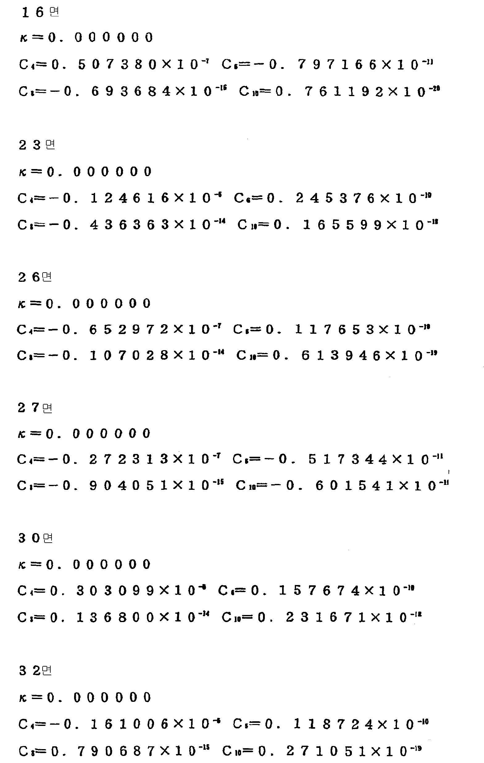
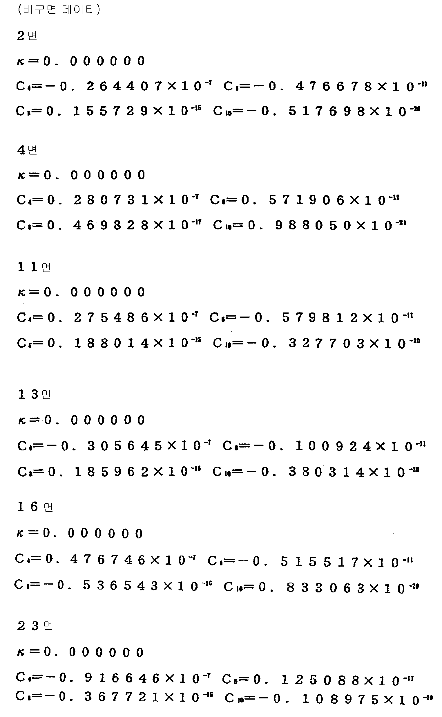
또한, 각 실시예에서 비(非)구면은 광축에 수직인 방향의 높이를 y로 하고, 비구면의 정점에서의 접평면으로부터 높이 y에서의 비구면상의 위치까지의 광축을 따른 거리(새그량)를 z로 하고, 정점곡률반경을 r로 하고, 원추계수를 к로 하고, n차의 비구면 계수를 Cn으로 했을 때 이하의 수식으로 나타난다.In each embodiment, the aspherical surface has a height in a direction perpendicular to the optical axis y, and a distance (sag amount) along the optical axis from the tangent plane at the apex of the aspherical surface to the aspherical position at the height y is z. When the peak curvature radius is r, the cone coefficient is k, and the n-th aspherical coefficient is Cn, it is expressed by the following formula.
![]()
![]()
각 실시예에서 비구면 형상으로 형성된 렌즈면에는 면 번호의 우측에 *표를 붙이고 있다.In each embodiment, the lens surface formed in aspherical shape is denoted by * mark on the right side of the surface number.
(제 1 실시예)(First embodiment)
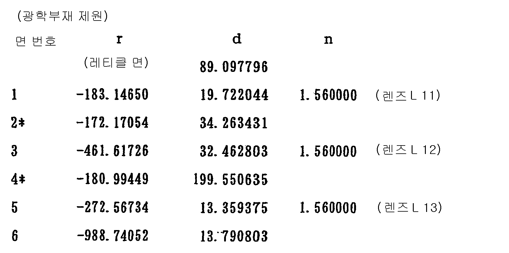
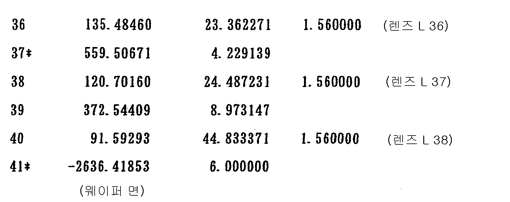
도 4는 제 1 실시예에 관한 반사굴절광학계(투영광학계(PL))의 렌즈 구성을 도시한 도면이다. 도 4의 반사굴절광학계에서 제 1 결상광학계(G1)는 레티클측부터 차례로 웨이퍼측에 비구면 형상의 볼록면을 향한 정(正) 메니스커스렌즈(L11)와, 웨이퍼측에 비구면 형상의 볼록면을 향한 정 메니스커스렌즈(L12)와, 웨이퍼측에 평면에 가까운 오목면을 향한 오목면 반사경(M11)과, 레티클측에 오목면을 향한 부(負) 메니스커스렌즈(L13)와, 레티클측에 오목면을 향한 오목면 반사경(M12)으로 구성되어 있다.FIG. 4 is a diagram showing a lens configuration of a reflective refractive optical system (projection optical system PL) according to the first embodiment. In the reflective refractive optical system of Fig. 4, the first imaging optical system G1 has a positive meniscus lens L11 facing the aspherical convex surface from the reticle side to the wafer side, and an aspheric convex surface on the wafer side. A positive meniscus lens L12 facing the surface, a concave reflecting mirror M11 facing a plane near the plane on the wafer side, a negative meniscus lens L13 facing a concave surface on the reticle side, It is comprised by the concave reflecting mirror M12 toward the concave surface at the reticle side.
또한, 제 2 결상광학계(G2)는 레티클측부터 차례로, 웨이퍼측에 오목면을 향한 오목면 반사경(M21)과, 레티클측에 볼록면을 향한 부 메니스커스렌즈(L21)와, 레티클측에 평면에 가까운 오목면을 향한 오목면 반사경(M22)으로 구성되어 있다.The second imaging optical system G2 has a concave reflecting mirror M21 facing the concave surface on the wafer side, a sub meniscus lens L21 facing the convex surface on the reticle side, and a reticle side from the reticle side. It is comprised by the concave reflecting mirror M22 toward the concave surface near a plane.
또한, 제 3 결상광학계(G3)는 레티클측부터 차례로, 웨이퍼측에 비구면형상의 볼록면을 향한 부 메니스커스렌즈(L31)와, 레티클측에 비구면 형상의 볼록면을 향한 부 메니스커스렌즈(L32)와, 웨이퍼측에 비구면 형상의 오목면을 향한 정 메니스커스렌즈(L33)와, 개구조리개(AS)와, 레티클측에 비구면 형상의 오목면을 향한 정 메니스커스렌즈(L34)와, 웨이퍼측에 비구면 형상의 오목면을 향한 정 메니스커스렌즈(L35)와, 웨이퍼측에 비구면 형상의 오목면을 향한 정 메니스커스렌즈(L36)와, 양(兩)볼록렌즈(L37)와, 웨이퍼측에 비구면 형상의 볼록면을 향한 양볼록렌즈(L38)로 구성되어 있다.In addition, the third imaging optical system G3 has a sub meniscus lens L31 facing the convex surface of the aspherical surface on the wafer side from the reticle side, and a sub meniscus lens facing the convex surface of the aspherical surface on the reticle side. (L32), positive meniscus lens L33 facing the aspherical concave surface on the wafer side, aperture stop AS, and positive meniscus lens L34 facing the aspherical concave surface on the reticle side And a positive meniscus lens L35 facing the aspherical concave surface on the wafer side, a positive meniscus lens L36 facing the aspherical concave surface on the wafer side, and a biconvex lens L37. ) And a biconvex lens L38 facing the convex surface of the aspherical surface on the wafer side.
또한, 제 1 결상광학계(G1)와 제 2 결상광학계(G2) 사이의 광로중에는 레티클측부터 차례로, 레티클측에 비구면 형상의 오목면을 향한 정 메니스커스렌즈(L41)와, 레티클측에 비구면 형상의 볼록면을 향한 양볼록렌즈(L42)와, 웨이퍼측에 비구면 형상의 오목면을 향한 정 메니스커스렌즈(L43)로 구성된 제 1 필드렌즈가 배치되어 있다. 또한, 제 2 결상광학계(G2)와 제 3 결상광학계(G3) 사이의 광로중에는 레티클측에 비구면 형상의 볼록면을 향한 양볼록렌즈(L51)로 구성된 제 2 필드렌즈가 배치되어 있다.In addition, in the optical path between the first imaging optical system G1 and the second imaging optical system G2, the positive meniscus lens L41 faces the aspherical concave surface on the reticle side from the reticle side, and the aspherical surface on the reticle side. A first field lens composed of a biconvex lens L42 facing the convex surface in the shape and a positive meniscus lens L43 facing the concave surface in the aspherical shape are disposed on the wafer side. Further, in the optical path between the second imaging optical system G2 and the third imaging optical system G3, a second field lens composed of a biconvex lens L51 facing an aspherical convex surface is arranged on the reticle side.
따라서, 제 1 실시예에서는 레티클(R)로부터의 광이 정 메니스커스렌즈(L11), 정 메니스커스렌즈(L12) 및 부 메니스커스렌즈(L13)를 통하여, 오목면 반사경(M12)에 입사한다. 오목면 반사경(M12)에서 반사된 광은 부 메니스커스렌즈(L13)를 통하여 오목면 반사경(M11)에서 반사된 후, 제 1 필드렌즈(L41∼L43) 중에 레티클 패턴의 제 1 중간상을 형성한다.Therefore, in the first embodiment, the light from the reticle R passes through the positive meniscus lens L11, the positive meniscus lens L12 and the secondary meniscus lens L13, and the concave reflecting mirror M12. Enters into. The light reflected by the concave reflector M12 is reflected by the concave reflector M11 through the sub meniscus lens L13, and then forms a first intermediate image of the reticle pattern in the first field lenses L41 to L43. do.
제 1 필드렌즈(L41∼L43) 중에 형성된 제 1 중간상으로부터의 광은 오목면 반사경(M22)에서 반사되고, 부 메니스커스렌즈(L21)를 통하여 오목면 반사경(M21) 에서 반사된 후, 부 메니스커스렌즈(L21)를 통하여 제 2 필드렌즈(L51)의 근방에 레티클 패턴의 제 2 중간상을 형성한다. 제 2 필드렌즈(L51)의 근방에 형성된 제 2 중간상으로부터의 광은 제 3 결상광학계(G3)를 구성하는 각 렌즈(L31∼L38)를 통하여, 웨이퍼(W)상에 레티클 패턴의 최종상을 형성한다.Light from the first intermediate image formed in the first field lenses L41 to L43 is reflected by the concave reflector M22, and is reflected by the concave reflector M21 through the sub meniscus lens L21, and then is negative. A second intermediate image of the reticle pattern is formed in the vicinity of the second field lens L51 through the meniscus lens L21. Light from the second intermediate image formed near the second field lens L51 forms the final image of the reticle pattern on the wafer W through the respective lenses L31 to L38 constituting the third imaging optical system G3. do.
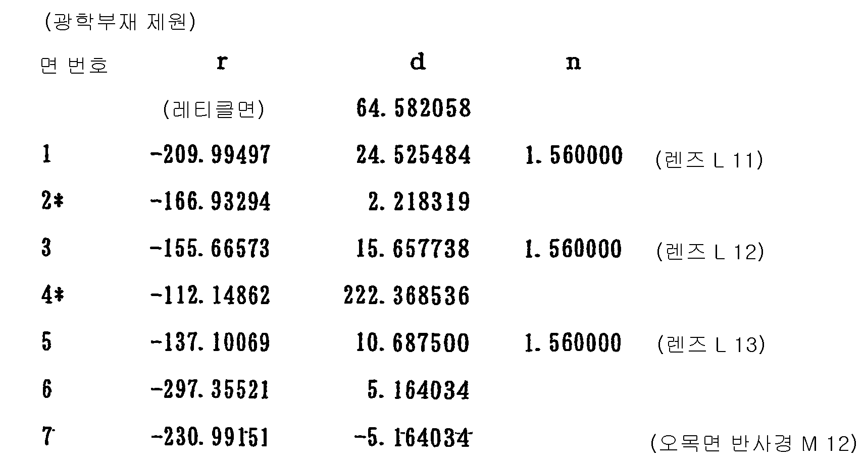
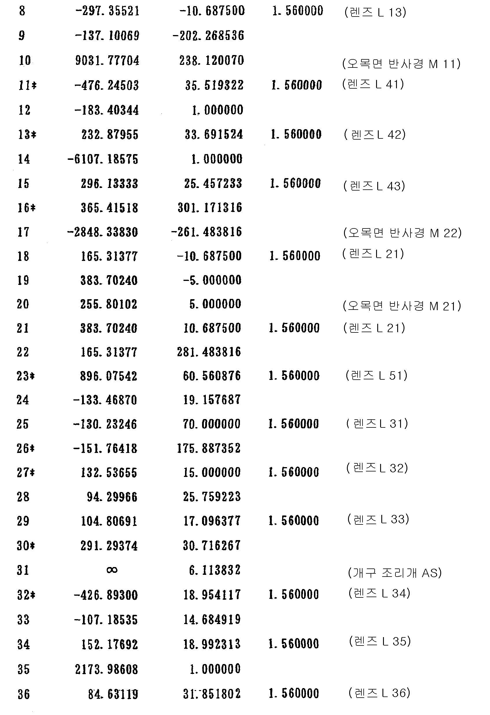
다음의 표 1에, 제 1 실시예의 반사굴절광학계의 제원의 값을 든다. 표 1의 주요제원에서 λ은 노광광의 중심파장을, β는 투영배율(전체계의 결상배율)을, NA는 상(像)측(웨이퍼측) 개구수를, A는 웨이퍼(W)상에서의 이미지 서클(IF)의 반경 즉 최대 상 높이를, B는 최대 상 높이(A)에 대응하는 최대 물체 높이를, LX는 실효노광영역(ER)의 X방향을 따른 크기(장변의 크기)를, LY는 실효노광영역(ER)의 Y방향을 따른 크기(단변의 크기)를 각각 나타내고 있다.Table 1 below shows the values of the specifications of the reflective refractive optical system of the first embodiment. In the main specifications of Table 1, λ is the center wavelength of the exposure light, β is the projection magnification (image-forming magnification of the whole system), NA is the numerical aperture on the image side (wafer side), and A is on the wafer W. The radius of the image circle IF, that is, the maximum image height, B is the maximum object height corresponding to the maximum image height A, LX is the size along the X direction of the effective exposure area ER (the size of the long side), LY represents the magnitude | size (size of a short side) along the Y direction of the effective exposure area ER, respectively.
또한, 표 1의 광학부재 제원에서 제 1 컬럼의 면 번호는 레티클측부터의 면의 순서를, 제 2 컬럼의 r은 각 면의 곡률반경(비구면의 경우에는 정점곡율반경:㎜)을, 제 3 컬럼의 d는 각 면의 축상 간격 즉 면간격(㎜)을, 제 4 컬럼의 n은 중심파장에 대한 굴절율을 각각 나타내고 있다. 또한, 면간격(d)은 반사될 때마다 그 부호를 바꾸는 것으로 한다. 따라서, 면간격(d)의 부호는 오목면 반사경(M12)으로부터 오목면 반사경(M11)으로의 광로 중 및 오목면 반사경(M22)으로부터 오목면 반사경(M21)으로의 광로 중에서는 부로 하고, 그 밖의 광로중에서는 정으로 하고 있다. 또한, 광의 입사방향에 관계없이, 레티클측을 향하여 볼록면의 곡률반경을 정으로 하고, 레티클측을 향하여 오목면의 곡률반경을 부로 하고 있다. In the optical member specifications of Table 1, the surface number of the first column is the order of the surface from the reticle side, and the r of the second column is the radius of curvature of each surface (vertical radius of curvature: mm). D in each of the three columns represents the axial spacing of each surface, that is, the surface spacing (mm), and n in the fourth column represents the refractive index with respect to the center wavelength. It is to be noted that the plane interval d changes its sign every time it is reflected. Therefore, the sign of the surface interval d is negative in the optical path from the concave reflector M12 to the concave reflector M11 and in the optical path from the concave reflector M22 to the concave reflector M21, It is made into the middle in the outside light path. Regardless of the direction of incidence of light, the radius of curvature of the convex surface is set toward the reticle side, and the radius of curvature of the concave surface is made negative toward the reticle side.
(표 1)Table 1


도 5는 제 1 실시예에 관한 반사굴절광학계의 가로수차를 도시한 도면이다. 수차도에서 Y는 상 높이(㎜)를 나타내고 있다. 수차도로부터 밝혀진 바와 같이, 제 1 실시예에서는 파장폭이 157.6㎚±0.5pm의 노광광에 대해서 색수차가 양호하게 보정되어 있는 것을 알 수 있다. 또한, 구면수차, 코머수차, 비점수차, 디스토션(왜곡수차)이 거의 무수차에 가까운 상태까지 양호하게 보정되고, 우수한 결상성능을 갖는 것을 확인하고 있다.Fig. 5 is a diagram showing the horizontal aberration of the reflection refractive optical system according to the first embodiment. In the aberration diagram, Y represents the image height (mm). As is clear from the aberration diagram, it can be seen that in the first embodiment, chromatic aberration is well corrected for exposure light having a wavelength width of 157.6 nm ± 0.5 pm. In addition, it has been confirmed that spherical aberration, comer aberration, astigmatism, and distortion (distortion aberration) are well corrected to almost an aberration, and have excellent imaging performance.
(제 2 실시예)(Second embodiment)
도 6은 제 2 실시예에 관한 반사굴절광학계(투영광학계(PL))의 렌즈 구성을 도시한 도면이다. 도 6의 반사굴절광학계에서 제 1 결상광학계(G1)는 레티클측부터 차례로, 웨이퍼측에 비구면 형상의 볼록면을 향한 정 메니스커스렌즈(L11)와, 웨이퍼측에 비구면 형상의 볼록면을 향한 정 메니스커스렌즈(L12)와, 웨이퍼측에 평면에 가까운 오목면을 향한 오목면 반사경(M11)과, 레티클측에 오목면을 향한 부 메니스커스렌즈(L13)와, 레티클측에 오목면을 향한 오목면 반사경(M12)으로 구성되 어 있다.FIG. 6 is a diagram showing a lens configuration of a reflective refractive optical system (projection optical system PL) according to the second embodiment. In the reflective refractive optical system of Fig. 6, the first imaging optical system G1 is sequentially directed from the reticle side to the positive meniscus lens L11 toward the aspherical convex surface on the wafer side, and toward the aspherical convex surface on the wafer side. The positive meniscus lens L12, the concave reflecting mirror M11 toward the concave surface close to the plane on the wafer side, the sub meniscus lens L13 facing the concave surface on the reticle side, and the concave surface on the reticle side It is composed of a concave reflector M12 facing toward.
또한, 제 2 결상광학계(G2)는 레티클측부터 차례로, 웨이퍼측에 오목면을 향한 오목면 반사경(M21)과, 레티클측에 볼록면을 향한 부 메니스커스렌즈(L21)와, 레티클측에 평면에 가까운 오목면을 향한 오목면 반사경(M22)으로 구성되어 있다.The second imaging optical system G2 has a concave reflecting mirror M21 facing the concave surface on the wafer side, a sub meniscus lens L21 facing the convex surface on the reticle side, and a reticle side from the reticle side. It is comprised by the concave reflecting mirror M22 toward the concave surface near a plane.
또한, 제 3 결상광학계(G3)는 레티클측부터 차례로, 웨이퍼측에 비구면 형상의 볼록면을 향한 부 메니스커스렌즈(L31)와, 레티클측에 비구면 형상의 볼록면을 향한 부 메니스커스렌즈(L32)와, 웨이퍼측에 비구면 형상의 볼록면을 향한 양볼록렌즈(L33)와, 개구 조리개(AS)와, 레티클측에 비구면 형상의 볼록면을 향한 양볼록렌즈(L34)와, 레티클측에 볼록면을 향한 정 메니스커스렌즈(L35)와, 웨이퍼측에 비구면 형상의 오목면을 향한 정 메니스커스렌즈(L36)와, 레티클측에 볼록면을 향한 정 메니스커스렌즈(L37)와, 웨이퍼측에 비구면 형상의 볼록면을 향한 양볼록렌즈(L38)로 구성되어 있다.In addition, the third imaging optical system G3 has a sub meniscus lens L31 facing the convex surface of the aspherical surface on the wafer side from the reticle side, and a sub meniscus lens facing the convex surface of the aspherical surface on the reticle side. (L32), biconvex lens L33 facing the aspherical convex surface on the wafer side, aperture diaphragm AS, biconvex lens L34 facing the aspheric convex surface on the reticle side, and the reticle side Positive meniscus lens L35 facing the convex surface, positive meniscus lens L36 facing the aspherical concave surface on the wafer side, and positive meniscus lens L37 facing the convex surface on the reticle side. And a biconvex lens L38 facing an aspherical convex surface on the wafer side.
또한, 제 1 결상광학계(G1)와 제 2 결상광학계(G2) 사이의 광로중에는 레티클측부터 차례로, 레티클측에 비구면 형상의 오목면을 향한 정 메니스커스렌즈(L41)와, 레티클측에 비구면 형상의 볼록면을 향한 정 메니스커스렌즈(L42)와, 웨이퍼측에 비구면 형상의 오목면을 향한 정 메니스커스렌즈(L43)로 구성된 제 1 필드렌즈가 배치되어 있다. 또한, 제 2 결상광학계(G2)와 제 3 결상광학계(G3) 사이의 광로중에는 레티클측에 비구면 형상의 볼록면을 향한 양볼록렌즈(L51)로 구성된 제 2 필드렌즈가 배치되어 있다.In addition, in the optical path between the first imaging optical system G1 and the second imaging optical system G2, the positive meniscus lens L41 faces the concave surface of the aspherical shape on the reticle side from the reticle side, and the aspherical surface on the reticle side. A first field lens composed of the positive meniscus lens L42 facing the convex surface of the shape and the positive meniscus lens L43 facing the concave surface of the aspherical shape is disposed on the wafer side. Further, in the optical path between the second imaging optical system G2 and the third imaging optical system G3, a second field lens composed of a biconvex lens L51 facing an aspherical convex surface is arranged on the reticle side.
따라서, 제 2 실시예에서는 레티클(R)로부터의 광이 정 메니스커스렌즈(L11), 정 메니스커스렌즈(L12) 및 부 메니스커스렌즈(L13)를 통하여, 오목면 반사경(M12)에 입사한다. 오목면 반사경(M12)에서 반사된 광은 부 메니스커스렌즈(L13)를 통하여, 오목면 반사경(M11)에서 반사된 후, 제 1 필드렌즈(L41~L43) 중에 레티클 패턴의 제 1 중간상을 형성한다. Therefore, in the second embodiment, the light from the reticle R passes through the positive meniscus lens L11, the positive meniscus lens L12 and the secondary meniscus lens L13, and the concave reflecting mirror M12. Enters into. The light reflected by the concave reflector M12 is reflected by the concave reflector M11 through the sub meniscus lens L13, and then the first intermediate image of the reticle pattern is formed in the first field lenses L41 to L43. Form.
제 1 필드렌즈(L41~L43) 중에 형성된 제 1 중간상으로부터의 광은 오목면 반사경(M22)에서 반사되고, 부 메니스커스렌즈(L21)를 통하여 오목면 반사경(M21)에서 반사된 후, 부 메니스커스렌즈(L21)를 통하여 제 2 필드렌즈(L51)의 근방에 레티클 패턴의 제 2 중간상을 형성한다. 제 2 필드렌즈(L51) 근방에 형성된 제 2 중간상으로부터의 광은 제 3 결상광학계(G3)를 구성하는 각 렌즈(L31~L38)를 통하여 웨이퍼(W)상에 레티클 패턴의 최종상을 형성한다.The light from the first intermediate image formed in the first field lenses L41 to L43 is reflected by the concave reflector M22 and reflected by the concave reflector M21 through the sub meniscus lens L21, and then A second intermediate image of the reticle pattern is formed in the vicinity of the second field lens L51 through the meniscus lens L21. Light from the second intermediate image formed near the second field lens L51 forms the final image of the reticle pattern on the wafer W through the respective lenses L31 to L38 constituting the third imaging optical system G3.
다음의 표 2에, 제 2 실시예의 반사굴절광학계의 제원의 값을 든다. 표 2의 주요제원에서, λ는 노광광의 중심파장을, β는 투영배율(전체계의 결상배율)을, NA는 상측(웨이퍼측) 개구수를, A는 웨이퍼(W)상에서의 이미지 서클(IF)의 반경 즉 최대 상 높이를, B는 최대 상 높이(A)에 대응하는 최대 물체 높이를, LX는 실효노광영역(ER)의 X방향을 따른 크기(장변의 크기)를, LY는 실효노광영역(ER)의 Y방향을 따른 크기(단변의 크기)를 각각 나타내고 있다.Table 2 below shows the values of the specifications of the reflective refractive optical system of the second embodiment. In the main specifications of Table 2, λ is the center wavelength of the exposure light, β is the projection magnification (image-forming magnification of the whole system), NA is the numerical aperture on the image side (wafer side), and A is the image circle on the wafer W ( IF), that is, the maximum image height, B is the maximum object height corresponding to the maximum image height A, LX is the size (length of the long side) along the X direction of the effective exposure area ER, and LY is the effective value. The magnitude | size (short side size) in the Y direction of the exposure area ER is shown, respectively.
또한, 표 2의 광학부재 제원에서 제 1 컬럼의 면 번호는 레티클측부터의 면의 순서를, 제 2 컬럼의 r은 각 면의 곡률반경(비구면의 경우에는 정점곡률반경:㎜)을, 제 3 컬럼의 d는 각 면의 축상 간격 즉 면 간격(㎜)을, 제 4 컬럼의 n은 중심파장에 대한 굴절율을 각각 나타내고 있다. 또한, 면간격(d)은 반사될 때마다 그 부호를 변화시키는 것으로 한다. 따라서, 면간격(d)의 부호는 오목면 반사경(M12)으로부터 오목면 반사경(M11)으로의 광로중 및 오목면 반사경(M22)으로부터 오목면 반사경(M21)으로의 광로중에서는 부로 하고, 그 밖의 광로중에서는 정으로 하고 있다. 또한, 광의 입사방향에 관계없이 레티클측을 향해서 볼록면의 곡률반경을 정으로 하고, 레티클측을 향하여 오목면의 곡률반경을 부로 하고 있다.In the optical member specifications of Table 2, the surface number of the first column is the order of the surfaces from the reticle side, and the r of the second column is the radius of curvature of each surface (vertical radius of curvature: mm). D in each of the three columns represents the axial spacing of each surface, that is, the surface spacing (mm), and n in the fourth column represents the refractive index with respect to the center wavelength. It is to be noted that the plane interval d changes its sign every time it is reflected. Therefore, the sign of the surface interval d is negative in the optical path from the concave reflector M12 to the concave reflector M11 and in the optical path from the concave reflector M22 to the concave reflector M21. It is made into the middle in the outside light path. Further, the radius of curvature of the convex surface is set toward the reticle side regardless of the incident direction of light, and the radius of curvature of the concave surface is made negative toward the reticle side.
(표 2)Table 2


도 7은 제 2 실시예에 관한 반사굴절광학계의 가로수차를 도시한 도면이다. 수차도에서 Y는 상 높이(㎜)를 도시하고 있다. 수차도로부터 밝혀진 바와 같이, 제 2 실시예에서도 제 1 실시예와 동일하게, 파장폭이 157.6㎚±0.5pm의 노광광에 대해서 색수차가 양호하게 보정되어 있는 것을 알 수 있다. 또한, 구면수차, 코머수차, 비점수차, 디스토션(왜곡수차)이 거의 무수차에 가까운 상태까지 양호하게 보정되고, 우수한 결상성능을 갖는 것을 확인하고 있다.Fig. 7 is a diagram showing the horizontal aberration of the reflective refractive optical system according to the second embodiment. Y in the aberration diagram shows the image height in mm. As is clear from the aberration diagram, it can be seen that similarly to the first embodiment, chromatic aberration is well corrected for exposure light having a wavelength width of 157.6 nm ± 0.5 pm, as in the second embodiment. In addition, it has been confirmed that spherical aberration, comer aberration, astigmatism, and distortion (distortion aberration) are well corrected to almost an aberration, and have excellent imaging performance.
(제 3 실시예)(Third embodiment)
도 8은 제 3 실시예에 관한 반사굴절광학계(투영광학계(PL))의 렌즈 구성을 도시한 도면이다. 도 8의 반사굴절광학계에서 제 1 결상광학계(G1)는 레티클측부터 차례로, 양볼록렌즈(L11)와, 웨이퍼측에 평면에 가까운 오목면을 향한 오목면 반사경(M11)과, 레티클측에 오목면을 향한 오목면 반사경(M12)으로 구성되어 있다.FIG. 8 is a diagram showing a lens configuration of a reflective refractive optical system (projection optical system PL) according to the third embodiment. In the reflective refractive optical system of Fig. 8, the first imaging optical system G1 is concave on the reticle side from the reticle side to the biconvex lens L11, the concave reflecting mirror M11 toward the concave surface close to the plane on the wafer side, It is comprised by the concave reflecting mirror M12 toward a surface.
또한, 제 2 결상광학계(G2)는 레티클측부터 차례로, 웨이퍼측에 오목면을 향한 오목면 반사경(M21)과, 레티클측에 오목면을 향한 부 메니스커스렌즈(L21)와, 레티클측에 평면에 가까운 오목면을 향한 오목면 반사경(M22)으로 구성되어 있다.In addition, the second imaging optical system G2 has a concave reflecting mirror M21 facing the concave surface on the wafer side in order from the reticle side, a sub meniscus lens L21 facing the concave surface on the reticle side, and a reticle side. It is comprised by the concave reflecting mirror M22 toward the concave surface near a plane.
또한, 제 3 결상광학계(G3)는 레티클측부터 차례로, 레티클측에 비구면 형상의 오목면을 향한 정 메니스커스렌즈(L31)와, 레티클측에 볼록면을 향한 부 메니스커스렌즈(L32)와, 레티클측에 볼록면을 향한 정 메니스커스렌즈(L33)와, 웨이퍼측에 비구면형상의 오목면을 향한 정 메니스커스렌즈(L34)와, 양볼록렌즈(L35)와, 레티클측에 비구면 형상의 오목면을 향한 부 메니스커스렌즈(L36)와, 개구 조리개(AS)와, 레티클측에 비구면 형상의 오목면을 향한 부 메니스커스렌즈(L37)와, 웨이퍼측에 비구면 형상의 볼록면을 향한 양볼록렌즈(L38)와, 웨이퍼측에 비구면 형상의 오목면을 향한 정 메니스커스렌즈(L39)와, 레티클측에 볼록면을 향한 정 메니스커스렌즈(L310)와, 양오목렌즈(L311)와, 레티클측에 볼록면을 향한 정 메니스커스렌즈(L312)로 구성되어 있다.Further, the third imaging optical system G3 has a positive meniscus lens L31 facing the concave surface of the aspherical surface on the reticle side and a secondary meniscus lens L32 facing the convex surface on the reticle side. On the reticle side, the positive meniscus lens L33 faces the convex surface, the positive meniscus lens L34 faces the aspherical concave surface on the wafer side, the biconvex lens L35 and the reticle side Aspheric shaped meniscus lens L36 facing the concave surface, aperture diaphragm AS, aspheric shaped meniscus lens L37 facing the aspherical concave surface on the reticle side, and aspheric shaped wafers on the wafer side The biconvex lens L38 facing the convex surface, the positive meniscus lens L39 facing the concave surface of the aspherical shape on the wafer side, the positive meniscus lens L310 facing the convex surface on the reticle side, and both It consists of a concave lens L311 and a positive meniscus lens L312 facing the convex surface on the reticle side.
또한, 제 1 결상광학계(G1)와 제 2 결상광학계(G2)사이의 광로중에는 레티클측부터 차례로, 양볼록렌즈(L41)와, 웨이퍼측에 비구면 형상의 볼록면을 향한 양볼록렌즈(L42)로 구성된 제 1 필드렌즈가 배치되어 있다. 또한, 제 2 결상광학계(G2)와 제 3 결상광학계(G3) 사이의 광로중에는 레티클측부터 차례로, 레티클측에 오목면을 향한 정메니스커스렌스(L51)와, 양볼록렌즈(L52)로 구성된 제 2 필드렌즈가 배치되어 있다.Further, in the optical path between the first imaging optical system G1 and the second imaging optical system G2, the biconvex lens L41 and the biconvex lens L42 facing the convex surface of the aspherical surface on the wafer side in turn from the reticle side. A first field lens composed of The optical path between the second imaging optical system G2 and the third imaging optical system G3 includes a static meniscus L51 and a biconvex lens L52, which in turn are concave to the reticle side from the reticle side. The second field lens is arranged.
따라서, 제 3 실시예에서는 레티클(R)로부터의 광이 양볼록렌즈(L11)를 통하여 오목면 반사경(M12)에 입사한다. 오목면 반사경(M12)에서 반사된 광은, 오목면 반사경(M11)에서 반사된 후, 제 1 필드렌즈(L41 및 L42)를 통하여 레티클 패턴의 제 1 중간상을 형성한다.Therefore, in the third embodiment, light from the reticle R is incident on the concave reflecting mirror M12 through the biconvex lens L11. The light reflected by the concave reflector M12 is reflected by the concave reflector M11 and then forms a first intermediate image of the reticle pattern through the first field lenses L41 and L42.
제 1 필드렌즈(L41 및 L42)를 통하여 형성된 제 1 중간상으로부터의 광은 오목면 반사경(M22)에서 반사되고, 부 메니스커스렌즈(L21)를 통하여 오목면 반사경(M21)에서 반사된 후, 부 메니스커스렌즈(L21)를 통하여 제 2 필드렌즈(L51 및 L52)의 근방에 레티클 패턴의 제 2 중간상을 형성한다. 제 2 중간상으로부터의 광은 제 2 필드렌즈(L51 및 L52), 및 제 3 결상광학계(G3)를 구성하는 각 렌즈(L31~L312)를 통하여 웨이퍼(W)상에 레티클 패턴의 최종상을 형성한다.After the light from the first intermediate image formed through the first field lenses L41 and L42 is reflected by the concave reflector M22, and is reflected by the concave reflector M21 through the secondary meniscus lens L21, A second intermediate image of the reticle pattern is formed in the vicinity of the second field lenses L51 and L52 through the secondary meniscus lens L21. Light from the second intermediate image forms a final image of the reticle pattern on the wafer W through the second field lenses L51 and L52 and the respective lenses L31 to L312 constituting the third imaging optical system G3. .
다음의 표 3에, 제 3 실시예의 반사굴절광학계의 제원의 값을 든다. 표 3의 주요제원에서, λ는 노광광의 중심파장을, β는 투영배율(전체계의 결상배율)을, NA는 상측(웨이퍼측) 개구수를, A는 웨이퍼(W) 상에서의 이미지 서클(IF)의 반경 즉 최대 상 높이를, B는 최대 상 높이(A)에 대응하는 최대 물체 높이를, LX는 실효노광영역(ER)의 X방향을 따른 크기(장변의 크기)를, LY는 실효노광영역(ER)의 Y방향을 따른 크기(단변의 크기)를 각각 나타내고 있다.Table 3 below shows the values of the specifications of the reflective refractive optical system of the third embodiment. In the main specifications of Table 3, λ is the center wavelength of the exposure light, β is the projection magnification (image-forming magnification of the entire system), NA is the numerical aperture on the upper side (wafer side), and A is the image circle on the wafer W ( IF), that is, the maximum image height, B is the maximum object height corresponding to the maximum image height A, LX is the size (length of the long side) along the X direction of the effective exposure area ER, and LY is the effective value. The magnitude | size (short side size) in the Y direction of the exposure area ER is shown, respectively.
또한, 표 3의 광학부재 제원에서 제 1 컬럼의 면 번호는 레티클측으로부터의 면의 순서를, 제 2 컬럼의 r은 각 면의 곡률반경(비구면의 경우에는 정점곡률반경:㎜)을, 제 3 컬럼의 d는 각 면의 축상 간격 즉 면간격(㎜)을, 제 4 컬럼의 n은 중심파장에 대한 굴절율을 각각 나타내고 있다. 또한, 면간격(d)은 반사될 때마다 그 부호를 바꾸는 것으로 한다. 따라서, 면간격(d)의 부호는 오목면 반사경(M12)으로부터 오목면 반사경(M11)으로의 광로 중 및 오목면 반사경(M22)으로부터 오목면 반사경(M21)으로의 광로 중에서는 부로 하고, 그 밖의 광로 중에서는 정으로 하고 있다. 또한, 광의 입사방향에 관계없이 레티클측을 향하여 볼록면의 곡률반경을 정으로 하고, 레티클측을 향하여 오목면의 곡률반경을 부로 하고 있다.In the optical member specifications of Table 3, the surface number of the first column is the order of the surfaces from the reticle side, and the r of the second column is the radius of curvature of each surface (vertical radius of curvature: mm). D in each of the three columns represents the axial spacing of each surface, that is, the surface spacing (mm), and n in the fourth column represents the refractive index with respect to the center wavelength. It is to be noted that the plane interval d changes its sign every time it is reflected. Therefore, the sign of the surface interval d is negative in the optical path from the concave reflector M12 to the concave reflector M11 and in the optical path from the concave reflector M22 to the concave reflector M21, In the outside light path, it is set as positive. In addition, the radius of curvature of the convex surface is set toward the reticle side regardless of the incident direction of light, and the radius of curvature of the concave surface is made negative toward the reticle side.
(표 3)Table 3
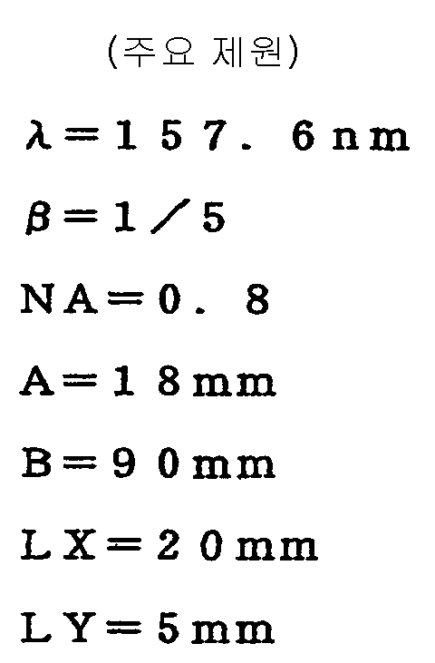
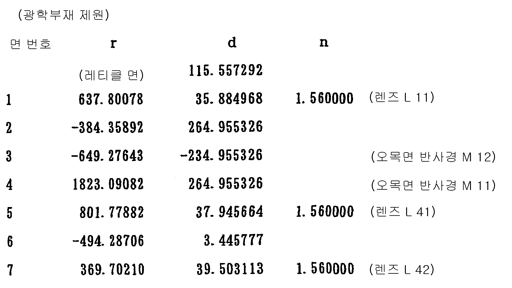

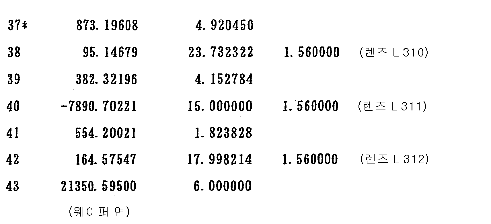
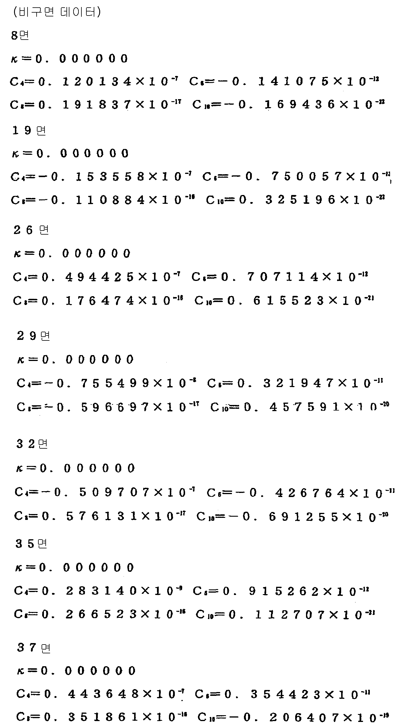
도 9는 제 3 실시예에 관한 반사굴절광학계의 가로수차를 도시한 도면이다. 수차도에서 Y는 상 높이(㎜)를 도시하고 있다. 수차도로부터 밝혀진 바와 같이 제 3 실시예에서는 파장폭이 157.6㎚±0.3pm의 노광광에 대해서 색수차가 양호하게 보정되어 있는 것을 알 수 있다. 또한, 구면수차, 코머수차, 비점수차, 디스토션(왜곡수차)이 거의 무수차에 가까운 상태까지 양호하게 보정되고, 우수한 결상성능을 갖는 것을 확인하고 있다.9 is a diagram showing the horizontal aberration of the reflection refractive optical system according to the third embodiment. Y in the aberration diagram shows the image height in mm. As is clear from the aberration diagram, it can be seen that in the third embodiment, chromatic aberration is well corrected for exposure light having a wavelength width of 157.6 nm ± 0.3 pm. In addition, it has been confirmed that spherical aberration, comer aberration, astigmatism, and distortion (distortion aberration) are well corrected to almost an aberration, and have excellent imaging performance.
(제 4 실시예)(Example 4)
도 10은 제 4 실시예에 관한 반사굴절광학계(촬영광학계(PL))의 렌즈 구성을 도시한 도면이다. 도 10의 반사굴절광학계에서 제 1 결상광학계(G1)는 레티클측부터 차례로, 웨이퍼측에 비구면 형상의 볼록면을 향한 양볼록렌즈(L11)와, 웨이퍼측에 비구면 형상의 오목면을 향한 부 메니스커스렌즈(L12)와, 웨이퍼측에 평면에 가까운 오목면을 향한 오목면 반사경(M11)과, 레티클측에 오목면을 향한 부 메니스커스렌즈(L13)와, 레티클측에 오목면을 향한 오목면 반사경(M12)으로 구성되어 있다.FIG. 10 is a diagram showing a lens configuration of a reflection refractive optical system (imaging optical system PL) according to the fourth embodiment. In the reflective refraction optical system of FIG. 10, the first imaging optical system G1 has a biconvex lens L11 toward the aspherical convex surface on the wafer side and a convex concave surface on the wafer side from the reticle side. The varnish lens L12, the concave reflecting mirror M11 facing the plane near the plane on the wafer side, the sub meniscus lens L13 facing the concave surface on the reticle side, and the concave surface toward the reticle side. It is comprised by the concave reflecting mirror M12.
또한, 제 2 결상광학계(G2)는 레티클측부터 차례로, 웨이퍼측에 오목면을 향한 오목면 반사경(M21)과, 레티클측에 볼록면을 향한 부 메니스커스렌즈(L21)와, 레티클측에 평면에 가까운 오목면을 향한 오목면 반사경(M22)으로 구성되어 있다.The second imaging optical system G2 has a concave reflecting mirror M21 facing the concave surface on the wafer side, a sub meniscus lens L21 facing the convex surface on the reticle side, and a reticle side from the reticle side. It is comprised by the concave reflecting mirror M22 toward the concave surface near a plane.
또한, 제 3 결상광학계(G3)는 레티클측부터 차례로, 웨이퍼측에 비구면형상의 오목면을 향한 정 메니스커스렌즈(L31)와, 웨이퍼측에 비구면 형상의 오목면을 향한 부 메니스커스렌즈(L32)와, 웨이퍼측에 비구면 형상의 오목면을 향한 정 메니스커스렌즈(L33)와, 개구 조리개(AS)와, 레티클측에 비구면 형상의 오목면을 향한 정 메니스커스렌즈(L34)와, 레티클측에 볼록면을 향한 정 메니스커스렌즈(L35)와, 웨이퍼측에 비구면 형상의 오목면을 향한 정 메니스커스렌즈(L36)와, 웨이퍼측에 비구면형상의 볼록면을 향한 양볼록렌즈(L37)와, 웨이퍼측에 비구면형상의 오목면을 향한 정 메니스커스렌즈(L38)와, 레티클측에 비구면 형상의 볼록면을 향한 정 메니스커스렌즈(L39)로 구성되어 있다.In addition, the third imaging optical system G3 has a positive meniscus lens L31 facing the aspherical concave surface on the wafer side and a minor meniscus lens facing the aspherical concave surface on the wafer side from the reticle side. (L32), positive meniscus lens L33 facing the aspherical concave surface on the wafer side, aperture diaphragm AS, and positive meniscus lens L34 facing the aspherical concave surface on the reticle side And a positive meniscus lens L35 facing the convex surface on the reticle side, a positive meniscus lens L36 facing the concave surface on the wafer side and an aspherical convex surface on the wafer side. It consists of the convex lens L37, the positive meniscus lens L38 which faces the aspherical concave surface on the wafer side, and the positive meniscus lens L39 which faces the aspherical convex surface on the reticle side.
또한, 제 1 결상광학계(G1)와 제 2 결상광학계(G2) 사이의 광로중에는 레티클측부터 차례로, 레티클측에 볼록면을 향한 정 메니스커스렌즈(L41)와, 웨이퍼측에 비구면형상의 오목면을 향한 정 메니스커스렌즈(L42)와, 웨이퍼측에 비구면형상의 오목면을 향한 정 메니스커스렌즈(L43)으로 구성된 제 1 필드렌즈가 배치되어 있다. 또한, 제 2 결상광학계(G2)와 제 3 결상광학계(G3) 사이의 광로중에는 레티클측부터 차례로, 웨이퍼측에 비구면 형상의 오목면을 향한 정 메니스커스렌즈(L51)와, 웨이퍼측에 비구면 형상의 볼록면을 향한 양볼록렌즈(L52)로 구성된 제 2 필드렌즈가 배치되어 있다.In addition, in the optical path between the first imaging optical system G1 and the second imaging optical system G2, the positive meniscus lens L41 faces the convex surface on the reticle side in order from the reticle side, and the aspherical recess on the wafer side. The first field lens composed of the positive meniscus lens L42 facing the surface and the positive meniscus lens L43 facing the aspherical concave surface is disposed on the wafer side. In addition, in the optical path between the second imaging optical system G2 and the third imaging optical system G3, the positive meniscus lens L51 faces the aspherical concave surface on the wafer side from the reticle side, and aspherical surface on the wafer side. The second field lens composed of the biconvex lens L52 facing the convex surface of the shape is arranged.
따라서, 제 4 실시예에서는 레티클(R)로부터의 광이 양볼록렌즈(L11), 부 메니스커스렌즈(L12) 및 부 메니스커스렌즈(L13)를 통하여, 오목면 반사경(M12)에 입사한다. 오목면 반사경(M12)에서 반사된 광은 부 메니스커스렌즈(L13)를 통하여 오목면 반사경(M11)에서 반사된 후, 제 1 필드렌즈(L41~L43) 중에 레티클 패턴의 제 1 중간상을 형성한다.Therefore, in the fourth embodiment, light from the reticle R is incident on the concave reflecting mirror M12 through the biconvex lens L11, the sub meniscus lens L12 and the sub meniscus lens L13. do. The light reflected by the concave reflector M12 is reflected by the concave reflector M11 through the sub meniscus lens L13, and then forms a first intermediate image of the reticle pattern in the first field lenses L41 to L43. do.
제 1 필드렌즈(L41~L43) 중에 형성된 제 1 중간상으로부터의 광은, 오목면 반사경(M22)에서 반사되고 부 메니스커스렌즈(L21)를 통하여 오목면 반사경(M21)에서 반사된 후, 부 메니스커스렌즈(L21)를 통하여 제 2 필드렌즈(L51 및 L52) 중에 레티클 패턴의 제 2 중간상을 형성한다. 제 2 필드렌즈(L51 및 L52) 중에 형성된 제 2 중간상으로부터의 광은 제 3 결상광학계(G3)를 구성하는 각 렌즈(L31~L39)를 통하여, 웨이퍼(W)상에 레티클 패턴의 최종상을 형성한다.The light from the first intermediate image formed in the first field lenses L41 to L43 is reflected by the concave reflector M22 and reflected by the concave reflector M21 through the sub meniscus lens L21, and then is negative. A second intermediate image of the reticle pattern is formed in the second field lenses L51 and L52 through the meniscus lens L21. Light from the second intermediate image formed in the second field lenses L51 and L52 forms the final image of the reticle pattern on the wafer W through the respective lenses L31 to L39 constituting the third imaging optical system G3. do.
다음의 표 4에, 제 4 실시예의 반사굴절광학계의 제원의 값을 든다. 표 4의 주요제원에서, λ는 노광광의 중심파장을, β는 투영배율(전체계의 결상배율)을, NA는 상측(웨이퍼측) 개구수를, A는 웨이퍼(W)상에서의 이미지 서클(IF)의 반경 즉 최대 상 높이를, B는 최대 상 높이(A)에 대응하는 최대 물체 높이를, LX는 실효노광영역(ER)의 X방향을 따른 크기(장변의 크기)를, LY는 실효노광영역(ER)의 Y방향을 따른 크기(단변의 크기)를 각각 나타내고 있다.In Table 4 below, the values of the specifications of the reflective refractive optical system of the fourth embodiment are given. In the main specifications of Table 4, λ is the center wavelength of the exposure light, β is the projection magnification (imaging of the whole system), NA is the numerical aperture on the upper side (wafer side), and A is the image circle on the wafer W ( IF), that is, the maximum image height, B is the maximum object height corresponding to the maximum image height A, LX is the size (length of the long side) along the X direction of the effective exposure area ER, and LY is the effective value. The magnitude | size (short side size) in the Y direction of the exposure area ER is shown, respectively.
또한, 표 4의 광학부재 제원에서 제 1 컬럼의 면번호는 레티클측으로부터의 면의 순서를, 제 2 컬럼의 r은 각 면의 곡률반경(비구면의 경우에는 정점곡률반경:㎜)을, 제 3 컬럼의 d는 각 면의 축상간격 즉 면간격(㎜)을, 제 4 컬럼의 n은 중심파장에 대한 굴절율을 각각 나타내고 있다. 또한, 면간격(d)은 반사될 때마다 그 부호를 변화시키는 것으로 한다. 따라서, 면간격(d)의 부호는 오목면 반사경(M12)으로부터 오목면 반사경(M11)으로의 광로 중 및 오목면 반사경(M22)으로부터 오목면 반사경(M21)으로의 광로 중에서는 부로 하고, 그 밖의 광로 중에서는 정으로 하고 있다. 또한, 광의 입사방향에 관계없이, 레티클측을 향하여 볼록면의 곡률반경을 정으로 하고, 레티클측을 향하여 오목면의 곡률반경을 부로 하고 있다. In addition, in the optical member specifications of Table 4, the surface number of the first column is the order of the surface from the reticle side, and the r of the second column is the radius of curvature of each surface (vertical radius of curvature: mm) in the case of aspherical surface. D in each of the three columns represents the axial spacing of each surface, that is, the surface spacing (mm), and n in the fourth column represents the refractive index with respect to the center wavelength. It is to be noted that the plane interval d changes its sign every time it is reflected. Therefore, the sign of the surface interval d is negative in the optical path from the concave reflector M12 to the concave reflector M11 and in the optical path from the concave reflector M22 to the concave reflector M21, In the outside light path, it is set as positive. Regardless of the direction of incidence of light, the radius of curvature of the convex surface is set toward the reticle side, and the radius of curvature of the concave surface is made negative toward the reticle side.
(표 4)Table 4
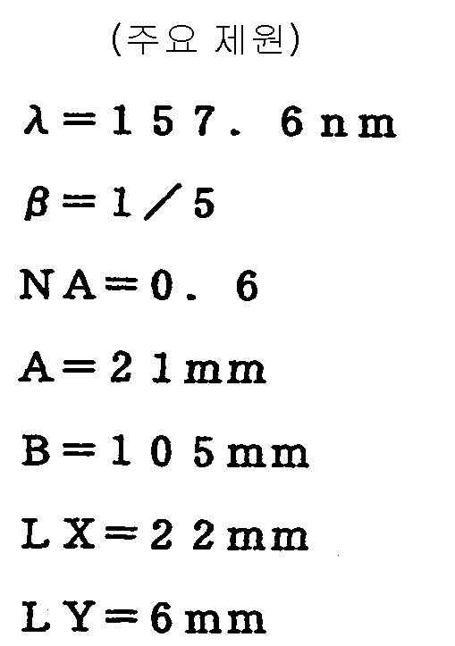
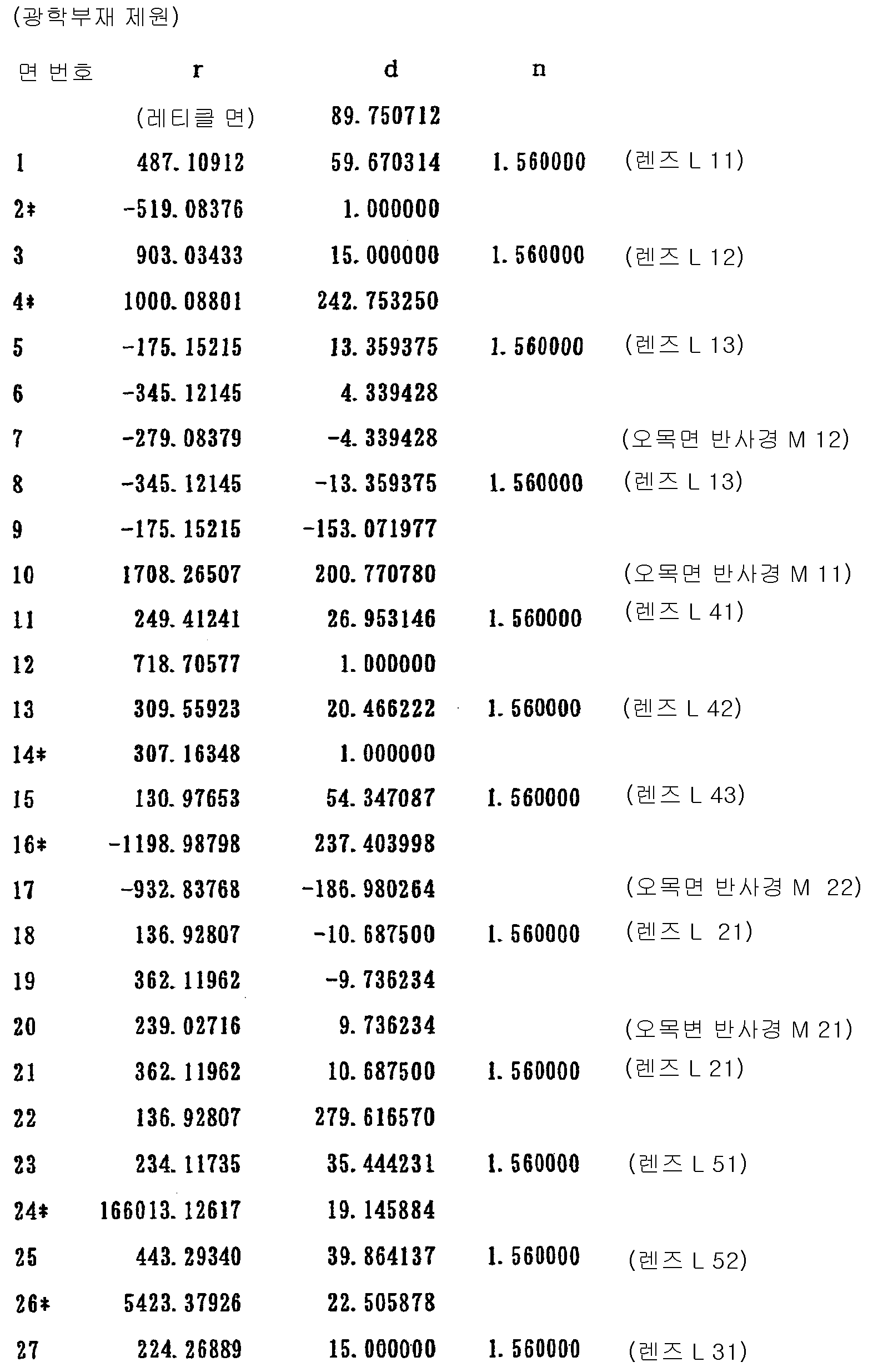
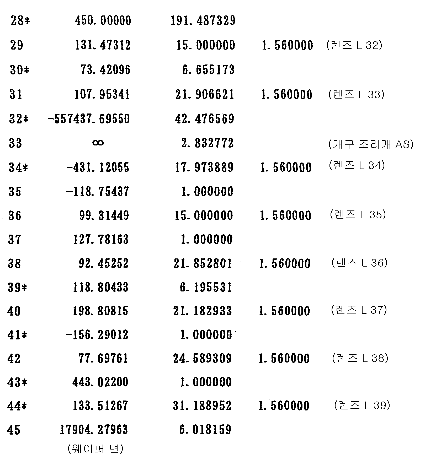
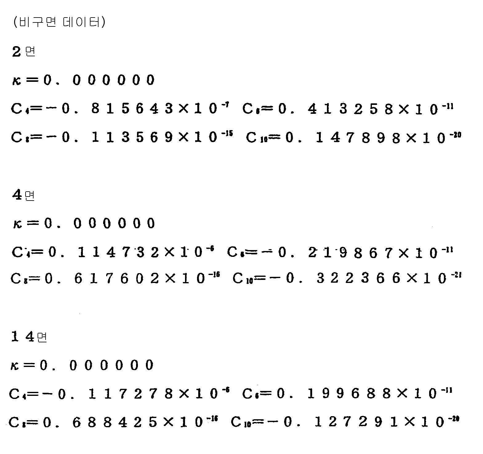

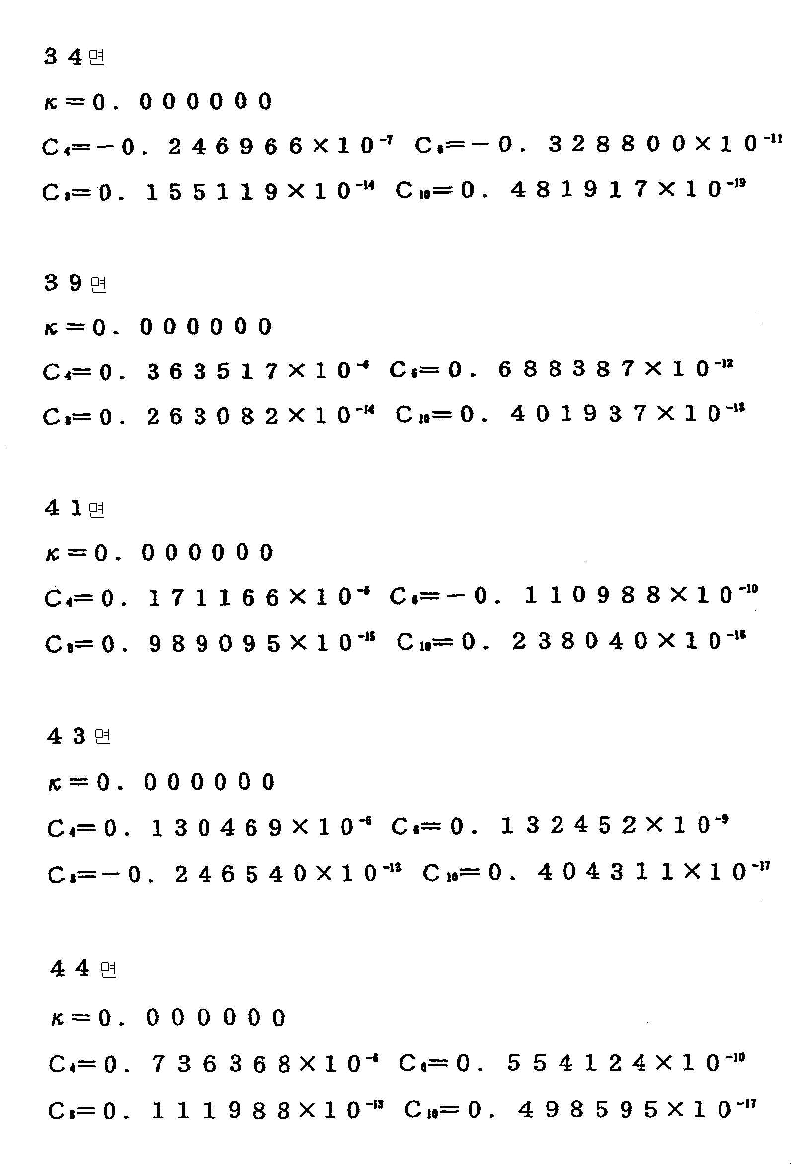
도 11은 제 4 실시예에 관한 반사굴절광학계의 가로수차를 도시한 도면이다. 수차도에서 Y는 상 높이(㎜)를 나타내고 있다. 수차도로부터 밝혀진 바와 같이, 제 4 실시예에서도 제 1 실시예 및 제 2 실시예와 동일하게, 파장폭이 157.6㎚±0.5pm의 노광광에 대해서 색수차가 양호하게 보정되어 있는 것을 알 수 있다. 또한, 구면수차, 코머수차, 비점수차, 디스토션(왜곡수차)이 거의 무수차에 가까운 상태까지 양호하게 보정되고, 우수한 결상성능을 갖는 것을 확인하고 있다.Fig. 11 is a diagram showing the horizontal aberration of the reflective refractive optical system according to the fourth embodiment. In the aberration diagram, Y represents the image height (mm). As is clear from the aberration diagram, it can be seen that the chromatic aberration is well corrected for the exposure light having a wavelength width of 157.6 nm ± 0.5 pm, similarly to the first and second embodiments in the fourth embodiment. In addition, it has been confirmed that spherical aberration, comer aberration, astigmatism, and distortion (distortion aberration) are well corrected to almost an aberration, and have excellent imaging performance.
(제 5 실시예)(Example 5)
도 12는 제 5 실시예에 관한 반사굴절광학계(투영광학계(PL))의 렌즈 구성을 도시한 도면이다. 도 12의 반사굴절광학계에서 제 1 결상광학계(G1)는 레티클측부터 차례로, 레티클측에 볼록면을 향한 정 메니스커스렌즈(L11)와, 웨이퍼측에 평면에 가까운 오목면을 향한 오목면 반사경(M11)과, 레티클측에 오목면을 향한 부 메니스커스렌즈(L12)와, 레티클측에 오목면을 향한 오목면 반사경(M12)으로 구성되어 있다.FIG. 12 is a diagram showing a lens configuration of a reflective refractive optical system (projection optical system PL) according to the fifth embodiment. In the reflective refractive optical system of Fig. 12, the first imaging optical system G1 has a positive meniscus lens L11 facing the convex surface on the reticle side, and a concave reflecting mirror facing the plane near the plane on the reticle side. (M11), the sub meniscus lens L12 facing the concave surface on the reticle side, and the concave reflecting mirror M12 facing the concave surface on the reticle side.
또한, 제 2 결상광학계(G2)는 레티클측부터 차례로, 웨이퍼측에 오목면을 향한 오목면 반사경(M21)과, 레티클측에 평면에 가까운 오목면을 향한 오목면 반사경(M22)으로 구성되어 있다.The second imaging optical system G2 is composed of a concave reflecting mirror M21 facing the concave surface on the wafer side and a concave reflecting mirror M22 facing the concave surface close to the plane on the reticle side. .
또한, 제 3 결상광학계(G3)는 레티클측부터 차례로, 양오목렌즈(L31)와, 웨이퍼측에 비구면 형상의 오목면을 향한 정 메니스커스렌즈(L32)와, 양볼록렌즈(L33)와, 레티클측에 볼록면을 향한 부 메니스커스렌즈(L34)와, 레티클측에 볼록면을 향한 정 메니스커스렌즈(L35)와, 웨이퍼측에 비구면 형상의 오목면을 향한 정 메니스커스렌즈(L36)와, 양볼록렌즈(L37)와, 레티클측에 오목면을 향한 부 메니스커스렌즈(L38)와, 개구 조리개(AS)와, 레티클측에 비구면 형상의 오목면을 향한 부 메니스커스렌즈(L39)와, 웨이퍼측에 비구면 형상의 볼록면을 향한 양볼 록렌즈(L310)와, 레티클측에 오목면을 향한 부 메니스커스렌즈(L311)와, 웨이퍼측에 비구면 형상의 오목면을 향한 정 메니스커스렌즈(L312)와, 레티클측에 볼록면을 향한 정 메니스커스렌즈(L313)와, 레티클측에 볼록면을 향한 정 메니스커스렌즈(L314)와, 양볼록렌즈(L315)로 구성되어 있다.In addition, the third imaging optical system G3 has a biconvex lens L31, a positive meniscus lens L32 facing an aspherical concave surface on the wafer side, and a biconvex lens L33 in order from the reticle side. The secondary meniscus lens L34 facing the convex surface on the reticle side, the positive meniscus lens L35 facing the convex surface on the reticle side, and the positive meniscus lens facing the concave surface of the aspherical surface on the wafer side. (L36), the biconvex lens L37, the sub meniscus lens L38 facing the concave surface on the reticle side, the aperture stop AS, and the sub menisc facing the concave surface of the aspherical shape on the reticle side. The curse lens L39, the biconvex lens L310 facing the aspherical convex surface on the wafer side, the sub meniscus lens L311 facing the concave surface on the reticle side, and the aspherical concave surface on the wafer side The positive meniscus lens L312 facing toward the lens, the positive meniscus lens L313 facing toward the reticle side, and the convex surface facing the reticle side. Facing positive meniscus lens L314 and biconvex lens L315.
또한, 제 1 결상광학계(G1)와 제 2 결상광학계(G2) 사이의 광로중에는 레티클측부터 차례로, 양볼록렌즈(L41)와, 웨이퍼측에 비구면 형상의 오목면을 향한 정 메니스커스렌즈(L42)로 구성된 제 1 필드렌즈가 배치되어 있다. 또한, 제 2 결상광학계(G2)와 제 3 결상광학계(G3) 사이의 광로중에는 레티클측부터 차례로, 레티클측에 비구면 형상의 오목면을 향한 정 메니스커스렌즈(L51)와, 양볼록렌즈(L52)로 구성된 제 2 필드렌즈가 배치되어 있다.In addition, in the optical path between the first imaging optical system G1 and the second imaging optical system G2, the biconvex lens L41 and the positive meniscus lens facing the concave surface of the aspherical surface on the wafer side in turn from the reticle side ( A first field lens composed of L42) is disposed. In addition, in the optical path between the second imaging optical system G2 and the third imaging optical system G3, the positive meniscus lens L51 and the biconvex lens (in order from the reticle side toward the aspherical concave surface on the reticle side). A second field lens composed of L52 is disposed.
따라서, 제 5 실시예에서는 레티클(R)로부터의 광이 정 메니스커스렌즈(L11) 및 부 메니스커스렌즈(L12)를 통하여 오목면 반사경(M12)에 입사한다. 오목면 반사경(M12)에서 반사된 광은 부 메니스커스렌즈(L12)를 통하여 오목면 반사경(M11)에서 반사된 후, 제 1 필드렌즈(L41 및 L42)의 근방에 레티클 패턴의 제 1 중간상을 형성한다.Therefore, in the fifth embodiment, light from the reticle R is incident on the concave reflecting mirror M12 through the positive meniscus lens L11 and the secondary meniscus lens L12. The light reflected by the concave reflector M12 is reflected by the concave reflector M11 through the sub meniscus lens L12, and then the first intermediate image of the reticle pattern near the first field lenses L41 and L42. To form.
제 1 중간상으로부터의 광은 제 1 필드렌즈(L41 및 L42)를 통하여 오목면 반사경(M22) 및 오목면 반사경(M21)에서 차례로 반사된 후, 제 2 필드렌즈(L51 및 L52)의 근방에 레티클 패턴의 제 2 중간상을 형성한다. 제 2 중간상으로부터의 광은 제 2 필드렌즈(L51 및 L52), 및 제 3 결상광학계(G3)를 구성하는 각 렌즈(L31~L315)를 통하여 웨이퍼(W)상에 레티클 패턴의 최종상을 형성한다. Light from the first intermediate image is sequentially reflected by the concave reflector M22 and the concave reflector M21 through the first field lenses L41 and L42, and then reticle near the second field lenses L51 and L52. The second intermediate phase of the pattern is formed. Light from the second intermediate image forms a final image of the reticle pattern on the wafer W through the second field lenses L51 and L52 and the respective lenses L31 to L315 constituting the third imaging optical system G3. .
다음의 표 5에, 제 5 실시예의 반사굴절광학계의 제원의 값을 든다. 표 5의 주요제원에서, λ는 노광광의 중심파장을, β는 투영배율(전체계의 결상배율)을, NA는 상측(웨이퍼측) 개구수를, A는 웨이퍼(W)상에서의 이미지 서클(IF)의 반경 즉 최대 상 높이를, B는 최대 상 높이(A)에 대응하는 최대 물체 높이를, LX는 실효노광영역(ER)의 X방향을 따른 크기(장변의 크기)를, LY는 실효노광영역(ER)의 Y방향을 따른 크기(단변의 크기)를 각각 나타내고 있다.Table 5 below shows the values of the specifications of the reflective refractive optical system of the fifth embodiment. In the main specifications of Table 5, λ is the center wavelength of the exposure light, β is the projection magnification (imaging of the whole system), NA is the numerical aperture on the image side (wafer side), and A is the image circle on the wafer W ( IF), that is, the maximum image height, B is the maximum object height corresponding to the maximum image height A, LX is the size (length of the long side) along the X direction of the effective exposure area ER, and LY is the effective value. The magnitude | size (short side size) in the Y direction of the exposure area ER is shown, respectively.
또한, 표 5의 광학부재 제원에서 제 1 컬럼의 면 번호는 레티클측으로부터의 면의 순서를, 제 2 컬럼의 r은 각 면의 곡률반경(비구면의 경우에는 정점곡률반경:㎜)을, 제 3 컬럼의 d는 각 면의 축상간격 즉 면간격(㎜)을, 제 4 컬럼의 n은 중심파장에 대한 굴절율을 각각 나타내고 있다. 또한, 면간격(d)은 반사될 때마다 그 부호를 바꾸는 것으로 한다. 따라서, 면간격(d)의 부호는 오목면 반사경(M12)으로부터 오목면 반사경(M11)으로의 광로 중 및 오목면 반사경(M22)으로부터 오목면 반사경(M21)으로의 광로 중에서는 부로 하고, 그 외의 광로 중에서는 정으로 하고 있다. 또, 광의 입사방향에 상관없이, 레티클측을 향해 볼록면의 곡률반경을 정으로 하고, 레티클측으로 향해 오목면의 곡률반경을 부로 하고 있다. In addition, in the optical member specifications of Table 5, the surface number of the first column is the order of the surfaces from the reticle side, and the r of the second column is the radius of curvature of each surface (vertical radius of curvature: mm). D in each of the three columns represents the axial spacing of each surface, that is, the surface spacing (mm), and n in the fourth column represents the refractive index with respect to the center wavelength. It is to be noted that the plane interval d changes its sign every time it is reflected. Therefore, the sign of the surface interval d is negative in the optical path from the concave reflector M12 to the concave reflector M11 and in the optical path from the concave reflector M22 to the concave reflector M21, In other light paths, it is set as positive. Regardless of the incident direction of light, the radius of curvature of the convex surface is set toward the reticle side, and the radius of curvature of the concave surface is made negative toward the reticle side.
(표 5)Table 5
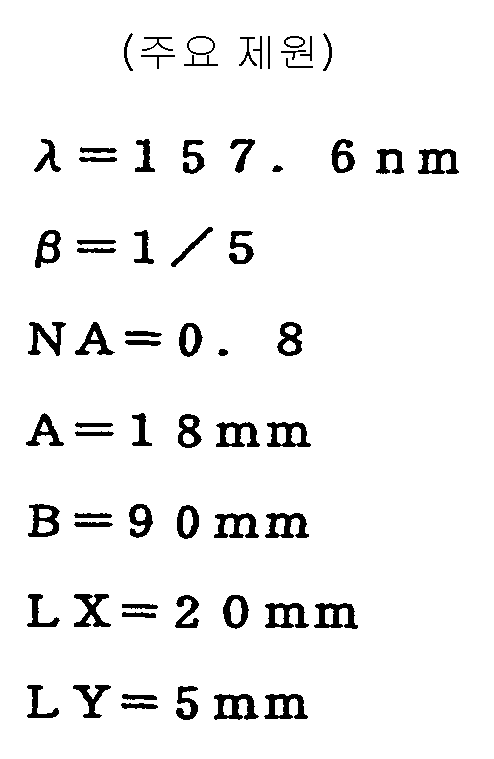

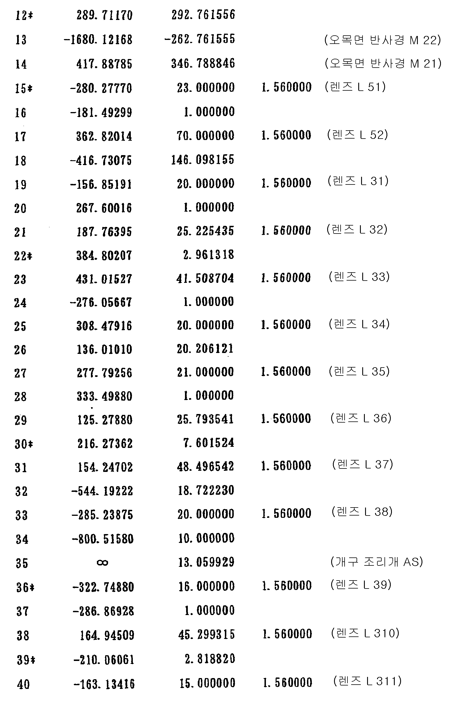


도 13은 제 5 실시예에 따른 반사굴절광학계의 가로수차를 나타내는 도면이다. 수차도에 있어서, Y는 상 높이(mm)를 나타내고 있다. 수차도로부터 명확해진 바와 같이 제 5 실시예에서도 제 3 실시예와 마찬가지로, 파장폭이 157.6nm±0.3pm의 노광광에 대해 색수차가 양호하게 보정되어 있는 것을 알 수 있다. 또, 구면수차, 코머수차, 비점수차, 디스토션(왜곡수차)이 거의 무수차에 가까운 상태까지 양호하게 보정되고, 우수한 결상성능을 갖는 것이 확인되고 있다.FIG. 13 is a diagram showing lateral aberration of the reflective refractive optical system according to the fifth embodiment. FIG. In the aberration diagram, Y represents the image height (mm). As is clear from the aberration diagram, in the fifth embodiment as well as the third embodiment, it can be seen that chromatic aberration is well corrected for the exposure light having a wavelength width of 157.6 nm ± 0.3 pm. In addition, it has been confirmed that spherical aberration, comer aberration, astigmatism, and distortion (distortion aberration) are well corrected to a state almost close to aberration, and have excellent imaging performance.
(제 6 실시예)(Example 6)
도 14는 제 6 실시예에 따른 반사굴절광학계(투영광학계(PL))의 렌즈 구성을 나타내는 도면이다. 도 14의 반사굴절광학계에 있어서, 제 1 결상광학계(G1)는 레티클측으로부터 차례로, 레티클측에 볼록면을 향하게 한 정 메니스커스렌즈(L11)와, 웨이퍼측에 평면에 가까운 오목면을 향하게 한 오목면 반사경(M11)과, 레티클측에 오목면을 향하게 한 오목면 반사경(M12)으로 구성되어 있다.FIG. 14 is a view showing the lens configuration of the reflective refractive optical system (projection optical system PL) according to the sixth embodiment. In the reflective refractive optical system of Fig. 14, the first imaging optical system G1 is in turn from the reticle side to the positive meniscus lens L11 with the convex surface facing the reticle side and the concave surface close to the plane on the wafer side. It consists of one concave reflecting mirror M11 and the concave reflecting mirror M12 which made the concave surface facing the reticle side.
또, 제 2 결상광학계(G2)는 레티클측으로부터 차례로, 웨이퍼측에 오목면을 향하게 한 오목면 반사경(M21)과, 레티클측에 볼록면을 향하게 한 부 메니스커스렌즈(L21)와, 레티클측에 평면에 가까운 오목면을 향하게 한 오목면 반사경(M22)으로 구성되어 있다.The second imaging optical system G2 has a concave reflecting mirror M21 with the concave surface facing the wafer side in turn from the reticle side, a sub meniscus lens L21 with the convex surface facing the reticle side, and a reticle. It is comprised by the concave reflecting mirror M22 which faced the concave surface near a plane at the side.
또, 제 3 결상광학계(G3)는 레티클측에서 차례로, 양오목렌즈(L31)와, 웨이퍼측에 비구면형상의 오목면을 향하게 한 부 메니스커스렌즈(L32)와, 레티클측에 볼록면을 향하게 한 정 메니스커스렌즈(L33)와, 양오목렌즈(L34)와, 레티클측에 오목면을 향하게 한 부 메니스커스렌즈(L35)와, 웨이퍼측에 비구면형상의 오목면을 향하게 한 정 메니스커스렌즈(L36)와, 양볼록렌즈(L37)와, 레티클측으로 오목면을 향하게 한 부 메니스커스렌즈(L38)와, 개구 조리개(AS)와, 레티클측으로 비구면형 상의 오목면을 향하게 한 정 메니스커스렌즈(L39)와, 웨이퍼측에 비구면형상의 볼록면을 향하게 한 양볼록렌즈(L310)와, 레티클측으로 오목면을 향하게 한 부 메니스커스렌즈(L311)와, 웨이퍼측으로 비구면형상의 오목면을 향하게 한 정 메니스커스렌즈(L312)와, 레티클측으로 볼록면을 향하게 한 정 메니스커스렌즈(L313)와, 레티클측으로 볼록면을 향하게 한 부 메니스커스렌즈(L314)와, 양볼록렌즈(L315)로 구성되어 있다.The third imaging optical system G3 sequentially has a biconvex lens L31 on the reticle side, a secondary meniscus lens L32 facing the aspherical concave surface on the wafer side, and a convex surface on the reticle side. Oriented tablets Meniscus lens (L33), biconvex lens (L34), secondary meniscus lens (L35) facing the concave surface on the reticle side, and tablets facing the concave surface on the wafer side The meniscus lens L36, the biconvex lens L37, the sub meniscus lens L38 facing the concave surface toward the reticle side, the aperture diaphragm AS, and the concave surface facing the aspheric shape toward the reticle side. The fixed meniscus lens L39, the biconvex lens L310 facing the convex surface of the aspherical surface on the wafer side, the sub meniscus lens L311 facing the concave surface toward the reticle side, and the aspherical surface toward the wafer side The positive meniscus lens L312 facing the concave surface of the shape and the convex surface toward the reticle side May be one composed of positive meniscus lenses (L313), and a convex and a surface facing the negative meniscus lens (L314), biconvex lens (L315) the reticle side.
또, 제 1 결상광학계(G1)와 제 2 결상광학계(G2)의 사이의 광로 중에는 레티클측에서 차례로, 레티클측으로 오목면을 향하게 한 정 메니스커스렌즈(L41)와, 웨이퍼측으로 비구면형상의 볼록면을 향하게 한 양볼록렌즈(L42)로 구성된 제 1 필드렌즈가 배치되어 있다. 또, 제 2 결상광학계(G2)와 제 3 결상광학계(G3)의 사이의 광로 중에는 레티클측에서 차례로, 레티클측으로 비구면형상의 볼록면을 향하게 한 양볼록렌즈(L51)와, 양볼록렌즈(L52)로 구성된 제 2 필드렌즈가 배치되어 있다.In addition, in the optical path between the first imaging optical system G1 and the second imaging optical system G2, the positive meniscus lens L41 with the concave surface facing the reticle side in turn from the reticle side, and the aspherical convex toward the wafer side. The first field lens composed of the biconvex lens L42 facing the surface is arranged. In addition, in the optical path between the second imaging optical system G2 and the third imaging optical system G3, the biconvex lens L51 and the biconvex lens L52 which in turn face the convex surface aspherical toward the reticle side from the reticle side The second field lens composed of) is arranged.
따라서, 제 6 실시예에서는 레티클(R)로부터의 광이 정 메니스커스렌즈(L11)를 통해 오목면 반사경(M12)으로 입사한다. 오목면 반사경(M12)에서 반사된 광은 오목면 반사경(M11)에서 반사된 후, 제 1 필드 렌즈(L41 및 L42) 중에 레티클 패턴의 제 1 중간상을 형성한다.Therefore, in the sixth embodiment, light from the reticle R is incident on the concave reflecting mirror M12 through the positive meniscus lens L11. The light reflected by the concave reflector M12 is reflected by the concave reflector M11, and then forms the first intermediate image of the reticle pattern in the first field lenses L41 and L42.
제 1 필드렌즈(L41 및 L42) 중에 형성된 제 1 중간상으로부터의 광은 오목면 반사경(M22)에서 반사되고, 부 메니스커스렌즈(L21)를 통해 오목면 반사경(M21)에서 반사된 후, 부 메니스커스렌즈(L21)를 통해 제 2 필드렌즈(L51 및 L52)의 근방에 레티클 패턴의 제 2 중간상을 형성한다. 제 2 중간상으로부터의 광은 제 2 필 드 렌즈(L51 및 L52) 및 제 3 결상광학계(G3)를 구성하는 각 렌즈(L31∼L315)를 통해 웨이퍼(W)상에 레티클 패턴의 최종 상을 형성한다.Light from the first intermediate image formed in the first field lenses L41 and L42 is reflected by the concave reflector M22, and is reflected by the concave reflector M21 through the sub meniscus lens L21, and then A second intermediate image of the reticle pattern is formed in the vicinity of the second field lenses L51 and L52 through the meniscus lens L21. Light from the second intermediate image forms a final image of the reticle pattern on the wafer W through the respective lenses L31 to L315 constituting the second field lenses L51 and L52 and the third imaging optical system G3. do.
또, 상술한 제 1 실시예∼제 5 실시예에서는 웨이퍼(W)상에 직사각형 형상의 실효노광영역(ER)이 형성되지만, 제 6 실시예에서는 원호형상의 실효노광영역(ER)이 형성된다. 도 15는 제 6 실시예에서 웨이퍼 상에 형성되는 원호형상의 실효노광영역과 기준 광축의 위치관계를 나타내는 도면이다. 도 15에 도시한 바와 같이, 제 6 실시예에서는 기준 광축(AX)을 중심으로 하여 반경(A)(최대 상 높이에 대응)을 갖는 원 형상의 영역(이미지 서클)(IF)내에서 기준 광축(AX)으로부터 +Y방향으로 편심한 위치에 원하는 크기를 갖는 원호형상의 실효노광영역(ER)이 설정되어 있다. 여기서, 원호형상의 실효노광영역(ER)의 X방향의 길이는 LX’이며, 그 Y방향의 길이는 LY’이다. 따라서, 레티클(R)상에서는 기준 광축(AX)으로부터 -Y방향으로 편심한 위치에 원호형상의 실효노광영역(ER)에 대응한 크기 및 형상을 갖는 원호형상의 조명영역(IR)이 형성되어 있게 된다. 즉, 기준 광축(AX)을 중심으로 한 반경(B)(최대 물체 높이에 대응)을 갖는 원 형상의 영역내에 있어서, 기준 광축(AX)으로부터 -Y방향으로 편심한 위치에 원하는 크기를 갖는 원호형상의 조명영역(IR)이 설정되어 있다.Incidentally, in the first to fifth embodiments described above, the rectangular effective exposure area ER is formed on the wafer W. In the sixth embodiment, an arc-shaped effective exposure area ER is formed. . FIG. 15 is a diagram showing the positional relationship between the arc-shaped effective exposure area formed on the wafer and the reference optical axis in the sixth embodiment. As shown in Fig. 15, in the sixth embodiment, the reference optical axis is located within a circular area (image circle) IF having a radius A (corresponding to the maximum image height) centered on the reference optical axis AX. An arc-shaped effective exposure area ER having a desired size is set at a position eccentric to + Y from (AX). Here, the length in the X direction of the arc-shaped effective exposure area ER is LX ', and the length in the Y direction is LY'. Therefore, on the reticle R, an arc-shaped illumination region IR having a size and shape corresponding to the arc-shaped effective exposure region ER is formed at a position eccentric to the -Y direction from the reference optical axis AX. do. That is, a circular arc having a desired size at a position eccentric in the -Y direction from the reference optical axis AX in a circular region having a radius B (corresponding to the maximum object height) around the reference optical axis AX. The illumination region IR of the shape is set.
다음의 표 6에, 제 6 실시예의 반사굴절광학계의 제원의 값을 든다. 표 6의 주요 제원에 있어서, λ은 노광광의 중심 파장을, β는 투영배율(전체계의 결상배율)을, NA는 상측(웨이퍼측) 개구수를, A는 웨이퍼(W)상에서의 이미지 서클(IF)의 반경, 즉 최대 상 높이를, B는 최대 상 높이(A)에 대응하는 최대 물체 높이를, LX ’는 원호형상의 실효노광영역(ER)의 X방향을 따르는 치수를, LY’는 원호형상의 실효노광영역(ER)의 Y방향을 따르는 치수를 각각 나타내고 있다.Table 6 below shows the values of the specifications of the reflective refractive optical system of the sixth embodiment. In the main specifications of Table 6, λ is the center wavelength of the exposure light, β is the projection magnification (image-forming magnification of the entire system), NA is the numerical aperture on the image side (wafer side), and A is the image circle on the wafer W. The radius of (IF), i.e. the maximum image height, B is the maximum object height corresponding to the maximum image height A, LX 'is the dimension along the X direction of the arc-shaped effective exposure area ER, LY' Denotes dimensions along the Y direction of the arc-shaped effective exposure region ER, respectively.
또, 표 6의 광학부재 제원에 있어서, 제 1 컬럼의 면 번호는 레티클측으로부터의 면의 순서를, 제 2 컬럼의 r은 각 면의 곡률반경(비구면의 경우에는 정점 곡률반경:mm)을, 제 3 컬럼의 d는 각 면의 축상간격, 즉 면간격(mm)을, 제 4 컬럼의 n은 중심파장에 대한 굴절율을 각각 나타내고 있다. 또, 면간격(d)은 반사될 때 마다 그 부호를 바꾸는 것으로 한다. 따라서, 면간격(d)의 부호는 오목면 반사경(M12)으로부터 오목면 반사경(M11)으로의 광로 중 및 오목면 반사경(M22)으로부터 오목면 반사경(M21)으로의 광로 중에서는 부로 하고, 그 외의 광로 중에서는 정으로 하고 있다. 또, 광의 입사방향에 상관없이 레티클측을 향해 볼록면의 곡률반경을 정으로 하고, 레티클측을 향해 오목면의 곡률반경을 부로 하고 있다.In the optical member specifications of Table 6, the surface number of the first column is the order of the surface from the reticle side, and the r of the second column is the radius of curvature of each surface (vertical radius of curvature: mm). , D in the third column represents the axial spacing of each surface, that is, the surface spacing (mm), and n in the fourth column represents the refractive index with respect to the center wavelength. It is to be noted that the plane interval d changes its sign every time it is reflected. Therefore, the sign of the surface interval d is negative in the optical path from the concave reflector M12 to the concave reflector M11 and in the optical path from the concave reflector M22 to the concave reflector M21, In other light paths, it is set as positive. In addition, the radius of curvature of the convex surface is set toward the reticle side regardless of the incident direction of light, and the radius of curvature of the concave surface is made negative toward the reticle side.
(표 6)Table 6
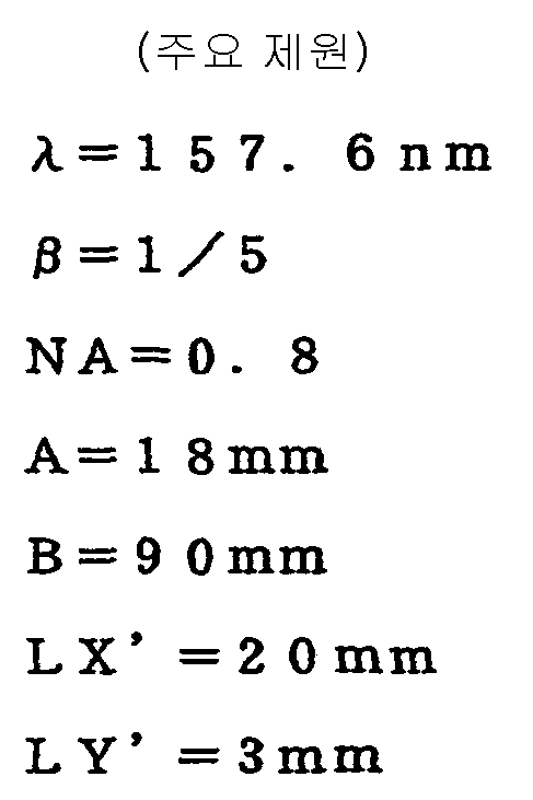
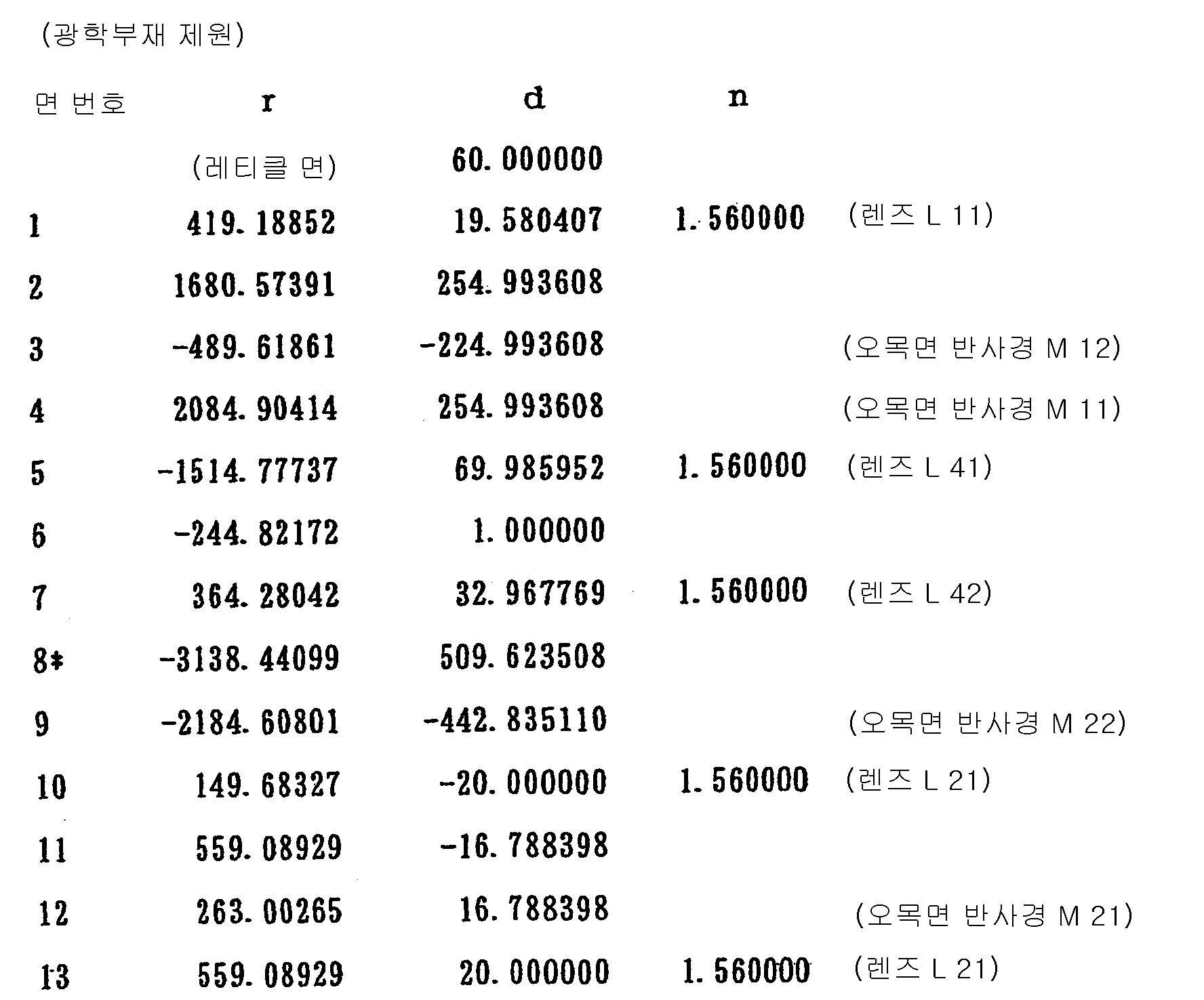
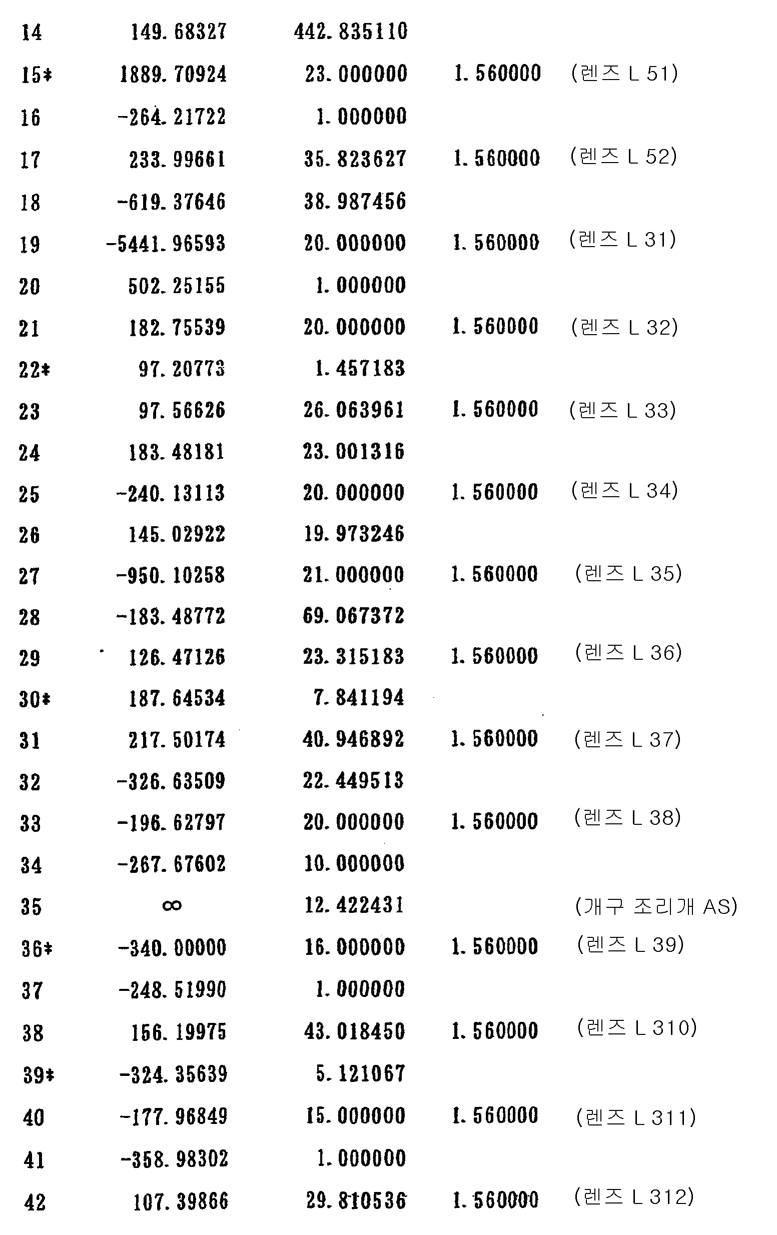
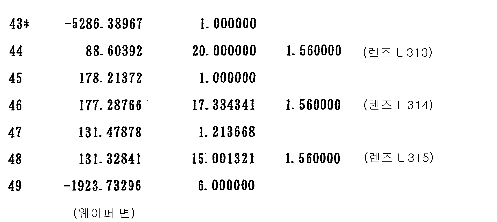
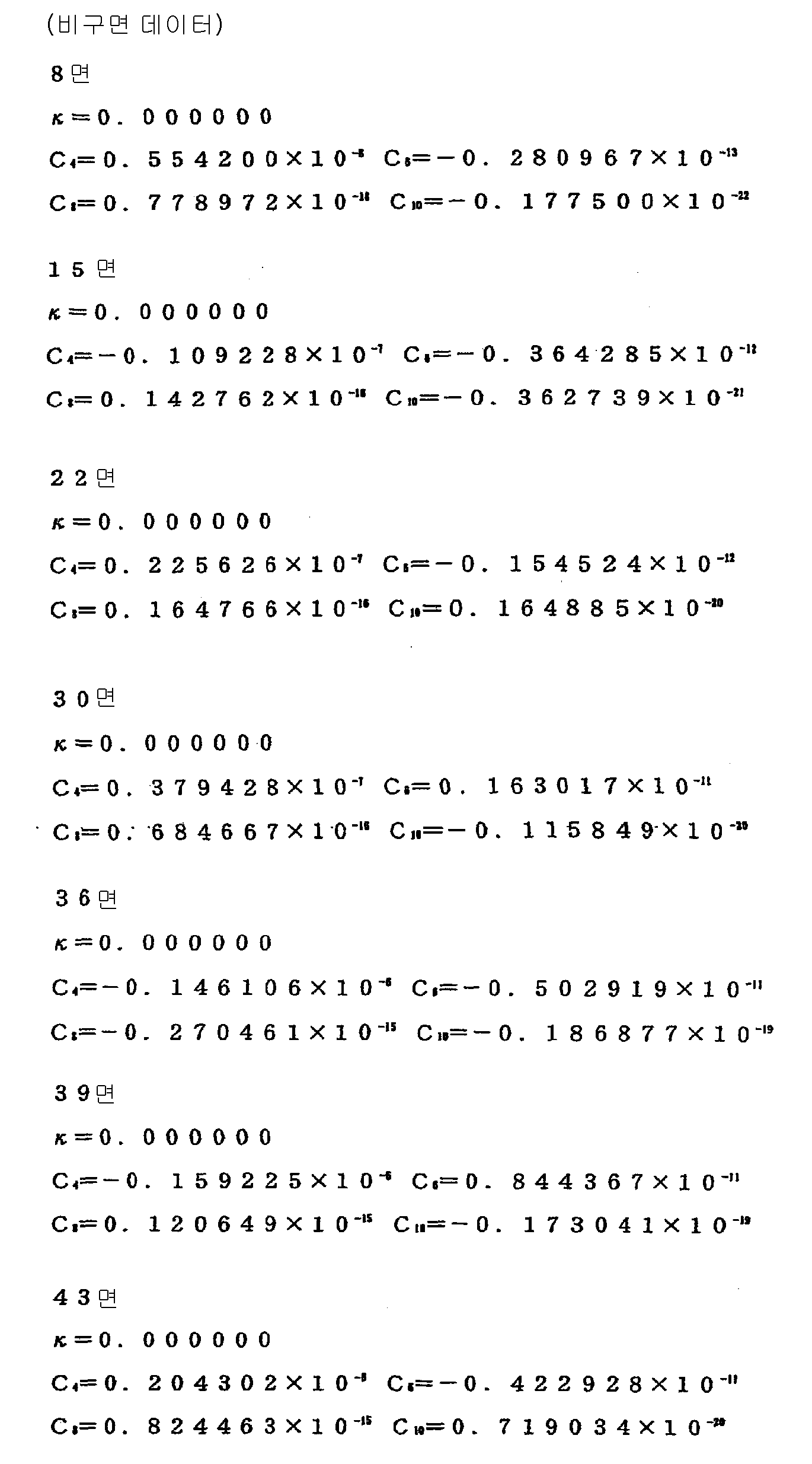
도 16은 제 6 실시예에 따른 반사굴절광학계의 가로수차를 나타내는 도면이다. 수차도에 있어서, Y는 상 높이(mm)를 나타내고 있다. 수차도로부터 명확해진 바와 같이 제 6 실시예에서도 제 3 실시예 및 제 5 실시예와 마찬가지로 파장폭이 157.6nm±0.3pm인 노광광에 대해 색수차가 양호하게 보정되어 있는 것을 알 수 있다. 또, 구면수차, 코머수차, 비점수차, 디스토션(왜곡수차)이 거의 무수차에 가까운 상태까지 양호하게 보정되고, 우수한 결상성능을 갖는 것을 확인하고 있다.Fig. 16 is a diagram showing the horizontal aberration of the reflective refractive optical system according to the sixth embodiment. In the aberration diagram, Y represents the image height (mm). As is clear from the aberration diagram, it can be seen that the chromatic aberration is well corrected for the exposure light having the wavelength width of 157.6 nm ± 0.3 pm as in the third embodiment and the fifth embodiment as well. In addition, it has been confirmed that spherical aberration, comer aberration, astigmatism and distortion (distortion aberration) are well corrected to a state almost close to aberration, and have excellent imaging performance.
(제 7 실시예)(Example 7)
도 17은 제 7 실시예에 따른 반사굴절광학계(투영광학계(PL))의 렌즈 구성을 나타내는 도면이다. 도 17의 반사굴절광학계에 있어서, 제 1 결상광학계(G1)는 레티클측으로부터 차례로, 양볼록렌즈(L11)와, 웨이퍼측에 평면에 가까운 볼록면을 향하게 한 볼록면 반사경(M11)과, 레티클측에 오목면을 향하게 오목면 반사경(M12)으로 구성되어 있다.FIG. 17 is a view showing the lens configuration of the reflective refractive optical system (projection optical system PL) according to the seventh embodiment. In the reflective refractive optical system of Fig. 17, the first imaging optical system G1 sequentially turns from the reticle side to the biconvex lens L11, the convex reflecting mirror M11 with the convex surface near the plane on the wafer side, and the reticle. It is comprised by the concave reflecting mirror M12 so that a concave surface may face to the side.
또, 제 2 결상광학계(G2)는 레티클측으로부터 차례로, 웨이퍼측으로 오목면을 향하게 한 오목면 반사경(M21)과, 레티클측으로 볼록면을 향하게 한 부 메니스커스렌즈(L21)와, 레티클측으로 오목면을 향하게 한 부 메니스커스렌즈(L22)와, 레티클측으로 오목면을 향하게 한 오목면 반사경(M22)으로 구성되어 있다.Further, the second imaging optical system G2 is concave to the concave surface facing the concave surface toward the wafer side from the reticle side, the secondary meniscus lens L21 having the convex surface facing the reticle side, and concave toward the reticle side. It consists of the sub meniscus lens L22 which faced the surface, and the concave reflecting mirror M22 which faced the concave surface toward the reticle side.
또, 제 3 결상광학계(G3)는 레티클측에서 차례로, 레티클측으로 볼록면을 향하게 한 정 메니스커스렌즈(L31)와, 레티클측으로 볼록면을 향하게 한 부 메니스커스렌즈(L32)와, 웨이퍼측에 비구면형상의 오목면을 향하게 한 정 메니스커스렌즈(L33)와, 레티클측으로 볼록면을 향하게 한 정 메니스커스렌즈(L34)와, 레티클측으로 볼록면을 향하게 한 부 메니스커스렌즈(L35)와, 레티클측으로 오목면을 향하게 한 부 메니스커스렌즈(L36)와, 웨이퍼측으로 비구면형상의 오목면을 향하게 한 정 메니스커스렌즈(L37)와, 양볼록렌즈(L38)와, 레티클측으로 오목면을 향하게 한 정 메니스커스렌즈(L39)와, 레티클측으로 오목면을 향하게 한 부 메니스커스렌즈(L310)와, 레티클측으로 비구면형상의 오목면을 향하게 한 부 메니스커스렌즈(L311)와, 레티클측으로 볼록면을 향하게 한 정 메니스커스렌즈(L312)와, 웨이퍼측의 비구면형상의 볼록면을 향하게 한 양볼록렌즈(L313) 와, 레티클측으로 오목면을 향하게 한 부 메니스커스렌즈(L314)와, 웨이퍼측으로 비구면형상의 오목면을 향하게 한 정 메니스커스렌즈(L315)와, 레티클측으로 볼록면을 향하게 한 정 메니스커스렌즈(L316)와, 레티클측으로 볼록면을 향하게 한 정 메니스커스렌즈(L317)로 구성되어 있다.In addition, the third imaging optical system G3 has a positive meniscus lens L31 having the convex surface facing the reticle side in order from the reticle side, a secondary meniscus lens L32 having the convex surface facing the reticle side, and a wafer. A positive meniscus lens L33 with an aspherical concave face on the side, a positive meniscus lens L34 with a convex face toward the reticle side, and a sub meniscus lens with a convex face toward the reticle side ( L35), the secondary meniscus lens L36 facing the concave surface toward the reticle side, the positive meniscus lens L37 facing the concave surface toward the wafer side, the biconvex lens L38, and the reticle Positive meniscus lens L39 facing the concave surface toward the side, secondary meniscus lens L310 facing the concave surface toward the reticle side, and sub meniscus lens facing the aspherical concave surface toward the reticle side (L311) ) And the convex side toward the reticle side Positive meniscus lens L312, biconvex lens L313 facing the aspherical convex surface on the wafer side, secondary meniscus lens L314 facing the concave surface toward the reticle side, and aspherical surface toward the wafer side The positive meniscus lens L315 facing the concave surface of the lens, the positive meniscus lens L316 facing the convex surface toward the reticle side, and the positive meniscus lens L317 facing the convex surface toward the reticle side. It is.
또, 제 1 결상광학계(G1)와 제 2 결상광학계(G2)의 사이의 광로 중에는 레티클측에서 차례로, 양볼록렌즈(L41)와, 웨이퍼측으로 비구면형상의 볼록면을 향하게 한 양볼록렌즈(L42)로 구성된 제 1 필드렌즈가 배치되어 있다. 또, 제 2 결상광학계(G2)와 제 3 결상광학계(G3)의 사이의 광로 중에는 레티클측으로 비구면형상의 볼록면을 향하게 한 양볼록렌즈(L51)로 구성된 제 2 필드렌즈가 배치되어 있다.In the optical path between the first imaging optical system G1 and the second imaging optical system G2, the biconvex lens L41 and the biconvex lens L42 facing the aspherical convex surface toward the wafer side in turn from the reticle side. The first field lens composed of) is arranged. Further, in the optical path between the second imaging optical system G2 and the third imaging optical system G3, a second field lens composed of biconvex lenses L51 with the aspherical convex surface facing the reticle side is disposed.
따라서, 제 7 실시예에서는 레티클(R)로부터의 광이 양볼록렌즈(L11)를 통해 오목면 반사경(M12)으로 입사한다. 오목면 반사경(M12)에서 반사된 광은 볼록면 반사경(M11)에서 반사된 후, 제 1 필드렌즈(L41 및 L42)의 근방에 레티클 패턴의 제 1 중간상을 형성한다.Therefore, in the seventh embodiment, light from the reticle R is incident on the concave reflecting mirror M12 through the biconvex lens L11. The light reflected by the concave reflector M12 is reflected by the convex reflector M11, and then forms a first intermediate image of the reticle pattern in the vicinity of the first field lenses L41 and L42.
제 1 중간상으로부터의 광은 부 메니스커스렌즈(L22)를 통해 오목면 반사경(M22)에서 반사된 후, 부 메니스커스렌즈(L22) 및 부 메니스커스렌즈(L21)를 통해 오목면 반사경(M21)에 입사한다. 오목면 반사경(M21)에서 반사된 광은 부 메니스커스렌즈(L21)를 통해 제 2 필드렌즈(L51)의 근방에 레티클 패턴의 제 2 중간상을 형성한다. 제 2 중간상으로부터의 광은 제 3 결상광학계(G3)를 구성하는 각 렌즈(L31∼L317)를 통해 웨이퍼(W)상에 레티클 패턴의 최종 상을 형성한다.The light from the first intermediate image is reflected by the concave reflector M22 through the secondary meniscus lens L22, and then the concave reflector through the secondary meniscus lens L22 and the secondary meniscus lens L21. It enters (M21). The light reflected by the concave reflector M21 forms a second intermediate image of the reticle pattern near the second field lens L51 through the sub meniscus lens L21. Light from the second intermediate image forms the final image of the reticle pattern on the wafer W through each of the lenses L31 to L317 constituting the third imaging optical system G3.
다음의 표 7에 제 7 실시예의 반사굴절광학계의 제원의 값을 든다. 표 7의 주요 제원에 있어서, λ는 노광광의 중심파장을, β는 투영배율(전체계의 결상배율)을, NA는 상측(웨이퍼측) 개구수를, A는 웨이퍼(W)상에서의 이미지 서클(IF)의 반경, 즉 최대 상 높이를, B는 최대 상 높이(A)에 대응하는 최대 물체 높이를, LX는 실효노광영역(ER)의 X방향을 따르는 치수(장변의 치수)를, LY는 실효노광영역(ER)의 Y방향을 따르른 치수(단변의 치수)를 각각 나타내고 있다.Table 7 below shows the values of the specifications of the reflective refractive optical system of the seventh embodiment. In the main specifications of Table 7, λ is the center wavelength of the exposure light, β is the projection magnification (imaging of the whole system), NA is the numerical aperture on the upper side (wafer side), and A is the image circle on the wafer W. The radius of (IF), that is, the maximum image height, B is the maximum object height corresponding to the maximum image height A, LX is the dimension along the X direction of the effective exposure area ER (the long side dimension), LY Denotes the dimensions (dimensions of the short sides) along the Y direction of the effective exposure area ER, respectively.
또, 표 7의 광학부재 제원에 있어서, 제 1 컬럼의 면 번호는 레티클측으로부터의 면의 순서를, 제 2 컬럼의 r은 각 면의 곡률반경(비구면의 경우에는 정점곡률반경:mm)을, 제 3 컬럼의 d는 각 면의 축상간격, 즉 면간격(mm)을, 제 4 컬럼의 n은 중심파장에 대한 굴절율을 각각 나타내고 있다. 또, 면간격(d)은 반사될 때마다 그 부호를 바꾸는 것으로 한다. 따라서, 면간격(d)의 부호는 오목면 반사경(M12)으로부터 오목면 반사경(M11)으로의 광로 중 및 오목면 반사경(M22)으로부터 오목면 반사경(M21)으로의 광로 중에서는 부로 하고, 그 외의 광로 중에서는 정으로 하고 있다. 또, 광의 입사방향에 상관없이 레티클측을 향해 볼록면의 곡률반경을 정으로 하고, 레티클측을 향해 오목면의 곡률반경을 부로 하고 있다. 또, 표 7의 조건식 대응값에 있어서, LAT는 배율색수차계수를, AX는 축상색수차계 수를 각각 나타내고 있다.In addition, in the optical member specifications of Table 7, the surface number of the first column is the order of the surface from the reticle side, and the r of the second column is the radius of curvature of each surface (vertical radius of curvature: mm). , D in the third column represents the axial spacing of each surface, that is, the surface spacing (mm), and n in the fourth column represents the refractive index with respect to the center wavelength. It is to be noted that the plane interval d changes its sign every time it is reflected. Therefore, the sign of the surface interval d is negative in the optical path from the concave reflector M12 to the concave reflector M11 and in the optical path from the concave reflector M22 to the concave reflector M21, In other light paths, it is set as positive. In addition, the radius of curvature of the convex surface is set toward the reticle side regardless of the incident direction of light, and the radius of curvature of the concave surface is made negative toward the reticle side. In the conditional expression corresponding value shown in Table 7, LAT represents the magnification chromatic aberration coefficient, and AX represents the axial chromatic aberration coefficient, respectively.
(표 7)Table 7
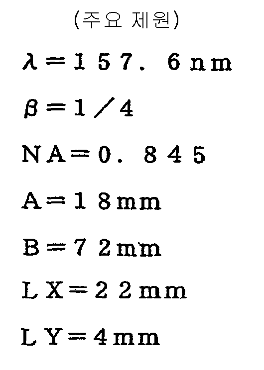
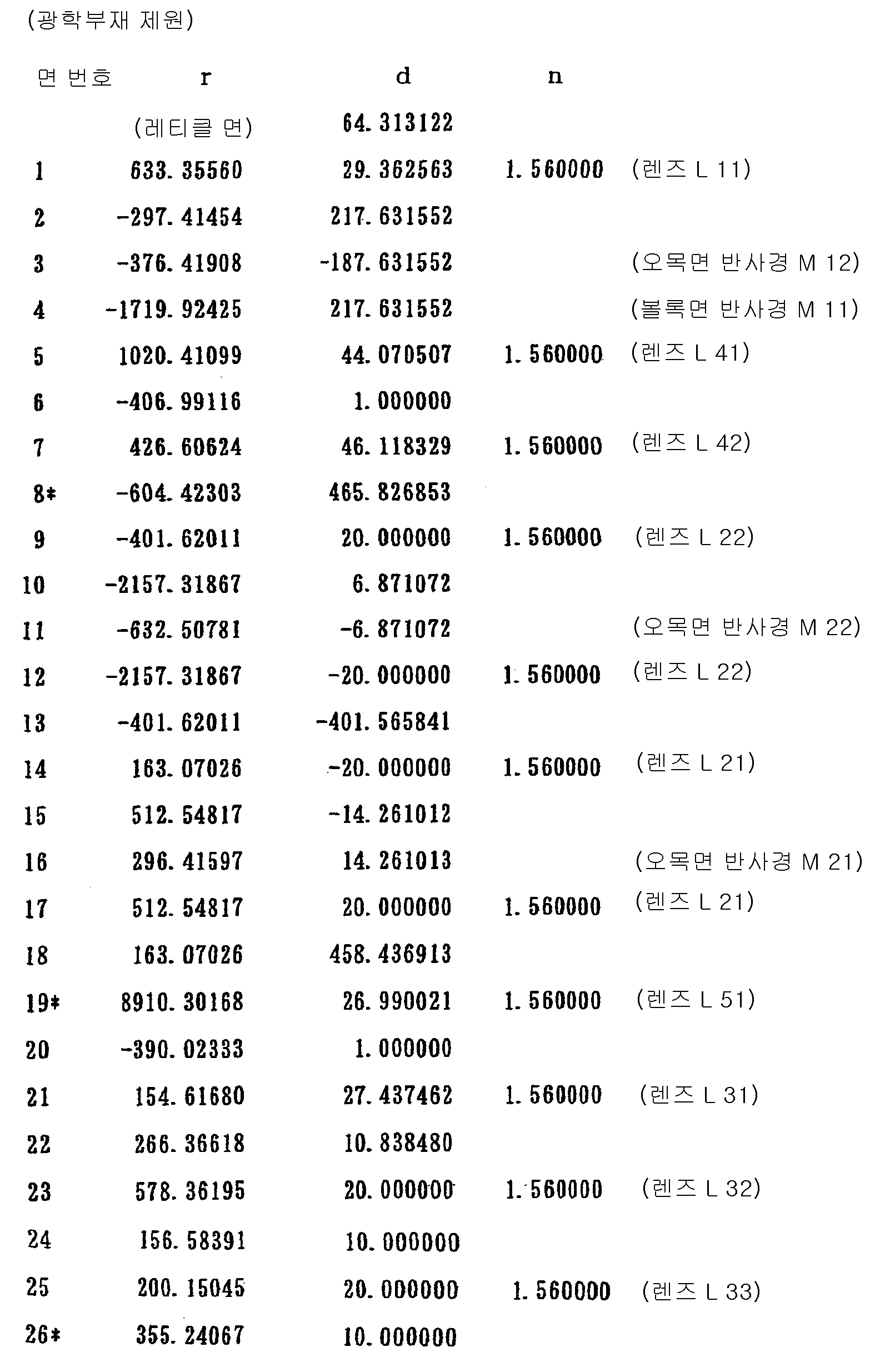
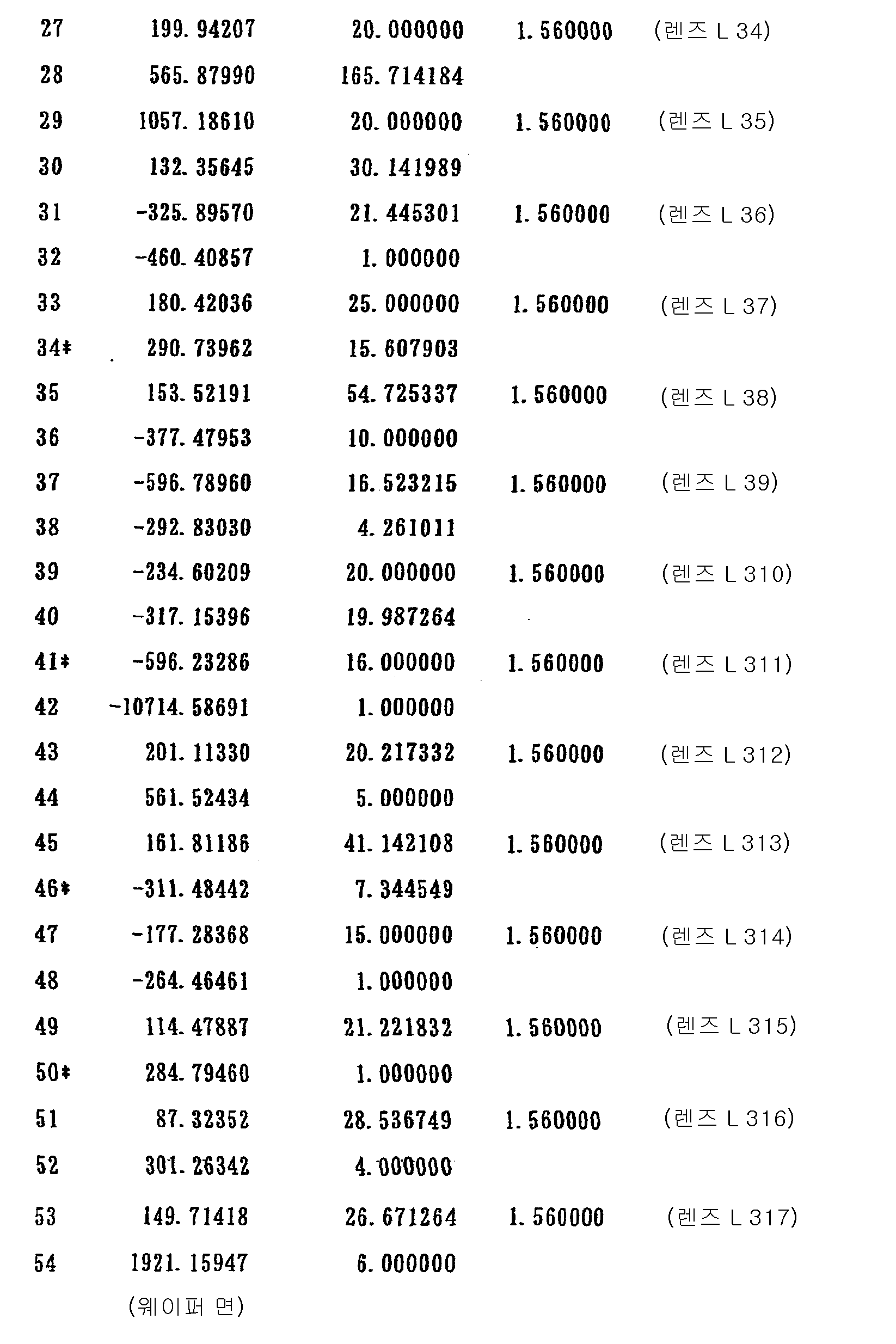
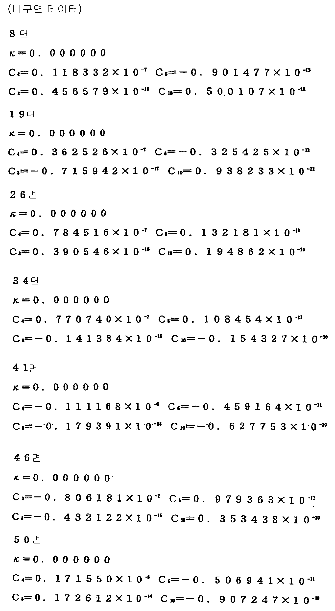
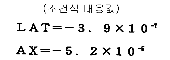
도 18 및 도 19는 제 7 실시예에 따른 반사굴절광학계의 가로수차를 나타내는 도면이다. 수차도에 있어서, Y는 상 높이(mm)를 나타내고 있다. 수차도로부터 명확해진 바와 같이, 제 7 실시예에서는 파장폭이 157.6nm±0.4pm의 노광광에 대해 색수차가 양호하게 보정되는 것을 알 수 있다. 또, 구면수차, 코머수차, 비점수차, 디스토션(왜곡수차)이 거의 무수차에 가까운 상태까지 양호하게 보정되고, 우수한 결상성능을 갖는 것이 확인되고 있다.18 and 19 are diagrams showing lateral aberrations of the reflective refractive optical system according to the seventh embodiment. In the aberration diagram, Y represents the image height (mm). As is clear from the aberration diagram, it can be seen that in the seventh embodiment, chromatic aberration is well corrected for exposure light having a wavelength width of 157.6 nm ± 0.4 pm. In addition, it has been confirmed that spherical aberration, comer aberration, astigmatism, and distortion (distortion aberration) are well corrected to a state almost close to aberration, and have excellent imaging performance.
(제 8 실시예)(Example 8)
도 20은 제 8 실시예에 따른 반사굴절광학계(투영광학계(PL))의 렌즈 구성을 나타내는 도면이다. 도 20의 반사굴절광학계에 있어서, 제 1 결상광학계(G1)는 레티클측으로부터 차례로, 양볼록렌즈(L11)와, 웨이퍼측으로 평면에 가까운 볼록면을 향하게 한 볼록면 반사경(M11)과, 레티클측으로 오목면을 향하게 오목면 반사경(M12)으로 구성되어 있다.20 is a diagram showing a lens configuration of a reflection refractive optical system (projection optical system PL) according to the eighth embodiment. In the reflective refractive optical system shown in Fig. 20, the first imaging optical system G1 sequentially moves from the reticle side to the biconvex lens L11, the convex reflector M11 with the convex surface near the plane toward the wafer side, and the reticle side. It is comprised by the concave reflecting mirror M12 toward a concave surface.
또, 제 2 결상광학계(G2)는 레티클측으로부터 차례로, 웨이퍼측으로 오목면을 향하게 한 오목면 반사경(M21)과, 레티클측으로 볼록면을 향하게 한 부 메니스커스렌즈(L21)와, 레티클측으로 오목면을 향하게 한 부 메니스커스렌즈(L22)와, 레티클측으로 오목면을 향하게 한 오목면 반사경(M22)으로 구성되어 있다.Further, the second imaging optical system G2 is concave to the concave surface facing the concave surface toward the wafer side from the reticle side, the secondary meniscus lens L21 having the convex surface facing the reticle side, and concave toward the reticle side. It consists of the sub meniscus lens L22 which faced the surface, and the concave reflecting mirror M22 which faced the concave surface toward the reticle side.
또, 제 3 결상광학계(G3)는 레티클측에서 차례로, 레티클측으로 오목면을 향하게 한 부 메니스커스렌즈(L31)와, 레티클측으로 볼록면을 향하게 한 부 메니스커스렌즈(L32)와, 양볼록렌즈(L33)와, 웨이퍼측에 비구면형상의 오목면을 향하게 한 부 메니스커스렌즈(L34)와, 양오목렌즈(L35)와, 레티클측으로 오목면을 향하게 한 부 메니커스렌즈(L36)와, 웨이퍼측으로 비구면형상의 오목면을 향하게 한 정 메니스커스렌즈(L37)와, 양볼록렌즈(L38)와, 레티클측으로 오목면을 향하게 한 정 메니스커스렌즈(L39)와, 레티클측으로 오목면을 향하게 한 부 메니스커스렌즈(L310)와, 레티클측으로 비구면형상의 오목면을 향하게 한 부 메니스커스렌즈(L311)와, 레티클측으로 볼록면을 향하게 한 정 메니스커스렌즈(L312)와, 웨이퍼측의 비구면형상의 볼록면을 향하게 한 양볼록렌즈(L313)와, 레티클측으로 오목면을 향하게 한 부 메니스커스렌즈(L314)와, 웨이퍼측으로 비구면형상의 오목면을 향하게 한 정 메니스커스렌즈(L315)와, 레티클측으로 볼록면을 향하게 한 정 메니스커스렌즈(L316)와, 레티클측으로 볼록면을 향하게 한 정 메니스커스렌즈(L317)로 구성되어 있다.In addition, the third imaging optical system G3 includes, in order from the reticle side, the sub meniscus lens L31 facing the concave surface toward the reticle side, the sub meniscus lens L32 facing the convex surface toward the reticle side, and both. Convex lens L33, secondary meniscus lens L34 facing the aspherical concave surface on the wafer side, biconcave lens L35, secondary meniscus lens L36 facing the concave surface toward the reticle side The positive meniscus lens L37 faces the aspherical concave surface toward the wafer side, the biconvex lens L38, the positive meniscus lens L39 faces the concave surface toward the reticle side, and concave toward the reticle side. The sub meniscus lens L310 facing the surface, the sub meniscus lens L311 facing the concave surface toward the reticle side, and the positive meniscus lens L312 facing the convex surface toward the reticle side; Double convex lene facing the aspherical convex surface on the wafer side (L313), the secondary meniscus lens L314 facing the concave surface toward the reticle side, the positive meniscus lens L315 facing the concave surface toward the wafer side, and the tablet facing the convex surface toward the reticle side. The meniscus lens L316 and the positive meniscus lens L317 which faced the convex surface toward the reticle side are comprised.
또, 제 1 결상광학계(G1)와 제 2 결상광학계(G2) 사이의 광로 중에는 레티클측으로부터 차례로, 양볼록렌즈(L41)와, 웨이퍼측으로 비구면형상의 볼록면을 향하게 한 양볼록렌즈(L42)로 구성된 제 1 필드렌즈가 배치되어 있다. 또, 제 2 결상광학계(G2)와 제 3 결상광학계(G3)의 사이의 광로 중에는 레티클측으로 비구면형상의 오목면을 향하게 한 정 메니스커스렌즈(L51)로 구성된 제 2 필드렌즈가 배치되어 있다.In addition, in the optical path between the first imaging optical system G1 and the second imaging optical system G2, the biconvex lens L41 and the biconvex lens L42 facing the aspherical convex surface toward the wafer side in turn from the reticle side. A first field lens composed of Further, in the optical path between the second imaging optical system G2 and the third imaging optical system G3, a second field lens composed of the positive meniscus lens L51 with the aspherical concave surface facing the reticle side is disposed. .
따라서, 제 8 실시예에서는 레티클(R)로부터의 광이 양볼록렌즈(L11)를 통해 오목면 반사경(M12)으로 입사된다. 오목면 반사경(M12)에서 반사된 광은 볼록면 반사경(M11)에서 반사된 후, 제 1 필드렌즈(L41 및 L42)의 근방에 레티클 패턴의 제 1 중간상을 형성한다.Therefore, in the eighth embodiment, light from the reticle R is incident on the concave reflecting mirror M12 through the biconvex lens L11. The light reflected by the concave reflector M12 is reflected by the convex reflector M11, and then forms a first intermediate image of the reticle pattern in the vicinity of the first field lenses L41 and L42.
제 1 중간상으로부터의 광은 부 메니스커스렌즈(L22)를 통해 오목면 반사경(M22)으로 반사된 후, 부 메니스커스렌즈(L22) 및 부 메니스커스렌즈(L21)를 통해 오목면 반사경(M21)으로 입사된다. 오목면 반사경(M21)에서 반사된 광은 부 메니스커스렌즈(L21)를 통해 제 2 필드렌즈(L51)의 근방에 레티클 패턴의 제 2 중간상을 형성한다. 제 2 중간상으로부터의 광은 제 3 결상광학계(G3)를 구성하는 각 렌즈(L31∼L317)를 통해 웨이퍼(W)상에 레티클 패턴의 최종 상을 형성한다.The light from the first intermediate image is reflected through the secondary meniscus lens L22 to the concave reflector M22, and then through the secondary meniscus lens L22 and the secondary meniscus lens L21. It enters into M21. The light reflected by the concave reflector M21 forms a second intermediate image of the reticle pattern near the second field lens L51 through the sub meniscus lens L21. Light from the second intermediate image forms the final image of the reticle pattern on the wafer W through each of the lenses L31 to L317 constituting the third imaging optical system G3.
다음의 표 8에 제 8 실시예의 반사굴절광학계의 제원의 값을 든다. 표 8의 주요 제원에 있어서, λ은 노광광의 중심파장을, β는 투영배율(전체계의 결상배율)을, NA는 상측(웨이퍼측) 개구수를, A는 웨이퍼(W)상에서의 이미지 서클(IF)의 반경, 즉 최대 상 높이를, B는 최대 상 높이(A)에 대응하는 최대 물체 높이를, LX는 실효노광영역(ER)의 X방향을 따르는 치수(장변의 치수)를, LY는 실효노광영역(ER)의 Y방향을 따르른 치수(단변의 치수)를 각각 나타내고 있다.Table 8 below shows the values of the specifications of the reflective refractive optical system of the eighth embodiment. In the main specifications of Table 8, λ is the center wavelength of the exposure light, β is the projection magnification (image-forming magnification of the entire system), NA is the numerical aperture on the upper side (wafer side), and A is the image circle on the wafer W. The radius of (IF), that is, the maximum image height, B is the maximum object height corresponding to the maximum image height A, LX is the dimension along the X direction of the effective exposure area ER (the long side dimension), LY Denotes the dimensions (dimensions of the short sides) along the Y direction of the effective exposure area ER, respectively.
또, 표 8의 광학부재 제원에 있어서, 제 1 컬럼의 면 번호는 레티클측으로부터의 면의 순서를, 제 2 컬럼의 r은 각 면의 곡률반경(비구면의 경우에는 정점곡률반경:mm)을, 제 3 컬럼의 d는 각 면의 축상간격, 즉 면간격(mm)을, 제 4 컬럼의 n은 중심파장에 대한 굴절율을 각각 나타내고 있다. 또, 면간격(d)은 반사될 때마다 그 부호를 바꾸는 것으로 한다. 따라서, 면간격(d)의 부호는 오목면 반사경(M12)으로부터 오목면 반사경(M11)으로의 광로 중 및 오목면 반사경(M22)으로부터 오목면 반사경(M21)으로의 광로 중에서는 부로 하고, 그 외의 광로 중에서는 정으로 하고 있다. 또, 광의 입사방향에 상관없이 레티클측을 향해 볼록면의 곡률반경을 정으로 하고, 레티클측을 향해 오목면의 곡률반경을 부로 하고 있다. 또, 표 8의 조건식 대응값에 있어서, LAT는 배율색수차계수를, AX는 축상색수차계수를 각각 나타내고 있다.In the optical member specifications of Table 8, the surface number of the first column is the order of the surface from the reticle side, and the r of the second column is the radius of curvature of each surface (vertical radius of curvature: mm). , D in the third column represents the axial spacing of each surface, that is, the surface spacing (mm), and n in the fourth column represents the refractive index with respect to the center wavelength. It is to be noted that the plane interval d changes its sign every time it is reflected. Therefore, the sign of the surface interval d is negative in the optical path from the concave reflector M12 to the concave reflector M11 and in the optical path from the concave reflector M22 to the concave reflector M21, In other light paths, it is set as positive. In addition, the radius of curvature of the convex surface is set toward the reticle side regardless of the incident direction of light, and the radius of curvature of the concave surface is made negative toward the reticle side. In Table 8, LAT represents a magnification chromatic aberration coefficient, and AX represents an axial chromatic aberration coefficient.
(표 8)Table 8
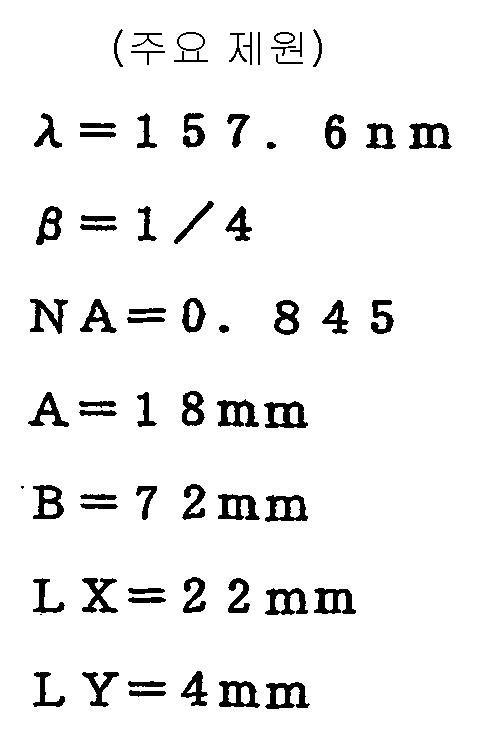

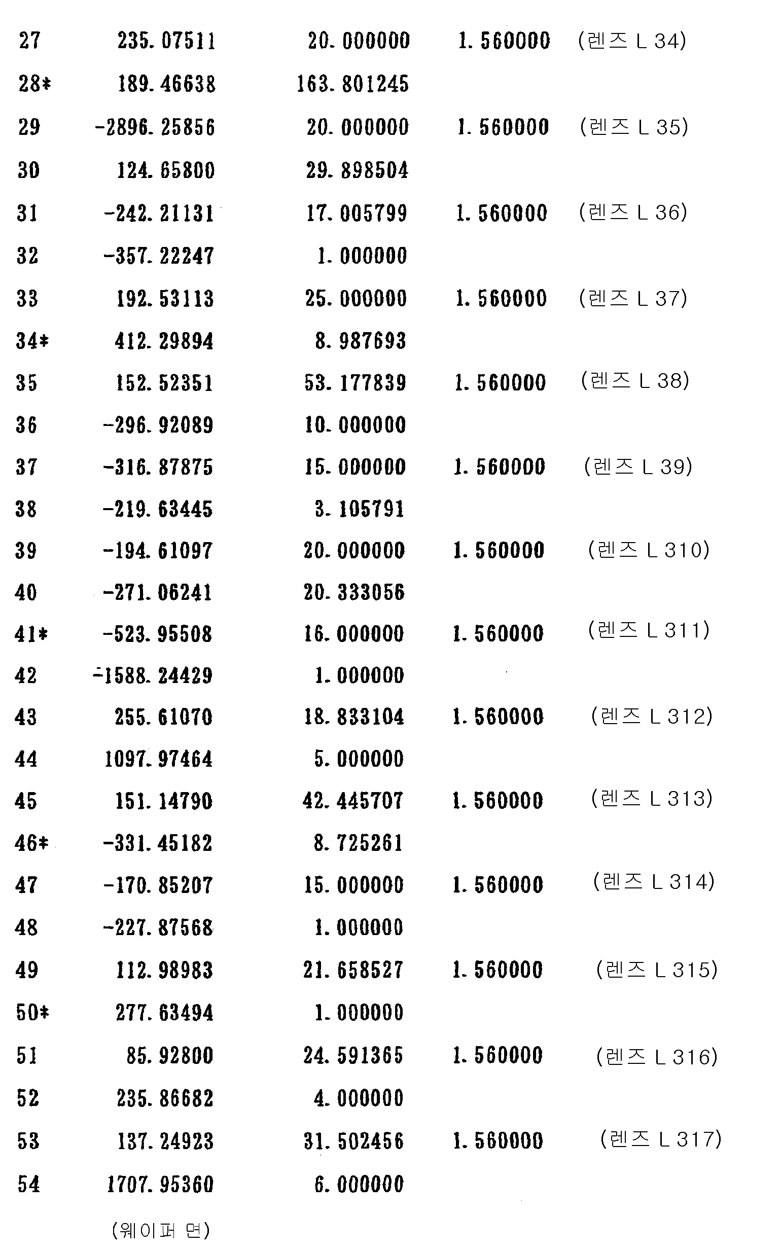
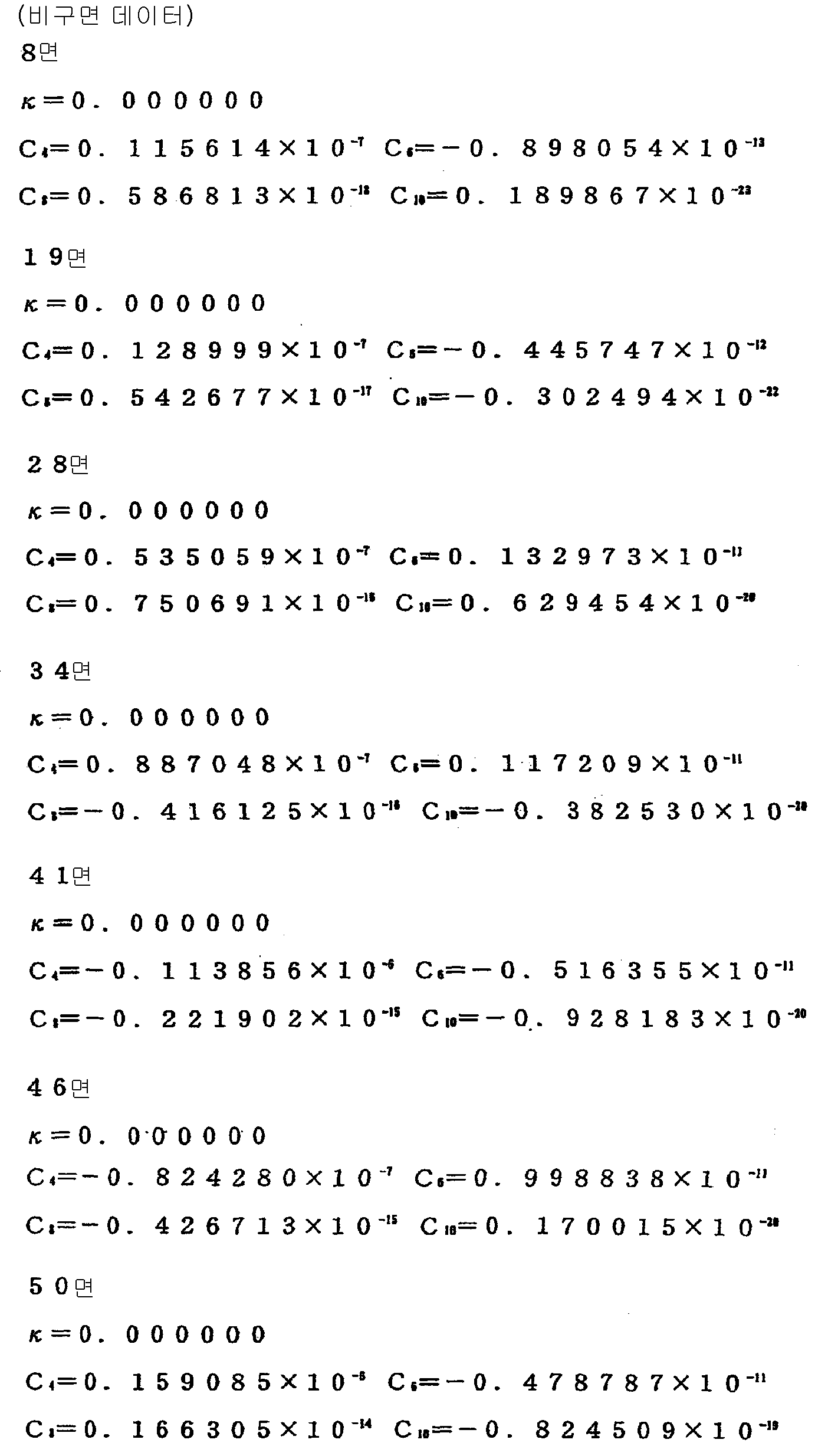
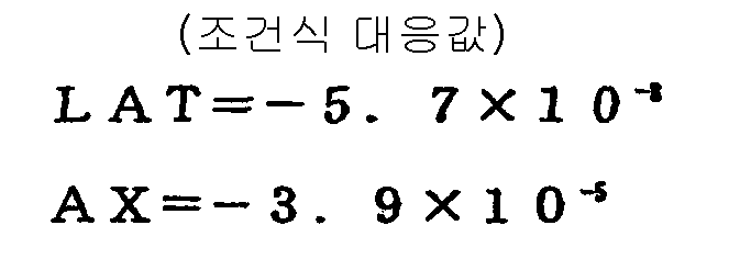
도 21 및 도 22는 제 8 실시예에 따른 반사굴절광학계의 가로수차를 나타내는 도면이다. 수차도에 있어서, Y는 상 높이(mm)를 나타내고 있다. 수차도로부터 명확해진 바와 같이, 제 8 실시예에서는 제 7 실시예와 마찬가지로 파장 폭이 157.6nm±0.4pm인 노광광에 대해 색수차가 양호하게 보정되는 것을 알 수 있다. 또, 구면수차, 코머수차, 비점수차, 디스토션(왜곡 수차)이 거의 무수차에 가까운 상태까지 양호하게 보정되고, 우수한 결상성능을 갖는 것이 확인되고 있다.21 and 22 are diagrams showing lateral aberration of the reflective refractive optical system according to the eighth embodiment. In the aberration diagram, Y represents the image height (mm). As apparent from the aberration diagram, it can be seen that in the eighth embodiment, similarly to the seventh embodiment, chromatic aberration is well corrected for exposure light having a wavelength width of 157.6 nm ± 0.4 pm. In addition, it has been confirmed that spherical aberration, comer aberration, astigmatism, and distortion (distortion aberration) are well corrected to a state almost close to aberration, and have excellent imaging performance.
(제 9 실시예)(Example 9)
도 23은 제 9 실시예에 따른 반사굴절광학계(투영광학계(PL))의 렌즈 구성을 나타내는 도면이다. 도 23의 반사굴절광학계에 있어서, 제 1 결상광학계(G1)는 레티클측으로부터 차례로, 양볼록렌즈(L11)와, 웨이퍼측에 평면에 가까운 볼록면을 향하게 한 볼록면 반사경(M11)과, 레티클측에 오목면을 향하게 한 부 메니스커스렌즈(L12)와, 레티클측으로 오목면을 향하게 한 오목면 반사경(M12)으로 구성되어 있다.FIG. 23 is a diagram showing a lens configuration of a reflection refractive optical system (projection optical system PL) according to the ninth embodiment. In the reflection refractive optical system shown in Fig. 23, the first imaging optical system G1 sequentially turns from the reticle side to the biconvex lens L11, the convex reflecting mirror M11 facing the plane near the plane on the wafer side, and the reticle. It consists of the sub meniscus lens L12 which made the concave surface facing the side, and the concave reflecting mirror M12 which made the concave surface facing the reticle side.
또, 제 2 결상광학계(G2)는 레티클측으로부터 차례로, 웨이퍼측으로 오목면을 향하게 한 오목면 반사경(M21)과, 레티클측으로 볼록면을 향하게 한 부 메니스커스렌즈(L21)와, 레티클측으로 평면에 가까운 오목면을 향하게 한 오목면 반사경(M22)으로 구성되어 있다.In addition, the second imaging optical system G2 has a concave reflecting mirror M21 with the concave surface facing the wafer side in turn from the reticle side, a sub meniscus lens L21 having the convex surface facing the reticle side, and a plane toward the reticle side. It is comprised by the concave reflecting mirror M22 which faced the concave surface near.
또, 제 3 결상광학계(G3)는 레티클측으로부터 차례로, 양볼록렌즈(L31)와, 웨이퍼측으로 비구면형상의 오목면을 향하게 한 양오목렌즈(L32)와, 레티클측으로 볼록면을 향하게 한 정 메니스커스렌즈(L33)와, 양오목렌즈(L34)와, 레티클측으로 볼록면을 향하게 한 부 메니스커스렌즈(L35)와, 웨이퍼측으로 비구면 형상의 오목면을 향하게 한 정 메니스커스렌즈(L36)와, 양볼록렌즈(L37)와, 레티클측으로 오목면을 향하게 한 정 메니스커스렌즈(L38)와, 레티클측으로 비구면형상의 오목면을 향하게 한 양오목렌즈(L39)와, 양볼록렌즈(L310)와, 웨이퍼측으로 비구면형상의 볼록면을 향하게 한 양볼록렌즈(L311)와, 레티클측으로 오목면을 향하게 한 부 메니스커스렌즈(L312)와, 웨이퍼측의 비구면형상의 오목면을 향하게 한 정 메니스커스렌즈(L313)와, 레티클측으로 볼록면을 향하게 한 정 메니스커스렌즈(L314)와, 레티클측으로 볼록면을 향하게 한 정 메니스커스렌즈(L315)로 구성되어 있다.In addition, the third imaging optical system G3 has, in order from the reticle side, the biconvex lens L31, the biconvex lens L32 facing the aspherical concave surface toward the wafer side, and the positive convex surface facing the convex surface toward the reticle side. A varnish lens L33, a bispherical lens L34, a sub meniscus lens L35 facing the convex side toward the reticle side, and a positive meniscus lens L36 facing the aspherical concave surface toward the wafer side. ), A biconvex lens L37, a positive meniscus lens L38 facing the concave surface toward the reticle side, a biconvex lens L39 facing the concave surface toward the reticle side, and a biconvex lens ( L310, the biconvex lens L311 facing the aspherical convex surface toward the wafer side, the sub meniscus lens L312 facing the concave surface toward the reticle side, and the aspherical concave surface facing the wafer side. Positive meniscus lens (L313) and the convex surface toward the reticle side. It is composed of a positive meniscus lens (L314), and a positive meniscus lens (L315) a convex surface facing the reticle side.
또, 제 1 결상광학계(G1)와 제 2 결상광학계(G2)의 사이의 광로 중에는 레티클측으로부터 차례로, 양볼록렌즈(L41)와, 웨이퍼측으로 비구면형상의 볼록면을 향하게 한 양볼록렌즈(L42)로 구성된 제 1 필드렌즈가 배치되어 있다. 또, 제 2 결상광학계(G2)와 제 3 결상광학계(G3)의 사이의 광로 중에는 레티클측으로 비구면형상의 오목면을 향하게 한 정 메니스커스렌즈(L51)와, 레티클측으로 오목면을 향하게 한 정 메니스커스렌즈(L52)로 구성된 제 2 필드렌즈가 배치되어 있다.Moreover, in the optical path between the first imaging optical system G1 and the second imaging optical system G2, the biconvex lens L41 and the biconvex lens L42 facing the aspherical convex surface toward the wafer side in turn from the reticle side. The first field lens composed of) is arranged. In addition, among the optical paths between the second imaging optical system G2 and the third imaging optical system G3, the positive meniscus lens L51 having the aspherical concave surface toward the reticle side and the tablet facing the concave surface toward the reticle side A second field lens composed of the meniscus lenses L52 is disposed.
따라서, 제 9 실시예에서는 레티클(R)로부터의 광이 양볼록렌즈(L11) 및 부 메니스커스렌즈(L12)를 통해 오목면 반사경(M12)으로 입사한다. 오목면 반사경(M12)에서 반사된 광은 볼록면 반사경(M11)에서 반사된 후, 제 1 필드 렌즈(L41 및 L42)의 근방에 레티클 패턴의 제 1 중간상을 형성한다.Therefore, in the ninth embodiment, light from the reticle R is incident on the concave reflecting mirror M12 through the biconvex lens L11 and the secondary meniscus lens L12. The light reflected by the concave reflector M12 is reflected by the convex reflector M11, and then forms a first intermediate image of the reticle pattern in the vicinity of the first field lenses L41 and L42.
제 1 중간상으로부터의 광은 오목면 반사경(M22)에서 반사된 후, 부 메니스커스렌즈(L21)를 통해 오목면 반사경(M21)으로 입사한다. 오목면 반사경(M21)에서 반사된 광은 부 메니스커스렌즈(L21)를 통해 제 2 필드렌즈(L51 및 L52)의 근방에 레티클 패턴의 제 2 중간상을 형성한다. 제 2 중간상으로부터의 광은 제 3 결상광학계(G3)를 구성하는 각 렌즈(L31∼L315)를 통해 웨이퍼(W)상에 레티클 패턴의 최종 상을 형성한다.Light from the first intermediate image is reflected by the concave reflector M22 and then enters the concave reflector M21 through the sub meniscus lens L21. The light reflected by the concave reflector M21 forms a second intermediate image of the reticle pattern in the vicinity of the second field lenses L51 and L52 through the sub meniscus lens L21. Light from the second intermediate image forms a final image of the reticle pattern on the wafer W through each of the lenses L31 to L315 constituting the third imaging optical system G3.
다음의 표 9에 제 9 실시예의 반사굴절광학계의 제원의 값을 든다. 표 9의 주요 제원에 있어서, λ는 노광광의 중심파장을, β는 투영배율(전체계의 결상배율)을, NA는 상측(웨이퍼측) 개구수를, A는 웨이퍼(W)상에서의 이미지 서클(IF)의 반경, 즉 최대 상 높이를, B는 최대 상 높이(A)에 대응하는 최대 물체 높이를, LX는 실효노광영역(ER)의 X방향을 따르는 치수(장변의 치수)를, LY는 실효노광영역(ER)의 Y방향을 따르는 치수(단변의 치수)를 각각 나타내고 있다.Table 9 below shows the values of the specifications of the reflective refractive optical system of the ninth embodiment. In the main specifications of Table 9, λ is the center wavelength of the exposure light, β is the projection magnification (image-forming magnification of the entire system), NA is the numerical aperture on the upper side (wafer side), and A is the image circle on the wafer W. The radius of (IF), that is, the maximum image height, B is the maximum object height corresponding to the maximum image height A, LX is the dimension along the X direction of the effective exposure area ER (the long side dimension), LY Denotes dimensions (short side dimensions) along the Y direction of the effective exposure region ER, respectively.
또, 표 9의 광학부재 제원에 있어서, 제 1 컬럼의 면 번호는 레티클측으로부터의 면의 순서를, 제 2 컬럼의 r은 각 면의 곡률반경(비구면의 경우에는 정점곡률반경:mm)을, 제 3 컬럼의 d는 각 면의 축상간격, 즉 면간격(mm)을, 제 4 컬럼의 n은 중심파장에 대한 굴절율을 각각 나타내고 있다. 또, 면 간격(d)은 반사될 때마다 그 부호를 바꾸는 것으로 한다. 따라서, 면 간격(d)의 부호는 오목면 반사경(M12)으로부터 오목면 반사경(M11)으로의 광로 중 및 오목면 반사경(M22)으로부터 오목면 반사경(M21)으로의 광로 중에서는 부로 하고, 그 외의 광로 중에서는 정으로 하고 있다. 또, 광의 입사방향에 상관없이 레티클측을 향해 볼록면의 곡률반경을 정으로 하고, 레티클측을 향해 오목면의 곡률반경을 부로 하고 있다. 또, 표 9의 조건식 대응값에 있어서, LAT는 배율색수차계수를, AX는 축상색수차계 수를 각각 나타내고 있다.In the optical member specifications of Table 9, the surface number of the first column is the order of the surfaces from the reticle side, and the r of the second column is the radius of curvature of the respective surfaces (vertical radius of curvature: mm in the case of aspherical surfaces). , D in the third column represents the axial spacing of each surface, that is, the surface spacing (mm), and n in the fourth column represents the refractive index with respect to the center wavelength. It is to be noted that the surface spacing d changes its sign every time it is reflected. Therefore, the sign of the surface spacing d is negative in the optical path from the concave reflector M12 to the concave reflector M11 and in the optical path from the concave reflector M22 to the concave reflector M21, In other light paths, it is set as positive. In addition, the radius of curvature of the convex surface is set toward the reticle side regardless of the incident direction of light, and the radius of curvature of the concave surface is made negative toward the reticle side. In Table 9, LAT represents a magnification chromatic aberration coefficient, and AX represents an axial chromatic aberration coefficient.
(표 9)Table 9
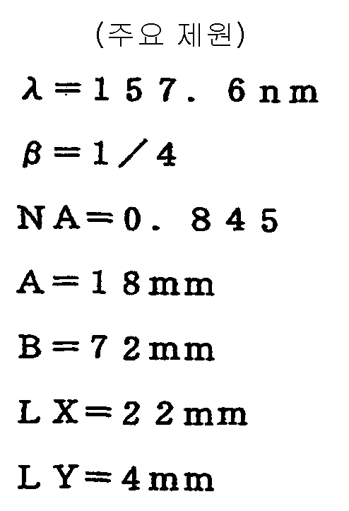

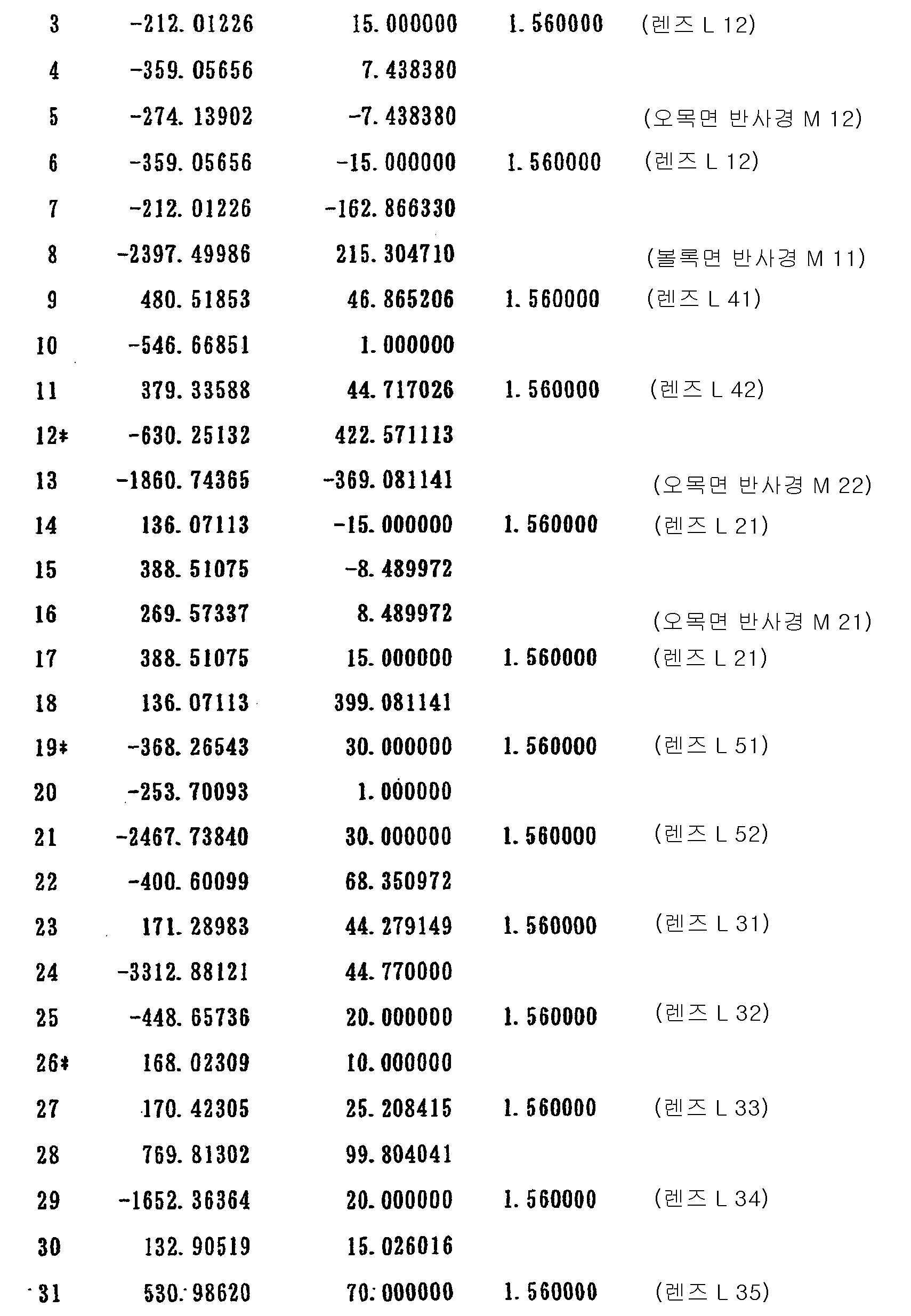

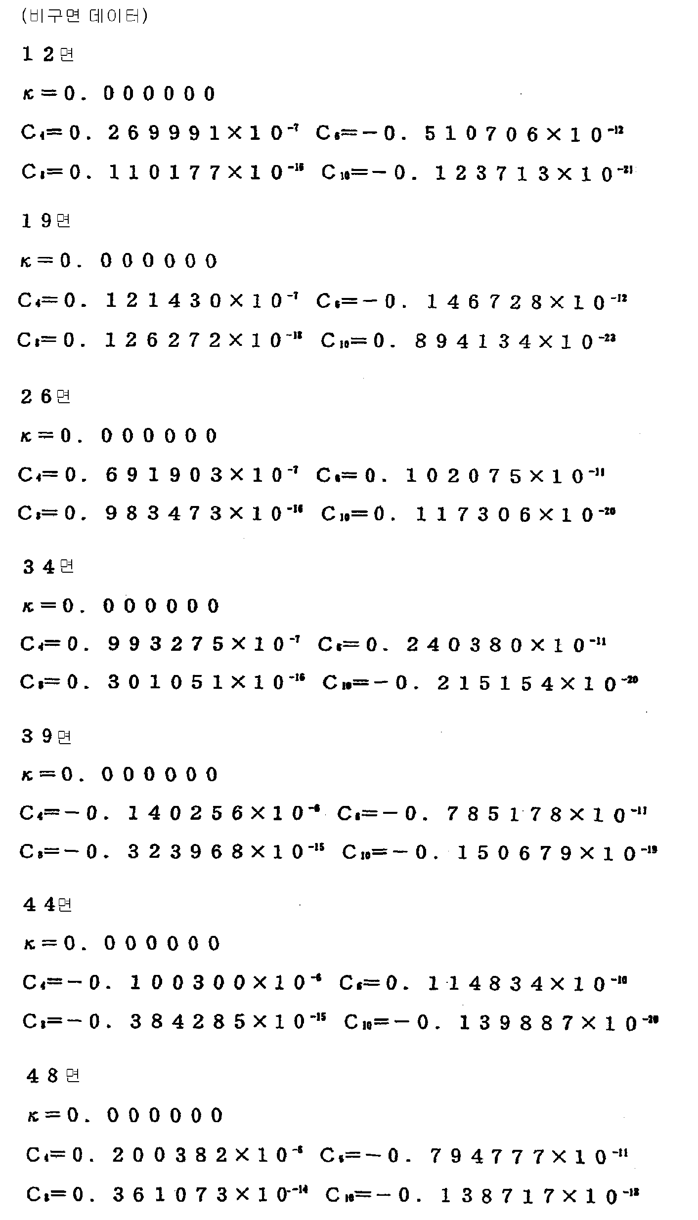

도 24 및 도 25는 제 9 실시예에 따른 반사굴절광학계의 가로수차를 나타내는 도면이다. 수차도에 있어서, Y는 상 높이(mm)를 나타내고 있다. 수차도로부터 명확해진 바와 같이, 제 9 실시예에 있어서는 제 7 실시예 및 제 8 실시예와 마찬가지로 파장폭이 157.6nm±0.4pm인 노광광에 대해 색수차가 양호하게 보정되는 것을 알 수 있다. 또, 구면수차, 코머수차, 비점수차, 디스토션(왜곡수차)이 거의 무수차에 가까운 상태까지 양호하게 보정되고, 우수한 결상성능을 갖는 것이 확인되고 있다.24 and 25 are diagrams showing lateral aberration of the reflective refractive optical system according to the ninth embodiment. In the aberration diagram, Y represents the image height (mm). As is clear from the aberration diagram, it can be seen that in the ninth embodiment, similarly to the seventh and eighth embodiments, chromatic aberration is well corrected for exposure light having a wavelength width of 157.6 nm ± 0.4 pm. In addition, it has been confirmed that spherical aberration, comer aberration, astigmatism, and distortion (distortion aberration) are well corrected to a state almost close to aberration, and have excellent imaging performance.
이상과 같이, 제 1 실시예에서는 중심파장이 157.6nm의 F2 레이저광에 대해 0.7의 상 측 NA를 확보하고 또, 웨이퍼(W)상에서 색수차를 비롯한 제수차가 충분히 보정된 반경이 17mm의 이미지 서클을 확보할 수 있다. 한편, 제 2 실시예에서는 중심 파장이 157.6nm의 F2 레이저광에 대해 0.8의 상 측 NA를 확보하고 또, 웨이퍼(W)상에서 색수차를 비롯한 제수차가 충분히 보정된 반경이 21mm의 이미지 서클을 확보할 수 있다. 또, 제 3 실시예, 제 5 실시예 및 제 6 실시예에서는 중심파장이 157.6nm의 F2 레이저광에 대해 0.8의 상 측 NA를 확보하고, 또 웨이퍼(W)상에서 색수차를 비롯한 제수차가 충분히 보정된 반경이 18mm의 이미지 서클을 확보할 수 있다. 또, 제 4 실시예에서는 중심파장이 157.6nm의 F2 레이저광에 대해 0.6의 상 측 NA를 확보하고 또, 웨이퍼(W)상에서 색수차를 비롯한 제수차가 충분히 보정된 반경이 21mm의 이미지 서클을 확보할 수 있다. 또, 제 7 실시예∼제 9 실 시예에서는 중심파장이 157.6nm의 F2 레이저광에 대해 0.845의 상 측 NA를 확보하고, 또 웨이퍼(W)상에 있어서 색수차를 비롯한 제수차가 충분히 보정된 반경이 18mm의 이미지 서클을 확보할 수 있다.As described above, in the first embodiment, an image circle having a radius of 17 mm having a center wavelength of 0.7 mm for a F 2 laser beam having a wavelength of 157.6 nm and sufficiently corrected for aberration including chromatic aberration on the wafer W is sufficiently corrected. Can be secured. On the other hand, in the second embodiment, an image side NA of 0.8 is secured for an F 2 laser beam having a center wavelength of 157.6 nm, and an image circle having a radius of 21 mm is sufficiently secured with aberrations including chromatic aberration corrected on the wafer W. can do. In addition, in the third, fifth and sixth embodiments, a central wavelength of 0.8 NA is ensured with respect to a F 2 laser light having a wavelength of 157.6 nm, and sufficient aberration including chromatic aberration on the wafer W is sufficient. The corrected radius can ensure an image circle of 18 mm. Further, in the fourth embodiment, an image NA having a center wavelength of 0.6 for an F 2 laser beam having a wavelength of 157.6 nm is secured to 0.6, and an image circle having a radius of 21 mm having a sufficiently corrected aberration including chromatic aberration on the wafer W is sufficiently corrected. can do. In the seventh to ninth embodiments, the center wavelength of 0.845 is secured to the F 2 laser beam of 157.6 nm, and the radius in which the aberration including chromatic aberration is sufficiently corrected on the wafer W is sufficiently corrected. This 18mm image circle can be secured.
따라서, 제 1 실시예 및 제 2 실시예에서는 22mm×5mm의 충분히 큰 직사각형 형상의 실효노광영역을 확보하고, 제 4 실시예에서는 22mm×약 6mm의 충분히 큰 직사각형 형상의 실효노광영역을 확보하여, 0.1㎛ 이하의 고해상을 달성할 수 있다. 그리고, 웨이퍼(W)에 있어서, 예를 들면 22mm×33mm의 크기를 갖는 각 노광영역에 레티클(R)의 패턴을 주사노광에 의해 고정밀도로 전사할 수 있다. 또, 제 3 실시예 및 제 5 실시예에서는 20mm×5mm의 충분히 큰 직사각형 형상의 실효노광영역을 확보하여, 0.1㎛이하의 고해상을 달성할 수 있다. 그리고, 웨이퍼(W)에 있어서, 예를 들면 20mm×33mm의 크기를 갖는 각 노광영역에 레티클(R)의 패턴을 주사노광에 의해 고정밀도로 전사할 수 있다. 또, 제 6 실시예에서는 20mm×3mm의 충분히 큰 원호형상의 실효노광영역을 확보하여 0.1㎛이하의 고해상을 달성할 수 있다. 그리고 웨이퍼(W)에 있어서, 예를 들면 20mm×33mm의 크기를 갖는 각 노광영역에 레티클(R)의 패턴을 주사노광에 의해 고정밀도로 전사할 수 있다. 또, 제 7 실시예∼제 9 실시예에서는 22mm×4mm의 충분히 큰 직사각형 형상의 실효노광영역을 확보하여, 0.1㎛ 이하의 고해상을 달성할 수 있다. 그리고, 웨이퍼(W)에 있어서, 예를 들면 22mm×33mm의 크기를 갖는 각 노광영역에 레티클(R)의 패턴을 주사 노광에 의해 고정밀도로 전사할 수 있다. 또, 상술한 각 실시예에서는 약 6mm의 충분히 긴 웨이퍼측 워킹 디스턴스를 확보할 수 있다. 또, 각 실시예에서는 약 60mm∼115mm의 충분히 긴 마스크측 워킹 디스턴스를 확보할 수 있다.Therefore, in the first and second embodiments, an effective exposure area of a sufficiently large rectangular shape of 22 mm x 5 mm is secured, and an effective exposure area of a sufficiently large rectangular shape of 22 mm x about 6 mm is secured in the fourth embodiment, A high resolution of 0.1 µm or less can be achieved. In the wafer W, for example, the pattern of the reticle R can be accurately transferred to each exposure area having a size of 22 mm x 33 mm by scanning exposure. In the third and fifth embodiments, an effective exposure area having a sufficiently large rectangular shape of 20 mm x 5 mm can be secured, and high resolution of 0.1 m or less can be achieved. In the wafer W, for example, the pattern of the reticle R can be accurately transferred to each exposure region having a size of 20 mm x 33 mm by scanning exposure. In the sixth embodiment, an effective exposure area of a sufficiently large arc shape of 20 mm x 3 mm can be secured to achieve high resolution of 0.1 m or less. In the wafer W, for example, the pattern of the reticle R can be accurately transferred to each exposure area having a size of 20 mm x 33 mm by scanning exposure. In the seventh to ninth embodiments, an effective exposure area having a sufficiently large rectangular shape of 22 mm x 4 mm can be secured, and a high resolution of 0.1 m or less can be achieved. In the wafer W, for example, the pattern of the reticle R can be accurately transferred to each exposure area having a size of 22 mm x 33 mm by scanning exposure. In each of the above-described embodiments, a sufficiently long wafer side working distance of about 6 mm can be ensured. In each embodiment, a sufficiently long mask side working distance of about 60 mm to 115 mm can be ensured.
또, 제 1 실시예에서는 렌즈(L41)의 유효직경이 약 240mm로 최대이며, 그외의 대부분 렌즈의 유효직경은 200mm이하이다. 한편, 제 2 실시예에서는 오목면 반사경(M21)의 유효직경이 약 250mm로 최대이고, 렌즈(L41)의 유효직경이 약 268mm로 최대이다. 그리고, 그외의 대부분 렌즈의 유효직경은 200mm 이하이다. 또, 제 3 실시예에서는 렌즈(L41)의 유효직경이 약 260mm로 최대이고, 그외의 대부분의 렌즈의 유효직경은 200mm이하이다. 또, 제 4 실시예에서는 렌즈(L11)의 유효직경이 약 235mm로 최대이고, 그외의 대부분의 렌즈의 유효직경은 200mm이하이다. 또, 제 5 실시예에서는 렌즈(L41)의 유효직경이 약 250mm로 최대이고, 그외의 대부분의 렌즈의 유효직경은 200mm 이하이다. 또, 제 6 실시예에서는 렌즈(L41)의 유효직경이 약 250mm로 최대이고, 그외의 대부분의 렌즈의 유효직경은 200mm 이하이다. 또, 제 7 실시예에서는 오목면 반사경(M21)의 유효직경이 약 260mm로 최대이고, 렌즈(L41 및 L42)의 유효직경이 약 280mm로 최대이다. 그리고, 그외의 대부분의 렌즈의 유효직경은 190mm 이하이다. 또, 제 7 실시예에서는 오목면 반사경(M21)의 유효직경이 약 260mm로 최대이고, 렌즈(L41 및 L42)의 유효직경이 약 277mm로 최대이다. 그리고, 그외의 대부분의 렌즈의 유효직경은 179mm 이하이다. 또, 제 9 실시예에서는 오목면 반사경(M21)의 유효직경이 약 217mm로 최대이고, 렌즈(L41 및 L42)의 유효직경이 약 280mm로 최대이다. 그리고, 그외의 대분의 렌즈의 유효직경은 176mm 이하이다. 이와 같이, 각 실시예에 있어서 오목면 반사경이나 렌즈의 대 형화를 억제하여 광학계의 소형화가 도모되었다.In the first embodiment, the effective diameter of the lens L41 is maximum of about 240 mm, and the effective diameter of most other lenses is 200 mm or less. On the other hand, in the second embodiment, the effective diameter of the concave reflecting mirror M21 is maximum at about 250 mm, and the effective diameter of the lens L41 is maximum at about 268 mm. In addition, the effective diameter of most other lenses is 200 mm or less. In the third embodiment, the effective diameter of the lens L41 is maximum of about 260 mm, and the effective diameter of most other lenses is 200 mm or less. In addition, in the fourth embodiment, the effective diameter of the lens L11 is maximum of about 235 mm, and the effective diameter of most other lenses is 200 mm or less. In the fifth embodiment, the effective diameter of the lens L41 is about 250 mm maximum, and the effective diameter of most other lenses is 200 mm or less. In addition, in the sixth embodiment, the effective diameter of the lens L41 is maximum at about 250 mm, and the effective diameter of most other lenses is 200 mm or less. In the seventh embodiment, the effective diameter of the concave reflecting mirror M21 is maximum at about 260 mm, and the effective diameters of the lenses L41 and L42 are maximum at about 280 mm. In addition, the effective diameter of most other lenses is 190 mm or less. In addition, in the seventh embodiment, the effective diameter of the concave reflecting mirror M21 is a maximum of about 260 mm, and the effective diameters of the lenses L41 and L42 are a maximum of about 277 mm. In addition, the effective diameter of most other lenses is 179 mm or less. In addition, in the ninth embodiment, the effective diameter of the concave reflecting mirror M21 is maximum at about 217 mm, and the effective diameters of the lenses L41 and L42 are maximum at about 280 mm. In addition, the effective diameter of most other lenses is 176 mm or less. As described above, the size of the optical system was reduced by suppressing the large size of the concave reflector and the lens in each embodiment.
또, 상술한 각 실시예에서는 3회 결상방식의 광학계이면서 렌즈 매수가 매우 적은 구성(제 1 실시예 및 제 2 실시예에서는 16매이고, 제 3 실시예 및 제 4 실시예에서는 18매이고, 제 5 실시예에 및 제 6 실시예에서는 21매이고, 제 7 실시예 및 제 8 실시예에서는 23매이고, 제 9 실시예에서는 21매)으로 되어 있다. F2레이저광을 이용하는 광학계에서는 양호한 반사 방지 코트를 얻을 수 없기 때문에 렌즈 매수가 많으면 렌즈면에 있어서 광량 손실을 초래하기 쉽다. 이 관점에서, 상술한 각 실시예에서는 렌즈 매수가 적고, 렌즈면의 광량 손실을 억제하는 구성으로 되어 있다. 또, 상술한 각 실시예에서는 도입된 비구면의 수도 매우 적은 구성(제 1 실시예 및 제 2 실시예에서는 12매이며, 제 3 실시예, 제 4 실시예에서는 14매이며, 제 5 실시예 및 제 6 실시예에서는 7매이고, 제 7 실시예∼제 9 실시예에서는 7매)으로 되어 있다.In each of the above-described embodiments, the optical system of the three-time imaging method and the number of lenses is very small (16 in the first and second embodiments, 18 in the third and fourth embodiments, 21 sheets in the fifth and sixth embodiments, 23 sheets in the seventh and eighth embodiments, and 21 sheets in the ninth embodiment. In the optical system using the F 2 laser light can not be obtained a satisfactory anti-reflection coating tends to cause a loss in light quantity in the lens surface is large number of lenses. From this point of view, in each of the above-described embodiments, the number of lenses is small, and the light amount loss on the lens surface is suppressed. In each of the embodiments described above, the configuration of the aspherical surface introduced is very small (12 sheets in the first and second embodiments, 14 sheets in the third and fourth embodiments, and 5th and 7 sheets in the sixth embodiment, and 7 sheets in the seventh to ninth embodiments).
그런데, 제 7 실시예∼제 9 실시예에서는 제 1 결상광학계(G1)에 포함되는 2개의 반사경(M11 및 M12)과 제 2 결상광학계(G2)에 포함되는 2개의 반사경(M21 및 M22) 중, 2개의 반사경의 직전에 각각 1개의 부 렌즈가 배치되어 있다. 구체적으로는 제 7 실시예 및 제 8 실시예에 있어서, 오목면 반사경(M21)의 직전에 부 메니스커스렌즈(L21)가 배치되고, 오목면 반사경(M22)의 직전에 부 메니스커스렌즈(L22)가 배치되어 있다. 한편, 제 9 실시예에서는 오목면 반사경(M12)의 직전에 부 메니스커스렌즈(L12)가 배치되고, 오목면 반사경(M21)의 직전에 부 메니스커스렌즈(L21)가 배치되어 있다. 이와 같이하여, 제 7 실시예∼제 9 실시예에서는 2개의 반사경의 직전에 1개의 부 렌즈가 각각 배치되어 있는 것에 의해 배율의 색수차 및 축상의 색수차의 보정이 실시되어 있다.However, in the seventh to ninth embodiments, two reflecting mirrors M11 and M12 included in the first imaging optical system G1 and two reflecting mirrors M21 and M22 included in the second imaging optical system G2 are included. One sub-lens is disposed immediately before the two reflecting mirrors. Specifically, in the seventh and eighth embodiments, the sub meniscus lens L21 is disposed immediately before the concave reflector M21, and the sub meniscus lens immediately before the concave reflector M22. L22 is disposed. On the other hand, in the ninth embodiment, the sub meniscus lens L12 is disposed immediately before the concave reflector M12, and the sub meniscus lens L21 is disposed immediately before the concave reflector M21. In this way, in the seventh to ninth embodiments, one sub-lens is disposed immediately before the two reflecting mirrors, thereby correcting chromatic aberration of magnification and chromatic aberration on the axis.
여기서, 표 7∼표 9의 조건식 대응값을 참조하면 제 7 실시예∼제 9 실시예에서는 배율색수차계수(LAT) 및 축상색수차계수(AX)가 이하의 조건식 (1) 및 (2)를 만족하고 있다.Here, referring to the conditional expression corresponding values of Tables 7 to 9, in the seventh to ninth embodiments, the magnification chromatic aberration coefficient (LAT) and the axial chromatic aberration coefficient (AX) satisfy the following conditional expressions (1) and (2). Doing.
|LAT|<5×10⁻⁶ (1)| LAT | <5 × 10 -6 (1)
|AX|<2×10⁻⁴ (2)| AX | <2 × 10 -4 (2)
또, 배율의 색수차 및 축상의 색수차를 더 양호하게 보정하는 데는, 조건식 (1)의 상한값을 2.5×10⁻⁶으로, 조건식 (2)의 상한값을 1.0×10⁻⁴으로 각각 설정하는 것이 바람직하다.In order to better correct chromatic aberration of the magnification and chromatic aberration on the axis, it is preferable to set the upper limit of conditional expression (1) to 2.5x10 -6 and the upper limit of conditional formula (2) to 1.0x10 -4 , respectively. .
상술한 실시형태에 따른 노광장치에서는 조명광학계에 의해 레티클(마스크)을 조명하고(조명공정), 투영광학계를 이용하여 레티클에 형성된 전사용 패턴을 감광성 기판에 주사노광하는(노광공정) 것에 의해 마이크로 디바이스(반도체소자, 촬상소자, 액정표시소자, 박막자기헤드 등)를 제조할 수 있다. 이하, 본 실시형태의 노광장치를 이용하여 감광성 기판으로서의 웨이퍼 등에 소정의 회로 패턴을 형성하는 것에 의해 마이크로 디바이스로서의 반도체 디바이스를 얻을 때의 수법의 일례에 대해 도 26의 플로우차트를 참조하여 설명한다.In the exposure apparatus according to the above-described embodiment, the reticle (mask) is illuminated by an illumination optical system (lighting process), and the exposure pattern formed on the reticle is scanned and exposed to the photosensitive substrate by using a projection optical system (exposure process). A device (semiconductor device, imaging device, liquid crystal display device, thin film magnetic head, etc.) can be manufactured. Hereinafter, an example of a method for obtaining a semiconductor device as a micro device by forming a predetermined circuit pattern on a wafer as a photosensitive substrate or the like using the exposure apparatus of the present embodiment will be described with reference to the flowchart in FIG. 26.
우선, 도 26의 단계(301)에서 1로트의 웨이퍼상에 금속막이 증착된다. 다음 단계(302)에서, 그 1로트의 웨이퍼상의 금속막상에 포토레지스트가 도포된다. 그 후, 단계(303)에서, 본 실시형태의 노광장치를 이용하여 레티클상의 패턴의 상이 그 촬영광학계를 통해 그 1로트의 웨이퍼상의 각 쇼트 영역에 차례로 노광전사된다. 그 후, 단계(304)에서, 그 1로트의 웨이퍼상의 포토레지스트의 현상이 실시된 후, 단계(305)에 있어서, 그 1로트의 웨이퍼상에서 레지스트패턴을 마스크로서 에칭을 실시하는 것에 의해 레티클 상의 패턴에 대응하는 회로 패턴이 각 웨이퍼상의 각 쇼트영역에 형성된다. 그 후, 또 위의 레이어의 회로 패턴의 형성 등을 실시하는 것에 의해 반도체소자 등의 디바이스가 제조된다. 상기한 반도체 디바이스 제조방법에 의하면 매우 미세한 회로 패턴을 갖는 반도체 디바이스를 스루풋 좋게 얻을 수 있다.First, a metal film is deposited on one lot of wafers in step 301 of FIG. In a next step 302, a photoresist is applied onto the one lot of metal film on the wafer. Thereafter, in step 303, the image of the pattern on the reticle is exposed and transferred in turn to each shot region on the one lot of wafer through the photographing optical system using the exposure apparatus of the present embodiment. Thereafter, in step 304, the development of the photoresist on the one lot of wafers is performed, and then in step 305, the resist pattern is etched as a mask on the one lot of wafers on the reticle. A circuit pattern corresponding to the pattern is formed in each shot region on each wafer. Thereafter, a device such as a semiconductor element is manufactured by forming a circuit pattern of the upper layer or the like. According to the semiconductor device manufacturing method described above, a semiconductor device having a very fine circuit pattern can be obtained with good throughput.
또, 본 실시형태의 노광장치에서는 플레이트(유리기판) 상에 소정의 패턴(회로 패턴, 전극 패턴 등)을 형성하는 것에 의해 마이크로 디바이스로서의 액정표시소자를 얻을 수도 있다. 이하, 도 27의 플로우차트를 참조하여 이 때의 치수의 일례에 대해 설명한다. 도 27에 있어서, 패턴 형성 공정(401)에서는 각 실시형태의 노광장치를 이용하여 레티클의 패턴을 감광성 기판(레지스트가 도포된 유리기판 등)에 전사 노광하는, 소위 광리소그래피 공정이 실행된다. 이 광리소그래피 공정에 의해 감광성 기판상에는 다수의 전극 등을 포함한 소정 패턴이 형성된다. 그 후, 노광된 기판은 현상 공정, 에칭 공정, 레티클 박리 공정 등의 각 공정을 거치는 것에 의해 소정의 패턴이 형성되고, 다음의 칼라필터 형성 공정(402)으로 이행한다. In the exposure apparatus of the present embodiment, a liquid crystal display element as a micro device can be obtained by forming a predetermined pattern (circuit pattern, electrode pattern, etc.) on a plate (glass substrate). Hereinafter, an example of the dimension at this time is demonstrated with reference to the flowchart of FIG. In Fig. 27, in the pattern forming step 401, a so-called photolithography step is performed in which a reticle pattern is transferred and exposed to a photosensitive substrate (such as a glass substrate coated with a resist) using the exposure apparatus of each embodiment. By this photolithography process, a predetermined pattern including a plurality of electrodes and the like is formed on the photosensitive substrate. Thereafter, the exposed substrate is subjected to each step such as a developing step, an etching step, a reticle peeling step, or the like to form a predetermined pattern, and the process proceeds to the next color filter forming step 402.
계속해서, 칼라필터 형성 공정(402)에서는 R(Red), G(Green), B(Blue)에 대응한 3개의 도트의 셋트가 매트릭스형상으로 다수 배열되거나 또는 R, G, B의 3개의 스트라이프의 필터의 셋트를 복수 수평주사방향으로 배열한 칼라필터를 형성한다. 그리고, 칼라필터 형성 공정(402) 후에 셀 조립 공정(403)이 실행된다. 셀 조립 공정(403)에서는 패턴 형성 공정(401)에서 얻어진 소정 패턴을 갖는 기판 및 칼라 필터 형성 공정(402)으로 얻어진 칼라필터 등을 이용하여 액정 패널(액정 셀)을 조립한다. 셀 조립 공정(403)에서는 예를 들면 패턴 형성 공정(401)으로 얻어진 소정 패턴을 갖는 기판과 칼라필터 형성 공정(402)으로 얻어진 칼라필터 사이에 액정을 주입하여 액정 패널(액정 셀)을 제조한다.Subsequently, in the color filter formation step 402, a plurality of sets of three dots corresponding to R (Red), G (Green), and B (Blue) are arranged in a matrix, or three stripes of R, G, and B are arranged. A color filter in which a plurality of sets of filters are arranged in a horizontal scanning direction is formed. After the color filter forming step 402, the cell assembling step 403 is executed. In the cell assembly step 403, a liquid crystal panel (liquid crystal cell) is assembled using a substrate having a predetermined pattern obtained in the pattern forming step 401 and a color filter obtained in the color filter forming step 402. In the cell assembly step 403, for example, a liquid crystal is injected between a substrate having a predetermined pattern obtained in the pattern forming step 401 and a color filter obtained in the color filter forming step 402 to produce a liquid crystal panel (liquid crystal cell). .
그 후, 모듈 조립 공정(404)으로, 조립된 액정 패널(액정 셀)의 표시 동작을 실시시키는 전기회로, 백라이트 등의 각 부품을 부착하여 액정표시소자로서 완성시킨다. 상술한 액정표시소자의 제조방법에 의하면 매우 미세한 회로 패턴을 갖는 액정표시소자를 스루풋 좋게 얻을 수 있다.Thereafter, in the module assembly step 404, components such as an electric circuit and a backlight for performing the display operation of the assembled liquid crystal panel (liquid crystal cell) are attached and completed as a liquid crystal display element. According to the above-described manufacturing method of the liquid crystal display element, a liquid crystal display element having a very fine circuit pattern can be obtained with good throughput.
또, 상술한 실시형태에서는 파장이 157.6nm의 광을 공급하는 F2레이저를 이용하고 있지만, 이에 한정되지 않고, 예를 들면 파장 248nm의 광을 공급하는 KrF 엑시머레이저나 파장 193nm의 광을 공급하는 ArF 엑시머레이저, 파장 126nm의 광을 공급하는 Ar2레이저 등을 이용할 수도 있다.In addition, in the embodiments described above, but which wavelength is used, and the F 2 laser for supplying the light of 157.6nm, the present invention is not limited thereto, for supplying light of wavelength 248nm example KrF excimer laser supplying light with a wavelength of 193nm and that ArF excimer laser may be used, Ar 2 laser or the like for supplying a light having a wavelength of 126nm.
또, 상술한 실시형태에서는 주사노광형 노광장치의 촬영광학계에 본 발명을 적용하고 있지만, 이에 한정되지 않고, 일괄노광형 노광장치의 투영광학계에 본 발 명을 적용하거나 노광장치의 투영광학계 이외의 일반적인 결상광학계에 본 발명을 적용할 수도 있다.In the above-described embodiment, the present invention is applied to the photographing optical system of the scanning exposure type exposure apparatus. However, the present invention is not limited thereto, and the present invention is applied to the projection optical system of the batch exposure type exposure apparatus, or the general imaging other than the projection optical system of the exposure apparatus. The present invention can also be applied to an optical system.
Claims (28)
Applications Claiming Priority (7)
| Application Number | Priority Date | Filing Date | Title |
|---|---|---|---|
| JPJP-P-2000-00322068 | 2000-10-23 | ||
| JP2000322068 | 2000-10-23 | ||
| JP2001003200 | 2001-01-11 | ||
| JPJP-P-2001-00003200 | 2001-01-11 | ||
| JPJP-P-2001-00309516 | 2001-10-05 | ||
| JP2001309516A JP4245286B2 (en) | 2000-10-23 | 2001-10-05 | Catadioptric optical system and exposure apparatus provided with the optical system |
| PCT/JP2001/009266 WO2002035273A1 (en) | 2000-10-23 | 2001-10-23 | Catadioptric system and exposure device having this system |
Publications (2)
| Publication Number | Publication Date |
|---|---|
| KR20030045130A KR20030045130A (en) | 2003-06-09 |
| KR100799418B1 true KR100799418B1 (en) | 2008-01-30 |
Family
ID=27345004
Family Applications (1)
| Application Number | Title | Priority Date | Filing Date |
|---|---|---|---|
| KR1020037005588A Expired - Fee Related KR100799418B1 (en) | 2000-10-23 | 2001-10-23 | Reflective refraction optical system and exposure apparatus having the optical system |
Country Status (8)
| Country | Link |
|---|---|
| US (1) | US7030965B2 (en) |
| EP (1) | EP1336887A4 (en) |
| JP (1) | JP4245286B2 (en) |
| KR (1) | KR100799418B1 (en) |
| CN (1) | CN100460921C (en) |
| AU (1) | AU2001295994A1 (en) |
| TW (1) | TW529080B (en) |
| WO (1) | WO2002035273A1 (en) |
Families Citing this family (64)
| Publication number | Priority date | Publication date | Assignee | Title |
|---|---|---|---|---|
| US6995930B2 (en) | 1999-12-29 | 2006-02-07 | Carl Zeiss Smt Ag | Catadioptric projection objective with geometric beam splitting |
| TW538256B (en) | 2000-01-14 | 2003-06-21 | Zeiss Stiftung | Microlithographic reduction projection catadioptric objective |
| JP2004514943A (en) | 2000-11-28 | 2004-05-20 | カール・ツアイス・エスエムテイ・アーゲー | Catadioptric projection system for 157nm lithography |
| DE10210899A1 (en) | 2002-03-08 | 2003-09-18 | Zeiss Carl Smt Ag | Refractive projection lens for immersion lithography |
| DE10316428A1 (en) * | 2003-04-08 | 2004-10-21 | Carl Zeiss Smt Ag | Catadioptric reduction lens |
| KR101503992B1 (en) | 2003-04-09 | 2015-03-18 | 가부시키가이샤 니콘 | Exposure method and apparatus, and device manufacturing method |
| JP4706171B2 (en) * | 2003-10-24 | 2011-06-22 | 株式会社ニコン | Catadioptric projection optical system, exposure apparatus and exposure method |
| US7348575B2 (en) | 2003-05-06 | 2008-03-25 | Nikon Corporation | Projection optical system, exposure apparatus, and exposure method |
| KR101516142B1 (en) * | 2003-05-06 | 2015-05-04 | 가부시키가이샤 니콘 | Projection optical system, and exposure apparatus and exposure method |
| TWI282487B (en) * | 2003-05-23 | 2007-06-11 | Canon Kk | Projection optical system, exposure apparatus, and device manufacturing method |
| US7085075B2 (en) * | 2003-08-12 | 2006-08-01 | Carl Zeiss Smt Ag | Projection objectives including a plurality of mirrors with lenses ahead of mirror M3 |
| US8208198B2 (en) | 2004-01-14 | 2012-06-26 | Carl Zeiss Smt Gmbh | Catadioptric projection objective |
| TWI511179B (en) | 2003-10-28 | 2015-12-01 | 尼康股份有限公司 | Optical illumination device, exposure device, exposure method and device manufacturing method |
| TWI512335B (en) | 2003-11-20 | 2015-12-11 | 尼康股份有限公司 | Beam conversion element, optical illumination device, exposure device, and exposure method |
| US7466489B2 (en) * | 2003-12-15 | 2008-12-16 | Susanne Beder | Projection objective having a high aperture and a planar end surface |
| WO2005059645A2 (en) * | 2003-12-19 | 2005-06-30 | Carl Zeiss Smt Ag | Microlithography projection objective with crystal elements |
| US20080151365A1 (en) | 2004-01-14 | 2008-06-26 | Carl Zeiss Smt Ag | Catadioptric projection objective |
| WO2005069055A2 (en) | 2004-01-14 | 2005-07-28 | Carl Zeiss Smt Ag | Catadioptric projection objective |
| US7463422B2 (en) * | 2004-01-14 | 2008-12-09 | Carl Zeiss Smt Ag | Projection exposure apparatus |
| TWI379344B (en) | 2004-02-06 | 2012-12-11 | Nikon Corp | Polarization changing device, optical illumination apparatus, light-exposure apparatus and light-exposure method |
| US7712905B2 (en) * | 2004-04-08 | 2010-05-11 | Carl Zeiss Smt Ag | Imaging system with mirror group |
| KR101391470B1 (en) | 2004-05-17 | 2014-05-07 | 칼 짜이스 에스엠티 게엠베하 | Catadioptric projection objective with intermediate images |
| US7400381B2 (en) * | 2004-05-26 | 2008-07-15 | Asml Netherlands B.V. | Lithographic apparatus and device manufacturing method |
| DE602005008591D1 (en) | 2004-06-10 | 2008-09-11 | Zeiss Carl Smt Ag | PROJECTION OBJECTIVE FOR A MICROLITHOGRAPHIC PROJECTION EXPOSURE DEVICE |
| JP4954067B2 (en) | 2004-07-14 | 2012-06-13 | カール・ツァイス・エスエムティー・ゲーエムベーハー | Catadioptric projection objective |
| JP5600128B2 (en) * | 2004-07-14 | 2014-10-01 | カール・ツァイス・エスエムティー・ゲーエムベーハー | Catadioptric projection objective |
| JP2006119244A (en) * | 2004-10-20 | 2006-05-11 | Canon Inc | Catadioptric projection optical system, exposure apparatus having the catadioptric projection optical system, and device manufacturing method |
| KR20070102533A (en) * | 2005-02-03 | 2007-10-18 | 칼 짜이스 에스엠테 아게 | Catadioptric projection objective with intermediate image |
| US7324185B2 (en) | 2005-03-04 | 2008-01-29 | Asml Netherlands B.V. | Lithographic apparatus and device manufacturing method |
| JP5495555B2 (en) * | 2005-03-31 | 2014-05-21 | ケーエルエー−テンカー コーポレイション | Compact and ultra high NA catadioptric objective lens using aspheric surfaces |
| JP2006309220A (en) * | 2005-04-29 | 2006-11-09 | Carl Zeiss Smt Ag | Projection objective |
| US8248577B2 (en) | 2005-05-03 | 2012-08-21 | Asml Netherlands B.V. | Lithographic apparatus and device manufacturing method |
| KR101452145B1 (en) | 2005-05-12 | 2014-10-16 | 가부시키가이샤 니콘 | Projection optical system, exposure apparatus and exposure method |
| DE102005024290A1 (en) * | 2005-05-27 | 2006-11-30 | Carl Zeiss Smt Ag | Imaging system, in particular for a microlithographic projection exposure apparatus |
| US20090115986A1 (en) * | 2005-06-02 | 2009-05-07 | Carl Zeiss Smt Ag | Microlithography projection objective |
| EP1746463A2 (en) * | 2005-07-01 | 2007-01-24 | Carl Zeiss SMT AG | Method for correcting a lithographic projection objective and projection objective of such a kind |
| US7738188B2 (en) * | 2006-03-28 | 2010-06-15 | Carl Zeiss Smt Ag | Projection objective and projection exposure apparatus including the same |
| US7920338B2 (en) * | 2006-03-28 | 2011-04-05 | Carl Zeiss Smt Gmbh | Reduction projection objective and projection exposure apparatus including the same |
| EP1852745A1 (en) | 2006-05-05 | 2007-11-07 | Carl Zeiss SMT AG | High-NA projection objective |
| EP1890191A1 (en) | 2006-08-14 | 2008-02-20 | Carl Zeiss SMT AG | Catadioptric projection objective with pupil mirror |
| WO2008087827A1 (en) * | 2007-01-16 | 2008-07-24 | Nikon Corporation | Image forming optical system, exposure equipment and device manufacturing method |
| US7929114B2 (en) | 2007-01-17 | 2011-04-19 | Carl Zeiss Smt Gmbh | Projection optics for microlithography |
| WO2008104192A1 (en) * | 2007-02-28 | 2008-09-04 | Carl Zeiss Smt Ag | Catadioptric projection objective with pupil correction |
| US20080259304A1 (en) * | 2007-04-20 | 2008-10-23 | Asml Netherlands B.V. | Lithographic apparatus and method |
| JP5267029B2 (en) | 2007-10-12 | 2013-08-21 | 株式会社ニコン | Illumination optical apparatus, exposure apparatus, and device manufacturing method |
| US8379187B2 (en) | 2007-10-24 | 2013-02-19 | Nikon Corporation | Optical unit, illumination optical apparatus, exposure apparatus, and device manufacturing method |
| US9116346B2 (en) | 2007-11-06 | 2015-08-25 | Nikon Corporation | Illumination apparatus, illumination method, exposure apparatus, and device manufacturing method |
| DE102009011328A1 (en) * | 2009-03-05 | 2010-08-19 | Carl Zeiss Smt Ag | Projection optics for use in projection exposure apparatus utilized for producing e.g. microchip, has beam path formed between object field and mirror and another beam path formed after another mirror, where paths intersect each other |
| JP2011049571A (en) * | 2010-09-24 | 2011-03-10 | Nikon Corp | Catadioptric projection optical system, exposure device and exposure method |
| JP2012073632A (en) * | 2011-11-18 | 2012-04-12 | Nikon Corp | Catadioptric projection optical system, exposure equipment and exposure method |
| JP5567098B2 (en) * | 2012-10-31 | 2014-08-06 | カール・ツァイス・エスエムティー・ゲーエムベーハー | Catadioptric projection objective with pupil correction |
| DE102013105586B4 (en) * | 2013-05-30 | 2023-10-12 | Carl Zeiss Ag | Device for imaging a sample |
| CN104062746B (en) * | 2014-06-23 | 2016-08-24 | 中国科学院光电技术研究所 | Catadioptric immersion projection optical system with large numerical aperture |
| US9424388B2 (en) * | 2014-12-17 | 2016-08-23 | International Business Machines Corporation | Dividing lithography exposure fields to improve semiconductor fabrication |
| CN105807410B (en) * | 2014-12-31 | 2018-11-09 | 上海微电子装备(集团)股份有限公司 | A kind of refraction-reflection projection objective based on high-NA |
| JP2015132843A (en) * | 2015-03-02 | 2015-07-23 | 株式会社ニコン | Projection optical system, exposure apparatus, exposure method, and device manufacturing method |
| JP6358242B2 (en) * | 2015-11-30 | 2018-07-18 | 株式会社ニコン | Exposure apparatus, exposure method, device manufacturing method, and pattern forming method |
| JP2016136273A (en) * | 2016-03-07 | 2016-07-28 | 株式会社ニコン | Projection optical system, exposure apparatus, exposure method, and device manufacturing method |
| CN108152940B (en) * | 2016-12-05 | 2021-04-27 | 佳能株式会社 | Catadioptric optical system, illumination optical system, and exposure apparatus |
| JP2018010303A (en) * | 2017-08-03 | 2018-01-18 | 株式会社ニコン | Light exposure device and device manufacturing method |
| CN107582020B (en) * | 2017-10-20 | 2019-05-31 | 视微影像(河南)科技有限公司 | An ophthalmic imaging diagnostic system |
| JP2019091057A (en) * | 2019-01-15 | 2019-06-13 | 株式会社ニコン | Exposure apparatus and device manufacturing method |
| JP2019082711A (en) * | 2019-01-15 | 2019-05-30 | 株式会社ニコン | Projection optical system, exposure device, exposure method, and device manufacturing method |
| US11512948B2 (en) * | 2020-05-26 | 2022-11-29 | Kla Corporation | Imaging system for buried metrology targets |
Citations (4)
| Publication number | Priority date | Publication date | Assignee | Title |
|---|---|---|---|---|
| KR900007049A (en) * | 1988-03-07 | 1990-05-09 | 가부시끼가이샤 히다찌세이사꾸쇼 | Method for manufacturing semiconductor integrated circuit and pattern detection method, and semiconductor alignment and stepping reduction exposure device used in it |
| JP2000098228A (en) * | 1998-09-21 | 2000-04-07 | Nikon Corp | Projection exposure apparatus, exposure method, and reflection reduction projection optical system |
| JP2000235144A (en) * | 1999-02-15 | 2000-08-29 | Carl Zeiss Stiftung Trading As Carl Zeiss | Microlithography reduction objective lens and projection exposure apparatus |
| KR20010024798A (en) * | 1997-12-26 | 2001-03-26 | 오노 시게오 | Projection exposure apparatus and exposure method |
Family Cites Families (33)
| Publication number | Priority date | Publication date | Assignee | Title |
|---|---|---|---|---|
| DE3787035T2 (en) * | 1986-03-12 | 1994-03-10 | Matsushita Electric Ind Co Ltd | Optical projection system for precision copies. |
| GB2197962A (en) * | 1986-11-10 | 1988-06-02 | Compact Spindle Bearing Corp | Catoptric reduction imaging apparatus |
| FR2617985B1 (en) * | 1987-07-10 | 1991-09-13 | Centre Nat Rech Scient | OPTICAL LIGHT COLLECTION DEVICE FORMING A LARGE DIGITAL MIRROR LENS |
| DE69121133T2 (en) | 1990-04-20 | 1996-12-12 | Dainippon Screen Mfg | Objective lens system for use in a microscope |
| US5734496A (en) * | 1991-06-03 | 1998-03-31 | Her Majesty The Queen In Right Of New Zealand | Lens system |
| JP3635684B2 (en) * | 1994-08-23 | 2005-04-06 | 株式会社ニコン | Catadioptric reduction projection optical system, catadioptric optical system, and projection exposure method and apparatus |
| JP3339592B2 (en) * | 1993-03-12 | 2002-10-28 | 株式会社ニコン | Catadioptric projection optical system, and exposure method and apparatus |
| JPH09311278A (en) * | 1996-05-20 | 1997-12-02 | Nikon Corp | Catadioptric system |
| US5636066A (en) * | 1993-03-12 | 1997-06-03 | Nikon Corporation | Optical apparatus |
| US5309541A (en) * | 1993-04-16 | 1994-05-03 | Laser Power Corporation | Flexible light conduit |
| US5515207A (en) * | 1993-11-03 | 1996-05-07 | Nikon Precision Inc. | Multiple mirror catadioptric optical system |
| US5559338A (en) * | 1994-10-04 | 1996-09-24 | Excimer Laser Systems, Inc. | Deep ultraviolet optical imaging system for microlithography and/or microfabrication |
| IL113350A (en) * | 1995-04-12 | 1998-06-15 | State Rafaelel Ministry Of Def | Catadioptric optics for staring array detector system |
| US6512631B2 (en) * | 1996-07-22 | 2003-01-28 | Kla-Tencor Corporation | Broad-band deep ultraviolet/vacuum ultraviolet catadioptric imaging system |
| US5815310A (en) * | 1995-12-12 | 1998-09-29 | Svg Lithography Systems, Inc. | High numerical aperture ring field optical reduction system |
| JPH1010430A (en) * | 1996-06-19 | 1998-01-16 | Nikon Corp | Double imaging optical system |
| US6157498A (en) * | 1996-06-19 | 2000-12-05 | Nikon Corporation | Dual-imaging optical system |
| US5717518A (en) * | 1996-07-22 | 1998-02-10 | Kla Instruments Corporation | Broad spectrum ultraviolet catadioptric imaging system |
| US5999310A (en) * | 1996-07-22 | 1999-12-07 | Shafer; David Ross | Ultra-broadband UV microscope imaging system with wide range zoom capability |
| US6169627B1 (en) * | 1996-09-26 | 2001-01-02 | Carl-Zeiss-Stiftung | Catadioptric microlithographic reduction objective |
| DE19639586A1 (en) * | 1996-09-26 | 1998-04-02 | Zeiss Carl Fa | Catadioptric microlithography reduction lens |
| US6097537A (en) * | 1998-04-07 | 2000-08-01 | Nikon Corporation | Catadioptric optical system |
| US6213610B1 (en) * | 1998-09-21 | 2001-04-10 | Nikon Corporation | Catoptric reduction projection optical system and exposure apparatus and method using same |
| JP2000100694A (en) * | 1998-09-22 | 2000-04-07 | Nikon Corp | Reflection reduction projection optical system, projection exposure apparatus having the optical system, and exposure method using the apparatus |
| EP1059550A4 (en) | 1998-12-25 | 2003-03-19 | Nikon Corp | Reflection refraction image-forming optical system and projection exposure apparatus comprising the optical system |
| JP4717974B2 (en) | 1999-07-13 | 2011-07-06 | 株式会社ニコン | Catadioptric optical system and projection exposure apparatus provided with the optical system |
| JP2001185480A (en) * | 1999-10-15 | 2001-07-06 | Nikon Corp | Projection optical system and projection exposure apparatus having the optical system |
| EP1093021A3 (en) * | 1999-10-15 | 2004-06-30 | Nikon Corporation | Projection optical system as well as equipment and methods making use of said system |
| US6600608B1 (en) | 1999-11-05 | 2003-07-29 | Carl-Zeiss-Stiftung | Catadioptric objective comprising two intermediate images |
| TW538256B (en) * | 2000-01-14 | 2003-06-21 | Zeiss Stiftung | Microlithographic reduction projection catadioptric objective |
| JP2001228401A (en) | 2000-02-16 | 2001-08-24 | Canon Inc | Projection optical system, projection exposure apparatus using the projection optical system, and device manufacturing method |
| US6842298B1 (en) * | 2000-09-12 | 2005-01-11 | Kla-Tencor Technologies Corporation | Broad band DUV, VUV long-working distance catadioptric imaging system |
| JP2004514943A (en) * | 2000-11-28 | 2004-05-20 | カール・ツアイス・エスエムテイ・アーゲー | Catadioptric projection system for 157nm lithography |
-
2001
- 2001-10-05 JP JP2001309516A patent/JP4245286B2/en not_active Expired - Fee Related
- 2001-10-23 EP EP01976807A patent/EP1336887A4/en not_active Withdrawn
- 2001-10-23 WO PCT/JP2001/009266 patent/WO2002035273A1/en not_active Ceased
- 2001-10-23 US US10/399,716 patent/US7030965B2/en not_active Expired - Fee Related
- 2001-10-23 TW TW090126179A patent/TW529080B/en active
- 2001-10-23 KR KR1020037005588A patent/KR100799418B1/en not_active Expired - Fee Related
- 2001-10-23 AU AU2001295994A patent/AU2001295994A1/en not_active Abandoned
- 2001-10-23 CN CNB018178618A patent/CN100460921C/en not_active Expired - Fee Related
Patent Citations (5)
| Publication number | Priority date | Publication date | Assignee | Title |
|---|---|---|---|---|
| KR900007049A (en) * | 1988-03-07 | 1990-05-09 | 가부시끼가이샤 히다찌세이사꾸쇼 | Method for manufacturing semiconductor integrated circuit and pattern detection method, and semiconductor alignment and stepping reduction exposure device used in it |
| KR0130773B1 (en) * | 1988-03-07 | 1998-04-06 | 미다 가쓰시게 | Manufacturing method and pattern detection method of semiconductor integrated circuit and semiconductor alignment and stepping reduction exposure apparatus used therein |
| KR20010024798A (en) * | 1997-12-26 | 2001-03-26 | 오노 시게오 | Projection exposure apparatus and exposure method |
| JP2000098228A (en) * | 1998-09-21 | 2000-04-07 | Nikon Corp | Projection exposure apparatus, exposure method, and reflection reduction projection optical system |
| JP2000235144A (en) * | 1999-02-15 | 2000-08-29 | Carl Zeiss Stiftung Trading As Carl Zeiss | Microlithography reduction objective lens and projection exposure apparatus |
Also Published As
| Publication number | Publication date |
|---|---|
| KR20030045130A (en) | 2003-06-09 |
| US7030965B2 (en) | 2006-04-18 |
| CN1535392A (en) | 2004-10-06 |
| TW529080B (en) | 2003-04-21 |
| EP1336887A4 (en) | 2008-07-09 |
| JP4245286B2 (en) | 2009-03-25 |
| EP1336887A1 (en) | 2003-08-20 |
| WO2002035273A1 (en) | 2002-05-02 |
| CN100460921C (en) | 2009-02-11 |
| JP2002277742A (en) | 2002-09-25 |
| AU2001295994A1 (en) | 2002-05-06 |
| US20040130806A1 (en) | 2004-07-08 |
Similar Documents
| Publication | Publication Date | Title |
|---|---|---|
| KR100799418B1 (en) | Reflective refraction optical system and exposure apparatus having the optical system | |
| KR101194449B1 (en) | Projection optical system, and exposure apparatus and method of manufacturing micro device | |
| KR100866818B1 (en) | Projection optical system and exposure apparatus comprising the same | |
| US6909492B2 (en) | Projection optical system, exposure apparatus and exposure method | |
| JP2004333761A (en) | Catadioptric projection optical system, exposure apparatus, and exposure method | |
| EP2660854B1 (en) | Projection optical system, exposure apparatus and exposure method | |
| JP2002372668A (en) | Catadioptric optical system and exposure apparatus having the optical system | |
| JP4706171B2 (en) | Catadioptric projection optical system, exposure apparatus and exposure method | |
| EP1980890B1 (en) | Cata-dioptric imaging system, exposure device, and device manufacturing method | |
| US7253971B2 (en) | Catadioptric projection optical system and exposure apparatus having the same | |
| EP1316832A1 (en) | Relay image optical system, and illuminating optical device and exposure system provided with the optical system | |
| US7268952B2 (en) | Catadioptric projection system, and exposure apparatus having the same | |
| JP2005195713A (en) | Projection optical system, exposure apparatus, and exposure method | |
| JP6525069B2 (en) | Exposure apparatus, exposure method and device manufacturing method | |
| JP2004004415A (en) | Projection optical system, exposure apparatus and exposure method | |
| JP5786919B2 (en) | Projection optical system, exposure apparatus and exposure method | |
| JP2011049571A (en) | Catadioptric projection optical system, exposure device and exposure method | |
| JP2004342711A (en) | Illumination optical device, exposure apparatus, and exposure method | |
| JP2019091057A (en) | Exposure apparatus and device manufacturing method | |
| JP2019082711A (en) | Projection optical system, exposure device, exposure method, and device manufacturing method | |
| JP2018010303A (en) | Light exposure device and device manufacturing method | |
| JP2016136273A (en) | Projection optical system, exposure apparatus, exposure method, and device manufacturing method | |
| JP2015132843A (en) | Projection optical system, exposure apparatus, exposure method, and device manufacturing method | |
| JP2014160274A (en) | Projection optical system, exposure device, exposure method, and method of manufacturing the device | |
| JP2012073632A (en) | Catadioptric projection optical system, exposure equipment and exposure method |
Legal Events
| Date | Code | Title | Description |
|---|---|---|---|
| PA0105 | International application |
St.27 status event code: A-0-1-A10-A15-nap-PA0105 |
|
| PG1501 | Laying open of application |
St.27 status event code: A-1-1-Q10-Q12-nap-PG1501 |
|
| R17-X000 | Change to representative recorded |
St.27 status event code: A-3-3-R10-R17-oth-X000 |
|
| A201 | Request for examination | ||
| P11-X000 | Amendment of application requested |
St.27 status event code: A-2-2-P10-P11-nap-X000 |
|
| P13-X000 | Application amended |
St.27 status event code: A-2-2-P10-P13-nap-X000 |
|
| PA0201 | Request for examination |
St.27 status event code: A-1-2-D10-D11-exm-PA0201 |
|
| R17-X000 | Change to representative recorded |
St.27 status event code: A-3-3-R10-R17-oth-X000 |
|
| E902 | Notification of reason for refusal | ||
| PE0902 | Notice of grounds for rejection |
St.27 status event code: A-1-2-D10-D21-exm-PE0902 |
|
| T11-X000 | Administrative time limit extension requested |
St.27 status event code: U-3-3-T10-T11-oth-X000 |
|
| P11-X000 | Amendment of application requested |
St.27 status event code: A-2-2-P10-P11-nap-X000 |
|
| P13-X000 | Application amended |
St.27 status event code: A-2-2-P10-P13-nap-X000 |
|
| E701 | Decision to grant or registration of patent right | ||
| PE0701 | Decision of registration |
St.27 status event code: A-1-2-D10-D22-exm-PE0701 |
|
| GRNT | Written decision to grant | ||
| PR0701 | Registration of establishment |
St.27 status event code: A-2-4-F10-F11-exm-PR0701 |
|
| PR1002 | Payment of registration fee |
St.27 status event code: A-2-2-U10-U12-oth-PR1002 Fee payment year number: 1 |
|
| PG1601 | Publication of registration |
St.27 status event code: A-4-4-Q10-Q13-nap-PG1601 |
|
| R18-X000 | Changes to party contact information recorded |
St.27 status event code: A-5-5-R10-R18-oth-X000 |
|
| PR1001 | Payment of annual fee |
St.27 status event code: A-4-4-U10-U11-oth-PR1001 Fee payment year number: 4 |
|
| FPAY | Annual fee payment |
Payment date: 20120105 Year of fee payment: 5 |
|
| PR1001 | Payment of annual fee |
St.27 status event code: A-4-4-U10-U11-oth-PR1001 Fee payment year number: 5 |
|
| FPAY | Annual fee payment |
Payment date: 20130111 Year of fee payment: 6 |
|
| PR1001 | Payment of annual fee |
St.27 status event code: A-4-4-U10-U11-oth-PR1001 Fee payment year number: 6 |
|
| LAPS | Lapse due to unpaid annual fee | ||
| PC1903 | Unpaid annual fee |
St.27 status event code: A-4-4-U10-U13-oth-PC1903 Not in force date: 20140124 Payment event data comment text: Termination Category : DEFAULT_OF_REGISTRATION_FEE |
|
| PC1903 | Unpaid annual fee |
St.27 status event code: N-4-6-H10-H13-oth-PC1903 Ip right cessation event data comment text: Termination Category : DEFAULT_OF_REGISTRATION_FEE Not in force date: 20140124 |
|
| R18-X000 | Changes to party contact information recorded |
St.27 status event code: A-5-5-R10-R18-oth-X000 |
|
| R18-X000 | Changes to party contact information recorded |
St.27 status event code: A-5-5-R10-R18-oth-X000 |
|
| P22-X000 | Classification modified |
St.27 status event code: A-4-4-P10-P22-nap-X000 |