KR100671286B1 - Monocrystalline Silicon Micromirror for Peptide Synthesis and Method for Preparing the Same - Google Patents
Monocrystalline Silicon Micromirror for Peptide Synthesis and Method for Preparing the Same Download PDFInfo
- Publication number
- KR100671286B1 KR100671286B1 KR1020050106505A KR20050106505A KR100671286B1 KR 100671286 B1 KR100671286 B1 KR 100671286B1 KR 1020050106505 A KR1020050106505 A KR 1020050106505A KR 20050106505 A KR20050106505 A KR 20050106505A KR 100671286 B1 KR100671286 B1 KR 100671286B1
- Authority
- KR
- South Korea
- Prior art keywords
- substrate
- mirror
- mirror plate
- voltage
- micromirror
- Prior art date
Links
- 238000010647 peptide synthesis reaction Methods 0.000 title claims abstract description 16
- 238000000034 method Methods 0.000 title claims description 62
- 229910021421 monocrystalline silicon Inorganic materials 0.000 title claims description 60
- 239000000758 substrate Substances 0.000 claims abstract description 168
- 238000004519 manufacturing process Methods 0.000 claims abstract description 32
- 229910052751 metal Inorganic materials 0.000 claims abstract description 31
- 239000002184 metal Substances 0.000 claims abstract description 31
- 239000011521 glass Substances 0.000 claims abstract description 24
- XUIMIQQOPSSXEZ-UHFFFAOYSA-N Silicon Chemical compound [Si] XUIMIQQOPSSXEZ-UHFFFAOYSA-N 0.000 claims description 48
- 229910052710 silicon Inorganic materials 0.000 claims description 48
- 239000010703 silicon Substances 0.000 claims description 48
- 238000005530 etching Methods 0.000 claims description 35
- 238000003491 array Methods 0.000 claims description 14
- 239000012212 insulator Substances 0.000 claims description 4
- 238000001312 dry etching Methods 0.000 claims description 3
- 238000005304 joining Methods 0.000 claims description 3
- 108090000765 processed proteins & peptides Proteins 0.000 abstract description 9
- 102000004196 processed proteins & peptides Human genes 0.000 abstract description 6
- 230000002194 synthesizing effect Effects 0.000 abstract description 3
- 229910021419 crystalline silicon Inorganic materials 0.000 abstract 3
- 239000011810 insulating material Substances 0.000 abstract 1
- 238000009413 insulation Methods 0.000 abstract 1
- 238000000018 DNA microarray Methods 0.000 description 14
- 229910052782 aluminium Inorganic materials 0.000 description 14
- XAGFODPZIPBFFR-UHFFFAOYSA-N aluminium Chemical compound [Al] XAGFODPZIPBFFR-UHFFFAOYSA-N 0.000 description 14
- 238000009826 distribution Methods 0.000 description 9
- 238000000151 deposition Methods 0.000 description 8
- 238000005259 measurement Methods 0.000 description 8
- 239000000523 sample Substances 0.000 description 8
- RZVAJINKPMORJF-UHFFFAOYSA-N Acetaminophen Chemical compound CC(=O)NC1=CC=C(O)C=C1 RZVAJINKPMORJF-UHFFFAOYSA-N 0.000 description 6
- 239000005297 pyrex Substances 0.000 description 6
- 238000013461 design Methods 0.000 description 5
- 238000005516 engineering process Methods 0.000 description 5
- 238000002493 microarray Methods 0.000 description 5
- 238000005459 micromachining Methods 0.000 description 5
- 238000000059 patterning Methods 0.000 description 5
- 229910021420 polycrystalline silicon Inorganic materials 0.000 description 5
- 230000008021 deposition Effects 0.000 description 4
- 239000012535 impurity Substances 0.000 description 4
- 230000003287 optical effect Effects 0.000 description 4
- 238000011084 recovery Methods 0.000 description 4
- 238000004621 scanning probe microscopy Methods 0.000 description 4
- 239000004065 semiconductor Substances 0.000 description 4
- 238000003860 storage Methods 0.000 description 4
- 230000003746 surface roughness Effects 0.000 description 4
- 238000009825 accumulation Methods 0.000 description 3
- 238000006243 chemical reaction Methods 0.000 description 3
- 238000010586 diagram Methods 0.000 description 3
- 238000002073 fluorescence micrograph Methods 0.000 description 3
- 238000001878 scanning electron micrograph Methods 0.000 description 3
- 238000001039 wet etching Methods 0.000 description 3
- YBJHBAHKTGYVGT-ZKWXMUAHSA-N (+)-Biotin Chemical compound N1C(=O)N[C@@H]2[C@H](CCCCC(=O)O)SC[C@@H]21 YBJHBAHKTGYVGT-ZKWXMUAHSA-N 0.000 description 2
- 230000015572 biosynthetic process Effects 0.000 description 2
- 238000005520 cutting process Methods 0.000 description 2
- 238000002474 experimental method Methods 0.000 description 2
- PCHJSUWPFVWCPO-UHFFFAOYSA-N gold Chemical compound [Au] PCHJSUWPFVWCPO-UHFFFAOYSA-N 0.000 description 2
- 229910052737 gold Inorganic materials 0.000 description 2
- 239000010931 gold Substances 0.000 description 2
- 239000000463 material Substances 0.000 description 2
- 239000011159 matrix material Substances 0.000 description 2
- 230000003446 memory effect Effects 0.000 description 2
- 238000011160 research Methods 0.000 description 2
- 235000020637 scallop Nutrition 0.000 description 2
- 239000011734 sodium Substances 0.000 description 2
- 230000035882 stress Effects 0.000 description 2
- 238000009281 ultraviolet germicidal irradiation Methods 0.000 description 2
- 239000002699 waste material Substances 0.000 description 2
- 108020004414 DNA Proteins 0.000 description 1
- DGAQECJNVWCQMB-PUAWFVPOSA-M Ilexoside XXIX Chemical compound C[C@@H]1CC[C@@]2(CC[C@@]3(C(=CC[C@H]4[C@]3(CC[C@@H]5[C@@]4(CC[C@@H](C5(C)C)OS(=O)(=O)[O-])C)C)[C@@H]2[C@]1(C)O)C)C(=O)O[C@H]6[C@@H]([C@H]([C@@H]([C@H](O6)CO)O)O)O.[Na+] DGAQECJNVWCQMB-PUAWFVPOSA-M 0.000 description 1
- 241000237509 Patinopecten sp. Species 0.000 description 1
- 241000237503 Pectinidae Species 0.000 description 1
- ZLMJMSJWJFRBEC-UHFFFAOYSA-N Potassium Chemical compound [K] ZLMJMSJWJFRBEC-UHFFFAOYSA-N 0.000 description 1
- 108010090804 Streptavidin Proteins 0.000 description 1
- 230000001070 adhesive effect Effects 0.000 description 1
- -1 aluminum Chemical class 0.000 description 1
- 238000005452 bending Methods 0.000 description 1
- 229960002685 biotin Drugs 0.000 description 1
- 235000020958 biotin Nutrition 0.000 description 1
- 239000011616 biotin Substances 0.000 description 1
- 230000000295 complement effect Effects 0.000 description 1
- 238000001816 cooling Methods 0.000 description 1
- 230000003247 decreasing effect Effects 0.000 description 1
- 230000007547 defect Effects 0.000 description 1
- 230000000694 effects Effects 0.000 description 1
- 238000000635 electron micrograph Methods 0.000 description 1
- 238000001493 electron microscopy Methods 0.000 description 1
- 230000006355 external stress Effects 0.000 description 1
- 239000012530 fluid Substances 0.000 description 1
- 230000004927 fusion Effects 0.000 description 1
- 230000012447 hatching Effects 0.000 description 1
- 230000008642 heat stress Effects 0.000 description 1
- 230000001678 irradiating effect Effects 0.000 description 1
- 230000001788 irregular Effects 0.000 description 1
- 238000000691 measurement method Methods 0.000 description 1
- 229910044991 metal oxide Inorganic materials 0.000 description 1
- 150000004706 metal oxides Chemical class 0.000 description 1
- 150000002739 metals Chemical class 0.000 description 1
- 238000001579 optical reflectometry Methods 0.000 description 1
- 229920002120 photoresistant polymer Polymers 0.000 description 1
- 229910052700 potassium Inorganic materials 0.000 description 1
- 239000011591 potassium Substances 0.000 description 1
- 108090000623 proteins and genes Proteins 0.000 description 1
- 102000004169 proteins and genes Human genes 0.000 description 1
- 239000010453 quartz Substances 0.000 description 1
- 239000004576 sand Substances 0.000 description 1
- 238000007789 sealing Methods 0.000 description 1
- 238000000926 separation method Methods 0.000 description 1
- VYPSYNLAJGMNEJ-UHFFFAOYSA-N silicon dioxide Inorganic materials O=[Si]=O VYPSYNLAJGMNEJ-UHFFFAOYSA-N 0.000 description 1
- 229910052708 sodium Inorganic materials 0.000 description 1
- 238000005406 washing Methods 0.000 description 1
Images


Classifications
-
- B—PERFORMING OPERATIONS; TRANSPORTING
- B01—PHYSICAL OR CHEMICAL PROCESSES OR APPARATUS IN GENERAL
- B01L—CHEMICAL OR PHYSICAL LABORATORY APPARATUS FOR GENERAL USE
- B01L3/00—Containers or dishes for laboratory use, e.g. laboratory glassware; Droppers
- B01L3/50—Containers for the purpose of retaining a material to be analysed, e.g. test tubes
- B01L3/502—Containers for the purpose of retaining a material to be analysed, e.g. test tubes with fluid transport, e.g. in multi-compartment structures
- B01L3/5027—Containers for the purpose of retaining a material to be analysed, e.g. test tubes with fluid transport, e.g. in multi-compartment structures by integrated microfluidic structures, i.e. dimensions of channels and chambers are such that surface tension forces are important, e.g. lab-on-a-chip
-
- B—PERFORMING OPERATIONS; TRANSPORTING
- B01—PHYSICAL OR CHEMICAL PROCESSES OR APPARATUS IN GENERAL
- B01L—CHEMICAL OR PHYSICAL LABORATORY APPARATUS FOR GENERAL USE
- B01L9/00—Supporting devices; Holding devices
- B01L9/52—Supports specially adapted for flat sample carriers, e.g. for plates, slides, chips
- B01L9/527—Supports specially adapted for flat sample carriers, e.g. for plates, slides, chips for microfluidic devices, e.g. used for lab-on-a-chip
-
- C—CHEMISTRY; METALLURGY
- C12—BIOCHEMISTRY; BEER; SPIRITS; WINE; VINEGAR; MICROBIOLOGY; ENZYMOLOGY; MUTATION OR GENETIC ENGINEERING
- C12Q—MEASURING OR TESTING PROCESSES INVOLVING ENZYMES, NUCLEIC ACIDS OR MICROORGANISMS; COMPOSITIONS OR TEST PAPERS THEREFOR; PROCESSES OF PREPARING SUCH COMPOSITIONS; CONDITION-RESPONSIVE CONTROL IN MICROBIOLOGICAL OR ENZYMOLOGICAL PROCESSES
- C12Q1/00—Measuring or testing processes involving enzymes, nucleic acids or microorganisms; Compositions therefor; Processes of preparing such compositions
- C12Q1/68—Measuring or testing processes involving enzymes, nucleic acids or microorganisms; Compositions therefor; Processes of preparing such compositions involving nucleic acids
- C12Q1/6813—Hybridisation assays
- C12Q1/6834—Enzymatic or biochemical coupling of nucleic acids to a solid phase
- C12Q1/6837—Enzymatic or biochemical coupling of nucleic acids to a solid phase using probe arrays or probe chips
Landscapes
- Chemical & Material Sciences (AREA)
- Health & Medical Sciences (AREA)
- Life Sciences & Earth Sciences (AREA)
- Analytical Chemistry (AREA)
- Organic Chemistry (AREA)
- Engineering & Computer Science (AREA)
- General Health & Medical Sciences (AREA)
- Zoology (AREA)
- Wood Science & Technology (AREA)
- Chemical Kinetics & Catalysis (AREA)
- Dispersion Chemistry (AREA)
- Proteomics, Peptides & Aminoacids (AREA)
- Clinical Laboratory Science (AREA)
- Molecular Biology (AREA)
- Immunology (AREA)
- Microbiology (AREA)
- Biotechnology (AREA)
- Biophysics (AREA)
- Physics & Mathematics (AREA)
- Hematology (AREA)
- Biochemistry (AREA)
- Bioinformatics & Cheminformatics (AREA)
- General Engineering & Computer Science (AREA)
- Genetics & Genomics (AREA)
- Mechanical Light Control Or Optical Switches (AREA)
- Micromachines (AREA)
Abstract
Description
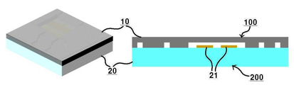
도 1a는 본 발명에서 제안된 단결정 실리콘 마이크로 미러의 전체 사시도이다.1A is an overall perspective view of a single crystal silicon micro mirror proposed in the present invention.
도 1b는 본 발명에서 제안된 단결정 실리콘 마이크로 미러의 단면도이다.1B is a cross-sectional view of the single crystal silicon micro mirror proposed in the present invention.
도 2는 본 발명에서 제안된 마이크로 미러의 미러판에서의 미러판의 크기, 기계적 스프링의 길이 및 폭과의 관계를 나타낸 도면이다.2 is a view showing the relationship between the size of the mirror plate, the length and width of the mechanical spring in the mirror plate of the micromirror proposed in the present invention.
도 3은 마이크로 미러의 라인구동방법을 나타낸 것이다.3 shows a line driving method of the micromirror.
도 4는 마이크로 미러의 프레임구동방법을 나타낸 것이다.4 shows a frame driving method of the micromirror.
도 5는 프레임구동방법에 있어서, 구동전압과 릴리스 전압에 따른 어드레스 전압과 바이어스 전압의 관계를 나타낸 그래프이다.5 is a graph showing a relationship between an address voltage and a bias voltage according to a driving voltage and a release voltage in the frame driving method.
도 6a 내지 도 6d는 본 발명에서 제안된 단결정 실리콘 마이크로 미러의 제작과정을 나타낸 도면이다.6a to 6d are views illustrating a manufacturing process of the single crystal silicon micro mirror proposed in the present invention.
도 7은 단결정 실리콘 마이크로 미러 어레이의 주사형 전자 현미경 사진(a), 측정결과(b) 및 미러판의 가장자리의 주사형 전자 현미경 사진(c)를 나타낸 것이다.Fig. 7 shows a scanning electron micrograph (a) of a single crystal silicon micromirror array, a measurement result (b) and a scanning electron micrograph (c) of the edge of the mirror plate.
도 8은 레이저 프로파일러, SPM 및 3차원 프로파일러를 이용한 마이크로 미러의 미러판 표면의 형상 측정 및 그 결과그래프를 나타낸 것이다.Figure 8 shows the shape measurement and the resulting graph of the surface of the mirror plate of the micro mirror using a laser profiler, SPM and three-dimensional profiler.
도 9는 마이크로 미러 어레이의 구동 전압을 측정하기 위하여 측정 장치의 장치의 개략도와 실제 제작된 장치를 나타낸 것이다.9 shows a schematic diagram of a device of a measuring device and a practically manufactured device for measuring a driving voltage of a micro mirror array.
도 10은 제작된 실리콘 마이크로 미러 어레이의 구동 전압 분포를 나타낸 그래프이다.10 is a graph showing a driving voltage distribution of the fabricated silicon micro mirror array.
도 11은 제작된 마이크로 미러 어레이의 구동 전압의 평균과 평균대비 편차를 나타내는 그래프이다.FIG. 11 is a graph illustrating an average and a deviation from an average of a driving voltage of a manufactured micromirror array. FIG.
도 12a는 마이크로 미러 어레이를 사용하여 펩타이드를 합성할 수 있는 시스템의 개략도이다.12A is a schematic of a system capable of synthesizing peptides using a micro mirror array.
도 12b는 제작된 마이크로 미러 어레이를 이용하여 합성된 펩타이드의 형광 이미지와 그 결과를 측정한 그래프이다.Figure 12b is a graph measuring the fluorescence image and the results of the peptide synthesized using the prepared micro mirror array.
* 도면의 주요 부분에 대한 부호의 설명** Explanation of symbols for the main parts of the drawings *
100 : 제 1기판10 : 단결정 실리콘 기판100: first substrate 10: single crystal silicon substrate
11 : 미러판12 : 기계적 스프링11: mirror plate 12: mechanical spring
13 : 제1 접합부14 : 절연홈13: first junction 14: insulating groove
15 : 제2 접합부15: second joint
200 : 제 2기판20 : 유리기판200: second substrate 20: glass substrate
21 : 바닥전극 21: bottom electrode
본 발명은 펩타이드 합성시에 바이오 어레이 제작에 사용되는 마이크로 미러(또는, 마이크로 미러 어레이)에 관한 것으로서, 보다 상세하게는 단결정 실리콘 기판 및 유리 기판으로 구성하여 비교적 단순한 구조 및 양극 접합을 이용하여 제조방법이 용이하면서도, 광학적으로 평탄한 미러판 및 기계적으로 안정적인 특성을 가질 뿐만 아니라 구동각 및 미러의 크기가 펩타이드 합성에 있어 바이오 어레이 제작에 적합한 단결정 실리콘 마이크로 미러에 대한 것이다.The present invention relates to a micromirror (or micromirror array) used for fabricating a bioarray at the time of peptide synthesis. This easy, optically flat mirror plate and mechanically stable properties, as well as the drive angle and size of the mirror, are for single crystal silicon micromirrors suitable for bioarray fabrication in peptide synthesis.
마이크로 미러는 초소형 또는 미세 거울 소자라고 할 수 있으며, 현재 대형화상 표시장치, 홀로그램을 이용한 정보저장장치 등 광범위하게 응용되고 있다. 상기 대형화상 표시장치에 적용되는 마이크로 미러는 텍사스 인스트루먼트 사에서 개발한 화소 수(100만 - 200만개) 만큼의 16 ㎛ 크기 마이크로 미러를 2차원으로 배열하여 구성한 디지털 마이크로미러 소자(Digital Micromirror Device, DMD)[Peter F. Van Kessel et al. 1998]를 대표적인 예로 들 수 있으며, 상기 DMD는 프로젝터의 핵심부품으로 사용되고 있다. Micro-mirror may be called a miniature or micro-mirror element, and is widely applied to a large image display device and an information storage device using a hologram. The micromirror applied to the large image display device is a digital micromirror device (DMD) formed by arranging 16 micron micromirrors in two dimensions as many as 1 million to 2 million pixels developed by Texas Instruments. Peter F. Van Kessel et al. 1998] is a representative example, and the DMD is used as a core part of a projector.
또한, 차세대 대용량 정보저장 장치로서 각광을 받고 있는 홀로그램을 이용한 정보저장 분야에서도 고속 어드레싱(addressing)을 위한 광원으로서 마이크로머시닝 기술로 제작한 마이크로미러 어레이를 이용하려하고 있다. 상기 마이크로머시닝이란 증착 및 식각 과정을 반복하는 반도체 공정 기술을 이용하여 제조되는 마이크로미터(㎛)급 또는 나노미터(㎚)급의 초소형 3차원 정밀기계를 뜻하며, 전하 간에 발생하는 정전기력(Electrostatic Force) 또는 표면 장력을 전류를 발생시키는 구동력으로 이용하므로, 전력소비량이 작다.In addition, in the field of information storage using holograms, which are in the spotlight as the next generation mass storage device, a micromirror array manufactured by micromachining technology is used as a light source for high-speed addressing. The micromachining refers to a micrometer (μm) or nanometer (nm) class of ultra-small three-dimensional precision machine manufactured using a semiconductor process technology that repeats the deposition and etching process, the electrostatic force generated between the charge (Electrostatic Force) Alternatively, since the surface tension is used as a driving force for generating a current, the power consumption is small.
또한, 마이크로 미러 어레이는 상기 대형화상 표시장치 또는 홀로그램을 응용한 정보저장장치뿐만 아니라 바이오테크놀러지(Bio-Technology: BT)와 정보기술(Information Technology: IT)중 하나인 미세전자기계시스템(Micro-Electro mechanical System: MEMS)이 융합되는 분야에서도 적용되고 있다.In addition, the micro-mirror array is a micro-electromechanical system that is one of biotechnology (BT) and information technology (IT) as well as the information storage device using the large image display device or the hologram. It is also applied in the field of fusion of mechanical systems (MEMS).
즉, DNA, 단백질, 펩타이드(peptide) 등을 한 줄로 또는 2차원적으로 배열한 어레이인 바이오칩을 제작[F. Cerrina et al. 2002]하거나 이들 칩에서 발생하는 형광을 측정하는 시스템에 마이크로미러 어레이가 사용되고 있다. That is, a biochip that is an array in which DNA, proteins, peptides, etc. are arranged in one line or two-dimensionally is manufactured [F. Cerrina et al. 2002] or micromirror arrays are used in systems that measure the fluorescence generated by these chips.
상기와 같이 바이오칩에 응용되는 마이크로 미러는 대형화상 표시장치에 적용되는 마이크로 미러에 대조하여 다음과 같은 특성을 갖는다. As described above, the micromirror applied to the biochip has the following characteristics in contrast to the micromirror applied to the large image display device.
우선, 대형화상 표시장치에 적용되는 마이크로 미러는 화소수만큼의 마이크로 미러를 요구하므로, 하나의 칩에 수십만내지 이백만개의 마이크로 미러를 배열해야하는 반면, 바이오칩에 응용되는 마이크로 미러 어레이는 배열되는 마이크로 미러의 수가 화소수 등에 구애받지 않으며, 수십 내지 수만개의 마이크로 미러를 배열하는 것만으로도 충분한 효과를 발생시킬 수 있는 차이점이 있다.First, since the micromirror applied to the large-scale image display device requires as many micromirrors as the number of pixels, it is necessary to arrange hundreds of thousands to two million micromirrors on one chip, whereas the micromirror array applied to the biochip is the micromirror arranged. The number of pixels is independent of the number of pixels and the like, and there is a difference in that sufficient effect can be generated by arranging tens to tens of thousands of micro mirrors.
또한, 대형화상 표시장치용 마이크로미러 어레이는 미러의 크기가 적어야 좁은 면적에 많은 미러를 제작할 수 있는 반면, 바이오칩 응용의 경우, 미러의 수가 적으므로 미러의 크기가 커져도 소자의 전체 크기가 그리 커지지 않기 때문에 바이오칩에 응용되는 마이크로 미러 어레이는 미러의 크기가 큰 차이점이 있다.In addition, a micromirror array for a large image display device can produce a large number of mirrors in a small area only when the mirror size is small, whereas in the case of biochip applications, the number of mirrors is small, so that the overall size of the device does not become very large even if the mirror size is large. Therefore, the mirror size of the micro mirror array applied to the biochip has a big difference.
또한, 대형화상 표시장치용 마이크로미러 어레이는 미러 간의 간격이 좁아야 화상이 밝고 깨끗하지만, 바이오칩 응용의 경우, 미러 간의 간격이 떨어져 있어야 미러 간의 간섭을 줄일 수 있기 때문에 바이오칩에 응용되는 마이크로 미러 어레이는 미러 간에 소정 간격으로 이격되어 배열되는 것이 바람직하다. In addition, micromirror arrays for large image display devices have bright and clean images when the mirrors have a narrow gap, but in the case of biochip applications, micromirror arrays applied to biochips can be reduced because the distance between mirrors can be reduced to reduce the interference between mirrors. It is preferable that the mirrors are arranged at a predetermined interval apart from each other.
또한, 대형화상 표시장치용 마이크로미러 어레이는 각각의 마이크로 미러가 하나의 화소를 구성하므로 100만개의 마이크로미러 중 5개 이하로 결손이 되어야 양품 판정을 받을 수 있다. 그러나, 바이오칩 응용의 경우, 이보다는 훨씬 낮은 정도의 사양으로도 적용이 가능하므로, 바이오칩에 응용되는 마이크로 미러 어레이는 마이크로 미러 간의 오차 또는 신뢰성의 요구 정도가 대형화상 표시장치에 적용되는 마이크로미러의 경우보다 낮다.In addition, since each micromirror constitutes one pixel, a micromirror array for a large-scale display device may have a defect of less than 5 out of 1 million micromirrors in order to receive a good product judgment. However, in the case of biochip applications, even a much lower specification can be applied. Therefore, in the case of a micromirror applied to a biochip, a micromirror in which an error or reliability requirement between micromirrors is applied to a large image display device is required. Lower than
상기 대형화상 표시 장치에 적용되는 마이크로 미러 어레이는 텍사스인스트루먼트 사가 독보적으로 연구하고 있다. 그러나, 홀로그램 또는 바이오칩에 적용되는 마이크로 미러 어레이는 해외에 대형화상 표시장치용 마이크로 미러 어레이를 이용하는 연구팀이 있을 뿐이며, 앞서 언급한 바와 같이, 상기 대형화상 표시장치용 마이크로 미러 어레이는 바이오칩에 적용되기에 적합하지 않다.Texas Instruments, Inc. has been exclusively studying micro mirror arrays applied to the large image display devices. However, a micro mirror array applied to a hologram or a biochip has a research team using a micro mirror array for a large image display device overseas, and as mentioned above, the micro mirror array for a large image display device is applied to a biochip. Inappropriate.
상기와 같이, 마이크로 미러는 응용되는 분야에 따라서 그 사양과 성능이 달라져야하며, 따라서, 적용될 분야에 따라 마이크로 미러의 설계, 제작 방법 및 측정 방법을 다르게 결정지어야 할 것이다. 이에, 바이오칩에 적용되는 마이크로 미러 어레이의 설계 및 제조방법에 대한 연구가 계속되고 있다.As described above, the specification and performance of the micromirror should vary according to the application field, and therefore, the design, fabrication method, and measurement method of the micromirror should be determined differently according to the application field. Accordingly, research on the design and manufacturing method of a micro mirror array applied to a biochip continues.
현재까지 상기 바이오칩에 적용되는 대다수의 마이크로 어레이는 알루미늄으로 제작되어 왔다. 마이크로 어레이를 알루미늄으로 제작할 경우에는 CMOS(Complementary Metal-Oxide Semiconductor)회로와의 집적화가 가능할 뿐만 아니라 50 ㎛ 이하의 작은 크기로 제조되는 것도 가능하다. 또한, 높은 반사율을 가지므로, 편평하게 제작될 경우 높은 광학 효율을 가질 수 있다. 그러나, 알루미늄으로 제작된 마이크로 미러는 다음과 같은 단점이 있다.To date, most microarrays applied to the biochip have been made of aluminum. When the microarray is made of aluminum, it can be integrated with a complementary metal-oxide semiconductor (CMOS) circuit and can be manufactured with a small size of 50 μm or less. In addition, since it has a high reflectance, it can have high optical efficiency when it is manufactured flat. However, the micro mirror made of aluminum has the following disadvantages.
우선, 마이크로 미러의 크기가 커지면 알루미늄의 잔류응력과 공정상의 한계로 인하여 미러판의 변형이 발생하는 단점이 있다. 상기 미러판의 변형은 광학 효율을 감소시키고 마이크로미러 어레이를 사용하는 시스템의 성능을 저하시키게 된다. 또한, 알루미늄으로 제작되는 기계적 스프링은 그 길이가 증가하게 되면, 변형이 발생할 수 있으므로, 이에 따라 각각의 마이크로 미러마다 구동전압 또는 구동각이 같지 않게 되는 단점이 발생된다. 또한 알루미늄과 같은 금속의 경우에는 파괴응력에 도달하기 전에, 피로 현상이 발생할 수 있다. 상기 피로 현상에 의해, 마이크로 미러를 반복하여 장시간 구동할 경우 원래의 위치로 돌아오지 못하게 되어, 초기구동각의 변화가 발생할 수 있다. First, when the size of the micromirror increases, deformation of the mirror plate occurs due to the residual stress of aluminum and process limitations. Deformation of the mirror plate reduces optical efficiency and degrades the performance of a system using a micromirror array. In addition, mechanical springs made of aluminum may be deformed when its length is increased, thereby causing disadvantages in that driving voltages or driving angles are not the same for each micromirror. In addition, in the case of metals such as aluminum, fatigue may occur before the fracture stress is reached. Due to the fatigue phenomenon, when the micromirror is repeatedly driven for a long time, the micromirror may not return to the original position, and a change in the initial driving angle may occur.
따라서, 기존에 주로 연구되던 알루미늄 등으로 제작된 마이크로미러는 구동각의 불균일, 구동전압의 불균일, 비교적 짧은 수명으로 인해 실제적으로 응용에 어려움이 있었다.Therefore, the micromirror made of aluminum, which has been mainly studied in the past, has practical difficulties in application due to uneven driving angle, uneven driving voltage, and relatively short lifespan.
본 발명은 종래 기술의 문제점을 해결하기 위한 것으로서, 단결정 실리콘과 절연기판이 접합된 구조로 구성됨으로서, 광학적으로 미러판이 보다 편평하고, 기계적 스프링의 변형이 적으며, 어레이에 배열되는 각각의 마이크로 미러의 성능이 균일할 뿐만 아니라 비교적 긴 수명을 가짐에 따라 펩타이드 합성 시에 바이오 패턴 어레이 제작에 적용되기에 적합한 마이크로 미러를 제안하는 데에 그 목적이 있다.SUMMARY OF THE INVENTION The present invention has been made to solve the problems of the prior art, and is composed of a structure in which a single crystal silicon and an insulating substrate are bonded to each other, so that the mirror plate is optically flatter, the deformation of the mechanical spring is small, and each micromirror arranged in the array. The purpose of the present invention is to propose a micromirror suitable for application to biopattern array fabrication during peptide synthesis due to its uniform performance and relatively long lifetime.
또한, 상기 단결정 실리콘과 유리기판을 접합함으로서, 바닥전극과 미러판의 전압차이로 인한 정전력을 이용하여 미러판이 작은 구동각으로 회전할 수 있는 마이크로 미러를 제안하는 데에 그 목적이 있다.Another object of the present invention is to propose a micromirror capable of rotating a mirror plate at a small driving angle by using a constant power due to a voltage difference between a bottom electrode and a mirror plate by bonding the single crystal silicon and a glass substrate.
본 발명은 상기 목적을 달성하기 위하여, 펩타이드 합성의 바이오 패턴 어레이 제작에 사용되는 마이크로 미러에 있어서, 전압이 인가되도록 구성한 제1 전극패드 및 제2 전극패드와 각각 전기적으로 연결되는 제1 접합부 및 제2 접합부, 상기 제1 접합부와 기계적 스프링을 통해 전기적으로 연결되며 상기 기계적 스프링을 중심축으로 하여 회전하는 미러판을 포함하며, 단결정 실리콘으로 구성되는 제1 기판; 및 상기 미러판과 전기적으로 분리되고, 상기 미러판의 하부에 일정 거리 이격되어 위치하며, 상기 제2 접합부와 전기적으로 연결되고 금속으로 구성된 바닥전극을 포함하며, 절연체로 구성된 제2 기판; 을 포함하는 단결정 실리콘 마이크로 미러를 제안한다.In order to achieve the above object, the present invention provides a micro-mirror used for fabricating a biopattern array for peptide synthesis, wherein the first junction and the second electrode pad are electrically connected to each of the first and second electrode pads configured to apply voltage. A second substrate, the first substrate being electrically connected to the first junction through a mechanical spring and including a mirror plate rotating around the mechanical spring, the first substrate being made of single crystal silicon; And a second substrate electrically separated from the mirror plate and positioned below the mirror plate at a predetermined distance, and including a bottom electrode electrically connected to the second junction and made of a metal; We propose a single crystal silicon micro mirror comprising a.
상기 기계적 스프링 및 미러판은 상기 제1 기판에 적어도 하나 이상 구성되고, 상기 제 2 기판의 바닥 전극은 상기 미러판이 구성된 것과 같이 상기 제2 기판에 적어도 하나 이상 구성되는 것이 바람직하며, 상기 기계적 스프링, 미러판 및 바닥전극은 2차원으로 배열되는 것이 더욱 바람직하다. 또한, 상기 2차원으로 배열되는 미러판은 프레임구동방법(frame driving scheme)으로 구동되는 것이 더욱 바람직하다.Preferably, at least one mechanical spring and a mirror plate are configured on the first substrate, and at least one bottom electrode of the second substrate is configured on the second substrate as the mirror plate is configured. More preferably, the mirror plate and the bottom electrode are arranged in two dimensions. Further, the mirror plates arranged in two dimensions are more preferably driven by a frame driving scheme.
상기 미러판은 기계적 스프링을 회전축으로 하여 제1 전극패드 및 제2 전극패드에 인가된 전압에 비례하여 일정 각도로 회전하는 것이 바람직하다. 또한, 상기 제1 전극패드 및 제2 전극패드는 단결정 실리콘으로 구성되는 것이 바람직하다. The mirror plate may be rotated at a predetermined angle in proportion to the voltage applied to the first electrode pad and the second electrode pad by using a mechanical spring as a rotation axis. In addition, the first electrode pad and the second electrode pad are preferably composed of single crystal silicon.
상기 제2 기판을 구성하는 절연체는 유리인 것이 바람직하다.It is preferable that the insulator which comprises the said 2nd board | substrate is glass.
상기 제 1접합부 및 제2 접합부는 제2 기판이 노출되도록 형성된 절연홈에 의해 전기적으로 분리되는 것이 바람직하다.Preferably, the first junction and the second junction are electrically separated by an insulating groove formed to expose the second substrate.
또한, 본 발명은, a. 제1 실리콘 층, 산화막, 제2 실리콘층으로 구성되는 다중층의 단결정 실리콘 기판에 미러판 및 절연홈이 구성될 부분에 공동(cavity)을 형성하여 제1 기판을 마련하는 단계; b. 절연 기판에 바닥 전극을 구성하여 제2 기판을 마련하는 단계; c. 상기 제1 기판의 공동이 형성된 부분과 제2 기판의 바닥 전극을 구성한 부분이 서로 마주보도록 위치시킨 후, 상기 제1 기판 및 제2 기판을 접합하는 단계; d. 상기 제1 기판의 두께를 조절하기 위하여 상기 제1 기판을 식각하는 단계; 및 e. 상기 제1 기판에 미러판, 기계적 스프링 및 절연홈을 형성 하는 단계; 를 포함하는 단결정 실리콘 마이크로 미러의 제조방법을 제안한다.In addition, the present invention, a. Providing a first substrate by forming a cavity in a portion where a mirror plate and an insulating groove are to be formed in a multilayer single crystal silicon substrate including a first silicon layer, an oxide film, and a second silicon layer; b. Forming a bottom electrode on the insulating substrate to prepare a second substrate; c. Joining the first substrate and the second substrate after positioning the cavity of the first substrate and the part of the bottom electrode of the second substrate to face each other; d. Etching the first substrate to adjust the thickness of the first substrate; And e. Forming a mirror plate, a mechanical spring, and an insulating groove in the first substrate; We propose a method of manufacturing a single crystal silicon micro mirror comprising a.
상기 c단계는 상기 제2 기판의 바닥 전극과 상기 제1 기판이 접촉하도록 위치시킨 후, 양극 접합(anodic bonding)을 통해 수행되는 것이 바람직하며, 상기 a단계 내지 d단계는 다수 개의 마이크로 미러 어레이를 형성하는 웨이퍼의 형태로 수행되며, 상기 d단계를 수행한 후, 개개의 마이크로 미러 어레이로 분리하기 위한 홈을 형성하는 다이싱단계 및 개개의 마이크로 미러 어레이로 분리하기 위하여 홈부분을 제거하는 건식식각단계를 추가적으로 포함하는 것이 바람직하다. 또한, 본 발명은 상기 단결정 실리콘 마이크로 미러의 제조방법으로 제조되어 펩타이드 합성시에 바이오 패턴 어레이의 제작에 사용되는 것을 특징으로 하는 단결정 실리콘 마이크로 미러를 제안한다.The step c is preferably performed by anodic bonding after positioning the bottom electrode of the second substrate and the first substrate to be in contact with each other, and the steps a to d comprise a plurality of micro mirror arrays. It is performed in the form of a wafer to be formed, and after performing the d step, a dicing step for forming a groove for separating into individual micro mirror arrays and dry etching for removing grooves for separation into individual micro mirror arrays. It is preferred to further include the step. In addition, the present invention proposes a single crystal silicon micro mirror, which is manufactured by the method of manufacturing the single crystal silicon micro mirror and used for fabrication of a bio pattern array during peptide synthesis.
이하에는 첨부된 도면을 참고하여, 본 발명의 바람직한 실시예에 대하여 보다 상세히 설명한다.Hereinafter, with reference to the accompanying drawings, it will be described in detail a preferred embodiment of the present invention.
마이크로 미러는 미세구동기 중 하나로서, 상기 미세구동기는 마이크로머시닝 기술을 이용한 구동기이다. 상기 마이크로머신이란 증착과 식각을 반복하여 수행하는 반도체 공정기술을 이용하여 제조되는 초소형 3차원 정밀기계를 뜻한다. 상기 마이크로머신은 전하 간에 발생하는 힘인 정전기력과 표면 장력을 전류를 발생시키는 구동력으로 사용함으로서, 전력소비량이 작은 특징이 있다. 상기 마이크로머시닝은 나노 및 시스템 온 칩(SoC)에 응용되고 있다. 상기 미세구동기는 광반사용 초소형 미러어레이, 초소형 액추에이터, 초소형 구조물, 초소형 센서 및 초소형 구동기 등으로 구분될 수 있다.The micro mirror is one of the micro drivers, and the micro drivers are drivers using micromachining technology. The micromachine refers to an ultra-small three-dimensional precision machine manufactured by using a semiconductor process technology that repeatedly performs deposition and etching. The micromachine uses the electrostatic force, which is a force generated between charges, and surface tension as a driving force for generating a current, and thus has a small power consumption. The micromachining is applied to nano and system on chip (SoC). The micro driver may be classified into a light reflecting micro mirror array, a micro actuator, a micro structure, a micro sensor, and a micro driver.
본 발명에서는 펩타이드 합성에 적용될 수 있는 광반사용 마이크로 미러 어레이를 제안한다.The present invention proposes a light reflecting micro mirror array that can be applied to peptide synthesis.
종래의 마이크로 미러 어레이는 주로 금속이나 다결정 실리콘을 그 구조재로 이용하였고, 희생층 공정을 통하여 제작되어왔다. 그러나 금속 또는 다결정 실리콘으로 구성되는 마이크로 미러 어레이는 상기 금속 또는 다결정 실리콘이 고유적으로 갖는 특성때문에, 제조시에 인가하는 열에 의해 변형될 수 있고, 이에 따라 마이크로 미러의 효율적인 특성을 기대하기 힘들다. 또한 이러한 변형은 한 기판 내에서 불균일하게 발생하기 때문에, 한 기판에서 생성되는 마이크로 미러 간의 특성 분포가 고르지 못하게 되어 제품의 안정성에 문제가 발생될 수 있다.Conventional micromirror arrays mainly use metal or polycrystalline silicon as their structural material, and have been manufactured through sacrificial layer processes. However, micromirror arrays composed of metal or polycrystalline silicon may be deformed by heat applied at the time of manufacture due to the inherent properties of the metal or polycrystalline silicon, and thus it is difficult to expect the efficient properties of the micromirror. In addition, since such deformation occurs non-uniformly in one substrate, uneven distribution of characteristics between micromirrors generated in one substrate may cause problems in product stability.
또한, 마이크로 미러 어레이가 복잡한 구조를 갖도록 설계되면, 복잡한 제조공정이 요구되고, 이에 따라 소자의 신뢰성이 작아지는 문제점이 발생될 수 있다. 이에, 본 발명에서 제안하는 마이크로 어레이는 용이한 제조공정을 위해 비교적 간단한 구조를 갖도록 설계되었다.In addition, when the micro mirror array is designed to have a complicated structure, a complicated manufacturing process is required, and thus, a problem that the reliability of the device may be reduced may occur. Therefore, the micro array proposed in the present invention is designed to have a relatively simple structure for easy manufacturing process.
도 1a는 본 발명에서 제안된 단결정 실리콘 마이크로 미러의 전체 사시도이다. 도 1b는 본 발명에서 제안된 단결정 실리콘 마이크로 미러의 단면도이다.1A is an overall perspective view of a single crystal silicon micro mirror proposed in the present invention. 1B is a cross-sectional view of the single crystal silicon micro mirror proposed in the present invention.
도 1a 내지 도 1b에 도시한 바와 같이, 본 발명에서는 종래의 금속 또는 다결정 실리콘으로 구성되는 마이크로 미러 어레이의 문제점을 해결하기 위하여, 미러판(11), 기계적 스프링(12)등을 구성한 단결정 실리콘 기판(10, 제1 기판(100))과, 바닥전극(21)을 구성한 절연기판(20, 제2 기판(200))을 별도로 준비한 후, 상기 두 기판을 접합함으로서 마이크로 미러 어레이를 구성하는 것을 특징으로 한다. 상기 제1 기판(100)은 일체의 단결정 실리콘으로 구성된 미러판(11), 기계적 스프링(12, 또는, 스프링), 접합부 및 절연홈(14)을 포함하며, 상기 제2 기판(200)은 상기 미러판(11) 하부에 소정 간격으로 이격되어 위치하는 바닥전극(21)을 포함하는 절연기판으로 구성된다.As shown in Figs. 1A to 1B, in the present invention, in order to solve the problem of a conventional micro mirror array composed of a metal or polycrystalline silicon, a single crystal silicon substrate including a
상기 미러판(11)은 마이크로 미러 어레이에 전압을 인가하는 제1 전압패드와 전기적으로 연결된 제1 접합부(13)와 기계적 스프링(12)을 통해 연결된다. 상기 미러판(11)은 두 개의 기계적 스프링(12)과 전기적으로 연결되는데, 상기 두 개의 기계적 스프링(12)은 서로 마주보도록 위치하는 것이 바람직하다. 상기 미러판(11)에는 상기 제1 전극패드에 인가된 전압이 공급되며, 상기 미러판(11)이 구동되도록 하기 위하여, 상기 미러판(11)의 하부에 위치하는 제2 기판(200)의 바닥 전극에는 마이크로 미러 어레이에 전압을 인가하는 제2 전압패드와 전기적으로 연결된 제2 접합부(15)와 연결된다. 상기 제2 접합부(15)와 바닥전극(21)은 상기 제1 기판(100)과 제2 기판(200)을 접합함으로 인해 전기적으로 연결되는 것이 바람직하다.The
상기 미러판(11), 기계적 스프링(12), 제1 접합부(13), 제2 접합부(15) 및 절연홈(14)은 일체의 단결정 실리콘으로 구성되고, 상기 제1 접합부(13)와 제2 접합부(15)에 서로 다른 전압이 인가되므로, 상기 제1 접합부(13)와 제2 접합부(15)가 서로 절연되도록 하기 위한 절연홈(14)이 형성된다. 상기 절연홈(14)은 상기 제1 접합부(13)와 제2 기판(200)의 바닥전극(21)이 서로 연결되지 않도록 하고, 상기 미러판(11)과 제2 접합부(15)가 전기적으로 연결되지 않도록 구성된다. The
또한, 상기 미러판(11)은 광을 반사하는 부분이 되므로, 미러판(11)의 광반사율을 확보하기 위해서, 상기 외부와 접촉하는 미러판(11)의 표면에는 얇은 금속층이 증착되어 형성되는 것이 바람직하다.In addition, since the
상기 제1 기판(100)과 제2 기판(200)은 양극 접합(anodic bonding)을 이용하여 접합하는 것이 바람직하므로, 상기 절연기판으로 구성되는 상기 제2 기판(200)은 유리 기판(Pyrex 7740)을 사용하는 것이 바람직하다. 이는 유리 기판이 4.82의 비유전율을 가지며, 석영기판에 비해 비교적 유전체 손실이 크지만 양극 접합을 통해서 밀봉 접합이 가능하기 때문이다. 상기 양극 접합이란, 실리콘기판과 열팽창계수가 비슷한 파이렉스(Pyrex) 유리를 접합시키는 기술이다. 보다 상세하게는 상기 파이렉스 유리에는 나트륨(Na), 칼륨(K)등의 불순물이 일정량 함유되어 있어, 상기 파이렉스 유리에 소정 온도(예를 들어 200 ℃) 이상으로 가열하면 상기 불순물이 전하를 띄게되어 전압에 따라 쉽게 이동하게 된다. 상기 실리콘 기판(10)과 파이렉스 유리 기판(20)을 서로 접촉하도록 정렬시킨 후, 양쪽에 소정 전압(예를 들어 600 V)이상의 직류전압을 인가하면, 상기 파이렉스 유리 기판(20)에 형성되는 이동성 전하는 급속히 이동하게 되며, 상기 이동성 전하에 의해 실리콘 기판(10)과 유리 기판(20)의 계면에는 강한 대전현상이 발생되어 상기 실리콘 기판(10)과 유리기판이 접합한다.Since the
또한, 상기 마이크로 미러는 상기 미러판(11)과 전기적으로 연결된 마이크로 미러 어레이의 제1 전극패드와 제2 기판(200)의 바닥 전극과 전기적으로 연결된 제2 전극패드에 전압을 인가할 때, 상기 미러판(11)과 바닥 전극 사이에서 발생되는 정전력에 의해 상기 미러판(11)이 기계적 스프링(12)을 축으로 하여 회전된다. 이때 상기 기계적 스프링(12)과 연결되어 있는 미러판(11)이 회전되는 각도에 따라 반사되는 빛의 방향이 결정되며 이러한 과정을 통해 상기 마이크로 미러에 의해 광반사가 발생된다. In addition, the micromirror when the voltage is applied to the first electrode pad of the micromirror array electrically connected to the
또한 본 발명에서 제안하는 마이크로 미러는 미러판(11)과 각각 연결되며 서로 마주보도록 위치한 두 개의 기계적 스프링(12)을 포함하며, 상기 기계적 스프링(12)은 상기 미러판(11)의 두께와 동일한 두께를 갖도록 구성하였다. 또한, 미러판(11)의 반사면의 면적은 감소하지만, 마이크로미러 어레이에 배열되는 각각의 마이크로 미러 사이의 간격을 조절할 수 있도록 기계적 스프링(12)을 미러판(11) 안쪽에 위치하도록 구성하였다. In addition, the micro-mirror proposed in the present invention includes two
도 1b에 도시한 바와 같이, 상기 미러판(11)의 하부에는 소정 거리 이격되어 위치하는 두 개의 바닥 전극이 상기 기계적 스프링(12)을 중심축으로 하여 양쪽에 위치하므로, 상기 각각의 바닥 전극과 미러판(11)에 인가되는 전압에 따라, 상기 미러판(11)은 상기 기계적 스프링(12)을 회전축으로 하여, 오른쪽 또는 왼쪽을 바라보도록 회전된다. As shown in FIG. 1B, two bottom electrodes positioned below the
또한 상기 마이크로미러 어레이에 형성되는 제1 전극패드 및 제2 전극패드도 단결정 실리콘으로 구성되므로, 상기 전극패드간의 절연을 위하여 절연홈(14)을 형성하였다. In addition, since the first electrode pad and the second electrode pad formed in the micromirror array are also made of single crystal silicon, an insulating
또한 앞서 언급한 바와 같이, 상기 제2 전극에 위치하는 바닥 전극은 단결정 실리콘으로 구성되는 제1 기판(100)의 제2 접합부(15)와 전기적으로 연결되어, 상기 제2 접합부(15)와 전기적으로 연결된 제2 전극패드에 인가된 전압이 인가받을 수 있다. 상기 바닥전극(21)과 제2 접합부(15)는 상기 제1 전극과 제2 전극을 양극접합을 통해 접합함과 동시에 서로 연결된다.In addition, as mentioned above, the bottom electrode positioned on the second electrode is electrically connected to the
도 2는 본 발명에서 제안된 마이크로 미러의 미러판(11)에서의 미러판(11)의 크기, 기계적 스프링(12)의 길이 및 폭과의 관계를 나타낸 도면이다.2 is a view showing the relationship between the size of the
상기 마이크로 미러에 있어서, 미러판(11)이 회전되기 위한 구동 전압은 미러판(11)의 크기 및 두께와, 스프링의 폭, 길이 및 두께와 바닥 전극의 크기, 바닥 전극과 미러판(11) 사이의 간격 등의 여러가지 요소를 복합적으로 해석하여 결정될 수 있다. In the micromirror, the driving voltage for rotating the
이에 미러판(11)의 크기와 스프링의 형상을 결정하기 위하여 수식을 통한 해석을 수행하였다. 다음 수학식 1은 제안된 마이크로 미러 어레이의 전기적 회전력에 관한 식을 보여준다. 수학식 1에 나타난 각각의 변수는 도 2에 도시한 바와 같다.In order to determine the size of the
기본적으로, 미러판(11)의 공진 주파수는 10 kHz, 실리콘 기판(제1 기판(100))의 두께는 6 ㎛, 구동전압은 100 V로 고정시킨 후, 상기 미러판(11)의 크기와 기계적 스프링(12)의 폭 및 길이를 결정하는 과정을 수행하였다. Basically, the resonance frequency of the
도 2에 도시한 것과 같이, 미러판(11)은 상기 미러판(11)에 인가되는 전압(제1 전극패드에 인가되는 전압)과 제2 기판(200)의 바닥전극(21)에 인가되는 전압(제2 전극패드에 인가되는 전압)에 의해 정전력이 발생되며, 상기 정전력에 의해 상기 미러판(11)은 기계적 스프링(12)을 회전축으로 하여 회전하게 된다.As shown in FIG. 2, the
도 2와 같은 구조를 갖는 미러판(11)은, 수학식 1에 나타낸 바와 같이, 상기 기계적 스프링(12)의 폭(Spring width(㎛))이 좁을수록 또한 기계적 스프링(12)의 길이(Spring length(㎛))가 길수록, 스프링 상수가 작아지므로 공진 주파수는 떨어지게 된다. 따라서, 미러판(11)의 크기가 커져서 미러판(11) 전체의 질량이 증가하게 되면, 기계적 스프링(12)의 폭이 커지거나 또는 길이가 짧도록 설계하여 상기 스프링 상수를 증가시킴으로 인해 일정한 공진 주파수를 얻게 된다. As shown in
앞서 언급한 바와 같이, 본 발명에서 제안하는 단결정 실리콘 마이크로 미러는 단결정 실리콘으로 기계적으로 구동되는 모든 부분을 구성함으로서, 광반사면의 거칠기가 우수하게 된다. 또한, 비교적 안정한 상태인 단결정 실리콘을 이용하므로 열이나 외부 응력에 의한 변형이 발생되지 않는 장점이 있다. 이에 따라, 단결정 실리콘으로 구성되는 마이크로 미러 어레이 소자는 하나의 기판에서 제조되는 다수 개의 마이크로 미러 어레이가 전기적 및 기계적인 특성이 균일하며, 이에 소자의 안정성 및 신뢰성을 향상시킬 수 있다.As mentioned above, the monocrystalline silicon micromirror proposed in the present invention constitutes all parts mechanically driven by single crystal silicon, so that the roughness of the light reflection surface becomes excellent. In addition, since the single crystal silicon in a relatively stable state is used, there is an advantage that deformation by heat or external stress does not occur. Accordingly, in the micromirror array device composed of single crystal silicon, a plurality of micromirror arrays manufactured from one substrate have uniform electrical and mechanical characteristics, thereby improving stability and reliability of the device.
상기 마이크로미러는 제2 기판의 바닥전극에 인가하는 어드레스 전압과 미러판에 인가하는 바이어스 전압에 의해 전압차가 발생하고, 상기 전압차에 의해 상기 미러판이 회전하면서 구동된다. 상기 어드레스 전압은 상기 바닥기판과 전기적으로 연결된 제2 접합부에 전기적으로 연결된 제2 전극패드에 인가되며, 상기 바이어스 전압은 상기 미러판과 기계적 스프링을 통해 연결된 제1 접합부에 전기적으로 연결된 제1 전극패드에 인가된다. The micromirror generates a voltage difference due to an address voltage applied to the bottom electrode of the second substrate and a bias voltage applied to the mirror plate, and is driven while the mirror plate is rotated by the voltage difference. The address voltage is applied to a second electrode pad electrically connected to a second junction electrically connected to the bottom substrate, and the bias voltage is first electrode pad electrically connected to a first junction connected to the mirror plate via a mechanical spring. Is applied to.
상기 마이크로미러의 구동방법에는 라인구동방법(line driving scheme)과 프레임구동방법(frame driving scheme)이 있다. 도 3은 마이크로 미러의 라인구동방법을 나타낸 것이며, 도 4는 마이크로 미러의 프레임구동방법을 나타낸 것이다. 도 5는 프레임구동방법에 있어서, 구동전압과 릴리스 전압에 따른 어드레스 전압과 바이어스 전압의 관계를 나타낸 그래프이다.The micromirror driving method includes a line driving scheme and a frame driving scheme. 3 illustrates a line driving method of the micromirror, and FIG. 4 illustrates a frame driving method of the micromirror. 5 is a graph showing a relationship between an address voltage and a bias voltage according to a driving voltage and a release voltage in the frame driving method.
도 3에서는 왼쪽으로부터 1열, 2열, 3열과, 위쪽으로부터 1행, 2행, 3행으로 배열된 9개의 미러판을 갖는 마이크로 미러 어레이가 라인구동방법으로 구동되는 것을 나타내었다. 도 3(a)는 단 하나의 미러판도 구동되지 않는 초기상태를 도시한 것이다. 도 3(b)는 1열에 위치한 미러판들 중 구동될 미러판이 위치한 행에 어드레스 전압을 인가한 것을 도시한 것이다. 도 3(b)에서는 1행과 3행에 어드레스 전압이 인가된 것으로 도시되었다. 이후, 도 3(c)에 도시한 것처럼, 구동할 열(1열)에 바이어스 전압을 인가한다. 이로서, 도 3(c)에 도시한 바와 같이, 상기 어드레스 전압과 바이어스 전압이 모두 인가되는 미러판은 어드레스 전압이 인가된 바닥 전극에 따라 결정된 방향으로 회전된다. 즉, 상기 어드레스 전압과 바이어스 전압이 교차하는 1열1행과 1열3행의 미러판이 구동된다. 또한, 상기 어드레스 전압은 좌우에 위치하는 것으로 도시한 바닥전극 중 좌측 바닥전극에 인가되어, 상기 1열1행과 1열3행의 미러판은 모두 좌측을 바라보도록 회전하였다. 이후, 어드레스 전압과 바이어스 전압을 제거하고, 미러 어레이를 초기상태로 되돌린다.(도 3(d)) 이후, 도 3(e)에 도시한 바와 같이, 2열에 위치한 미러판을 구동하기 위하여, 상기 2열에 위치한 미러판 중 구동될 미러판이 위치한 행에 어드레스 전압을 인가한다. 도 3(e)에서는 2행 및 3행에 위치한 미러판의 좌측 바닥전극에 어드레스 전압이 인가된 것으로 도시하였다. 이후, 도 3(f)에 도시한 바와 같이, 2열에 바이어스 전압을 인가함으로서, 2열2행 및 2열3행의 미러판이 좌측방향을 바라보도록 회전한다. 3 shows that the micromirror array having nine mirror plates arranged in one row, two rows and three rows from the left and one row, two rows and three rows from the top is driven by the line driving method. 3 (a) shows an initial state in which no mirror plate is driven. FIG. 3 (b) shows that an address voltage is applied to a row where a mirror plate to be driven is located among mirror plates located in one column. In FIG. 3B, the address voltages are applied to the first and third rows. Thereafter, as shown in Fig. 3C, a bias voltage is applied to the column (column 1) to be driven. Thus, as shown in Fig. 3C, the mirror plate to which both the address voltage and the bias voltage are applied is rotated in the direction determined according to the bottom electrode to which the address voltage is applied. That is, the mirror plates of one column, one row and one column and three rows in which the address voltage and the bias voltage cross each other are driven. In addition, the address voltage is applied to the left bottom electrode among the bottom electrodes shown to be located at the left and right, so that the mirror plates of one column, one row, and one column, three rows are rotated to face the left side. Thereafter, the address voltage and the bias voltage are removed, and the mirror array is returned to its initial state (Fig. 3 (d)). As shown in Fig. 3 (e), in order to drive the mirror plates located in two columns, An address voltage is applied to a row where a mirror plate to be driven is located among the mirror plates located in the second column. In FIG. 3E, the address voltage is applied to the left bottom electrode of the mirror plates positioned in the 2nd and 3rd rows. Thereafter, as shown in FIG. 3 (f), by applying a bias voltage to two columns, the mirror plates of two rows, two rows, and two columns and three rows rotate to face the left direction.
상기와 같이 구동되는 라인구동방법은 하나의 열로만 구동되므로, 상기 어드레스 전압과 바이어스 전압이 교차함으로서 발생하는 전압차만 고려하면 된다. 그러나 상기 라인구동방법으로 마이크로 미러 어레이를 구동하게 되면, 상기 열단위로 패턴을 맞추어 자외선을 조사하고, 이후 초기상태로 만든 뒤 다음 열단위로 패턴을 맞추어 자외선을 조사하는 과정을 반복하여야 한다. 이에 따라 16개의 열로 배열된 미러판으로 구성되고, 라인구동방법으로 구동되는 미러 어레이를 펩타이드 합성에 적용할 경우에는 16번의 패턴형성 및 16번의 자외선 조사과정이 필요하게 되므로, 시간 낭비 및 자외선의 낭비가 불가피한 단점이 있다.Since the line driving method driven as described above is driven by only one column, only the voltage difference generated by the intersection of the address voltage and the bias voltage needs to be considered. However, when the micromirror array is driven by the line driving method, ultraviolet rays are irradiated by adjusting the pattern by the heat unit, and then, the process is performed after making the initial state and irradiating the ultraviolet rays by adjusting the pattern by the next column unit. Accordingly, when applying the mirror array driven by the line driving method to the peptide synthesis, 16 patterns are formed and 16 UV irradiation processes are required, which is a waste of time and ultraviolet rays. There is an inevitable disadvantage.
도 4에서는 왼쪽으로부터 1열, 2열, 3열과, 위쪽으로부터 1행, 2행, 3행으로 배열된 9개의 미러판을 갖는 마이크로 미러 어레이가 프레임구동방법으로 구동되는 것을 나타내었다. 도 4(a)는 단 하나의 미러판도 구동되지 않는 초기상태를 도시한 것이다. 도 4(b)는 1열에 위치한 미러판들 중 구동될 미러판이 위치한 행에 어드레스 전압을 인가한 것을 도시한 것이다. 도 4(b)에서는 1행과 3행에 위치한 미러판은 좌측 바닥전극에 어드레스 전압이 인가되고, 2행에 위치한 미러판은 우측 바닥전극에 어드레스 전압이 인가된 것으로 도시되었다. 이때, 상기 어드레스 전압은 바닥전극에 전하가 축적되는 것을 방지하기 위하여, 작은 값을 갖는 것이 바람직하며, 이에 따라, 프레임구동방법에 있어서, 상기 어드레스 전압은 미러판이 구동되도록 하는 구동전압을 형성하는 데보다, 상기 미러판이 회전되는 방향을 결정짓는 데에 의미가 있다.4 shows that the micromirror array having nine mirror plates arranged in one row, two rows and three columns from the left and one row, two rows and three rows from the top is driven by the frame driving method. 4 (a) shows an initial state in which no mirror plate is driven. 4 (b) shows that an address voltage is applied to a row where a mirror plate to be driven is located among mirror plates located in one column. In FIG. 4B, the mirror plates positioned in
이후, 도 4(c)에 도시한 것처럼, 구동할 열(1열)에 바이어스 전압을 인가하여, 어드레스 전압이 인가된 바닥전극의 방향에 따라 결정되는 방향으로 미러판이 회동된다. 즉, 좌측 바닥전극에 어드레스 전압이 인가된 1열1행과 1열3행의 미러판은 좌측으로 회전하며, 우측 바닥전극에 어드레스 전압이 인가된 1열2행의 미러판은 우측으로 회전한다. 이후 상기 어드레스 전압은 모두 제거한다.(도 4(d)) 또한, 상기 1열에는 바이어스 전압대신 릴리스전압(release voltage)를 인가한다.Thereafter, as shown in FIG. 4C, the bias plate is applied to the column (column 1) to be driven, and the mirror plate is rotated in a direction determined according to the direction of the bottom electrode to which the address voltage is applied. That is, the mirror plates of 1
앞서 언급한 바와 같이, 상기 어드레스 전압은 전하가 축적될 것을 방지하기 위하여 작은 값을 가지므로 바닥전극과 미러판 사이의 전압차에 크게 고려되지 않는다. 또한, 상기 1열에 위치하는 미러판은 이미 구동되어 바닥 전극과의 거리가 가까우므로, 미러판이 회전된 상태 그대로 유지하는 것은 상기 바이어스 전압과 어드레서 전압으로 대변되는 구동전압보다 작은 값으로도 가능하다. 상기 미러판이 회전된 상태를 유지하도록 인가하는 전압이 상기 릴리스 전압이다. 상기 미러판에 다시 구동전압을 인가한다면, 상기 미러판은 어드레스 전압이 인가된 바닥전극의 방향에 따라 회전하게 된다. 따라서 상기 릴리스 전압은 구동전압보다는 작은 값을 갖는 것이 바람직하다. As mentioned above, since the address voltage has a small value in order to prevent charge accumulation, the address voltage is not greatly considered in the voltage difference between the bottom electrode and the mirror plate. In addition, since the mirror plates positioned in the first column are already driven and close to the bottom electrode, maintaining the mirror plates in a rotated state may be smaller than the driving voltage represented by the bias voltage and the address voltage. . The voltage applied to maintain the mirror plate in the rotated state is the release voltage. If the driving voltage is applied to the mirror plate again, the mirror plate rotates in the direction of the bottom electrode to which the address voltage is applied. Therefore, it is preferable that the release voltage has a smaller value than the driving voltage.
이후, 도 3(e)에 도시한 바와 같이, 2행에 위치한 미러판이 회전할 방향에 따라 바닥전극에 어드레스 전압을 인가한다. 도 3(e)에서는 1열 미러판의 오른쪽 바닥전극에, 2열 및 3열 미러판의 왼쪽 바닥전극에 어드레스 전압을 인가한 것으로 도시하였다. 이후 2열에 바이어스 전압을 인가하여 2열1행의 미러판은 오른쪽으로, 2열2행 및 2열3행의 미러판은 왼쪽으로 회전되었다.(도 3(f))Thereafter, as shown in FIG. 3E, an address voltage is applied to the bottom electrode in the direction in which the mirror plates located in the second row rotate. In FIG. 3E, an address voltage is applied to the right bottom electrode of the one-row mirror plate and the left bottom electrode of the two-row and three-column mirror plates. Subsequently, a bias voltage was applied to the second column to rotate the mirror plates of the first two rows to the right, and the mirror plates of the second to second columns and the second and third columns to the left (Fig. 3 (f)).
상기 프레임구동방식은 위와 같은 방법으로 열단위로 패턴을 형성하고, 상기 패턴을 형성한 열을 그대로 유지하도록 하여, 결국은 마이크로 미러 어레이는 패턴을 형성함으로서, 하나의 프레임이 완성된다. 따라서, 16열로 배열된 미러판으로 구성되고, 프레임구동방식으로 구동되는 마이크로 미러 어레이가 펩타이드 합성에 적용될 경우, 프레임을 완성시킨 마이크로 미러 어레이에 한번의 자외선 조사과정을 수행함으로서 펩타이드 합성의 패턴마스크로 적용될 수 있으므로, 시간 낭비 및 자외선 낭비를 상기 라인구동방법에 비해 줄일 수 있는 장점이 있다. 이에 본 발명은 마이크로 미러 어레이가 프레임구동방법으로 구동되는 것을 특징으로 한다.In the frame driving method, a pattern is formed in units of columns in the same manner as described above, and the heat in which the pattern is formed is maintained as it is. In the end, the micro mirror array forms a pattern, thereby completing one frame. Therefore, when a micromirror array composed of mirror plates arranged in 16 rows and driven by a frame driving method is applied to peptide synthesis, a pattern mask of peptide synthesis is performed by performing a single UV irradiation process on the micromirror array that completed the frame. Since it can be applied, there is an advantage that can reduce the waste of time and ultraviolet rays compared to the line driving method. Accordingly, the present invention is characterized in that the micro mirror array is driven by a frame driving method.
상기 프레임구동방법은 구동 전압과 릴리즈 전압의 차이를 이용하므로, 마이크로미러어레이의 전압분포를 측정한 후 바이어스 전압과 어드레스 전압을 결정하는 과정이 요구된다. 상기 마이크로 미러 어레이에 인가할 어드레스 전압 및 바이어스 전압을 결정하기 위하여, 고려해야 할 것은 다음과 같다. Since the frame driving method uses the difference between the driving voltage and the release voltage, a process of determining the bias voltage and the address voltage after measuring the voltage distribution of the micromirror array is required. In order to determine an address voltage and a bias voltage to be applied to the micro mirror array, considerations are as follows.
우선적으로, 상기 미러판과 바닥전극 사이에 발생하는 전압차를 증가시키기 위해서 어드레스 전압과 바이어스 전압의 극성은 서로 반대로 하는 것이 바람직하다. 상기 어드레스 전압은 절연기판에 있는 바닥 전극에 인가되며, 그 크기는 절연판에 축적되는 전하량을 줄이기 위해서 작을수록 좋다. 따라서 바이어스 전압이 어드레스 전압보다 큰 것이 바람직하다. First, in order to increase the voltage difference generated between the mirror plate and the bottom electrode, it is preferable to reverse the polarity of the address voltage and the bias voltage. The address voltage is applied to the bottom electrode on the insulating substrate, and the smaller the size is, in order to reduce the amount of charge accumulated on the insulating substrate. Therefore, it is preferable that the bias voltage is larger than the address voltage.
또한, 바이어스 전압, 어드레스 전압, 구동 전압, 릴리즈 전압사이의 관계를 고려해야한다. 보다 간편할 설명을 위하여 상기 어드레스 전압과 바이어스 전압의 절대값을 각각 VA, VB이라 하고, 구동 전압의 범위가 VP1 내지 VP2이며, 릴리즈 전압의 범위는 VR1 내지 VR2라고 각각 정의한다. In addition, the relationship between the bias voltage, the address voltage, the driving voltage, and the release voltage must be taken into account. For simplicity, the absolute values of the address voltage and the bias voltage are referred to as V A and V B , respectively, and the driving voltage range is VP 1 to VP 2 , and the release voltage range is defined as VR 1 to VR 2 , respectively. do.
첫번째로, 하기 수학식 2에서 정의한 바와 같이, 상기 어드레스 전압과 바이어스 전압의 절대값의 합은 가장 큰 구동 전압의 값(VP2)보다 커야한다.First, as defined in
![]()
![]()
두번째로, 앞서 언급한 바와 같이, 상기 어드레스 전압은 단지 미러판의 회전 방향에만 큰 영향을 미치므로, 상기 어드레스 전압만 인가된 경우에는 상기 미러판은 완전히 구동하지 않는다. 즉, 수학식 3에 나타낸 바와 같이, 상기 어드레스 전압은 구동 전압(VP1)의 가장 작은 값보다 더 작아야 한다는 것을 의미한다.Secondly, as mentioned above, since the address voltage only has a great influence only in the direction of rotation of the mirror plate, the mirror plate does not fully drive when only the address voltage is applied. That is, as shown in
![]()
![]()
세번째로, 이미 구동된 미러판들은 릴리스 전압을 인가하면, 인가했던 어드레스 전압을 제거한다 하더라도, 구동된 상태를 유지하며, 상기 릴리스 전압에 의해 새로이 구동되도록 해서는 안되므로, 이하, 수학식 4에 나타낸 바와 같이, 상기 릴리스 전압의 가장 큰 값은 바이어스 전압보다는 작아야 한다.Third, the already driven mirror plates remain driven even if the address voltage applied thereto is removed, and should not be newly driven by the release voltage. Likewise, the largest value of the release voltage should be smaller than the bias voltage.
![]()
![]()
도 5는 상기 어드레스 전압과 바이어스 전압의 관계를 그래프로 나타낸 것이다. 도 5에서는 x축과 y축을 각각 어드레스 전압과 바이어스 전압에 해당하도록 나타내었다. 상기 어드레스 전압은 작을수록 유리하므로, 구동 전압과 릴리스 전압을 측정한 후, 작은 어드레스 전압에 상대적으로 큰 바이어스 전압값을 선택하는 것이 바람직하다. 상기 도 5에서, 빗금으로 표시된 부분(Satisfied region)은 상기 언급한 어드레스 전압과 바이어스 전압이 가져야할 세 가지 조건을 만족하는 구간이다. 5 is a graph illustrating a relationship between the address voltage and the bias voltage. In FIG. 5, the x and y axes are shown to correspond to the address voltage and the bias voltage, respectively. The smaller the address voltage is, the more advantageous it is. After measuring the driving voltage and the release voltage, it is preferable to select a large bias voltage value relative to the small address voltage. In FIG. 5, a portion indicated by hatching (Satisfied region) is a section satisfying three conditions that the above-mentioned address voltage and bias voltage should have.
이하에는 본 발명에서 제안하는 단결정 실리콘을 이용한 마이크로 미러의 제조방법에 대해서 보다 상세히 설명한다. 앞서 언급한 바와 같이 본 발명에서 제안하는 마이크로 미러는 마이크로머시닝으로 제조되는 미세 구동기 중 하나이므로, 식각과 증착을 반복하는 반도체 미세 공정을 이용하여 제조된다.Hereinafter, a method of manufacturing a micro mirror using single crystal silicon proposed by the present invention will be described in more detail. As mentioned above, since the micromirror proposed in the present invention is one of the micro drivers manufactured by micromachining, the micro mirror is manufactured by using a semiconductor microprocess which repeats etching and deposition.
도 6a 내지 도 6d는 본 발명에서 제안된 단결정 실리콘 마이크로 미러의 제작과정을 나타낸 도면이다.6a to 6d are views illustrating a manufacturing process of the single crystal silicon micro mirror proposed in the present invention.
본 발명에서 제안하는 단결정 실리콘 마이크로 미러는 보다 간단한 구조를 갖도록 설계함으로서, 보다 간단한 제조방법으로 제작이 가능하도록 하였다. 상기와 같이 제조방법이 보다 간단해짐으로 인해, 안정적인 제조가 가능해졌으며, 소자의 신뢰성 또한 향상될 수 있다. 제조방법 중에 식각마스크는 패터닝을 위해서 3번이 사용되며, 정렬자를 형성하기 위하여 1번이 사용되었다. 본 발명에서 제안하는 단결정 실리콘 마이크로 미러의 모든 기계적인 구조는 단결정 실리콘으로 구성되므로, 기계적으로 안정적인 특성을 가질 수 있다.The single crystal silicon micromirror proposed in the present invention is designed to have a simpler structure, so that it can be manufactured by a simpler manufacturing method. As the manufacturing method becomes simpler as described above, stable manufacturing is possible, and the reliability of the device can be improved. The etching mask was used three times for patterning and one for forming an aligner. Since all mechanical structures of the single crystal silicon micromirror proposed in the present invention are composed of single crystal silicon, they may have mechanically stable characteristics.
본 발명에서 제안하는 단결정 실리콘 마이크로 미러의 제조방법은 제1 실리콘 층, 산화막, 제2 실리콘층으로 구성되는 다중층의 단결정 실리콘 기판(10)에 미러판(11) 및 절연홈(14)이 구성될 부분에 공동(cavity)를 형성하여 제1 기판(100)을 마련하는 단계, 절연 기판(20)에 바닥 전극을 구성하여 제2 기판(200)을 마련하는 단계, 상기 제1 기판(100)의 공동이 형성된 부분과 제2 기판(200)의 바닥 전극을 구성한 부분이 서로 마주보도록 위치시킨 후, 상기 제1 기판(100) 및 제2 기판(200)을 접합하는 단계, 상기 제1 기판(100)의 두께를 조절하기 위하여 상기 제1 기판(100)을 식각하는 단계 및 상기 제1 기판(100)에 미러판(11), 기계적 스프링(12) 및 절연홈(14)을 형성 하는 단계를 포함한다.In the method for manufacturing a single crystal silicon micromirror proposed in the present invention, a
도 6a에 도시한 바와 같이, 상기 제1 실리콘 층, 산화막, 제2 실리콘층으로 구성되는 다중층의 단결정 실리콘 기판(10)에 미러판(11) 및 절연홈(14)이 구성될 부분에 공동(cavity)를 형성하여 제1 기판(100)을 마련하는 단계는 제1 실리콘층, 산화막, 제2 실리콘층이 순차적으로 배열된 다중층의 단결정 실리콘 기판(10)을 마련하는 단계, 상기 제1 실리콘층에 미러판(11)과 제2 기판(200)의 바닥 전극과의 간격 및 절연홈(14)을 형성하기 위한 식각 마스크를 형성하는 단계 및 상기 단결정 실리콘 기판(10)을 식각하여 절연홈(14) 및 미러판(11)이 구성될 부분에 공동(cavity)을 형성하는 단계를 포함한다.As shown in FIG. 6A, the
바람직하게는, 상기 단결정 실리콘 기판(10)을 구성하는 다중층에 있어서, 상기 제1 실리콘층의 두께는 상기 제2 실리콘층의 두께보다 두꺼운 것이 바람직하다. 상기 제2 실리콘층 및 산화막은 제1 기판(100)의 두께를 조절하는 데에 이용된다.Preferably, in the multiple layers constituting the single
상기 제1 기판(100)을 마련하는 단계에 있어서, 제1 실리콘층에 미러판(11)과 제2 기판(200)의 바닥 전극과의 간격을 형성하기 위한 식각마스크의 증착 및 실리콘 기판(10)의 식각은 상기 미러판(11)의 구동각을 결정짓게 된다. 상기 미러판(11)의 구동각은 상기 미러판(11)과 바닥전극(21) 사이의 간격에 의해 결정되므로, 상기 미러판(11)을 형성하기 위하여 제1 실리콘층에 형성되는 공동(cavity)의 깊이는 상기 미러판(11)의 구동각을 결정짓게 된다. 바람직하게는 상기 공동(cavity)의 깊이는 16.4 ㎛일 수 있다.In the preparing of the
또한, 상기 절연기판에 바닥전극(21)을 구성하여 제2 기판(200)을 마련하는 단계는 절연기판에 금속을 증착하는 단계, 상기 증착된 금속에 바닥 전극을 형성하기 위한 식각마스크를 형성하는 단계 및 상기 증착된 금속을 식각하여 바닥 전극을 형성하는 단계를 포함하는 것이 바람직하다. 상기 절연기판은 유리 기판(20)인 것이 바람직하며, 더욱 바람직하게는 이후에 수행될 실리콘 기판(10)과 절연기판의 양극접합을 위하여 불순물이 첨가된 유리기판인 것일 수 있다. 또한 보다 바람직하게는 상기 금속을 0.3 ㎛의 두께로 증착한 알루미늄으로 구성하여, 상기 바닥 전극을 0.3 ㎛ 두께의 알루미늄으로 구성하는 것일 수 있다. 상기 바닥 전극은 미러판(11)이 기계적 스프링(12)을 회전축으로 하여 오른쪽 혹은 왼쪽으로 회전할 수 있도록 하나의 미러판(11) 아래에 기계적 스프링(12)을 중심축으로 하여 2개를 형성하는 것이 바람직하다. 이후에 수행될 실리콘 기판(10)과 절연기판의 양극 접합을 위하여 상기 절연기판의 표면은 매우 매끄러운 상태가 유지되어야 한다. 따라서 바닥 전극을 형성하기 위한 금속의 증착, 패터닝 및 식각을 수행하게 되면, 상기 증착된 금속이 패터닝된 면에서는 실리콘 기판(10)과의 본딩이 확고하지 않을 수 있다. 따라서, 바닥 전극을 형성하기 위하여 상기 증착된 금속을 식각하는 단계는 리프트오프(Lift-off)방법을 이용하는 것이 바람직하며, 상기 리프트 오프 방식을 통해 금속을 식각함에 따라 패터닝된 면에서 금속이 모두 제거되므로 실리콘 기판(10)과 유리기판의 접합이 보다 안정적이 될 수 있다. In the preparing of the
이후, 도 6b에 도시한 바와 같이, 상기 제1 기판(100)과 제2 기판(200)을 접합하는 단계는, 상기 제1 기판(100)에 형성한 공동(cavity)의 개구부와 상기 제2 기판(200)에 형성한 바닥 전극이 서로 마주보는 형태로 상기 제1 기판(100) 및 제2 기판(200)을 정렬시킨 후에 수행되는 것이 바람직하다. 이때, 상기 제2 기판(200)의 바닥 전극은 제1 기판(100)의 제2 접합부(15)가 형성될 부분과 서로 접촉하도록 함으로서, 상기 제2 접합부(15)와 바닥 전극이 전기적으로 연결되어 상기 제2 접합부(15)에 인가된 전압이 바닥전극(21)에 인가될 수 있도록 형성하는 것이 바람직하다.Subsequently, as illustrated in FIG. 6B, the bonding of the
상기 제1 기판(100)과 제2 기판(200)의 접합은 양극 접합(anodic bonding)을 통해 수행하는 것이 바람직하다. 상기 양극 접합은 유리 기판(20)에 포함되어 있는 불순물이 열에 의해 전하를 띄게 되어 인가된 전압에 쉽게 이동될 수 있는 상태에서 직류전압을 인가하여 이동성 전하들이 급속히 이동됨으로 인해 실리콘 기판(10)과 유리 기판(20)의 계면에서 발생되는 강한 대전현상을 이용하여 접합하는 기술이다. The bonding of the
상기 실리콘 기판(10)을 구성하는 단결정 실리콘과 절연기판을 구성하는 절연체는 서로 다른 물질이므로, 온도에 따른 열팽창 계수의 차이가 존재하게 된다. 상기 열팽창 계수의 차이때문에, 높은 온도를 인가하여 접합을 수행한 후에 상온의 온도가 되면, 상기 두 기판의 열팽창 계수의 차이에 의해 유리 기판(20)쪽 혹은 실리콘 기판(10) 쪽으로 휘어짐이 발생할 수 있다. 이에 상기 열팽창 계수의 차이에 따른 영향을 온도별로 조사하여, 상기 열팽창 계수의 차이에 따른 영향이 최소화되는 온도를 선택하여 공정을 수행하는 것이 바람직하다. Since the single crystal silicon constituting the
상기와 같이 두 기판을 접합한 후에는 상기 제1 기판(100)의 두께를 결정하기 위한 제1 기판(100)의 식각을 수행한다. 상기 제1 기판(100)의 두께를 결정짓기 위한 식각은 앞서 언급한 바와 같이, 제1 실리콘층과 제2 실리콘층의 사이에 위치하는 산화막을 식각정지층으로 이용하여, 상기 제2 실리콘층을 식각하는 방법을 사용하는 것이 바람직하다. 상기 제2 실리콘층의 식각은 습식식각을 통해 수행되는 것이 더욱 바람직하다. 이후, 상기 식각정지층으로 이용된 산화막도 식각을 통해 제거하는 것이 더욱 바람직하다.After bonding the two substrates as described above, the
더욱 바람직하게는, 상기 제1 기판(100)의 표면이 경면이 될 수 있도록, 상기 제1 기판(100)을 구성하는 제2 실리콘층을 KOH을 식각용액으로 이용한 습십식각을 수행함으로서 제거한 후, 식각정지층으로 이용된 산화막을 HF를 식각용액으로 이용한 습식식각을 수행함으로서 제거하는 방법을 사용하는 것이 바람직하다.More preferably, after removing the second silicon layer constituting the
이후, 상기 제1 기판(100)에 미러판(11), 기계적 스프링(12) 및 절연홈(14)을 형성한다. 상기 미러판(11), 기계적 스프링(12) 및 절연홈(14)을 형성하는 단계는, 상기 산화막이 제거된 제1 실리콘층에 금속층을 증착하는 단계, 상기 증착된 금속층을 미러판(11), 기계적 스프링(12) 및 절연홈(14)이 형성되도록 패터닝하여 식각마스크를 마련하는 단계(도 6c) 및 상기 패터닝한 금속층을 식각마스크로 하여 이방식각(anisotropic etching)하는 단계(도 6d)를 포함하는 것이 바람직하다. 더욱 바람직하게는 상기 식각마스크로 이용되는 금속층은 알루미늄 또는 금으로 구성하는 것일 수 있다. 또한, 공정의 단순화 및 반사율의 향상을 위하여, 상기 알루미늄 또는 금으로 구성한 금속 식각 마스크는 식각이 끝난 이후에 상기 미러판(11)의 광반사층으로 사용되는 것이 더욱 바람직하다.Thereafter, a
상기 제1 실리콘층에 금속층을 증착하는 단계에 있어서, 제1 기판(100)과 제2 기판(200)의 접합을 수행하기 전에 제1 기판(100)에 공동(cavity)를 형성하기 위하여 뒷면에 마련된 식각마스크를 이용하여 앞면에 정렬자를 형성하고, 상기 정렬자를 이용하여 상기 금속층을 패터닝하여 금속 식각마스크를 마련하는 것이 바람직하다. 상기 패터닝된 금속층을 식각마스크로 하여 식각하는 단계는 실리콘 이방식극으로 수행되는 것이 바람직하다. In the step of depositing a metal layer on the first silicon layer, prior to performing the bonding of the
보다 바람직하게는, 균일한 구조물을 얻기 위하여, 스테퍼(stepper)를 이용하여 패터닝하는 포토 공정을 수행할 수 있다. 종래의 제조공정에는 어라이너(aligner)를 이용하여 패터닝 공정을 수행함으로서, 기판과 포토마스크가 1:1로 대응하므로 다양한 종류의 샘플을 제작할 수 있는 장점이 있는 반면, 포토마스크에 존재하는 동일한 샘플의 형상에 오차가 발생할 수 있는 문제점이 있었다. 그러나, 마이크로 미러를 제조함에 있어서, 스프링 상수는 상기 기계적 스프링(12)의 폭의 세제곱에 비례하므로, 제조된 마이크로 미러의 특성오차는 더욱 커지게 된다. 반면, 스테퍼(Stepper)를 사용하면, 같은 패턴을 옮겨가면서 노광하므로 마스크의 위치에 따른 오차는 발생하지 않게 된다. 본 발명에서 제안하는 마이크로 미러는 바닥전극(21)과 미러판(11)의 전압 차이를 이용해서 구동되므로, 구동전압 분포가 넓다면, 오히려 적절한 구동전압 조합(적절한 바이어스 전압, 어드레스 전압의 결정)을 찾기 어렵다. 따라서, 상기 마이크로 미러를 2차원으로 배열한 마이크로 미러 어레이가 안정적인 전압에서 구동하기 위해서는, 각각의 마이크로 미러의 미러판(11)이 갖는 구동 전압의 분포를 최소화하는 것이 필요하며, 이는, stepper를 이용하여 포토마스크의 형성함으로써 해결될 수 있다. More preferably, in order to obtain a uniform structure, a photo process of patterning using a stepper may be performed. In the conventional manufacturing process, since the patterning process is performed using an aligner, since the substrate and the photomask correspond 1: 1, there is an advantage that various kinds of samples can be manufactured, while the same sample exists in the photomask. There was a problem that an error may occur in the shape of. However, in manufacturing the micro mirror, the spring constant is proportional to the cube of the width of the
상기와 같이 미러판(11), 기계적 스프링(12) 및 절연홈(14)의 형성을 위한 딥에칭공정을 수행한 후, 소자별로 분리하기 위한 홈을 형성하는 절삭(다이싱)과정을 수행하고, 이후, 기판 전체를 이방식각함으로서 릴리즈공정을 수행하는 것일 수 있다.After performing the deep etching process for the formation of the
종래에는 하나의 웨이퍼에 형성된 다수 개의 마이크로 미러 어레이 소자를 개개로 분리하는 절삭(sawing)을 수행하여 개개로 분리해낸 뒤, 상기 각각의 마이크로 미러 어레이 소자를 더미(dummy)기판에 감광제 등을 이용하여 부착시키는 과정을 통해 릴리즈 공정을 수행하였다. 그러나 상기 종래의 릴리즈 공정에서는 시편의 접합 상태에 따라서 기판의 냉각이 제대로 수행되지 못해 시편별로 다른 양상을 보이게 되며, 결국 스프링의 형상도 각각의 마이크로 미러 어레이 별로 서로 다른 특성을 나타냄으로서, 균일한 성능의 마이크로 미러 어레이를 제조하기 어려운 단점이 발생되었다. 그러나 본 발명에서는, 개개의 마이크로 어레이 소자별로 분리하기 위한 홈을 형성하는 절삭을 수행한 후, 상기 홈부분을 건식식각으로 제거함으로서, 소자별로 분리하는 공정을 수행하므로, 종래의 번거로운 릴리즈 공정에 의해 마이크로 미러 어레이의 균일도가 떨어지는 것을 방지할 수 있는 장점이 있다.Conventionally, a plurality of micro mirror array elements formed on one wafer are individually separated by sawing, and then each micro mirror array element is separated from a dummy substrate using a photoresist or the like. The release process was performed by attaching. However, in the conventional release process, the cooling of the substrate is not performed properly according to the bonding state of the specimen, and thus different aspects are shown for each specimen. As a result, the shape of the spring also exhibits different characteristics for each micromirror array, resulting in uniform performance. Disadvantages have arisen that are difficult to manufacture micro mirror arrays. However, in the present invention, after performing the cutting to form a groove for separating by each micro array element, by removing the groove portion by dry etching, performing a process for separating by element, by a conventional cumbersome release process There is an advantage in that the uniformity of the micromirror array can be prevented from falling.
앞서 언급한 본 발명에서 제안하는 단결정 실리콘 마이크로 미러의 제조방법을 제조된 마이크로 미러 어레이는 기존의 알루미늄을 이용하여 제작되었던 미러 어레이에 비해서 광학적으로 보다 편평하면서 구동전압, 구동각, 표면거칠기 등이 균일한 장점이 있다. 이에, 아래와 같이 본 발명에서 제안하는 마이크로 미러의 성능을 나타내었다.The micromirror array manufactured with the method of manufacturing the single crystal silicon micromirror proposed by the present invention mentioned above is optically flatter than the mirror array made of aluminum and has a uniform driving voltage, driving angle, and surface roughness. There is one advantage. Thus, the performance of the micro mirror proposed by the present invention is shown as follows.
도 7(a)는 단결정 실리콘 마이크로 미러 어레이의 주사형 전자 현미경 사진, 도 7(b)는 그 측정결과를 나타낸 것이며, 도 7(c)는 마이크로 미러의 미러판 가장자리에 형성된 랜딩팁부분의 주사형 전자 현미경 사진(c)를 나타낸 것이다. Fig. 7 (a) is a scanning electron micrograph of a single crystal silicon micromirror array, and Fig. 7 (b) shows the measurement result, and Fig. 7 (c) is the main portion of the landing tip portion formed at the edge of the mirror plate of the micromirror. A sand electron micrograph (c) is shown.
도 7(a)에 도시한 바와 같이, 본 발명에서 제안하는 마이크로 미러 어레이는 미러판이 균일하게 배열되어 있으며, 도 7(b)에 도시한 바와 같이, 개개의 마이크로 미러의 미러판(11)이 형태가 분명하도록 형성된 것도 확인할 수 있다. 또한 단결정 실리콘으로 형성되는 제1 전극패드 및 제2 전극패드와 전극간의 절연을 위하여 형성되는 절연홈(14)도 정상적으로 형성된 것을 확인할 수 있다. 또한, 도 7(b)를 살펴보면, 전자 현미경 촬영 중 전하의 축적에 의해 일부 마이크로 미러의 미러판(11)이 이미 회전되는 경우가 발생하였으나, 상기 마이크로 미러를 대기 중에 소정 시간동안 노출시켜 두어 축적된 전하를 외부로 빠져나감에 따라, 상기 전하의 축적에 의해 회전된 마이크로 미러의 미러판(11)이 원위치로 돌아오는 것을 확인할 수 있었다. 또한, 도시한 바와 같이, 각 마이크로 미러의 미러판(11) 양쪽 끝에는 구동시의 점착 효과를 감소시키기 위한 랜딩팁(landing tip)을 형성하였다. 도 7(c)에 도시한 바와 같이, 상기 랜딩팁 부분을 확대해 보면 실리콘 이방 식각시 발생하는 스캘롭(scallop)을 확인할 수 있다. 상기 도 7(c)에서의 경우에서, 스캘롭의 깊이는 약 0.4 ㎛임을 알 수 있었다.As shown in FIG. 7 (a), in the micromirror array proposed in the present invention, the mirror plates are uniformly arranged, and as shown in FIG. 7 (b), the
도 8는 레이저 프로파일러, SPM 및 3차원 프로파일러를 이용한 마이크로 미러의 미러판(11) 표면의 형상 측정 및 그 결과를 나타낸 그래프이다.8 is a graph showing the shape measurement of the surface of the
또한 본 발명에서 제안하는 마이크로 미러 어레이의 제조방법으로 제조된 마이크로 미러에 구성된 미러판(11)의 편평도를 도 8에서와 같이 측정하였다. 도 8(a)에 나타낸 바와 같이, 레이저 프로파일러(laser profiler)를 이용하여 직선상의 변형을 확인한 경우, 매우 편평한 단면을 가지고 있음을 알 수 있었다. 표면 거칠기를 확인하기 위하여 SPM(Scanning Probe Microscopy)를 사용한 경우, 표면거칠기는 3.93 nm로써 사용하려는 파장(365 nm)에 비해 매우 작으므로 마이크로 미러로서 안정적으로 사용할 수 있다는 것을 알 수 있다.(도 8(b)) 또한 3차원 프로파일러(3D profiler)를 사용하여 표면의 형상을 측정한 결과 미러판(11)의 곡률반경이 0.3m 정도로 현 응용에서 적절하다는 것을 알 수 있다.(도 8(c)) 상기와 같은 측정을 통하여, 본 발명에서 제안하는 단결정 실리콘으로 구성된 마이크로 미러의 미러판(11)은 기존의 금속을 이용한 경우보다 편평도와 표면 거칠기 등이 우수한 것을 확인할 수 있었다. In addition, the flatness of the
도 9는 마이크로 미러 어레이의 구동 전압을 측정하기 위하여 측정 장치의 장치의 개략도와 실제 제작된 장치를 나타낸 걸이다. 도 10는 제작된 실리콘 마이크로 미러 어레이의 구동 전압 분포를 나타낸 그래프이다. 도 11은 제작된 마이크로 미러 어레이의 구동 전압의 평균과 평균대비 편차를 나타내는 그래프이다.Fig. 9 shows a schematic diagram of a device of a measuring device and an actual fabricated device for measuring a driving voltage of a micro mirror array. 10 is a graph showing a driving voltage distribution of the fabricated silicon micro mirror array. FIG. 11 is a graph illustrating an average and a deviation from an average of a driving voltage of a manufactured micromirror array. FIG.
본 발명에서는, 각 마이크로 미러에 구성된 미러판(11)의 균일도를 측정하기 위한 지표로서 구동전압을 선택하였다. 상기 구동 전압은 미러의 모든 형상에 영향을 받게 되며, 본 설계에서와 같이 단순 비틀림 스프링을 이용하는 경우에는 스프링의 형상에 매우 직접적으로 영향을 받게 된다. 따라서 제작의 균일도를 평가하기에 가장 적절한 측정값이라고 할 수 있다. 하지만 하나의 샘플에는 256개의 미러가 포함되어 있으며, 직경 100 mm기판에는 69개의 샘플이 존재하므로 일일이 미러의 구동전압을 측정하는 것은 매우 어려운 일이다. 미러 어레이의 구동 전압을 효율적으로 측정하기 위하여 현재의 소자에 적합한 구동 전압 균일도 측정 셋업을 제작하였다. In the present invention, the driving voltage was selected as an index for measuring the uniformity of the
도 9a는 구동 전압 측정 장치의 개략도를 나타낸 것이다. 컴퓨터를 이용하여 미러에 인가되는 구동 전압을 조절하고, 이 때의 미러의 움직임을 CCD를 통해서 컴퓨터로 받아들이게 된다. 입력받은 이미지를 캡쳐하고 분석하여 개개의 미러가 어떤 전압에서 구동되었는지를 확인하게 된다. 도 9b와 같이 제작된 장치를 이용하여 미러의 구동전압의 변화 양상에 대해서 조사하였다. 9A shows a schematic diagram of a driving voltage measuring device. The computer adjusts the driving voltage applied to the mirror, and the movement of the mirror at this time is received by the computer through the CCD. The input image is captured and analyzed to determine what voltage each mirror is driven at. The change pattern of the driving voltage of the mirror was investigated using the apparatus manufactured as shown in FIG. 9B.
또한, 개별 미러의 구동 전압과 회복 전압을 측정하였으며, 구동 전압은 92 V, 회복 전압은 34 V로 측정되었다. 설계값(구동전압은 102.6 V, 회복전압은 36.4 V)보다는 다소 차이가 발생하였으나, 제작후의 스프링의 형상이 설계값과는 차이를 보였고, 이러한 차이를 감안한 예상값과 측정값은 거의 일치함을 알 수 있었다. 측정된 스프링의 형상과 실리콘의 두께를 고려한 예상값은 구동전압은 91.6V이고, 회복전압은 29 V였다. In addition, the driving voltage and the recovery voltage of the individual mirrors were measured, and the driving voltage was 92 V and the recovery voltage was 34 V. Although the difference was slightly different from the design value (102.6 V for driving voltage and 36.4 V for recovery voltage), the shape of the spring after manufacturing showed a difference from the design value, and the estimated value and the measured value were almost identical. Could know. The expected value considering the shape of the spring and the thickness of silicon was 91.6V and the recovery voltage was 29V.
미러의 구동 시간을 측정하기 위하여 미러판(11)과 바닥전극(21)에 계단형태의 전압을 인가하면서 미러판의 움직임을 He-Ne레이저와 PSD(Position Sensitive Diode)를 이용하여 측정하였다. 켜지는 시간(turn-on time)은 104 ms였고, 꺼지는 시간(turn-off time)은 공진 주기가 164 ms 로 측정되었다. 또한 같은 셋업을 이용하여 미러의 수명을 측정한 결과 3× 10⁸회 구동 이후에도 구동 신호에 차이가 발생하지 않았다. 기계적스프링 또한 단결정 실리콘으로 제작되었으므로 금속에서와 같은 기억효과 등이 전혀 발생하지 않는 장점이 있었다. In order to measure the driving time of the mirror, the movement of the mirror plate was measured using a He-Ne laser and a Position Sensitive Diode (PSD) while applying a stepped voltage to the
도 10은 하나의 웨이퍼에서 제조된 것 중 임의로 선택된 어느 하나의 마이크로 미러 어레이의 구동 전압 분포를 보여준다. 왼쪽 구동에 대해서 평균 108.24 V, 표준편차 3.54 V로 측정되었으며, 오른쪽 구동에 대해서 평균 109.05 V, 표준편차 3.57 V로 측정되었다. 일반 실리콘 기판(다결정 실리콘 기판)을 사용하는 경우보다 표준편차 자체도 감소하였으며, 평균대비 표준편차의 크기 또한 감소하였다. 이것은 두께의 불균일도에서 발생하는 구동 전압의 분포가 감소하였을 뿐만 아니라 실리콘 두께가 균일하기 때문에 각각의 마이크로 미러 어레이로 분리하는 실리콘 이방 식각 단계를 수행하는 시간이 감소하였기 때문이다. 상기 실리콘 이방 식각을 수행하는 시간이 증가하게 되면, 이미 제조되어 있는 스프링의 옆벽에 불균일하게 왜곡이 발생하게 되므로 구동 전압의 불균일성이 나타날 수 있는 문제점이 있다. 따라서 앞서 언급한 바와 같이, 본 발명에서 제안하는 마이크로 미러 어레이는, 실리콘 두께의 균일도가 증가되는 원인과 이로 인한 식각 시간의 감소가 기계적스프링 옆벽의 균일도가 증가되는 원인이 되어, 구동전압의 편차를 억제시키게 된다. 또한, 왼쪽과 오른쪽의 구동 전압의 차이가 거의 발생하지 않은 것은 미러판(11)과 바닥전극(21)의 정렬 오차도 거의 발생하지 않은 것을 의미하며, 측정으로 확인하였다. 상기와 같은 과정을 통하여 샘플의 구동 전압을 측정할 수 있다. 제작된 샘플 23개에 대해서 구동전압의 분포를 측정하였고 각각의 샘플의 구동전압을 기판 상에서의 샘플의 위치에 대해서 표시하였다. 샘플의 위치는 기판 중심에서 샘플의 좌표까지의 거리로 표시되며, 샘플의 좌표는 샘플을 9× 9행렬로 위치시킬 때의 행렬의 좌표를 의미한다. FIG. 10 shows the drive voltage distribution of any one of the micromirror arrays arbitrarily selected from those fabricated on one wafer. An average of 108.24 V and a standard deviation of 3.54 V for the left drive were measured, and an average of 109.05 V and a standard deviation of 3.57 V for the right drive. The standard deviation itself was also reduced and the size of the standard deviation was decreased compared to the average silicon substrate (polycrystalline silicon substrate). This is because not only the distribution of the driving voltage occurring in the nonuniformity of the thickness is reduced, but also the time for performing the silicon anisotropic etching step separating each micromirror array is reduced because the silicon thickness is uniform. When the time for performing the silicon anisotropic etching is increased, the nonuniform distortion occurs in the side wall of the spring is already manufactured, there is a problem that the nonuniformity of the driving voltage may appear. Therefore, as mentioned above, in the micro mirror array proposed in the present invention, the uniformity of the silicon thickness and the decrease of the etching time due to this cause the uniformity of the side wall of the mechanical spring, thereby increasing the variation of the driving voltage. Suppressed. In addition, almost no difference in driving voltage between the left and the right means that the alignment error between the
도 11은 제작된 마이크로 미러 어레이의 구동 전압의 평균과 평균대비 편차의 그래프를 보여준다. 구동 전압의 평균은 중심에서의 거리가 증가할수록 구동 전압이 증가하는 것을 알 수 있다. 하지만 평균대비 편차는 거리에 따라서 크게 증가하지 않는 것을 볼 수 있는데 이 경우 단결정 실리콘 기판의 두께 편차가 2 ㎛이내이므로 실리콘 식각 시간이 짧고, 과도한 식각 시간에 따른 불규칙한 스프링 형성이 억제되기 때문이다.11 shows a graph of the average and deviation of the average driving voltage of the fabricated micromirror array. It can be seen that the average of the driving voltages increases as the distance from the center increases. However, it can be seen that the deviation from the average does not increase significantly with distance in this case because the thickness variation of the single crystal silicon substrate is within 2 μm, so the silicon etching time is short, and irregular spring formation due to excessive etching time is suppressed.
이상과 같이 본 발명에서 제안하는 단결정 실리콘 마이크로 미러 어레이 및 그 제조방법은 종래의 알루미늄으로 구성된 마이크로 미러 어레이에 비해 광학적인 측면과 기계적인 측면에서 모두 우수하다는 것을 확인할 수 있었으며, 제시된 설계와 공정 방법을 통하여 안정적인 소자를 얻을 수 있음을 알 수 있었다. 이상의 과정을 통하여 주어진 시스템 성능에 적합한 신뢰성 있는 미러 어레이를 제작할 수 있음을 확인하였다. As described above, the single crystal silicon micromirror array proposed in the present invention and the manufacturing method thereof were superior in both optical and mechanical aspects to the conventional micromirror array composed of aluminum. It can be seen that a stable device can be obtained through. Through the above process, it was confirmed that a reliable mirror array suitable for a given system performance can be manufactured.
상기 단결정 실리콘 마이크로 미러 시스템을 이용하여 슬라이드 글라스 위에 펩타이드 합성 실험을 진행하였다. Peptide synthesis experiment was carried out on the slide glass using the single crystal silicon micro mirror system.
도 12a는 마이크로 미러 어레이를 사용하여 펩타이드를 합성할 수 있는 시스템의 개략도이다. 도 12b는 제작된 마이크로 미러 어레이를 이용하여 합성된 펩타이드의 형광 이미지와 그 결과를 측정한 그래프이다.12A is a schematic of a system capable of synthesizing peptides using a micro mirror array. Figure 12b is a graph measuring the fluorescence image and the results of the peptide synthesized using the prepared micro mirror array.
도 12a에 도시한 바와 같이, 레이저에서 나온 자외선은 제작된 마이크로 미러 어레이의 ON/OFF에 의해서 반사되며, 반사된 광은 렌즈와 필터를 거쳐서 직접적으로 슬라이드 글라스 위에 노광되고 이후 펩타이드의 화학적인 반응과 세척, 컴퓨터를 이용한 유체 조작을 거쳐서 슬라이드 글라스위에 펩타이드가 합성된다.As shown in FIG. 12A, ultraviolet rays emitted from the laser are reflected by the ON / OFF of the fabricated micromirror array, and the reflected light is directly exposed to the slide glass through the lens and the filter, and then subjected to the chemical reaction of the peptide. Peptides are synthesized on slide glass by washing and fluid manipulation using a computer.
본 실험을 위해서 사용한 펩타이드 합성반응은 바이오틴(biotin)과 스트렙타비딘(streptavidin) 반응으로 자외선 광에 의해서 공유결합이 생성되는 반응이다. 제작된 마이크로 미러 어레이를 이용하여 합성된 펩타이드의 형광 이미지는 도 12b와 같다. 제작된 단결정 실리콘 미러 어레이를 이용하여 얻은 펩타이드 합성 결과를 알루미늄 미러를 사용하여 얻은 결과와 비교한 결과, 잡음(패턴 사이에서의 신호크기) 대 신호비가 기존의 1.7에서 33.3까지 개선되었고, 패턴경계에서의 기울기도 기존의 2.2에서 31로 14배나 증가하여 크게 증가되었으며, 60 ㎛로 제작된 미러 사이의 간격과 합성된 패턴사이의 블러링 감소로 인하여 해상도가 증가됨 확인하였다. 또, 펩타이드 합성 수명 또한 기존 미러에 비해 15,600배 이상 증가시킬 수 있음을 확인하였다. The peptide synthesis reaction used in this experiment is a reaction in which covalent bonds are generated by ultraviolet light through biotin and streptavidin reactions. Fluorescence images of peptides synthesized using the prepared micromirror array are shown in FIG. 12B. The results of peptide synthesis using the fabricated single crystal silicon mirror array were compared with those obtained using aluminum mirror. The noise (signal size between patterns) to signal ratio was improved from 1.7 to 33.3. The gradient of was increased by 14 times from 2.2 to 31, and the resolution was increased due to the blur between the mirrors manufactured at 60 ㎛ and the blurring between the synthesized patterns. In addition, it was confirmed that the peptide synthesis life can also be increased by more than 15,600 times compared to the existing mirror.
본 발명에서 제안하는 단결정 실리콘 마이크로 미러 어레이는 비교적 안정한 단결정 실리콘으로 구동되는 부분인 미러판 및 기계적 스프링을 구성함으로서, 종래의 금속으로 구성된 마이크로 미러 어레이보다 각각의 마이크로 미러의 미러판이 구동되기 위한 구동전압의 균일도가 향상되고 미러판의 편평도가 향상되었으며, 이에 따라 소자의 신뢰성이 향상되는 장점이 있다. The monocrystalline silicon micromirror array proposed in the present invention comprises a mirror plate and a mechanical spring driven by a relatively stable single crystal silicon, and thus a driving voltage for driving the mirror plates of each micromirror rather than the micromirror array composed of a conventional metal. The uniformity of and the flatness of the mirror plate is improved, thereby improving the reliability of the device.
또한, 상기 단결정 실리콘 마이크로 미러 어레이는 종래의 금속으로 구성된 마이크로 미러 어레이보다 미러판의 편평도가 뛰어나 광학적으로 우수한 장점이 있으며, 기억효과가 상대적으로 낮아 기계적으로 우수한 장점이 있다. 또한, 미러판이 크면서도 각각의 마이크로 미러의 간격을 용이하게 조절할 수 있어 바이오칩에 적용되기에 적합한 장점이 있다.In addition, the single crystal silicon micromirror array has an optical advantage that the flatness of the mirror plate is superior to the micromirror array composed of a conventional metal, and has an excellent merit that the memory effect is relatively low. In addition, the mirror plate is large, but can easily adjust the spacing of each micro-mirror has an advantage that is suitable for being applied to the biochip.
또한, 본 발명에서 제안하는 단결정 실리콘 마이크로 어레이는 실리콘 기판과 절연기판인 유리기판을 양극접합 및 박화공정을 통해 제조함으로서 공정이 보다 간단하고 용이할 뿐만 아니라 제조단가가 낮은 장점이 있다.In addition, the single crystal silicon micro array proposed in the present invention has a merit that the process is simpler and easier as well as the manufacturing cost is lowered by manufacturing the silicon substrate and the glass substrate which is an insulating substrate through an anodic bonding and thinning process.
Claims (12)
Priority Applications (1)
| Application Number | Priority Date | Filing Date | Title |
|---|---|---|---|
| KR1020050106505A KR100671286B1 (en) | 2005-11-08 | 2005-11-08 | Monocrystalline Silicon Micromirror for Peptide Synthesis and Method for Preparing the Same |
Applications Claiming Priority (1)
| Application Number | Priority Date | Filing Date | Title |
|---|---|---|---|
| KR1020050106505A KR100671286B1 (en) | 2005-11-08 | 2005-11-08 | Monocrystalline Silicon Micromirror for Peptide Synthesis and Method for Preparing the Same |
Publications (1)
| Publication Number | Publication Date |
|---|---|
| KR100671286B1 true KR100671286B1 (en) | 2007-01-19 |
Family
ID=38014228
Family Applications (1)
| Application Number | Title | Priority Date | Filing Date |
|---|---|---|---|
| KR1020050106505A KR100671286B1 (en) | 2005-11-08 | 2005-11-08 | Monocrystalline Silicon Micromirror for Peptide Synthesis and Method for Preparing the Same |
Country Status (1)
| Country | Link |
|---|---|
| KR (1) | KR100671286B1 (en) |
Citations (3)
| Publication number | Priority date | Publication date | Assignee | Title |
|---|---|---|---|---|
| KR20040004725A (en) * | 2002-06-25 | 2004-01-14 | 주식회사 마크로젠 | Bio-supporter surface modified by polymer grafting and method for preparing the same |
| KR20040063655A (en) * | 2003-01-08 | 2004-07-14 | 주식회사 비드테크 | Polymer Support Which Contains Photo-cleavable Linker and Separation Process for Biological Material Using the Same |
| US6806954B2 (en) | 2000-08-17 | 2004-10-19 | Able Signal Company, Llc | Microarray detector and synthesizer |
-
2005
- 2005-11-08 KR KR1020050106505A patent/KR100671286B1/en not_active IP Right Cessation
Patent Citations (3)
| Publication number | Priority date | Publication date | Assignee | Title |
|---|---|---|---|---|
| US6806954B2 (en) | 2000-08-17 | 2004-10-19 | Able Signal Company, Llc | Microarray detector and synthesizer |
| KR20040004725A (en) * | 2002-06-25 | 2004-01-14 | 주식회사 마크로젠 | Bio-supporter surface modified by polymer grafting and method for preparing the same |
| KR20040063655A (en) * | 2003-01-08 | 2004-07-14 | 주식회사 비드테크 | Polymer Support Which Contains Photo-cleavable Linker and Separation Process for Biological Material Using the Same |
Similar Documents
| Publication | Publication Date | Title |
|---|---|---|
| US7068417B2 (en) | Method and apparatus for a reflective spatial light modulator with a flexible pedestal | |
| US7294282B1 (en) | Method for fabricating an actuator system | |
| JP5031693B2 (en) | Manufacturing method of structure for micromachine (MEMS) device | |
| US7369723B1 (en) | High speed piezoelectric optical system with tunable focal length | |
| JP5248515B2 (en) | Probe assembly for scanning probe microscope | |
| JP2006326832A (en) | Micro-contact-printing engine | |
| JP2010521325A (en) | Nanolithography using viewport | |
| CN105556280A (en) | Micro-textured surface with integrated micro-mirrors for 3D multi-scale microscopy | |
| CN1282597C (en) | Cantilever with step-type structure and its manufacture method | |
| KR20120137909A (en) | Preparation apparatus and method of nanopositioning for one-tip multicomponent nano-inking system in the dip-pen nanolithography | |
| KR20110107154A (en) | Optical scanner and optical scanner manufacturing method | |
| KR100671286B1 (en) | Monocrystalline Silicon Micromirror for Peptide Synthesis and Method for Preparing the Same | |
| US20150309306A1 (en) | Applications of contact-transfer printed membranes | |
| CN101131354A (en) | A micro-cantilever beam sensor with a triangular structure and its manufacturing method | |
| JP2011505000A (en) | Cantilever with pivot drive | |
| CN101493578B (en) | Period-adjustable micro-mechanical grating and making technique thereof | |
| US6794296B1 (en) | Aperture in a semiconductor material, and the production and use thereof | |
| Lee et al. | Micromirror array for protein micro array fabrication | |
| US7092138B2 (en) | Elastomer spatial light modulators for extreme ultraviolet lithography | |
| US20150268461A1 (en) | Applications of contact-transfer printed membranes | |
| JP2008209616A (en) | Optical deflector and method of manufacturing the same | |
| CN112415647B (en) | Semiconductor etalon device and method of manufacture | |
| US8842353B2 (en) | Microstructure and method of manufacturing the same | |
| CN115072653A (en) | Display panel, display device, three-dimensional microstructure device and preparation method thereof | |
| Bifano et al. | Megapixel wavefront correctors |
Legal Events
| Date | Code | Title | Description |
|---|---|---|---|
| A201 | Request for examination | ||
| PA0109 | Patent application |
Patent event code: PA01091R01D Comment text: Patent Application Patent event date: 20051108 |
|
| PA0201 | Request for examination | ||
| E902 | Notification of reason for refusal | ||
| PE0902 | Notice of grounds for rejection |
Comment text: Notification of reason for refusal Patent event date: 20061024 Patent event code: PE09021S01D |
|
| E701 | Decision to grant or registration of patent right | ||
| PE0701 | Decision of registration |
Patent event code: PE07011S01D Comment text: Decision to Grant Registration Patent event date: 20061226 |
|
| GRNT | Written decision to grant | ||
| PR0701 | Registration of establishment |
Comment text: Registration of Establishment Patent event date: 20070112 Patent event code: PR07011E01D |
|
| PR1002 | Payment of registration fee |
Payment date: 20070112 End annual number: 3 Start annual number: 1 |
|
| PG1601 | Publication of registration | ||
| PR1001 | Payment of annual fee |
Payment date: 20100107 Start annual number: 4 End annual number: 4 |
|
| PR1001 | Payment of annual fee |
Payment date: 20110104 Start annual number: 5 End annual number: 5 |
|
| PR1001 | Payment of annual fee |
Payment date: 20120120 Start annual number: 6 End annual number: 6 |
|
| FPAY | Annual fee payment |
Payment date: 20130124 Year of fee payment: 7 |
|
| PR1001 | Payment of annual fee |
Payment date: 20130124 Start annual number: 7 End annual number: 7 |
|
| FPAY | Annual fee payment |
Payment date: 20131231 Year of fee payment: 8 |
|
| PR1001 | Payment of annual fee |
Payment date: 20131231 Start annual number: 8 End annual number: 8 |
|
| LAPS | Lapse due to unpaid annual fee | ||
| PC1903 | Unpaid annual fee |
Termination category: Default of registration fee Termination date: 20151209 |