KR100618892B1 - Semiconductor package achieves fan-out structure through wire bonding - Google Patents
Semiconductor package achieves fan-out structure through wire bonding Download PDFInfo
- Publication number
- KR100618892B1 KR100618892B1 KR1020050030736A KR20050030736A KR100618892B1 KR 100618892 B1 KR100618892 B1 KR 100618892B1 KR 1020050030736 A KR1020050030736 A KR 1020050030736A KR 20050030736 A KR20050030736 A KR 20050030736A KR 100618892 B1 KR100618892 B1 KR 100618892B1
- Authority
- KR
- South Korea
- Prior art keywords
- solder ball
- pad
- semiconductor package
- wire bonding
- out structure
- Prior art date
- Legal status (The legal status is an assumption and is not a legal conclusion. Google has not performed a legal analysis and makes no representation as to the accuracy of the status listed.)
- Expired - Fee Related
Links
Images


Classifications
-
- B—PERFORMING OPERATIONS; TRANSPORTING
- B08—CLEANING
- B08B—CLEANING IN GENERAL; PREVENTION OF FOULING IN GENERAL
- B08B9/00—Cleaning hollow articles by methods or apparatus specially adapted thereto
- B08B9/02—Cleaning pipes or tubes or systems of pipes or tubes
- B08B9/027—Cleaning the internal surfaces; Removal of blockages
- B08B9/04—Cleaning the internal surfaces; Removal of blockages using cleaning devices introduced into and moved along the pipes
- B08B9/043—Cleaning the internal surfaces; Removal of blockages using cleaning devices introduced into and moved along the pipes moved by externally powered mechanical linkage, e.g. pushed or drawn through the pipes
- B08B9/045—Cleaning the internal surfaces; Removal of blockages using cleaning devices introduced into and moved along the pipes moved by externally powered mechanical linkage, e.g. pushed or drawn through the pipes the cleaning devices being rotated while moved, e.g. flexible rotating shaft or "snake"
-
- B—PERFORMING OPERATIONS; TRANSPORTING
- B08—CLEANING
- B08B—CLEANING IN GENERAL; PREVENTION OF FOULING IN GENERAL
- B08B9/00—Cleaning hollow articles by methods or apparatus specially adapted thereto
- B08B9/02—Cleaning pipes or tubes or systems of pipes or tubes
- B08B9/027—Cleaning the internal surfaces; Removal of blockages
- B08B9/04—Cleaning the internal surfaces; Removal of blockages using cleaning devices introduced into and moved along the pipes
- B08B9/043—Cleaning the internal surfaces; Removal of blockages using cleaning devices introduced into and moved along the pipes moved by externally powered mechanical linkage, e.g. pushed or drawn through the pipes
- B08B9/047—Cleaning the internal surfaces; Removal of blockages using cleaning devices introduced into and moved along the pipes moved by externally powered mechanical linkage, e.g. pushed or drawn through the pipes the cleaning devices having internal motors, e.g. turbines for powering cleaning tools
-
- H10W40/10—
-
- H10W70/614—
-
- H10W74/117—
-
- H10W74/129—
-
- H10W90/00—
-
- B—PERFORMING OPERATIONS; TRANSPORTING
- B08—CLEANING
- B08B—CLEANING IN GENERAL; PREVENTION OF FOULING IN GENERAL
- B08B2209/00—Details of machines or methods for cleaning hollow articles
- B08B2209/02—Details of apparatuses or methods for cleaning pipes or tubes
- B08B2209/027—Details of apparatuses or methods for cleaning pipes or tubes for cleaning the internal surfaces
-
- H10W70/60—
-
- H10W72/01515—
-
- H10W72/075—
-
- H10W72/252—
-
- H10W72/29—
-
- H10W72/50—
-
- H10W72/59—
-
- H10W72/884—
-
- H10W72/951—
-
- H10W74/00—
-
- H10W90/288—
-
- H10W90/701—
-
- H10W90/722—
-
- H10W90/734—
-
- H10W90/754—
Landscapes
- Engineering & Computer Science (AREA)
- Mechanical Engineering (AREA)
- Wire Bonding (AREA)
Abstract
와이어 본딩을 통해 팬 아웃 구조를 달성하는 반도체 패키지에 관해 개시한다. 이를 위해 본 발명은 반도체 칩 내부에 형성되어야 할 솔더볼패드를 와이어 본딩을 통해 인쇄회로기판 방향으로 확장시킬 수 있는 반도체 패키지를 제공한다. 따라서 패키징 공정에서 몰딩 공정을 생략할 수 있고, 크랙(crack) 및 휨(warpage)과 결함 발생을 억제하면서 용이하게 적층이 가능한 새로운 구조의 반도체 패키지를 구현할 수 있다.Disclosed is a semiconductor package that achieves a fan out structure through wire bonding. To this end, the present invention provides a semiconductor package capable of extending the solder ball pad to be formed in the semiconductor chip in the direction of the printed circuit board through wire bonding. Therefore, the molding process may be omitted in the packaging process, and a semiconductor package having a new structure that can be easily stacked while suppressing cracks, warpages, and defects may be implemented.
WLCSP, FBGA, 엔캡슐런트, 방열판, 적층형 반도체 패키지. WLCSP, FBGA, Encapsulant, Heat Sink, Stacked Semiconductor Package.
Description
도 1은 종래 기술에 의한 BGA 패키지를 설명하기 위한 단면도이다.1 is a cross-sectional view illustrating a conventional BGA package.
도 2는 종래 기술에 의한 WLCSP(Wafer Level Chip Scale Package)를 설명하기 위한 단면도이다.2 is a cross-sectional view illustrating a wafer level chip scale package (WLCSP) according to the prior art.
도 3은 본 발명의 제1 실시예에 의한 반도체 패키지를 설명하기 위한 단면도이다.3 is a cross-sectional view for describing the semiconductor package according to the first embodiment of the present invention.
도 4는 도3에 있는 반도체 칩에 대한 평면도이다.4 is a plan view of the semiconductor chip of FIG. 3.
도 5는 도4의 V 부분에 대한 배선 연결을 설명하기 위해 도시한 확대 평면도이다.FIG. 5 is an enlarged plan view illustrating the wiring connection of the portion V of FIG. 4.
도 6은 도3에서 반도체 칩을 탑재한 후의 밑면도이다.6 is a bottom view after mounting the semiconductor chip in FIG. 3.
도 7은 도6의 VII 부분에 대한 배선 연결을 설명하기 위해 도시한 확대 평면도이다.FIG. 7 is an enlarged plan view illustrating the wiring connection for the portion VII of FIG. 6.
도 8은 본 발명의 제1 실시예에 대한 변형예를 설명하기 위해 도시한 단면도이다.8 is a cross-sectional view for explaining the modification of the first embodiment of the present invention.
도 9는 본 발명의 제2 실시예에 의한 반도체 패키지를 설명하기 위한 단면도이다.9 is a cross-sectional view for describing the semiconductor package according to the second embodiment of the present invention.
도 10은 도9의 반도체 칩에 대한 평면도이다.10 is a plan view of the semiconductor chip of FIG. 9.
도 11은 도10의 XI부분에 대한 배선 연결을 설명하기 위해 도시한 확대 평면도이다.FIG. 11 is an enlarged plan view illustrating the wiring connection for the portion XI of FIG. 10.
도 12는 도9의 반도체 패키지에서 반도체 칩을 탑재한 후의 밑면도이다.12 is a bottom view of a semiconductor chip after mounting the semiconductor chip of FIG. 9.
도 13은 도9의 반도체 패키지에 대한 평면도이다.13 is a plan view of the semiconductor package of FIG. 9.
도 14는 도12의 A부분에 대한 배선 연결을 설명하기 위한 확대 평면도이다.FIG. 14 is an enlarged plan view for describing a wiring connection of part A of FIG. 12.
도 15는 도13의 B 부분에 대한 배선 연결을 설명하기 위한 확대 평면도이다.FIG. 15 is an enlarged plan view for describing a wire connection of the portion B of FIG. 13.
도 16은 본 발명의 제2 실시예에 대한 변형예를 설명하기 위한 단면도이다.16 is a cross-sectional view for explaining a modification to the second embodiment of the present invention.
도 17은 본 발명의 제2 실시예에 대한 다른 변형예를 설명하기 위해 도시한 단면도이다.17 is a cross-sectional view illustrating another modified example of the second embodiment of the present invention.
도 18 내지 도 22는 본 발명의 제1 실시예에 의한 반도체 패키지의 제조방법을 설명하기 위해 도시한 단면도들이다.18 to 22 are cross-sectional views illustrating a method of manufacturing a semiconductor package in accordance with a first embodiment of the present invention.
본 발명은 반도체 패키지에 관한 것으로, 더욱 상세하게는 솔더볼(solder ball)을 외부연결단자로 사용하고, 와이어 본딩(wire bonding)을 통해 팬 아웃 구조를 달성하는 반도체 패키지에 관한 것이다.The present invention relates to a semiconductor package, and more particularly, to a semiconductor package using a solder ball as an external connection terminal and achieving a fan out structure through wire bonding.
반도체 패키지를 만드는 패키징 공정(packaging process)은 반도체 칩에 외부연결단자를 연결해주고, 외부의 충격으로부터 반도체 칩이 보호될 수 있도록 반 도체 칩을 밀봉해주는 일련의 공정을 말한다. The packaging process of making a semiconductor package refers to a series of processes that connect an external connection terminal to a semiconductor chip and seal the semiconductor chip to protect the semiconductor chip from external shock.
최근 전자산업이 발전함에 따라 반도체 패키지는 소형화, 경량화, 제조비용의 절감에 목표를 두고 다양한 방향으로 발전해가고 있다. 또한 그 응용분야가 디지털 화상기기, MP3 플레이어, 모바일 폰(mobile phone), 대용량 저장수단 등으로 확장됨에 따라 다양한 종류의 반도체 패키지가 등장하고 있다. 이러한 반도체 패키지 중에서 BGA(Ball Grid Array) 패키지 및 WLCSP(Wafer Level Chip Scale Package)는 가장 일반화 된 반도체 패키지중 하나이다.With the recent development of the electronics industry, semiconductor packages are developing in various directions with the goal of miniaturization, light weight, and reduction of manufacturing cost. In addition, various types of semiconductor packages have emerged as their application fields are extended to digital image devices, MP3 players, mobile phones, and mass storage means. Among these semiconductor packages, a ball grid array (BGA) package and a wafer level chip scale package (WLCSP) are one of the most common semiconductor packages.
도 1은 종래 기술에 의한 BGA 패키지의 단면도이고, 도 2는 종래 기술에 의한 WLCSP(Wafer Level Chip Scale Package)를 설명하기 위한 단면도이다.1 is a cross-sectional view of a conventional BGA package, and FIG. 2 is a cross-sectional view illustrating a wafer level chip scale package (WLCSP) according to the prior art.
도 1을 참조하면, 본드 핑거(finger)(26)와 솔더볼패드(36)와 같은 인쇄회로패턴이 형성된 인쇄회로기판(22)에 반도체 칩(24)을 탑재한다. 그 후 상기 인쇄회로기판(22)에 있는 본드 핑거(bond finger, 26)와 반도체 칩(24)에 있는 본드 패드(28)를 와이어(30)로 연결한다. 계속해서 상기 반도체 칩(32) 및 와이어(30)를 보호하기 위해 봉지수지(32)를 통한 몰딩 공정(molding process)을 진행한다. 마지막으로 상기 인쇄회로기판(22) 하부에 있는 솔더볼패드(36)에 솔더볼(34)을 부착하여 전형적인 BGA 패키지(20)를 만든다.Referring to FIG. 1, a
그러나, 상기 BGA 패키지(20)는 몰딩 공정을 반드시 진행해야 하는 번거로움이 있고, 휨 결함(warpage defect)의 발생 때문에 반도체 패키지의 두께를 얇게 만드는데 한계가 있다. 또한 동일 구조의 BGA 패키지(20)를 상하로 쌓아서 적층형 반도체 패키지를 만들 수 없는 단점이 있다.However, the
도 2를 참조하면, 일반적인 WLCSP(40)는 웨이퍼 제조공정에서 표면에 본드패드(44)와 패시베이션층(passivation layer, 46)층이 형성된 반도체 칩(42) 위에 제1 절연막(48)과 금속재질의 본드패드 재배치 패턴(50)을 적층한다. 그 후 제2 절연막(52)을 상기 본드 패드 재배치 패턴(50)이 형성된 반도체 기판 표면에 적층한 후, 포토리소그라피 공정을 진행하여 솔더볼패드를 노출시킨 후, 솔더볼(54)을 부착시킨 반도체 패키지이다.Referring to FIG. 2, a typical WLCSP 40 includes a first insulating film 48 and a metal material on a semiconductor chip 42 having a
이러한 WLCSP(40) 역시 휨 결함의 발생 때문에 반도체 패키지의 두께를 얇게 만드는데 한계가 있으며, 동일 구조의 반도체 패키지를 상하로 쌓아서 적층형 반도체 패키지를 만들 수 없는 단점이 있다. 또한, 반도체 칩(42)이 외부로 노출되기 때문에 반도체 패키지를 취급하는 과정에서 반도체 칩(42)에 크랙이 발생할 위험이 높다.The WLCSP 40 also has a limitation in making the thickness of the semiconductor package thin due to the occurrence of bending defects, and has a disadvantage in that a stacked semiconductor package cannot be made by stacking semiconductor packages of the same structure up and down. In addition, since the semiconductor chip 42 is exposed to the outside, there is a high risk of cracking in the semiconductor chip 42 in the process of handling the semiconductor package.
현재 이러한 WLCSP(40)의 가장 큰 문제점은, 반도체 칩(42)의 제조공정이 고집적화 됨에 따라 반도체 칩 크기는 점차 줄어(shrink)들고 있으나, 솔더볼(50) 사이의 간격은 세계반도체표준협회(JEDEC)의 국제표준이 정하는 바에 의하여 줄어들지 않는다는 것이다. 이에 따라 반도체 칩(42)의 크기가 원래 크기의 2/3의 크기로 줄어들면, 도 2의 경우, 6개의 솔더볼(50) 중에서 하나 혹은 두개의 솔더볼(54)을 반도체 칩(42) 내에 부착되지 못하는 문제까지 발생하고 있다. 참고로 WLCSP(40)에서 솔더볼(54)이 반도체 칩(42)에 바로 붙어 있는 구조를 팬 인(Fan-in) 구조라 하고, 일부 솔더볼(54)이 반도체 칩(42) 외곽에 있는 기판(substrate)에 부착된 경우를 팬 아웃(Fan-out) 구조라 한다.At present, the biggest problem of the WLCSP 40 is that as the manufacturing process of the semiconductor chip 42 is highly integrated, the size of the semiconductor chip is gradually shrinking, but the spacing between the solder balls 50 is increased by the World Semiconductor Standards Association (JEDEC). Is not reduced by international standards. Accordingly, when the size of the semiconductor chip 42 is reduced to 2/3 of the original size, in FIG. 2, one or two solder balls 54 of the six solder balls 50 are attached to the semiconductor chip 42. There is a problem that cannot be. For reference, a structure in which the solder ball 54 is directly attached to the semiconductor chip 42 in the WLCSP 40 is called a fan-in structure, and a portion of the solder ball 54 is located on the substrate outside the semiconductor chip 42. The case attached to) is called a fan-out structure.
본 발명이 이루고자 하는 기술적 과제는 상술한 문제점들을 해결할 수 있도록 몰딩 공정의 생략이 가능하고, 적층이 용이하여 집적도를 높일 수 있으며, 와이어 본딩을 통해 팬 아웃(Fan-out) 구조를 달성하는 반도체 패키지를 제공하는데 있다.The technical problem to be solved by the present invention is to omit the molding process to solve the above problems, to facilitate stacking to increase the degree of integration, and to achieve a fan-out structure through the wire bonding semiconductor package To provide.
상기 기술적 과제를 달성하기 위해 본 발명의 제1 실시예에 의한 와이어 본딩을 통해 팬 아웃 구조를 달성하는 반도체 패키지는, 제1면의 가장자리를 따라 복수개의 제2 본드 핑거(finger) 및 제2 솔더볼패드가 마련되고 중앙에는 반도체 칩이 들어갈 수 있는 리세스(recess) 칩 패드를 포함하는 단층 인쇄회로기판과, 상기 인쇄회로기판의 제1면에 있는 리세스 칩 패드에 탑재되고 표면에는 제1 솔더볼패드와 상기 제2 본드핑거에 대응하는 제1 본드핑거가 형성된 반도체 칩과, 상기 제1 본드핑거와 상기 제2 본드핑거를 연결하는 와이어와, 상기 와이어를 밀봉하는 엔캡슐런트(encapsulant)와, 상기 제1 및 제2 솔더볼패드에 부착된 솔더볼을 구비하는 것을 특징으로 한다.In order to achieve the above technical problem, a semiconductor package for achieving a fan-out structure through wire bonding according to a first embodiment of the present invention includes a plurality of second bond fingers and a second solder ball along an edge of a first surface. A single-layer printed circuit board including a recess chip pad having a pad provided therein and into which a semiconductor chip can be inserted, and a recessed chip pad on a first surface of the printed circuit board, the first solder ball being disposed on a surface thereof. A semiconductor chip having a pad and a first bond finger corresponding to the second bond finger, a wire connecting the first bond finger and the second bond finger, an encapsulant sealing the wire, And solder balls attached to the first and second solder ball pads.
본 발명의 바람직한 실시예에 의하면, 상기 반도체 칩의 제1 본드핑거는 상기 반도체 칩의 본드패드가 솔더볼패드로 재배치되지 못한 잔여 본드패드가 재배치된 패턴인 것이 적합하다. 그리고 상기 제1 본드핑거 및 제2 본드핑거는 각각 상기 제2 솔더볼패드의 개수와 동일하고 제2 솔더볼패드와 전기적으로 연결된 것이 적합하다.According to a preferred embodiment of the present invention, it is preferable that the first bond finger of the semiconductor chip is a pattern in which the remaining bond pads of which the bond pads of the semiconductor chip are not relocated to the solder ball pads are rearranged. The first bond finger and the second bond finger are each equal to the number of the second solder ball pads and are electrically connected to the second solder ball pads.
바람직하게는, 본 발명의 바람직한 실시예에 의하면, 상기 인쇄회로기판의 리세스 칩 패드는 그 표면에 상기 반도체 칩이 부착될 수 있는 접착수단을 더 구비할 수 있다. 또한, 상기 접착수단은 접착 테이프 혹은 열전달물질(TIM: Thermal Interface Material)일 수 있으며, 열전달물질(TIM)인 경우 상기 열전달물질(TIM)과 인접하여 형성된 방열판(heat spreader)을 더 구비할 수 있다.Preferably, according to a preferred embodiment of the present invention, the recess chip pad of the printed circuit board may further include an adhesive means for attaching the semiconductor chip on the surface. In addition, the adhesive means may be an adhesive tape or a thermal interface material (TIM), and in the case of a heat transfer material (TIM), the adhesive means may further include a heat spreader formed adjacent to the heat transfer material (TIM). .
상기 기술적 과제를 달성하기 위한 본 발명의 제2 실시예에 의한 와이어 본딩을 통해 팬 아웃 구조를 달성하는 반도체 패키지는, 제1면의 가장자리를 따라 복수개의 제2 본드 핑거 및 제2 솔더볼패드가 마련되고 중앙에는 반도체 칩이 들어갈 수 있는 리세스 칩 패드를 포함하는 다층 인쇄회로기판과, 상기 인쇄회로기판의 제1면에 있는 리세스 칩 패드에 탑재되고 표면에는 제1 솔더볼패드와 상기 제2 본드핑거에 대응하는 제1 본드핑거가 형성된 반도체 칩과, 상기 제1 및 제2 솔더볼패드와 다층 인쇄회로기판의 패턴을 통해 연결되어 제2면으로 확장된 제3 솔더볼패드와, 상기 제1 본드핑거와 상기 제2 본드핑거를 연결하는 와이어와, 상기 와이어를 밀봉하는 엔캡슐런트(encapsulant)와, 상기 제1 및 제2 솔더볼패드에 부착된 솔더볼을 구비하는 것을 특징으로 한다.In the semiconductor package for achieving the fan-out structure through wire bonding according to the second embodiment of the present invention for achieving the above technical problem, a plurality of second bond fingers and a second solder ball pad are provided along the edge of the first surface. And a recessed printed circuit board including a recessed chip pad in the center thereof, the recessed chip pad having a semiconductor chip in the center thereof, and a recessed chip pad on a first side of the printed circuit board, and having a first solder ball pad and a second bond on a surface thereof. A semiconductor chip having a first bond finger corresponding to a finger, a third solder ball pad connected to the first and second solder ball pads through a pattern of a multilayer printed circuit board, and extending to a second surface, and the first bond finger And a wire connecting the second bond finger, an encapsulant sealing the wire, and solder balls attached to the first and second solder ball pads. do.
본 발명의 바람직한 실시예에 의하면, 상기 제2면에 있는 제3 솔더볼패드의 위치는 상기 인쇄회로기판의 제1면에 있는 상기 제1 및 제2 솔더볼패드의 위치와 서로 대응하는 것이 적합하다.According to a preferred embodiment of the present invention, it is preferable that the position of the third solder ball pad on the second surface corresponds to the position of the first and second solder ball pads on the first surface of the printed circuit board.
또한 본 발명의 바람직한 실시예에 의하면, 상기 반도체 패키지는 상기 제3 솔더볼패드 위에 적층된 상부 반도체 패키지를 더 구비할 수 있으며, 상부 반도체 패키지는 제1 실시예에 의한 와이어 본딩을 통해 팬 아웃 구조를 달성하는 반도체 패키지인 것이 적합하다. 이때, 상기 상부 반도체 패키지는 인쇄회로기판 2면에 방열판을 더 구비할 수 있다.According to a preferred embodiment of the present invention, the semiconductor package may further include an upper semiconductor package stacked on the third solder ball pad, and the upper semiconductor package has a fan-out structure through wire bonding according to the first embodiment. It is suitable that it is a semiconductor package to achieve. In this case, the upper semiconductor package may further include a heat sink on two surfaces of the printed circuit board.
본 발명에 따르면, WLCSP 형태의 반도체 칩의 크기가 줄어들더라도 와이어 본딩을 통해 솔더볼을 팬 아웃(fan-out) 구조로 부착하는 것이 가능하고, 두꺼운 재질의 인쇄회로기판을 사용하기 때문에 휨(warpage) 및 크랙(crack) 결함이 발생하는 것을 억제하면서, 몰딩 공정을 생략할 수 있으며, 인쇄회로기판에 추가로 방열판을 설치하여 고속으로 동작하는 반도체 칩의 열방출에 유리하며, 효과적인 적층형 반도체 패키지를 구현할 수 있다.According to the present invention, even if the size of the WLCSP-type semiconductor chip is reduced, it is possible to attach the solder ball in a fan-out structure through wire bonding, and because the printed circuit board is made of a thick material, warpage is achieved. And while suppressing the occurrence of crack (cracks), it is possible to omit the molding process, it is advantageous to heat dissipation of the semiconductor chip operating at high speed by installing a heat sink on the printed circuit board, and to implement an effective stacked semiconductor package Can be.
이하, 첨부된 도면을 참조하여 본 발명의 바람직한 실시예를 상세히 설명하기로 한다. 그러나, 아래의 상세한 설명에서 개시되는 실시예는 본 발명을 한정하려는 의미가 아니라, 본 발명이 속한 기술분야에서 통상의 지식을 가진 자에게, 본 발명의 개시가 실시 가능한 형태로 완전해지도록 발명의 범주를 알려주기 위해 제공되는 것이다.Hereinafter, exemplary embodiments of the present invention will be described in detail with reference to the accompanying drawings. However, the embodiments disclosed in the following detailed description are not meant to limit the present invention, but to those skilled in the art to which the present invention pertains, the disclosure of the present invention may be completed in a form that can be implemented. It is provided to inform the category.
도 3은 본 발명의 제1 실시예에 의한 반도체 패키지를 설명하기 위한 단면도이다.3 is a cross-sectional view for describing the semiconductor package according to the first embodiment of the present invention.
도 3을 참조하면, 본 발명의 제1 실시예에 의한 와이어 본딩을 통해 팬 아웃 구조를 달성하는 반도체 패키지(100)는, 단층 인쇄회로기판(102)을 기본 프레임(base frame)으로 사용한다. 상기 단층 인쇄회로기판(102)은 가장자리를 따라 제2 솔더볼패드(122) 및 제2 본드핑거(도6의 130)가 형성되어 있다. 그리고 인쇄회로 기판(102)의 중앙부는 반도체 칩(104)이 탑재될 수 있는 리세스 칩 패드(recess chip pad)가 마련되어 있다.Referring to FIG. 3, the
상기 반도체 칩(104)은 제1 솔더볼패드(도4의 126) 및 제1 본드핑거(128)가 본드패드 재배치 패턴(112)을 통해 본드패드(124)와 연결되어 표면에 형성된 WLCSP 형태의 반도체 칩(104)이다. 상기 인쇄회로기판(102)의 리세스 칩 패드 바닥에는 접착테이프와 같은 접착수단(106)이 부착되어 있는 것이 적합하다. 상기 반도체 칩(104)이 탑재되는 방향은 반도체 칩(104)에서 솔더볼(116)이 부착되지 않은 바닥면이 상기 리세스 칩 패드의 바닥과 마주하도록 탑재되는 것이 적합하다. 도면에서 참조부호 108은 패시베이션층을 가리키고, 110은 제1 절연막을 가리키고, 114는 제2 절연막 패턴을 각각 가리킨다.The
또한 본 발명의 제1 실시예에 의한 와이어 본딩을 통해 팬 아웃 구조를 달성하는 반도체 패키지(100)는, 상기 반도체 칩(104)의 제1 본드핑거와, 상기 인쇄회로기판(102)의 제2 본드핑거를 연결하는 와이어(118) 및 상기 와이어(118)를 밀봉하는 엔캡슐런트(encapsulant, 120)를 포함한다. 마지막으로 본 발명의 제1 실시예에 의한 와이어 본딩을 통해 팬 아웃 구조를 달성하는 반도체 패키지(100)는, 상기 제1 및 제2 솔더볼패드(122)에 부착된 솔더볼(116)을 포함한다.In addition, the
도 4는 도3의 반도체 칩에 대한 평면도이고, 도 5는 도4의 V 부분에 대한 배선 연결을 설명하기 위해 도시한 확대 평면도이다.FIG. 4 is a plan view of the semiconductor chip of FIG. 3, and FIG. 5 is an enlarged plan view illustrating the wiring connection of the portion V of FIG. 4.
도 4 및 도 5를 참조하면, 본 발명의 제1 실시예에 사용하는 반도체 칩(104)은, 웨이퍼 가공단계에서 제1 솔더볼패드(126)까지 가공이 완료된 WLCSP(Wafer Level Chip Scale Package)형이다. 따라서, 원래 반도체 칩에 존재하는 본드패드(124)가 본드패드 재배치 패턴(도5의 132)을 통해 제1 솔더볼패드(126)와 제1 본드핑거(128)로 연결된다. 4 and 5, the
그러나, 본 발명의 제1 실시예에 사용하는 반도체 칩(104)은, 제1 솔더볼패드(126) 외에 제1 본드 핑거(128)를 포함하는 특징이 있다. 이는 원래는 솔더볼패드가 형성되어야 할 위치이지만, 반도체 칩(104)의 크기가 고집적화 공정에 의하여 줄어들 경우, 좁아진 공간 내에서 솔더볼패드를 반도체 칩(104) 외부로 확장하기 위해 형성된 구조이다.However, the
도 6은 도3에서 반도체 칩을 탑재한 후의 밑면도이고, 도 7은 도6의 VII 부분에 대한 배선 연결을 설명하기 위해 도시한 확대 평면도이다FIG. 6 is a bottom view after mounting the semiconductor chip in FIG. 3, and FIG. 7 is an enlarged plan view illustrating the wiring connection to the part VII of FIG. 6.
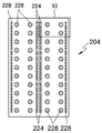
도 6 및 도 7을 참조하면, 인쇄회로기판(102)에는 가장자리를 따라 형성된 제2 본드핑거(130) 및 제2 솔더볼패드(122)가 존재한다. 본 발명의 제1 실시예에 의한 와이어 본딩을 통해 팬 아웃 구조를 달성하는 반도체 패키지(100)는, 상기 제1 본드핑거(128)와 인쇄회로기판(102)에 있는 제2 본드핑거(130)를 도 7과 같이 연결하는 와이어(118)를 포함한다. 6 and 7, the printed
따라서 반도체 칩(104) 내부에서 반도체 칩의 크기 축소로 인해 팬 인(Fan-in) 구조의 제1 솔더볼패드(126)로 형성되지 못한 잔여 본드패드는, 팬 아웃(fan-out) 구조로 제2 솔더볼패드(122)와 연결된다. 이를 상세히 설명하면, 반도체 칩(104)의 잔여 본드패드(124)는 본드패드 재배치 패턴(132)을 통해 제1 본드핑거(128)와 연결된다. 그리고 제1 본드핑거(128)는 와이어(118)를 통해 인쇄회로기판 (102)의 가장자리에 형성된 제2 본드핑거(130)로 연결되고, 다시 배선(134)을 통해 제2 솔더볼패드(122)로 연결된다. 따라서 제2 솔더볼패드(122)의 개수와 제1 및 제2 본드핑거(128, 130)의 개수는 각각 동일하다. Therefore, the remaining bond pads, which are not formed by the first
도 8은 본 발명의 제1 실시예에 대한 변형예를 설명하기 위해 도시한 단면도이다.8 is a cross-sectional view for explaining the modification of the first embodiment of the present invention.
도 8을 참조하면, 상술한 실시예에서는 인쇄회로기판(102)의 바닥에 접착테이프(106)와 같은 접착수단을 사용하여 반도체 칩(104)과 인쇄회로기판(102)을 서로 접착시켰다. 그러나 본 변형예는 상기 접착수단으로 접착테이프 대신에 접착성을 갖는 열전달물질(TIM: Thermal Interface Material)을 사용하는 것이다. 이 경우 상기 인쇄회로기판(102)은 솔더볼패드(122)가 형성된 제1면의 반대면인 제2면에 구리 및 알루미늄과 같이 열전달 특성이 우수한 물질로 형성된 방열판(136)을 추가로 포함할 수 있다. 따라서 반도체 칩(104)이 고속으로 동작할 때, 많은 열을 발생하더라도 반도체 칩(104) 바닥면에서 열전달물질(107)로, 다시 열전달물질(107)에서 방열판(136)으로 연결되는 열전달 경로를 확보하여 외부로 열방출이 용이하다.Referring to FIG. 8, in the above-described embodiment, the
도 9는 본 발명의 제2 실시예에 의한 반도체 패키지를 설명하기 위한 단면도이다.9 is a cross-sectional view for describing the semiconductor package according to the second embodiment of the present invention.
도 9를 참조하면, 본 발명의 제2 실시예에 의한 와이어 본딩을 통해 팬 아웃 구조를 달성하는 반도체 패키지(200)는, 제1면(60)의 가장자리를 따라 복수개의 제2 본드 핑거 및 제2 솔더볼패드(222)가 마련되고 중앙에는 반도체 칩이 들어갈 수 있는 리세스 칩 패드가 형성된 다층 인쇄회로기판(202)을 기본 프레임(base frame)으로 사용하다. Referring to FIG. 9, a
그리고 반도체 칩(204)이 상기 인쇄회로기판(202)의 제1면에 있는 리세스 칩 패드에 접착테이프(206)와 같은 접착수단을 통해 탑재된다. 상기 반도체 칩(204)은 표면에 제1 솔더볼패드와 제1 본드핑거가 형성된 WLCSP형 반도체 칩이다. The
그리고 본 발명의 제2 실시예에 의한 와이어 본딩을 통해 팬 아웃 구조를 달성하는 반도체 패키지(200)는, 상기 제1 및 제2 솔더볼패드가 다층 인쇄회로기판(202)의 배선(234)을 통해 연결되어 제2면(70)으로 확장된 제3 솔더볼패드(238)를 포함한다. 그리고 상기 제1 본드핑거와 상기 제2 본드핑거를 연결하는 와이어(218)와, 상기 와이어(218)를 밀봉하는 엔캡슐런트(encapsulant, 220) 및 상기 제1 및 제2 솔더볼패드(122)에 부착된 솔더볼(216)을 포함한다. In the
상술한 제1 실시예와 비교하여 가장 큰 차이점은 다층의 인쇄회로기판(202)을 기본 프레임으로 사용하는 것과, 제1면(60)에 있는 제1 및 제2 솔더볼패드가 제2면(70)으로 확장된 형태의 제3 솔더볼패드(238)를 더 포함한다는 것이다. 이로 인하여 적층형 반도체 패키지를 만들 수 있다.The biggest difference compared to the first embodiment described above is that the multilayer printed
도 10은 도9의 반도체 칩에 대한 평면도이고, 도 11은 도10의 XI부분에 대한 배선 연결을 설명하기 위해 도시한 확대 평면도이다.FIG. 10 is a plan view of the semiconductor chip of FIG. 9, and FIG. 11 is an enlarged plan view illustrating the wiring connection of the XI part of FIG. 10.
도 10 및 도 11을 참조하면, 원래 반도체 칩(204)에 있는 본드패드(224)는 각각 본드패드 재배치 패턴(232)을 통해 도 11에 도시된 바와 같이 각각 제1 솔더볼패드(226) 및 제1 본드핑거(228)로 연결된다. 이때 상술한 제1 실시예는 한 개 의 줄(row)에서 하나의 본드패드(224)만이 제1 본드핑거(228)와 연결되었다. 그러나 제2 실시예에서는 모든 본드패드(224)가 각각 1:1로 대응하는 제1 본드핑거(228)로 연결된다는 점에서 제1 실시예의 도4와 차이점을 나타낸다. 이는 도9에서는 나타난 바와 같이 제1 솔더볼패드(226)및 제2 솔더볼패드가 다층 인쇄회로기판(202)의 배선(234)을 통해 제3 솔더볼패드(238)로 확장되기 위해서이다.Referring to FIGS. 10 and 11, the
도 12는 도9의 반도체 패키지에서 반도체 칩을 탑재한 후의 밑면도이고, 도 13은 도9의 반도체 패키지에 대한 평면도이다.12 is a bottom view of a semiconductor chip after mounting the semiconductor chip of FIG. 9, and FIG. 13 is a plan view of the semiconductor package of FIG. 9.
도 12 및 도 13을 참조하면, 상기 다층 인쇄회로기판(202)의 제1면(60)은 가장자리를 따라 복수개의 제2 본드 핑거(230) 및 제2 솔더볼패드(222)가 각각 형성되어 있다. 이때 상기 제1 및 제2 본드핑거(228, 230) 각각의 개수는 상기 제1 및 제2 솔더볼패드(226, 222)를 더한 개수와 같게 된다. 즉 상술한 제1 실시예와 비교하여 제1 및 제2 본드핑거(228, 230)의 개수는 상대적으로 증가된다. 12 and 13, a plurality of
이때 반도체 패키지(200)의 전기적 연결은 본드패드(224)에서 제1 솔더볼패드(226) 및 제1 본드핑거(228)로 연결된다. 그 후 반도체 패키지(200)의 전기적 연결은 제1 솔더볼패드(226) 및 제1 본드핑거(228)에서 인쇄회로기판(202)의 제2 본드핑거(230) 및 제2 솔더볼패드(220)로 연결된 후, 마지막으로 다층 인쇄회로기판(202)의 배선(도9의 234)을 통해 제2면(70)의 제3 솔더볼패드(238)로 연결된다. 이에 따라 제2 솔더볼패드(238)의 위치는 상기 인쇄회로기판(202) 내부에서 상기 제1 및 제2 솔더볼패드(226, 222)의 위치와 서로 대응하게 된다.In this case, the electrical connection of the
도 14는 도12의 A부분에 대한 배선 연결을 설명하기 위한 확대 평면도이고, 도 15는 도13의 B 부분에 대한 배선 연결을 설명하기 위한 확대 평면도이다.FIG. 14 is an enlarged plan view for explaining the wiring connection to the portion A of FIG. 12, and FIG. 15 is an enlarged plan view for explaining the wiring connection to the portion B of FIG.
도 14 및 도 15를 참조하면, 본 발명의 제2 실시예에 의한 와이어 본딩을 통해 팬 아웃 구조를 달성하는 반도체 패키지(200)는, 다층 인쇄회로기판(202)의 제1면(도14의 A)에서 제2 본드핑거(230) 및 제2 솔더볼패드(222)로 배선이 연결된다. 그리고 관통 홀(through hole, 240)을 통해 인쇄회로기판(202)의 제2면으로 전기적 연결이 확장된다. 그리고 상기 제2면(도15의 B)에 있는 관통홀(240)은 각각 제3 솔더볼패드(238)로 배선(234)을 통해 전기적으로 연결된다.14 and 15, a
도 16은 본 발명의 제2 실시예에 대한 변형예를 설명하기 위한 단면도이다.16 is a cross-sectional view for explaining a modification to the second embodiment of the present invention.
도 16을 참조하면, 하부에는 도 9에서 설명된 본 발명의 제2 실시예에 의한 반도체 패키지(200)가 있고, 그 상부에는 제3 솔더볼패드를 통해 전기적으로 접속된 본 발명의 제1 실시예에 의한 반도체 패키지(도3의 100)가 상하로 적층되어 있다. 따라서 반도체 패키지가 메모리 소자인 경우, 메모리 소자의 대용량화(high density solution)를 구현할 수 있고, 약간의 변형에 의해 SIP(System In Package)의 구현도 가능하게 된다.Referring to FIG. 16, there is a
도 17은 본 발명의 제2 실시예에 대한 다른 변형예를 설명하기 위해 도시한 단면도이다.17 is a cross-sectional view illustrating another modified example of the second embodiment of the present invention.
도 17을 참조하면, 하부에는 도 9에서 설명된 본 발명의 제2 실시예에 의한 반도체 패키지(200)가 있고, 그 상부에는 본 발명의 제1 실시예의 변형예에 의한 반도체 패키지(도8의 101)가 적층되어 있다. 따라서 적층형 반도체 패키지에서 열 방출 특성을 개선할 수 있는 장점이 있다.Referring to FIG. 17, the
도 18 내지 도 22는 본 발명의 제1 실시예에 의한 반도체 패키지의 제조방법을 설명하기 위해 도시한 단면도들이다.18 to 22 are cross-sectional views illustrating a method of manufacturing a semiconductor package in accordance with a first embodiment of the present invention.
도 18내지 도 22를 참조하면, 먼저 WLCSP형 반도체 칩(104)을 준비한다. 상기 반도체 칩(104)에는 본드패드 재배치 패턴(112)의 일부가 제2 절연막(114)에 의해 노출된 제1 솔더볼패드(126)와 제1 본드패드(128)가 각각 형성되어 있다. 또한 반도체 칩(104) 밑면에는 접착테이프(106)가 부착되어 있다. 이어서 상기 반도체 칩(104)을 단층 인쇄회로기판(102)의 리세스 된 칩 패드에 접착테이프(106)를 통해 탑재한다. 상기 단층 인쇄회로기판(102)의 가장자리에는 제2 본드핑거(130) 및 제2 솔더볼패드(122)가 각각 형성되어 있다.18 to 22, a WLCSP
이어서 상기 제1 본드핑거(128) 및 제2 본드핑거(130)를 와이어(118)로 연결하는 와이어 본딩 공정을 진행하고, 상기 와이어(118)를 엔캡슐런트(encapsulant, 120)로 밀봉한다. 마지막으로 상기 제1 및 제2 솔더볼패드(126, 122)에 솔더볼(116)을 부착한다.Subsequently, a wire bonding process of connecting the
본 발명의 제2 실시예에 의한 와이어 본딩을 통해 팬 아웃 구조를 달성하는 반도체 패키지(200)의 제조방법 역시, 인쇄회로기판(202) 및 반도체 칩(204)의 구조만 약간 차이가 있을 뿐, 전반적인 패키징 공정이 상술한 제1 실시예와 유사하기 때문에 중복을 피하여 설명을 생략한다.In the manufacturing method of the
본 발명은 상기한 실시예에 한정되지 않으며, 본 발명이 속한 기술적 사상 내에서 당 분야의 통상의 지식을 가진 자에 의해 많은 변형이 가능함이 명백하다.The present invention is not limited to the above embodiments, and it is apparent that many modifications can be made by those skilled in the art within the technical spirit to which the present invention belongs.
따라서, 상술한 본 발명에 따르면, 첫째 WLCSP 형태의 반도체 칩의 크기가 줄어들더라도 와이어 본딩을 통해 솔더볼을 팬 아웃(fan-out) 구조로 장착하는 것이 가능하다. 둘째 두꺼운 재질의 인쇄회로기판을 사용하기 때문에 휨(warpage) 및 크랙(crack) 결함이 발생하는 것을 억제하면서 몰딩 공정을 생략할 수 있다. 셋째 인쇄회로기판에 추가로 방열판을 설치하여 고속으로 동작하는 반도체 소자의 열방출에 유리하다. 넷째 효과적인 적층형 반도체 패키지를 구현하여 SIP(System In Package)를 만들거나, 반도체 소자의 집적도를 높일 수 있다.Therefore, according to the present invention described above, even if the size of the first WLCSP-type semiconductor chip is reduced, it is possible to mount the solder ball in a fan-out structure through wire bonding. Second, since a thick printed circuit board is used, the molding process can be omitted while suppressing warpage and crack defects. Third, it is advantageous to heat dissipation of a semiconductor device that operates at a high speed by installing a heat sink in addition to the printed circuit board. Fourth, an effective stacked semiconductor package may be implemented to make a system in package (SIP) or to increase the degree of integration of semiconductor devices.
Claims (20)
Priority Applications (4)
| Application Number | Priority Date | Filing Date | Title |
|---|---|---|---|
| KR1020050030736A KR100618892B1 (en) | 2005-04-13 | 2005-04-13 | Semiconductor package achieves fan-out structure through wire bonding |
| US11/279,344 US7327032B2 (en) | 2005-04-13 | 2006-04-11 | Semiconductor package accomplishing fan-out structure through wire bonding |
| US11/954,707 US7550830B2 (en) | 2005-04-13 | 2007-12-12 | Stacked semiconductor package having fan-out structure through wire bonding |
| US12/434,568 US20090212412A1 (en) | 2005-04-13 | 2009-05-01 | Semiconductor package accomplishing fan-out structure through wire bonding |
Applications Claiming Priority (1)
| Application Number | Priority Date | Filing Date | Title |
|---|---|---|---|
| KR1020050030736A KR100618892B1 (en) | 2005-04-13 | 2005-04-13 | Semiconductor package achieves fan-out structure through wire bonding |
Publications (1)
| Publication Number | Publication Date |
|---|---|
| KR100618892B1 true KR100618892B1 (en) | 2006-09-01 |
Family
ID=37107729
Family Applications (1)
| Application Number | Title | Priority Date | Filing Date |
|---|---|---|---|
| KR1020050030736A Expired - Fee Related KR100618892B1 (en) | 2005-04-13 | 2005-04-13 | Semiconductor package achieves fan-out structure through wire bonding |
Country Status (2)
| Country | Link |
|---|---|
| US (3) | US7327032B2 (en) |
| KR (1) | KR100618892B1 (en) |
Cited By (4)
| Publication number | Priority date | Publication date | Assignee | Title |
|---|---|---|---|---|
| KR100959604B1 (en) * | 2008-03-10 | 2010-05-27 | 주식회사 하이닉스반도체 | Wafer level semiconductor package and method for manufacturing same |
| US8018043B2 (en) | 2008-03-10 | 2011-09-13 | Hynix Semiconductor Inc. | Semiconductor package having side walls and method for manufacturing the same |
| US9202716B2 (en) | 2011-12-09 | 2015-12-01 | Samsung Electronics Co., Ltd. | Methods of fabricating fan-out wafer level packages and packages formed by the methods |
| KR20210101574A (en) * | 2020-02-10 | 2021-08-19 | 삼성전자주식회사 | Semiconductor packages and method of manufacturing semiconductor packages |
Families Citing this family (52)
| Publication number | Priority date | Publication date | Assignee | Title |
|---|---|---|---|---|
| JP3602968B2 (en) * | 1998-08-18 | 2004-12-15 | 沖電気工業株式会社 | Semiconductor device and substrate connection structure thereof |
| US7633765B1 (en) | 2004-03-23 | 2009-12-15 | Amkor Technology, Inc. | Semiconductor package including a top-surface metal layer for implementing circuit features |
| US7548430B1 (en) | 2002-05-01 | 2009-06-16 | Amkor Technology, Inc. | Buildup dielectric and metallization process and semiconductor package |
| US9691635B1 (en) | 2002-05-01 | 2017-06-27 | Amkor Technology, Inc. | Buildup dielectric layer having metallization pattern semiconductor package fabrication method |
| US10811277B2 (en) | 2004-03-23 | 2020-10-20 | Amkor Technology, Inc. | Encapsulated semiconductor package |
| US11081370B2 (en) | 2004-03-23 | 2021-08-03 | Amkor Technology Singapore Holding Pte. Ltd. | Methods of manufacturing an encapsulated semiconductor device |
| KR100618892B1 (en) * | 2005-04-13 | 2006-09-01 | 삼성전자주식회사 | Semiconductor package achieves fan-out structure through wire bonding |
| KR100762423B1 (en) * | 2006-06-27 | 2007-10-02 | 박영진 | Semiconductor package and manufacturing method thereof |
| JP5042591B2 (en) * | 2006-10-27 | 2012-10-03 | 新光電気工業株式会社 | Semiconductor package and stacked semiconductor package |
| US7550857B1 (en) * | 2006-11-16 | 2009-06-23 | Amkor Technology, Inc. | Stacked redistribution layer (RDL) die assembly package |
| KR100887475B1 (en) * | 2007-02-26 | 2009-03-10 | 주식회사 네패스 | Semiconductor package and manufacturing method |
| US20090032972A1 (en) * | 2007-03-30 | 2009-02-05 | Kabushiki Kaisha Toshiba | Semiconductor device |
| US7868441B2 (en) | 2007-04-13 | 2011-01-11 | Maxim Integrated Products, Inc. | Package on-package secure module having BGA mesh cap |
| US7923830B2 (en) * | 2007-04-13 | 2011-04-12 | Maxim Integrated Products, Inc. | Package-on-package secure module having anti-tamper mesh in the substrate of the upper package |
| KR100826989B1 (en) * | 2007-06-20 | 2008-05-02 | 주식회사 하이닉스반도체 | Semiconductor package and manufacturing method thereof |
| US7619901B2 (en) * | 2007-06-25 | 2009-11-17 | Epic Technologies, Inc. | Integrated structures and fabrication methods thereof implementing a cell phone or other electronic system |
| US8241954B2 (en) * | 2007-12-03 | 2012-08-14 | Stats Chippac, Ltd. | Wafer level die integration and method |
| US8076786B2 (en) * | 2008-07-11 | 2011-12-13 | Advanced Semiconductor Engineering, Inc. | Semiconductor package and method for packaging a semiconductor package |
| WO2010013470A1 (en) * | 2008-07-31 | 2010-02-04 | 三洋電機株式会社 | Semiconductor module and portable apparatus provided with semiconductor module |
| US8198547B2 (en) | 2009-07-23 | 2012-06-12 | Lexmark International, Inc. | Z-directed pass-through components for printed circuit boards |
| KR101113501B1 (en) * | 2009-11-12 | 2012-02-29 | 삼성전기주식회사 | Manufacturing method of semiconductor package |
| US8169065B2 (en) * | 2009-12-22 | 2012-05-01 | Epic Technologies, Inc. | Stackable circuit structures and methods of fabrication thereof |
| US20110156240A1 (en) * | 2009-12-31 | 2011-06-30 | Stmicroelectronics Asia Pacific Pte. Ltd. | Reliable large die fan-out wafer level package and method of manufacture |
| US8884422B2 (en) * | 2009-12-31 | 2014-11-11 | Stmicroelectronics Pte Ltd. | Flip-chip fan-out wafer level package for package-on-package applications, and method of manufacture |
| US8436255B2 (en) * | 2009-12-31 | 2013-05-07 | Stmicroelectronics Pte Ltd. | Fan-out wafer level package with polymeric layer for high reliability |
| US8502394B2 (en) * | 2009-12-31 | 2013-08-06 | Stmicroelectronics Pte Ltd. | Multi-stacked semiconductor dice scale package structure and method of manufacturing same |
| US8466997B2 (en) * | 2009-12-31 | 2013-06-18 | Stmicroelectronics Pte Ltd. | Fan-out wafer level package for an optical sensor and method of manufacture thereof |
| JP5115573B2 (en) * | 2010-03-03 | 2013-01-09 | オムロン株式会社 | Method for manufacturing connection pad |
| CN102208396A (en) * | 2010-03-30 | 2011-10-05 | 日月光半导体制造股份有限公司 | Semiconductor package and method of manufacturing the same |
| US8598695B2 (en) * | 2010-07-23 | 2013-12-03 | Tessera, Inc. | Active chip on carrier or laminated chip having microelectronic element embedded therein |
| US8847376B2 (en) * | 2010-07-23 | 2014-09-30 | Tessera, Inc. | Microelectronic elements with post-assembly planarization |
| US8525344B2 (en) | 2011-02-24 | 2013-09-03 | Stats Chippac, Ltd. | Semiconductor device and method of forming bond wires between semiconductor die contact pads and conductive TOV in peripheral area around semiconductor die |
| US8644999B2 (en) * | 2011-06-15 | 2014-02-04 | General Electric Company | Keep alive method for RFD devices |
| CN102866279A (en) * | 2011-07-04 | 2013-01-09 | 新科实业有限公司 | Current sensor device |
| US8943684B2 (en) | 2011-08-31 | 2015-02-03 | Lexmark International, Inc. | Continuous extrusion process for manufacturing a Z-directed component for a printed circuit board |
| US9009954B2 (en) | 2011-08-31 | 2015-04-21 | Lexmark International, Inc. | Process for manufacturing a Z-directed component for a printed circuit board using a sacrificial constraining material |
| US9078374B2 (en) * | 2011-08-31 | 2015-07-07 | Lexmark International, Inc. | Screening process for manufacturing a Z-directed component for a printed circuit board |
| US9013037B2 (en) | 2011-09-14 | 2015-04-21 | Stmicroelectronics Pte Ltd. | Semiconductor package with improved pillar bump process and structure |
| ITMI20111777A1 (en) * | 2011-09-30 | 2013-03-31 | St Microelectronics Srl | ELECTRONIC WELDING SYSTEM |
| US8779601B2 (en) | 2011-11-02 | 2014-07-15 | Stmicroelectronics Pte Ltd | Embedded wafer level package for 3D and package-on-package applications, and method of manufacture |
| US8916481B2 (en) | 2011-11-02 | 2014-12-23 | Stmicroelectronics Pte Ltd. | Embedded wafer level package for 3D and package-on-package applications, and method of manufacture |
| KR101488590B1 (en) | 2013-03-29 | 2015-01-30 | 앰코 테크놀로지 코리아 주식회사 | Semiconductor device and manufacturing method thereof |
| WO2015077808A1 (en) | 2013-11-27 | 2015-06-04 | At&S Austria Technologie & Systemtechnik Aktiengesellschaft | Circuit board structure |
| AT515101B1 (en) | 2013-12-12 | 2015-06-15 | Austria Tech & System Tech | Method for embedding a component in a printed circuit board |
| US11523520B2 (en) | 2014-02-27 | 2022-12-06 | At&S Austria Technologie & Systemtechnik Aktiengesellschaft | Method for making contact with a component embedded in a printed circuit board |
| KR102437687B1 (en) * | 2015-11-10 | 2022-08-26 | 삼성전자주식회사 | Semiconductor devices and semicinductor packages thereof |
| KR102049255B1 (en) * | 2016-06-20 | 2019-11-28 | 삼성전자주식회사 | Fan-out semiconductor package |
| US10109617B2 (en) * | 2016-07-21 | 2018-10-23 | Samsung Electronics Co., Ltd. | Solid state drive package |
| KR102404058B1 (en) | 2017-12-28 | 2022-05-31 | 삼성전자주식회사 | Semiconductor package |
| US11410875B2 (en) * | 2018-12-19 | 2022-08-09 | Texas Instruments Incorporated | Fan-out electronic device |
| US11721657B2 (en) | 2019-06-14 | 2023-08-08 | Stmicroelectronics Pte Ltd | Wafer level chip scale package having varying thicknesses |
| KR102807817B1 (en) | 2020-01-15 | 2025-05-14 | 삼성전자주식회사 | Semiconductor devices |
Citations (2)
| Publication number | Priority date | Publication date | Assignee | Title |
|---|---|---|---|---|
| KR20000029367A (en) * | 1998-10-29 | 2000-05-25 | 포만 제프리 엘 | Deep divot mask for enhanced buried-channel pfet performance and reliability |
| KR20000028356A (en) * | 1998-10-31 | 2000-05-25 | 김규현 | Semiconductor package |
Family Cites Families (28)
| Publication number | Priority date | Publication date | Assignee | Title |
|---|---|---|---|---|
| US5888837A (en) * | 1996-04-16 | 1999-03-30 | General Electric Company | Chip burn-in and test structure and method |
| KR100266637B1 (en) * | 1997-11-15 | 2000-09-15 | 김영환 | Stackable ball grid array semiconductor package and a method thereof |
| US6133634A (en) * | 1998-08-05 | 2000-10-17 | Fairchild Semiconductor Corporation | High performance flip chip package |
| JP3825181B2 (en) * | 1998-08-20 | 2006-09-20 | 沖電気工業株式会社 | Semiconductor device manufacturing method and semiconductor device |
| US6313522B1 (en) * | 1998-08-28 | 2001-11-06 | Micron Technology, Inc. | Semiconductor structure having stacked semiconductor devices |
| US6219254B1 (en) * | 1999-04-05 | 2001-04-17 | Trw Inc. | Chip-to-board connection assembly and method therefor |
| KR20000074142A (en) | 1999-05-18 | 2000-12-05 | 김영환 | Semiconductor package and Method for fabricating the same |
| KR100333388B1 (en) * | 1999-06-29 | 2002-04-18 | 박종섭 | chip size stack package and method of fabricating the same |
| KR20010046832A (en) | 1999-11-16 | 2001-06-15 | 박종섭 | Chip Scale Package |
| TW522531B (en) * | 2000-10-20 | 2003-03-01 | Matsushita Electric Industrial Co Ltd | Semiconductor device, method of manufacturing the device and mehtod of mounting the device |
| US6537848B2 (en) * | 2001-05-30 | 2003-03-25 | St. Assembly Test Services Ltd. | Super thin/super thermal ball grid array package |
| US7332819B2 (en) * | 2002-01-09 | 2008-02-19 | Micron Technology, Inc. | Stacked die in die BGA package |
| TW557521B (en) * | 2002-01-16 | 2003-10-11 | Via Tech Inc | Integrated circuit package and its manufacturing process |
| US6650015B2 (en) * | 2002-02-05 | 2003-11-18 | Siliconware Precision Industries Co., Ltd. | Cavity-down ball grid array package with semiconductor chip solder ball |
| KR100485111B1 (en) | 2002-07-31 | 2005-04-27 | 앰코 테크놀로지 코리아 주식회사 | chip size package |
| JP4365108B2 (en) * | 2003-01-08 | 2009-11-18 | 浜松ホトニクス株式会社 | Wiring board and radiation detector using the same |
| TWI246761B (en) * | 2003-05-14 | 2006-01-01 | Siliconware Precision Industries Co Ltd | Semiconductor package with build-up layers formed on chip and fabrication method of the semiconductor package |
| TWI253155B (en) * | 2003-05-28 | 2006-04-11 | Siliconware Precision Industries Co Ltd | Thermally enhanced semiconductor package and fabrication method thereof |
| TWI255538B (en) * | 2003-06-09 | 2006-05-21 | Siliconware Precision Industries Co Ltd | Semiconductor package having conductive bumps on chip and method for fabricating the same |
| JP2005175423A (en) * | 2003-11-18 | 2005-06-30 | Denso Corp | Semiconductor package |
| US6949823B2 (en) * | 2004-01-30 | 2005-09-27 | Agilent Technologies, Inc. | Method and apparatus for high electrical and thermal performance ball grid array package |
| US7208344B2 (en) * | 2004-03-31 | 2007-04-24 | Aptos Corporation | Wafer level mounting frame for ball grid array packaging, and method of making and using the same |
| US7411281B2 (en) * | 2004-06-21 | 2008-08-12 | Broadcom Corporation | Integrated circuit device package having both wire bond and flip-chip interconnections and method of making the same |
| US7786591B2 (en) * | 2004-09-29 | 2010-08-31 | Broadcom Corporation | Die down ball grid array package |
| US7217994B2 (en) * | 2004-12-01 | 2007-05-15 | Kyocera Wireless Corp. | Stack package for high density integrated circuits |
| KR100618892B1 (en) * | 2005-04-13 | 2006-09-01 | 삼성전자주식회사 | Semiconductor package achieves fan-out structure through wire bonding |
| SG135074A1 (en) * | 2006-02-28 | 2007-09-28 | Micron Technology Inc | Microelectronic devices, stacked microelectronic devices, and methods for manufacturing such devices |
| US7635913B2 (en) * | 2006-12-09 | 2009-12-22 | Stats Chippac Ltd. | Stacked integrated circuit package-in-package system |
-
2005
- 2005-04-13 KR KR1020050030736A patent/KR100618892B1/en not_active Expired - Fee Related
-
2006
- 2006-04-11 US US11/279,344 patent/US7327032B2/en active Active
-
2007
- 2007-12-12 US US11/954,707 patent/US7550830B2/en active Active
-
2009
- 2009-05-01 US US12/434,568 patent/US20090212412A1/en not_active Abandoned
Patent Citations (2)
| Publication number | Priority date | Publication date | Assignee | Title |
|---|---|---|---|---|
| KR20000029367A (en) * | 1998-10-29 | 2000-05-25 | 포만 제프리 엘 | Deep divot mask for enhanced buried-channel pfet performance and reliability |
| KR20000028356A (en) * | 1998-10-31 | 2000-05-25 | 김규현 | Semiconductor package |
Cited By (5)
| Publication number | Priority date | Publication date | Assignee | Title |
|---|---|---|---|---|
| KR100959604B1 (en) * | 2008-03-10 | 2010-05-27 | 주식회사 하이닉스반도체 | Wafer level semiconductor package and method for manufacturing same |
| US8018043B2 (en) | 2008-03-10 | 2011-09-13 | Hynix Semiconductor Inc. | Semiconductor package having side walls and method for manufacturing the same |
| US9202716B2 (en) | 2011-12-09 | 2015-12-01 | Samsung Electronics Co., Ltd. | Methods of fabricating fan-out wafer level packages and packages formed by the methods |
| KR20210101574A (en) * | 2020-02-10 | 2021-08-19 | 삼성전자주식회사 | Semiconductor packages and method of manufacturing semiconductor packages |
| KR102736602B1 (en) | 2020-02-10 | 2024-12-02 | 삼성전자주식회사 | Semiconductor packages and method of manufacturing semiconductor packages |
Also Published As
| Publication number | Publication date |
|---|---|
| US7327032B2 (en) | 2008-02-05 |
| US7550830B2 (en) | 2009-06-23 |
| US20060231950A1 (en) | 2006-10-19 |
| US20090212412A1 (en) | 2009-08-27 |
| US20080088018A1 (en) | 2008-04-17 |
Similar Documents
| Publication | Publication Date | Title |
|---|---|---|
| KR100618892B1 (en) | Semiconductor package achieves fan-out structure through wire bonding | |
| US7298033B2 (en) | Stack type ball grid array package and method for manufacturing the same | |
| KR100493063B1 (en) | BGA package with stacked semiconductor chips and manufacturing method thereof | |
| US8253232B2 (en) | Package on package having a conductive post with height lower than an upper surface of an encapsulation layer to prevent circuit pattern lift defect and method of fabricating the same | |
| US8183687B2 (en) | Interposer for die stacking in semiconductor packages and the method of making the same | |
| US7902650B2 (en) | Semiconductor package and method for manufacturing the same | |
| KR20190079065A (en) | Interposer substrate and semiconductor package | |
| CN101038908A (en) | Stack package utilizing through vias and re-distribution lines | |
| TWI430425B (en) | Integrated circuit package system using bump technology | |
| CN100585839C (en) | Chip packaging structure and chip packaging process | |
| US7235870B2 (en) | Microelectronic multi-chip module | |
| CN110246812A (en) | A kind of semiconductor package and preparation method thereof | |
| US20140097530A1 (en) | Integrated circuit package | |
| US20070052082A1 (en) | Multi-chip package structure | |
| KR20130050077A (en) | Stacked Packages and Methods for Manufacturing the Same | |
| KR20080048311A (en) | Semiconductor package and manufacturing method | |
| KR19980025890A (en) | Multi-chip package with lead frame | |
| KR100780690B1 (en) | Manufacturing method of stack package | |
| CN2531525Y (en) | Direct cooling type BGA substrate | |
| KR20080074654A (en) | Laminated Semiconductor Packages | |
| US8399967B2 (en) | Package structure | |
| KR20110137060A (en) | Semiconductor package | |
| KR100421777B1 (en) | semiconductor package | |
| KR20080084075A (en) | Laminated Semiconductor Packages | |
| CN100459124C (en) | Multi-chip packaging structure |
Legal Events
| Date | Code | Title | Description |
|---|---|---|---|
| A201 | Request for examination | ||
| PA0109 | Patent application |
St.27 status event code: A-0-1-A10-A12-nap-PA0109 |
|
| PA0201 | Request for examination |
St.27 status event code: A-1-2-D10-D11-exm-PA0201 |
|
| R17-X000 | Change to representative recorded |
St.27 status event code: A-3-3-R10-R17-oth-X000 |
|
| PN2301 | Change of applicant |
St.27 status event code: A-3-3-R10-R13-asn-PN2301 St.27 status event code: A-3-3-R10-R11-asn-PN2301 |
|
| PN2301 | Change of applicant |
St.27 status event code: A-3-3-R10-R13-asn-PN2301 St.27 status event code: A-3-3-R10-R11-asn-PN2301 |
|
| D13-X000 | Search requested |
St.27 status event code: A-1-2-D10-D13-srh-X000 |
|
| D14-X000 | Search report completed |
St.27 status event code: A-1-2-D10-D14-srh-X000 |
|
| E701 | Decision to grant or registration of patent right | ||
| PE0701 | Decision of registration |
St.27 status event code: A-1-2-D10-D22-exm-PE0701 |
|
| GRNT | Written decision to grant | ||
| PR0701 | Registration of establishment |
St.27 status event code: A-2-4-F10-F11-exm-PR0701 |
|
| PR1002 | Payment of registration fee |
St.27 status event code: A-2-2-U10-U11-oth-PR1002 Fee payment year number: 1 |
|
| PG1601 | Publication of registration |
St.27 status event code: A-4-4-Q10-Q13-nap-PG1601 |
|
| PR1001 | Payment of annual fee |
St.27 status event code: A-4-4-U10-U11-oth-PR1001 Fee payment year number: 4 |
|
| PR1001 | Payment of annual fee |
St.27 status event code: A-4-4-U10-U11-oth-PR1001 Fee payment year number: 5 |
|
| PR1001 | Payment of annual fee |
St.27 status event code: A-4-4-U10-U11-oth-PR1001 Fee payment year number: 6 |
|
| R18-X000 | Changes to party contact information recorded |
St.27 status event code: A-5-5-R10-R18-oth-X000 |
|
| FPAY | Annual fee payment |
Payment date: 20120801 Year of fee payment: 7 |
|
| PR1001 | Payment of annual fee |
St.27 status event code: A-4-4-U10-U11-oth-PR1001 Fee payment year number: 7 |
|
| FPAY | Annual fee payment |
Payment date: 20130731 Year of fee payment: 8 |
|
| PR1001 | Payment of annual fee |
St.27 status event code: A-4-4-U10-U11-oth-PR1001 Fee payment year number: 8 |
|
| FPAY | Annual fee payment |
Payment date: 20140731 Year of fee payment: 9 |
|
| PR1001 | Payment of annual fee |
St.27 status event code: A-4-4-U10-U11-oth-PR1001 Fee payment year number: 9 |
|
| PR1001 | Payment of annual fee |
St.27 status event code: A-4-4-U10-U11-oth-PR1001 Fee payment year number: 10 |
|
| FPAY | Annual fee payment |
Payment date: 20160801 Year of fee payment: 11 |
|
| PR1001 | Payment of annual fee |
St.27 status event code: A-4-4-U10-U11-oth-PR1001 Fee payment year number: 11 |
|
| PR1001 | Payment of annual fee |
St.27 status event code: A-4-4-U10-U11-oth-PR1001 Fee payment year number: 12 |
|
| FPAY | Annual fee payment |
Payment date: 20180731 Year of fee payment: 13 |
|
| PR1001 | Payment of annual fee |
St.27 status event code: A-4-4-U10-U11-oth-PR1001 Fee payment year number: 13 |
|
| FPAY | Annual fee payment |
Payment date: 20190731 Year of fee payment: 14 |
|
| PR1001 | Payment of annual fee |
St.27 status event code: A-4-4-U10-U11-oth-PR1001 Fee payment year number: 14 |
|
| PR1001 | Payment of annual fee |
St.27 status event code: A-4-4-U10-U11-oth-PR1001 Fee payment year number: 15 |
|
| PR1001 | Payment of annual fee |
St.27 status event code: A-4-4-U10-U11-oth-PR1001 Fee payment year number: 16 |
|
| PR1001 | Payment of annual fee |
St.27 status event code: A-4-4-U10-U11-oth-PR1001 Fee payment year number: 17 |
|
| PR1001 | Payment of annual fee |
St.27 status event code: A-4-4-U10-U11-oth-PR1001 Fee payment year number: 18 |
|
| PC1903 | Unpaid annual fee |
St.27 status event code: A-4-4-U10-U13-oth-PC1903 Not in force date: 20240826 Payment event data comment text: Termination Category : DEFAULT_OF_REGISTRATION_FEE |
|
| PC1903 | Unpaid annual fee |
St.27 status event code: N-4-6-H10-H13-oth-PC1903 Ip right cessation event data comment text: Termination Category : DEFAULT_OF_REGISTRATION_FEE Not in force date: 20240826 |
|
| P22-X000 | Classification modified |
St.27 status event code: A-4-4-P10-P22-nap-X000 |