KR100595884B1 - Nitride semiconductor device manufacturing method - Google Patents
Nitride semiconductor device manufacturing method Download PDFInfo
- Publication number
- KR100595884B1 KR100595884B1 KR1020040035299A KR20040035299A KR100595884B1 KR 100595884 B1 KR100595884 B1 KR 100595884B1 KR 1020040035299 A KR1020040035299 A KR 1020040035299A KR 20040035299 A KR20040035299 A KR 20040035299A KR 100595884 B1 KR100595884 B1 KR 100595884B1
- Authority
- KR
- South Korea
- Prior art keywords
- nitride semiconductor
- semiconductor unit
- substrate
- bonding
- forming
- Prior art date
- Legal status (The legal status is an assumption and is not a legal conclusion. Google has not performed a legal analysis and makes no representation as to the accuracy of the status listed.)
- Expired - Fee Related
Links
Images


Classifications
-
- H—ELECTRICITY
- H10—SEMICONDUCTOR DEVICES; ELECTRIC SOLID-STATE DEVICES NOT OTHERWISE PROVIDED FOR
- H10H—INORGANIC LIGHT-EMITTING SEMICONDUCTOR DEVICES HAVING POTENTIAL BARRIERS
- H10H20/00—Individual inorganic light-emitting semiconductor devices having potential barriers, e.g. light-emitting diodes [LED]
- H10H20/01—Manufacture or treatment
- H10H20/011—Manufacture or treatment of bodies, e.g. forming semiconductor layers
- H10H20/018—Bonding of wafers
-
- H—ELECTRICITY
- H10—SEMICONDUCTOR DEVICES; ELECTRIC SOLID-STATE DEVICES NOT OTHERWISE PROVIDED FOR
- H10H—INORGANIC LIGHT-EMITTING SEMICONDUCTOR DEVICES HAVING POTENTIAL BARRIERS
- H10H20/00—Individual inorganic light-emitting semiconductor devices having potential barriers, e.g. light-emitting diodes [LED]
- H10H20/80—Constructional details
- H10H20/81—Bodies
- H10H20/813—Bodies having a plurality of light-emitting regions, e.g. multi-junction LEDs or light-emitting devices having photoluminescent regions within the bodies
-
- H—ELECTRICITY
- H10—SEMICONDUCTOR DEVICES; ELECTRIC SOLID-STATE DEVICES NOT OTHERWISE PROVIDED FOR
- H10H—INORGANIC LIGHT-EMITTING SEMICONDUCTOR DEVICES HAVING POTENTIAL BARRIERS
- H10H20/00—Individual inorganic light-emitting semiconductor devices having potential barriers, e.g. light-emitting diodes [LED]
- H10H20/80—Constructional details
- H10H20/81—Bodies
- H10H20/819—Bodies characterised by their shape, e.g. curved or truncated substrates
-
- H10W90/00—
Landscapes
- Led Devices (AREA)
- Semiconductor Lasers (AREA)
- Ceramic Products (AREA)
Abstract
본 발명은 질화물 반도체 소자 제조 방법에 관한 것으로서, 질화물 반도체 단위 소자들을 상호간에 분리시키는 소정의 트렌치에 크랙방지벽을 채워 보이드(void)를 제거함으로써, 레이저 리프트 오프 공정시 질화물 반도체 단위 소자에 발생할 수 있는 크랙(crack)이나 손상(damage)을 최소한으로 줄이도록 하며, 특히 크랙방지벽을 유전체 물질로 형성함으로써 접합공정시 인가되는 열에 의한 트렌치내 소자 계면과의 반응을 줄일 수 있어 소자의 전기적 특성과 광학적 특성이 퇴화되는 것을 방지하고, 자체의 절연적 특성으로 질화물 반도체 단위소자 사이들간에 전기적 절연과 소자의 보호층(protection layer)으로서의 사용이 가능하도록 하며, 또한 도전성 금속을 이용해 형성한 본 발명의 접합강화 판이나 벽을 통해 캐리어 기판에 코팅된 본딩부재와 접합시킴으로써 캐리어 기판과의 강한 접착력을 유지한다.BACKGROUND OF THE INVENTION 1. Field of the Invention The present invention relates to a method for fabricating a nitride semiconductor device, wherein a void is formed by filling a crack prevention wall in a predetermined trench separating nitride semiconductor unit devices from each other, so that the nitride semiconductor unit device may be generated during a laser lift-off process. It minimizes cracks and damages, and it is possible to reduce the reaction with the device interface in the trench due to the heat applied during the bonding process. The optical property of the present invention is prevented from deterioration, and its insulating property enables electrical insulation between the nitride semiconductor unit devices and the use as a protection layer of the device, and is formed using a conductive metal. When bonding with the bonding member coated on the carrier substrate through bonding reinforcement plate or wall By maintains a strong adhesion between the carrier substrate.
소자, 크랙, 방지, 금속, 접합, 유전체, 보이드Device, Crack, Prevent, Metal, Junction, Dielectric, Void
Description
도 1a 내지 도 1i는 본 발명에 따른 질화물 반도체소자 제조 방법의 제1실시예를 도시한 도면,1A to 1I illustrate a first embodiment of a method of manufacturing a nitride semiconductor device according to the present invention;
도 2a 내지 도 2e는 본 발명에 따른 질화물 반도체소자 제조 방법의 제2실시예를 도시한 도면이다.2A to 2E are diagrams illustrating a second embodiment of a method of manufacturing a nitride semiconductor device according to the present invention.
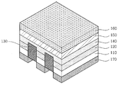
* 도면의 주요 부분에 대한 부호의 설명 *Explanation of symbols on the main parts of the drawings
100 : 사파이어 기판 110 : 질화물 반도체 단위 소자100: sapphire substrate 110: nitride semiconductor unit device
120 : 제1전극 130 : 크랙방지벽120: first electrode 130: crack prevention wall
140 : 접합강화판 150 : 본딩부재140: bonding reinforcing plate 150: bonding member
160 : 캐리어 기판160: carrier substrate
본 발명은 레이저 리프트 오프 공정시 질화물 반도체 단위 소자에 발생할 수 있는 크랙(crack)이나 손상(damage)을 최소한으로 줄이고자 하는 질화물 반도체 소자 제조 방법에 관한 것이다.The present invention relates to a method for manufacturing a nitride semiconductor device to minimize the cracks or damage that can occur in the nitride semiconductor unit device during the laser lift-off process.
일반적으로, 질화물 반도체를 성장시키기 위해 사용되는 기판으로 사파이어 기판을 주로 사용한다. 하지만 이러한 질화물을 이용한 소자제작에 있어 사파이어 자체의 전도성 문제로 인해 소자제조시 많은 어려움이 발생되며, 또한 열전도도가 다른 물질에 비해 현저히 나쁘기 때문에 소자 구동에 있어서도 상당한 문제점을 야기시킨다.In general, a sapphire substrate is mainly used as a substrate used for growing a nitride semiconductor. However, due to the conductivity problem of the sapphire itself in the device fabrication using such a nitride, a lot of difficulties occur during device fabrication, and also because the thermal conductivity is significantly worse than other materials, causing significant problems in device driving.
그래서, 이러한 문제점을 해결하기 위해 기존에는 LLO(laser lift off)방법을 이용하여 왔는데, 하지만 이러한 LLO방법 역시 레이저 빔의 크기와 균일함의 한계로 인해 사파이어 기판 전면을 한번에 제거할 수 없기 때문에 균일하게 제작된 작은 사이즈의 빔을 사파이어 기판에 일부분씩 조사하여 사파이어 전체를 제거하게 되어 있어 이에 따라 빔이 겹치는 부분이 생겨 그러한 부분에서 떨어진 질화물 뒷 표면이 균일하지 못하다는 문제가 발생하게 되며, 또한 일부 막질이 좋지 못한 부분에서 발생할 수 있는 크랙이 다른 부분으로 전파되는 현상이 발생하게 된다.So, in order to solve this problem, the conventional LLO (laser lift off) method has been used, but the LLO method is also manufactured uniformly because the entire surface of the sapphire substrate cannot be removed at once because of the size and uniformity of the laser beam. The small sapphire substrate is partially irradiated onto the sapphire substrate to remove the entire sapphire, resulting in overlapping beams, resulting in a problem that the back surface of the nitride separated from such a portion is not uniform. Cracks, which may occur in bad parts, may spread to other parts.
이러한 현상을 막기 위해 질화물 막의 일부를 에칭하여 소자 각각을 분리한 후, Si, GaAs 등의 기판이나 Cu, Au, Al플레이트에 본딩 후 사파이어 기판을 분리시키는 방법을 사용하게 된다.In order to prevent this phenomenon, a part of the nitride film is etched to separate the devices, and then a method of separating a sapphire substrate after bonding to a substrate such as Si, GaAs, or Cu, Au, or Al plate is used.
하지만, 본딩 후에 각 소자와 소자 사이의 트렌치에 형성된 빈 공간(void)에 에어가 잔존하게 될 경우가 발생하게 되는데, 이러한 에어(air)는 레이저의 강한 열에너지로 인해 팽창되어 주위의 질화물 소자에 크랙(crack)을 발생시키는 원인이 되며, 또한 트렌치(trench)내의 보이드(void)를 제거하기 위해 사용된 종래의 에폭시접합방법의 경우에는 사용된 에폭시가 전류가 통하지 않는 부도체이기 때문에 프 리 스탠딩된 소자를 제조하기 위해서는 부가적으로 2차 접합 공정을 수행해야 하는 번거로움이 발생된다.However, after bonding, air may remain in voids formed in the trenches between the elements and the elements, which are expanded due to the strong thermal energy of the laser and crack in the surrounding nitride elements. In the conventional epoxy bonding method used to cause cracks and to remove voids in the trench, the pre-standing device is used because the epoxy used is a non-current conducting insulator. In order to manufacture the additional inconvenience of having to perform an additional secondary bonding process.
이에 본 발명은 상기한 문제점을 해소시키기 위하여 개발된 것으로, 레이저 리프트 오프 공정시 질화물 반도체 단위 소자에 발생할 수 있는 크랙(crack)이나 손상(damage)을 최소한으로 줄이고자 하는 질화물 반도체 소자 제조 방법을 제공하는데 그 목적이 있다.Accordingly, the present invention has been developed to solve the above problems, and provides a method of manufacturing a nitride semiconductor device to minimize the cracks (damage) or damage (damage) that may occur in the nitride semiconductor unit device during the laser lift-off process. Its purpose is to.
이러한 목적에 따라 본 발명은, 첫 번째로 질화물 반도체 단위 소자들을 상호간에 분리시키는 소정의 트렌치에 크랙방지벽을 채워 보이드(void)를 제거함으로써, 레이저 리프트 오프 공정시 질화물 반도체 단위 소자에 발생할 수 있는 크랙(crack)이나 손상(damage)을 최소한으로 줄이고자 한다.According to this purpose, the present invention firstly removes voids by filling a crack prevention wall in a predetermined trench that separates the nitride semiconductor unit devices from each other, thereby eliminating the voids that may occur in the nitride semiconductor unit devices during the laser lift-off process. We want to minimize cracks and damage.
부가하여, 크랙방지벽을 유전체 물질로 형성함으로써 접합공정시 인가되는 열에 의한 트렌치내 소자 계면과의 반응이 적어 소자의 전기적 특성과 광학적 특성이 퇴화되는 것을 방지하고 자체의 절연적 특성으로 질화물 반도체 단위소자 사이들간에 전기적 절연을 가능하게 하며 더불어 소자의 보호층(protection layer)으로서의 사용도 가능하게 하고자 하며, 아울러 도전성 금속을 이용해 형성한 소정의 접합강화 판이나 벽을 통해 캐리어 기판에 코팅된 본딩부재와 접합시키도록 함으로써 캐리어 기판과의 강한 접착력을 유지할 수 있게 하고자 한다.In addition, by forming the crack preventing wall with a dielectric material, the reaction of the device interface in the trench due to the heat applied during the bonding process is less, thereby preventing the deterioration of the electrical and optical properties of the device and its insulating properties. Bonding members coated on the carrier substrate through a predetermined bonding reinforcement plate or wall formed of a conductive metal to enable electrical insulation between the devices and to be used as a protection layer of the devices. It is intended to be able to maintain a strong adhesive force with the carrier substrate by bonding to.
이를 위해 본 발명의 제1실시예는, 질화물 반도체 단위소자들을 트렌치(trench)를 통해 상호 분리시켜 기판 상에 반복적으로 형성하는 제1과정; 상 기 제1과정에서 형성한 질화물반도체 단위소자들 각각의 상부마다 제1전극을 형성하는 제2과정; 상기 제1과정에서 질화물반도체 단위소자들을 상호 분리시키는 트렌치에 크랙방지벽을 형성하는 제3과정; 상기 제2과정에서 형성된 제1전극과 상기 제3과정에서 형성된 크랙방지벽을 포함하는 상부전체를 전도성 물질로 덮어 소정의 접합강화판을 형성하는 제4과정; 상기 제4과정에서 형성한 접합강화판을 소정의 본딩부재를 통해 캐리어 기판과 접합하는 제5과정; 상기 제1과정과 제3과정에서 각기 형성한 질화물 반도체 단위 소자와 크랙방지벽을 레이저 리프트 오프(laser lift off)시켜 기판과 분리하는 제6과정을 포함하여 이루어지도록 한다.To this end, the first embodiment of the present invention, the first process of repeatedly forming the nitride semiconductor unit devices are separated from each other through the trench (trench) on the substrate; A second process of forming a first electrode on each of the nitride semiconductor unit elements formed in the first process; A third step of forming a crack preventing wall in a trench separating the nitride semiconductor unit elements from each other in the first step; A fourth step of forming a predetermined bonding reinforcing plate by covering the entire upper part including the first electrode formed in the second step and the crack preventing wall formed in the third step with a conductive material; A fifth process of bonding the bonding reinforcing plate formed in the fourth process to the carrier substrate through a predetermined bonding member; And a sixth process of laser-lifting off the nitride semiconductor unit device and the crack preventing wall formed in the first and third processes, respectively, to separate the substrate from the substrate.
그리고, 본 발명의 제2실시예는, 질화물 반도체 단위소자들을 트렌치(trench)를 통해 상호 분리시켜 기판 상에 반복적으로 형성하는 제1과정;상기 제1과정에서 형성한 질화물반도체 단위소자들 각각의 상부마다 제1전극을 형성하는 제2과정; 상기 제1과정에서 질화물반도체 단위소자들을 상호 분리시키는 트렌치에 크랙방지층을 형성하는 제3과정; 상기 제1과정에서 형성한 제1전극 상부에, 상기 제3과정에서 형성한 크랙방지벽의 상면 높이와 대응되는 높이로 전도성 물질로 증착하여, 접합강화벽을 형성하는 제4과정; 상기 제4과정에서 형성한 접합강화벽과 소정의 본딩부재를 통해 캐리어기판과 접합하는 제5과정; 상기 제1과정과 제3과정에서 각기 형성한 질화물 반도체 단위 소자와 크랙방지벽을 레이저 리프트 오프(laser lift off)시켜 기판과 분리하는 제6과정을 포함하여 이루어지도록 한다.In addition, the second embodiment of the present invention, the first step of repeatedly forming the nitride semiconductor unit devices are separated from each other through the trench (trench) on the substrate; each of the nitride semiconductor unit elements formed in the first process A second process of forming a first electrode at each upper portion; A third process of forming a crack prevention layer in a trench that separates the nitride semiconductor unit devices from each other in the first process; A fourth process of forming a junction reinforcement wall by depositing a conductive material on the first electrode formed in the first process at a height corresponding to the height of the top surface of the crack prevention wall formed in the third process; A fifth process of joining the carrier substrate through the bonding reinforcing wall formed in the fourth process and a predetermined bonding member; And a sixth process of laser-lifting off the nitride semiconductor unit device and the crack preventing wall formed in the first and third processes, respectively, to separate the substrate from the substrate.
이하, 첨부된 도면을 참조하여 본 발명을 살펴보면 다음과 같다.Hereinafter, the present invention will be described with reference to the accompanying drawings.
먼저, 도 1a 내지 도 1i를 참조하여 본 발명에 따른 질화물 반도체소자 제조 방법의 제1실시예에 대해 설명한다.First, a first embodiment of a method of manufacturing a nitride semiconductor device according to the present invention will be described with reference to FIGS. 1A to 1I.
<제1실시예>First Embodiment
우선, 도 1a에 도시된 바와 같이, 본 발명에 따른 제1실시예는, 이종기판인 사파이어 기판(100) 상부 전면에 질화갈륨(GaN)과 같은 소정의 질화물을 증착하고 패터닝하여 질화물 반도체 단위소자(110)들을 사파이어 기판(100) 상에 빈(void) 공간인 트렌치(trench)로 상호간에 이격되게 반복적으로 형성한다(도 1b).First, as shown in FIG. 1A, according to the first embodiment of the present invention, a nitride semiconductor unit device is formed by depositing and patterning a predetermined nitride, such as gallium nitride (GaN), on an entire top surface of a
그런 후, 상기 트렌치(trench)를 통해 노출되어 있는 사파이어 기판(100) 상부와 그 위에 형성된 질화물 반도체 단위소자(110)를 소정의 증착법(deposition)을 사용해 전체적으로 도전성 금속으로 덮은 다음, 트렌치를 덮고 있는 도전성 금속을 제거하여 도 1c에 도시된 바와 같이, 질화물 반도체 단위소자(110) 상부에만 도전성 금속이 남도록 해, 외부로부터 인가되는 소정의 구동전류를 상기 질화물 반도체 단위소자(110)로 전달하는 제1전극(120)을 형성한다. Thereafter, the upper part of the
이어, 트렌치를 통해 노출되어 있는 사파이어 기판(100)상면과 제1전극(120)을 유전체(dielectric)로 덮고, 질화물반도체 단위 소자(110)와 그와 가장 인접한 질화물 반도체단위소자(110) 사이의 빈(void) 공간인 트렌치 영역에만 상기 유전체가 채워지도록 하면서 상면이 제1전극(120)의 상면보다는 약간 높게 형성되도록 패터닝하여 본 발명에 따른 소정의 크랙방지벽(130)을 형성한다(도 1d).Subsequently, the upper surface of the
특히, 후속 공정인 레이저 리프트 오프 공정시 질화물반도체 단위소자에서 크랙(crack)이 발생되는 것을 최소한으로 방지하도록 하기 위해 가능한한 선택된 소정의 유전체를 트렌치 영역마다 빈틈없이 채우는 것이 중요하며, 사용되는 유전체로는 증착이 용이하며, 트렌치(trench) 영역을 용이하게 채울 수 있는 폴리이미드(polyimide)나 벤조시클로부텐(benzocyclobuten : BCB) 중에서 선택된 어느 하나를 사용하는 것이 바람직하다.In particular, in order to minimize cracking in the nitride semiconductor unit device during the subsequent laser lift-off process, it is important to fill a predetermined dielectric material as tightly as possible in each trench region to minimize cracking. It is preferable to use any one selected from polyimide or benzocyclobuten (BCB), which is easy to deposit and easily fills the trench region.
이와 같이, 본 발명은 보이드를 제거하기 위해 트렌치를 채우는 물질로서 유전체를 사용함으로써, 후속공정인 본딩공정시 인가되는 열에 의한 트렌치내 소자 계면과의 반응이 적어 소자의 전기적 특성과 광학적 특성이 퇴화되지 않으며, 더불어 자체의 절연적 특성으로 질화물 반도체 단위소자 사이들간에 전기적 절연을 가능하게 하고, 소자의 보호층(protection layer)으로서의 사용도 가능하게 된다.As such, the present invention uses a dielectric as a material to fill the trench to remove voids, so that the electrical and optical properties of the device are not degraded due to less reaction with the device interface in the trench due to the heat applied during the subsequent bonding process. In addition, its insulating property enables electrical insulation between nitride semiconductor unit devices, and also enables the device to be used as a protection layer.
한편, 전술한 과정에 따라 소정의 크랙방지벽(130)이 형성되면, 노출된 크랙방지벽(130)과 제1전극(120) 전체를 Al이나 Cu 또는 Cr 등과 같은 전도성 금속들 중에서 선택된 어느 하나로 덮어, 도 1e에 도시된 바와 같은, 소정의 접합강화판(140)을 형성함으로써, 후속공정인 캐리어 기판과의 접합시 소자의 전면이 금속이나 전도성물질로 되어 있어서 접합물질로 주로 사용되는 솔더(solder) 등과의 반응이 용이해 캐리어 기판과의 강한 접착력을 유지할 수 있게 된다.Meanwhile, when the predetermined
다음, 상기 접합강화판에 솔더와 같은 본딩부재(150)를 통해 Si기판이나 GaAs기판과 같은 소정의 캐리어 기판(160)을 접합시킨 후(도 1f), 질화물 반도체 단위소자(110)와 결합되어 있는 사파이어 기판(100)을 레이저로 리프트 오프(life off)시켜 분리한다(도 1g).Next, after bonding a predetermined
이 때, 본 발명은 질화물 반도체 단위 소자(110)들을 상호간에 분리시키는 소정의 트렌치에 전술한 바대로 크랙방지벽(130)이 채워져 보이드를 제거하였기 때문에, 상기 레이저 리프트 오프 공정시 입사된 레이저 에너지에 의한 보이드의 팽창을 통해 질화물 반도체 단위 소자에 발생할 수 있는 크랙(crack)이나 손상(damage)을 최소한으로 줄일 수 있게 된다.In this case, since the
한편, 레이저 리프트 오프 공정을 통해 사파이어 기판을 분리하고 나면, 상기 질화물 반도체 단위 소자들 각각의 하면에 제2전극(170)을 형성하고(도 1h), 마지막으로 도 1i에 도시된 바와 같이, 사파이어 기판(100)과 분리된 크랙방지벽(130)부터 캐리어 기판(160)의 하면이 노출될 때까지 수직한 방향으로 해당 레이어들을 에칭시켜 본 발명을 종료하게 된다.Meanwhile, after the sapphire substrate is separated through a laser lift-off process, a
이와 같이, 본 발명은 질화물 반도체 단위 소자들을 상호간에 분리시키는 소정의 트렌치에 크랙방지벽을 채워 보이드(void)를 제거함으로써, 레이저 리프트 오프 공정시 질화물 반도체 단위 소자에 발생할 수 있는 크랙(crack)이나 손상(damage)을 최소한으로 줄일 수 있게 되고, 부가적으로 크랙방지벽을 유전체 물질로 형성함으로써 접합공정시 인가되는 열에 의한 트렌치내 소자 계면과의 반응이 적어 소자의 전기적 특성과 광학적 특성이 퇴화되는 것을 방지하고 자체의 절연적 특성으로 질화물 반도체 단위소자 사이들간에 전기적 절연을 가능하게 하며 더불어 소자의 보호층(protection layer)으로서의 사용도 가능하게 할 수 있으며, 본 발명에 따라 형성한 접합강화 판이나 벽을 통해 캐리어 기판에 코팅된 본딩부재와 접합시키도록 함으로써 캐리어 기판과의 강한 접착력을 유지할 수 있게 되는데, 이하에서는 도 2a내지 도 2e를 참조하여 본 발명에 따른 제2실시예를 설명한다.As such, the present invention removes voids by filling a crack prevention wall in a predetermined trench that separates nitride semiconductor unit devices from each other, thereby causing cracks or cracks that may occur in the nitride semiconductor unit device during a laser lift-off process. Damage can be reduced to a minimum, and additionally, the crack prevention wall is formed of a dielectric material, so that the electrical and optical characteristics of the device are degraded due to less reaction with the device interface in the trench due to heat applied during the bonding process. It is possible to prevent electrical insulation between the nitride semiconductor unit devices due to its insulating property, and also to be used as a protection layer of the device. The carrier substrate and the bonding member coated on the carrier substrate through the wall It is possible to maintain a strong adhesive force of, below, with reference to Figures 2a to 2e will be described a second embodiment according to the present invention.
상기 도 2a내지 도 2e는 본 발명에 따른 제2실시예를 도시한 공정 순서도이다.2A to 2E are process flowcharts illustrating a second embodiment according to the present invention.
<제2실시예>Second Embodiment
본 발명에 따른 제2실시예는, 크랙방지벽 형성과정까지는 제1실시예와 동일하며 상이한 점은 본딩부재를 통한 캐리어 기판과의 접합 과정으로서 그에 대한 상세한 공정순서는 다음과 같다.The second embodiment according to the present invention is the same as the first embodiment until the process of forming the crack prevention wall is different from the bonding process with the carrier substrate through the bonding member, and the detailed process sequence thereof is as follows.
우선, 도 2a에 도시된 바와 같이, 본 발명에 따라 소정의 크랙방지벽(130)이 형성되면, 포토 레지스트(PR)를 증착하고 현상 및 노광시켜 그를 통해 형성된 소정의 포토레지스트 마스크(mask)(200)를 이용해 그 하부의 크랙방지벽(130)을 마스킹(mask)하여, 제1전극(120)의 상부 영역마다에 크랙방지벽(130)의 상면 높이에 대응되는 높이까지 Al이나 Cu 또는 Cr 등과 같은 전도성 금속들 중에서 선택된 어느 하나로 증착해 본 발명을 위한 소정의 접합강화벽(210)을 형성한다. First, as shown in FIG. 2A, when a predetermined
이어, 포토레지스트 마스크(200)를 제거한 후, 전술한 바에 따라 형성된 접합강화벽(210)을 이용해 솔더와 같은 본딩부재(150)를 통해 Si기판이나 GaAs기판과 같은 소정의 캐리어 기판(160)을 접합시키게 되면(도 2b), 그 캐리어 기판과의 접합시 금속이나 전도성물질로 된 본 발명용의 접합강화벽을 통해 접합물질로 주로 사용되는 솔더 등과의 반응이 용이해져 캐리어 기판과의 강한 접착력을 유지할 수 있게 된다.Subsequently, after removing the
한편, 캐리어기판과의 접합이 종료되면, 도 2c에 도시된 바와 같이, 질화물 반도체 단위소자(110)와 결합되어 있는 사파이어 기판(100)을 레이저로 리프트 오프(life off)시켜 분리한다.Meanwhile, when the bonding with the carrier substrate is completed, as shown in FIG. 2C, the
그리고, 전술한 레이저 리프트 오프 공정을 통해 사파이어 기판(100)을 분리하고 나면, 상기 질화물 반도체 단위 소자들 각각의 하면에 제2전극(170)을 형성하고(도 2d), 마지막으로 도 2e에 도시된 바와 같이, 사파이어 기판(100)과 분리된 크랙방지벽(130)부터 캐리어 기판(160)의 하면이 노출될 때까지 수직한 방향으로 본딩부재(150)를 제거하여 본 발명을 종료한다. After the
이상에서 상세히 설명한 바와 같이, 본 발명에 따른 질화물 반도체 소자 제조 방법은, 질화물 반도체 단위 소자들을 상호간에 분리시키는 소정의 트렌치에 크랙방지벽을 채워 보이드(void)를 제거함으로써, 레이저 리프트 오프 공정시 질화물 반도체 단위 소자에 발생할 수 있는 크랙(crack)이나 손상(damage)을 최소한으로 줄일 수 있으며, 그리고 크랙방지벽을 유전체 물질로 형성함으로써 접합공정시 인가되는 열에 의한 트렌치내 소자 계면과의 반응이 적어 소자의 전기적 특성과 광학적 특성이 퇴화되는 것을 방지하고 자체의 절연적 특성으로 질화물 반도체 단위소자 사이들간에 전기적 절연을 가능하게 하며 더불어 소자의 보호층(protection layer)으로서의 사용도 가능하게 할 수 있으며, 또한 본 발명에 따라 형성한 접합강화 판이나 벽을 통해 캐리어 기판에 코팅된 본딩부재와 접합시키도록 함으로써 캐리어 기판과의 강한 접착력을 유지할 수 있는 효과가 있다.As described in detail above, in the method of manufacturing the nitride semiconductor device according to the present invention, nitride is removed during the laser lift-off process by removing voids by filling a crack prevention wall in a predetermined trench that separates the nitride semiconductor unit devices from each other. Cracks and damage that can occur in semiconductor unit devices can be reduced to a minimum, and a crack prevention wall is formed of a dielectric material so that the reaction with the device interface in the trench due to heat applied during the bonding process is small. It is possible to prevent the deterioration of the electrical and optical properties of the device, and to allow electrical insulation between the nitride semiconductor unit devices due to its insulating property, and also to enable the device to be used as a protection layer. Carrier group through the joint reinforcing plate or wall formed according to the present invention By bonding to the bonding with the coated member it is effective to maintain a strong adhesion between the carrier substrate.
본 발명은 기재된 구체적인 예에 대해서만 상세히 설명되었지만 본 발명의 기술사상 범위 내에서 다양한 변형 및 수정이 가능함은 당업자에게 있어서 명백한 것이며, 이러한 변형 및 수정이 첨부된 특허청구범위에 속함은 당연한 것이다.Although the invention has been described in detail only with respect to the specific examples described, it will be apparent to those skilled in the art that various modifications and variations are possible within the spirit of the invention, and such modifications and variations belong to the appended claims.
Claims (6)
Priority Applications (5)
| Application Number | Priority Date | Filing Date | Title |
|---|---|---|---|
| KR1020040035299A KR100595884B1 (en) | 2004-05-18 | 2004-05-18 | Nitride semiconductor device manufacturing method |
| US11/127,656 US7371594B2 (en) | 2004-05-18 | 2005-05-11 | Nitride semiconductor device and method for fabricating the same that minimizes cracking |
| EP05291013A EP1598875A3 (en) | 2004-05-18 | 2005-05-11 | Nitride semiconductor device and method for fabricating the same |
| JP2005141375A JP4831399B2 (en) | 2004-05-18 | 2005-05-13 | Nitride semiconductor device and manufacturing method thereof |
| CNB2005100709470A CN100386841C (en) | 2004-05-18 | 2005-05-18 | Nitride semiconductor device and manufacturing method thereof |
Applications Claiming Priority (1)
| Application Number | Priority Date | Filing Date | Title |
|---|---|---|---|
| KR1020040035299A KR100595884B1 (en) | 2004-05-18 | 2004-05-18 | Nitride semiconductor device manufacturing method |
Publications (2)
| Publication Number | Publication Date |
|---|---|
| KR20050110333A KR20050110333A (en) | 2005-11-23 |
| KR100595884B1 true KR100595884B1 (en) | 2006-07-03 |
Family
ID=34942270
Family Applications (1)
| Application Number | Title | Priority Date | Filing Date |
|---|---|---|---|
| KR1020040035299A Expired - Fee Related KR100595884B1 (en) | 2004-05-18 | 2004-05-18 | Nitride semiconductor device manufacturing method |
Country Status (5)
| Country | Link |
|---|---|
| US (1) | US7371594B2 (en) |
| EP (1) | EP1598875A3 (en) |
| JP (1) | JP4831399B2 (en) |
| KR (1) | KR100595884B1 (en) |
| CN (1) | CN100386841C (en) |
Families Citing this family (14)
| Publication number | Priority date | Publication date | Assignee | Title |
|---|---|---|---|---|
| JP2007173465A (en) * | 2005-12-21 | 2007-07-05 | Rohm Co Ltd | Manufacturing method of nitride semiconductor light emitting device |
| US7781241B2 (en) | 2006-11-30 | 2010-08-24 | Toyoda Gosei Co., Ltd. | Group III-V semiconductor device and method for producing the same |
| JP4910664B2 (en) * | 2006-11-30 | 2012-04-04 | 豊田合成株式会社 | Method for manufacturing group III-V semiconductor device |
| US7858493B2 (en) * | 2007-02-23 | 2010-12-28 | Finisar Corporation | Cleaving edge-emitting lasers from a wafer cell |
| JP4290745B2 (en) | 2007-03-16 | 2009-07-08 | 豊田合成株式会社 | Method for manufacturing group III-V semiconductor device |
| JP5115434B2 (en) * | 2008-09-30 | 2013-01-09 | 豊田合成株式会社 | Method for producing group III nitride compound semiconductor device |
| WO2011069242A1 (en) * | 2009-12-09 | 2011-06-16 | Cooledge Lighting Inc. | Semiconductor dice transfer-enabling apparatus and method for manufacturing transfer-enabling apparatus |
| US20110151588A1 (en) * | 2009-12-17 | 2011-06-23 | Cooledge Lighting, Inc. | Method and magnetic transfer stamp for transferring semiconductor dice using magnetic transfer printing techniques |
| US8334152B2 (en) * | 2009-12-18 | 2012-12-18 | Cooledge Lighting, Inc. | Method of manufacturing transferable elements incorporating radiation enabled lift off for allowing transfer from host substrate |
| KR101132117B1 (en) * | 2010-06-21 | 2012-04-05 | 희성전자 주식회사 | Manufacturing Method of Vertical Structure LED Device |
| KR101945791B1 (en) * | 2012-03-14 | 2019-02-11 | 삼성전자주식회사 | Fabrication method of semiconductor light emitting device |
| US9281359B2 (en) | 2012-08-20 | 2016-03-08 | Infineon Technologies Ag | Semiconductor device comprising contact trenches |
| CN105340089B (en) * | 2013-07-03 | 2021-03-12 | 亮锐控股有限公司 | LED with stress buffer layer under metallization layer |
| JP7021618B2 (en) * | 2018-08-10 | 2022-02-17 | オムロン株式会社 | Manufacturing method of laser diode array device, laser emission circuit and ranging device |
Family Cites Families (25)
| Publication number | Priority date | Publication date | Assignee | Title |
|---|---|---|---|---|
| JPH0625966Y2 (en) * | 1986-05-14 | 1994-07-06 | 三洋電機株式会社 | Matrix type light emitting diode |
| US5300788A (en) * | 1991-01-18 | 1994-04-05 | Kopin Corporation | Light emitting diode bars and arrays and method of making same |
| JP3474917B2 (en) * | 1994-04-08 | 2003-12-08 | 日本オプネクスト株式会社 | Method for manufacturing semiconductor device |
| JP3511970B2 (en) * | 1995-06-15 | 2004-03-29 | 日亜化学工業株式会社 | Nitride semiconductor light emitting device |
| JPH0996730A (en) * | 1995-10-02 | 1997-04-08 | Hitachi Ltd | Optical element mounting module, optical element mounting method, and optical system including optical element mounting module |
| JPH1062659A (en) * | 1996-06-14 | 1998-03-06 | Mitsubishi Materials Corp | Optical element module |
| JP2000082866A (en) * | 1998-07-06 | 2000-03-21 | Matsushita Electric Ind Co Ltd | Nitride semiconductor laser device and method of manufacturing the same |
| CN1281263A (en) * | 1999-07-14 | 2001-01-24 | 光磊科技股份有限公司 | Light-emitting diode capable of improving luminous brightness and manufacturing method thereof |
| JP4060511B2 (en) * | 2000-03-28 | 2008-03-12 | パイオニア株式会社 | Method for separating nitride semiconductor device |
| US6878563B2 (en) * | 2000-04-26 | 2005-04-12 | Osram Gmbh | Radiation-emitting semiconductor element and method for producing the same |
| JP3906653B2 (en) * | 2000-07-18 | 2007-04-18 | ソニー株式会社 | Image display device and manufacturing method thereof |
| DE10038671A1 (en) * | 2000-08-08 | 2002-02-28 | Osram Opto Semiconductors Gmbh | Optoelectronic semiconductor chip has recesses formed in active layer such that cross-sectional area of the recesses decreases with increasing depth into active layer from bonding side |
| JP4649745B2 (en) * | 2001-02-01 | 2011-03-16 | ソニー株式会社 | Light-emitting element transfer method |
| JP2003142728A (en) * | 2001-11-02 | 2003-05-16 | Sharp Corp | Method for manufacturing semiconductor light emitting device |
| JP2003152220A (en) * | 2001-11-15 | 2003-05-23 | Sharp Corp | Semiconductor light emitting device manufacturing method and semiconductor light emitting device |
| TWI226139B (en) * | 2002-01-31 | 2005-01-01 | Osram Opto Semiconductors Gmbh | Method to manufacture a semiconductor-component |
| JP2003258316A (en) * | 2002-02-21 | 2003-09-12 | Korai Kagi Kofun Yugenkoshi | Light emitting diode having enhanced light emission luminance and its manufacturing method |
| US20030189215A1 (en) * | 2002-04-09 | 2003-10-09 | Jong-Lam Lee | Method of fabricating vertical structure leds |
| US8294172B2 (en) * | 2002-04-09 | 2012-10-23 | Lg Electronics Inc. | Method of fabricating vertical devices using a metal support film |
| JP4360071B2 (en) * | 2002-05-24 | 2009-11-11 | 日亜化学工業株式会社 | Manufacturing method of nitride semiconductor laser device |
| US20030222263A1 (en) * | 2002-06-04 | 2003-12-04 | Kopin Corporation | High-efficiency light-emitting diodes |
| KR101030068B1 (en) * | 2002-07-08 | 2011-04-19 | 니치아 카가쿠 고교 가부시키가이샤 | Nitride semiconductor device manufacturing method and nitride semiconductor device |
| JP2004087775A (en) * | 2002-08-27 | 2004-03-18 | Matsushita Electric Ind Co Ltd | Laser lift-off method |
| JP2005268642A (en) * | 2004-03-19 | 2005-09-29 | Uni Light Technology Inc | Method for forming light emitting diode having metallic base |
| TWI308396B (en) * | 2005-01-21 | 2009-04-01 | Epistar Corp | Light emitting diode and fabricating method thereof |
-
2004
- 2004-05-18 KR KR1020040035299A patent/KR100595884B1/en not_active Expired - Fee Related
-
2005
- 2005-05-11 US US11/127,656 patent/US7371594B2/en not_active Expired - Fee Related
- 2005-05-11 EP EP05291013A patent/EP1598875A3/en not_active Withdrawn
- 2005-05-13 JP JP2005141375A patent/JP4831399B2/en not_active Expired - Fee Related
- 2005-05-18 CN CNB2005100709470A patent/CN100386841C/en not_active Expired - Fee Related
Also Published As
| Publication number | Publication date |
|---|---|
| EP1598875A3 (en) | 2011-03-09 |
| CN1700413A (en) | 2005-11-23 |
| EP1598875A2 (en) | 2005-11-23 |
| US7371594B2 (en) | 2008-05-13 |
| JP2005333130A (en) | 2005-12-02 |
| US20050258442A1 (en) | 2005-11-24 |
| KR20050110333A (en) | 2005-11-23 |
| JP4831399B2 (en) | 2011-12-07 |
| CN100386841C (en) | 2008-05-07 |
Similar Documents
| Publication | Publication Date | Title |
|---|---|---|
| KR100595884B1 (en) | Nitride semiconductor device manufacturing method | |
| KR102087754B1 (en) | Method of manufacturing structures of leds or solar cells | |
| US12068166B2 (en) | Semiconductor substrate | |
| KR100856089B1 (en) | Vertically structured GaN type Light Emitting Diode device And Manufacturing Method thereof | |
| US9312217B2 (en) | Methods for making a starting substrate wafer for semiconductor engineering having wafer through connections | |
| EP2600389B1 (en) | Method for bonding semiconductor substrates | |
| US12028043B2 (en) | Packaging method and packaging structure of FBAR | |
| US20120270378A1 (en) | Method for Producing Silicon Semiconductor Wafers Comprising a Layer for Integrating III-V Semiconductor Components | |
| CN213124449U (en) | Electronic Power Devices | |
| TWI754710B (en) | Method and system for vertical power devices | |
| KR100606551B1 (en) | Method of manufacturing light emitting device | |
| US20110140081A1 (en) | Method for fabricating semiconductor light-emitting device with double-sided passivation | |
| KR20180118656A (en) | Composite wafer, semiconductor device, electronic component and method of manufacturing semiconductor device | |
| WO2015077623A1 (en) | Led submount with integrated interconnects | |
| TW200428522A (en) | Methods to planarize semiconductor device and passivation layer | |
| US10754093B2 (en) | Fabrication process of polymer based photonic apparatus and the apparatus | |
| CN114664981A (en) | Method for producing an optoelectronic component comprising a micro-LED | |
| KR100553366B1 (en) | Nitride semiconductor device manufacturing method | |
| CN115210883A (en) | Laser lift-off processing system including metal grid | |
| JP2013044803A (en) | Manufacturing method of optical semiconductor element | |
| CN119677130B (en) | Semiconductor device and method for manufacturing the same | |
| US20250210409A1 (en) | Device with electrical component formed over a cavity and method therefor | |
| US20250329535A1 (en) | Method including an ion beam implant and stressed film for separating a substrate film region from a bulk substrate region | |
| JP7193840B2 (en) | Semiconductor device manufacturing method and semiconductor substrate | |
| JPH0394451A (en) | Wiring structure of semiconductor device |
Legal Events
| Date | Code | Title | Description |
|---|---|---|---|
| A201 | Request for examination | ||
| PA0109 | Patent application |
St.27 status event code: A-0-1-A10-A12-nap-PA0109 |
|
| PA0201 | Request for examination |
St.27 status event code: A-1-2-D10-D11-exm-PA0201 |
|
| PG1501 | Laying open of application |
St.27 status event code: A-1-1-Q10-Q12-nap-PG1501 |
|
| E902 | Notification of reason for refusal | ||
| PE0902 | Notice of grounds for rejection |
St.27 status event code: A-1-2-D10-D21-exm-PE0902 |
|
| P11-X000 | Amendment of application requested |
St.27 status event code: A-2-2-P10-P11-nap-X000 |
|
| P13-X000 | Application amended |
St.27 status event code: A-2-2-P10-P13-nap-X000 |
|
| R17-X000 | Change to representative recorded |
St.27 status event code: A-3-3-R10-R17-oth-X000 |
|
| E701 | Decision to grant or registration of patent right | ||
| PE0701 | Decision of registration |
St.27 status event code: A-1-2-D10-D22-exm-PE0701 |
|
| PR1002 | Payment of registration fee |
St.27 status event code: A-2-2-U10-U11-oth-PR1002 Fee payment year number: 1 |
|
| GRNT | Written decision to grant | ||
| PR0701 | Registration of establishment |
St.27 status event code: A-2-4-F10-F11-exm-PR0701 |
|
| PG1601 | Publication of registration |
St.27 status event code: A-4-4-Q10-Q13-nap-PG1601 |
|
| PN2301 | Change of applicant |
St.27 status event code: A-5-5-R10-R13-asn-PN2301 St.27 status event code: A-5-5-R10-R11-asn-PN2301 |
|
| P22-X000 | Classification modified |
St.27 status event code: A-4-4-P10-P22-nap-X000 |
|
| PR1001 | Payment of annual fee |
St.27 status event code: A-4-4-U10-U11-oth-PR1001 Fee payment year number: 4 |
|
| R18-X000 | Changes to party contact information recorded |
St.27 status event code: A-5-5-R10-R18-oth-X000 |
|
| R18-X000 | Changes to party contact information recorded |
St.27 status event code: A-5-5-R10-R18-oth-X000 |
|
| PR1001 | Payment of annual fee |
St.27 status event code: A-4-4-U10-U11-oth-PR1001 Fee payment year number: 5 |
|
| PR1001 | Payment of annual fee |
St.27 status event code: A-4-4-U10-U11-oth-PR1001 Fee payment year number: 6 |
|
| PR1001 | Payment of annual fee |
St.27 status event code: A-4-4-U10-U11-oth-PR1001 Fee payment year number: 7 |
|
| FPAY | Annual fee payment |
Payment date: 20130514 Year of fee payment: 8 |
|
| PR1001 | Payment of annual fee |
St.27 status event code: A-4-4-U10-U11-oth-PR1001 Fee payment year number: 8 |
|
| FPAY | Annual fee payment |
Payment date: 20140523 Year of fee payment: 9 |
|
| PR1001 | Payment of annual fee |
St.27 status event code: A-4-4-U10-U11-oth-PR1001 Fee payment year number: 9 |
|
| FPAY | Annual fee payment |
Payment date: 20150522 Year of fee payment: 10 |
|
| PN2301 | Change of applicant |
St.27 status event code: A-5-5-R10-R13-asn-PN2301 St.27 status event code: A-5-5-R10-R11-asn-PN2301 |
|
| PR1001 | Payment of annual fee |
St.27 status event code: A-4-4-U10-U11-oth-PR1001 Fee payment year number: 10 |
|
| FPAY | Annual fee payment |
Payment date: 20160524 Year of fee payment: 11 |
|
| PR1001 | Payment of annual fee |
St.27 status event code: A-4-4-U10-U11-oth-PR1001 Fee payment year number: 11 |
|
| FPAY | Annual fee payment |
Payment date: 20170524 Year of fee payment: 12 |
|
| PR1001 | Payment of annual fee |
St.27 status event code: A-4-4-U10-U11-oth-PR1001 Fee payment year number: 12 |
|
| FPAY | Annual fee payment |
Payment date: 20180524 Year of fee payment: 13 |
|
| PR1001 | Payment of annual fee |
St.27 status event code: A-4-4-U10-U11-oth-PR1001 Fee payment year number: 13 |
|
| FPAY | Annual fee payment |
Payment date: 20190524 Year of fee payment: 14 |
|
| PR1001 | Payment of annual fee |
St.27 status event code: A-4-4-U10-U11-oth-PR1001 Fee payment year number: 14 |
|
| PR1001 | Payment of annual fee |
St.27 status event code: A-4-4-U10-U11-oth-PR1001 Fee payment year number: 15 |
|
| PN2301 | Change of applicant |
St.27 status event code: A-5-5-R10-R13-asn-PN2301 St.27 status event code: A-5-5-R10-R11-asn-PN2301 |
|
| PC1903 | Unpaid annual fee |
St.27 status event code: A-4-4-U10-U13-oth-PC1903 Not in force date: 20210624 Payment event data comment text: Termination Category : DEFAULT_OF_REGISTRATION_FEE |
|
| PC1903 | Unpaid annual fee |
St.27 status event code: N-4-6-H10-H13-oth-PC1903 Ip right cessation event data comment text: Termination Category : DEFAULT_OF_REGISTRATION_FEE Not in force date: 20210624 |
|
| P22-X000 | Classification modified |
St.27 status event code: A-4-4-P10-P22-nap-X000 |